1
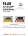
NCV8842PWGEVB
Table 1. ABSOLUTE MAXIMUM RATINGS
Pin Name
Maximum Voltage
Maximum Current
VIN
16 V
2.0 A
VOUT
10 V
2.0 A
SHDNB
7.0 V
1.0 mA
SYNC
7.0 V
1.0 mA
Stresses exceeding Maximum Ratings may damage the board. Maximum Ratings are stress ratings only. Functional operation above the
Recommended Operating Conditions is not implied.
Table 2. NCV8842 SOIC EVALUATION BOARD USER TERMINALS
VIN
Positive DC input voltage, 7 V to 16 V
GND
Common power negative / signal return
VOUT
Regulated DC output voltage
SHDNB
Shutdown−bar signal. Leave open or drive high for normal operation, drive low to force the regulator into
sleep/shutdown mode.
SYNC
Input signal to synchronize to converter oscillator to a higher external frequency source. Leave open if unused.
BR1, BR2, BR3
Bridges (jumpers) for programming the regulated output voltage to one of three levels. Always bridge one pair of
terminals.
Terminals bridged
VOUT
BR1
2.5 V
BR2
3.3 V
BR3
5.0 V
Table 3. ELECTRICAL CHARACTERISTICS
(TA = 25°C, 7.0 V ≤ VIN ≤ 16 V, 0.1 A ≤ IOUT ≤ 1.0 A, unless otherwise specified.)
Characteristic
Test Conditions
Typ
Unit
−
4.0
%
Line Regulation
No Load
0.02
%
Load Regulation
VIN = 7.0 V
0.15
%
−
3.0
%
Load toggle between 0.1 A and 1.0 A
10
μs
−
5.0
ms
−
3.3
V
Sync Frequency
−
190 to 355
kHz
Minimum Sync Threshold Voltage
−
1.0
V
Minimum Shutdown Threshold Voltage
−
0.3
V
Maximum Shutdown Bias Current
−
12
mA
−
170
kHz
ILOAD = 100 mA
ILOAD = 1.0 A
77.5
83
%
%
−
1.0
mA
Output Voltage
Voltage Accuracy
Transient Response
Transient Response Time
Startup Time
Input Voltage
Start Threshold
Sync and Shutdown
General
Switching Frequency
Efficiency
Shutdown Current*
*If a pull−up resistor is employed, the shutdown current is increased drastically (Vin/R).
http://onsemi.com
2