1
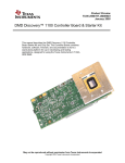
Product Preview TI DN 2506197 z0800003 March 2006 DMD Discovery™ 1100 Controller Board & Starter Kit This manual describes the DMD Discovery 1100 Controller Board Starter Kit and Chip Set. The Controller Board combines hardware, software, firmware, and documentation to form a stand-alone platform for use in developing and testing applications, designed for using the Texas Instruments 0.7 XGA DDR DMD. May not be reproduced without permission from Texas Instruments Incorporated Copyright 2004 Texas Instruments Incorporated Discovery 1100 Controller Board & Starter Kit Product Preview IMPORTANT NOTICE Texas Instruments and its subsidiaries (TI) reserve the right to make changes to their products or to discontinue any product or service without notice, and advise customers to obtain the latest version of relevant information to verify, before placing orders, that information being relied on is current and complete. All products are sold subject to the terms and conditions of sale supplied at the time of order acknowledgment, including those pertaining to warranty, patent infringement, and limitation of liability. In no event shall TI be liable for any special, incidental, consequential or indirect damages however caused, arising in anyway from the sale or use of the TI products. Products purchased from a TI authorized distributor are subject to the distributor’s terms and conditions of sale. TI warrants performance of its semiconductor products to the specifications applicable at the time of sale in accordance with TI’s standard warranty. Testing and other quality control techniques are utilized to the extent TI deems necessary to support this warranty. Specific testing of all parameters of each device is not necessarily performed, except those mandated by government requirements. Customers are responsible for their applications using TI components unless otherwise stated, this documentation and its intellectual content is copyrighted or provided under license and may not be distributed in any form without the express written permission of Texas Instruments Incorporated. Certain applications using semiconductor products may involve potential risks of death, personal injury, or severe property or environmental damage (“critical applications”). TI semiconductor products are not designed, authorized, or warranted to be suitable for use in life-support devices or systems or other critical applications. Inclusion of TI products in such applications is understood to be fully at the customer’s risk. In order to minimize risks associated with the customer’s applications, adequate design and operating safeguards must be provided by the customer to minimize inherent or procedural hazards. TI assumes no liability for applications assistance or customer product design. TI does not warrant or represent that any license, either express or implied, is granted under any patent right, copyright, mask work right, or other intellectual property right of TI covering or relating to any combination, machine, or process in which such semiconductor products or services might be or are used. TI’s publication of information regarding any third party’s products or services does not constitute TI’s approval, warranty or endorsement thereof. Trademarks Microsoft, Windows, Microsoft ActiveX, Windows XP and Windows 2000 are trademarks of Microsoft Corporation. Other trademarks are the property of their respective owners. May not be reproduced without permission from Texas Instruments Incorporated Copyright 2004 Texas Instruments Incorporated i TI DN 2506197 Discovery 1100 Controller Board & Starter Kit Product Preview Notational Conventions This document uses the following conventions. The Discovery 1100 Controller Board is also referred to as Controller Board. Program listings, program examples, and interactive displays are shown as a special typeface similar to a typewriter’s. Some examples use a bold version of the special typeface for emphasis; interactive displays use a bold version of the special typeface to distinguish commands that you enter from items that the system displays (such as prompts, command output, error messages, etc.). Here is a sample program listing: 0011 0012 0013 0014 0005 0005 0005 0006 0001 .field 1, 2 0003 .field 3, 4 0006 .field 6, 3 .even In syntax descriptions, the instruction, command, or directive is in a bold typeface font and parameters are in an italic typeface. Portions of the syntax that are bold should be entered as shown; portions of syntax that are in italics describe the type of information that should be entered. Syntax that is entered on a command line is centered. Syntax that is used in a text file is left justified. Square brackets ([and]) identify an optional parameter. If you use an optional parameter, you specify the information within the brackets. Unless the square brackets are in a bold typeface, do not enter the brackets themselves. Information About Cautions and Warnings This book may contain cautions and warnings. This is a description of a caution statement: A caution statement describes a situation that could potentially damage your software or equipment. This is a description of a warning statement: A warning statement describes a situation that could potentially cause harm to you. The information in a caution or a warning is provided for your protection. Please read each caution and warning carefully. May not be reproduced without permission from Texas Instruments Incorporated Copyright 2004 Texas Instruments Incorporated ii TI DN 2506197 Discovery 1100 Controller Board & Starter Kit Product Preview EVALUATION BOARD/KIT IMPORTANT NOTICE Texas Instruments (TI) provides the enclosed product(s) under the following conditions: This evaluation board/kit being sold by TI is intended for use for ENGINEERING DEVELOPMENT OR EVALUATION PURPOSES ONLY and is not considered by TI to be fit for general consumer use. Persons handling the product(s) must have electronics training and observe good engineering practice standards. As such, the goods being provided may not be complete in terms of required design-, marketing-, and/or manufacturing-related protective considerations, including product safety and environmental measures typically found in end products that incorporate such semiconductor components or circuit boards. This evaluation board/kit does not fall within the scope of the European Union directives regarding electromagnetic compatibility, restricted substances (RoHS), or recycling (WEEE), and therefore may not meet the technical requirements of these directives or other related directives. Should this evaluation board/kit not meet the specifications indicated in the User’s Guide, the board/kit may be returned within 30 days from the date of delivery for a full refund. THE FOREGOING WARRANTY IS THE EXCLUSIVE WARRANTY MADE BY SELLER TO BUYER AND IS IN LIEU OF ALL OTHER WARRANTIES, EXPRESSED, IMPLIED, OR STATUTORY, INCLUDING ANY WARRANTY OF MERCHANTABILITY OR FITNESS FOR ANY PARTICULAR PURPOSE. The user assumes all responsibility and liability for proper and safe handling of the goods. Further, the user indemnifies TI from all claims arising from the handling or use of the goods. Please be aware that the products received may not be regulatory compliant or agency certified (FCC, UL, CE, RoHS, WEEE etc.). Due to the open construction of the product, it is the user’s responsibility to take any and all appropriate precautions with regard to electrostatic discharge. EXCEPT TO THE EXTENT OF THE INDEMNITY SET FORTH ABOVE, NEITHER PARTY SHALL BE LIABLE TO THE OTHER FOR ANY INDIRECT, SPECIAL, INCIDENTAL, OR CONSEQUENTIAL DAMAGES. TI currently deals with a variety of customers for products, and therefore our arrangement with the user is not exclusive. TI assumes no liability for applications assistance, customer product design, software performance, or infringement of patents or services described herein. Please read the User’s Guide and, specifically, the Warnings and Restrictions notice in the User’s Guide prior to handling the product. This notice contains important safety information about temperatures and voltages. For further safety concerns, please contact the TI application engineer. No license is granted under any patent right or other intellectual property right of TI covering or relating to any machine, process, or combination in which such TI products or services might be or are used. Mailing Address: Texas Instruments Post Office Box 655303 Dallas, Texas 75265 FCC Warning This evaluation board/kit is intended for use in an engineering test environment only. It generates, uses, and can radiate radio frequency energy and has not been tested for compliance with the limits of computing devices pursuant to part 15 of FCC rules, which are designed to provide reasonable protection against radio frequency interference. Operation of this equipment in other environments may cause interference with radio communications, in which case the user at their own expense will be required to take whatever measures may be required to correct this interference. May not be reproduced without permission from Texas Instruments Incorporated Copyright 2004 Texas Instruments Incorporated iii TI DN 2506197 Discovery 1100 Controller Board & Starter Kit Product Preview Table of Contents 1 Introduction........................................................................................................................................ 1 1.1 Overview.................................................................................................................................... 1 1.2 Features..................................................................................................................................... 1 1.3 Key Components ....................................................................................................................... 3 1.3.1 DMD Optical Modulator ................................................................................................ 3 1.3.2 DAD1000 Reset Driver ................................................................................................. 3 1.3.3 High Speed Controller (HSC) ....................................................................................... 4 1.3.4 DAD1000 Reset Controller (DRC)................................................................................ 4 1.3.5 USB Interface Controller (USBIFC).............................................................................. 4 1.3.6 USB Controller.............................................................................................................. 4 2 Getting Started................................................................................................................................... 5 2.1 Host PC Requirements.............................................................................................................. 5 2.2 How to Connect to the Controller Board.................................................................................... 5 2.3 USB 2.0 Port Connection .......................................................................................................... 6 2.4 High-Speed Port Connection..................................................................................................... 6 2.5 Power Requirements ................................................................................................................. 6 2.6 Protection Features ................................................................................................................... 6 2.7 Modes of Operation ................................................................................................................... 6 3 Controller Configuration................................................................................................................... 7 3.1 High-Speed Port Clock Frequency Selection ............................................................................ 7 3.2 High-Speed Clock source selection........................................................................................... 7 4 External Connections ..................................................................................................................... 10 4.1 High-Speed Port Interface Connection.................................................................................... 10 4.2 USB Port Connection .............................................................................................................. 11 5 Port Specification Overview........................................................................................................... 12 5.1 High-Speed Port ...................................................................................................................... 12 5.1.1 Electrical Interface ...................................................................................................... 13 5.1.2 Connector ................................................................................................................... 21 5.1.3 System Clock.............................................................................................................. 21 5.2 USB Port.................................................................................................................................. 21 5.2.1 Electrical Interface ...................................................................................................... 21 5.2.2 Commands ................................................................................................................. 21 6 Discovery Controller Printed Circuit Board Configuration......................................................... 23 7 User Connectors and I/O ................................................................................................................ 25 7.1 J1 Connector Pin Outs ............................................................................................................ 26 7.2 J2 Connector Pin Outs ............................................................................................................ 26 7.3 J6 Connector Pin Outs ............................................................................................................ 26 7.4 J7 Connector Pin Outs ............................................................................................................ 26 7.5 J3 Connector Pin Outs ............................................................................................................ 27 7.6 J4 Connector Pin Outs ............................................................................................................ 28 8 Diagnostics ...................................................................................................................................... 29 8.1 Power and Status LEDs .......................................................................................................... 29 9 Critical Timing Characteristics ...................................................................................................... 30 9.1 TIMING CHARACTERISTICS ................................................................................................. 31 May not be reproduced without permission from Texas Instruments Incorporated Copyright 2004 Texas Instruments Incorporated iv TI DN 2506197 Discovery 1100 Controller Board & Starter Kit Product Preview List of Illustrations Figure 1 Discovery Controller Board, Top View.................................................................................................................... 2 Figure 2 Discovery Controller Board, Bottom View............................................................................................................... 2 Figure 3 Discovery Controller Board Block Diagram ............................................................................................................ 3 Figure 4 Discovery Controller Board Setup .......................................................................................................................... 5 Figure 5 Clock Frequency Selection ..................................................................................................................................... 8 Figure 6 Clock Source Selection with resistors..................................................................................................................... 8 Figure 7 Clock Source Selection with jumpers ..................................................................................................................... 9 Figure 8 Controller Board to High-Speed Daughter Board ................................................................................................. 10 Figure 9 Discovery Controller Board Connected to High-Speed Daughter Board.............................................................. 11 Figure 10 USB Cable Connection ......................................................................................................................................... 11 Figure 11 DMD Data Format................................................................................................................................................ 14 Figure 12 Typical Write Sequence ....................................................................................................................................... 17 Figure 13 Typical Phased Reset Sequence......................................................................................................................... 18 Figure 14 Typical Load and Reset Sequence on a single block with Mirror settling ........................................................... 19 Figure 15 Discovery Controller Board Silkscreen, Top View ............................................................................................... 23 Figure 16 Discovery Controller Board Silkscreen, Bottom View.......................................................................................... 24 Figure 17 DMD Bit Addressing............................................................................................................................................. 24 Figure 18 Controller Board Connector Locations................................................................................................................. 25 Figure 19 Controller Board Indicators .................................................................................................................................. 29 Figure 20 DATACLK Timing................................................................................................................................................. 31 Figure 21 DATACLK to DATAVALID Requirements............................................................................................................ 31 Figure 22 Line Control Bits setup and hold requirements.................................................................................................... 31 Figure 23 Reset Timing........................................................................................................................................................ 31 Figure 24 Global Reset Timing ............................................................................................................................................ 32 Figure 25 DMD Thermal test points ..................................................................................................................................... 33 List of Tables Table 1 Clock frequency selection resistors ......................................................................................................................... 7 Table 2 Clock source selection ............................................................................................................................................. 7 Table 3 High-Speed Port I/O Pins (Pin #s not available for preview.) ................................................................................ 13 Table 4 Address Mode Select Bits (not available for preview) ........................................................................................... 16 Table 5 Data Write Bit Sequence (not available for preview) ............................................................................................. 16 Table 6 Global Clear Memory- Global Clear Memory (not available for preview) .............................................................. 18 Table 7 Reset Groups (Select bits not available for preview.)............................................................................................ 20 Table 8 Connector J1.......................................................................................................................................................... 26 Table 9 Connector J2.......................................................................................................................................................... 26 Table 10 Connector J6......................................................................................................................................................... 26 Table 11 Connector J7......................................................................................................................................................... 26 Table 12 Connector J3 (not available for preview) .............................................................................................................. 27 Table 13 Connector J4 (not available for preview) .............................................................................................................. 28 Table 14 Diagnostic Indicators............................................................................................................................................. 29 Table 15 Critical Timing Characteristics (not available for preview) .................................................................................... 30 Table 16 Absolute Maximum Ratings .................................................................................................................................. 33 Table 17 Recommended Operating Condition..................................................................................................................... 34 May not be reproduced without permission from Texas Instruments Incorporated Copyright 2004 Texas Instruments Incorporated v TI DN 2506197 Discovery 1100 Controller Board & Starter Kit Product Preview Chapter 1 – Introduction 1 Introduction This section gives a general definition of the Discovery 1100 Product Family, consisting of Starter Kit and Discovery 1100 Chip Set. The Starter Kit consists of the following components: Discovery 1100 Controller Board An ActiveX control (Win XP/2000) A GUI (Win XP/2000) Documentation CD, User manual and documentation for both the module and the core component set (HSC, DRC, and USBIFC Controllers) USB 2.0 Cable Power supply (with European version options) The Discovery 1100 Chip Set consists of the Texas Instruments 0.7 XGA DDR DMD, DAD1000 Power and Reset Driver, and the Discovery 1100 Digital Controller Chipset (HSC, DRC and USBIFC). 1.1 Overview The following is a high level description of the different components and benefits that comprise the Controller Board. The system provides: A simplified standard development system for general application of the DMD. This system is a cost effective, small footprint product that allows users to quickly apply DMD devices for most applications. USB 2.0 and 64-bit High-Speed interfaces. interface with the DMD via a controller. A thin GUI layer that interfaces using Microsoft ActiveX controls and is used to control the hardware via the USB interface. Both interfaces accept data and command signals that 1.2 Features The features of the Controller Board include the following: • 0.7 XGA DDR DMD in a socket for easy replacement. • DAD1000 Power and Reset Driver. • Discovery 1100 Digital Controller Chipset (HSC, DRC, USBIFC) • For custom slower speed designs the HSC may be excluded • For custom High-Speed designs the USB Controller and USBIFC may be excluded • USB 2.0 port (Can display images in excess of 100 fps, depending on system). • 64-bit High-Speed data port (120MHz maximum Single Data Rate interface). • External Strobe port for precise DMD Reset pulse timing. • Control of Controller Board via USB or High-Speed interface. • Individual DMD reset blocks may be loaded and operated with some restrictions. May not be reproduced without permission from Texas Instruments Incorporated Copyright 2004 Texas Instruments Incorporated -1TI DN 2506197 Discovery 1100 Controller Board & Starter Kit Product Preview • Logic protection prevents damage to the DMD due to improper operation of Discovery board. The logic protection also places the DMD mirrors to a safe non-deflected position during inactivity. Figure 1 and Figure 2 show the locations of some of the major components. USB Connector USB Controller DRC HSC High-Speed Ports USBIF DAD1000 Figure 1 Discovery Controller Board, Top View 0.7 XGA DDR DMD Figure 2 Discovery Controller Board, Bottom View May not be reproduced without permission from Texas Instruments Incorporated Copyright 2004 Texas Instruments Incorporated -2TI DN 2506197 Discovery 1100 Controller Board & Starter Kit Product Preview 1.3 Key Components Key components are shown in the block diagram below and described in the following paragraphs. TEXAS INSTRUMENTS RESET(0:15) TEXAS INSTRUMENTS VCC2 DAD1000 RESET DRIVER Cypress FX2 USB 0.7 XGA DMD DMD_CMD SCP 1024 x 768 PIXELS Discovery 1100 HSC Discovery 1100 DRC Discovery 1100 USBIFC DCLK DMD_CMD BUFFERS USB EN USB_DMD_D(0:63) USB USER INTERFACE Reset and Block Control Clock Input/Data Valid DATA(0:63) HIGH-SPEED USER INTERFACE Figure 3 Discovery Controller Board Block Diagram 1.3.1 DMD Optical Modulator The Controller Board uses the Texas Instruments DMD 0.7 XGA DDR (Double Data Rate) device. The DMD 0.7XGA 12° DDR is a spatial light modulator that consists of a 1024 (H) x 768 (V) array of aluminum micromechanical mirrors on a 13.68-micrometer (um) pitch. Each mirror is individually deflected at an angle about a hinged diagonal axis. Deflection polarity (positive or negative) of the mirrors is controlled by changing the address voltage of underlying CMOS addressing circuitry and mirror reset signals. Data is clocked in on the leading and falling edge of the internal DMD data clock. The 1024 x 768 mirrors are driven in a Block Reset fashion. This block reset provides the functionality of controlling a single or multiple blocks on the DMD that in turn allows for either a global or phased reset. Effectively, the DMD 0.7XGA 12° DDR is an electrical input, optical output memory device. A Pond Of Mirrors (POM) border area consisting of six mirrors and an asymmetrical Dark Metal border, on all four sides, surrounds the array. The device is mounted using a pressure socket, and is equipped with a mounting surface for optical interfacing. For more information on the DMD 0.7XGA DDR 12, refer to the DMD .7 XGA DDR Discovery User Data Sheet, TI DN 2503884. 1.3.2 DAD1000 Reset Driver The TI DAD1000 reset driver provides the high voltage power and reset driver functions for the DMD. The DRC controls the DAD1000. For more information on the DAD1000 reset driver, refer to the DAD1000 Power and Reset Driver Discovery User Data Sheet, TI DN 2503885. May not be reproduced without permission from Texas Instruments Incorporated Copyright 2004 Texas Instruments Incorporated -3TI DN 2506197 Discovery 1100 Controller Board & Starter Kit Product Preview 1.3.3 High Speed Controller (HSC) The HSC provides the control needed to drive at high-speed the Discovery’s DMD. The HSC device also provides conversion from SDR to DDR clock generation and selection between High-Speed port and USB control of the DMD. This device is not required for custom USB only designs. For more information on the HSC, refer to the Discovery 1100 HSC Customer Data Sheet, TI DN 2506019. 1.3.4 DAD1000 Reset Controller (DRC) The DRC provides the interface to the DAD Reset Driver that provides reset functions for the DMD. The controller times resets and allows for overlapping block resets. At any one time, three block resets can be controlled at one time. This device is also responsible for DMD and DAD initialization. For more information on the DRC, refer to the Discovery 1100 DRC Customer Data Sheet, TI DN 2506020. 1.3.5 USB Interface Controller (USBIFC) The USBIFC provides all required interface from the USB Controller to the DMD. The USBIFC device buffers data and provides the required clocking to the DMD. This device is not required for custom High-Speed only designs. For more information on the USBIFC, refer to the Discovery 1100 USBIFC Customer Data Sheet, TI DN 2506018. 1.3.6 USB Controller The USB Controller is a Cypress CY7C68013 FX2 single chip USB 2.0 controller operating at 480 Mbits. The device has an integrated CPU based on the 8051. When used with the USBIFC, this controller provides all the control of the DMD through commands and data sent over the USB link. This device is not required for custom High-Speed only designs. May not be reproduced without permission from Texas Instruments Incorporated Copyright 2004 Texas Instruments Incorporated -4TI DN 2506197 Discovery 1100 Controller Board & Starter Kit Product Preview Chapter 2 – Getting Started 2 Getting Started The Controller Board requires a switching mode power supply rated at +5V @ 2.0A. 2.1 Host PC Requirements The following equipment is required for use with Controller Board. One personal computer host with the following: 233 MHz Pentium processor or equivalent 128Mbytes RAM USB 2.0 port Hard disk drive with additional 30 Megabytes of available disk space SVGA (800 x 600) display minimum (1024x768 recommended) Local CD-ROM drive Windows 2000 or XP 2.2 How to Connect to the Controller Board Figure 1 shows all the basic connection points to the Controller Board. connections made using the High-Speed port and USB connectors. Chapter 3 illustrates the external Discovery Controller Host PC USB Connection External Power Source External Reset DMD (Back Side of Board) High Speed Port Customer Data Source Printed wiring Board Figure 4 Discovery Controller Board Setup May not be reproduced without permission from Texas Instruments Incorporated Copyright 2004 Texas Instruments Incorporated -5TI DN 2506197 Discovery 1100 Controller Board & Starter Kit Product Preview 2.3 USB 2.0 Port Connection USB 2.0 port is a standard way of connecting the Discovery board to a host system. It provides a reliable low cost connection to a host computer at a rate in excess of 100 frames per second. 2.4 High-Speed Port Connection The Controller Board utilizes two connectors on the opposite side of the board to provide a short equi-distant electrical path for data signals from the High-Speed Port connectors to the DMD High-Speed FET bus switches. Placement of devices that handle high-speed signals to the connectors should be taken into consideration in the design of a High-Speed Port daughter board. It is suggested that these devices be placed between the connectors in a manner similar to the Controller Board. 2.5 Power Requirements A 4-pin low profile connector (J7) is provided to bring power in from a remote power supply furnishing +12Vdc @ 0.5A and +5VDC @ 1.5A. This 4-pin connector accepts a standard computer ATX type power supply. An alternate 5VDC only power connector (J8) through a 2mm DC power connector is available to provide +5VDC @ 2.0A (recommended for new designs). 2.6 Protection Features The Discovery Controller Board provides protection logic sequencing control for the DMD as follows: 1) In the event of power failure, the DMD will be issued a FLOAT command that will place all mirrors in a nondeflected position. 2) The DMD is also protected against MPU inactivity by application of an automatic RESET command. MPU inactivity is defined as no resets being issued within a 10 second period. In this condition, the following sequence will occur: A “watchdog” timer connected to the Digital Controller will begin to count down. If resets do not start again within 10 seconds, the watchdog timer will send a reset command. This feature can be disabled by removal of R88. 2.7 Modes of Operation The Controller Board is designed to operate in either USB or High-Speed mode, but not both. On power up, the board will initialize automatically in High-Speed Mode. If a USB cable is plugged into the Discovery’s USB port, then the controller will switch to USB mode. May not be reproduced without permission from Texas Instruments Incorporated Copyright 2004 Texas Instruments Incorporated -6TI DN 2506197 Discovery 1100 Controller Board & Starter Kit Product Preview Chapter 3 – Controller Configuration 3 Controller Configuration The DMD Discovery 1100 provides two timing mechanisms. These two mechanisms are an onboard internal clock and an external clock. The Discovery 1100 operates using a 120 MHz on-board clock to provide internal timing for the HSC. This clock connects to the HSC and outputs to the high-speed port at J4 pin 88. The frequency of this clock is defaulted to 120 MHz but may be set to be one of four rates. The Discovery 1100 board also allows an application to provide an external clock through the High-Speed Port connector pin 88 on J4. When the Discovery 1100 is set for external clock, DATACLK becomes the input clock on the Discovery 1100 and is connected to the HSC. For more details on clock frequency and source selection, see the Discovery 1100 HSC Customer Data Sheet, TI DN 2506019 and the Discovery 1100 Schematics, TI DN 2506026 3.1 High-Speed Port Clock Frequency Selection The default frequency for the high-speed port clock is 120MHz. This frequency may be changed to 15, 30 or 60 MHz by using resistors R45, R46, R47, and R48 to control the clock frequency. To change from the default frequency install the resistors listed in Table 1. All resistors are 1000 ohms. See Figure 5 for the location of these resistors. Table 1 Clock frequency selection resistors Install Frequency R47 R48 15 MHZ R45 R48 30MHZ R46 R47 60MHZ R45 R46 120MHZ 3.2 High-Speed Clock source selection The source of the clock can be selected as either internal (supplied by Discovery 1100) or external (supplied through a High-Speed interface). All boards are shipped configured for internal clock and need to be reconfigured to use with an external clock. To change the configuration of Discovery 1100 board to accept an external clock install the resistors or jumpers listed in Table 2. All resistors are 22 ohms. See Figure 6 and Figure 7 for the location of these resistors and jumpers. Table 2 Clock source selection Function Install External Clock R95 Internal Clock R94 R97 May not be reproduced without permission from Texas Instruments Incorporated Copyright 2004 Texas Instruments Incorporated -7TI DN 2506197 Discovery 1100 Controller Board & Starter Kit Product Preview R48, R46, R45, R47 Figure 5 Clock Frequency Selection R97, R95, R94 Figure 6 Clock Source Selection with resistors May not be reproduced without permission from Texas Instruments Incorporated Copyright 2004 Texas Instruments Incorporated -8TI DN 2506197 Discovery 1100 Controller Board & Starter Kit Product Preview R97, R95, R94 Figure 7 Clock Source Selection with jumpers May not be reproduced without permission from Texas Instruments Incorporated Copyright 2004 Texas Instruments Incorporated -9TI DN 2506197 Discovery 1100 Controller Board & Starter Kit Product Preview Chapter 4 External Connections 4 External Connections For applications at or below a 100 Hz binary frame rate, the USB Mode allows control of the Controller Board hardware by sending commands and data via the USB interface. For very high-speed applications (frame rate > 100 frames per sec), the High-Speed Mode allows data to be routed via a High-Speed interface. In figures 7 and 8, a High-Speed daughter card is shown as an example of how a High-Speed LVTTL interface may be designed. 4.1 High-Speed Port Interface Connection Images and commands are sent down via the High-Speed Port while the USB port is inactive. Chapter 5 provides more detailed information on the High-Speed Port functionality. Figure 8 illustrates how a High-Speed interface board may be connected to the Controller Board. Figure 9 shows how the two boards look after being connected. Controller Board High-Speed Port Connectors High-Speed Daughter Board Connectors Figure 8 Controller Board to High-Speed Daughter Board May not be reproduced without permission from Texas Instruments Incorporated Copyright 2004 Texas Instruments Incorporated - 10 TI DN 2506197 Discovery 1100 Controller Board & Starter Kit Product Preview Figure 9 Discovery Controller Board Connected to High-Speed Daughter Board 4.2 USB Port Connection The USB Port is used for serial access control and data signals along with graphic files. Images, commands, and responses are sent down to and retrieved from the device via USB. Chapter 5 provides more detailed information on the USB Port functionality. Figure 10 USB Cable Connection May not be reproduced without permission from Texas Instruments Incorporated Copyright 2004 Texas Instruments Incorporated - 11 TI DN 2506197 Discovery 1100 Controller Board & Starter Kit Product Preview Chapter 5 – Port Specifications 5 Port Specification Overview The Discovery Controller Board is equipped with two data ports. The USB 2.0 port is a convenient and practical way of connecting to the Discovery boards for applications requiring frame rates of 100 Hz or less. The second data port is the High-Speed port. This High-Speed port provides the control needed for the High-Speed controller signals by connecting the Discovery High-Speed port to an application interface board. The High-Speed port, when connected to a host system will allow the flexibility of variable frame rate for custom applications. See section 9 for specific timing requirements for the Discovery 1100 and the Discovery 1100 Customer Datasheets for detailed chip information. The following paragraphs describe the different ports on the Controller Board. 5.1 High-Speed Port The High-Speed port is used in situations where the user requires high-speed access to hardware. In this situation, the application must take a more direct control of the logic. Four basic operations are performed using the HighSpeed port. The first operation is control of the reset waveform generator. The generator is used to move the mirrors to a new state, as defined by the contents of the memory cells below the mirrors. The user can choose to reset a single block of mirrors or the entire array. The second operation is the write enable line used to enable the write capabilities to the DMD. The write enable allows an application to write data into memory one line at a time. To write a single line of data, the DMD requires 16 data clocks per cycle, for a total of 1024 bits. Memory operations must be synchronous to the clock, and line control bits must meet prescribed setup and hold times. The third operation makes it possible to adjust the memory row address counter pointer. The memory pointer operation is implemented as a 768-bit shift register but it is not possible to initialize it to a specific location. The application can start at the top or bottom and advances the pointer either up or down, one line at a time, each requiring 16 data clock cycles. By disabling the write enable line; the user can manipulate the line pointer without writing data to the memories. The application must provide for the latency between the setting of the line control bits and the action within the DMD. The final operation available to the user through the High-Speed port is a rapid clear operation. This operation allows the application to quickly clear the entire memory array by clearing 16 lines for each line written to the DMD. The application must send the correct sequence to complete the cycle properly. May not be reproduced without permission from Texas Instruments Incorporated Copyright 2004 Texas Instruments Incorporated - 12 TI DN 2506197 Discovery 1100 Controller Board & Starter Kit Product Preview 5.1.1 Electrical Interface The High-Speed interface is implemented in single-ended LVTTL logic. Table 3 provides signal names and function descriptions for the High-Speed Port I/O pins. The sections following Table 3 describe how these signals are used. The terms “asserted” and “de-asserted” refer to the signal’s “active” and “inactive” states. Line control bits are the signals required to control how data is written to DMD memory. A_MODE[1:0], WRITE_EN AND GLBCLRMEM. These include Table 3 High-Speed Port I/O Pins (Pin #s not available for preview.) Signal Name Pin Number Function I/O DATA [0:63] Data input Input DATACLK Reference Clock Output or Input RDYTOACPT Interface Ready Output INIT_DMD Discovery in Initialization Output DATAVALID Used to start and stop DMD data write sequence Input LINE_SYNC A_MODE1 A_MODE0 WRITE_EN GLBCLRMEM RESET_REQ Line cycle tracking Address Counter Control Address Counter Control Write to Memory Global Clear Memory Bit Change Mirror State Output Notes Buffered DMD Data Select from 120MHz, 60MHz, 30MHz or 10MHz Ready to accept data from interface. Indicates when Discovery is in initialization after power up. Synchronous to DATACLK. Triggers data and command load sequences into memory. Should not be used for timing. Input DMD row address counter control Input DMD row address counter control Input Input Flag sensed by hardware to allow write to DMD memory. Set DMD up for rapid Global Clear operation Input Request Reset Sequence to begin BLK_ADDR3 Input MSB of Reset command mode BLK_ADDR2 Input Bit 2 of Reset command mode BLK_ADDR1 Input Bit 1 of Reset command mode BLK_ADDR0 Input LSB of Reset command mode Reset all mirror blocks GLOBAL_RST Select Global reset Input RESET_ACTIVE Status of Reset Output TRC Data Inversion Input Inverts data into DMD Input Used with BLK_ADR Input Used with BLK_ADR Input Request to place mirrors in unlatched position DAD_MODE0 DAD_MODE1 FLOAT Reset Block Selection Reset Block Selection Float Request Reset command being processed May not be reproduced without permission from Texas Instruments Incorporated Copyright 2004 Texas Instruments Incorporated - 13 TI DN 2506197 Discovery 1100 Controller Board & Starter Kit Product Preview 5.1.1.1 Data Interface (DATA [0:63]) The data interface to the DMD is via 64 High-Speed lines. Data is latched in on the falling edges of the DATACLK. Sixteen DATACLK cycles are required to load one line of data. The user must load a minimum of one line per transaction or 16 DATACLK cycles. The entire array may be loaded without stopping. The presentation of the data on the data lines must correspond with the DATAVALID signal. Figure 11 shows an example of data for a single line. Data is written to the DMD 64 bits at a time. An entire line must be written for data to be latched into memory and it requires 16 clock cycles to write a single line of 1024 bits. DATA[0:63] 16th Clock 15th Clock : 2nd Clock 1st Clock 0 1 : 14 15 D0 992 993 : 1006 1007 D62 16 17 : 30 31 D1 1008 1009 : 1022 1023 D63 Row Data (0-15) (16-31) (992-1007) (1008-1023) Mirror Block Drivers (0:15) TRC CMD0/1 DCLK Data Transfer Control Row Address Shift Register (0:767) 64 X 16-bit Shift Registers 1024 Parallel Latches & Data Column Drivers Mirror Block Control CMD2/3 MBRST(0:15) VCC2 Figure 11 DMD Data Format May not be reproduced without permission from Texas Instruments Incorporated Copyright 2004 Texas Instruments Incorporated - 14 TI DN 2506197 Discovery 1100 Controller Board & Starter Kit Product Preview 5.1.1.2 Clock Reference (DATACLK) In the internal clock mode, the Controller Board provides the clock, and data must be transmitted synchronously to the clock. The clock operates continuously at one of four frequency options (120MHz, 60MHz, 30MHz or 15MHz). See Table 1 for the resistor configuration to select the desired frequency. DATACLK can also be provided through J4 if the Discovery is configured for external clock. All timing and data relationships must still be met. See Table 2 for resistor or jumper configuration to select internal or external clock. 5.1.1.3 Ready to Accept Data (RDYTOACPT) When the hardware is ready to accept data via the High-Speed port, it will assert this signal. Normally, this signal is low on power-up and asserted when the Controller Board has initialized itself. This signal is terminated with a 1K ohm pull down resistor. 5.1.1.4 Discovery in Initialization (INIT_DMD) This signal indicates that the Discovery is in an initialization state after power is applied. During this initialization period, the DRC is initializing the DAD1000 by setting all internal registers to their correct states, and then initiating a DMD mirror reset. This signal also initializes the HSC and USBIFC controllers. When this signal goes high, the DRC has completed initialization. 5.1.1.5 Data and Command Valid Signal (DATAVALID) If RDYTOACPT is asserted, the user is free to synchronously send data to the DMD using timing provided by the HSC. All operations are completed on a line-by-line cycle. The cycle period is exactly 16 HS_CLK clocks long and begins with DATAVALID as shown in Figure 12. A minimum of one line cycle or 16 clocks of data must be sent at a time. If DATAVALID is removed, the HSC will stop loading data and stop incrementing DMD row address counters until DATAVALID goes active again. The line control bits to the HSC should be asserted and de-asserted synchronously with DATAVALID and sent 2 lines ahead of the actual DATA. DATAVALID is active LOW. This signal is terminated with a 1K ohm pull up resistor. 5.1.1.6 Line Sync (LINE_SYNC) This is a Discovery 1000 legacy signal. The purpose of Line Sync was to provide a method to keep track of when each line was written. The signal would indicate when a write line sequence had completed at the end of the each line. It is not recommended to be used for new designs. 5.1.1.7 Address Mode Select Bits (A_MODE [1:0]) A_MODE [1:0] are used to control the operation of the DMD row address counter that is used to determine the line to which DMD data is written. The counter may be cleared, set to 767, incremented, or decremented. The user must comprehend the latency, as shown in Figure 12, to coordinate the action of the control bits. Refer to Table 4 for a description of the bit patterns. Note that the pointer will increment, decrement, set to the top or set to the bottom each time a memory cycle is performed. There is no way to hold, preset or jump the address. If a memory cycle is not active, the pointer will remain at the last position. The DMD 0.7XGA 12° DDR does not have an automatic wrap-around row address counter (i.e. row 766,767,0,1, …). After row 767, the row address counter must be cleared to zero, to start the row address counter at Row 0. These signals are terminated with 1K ohm pull down resistors. May not be reproduced without permission from Texas Instruments Incorporated Copyright 2004 Texas Instruments Incorporated - 15 TI DN 2506197 Discovery 1100 Controller Board & Starter Kit Product Preview Table 4 Address Mode Select Bits (not available for preview) A_MODE1 5.1.1.8 A_MODE0 Function Write Enable (WRITE_EN) De-asserting the write enable flag enables the application to manipulate the address counter, without performing a write to the row being addressed prior to the operation. This bit must be set low during a global clear operation. WRITE_EN is active HIGH. Table 5 shows a 4-line write sequence. This signal is terminated with a 1K ohm pull down resistor. A_MODE0 A_MODE1 WRITE_EN Command GLBCLRMEM Table 5 Data Write Bit Sequence (not available for preview) DATA [0:63] Comments A line control bit example illustrating the process of writing data into the DMD memory is provided in Table 5 and Figure 12. Line Cycle 1 of Table 5 and Figure 12 shows the initial condition of writing data. Note that the line control bits for Line Cycle 2 and are latched in at the end of cycle 1 as shown in Table 5. May not be reproduced without permission from Texas Instruments Incorporated Copyright 2004 Texas Instruments Incorporated - 16 TI DN 2506197 Discovery 1100 Controller Board & Starter Kit Product Preview CYCLE 1 X 1 2 3 4 5 6 7 8 9 CYCLE 2 10 11 12 13 14 15 16 1 2 3 4 5 6 7 8 9 10 11 12 13 14 15 16 PPORT_DCLK LINE CTRL BITS CTL1 CTL0 DATA [0:63] X X X X X X X X X X X X X X X X X X X X X X X NO DATA WRITTEN/CTL0 WILL SET LINE COUNTER TO 0 OR 767 DATA_VALID 2 3 4 5 6 7 8 9 X X X X X X X X CYCLE 4 CYCLE 3 1 X NO DATA WRITTEN/CTL1 WILL SET LINE COUNTER TO INCREMENT OR DECREMENT 10 11 12 13 14 15 16 1 2 3 4 5 6 7 8 9 10 11 12 13 14 15 16 X PPORT_DCLK LINE CTRL BITS CTL2 DATA [0:63] 15 14 13 12 11 10 9 8 7 6 5 4 3 2 1 0 CTL3 15 14 13 12 11 10 DATA FOR LINE 0 OR 767/CTRL2 STAYS THE SAME 9 8 7 6 5 4 3 2 1 0 DATA FOR LINE 1 OR 766/CTRL3 STAYS THE SAME DATA_VALID INACTIVE X CYCLE 5 1 2 3 4 5 6 7 8 9 CYCLE 6 10 11 12 13 14 15 16 1 2 3 4 5 6 7 8 9 10 11 12 13 14 15 16 X PPORT_DCLK LINE CTRL BITS DATA [0:63] CTL5 CTL4 15 14 13 12 11 10 9 8 7 6 5 4 3 2 DATA FOR LINE 2 OR 765/CTRL4 STAYS THE SAME 1 0 15 14 13 12 11 10 9 8 7 6 5 4 3 2 1 0 DATA FOR LINE 3 OR 764/CTRL5 STAYS THE SAME DATA_VALID Figure 12 Typical Write Sequence 5.1.1.9 Clear memory flag (GLBCLRMEM) The DMD will be placed in the global clear mode when GLBCLEARMEM is set high, and are clocked into the DMD. Normally, it requires 768 line loads to write to every position in the DMD. When this bit is set, it is possible to clear 16 lines at a time, thereby completing the clear operation in 1/16 the time required loading data. Separate counters are used for resetting the DMD under these conditions. This function cannot be used to load data, position the address counter, or set the device to all ones. This bit must be set at the proper value when DATAVALID transitions, and must remain asserted on subsequent lines on 16 clock cycle boundaries. See Table 6 below. This signal is terminated with a 1K ohm pull down resistor. May not be reproduced without permission from Texas Instruments Incorporated Copyright 2004 Texas Instruments Incorporated - 17 TI DN 2506197 Discovery 1100 Controller Board & Starter Kit Product Preview A_MODE0 A_MODE1 WRITE_EN Command GLBCLRMEM Table 6 Global Clear Memory- Global Clear Memory (not available for preview) DATA [0:63] Comments 5.1.1.10 Reset Request (RESET_REQ) and Reset Active (RESET_ACTIVE) The RESET_REQ starts the reset sequence and the RESET_ACTIVE indicates when the reset logic is available to start the next reset. Refer to Figure 13 for a typical reset sequence. It should be noted that no other resets should be initiated while the HS_RESET_ACTIVE signal is active. While a reset function is active (HIGH), this signal indicates that the reset is in process. This signal goes active (high) about 100ns after HS_RESET_REQ goes active (high) and will stay high about 6.2us. While HS_RESET_REQ is high, and for 4-12us after, the data for the block(s) being reset should not be changed to allow for the settling required for the mirrors to become stable. The ability to load new data into other blocks that have not been recently reset is not affected. Figure 14 shows a single block load, reset, and reload sequence with the light gray areas indicating mirror-settling time. The minimum mirror settle time is determined by what DMD mirror design is used. Although a minimum of 12us was required for older, XB DMDs, the mirror settle time for FTP DMDs is 4us. Please see TI DN 2503884 for FTTP and XB DMD part number information. DMD_DATA LOAD DATA BLK X LOAD DATA BLK X+1 LOAD DATA BLK X+2 LOAD DATA BLK X+3 LOAD DATA BLK X+4 HS_RESET_REQ HS_RESET_ACTIVE Figure 13 Typical Phased Reset Sequence May not be reproduced without permission from Texas Instruments Incorporated Copyright 2004 Texas Instruments Incorporated - 18 TI DN 2506197 Discovery 1100 Controller Board & Starter Kit Product Preview DMD_DATA LOAD DATA BLK X 4-12us Mirror Settling Time LOAD DATA BLK X HS_RESET_REQ HS_RESET_ACTIVE Figure 14 Typical Load and Reset Sequence on a single block with Mirror settling 5.1.1.11 GLOBAL RESET (GLOBAL_RST) Global Reset is a function that allows for all 16 blocks of the DMD to be reset at once when the GLOBAL_RST signal is set to an active high. In the example of the last line of Table 7, Global Reset causes the DAD_MODE [0:1] to both be one. For this case, there is no need to set up a block and mode bits. The addition of DAD_MODE bits to the Discovery 1100 allows for flexibility beyond the Discovery 1000 design. The DAD_MODE allows for individual groups of blocks to be phased reset. To reset individual groups of blocks the Global Reset signal must be set to LOW. This signal is terminated with a 1K ohm pull down resistor. 5.1.1.12 Toggle Rate Control (TRC) To reduce the data line transition frequency, a TRC signal is provided to the input port of the data. Setting TRC to logic 1 on the input inverts the data being clocked into the device. Setting TRC to logic 0 on the TRC input specifies no data inversion. This signal is terminated with a 1K ohm pull down resistor. 5.1.1.13 FLOAT FLOAT places the DMD mirrors in an unlatched state. This “float” or non-deflected position does not have a bias applied to it. When a FLOAT is issued (FLOAT when set high), the DMD releases the tension under each mirror so that all mirrors are in a relative flat position. The FLOAT does not set the mirrors to a fix flat state but only releases the tension so that each mirror is randomly floating. It is best to issue a FLOAT and not leave a static image on the DMD for extended periods of time. The command executes automatically on power up or when power fails. This signal is terminated with a 1K ohm pull down resistor. May not be reproduced without permission from Texas Instruments Incorporated Copyright 2004 Texas Instruments Incorporated - 19 TI DN 2506197 Discovery 1100 Controller Board & Starter Kit Product Preview 5.1.1.14 Reset Block Selects (BLK_ADR [0:3] and DAD_MODE [0:1]) These bits allow the selection of which block or groups of blocks will be reset. See Table 7 for a list of combinations. Access to these signals allow for phased reset operation. There can be up to three mirror groups in reset at one time. BLK_ADR0 BLK_ADR1 BLK_ADR2 BLK_ADR3 DAD_MODE0 DAD_MODE1 Table 7 Reset Groups (Select bits not available for preview.) Selected Reset Group 00 01 02 03 04 05 06 07 08 09 10 11 12 13 14 15 00-01 02-03 04-05 06-07 08-09 10-11 12-13 14-15 00-03 04-07 08-11 12-15 00-15 May not be reproduced without permission from Texas Instruments Incorporated Copyright 2004 Texas Instruments Incorporated - 20 TI DN 2506197 Discovery 1100 Controller Board & Starter Kit Product Preview 5.1.2 Connector The 64-bit High-Speed bits of data, associated command signals, and data clock will be supplied via two 90-pin high-density connectors. Data can be transmitted at rates up to 120MHz SDR. 5.1.3 System Clock The DMD controller board provides a data clock via the High-Speed port connector. This clock can be set to any of the following four frequencies: 120MHz, 60MHz, 30MHz, and 15MHz. The default setting is 120MHz. Data transfers must be synchronous to the clock, meet the set up, and hold times. For clock adjustment, please refer to Section 3.1. 5.2 USB Port The USB interface complies with version 2.0 of the USB spec. It is implemented using Cypress CY7C68013 FX2 single chip USB 2.0 controller operating at 480mbits coupled with an EEPROM. The Discovery 1100 is selfpowered and does not draw power from the USB connection. Data is transferred using the bulk mode. A micro-controller is integrated within the CY7C68013 FX2 to act as the control element and data path setup and transfer agent in the system. This dual function chip manages the USB port and the low speed housekeeping tasks. The EEPROM is used for program memory. The on-board oscillator provides the clock source for the USB interface. A single standard USB client connector is provided to interface between the host PC and the Controller Board. Both control and data are transmitted across the USB bus from a predefined GUI. The Discovery 1100 GUI provides the user with a controlled reset process for sending specific formatted graphic files to the DMD. The reset process be initiated by USB command, by external reset input J6, or external reset switch SW1. External reset is only active in USB mode 5.2.1 Electrical Interface Interface to the USB is made via a standard USB connector to a PC. Communication is made using Microsoft ActiveX controls. 5.2.2 Commands The following commands are available via the USB GUI. See Discovery 1100 Controller Board GUI User’s & Programmer’s Guide, TI DN 2506021, for further information on the use and function of the USB commands. 5.2.2.1 Float Mirrors The Float Command places the DMD mirrors in a safe state. This “float” or non-deflected position does not have a bias applied to it. During a Float, the DMD releases the tension under each mirror so that all mirrors are in a relative flat position. The float does not set the mirrors to a fix flat state but only releases the tension so that each mirror is randomly floating. It is best to issue a float command and not leave a static image on the DMD for extended periods of time. The command executes automatically on power up or when power fails. 5.2.2.2 Load DMD Memory Block The Load Block Command will accept 6144 bytes of data and load an entire block. The user must specify in which of the 16 possible blocks to load the data. For more efficient loading, blocks should be loaded in sequential order. The DMD address must then be “stepped” to the selected value. For example, if block 5 were loaded, then block 6 would require the least overhead. May not be reproduced without permission from Texas Instruments Incorporated Copyright 2004 Texas Instruments Incorporated - 21 TI DN 2506197 Discovery 1100 Controller Board & Starter Kit Product Preview 5.2.2.3 Load DMD Memory Block and Issue a Mirror Reset This is the same as the Load Block Command, except that mirror reset occurs immediately following the completion of the loading. If an error condition was detected, the reset will be inhibited. Error conditions would include illegal commands or data errors. Loading the DMD in sequence can speed up the load process. Out of sequence loading may not be supported. 5.2.2.4 Reset Memory Block The Reset Block Command causes the mirrors in the selected block to change state from the current mirror state to a new state, as defined by current contents of the memory. An option to reset all blocks simultaneously is provided. 5.2.2.5 Clear Memory Contents of a Block This command uses the fast clear option to clear all the cells in a given block or the entire device. This command will be faster than loading zeros to every location. An option to clear the entire memory is provided. 5.2.2.6 Clear Memory Contents of a Block and Issue a reset command This command is the same as the clear memory block command, but generates a Reset Command immediately following the clear operation. An option to clear and then reset the entire device is provided. May not be reproduced without permission from Texas Instruments Incorporated Copyright 2004 Texas Instruments Incorporated - 22 TI DN 2506197 Discovery 1100 Controller Board & Starter Kit Product Preview Chapter 6 – PC Board Configuration 6 Discovery Controller Printed Circuit Board Configuration All components are mounted on a single printed circuit board. The board is .093” thick, rectangular in shape, measuring approximately 2.8 x 6.1 inches. The DMD is mounted at the end of one side of the board with the balance of the major components at the other side. Some smaller passive components are mounted on the DMD side. The relative direction of the DMD mounting is with the data input pins facing the High-Speed port connectors. The contact pads for the DMD are hard gold. The High-Speed port connectors are Samtec TFM Series board-toboard type and are mounted on the bottom of the Discovery Controller PCB to interface with the user interface PCB. The power and USB connectors are mounted on the other side of the board opposite the DMD. Figure 15 Discovery Controller Board Silkscreen, Top View May not be reproduced without permission from Texas Instruments Incorporated Copyright 2004 Texas Instruments Incorporated - 23 TI DN 2506197 Discovery 1100 Controller Board & Starter Kit Product Preview (0:0) (1023,0) Figure 16 Discovery Controller Board Silkscreen, Bottom View Light Pin 1 (1023,0) (0,0) ON OFF 45 Deg (0,767) (1023,767) Figure 17 DMD Bit Addressing May not be reproduced without permission from Texas Instruments Incorporated Copyright 2004 Texas Instruments Incorporated - 24 TI DN 2506197 Discovery 1100 Controller Board & Starter Kit Product Preview Chapter 7 – External Connectors 7 User Connectors and I/O This chapter describes the use of each Controller Board external connector and provides the pin out information. • J1 – EPROM Address Selector • J6 – External Reset • J3 and J4 – Two 90-pin connectors for the High-Speed 64-bit High-Speed data • J2 – USB Client Connector • J7 – Discovery 1000 style Power Connector • J8 – Input 5.0 Volt only Power Connector J7 J2 J8 J1 J6 J3 J4 Figure 18 Controller Board Connector Locations May not be reproduced without permission from Texas Instruments Incorporated Copyright 2004 Texas Instruments Incorporated - 25 TI DN 2506197 Discovery 1100 Controller Board & Starter Kit Product Preview 7.1 J1 Connector Pin Outs Connector J1 is used to set the address of the EEPROM. A jumper should remain between pins 2 and 3 for normal operation. Table 8 Connector J1 Pin number Pin name 1 VCC 2 EEprom Address 1 3 GND 7.2 J2 Connector Pin Outs Pin number Table 9 Connector J2 Pin name Pin number Pin name 1 VCC 2 DATA 3 DATA+ 4 GND 5 SHIELD 6 SHIELD 7.3 J6 Connector Pin Outs Table 10 Connector J6 Pin number Pin name 1 GND 2 External Reset Input 7.4 J7 Connector Pin Outs Pin number Table 11 Connector J7 Pin name Pin number Pin name 1 12 VOLT IN 2 NC 3 GND 4 5 VOLT IN May not be reproduced without permission from Texas Instruments Incorporated Copyright 2004 Texas Instruments Incorporated - 26 TI DN 2506197 Discovery 1100 Controller Board & Starter Kit Product Preview 7.5 J3 Connector Pin Outs Pin Number Pin Name Table 12 Connector J3 (not available for preview) Pin Pin Pin Pin Pin Number Name Number Name Number May not be reproduced without permission from Texas Instruments Incorporated Copyright 2004 Texas Instruments Incorporated Pin Name - 27 TI DN 2506197 Discovery 1100 Controller Board & Starter Kit Product Preview 7.6 J4 Connector Pin Outs Pin Number Pin Name Table 13 Connector J4 (not available for preview) Pin Pin Pin Pin Pin Number Name Number Name Number May not be reproduced without permission from Texas Instruments Incorporated Copyright 2004 Texas Instruments Incorporated Pin Name - 28 TI DN 2506197 Discovery 1100 Controller Board & Starter Kit Product Preview Chapter 8 – Diagnostics 8 Diagnostics This chapter provides an illustration of indicators used to verify that the Controller Board is functioning properly. 8.1 Power and Status LEDs Power LEDs are provided to indicate the power-on state of the voltage regulators. There are four power LEDs on the board and each one is associated with one of the regulators. All four power LEDs should be lit when the Controller Board is powered up. The functions of each LED are defined in Table 14. Status LEDs: D1 D5 D8 D6 D7 Power LEDs: D9 D13 D10 D11 Figure 19 Controller Board Indicators Table 14 LED D1 D5 D6 D7 D8 D9 D10 D11 D13 Diagnostic Indicators Function USB Controller Active Parallel mode USB Use LED Initialization Complete Heartbeat DMD VCC 3.3V 2.5V 12V May not be reproduced without permission from Texas Instruments Incorporated Copyright 2004 Texas Instruments Incorporated - 29 TI DN 2506197 Discovery 1100 Controller Board & Starter Kit Product Preview Chapter 9 – Timing Characteristics 9 Critical Timing Characteristics Table 15 Critical Timing Characteristics (not available for preview) Symbol Ts1 Ts2 Parameter DATAVALID Setup Time Start of cycle before rising edge of DATACLK (note 1) DATAVALID Disable Time End of cycle before rising edge of start of next cycle (note 1) Min Max Unit ns ns Ts3 Data setup to DATA_CLK falling edge ns Ts4 Setup of MODE and ADDR before rising edge of RESET_REQ ns Ts5 GLOBAL_RST to RESET_REQ setup ns Th1 Data hold to DATA_CLK falling edge ns Th2 Hold time: MODE and ADDR after rising edge of RESET_REQ ns Th3 Hold time: GLOBAL_RST after rising edge of RESET_REQ ns Td1 RESET_REQ to RESET_ACTIVE delay ns LCBSU1 Line control bits setup time before clock 15 ns LCBH1 Line control bits hold time after clock 16 ns DATACLK period (note 2) ns Tch/Tcl DATACLK high/low time (note 2) ns Tr/Tf DATACLK rise/fall time (note 2) ns Tc1 RESET_REQ High to RESET_ACTIVE low us Tw1 RESET_REQ pulse width ns Tcyc Note 1 Ts1 and Ts2 max times are for 120 MHz operation. As the frequency lowers, the max time can increase to 70% of the period of the frequency used. Note 2 For external clock applications. For frequencies in the range of up to 120MHz a 45/55 duty cycle oscillator is required to meet setup and hold times. May not be reproduced without permission from Texas Instruments Incorporated Copyright 2004 Texas Instruments Incorporated - 30 TI DN 2506197 Discovery 1100 Controller Board & Starter Kit Product Preview 9.1 TIMING CHARACTERISTICS T CYC TR TCH TCL TF DATA_CLK Figure 20 DATACLK Timing 1 X 2 3 4 5 6 7 8 9 10 11 12 13 14 15 X 16 DATA_CLK DATAVALID DATA Ts1 Ts3 Ts2 Th1 Figure 21 DATACLK to DATAVALID Requirements X 1 2 3 4 5 6 7 8 9 10 11 12 13 14 15 16 X DATA_CLK Line Control Bits DATAVALID LCB SU1 LCB H1 Figure 22 Line Control Bits setup and hold requirements Tc1 Td1 RESET_REQ R E S E T _ A C T IV E M O D E /A D D R G LO BAL_RST Ts4 Th2 Tw1 Figure 23 Reset Timing May not be reproduced without permission from Texas Instruments Incorporated Copyright 2004 Texas Instruments Incorporated - 31 TI DN 2506197 Discovery 1100 Controller Board & Starter Kit Product Preview Ts5 RESET_REQ R E S E T _ A C T IV E M O D E /A D D R G LO BAL_RST Th3 Figure 24 Global Reset Timing May not be reproduced without permission from Texas Instruments Incorporated Copyright 2004 Texas Instruments Incorporated - 32 TI DN 2506197 Discovery 1100 Controller Board & Starter Kit Product Preview Chapter 10 – Operating Conditions Table 16 Absolute Maximum Ratings (Note 1) Parameters Min Max Units Logic supply voltage, VCC (Note 2) -0.5 5.5 VDC Input voltage range – Data Inputs -0.5 4.6 V Input voltage range – USB inputs -1.0 4.6 V Input voltage range – all other inputs -2.0 4.6 V 0 65 o 15 o -40 80 o Operating relative humidity (non-condensing) 0 95 % Storage relative humidity 0 95 % Operating temperature for Array and points 1, 2, & 3 referenced in Figure 25 of 2503884 (Notes 3,4) Differential temperature any two of the reference points 1, 2, & 3 in Figure 25 of 2503884 Storage temperature (non-condensing) C C C Note 1: Stress beyond those listed under “Absolute Maximum Ratings” may cause permanent damage to the DMD. This is a stress rating only. The functional operation of the DMD at these or any other conditions beyond those indicated in the “Recommended Operating Conditions” section of this data sheet is not implied. Exposure to absolute maximum rated conditions for extended periods may affect device reliability. Note 2: All voltage values are with respect to GND. Note 3: Array active area temperature cannot be measured directly so it must be computed analytically. Note 4: Use VCC from Table 4 of TI DN 2503884. Recommended Operating Conditions to calculate (Vcc + 0.3v) Figure 25 DMD Thermal test points May not be reproduced without permission from Texas Instruments Incorporated Copyright 2004 Texas Instruments Incorporated - 33 TI DN 2506197 Discovery 1100 Controller Board & Starter Kit Product Preview Table 17 Recommended Operating Condition Min Nom Max Units VCC Logic supply voltage Parameters 4.75 5.0 5.25 V VIH DATA High-level input voltage – Data Inputs 2.0 3.6 V VIL DATA Low-level input voltage – Data Inputs -0.5 0.8 V Input voltage range (differential) – USB inputs 700 1100 mV VIH OTHERS High-level input voltage – all other inputs 2.0 3.6 V VIL OTHERS Low-level input voltage – all other inputs Operating Temperature: (Note 4) Reference Locations 1 and 2 in Figure 25 Reference Locations 3 and Array in Figure 25 Differential Temperature: Location 1 minus Location 3 in Figure 25 Location 2 minus Location 3 in Figure 25 -0.5 0.8 V 10 10 45 45 °C °C 10 10 °C °C For Optical characteristics, see TI DN 2503884 table 11. May not be reproduced without permission from Texas Instruments Incorporated Copyright 2004 Texas Instruments Incorporated - 34 TI DN 2506197 Discovery 1100 Controller Board & Starter Kit Product Preview Chapter 11 – Documentation This chapter lists related documents associated with the use of the Discovery Controller Board. The following documents constitute a part of the Controller Board specification. DMD .7 XGA DDR Discovery User Data Sheet, TI DN 2503884 DAD1000 Power and Reset Driver Discovery User Data Sheet, TI DN 2503885 DMD Handling & Cleaning Specification, TI DN 4144804 Discovery 1100 HSC Data Sheet, TI DN 2506019 Discovery 1100 DRC Data Sheet, TI DN 2506020 Discovery 1100 USBIFC Data Sheet, TI DN 2506018 Discovery 1100 Controller Circuit Card Assembly, Reference Design, TI DN 2506022 Discovery 1100 Controller Board GUI User’s & Programmer’s Guide, TI DN 2506021 Schematics - Discovery 1100, TI DN 2506026 Mechanical Drawings – DMD, Controller Board, mounting diagrams Quick Start Guide, TI DN 2506025 May not be reproduced without permission from Texas Instruments Incorporated Copyright 2004 Texas Instruments Incorporated - 35 TI DN 2506197 Discovery 1100 Controller Board & Starter Kit Product Preview Appendix A – Glossary DAD 1000 DMD Power and Reset Driver DDR Double Data Rate SDR Single Data Rate DMD Digital Micromirror Device FPS Frames Per Second GUI Graphical User Interface USB Universal Serial Bus DRC DAD Reset Controller HSC High-speed Controller HSP High-Speed Port USBIFC USB Interface Controller SCP Serial Communications Port CDS Customer Data Sheet May not be reproduced without permission from Texas Instruments Incorporated Copyright 2004 Texas Instruments Incorporated - 36 TI DN 2506197