1
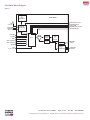
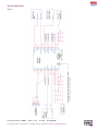
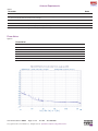
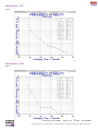
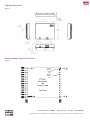
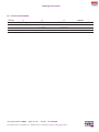
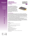
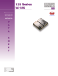
125 Series FTS125
Disciplined Reference and
Synchronous Clock Generator
2111 Comprehensive Drive
Aurora, Illinois 60505
Phone: 630- 851- 4722
Fax: 630- 851- 5040
www.conwin.com
D
A
T
A
S
H
E
E
T
General Description
The FTS125 Frequency and Time Standard module is
a GPS driven, mixed-signal phase lock loop, providing
a 1PPS CMOS output from a Connor-Winfield GPS
timing receiver and generating a 10MHz CMOS and
a 10MHz SINE output from an intrinsically low jitter
voltage controlled crystal oscillator. The FTS125 can
lock to a 10MHz reference derived from the on-board
GPS receiver or an external 10MHz reference or to
an external 1PPS reference. Alarms are provided to
indicate Loss-of-Lock, Holdover, and Antenna Fault. The
on-board GPS receiver requires an outdoor mounted
GPS antenna for the best stability and consistent
performance.
The mode control inputs are used to manually switch
between references and/or holdover. The user application should monitor the alarm outputs
and manually switch modes as needed.
Serial I/O lines provide access to the NMEA messages from the GPS receiver
(referenced in the Connor-Winfield’s Wi125 User Manual. Contact Connor-Winfield Sales
for a copy).The serial I/O lines can be used to access GPS timestamp information, or to
verify that the receiver has recovered from an alarm condition. The reset is used to reset
the GPS receiver (if needed).
Features
•Phase locked 10.0 MHz output
•1 PPS output
•3 selectable references: GPS, External 10MHz or External 1PPS
•Holdover
•Three alarm outputs. (Loss-of-Lock, Holdover and Antenna Fault)
•Serial input and output ports (GPS receiver)
•Master reset
•+3.3 Volt power supply
•Commercial Temp (0-70° C)
•Meets ITU-T G.811 Wander Generation Mask
•Meets ETSI-PRC Wander Generation Mask (with OCXO reference)
•MCX GPS Antenna Connection
•Fixed Position Unit
Bulletin
Page
Revision
Date
Issued By
SG161
1 of 12
00
14 June 10
ENG
Functional Block Diagram
Figure 1
OCXO
or
TCXO
REFERENCE
FTS125 Module
SERIAL OUTPUT (A, B, C)
MCX
Connector
BOOT SEL
HOLDOVER STATUS
LOCK STATUS
ANTENNNA FAULT STATUS
CW25-TIM
(GPS Receiver)
1PPS CMOS OUTPUT
SERIAL IN
(A, B, C)
33Ω
1 pps
∆
GPS REF
10 MHz REF
DPFD
1 PPS REF
RESET
SYNC 1 CONTROL
CPLD
ANALOG
FILTER
LOW JITTER
VCXO
or
OCVCXO
1/N
DRIVER
SYNC 2 CONTROL
33Ω
DISABLE
DRIVER
&
TRANSLATION
JTAG
(Programming Only)
FTS125 Data Sheet #: SG161
Page 2 of 12
10 MHz CMOS
OUTPUT
10 MHz SINE
OUTPUT
Rev: 00
Date: 06/14/10
© Copyright 2010 The Connor-Winfield Corp. All Rights Reserved Specifications subject to change without notice
Typical Application
Figure 2
FTS125 Data Sheet #: SG161
Page 3 of 12
Rev: 00
Date: 06/14/10
© Copyright 2010 The Connor-Winfield Corp. All Rights Reserved Specifications subject to change without notice
Pin Description
Table 1
Pin #
Pin Name
Description
1
TXC
RS-232 communication transmit signal for UART2 (Optional)
2
TXB
RS-232 communication transmit signal for UART1 (Optional)
3
TXA
RS-232 communication transmit signal for UART0 (Optional)
4
GND
5
RXC
RS-232 communication receive signal for UART2 (Optional)
6
RXB
RS-232 communication receive signal for UART1 (Optional)
7
RXA
RS-232 communication receive signal for UART0 (Optional)
8
*Bootsel
9
10MHz Ref Input
10
*Reset
11
GND
12
1PPS Ref Input
13
GND
14
Antenna Supply Voltage
15
GND
16
VCC1
Supply voltage for GPS timing circuitry.
17
VCC2
Supply voltage for noise clean-up and interfacing circuitry. 18
GND
19
SYNC1 Control
Lock mode control signal 1. See Table 4 for functional description. Default state is pulled high internally.
20
SYNC2 Control
Lock mode control signal 2. See Table 4 for functional description. Default state is pulled high internally.
21
*Disable
22
Unused
23
Holdover Status
24
Lock Status
25
Antenna Fault Status
High= A fault has been detected on Pin 14 (Antenna Supply Voltage)
26
1PPS CMOS Output
1PPS CMOS output provided by the CW25-TIM
27
GND
28
10MHz CMOS Output
29
Unused
30
Unused
31
GND
32
10MHz SINE Output
Normally HIGH - Only pulled low for RS-232 re-programming of GPS software. Default state is pulled high internally.
External LVCMOS 10.0MHz reference (Optional). Default state is pulled high internally.
Hardware Reset for the GPS timing circuitry. Pull low to reset. Default state is pulled high internally.
External LVCMOS 1PPS reference (Optional). Default state is pulled high internally.
Antenna Supply Voltage. Limit continuous current to 45mA Max.
Open/High = enabled outputs. Pull low to disable the 10MHz CMOS and SINE outputs. Default state is pulled high internally.
High= Unit is in Holdover
High= Unit is locked to selected reference.
10MHz low jitter CMOS output
10MHz AC coupled low jitter SINE output
FTS125 Data Sheet #: SG161
Page 4 of 12
Rev: 00
Date: 06/14/10
© Copyright 2010 The Connor-Winfield Corp. All Rights Reserved Specifications subject to change without notice
Absolute Maximum Rating
Table 2
Symbol
Parameter
Minimum
Maximum
Units
N otes
VCC
Power Supply Voltage
-0.3
3.7
Volts
1
VIN
Input Voltage
-0.3
4.6
Volts
1
VPREAMP
Antenna Supply Voltage
2.7
13.2
Volts
1
TS
Storage Temperature
-30
80
°C
1
Operating Specifications
Table 3
Symbol
Parameter
Minimum
Nominal
Maximum
Units
VCC1
Supply Voltage 1
ICC1
Supply Current 1
with TCXO (CTV. CST)
with OCXO (COV, COO)
VCC2
Supply Voltage 2
ICC2
Supply Current 2
with VCXO/TCVCXO (COV, CTV, CST)
with VCOCXO (COO)
TO
Temperature Range
tJTOL
tAQ_GPS
tAQ_EXT
3.135
3.3
3.465
V
.200
.480
.300
1.2
A
A
3.135
3.3
3.465
V
2
.038
.380
.060
1.0
A
A
0
70
°C
Input Jitter Tolerance
30
ns
GPS Input Acquisition Time
TCXO
OCXO
120
150
sec
sec
3
3
External Input Acquisition Time
VCXO
OCVCXO
90
120
sec
sec
3
3
PLL Option:
FCAP
Capture/Pull-in Range
Oscillator Performance
VCXO (COV/CTV)
VCTCXO (CST)
OCVCXO (COO)
±50 ppm
±10 ppm
±45 ppb
FBW
Jitter Filter Bandwidth
6 Hz Typ.
0.7 Hz Typ
0.1 Hz Typ.
DC
Duty Cycle
45/55%
45/55
45/55%
RMS
RMS Phase Noise
10Hz - 2MHz 12kHz - 2MHz 20 ps Typ.
0.5 ps Typ.
1.5 ps Typ
0.6 ps Typ
1 ps Typ.
0.6 ps Typ.
Notes
Holdover/Wander Generation Performance
Reference Option:
Int TCXO (CTV)
Ext TCXO (CST)
OCXO (COO, COV)
TSTA
Temperature Stability
±0.5 ppm
±0.28 ppm
±20 ppb
VSTA
Vcc Stability 0.1 ppm
20 ppb
±5 ppb
ADAILY
Daily Aging
-
20 ppb
2 ppb
AYEARLY
Yearly Aging 2 ppm -
80 ppb
Wander Generation Specification
ITU-T G.811
ITU-T G.811
ETSI-PRC
4
5
NOTES:
1. Stresses beyond those listed under “Absolute Maximum Rating” may cause permanent damage to the module. These are stress ratings only and functional operation of the device at these other conditions beyond those indicated under “Operating Specifications” is not implied. Exposure to absolute maximum rated conditions for extended periods may affect device reliability.
2. Requires external regulation and supply decoupling
3. Cold Power-up
4. Holdover will be re-calculated with each successful lock. Yearly aging represents 1 continous year in Holdover.
5. Relative to 25°C
FTS125 Data Sheet #: SG161
Page 5 of 12
Rev: 00
Date: 06/14/10
© Copyright 2010 The Connor-Winfield Corp. All Rights Reserved Specifications subject to change without notice
or any
Mode Control Table
Table 4
* Note: Holdover is not supported in this mode; loss of the 10MHz reference will rail the
PLL output until the reference returns or another mode is selected.
Input And Output Characteristics
Table 5
LVCMOS Inputs and Outputs
Minimum
Maximum
Symbol
Parameter
Units
VIH
High Level Input Voltage
1.7
4.0
V
VIL
Low Level Input Voltage
-0.5
0.8
V
VOH
High Level Output Voltage
2.4
V
VOL
Low Level Output Voltage
0.4
V
CO
Output Capacitance
10
pF
Symbol
Parameter
Load
Output Power
Total Harmonic Distortion
Notes
10MHz Sine Output
Typical
50
9
2.2
Units
Notes
ohms
dBm
%
GPS Receiver Specifications
Table 6
Parameter
Specifications
Acquisition/Tracking Sensitivity
-155dBm/-156dBm
Notes
Acquisition Time:
Hot Start w/ Network Assist Outdoor: <2 sec Indoor(-148dBm) <5 sec
Stand Alone
Supported Protocols
Cold <45 sec Warm: <38 sec
Hot: <5 sec Re-acquisition: <1sec (90% confidendce)
Network Assist, NMEA 0183
Reset Generation (I/O pin 10 - RESET)
The power-on-reset for the FTS125 is generated on-board. If it is desired to extend the power-on-reset signal or provide a manual
reset of the GPS receiver, pull this signal low.
FTS125 Data Sheet #: SG161
Page 6 of 12
Rev: 00
Date: 06/14/10
© Copyright 2010 The Connor-Winfield Corp. All Rights Reserved Specifications subject to change without notice
Antenna Requirements
Table 7
Parameter
Notes
The FTS125 antenna connector is an MCX (female)
The antenna supply voltage provided to Pin 14 must be within the range of 2.7 to 13.2V (AMR); the antenna must be able to operate at this voltage
The antenna’s continuous current draw must be <=45mA
The antenna must have a full sky view for optimal receiver performance
An active antenna with a minimum 10dB gain (including cable loss) should be used
Standard 125 Series models are designed for fixed position operation only. Contact Connor-Winfield Sales for mobile application model offerings
Phase Noise
Figure 2
Phase Noise:
Offset Frequency (Hz)
COO (dBc/Hz)
CST (dBc/Hz)
CTV (dBc/Hz)
10
-105
-90
-70
100
-132
-125
-105
1k
-145
-146
-135
10k
-150
-152
-145
100k
-152
-153
-152
1M
-154
-155
-158
FTS125 Data Sheet #: SG161
Page 7 of 12
Rev: 00
Date: 06/14/10
© Copyright 2010 The Connor-Winfield Corp. All Rights Reserved Specifications subject to change without notice
Allan Variance – CTV
Figure 3
Allan Variance – COO
Figure 4
FTS125 Data Sheet #: SG161
Page 8 of 12
Rev: 00
Date: 06/14/10
© Copyright 2010 The Connor-Winfield Corp. All Rights Reserved Specifications subject to change without notice
Wander Generation Plot – CTV versus G.811 Wander Generation Mask
Figure 5
100,000
10,000
MTIE (ns)
1,000
100
10
1
0.01
0.10
1.00
10.00
100.00
1,000.00
10,000.00
100,000.00
1,000,000.00
Observation Interval (sec)
Wander Generation Plot – COO versus ETSI-PRC Wander Generation Mask
Figure 6
10000
MTIE (ns)
1000
100
10
1
0.1
1
10
100
1000
Observation Interval (sec)
FTS125 Data Sheet #: SG161
Page 9 of 12
Rev: 00
Date: 06/14/10
© Copyright 2010 The Connor-Winfield Corp. All Rights Reserved Specifications subject to change without notice
10000
100000
Package Dimensions
Figure 7
Recommended Footprint Dimensions
Figure 8
0.038"
Hole
Thru All
x32
0.065"
Pad
x32
FTS125
Dimensions
and
Keepout Area
Top View
FTS125 Data Sheet #: SG161
Page 10 of 12
Rev: 00
Date: 06/14/10
© Copyright 2010 The Connor-Winfield Corp. All Rights Reserved Specifications subject to change without notice
Ordering Information
Ex: FTS125-COO-010.0MHz
FTS125
C
Temp Range
O
CW25 Reference
O
PLL Oscillator
C = 0-70degC
O = OCXO
O = OCVCXO *
T = TCXO
V = VCXO
S = Tighter Tolerance TCXO
T = VCTCXO
* CTO Option is not available
FTS125 Data Sheet #: SG161
Page 11 of 12
Rev: 00
Date: 06/14/10
© Copyright 2010 The Connor-Winfield Corp. All Rights Reserved Specifications subject to change without notice
-010.0M Output Frequency
2111 Comprehensive Drive
Aurora, Illinois 60505
Phone: 630- 851- 4722
Fax: 630- 851- 5040
www.conwin.com
Revision
Revision Date
Note
P00
5/12/08
Preliminary Release
P01
6/19/08
Temperature Range Edit
P02
7/17/08
Plots & Graphs added
P03
8/25/08
Acquisition/Tracking Edit
P04
9/15/08
Indoor Temp Revision
P05
11/10/08
MCX Info added & Block Diagram Update
P06
06/30/09
Update for New Model Number
P07
12/10/09
Antenna Requirement & Typ Application Updates
P08
01/08/10
Fixed Unit Clarification & GPS Reference Information
00
06/14/10
125 Series Update and Public Release