1
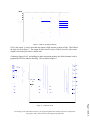
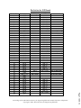
The outputs Y0 – Y7 are used as chip enables signals for addresses 8000H – 8007H. Figure 8
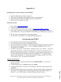
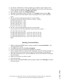
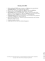
shows the output enables for addresses 8000H – 8002H. Reference “Creating waveforms and test
vectors” Appendix A for waveform simulation. In order to memory map an I/O device to these
addresses, Y0 is then ANDed with the WRITE signal from the micrcontroller to geneartate a
memory WRITE cycle. Y1 can be ANDed with the READ signal from the micrcontroller to
geneartate a memory READ cycle.
Figure 8: Simulation for combined circuit
Conclusion
One method of simplifying hardware circuits in microcontroller labs is to introduce PLDs for
logic design. By using Lattice Semiconductor ispDesignEXPERT software a logic circuit can be
designed and simulated. The simulation capability makes it easier for students to visualize the
timing diagrams of the signals invloved. This helps explain memory mapping I/O devices for
data READ and data WRITE instructions. The logic design are all done in softare which makes
for rapid prototyping as the students troubleshoot their circuits as they design for example an
interface for a liquid crystal display. The use of PLDs also reduces the amount of wirewapping
and increases the reliability of the circuit.
Acknowledgements
The authors would like to thank Mr. Tim Schnettler, Design Tools Marketing Manager with
Lattice Semiconductor Corporation.
Page 7.1059.7
Proceedings of the 2002 American Society for Engineering Education Annual Conference & Exposition
Copyright Ó 2002, American Society for Engineering Education