1
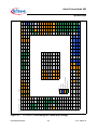
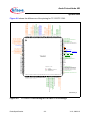
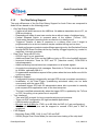
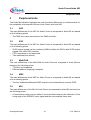
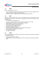
Delta Specification, V1.0, Dec. 2006
Audo Future/Audo NG
32-Bit Single-Chip Microcontroller
Microcontrollers
Edition 2006-12
Published by
Infineon Technologies AG
81726 München, Germany
© Infineon Technologies AG 2006.
All Rights Reserved.
Legal Disclaimer
The information given in this document shall in no event be regarded as a guarantee of conditions or
characteristics (“Beschaffenheitsgarantie”). With respect to any examples or hints given herein, any typical values
stated herein and/or any information regarding the application of the device, Infineon Technologies hereby
disclaims any and all warranties and liabilities of any kind, including without limitation warranties of noninfringement of intellectual property rights of any third party.
Information
For further information on technology, delivery terms and conditions and prices please contact your nearest
Infineon Technologies Office (www.infineon.com).
Warnings
Due to technical requirements components may contain dangerous substances. For information on the types in
question please contact your nearest Infineon Technologies Office.
Infineon Technologies Components may only be used in life-support devices or systems with the express written
approval of Infineon Technologies, if a failure of such components can reasonably be expected to cause the failure
of that life-support device or system, or to affect the safety or effectiveness of that device or system. Life support
devices or systems are intended to be implanted in the human body, or to support and/or maintain and sustain
and/or protect human life. If they fail, it is reasonable to assume that the health of the user or other persons may
be endangered.
Delta Specification, V1.0, Dec. 2006
Audo Future/Audo NG
32-Bit Single-Chip Microcontroller
Microcontrollers
Audo Future/Audo NG Delta Specification
Revision History: V1.0 2006-12
Previous Version: V1.0 is the first released spec version
Page
Subjects (major changes since last revision)
several
see change bars
Trademarks
TriCore™ is a trademark of Infineon Technologies AG.
We Listen to Your Comments
Any information within this document that you feel is wrong, unclear or missing at all?
Your feedback will help us to continuously improve the quality of this document.
Please send your proposal (including a reference to this document) to:
[email protected]
Template: mc_a5_um_tmplt.fm / 4 / 2004-09-15
Audo Future/Audo NG
Table of Contents
Table of Contents
This “Table of Contents” section refers to the page numbers of the Audo Future/Audo
NG Delta Specification.
1
Introduction . . . . . . . . . . . . . . . . . . . . . . . . . . . . . . . . . . . . . . . . . . . . 1-1 [1]
2
2.1
2.2
2.3
2.4
2.5
2.6
2.7
2.8
2.9
2.10
2.11
2.12
2.13
2.14
2.15
System Units . . . . . . . . . . . . . . . . . . . . . . . . . . . . . . . . . . . . . . . . . . . 2-1 [1]
Pinning . . . . . . . . . . . . . . . . . . . . . . . . . . . . . . . . . . . . . . . . . . . . . . . . . 2-1 [1]
CPU . . . . . . . . . . . . . . . . . . . . . . . . . . . . . . . . . . . . . . . . . . . . . . . . . . . 2-4 [1]
SCU . . . . . . . . . . . . . . . . . . . . . . . . . . . . . . . . . . . . . . . . . . . . . . . . . . . 2-5 [1]
On-Chip System Buses and Bus Bridges . . . . . . . . . . . . . . . . . . . . . . 2-6 [1]
PMU . . . . . . . . . . . . . . . . . . . . . . . . . . . . . . . . . . . . . . . . . . . . . . . . . . . 2-7 [1]
Data Access Overlay . . . . . . . . . . . . . . . . . . . . . . . . . . . . . . . . . . . . . . 2-8 [1]
BootROM . . . . . . . . . . . . . . . . . . . . . . . . . . . . . . . . . . . . . . . . . . . . . . . 2-9 [1]
Memory Maps . . . . . . . . . . . . . . . . . . . . . . . . . . . . . . . . . . . . . . . . . . . 2-9 [1]
GPIO Ports and Peripheral I/O . . . . . . . . . . . . . . . . . . . . . . . . . . . . . 2-10 [1]
PCP . . . . . . . . . . . . . . . . . . . . . . . . . . . . . . . . . . . . . . . . . . . . . . . . . . 2-10 [1]
DMA . . . . . . . . . . . . . . . . . . . . . . . . . . . . . . . . . . . . . . . . . . . . . . . . . . 2-11 [1]
EBU . . . . . . . . . . . . . . . . . . . . . . . . . . . . . . . . . . . . . . . . . . . . . . . . . . 2-12 [1]
Interrupt System . . . . . . . . . . . . . . . . . . . . . . . . . . . . . . . . . . . . . . . . 2-13 [1]
System Timer . . . . . . . . . . . . . . . . . . . . . . . . . . . . . . . . . . . . . . . . . . . 2-13 [1]
On-Chip Debug Support . . . . . . . . . . . . . . . . . . . . . . . . . . . . . . . . . . 2-14 [1]
3
3.1
3.2
3.3
3.4
3.5
3.6
3.7
3.8
3.9
Peripheral Units . . . . . . . . . . . . . . . . . . . . . . . . . . . . . . . . . . . . . . . . .
ASC . . . . . . . . . . . . . . . . . . . . . . . . . . . . . . . . . . . . . . . . . . . . . . . . . . .
SSC . . . . . . . . . . . . . . . . . . . . . . . . . . . . . . . . . . . . . . . . . . . . . . . . . . .
MultiCAN . . . . . . . . . . . . . . . . . . . . . . . . . . . . . . . . . . . . . . . . . . . . . . .
MSC . . . . . . . . . . . . . . . . . . . . . . . . . . . . . . . . . . . . . . . . . . . . . . . . . . .
MLI . . . . . . . . . . . . . . . . . . . . . . . . . . . . . . . . . . . . . . . . . . . . . . . . . . . .
GPTA . . . . . . . . . . . . . . . . . . . . . . . . . . . . . . . . . . . . . . . . . . . . . . . . . .
ERAY . . . . . . . . . . . . . . . . . . . . . . . . . . . . . . . . . . . . . . . . . . . . . . . . . .
ADC . . . . . . . . . . . . . . . . . . . . . . . . . . . . . . . . . . . . . . . . . . . . . . . . . . .
FADC . . . . . . . . . . . . . . . . . . . . . . . . . . . . . . . . . . . . . . . . . . . . . . . . . .
Delta Specification
I-1
3-1 [2]
3-1 [2]
3-1 [2]
3-1 [2]
3-1 [2]
3-1 [2]
3-2 [2]
3-4 [2]
3-4 [2]
3-4 [2]
V1.0, 2006-12
Audo Future/Audo NG
1
Introduction
Introduction
The Delta Specification highlights the main functional differences or enhancements
between Infineon Audo Future and Audo NG.
The reference documents for this document are:
•
•
•
•
•
•
•
TC1797 Target Specification, V1.2, Dec. 2006
TC1767 Target Specification, V1.2, Dec. 2006
TC1796 System and Peripheral Units User’s Manual (Vol.1 and 2), V1.0, June 2005
TC1796 Documentation Addendum, V1.1, Sept. 2006
TC1766 System and Peripheral Units User’s Manual (Vol.1 and 2), V1.1, Aug.2005
TC1766 Documentation Addendum, V1.1, Oct. 2006
Errata Fix Matrix, TC1796_BE_TC1797_bugfix_V13_external.xls
Delta Specification
1-1
V1.0, 2006-12
Audo Future/Audo NG
2
System Units
System Units
This section highlights the main functional differences or enhancements for the system
units between Infineon Audo Future and Audo NG.
2.1
Pinning
Figure 2-1 shows the differences of the pinning for TC1797/TC1796:
Delta Specification
2-1
V1.0, 2006-12
Figure 2-1
Delta Specification
2-2
AN6
AD
AN33
AN1
AN4
2
AN8
AC
AN9
1
AN12
AB
AN11
AN37
AN15
AA
AN14
AN17
AN0
AN18
Y
N.C.
AN20
W
P7.7
AN21
AF
AN22
V
P7.5
P7.1
P1.1
P1.7
P1.9
P6.13
P6.10
P6.11
P2.3
3
AN39
AN36
AN34
AN32
AN3
AN5
AN10
AN13
AN19
P7.3
P7.4
P7.0
P1.0
P1.6
P1.8
P1.13
P8.6
P8.2
VDDFL3
P6.7
P6.4
P6.6
P2.2
P2.11
P2.10
P2.13
Topview
4
AN43
AN41
AN40
AN38
AN7
AN2
VSSM
VDDM
AN16
P7.2
VSS
VDD
P1.12
P1.4
P1.5
P1.11
VDDP
VSS
VDD
P6.5
P6.8
P6.9
P0.15
P2.12
P2.14
P2.15
5
VAGND0
VAREF0
AN35
AN42
P0.13
P0.12
P0.9
P0.14
6
AN29
AN28
VAREF1
VAGND1
green
orange
blue
grey
VDDP
P0.8
P0.4
P0.2
VSS
P0.7
P0.3
P0.1
P0.0
VDD
P3.7
P3.15
VSS
VSS
VSS
VSS
VSS
VSS
VSS
VSS
P3.8
P3.10
P3.6
P3.14
7
AN31
AN30
AN27
AN26
8
VFAREF
VFAGND
AN25
AN24
VDDAF
9
VSSMF
VDDMF
VAREF2
additional functions
10
P4.6
P4.1
P4.0
VSS
changed or removed functions
port-mapped
no change
Legend:
P0.11
P0.10
P0.6
P0.5
Version 1.2
11
P4.9
P4.3
P4.2
VDD
VSS
VSS
VSS
VSS
VSS
VSS
VSS
VSS
P3.12
P3.9
P3.3
P3.5
12
P4.10
P4.7
P4.5
P4.4
VSS
VSS
VSS
VSS
VSS
VSS
VSS
VSS
P3.13
P3.4
P3.0
P3.1
13
P4.14
P4.13
P4.11
P4.8
VSS
VSS
VSS
VSS
VSS
VSS
VSS
VSS
P3.11
P3.2
P5.0
P5.1
14
P10.3
P10.4
P4.15
P4.12
VSS
VSS
VSS
VSS
VSS
VSS
VSS
VSS
VDDP
P5.5
P5.3
P5.2
15
P10.1
P10.0
P10.2
P10.5
VSS
VSS
VSS
VSS
VSS
VSS
VSS
VSS
VSS
P5.4
P5.6
P5.7
16
VDDP
VDDP
VDDP
VDDP
VSS
VSS
VSS
VSS
VSS
VSS
VSS
VSS
VDD
P5.9
P5.13
P5.12
17
P16.0
P15.4
P15.5
VSS
VSS
VSS
VSS
VSS
VSS
VSS
VSS
VSS
P5.8
P5.10
P5.14
P5.15
18
P15.6
P15.7
P16.1
VDDEBU
P9.4
P5.11
VDDFL3
VDDFL3
19
P15.12
P16.3
P15.3
VSS
P9.5
P9.6
P9.1
P9.0
20
P15.8
P15.11
P15.2
VDD
P9.7
P9.8
P9.2
P9.3
P9.9
21
P15.9
P15.0
P15.1
N.C.
P9.12
P9.11
P9.10
ESR1
22
P15.10
N.C.
P16.2
VDDEBU
VDDP
N.C.
PORST
ESR0
23
P15.13
N.C.
N.C.
VSS
VDD
P14.3
VDDEBU
VSS
VDD
P13.6
VDDEBU
VSS
VDD
P11.13
VDDEBU
VSS
P11.7
P11.3
VDDEBU
VDDPF
TRST
VDD
VSS
VDDP
TESTMODE
N.C.
24
P15.14
P14.14
P14.15
P14.12
P14.5
P14.6
P14.2
P14.0
P13.13
P13.9
P13.1
P12.3
P12.1
P11.14
P11.10
P11.11
P11.4
P12.6
VDDEBU
VDDPF3
TMS
TCK
VDD
VSS
VDDP
25
P15.15
P14.13
P14.11
P14.9
P14.4
P14.1
P13.14
P13.12
P13.8
P13.5
P13.3
P12.5
P12.2
P11.15
P11.9
P11.5
P11.1
P12.7
VDDEBU
XTAL2
VSSOSC
TDI
TDO
VDD
VSS
VDDP
VSS
26
N.C.
P14.10
P14.8
P14.7
P13.15
P13.11
P13.10
P13.7
P13.4
P13.2
P13.0
P12.4
P12.0
P11.12
P11.8
P11.6
P11.2
P11.0
VDDEBU
XTAL1
VDDOSC
VDDOSC3
P9.14
P9.13
VDD
AE
AN23
U
P1.10
P7.6
P1.15
L
M
VDDE(sb)
P8.7
T
P8.4
J
K
R
P8.1
H
P1.2
P1.14
P6.15
G
P1.3
P8.5
P6.14
F
P
P8.3
P6.12
E
N
P8.0
P2.4
D
P2.8
P2.5
C
P2.7
P2.9
P2.6
N.C.
B
A
Changes to TC1796
Audo Future/Audo NG
System Units
TC1797/TC1796 Pinning for P-BGA-416 Package
V1.0, 2006-12
AN1 9
AN1 8
AN1 7
AN1 6
AN1 5
AN1 4
VAGND0
VAREF0
V SSM
V DDM
AN1 3
AN1 2
AN1 1
AN1 0
A N9
A N8
A N6
A N5
A N4
A N3
A N2
A N1
A N0
V DD
VDDP
VSS
A D0E M UX2 /OUT 18/IN1 8/P 1.1 4
A D0E M UX1 /OUT 17/IN1 7/P 1.1 3
A D0E M UX0 /OUT 16/IN1 6/P 1.1 2
TCLK 0 /OUT2 8/OUT 32/ IN32/P 2. 0
SL SO 13/S LS O0 3/OUT 33/ TRE A DY0 A/ IN33/P 2. 1
T VA LID0 A /OUT2 9/OUT 34/ IN34/P 2. 2
TDA TA 0 /OUT3 0/OUT 35/ IN54/P 2. 3
O UT31 /OUT 36/RCL K0 A/ IN36/P 2. 4
RRE ADY 0A /O UT37 /OUT 110/ IN37/P 2. 5
OUT 38 /OUT1 11/RV A LID0 A/ IN38/P 2. 6
OUT 39/RDA T A0 A/ IN39/P 2. 7
VSS
VDDP
V DD
VSS
OUT 52/OUT 28 /IN52/ IN28/P 4. 0
OUT 53/OUT 29 /IN53/ IN29/P 4. 1
E X TCL K1 /OUT 54/OUT 30 /IN54/ IN30/P 4. 2
45
46
47
48
49
50
51
52
53
54
55
56
57
58
59
60
61
62
63
64
65
66
67
68
69
70
71
72
73
74
75
76
77
78
79
80
81
82
83
84
85
86
87
88
OUT 40/OUT 8/IN40/IN26/P5.0
OUT 41/OUT 9/IN41/IN27/P5.1
OUT 42/OUT 10/IN42/IN28/P5.2
OUT 43/OUT 11/IN43/P5.3
OUT 44/OUT 12/IN44/IN29/P5.4
OUT 45/OUT 13/IN45/IN30/P5.5
OUT 46/OUT 14/IN46/IN31/P5.6
OUT 47/OUT 15/IN47/P5.7
T CLK0/OUT 95/P5.15
VDD
V DDP
V SS
RDAT A0B/OUT 89/P5.8
RVALID0B/OUT 90/P5.9
RREADY0B/OUT 91/P5.10
RCLK0B/OUT 92/P5.11
T DAT A0/SLSO07/OUT 93/P5.12
T VALID0B/SLSO16/P5.13
T READY0B/OUT 94/P5.14
V DDP
V
DD(SB)
V
SS
V DDAF
VDDMF
V
SSMF
VFAREF
V FAGND
AN35
AN34
AN33
AN32
AN31
AN30
AN29
AN28
AN7
AN27
AN26
AN25
AN24
AN23
AN22
AN21
AN20
Figure 2-2
Delta Specification
1
2
3
4
5
6
7
8
9
10
11
12
13
14
15
16
17
18
19
20
21
22
23
24
25
26
27
28
29
30
31
32
33
34
35
36
37
38
39
40
41
42
43
44
17 6
17 5
17 4
17 3
172
171
170
169
168
167
166
16 5
16 4
16 3
162
161
160
159
158
157
156
155
154
153
15 2
15 1
15 0
14 9
14 8
147
14 6
14 5
14 4
14 3
14 2
14 1
14 0
13 9
13 8
137
13 6
13 5
13 4
13 3
P 0. 15/I N15/RE Q5/ OUT1 5/OUT 71
P 0. 14/I N14/RE Q4/ OUT1 4/OUT 70
P 0. 7/IN7 /HW CFG7 /REQ 3/OUT 7/OUT 63
P 0. 6/IN6 /HW CFG6 /REQ 2/OUT 6/OUT 62
V SS
V DDP
V DD
P 0. 13/I N13/OUT 13 /OUT6 9
P 0. 12/I N12/OUT 12 /OUT6 8
P 0. 5/IN5 /HW CFG5 /OUT5 /OUT 61
P 0. 4/IN4 /HW CFG4 /OUT4 /OUT 60
P 2. 13/I N13/OUT 3/S LS I1 1/S DI0
P 2. 8/S LS O04 /S LS O14/ EN0 0
P 2. 12/I N12/OUT 2/M TS R1A /S OP 0B
P 2. 11/I N11/OUT 1/S CLK 1A /F CLP 0B
P 2. 10/I N10/OUT 0/M RS T1A
P 2. 9/S LS O05 /S LS O15/ EN0 1
P 6. 3/IN2 5/OUT 7/OUT 83/ SO P0 A
P 6. 2/IN2 4/OUT 6/OUT 82/ SO N0
P 6. 1/IN1 5/OUT 5/OUT 81/ FCLP 0A
P 6. 0/IN1 4/OUT 4/OUT 80/ FCLN0
V SS
V DDP
V DD
P 0. 11/I N11/OUT 11 /OUT6 7
P 0. 10/I N10/OUT 10 /OUT6 6
P 0. 9/IN9 /OUT9 /OUT 65
P 0. 8/IN8 /OUT8 /OUT 64
P 0. 3/IN3 /HW CFG3 /OUT3 /OUT 59
P 0. 2/IN2 /HW CFG2 /OUT2 /OUT 58
P 0. 1/IN1 /HW CFG1 /OUT1 /OUT 57
P 0. 0/IN0 /HW CFG0 /OUT0 /OUT 56
P 3. 11/O UT93 /RE Q1
P 3. 12/O UT94 /RX DCAN0 /RXD0 B
P 3. 13/O UT95 /TX DCA N0/T X D0
V DDFL3
V SS
V DDP
P 3. 9/OUT 91/ RXD1 A
P 3. 10/O UT92 /RE Q0
P 3. 0/OUT 84/ RXD0 A
P 3. 1/OUT 85/ TX D0
P 3. 14/O UT96 /RX DCAN1 /RXD1 B
P 3. 15/O UT97 /TX DCA N1/T X D1
Audo Future/Audo NG
System Units
Figure 2-2 shows the differences of the pinning for TC1767/TC1766:
TC1767
Changes from T C1766:
grey
blue
orange
green
2-3
no change
port-m apped
changed or rem oved functions
additional functions
132
131
130
129
128
127
126
125
124
123
122
121
120
119
118
117
116
115
114
113
112
111
110
109
108
107
106
105
104
103
102
101
100
99
98
97
96
95
94
93
92
91
90
89
P3.4/OUT 88/MT SR0
P3.7/SLSI01/OUT 89/SLSO02/SLSO12
P3.3/OUT 87/MRST 0
P3.2/OUT 86/SCLK0
P3.8/SLSO06/OUT 90/T XD1
P3.6/SLSO01/SLSO11/SLSO01&SLSO11
P3.5/SLSO00/SLSO10/SLSO00&SLSO10
V
SS
VDDP
VDD
ESR0
PORST
ESR1
P1.1/IN17/OUT 17/OUT 73
T EST MODE
P1.15/BRKIN/BRKOUT
P1.0/IN16/OUT 16/OUT 72/BRKIN/BRKOUT
T CK/DAP0
T RST
T DO/DAP2/BRKIN/BRKOUT
T MS/DAP1
T DI/BRKIN/BRKOUT
P1.7/IN23/OUT 23/OUT 79
P1.6/IN22/OUT 22/OUT 78
P1.5/IN21/OUT 21/OUT 77
P1.4/IN20/EMGST OP/OUT 20/OUT 76
VDDOSC3
VDDOSC
VSSOSC
XT AL2
XT AL1
V
SS
VDDP
V
P1.3/IN19/OUT 19/OUT 75
P1.11/IN27/IN51/SCLK1B/OUT 27/OUT 51
P1.10/IN26/IN50/OUT 26/OUT 50/SLSO17
P1.9/IN25/IN49/MRST 1B/OUT 25/OUT 49
P1.8/IN24/IN48/MT SR1B/OUT 24/OUT 48
P1.2/IN18/OUT 18/OUT 74
V SS
V DDP
P4.3/IN31/IN55/OUT 31/OUT 55/EXT CLK0
V DD
DD
MCP06067_d
TC1767/TC1766 Pinning for PG-LQFP-176-x Package
V1.0, 2006-12
Audo Future/Audo NG
System Units
2.2
CPU
The main differences of the CPU for Audo Future as compared to Audo NG are based
on the following points:
•
•
•
•
•
•
•
•
•
•
•
•
•
•
TriCore 1.3.1 is User mode backwards compatible to TC1.3. The cycle timing may
change slightly due to microarchitectural performance improvements.
Backwards-compatible from the Supervisor mode perspective, except for the FPU
interrupt which turned into an CAE trap (trap vector table instead of interrupt vector
table).
Introduction of a 128-bit Data Line Buffer within LMB interface of DMI, increasing
performance of accesses to cacheable addresses.
Enhanced Data Cache manipulation support with the introduction of new DCACHE
instructions CACHEI.W (Cache Index, Write Back) & CACHEI,WI (Cache Index,
Write Back, Invalidate).
Improved instruction fetch system with small dynamic branch predictor. The usage of
old/new branch prediction behavior can be selected via a control register bit.
Improved debug support including upgraded OCDS Level 3 trace port and
performance counters. Dedicated performance counters capture CPU clocks,
Instruction Count, Instruction Cache Hit/Miss and Data Cache Hit/Miss (clean or
dirty).
Increased flexibility in the system address map. PMI Sratchpad SRAM is relocated
from C4000000H to C0000000 H in order to support absolute addressing within the
first 16 KByte.
Improved Floating-Point Unit supporting flexible C compatible conversion functions
and improved exception handling. The usage of old/new FPU behavior can be
selected via control register bit.
Faster Integer MAC/MUC execution unit (all instructions have single-cycle repeat
rate and a latency of 2).
Reduced TriCore Power Consumption.
Introduction of Data Cache.
Configurable size of Instruction Cache and Data Cache.
Byte write support from LMB to SPRAM.
Removed DMI data input register stage between LMB and DMI data input.
Delta Specification
2-4
V1.0, 2006-12
Audo Future/Audo NG
System Units
2.3
SCU
The main differences of the SCU for Audo Future as compared to Audo NG are based
on the following points:
•
•
•
•
•
•
•
•
•
•
•
•
•
•
•
•
•
•
The Clock Generation Unit consists of the oscillator circuit, PLL and an additional
Clock Control Unit. It provides clocks which can configured accordingly.
2 external clock outputs pins are available.
Hardware support for GPTA counter to detect an up-and-stable crystal.
Oscillator Run Detection includes an Oscillator Watchdog which monitors the input
frequency where the expected input frequency is configurable.
During PLL VCO Loss-of-Lock event, the oscillator can be configured to remain
connected to the VCO.
Two K-dividers are available, K1 is defined for Normal and Freerunning Mode and K2
for Prescaler Mode.
New reset model for power-on reset, system reset, debug reset and application reset
and EEC reset.
Reset counters ensures a configurable minimum length of reset.
Reset triggers lead to specific, configurable or no reset.
Only 10 pins are needed for boot option control.
ESR pins are introduced to trigger a reset, a trap (NMI), a reset output or as data pin.
Die temperature sensor is independent from other internal resources (ADC) and no
specific power supply is needed.
Enhanced debug support for the Watchdog Timer.
FPU interrupts are no longer processed in the SCU where they are shifted to CPS.
Flexible interrupt and trap handling in the SCU.
Pad Test Mode is replaced by boundary scan.
Pad Driver Temperature Compensation Control is removed.
EBU pull-up control is performed through the port control.
Delta Specification
2-5
V1.0, 2006-12
Audo Future/Audo NG
System Units
2.4
On-Chip System Buses and Bus Bridges
The main differences of the On-Chip System Buses and Bus Bridges for Audo Future as
compared to Audo NG are based on the following points:
•
•
•
•
•
•
•
•
•
•
The Audo Future is based on two on chip busses (LMB , SPB). The remote peripheral
bus (RPB) is removed.
The DMA is additionally connected to the LMB bus with a master interface.
In TC1797, the Flexray module is additionally connected to the SPB with a slave
interface.
The OCDS module is connected to the DMA. The OCDS module has direct access
to the LMB/SPB bus via the DMA-LMB and DMA-SPB master interface.
DMA decides to forward transactions from DMA internal sources (Move Engine 0/1,
MLI0/1 and Cerberus) to LMB/SPB by internal address decoding.
The DMA controller can generate single data read and write transactions on the LMB
bus. The DMA does not forward directly transactions from the FPI bus to the LMB bus
or vice versa (no LMB<->FPI bridge functionality). Further DMA details and/or DMA
changes compared to AudoNG can be found in the DMA chapter.
The DMA module is now able to access the LMB / SPB bus with three priorities.
Priority of DMA access is controlled by the OCDS (for DMA-OCDS accesses) and by
the Move Engine Channels for DMA-Move Engine accesses.
The LMB-to-FPI bridge (LFI) address translation table was adapted to the
AudoFuture address space.
A new SBCU_DBDAT register is introduced for enhanced OCDS Level 1.
The table On Chip Bus Master TAG Assignments is adapted.
Delta Specification
2-6
V1.0, 2006-12
Audo Future/Audo NG
System Units
2.5
PMU
The main differences of the PMU for Audo Future as compared to Audo NG are based
on the following points:
•
•
•
•
•
•
•
•
•
•
•
•
•
•
•
•
•
•
•
With an additional 2 MByte Flash module in TC1797, concurrent write and read
operations are supported with both Flash modules (2 x 2Mbyte).
Sectorization is changed where each 512 KByte sectors (the 480 KByte sector in
TC1766 inclusive) in PFlash is replaced by 2x256 KByte sectors. The 128 KByte
sector for 8 logical sectors (only in TC1766) is replaced by 2x64 Kbyte sectors.
Read protection can be excluded for Data Flash in Audo Future.
Verify and operation error interrupt can be generated in Audo Future.
Wait states for read access to PFlash and DFlash is supported up to fifteen clock
cycles in Audo Future as compared to seven clock cycles in Audo NG.
The FSI recovery is fully controlled by the FSI in Audo Future/TC1766 as compared
to the control by PMU in TC1796.
Dynamic power reduction where idle states can be used to disable the wordline
drivers in PFlash.
A wordline in PFlash can also be invalidated in addition to invalidation stamp of only
DFlash.
The Flash interrupt control register is located in the SCU for Audo Future as
compared to the location in the DMA controller in Audo NG.
If read protection is active in Audo Future, the user has to install the SPR/cache
configuration after reset to lock the configuration (enable protection) to disable data
read accesses to the instruction cache. If read protection is active in Audo NG, any
data read access to the instruction cache is disabled after reset by the dedicated
logic.
If page buffer is not full, sequence error can be generated with Write Page command.
Global sleep request from SCU is supported.
PFlash instruction access (inclusive of non-cached mode) is four double-word bursts.
For cached data read access to the Program Flash in Audo Future, the transfer of the
aligned two double-word block starts with the critical(addressed) double-word
compared to the lowest double-word of the TC1796.
Direct Flash read access from Debug Interface is improved as there is no LFI bridge
delay and same addressing as CPU side.
OVRAM is parity-protected.
In Emulation Device, base address of 256 Kbyte EMEM is identical to the 512 Kbyte
base address.
New OLDA function with virtual memory range in PMU for callibration data acquisition
and for redirection to overlay memory. New OVRCON register in PMU.
Overlay function control is located in DMI for Audo Future as compared to the control
in PMU in Audo NG.
Delta Specification
2-7
V1.0, 2006-12
Audo Future/Audo NG
System Units
2.6
Data Access Overlay
The main differences of the Data Access Overlay for Audo Future as compared to Audo
NG are based on the following points:
•
•
•
•
•
•
•
•
•
•
•
•
All OVC register addresses are shifted into the CPU space.
A virtual memory range provided in PMU can be additionally used for redirection to
overlay memory.
If the chip is an emulation device, the external memory can also be used as overlay
memory.
All configured overlay blocks can be enabled or disabled with one register access, a
set of overlay blocks can be exchanged with another set of prepared blocks in one
step.
Programmable flush (invalidate) control for data cache in DMI is available in Audo
Future.
Overlay configured status bit can be set when overlay registers are configured by the
Cerberus via JTAG interface. This bit can be used as handshake signal for
Cerberus/CPU to start the prepared overlay blocks.
New OCON register for control of overlay functions.
Minimum overlay block size increased to 16 Bytes in Audo Future as compared to 2
in Audo NG. Additional block sizes in OVRAM of 1KByte and 2 KByte.
Additional sizes of overlay blocks of 64 KByte and 128 KByte in EMEM.
All EMEM block sizes are supported for external overlay memory.
Flash size above 2 MByte is supported for overlay control.
Support of different overlay memory selections for every enabled memory block in
Emulation Device.
Delta Specification
2-8
V1.0, 2006-12
Audo Future/Audo NG
System Units
2.7
BootROM
The main differences of the BootROM content for Audo Future as compared to Audo NG
regarding the device boot-operation (controlled by the Startup Software) from user point
of view are based on the following points:
•
•
The Startup mode selection is done by
– Audo Future - between 2 (for Internal Start) and 8 (for External Start modes) P0
pins (out of P0[7:0])
– Audo NG - HWCFG[3:0] + SWOPT[7:0] + BRKIN (a total of 12 pins)
Bootstrap Loader via CAN pins can use either ASC or CAN protocol; the exact type
of communication protocol is
– Audo Future - automatically detected by the Startup Software
– Audo NG - selected via configuration pins.
2.8
Memory Maps
The general target for the Audo Future devices is to keep the address map compatible
with the Audo NG devices where ever possible. As a result, most of the start addresses
of the SRAMs, Flash segments and the peripheral control register sets of TC1767 and
TC1797 are identical to TC1766 and TC1796, respectively. The main differences of the
memory map for Audo Future as compared to Audo NG are based on the following
points:
•
•
•
•
•
•
•
•
•
•
•
•
•
Address map is adapted to the peripheral set of the products (peripherals where
added/removed, number of ports is adapted).
Target was to keep the start address where possible of all common modules, SRAMs
and Flash segments.
Added PMI Byte Read/Write access.
Added Double-Word support for PCP-CRAM and PCP-PRAM accesses where CPU
has also 64 bit access to the PCP memories.
Moved SCU address map inside Segment 15 as SCU requires 2x256Byte in Audo
Future.
Moved ADC and FADC address maps inside Segment 15 as these modules require
more 256 byte slices in Audo Future.
Adapted memory and flash sizes (SPRAM, LDRAM, CRAM, PRAM, PFlash, DFlash)
OVRAM is moved from Segment 12 to Segment 8 and Segment 10.
Emulation Device Memory was moved from xFF2-0000 -> xFF5FFF to xFF0-0000 > xFF3-FFFF.
An PMI memory mirror image was added (SPRAM + configurable ICACHE) to C000.
Added map of the mirrored PMI memory image to segment E800.
Removed Boot ROM Address Space in segment D as it is not necessary any more
in Audo Future.
Added Online Data Acquisition Address Space (OLDA) to segment 8 and A.
MultiCAN module address space increased from 8KB -> 16KB.
Delta Specification
2-9
V1.0, 2006-12
Audo Future/Audo NG
System Units
•
Changed the SPB view of segment C and D in a way that it is now fully transparent
(write accesses to reserved addresses result in LMBBE, read to SPBBE & LMBBE)
Added Overlay Control Module (OVC) with 256 byte to segment 15 as this
functionality is moved now to DMI.
•
2.9
GPIO Ports and Peripheral I/O
The main differences of the GPIO ports and peripheral I/O for Audo Future as compared
to Audo NG are based on the following points:
•
The EBU signals are controlled in the ports. The hardware-controlled signals override
the priority of the software-configured port pin direction (input or output) and signal
source (EBU or Alternate Outputs).
2.10
PCP
The main differences of the PCP for Audo Future as compared to Audo NG are based
on the following points:
•
•
•
Enhanced PCP core to support higher clock frequencies.
Multiple clock ratios PCP:FPI 1:1 and 2:1.
Improvement of PCP Trace Interface to MCDS.
Delta Specification
2-10
V1.0, 2006-12
Audo Future/Audo NG
System Units
2.11
DMA
The main differences of the DMA for Audo Future as compared to Audo NG are based
on the following points:
•
•
•
•
•
•
•
•
•
•
•
A new mode for the shadow address register was introduced to support endless
channel re-starts without CPU intervention. In this new mode, the shadow address
register can be written directly and it is not re-set automatically when loaded into
target or destination address register. The new Shadow Register Write Enable bit
was added to the register DMA_ADRCR1/0x.
The DMA channels are supporting now transactions with data moves > 32 KB (bit
fields CHCR.TREL and CHSR.TCOUNT are extended to 10 bit.
As a central module of the AudoFuture system on chip architecture, the DMA is now
directly connected to the LMB with an own LMB master interface. The DMA master
interface to the RPB was removed as the AudoFuture system architecture is based
on a single LMB and single FPI (SPB) bus.
The RPB BCU control registers were removed as there is no remote peripheral bus
in AudoFuture.
The Cerberus module is now connected to the DMA Peripheral Interface. This
enables the Cerberus module to have direct access to the FPI and to the LMB bus
via the DMA master interfaces either with the highest or with the lowest priority on
LMB / FPI.
3-level programmable priority of the DMA Sub-Block at the on chip bus interfaces (2level in AudoNG). The bit field DMAPRIO is expanded to 2 bits in the Channel Control
register to support the three DMA on chip bus priorities. The new structure is on the
one hand compatible to the AudoNG channel priorities on the SPB, on the other hand
it allows to use DMA channels for low priority background tasks on LMB like memory
scrubbing. Additionally the DMA On Chip Bus priorities and the DMA bus switch
priorities are adapted.
The System Interrupt Registers are removed from the DMA module (moved to CPU
PMU and SCU).
The DMA module has 8 Service Requests nodes. DMA interrupt outputs DMA
SR[7:0] are connected to interrupt nodes. SR[15:8] are used as DMA channel
request inputs (DMA_SRCn (n = 0-7)).
Up to 16 selectable request inputs per DMA channel (up to 8 in Audo NG). To allow
a more flexible usage of the Move Engine Channels, the number of channel request
inputs was increased to 16 (DMA_CHRC0x/1x.PRSEL expanded from 3 bit to 4 bit,
and the DMA request wiring matrix was re-defined.
Adapted the DMA access protection assignment to the Audo Future address map
The address protection sub-ranges are mapped to OVRAM, LDRAM, SPRAM and
PCP PRAM.
In general the DMA control registers where adapted to the new structure in Audo
Future (one FPI master interface and one LMB master interface instead of two FPI
master interfaces).
Delta Specification
2-11
V1.0, 2006-12
Audo Future/Audo NG
System Units
2.12
EBU
The main differences of the EBU for Audo Future as compared to Audo NG are based
on the following points:
•
•
•
•
•
•
•
•
•
•
•
Registers remapped to simplify programming. A region can now be reconfigured with
a single write.
Each region can now have different settings for read and write accesses. This
enables a region to be configured for synchronous, burst reads and asynchronous
writes. This improves support for burst flash memories.
Access latency when using the gated burst flash clocking mode has been reduced by
two BFCLKO cycles.
Prefetch buffer has been removed, along with byte addresses on the external bus
(i.e. the previously implemented BUSCON.AALIGN bit is now permanently active)
and big-endian support. 1)
Access pipelining has been improved, allowing increased utilisation of the external
bus.
New feature, "chip select locking" added to simplify burst flash programming.
Unused EBU pads are now available for use as GPIO.
1:3 clock mode for generating BFCLKO now results in a clock with a 50% duty cycle.
EBU clock can now be disabled if the EBU is not required for a significant time period.
Automatic wakeup when accessed
Support for industrial memories updated. Improved support for SSRAM, PSRAM and
NAND flash memory types.
EBU supports 16-bit multiplexed mode now.
1) As BUSCON.AALIGN bit has been removed, due to compatibility mode after reset for PCB design, a ballout
change have been implemented (A0 ← A22, A1 ← A23, A2 ← A0, A3 ← A1, …) in order to support combi
layouts for TC1796 and TC1797 derivatives in BGA416 package in combination with 32-bit external memory
devices.
Delta Specification
2-12
V1.0, 2006-12
Audo Future/Audo NG
System Units
2.13
Interrupt System
The main differences of the interrupt system for Audo Future as compared to Audo NG
are based on the following points:
•
The System Interrupt Registers are moved from DMA module to CPU, PMU and SCU
modules.
2.14
System Timer
The main differences of the system timer for Audo Future as compared to Audo NG are
based on the following points:
•
•
The STM registers can be excluded from application reset if configured.
The 2 service request outputs are additionally connected to ADC and DMA modules
and allow triggering requests in these modules.
Delta Specification
2-13
V1.0, 2006-12
Audo Future/Audo NG
System Units
2.15
On-Chip Debug Support
The main differences of the On-Chip Debug Support for Audo Future as compared to
Audo NG are based on the following points:
•
•
•
•
•
On-Chip Debug Support
– Cerberus has direct access to the LMB bus. No address translation due to LFI, no
SPB bus blocking.
– Requesting all kinds of reset can now be done without usage of sideband pins.
– Central Suspend Switch to suspend parts of the system (TriCore, PCP,
Peripherals) instead if breaking them as reaction to a debug event.
– Triggered Transfer of data in response to a debug event now if target is
programmed to be a device interface simple variable tracing can be done.
– In depth performance analysis and profiling support given by the Emulation Device
through MCDS Event Counters driven by a variety of trigger signals (e.g. cache hit,
wait state, interrupt accepted).
Real Time Trace with ED only
– OCDS Level 2 is not supported.
– Additional Data Flow Trace on the LMB bus (only on FPI in the AudoNG devices).
– Improved Instruction Trace for PCP and TC (‘’absolute mode”). PSW.PRS is
traced separately.
– Additional debug events based on comparators on all traced signals.
– Accurate time stamping of all messages. Resolution is TriCore clock rate now up
to 80 MHz, optionally half of it.
– Programmable automatic suspend of the system when the trace buffer runs full for
continuous trace.
Calibration Support
– Configuration change is triggered by a single SFR access to maintain consistency.
– Invalidation of the Data Cache (maintaining write-back data) can be done
concurrently with the same SFR.
– A dedicated trigger SFR with 32 independent status bits is provided to centrally
post requests from application code to the host computer.
– The host is notified automatically when the trigger SFR is updated by the TriCore
or PCP. No polling via a system bus is required.
Tool Interfaces
– Two-wire DAP protocol for long connections/noisy environments.
– Three pin DAP configuration for high bandwidth applications.
– USB currently not planned.
– Bit clock up to 40 MHz for JTAG, up to 80 MHz for DAP (in 3-pin configuration).
– BRKIN and BRKOUT pins can be mapped to unused JTAG pins if DAP is
employed.
FAR Support
– Boundary Scan (IEEE 1149.1) via JTAG and DAP.
– SSCM (Single Scan Chain Mode) for structural scan testing of the chip itself.
Delta Specification
2-14
V1.0, 2006-12
Audo Future/Audo NG
Peripheral Units
3
Peripheral Units
The Delta Specification highlights the main functional differences or enhancements for
the peripheral units between Infineon Audo Future and Audo NG.
3.1
ASC
The main differences of the ASC for Audo Future as compared to Audo NG are based
on the following points:
•
The TBIR line is also connected to the DMA controller.
3.2
SSC
The main differences of the SSC for Audo Future as compared to Audo NG are based
on the following points:
•
•
•
SLSO output signals can be combined (AND-ed within the SSCs) with SLSO output
signals from other SSC modules.
FIFO mechanism is not supported.
Two additional chip selects.
3.3
MultiCAN
The main differences of the MultiCAN for Audo Future as compared to Audo NG are
based on the following points:
•
•
TTCAN is not supported.
Different address mapping is adapted.
3.4
MSC
The main differences of the MSC for Audo Future as compared to Audo NG are based
on the following points:
•
The four dedicated differential MSC outputs can be alternaltively used as GPIO.
3.5
MLI
The main differences of the MLI for Audo Future as compared to Audo NG are based on
the following points:
•
A transmission delay can be added in the transmitter between the detection of the
rising edge of the RREADY input signal and the next possible frame start.
Delta Specification
3-1
V1.0, 2006-12
Audo Future/Audo NG
Peripheral Units
3.6
GPTA
The main differences of the GPTA for Audo Future as compared to Audo NG are based
on the following points:
•
•
•
•
•
•
•
•
The flexibility to generate on-chip trigger and gating signals is increased. 16 such
signals are provided where each of the signals may be mapped to any output signal
of a Local or Global TImer Cell. Therefore, it is not limited to a single group of Global
or Local Timer Cells (25% of the GTC or LTC). Limitation now is, not more than 4
different on-chip trigger and gating signals may be mapped to one group of LTC or
GTC. Additional output multiplexer registers have to be configured to achieve the
same functionality. Please refer to “Audo Future Target Specs : What is new?” for the
principle of mapping former GPTAv4 signals to the new GPTAv5 signals.
To improve the effective usage of the Local Timer Cells, a new cell bypassing “global
bypass” is introduced. This bypassing enables more flexible cell allocation and also
reduces the number of LTC required for coherent update. Details on the two different
Local Timer Cell Bypass mechanism may be found in the section “Data Output Line
Control”. This new features is upwards compatible to the GPTAv4.
Due to the new bypassing mechanism, a new coherent update mechanism “Local
Coherent update “is introduced. This new local coherent update or double action
principle, is very useful to update single Local Timer Cells or a couple of Local Timer
Cells within a Group sequentially (not simultaneously) without signal distortion (no
other signal output beside the previously configured and the new configured). The
new update principle allows to update a local timer cell within a group of local timer
cells independent of other local timer cells and therefore also not
synchronous/coherent to other local timer cells. This new mechanism upgrades the
older mechanism of global coherent update. This older principle of global coherent is
very useful to update a number of Local Timer Cells simultaneously. This new
features is upwards compatible to the GPTAv4.
In TC1767, four GPTA0/LTCA2 OUTs have been assigned to the new port P6 (LVDS
Port) and four LTCA2 new inputs have been assigned to Port 6.
In TC1767 BGA package, the GPTA0 and LTCA2 OUTs are additionally assigned to
new ports. Sixteen new outputs on Port 7, fifteen new outputs on Port 8, and nine new
outputs on Port 9.
In TC1767, The GPTA0 and LTCA2 OUTs are additionally assigned to new ports.
Fourteen new outputs on Port 3.
In TC1767, an additional LTCA with 32 LTC has been integrated into the GPTAv5.
The OUTs and INs have been assigned to the ports P0, P1, P2, P4, P5, and P6.
In TC1797, the GPTA0/GPTA1 and LTCA2 OUTs are additionally assigned to new
ports. Eight new outputs on Port 0, eight new outputs on Port 1, one new output on
Port 2, two new outputs on Port 3, fourteen new outputs on Port 5, four new outputs
on Port 14, sixteen new outputs on Port 13, and twelve new outputs on Port 14.
Delta Specification
3-2
V1.0, 2006-12
Audo Future/Audo NG
Peripheral Units
•
In TC1797, the number of LTC cells within the LTCA have been reduced from 64
down to 32. The input multiplexer matrix and the output multiplexer matrix has been
adapted respectively, so only 4 I/O Groups and 4 Output groups are implemented.
Based on the family concept of the Audo Future, the GPTA to MSC Interconnection
Assignment of MSC0 and MSC1 has been changed.
To fix a design bug for TC1797 and TC1767, the input line IN1 of the GPTA1 now
switches the common input of GPTA0/GPTA1/LTCA2 module for connecting to the
output of a 4-to-1 multiplexer. This multiplexer is controlled by bit field
SCU_SYSCON.GPTAIS and allows the GPTA0/GPTA1/LTCA2 input IN1 to be
connected to one out of four port input lines.
GPTA1 provided the clock base for LTCA2 within the GPTAv4. This disables a family
concept of products only having a GPTA0 and an LTCA2 (e.g. TC1767). Therefore
GPTA0 is now used as clock source for the LTCA2 and GPTA1 is used as clock
source for LTCA3.
The common IN0 of GPTA0/GPTA1/LTCA2 is multiplexed within the SCU to connect
either to a port pin or the EXTCLK0.
•
•
•
•
Delta Specification
3-3
V1.0, 2006-12
Audo Future/Audo NG
Peripheral Units
3.7
ERAY
ERAY is introduced for TC1797:
•
•
A new FlexRay Protocol controller with two channels has been integrated. New
trigger connection to DMA has been assigned.
Own dedicated PLL supplying the ERAY with 80MHz low-jitter clock.
3.8
ADC
The ADC module in Audo Future is new as compared the ADC in Audo NG. The main
differences of the ADC for Audo Future as compared to Audo NG are based on the
following points:
•
•
•
•
•
•
•
•
•
•
•
5V input range if supplied with 5V
16 input channels per ADC kernel (2 kernels in TC1767, 3 in TC1797)
Request sources have been reworked (queue available)
Easier DMA support (more interrupt events)
1 alternative reference per ADC kernel
Improved external multiplexer control
Internal clock system simplified
Equidistant sampling by external timer (internal timer removed)
Synchronization of ADC kernels reworked
Access protection added
All registers reworked
3.9
FADC
The main differences of the FADC for Audo Future as compared to Audo NG are based
on the following points:
•
•
Filter stages 2 and 3 are added
Additional view for final result registers 1 and 3 to have same format as for stages 0
and 2
Delta Specification
3-4
V1.0, 2006-12
w w w . i n f i n e o n . c o m
Published by Infineon Technologies AG