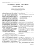
1
Track Detector Mohammad Rehawi, Rodney Brewer, Michael Reyes, Julia Williams Group 19 i Table of Contents Table of Contents ............................................................................................................... ii Schematics ......................................................................................................................... ix Figures ................................................................................................................................ x Graphs ............................................................................................................................... xi Tables ................................................................................................................................ xii Block Diagrams ................................................................................................................ xiii Equations ......................................................................................................................... xiv 1.0 Executive Summary: ................................................................................................ 1 2.0 Project Description .................................................................................................. 2 2.1 Requirements and Specification .......................................................................... 2 2.2 Block Diagrams ..................................................................................................... 4 2.3 Purpose ................................................................................................................ 7 2.4 System Theory of Operations ............................................................................... 8 2.5 Software Theory of Operation ............................................................................. 9 2.5.1 Starting Gate Assembly (SGA) ....................................................................... 9 2.5.1.1 2.5.2 Finish Gate Assembly (FGA) .......................................................................... 9 2.5.3 General Purpose Input/Output ................................................................... 10 3.0 Research ................................................................................................................ 12 3.1 Starting Gate Assembly (SGA) ............................................................................ 12 3.1.1 Theory of Operation ................................................................................... 12 3.1.2 Starting Gate Mechanism ........................................................................... 12 3.1.2.1 Magnetic Motor ................................................................................................ 12 3.1.2.2 Push/Pull Solenoids ........................................................................................... 12 3.1.2.3 Servomotors ...................................................................................................... 12 3.1.3 Pulse Width Modulation Configuration .............................................................. 9 Microcontroller ........................................................................................... 14 3.1.3.1 Atmel AT89C51 ................................................................................................. 14 3.1.3.2 Microchip PIC16F628A ..................................................................................... 14 ii 3.1.3.3 3.1.4 PWM Operations ........................................................................................ 14 3.1.4.1 Voltage Translator ............................................................................................. 15 3.1.4.2 Op-‐Amp Circuitry .............................................................................................. 15 3.1.4.3 Comparator Circuitry ........................................................................................ 15 3.1.5 3.2 Texas Instruments CC2540/AT8051 ................................................................. 14 Reference Voltage ...................................................................................... 16 Finish Gate Assembly (FGA) ............................................................................... 16 3.2.1 Poll Tree Light Assembly ............................................................................. 16 3.2.1.1 Microcontroller ................................................................................................. 16 3.2.1.2 Lighting Options ................................................................................................ 17 3.2.1.2.1 Florescent Lights ......................................................................................... 17 3.2.1.2.2 LED Lights .................................................................................................... 17 3.2.1.2.2.1 High Power LEDs .................................................................................. 18 3.2.1.2.2.2 Multi-‐Color LEDs .................................................................................. 18 3.2.1.2.2.3 Miniature LEDs ..................................................................................... 19 3.2.1.3 LED Controller ................................................................................................... 19 3.2.1.3.1 8-‐Bit Shift Register (74HC164) .................................................................... 19 3.2.1.3.2 CMOS Buffer (CD4049/CD4050) ................................................................. 20 3.2.1.3.3 LED Driver IC (TLC59281) ............................................................................ 20 3.2.2 Finish Gate Display Module ........................................................................ 20 3.2.2.1 Definition .......................................................................................................... 20 3.2.2.2 Specification ...................................................................................................... 21 3.2.2.3 Display Layout ................................................................................................... 21 3.2.2.4 Display Comparisons ......................................................................................... 22 3.2.2.4.1 Standard 7-‐Segment Display ....................................................................... 22 3.2.2.4.2 OLED Display ............................................................................................... 22 3.2.2.4.3 Liquid Crystal Display .................................................................................. 22 3.2.2.5 Processors and Drivers ...................................................................................... 23 3.2.2.6 Display Design Options ..................................................................................... 24 3.2.3 Finish Gate Detection System ..................................................................... 26 3.2.3.1 3.2.4 Finish Gate Sensor Assembly ............................................................................ 27 Finish Gate Housing Materials .................................................................... 27 iii 3.3 3.2.4.1 Wood ................................................................................................................ 27 3.4.2.2 Acrylic/Polymer ................................................................................................. 28 3.4.2.3 Aluminum ......................................................................................................... 28 Sensors ............................................................................................................... 29 3.3.1 Sensor Types ............................................................................................... 29 3.3.1.1 Hall Effect Sensor .............................................................................................. 29 3.3.1.2 IR Emitter/Detector .............................................................................................. 29 3.3.1.3 Ambient Light Sensor ............................................................................................ 30 3.3.1.4 Acceleration/Vibration Sensor .............................................................................. 30 3.3.1.5 Force Sensing Resistor (FSR) ................................................................................. 30 3.3.1.6 Capacitive Sensing ................................................................................................ 30 3.3.1.7 Sensor Pros and Cons ........................................................................................ 30 3.3.1.7.1 Hall Effect Sensor ........................................................................................ 30 3.3.1.7.2 IR Emitter/Detector .................................................................................... 31 3.3.1.7.3 Ambient Light Sensor .................................................................................. 31 3.3.1.7.4 Acceleration/Vibration Sensor .................................................................... 31 3.3.1.7.5 Force Sensing Resistor (FSR) ....................................................................... 32 3.3.1.7.6 Capacitive Sensing ...................................................................................... 32 3.3.2 Track Position Sensors System .................................................................... 32 3.3.3 Speed Detection Sensors System ................................................................ 32 3.3.4 Finish Gate Sensor System .......................................................................... 32 3.3.5 Sensor Specifications and Requirements .................................................... 33 3.3.6 Sensor Theory of Operation ........................................................................ 34 3.3.6.1 Speed Detection Sensor System ....................................................................... 34 3.3.6.2 Track Position Sensor System ........................................................................... 35 3.3.6.3 Sensor Timing ....................................................................................................... 37 3.4 3.3.6.4 Finish Gate Detection System ........................................................................... 37 3.3.7 Sensor Selection ................................................................................................ 37 Application Software .......................................................................................... 38 3.4.1 Sensor Software Overview .......................................................................... 39 3.4.1.1 3.4.2 Speed Detection Sensor Software .................................................................... 39 Main Application Software Overview ......................................................... 41 iv 3.5 Power Supply ..................................................................................................... 43 3.5.1 Preliminary Specification ............................................................................ 43 3.5.2 Input Power Considerations ....................................................................... 43 3.5.3 Power Supply Technologies ........................................................................ 44 3.5.4 Power Supply Selection .............................................................................. 45 3.5.5 Power Supply Distribution .......................................................................... 46 3.5.6 DC-‐DC Step Down Convertor ...................................................................... 48 3.6 Communications ................................................................................................ 49 3.6.1 433MHz Transceiver ................................................................................... 49 3.6.2 802.11 WiFi ................................................................................................. 49 3.6.3 RS-‐232 Standard Serial Com ....................................................................... 50 3.6.4 2.4GHz Bluetooth SoC ................................................................................. 50 3.6.5 Communication Selection ........................................................................... 50 4.0 Design ......................................................................................................................... 54 4.1 Starting Gate Design ............................................................................................... 54 4.1.1 Starting Gate Signal ......................................................................................... 54 4.1.2 Components Specifications ............................................................................. 55 4.1.3 Circuit Assembling ........................................................................................... 56 4.1.4 Mounting / Installation Hardware ................................................................... 58 4.1.5 Schematic Design ............................................................................................. 59 4.2 Finish Gate .............................................................................................................. 61 4.2.1 Finish Gate Design ........................................................................................... 61 4.2.1.1 Finish Gate Housing Design .................................................................................. 61 4.2.1.2 Finish Gate Bluetooth Chip ................................................................................... 62 4.2.1.3 Pin Assignments .................................................................................................... 63 4.2.1.4 Circuit Connections ............................................................................................... 64 4.2.1.5 Starting Signal Received/Transmitted ................................................................... 64 4.2.1.6 Final Signal Transmitted ........................................................................................ 65 4.2.2 Poll Tree Light Design ...................................................................................... 66 4.2.2.1 Components Specifications ................................................................................... 66 4.2.2.2 LED Lights Layout .................................................................................................. 67 4.2.2.3 IOUTvs VOUT, RLED, and RIREF Calculation .................................................................... 67 v 4.2.2.4 Circuit Assembling ................................................................................................ 69 4.2.2.5 Schematic Design .................................................................................................. 70 4.2.3 Display Design .................................................................................................. 71 4.2.3.1 Display Mechanism Considerations ...................................................................... 71 4.2.3.1.1 Finish Gate Display Header ............................................................................ 71 4.2.3.1.2 Audio Details .................................................................................................. 71 4.2.3.2 Finish Gate Display Assembly Detail Description .................................................. 72 4.2.3.2.1 Communication Overview ............................................................................. 72 4.2.3.2.2 SPI Interface Hardware Description ............................................................... 74 4.2.3.2.2.1 SPI Interface Detailed Description .......................................................... 76 4.2.3.3 Displays ................................................................................................................. 77 4.2.3.3.1 Place Standing Display ................................................................................... 77 4.2.3.3.2 Winning Lane's Chasing Lights ....................................................................... 78 4.2.3.3.3 Speed Displays ............................................................................................... 79 4.2.3.4 Audio ..................................................................................................................... 80 4.2.3.4.1 Starting Sound Byte ....................................................................................... 80 4.2.3.4.2 Finish Sound Byte ........................................................................................... 80 4.2.3.4.3 Audio Driver Circuitry .................................................................................... 81 4.2.3.5 Software Display Design Details ........................................................................... 81 4.2.3.5.1 Overview ........................................................................................................ 81 4.2.3.5.2 SPI Interface Software Detail ......................................................................... 81 4.2.3.5.3 MSP430 Software .......................................................................................... 82 4.2.3.5.4 CC2540 Transceiver Software ........................................................................ 82 4.2.4 Detection System ............................................................................................. 83 4.2.4.1 Finish Gate Sensor Placement/Installation ........................................................... 83 4.2.4.2 Circuit Diagram ..................................................................................................... 83 4.3 Position Sensors ...................................................................................................... 85 4.3.1 Track Position Sensor Mounting/Installation .................................................. 85 4.3.2 Track Position Sensor Placement ..................................................................... 86 4.3.3 Circuit Diagram ................................................................................................ 88 4.4 Calibration .............................................................................................................. 95 4.4.1 Circuit Diagrams for Calibration ....................................................................... 96 vi 4.5 Power Supply Design .............................................................................................. 97 4.5.1 Power Source ................................................................................................... 97 4.5.2 Regulator Circuit Design .................................................................................. 99 5.0 Prototyping .......................................................................................................... 101 5.1 Starting Gate Assembly Prototyping ................................................................ 102 5.2 Finish Gate Assembly Prototyping ................................................................... 103 5.2.1 Poll Tree Light Assembly Prototyping ....................................................... 103 5.2.2 Display Module Prototyping ..................................................................... 104 5.3 Sensor Prototyping ........................................................................................... 105 5.3.1 Track Position Sensor Prototyping ............................................................ 105 5.3.2 Calibration Sensor Prototyping ................................................................. 106 5.3.3 Finish Gate Detections Sensor Prototyping .............................................. 106 5.3.4 Speed Sensor Prototyping ........................................................................ 106 5.4 Power Supply Prototyping ............................................................................... 107 5.5 Software Debugging and Prototyping .............................................................. 108 6.0 Testing ................................................................................................................. 109 6.1 Starting Gate Assembly Testing ....................................................................... 109 6.2 Finish Gate Testing ........................................................................................... 110 6.2.1 Poll Tree Light Assembly Testing .............................................................. 110 6.2.2 Display Module Testing ............................................................................. 110 6.2.2.1 Finish Gate Display Test Procedure ................................................................. 111 6.2.2.2 Display Processor Board Operation Testing .................................................... 113 6.3 Track Position Sensor Testing .......................................................................... 114 6.4 Speed Detection Sensor Testing ...................................................................... 114 6.5 Calibration Testing ........................................................................................... 116 6.6 Power Supply Testing ....................................................................................... 117 6.6.1 Test Procedure ............................................................................................... 117 7.0 Troubleshooting ................................................................................................... 120 8.0 User Manual ........................................................................................................ 121 10.0 Administrative Content .......................................................................................... 122 10.1 Budget .......................................................................................................... 122 10.2 Milestones .................................................................................................... 125 Appendix A ..................................................................................................................... 128 vii Copyright Permissions ................................................................................................ 128 Appendix B ...................................................................................................................... 133 References .................................................................................................................. 133 Appendix C ...................................................................................................................... 135 Full Schematics ........................................................................................................... 135 viii Schematics Schematic 1 Starting Gate Circuit ..................................................................................... 60 Schematic 2 Poll Tree Light Full Schematic ....................................................................... 70 Schematic 3 Simulated Driver Circuit for Place Standing Display ..................................... 78 Schematic 4 Simulated Winning Lane’s Chasing Light Simulation Schematic .................. 79 Schematic 5 Speed Display Sensor ................................................................................... 80 Schematic 6 Finish Gate Detection System Sensor Full Schematic ................................... 84 Schematic 7 Photodiode Position Sensor Full Schematic ................................................. 89 Schematic 8 Phototransistor Position Sensor Full Schematic ........................................... 90 Schematic 9 IR – Emitter Schematic ................................................................................. 91 Schematic 10 Photodiode Circuit Diagram 1 .................................................................... 92 Schematic 11 Photodiode Circuit Diagram 2 .................................................................... 93 Schematic 12 Nonreflecting Phototransistor Circuit Diagram .......................................... 94 Schematic 13 Reflecting Phototransistor Circuit Diagram ................................................ 95 Schematic 14 Calibration Circuit Diagram ........................................................................ 97 Schematic 15 Fused Supply with Overvoltage Protection .............................................. 100 Schematic 16 Photodiode Operating Simulation ............................................................ 116 Schematic 17 Finish Gate Display Circuit Diagram ......................................................... 136 ix Figures Figure 1 Track Design .......................................................................................................... 3 Figure 2 Voltage Translation Classes ................................................................................ 15 Figure 3 Fluorescent Lights ............................................................................................... 17 Figure 4 High Power LED Lights ........................................................................................ 18 Figure 5 Multi-‐Color LEDs ................................................................................................. 18 Figure 6 Miniature LEDs .................................................................................................... 19 Figure 7 Existing Track Finish Gate ................................................................................... 21 Figure 8 Main Application Screen ..................................................................................... 42 Figure 9 Power Supply Track Illustration Distribution ...................................................... 46 Figure 10 Female DC Power Plug ...................................................................................... 47 Figure 11Male 2.1mm DC Power Plug .............................................................................. 47 Figure 12Power Transformer “A size E16” ....................................................................... 47 Figure 13 Output Pins of CC2540 Bluetooth SoC .............................................................. 52 Figure 14 CC2540 Architecture ......................................................................................... 53 Figure 15 Comparator’s MultiSim Simulation ................................................................... 57 Figure 16 Servomotors Placements .................................................................................. 58 Figure 17 Front View of the Finish Gate Housing ............................................................. 61 Figure 18 Top View of the Finish Gate Housing ................................................................ 61 Figure 19 LED Driver’s (IOUT vs VOUT) .................................................................................. 67 Figure 20 Display Processor (MSP430) ............................................................................. 75 Figure 21 SPI Master AC Characteristics ........................................................................... 76 Figure 22 SPI Connections between CC2540 and MSP430 ............................................... 77 Figure 23 SPI Interface bit Definitions .............................................................................. 81 Figure 24 Finish Gate Detection Sensor Placement .......................................................... 83 Figure 25 Track Position Sensor Placement 1 ................................................................... 85 Figure 26 Track Position Sensor Placement 2 ................................................................... 86 Figure 27 Track Position Sensor Placement 3 ................................................................... 87 Figure 28 Track Position Sensor Placement 1 ................................................................... 88 Figure 30Full Wave Rectifier ............................................................................................. 97 Figure 31 Display Connection Points .............................................................................. 111 Figure 32Display Test Connector .................................................................................... 112 Figure 33Power Supply Temperature Test Locations ..................................................... 117 x Graphs Graph 1 Speed Sensor Incident IR Drive ......................................................................... 115 xi Tables Table 1 Bluetooth USART Connections ............................................................................. 11 Table 2 MSP430 Display Pin Count ................................................................................... 23 Table 3 Material Listing .................................................................................................... 27 Table 4 Sensor Selection (Advantages/Disadvantages) .................................................... 38 Table 5 Battery Types ....................................................................................................... 44 Table 6 Voltage/Current Requirements ............................................................................ 45 Table 7 Component Power Specifications ........................................................................ 55 Table 8 Components Output Pins’ Used ........................................................................... 55 Table 9 CC2540 I/O Pins Finish Gate Assignment ............................................................. 63 Table 10 Components’ Power Specifications .................................................................... 66 Table 11 Components’ Output Pins Used ......................................................................... 66 Table 12 LED Design Layout .............................................................................................. 67 Table 13 LED Driver’s Sink Current (IOLC) vs Reference Resistance (RIREF) ......................... 68 Table 14 MSP430 SPI Pins ................................................................................................. 74 Table 15 Finish Gate Detection System Component Quantities ....................................... 84 Table 16 Track Position Sensor Component Quantities ................................................... 89 Table 17 Phototransistor Position Sensor Component Quantities ................................... 91 Table 18 Individual Subassembly Current Requirements ................................................. 99 Table 19 General Bluetooth System Pin Out .................................................................. 102 Table 20 Preliminary Prototype Checklist – To be Completed during Prototyping ........ 107 Table 21 Servomotor Test Points .................................................................................... 109 Table 22 Poll Tree Light Test Points ................................................................................ 110 Table 23 Calibration Test Points ..................................................................................... 116 Table 24 Troubleshooting Table ..................................................................................... 120 Table 25 Budget Table .................................................................................................... 123 Table 26 Sampled Parts .................................................................................................. 124 xii Block Diagrams Block Diagram 1 Controller and Interface Systems ............................................................ 4 Block Diagram 2 System Controller .................................................................................... 4 Block Diagram 3 Sensor Interface & Data Acquisition ........................................................ 5 Block Diagram 4 Display Controller .................................................................................... 5 Block Diagram 5 Start/Finish Gate Assembly ...................................................................... 6 Block Diagram 6 Detection System ..................................................................................... 6 Block Diagram 7 Bluetooth Display Interface 1 ................................................................ 25 Block Diagram 8 Display Driver Interface Method 2 ......................................................... 26 Block Diagram 9 Speed Detection System Overview ........................................................ 35 Block Diagram 10 Track Position Sensor Overview .......................................................... 36 Block Diagram 11 Speed Sensor Software Overview ........................................................ 40 Block Diagram 12 Main Power Supply Distribution .......................................................... 49 Block Diagram 13 Starting Signal Overview ...................................................................... 54 Block Diagram 14 Starting Gate Circuit ............................................................................ 58 Block Diagram 15 Finish Gate CC2540 Circuit Connections .............................................. 62 Block Diagram 16 Finish Gate Main Circuit Connections .................................................. 64 Block Diagram 17 Finish Signal ......................................................................................... 65 Block Diagram 18 Poll Tree Light Circuit ........................................................................... 69 Block Diagram 19 Finish Gate Display Communication Overview .................................... 73 xiii Equations Equation 1 Velocity Calculation ........................................................................................ 41 Equation 2 CC2540 Output Voltage .................................................................................. 56 Equation 3 Comparator’s Output Voltage ........................................................................ 56 Equation 4 RLED Calculation ............................................................................................... 68 Equation 5 RIREF Calculation .............................................................................................. 68 Equation 6 Comparator Equation ..................................................................................... 92 Equation 7 Secondary Transformer Voltage Calculation .................................................. 98 Equation 8 Secondary Transformer Current Calculation .................................................. 98 Equation 9 Reverse Rectifier Diode Voltage ..................................................................... 98 Equation 10 Full Wave Rectifier Current .......................................................................... 98 Equation 11 Servomotor Minimum Primary AC Voltage .................................................. 98 Equation 12 Servomotor Maximum Primary AC Current ................................................. 98 Equation 13 Remaining Maximum Primary AC Current ................................................... 98 Equation 14 Remaining Supply Rectifier Diode Reverse Voltage ..................................... 98 Equation 15 Servomotor Supply Full Wave Rectifier Current ........................................... 98 xiv 1.0 Executive Summary: In 1953, Cub Master Don Murphy held the first Pinewood Derby racing event for the Boy Scouts. The Cub Scouts pinewood derby popularity lead to an immediate growth in industry targeting tracks, scales, pinewood car kits, and countless other accessories. With the help of parents, Cub Scouts get the opportunity to build and customize their own pinewood derby cars. The pinewood derby inspires the youth with a sense of fair play, competitiveness, and creativity. While Don Murphy’s aspiration was to “devise a wholesome, constructive activity that would foster a closer father-son relationship and promote craftsmanship and good sportsmanship through competition” he could not have for seen its expansion and overwhelming allure in American youth today. The objective goal of this project is to integrate key features of a typical pinewood derby race that include, but are not limited to, top speed and final speed detection, track position, wireless communications, video/led display, and remote control operations. The primary motivation for this project is to design, develop, and implement a functional and deliverable track detection system. This system, known as, the Track Detection System 2013 and will be delivered to Cub Scouts Pack 497, and may be duplicated for additional Packs. This project will consist of a distributed system which will control, monitor, calibrate, and detect different aspects of a standard race. Both software and hardware will be utilized in tandem to accomplish these tasks. There are four main areas of this Distributed Control System (DCS), which include: Wireless Communication, Sensor Calibration and Verification, Display and Audio Control, and the Main Control Sequencer. A distributed system is being employed for this project because it allows each member to independently design, develop, and implement their own portion of the design. Each subsystem will have an interface protocol and be integrated into the system. The different subsystems will interact with the main controller via Bluetooth or direct inter system communications. Although this project has many challenging components its primary goal, for UCF Senior Design group members, is to hone and expand their electrical and design skills. Furthermore, this project should provide team members the opportunity to learn or experience an application based approach to engineering which will supplement traditional classroom instruction. This project should also benefit the Cub Scouts by introducing youngsters to the physical and natural sciences. 1 2.0 Project Description 2.1 Requirements and Specification The Track Detector system specifications listed in this document apply to components and subsystems unless otherwise stated. All parts of the Track Detector system has to be achieved in order to ensure a reliable and stable system. The specifications are listed below with a brief explanation. • The Track Detection System must maintain reliable communication between all components and subsystems, this specification is considered to be the most important. Collectively the group decided the best approach to this challenge would be a wireless communication protocol. Having wireless communication could eliminate the hassle of having interconnection cables between all sub assemblies. Using a wireless link would add a layer of complexity but also make the system more versatile while providing a neat interconnection between components. In addition group member would benefit from using a new industry standard technology as well as programming a transmitter and the receiver protocol. • The Track Detector system must be electronically controlled and automated. A main controller will be used to initiate and monitor all aspects of the system while in use. Communication with all sub systems and assemblies will be done using Bluetooth, which is a great way implement the wireless link between sub systems. Having a main controller in the system simplifies mass communication between multiple endpoints. The system, for example, should start a race by lowering the starting gate electronically and resetting it automatically, without any human intervention. • Speed Sensors and Track Position sensors should perform all speed and position calculations, if required, and any calibration functions required. Sensors accuracy and requirements are specified in later sections of this document. • The Display Module is a great way to add visual effects to the project. The results of the race will be displayed on a series of seven segment led elements. The data displayed for each lane with a time, speed, and a position. There are more options that can be added to the Track Detector’s Finish Gate Display such as audio or even graphics. • Power requirements for this system will be distributed from a single supply. The power supply will have an input of 120VAC 60Hz and produce all output voltages required. Having non-isolated power supplies can cause interference and may damage other sensitive components of the Track Detector systems. The main power requirements will be 2 servo 5V 2A supplies, a shared 5V 1A supply and a 12V supply. Any additional supply loads will cause a change in the power supply requirements and therefore we will need to maintain strict compliance to loading and current consumption. 2 • Since the sponsor is going to support only a little amount of money, cost can be an issue. Group members have to search for the most reliable, least cost components. Sampling parts can be a great way to decrease the cost. Most companies have sampling for new parts available in the market. Texas Instruments, Newark, Microchip, and Fairchild are some companies who have a wide variation of sampling parts. Some companies, such as Microchip, have limitations on sampling. While on the other hand, Texas Instruments allows sampling for 5 items at a time, as many times needed. So group members have to make sure on the most expensive parts to be sampled first. In addition, development kits have to be taken into consideration. Parts sampled or bought must fit and be programmed using the development kit’s available for the group. • One of the most important specifications is safety, since the final product will be delivered to the Boys Scouts of America, Pack 497 it is required for the Track Detector system to be safe. The Track Detection system will be used in the proximity of many children. Children are by nature, nosy and want to play around with stuff, if the Track Detector isn’t safe to be around children, there is a possibility of injury or electrocution. A preliminary design for the Track Detector has been conceptually design to show how and where each part should be placed on the actual track. This design is shown in the figure below. Items placed on this layout are for reference only. U SIDE VIEW (Single Lane) Final Speed Sensor C F Start Gate Assembly Max Sped Sensor (x2) Track Position Sensors (x4) Finish Gate Assembly Computer / Laptop Finish Gate Assembly Track Position Sensors (x4) Final Speed Sensor Max Sped Sensor TOP VIEW (Single Lane) Figure 1 Track Design Start Gate Assembly 3 2.2 Block Diagrams Block Diagram 1 Controller and Interface Systems Block Diagram 2 System Controller 4 Block Diagram 3 Sensor Interface & Data Acquisition Block Diagram 4 Display Controller 5 Block Diagram 5 Start/Finish Gate Assembly Block Diagram 6 Detection System 6 2.3 Purpose This is a humanitarian purpose project for the Boys Scout Pinewood Car Race. The Track Detector System should simplify the work done for the car race done yearly in the Boys Scout. Having one controller controlling every part on the track should simplify and have the track platform clear from cables and moving people to achieve specific actions, such as the starting gate latch movement. The results from each part of the track detector are going to be sent to the main controller; in addition some information such as max and final velocity, rank, and time is going to be shown on the display screen above the finish line. Calculating, analyzing, and sending data to the main controller simplifies and makes it faster to compute the data required for the race and makes it more reliable to see who won the race. Computing and showing data to children is important to show how physics works in real life. Also having the detection system on the finish gate, the detection system makes it more reliable on who won the race. If the signal on one of the lanes gets interrupted, the main controller would know which lane has been interrupted and the data will be sent to the controller. This detection system simplifies the work that needs to be done by a physical person watching who won the race. For example, if two cars have almost the same speed and pass the finish gate with less than 1 second difference. The detection system should detect the difference, but a person might not. This makes the track detector more reliable on getting the data needed for the race. The Track Detector should make children participating and watching the race interested in physics. It would also show how physics is being applied in real life by showing max and final speed and time on the display. Showing the max velocity, children would learn that the max velocity of the car is when it starts at the end of the inclined portion of the track, right after the potential energy is converted to kinetic energy. Also showing the final velocity, children would notice and learn that the velocity decreases as the car moves along the track with no power being supplied to the car. Time, the difference between the initial – final velocity over distance traveled, shows that the higher the max velocity, the faster in time the car would travel over the track. This is a great way for learning especially for visual learners who need to see how things are applied. The Track Detector is also a great way on dealing with more than one type of electrical component. It would include learning on how to deal with sensors, using PWM pulse, power supply management, and more electrical components. The Track Detector is a great senior design project because it is fun to do and have a lot of features to deal with. 7 2.4 System Theory of Operations The Boy Scouts of America Track Detection System is a distributed system of sensing, control, and display. Each subsystem is considered a client, and while its operation is controlled from the host controller they act as an autonomous system entity. The host controller, herein called the master controller, will orchestrate the overall progression and sequencing of a race or user initiated actions such as calibration. The Track Detection System (TDS) is comprised of five sub-components; the Master Controller (MC), the Speed Detection Sensor system (SDS), the Track Position Sensors system (TPS), the Starting Gate Assembly (SGA), and the Finish Gate Assembly (FGA).To begin the master controller will acquire all subsystem handles and configure the messaging communication protocol. After the brief startup routine the master controller will indicate to the user that the TDS is ready to race. The user will initiate a race by commanding the master controller to transmit the “BEGIN_RACE” command over the wireless messaging link. The FGA, which contains the starting sequencer and display, will receive, decode and process this command. The FGA will clear all display elements, begin the tree light sequencer, and then send a “START_RACE” reply to the master controller. The master controller then instructs the SGA to activate the servo latched starting gates in turn releasing the racers down the inclined portion of the track. After a brief delay, approximately 5 seconds, the SGA will automatically reset its servo latch to its initial starting position. As the racecars velocities increase they reach a maximum speed at the base junction where a SDS is located. Crossing the SDS plain the maximum instantaneous velocity of each racer is accurately calculated and then transmitted to the master controller for displaying on the FGA.As the racers continue to zip down the track each will obstruct one of the four TPS systems. Each TPS system will transmit its location back to the master controller using the command structure “TPSXY” where X is the lane number and Y is the TPS sensor number (1 thru 4). As each racer reaches the finish line, they will cross the final SDS sensor. The minimum instantaneous velocity of each car is accurately calculated and transmitted the master controller. After calculating the average speed the master controller will save them to memory for later transmission to the FGA. Immediately after crossing the finish line the FGA will detect and display lane position as well as the calculated speeds transmitted from the master controller. The FGA display controller will continue to display lane position, average speed, total time, and toggle between min and max speeds until the “BEGIN_RACE” command is received from the master controller. The “BEGIN_RACE” command will automatically reset the FGA displays and setup the system for the next race. 8 2.5 Software Theory of Operation The following sections will discuss the software used to control, communicate and monitor the Track Detection System. Each section will include a software block diagram that will be used to break down the steps required to interface each of the components. As a distributed system, it is imperative, that no communication, operation, or function of peripheral devices compromise the main controllers’ processor. For this reason all external devices of the system will control, detect, and communicate on an individual basis. During any peripheral device power up routine there will be a minimum 30 second delay after configuring the Bluetooth controller. This delay is required to ensure that the peripheral device is ready to begin communications with the host controller. 2.5.1 Starting Gate Assembly (SGA) The Starting Gate Assembly contains a Bluetooth controller used to drive the servo actuator motors which are directly connected to the starting gate mechanism. A PWM signal, generated by the Bluetooth controller, is passed through a level translator or shifter in order interface it with the starting gate mechanism servo actuator motors. At system power up the Starting Gate Assembly will begin its configuration process. This process will setup the Pulse Width Modulation (PWM) standard, which is required to control the start gate mechanisms. Directly following the PWM setup procedure a minimum 30 second delay will begin. Immediately following the pre-programmed delay, the Starting Gate Assembly will initiate the Bluetooth pairing request with the host controller. Since the Starting Gate Assembly is activated only upon receiving a “START_RACE” command it will be placed in a holding state after power up. When receiving the “START_RACE” command trigger, the Starting Gate Assembly will promptly perform the start procedure operations and then actuate the start gate mechanism 90º in less than 100ms. After actuation, a pre-programmed delay of 5 seconds will begin, this delay guarantees that no interference between the gate assembly and the racers will occur. The final Starting Gate Assembly operation will be a reset operation, which will return the start gate mechanism to 0º in approximately 2 seconds. 2.5.1.1 Pulse Width Modulation Configuration The steps to follow will define the PWM configuration process used by the Starting Gate Assembly. Setting bothP1DIRand P1SELregisters to 0x02 will configure Port 1; Bit 2 as the starting gates PWM output pin. This output from the CC2540 2ill drive a level converter which is subsequently connected to the gate mechanism servo motor. Assigning the proper PWM duty cycle and period to T1CC0L and T1CC0H to the desired value will effectively drive the servo motor to either 0º or 90º depending on the required demand. Writing any non-zero value to the T1CTL register will start the PWM output. 2.5.2 Finish Gate Assembly (FGA) The Finish Gate Assembly contains the finish line detection system as well and logic as well as the display controller. The Finish Gate Assembly utilizes the CC2540 Bluetooth SoC and is configured as a general purpose interface device. The display control module is interfaced with the assemblies Bluetooth controller via a SPI/I2C bus. When directed by the main controller, the finish gate Bluetooth controller will initiate communications with the display control module to display race parameters and data. Race parameter data includes, but is not limited to, race position (1st through 4th), minimum and maximum 9 speeds, as well as average speed. Indicators associated with lanes, tracks, or an individual race will also be controlled by the display controller. At system power up the Finish Gate Assembly will begin its configuration process. This process will configure the General Purpose I/O ports used for the detection of lane triggering as well as the required interrupts. Directly following the GPIO and Interrupt setup procedure, a minimum 30 second delay will begin. Immediately following the pre-programmed delay, the Finish Gate Assembly will initiate the Bluetooth pairing request with the host controller. Since the Finish Gate Assembly is activated only upon receiving a detection interrupt signal or a command from the master controller it will be placed in a holding state after power up. The Finish Gate Assembly has an interrupt routine used to determine track status. When an interrupt is triggered, or invoked, the software will advance to the next state depending on the current state of the machine and the interrupt received. This state transfer process must be extremely fast and not allow a stalled state to occur, for any reason, as this could inadvertently cause false or missed detections. After the detection trigger is received, the controller will determine all appropriate race parameters, such as position, time, and lane. The controller will then transfer the appropriate information to the Display Controller, increment to the position counter, and then either enter a hold to reset state or hold for trigger state. The hold for reset state can be cleared either by receiving the “CLEAR” command or the “BEGIN_RACE” command initiated by the main controller. The “CLEAR” command will only reset the Final Gate Assembly to a pre-race state and not actually start another race. 2.5.3 General Purpose Input/Output The CC2540 Bluetooth chip has 21 digital I/O pins that are shared between multiple functions such as ADC, PWM, Capture/Compare, and other useful functions. For this reason each pin of the CC2540 must be programmed and configured to support the required functions. The Finish Gate Assembly will use the SPI/I2C bus to communicate with the LED Pole Light driver chip as well as the Display Control Module. There are two USARTS (Universal Serial Asynchronous Receiver/Transmitters) that must be configured for this particular purpose. Table 1below describes the physical ports, pins, and configuration options required to utilize the USARTS for our application. To make use of USART0 or USART1 the appropriate Peripheral Control Registers (PERCFG) must be configured so that both USARTS can be implemented for simultaneous use. USART0 will interface with the Display Control Module, using configuration A0, while the LED Pole Light driver chip will be connected to USART1, using configuration B1. This will allow us to connect and communicate with multiple devices using the same Bluetooth controller located in the Finish Gate Assembly. The port direction registers associated with each USART will also be configured as required to functions as designed by the SPI/I2C protocol. For instance, if configuration A0 is used, then Port 0 Pin 3, MOSI will be configured as an output. The associated Precedence Register (P2DIR.PRIP0) and Selection Register (P2SEL) will also be configured at this time so that the USARTS have the highest precedence and are enabled. 10 Configuration Device A0 USART0 A1 USART0 Alternate 2 B0 USART1 B1 USART1 Alternate 2 Name C SS MO MI C SS MO MI C SS MO MI C SS MOSI MISO Port Pin 0 1 0 1 Table 1 Bluetooth USART Connections 11 5 4 3 2 3 2 5 4 5 4 3 2 5 4 6 7 Description Serial Clock Slave Select Master Out (Slave In) Master In (Slave Out) Serial Clock Slave Select Master Out (Slave In) Master In (Slave Out) Serial Clock Slave Select Master Out (Slave In) Master In (Slave Out) Serial Clock Slave Select Master Out (Slave In) Master In (Slave Out) 3.0 Research 3.1 Starting Gate Assembly (SGA) 3.1.1 Theory of Operation The theory of the starting gate is having a starting mechanism that would move the latch electrically. The starting gate is supposed to get a signal from the poll tree light after the light’s sequence has been performed. The signal should start the mechanism of the starting gate. The motors attached to the latches should be supplied with enough torque and power to lower the latch within no time. All lanes should be lowered at the same time so no discrepancy occurs. Since there are 2 separate tracks, the two servos are going to be connected using one circuit. After the latches are lowered and cars go on the track, the motors should return the latches to its initial position. 3.1.2 Starting Gate Mechanism The specifications of the moving mechanism for the starting gate opening are a low voltage power requirement, fast moving mechanism, and a small sized circuit. There are several mechanisms of building the circuits according to the requirements given. 3.1.2.1 Magnetic Motor The first approach is the magnetic motor. The magnetic motor gate requires a flux coil in order to move the latch. The magnetic gate doesn’t need power requirement or power source; it will depend on earth’s gravity and magnetic field theory for it to turn the latch. The speed for turning the latch is going to be a little bit slower than the required speed. Having the speed of the latch slower than expected can have cars get stuck on the rod coming out of the latch or have opening discrepancies between the tracks. In addition, a person should trigger the magnetic flux in the motor for it to start. Without the magnetic flux triggered, the magnetic motor will not start. Usually a magnet is moved in a specific direction to trigger the magnetic flux. 3.1.2.2 Push/Pull Solenoids A second option that can be considered is a solenoid. Solenoids use a magnetic field coil in the middle to push or pull on something. Solenoids are a great way to deal on moving parts. These parts use the same concept of the magnetic motor but having the electric voltage deal with the moving mechanism. Solenoids are one of the cheapest components that can be found to move the latch. The range of the solenoids power requirement is really high; most solenoids require 12 – 24 V. This requirement for the solenoids doesn’t match the requirement for the Track Detector. It can be a backup plan if the third option doesn’t work properly. 3.1.2.3 Servomotors The servomotor is another approach for the moving mechanism. This approach is better because it requires less power. The range power requirement for servos is from 4 V to 7 V depending on how fast it should be, the weight of the attached object, and the time it 12 takes to turn. Most servos usually turn a 60-degree turn in 0.15 seconds. Having the servomotor turning the latch in 60 degrees within 0.15 seconds is going to have latch lowered at a high speed, which should eliminate any discrepancies between the starting for all the cars. The size of the servomotor is smaller than the magnetic motor gate. In addition to the specifications given for the servomotor, the price of the servomotor is cheaper than the magnetic motor. For the servomotor, a signal from the main controller triggers a PWM signal using the microprocessor used in the starting gate to make the servomotor lower latch and reset it. Most servomotors have almost the same specifications. The difference between most servos is a +/- 0.03 seconds per 60 degree turn when operating either at 4.8 V or 6V depending on the manufacturer. Since the two tracks are going to be side by side, two servos are required to operate a 4-lane race, one on each track. Servomotors prices range from $15 up to $200. For the track detector, a regular, reliable, properly functioning servo is required. If all requirements listed are in all servos, the price of the servos is the only thing that differs. Most companies make two types of servomotors, analog “standard” servos and digital servos. Both servos are made from the same material; the only difference between the two types is the way that the servos work and needs to be programmed. In analog servos, the pulse is generated at high torque for a short period of time, such as 50 µs. While the digital servos, which are a better servo use for the gate, use a constant torque controlled by the microcontroller at a longer period of time, such as 300 µs. The digital servos are better because they give constant torque generated and controlled by the microcontroller. Hi-Tec, JR, and Futaba are three companies known for manufacturing servos for RC games. Since most servos manufactured have the same specification by a +/- 0.03 s for a 60-degree turn, the search has been narrowed on which company makes cheaper reliable servos for the use for the starting gate. Two servos are needed which means the cost of the servo is going to be doubled. JR and Futaba manufacture more expensive servos than Hi-Tec. Futaba manufacture servos at higher cost, but the spare parts for the servos are cheaper than any other company. Hi-Tec on the other hand, manufactures cheaper servos, but the price for the spare parts is higher than that of Futaba’s spare parts. HiTec servos are cheaper by about 80% or more than Futaba’s. This eliminates the option of having a Futaba servo. The Hi-Tec manufactures the HS-5055MG, are good, reliable, and inexpensive servos for the use of the starting gate. The voltage requirement for the servo is 4.8 V to make a turn of 60-degrees in 0.17s and a 6 V to make a turn of 60-degress in 0.14s with no load attached. The max current required to have the servo supply a max torque is 2 A. The pulse from the microcontroller should be between 4.8V and 6V. 13 3.1.3 Microcontroller Having the DC motor known, the microcontroller search has been narrowed. The Servomotor requires a microcontroller that has a pulse-width modulation signal that would make the servo turn. In addition, the number of bits doesn’t need to be more than 8 bits. There is more than one company that builds a PWM microcontroller. Some of those companies are Atmel, Texas Instruments, Microchip, and others. 3.1.3.1 Atmel AT89C51 Atmel has a microcontroller “AT89C51” which is also known as 8051 microcontroller. This microcontrollercan generate a PWM signal and it’s an 8-bit microcontroller. The chip has been tested on a servo, and it made the servo move clockwise and counterclockwise by programming it. It was also used to make the user input the degree desired to turn the servo. This AT89C51 microcontroller is a really good controller, but the problem is it is a 40-pin microcontroller. The only use for this microcontroller in this circuit’s purpose is to generate a PWM signal. This would be a waste of space and the circuit would be bigger than required. So a smaller microcontroller might be a better choice for mounting it on the PCB board since the only function of the microcontroller is the signal to turn the servo on. 3.1.3.2 Microchip PIC16F628A Another microcontroller from Microchip is “PIC16F628A” has been found. This microcontroller has the requirements needed for turn the servo clockwise and counterclockwise, but as the Atmel microcontroller, the pin-size of the microcontroller is still big regarding the use of it. This chip is a 24-pin chip. Texas Instruments has a wide variety of high performance low voltage microcontrollers. The class C2000 had a microcontroller that sends a PWM signal. 3.1.3.3 Texas Instruments CC2540/AT8051 While searching for a microcontroller, another search was being conducted for a Bluetooth communication chip. The CC2540 Bluetooth chip made by Texas Instruments includes an 8051 microcontroller. This 8051 microcontroller contains 4 timers, 2 of which support sending a PWM signal through one of its digital I/O pins. In addition that it functions as both the communication for that part of the system and a microcontroller for the servo, the size of the chip is tiny that would decrease the size of the PCB board used for the starting gate. Also this chip requires less power than the other chips found. The power consumption of the Bluetooth system on a chip ranges from 2.0 V to 3.6 V. 3.1.4 PWM Operations The PWM pulse generated by the Bluetooth microchip holding data on depends on the input voltage for the Bluetooth chip. The Vmax output of the I/O pins is Vo = VDD- 0.3 V. In this case if VDD is at the max (3.6V), the max output pulse voltage will be 3.3 V. There 14 are a couple of ways to increase the pulse voltage. The easiest ways are using a chip that would increase it. 3.1.4.1 Voltage Translator An easy approach is having a single component named as Voltage Translators to translate the output pulse of the microprocessor to the needed output voltage. Fairchild is the most known company that manufactures this type of semiconductors. Unlike other components or ways to deal with the increase of the PWM signal, once these components are built for the required output signal, they cannot be changed. The list of voltage translators is shown in the figure below. If used, the green fixed voltage translators are the one to be picked from this list. Figure 2 Voltage Translation Classes 3.1.4.2 Op-‐Amp Circuitry Another approach is having an op-amp. LM324 is an op-amp that can increase the voltage with a positive gain if used as a non-inverting amp. The required input pulse voltage according to the datasheet of the servomotor is from 4.8 V to 6 V. In order to get a gain the input supply voltage for the op-amp should be 9V or more. If less than 9V will be supplied to the op-amp, the input pulse will decrease instead of increasing. This could be an issue because the starting gate will be only supplied with a 5 V. 3.1.4.3 Comparator Circuitry A third option is having the LM339. The LM339 is a comparator that can have a supplied voltage of 5 V and increase the input pulse. The LM339 requires a reference voltage that will increase the input pulse by that amount of the reference voltage. Having a simple component that increases the pulse with the required supplied DC voltage is the best way to approach this problem. Including this comparator in the circuit to increase the output voltage will be easily adjusted by changing the reference voltage needed. For example, if 15 the output voltage is less than the one needed, then a different reference voltage will be implemented; which is different than the voltage translator that would require changes to the minor component values to get the required output voltage. 3.1.5 Reference Voltage Having the comparator needed in the circuit, a reference voltage has to be applied to the component. The reference voltage can range from 1.5 V to 2.0 V depending on the output voltage of the Bluetooth chip pin. To be on the safe side, a 2.0 V is the best to have to eliminate any miscalculations of the actual values. The reference voltage has to be a static input voltage, which means that having a power supply supplying a reference voltage is a bad idea. Using the Webench Design Center that Texas Instruments to pick a specific component that has a supplied voltage of 5 V and an output reference voltage of ~ 2.0 V is an easy way to search for the component. The Webench website gave results for REF 29XX class. The best to be used in the starting gate are REF2920 and REF2930. Both components have the same specifications. Each component would supply and output reference voltage of 2.048 V when supplied with 5 V input. The accuracy of the output voltage is 2% that eliminates any wide range fluctuation of the reference voltage. 3.2 Finish Gate Assembly (FGA) 3.2.1 Poll Tree Light Assembly 3.2.1.1 Microcontroller The finish gate will include a Bluetooth chip (CC2540) for communication with the main controller. As the previous research for the starting gate microcontroller has been conducted, the Bluetooth chip includes an 8051 microcontroller with 21 I/O programmable pins. This simplified the research for the LED microcontroller by using an already used chip on the finish gate board. 16 3.2.1.2 Lighting Options 3.2.1.2.1 Florescent Lights Fluorescent lights are the conversion of UV light into visible light. This is caused when electrons flow through the fluorescent tube colliding with mercury making photons release UV light. The glass tube of the fluorescent light is covered with phosphor coating on the inside, which converts UV lights into visible light. This makes the requirements of fluorescent lights difficult to include in the finish gate. Fluorescent lights require highvoltage to start, and a high frequency AC current while it’s on. Figure 3 Fluorescent Lights 3.2.1.2.2 LED Lights LED lights on the other hand work using a p-n junction photo diode. LED lights work when electrons jump between junctions then recombining with atoms. When combined together, photons are released. This would result in the light generated in LED lights. LED lights are different that fluorescent light; first, LED lights do not to be ignited in order for them to start such as the fluorescent lights. Secondly, LED lights require less voltage power and current through each diode. The running control for LED lights is constant current while for fluorescent is high frequency AC current. 17 3.2.1.2.2.1 High Power LEDs There are many types of LED lights that can be used in the track detector. High power LED lights have a stronger light output than any other LED light manufactured. Those LED lights have a longer life span than other LED types. There are a couple of disadvantages for those type of LED lights. One of these disadvantages is overheating. Since they overheat, they need to be mounted on a heat absorbent material. Another disadvantage is the cost of each diode is higher than the rest of the types. Figure 4 High Power LED Lights 3.2.1.2.2.2 Multi-‐Color LEDs Another two common types are the Bi-color and Tri-color LED lights. Those photodiode components emit two or three colors instead of one. This is because the bi-color LED lights are connected to one lead and the tri color LED lights are connected to two leads. Each light can light up simultaneously and is controlled using the microcontroller. The use of this type of LEDs is not necessary for the track detector since only one color is needed to light up at once. Figure 5 Multi-Color LEDs 18 3.2.1.2.2.3 Miniature LEDs Another type that is best fit for the use in the poll tree light is the miniature single color LED light. This type requires a low constant current to light, normally around 10 mA and the max that those LED lights that can take is 20 mA. The forward voltage range for those LEDs differs by the manufacturer and the color output. In average the range of the lower voltage to the upper voltage is +/- 0.2 V depending on the color and manufacturer, such as the green LED light required a forward voltage from 3.2 V to 3.4 V. In addition, they are designed to surface mount and have a through hole design which makes it easy to mount. Figure 6 Miniature LEDs 3.2.1.3 LED Controller To be able to control several LED lights at once without using more than couple of pins from the Bluetooth chip, an LED controller is needed. The average input current to light up an LED light is around 10 mA, and the max current that most LEDs can take is about 24 mA. There are a couple of ways to approach the controller such as using shifters, buffers, and LED drivers. 3.2.1.3.1 8-‐Bit Shift Register (74HC164) The 74HC164 shifter is an 8-bit shifter that can be used to control LED lights. The shifter requires 3 pins from the Bluetooth chip. The shifter functions at an input voltage between -0.5 and +7 with an output current for each pin of 20 mA. The shifter will start at pin 0 and ending at the user input pin number by incrementing the number of pins. This would result in turning on the LEDs on only one output pin at a time. Using this shifter or LED controller can have a limitation in the sequence of how the LED lights are wanted to be on. 19 3.2.1.3.2 CMOS Buffer (CD4049/CD4050) The second option for controllers a CMOS buffer, the CD4049. This buffer is usually called the line drive, which requires a voltage input range from 5 V to 15 V depending on the output’s requirement. The line drive takes in the data from the Bluetooth chip using one pin and manages the turning on of the LED lights, such as the shifter above. The buffer is only limited when it comes to sequences of lightning the LEDs. The CD4049 gives more output power and can control the sequence of LED light in more options unlike the 74HC164. 3.2.1.3.3 LED Driver IC (TLC59281) A third chip has been found that can control the LED lightening in any sequence required by clocking the required pin to turn on. The TLC59281 is a 16-bit constant current LED driver made by Texas Instruments. The power requirement for the TLC59281 is 5 V. The output current is 40 mA for each pin, which is more than enough to turn on the LED lights. The TLC59281 LED driver is the best component found to control the poll tree light lightning system for any sequence given. 3.2.2 Finish Gate Display Module 3.2.2.1 Definition This section defines the research that is involved in the display unit assembly board that will be located within the finish gate unit. As the research is progresses and becomes completed, the definition may change slightly. The final design and specifications will be in the Hardware Detail Design section of this document. The display assembly operation will accept data from a SPI bus on the Bluetooth chip. The display will have its own dedicated processor. This processor will drive the place standings, (4 large LEDs, one per lane) and smaller LEDs for speed data (4 displays per lane totaling 16 LEDs). This processor will also light the sides of the winner’s lane with flashing (chase style) single LEDs. If it is possible, this processor will also be the storage place for the sound bites to indicate the beginning and the end of the race. The audio driver circuitry will also be contained on this pc board if this research deems it to be possible. The display will also have the starting tree lights in the middle of the tracks (two on each side). The Bluetooth data inputs for the finish gate will be: • A ‘start of race’ signal for the starting tree lights and possible sound bites will come from the main controller. • The speed data from the sensor Bluetooth chip. • The place standings for each lane, this data is supplied locally to the finish gate transceiver for wireless transmission and through the device to the displays. 20 The Outputs used by the finish gate include: • Place standing displays (4) output from a local processor. • Speed displays (4 per lane totaling 16) also from the local processor. • Chasing LEDs (8) for the winning lane output from the processor. • Starting gate tree lights. This information will come directly from the Bluetooth. 3.2.2.2 Specification • The display should be visible up to 50 feet • Display Dimensions: o Shall be centered over each lane of each track o Outside dimensions are 3.5 inches per slot times 4 slots, add 1/8 inch for connections (14.375 inches) • The Display should have a minimum number of inputs per digit to realize a minimum I/O for a more economical processor. • Compact design, should fit within the Finish Gate Assembly • It should be a low cost device 3.2.2.3 Display Layout A similar design can be found at: http://www.besttrack.com/champ_timer.htm and is displayed in the figure below. Figure 7 Existing Track Finish Gate This gate’s display and design is looks great, however, the scouts that we are building the product for assemble their racetrack on the floor; therefore it would be more useful to mount the display either at an angle or on the top of the gate. 21 3.2.2.4 Display Comparisons 3.2.2.4.1 Standard 7-‐Segment Display The first, most obvious choice for a display would be the 7-segment display LED. These come in a variety of colors and sizes. The 1.5 inch Newark P/N 26M2805 green component is visible much further than 50 feet. The 0.4 inch (10mm), Newark P/N 19J8004 would be used for They are also low cost and readily available. The disadvantage is that we will need at least 7 I/O pins per digit, or 4 with a logic gate design. This will either take up a lot of I/O on our processor, or a lot of real estate on the board. Due to the cost and availability alone, we will choose this if we don’t find anything comparable to it. 3.2.2.4.2 OLED Display When evaluating OLED displays, the versatility they have is attractive. That is, any alpha, numeric, or graphic theme can be displayed. The low power consumption and the unlimited viewing angle are more great points that are hard to ignore. Another positive for this is the input is serial, avoiding having to use excessive output pins from a controller. It may even eliminate the need for a processor at all, since the information from the main controller and the sensor sub-system will already be processed and the need for a local processor was highly due to the output pin limitations of the wireless chip. An OLED would wire almost directly from the Bluetooth to give a display. The negative points regarding the OLED are the pricing and the size limitations. A modestly priced device is about thirty five dollars. This is way above budget since the devices size would force the purchase of 4 of them one device per lane (2 tracks), and another for each side. This prospect was quickly eliminated, but it was exciting to consider its implementation. 3.2.2.4.3 Liquid Crystal Display The LCD considered were questionable as to whether they would be viewable from a distance without a backlight applied. The 7 segment displays had the same input pin requirement, therefore no gain here. The price was comparable to the LED display but without the luminosity that the project requires. This option was quickly disregarded. 22 3.2.2.5 Processors and Drivers Since the Bluetooth transceiver does now have the I/O, specifically the output capacity needed for the displays we required for this project, it was decided to add a processor to the finish gate board. The output we need is the following: Description Place standings (4 outputs times 1 per lane, time 4 lanes) also needs to drive 2 LEDs (front and back) Speed display (4 digits per lane times 4 output pins times 4 lanes) also needs to drive 2 LEDs (front and back) Winning chase lights 1 per lane (may not be needed, looking into using existing circuitry) If not possible, we may need this. Sound output? (optional) Poll tree lights at finish gate (will be using Bluetooth output) total Number of output pins 16 64 4 1 N/A 80-85 pins. Table 2 MSP430 Display Pin Count The criteria that we are evaluating all the display assembly processors are: 1. Can it easily interface with Bluetooth device? 2. Do we have a good support source? 3. Does it provide 80 inputs (minimum)? 4. Can one output drive two LED display circuits? 5. Is the cost of the development board and processor reasonable? 6. Is it possible to use it for the audio sound bites (optional, it may be done with Bluetooth)? Each of these questions along with additional comments on the processors will be addressed in the paragraphs below. The main processor under consideration is the MSP430. At this time there are two other considerations to be investigated, the PIC and an FPGA. Texas Instruments MSP 430 has been inquired about, since the college has development boards readily available and they are inexpensive (question 2 and 5). Also, other students have used it and it has been evaluated in house by UCF support personnel. There are currently eight products with 87 I/O pins. All of these have the embedded SPI bus interface and have the option of either an internal or external clock, for timing to the transceiver. They are all the same physical package and have the same core size and RAM. The difference between them is the supply power and the RAM and the program memory size. Since we do not expect to do much of the processing within the chip, the specific part number of interest is the MSP430F5419IPZ – IC since it is the least expensive at $6.82 apiece. This chip is also readily available for purchase. 23 Another consideration is the PIC processor. The processor that is under consideration is the PIC24HJ128GP210-I/PF, cost is 6.19 apiece and is also ready to ship. It is also has an inexpensive start-up cost, with a starter kit possessing everything you need to program, debug and explore the device costs $60.00. This also interfaces via SPI and has the same core, program memory, and package dimensions as the MSP 430 chip. Here, it should be noted that the on-line support and videos seem to show the PIC to be easier to use and has more discussion boards devoted to it. The last option views a different approach to solving the real estate problem discussed in the specifications part of this section. Why not integrate our driver circuitry within an FPGA? This would certainly simplify the board layout process and wrap our cost into virtually one chip. The possibility was worth investigating. The FPGA and Xilinx tools are readily available since the university uses it for the 3342 lab. All the group members are also experienced with it since we all completed this lab. Furthermore, these chips and the Xilinx tool with the HDL input such as VERILOG and VHDL are used heavily in local industries, Lockheed-Martin, Harris and Collins just to name a few. The added benefit of more experience with Xilinx and FPGAs could only be good for the group. With this approach, we will need 144 pins, due to the drivers being internal. The Altera part number of the chip under scrutiny is EP4CE10E22C8N, the cost is $22.45 and is readily available. Given the performance of an FPGA and the versatility, cost and complexity, this choice may be overkill, but with the independent experience gained, it may be worth it. In conclusion, the best choice for this project is the MSP430 due to development tool access and the availability of support. Texas Instruments has a rep in the building about twice a month. 3.2.2.6 Display Design Options There were two main electrical approaches considered to send the place and speed information from the processor to the display itself, the direct method or communication through a port expander to a driver circuit. With the direct method, the processor would send out for each seven segment display, four discrete BCD valued outputs and these would be sent to a driver and finally to the display itself. This is very simple and direct. Just one of the 4 redundant circuits is shown below explaining this method. It would be easy to design, troubleshoot, and it would be serviceable if repairs were needed. The only real disadvantage is that it would require a lot more outputs from the processor chip. Assuming both a front and rear display driver having a parallel connection from the processor output, it would take at least 80 output pins from a processor. This is not including the audio expansion option that was outlined. Also, the winner’s chasing light display will be a parallel connection to the 4 input logic NOR gate that is set if the BCD input is a one. Another disadvantage of selecting a high output port processor is that the processor’s capability would be underutilized, since little actual processing would need to be done at this point since each it was determined that each assembly would send out its 24 own final data in a readable form. These disadvantages are not significant, since processors, especially the MSP430 are inexpensive. This design, surprisingly would take up much less real estate on the board also, with many less solder connections to fail. Finish Gate Bluetooth Chip MSP430 Processor SPI Interface X4 X4 BCD-‐7segment decoder circuit BCD-‐7segment decoder circuit Win-‐place-‐show display Speed 7-‐segment display If 0001 then enable Winning lane chasing LED lights Block Diagram 7 Bluetooth Display Interface 1 On the other hand, the method of using a port expander would eliminate the need for so many outputs from the processor chip, or even to have a processor chip at all. Checking into the possibility of this information being sent directly from the Bluetooth chip to eliminate the need for the MSP430 would be the ultimate goal, if this can be done, the expander method should be selected. 25 A SPI bus, for example, would be used by the output port of the transceiver and sent to general purpose parallel I/O expansion device, such as the microchip MCP23S17. This is a 16 bit device that could be used for all four of the speed displays, for example. Another one could be used for the place standings in a configuration as shown in the block diagram below. SPI Interface X8 MCP23S17 Port expander BCD-‐7segment decoder circuit Finish Gate Bluetooth Chip SPI Interface X2 If 0001 then enable Winning lane chasing LED lights MCP23S17 Port expander Speed 7-‐ segment display BCD-‐7segment decoder circuit place 7-‐segment display Block Diagram 8 Display Driver Interface Method 2 3.2.3 Finish Gate Detection System The Finish Gate Detection System will determine, with a high degree of accuracy the order in which racers cross the finish plane. The system will use a non interference based method of detecting race cars as they finish the race. The sensors being used need to be very precise so that the correct order is recorded. In addition, the sensors need to cover the entire width of the lane. The reason for this is so that if any part of the car crosses the finish line, the finish gate sensors need to detect the car. The information detected by the finish gate sensors will be eventually sent to the display and the computer so that the outcome of the race will be displayed. 26 3.2.3.1 Finish Gate Sensor Assembly The finish gate sensors require a combination of the features found in the speed position sensors and the track position sensors. These sensors are responsible for the outcome of the race so precision and accuracy is of outmost importance. To achieve the accuracy and precision necessary, multiple sensors will be used on every lane. The cars racing down the track will vary in shape and by having multiple sensors, the finish gate will be able to detect when any part of the car crosses the finish line. Once the cars begin to cross down the finish line, the finish gate detection system will transmit a time stamp. This time will be compared with the start time provided by the main controller to achieve a total time that will be displayed on the finish gate. In addition to providing the total time down that track by the car, the finish gate detection system will also incorporate the system found in the starting gate detection system. This means that two sensors will be aligned so an instantaneous speed can be acquired. Once the cars cross the finish gate detection system, the microcontroller will begin to output the results to the display screen. 3.2.4 Finish Gate Housing Materials There are a lot of materials that can be used as the finish gate material. The best way to pick the best the material is by searching the type and way of welding the material and by the price of the material. Acrylic, aluminum, iron and steel are all kinds of materials that are available and can be used. Different machines and welding ways are also available for each material. Acrylic and aluminum are the 2 cheapest and easiest materials to be welded. The table below shows the cost for each material for a specific size. Since the finish gate will not be that big, the smallest size has been chosen. Material Type Acrylic (Transparent) Acrylic (Black / White) Aluminum Perforated Iron Steel Wood Size 24” x 48” 24” x 48” 24” x 48” 1 m2 12” x 24” 1/32” x 4” x 24” Cost $20 $54 $21 $30 $6.38 $3.05 Table 3 Material Listing 3.2.4.1 Wood Wood, which is the cheapest and easiest way to weld and connect parts, is a good approach. Wood is great when dealing with handcrafts, but it has some advantages and disadvantages. Welding wood can be connecting screws or nails with some joints. Also drilling holes and making gaps for cables to pass by is easy. In addition, wood is a really good insulator. On the other hand, wood can rotten with humidity, and circuits in the wooden finish gate can fall apart or screws can move and the finish gate can be deassembled. 27 3.4.2.2 Acrylic/Polymer All acrylic glass can be welded using heating. Heating the acrylic at a temperature of 105 C can melt it and make it easier to make shapes out of it. Acrylics do get scratches, but does scratches can be removed be heating. The cheapest of the acrylics’ is the transparent one. Having a transparent material can show the circuits in a big children’s crowd. In addition, showing the components and the circuits of a specific design is not professional in some way. On the other hand, the black acrylic is a great idea, but the price can be an issue. 3.4.2.3 Aluminum Aluminum is another material that is considered. Aluminum can be welded using specific machines such as the TIG Welder or by heating. The TIG Welder can be found at any welding machine store, but heating the aluminum to a specific temperature and obtaining the shape wanted is a better idea. The melting point for aluminum is 660 C. A pinpoint propane torch can achieve this melting point. A good functioning torch can be found for around $20 at any hardware store. All the other materials left can be welded by heating, but more equipment will be needed. Iron and steel will need to be taken to a specific store that will weld the finish gate; of course this will add to the budget of the Track Detector other than the cost of the material. Propane and butane torches do not support enough temperature to melt either steel or iron to be able to weld them. Not only welding and the type of material has to be considered, but also knowing considering the way the display will be inserted in it and the way that the circuits will be connected to the gate is important. Drilling the circuits onto the inside of the finish gate is the best way to have them connected. Drilling into the three considered materials (wood, aluminum, and acrylic) is easy. Cutting the front part is different for each material. In wood, the front can be cut using a regular saw. For aluminum and acrylic need specific cutters to cut the material. These cutters are not that expensive and can be purchased from any hardware store. Aluminum and acrylic are more stable when having screws and circuits attached on. 28 3.3 Sensors 3.3.1 Sensor Types Different types of sensor interfacing have been discussed in the development of this project. Some final sensor candidates that are being considered are the Hall Effect Sensor, Paired Inferred Emitter/Detector, Ambient Light Sensor, and Acceleration/Vibration Sensor. Although each of these detection concepts provides a non-interference based solution, each have potential problems, which require further investigation. In subsequent sections the advantages and disadvantages will be discussed. 3.3.1.1 Hall Effect Sensor The Hall Effect Sensor, simply put, relies on the phenomenon that an electric potential is generated when a magnetic force is applied to a coiled conductor in which current is flowing. This voltage or electric potential can then be conveyed to a digital system as a simple trigger. The conductive material produces an output voltage proportional to the strength of the magnetic field. This output voltage is very small, in the units of µV. The voltage can however be amplified to create a useful sensing system. 3.3.1.2 IR Emitter/Detector The infrared spectrum takes place in the range of 750nm ≤ λ ≤ 1mm. IR Emitters produce defined spectra when activated, typically near 940 nm. When paired with a matching spectra photo-diode or phototransistor and minimal external circuitry an output voltage or current can be produced to drive or trigger a system input. First the IR Emitter produces the desired IR waves. The waves emitted will travel in various directions. Once an object approaches the emitter, the waves will be reflected in directions different than previously reflected. That’s where a detector will be placed to receive the new reflected IR waves. This application is called photo-reflector since the object will act as a mirror to reflect the emitted IR waves onto the detector. Once the waves reach the detector, which can be a phototransistor or photo-diode, the current within the circuit which the detector is connected to will change. This change will be used to detect the cars passing by and thus act as a sensor. To detect IR waves there are three main options: phototransistors, photodiodes, and photo-resistors. Each of the three has their advantage and disadvantage. Beginning with the phototransistor, these produce a greater gain. What that means is, there is no need to amplify the current produced by the detector. With the photo-diode, an amplifier circuit is required to increase the current produced to a useful level. Photodiodes however are faster than phototransistors and photo-resistors. Photodiodes operate in the time range of nanoseconds compared to phototransistors, which operate in the time range of microseconds. Photo-resistors are even slower since they react in the time range of milliseconds. This difference may not be of importance to the position sensors located along the track but it may be of great importance in the Speed Detector Sensors and Finish Gate Sensors. Photodiodes also have another great advantage over phototransistors and photo-resistors. Photodiodes output current varies less with temperature. This racetrack may be used indoors and outdoors so temperature is an important factor. All these sensors come with the option of linear outputs, which is ideal as an IR detector. 29 3.3.1.3 Ambient Light Sensor Ambient Light Sensors, such as a light dependent resistor (photo-resistor), photodiode, phototransistors, and photovoltaic sensors either alter the voltage drop across the device or produce a dc output voltage. This output can be coupled to a detection system and used as a trigger, but is typically slow. Ambient light sensors detect light in roughly the same wavelength range the human eye does. The range is from 350 nm to 1100 nm with 880 nm being the peak sensitivity. The correlation to the brightness seen by the human eye makes it ideal for many applications including energy saving. Similar to IR sensors, different types of ambient light detectors have different response times. For example: photodiodes have the shortest response time followed by phototransistors. Photo-resistors and photovoltaic sensors have the longest response time. All these sensors come with the option of linear outputs, which is ideal as a photo-detector. 3.3.1.4 Acceleration/Vibration Sensor Acceleration/Vibration Sensors are designed to modulate an output when stimulated my vibration. Accelerometers come in many different axial modes and detect small changes from base static operation. Typically their outputs can be coupled to an external system with minimal support circuitry. The outputs can be used as a buffered trigger. 3.3.1.5 Force Sensing Resistor (FSR) The force sensing resistor is a thin polymer film device which is inversely proportional to an external pressure. The FSR is generally used in touch sensitive application where human interaction is being detected. The output signal can be feed into various op-amp circuits, converted into an analog equivalency, and therefore accurately determining the applied force. This force could be used to trigger both digital and analog circuits. 3.3.1.6 Capacitive Sensing Capacitive sensing is used in many human interface devices such as laptops, touch screen displays, and consumer electronics. These sensors rely on the capacitive coupling between the systems interactions. They are commonly used for proximity sensing as well as displacement sensing applications. Sensor output could be coupled to a triggering circuit via high impedance op-amp circuits for processing or driving of other digital components. 3.3.1.7 Sensor Pros and Cons 3.3.1.7.1 Hall Effect Sensor The Hall Effect Sensor is used in many applications where timing or proximity data is necessary. These applications include measuring RPM in automobiles and disk drives, position of doors, distance within valves, magnetic strips on credit cards, and as anti-theft devices in stores. The Hall Effect Sensors have similar uses to those required by the detection system of the track. 30 Some pros of using the Hall Effect Sensors on the track are: the low cost of sensors, the large range the sensors can achieve, long lifetime, high speeds of operation even over 100 kHz, and the versatility of allowing the races to be done in light or dark. The biggest disadvantage to using the Hall Effect Sensor is that we would have to attach conductive material to each car. The material attached to the car may potentially weigh down or change the outcome of the race. Also, the owner of the car may add metallic weights to their cars. The pieces of metal may interfere with the sensors and provide inaccurate data. 3.3.1.7.2 IR Emitter/Detector Some applications where paired IR Emitter and Detectors are used are in obstacle detection, motion detection, transmitters, encoders, and color detection. Just like with the Hall Effect Sensors, paired IR Emitter and Detectors also have their pros and cons. Some pros of the IR Emitter and Detectors are: the option of being able to perform the races in the dark, the low cost of the paired emitter and detector, and the preciseness of the sensor. Some cons of the IR Emitter and Detectors are: the ambient light distortion and how different colors and materials reflect different wavelengths. Daylight creates distortion for the IR Emitter and Detector. Depending on type and range of the sensors too much daylight may even prematurely trigger the sensors. 3.3.1.7.3 Ambient Light Sensor Some applications where ambient light sensors are used in are: turning on night-lights, headlamp control, and automatic dimming of screens. Ambient light sensors have their pros and cons too. Some pros: for one there is no emitter necessary. The ambient light sensor would simply take the difference in light intensity between a car covering the sensor and a car not covering the sensor. The ambient light sensors also have similar response times to those of IR. That means that the detector can be very quick and precise. A con to the ambient light sensor is the requirement of ambient light. The track requirements ask for the ability to race indoors, outdoors, with light, and without light. Having ambient light sensors will not allow the race to be performed in the dark. Also, the sensors would have to be consistently calibrated to correct for the amount of ambient light. 3.3.1.7.4 Acceleration/Vibration Sensor Some applications where vibration sensors are used are in: turbines, bearings, and electric motors. These sensors have many advantages and disadvantages as well. One advantage is the temperature range of the sensors. Another is its quick response time. One big disadvantage of the vibration sensors is its high sensitivity to many different types of noise. 31 3.3.1.7.5 Force Sensing Resistor (FSR) Using a Force Sensing Resistor comes with some disadvantages, some of which include they are dependent on a minimum interaction force. They are also used for human interface devices and applications. The resistance value changes based on the amount of force applied to the device. This selection would be a poor choice for accurate sensing of speed since a physical interaction would be required to acquire information required to determine a racers speed and position. This option would violate the specification of non-interference based sensing. 3.3.1.7.6 Capacitive Sensing Capacitive Sensors are good sensors for detecting material, such as metallic or nonmetallic. Also the capacitive sensors are not affected by light or sound, which would cancel out the calibration of the sensors if used. They also have the ability to detect targets through material. The cons on having this type of sensors are being not able to distinguish between different objects and being expensive. Temperature and humidity can swing the sensors accuracy too. 3.3.2 Track Position Sensors System The Track Position Sensor System will be using a reflexive infrared emitter transistor for determining a racecars relative position along the track. This sensor is small and able to determine with a high degree of accuracy for what is required of this sensor. The position sensor will be placed equal distance down each lane and relay the information to a host controller for transmission to the main controller application. 3.3.3 Speed Detection Sensors System The Speed Detection System will utilize an infrared emitter diode coupling device pair. Since the direction of travel is defined each speed sensor will determine the instantaneous velocity of a passing racer. The speed will be calculated with an onboard sensor system processor and transferred to a Bluetooth SoC for transmission to the main controller application. After the sensor has completed its velocity calculation it will automatically reset itself to the original power up state and wait for the next racer to trigger the process again. 3.3.4 Finish Gate Sensor System The Finish Gate Sensor Assembly consists of a dual infrared emitting diode located in the Finish Gate Assembly housing. Located in the track base will be a triple infrared sensitive diode. These components will be aligned in such a way that the minimum about of beam interference will trigger the finish gate detection system. The detection system will process the lane events to determine race position, update all display parameters, and signal the main application of the racer lane information. 32 3.3.5 Sensor Specifications and Requirements During the design and development of this project the following sensor requirements are being set forth. These specification are determined to be conceptual in nature but will be finalized when full development and prototyping is complete. I. All sensors are to be self contained and require no inputs other than power and return II. Sensors shall contain all components needed to perform specified tasks (such as speed detection) III. All sensors are to perform an initialization and/or power up process prior to being functional IV. All race dependant sensors shall be self calibrated (Speed Detection Sensors and Finish Gate Assembly Sensors) V. Sensor calibration shall be capable of being initiated by the user as well as at start up/power up VI. All sensors will be self-resettable after a pre-determined amount of time (5secs up to 60secs) VII. All sensors must operate on a maximum supply voltage of 5VDC and a maximum source current of 250mA VIII. All sensor interfaces shall be on a non-interference basis and/or shall not provide an advantage to an independent racer or lane/track IX. All sensors shall communicate with a host via a standard communication protocols (SPI, I2C, Bluetooth, etc) X. All sensor mounting shall not obstruct or interfere with racers, other sensors, or track components XI. No more than 6 position sensors shall be utilized on any given lane/track XII. All Speed Detection Sensors will be in remote communication with the host controller or host application XIII. A maximum and minimum Speed Detection Sensor system is required for each lane XIV. All Speed Detection Sensors systems must be compact in size and mount along track/lane side rails 33 XV. All Track Position Sensor systems must be compact in size and mount within the track/lane voids XVI. Position sensors shall be mounted to the track/lane without protrusion into the raceway XVII. Speed Detection Sensors must have a TTL level output signal which can be used to trigger additional subsystems as required XVIII. Gate assembly sensors will be placed no closer than 4 inches and no higher than 10 inches from the tracks/lanes surface XIX. Speed sensors shall be a minimum of ½ inch from track/lane raceway XX. Speed and position sensors must be capable of fast triggering, a minimum slew rate of 500 𝑣 𝑠 is required XXI. No sensor shall inadvertently be triggered, activated, or updated prior to the designed and intended time XXII. All sensor shall be triggered, activated, or updated at the designed and intended time 3.3.6 Sensor Theory of Operation 3.3.6.1 Speed Detection Sensor System The Speed Detection Sensor (SDS) system is comprised of four main components: Microprocessor, 8MHz oscillator (internal or external to µController), dual latching circuit, and an optically triggered circuit. The optical triggering system will activate each latch sequentially and set its associated microprocessor interrupt. Since the direction of travel and the distance between the two optical detectors are fixed, the microprocessor can be used to calculate instantaneous speed. With an oscillator frequency of 8MHz, a maximum resolution of 125nsec is obtained, although an option may be added to allow for other resolution. Each clock cycle increments the microprocessors 16-bit counter which represents the delta time between sequential detection latching. The fixed distance is then divided by the computed time as determined by the 16-bit counter and stored in Flash Memory where it is later transmitted to the host application/controller. Block Diagram 9 below depicts the conceptual design and architecture of the SDS system. Per the design requirements the SDS system will have a self calibration routine. This routine will be discussed in later section of this design guide. 34 VCC SET Δl TF Q 8MHz CLR D CLR GND µController = Pulsed Signal Δd Pre-Scale Bits GND Direction of Travel Q CLR VCC Q SET TI DC Q CLR Δl D GND CLR Block Diagram 9 Speed Detection System Overview 3.3.6.2 Track Position Sensor System The Track Position Sensor (TPS) system is comprised of similar components as the SDS system, with the exception of the secondary speed detection components. The TPS system simply notifies the host controller of cars’ position along the track, relative to a master clock time. Additionally, a racer’s split times can be deduced from the information obtained and a master timer. This additional feature maybe added as an option at a later date. The TPS system will interface with the Final Gate Assembly, sending information to the main controller application with current track status. This information is not considered to be outcome dependant, for this reason the status information will be termed as general and therefore not verified after the sensor has transmitted. The simplified TPS block diagram is shown below, as with the SDS system an IR beam is used as the interface medium. When the photodiode has sufficient incident infrared a latch is triggered, thus holding the state of the TPS device. The TPS latch output is connected to a transceiver and only reset after a complete race. 35 Q VCC D Clr Clk< Q Latch Trigger (TPS1) VCC D 4 Clr Clk< CC2540 Bluetooth/ Interface Logic Q 4 Latch Trigger (TPS2) VCC D Clr Clk< Q Latch Trigger (TPS3) VCC D Clr Clk< Latch Trigger (TPS4) VCC + > - TPS Output 4 Per Lane Direction Of Travel 3KΩ VREF VCC 5KΩ VREF Precision VREF 5KΩ VCC 5V Block Diagram 10 Track Position Sensor Overview 36 3.3.6.3 Sensor Timing Each speed sensor contains its own 8MHz oscillator and therefore controls its own timing. Each position sensor will reference a master clock and therefore be able to not only determine relative position but also split times for each racer. All speed sensors will be independent and self contained requiring no additional I/O other than power. Position sensors are semi-independent in that only master timing is shared via the communications protocol and the only required input is power. Only the speed sensors have an independently controlled timing resolution of 125nsec, but can be pre-scaled by setting resolution bits manually using external connections (may be on the sensors or main controller, TBD). Depending on pre-scalar and post-scalar selections, the timing resolution ranges from 125nsec to approximately 2µsec. This feature determines the resolution of the speed sensor and assures that a wider range of counts can be obtained depending on the situation. In general, the slower the cars, the slower the speed sensor timing resolution should be, this will avoid a counter overflows. 3.3.6.4 Finish Gate Detection System The Finish Gate Sensor Assembly consists of a dual infrared emitting diode located in the Finish Gate Assembly housing. Located in the track base will be a triple infrared sensitive diode. These components will be aligned in such a way that the minimum about of beam interference will trigger the finish gate detection system. The detection system will process the lane events to determine race position, update all display parameters, and signal the main application of the racer lane information. 3.3.7 Sensor Selection For this project many different types of sensors were considered, some of the considerations were magnetic, capacitance, resistance, accelerations and light (both IR and ambient). The advantages of each sensor will be discussed briefly in following sections. For sensors which were not chosen to fulfill the design requirements of this project, a brief discussion of their disadvantages is explored below in Table 4. 37 Sensor Disadvantage Limited band detection range Hall Effect Sensor Force Sensing Resistor Capacitive Sensing Addition of magnetic material to each racer Speed detection is inversely proportional to range Missing magnetic material Interference with racer on track/lane surface Speed detection based on force, no guarantee of tripping sensor from racer imposed force Location of sensor would be directly in racers pathway, obstruction of speed/velocity Speed detection based on capacitive coupling, no guarantee of tripping sensor Addition of capacitive material to each racer Missing capacitive material Acceleration/ Vibration Ambient Light Noise (Acceleration/Vibration Noise) would inhibit accurate detection of position or speed Software would be slow and inaccurate detection Track noise saturation Changing external conditions (dark/light) Susceptible to variations in power supply voltage and current changes Proximity of shadow, florescent, and lighting conditions around the track/lanes PVC output ranges are typically low, and proportional to their size (2.5 in2≈ 1Vdc) Requirement Violated XVIII, XIX, XXI VIII, X XX XXII XVIII VIII, X X, XVIII, XIX VIII, X VIII, X XXII XX, XXI XX, XXII XXII XXI, XXII XXI, XXII XXI, XXII IV, X, XV, XVI, Table 4 Sensor Selection (Advantages/Disadvantages) The speed detection system needs to be accurately triggered, stable, and immune to external interference. For these reasons it was decided to use an infrared emitting diode and a matched infrared photo-detection diode. Using infrared sensitive components offers many advantages over the other sensors considered for this project. Some of these advantages include fast switching, precision detection of incident infrared energy, compact sensor design, long range Tx/Rx, and simple to interface with. 3.4 Application Software For this project the application software is divided into two sections, one section is a Windows Based PC program to manage and control the entire race. A second section of software will be targeted for the Bluetooth microprocessors. As well as the Bluetooth microprocessors, there are various support processors which will be programmed as well. 38 The PC application software will be programmed C# or VB.Net while the microprocessors will be written in C/C++ and PicBasic Pro. 3.4.1 Sensor Software Overview 3.4.1.1 Speed Detection Sensor Software Speed sensor software design consists of a communication system, a detection (interrupt) system, calibration process, and an initialization process. Each of the previously mentioned topics is discussed in detail below and is also depicted in Block Diagram 11. The hardware configuration process will start promptly after initial power up. An indicator led will illuminate, indicating successful completion of the configuration process. This sequence will configure the required device registers, interrupts, establish communications, and stabilize the systems clock frequencies. All unused GPIO (General Purpose I/O) pins will be configured as outputs and tied to sensor ground through a 10kΩ resistor to minimize current consumption and ground noise. The calibration process will be started automatically at start up or can be initiated by the main controller at any time excluding an active race, i.e. once a race has started all sensor calibration is disabled. The calibration process will ensure that each sensor is adjusted for maximum operation for the specific lighting conditions. The calibration process will be discussed in detail in section 4.4. 39 Power Up Interrupt and I/O Setup Enable Bluetooth Establish Connections Perform calibration Hardware Configuration and Setup Pause (µsecs) Waits for first IR interrupt to occur Start Velocity Counter Interrupt 1 Received? Yes No Retry Transmission Increment Velocity Counter Yes Interrupt 2 Received? Try Counter < 3 No Update Try Counter Yes Compute Velocity Transmit Velocity Successful Transmission? No Yes Yes Reset Velocity Counter Reset Try Counter Reset microprocessor counter variables Block Diagram 11 Speed Sensor Software Overview 40 Initial power up of the sensor or a manual reset will initiate the hardware configuration process as described above. After power up or reset configuration the detection system will enter a holding state. The system remains in this holding state until a detection cycle is initiated by a passing car, which triggers the first of two matched infrared sensors. At which time the detection system begins counting up at a rate determined by a user selected option. As the car continues down the track a second matched infrared sensor is tripped and stops the 16bit counter (Timer 1). The infrared sensors are separated by a predefined distance and the velocity is calculated (within 256 counts) by the following Equation 1. 𝑉𝑒𝑙𝑜𝑐𝑖𝑡𝑦 = ∆𝑑 𝑁 𝑐𝑚 𝑓!"# ∙ 𝑁 𝑐𝑚 = = ∆𝑡 𝑇!"# ∙ 𝐶𝑛𝑡𝑠 𝑠𝑒𝑐 𝐶𝑛𝑡𝑠 𝑠𝑒𝑐 Equation 1 Velocity Calculation Where, Tosc is the period of oscillation, Fosc is the Frequency of oscillation, Cnts is the counter register value, and N is the distance in centimeters between the two infrared sensors. The calculated velocity is then transmitted to the host controller or application and displayed on the finish gate assembly. If a transmission error occurs there is a simple error routine which will repeat transmission again up to a maximum of three times. After the transmission process is completed the sensor will reset itself by clearing any interrupt conditions, resetting the Timer 1 counter register, and setting the tries counter register to zero. After this housekeeping is completed, the sensor system will revert back to a holding state, where it will remain until another detection cycle is initiated. 3.4.2 Main Application Software Overview For this project it was decided to use a standard windows based personal computer as the master controller. This was primarily due to the complex nature of Bluetooth and the supporting communication which would be hard to debug on a standalone master controller. We are using Microsoft Visual Studios 2012 Ultimate to design and program our application software. The Main controller has four features or functions which will be described in detail. The first of which is the main application software. It is composed of a windows form which has a graphical depiction of each track/lane. Each of the four lanes has 6 position sensor locations which are shown as simple radio buttons. These indicators will show when a racer passes the specified point along the track. There is also two speed sensors located at the beginning and the end of each track/lane. The speed sensors will determine the racers instantaneous velocity and be reported the main controller. The application will receive this information and display it in the appropriate location on the screen. Below is a visual representation of the Windows based application. 41 Track Detection System – 1.0.0 Track Settings Race Parameters Exit Race Position : 3rd Maximum Speed: 30.12 cm/sec Minimum Speed : 25.48 cm/sec Average Speed : 27.80 cm/sec Use Lane Race Position : 1st Maximum Speed: 36.51 cm/sec Minimum Speed : 29.37 cm/sec Average Speed : 32.94 cm/sec Use Lane Race Position : n/a Maximum Speed: n/a Minimum Speed : n/a Average Speed : n/a Use Lane Race Position : 2nd Maximum Speed: 35.25 cm/sec Minimum Speed : 27.92 cm/sec Average Speed : 31.59 cm/sec Use Lane Calibrate System Race System Status: Initializing Communications... Figure 8 Main Application Screen As depicted in the above figure the lanes/tracks are depicted as green arrows, which have indicators along them to show each lanes current status. At the end of each lane there is a status which is used to display the race parameters. Such race parameters are the racers position (1st – 4th), racers minimum and maximum velocity, and a racers average speed. At the lower right corner of the application is a signal strength meter which will indicate how strong the Bluetooth connection is to all the systems components. Since Bluetooth has a limited range this feature is intended to warn the user of any communication issues that might result from the external environment. Additionally, a consideration in using Bluetooth is the pairing of all the devices, since cellular phones, headsets, and other consumer electronics may be in the range of the Boy Scout Track Detection System it is imperative that there no interference between those devices and the design track devices. The menu bar contains options or settings that allow the user to configure the systems before each race begins. These options are being added to the application because of variable race conditions that may need to be addressed between each race. The Track Settings menu allows the user to modify the track settings before each race; options such as, the use position sensors or the use of pole lights for example. The Race Parameters 42 option will allow the user to configure what parameters to calibrate or adjust if needed. Since there are many different scenarios in which this track system could be setup, it was decided that some manual control be built into the system. For additional calibration support, an option was placed on the application screen to run calibration at any time requested by the user (except during a race). 3.5 Power Supply 3.5.1 Preliminary Specification At the beginning of the project, there wasn’t a way to foresee what power would be needed, or even what supply voltages would even be required, therefore, the power supply design was delayed until some selections were made for the electrical design. Unlike some projects, where the goal is to be a low power device or that the sponsor requires some specific value(s) for power, this project has neither. There is freedom to explore whether different battery approaches can be feasible or using house power for the design is better. It should be noted here that safety is an issue, since the product will be used as a children’s toy. Although under adult supervision, the goal is to provide the safest atmosphere possible. 3.5.2 Input Power Considerations The plan is to investigate the possibility of using disposable batteries, a rechargeable lithium polymer battery, and the standard house power from an outlet. The solar panel option was immediately disregarded since the toy is primarily used indoors and the added expense would prove this option to be illogical. The previous three options were investigated as if they were a feasible design consideration. The first consideration for input power is to investigate the possibility to receive input power from a battery, either disposable or rechargeable. This option would be more convenient, safer and aesthetically pleasing than that of a standard house power approach. To narrow the search, only (relatively) long-life, standard consumer type batteries were considered. The most inexpensive, from a design standpoint would be the disposable battery, either an alkaline, or button cell. They are also readily available and relatively cheap. Comparable rechargeable batteries are also listed in the table for convenient review. But before analyzing the accompanying table, a brief discussion about the capacity of batteries should be discussed. All batteries have a rated capacity that is measured in Ampere-Hours. An example is one amp-hour means one amp for one hour. An Ampere-Hour is the rate at which the battery’s material is discharged. This value is proportional to the internal resistance of the battery. If the internal resistance is high, the losses during discharge will also be high (and in the case of a rechargeable battery, the same goes for the charging of the battery). When adding high current demands on these batteries, this loss is amplified even more. The estimated delivery of power can be summarized in the table below for the current requirements that are only roughly estimated at present. 43 Type D-cell D-cell 9V D-cell Voltage Delivere d 3.6 1.5 9V 3.6 Capacity (mA/hr) Quantity Avg Price Comments 16500 4800 625 16500 4 8 4 4 $26.00 $0.97 $7.00 $26.00 Lithium Carbon zinc Alkaline Zinc Lithium Nickel metal hydroxide (rechargeable) Lithium polymer (built in recharger) 19x16mm leaded 3.6 70 4 $13.00 68x108mm 5 3300 4 59.00 Table 5 Battery Types *information from TI.com Concluding this brief investigation, the only item that would be sensible to base the power design on is the lithium polymer, because it would last about 6 hours of computing between recharges, but would be much too expensive for the application, since 4 would need to be purchased. Another option would be the inexpensive D cell disposable battery, this would be inexpensive, even when having to stack two in series to get the voltage needed, but the disadvantage would be the possibility could arise that the batteries wouldn’t last throughout a long race day. 3.5.3 Power Supply Technologies During the Texas Instruments, element14 seminar at the University of Central Florida on October 5, 2012, Sean, the power expert introduced the audience to the power workbench tools. He also provided an excellent overview on power supply topologies in general, which will be discussed in this section. There are two types of isolation techniques for power supply operations, the most common being the transformer, this will be used for this design; the other is an optoisolator, not applicable for this application. This project will use a step down transformer with ac power and a 10A slow-blow fuse at the primary, and a full wave rectifier at the secondary. The supply will be further regulated in accordance to the following research. The two main methods of DC regulation are linear and switching regulators. Both have their own advantages. The switching regulator is a very efficient device with a wide input voltage range. There is also a certain degree of isolation between the input and output circuitry that is not provided by a linear type. More advantages are that there is, generally low power dissipation and you can also use it to boost voltage using some common techniques. Some common topologies for a switching regulator are the buck converter, where Vin>Vout, the boost converter, where Vin<Vout, and the fly-back (Buck/Boost). The flyback is mainly used for high output power applications, while the Boost is valuable for 44 battery devices. By far, the most common is the Buck converter, mostly due to its simplicity and low output ripple. The positive point of a linear regulator is that it is cheap. In addition, they also have low noise, fast response to transients and parts are readily available. The main disadvantage is that they are not efficient, especially in applications requiring less than 1 ampere. The fact that you can make them more efficient by running the input close to the regulated voltage output, and using them where the power dissipation is not critical erases any disadvantage the linear regulator has. Another disadvantage is that the linear regulator is only available as a down converter. The linear regulator is the best choice for this application, since the project will be running off of house power efficiency is not an issue and high current is not required for any single assembly. One somewhat unique concern this project has is that the supply must be safe. Rugged power cords and some shock prevention strategies would be desirable, since the product will be used by and near children. This will be the most important point as the design moves forward. 3.5.4 Power Supply Selection Now that the decision was made to use house power with an isolation power transformer, a bridge rectifier and linear regulators, it is time to review the current consumption of the system and organize the distribution of power. Since now, the design is underway, there are preliminary current requirements. Table 6 shows voltages and currents required, organized by sub-assemblies. Starting gate Total circuitry Voltage (DC) 5 Finish gate Poll tree lights 7 segment display(8) 4X7smt display (8) Assocdrvrstmr Assocdrvrsdcdr(16) Assocdrvrscntr(4) proc xcvr LED,sngl(40) Pos sensor (1) Expansion slots(2) Speed Snsrs (2) 5 5 5 5 5 5 3 3 5 5 5 5 250m 80mA 80mA 5m 640m 160m 50m 50m 400m 100m 200m 500m Pssnsrs (4) 5 400m Sub assembly Speed assembly Position assembly Major components Maximum Current(Datasheet) 4.15A Table 6 Voltage/Current Requirements 45 As the research progressed, it was decided to consider and collect each part for each subassembly and to take the maximum current from the components data sheets. Normally, a ten to fifteen percent margin would be added to it, and the design would be more than sufficient. Since all designers included the maximum current requirements that were published on the data sheets, this should not be necessary due to the fact that if all of these parts operated at these currents, they would break down, and fail to operate. Good engineering practice requires that one should design a circuit at least ten to fifteen percent below the manufacturer’s absolute maximum rating; therefore, the margin usually included on the back end is, in this case, included in the front end of the design. To conclude the research portion of the power supply, the plan is to have two five volt supplies, one providing 3 three amperes and another providing five amps. The five amp supply is dedicated solely to the starting gate due to the servo’s relatively high current demand and possible temporary current drain on the supply. The three ampere supply will then provide power to the remaining assemblies, allowing all to regulate their voltage further for each of their processor chips. This way, each processor and transceiver can have local regulation, providing better ripple voltage and currents for these devices that are preferred to have less than +/-.3V ripple voltage per the data sheet. 3.5.5 Power Supply Distribution The power supply will be contained in a hard plastic non-conductive box with an AC power plug and a regulated output cord that will run along the middle of the track. Female connectors will be dispersed near the physical location of each subassembly as shown in the figure below. Power Supply Final Speed Sensor Finish Gate Assembly Track Position Sensors (x4) Max Sped Sensor Start Gate Assembly Key AC Power 5V regulated Figure 9 Power Supply Track Illustration Distribution 46 S In order for the track to be easily disassembled, the connectors must be rugged and easily removed, much like the connector on one’s laptop. While searching Newark’s website, some suitable ones were found. A five amp, N type plug was placed on order and is shown below. Figure 10 Female DC Power Plug Figure 11Male 2.1mm DC Power Plug Another physical restriction on the power supply is that it would be desirable to select a transformer such that it can fit inside an existing chassis that has been accumulated. The inside dimensions are 5.0 X 5.25 X 1.75, the transformer also must be affordable and able to provide the required power to the circuit. Since the power calculations need to be adjusted on an individual basis, dependent (somewhat) on the transformer selection, any parts that are rated in close range of the maximum values will be disregarded. Transformer selection is limited due to very few suppliers. The one found on the Newark site (part 62M3008) was a size E16 fly-back transformer costing $8.63. The dimensions for a size E16 are shown below. The primary has an auxiliary, with the secondary having three outputs, a 24V, a 15V and one 5V. The size will fit into the chassis and it provides 12 watts of continuous power. This component may be a possibility if the actual nominal design results are off by at least half. This is not likely, but part is noted here since the selection is so cost effective. At this point, Sean, the power expert from Texas Instruments will be contacted for advice on this matter. Figure 12Power Transformer “A size E16” 47 Hammond electronics offers two transformers that can work in this design. The 229C12 which is a 6.3V, 3.8A or the 229D12 which is a 6.3V, 7.6A device. These are low profile and are a better choice than the previous device because the output voltage is higher. The price is also higher, at $23.23 a piece, however, the project only requires one. It is the opinion of the group that a design be in place, but power supply prototyping will be done last in order to not overspend in this area due to current misconceptions. 3.5.6 DC-‐DC Step Down Convertor The CC2540 Bluetooth SOC is a 6mm by 6mm quad flat pack non-leaded package which requires a maximum voltage input of 3.9V. This can be a tough level to moderate over a distributed system. For this reason, it was determined that the main power supply would only be required to generate suitable 5VDC and 12VDC supplies with minimal output ripple. These sources would then be distributed to the destinations where they could be locally isolated and down converted as need to a required local voltage levels. Some of the typical regulators that are being considered are the LM7805 and the LM317. These regulators would be used to supply high current devices such as servos, motors, or multiple LEDs and display devices. For low power devices, such as the CC2450 Bluetooth SOC, isolation amplifiers, and simple indicators a DC-to-DC converter is needed. The input voltage for these converters is going to be in the range of 4.5VDC to 5.5VDC thus an LT1129-3.3 or a LT1121-3.3 could provide the source voltage required by the Bluetooth processor chip as well as other low power devices. The LT1121/1129 family of converters can handle a 5VDC input and has a down converted 3.3VDC 125mA/700mA output respectively. This output can then be further filtered as need to ensure a proper, clean, localized power source for the microprocessor being utilized in this project. While the LT1121 only supplies 125mA it is still suitable for this application because most, if not all, of the GPIO is interfaced through an intermediate handler/driver. This handler/driver interface allows us to maximize the distribution of control, maintain isolation loading between subsystems, and removes the dependency of a central supply system. 48 Starting Gate 5VDC Local 3.3VDC MAIN POWER SUPPLY Local 3.3VDC Input: 120VAC Finish Gate 5VDC 12VDC Outputs: 5VDC @ 2.5A 12VDC @ 1.5A 24VDC @7.5A Local 1.25VDC Speed Sensors 5VDC Local 3.3VDC Locally Down Converted Position Sensors 5VDC System Provided Level Block Diagram 12 Main Power Supply Distribution 3.6 Communications 3.6.1 433MHz Transceiver The Parallax 433MHz Transceiver is a low cost wireless communication module that can be used as a plug-n-play device in many hobby type projects. With this in mind we researched using this product in our design. Although this module would provide a wireless communication protocol its disadvantage is size and overall cost due to the number of modules required. 3.6.2 802.11 WiFi Using the WizNet Serial-to-WiFi module for this design it would be possible to connect multiple sensors and assemblies across our system. This design concept would require multiple IP addresses and the need for a WiFi wireless router to manage them. Additional serial communications would be required to convert system level data to the wireless module. The major disadvantages of the WizNet Serial-to-WiFi modules is their inherent high cost for each module, additional interfacing hardware and software, as well as the overall size of the modules. 49 3.6.3 RS-‐232 Standard Serial Com RS-232 is an industry standard that makes interfacing with remote applications or devices easy. The range of Standard RS-232 is approximately 150ft max, which is well within the design requirements of this project. RS-232 is also a extremely low cost alternative communication platform with minimal external overhead. 3.6.4 2.4GHz Bluetooth SoC The Texas Instruments CC2540 Bluetooth SoC is a low cost solution to wireless communication. Although it has a limited range, approximately 30ft, the Bluetooth technology offers a wide range of communication standards that can be used for this project. The chips can be sampled, so cost is not a factor, the foot print is compact in size, and Texas Instruments is donating a development kit to our group. For this reason we will most likely use the CC2540 in our design. 3.6.5 Communication Selection For this project communication is going to be a challenge, considering the number of sensors and peripheral devices being employed. Having a physical connection between all peripherals would prove to be a difficult and cumbersome task. For this reason the group decided to use a wireless communication protocol. We considered standard RF, such as the Parallax 433MHz Transceiver. With this simple prefabricated RF transceiver all the peripheral devices could communicate wirelessly. The transceiver has a simple interface consisting of a single six pin header and runs off a low current 5VDC source. The transceiver module has four I/O pins which will allow a microcontroller or external processor to send and receive data, place the device in power down mode, and invoke the RSSI A/D indicator. An obvious advantage to using this pre-designed RF module would be its simple integration with the projects sensing and control devices. Minimum hardware would be required to utilize this device between main controller, sensors, and motors; effectively reducing the wireless communications effort to simply a software control and response design. While this advantage was highly appealing there were four major draw backs to using this transceiver. First, the transceiver does not make use of a standardized transmission protocols, and is therefore susceptible to interference and noise, which could cause transmission errors to occur. This drawback would require us to develop a CRC (Cyclical Redundancy Check) algorithm to ensure correct operation and communications between host and clients devices. Secondly, the modules overall size would prove to be a hindrance for sensors and servo devices attached directly to the track. The module is approximately 3.5” x 1.0” including the antenna. Thirdly, and probably the most objectionable, the RF Transceiver has only one fixed asynchronous communication frequency (or channel) with a maximum baud rate of 9600. This will make the system difficult to control while maintaining the communication speed and system accuracy. 50 Lastly, and certainly not least, the cost of each transceiver module is approximately $40. With the project requiring a minimum of four modules and a maximum of eight modules, group members are looking at a cost of $160 to $320 just in the communications portion for the project alone. For these listed reasons it was decided not to use the Parallax 433MHz Transceiver to implement the communications portion of this project. Bluetooth communication was developed in 1994 by the Ericsson telecommunications company and has grown to be a major communications platform in most of today’s consumer technologies. There are many Bluetooth integrated circuits on the market today, but most of these require accompanying microprocessors/controllers, software development toolkits, WinAPI drivers, additional hardware, and antenna designs. For this project we were looking for a simple, small, self contained, low cost integrated circuit that could be designed, developed and implemented in a single semester. The CC2540 2.4GHz Bluetooth System-on-Chip (SoC) is being considered for this projects design. One main reason for using this particular SoC in this project is that TI has agreed to donate a full development kit to our group. The CC2540 has many advantages associated with it; besides being only 6mm x 6mm in size it contains an 8051 microprocessor at its core. This processor, originally developed in the 1990’s by Intel, eliminates the need for an external processor because it has a plethora of inputs and outputs that are needed to drive, control, and communicate with all the peripheral devices of the Boy Scout Track Detection System. In addition to the advantages listed, no group member has used any of these low energy communication devices previously and it would be in our better interest to utilize any new technologies in our design. The preliminary design consists of multiple distributed Bluetooth SoC’s to monitor, control, and communicate with a host platform controller. A host controller will send Universal Data Packet (UDP) like messages to all listening client Bluetooth sub systems. A response from a particular client will only be initiated if the UDP message is addressed to that particular client. The client is then responsible for decoding the received message, performing the requested action(s), and responding to the host controller as required. This distributed processor system will take advantage of the CC2540’s on-board processing power, the 21digital GPIO’s, and its wireless communication features to implement the sub functions required by the Track Detection System. With the additional GPIO connections we can employ SPI or I2C protocols to expand communications to the other system peripherals, such as a display unit (parallel or serial) and possibly track position sensors. Listed below are the pin outs and description of the CC2540 Bluetooth SoC and the design architecture. 51 Figure 13 Output Pins of CC2540 Bluetooth SoC 52 Figure 14 CC2540 Architecture 53 4.0 Design 4.1 Starting Gate Design 4.1.1 Starting Gate Signal The starting signal for the race is going to be sent from the poll tree light to the starting gate. After the poll tree light receives and starts all the way until the green LED light, the microprocessor on the finish gate will be generate a signal and send it to the starting gate using Bluetooth chip. This signal will turn on the servomotors turning the latch to the desired degree. After the servomotors have been lowered and the race starts, another internal signal in the starting gate will reverse the action and return the gate to the initial position. The block diagram below shows the sequence of the starting signal. Computer Main Application Bluetooth Chip Starting Gate Poll Light Start Finish Gate Block Diagram 13 Starting Signal Overview The signal received via Bluetooth should be sent to both servos that are connected on the same circuit. Having the two servos connected on the same circuit will eliminate any time difference and discrepancies between lowering the latches. The servo on the other track will be connected to the circuit using a cable. The track area will not have any body moving especially children. 54 4.1.2 Components Specifications As the research has been conducted part by part in section 3.1 for the starting gate components, this is the list of major components used in the starting gate circuit. All other components, such as resistors, capacitors, and inductors, will be shown in the schematic design of the circuit. The table below shows each component’s ideal required voltage, required current, output voltage, and output current found on the datasheets of each component. Component Servomotors CC2540 LM339 LT1963 REF 2920 Input Voltage (V) Current (A) 5 4 2.0 – 3.9 V 24 * 10-3 5V 25 * 10-9 5V 1 * 10-3 5V 50 * 10-6 Output Voltage (V) Current (A) 2.0 V – 3.9 V 4 * 10-3 5.0 0.8 * 10-3 3.3 1.5 2.048 25 * 10-3 Table 7 Component Power Specifications More than one component will be used. Not all pins will be used from each component. The table below lists the input and output pins used for each component in details. The table only shows the connections made with the input power and the connections made with other major components. Component Servomotor CC2540 LM339 REF2920 LT1963 Pin # Red Cable Yellow Cable Black Cable P1_1 Pins 4, 10, 21, 24, 27, 28, 29, 31, 39 P1 P1 P6 P7 P3 P12 P1 P2 P3 P8 P1 P3 Table 8 Components Output Pins’ Used 55 Detail Power Input Signal Line GND PWM output pulse Input Voltage GND Output 1 IN IN + VCC GND Input Output GND VCC Input Voltage Output Voltage GND 4.1.3 Circuit Assembling The first step on assembling the circuit is obtaining the power requirements for the starting gate circuit. After obtaining the required supply voltage for all the components using Table 7, the components should be attached to each other according to their specific use and to what component is going to have the supplied voltage from the power supply. The CC2540 required supplied voltage has a range from 2.0 V to 3.6 V. Since the starting gate is going to be supplied with a 5.0 V, a step down convertor is going to be used to supply the power for the CC2540. As written in section 4.3.3, the LT1963 will take in a 5 V input and have an output voltage of 3.3 V. The digital I/O pins’ output voltage also ranges from 2.0 to 3.9 V depending on the input voltage. The max that each I/O pin will support is 3.9 V. The formula below shows the ranges of each output voltage for the I/O pins. VOUT1 = VIN Equation 2 CC2540 Output Voltage Where VIN: Supplied Voltage VOUT1: Pins’ output voltage According to the datasheet of the servomotor, the data pulse line must have an input voltage from 4.8 V to 6.0 V. In order to achieve this input pulse, the LM339 comparator and the reference voltage REF2920 are going to be connected from the output pulse of the CC2540 to the input of the servomotor. The formula that generates the step up of the pulse is: VOUT2 = VOUT1 + 2.048 (VREF) Equation 3 Comparator’s Output Voltage A simulation has been done using MultiSim with the comparator and a reference voltage same as the one supplied from the REF2920 (2.048 V) to check the output pulse required. The figure below shows the simulation done with the blue as the output pulse needed and the red the output pulse from the CC2540 I/O digital pin. In this example, the Vout1 from the CC2540 is 3.3 V and the comparator with the reference voltage is 2.048 would supply a Vout2 as 5 V. Having the supplied voltage for the comparator is 5 V, the max that the Vout2 can get is 5 V. 56 Figure 15 Comparator’s MultiSim Simulation The preliminary circuit that has been built using the major components is shown in the figure below. This circuit shows that major components assembled as block diagrams not including any resistors, capacitors, and inductors. This circuit only shows how the components are going to be assembled, and what the ideal voltages are supposed to be in and out of each component. This should simplify the process of checking the voltages when it comes to prototyping the board and making sure there is no difference between the ideal and the actual value. 57 DC 5 V Vcc = 5V Vcc = 5V DC Servomotor REF2920 LM339 Comparator LT1963 Pulse = 3.3 3.3V P1_1 5 V 4 A Vref = 2.048V CC2540 Bluetooth Chip Pulse at 5V Block Diagram 14 Starting Gate Circuit 4.1.4 Mounting / Installation Hardware The track’s material is made out of aluminum that will make the drilling of the servomotors/starting gate on the actual track easy. There would be 1 servomotor drilled on each track’s latch. The servomotors are going to be attached on the outside of the latch, facing the inside of the tracks as shown in Figure 16. Figure 16 Servomotors Placements 58 One starting gate circuit will be assembled for the Track Detector to eliminate any discrepancies of receiving the signal for both servomotors. The distance between one of the servomotors and the circuit might be bigger than the cable’s length. A servo extension cable might be used if needed. 4.1.5 Schematic Design The schematic design will include every component used to make the circuit work properly. This will include all the major components listed in table 1 and the minor components such as resistors, capacitors, and inductors. The schematic has been done using Eagle Software. Most components have been found in the library of the software. Those other components that haven’t been found in the software’s library had to be added. Adding a component to Eagle Software requires reading the datasheet of the component and checking the package details. After reading the datasheet, the dimensions of the component have to be placed perfectly so the building of the PCB boards would be accurate. The only component for this circuit that had to be added was the reference voltage component (REF29290). The schematic design for the starting gate is shown in the schematic figure below. 59 Schematic 1 Starting Gate Circuit 60 4.2 Finish Gate 4.2.1 Finish Gate Design Unlike other parts of the Track Detector, the finish gate has the most circuits and work to do in the Track Detector. Almost every signal that is generated for the Track Detector will pass through the finish gate. The starting and finish signals will either be generated or received by the finish gate. The finish gate will include the detection system, display, and the poll tree light. 4.2.1.1 Finish Gate Housing Design The finish gate housing is one of the most important things in the finish gate. The housing will include all the circuits for the finish gate. The layout and dimensions of the finish gate housing are given in the figures below. 2" 5" 7" 2" 1 2 54.32 23.45 2" 7" 2" 3 4 43.21 54.32 43.21 12.34 23.45 12.34 5x7 LED Matrix Top Ultra Bright LED Top 5" Direction of Travel is into the page Direction of Travel is into the page 1-¼” Figure 17 Front View of the Finish Gate Housing Plain Graphics University of Central Florida 3" University of Central Florida Figure 18 Top View of the Finish Gate Housing 61 4.2.1.2 Finish Gate Bluetooth Chip The finish gate will include the CC2540 Bluetooth chip for communication and as a microprocessor. All circuits on the finish gate have the option to use the CC2540 as a microprocessor but must use it as a way for communication to eliminate having multiple Bluetooth chips on the same circuit. Therefore the starting and final signals are going to be received or sent from the Bluetooth chip on the finish gate. Also as stated in the research section for the poll tree light, detection system, display, and final velocity sensors, each circuit will use the needed pins from the CC2540 acting as a microprocessors. The figure below shows the circuits connected to the same CC2540 Bluetooth chip on the finish gate. Finish Gate CC2540 Final Velocity Sensors Display Poll Tree Light Detection System Sensors Block Diagram 15 Finish Gate CC2540 Circuit Connections The Bluetooth chip is going to be placed on the poll tree light and detection system FGA PC Boards. All LED lights and sensors for the poll tree light and detection sensors will be connected via pin headers. Another pin header will also be used to connect different PC Boards in the finish gate, such as between the Bluetooth chip and the display. For schematic wise, each circuit will be connected separately to the Bluetooth chip and discussed separately. 62 4.2.1.3 Pin Assignments Finish gate circuits should only use the pins assigned to and not to other pins. Pins assigned from the Bluetooth chip to each specific circuit are given in the table below. In addition, the table shows what the output-to-input pins are for the CC2540 to other components. CC2540 Component Pin # (output) P0_0 P0_1 P0_2 P0_3 P0_4 P0_5 P0_6 P0_7 P1_0 P1_1 P1_2 P1_3 P1_4 P1_5 P1_6 P1_7 P2_0 Connected to Pin # (input) SIN SCLK Latch SOUT Blank MOSI CS CLK MISO Lane 1 Lane 2 Lane 3 Lane 4 Lane 1 Lane 2 Lane 3 Lane 4 Table 9 CC2540 I/O Pins Finish Gate Assignment 63 Circuit Poll Tree Light Display Detection System Final Velocity Sensors 4.2.1.4 Circuit Connections Finish Gate Main Circuit including Bluetooth Chip, TLC59281 (LED Driver), and detection system circuit components Poll Tree Light LEDs connected via cable connector Display Circuit Connected via pin headers Detection System connected via cable connector Final Velocity Sensors Connected via pin headers Block Diagram 16 Finish Gate Main Circuit Connections The figure above shows the how the circuits and components of the finish gate will be connected to each other. 4.2.1.5 Starting Signal Received/Transmitted As stated before, the starting signal will be generated from the main controller sent to the finish gate for the poll tree light to run the code. Then the finish gate will generate a signal to the starting gate to run. The starting gate block diagram has been posted in a previous section, check block diagram 13. 64 4.2.1.6 Final Signal Transmitted On the other hand, the final signal will be generated from the detection system on the finish gate. When the cars break through the detection sensors at the end of the track, a trigger will be sent to the Bluetooth chip that will state which lane’s sensors have been broke. The Bluetooth chip will send the data to the display stating the rank of the car/lane and sending the data to the computer program to calculate the time needed to finish the race. The finish gate signal is shown in the block diagram below. IR Signal Break Display X1+X2 Final Velocity (Sensors) Finish Gate Bluetooth Chip X1 X2 X1+X2 Computer Program Block Diagram 17 Finish Signal 65 4.2.2 Poll Tree Light Design 4.2.2.1 Components Specifications As stated before, the components’ list will only include the major components for the circuit. Unlike most other circuits, more resistors will be used in the poll tree light. One resistor will be placed before each LED light. In addition, the microprocessor CC2540 will be shared between all other circuits in the finish gate. Component CC2540 TLC59281 Green LED Light Red LED Light Yellow LED Light Input Voltage (V) Current (A) 2.0 – 3.6 24 * 10-3 3.0 – 5.5 1 * 10-6 1.8 – 2.1 20 * 10-3 1.9 – 2.1 20 * 10-3 1.9 – 2.1 20 * 10-3 Output Voltage (V) Current (A) 2.0 V – 3.6 V 4 * 10-3 3.0 – 5.5 40 * 10-3 - Table 10 Components’ Power Specifications Table 11 shows the pins’ details for each component. This table only shows the pins used for each component for this part of the finish gate. Component CC2540 TLC59281 Pin # P0_0 P0_1 P0_2 P0_3 P0_4 P1 P2 P3 P4 P (5,6,7,8) P21 P22 P23 P24 Table 11 Components’ Output Pins Used 66 Detail SIN - Data Line SCLK Latch Sout Blank GND Sin – Data Line S Clock Latch Output Blank Sout IREF Vcc 4.2.2.2 LED Lights Layout More than one option can be used as a lightning system with the wanted circuit design. Since the LED driver can handle couple of designs, it was a hard decision to decide on which design is preferred to use. After looking online on how each design looks like in real life, the most desired design that will be used is shown in the table below. Each stage will hold 2 LED lights; the number of LED lights might increase to 4 LED lights for each stage. Colors Red Red Red Yellow Yellow Green Status 1 ON OFF OFF OFF OFF OFF Status 2 ON OFF OFF OFF Status 3 OFF OFF OFF ON Status 4 OFF OFF OFF OFF OFF ON OFF Table 12 LED Design Layout 4.2.2.3 IOUTvs VOUT, RLED, and RIREF Calculation To have the maximum luminosity of the LED lights, current supplied to the LED lights should be at the max. The max that the LED lights can handle is 20mA per LED light. The figure below shows IOUT vs VOUT. As the max that each output pin is going to support is 35 mA when the output voltage ranges from 1.0 V to 3.0 V (the max that the LED driver can provide). Figure 19 LED Driver’s (IOUT vs VOUT) RLED refers to the resistor that each LED is going to be connected to. This LED drops the voltage to make sure that the LED doesn’t blow up. Having the current and voltage known for each output pin, a formula can be generated to know the RLED value. IOUT for 67 each pin is going to be divided by 2 since two LED lights are going to be connected in parallel. The calculations below show how to calculate RLED: !"#$ !.! RLED = !"#$ = !".!∗!"!! = 142.8 Ω Equation 4 RLED Calculation IOUT: output current for each LED RLED: resistor value Vout: output voltage from pin The calculated RLED value is not a common ideal resistor value. The nearest common values are 130Ω and 150 Ω. Both resistors can be used in the circuit, having the 130Ω resistor will give a current of 19.2 mA, and a 150Ω resistor will give a current of 16.67 mA. Both output currents are in the range that the LED’s can handle. The resistors that are going to be used for the poll tree light are the 130Ω to have more luminosity. The reference resistor connected from pin 23 to ground has a specific formula to calculate the value needed. This formula is given by the datasheet of the chip. RIREF 𝑘Ω = !"#$ ! !"#$ !" ∗ 42 Equation 5 RIREF Calculation VREF is the internal reference voltage of the LED driver, which is typically 1.2 V. IOLCis the constant sink current that should be between 2 mA and 35 mA. The datasheet of the LED driver has a table that shows a range of resistors that can be used as the reference resistor. This table is shown below. IOLCMax (mA, Typical) 35 30 25 20 15 10 5 2 RIREF (kΩ) 1.44 1.68 2.02 2.52 3.36 5.04 10.1 25.2 Table 13 LED Driver’s Sink Current (IOLC) vs Reference Resistance (RIREF) The desired sink current for the poll tree light is the max current that it can be which is 35 mA. So this simplifies all calculations and the reference resistor should be 1.44 kΩ. 68 4.2.2.4 Circuit Assembling The CC2540 will have an output data line going to the LED driver clocking at a specific time to run the LED sequence given in table #. The LED driver will turn on the LED lights for each output needed to be on. Each output pin from the LED driver will provide a 40 mA current. This value is an ideal value. The max current that the LED light can take is 20 mA to be at its max luminosity. Two LED lights will be connected to each output pin of the LED driver. When the LED driver receives the clock for turning on a specific output on, the LED driver will be triggered and turn on the LED lights. The current supplied by each output pin will be divided between the two LED lights connected to it. The figure below shows a preliminary circuit for the design of the poll tree light. Block Diagram 18 Poll Tree Light Circuit 69 4.2.2.5 Schematic Design Schematic 2 Poll Tree Light Full Schematic 70 4.2.3 Display Design 4.2.3.1 Display Mechanism Considerations There were a few mechanical considerations that had to be examined when designing the finish gate. The first being the height of the header from the track floor, since the sensor indicating the winner will be mounted vertically on the finish gate. The height may be limited by the range of the device selected. Another consideration was the decision to include all circuitry within the header itself. This is where the stack of three PC boards proved to be a good approach. As shown in appendix C, the seven segment LED displays, one on each side, that will be used for the place standings and the speed will be mounted on either side of the board that houses the Bluetooth and processor chip. The temperature range of the devices, the transceiver and the processor were examined, and the conclusion was that both could take this type of potential heat. Both the CC2540’s and the MSP430s ambient operating temperature maximum is 85oC. In addition to the height constraints of the sensor, the height of the poll tree lights are also considered here, since the connector providing the information and the power will come from this ‘display processing’ board. The bottom height of the finish gate display header is to be 5 inches from the top of the location of the finish line sensor in order for the sensor to operate reliably. 4.2.3.1.1 Finish Gate Display Header The PC board will space and center the 7 segment displays as appropriate per the track dimension document located in Appendix C. The mechanical height of the hardware may need to be adjusted after prototype testing as needed, but the dimensions should be a minimum of 5 inches from the bottom of the track. 4.2.3.1.2 Audio Details The speakers will be located after the finish gate, so as to not to obstruct the view of the race. A breakout connector will be provided by the finish gate housing and the circuitry will be in the same location as the speakers, furthermore called the audio sub-assembly. This option is an expansion option that will most likely be included in the final design. Since it is unnecessary in the overall operation in the system, it will be made removable for a user option. 71 4.2.3.2 Finish Gate Display Assembly Detail Description 4.2.3.2.1 Communication Overview This section is meant to be a general overview of the finish gate assembly’s communication hierarchy in order to describe each of the hardware interfaces involved in the sub-system which is centered around the main communication components, the Finish gate Bluetooth transceiver. If a more detailed description is desired, please refer to the software design section of this document. In addition, this section is described sequentially in order to highlight and address any hardware timing issues that may emerge. At the intended beginning of the race, the main controllers’ transceiver sends a “start” transmission. Any Bluetooth receiver can act on this “start” TX. The finish gate will respond by clearing all prior race information out of memory, initiating the poll tree lights, resetting the final velocity sensor, sending a “start” message on the SPI bus to start the beginning of race audio bite, and setting the place standing and velocity displays to a blank state. As the race progresses, the position/speed sensor system will collect its’ data and hold it until all the expected data is gathered. Then the finish gate transceiver will expect that data from the sensor transmission. At this point, the data received from the position/speed system is stored and the final velocity sensor is armed. As soon as the final velocity is calculated and stored, the data is sent out on the local, hard-wired SPI bus to the MSP430 processor to route the display data appropriately. The finish sound bite is also activated at this time. The previous discussion is best described pictorially as shown below. 72 Main Controller Bluetooth Chip Finish Gate Bluetooth Chip Sensor Bluetooth Chip SPI Interface MSP430 Processor BCD-‐7segment decoder circuit BCD-‐7segment decoder circuit Audio circuit* If 0001 then enable Win-‐place-‐show display Poll tree lights Final Velocity Sensors Speed 7-‐segment display Speakers Winning lane chasing LED lights Finish Line Sensors Block Diagram 19 Finish Gate Display Communication Overview 73 4.2.3.2.2 SPI Interface Hardware Description A SPI interface has been chosen to communicate between the CC2540 chip (Bluetooth) and the MSP430 processor. The data being transmitted from the Bluetooth to the processor is: display data, and two start/finish discrete signals. Since the data only flows one way, it is most sensible to configure the CC2540 as the master. This functionality will be originated from the USART 0 of the CC2540 chip and will go through the I/O controller within this chip to the output synchronously, using the following pins: Name Function SCLK: serial clock MOSI: Master output, slave input MISO: master input, slave output SS1: slave select 1 SS2: slave select 2* Data direction output from master output from master Prog pin # P0_0 P0_1 Phys pin # 19 18 output from slave P0_2 17 active low, output from P0_3 master active low, output from P0_4 master 16 15 Table 14 MSP430 SPI Pins * Indicates future expansion. Because we are using the CC2540 as a master (transmit only) and the MSP430 as a slave (RX only) the operating frequency will be 8MHz, provided by the CC2540. The Schematic on the following page shows how the MSP430 connects from the Bluetooth SPI input to the Display drivers through nets in the Eagle schematic tool. 74 Figure 20 Display Processor (MSP430) 75 4.2.3.2.2.1 SPI Interface Detailed Description The decision was made to choose to transmit 16 bit words through the SPI bus. Because 16 bit words were chosen, this transmission will need 16 clock cycles. When all the data is transmitted, the master (in our case, the CC2440) stops toggling its clock, and then it will deselect the MSP430 slave. The detail of one clock cycle is shown below and was taken from the CC2540 datasheet. Figure 21 SPI Master AC Characteristics The master can only select only one slave at a time, to avoid more than one MISO connection between the 2 devices. Right now, this is not a problem, but is written here as a forewarning in case a new functionality is added to the Bluetooth chip on the display assembly. The board is designed to add future functionality; therefore, care must be taken in this area. Now is the appropriate time to address the expansion capability of the interface between the CC2540 and the MSP430 through the SPI bus, as previously introduced. Located on the processor board of the Finish gate, there will be an additional (currently unused) connector that will provide power (3V), ground, and SPI data bus lines, including the SS2 line to provide for a possible camera processor if the system is completed early. Since this is a huge undertaking, having to include image processing and the like, the team would like to announce this as optional and not required as part of the operation of the system as yet. A block diagram was obtained from Wikipedia to show the Master with more than one slave. 76 Figure 22 SPI Connections between CC2540 and MSP430 4.2.3.3 Displays 4.2.3.3.1 Place Standing Display As Shown in the block diagram in the communication overview section, the place standings are collected locally, from the final position sensor located in the finish gate transceiver and processed within the Bluetooth chip where the first, second, third and fourth place cars are determined. If one of the lanes is empty, the transceiver will send a corresponding zero for the corresponding empty lane. Next, the information is hardwired from there to the processor through a 4-wire SPI interface. The resulting output is a 4 wire BCD value that is decoded through a BCD-7segment decoder. The circuit shown below is repeated four times for each lane and there are two LED loads per output of the BCD decoder, each with their own current limiting resistor. In the interest of saving processor I/O, a logic circuit is added at the output of the decoder that if the BCD value is a one, the ‘winner’, the circuit triggers that lane’s chasing lights. The driver described is shown in the simulation schematic below, the full schematic, complete with bypass capacitors and connector pins is shown in the circuitry appendix. 77 Schematic 3 Simulated Driver Circuit for Place Standing Display 4.2.3.3.2 Winning Lane's Chasing Lights The winning lane will have eight LEDs arranged in a circle on the top of the finish gate as shown in the artwork in section 4.2.1.1. The circuits’ simulation is shown below. The switches seen in the left represent the BCD outputs coming from the processor to the BCD to 7 segment display as explained in the previous section. The output of the fourinput NOR gate is high only when there is a BCD value of one out of the processor, then the CP0 input becomes high where the output of the Johnson counter will proceed to increment in a circular fashion at a rate determined by the 555 timer. The capacitor and variable resistor combination allows the tester to adjust the frequency of the timer anywhere from 16 to 333Hz. During testing this value can be adjusted and replaced with a constant value according to what looks most pleasing. This circuit will be repeated 4 times as shown in the full schematic in the appendix; however the timer will distribute the clock to all four timers. 78 Schematic 4 Simulated Winning Lane’s Chasing Light Simulation Schematic 4.2.3.3.3 Speed Displays As also shown in the block diagram in the introduction section, the speed displays are sent from the sensor transceiver to the finish gate transceiver, and then the information is hardwired from there to the processor through a 3-wire SPI interface. The resulting output is a 4 wire BCD value that is decoded through a BCD-7segment decoder. The circuit is repeated four times for each lane and there are two LED loads per output of the BCD decoder, each with their own current limiting resistor. Each of the speed displays sent from the sensor transceiver and through the same circuitry to the four digit display will possess a measurement of centimeters per second and it was determined that 3.1 integer digits and one decimal digit will be suitable for our application. The speed display will flash, in one second intervals between maximum speed and average speed. The driver circuit will be the same as the place standing display circuit, with the exception of the four digit segment will be contained in one device with fixed decimal point before the last digit. 79 Schematic 5 Speed Display Sensor 4.2.3.4 Audio The audio driver of the track will be a subassembly located with the speaker housing. The subassembly will get its’ power, start and finish discrete signals off of the finish gate processor board. 4.2.3.4.1 Starting Sound Byte The starting sound bit is an announcer claiming, ‘gentlemen, start your engines…..’ followed by an engine revving and tires squealing. This will share the same indication as the poll tree lights have for counting down to the start of the race. The length and timing of the sound will be determined by how long the poll tree lights take to light, with the tires squealing upon the starting gate tripping. This sound bite is an MP3 file found on a public domain website. The file is 49kB. 4.2.3.4.2 Finish Sound Byte The finish sound bit is a crowd cheering for 5 seconds. The sound will activate when the cars cross the finish line, the indicator will be when the finish data enters into the finish gate processor board. When this file is placed in a loop, it sounds continuous and can be repeated as many times as appropriate. This is a 91kB file in MP3 format. 80 4.2.3.4.3 Audio Driver Circuitry As introduced previously in this section, the breakout connector will be located within the finish gate housing, connecting the power and two discrete signals sent from the MSP430, one indicating the start of the race and one indicating the end of the race. The Texas instruments TMS320 was determined to be more than sufficient for this feature and the design detail will be in the appendix. 4.2.3.5 Software Display Design Details 4.2.3.5.1 Overview The software involved in the design of the finish gate consists of two types, the software within the CC2540 chip itself, and the software within the MSP430 that routes the display information to the display drivers. First, a discussion on the 16 bit interface between the CC2540 and the MSP430 will be specified, next the MSP430 software is outlined, and finally the Bluetooth software will be re-iterated with reference to the specific finish gate operation. 4.2.3.5.2 SPI Interface Software Detail The SPI interface 16 bit data from the finish gate transceiver to the display processor is defined as follows: Speed Data display # Lane # Type 0000 0000 0000 0000 Display type BCD data Figure 23 SPI Interface bit Definitions BCD data- The 4 bit value is the BCD value that is used for the display indicated by the next field. Lane NumberIf the display type is ‘lane’ or ‘speed’, this indicates the lane number. (Where 00= lane 1 through 11 = lane 4) Lanes are read from left to right when viewing from the start gate. Speed Display NumberIf the display type is ‘speed’ then this field indicates the digit on the speed display. Where 00 = the decimal part, 01 = the ones digit, 10= the tens digit and 11 = digit three. If the display type is ‘lane’, this field is zeros. 81 Display Type- Data Type- If this field is 0001, the corresponding data is lane data. If the field is 0010, the data is average speed data, and 0011 is max speed data. The remaining fields are undefined at this time. If the data type field is 0001, then the data is display type. If this field is 0010, then it is either start of race signal or end of race signal for the audio circuit. If the data type shows a ‘race’ indication, and the remaining fields are all zeros, that is the start of race indicator, if the LSB is a one, it is the end of race signal. All ones in this field puts the processor into test mode. 4.2.3.5.3 MSP430 Software The MSP430 software will be developed using the MSP430FG4618/F2013 Experimenter Board. The software will place the display data in predefined memory locations for each display digit, routing of discrete values will be output accordingly indicating the start and end of the race. The software will be written in assembly language and debugged using the experimenter board indicated. It should be noted here that the MSP430 will be used, basically as a routing and timing task facilitator. Since the data coming into the chip will already have the data processed through the transceiver. The MSP 430 will display the information at the proper time, clear the data after the race, and process the maximum speed and average speed sent to it from the speed sensors, then strobe that information on the display at one second intervals at the end of the race. 4.2.3.5.4 CC2540 Transceiver Software The Bluetooth chip software overview is defined in section 3.4.2 and will be adjusted to the needs of the display gate tasks. In addition to the SPI interface definition will originate in the Bluetooth. The schematic of this wireless transceiver is shown in its introductory section and will be repeated on the finish gate assembly. 82 4.2.4 Detection System 4.2.4.1 Finish Gate Sensor Placement/Installation To be able to detect any part of the car that crosses the finish line, a curtain of sensors will be used on each lane. The finish line will have a display placed over it. To make the best use of materials, cost, efficiency, and time, the sensors will be incorporated into the display. As shown in figure 24, placed underneath the display will be an IR emitter. The IR emitter will emit IR waves to two to three detectors. These detectors will be connected so that if IR light is blocked over any of the detectors then the circuit will be tripped. Due to the importance of these sensors in determining the outcome of the race, these sensors will be calibrated per lane instead of per row as done in the position sensors. Figure 24 Finish Gate Detection Sensor Placement 4.2.4.2 Circuit Diagram Schematic 6 demonstrates the circuit diagram for the finish gate sensors. This diagram assumes the use of phototransistors as the IR sensing device. This circuit diagram may be used with photodiodes by simply connecting the part of the circuit in the photodiode position sensor circuit diagram that connects to the comparator. This circuit works similar to the position sensors circuit. Like before, the circuit is tripped causing a change in voltage leading to the comparator. Additionally, the comparator will output a high when the car has tripped the sensor. One of the major differences is what follows next. The outputs of the comparators are OR together instead of being inputted directly into a DFlip-flop. This way if either sensor is tripped by the car then the flip-flop will store a high. The output of the flip-flop is connected directly to the Bluetooth Chip. When the Bluetooth chip senses a change in input then the chip will determine the outcome of the race. The second major difference in this circuit compared to the position circuits is the 83 calibration circuit and digital variable resistor. Instead of calibration being done by row, it is done by lane for the finish gate. This will ensure optimum settings for each sensors and will result in more accurate readings from the sensors. This circuit for simplicity uses two sensors at each lane. More sensors may be added by increasing the number of inputs of the OR gate and connecting the output the comparator in the position sensing circuit, into the OR gate. Additional sensors will increase the accuracy of determining a race winner but will also increase the cost of the project. Schematic 6 Finish Gate Detection System Sensor Full Schematic Components Phototransistors/Photodiodes X9C102 CC2540 4013N Resistors Capacitors Inductors LT1963ES8-3.3 OR Gate Amount 8 4 1 8 21 9 4 1 4 Table 15 Finish Gate Detection System Component Quantities 84 4.3 Position Sensors 4.3.1 Track Position Sensor Mounting/Installation When using IR emitters and receivers the placement is important. The emitter and detector can be placed on opposite sides of the lane as show in figure 25. This is one of the two ways proposed to determine position by the position sensors. In this configurations as the car travels down the lane it will block the IR light propagating between the emitter and receiver. The detector, which will be normally on and receiving IR light, will then turn off. This will trigger the rest of the detection circuit and thus transmit to the Bluetooth microcontroller that the car has crossed the sensor. The emitter will be mounted so the top edge is flat with the side of the track and the detector will have a small hole where it will be placed in as shown in figure 25. This will allow the sensor to emit the most amount of light while allowing most of the light being detected to propagate from a certain direction. Figure 25 Track Position Sensor Placement 1 The other way the IR emitter and receiver may be used is by placing both on the same side as shown in figure 26. In this case the detector doesn’t normally detect IR light. As the car travels down the track it essentially acts as a mirror reflecting the IR light back at the sensor, which will have a detector beside it. There are packages of side-by-side emitter and receiver, which would simplify the installation of this method if this configuration is used. The package will be mounted centered on the bottom of the track as shown in figure 26. The top of the package will be mounted flat with the track. The reason for this is so that IR light from the emitter propagates to the fullest and the detector detects as much IR light as possible all while not being an obstacle to the cars coming down the track. 85 Figure 26 Track Position Sensor Placement 2 Advantages of each mounting configuration Both sensor placement configurations offer their advantages and disadvantages. Advantages of figure 25: • Less interference by ambient IR light. • No potential problem with a certain car not reflecting IR. Advantages of figure 26: • No additional mounting material necessary. • Quicker and easier installation. • Cheaper to implement. 4.3.2 Track Position Sensor Placement The track consists of Starting Gate Sensors (SGS), four Position Sensors (PS), and Finish Gate Sensors (FGS) per lane. The SGS will be placed on the bottom of the ramp. The SGS plays two roles: one as a PS and one as a top speed recorder. The reason for this is that the racecar will have the fastest velocity at the bottom of the initial ramp. As it travels down the track the racecar will gradually decrease in speed. Between the SGS and the FGS there will be four evenly spread out PS. The FGS will be placed just before the end of the track. There the outcome of the race along with another instantaneous speed will be recorded. There will be a total of six rows of sensors. The track length is 40 feet. The 40 feet includes the stopping area and the initial ramp. Measuring from that point, the four rows of position sensors will be placed in 7 feet intervals toward the beginning of the track. Finally the speed detection sensors row will be placed at the bottom of the ramp where the car has the highest velocity. Figure 27 and 86 7 ft 7 ft 7 ft 7 ft 7 ft 7 ft 7 ft 7 ft figure 28 demonstrates the spacing and how the two types of sensor layouts may be used on the track. Figure 27 Track Position Sensor Placement 3 87 7 ft 7 ft 7 ft 7 ft 7 ft 7 ft 7 ft 7 ft Figure 28 Track Position Sensor Placement 1 4.3.3 Circuit Diagram Schematic 7 demonstrates the complete circuit diagram of the position sensors for each pair of lanes using photodiodes as sensors. In this diagram there are eight sensors. Each pair of sensors is connected to the positive end of a comparator. Connected to the negative end of the comparator is a voltage divider circuit using a digital variable resistor chip. The resistance of this variable resistor will be controlled by the Bluetooth microcontroller chip located at the center of the diagram. There is one voltage divider per pair of sensors. The output of each comparator is connected to the clock pin of a D-Flipflop. The D pin of the flip-flop is connected to VCC = 5V. The S and R pins are connected in a manner that the flip-flop will be reset from the Bluetooth chip. When the comparator is tripped and outputs a high voltage into the clock input, the flip-flop will hold a voltage equivalent to VCC. The Q pin of the flip-flop is connected to one of the 21 input/output pins of the Bluetooth chip. The Bluetooth chip will be programmed to continuously check for a change in input. The Bluetooth chip will then output to other Bluetooth Chips via Bluetooth the positions of the cars down the track. 88 Components Photodiode X9C102 CC2540 4013N Resistors Capacitors Inductors LT1963ES8-3.3 Amount 8 4 1 8 29 9 4 1 Table 16 Photodiode Position Sensor Component Quantities Schematic 7 Photodiode Position Sensor Full Schematic Schematic 8 demonstrates the complete circuit diagram of the position sensors for each pair of lanes using transistors as sensors. In this diagram there are eight sensors. Each pair of sensors is connected to the positive end of a comparator. Connected to the negative end of the comparator is a voltage divider circuit using a digital variable resistor. The resistance of this variable resistor will be controlled by the Bluetooth microcontroller chip located at the center of the diagram. There is one voltage divider per pair of sensors. 89 The output of each comparator is connected to the clock pin of a D-Flip-flop. The D pin of the flip-flop is connected to VCC = 5V. The S and R pins are connected in a manner that the flip-flop will be reset from the Bluetooth chip. When the comparator is tripped and outputs a high voltage into the clock input, the flip-flop will hold a voltage equivalent to VCC. The Q pin of the flip-flop is connected to one of the 21 input/output pins of the Bluetooth chip. The Bluetooth chip will be programmed to continuously check for a change in input. The Bluetooth chip will then output to other Bluetooth Chips via Bluetooth the positions of the cars down the track. Schematic 8 Phototransistor Position Sensor Full Schematic 90 Components Phototransistors X9C102 CC2540 4013N Resistors Capacitors Inductors LT1963ES8-3.3 Amount 8 4 1 8 21 9 4 1 Table 17 Phototransistor Position Sensor Component Quantities Schematic 9 displays the circuit diagram for the IR emitter. The circuit uses a 5V supply and 0V ground. The current passes through the 10kΩ digital variable resistor in series with an IR emitter. At 470Ω, the current in the circuit is approximately 7.5 mA. Schematic 9 IR – Emitter Schematic Schematic 10 displays the circuit diagram for a photodiode receiver. The output of this portion of the schematic is part of the complete photodiode schematic. The circuit uses a 5V supply and 0V ground. Resistors R11 and R12 are placed in series as a voltage divider. Since both are 1kΩ resistors the voltage in between the resistors is 2.5V. The 2.5V at the anode of the receiver drops about .8V through the receiver when no IR light is detected. When IR light falls on the receiver the voltage drop may be as much as 1.4V or higher. This receiver is connected between the 2.5V node and the positive side of the LM339 comparator. On the negative side of the LM339 comparator is a variable resistor in series with R13 connected from a 5V source to ground. This variable resistor provides a variable reference voltage that may be adjusted to increase or decrease the sensitivity of the circuit. Also connected to the comparator is a VH of 5V and a VL of 0V. When the car passes down the lane the IR light will be blocked. This will cause a decrease in voltage drop across receiver. When 91 2.5 − 𝑉! > 5 𝑅!" 𝑅!"# + 𝑅!" Equation 6 Comparator Equation the comparator goes high and outputs 5V otherwise the output voltage is 0V. The reference voltage should be near 1.6V. This output will be connected to the circuit for the detection system to determine position, velocities, and race winners. Note: All resistor names chosen are specific to a particular row and lane in the circuit diagram. Schematic 10 Photodiode Circuit Diagram 1 Schematic 11 displays a photodiode circuit diagram with the photodiode in reverse biased. This schematic is another sensor circuit possibility. The output of this circuit diagram will connect to the complete photodiode circuit diagram as before. This configuration works similar to the other photodiode circuit. The major difference in this configuration is the location of the photodiode. The comparator will now detect the voltage difference across the photodiode. When the photodiode is detecting IR light the current through the photodiode increases. This causes a voltage drop across the resistor. The comparator will compare the voltage across the photodiode with the voltage divider circuit and output a high if the photodiode is tripped. 92 Schematic 11 Photodiode Circuit Diagram 2 Schematic 12 displays the circuit diagram for a non-reflecting phototransistor receiver. This is the sensing portion of the complete phototransistor schematic. The circuit uses a 5V supply and 0V ground. In this circuit the phototransistor acts as a switch. This effect is caused by the 470kΩ resistor connected to the collector of the phototransistor. The phototransistor closes the switch when IR light is received. While there is no IR light received by the phototransistor, the switch is open and therefore there is no current traveling between the 5V source and the 0V ground. In this case the input of the negative end of the LM339 comparator will be 5V. When there is IR light being received by the phototransistor, the switch is closed. In this case the input of the negative end of the LM339 comparator will be 0V. Connected to the positive end is a voltage divider circuit. Between the 5V source and ground there is a variable resistor and R13. This acts as a variable reference voltage. This voltage should be between 3 and 4 volts. Also connected to the comparator is a VH of 5V and a VL of 0V. When the car passes down the lane the IR light will be blocked. This will cause a 0V input into the comparator and the output will be approximately VH and 5V. Otherwise the output will be VL and 0V. This output will be connected to the circuit for the detection system to determine position, velocities, and race winners. Note: All resistor names chosen are specific to a particular row an lane in the circuit diagram. 93 Schematic 12 Nonreflecting Phototransistor Circuit Diagram Schematic 13 displays the circuit diagram for a reflecting phototransistor receiver. This schematic may be used as the sensing portion of the complete phototransistor schematic. This circuit works similar to the non-reflecting phototransistor circuit. The main difference between the two is the connection to the comparator. In this diagram the positive and negative connections to the comparator are switched. By doing so the output from the circuit will be 0V when its normally 5V and 5V when its normally 0V. The reason for the change is due to the way the circuit is meant to work. In this set-up the circuit will be tripped when IR light is detected instead of when IR light is not detected. Inverting the positive and negative terminal is necessary to keep the detection system circuit consistent. 94 Schematic 13 Reflecting Phototransistor Circuit Diagram 4.4 Calibration If the receiver is placed in direct line of sight with ambient light then it may be interfered with by the small amounts of IR waves already propagating. The second position configuration, where the car is used as a reflector, is more severely affected by this problem. For this reason the emitters and detectors will have calibration circuits installed to account for ambient IR waves and to provide more accurate data acquisition from the sensors. Two proposed methods for calibrating the sensors are: control the amount of IR light being produced by the emitter and control the reference voltage inputted into the comparator in Schematic 14 that determines when the detector is triggered. These methods may be applied together to a paired IR emitter and detector or simply one of the two may be chosen and applied to either the emitter or detector. To control the amount of IR light emitted from the IR emitter a variable resistor may be used in the circuit as shown in schematic 9. The calibration will happen by changing the amount of voltage at different points in the circuit either by placing a resistor in between 95 the source and the components or by voltage division. According to the original specifications of the project, the calibration needs to be automated. This eliminates the use of any variable resistors that need to be manually tuned. A digital variable resistor such as part number X9C102 may be used instead. X9C102 is a 10kΩ digital variable resistor that may be decreased in resistance by a digital signal from a microcontroller. Since a microcontroller will be used in our detection circuits already a digital variable resistor such as X9C102 could be incorporated into the circuit with minor changes. Simply applying a variable resistor will not calibrate the detection system. The amount of ambient IR light needs to be accounted for. This may be done with or without the IR emitter on. Two ways to account for the amount of ambient IR light is by: using an AGC (automatic gain control) circuit or a circuit as in schematic 14. Schematic 14 works by first using an instrumentation amplifier to find the differential voltage across a component. For calibration purposes the component may be the comparator or the detector itself. Once the differential voltage has been outputted it will pass through comparators which will inform the microcontroller if the voltage is too high or too low. From here, the microcontroller will send a signal to the digital variable resistor to either increase or decrease in voltage depending on the necessity. 4.4.1 Circuit Diagrams for Calibration Schematic 14 demonstrates a possible automated calibration circuit. The circuit essentially works as a simple analog to digital converter. First the positive and negative terminals of the instrumentation amplifier connect either across the photo-detecting device or across the comparator used by the detection circuit. The instrumentation amplifier will not add a gain, it will simply detect the voltage difference across a component. The output of the instrumentation amplifier is connecting to the two comparators. The two comparators will determine if the voltage is too high or too low. This is done by having two separate reference voltages. To acquire the reference voltages, voltage divider circuits are used between a 5V source and ground. The voltage divider circuits will drop the voltage from 5V to the desired reference voltage. The output of the two comparators is connected to the Bluetooth chip. If the output of either comparator is high then the Bluetooth chip knows to adjust the digital variable resistor so that both comparators outputs are low. 96 Schematic 14 Calibration Circuit Diagram 4.5 Power Supply Design 4.5.1 Power Source As decided in the research phase of this project, the project will operate on standard household 110VAC, 60Hz power. As the research started, there was confusion about the way to equate the AC voltage ratings, typically advertised on the transformers data sheet, and the DC power requirements calculated from the project design. Hammond electronics serves as a go to source for guidance on the topic. The picture and calculation below came from the design guide located on the website and helped this designer understand the conversion. Figure 29Full Wave Rectifier Hammond advises that “A transformer's A.C. current rating needs to be recalculated from the D.C. load current. The required current varies with type of rectifier chosen and filter type. Also when selecting rectifiers, average current in a full wave circuit is .5 x I D.C. per diode. A rating at least twice the output current is recommended to cover turn on surge. In full wave circuits, the reverse voltage rating should be in excess of 1.4 x V A.C.” In other words, the design application in this project has calculations as follows: 97 For the Newark part 62M3008: 5 − 0.5 = 𝑉!"# (!") = 5.055𝑉 (!") 0.9 Equation 7 Secondary Transformer Voltage Calculation 5 = 𝐼!"#(!") = 5.55𝐼 (!") 0.9 Equation 8 Secondary Transformer Current Calculation Therefore, the power rating of the transformer must be: 5.055*5.555 = 28.08 Watts. Keep in mind, this is a maximum calculation. 𝑉! ≤ 1.4 ∗ 15 = 21𝑉 Equation 9 Reverse Rectifier Diode Voltage 𝐼! = 1.5 ∗ 5 = 7.5𝐴 (𝑝𝑒𝑎𝑘) Equation 10 Full Wave Rectifier Current This input will be connected to the transformer selected in the research section of this document and the input will be fused. The transformer selected is a Hammond Manufacturing, low voltage p.c. board mount low profile transformer, part number 229D121. This part accepts an 110V, 60Hz on the primary and has a 48VA capacity. The project will use both parallel 6.3VAC at a rating of 7.6A. Each secondary will use a bridge rectifier, and assuming a (mainly) resistive load, the calculations are as follows: 5 + 1 = 𝑉!"# !" = 6.5𝑉 (!") 0.9 Equation 11 Servomotor Minimum Primary AC Voltage For Servo supply: 5 = 𝐼!"#(!") = 5.55𝐼 (!") 0.9 Equation 12 Servomotor Maximum Primary AC Current For remaining assembly’s supply: 3 = 𝐼!"#(!") = 3.333𝐼 (!") 0.9 Equation 13 Remaining Maximum Primary AC Current Observe that both current calculations are at least 25% below the rating of 7.6A. When choosing the diodes for the full wave circuit at the front end of the secondary, the reverse voltage rating should be in excess of 1.4 x V A.C., therefore, per our calculations: 𝑉! ≤ 1.4 ∗ 6.5 = 9.1𝑉 Equation 14 Remaining Supply Rectifier Diode Reverse Voltage For Servo supply: 𝐼! = 1.5 ∗ 5 = 7.5𝐴 (𝑝𝑒𝑎𝑘) Equation 15 Servomotor Supply Full Wave Rectifier Current 98 Therefore, all the rectifier diodes selected are the above worst case values. The MULTICOMP Part number MBR10100 is more than sufficient and on sale at32cents each. The table below list the power supply required specifications. Subassembly Starting gate Voltage (DC) 5 Maximum current 4.15A Finish gate 5 2.015A Speed assembly 5 500mA 5 400mA Position assembly Ripple/miscellaneous restrictions Table 18 Individual Subassembly Current Requirements 4.5.2 Regulator Circuit Design Now that the front end of the power supply is defined and parts are selected, a common power supply was built that has over voltage protection. This is a common circuit that has been used for over twenty years. The feedback circuit is called a crowbar type and the overvoltage protection operates when the voltage exceeds the level of the Zener diode (here 5.6 volts). At this instant, current is produced in that path, turning on the triac, which shorts the regulator and opens the fuse, leaving the transformer an open circuit, with no power dissipated. This protects our system from a malfunction resulting in high voltage and opens the supply in cases of high current, protecting users. The circuit discussed and shown below was simulated using MultiSim, however a Texas Instrument tool, Webench will be applied to the circuit to analyze any hotspots in the circuit and to double check the part selection that was carefully determined. This could prevent an error in judgment or optimize our parts for economy. Another advantage to checking the circuit in Webench is that the BOM will be made and the circuit can be ported over to the eagle pc tool. 99 Schematic 15 Fused Supply with Overvoltage Protection 100 5.0 Prototyping For all Bluetooth prototyping we will be using the Texas instruments CC2540DK, which was generously donated to our group. The block diagram below was provided by Texas Instruments, and depicts the overall architecture of the Bluetooth SoC. We will use the development kit to write, interface, and configure each of the sub assemblies for our project. Prototyping for software will be broken down into four to five stages, each consisting of a known set of inputs, a predetermined state structure model, and a set of know outputs. The Bluetooth processors will interface with multiple items via a wireless communications link and be maintained by a master controller application on a Windows PC. The main controller application will initiate all race activities and then display all results to the user. The track detection system is made up of 4 lanes and 2 tracks, 2 lanes on each track. Each lane will have 4 Track Position Sensors (TPS) and 2 Speed Detection Sensors (SDS). Prototyping of the sensor systems will be completed by using photo-resistive copper clad. The design circuits will be printed onto transparency film, then using an intense light source the circuits will be transferred to a photo-resistive copper clad. After the image is burned onto the clad a resolver solution can be used to dissolve the non-circuit image. The remaining copper will be the prototype design which can be populated with components and tested. The finalized designs will be sent to 4PCB.com for fabrication and then we will populate them. The rest of the designs will be prototyped as previously described. 101 For this project we will be using the following pins and connections: PIN # PIN TYPE PIN DESCRIPTION 5 6 7 8 9 11 12 13 14 15 16 17 18 19 20 22 23 PIN NAME P1_5 P1_4 P1_3 P1_2 P1_1 P1_0 P0_7 P0_6 P0_5 P0_4 P0_3 P0_2 P0_1 P0_0 RESET_N XOSCQ1 XOSCQ2 DI/O DI/O DI/O DI/O DI/O DI/O DI/O DI/O DI/O DI/O DI/O DI/O DI/O DI/O D Input Analog I/O Analog I/O 25 RF_P RF I/O 26 RF_N RF I/O 34 35 36 37 38 P2_2 P2_1 P2_0 P1_7 P1_6 DIO DIO DIO DIO DIO Port 1 Bit 5 (P1.5) Port 1 Bit 4 (P1.4) Port 1 Bit 3 (P1.3) Port 1 Bit 2 (P1.2) Port 1 Bit 1 (P1.1) Port 1 Bit 0 (P1.0) Port 1 Bit 7 (P0.7) Port 1 Bit 6 (P0.6) Port 1 Bit 5 (P0.5) Port 1 Bit 4 (P0.4) Port 1 Bit 3 (P0.3) Port 1 Bit 2 (P0.2) Port 1 Bit 1 (P0.1) Port 1 Bit 0 (P0.0) Reset, Active Low 32MHz Oscillator pin 1 or External Clock 32MHz Oscillator pin 2 Positive RF input signal to LNA during RX Positive RF output signal from PA during TX Negative RF input signal to LNA during RX Negative RF output signal from PA during TX Port 2 Bit 2 (P2.2) Port 2 Bit 1 (P2.1) Port 2 Bit 0 (P2.0) Port 1 Bit 7 (P1.7) Port 1 Bit 6 (P1.6) Table 19 General Bluetooth System Pin Out 5.1 Starting Gate Assembly Prototyping The best approach to prototype and design the starting gate prototype is by assembling the circuit designed in section 4.1. Designing the starting gate part by part and checking the actual supplied power for each component is important to compare the values with the ideal supplied power. This should lower the percentage on blowing up components. The ideal supplied power for each component is listed in table 7. After checking the supplied power, the whole circuit can be assembled and ready to be used hardware wise. The software prototyping and programming for the CC2540 Bluetooth chip is going to be done using the development kit. There are two options to prototype the programming of the starting gate. The first option is by building the starting gate circuit and program the microprocessor to test the turning of the servo by using the PWM pulse generated from one output pin (P1_1). The microprocessor is not going to get any signal from the main controller. If the servo turns, then it is working properly. The angle required can be 102 achieved by having it as a variable in the software. To check if the servo has turned to the required angle, the head part of the servo has to turn to that specific angle. The program used in this part can be modified and used in the final design of the track detector and the starting signal. The other option is to assemble both circuits of the starting part of the track detector. This includes building the circuits for the starting gate and the poll tree light then programming two CC2540 chips, one for the starting gate and one for the poll tree light, to test the starting signal. After both circuits have been built, the testing for the starting signal has to be done. Block diagram # shows how the starting signal is supposed to be processed. The first part of the program is going to be for the poll tree light in the first CC2540 When the poll tree light gets the “Green LED light signal”, the microprocessor on the starting gate is going to receive a signal from the microprocessor used in the poll tree light to start. Having both circuits assembled and prototyped will eliminate the doubt of having a miscommunication in the Bluetooth chip. This will also be a good way to test the Bluetooth signal between two sections of the track detector. 5.2 Finish Gate Assembly Prototyping 5.2.1 Poll Tree Light Assembly Prototyping The prototyping for the poll tree light section of the Track Detector is not that hard. The circuit that has to be assembled is given in section 4.3.1 of the document. Since the circuit is using the same CC2540 used in couple other parts of the Track Detector, an older / other CC2540 chip prototyping can be used to test the poll tree light unless two prototypes are going to be used at the same time with more than one Bluetooth chip. Another option can be using the already built circuit for the CC2540 in the development kit. As stated in the starting gate prototyping in section 4.2.2.5, there are two options on testing the poll tree light. The first option is by programming the poll tree light and having it functioning by itself without having to send the signal to the starting gate (using 1 CC2540 chip). This is just to verify if the LED lights are going to light according to the sequence given or not. If the LED lights are turned on according to the sequence given with no problems or delays, then the circuit is ready to be used. The program has to be modified in order for it to work and send a signal to the starting gate. 103 The other option is having the starting gate and the poll tree light circuits built, as stated before. By building both circuits and prototyping them together, this eliminates miscommunication between the two parts and still the program has to be modified in order to be used for the final Track Detector. This option requires using 2 CC2540 side by side in order to test the sending of the signal via Bluetooth. The first part of the program is going to be written for the poll tree light on one CC2540. When the green LED light turns on, the microprocessor for the poll tree light should send a signal to the second CC2540 on the starting gate to turn the starting gate on. A third option which is wider than the above two options, is by prototyping the while starting signal circuits that are used. This option includes the assembling of the following three circuits: main controller, poll tree light, and the starting gate. After the circuits have been assembled, the signal processing has to be done and the program has to run accordingly. Three CC2540 Bluetooth chips have to be used in order to prototype the starting signal, one on each circuit. The first part of the program is going to be sent from the main controller to the poll tree light. After the poll tree light ends its lighting sequence and runs perfectly without any delay, the starting signal for the servos is going to be sent to the starting gate circuit. Then the starting gate should start. The most important point is having each circuit understanding its process without any delays. The program for this type of prototyping is the final program if the starting signal works perfectly without any problems. 5.2.2 Display Module Prototyping There are three stages that are planned for the finish gate operational prototype. All are necessary for different reasons to ensure that the PC board layout will be successful. The first stage is to simulate the chosen design in MultiSim and verify that max current recommendations from the manufacturer are not exceeded as well as the functional operation will run as expected. In addition, simulations will be done for the extreme conditions, such as the minimum and maximum possible supply voltages to insure proper operation. This will also give insight on any traces that need to be larger to insure proper current conduction. The table below shows a summary of our currents and different aspects of timing that should be met. The next stage of our prototype will be applying our operation with the MSP430 development board. Here the SPI interface and output operation can be debugged and thoroughly understood before moving on. The processor selected is the TI part MSP430F5419IPZand the development board for it has part number Part Number: MSP430FG4618/F2013, this is used at the university and is available for our use. Finally, a breadboard will be constructed. One of each output will be assembled. That is one place standing circuit, one chasing light display and one speed display will be assembled using DIP parts (possibly) for ease in bread boarding. This stage will also construct the breadboards to scale to include so to double check connecter spacing between boards with the connecters chosen and prevent any mechanical problems that may arise between any subassembly boards. Upon satisfactory results of the prototype stage, the eagle profile generated that was used for the prototype will be sent to fabrication. 104 5.3 Sensor Prototyping 5.3.1 Track Position Sensor Prototyping Photodiodes and phototransistors will be tested for range and functionality. Additionally all photodiodes and phototransistors will be used using a variety of circuits described in this document. The results of the testing will determine the components and circuits used for each sensor. First, the circuit diagrams in schematic 10 will be made on a breadboard. Schematic 9 is the emitter. The circuit will be made including the comparator but the output of the comparator is not of importance at this point. Factors to be checked: • Maximum range • Quickness • Voltage range • Current range Each photodiode will be placed into the detector circuit and the above factors will be checked. Maximum range will be tested by spreading the emitter and detector and passing a car in between. If the detector senses the car then the emitter and detector will be spread by another inch. A successful detection is a 20% voltage difference leading into the comparator. Quickness will be tested very simply. The emitter and detector will be placed at the maximum cross distance of a lane and a car will cross at a speed greater than the maximum speed possibly achieved on the track. A voltage change of 20% is a successful detection. Voltage and current range will be recorded for optimization purposes. These voltages and currents will be used in determining voltage references. Next, still using schematic 9 as the emitter, schematic 11 will be built on a breadboard. The circuit will be made including the comparator but the output of the comparator is not of importance at this point. The same factors that were previously checked will be checked using this circuit. Every photodiode will be tested on this circuit. Phototransistors will be tested in a similar manner. The same emitter circuit will be built, schematic 9. The detector circuit being built is schematic 12. Both circuits will be built on a breadboard. The circuit will be made including the comparator but the output of the comparator is not of importance at this point. Every phototransistor except for the one on a emitter-detector as one package, will be tested on this circuit. The same factors previously tested will be tested on the phototransistors and recorded. 105 Next, schematic 13 and schematic 9 will be built on a breadboard. The emitter-detector as one package detector will be used. This package will be test in a similar manner with minor differences. Since both the emitter and detector are together the test is essentially the measurement of the amount of IR light reflected off the car. Maximum range, quickness, voltage range, and current range will be tested. Instead of increasing the range between the emitter and detector for this test the distance of the car from the detector is recorded. 5.3.2 Calibration Sensor Prototyping The calibration circuit in schematic 14 will be tested without the use of the Bluetooth chip. Instead, both comparator outputs will be connected to a digital oscilloscope. Predetermined voltage differences will be placed using a DC power supply across the input of the instrumentation amplifier. A table of inputs and outputs will be recorded and compared with theoretical values. 5.3.3 Finish Gate Detections Sensor Prototyping Finish gate circuit in schematic 6 will be tested for functionality on a breadboard. After photodiodes and phototransistors are tested and the optimum component is chosen, that component will be used as the sensor for the finish gate circuit. The circuit will be tested by checking the output of the OR gate. If the output matches the theoretical output then the circuit is successful. The Bluetooth circuit in schematic 6 will be built on a breadboard. The output of the comparators will be created using function generators and DC power supplies to test all possibilities. The Bluetooth chip will be programmed to output voltages on certain pins depending on the inputs. 5.3.4 Speed Sensor Prototyping The Speed Sensor prototyping will include multiple configuration of the sensor hardware to determine the best mesh of all requirements that are imposed on the speed sensor design. The sensor software will also utilize the in-circuit debugging to modify, update, and debug the processor software. A comparison will be made between each of the designs and the best configuration will be used in the final project. The data will be normalized between each of the configurations can be obtain and used in the selection process. 106 5.4 Power Supply Prototyping The power supply designed in the previous section of this document will be prototyped and checked using the following paragraphs as guidelines. The three main concerns when designing a power supply will be addressed. The breadboard should be constructed as closely to the final product as possible. Next, the operation of the board will be analyzed. Another main concern to check is the heat produced by the supply. The temperature should be evaluated over time. First, the breadboard will need to be constructed as closely to the final product as possible. This means placing the board’s components in the closest proximity that the board layout suggests. It is also important to record any preliminary test results while it is encased in the chassis that is provided for it, and attaching all regulators to the heat-sink that is planned to be used. A through-hole breadboard will be used during the prototype testing and it will be placed in the chassis for all temperature readings and electrical operation procedures. Next, the operation of the board will be analyzed. The house power will be replicated in by an AC power supply and the ripple voltage will be measured. The overvoltage protection will also be testing using an electronic load. In-circuit currents will also be measured during an overvoltage condition and during regular operation. Finally, the general heating of the supply will be evaluated to insure there is no excessive heat while it is confined in the final assembly chassis. The table below outlines the operations/ temperatures that are planned as checkpoints in this stage of the design. Test Description Initial Eval Servo Output ripple Vripple System OutputVripple Pri I (mAac) Secondary1 I Secondary2 I In chassis(F) Reg 1 temp(F) Reg 2 temp(F) Initial T=30min Measurements n/a n/a @ T=1 hr n/a @ T=2 hr Comments n/a Table 20 Preliminary Prototype Checklist – To be Completed during Prototyping After all the previously discussed points are checked recorded and no problems are found, the power supply board will be sent to fabrication and the results obtained will be the basis for the formal power supply testing when the design is complete. 107 5.5 Software Debugging and Prototyping Software debugging and prototyping will be done in two stages. The first of two stages will be completed on all microprocessors. The Bluetooth SoC development board will be used to prototype all software needed to control, interfaces, and manage system resources. All other microprocessors will be coded, debugged, and prototyped in their native assembly or c based languages. The second stage will be the PC based application; this application is last because the communications between all Bluetooth devices will need to be completed before debugging and testing of this software. 108 6.0 Testing 6.1 Starting Gate Assembly Testing When the PC Board for the starting gate is received, several points have to be checked. In order to check these points, follow the steps bellow: 1. Connect a supply voltage using a function generator. The power should be connected to connector VCC with a supplied voltage of 5V. 2. Check the voltage supplied for each test point given in the table below using a digital multi-meter. Each test point represents an output voltage of a component. These test point are also shown in block diagram 14. Output pins are given to know which pin to check. Test Point TP1 TP2 TP3 TP4 Component LT1963 CC2540 REF2920 LM339 Pin # P1 P1_1 P2 P1 Voltage (V) 3.3 3.6 2.048 5 Table 21 Servomotor Test Points 3. Compare the results with the ideal output voltages given in the starting gate design section of the document. The ideal output voltages are shown in Table 7. 4. Compute the error percentage from both outputs. If the error percentage is more than 5%, a change in the input voltage or consideration of other components has to be done. 5. If the error percentage is less than 5%. Connect a second power supply using a function generator with a 5V and a 4A connected to connector VEE. This power supply is only supplied to the servomotor. 6. Compare the result of the servomotor and check if it is working properly. 7. Connect the Track Detector’s power supply to the starting gate circuit and repeat steps 2 – 6. Replacing all function generators with the specific power supply. 8. Attach the servomotors to the latch gate on the track. Test is the servomotors are able to move the latch properly. If did, then the starting gate circuit is ready to be used. 109 6.2 Finish Gate Testing 6.2.1 Poll Tree Light Assembly Testing To test the poll tree light, several steps have to be followed and several test points too. These steps are shown below: 1. Connect a function generator with a voltage power of 5 V and current power of 250 mA to Vcc 2. Using a digital multi-meter, check the voltage across several test points. These test points are given in the table below. Test Point TP1 TP2 TP3 Component LT1963 TLC59281 Resistors Pin # P1 P(5, 6, 7, 8) Voltage (V) 3.3 2.5 1.9 – 2.1 Table 22 Poll Tree Light Test Points 3. Compare the results found with the ideal results in the table above 4. Using a digital multi-meter, check the current output of the LED driver from each pin. 5. Then check the current going into each LED light. Current going into each LED light should be less than 20 mA and half the current going out of the output pin. If the results recorded in steps 2 and 5 are within 5% difference with the ideal results. Connect the power supply designed for the Track Detector and repeat steps 2 to 5. 6.2.2 Display Module Testing The following procedure has been put in place to test the finish gate assembly board. Each assembly in this project has been planned out and divided into independent operational devices so that the system could be simplified into small functional parts, with each being verified and finally integrated. This also enabled each team member to plan and design their own piece, giving all the members the experience of inspecting data sheets, investigating design options and doing a board layout. The finish gate assembly is comprised of 6 operations and has 5 auxiliary boards and/or wiring harnesses that are attached to it through various connectors, coming from the center processor board. Because of the various operations and auxiliary components, this test procedure will also be divided into sections and, in some cases, subsections. The heart of the finish gate assembly is the processor board. This is where the Bluetooth and the processor chip communicate. The drivers for the poll tree lights and the final position sensor are also on this board. The processor board has five connectors, each 110 connects to an independently tested sub assembly or to a sensor/indicator plug. The five connections are the following: the final position sensor plug, the poll tree light LED connector assembly plug, the audio expansion connector, the speed/display left board assembly and the speed/display right board assembly. Additionally, the speed/display left board will have 4 small 10 pin connectors on it, each going to one of the chasing light display connectors. The test approach will be to test from the ‘end’ operation to the center, processor board. The idea is that when this test is complete, there will be very little integration testing at the system level at all, since most of the operation will be communication only and will also be debugged in parallel to this assembly. This test procedure is divided into the following, display board (left/right) test, processor board output connector test, and finally the processor board operational test. The poll tree light and the final position sensor operation will be tested according to their respective individual tests, and then finally the operation of the processors will be tested. Once the procedure is completed, the results will be analyzed for reliability. The unit parameters will also be compared to the results taken from the simulations and the prototype preliminary tests to verify uniformity across the three techniques and to address any variations in performance. 6.2.2.1 Finish Gate Display Test Procedure 1. The figures below show the condensed connector mapping of the input to the board and the test connector used to check the operation of each segment on the display board. 5Vdc 1 2 5Vdc PL_1_0 3 4 PL_1_1 PL_1_2 5 6 PL_1_3 PL_2_0 7 8 PL_2_1 PL_2_2 9 10 PL_2_3 …. . . …. …. . . …. SD_4_3_0 79 80 SD_4_3_1 SD_4_3_2 81 82 SD_4_3_3 GND 83 84 GND Figure 30 Display Connection Points 111 0 1 1 2 3 3 To MSP development board 0 2 To Display board connector pins Figure 31Display Test Connector 2. Apply 5Vdcand ground to the respective pins. Monitor the current to verify the draw is as expected according to the data observed during prototype testing. 3. Connect the test cable to the first set of BCD inputs to the board (PL_1_0 thru PL_1_3). 4. Connect the other end of the connector to the CME11E9-EVBUboard breakout connector. Note: This is a re-use from a previous lab experiment that counts up through an LED display. The code needed little modification and will be a fast and convenient way to check each display from the BCD input to the display. 5. Run the evaluation board software, then the modified lab7 program and verify that the display counts up from zero to nine and is completely blank when any other BCD value is sent out. Also verify the minimum, maximum and average current draw by setting up the multi-meter as such. 6. Record the currents above, and use a check mark to verify that the display was verified in the test table. Halt the evaluation board program. 7. Repeat the above steps 2 through 6 for each of the 20 seven segment display circuits and record the required parameters. 8. Connect the chasing light displays to the display left board. 9. Verify the light display has the center light illuminated, and the rest are off. 10. Apply a BCD value of one to the PL1 pins of the connector and verify the LEDs light as expected. 11. Apply any other BCD value and verify the chasing lights stop and the center light stays illuminated. 12. Repeat steps 9 through 11 for PL2, PL3 and PL4. 13. Power down the left display board and repeat this process (steps 1 through 7) for the right display board. 112 6.2.2.2 Display Processor Board Operation Testing 1. Apply 5Vdc and ground to the connector input. 2. Connect the position and poll tree light loads; do not connect the display boards for these tests. 3. Monitor the input current to verify a nominal value from the position, poll tree light, and processor board prototype results. 4. Check the auxiliary output connector for The SPI interface MOSI connector. 5. Send a start of race RF signal on the Bluetooth chip dongle from the Master PC or through a test PC. 6. Verify that the CS2 has a negative transition (3.3 to 0V). 7. Also verify poll tree light operation. 8. When the poll tree light sequence completes, verify the RX signal gets sent to the test RX PC. 9. Send any speed data on the output of the test PC. 10. Verify Activity on the SPI bus MISO, and a transition from 3 to 0Volts on CS1. 11. Trip the final position sensor. 12. Verify Activity on the SPI bus MISO, and a transition from 3 to 0Volts on CS1 and CS2 discrete outputs. 13. This completes the brief functional operation of the finish gate processor board. A more detailed test is not necessary due to the extensive integration testing that will be performed immediately following the satisfactory completion of these tests. 113 6.3 Track Position Sensor Testing The Track Position Sensor testing procedure will include applying power to the position sensors and placing an object (preferably a racecar) over the IR reflexive sensor. The output voltage from this sensor should be greater than 3.5VDC and be maintained for a minimum of 250 µs or until. 6.4 Speed Detection Sensor Testing The following section discusses the testing and verification of the Speed Detection Sensor System. Testing and verification of the SDS system will be divided into three categories, these categories are as follows: 1. Power Supply Input/Output a. Power Supply Input (VCC) i. Verify VCC is between 4.75 VDCand 5.25 VDC at test point TP-X b. DC-DC Converter Output (VDD) i. Verify VDD is between 3.05 VDC and 3.55 VDC at test point TP-Y 2. IR Emitter/Detector a. IR Emitter Voltage Drop i. Verify VD is between 0.67VDC and 1.47 VDC at maximum operation point b. IR Emitter Sink Current i. Verify maximum current through IR Emitter is between 20 mA and 120 mA Note: Remove jumper for current measurement c. IR Detector Voltage Drop i. Verify minimum voltage drop across Detector Diode is 0.67 VDC ii. Verify maximum voltage drop across Detector Diode is 1.8 VDC d. IR Detector Source Current i. Verify detector current is between less than 100µA 3. Automatic Gain Circuit a. Verification of AGC i. Input reference voltage of 0.5 VDC and verify AGC output increases to maximum gain (2) ii. Input reference voltage of 1.25 VDC and verify AGC output decreases to minimum gain (1) 114 Generally speaking there are three modes of operation which are of relative importance when using photodiodes. They include the photovoltaic mode and photoconductive mode, each having specific benefits. The highest sensitivity can be obtained in the photovoltaic mode of operation, and with null biasing; the dark current offset is negligible. In this mode the detection, incident infrared or ambient light reacts with the photo-sensitive junction of the semiconductor, producing a potential across the device. This potential varies between manufactures but is typically between 0.6 VDC and 1.2 VDC. While this configuration is generally sufficient for most applications it is usually slower than the photoconductive mode. The photoconductive mode is faster but unlike the photovoltaic mode its dark current leakage is not optimal and therefore affects sensitivity. In the simulation circuit below the current source is acting like a photodiode (in conductive mode) which drives the differential input of the amplifier. The static gain of the amplifier is approximately 1.5. Graph 1 below shows the incident current verse voltage of the photodiode, while not obstructed the photodiode will maintain a constant slope before reaching saturation. The midpoint linear region can be used as a reference point for a digital transceiver. This would effectively couple the two systems together and therefore create the detection portion of the speed sensor. The voltage reference device that will be used in this design is either the Texas Instruments REF3012-1.25 or the Linear Technologies LT1790-1.25. Both of these precision voltage references are stable over temperature, as well as shunt current protected. Speed Sensor Output vs IR Incident Output (Vdc) 2 1.5 1 0.5 -‐5.0E-‐05 0 1.2E-‐18 5.0E-‐05 1.0E-‐04 1.5E-‐04 2.0E-‐04 Photodiode Incident Current (A) Graph 1 Speed Sensor Incident IR Drive 115 Schematic 15 below simulates a photodiode operating in photoconductive mode, and from this simulation it can be seen that with minimal incident infrared the driver output is approximately 1.50VDC, when connected to a comparator the signal is converted to digital logic levels and captured by the speed detection system. Schematic 16 Photodiode Operating Simulation 6.5 Calibration Testing When the PC Board for the calibration circuit is received, several points have to be checked. In order to check these points, follow the steps bellow: 1. Connect a supply voltage using a function generator. The power should be connected to connector VCC with a supplied voltage of 5V. 2. Check the voltage supplied for each test point given in the table below using a digital multi-meter. Each test point represents an output voltage of a component. Test Point TP1-TP4 TP-5 Component VCC VDD Voltage (V) 5 3.3 Table 23 Calibration Test Points 3. Input a voltage difference between V+ and V- of LT1168ACN8 that is less than the smaller of the two LM339 reference voltages 4. The output of both comparators should be 0V. 5. Input a voltage difference between V+ and V- of LT1168ACN8 that is in between the two reference voltages. 6. The output of the comparator with the lower reference voltage should be 5V and the output of the comparator with the higher reference voltage should be 0V. 116 7. Input a voltage difference between V+ and V- of LT1168ACN8 that is greater than the two reference voltages. 8. The output of both comparators should be 5V. 6.6 Power Supply Testing The following discussion outlines the approach for testing the power supply after the printed circuit board is populated mounted in its’ intended chassis. Once the procedure is completed, the results will be analyzed for reliability. The unit parameters will also be compared to the results taken from the simulations and the prototype preliminary tests to verify uniformity across the three techniques and to address any variations in performance. Equipment needed AC power supply with current limit capabilities Digital Multi-meter Oscilloscope, two channel minimum and at least one high voltage probe Variable high-power load Thermocouples (5) and temperature meter 6.6.1 Test Procedure 1. Assemble the power supply product as a finished unit, with the chassis lid removed. 2. Arrange the five thermocouples as shown in the photo below, attaching them as close to the device under test as possible, with a maximum of .0625 inches from the surface. Since the picture doesn’t have the pcb in it yet, a description of the placement is listed below. Figure 32Power Supply Temperature Test Locations 117 1 is the servo regulator component body 2 is the system regulator component body 3 is the outside bottom of the chassis 4 is the inside top of the chassis 5 is the hottest spot on the board, according to previous tests. 3. Route the temperature wires through the opening for, and along with the servo and system output cables. Keep the lid removed for the initial test section. 4. Attach a simulated load, with the proper rated power as determined by the prototype tests, to each 5Vdc output. 5. Apply 120Vac, 60Hz signal to the input power plug while monitoring the current for the expected value. 6. Measure the initial values for the primary and two secondary currents. 7. Measure the ripple voltage at the end of the servo and system cables. 8. Determine if these values are within acceptable range according to the system component datasheets. If not, adjustments need to be made immediately. 9. Assuming a positive result in step 8. Perform the servo regulator over voltage test by removing tie bar1 short at the output of the regulator. 10. Prepare for the overvoltage test by placing the oscilloscope leads as follows: Ch1 to TB1.1, Ch2 to TB1.2, Ch3 to test point 1 (located at the input of the fuse). Set the trigger position to Ch1, negative slope, 4V, using single shot mode. 11. Set the multi-meter to monitor the max and min current while the power supply is powered up. This way, the current minimum can be checked after the test to insure an open in one of the outputs. 12. Apply an adjustable DC input to pin 2 of the tiebar and slowly increase the voltage to trip the regulator circuit by observing tiebar pin1. As soon as the circuit is tripped, turn the dc supply off and disconnect it. 13. Verify that the circuit operates appropriately and save the screen shot for the final report. 14. Replace TB1’s short and fuse 1 as appropriate. 15. Perform steps 9 through 14 for the system output regulator circuit. Using instead TB2, and test point 2 for signal monitoring. 16. The initial testing is now complete. 118 17. Attach the lid to the power supply and check the power dissipation performance by running the supply for 2 hours or until the temperature of the five monitoring locations stabilize. 18. Analyze the data to insure no parts are being stressed over their maximum rated performance levels according to their datasheets. 19. Submit all recorded data into the test result appendices with any comments and conclusions. 119 7.0 Troubleshooting Section Topic Power Supply No Power Servo Motors No Rotation Main Application does not see Track Detection System Communications Starting Gate Assembly fails to communicate with the system Finish Gate Assembly does not respond when commanded Incorrect Position of TPS Speed Detection Sensors Sensors Possible Problems Track Detection System is unplugged Main power fuse is blown, damaged, or missing No power or faulty connections Communication with system main application severed Servo motor is damaged or malfunctioning Verify power and connections are secure Reset starting gate assembly Replace servo motor Main application communications failure Restart software Power if off Reset Starting Gate Out of Range Verify In range Invalid Host Power is off Reset main application Reset Finish Gate Out of range Verify in range Invalid Host Track Position Sensors are in the incorrect locations of track Max and Min Velocities are incorrect Reset main application Overflow Speed Sensors not detecting cars Miss alignment Speed Sensor not calibrating Failure to calibrate Position Sensors not calibrating Failure to calibrate Table 24 Troubleshooting Table Solution Plug in the Track Detection System to 120VAC Replace main power supply fuse 120 Swap track sections Reconfigure Selection Jumpers Change Clock Speed Selection Jumpers Verify alignment Verify alignment and reset sensor, re-calibrate manually if needed Verify no obstructions and recalibrate 8.0 User Manual This is the User Manual pertaining to the use of the Track Detection System. 1. Make physical connections. a. Servomotors b. Power supply c. Sensors d. Finish gate display 2. Push the Power Button on side of the finish gate. 3. Start computer program. 4. Wait for initialization: a. Servomotor reset latch to initial position. b. Sensor Calibration c. Check status on PC program, and wait for “READY” on the bottom left corner of the software. d. Check signal strength with all Bluetooth chips. 5. Input track settings. 6. Select lanes 7. Load cars. 8. Click “Start”. 9. After race is finished, race parameters will be displayed. 10. For next race click “New Race”. Repeat steps 5-10. 11. If lighting changes click “Calibrate” and wait until calibration is complete. Repeat steps 4-11. 9.0 Parts 121 10.0 Administrative Content 10.1 Budget The project has been funded up to $300 by the Boy Scouts of America. The $300 will be spent purchasing a vast majoring of the parts in Table 25. The remaining parts will be paid for out of pocket by all the group members of this project. Since there are four members in this group the total amount minus the $300 will be divided into four equal parts. The goal for this project is to stay within $1000. This is a very realistic goal considering the small amount of expenses expected to be made. The track, which is the most expensive item, has already been purchased by the Boy Scouts of America so the group is responsible for the add-ons required to meet the specifications of the project minus $300. In addition to the money donated by the Boy Scouts of America, some of the parts will be sampled and donated by companies such as Texas Instruments and Newark. These donations will account for most of the cost toward the electronic components on the PCB. CC2540DK is the Bluetooth development kit. This is used to transmit and test code being used on the Bluetooth. Texas Instruments has donated the CC2540DK development kit for this senior design project. Table 26 shows a list of parts that will be sampled if used. Table 25 demonstrates all the parts used, their quantity, and cost. Part Number Qty Description Cost/Each Cost HS-5055MG LM339 TLC59281 CC2540 REF2920 LED Lights SE2406S LT1963 83T2528 26M2939 94T4991 97K1288 12P7732 11M0556 08WX2563 37B9196 17T4200 72K9435 70R5124 92K6882 2 3 3 10 3 1 1 2 8 8 4 4 1 4 4 1 4 1 4 20 Digital Servo Motor Quad Differential Comparator Constant-Current LED Driver Bluetooth system on a chip CMOS Voltage Reference 7 Colors, 10 LED lights each color 6" Servomotor extension cable LDO Regulator Clock Display LED Display IC, Decade Counter/Divider Johnson Counter Microcontroller, MSP430 Connector DC Power Plug Connector 2.1MM Power Plug Power Transformer Schottky Diode, 10A, 100V, TO-220A SN74LS04D, hex inverter HEF4002B, 4 input NOR gate MC14511BDG, BCD to 7 segment latch $17.99 $2.11 $5.38 $3.17 $0.23 $4.98 $3.45 $3.57 $3.95 $3.92 $0.53 $0.36 $6.82 $3.85 $5.24 $15.67 $0.33 $0.70 $0.28 $0.49 $35.98 $6.31 $16.17 $31.70 $0.69 $4.98 $3.45 $7.14 $31.60 $31.36 $2.12 $1.45 $6.82 $15.40 $20.96 $15.67 $1.30 $0.70 $1.11 $9.84 122 Part Number TEFD4300F BPV23NF BPV10NF LTR-516AD X9C102 LM339 LT1168ACN8 CD4013 CD4071 OP290A 2113252 2097117 156751 156734 2005497 658291 2005702 334676 OPT101 SN74LV164A PTH04070W DRV8802 DRV8803 TPS7333 SN74AVC4T245 REF2920 REF3020 LM339 TPS62120 INA106 MSP430F1122 LP2981-33 LP2981-50 TLC274 REF02 MSP430F168 Stock Item -Chosen IR Qty 1 1 1 1 24 7 12 10 1 36 1 2 2 1 10 50 10 5 10 4 2 1 1 10 1 1 1 2 1 1 1 1 1 1 1 1 5 44 Description Photodiode Silicone Photodiode Pin Sphere Photodiode Pin High Sensitive Photodiode IR Dark Digital Variable Resistor Quad Differential Comparator Programmable Instrumentation Amplifier Dual D-Type Flip-flop 2-Input Or Gate IR Emitter Mini Drill Kit for fabricating PCB boards PCB, Photo-resist, 2" x 4" Prototyping Clad PCB, Photo-resist, 3" x 4" Prototyping Clad Photo Developer Concentration Solution 5x7 Green LED Matrix SMD 0603 Red LED Ultra Bright LED Light Bar HI EFF Green Photodiode w/ Amplifier 8-Bit Parallel-Out Serial Shift Registers 3-A, 3.3/5-V Adjustable Regulator 2.0A Uni-polar Stepper Motor 2.0A Uni-polar Stepper Motor Single Output LDO 4-Bit Dual-Supply Bus Transceiver 2.048V 100ppm/Degrees Voltage Reference 2.048V 50ppm/Degrees Voltage Reference Quad Differential Comparator 15V, 75mA, Step-Down Converter Precision Fixed-Gain Differential Amplifier 16-bit Ultra-Low-Power Microcontroller Single Output LDO Single Output LDO Quad Single Supply Operational Amplifier +5V Precision Voltage Reference 16-bit Ultra-Low-Power MCU Aluminum 24" by 48" IR Sensors Table 25 Budget Table 123 Cost/Each $0.70 $0.90 $0.99 $0.63 $4.99 $2.10 $6.35 $0.75 $0.78 $1.09 $59.95 $4.49 $5.49 $17.95 $0.89 $0.09 $0.15 $0.49 $2.75 $0.19 $4.30 $1.95 $1.70 $1.35 $0.42 $0.60 $0.70 $2.11 $0.90 $6.00 $1.65 $0.50 $0.60 $0.42 $2.65 $6.90 $21.00 $0.99 Cost $0.70 $0.90 $0.99 $0.63 $119.76 $14.7 $76.20 $7.50 $0.78 $39.24 $59.95 $8.98 $10.98 $17.95 $8.90 $4.50 $1.50 $2.45 $27.50 $0.76 $8.60 $1.95 $1.70 $13.50 $0.42 $0.60 $0.70 $4.21 $0.90 $6.00 $1.65 $0.50 $0.60 $0.42 $2.65 $6.90 $105.00 $43.56 Table 26 shows a list of parts that will be sampled Item Description 1 Quad Differential Comparator 2 16-Channel, Constant-Current LED Driver 3 2.4GHz Bluetooth Low Energy System-on-Chip 4 CMOS Voltage Reference 5 LDO Regulator 6 16-Bit Ultra-Low-Power Microcontroller 7 Bluetooth Development Kit 8 Monolithic Photodiode and Single-Supply Amplifier 9 8-Bit Parallel-Out Serial Shift Registers 10 3-A, 3.3/5-V Input Adjustable Switching Regulator 11 2.0A Uni-polar Stepper Motor 12 2.0A Uni-polar Stepper Motor 13 Single Output LDO 14 4-Bit Dual-Supply Bus Transceiver 15 2.048V 100ppm/Degrees C 16 2.048V 50ppm/Degrees C 17 Quad Differential Comparator 18 15V, 75mA, 96% efficiency Step-Down Converter 19 Precision Fixed-Gain Differential Amplifier 20 16-bit Ultra-Low-Power Microcontroller 21 Single Output LDO 22 Single Output LDO 23 Quad Single Supply Operational Amplifier 24 +5V Precision Voltage Reference 25 16-bit Ultra-Low-Power MCU 26 16-Bit 250 kSPS 6 ADCs 27 32-Bit Digital Signal Controller 28 Single Output LDO 29 Quadruple Operational Amplifier 30 Step Down Converter 31 Automotive Catalog 32 3V-17V, 300mA Buck Converter 33 FLASH-Based 8-Bit CMOS Microcontrollers 34 64/80-Pin, High-Performance Microcontrollers Table 26 Sampled Parts 124 10.2 Milestones The following excel template shows the schedule from November 3 until the last week of the spring 2013 term. Each team member will update their respective status at the end of each week. The schedule is advantageous, but provides plenty of room for unforeseen delays or functional problems. Shown on Next Page 125 Project Planner ACTIVITY PLAN START PLAN DURATION ACTUAL START ACTUAL ACTUAL DURATION ACTUAL PERCENT % COMPLETE 3-‐Nov Define the project Research all assys Make product selections design individual circuits make software approach selections select software organization Sr design 1 document 1 4 1 4 1 5 1 5 4 2 2 3 1 3 1 3 3 4 3 5 2 5 1 5 3 P.S. order parts P.S. Design & simulate P.S. breadboard P.S. test Breadbrd P.S. Recheck PCB layout, send to fab P.S. assemble PCB P.S. test PCB P.S. test documentation P.S. final documentation 5 7 5 3 3 3 11 2 11 2 12 1 14 1 14 15 16 2 2 1 4 6 SG/PTL order parts SG/PTL Design & simulate SG/PTL breadboard SG/PTL test Breadbrd SG/PTL Recheck PCB layout, send to fab SG/PTL assemble PCB SG/PTL test PCB SG/PTL test documentation SG/PTL final documentation FG order parts FG Design & simulate FG breadboard FG test Breadbrd FG develop software FG test software FG Recheck PCB layout, send to fab FG assemble PCB FG HW/SW integration subassy test FG test PCB FG test documentation FG final documentation MC order parts MC Design & simulate MC breadboard MC test Breadbrd MC develop software MC test software MC Recheck PCB layout, send to fab MC assemble PCB MC HW/SW integration subassy test MC test PCB MC test documentation MC final documentation product presentation SYS HW / SW integration System test sr design 2 document COMPLETE sr design 2 WEBSITE COMPLETE Key: POS = position sensor assembly P.S. = power supply SG = start gate assembly PTL= poll tree light assy MC= main controller SS = speed sensor assy FG= finish gate 4 6 11 2 11 2 14 2 16 1 17 16 16 2 3 3 1 5 3 100% 95% 100% 90% 70% 0% 80% 50% 98% 0% 0% 0% 0% 0% 0% 0% 25% 50% 0% 0% 0% 0% 0% 0% 0% 4 10 1 1 5 1 5 11 1 12 1 13 1 16 2 18 18 11 2 2 9 5 1 5 0 3 3 3 3 11 2 11 2 12 1 14 1 12 1 14 1 14 2 15 16 16 2 1 1 4 6 4 4 6 4 11 2 11 2 14 2 16 1 17 2 16 2 16 3 18 18 14 2 2 6 15 1 17 2 18 3 19 2 22 2 90% 100% 0% 0% 0% 0% 0% 0% 0% 50% 98% 0% 0% 0% 0% 0% 0% 0% 0% 0% 0% 25% 50% 0% 0% 0% 0% 0% 0% 0% 0% 0% 0% 0% 0% 0% 20% 20% 126 Plan Actual 10-‐Nov 17-‐Nov 24-‐Nov 1-‐Dec 8-‐Dec 12-‐Dec 22-‐Dec 29-‐Dec 5-‐Jan 12-‐Jan 19-‐Jan 26-‐Jan 2-‐Feb 9-‐Feb week 1 POS /FG sensor order parts POS /FG sensor Design & simulate POS/FG sensor breadboard test Breadbrd POS/FG sensor R echeck PCB layout, POS/FG send to fab POS/FG sensor assemble PCB POS/FG sensor test PCB POS/FG sensor test documentation POS/FG sensor final documentation 5 Period Highlight: 2 3 4 5 6 7 8 9 10 11 12 13 14 15 er 5 Period Highlight: PLAN DURATION ACTUAL START ACTUAL ACTUAL DURATION ACTUAL 3-‐Nov PERCENT % COMPLETE 1 4 5 1 5 2 2 3 3 1 3 4 3 2 5 5 3 7 5 3 3 100% 95% 100% 90% 70% 0% 80% 5 50% 98% 0% 0% 0% 0% 0% 0% 0% 3 2 2 1 1 2 2 1 6 25% 50% 0% 0% 0% 0% 0% 0% 0% 4 6 2 2 2 1 2 3 3 10 1 5 1 1 1 1 2 0% 0% 0% 2 2 9 1 5 0 3 3 3 50% 98% 0% 0% 0% 0% 0% 0% 0% 0% 0% 0% 2 2 1 1 1 1 2 2 1 1 6 4 6 4 25% 50% 0% 0% 0% 0% 0% 0% 0% 0% 0% 0% 2 2 2 1 2 2 3 2 2 6 0% 0% 0% 20% 20% 1 2 3 2 2 2 3 4 5 6 7 8 9 10 11 12 13 14 15 Project Planner ACTIVITY 16 P.S. order parts P.S. Design & simulate P.S. breadboard P.S. test Breadbrd P.S. Recheck PCB layout, send to fab P.S. assemble PCB P.S. test PCB P.S. test documentation P.S. final documentation SG/PTL order parts SG/PTL Design & simulate SG/PTL breadboard SG/PTL test Breadbrd SG/PTL Recheck PCB layout, send to fab SG/PTL assemble PCB SG/PTL test PCB SG/PTL test documentation SG/PTL final documentation FG order parts FG Design & simulate FG breadboard FG test Breadbrd FG develop software FG test software FG Recheck PCB layout, send to fab FG assemble PCB FG HW/SW integration subassy test FG test PCB FG test documentation FG final documentation MC order parts MC Design & simulate MC breadboard MC test Breadbrd MC develop software MC test software MC Recheck PCB layout, send to fab MC assemble PCB MC HW/SW integration subassy test MC test PCB MC test documentation MC final documentation 30 % Complete Actual (beyond plan) 5 Period Highlight: PLAN START PLAN DURATION ACTUAL START ACTUAL ACTUAL DURATION ACTUAL PERCENT % COMPLETE 1 4 1 4 1 5 1 5 4 2 2 3 1 3 1 3 3 4 3 5 2 5 1 5 3 100% 95% 100% 90% 70% 0% 80% 5 7 5 3 3 3 11 2 11 2 12 1 14 1 14 15 16 2 2 1 4 6 5 50% 98% 0% 0% 0% 0% 0% 0% 0% 3 25% 50% 0% 0% 0% 0% 0% 0% 0% 4 4 6 11 2 11 2 14 2 16 1 17 16 16 2 3 3 1 10 1 1 5 1 5 11 1 12 1 13 1 16 2 18 18 11 2 2 9 5 1 5 0 3 3 3 3 11 2 11 2 12 1 14 1 12 1 14 1 14 2 15 16 16 2 1 1 4 6 4 4 6 4 11 2 11 2 14 2 16 1 17 2 16 2 16 3 18 18 14 2 2 6 15 1 17 2 18 3 19 2 22 2 90% 100% 0% 0% 0% 0% 0% 0% 0% 50% 98% 0% 0% 0% 0% 0% 0% 0% 0% 0% 0% 25% 50% 0% 0% 0% 0% 0% 0% 0% 0% 0% 0% 0% 0% 0% 20% 20% 127 Plan Actual 23-‐Feb 2-‐Mar 9-‐Mar ### 30-‐Mar 6-‐Apr ### 20-‐Apr 27-‐Apr 3-‐Nov 10-‐Nov 17-‐Nov 24-‐Nov 1-‐Dec 8-‐Dec 12-‐Dec 22-‐Dec 29-‐Dec 5-‐Jan 12-‐Jan 19-‐Jan 26-‐Jan 2-‐Feb 9-‐Feb 16-‐Feb week 17 Define the project Research all assys Make product selections design individual circuits make software approach selections select software organization Sr design 1 document product presentation SYS HW / SW integration System test sr design 2 document COMPLETE sr design 2 WEBSITE COMPLETE Key: POS = position sensor assembly P.S. = power supply SG = start gate assembly PTL= poll tree light assy MC= main controller SS = speed sensor assy FG= finish gate % Complete (beyond plan) 10-‐Nov 17-‐Nov 24-‐Nov 1-‐Dec 8-‐Dec 12-‐Dec 22-‐Dec 29-‐Dec 5-‐Jan 12-‐Jan 19-‐Jan 26-‐Jan 2-‐Feb 9-‐Feb 16-‐Feb POS /FG sensor order parts POS /FG sensor Design & simulate POS/FG sensor breadboard test Breadbrd echeck PCB layout, 90% POS/FG sensor R POS/FG send to fab 100% POS/FG sensor assemble PCB 0% POS/FG sensor test PCB 0% POS/FG sensor test documentation 0% POS/FG sensor final documentation 0% 5 Actual week 1 4 Plan 1 18 219 20 3 21 4 225 236 247 258 289 29 10 11 12 13 14 15 16 % Complete 23-‐Feb 2-‐Mar 9-‐Mar 17 18 19 Appendix A Copyright Permissions 128 129 Sent to Hammfg.com ‘contact us’Page on 11/25/12. And again on 12/3/12 Hello, My name is Julia Williams, I'm an Electrical Engineering student at University of Central Florida. Our group is doing a a race track system project that requires a power supply design and would like your permission to use a picture and a two sentence excerpt from your "design guide for rectifier use" pdf file that is located on your website. The link where I found this is at http://www.hammondmfg.com/5cpwr.htm I found this information extremely helpful and would like to include and site it in our research paper. The picture will be used for academic purposes only and it will eventually be posted on our department's website. Please reply if we have permission to do this, and thank you for your consideration. Thank you, Julia Williams [email protected] 130 Re: Permission on Using Document 6:58 PM (8 hours ago) Mohammad Rehawi to me On Tuesday, December 4, 2012 at 12:48 PM, Dianna Fletcher wrote: Hello Mohammad, Yes, you have permission to use the document. Best, Dianna On Tue, Dec 4, 2012 at 7:46 AM, Media Relations <[email protected]> wrote: ---------- Forwarded message ---------From: Mohammad Rehawi <[email protected]> Date: Mon, Dec 3, 2012 at 4:50 PM Subject: Permission on Using Document To: [email protected] Good Evening, My name is Mohammad Rehawi and I need permission to use some documentation from the PDF below for my senior design project: http://www.fairchildsemi.com/collateral/product_overview/Voltage-Translators-ProductOverview.pdf Thank you, Sincerely, 131 Nov 28 (8 days ago) [email protected] to me Hello Rodney, As long as Texas Instruments is given credit for the referenced material, it is okay to use. Regards Alexandria Davis Program Coordinator North America University Program Texas Instruments www.ti.com/university Email: [email protected] Phone: 972-927-5936 ================================================= TI makes no warranties and assumes no liability for applications assistance or customer product design. You are fully responsible for all design decisions and engineering with regard to your products, including decisions relating to application of TI products. By providing technical information, TI does not intend to offer or provide engineering services or advice concerning your designs. 132 Appendix B References 133 1. James W. Nilsson, Electric Circuits, 7th ed. Pearson Education Incorporated, 2005. 2. B.P. Lathi, Modern Digital and Analog Communication Systems, 4th ed. Oxford University Press, 2009. 3. Donald A. Neamen, Microelectronics, 4th ed. McGraw-‐Hill Companies, 2007. 4. Andreas Antoniou, Digital Signal Processing, McGraw-‐Hill Companies, 2005. 5. Besttrack Pinewood derby tracks and timers. SRM Enterprises, Inc. Copyright 2001-‐ 2012. <http://www.besttrack.com/champ_timer.htm> 6. Dr. Arthur Weeks, “Lab Manual: EEL 4742, Embedded Systems” University of Central Florida, August 2012. 7. All About Circuits. User-‐posted content, Creative Commons Public Domain License. Copyright 2000-‐2012 http://forum.allaboutcircuits.com/showthread.php?t=19074 8. Circuits today. by Web Design Cochin, Copyright 2007 – 2011 http://www.circuitstoday.com/5v-‐power-‐supply-‐with-‐overvoltage-‐protection Marian, P. "Light Sensor Circuit." Electro Schematics. N.p.. Web. 5 Dec 134 Appendix C Full Schematics 135 Schematic 17 Finish Gate Display Circuit Diagram 136