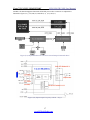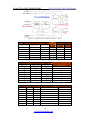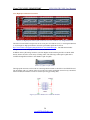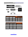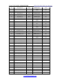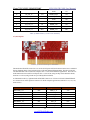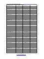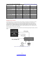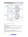
1
Virtex™ -5 LX330T/FX200T/SX240T
HTG-V5-PCIE-XXX User Manual
HiTech Global Virtex™-5 LX330T/FX200T/SX240T Multi Purpose Development Platform
PCI Express® or Stand-Alone Modes
HTG-V5-PCIE-XXX User Manual
www.HiTechGlobal.com
Version 1.4 June 2008
Copyright © HiTech Global 2002-2008
HTG-V5-PCIE-330
HTG-V5-PCIE-200
HTG-V5-PCIE-240
Doc # HTG-DOC-902
1
www.HiTechGlobal.com
Virtex™ -5 LX330T/FX200T/SX240T
HTG-V5-PCIE-XXX User Manual
HiTech Global does not assume any liability arising out of the application or use of any product described or shown
herein; nor does it convey any license under its patents, copyrights, or mask work rights or any rights of others. HiTech
Global reserves the right to make changes, at any time, in order to improve reliability and functionality of this product.
HiTech Global will not assume responsibility for the use of any circuitry described herein other than circuitry entirely
embodied in its products. HiTech Global provides any design, code, or information shown or described herein "as is."
By providing the design, code, or information as one possible implementation of a feature, application, or standard,
HiTech Global makes no representation that such implementation is free from any claims of infringement. End users
are responsible for obtaining any rights they may require for their implementation. HiTech Global expressly disclaims
any warranty whatsoever with respect to the adequacy of any such implementation, including but not limited to any
warranties or representations that the implementation is free from claims of infringement, as well as any implied
warranties of merchantability or fitness for a particular purpose.
HiTech Global will not assume any liability for the accuracy or correctness of any engineering or software support or
assistance provided to a user. HiTech Global products are not intended for use in life support appliances, devices, or
systems. Use of a HiTech Global product in such applications without the written consent of the appropriate HiTech
Global officer is prohibited.
The contents of this manual are owned and copyrighted by HiTech Global Copyright 2002-2007 HiTech Global All
Rights Reserved. Except as stated herein, none of the material may be copied, reproduced, distributed, republished,
downloaded, displayed, posted, or transmitted in any form or by any means including, but not limited to, electronic,
mechanical, photocopying, recording, or otherwise, without the prior written consent of HiTech Global. Any
unauthorized use of any material contained in this manual may violate copyright laws, trademark laws, the laws of
privacy and publicity, and communications regulations and statutes.
Revision History
Date
09/10/2007
10/08/2007
12/12/2007
2/7/2008
6/1/2008
Version
1.0
1.1
1.2
1.3
1.4
2
www.HiTechGlobal.com
Notes
Clock diagrams added
High speed connectors updated
Flash Configuration added
SX240T, FX200T info added
Virtex™ -5 LX330T/FX200T/SX240T
HTG-V5-PCIE-XXX User Manual
Table Of Contents
Chapter 1: Introduction to Viretx-5 LXTFXT/SXT
1.1) Virtex-5 FPGA General Description------------------------------------------------------------------------------1.2) Summary of Features-------------------------------------------------------------------------------------------------1.3) Supported Virtex-5 Devices ----------------------------------------------------------------------------------------1.4) RocketIO/O Multi Gigabit Transceivers (GTP/GTX) -----------------------------------------------------------1.5) End-Point Block for PCI Express-----------------------------------------------------------------------------------1.6) PowerPC 440 RISC Cores (FXT Only) --------------------------------------------------------------------------1.7) Tri-Mode Ethernet MAC --------------------------------------------------------------------------------------------1.8) Input/Output Blocks (SelectIOs) -----------------------------------------------------------------------------------1.9) Additional Virtex-5 Resources--------------------------------------------------------------------------------------Chapter 2: HTG-V5-PCIE-XXX Platform
2.1) Introduction -----------------------------------------------------------------------------------------------------2.2) System Requirement -------------------------------------------------------------------------------------------2.3) Summary Of Features ------------------------------------------------------------------------------------------2.4) Block Diagram --------------------------------------------------------------------------------------------------2.5) User I/Os & Distribution --------------------------------------------------------------------------------------2.5.1) General Purpose RocketIO GTP Ports -------------------------------------------------------2.5.2) High-Speed LVDS Samtec Connectors -----------------------------------------------------2.5.3) LED & Switches --------------------------------------------------------------------------------2.6) SO-DIMM Memory -------------------------------------------------------------------------------------------2.7) PCI Express -----------------------------------------------------------------------------------------------------2.8) Serial ATA ------------------------------------------------------------------------------------------------------2.9) Gigabit Ethernet ------------------------------------------------------------------------------------------------2.10) SMA Interface ------------------------------------------------------------------------------------------------2.11) Configuration -------------------------------------------------------------------------------------------------2.11.1) Stand Alone Mode ------------------------------------------------------------------------------2.11.2) PCI Express Mode ------------------------------------------------------------------------------2.11.3) Via PCI Express Bus ----------------------------------------------------------------------------
Chapter 3: PCI Express Software & Drivers
3.1) Introduction ----------------------------------------------------------------------------------------------------3.2) Overview --------------------------------------------------------------------------------------------------------3.3) Architecture and Operation -----------------------------------------------------------------------------------3.4) Build Instructions ----------------------------------------------------------------------------------------------Chapter 4: Intellectual Property (IP) Cores
4.1) PCI Express -----------------------------------------------------------------------------------------------------4.2) Serial ATA ------------------------------------------------------------------------------------------------------4.3) DDR 2 Memory Controller ------------------------------------------------------------------------------------
3
www.HiTechGlobal.com
Virtex™ -5 LX330T/FX200T/SX240T
HTG-V5-PCIE-XXX User Manual
Chapter 1: Introduction to Virtex-5
1.1) Virtex-5 FPGA
The Virtex®-5 family provides the newest most powerful features in the FPGA market. Using the second
generation ASMBL™ (Advanced Silicon Modular Block) column-based architecture, the Virtex-5 family
contains four distinct platforms (sub-families), the most choice offered by any FPGA family. Each platform
contains a different ratio of features to address the needs of a wide variety of advanced logic designs. In
addition to the most advanced, high-performance logic fabric, Virtex-5 FPGAs contain many hard-IP
system level blocks, including powerful 36-Kbit block RAM/FIFOs, second generation 25 x 18 DSP slices,
SelectIO™ technology with built-in digitally controlled impedance, ChipSync™ source-synchronous
interface blocks, system monitor functionality, enhanced clock management tiles with integrated DCM
(Digital Clock Managers) and phase-locked-loop (PLL) clock generators, and advanced configuration
options.
Additional platform dependant features include power-optimized high-speed serial transceiver blocks for
enhanced serial connectivity, PCI Express™ compliant integrated Endpoint blocks, tri-mode Ethernet
MACs (Media Access Controllers), and high-performance PowerPC® 440 microprocessor embedded
blocks. These features allow advanced logic designers to build the highest levels of performance and
functionality into their FPGA-based systems. Built on a 65-nm state-of-the-art copper process technology,
Virtex-5 FPGAs are a programmable alternative to custom ASIC technology. Most advanced system
designs require the programmable strength of FPGAs. Virtex-5 FPGAs offer the best solution for
addressing the needs of high-performance logic designers, high-performance DSP designers, and highperformance embedded systems designers with unprecedented logic, DSP, hard/soft microprocessor, and
connectivity capabilities. The Virtex-5 LXT, SXT, and FXT platforms include advanced high-speed serial
connectivity and link/transaction layer capability.
1.2) Summary of Features
• Four platforms LX, LXT, SXT, and FXT
− Virtex-5 LX: High-performance general logic applications
− Virtex-5 LXT: High-performance logic with advanced serial connectivity
− Virtex-5 SXT: High-performance signal processing applications with advanced serial connectivity
− Virtex-5 FXT: High-performance embedded systems with advanced serial connectivity
• Cross-platform compatibility
− LXT, SXT, and FXT devices are footprint compatible in the same package using adjustable voltage
regulators
• Most advanced, high-performance, optimal-utilization, FPGA fabric
− Real 6-input look-up table (LUT) technology
− Dual 5-LUT option
− Improved reduced-hop routing
− 64-bit distributed RAM option
− SRL32/Dual SRL16 option
• Powerful clock management tile (CMT) clocking
− Digital Clock Manager (DCM) blocks for zero delay buffering, frequency synthesis, and clock phase
shifting
− PLL blocks for input jitter filtering, zero delay buffering, frequency synthesis, and phase-matched clock
division
• 36-Kbit block RAM/FIFOs
− True dual-port RAM blocks
− Enhanced optional programmable FIFO logic
− Programmable
4
www.HiTechGlobal.com
Virtex™ -5 LX330T/FX200T/SX240T
HTG-V5-PCIE-XXX User Manual
- True dual-port widths up to x36
- Simple dual-port widths up to x72
− Built-in optional error-correction circuitry
− Optionally program each block as two independent 18- Kbit blocks
• High-performance parallel SelectIO technology
− 1.2 to 3.3V I/O Operation
− Source-synchronous interfacing using ChipSync™ technology
− Digitally-controlled impedance (DCI) active termination
− Flexible fine-grained I/O banking
− High-speed memory interface support
• Advanced DSP48E slices
− 25 x 18, two’s complement, multiplication
− Optional adder, subtracter, and accumulator
− Optional pipelining
− Optional bitwise logical functionality
− Dedicated cascade connections
• Flexible configuration options
− SPI and Parallel FLASH interface
− Multi-bitstream support with dedicated fallback reconfiguration logic
− Auto bus width detection capability
• System Monitoring capability on all devices
− On-chip/Off-chip thermal monitoring
− On-chip/Off-chip power supply monitoring
− JTAG access to all monitored quantities
• Integrated Endpoint blocks for PCI Express
− LXT, SXT, and FXT Platforms
− Compliant with the PCI Express Base Specification 1.1
− x1, x4, or x8 lane support per block
− Works in conjunction with RocketIO™ transceivers
• Tri-mode 10/100/1000 Mb/s Ethernet MACs
− LXT, SXT, and FXT Platforms
− RocketIO transceivers can be used as PHY or connect to external PHY using many soft MII (Media
Independent Interface) options
• RocketIO™ GTP transceivers 100 Mb/s to 3.75 Gb/s
− LXT and SXT Platforms
• RocketIO GTX transceivers 150 Mb/s to 6.5 Gb/s
− FXT Platform only
• PowerPC 440 Microprocessors
− FXT Platform only
− RISC architecture
− 7-stage pipeline
− 32-Kbyte instruction and data caches included
− Optimized processor interface structure (crossbar)
• 65-nm copper CMOS process technology
• 1.0V core voltage
• High signal-integrity flip-chip packaging
5
www.HiTechGlobal.com
Virtex™ 5 LX330T/ SX240T/FX200T
HTG-V5-PCIE-XXX User Manual
1.3) Supported Virtex-5 Devices
Part Number
Slices
Logic Cells
CLB Flip-Flops
Maximum Distributed RAM (Kbits)
Block RAM/FIFO w/ECC (36Kbits each)
Total Block RAM (Kbits)
Digital Clock Managers (DCM)
Phase Locked Loop (PLL)/PMCD
Maximum Single-Ended Pins
Maximum Differential I/O Pairs
DSP48E Slices
PowerPC® 440 Processor Blocks
PCI Express Endpoint Blocks
10/100/1000 Ethernet MAC Blocks
RocketIO™ GTP Low-Power Transceivers
RocketIO™ GTX High-Power Transceivers
Commercial
Industrial
Configuration Memory (Mbits)
XC5VLX330T
51,840
331,776
207,360
3,420
324
11,664
12
6
960
480
192
—
1
4
24
—
-1, -2
-1
82.7
XC5VSX240T
37,440
239,616
149,760
4,200
516
18,576
12
6
960
480
1,056
—
1
4
24
—
-1, -2
-1
79.6
XC5VFX200T
30,720
196,608
122,880
2,280
456
16,416
12
6
960
480
384
2
4
8
—
24
-1, -2
-1
70.9
1.4) RocketIO Multi Gigabit Transceivers (GTP/GTX)
GTP Transceivers (LXT/SXT only)
• Full-duplex serial transceiver capable of 100 Mb/s to 3.75 Gb/s baud rates
• 8B/10B, user-defined FPGA logic, or no encoding options
• Channel bonding support
• CRC generation and checking
• Programmable pre-emphasis or pre-equalization for the transmitter
• Programmable termination and voltage swing
• Programmable equalization for the receiver
• Receiver signal detect and loss of signal indicator
• User dynamic reconfiguration using secondary configuration bus
• Out of Band (OOB) support for Serial ATA (SATA)
• Electrical idle, beaconing, receiver detection, and PCI Express and SATA spread-spectrum clocking
support
• Less than 100 mW typical power consumption
• Built-in PRBS Generators and Checkers
RocketIO GTX Transceivers (FXT Only)
• Full-duplex serial transceiver capable of 150 Mb/s to 6.5 Gb/s baud rates
• 8B/10B encoding and programmable gearbox to support 64B/66B and 64B/67B encoding, user-defined
FPGA logic, or no encoding options
• Channel bonding support
• CRC generation and checking
• Programmable pre-emphasis or pre-equalization for the transmitter
• Programmable termination and voltage swing
• Programmable continuous time equalization for the receiver
• Programmable decision feedback equalization for the receiver
• Receiver signal detect and loss of signal indicator
• User dynamic reconfiguration using secondary configuration bus
6
www.HiTechGlobal.com
Virtex™ 5 LX330T/ SX240T/FX200T
HTG-V5-PCIE-XXX User Manual
• OOB support (SATA)
• Electrical idle, beaconing, receiver detection, and PCI Express spread-spectrum clocking support
• Low-power operation at all line rates
1.5) Integrated Endpoint Block For PCI Express
• Works in conjunction with RocketIO GTP transceivers (LXT and SXT) and GTX transceivers (FXT) to
deliver full PCI Express Endpoint functionality with minimal FPGA logic utilization.
• Conforms to the PCI Express Base Specification 1.1
• PCI Express Endpoint block or Legacy PCI Express Endpoint block
• x8, x4, x2, or x1 lane width
• Power management support
• Block RAMs used for buffering
• Fully buffered transmit and receive
• Management interface to access PCIe configuration space and internal configuration
• Support for a wide range of maximum payload size (up to 512Bytes with the Block Plus Wrapper)
• One virtual channel (VCs)
• Round robin, weighted round robin, or strict priority VC arbitration
• Up to 6 x 32 bit or 3 x 64 bit BARs (or a combination of 32 bit and 64 bit)
1.6) PowerPC 440 RISC Cores (FXT Only)
• Embedded PowerPC 440 (PPC440) cores
− Up to 550 MHz operation
− Greater than 1000 DMIPS per core
− Seven-stage pipeline
− Multiple instructions per cycle
− Out-of-order execution
− 32 Kbyte, 64-way set associative level 1 instruction cache
− 32 Kbyte, 64-way set associative level 1 data cache
− Book E compliant
• Integrated crossbar for enhanced system performance
− 128-bit Processor Local Buses (PLBs)
− Integrated scatter/gather DMA controllers
− Dedicated interface for connection to DDR2 memory controller
− Auto-synchronization for non-integer PLB-to-CPU clock ratios
• Auxiliary Processor Unit (APU) Interface and Controller
− Direct connection from PPC440 embedded block to FPGA fabric-based coprocessors
− 128-bit wide pipelined APU Load/Store
− Support of autonomous instructions: no pipeline stalls
− Programmable decode for custom instructions
1.7) Tri-Mode (10/100/1000 Mb/s) Ethernet Media Access Control (MAC)
Virtex-5 FXT/LXT/SXT devices contain four embedded Ethernet MAC blocks. The blocks have the
following characteristics:
• IEEE 802.3 compliant
• UNH-compliance tested
• MII/GMII Interface with SelectIO or SGMII interface when used with RocketIO transceivers
• Half or full duplex
• Supports Jumbo frames
• 1000 Base-X PCS/PMA: When used with RocketIO GTP transceiver, can provide complete 1000 Base-X
implementation on-chip
• DCR-bus connection to microprocessors
7
www.HiTechGlobal.com
Virtex™ 5 LX330T/ SX240T/FX200T
HTG-V5-PCIE-XXX User Manual
1.8) Input/Output Blocks (SelectIOs)
IOBs are programmable and can be categorized as follows:
• Programmable single-ended or differential (LVDS) operation
• Input block with an optional single data rate (SDR) or double data rate (DDR) register
• Output block with an optional SDR or DDR register
• Bidirectional block
• Per-bit deskew circuitry
• Dedicated I/O and regional clocking resources
• Built in data serializer/deserializer The IOB registers are either edge-triggered D-type flip-flops
or level-sensitive latches.
IOBs support the following single-ended standards:
• LVTTL
• LVCMOS (3.3V, 2.5V, 1.8V, 1.5V, and 1.2V)
• PCI (33 and 66 MHz)
• PCI-X
• GTL and GTLP
• HSTL 1.5V and 1.8V (Class I, II, III, and IV)
• HSTL 1.2V (Class 1)
• SSTL 1.8V and 2.5V (Class I and II)
The Digitally Controlled Impedance (DCI) I/O feature can be configured to provide on-chip termination for
each single-ended I/O standard and some differential I/O standards.
The IOB elements also support the following differential signaling I/O standards:
• LVDS and Extended LVDS (2.5V only)
• BLVDS (Bus LVDS)
• ULVDS
• Hypertransport™
• Differential HSTL 1.5V and 1.8V (Class I and II)
• Differential SSTL 1.8V and 2.5V (Class I and II)
• RSDS (2.5V point-to-point)
Two adjacent pads are used for each differential pair. Two or four IOB blocks connect to one switch matrix
to access the routing resources. Per-bit deskew circuitry allows for programmable signal delay internal to
the FPGA. Per-bit deskew flexibly provides fine-grained increments of delay to carefully produce a
range of signal delays. This is especially useful for synchronizing signal edges in source-synchronous
interfaces.
General purpose I/Os in select locations (eight per bank) are designed to be “regional clock capable” I/O by
adding special hardware connections for I/O in the same locality. These regional clock inputs are
distributed within a limited region to minimize clock skew between IOBs. Regional I/O clocking
supplements the global clocking resources.
1.9) Additional Virtex 5 information and documents are available at the following sites:
Virtex-5 User Guide http://direct.xilinx.com/bvdocs/userguides/ug190.pdf The Virtex™-5 User Guide
includes chapters on Clocking Resources, Clock Management Technology, Phase-Locked Loops, Block
RAM and FIFO memory, Configurable Logic Blocks (CLBs), SelectIO resources, and SelectIO™ logic
resources.
Virtex-5 XtremeDSP User Guide http://direct.xilinx.com/bvdocs/userguides/ug193.pdf This document
describes the Virtex-5 DSP48E slice.
Virtex-5 Configuration User Guide http://direct.xilinx.com/bvdocs/userguides/ug191.pdf This allencompassing configuration guide includes detailed information on the Virtex™-5 configuration interfaces
8
www.HiTechGlobal.com
Virtex™ 5 LX330T/ SX240T/FX200T
HTG-V5-PCIE-XXX User Manual
(JTAG, Serial, SelectMAP, SPI and BPI), and it discusses flows and techniques for bitstream encryption,
readback and reconfiguration.
Virtex-5 Packaging and Pinout Specification http://direct.xilinx.com/bvdocs/userguides/ug195.pdf This
user guides describes Virtex™-5 device pinouts and package specifications, and pinout diagrams and
thermal data.
Virtex-5 RocketIO GTP Transceiver User Guide http://direct.xilinx.com/bvdocs/userguides/ug196.pdf
This guide describes the RocketIO™ GTP transceivers available in the Virtex-5 LXT platform devices.
Virtex-5 RocketIO GTX Transceiver User Guide
http://www.xilinx.com/support/documentation/user_guides/ug198.pdf
This guide describes the RocketIO™ GTP transceivers available in the Virtex-5 FXT platform devices.
LogiCORE IP Endpoint Block Plus for PCI Express User Guide
http://www.xilinx.com/support/documentation/ip_documentation/pcie_blk_plus_ug341.pdf
This guide describes the functionality of the Endpoint Block Plus wrapper for PCI Express using the
Integrated Endpoint Block for PCI Express available in the Virtex-5 LXT/SXT/FXT devices.
Virtex-5 Embedded Tri-Mode Ethernet MAC User Guide
http://direct.xilinx.com/bvdocs/userguides/ug194.pdf This guide describes the dedicated Tri-Mode Ethernet
Media Access Controller (MAC) available in the Virtex™-5 LXT platform devices.
Virtex-5 System Monitor User Guide http://direct.xilinx.com/bvdocs/userguides/ug192.pdf This guide
describes the System Monitor functionality available in all Virtex™-5 devices.
Virtex-5 PCB Designer's Guide http://direct.xilinx.com/bvdocs/userguides/ug203.pdf This guide provides
information on PCB design for Virtex™-5 devices, with a focus on strategies for making design decisions
at the PCB and interface level.
9
www.HiTechGlobal.com
Virtex™ 5 LX330T/ SX240T/FX200T
HTG-V5-PCIE-XXX User Manual
Figure (1) Virtex-5 LX330T FF1738 SelectI/O Package Diagram
10
www.HiTechGlobal.com
Virtex™ 5 LX330T/ SX240T/FX200T
HTG-V5-PCIE-XXX User Manual
Figure (2) Virtex-5 LX330T FF1738 Pin Diagram
11
www.HiTechGlobal.com
Virtex™ 5 LX330T/ SX240T/FX200T
HTG-V5-PCIE-XXX User Manual
Chapter 2: Virtex-5 PCI-Express LX330T/SX240T/FX200T Platform
2.1) Introduction
The HTG-V5-PCIE-XXX board is powered by Xilinx Virtex-5 LX330T, SX240T, or FX200T FPGA
which offers 24 RocketIO™ GTP/GTX Transceivers, up to 8 hard-coded Gigabit Ethernet Media Access
Controllers (MAC) , up to four x8 PCI Express End-Point Block, up to two PPC440 processors, and more
than 331,000 FPGA logic cells.
The HTG-V5-PCIE-XXX provides wide variety of connectors and interfaces including:
-
PCI Express 8-lane upstream
x2 Gigabit Ethernet with SGMII support (using x2 RocketIO transceivers)
x2 SATA Connectors
x10 General Purpose RocketIO GTP/GTX transceivers with adjustable Reference Clock
x8 SMA (connected to two RocketIO GTP/GTX channels)
x2 Samtec with 68 pairs of LVDS (2.5V) or 136 Single-ended (3.3V) - for any customized or
off-the-shelf modules such as FPGA expansion, DVI, USB, etc.)
x1 200-pin DDR-2 SO-DIMM (up to 2 GB)
x1 256 Mb Intel Flash – for configuration or data storage
The HTG-V5-PCIE-XXX can be used either as Stand-Alone or PCI Express based card. This provides
additional functionality and cost saving so designers can use the same board for multiple designs, projects,
and applications. JP11 and JP43 can be used to switch between PCI Express and Stand-alone mode:
PCI Express Mode Æ J11: “Removed” (turns ON the U18 regulator) & J43 “Placed” (when the
board is plugged into PCI Express slot)
Stand-alone Mode Æ J11: “Placed” (turns OFF the U18 regulator) & J43 “Removed” (when the
board is in stand alone mode and powered by an external 5 V supply)
Notes: The U18 is used to convert the 12V supply (from PC motherboard) to 5V. The output of this regulator is fed to U14, U15,
U16, and U17 for conversion to 1.0V, 2.5V, 1.8V, and 3.3V
Picture (1) PCIe/Stand Alone Setting
The feature-rich Virtex-5 LXT/SXT/FXT and availability of more than 100 different IP Cores through
HiTech Global, and variety of different connectors and interfaces, make the HTG-V5-PCIE-XXX an
extremely versatile platform for serial interface, embedded system, and storage designs. A complete list of
IP Cores supported by HiTech Global is available at http://www.hitechglobal.com/ipcores/
The Virtex-5 HTG-V5-PCIE-XXX can be bundled and shipped with evaluation version of the following IP
Cores:
- DDR 2 Memory Controller http://www.hitechglobal.com/IPCores/DDR2Controller.htm
- SATA http://hitechglobal.com/ipcores/sata.htm
- PCI Express Back-End (Provides a high-performance DMA Engine and a simplified user interface)
12
www.HiTechGlobal.com
Virtex™ 5 LX330T/ SX240T/FX200T
HTG-V5-PCIE-XXX User Manual
2.2) System Requirements
- HTG-V5-PCIE-XXX Board
- PCI Express Based Mother Board (for PCI Express based developments) – Not required if the
HTG-V5-PCIE-XXX is used as “stand alone”. The following PC Mother board with multiple
PCIe slots is available through HiTech Global http://hitechglobal.com/Accessories/PC.htm (with
installed PCIECV test, Windows drivers, and interface GUI)
- Xilinx ISE Foundation 10.1
2.3) Summary of Features
► Xilinx Virtex-5 LX330T, SX240, or FX200T FPGA (FF1738 package)
► 8-Lane PCI Express End-Point (upstream) Connector
► Up to 2 GB of SO-DIMM DDR2 Memory (the SO-DIMM socket is populated on the flip side)
► 2 RocketIO GTP/GTX Ports accessible through 8 SMA connectors (4 Rx & 4 Tx)
► 10 Reference-Clock-Adjustable RocketIO GTP/GTX Ports accessible through two high-speed Samtec
QSE connectors - ideal to host add-on modules such as PCI Express Root port, SFP, SATA, etc.
► 64 Pairs of 2.5V LVDS IOs or 128 Single-ended 3.3V IOs accessible via two independent high speed
Samtec connectors
► 2 SATA Ports (I/II)
► 2 Gigabit Ethernet Ports (both with SGMII support)
► PCI Express Jitter Attenuator with adjustable clock outputs
► Super Clocks with adjustable outputs for the SATA and RocketIO GTP/GTX ports
► External Clock input
► 256 Mb Intel Flash Memory (for FPGA configuration and additional user Flash storage)
► ATX and Standard 5V Power Connectors
► Jumpers for Stand Alone mode
► Jumper for FPGA configuration via PCIe bus
13
www.HiTechGlobal.com
Virtex™ 5 LX330T/ SX240T/FX200T
HTG-V5-PCIE-XXX User Manual
2.4) Block Diagram & Dimensions
Figure (3) illustrates the overall components placement and dimensions of the HTG-V5-PCIE-XXX board.
Figure (3): HTG-V5-PCIE-XXX Components Placement
14
www.HiTechGlobal.com
Virtex™ 5 LX330T/ SX240T/FX200T
HTG-V5-PCIE-XXX User Manual
15
www.HiTechGlobal.com
Virtex™ 5 LX330T/ SX240T/FX200T
HTG-V5-PCIE-XXX User Manual
2.5) User I/O & Distribution
The on-board Virtex-5 (XC5VLX330T/SX240T/FX200T-FF1738) provides total of 960 user I/Os which
have been used for connection of different peripherals and components to the FPGA device.
Figure (4) illustrates distribution and allocation of the XC5VLX330T-FF1738 user I/Os (Virtex-5 SX240T
and FX200T devices have the same number of Select and RocektIOs)
Figure (4) User I/O Allocation & Distribution
2.5.1) General Purpose Data-Rate-Adjustable RocketIO GTP/GTX Ports
The HTG-V5-PCIE-XXX board provides access to 10 Reference-Clock-Adjustable RocketIO Gigabit
Transceiver (GTP/GTX) ports through two high-speed Samtec connectors (J14 and J15 with part number
QSE-020-01-X-D-A http://www.samtec.com/ftppub/pdf/QSE.PDF ). Each connector provides access to 5
RocketIO GTP/GTX ports. This makes the HTG-V5-PCIE-XXX a flexible platform for all SerialIO
16
www.HiTechGlobal.com
Virtex™ 5 LX330T/ SX240T/FX200T
HTG-V5-PCIE-XXX User Manual
standards. The data throughputs of RocketIO GTP/GTX ports on these connectors are adjustable as
illustrated in figure (5.a) , (5.b) and (5.c) and table (1.a), (1.b), and (1.c).
Figure (5.a) Adjustable Reference Clock for General Purpose RocketIO Ports
Figure (5.b) Input/output Frequency Scheme – Step 1
17
www.HiTechGlobal.com
Virtex™ 5 LX330T/ SX240T/FX200T
HTG-V5-PCIE-XXX User Manual
Figure (5.c) Input/output Frequency Scheme – Step 2
M2
(SW3: 6th key)
Inputs
M1
(SW3: 5th key)
M0
(SW3: 4th key)
M
Divider
Value
Minimum
Maximum
0
0
0
18
31.1
38.9
0
0
1
22
25.5
31.8
0
1
0
24
23.3
29.2
0
1
1
25
22.4
28.0
1
0
0
32
17.5
21.9
1
Input Frequency (MHz)
0
1
40
14.0
Table (1.a) ICS843001 (U2) Programmable “M” Output Divider Function Table
N2
(SW3: 3rd key)
Inputs
N1
(SW3: 2nd key)
N0
(SW3: 1st key)
M Divider Value
0
0
0
1
0
0
1
2
0
1
0
3
0
1
1
4
1
0
0
5
1
0
1
6
1
1
0
8
1
1
1
10
Table (1.b) ICS843001 (U2) Programmable “N” Output Divider Function Table
F_SEL2
Inputs
F_SEL1
F_SEL0
0
0
0
2÷
2÷
1
0
0
5÷
2÷
0
1
0
4÷
2÷
1
1
0
2÷
4÷
0
0
1
2÷
5÷
1
0
1
5÷
4÷
0
1
1
4÷
5÷
1
17.5
Outputs
QA0/nQA0, QA0/nQA0
1
1
4÷
Table (1.c ) ICS874003 (U12) F_SEL[2:0] Function Table
18
www.HiTechGlobal.com
QB0/nQB0
4÷
Virtex™ 5 LX330T/ SX240T/FX200T
HTG-V5-PCIE-XXX User Manual
Connector # J14 (Lower)
Connector
Pin #
1
3
5
7
9
11
13
15
17
19
21
23
25
27
29
31
33
34
37
39
Signal Name
MGTTXP0_132
MGTTXN0_132
GND0
MGTRXP0_132
MGTRXN0_132
GND1
MGTRXP1_132
MGTRXN1_132
GND2
MGTTXP1_132
MGTTXN1_132
GND3
MGTTXP0_128
MGTTXN0_128
GND4
NC
NC
GND5
GTP_CLCK0_P
GTP_CLCK0_N
FPGA Pin
#
B18
B17
A17
A16
A14
A15
B13
B14
B12
B11
Connector
Pin #
2
4
6
8
10
12
14
16
18
20
22
24
26
28
30
32
34
36
38
40
Signal Name
MGTRXP0_128
MGTRXN0_128
GND6
MGTRXP1_128
MGTRXN1_128
GND7
MGTTXP1_128
MGTTXN1_128
GND8
MGTTXP0_124
MGTTXN0_124
GND9
MGTRXP0_124
MGTRXN0_124
GND10
NC
NC
GND11
NC
NC
FPGA
Pin #
A11
A10
A8
A9
B7
B8
B6
B5
A5
A4
Connector # J15 (Upper)
Connector
Pin #
1
3
5
7
9
11
13
15
17
19
21
23
25
27
29
31
33
34
37
39
FPGA Pin
Connector
Signal Name
#
Pin #
Signal Name
MGTRXP1_124
A2
2
MGTTXP1_116
MGTRXN1_124
A3
4
MGTTXN1_116
GND0
6
GND6
MGTTXP1_124
B1
8
MGTTXP0_120
MGTTXN1_124
B2
10
MGTTXN0_120
GND1
12
GND7
MGTTXP0_116
K2
14
MGTRXP0_120
MGTTXN0_116
L2
16
MGTRXN0_120
GND2
18
GND8
MGTRXP0_116
L1
20
MGTRXP1_120
MGTRXN0_116
M1
22
MGTRXN1_120
GND3
24
GND9
MGTRXP1_116
P1
26
MGTTXP1_120
MGTRXN1_116
N1
28
MGTTXN1_120
GND4
30
GND10
NC
32
NC
NC
34
NC
36
GND5
GND11
GTP_CLK2_P
38
NC
GTP_CLK2_N
40
NC
Table (2) Distribution of General Purpose RocketIO Ports.
19
www.HiTechGlobal.com
FPGA
Pin #
R2
P2
D2
E2
E1
F1
H1
G1
J2
H2
Virtex™ 5 LX330T/ SX240T/FX200T
HTG-V5-PCIE-XXX User Manual
2.5.2) High-Speed SelectI/O Connectors
Picture (2) High-Speed Samtec QSE Connectors for 2.5V LVDS or 3.3V Single-Ended IOs
The HTG-V5-PCIE-XXX board provides access to 68 pairs of LVDS IOs (2.5V) or 136 Single-Ended IOs
(3.3V) through two high-speed Samtec connectors (part number QSE-060-01-F-D-A
http://www.samtec.com/ftppub/cpdf/QSE-XXX-01-X-D-XXX-MKT.pdf ). The dedicated IO banks’
voltages are set via the J26 jumper (bank# 19, 20, 23, and 24)
In addition to the QTE mating connectors (used on daughter cards interfacing the HTG-V5-PCIE-XXX
board), Samtec also offers wide variety of mating cables. The following 6-inche QSE to QSE cable is
available through HiTech Global : (Part Number: QSE-TO-QSE)
Picture (3) QSE To QSE Cable
The high speed connectors can be used for connecting add-on modules to the HTG-V5-PCIE-XXX board.
The J25 header with 3.3V and J24 with 5.0V provide power supply and higher current for any customized
add-on module (these headers can also be used for powering up cooling fans).
Figure (6) Power Headers For Add-On Modules
20
www.HiTechGlobal.com
Virtex™ 5 LX330T/ SX240T/FX200T
HTG-V5-PCIE-XXX User Manual
Dedicated differential clocks are available on both J15 and J16 connectors. Figure (7) illustrates the clock
control circuit.
Figure (7) Adjustable Reference Clock for High Speed Connectors
M2
(SW4: 6th key)
Inputs
M1
(SW4: 5th key)
M0
(SW4: 4th key)
M
Divider
Value
Input Frequency (MHz)
Minimum
Maximum
0
0
0
18
31.1
38.9
0
0
1
22
25.5
31.8
0
1
0
24
23.3
29.2
0
1
1
25
22.4
28.0
1
0
0
32
17.5
21.9
1
0
1
40
14.0
17.5
Table (3.a) ICS843001 (U3) Programmable “M” Output Divider Function Table
N2
(SW4: 3rd key)
Inputs
N1
(SW4: 2nd key)
N0
(SW4: 1st key)
M Divider Value
0
0
0
1
0
0
1
2
0
1
0
3
0
1
1
4
1
0
0
5
1
0
1
6
1
1
0
8
1
1
1
10
Table (3.b) ICS843001 (U3) Programmable “N” Output Divider Function Table
21
www.HiTechGlobal.com
Virtex™ 5 LX330T/ SX240T/FX200T
HTG-V5-PCIE-XXX User Manual
Table (4.a) and (4.b) illustrate pin assignment for each high-speed connector.
Connector # J16 (Lower)
Connector
Pin #
2
4
6
8
10
12
14
16
18
20
22
24
26
28
30
32
34
36
38
40
42
44
46
48
50
52
54
56
58
60
Connector
Pin Name
LVDS0_P
LVDS0_N
GND0
LVDS1_P
LVDS1_N
GND1
LVDS2_P
LVDS2_N
GND2
LVDS3_P
LVDS3_N
GND3
LVDS4_P
LVDS4_N
GND4
LVDS5_P
LVDS5_N
GND5
LVDS6_P
LVDS6_N
LVDS7_P
LVDS7_N
GND7
PWR0
PWR1
GND8
PWR2
PWR3
GND9
LVDS8_P
62
LVDS8_N
64
66
68
70
72
74
76
78
80
82
GND10
PWR4
PWR5
GND11
LVDS9_P
LVDS9_N
GND12
LVDS10_P
LVDS10_N
GND13
Signal
Name
LVDS0_P
LVDS0_N
GND
LVDS1_P
LVDS1_N
GND
LVDS2_P
LVDS2_N
GND
LVDS3_P
LVDS3_N
GND
LVDS4_P
LVDS4_N
GND
LVDS5_P
LVDS5_N
GND
LVDS6_P
LVDS6_N
LVDS7_P
LVDS7_N
GND
LVDS66_P
LVDS66_N
GND
VCCO
VCCO
GND
DIFFCLK
0_P
DIFFCLK
0_N
GND
VCCO
VCCO
GND
LVDS8_P
LVDS8_N
GND
LVDS9_P
LVDS9_N
GND
FPGA
Pin #
N33
N34
J16
Connector
Pin Name
LVDS17_P
LVDS17_N
GND21
LVDS18_P
LVDS18_N
GND22
LVDS19_P
LVDS19_N
GND23
LVDS20_P
LVDS20_N
GND24
LVDS21_P
LVDS21_N
GND25
LVDS22_P
LVDS22_N
GND26
LVDS23_P
LVDS23_N
LVDS24_P
LVDS24_N
GND27
PWR6
PWR7
GND28
PWR8
PWR9
GND29
LVDS25_P
Connector
Pin #
1
3
5
7
9
11
13
15
17
19
21
23
25
27
29
31
33
35
37
39
41
43
45
47
49
51
53
55
57
59
J15
LVDS25_N
61
N35
M36
GND30
PWR10
PWR11
GND31
LVDS26_P
LVDS26_N
GND32
LVDS27_P
LVDS27_N
GND33
63
65
67
69
71
73
75
77
79
81
M34
M33
M32
M31
G32
G31
H34
G34
F35
E35
E32
E33
K33
J33
L36
L35
22
www.HiTechGlobal.com
Signal
Name
LVDS16_P
LVDS16_N
GND
LVDS17_P
LVDS17_N
GND
LVDS18_P
LVDS18_N
GND
LVDS19_P
LVDS19_N
GND
LVDS20_P
LVDS20_N
GND
LVDS21_P
LVDS21_N
GND
LVDS22_P
LVDS22_N
LVDS23_P
LVDS23_N
GND
LVDS64_P
LVDS64_N
GND
VCC2V5
VCC2V5
GND
DIFFCLK1_
P
DIFFCLK1_
N
GND
VCC2V5
VCC2V5
GND
LVDS24_P
LVDS24_N
GND
LVDS25_P
LVDS25_N
GND
FPGA
Pin #
N31
P31
G33
H33
H31
J31
E34
F34
F31
F32
K32
J32
P33
P32
T32
U32
M26
L27
N36
P36
K35
J35
Virtex™ 5 LX330T/ SX240T/FX200T
84
86
88
90
92
94
96
98
100
102
104
106
108
110
112
114
116
118
120
GND14
LVDS11_P
LVDS11_N
GND15
LVDS12_P
LVDS12_N
GND16
LVDS13_P
LVDS13_N
GND17
LVDS14_P
LVDS14_N
GND18
LVDS15_P
LVDS15_N
GND19
LVDS16_P
LVDS16_N
GND20
GND
LVDS10_P
LVDS10_N
GND
LVDS11_P
LVDS11_N
GND
LVDS12_P
LVDS12_N
GND
LVDS13_P
LVDS13_N
GND
LVDS14_P
LVDS14_N
GND
LVDS15_P
LVDS15_N
GND
HTG-V5-PCIE-XXX User Manual
H35
J36
U34
T35
U36
V36
F37
E37
E38
D37
V33
W33
GND34
LVDS28_P
LVDS28_N
GND35
LVDS29_P
LVDS29_N
GND36
LVDS30_P
LVDS30_N
GND37
LVDS31_P
LVDS31_N
GND38
LVDS32_P
LVDS32_N
GND39
LVDS33_P
LVDS33_N
GND40
83
85
87
89
91
93
95
97
99
101
103
105
107
109
111
113
115
117
119
GND
LVDS26_P
LVDS26_N
GND
LVDS27_P
LVDS27_N
GND
LVDS28_P
LVDS28_N
GND
LVDS29_P
LVDS29_N
GND
LVDS30_P
LVDS30_N
GND
LVDS31_P
LVDS31_N
T34
U33
R35
T36
F36
G36
V35
V34
Y33
W32
Y32
AA32
Table (4.a) High-Speed LVDS Connectors Summary – Connector # 1 (lower)
Connector # 17 (Upper)
Connector
Pin #
2
4
6
8
10
12
14
16
18
20
22
24
26
28
30
32
34
36
38
40
42
44
46
Connector
Pin Name
LVDS0_P
LVDS0_N
GND0
LVDS1_P
LVDS1_N
GND1
LVDS2_P
LVDS2_N
GND2
LVDS3_P
LVDS3_N
GND3
LVDS4_P
LVDS4_N
GND4
LVDS5_P
LVDS5_N
GND5
LVDS6_P
LVDS6_N
LVDS7_P
LVDS7_N
GND7
Signal
Name
LVDS32_P
LVDS32_N
GND
LVDS33_P
LVDS33_N
GND
LVDS34_P
LVDS34_N
GND
LVDS35_P
LVDS35_N
GND
LVDS36_P
LVDS36_N
GND
LVDS37_P
LVDS37_N
GND
LVDS38_P
LVDS38_N
LVDS39_P
LVDS39_N
GND
FPGA
Pin #
J12
H11
G12
G11
F12
F11
E10
F10
K14
K13
K12
J11
J13
H13
H10
J10
Connector
Pin Name
LVDS17_P
LVDS17_N
GND21
LVDS18_P
LVDS18_N
GND22
LVDS19_P
LVDS19_N
GND23
LVDS20_P
LVDS20_N
GND24
LVDS21_P
LVDS21_N
GND25
LVDS22_P
LVDS22_N
GND26
LVDS23_P
LVDS23_N
LVDS24_P
LVDS24_N
GND27
23
www.HiTechGlobal.com
Connector
Pin #
1
3
5
7
9
11
13
15
17
19
21
23
25
27
29
31
33
35
37
39
41
43
45
Signal
Name
LVDS48_P
LVDS48_N
GND
LVDS49_P
LVDS49_N
GND
LVDS50_P
LVDS50_N
GND
LVDS51_P
LVDS51_N
GND
LVDS52_P
LVDS52_N
GND
LVDS53_P
LVDS53_N
GND
LVDS54_P
LVDS54_N
LVDS55_P
LVDS55_N
GND
FPGA
Pin #
H14
H15
K10
L10
L12
L11
G13
G14
F14
E13
N11
P12
E12
D12
P11
N10
Virtex™ 5 LX330T/ SX240T/FX200T
48
50
52
54
56
58
60
62
64
66
68
70
72
74
76
78
80
82
84
86
88
90
92
94
96
98
100
102
104
106
108
110
112
114
116
118
120
HTG-V5-PCIE-XXX User Manual
PWR0
PWR1
GND8
PWR2
PWR3
GND9
LVDS8_P
LVDS67_P
PWR6
47
LVDS65_P
LVDS67_N
PWR7
49
LVDS65_N
GND
GND28
51
GND
VCCO
PWR8
53
VCC2V5
VCCO
PWR9
55
VCC2V5
GND
GND29
57
GND
DIFFCLK2_
L29
LVDS25_P
59
DIFFCLK3_
P
P
LVDS8_N
DIFFCLK2_
K28
LVDS25_N
61
DIFFCLK3_
N
N
GND10
GND
GND30
63
GND
PWR4
VCCO
PWR10
65
VCC2V5
PWR5
VCCO
PWR11
67
VCC2V5
GND11
GND
GND31
69
GND
LVDS9_P
LVDS40_P
V9
LVDS26_P
71
LVDS56_P
LVDS9_N
LVDS40_N
V10
LVDS26_N
73
LVDS56_N
GND12
GND
GND32
75
GND
LVDS10_P
LVDS41_P
F9
LVDS27_P
77
LVDS57_P
LVDS10_N
LVDS41_N
G9
LVDS27_N
79
LVDS57_N
GND13
GND
GND33
81
GND
GND14
GND
GND34
83
GND
LVDS11_P
LVDS42_P
G7
LVDS28_P
85
LVDS58_P
LVDS11_N
LVDS42_N
G8
LVDS28_N
87
LVDS58_N
GND15
GND
GND35
89
GND
LVDS12_P
LVDS43_P
U8
LVDS29_P
91
LVDS59_P
LVDS12_N
LVDS43_N
U9
LVDS29_N
93
LVDS59_N
GND16
GND
GND36
95
GND
LVDS13_P
LVDS44_P
T10
LVDS30_P
97
LVDS60_P
LVDS13_N
LVDS44_N
T11
LVDS30_N
99
LVDS60_N
GND17
GND
GND37
101
GND
LVDS14_P
LVDS45_P
J8
LVDS31_P
103
LVDS61_P
LVDS14_N
LVDS45_N
J7
LVDS31_N
105
LVDS61_N
GND18
GND
GND38
107
GND
LVDS15_P
LVDS46_P
U11
LVDS32_P
109
LVDS62_P
LVDS15_N
LVDS46_N
V11
LVDS32_N
111
LVDS62_N
GND19
GND
GND39
113
GND
LVDS16_P
LVDS47_P
K8
LVDS33_P
115
LVDS63_P
LVDS16_N
LVDS47_N
K9
LVDS33_N
117
LVDS63_N
GND20
GND
GND40
119
GND
Table (4.b) High-Speed LVDS Connectors Summary – Connector # 2 (Upper)
24
www.HiTechGlobal.com
L16
L15
B5
F5
R9
T9
F7
F6
R7
R8
D7
E7
P7
P8
E9
E8
N9
N8
Virtex™ 5 LX330T/ SX240T/FX200T
HTG-V5-PCIE-XXX User Manual
2.5.3) LED, Switches, & Push Buttons
The HTG-V5-PCIE-XXX is populated with one user DIP Switch (SW5), eight user LEDs, 3 Push Buttons
(user Reset, PCIE Reset, and PCIE Wake). Table (5) illustrates the FPGA pin assignment.
FPGA Signal Name
IO_L0P_25
IO_L0N_25
IO_L1P_25
IO_L1N_25
IO_L2P_25
IO_L2N_25
IO_L3P_25
IO_L3N_25
IO_L4P_25
IO_L4N_VREF_25
IO_L5P_25
IO_L5N_25
IO_L6P_25
IO_L6N_25
IO_L7P_25
IO_L7N_25
IO_L8P_CC_25
IO_L8N_CC_25
IO_L9P_CC_25
Signal Name
SW0 (SW5 Switch)
SW1 (SW5 Switch)
SW2 (SW5 Switch)
SW3 (SW5 Switch)
SW4 (SW5 Switch)
SW5 (SW5 Switch)
SW6 (SW5 Switch)
SW7 (SW5 Switch)
LED0 (DS14)
LED1 (DS15)
LED2 (DS16)
LED3 (DS17)
LED4 (DS18)
LED5 (DS19)
LED6 (DS20)
LED7 (DS21)
USR_RESET
PCIE_PERST_#
PCIEWAKE_#
FPGA Pin #
AG31
AF31
AF32
AG33
AH33
AG32
AH31
AJ31
AV35
AV36
AU36
AT35
AU34
AT34
AR35
AR34
AU32
AU33
AV33
Table (5) LED & Switches Connections Summary
2.6) DDR 2 SO-DIMM
Picture (4) DDR2 SODIMM
The HTG-V5-PCIE-XXX board is populated with a 200-pin SO-DIMM connector which supports
installation of Dual-Rank DDR2 SDRAM SO-DIMMs up to 2 GB (DDR2-533 and/or DDR2-400)
DDR-2 Memory Controller IP Core is available through HiTech Global. Additional information is
available at http://www.hitechglobal.com/IPCores/DDR2Controller.htm
Connector Pin Numbers/Pin Names, Signal Names, FPGA Pin Numbers, and used Banks are summarized
in Table (6)
25
www.HiTechGlobal.com
Virtex™ 5 LX330T/ SX240T/FX200T
Bank
FPGA Pin Description
FPGA Pin
Number
HTG-V5-PCIE-XXX User Manual
Signal Name
SO-DIMM
Connector Pin
VCC0V9_VTT
1
GND
2
GND
3
13
IO_L17N_13
AT42
DIMM_DQ4
4
13
IO_L15N_13
AN41
DIMM_DQ0
5
13
IO_L19P_13
AU42
DIMM_DQ5
6
13
IO_L17P_13
AR42
DIMM_DQ1
7
GND
8
GND
9
13
IO_L15P_13
AM41
DIMM_DM0
10
13
IO_L11N_CC_13
AC39
DIMM_DQS0_N
11
GND
12
13
IO_L11P_CC_13
AC40
DIMM_DQS0_P
13
13
IO_L4P_13
AF40
DIMM_DQ6
14
GND
15
13
IO_L6N_SM3N_13
AJ41
DIMM_DQ7
16
13
IO_L13N_13
AK42
DIMM_DQ2
17
GND
18
13
IO_L13P_13
AL41
DIMM_DQ3
19
13
IO_L0N_SM8N_13
AB42
DIMM_DQ12
20
GND
21
13
IO_L0P_SM8P_13
AB41
DIMM_DQ13
22
13
IO_L6P_SM3P_13
AJ42
DIMM_DQ8
23
GND
24
13
IO_L1N_SM7N_13
AD42
DIMM_DQ9
25
13
IO_L1P_SM7P_13
AC41
DIMM_DM1
26
GND
27
GND
28
13
IO_L8N_CC_SM1N_13
AB38
DIMM_DQS1_N
29
13
IO_L10P_CC_13
AE40
DIMM_CLK0_P
30
13
IO_L8P_CC_SM1P_13
AB37
DIMM_DQS1_P
31
13
IO_L10N_CC_13
AD40
DIMM_CLK0_N
32
GND
33
GND
34
13
IO_L2P_SM6P_13
AE42
DIMM_DQ10
35
13
IO_L3P_SM5P_13
AF41
DIMM_DQ14
36
26
www.HiTechGlobal.com
Virtex™ 5 LX330T/ SX240T/FX200T
HTG-V5-PCIE-XXX User Manual
13
IO_L2N_SM6N_13
AD41
DIMM_DQ11
37
13
IO_L3N_SM5N_13
AF42
DIMM_DQ15
38
GND
39
GND
40
GND
41
GND
42
13
IO_L7N_SM2N_13
AJ40
DIMM_DQ16
43
13
IO_L5P_SM4P_13
AG42
DIMM_DQ20
44
13
IO_L14P_13
AL42
DIMM_DQ17
45
13
IO_L5N_SM4N_13
AH41
DIMM_DQ21
46
GND
47
GND
48
DIMM_DQS2_N
49
NC
50
13
IO_L9N_CC_SM0N_13
AC38
13
IO_L9P_CC_SM0P_13
AB39
DIMM_DQS2_P
51
13
IO_L7P_SM2P_13
AH40
DIMM_DM2
52
GND
53
GND
54
13
IO_L16P_13
AP42
DIMM_DQ18
55
13
IO_L18N_13
AU41
DIMM_DQ22
56
13
IO_L18P_13
AT41
DIMM_DQ19
57
13
IO_L16N_13
AP41
DIMM_DQ23
58
GND
59
GND
60
11
IO_L13N_11
R40
DIMM_DQ24
61
11
IO_L13P_11
P41
DIMM_DQ28
62
11
IO_L15P_SM13P_11
T42
DIMM_DQ25
63
11
IO_L15N_SM13N_11
U41
DIMM_DQ29
64
GND
65
GND
66
11
IO_L8N_CC_11
Y40
DIMM_DM3
67
11
IO_L9N_CC_11
AA39
DIMM_DQS3_N
68
NC
69
DIMM_DQS3_P
70
GND
71
GND
72
11
IO_L9P_CC_11
AA40
11
IO_L6N_11
N41
DIMM_DQ26
73
11
IO_L11P_CC_SM14P_11
Y37
DIMM_DQ30
74
11
IO_L8P_CC_11
W40
DIMM_DQ27
75
27
www.HiTechGlobal.com
Virtex™ 5 LX330T/ SX240T/FX200T
11
IO_L11N_CC_SM14N_11
AA37
11
11
17
IO_L0N_11
IO_L9N_CC_17
G42
AT40
HTG-V5-PCIE-XXX User Manual
DIMM_DQ31
76
GND
77
GND
78
DIMM_CKE
79
DIMM_CKE
80
VCC1V8
81
VCC1V8
82
NC
83
NC
84
DIMM_BA2
85
NC
86
VCC1V8
87
VCC1V8
88
17
IO_L6N_17
AG38
DIMM_A12
89
17
IO_L6P_17
AF39
DIMM_A11
90
17
IO_L5P_17
AE39
DIMM_A9
91
17
IO_L3N_17
AD37
DIMM_A7
92
17
IO_L4P_17
AE37
DIMM_A8
93
17
IO_L3P_17
AD36
DIMM_A6
94
VCC1V8
95
VCC1V8
96
17
IO_L2N_17
AD35
DIMM_A5
97
17
IO_L2P_17
AC36
DIMM_A4
98
17
IO_L1N_17
AB36
DIMM_A3
99
17
IO_L1P_17
AC35
DIMM_A2
100
17
IO_L0N_17
AC34
DIMM_A1
101
17
IO_L0P_17
AB34
DIMM_A0
102
VCC1V8
103
VCC1V8
104
17
IO_L5N_17
AE38
DIMM_A10
105
17
IO_L9P_CC_17
AR40
DIMM_BA1
106
17
IO_L8N_CC_17
AP40
DIMM_BA0
107
11
IO_L2P_11
H41
DIMM_RAS_N
108
11
IO_L1P_11
F41
DIMM_WE_N
109
11
IO_L6P_11
M42
DIMM_S0_N
110
VCC1V8
111
VCC1V8
112
11
IO_L1N_11
G41
DIMM_CAS_N
113
11
IO_L0P_11
F42
DIMM_ODT
114
28
www.HiTechGlobal.com
Virtex™ 5 LX330T/ SX240T/FX200T
HTG-V5-PCIE-XXX User Manual
11
IO_L7N_11
P40
DIMM_S1_N
115
17
IO_L8P_CC_17
AN40
DIMM_A13
116
VCC1V8
117
VCC1V8
118
DIMM_ODT
119
NC
120
GND
121
GND
122
11
IO_L16N_SM12N_11
V41
DIMM_DQ32
123
11
IO_L17N_SM11N_11
W41
DIMM_DQ36
124
11
IO_L19P_SM9P_11
AA42
DIMM_DQ33
125
11
IO_L18N_SM10N_11
Y42
DIMM_DQ37
126
GND
127
GND
128
11
IO_L10N_CC_SM15N_11
Y38
DIMM_DQS4_N
129
11
IO_L19N_SM9N_11
AA41
DIMM_DM4
130
11
IO_L10P_CC_SM15P_11
Y39
DIMM_DQS4_P
131
GND
132
GND
133
11
IO_L16P_SM12P_11
U42
DIMM_DQ38
134
11
IO_L14P_11
T40
DIMM_DQ34
135
11
IO_L17P_SM11P_11
V40
DIMM_DQ39
136
11
IO_L18P_SM10P_11
W42
DIMM_DQ35
137
GND
138
GND
139
15
IO_L0N_15
H39
DIMM_DQ44
140
15
IO_L17N_15
Y34
DIMM_DQ40
141
15
IO_L17P_15
AA34
DIMM_DQ45
142
15
IO_L18N_15
W35
DIMM_DQ41
143
GND
144
GND
145
15
IO_L10N_CC_15
J40
DIMM_DQS5_N
146
15
IO_L19P_15
W36
DIMM_DM5
147
15
IO_L10P_CC_15
H40
DIMM_DQS5_P
148
GND
149
GND
150
15
IO_L19N_15
W37
DIMM_DQ42
151
15
IO_L16P_15
AA35
DIMM_DQ46
152
15
IO_L18P_15
Y35
DIMM_DQ43
153
29
www.HiTechGlobal.com
Virtex™ 5 LX330T/ SX240T/FX200T
15
IO_L16N_15
AA36
HTG-V5-PCIE-XXX User Manual
DIMM_DQ47
154
GND
155
GND
156
15
IO_L13N_15
U38
DIMM_DQ48
157
15
IO_L13P_15
T37
DIMM_DQ52
158
15
IO_L15N_15
W38
DIMM_DQ49
159
15
IO_L15P_15
V39
DIMM_DQ53
160
GND
161
GND
162
NC
163
DIMM_CLK1_P
164
GND
165
15
IO_L8P_CC_15
M38
15
IO_L8N_CC_15
L39
DIMM_CLK1_N
166
15
IO_L9N_CC_15
J38
DIMM_DQS6_N
167
GND
168
15
IO_L9P_CC_15
K38
DIMM_DQS6_P
169
15
IO_L14P_15
T39
DIMM_DM6
170
GND
171
GND
172
15
IO_L1P_15
G38
DIMM_DQ50
173
15
IO_L6P_15
P38
DIMM_DQ54
174
15
IO_L7N_15
M39
DIMM_DQ51
175
15
IO_L6N_15
N38
DIMM_DQ55
176
GND
177
GND
178
15
IO_L7P_15
N39
DIMM_DQ56
179
15
IO_L1N_15
G39
DIMM_DQ60
180
15
IO_L4P_15
R39
DIMM_DQ57
181
15
IO_L5P_15
R37
DIMM_DQ61
182
GND
183
GND
184
15
IO_L5N_15
P37
DIMM_DM7
185
15
IO_L11N_CC_15
K39
DIMM_DQS7_N
186
GND
187
15
IO_L11P_CC_15
K40
DIMM_DQS7_P
188
15
IO_L3P_15
E39
DIMM_DQ58
189
GND
190
15
IO_L3N_15
E40
DIMM_DQ59
191
15
IO_L2N_15
F40
DIMM_DQ62
192
30
www.HiTechGlobal.com
Virtex™ 5 LX330T/ SX240T/FX200T
HTG-V5-PCIE-XXX User Manual
GND
193
15
IO_L2P_15
F39
DIMM_DQ63
194
11
IO_L7P_11
N40
DIMM_SDA
195
GND
196
11
IO_L5P_11
L42
DIMM_SCL
197
11
IO_L2N_11
J41
DIMM_SA0
198
VCC1V8
199
DIMM_SA1
200
11
IO_L5N_11
M41
Table (6) DDR2 Memory Connections Summary
2.7) PCI Express
Picture (5) 8-Lane PCI Express End-Point
The RocketIO GTP/GTX Transceivers are used as PCI Express PHY and connected to the hard –coded PCI
Express Endpoint block of the on-board Virtex 5 LX330T/SX240T/FX200T FPGA. The HTG-V5-PCIE330 and 240 boards can be used for PCI Express Gen 1 x1/x2/x4/x8 End-Point applications. The HTG-V5PCIE-200 board can be used for PCI Express Gen 1 x1/x2/x4/x8 (using on-chip hard-coded PCIe block)
and Gen 2 x1/x2/x4 (using soft IP core provided by HiTech Global)
As illustrated in table (7), eight RocketIO GTP/GTX Transceivers of Virtex-5 LX330T/SX240T/FX200T
are connected to an 8-lane upstream connector for PCIE end point applications (GTP/GTX: 118, 122, 126,
and 130 tiles)
Pin Description
MGTTXP0_118
MGTAVTTTX_118
MGTTXN0_118
MGTRXP0_118
MGTAVTTRX_118
MGTRXN0_118
MGTAVCCPLL_118
MGTRXN1_118
FPGA Pin Number
Signal Name
PCIe Connector Pin
AH2
AH3
AJ2
AJ1
AJ3
AK1
AM3
AL1
PER0_C_P
AVTTTX_118
PER0_C_N
PET0_P
AVTTRX_118
PET0_N
AVCCPLL_118
PET1_N
A16
31
www.HiTechGlobal.com
A18
B14
B15
B20
Virtex™ 5 LX330T/ SX240T/FX200T
MGTREFCLKN_118
MGTRXP1_118
MGTREFCLKP_118
MGTTXN1_118
MGTAVTTTX_118
MGTTXP1_118
MGTTXP0_122
MGTAVTTTX_122
MGTTXN0_122
MGTRXP0_122
MGTAVTTRX_122
MGTRXN0_122
MGTAVCCPLL_122
MGTRXN1_122
MGTREFCLKN_122
MGTRXP1_122
MGTREFCLKP_122
MGTTXN1_122
MGTAVTTTX_122
MGTTXP1_122
MGTTXP0_126
MGTAVTTTX_126
MGTTXN0_126
MGTRXP0_126
MGTAVTTRX_126
MGTRXN0_126
MGTAVCCPLL_126
MGTRXN1_126
MGTREFCLKN_126
MGTRXP1_126
MGTREFCLKP_126
MGTTXN1_126
MGTAVTTTX_126
MGTTXP1_126
MGTTXP0_130
MGTAVTTTX_130
MGTTXN0_130
MGTRXP0_130
MGTAVTTRX_130
MGTRXN0_130
MGTAVCCPLL_130
MGTRXN1_130
MGTREFCLKN_130
MGTRXP1_130
AK3
AM1
AK4
AM2
AN3
AN2
AP2
AP3
AR2
AR1
AR3
AT1
AV3
AU1
AT3
AV1
AT4
AV2
AW3
AW2
BA1
AY1
BA2
BB2
AY2
BB3
AY5
BB4
AY4
BB5
AW4
BA5
AY6
BA6
BA7
AY12
BA8
BB8
AY8
BB9
AY11
BB10
AY9
BB11
HTG-V5-PCIE-XXX User Manual
PCIECLK1_N
PET1_P
PCIECLK1_P
PER1_C_N
AVTTTX_118
PER1_C_P
PER2_C_P
AVTTTX-122
PER2_C_N
PET2_P
AVTTRX-122
PET2_N
AVCCPLL_122
PET3_N
NC
PET3_P
NC
PER3_C_N
AVTTTX-122
PER3_C_P
PER4_C_P
AVTTTX_126
PER4_C_N
PET4_P
AVTTRX_126
PET4_N
AVCCPPL_126
PET5_N
PCIECLK0_N
PET5_P
PCIECLK0_P
PER5_C_N
AVTTTX_126
PER5_C_P
PER6_C_P
AVTTTX-130
PER6_C_N
PET6_P
AVTTRX-130
PET6_N
AVCCPLL-130
PET7_N
NC
PET7_P
32
www.HiTechGlobal.com
B19
A22
A21
A25
A26
B23
B24
B28
B27
A30
A29
A35
A36
B33
B34
B38
B37
A40
A39
A43
A44
B41
B42
B46
B45
Virtex™ 5 LX330T/ SX240T/FX200T
MGTREFCLKP_130
MGTTXN1_130
MGTAVTTTX_130
MGTTXP1_130
MGTAVCC_118
MGTAVCC_118
MGTAVCC_122
MGTAVCC_122
MGTAVCC_126
MGTAVCC_126
MGTAVCC_130
MGTAVCC_130
HTG-V5-PCIE-XXX User Manual
AW9
NC
BA11
PER7_C_N
AY7
AVTTTX-130
BA12
PER7_C_P
AL3
AVCC_118
AL4
AVCC_118
AU3
AVCC_122
AU4
AVCC_122
AW5
AVCC_126
AY3
AVCC_126
AW10
AVCC_130
AY10
AVCC_130
Table (7) PCI Express Upstream Connections Summary
A48
A47
PCI Express Jitter Attenuator
An IDT ICS874003-02 is used as PCI Express Jitter Attenuator on the HTG-V5-PCIE-XXX board. This
chip is a high performance Differential- to-LVDS Jitter Attenuator designed for use in PCI Express
systems. In some PCI Express systems, such as those found in desktop PCs, the PCI Express clocks are
generated from a low bandwidth, high phase noise PLL frequency synthesizer. In these systems, a jitter
attenuator may be required to attenuate high frequency random and deterministic jitter components from
the PLL synthesizer and from the system board.
Figures (8) and Table (8) illustrate the implementation of the attenuator chip and output frequency selection
modes.
Figure (8) PCI Express Jitter Attenuator Diagram
33
www.HiTechGlobal.com
Virtex™ 5 LX330T/ SX240T/FX200T
HTG-V5-PCIE-XXX User Manual
Picture (9) PCIe Jitter Attenuator Control
F_SEL2
0
1
0
1
0
1
0
1
INPUT
OUTPUT
F_SEL1
F_SEL0
QA0/nQA0, QA1/nQA1
0
0
DIV2
0
0
DIV5
1
0
DIV4
1
0
DIV2
0
1
DIV2
0
1
DIV5
1
1
DIV4
1
1
DIV4
Table (8) PCI Express Jitter Attenuator Mode Select
2.8) Serial ATA (SATA)
Picture (10) SATA Connector
The HTG-V5-PCIE-XXX board supports two SATA (I & II) ports via RocketIO GTP/GTX 112 tile.
An ICS843001-21 Frequency Synthesizer used with the SATA ports. As shown in Table (6), applying
different input frequencies along with different selections of “M” and “N” Divider values generates
different output frequencies that can used for SATA and other applications. The default crystal values are
25 MHz & 10 MHz (selected by the J2 jumper) . Additional GTP/GTX reference clock frequencies can be
generated by inserting different oscillators into the X6 socket and positioning the SW2 switch (SATA
Super Clock).
The clock circuit diagram for the SATA connectors is illustrated in figure (9).
34
www.HiTechGlobal.com
Virtex™ 5 LX330T/ SX240T/FX200T
HTG-V5-PCIE-XXX User Manual
Figure (9) Adjustable Reference Clock for SATA Ports
Table (9.a) and 9(.b) should be used for selection of “M” and “N” output dividers:
M2
(SW2: 6th key)
Inputs
M1
(SW2: 5th key)
M0
(SW2: 4th key)
M
Divider
Value
Input Frequency (MHz)
Minimum
Maximum
0
0
0
18
31.1
38.9
0
0
1
22
25.5
31.8
0
1
0
24
23.3
29.2
0
1
1
25
22.4
28.0
1
0
0
32
17.5
21.9
1
0
1
40
14.0
17.5
Table (9.a) ICS843001 (U13) Programmable “M” Output Divider Function Table
N2
(SW2: 3rd key)
Inputs
N1
(SW2: 2nd key)
N0
(SW2: 1st key)
M Divider Value
0
0
0
1
0
0
1
2
0
1
0
3
0
1
1
4
1
0
0
5
1
0
1
6
1
1
0
8
1
1
1
10
Table (9.b) ICS843001 (U13) Programmable “N” Output Divider Function Table
35
www.HiTechGlobal.com
Virtex™ 5 LX330T/ SX240T/FX200T
FPGA Pin Description
HTG-V5-PCIE-XXX User Manual
FPGA Pin Number
MGTTXP0_112
SATA Connector
SATA_Host_TX0-P
T2
AA3
AVTTTX_112
MGTTXN0_112
U2
SATA_Host_TX0-N
MGTRXP0_112
U1
SATA_Host_RX0-P
MGTAVTTRX_112
U3
AVTTRX_112
MGTRXN0_112
V1
SATA_Host_RX0-N
MGTAVCCPLL_112
Y3
AVCCPLL_112
MGTRXN1_112
W1
SATA_Host_RX1-N
MGTREFCLKN_112
V3
SUPPERCLKA_Q0-GTP_N
MGTRXP1_112
Y1
SATA_Host_RX1-P
MGTREFCLKP_112
V4
SUPPERCLKA_Q0-GTP_P
MGTTXN1_112
Y2
SATA_Host_TX1_N
MGTAVTTTX_112
T3
AVTTTX_112
MGTTXP1_112
AA2
SATA_Host_RX1-P
MGTAVTTRXC
AA5
VTTRXC
MGTAVTTTX_112
AVTTTX_112
AB4
Table (10) SATA Pin Description
MGTRREF_112
SATA Host and Device IP Cores are available through HiTech Global. Additional information is available
at http://www.hitechglobal.com/ipcores/sata.htm
Input Reference
Clock
M Divider
Value
N Divider
Value
VCO
(MHz)
25
25
26.5625
24
24
24
4
8
6
600
600
637.5
26.5625
26.5625
Output
Frequency
(MHz)
150
75
106.25
Applications
SATA
SATA
Fibre Channel 1
4 Gig Fibre
24
3
637.5
212.5
Channel
10 Gig Fibre
Channel
24
4
637.5
159.375
Table (11) ICS (Frequency Synthesizer) Common Configuration
36
www.HiTechGlobal.com
Virtex™ 5 LX330T/ SX240T/FX200T
HTG-V5-PCIE-XXX User Manual
2.9) 10/100/1000 Tri-Speed Ethernet PHY
Picture (11) Gigabit Ethernet RJ45 Connectors
The HTG-V5-PCIE-XXX board is populated with two Marvell Alaska PHY devices (88E1111) operating
at 10/100/1000 Mb/s.
The Marvell Alaska PHY device enables copper 1000BASE-T Gigabit Interface Converter (GBIC)
modules as well as Small Form Factor Pluggable (SFP) modules. The single-port Alaska family offers
additional support of 1000BASE-X through an integrated 1.25 GHz Serializer /Deserializer (SERDES),
enabling the use of the device in fiber-optic Gigabit Ethernet applications (IEEE 802.3z). The Marvell
Alaska devices include advanced features such as:
•
•
•
•
•
Virtual Cable Tester™ (VCT) cable diagnostic
Media Detect feature
Low power consumption
Small footprint
2/3-Pair Downshift
Bank
12
12
12
12
12
12
12
12
12
12
FPGA Pin Description
IO_L0P_12
IO_L0N_12
IO_L1P_12
IO_L1N_12
IO_L2P_12
IO_L2N_12
IO_L3P_12
IO_L3N_12
IO_L4P_12
IO_L4N_VREF_12
FPGA Pin Number
AA7
AA6
G6
H5
W5
W6
H6
J5
Y7
W7
37
www.HiTechGlobal.com
PHY “A” Pins
PHYA_TXD0
PHYA_TXD1
PHYA_TXD2
PHYA_TXD3
PHYA_TXD4
PHYA_TXD5
PHYA_TXD6
PHYA_TXD7
PHYA_TXEN
PHYA_TXER
Virtex™ 5 LX330T/ SX240T/FX200T
12
12
IO_L5P_12
IO_L5N_12
12
12
12
12
12
12
12
12
12
12
12
12
12
12
12
12
12
12
12
12
12
12
12
12
12
12
12
12
IO_L6P_12
IO_L6N_12
IO_L7P_12
IO_L7N_12
IO_L8P_CC_12
IO_L8N_CC_12
IO_L9P_CC_12
IO_L9N_CC_12
IO_L10P_CC_12
IO_L10N_CC_12
IO_L11P_CC_12
IO_L11N_CC_12
IO_L12P_VRN_12
IO_L12N_VRP_12
IO_L13P_12
IO_L13N_12
IO_L14P_12
IO_L14N_VREF_12
IO_L15P_12
IO_L15N_12
IO_L16P_12
IO_L16N_12
IO_L17P_12
IO_L17N_12
IO_L18P_12
IO_L18N_12
IO_L19P_12
IO_L19N_12
MGTTXP1_114
MGTTXN1_114
MGTRXP1_114
MGTRXN1_114
HTG-V5-PCIE-XXX User Manual
J6
K5
W8
V8
K4
L5
V5
V6
L6
M6
N5
N6
U7
U6
P5
P6
T7
T6
R4
R5
T5
T4
AA11
AA10
AA9
Y10
W11
W10
Y9
Y8
AG2
AF2
AF1
AE1
PHYA_INT
PHYA_MDC
PHYA_RESET
PHYACRS
PHYA_COL
PHYA_MDIO
PHYA_TXCLK
NC
PHYA_GTXCLK
NC
PHYA_RXCLK
NC
NC
NC
VRN_12
VRN_12
NC
NC
NC
NC
PHYA_RXDO
PHYA_RXD1
PHYA_RXD2
PHYA_RXD3
PHYA_RXD4
PHYA_RXD5
PHYA_RXD6
PHYA_RXD7
PHYA_RXDV
PHYA_RXER
PHYA_TXP
PHYA_TXN
PHYA_RXP
PHYA_RXN
Table (12) PHY “A” Pin Assignment
The HTG-V5-PCIE-XXX board supports MII, GMII, RGMII, and SGMIII interface modes with the FPGA.
The PHYs are connected to two hard-coded 10/100/1000 Ethernet Media Access Controllers (MACs)
inside the Virtex-5 FPGA. Two RocketIO GPT/GTX ports have also been used to support SMII interface.
The other sides of PHYs are connected to two Halo HFJ11-1G01E RJ-45 (Eth A and Eth B) Connectors
with built-in magnetic.
A 25-MHz crystal supplies the clock signal to the PHY. The PHY is configured to default at power-on or
reset (these settings may be overwritten via software). I/O connections to the Ethernet PHY are
summarized in Table (11)
38
www.HiTechGlobal.com
Virtex™ 5 LX330T/ SX240T/FX200T
HTG-V5-PCIE-XXX User Manual
Pin
CONFIG0
Bit[2]
PHYADR[2]
Bit[1]
PHYADR[1]
Bit[0]
PHYADR[0]
000
CONFIG1
ENA_PAUSE
PHYADR[4]
PHYADR[3]
000
CONFIG2
ANEG[3]
ANEG[2]
ANEG[1]
111
CONFIG3
ANEG[0]
ENA_XC
DIS_125
111
CONFIG4
HWCFG_MODE[2]
HWCFG_MODE[1]
HWCFG_MODE[0]
111
CONFIG5
DIS_FC
DIS_SLEEP
HWCFG_MODE[3]
111
CONFIG6
SEL_BDT
INT_POL
75/50 OHM
010
Table (13) PHY “A” & “B” Configuration
Pin to Constant Mapping
Pin
VCC2V5
PHY_LED_LINK10
Bit[2:0]
111
110
PHY_LED_LINK100
101
PHY_LED_LINK1000
PHY_LED_DUPLEX
PHY_LED_RX
100
011
010
PHY_LED_TX
001
GND
000
Table (14) Pin To Constant Mapping
39
www.HiTechGlobal.com
PHY Address
"00000". Do not
advertise the
PAUSE bit
Auto-Neg enabled,
advertise all
capabilities; prefer
slave. Auto
crossover enabled.
125 CLK option
disabled.
GMII to Cu mode.
Fiber/copper autodetect disabled.
Sleep mode
disabled.
MDC/MDIO
selected. Active
LOW Interrupt.
50Ohm SERDES
option.
Virtex™ 5 LX330T/ SX240T/FX200T
HTG-V5-PCIE-XXX User Manual
10/100/1000 Ethernet Jumper Setting:
PHY "A”:
Figure (10) PHY “A” Jumper Setting
PHY “B”:
Figure (11) PHY “A” Jumper Setting
Bank
18
18
18
18
18
18
18
18
18
18
FPGA Pin Description
IO_L0P_18
IO_L0N_18
IO_L1P_18
IO_L1N_18
IO_L2P_18
IO_L2N_18
IO_L3P_18
IO_L3N_18
IO_L4P_18
IO_L4N_VREF_18
FPGA Pin Number
PHY “B” Pins
AJ7
AK7
AB11
AC10
AL5
AK5
AB9
AB8
AJ6
AJ5
PHYB_TXD0
40
www.HiTechGlobal.com
PHYB_TXD1
PHYB_TXD2
PHYB_TXD3
PHYB_TXD4
PHYB_TXD5
PHYB_TXD6
PHYB_TXD7
PHYB_TXEN
PHYB_TXER
Virtex™ 5 LX330T/ SX240T/FX200T
18
18
18
18
18
18
18
18
18
18
18
18
18
18
18
18
18
18
18
18
18
18
18
18
18
18
18
18
18
18
IO_L5P_18
IO_L5N_18
IO_L6P_18
IO_L6N_18
IO_L7P_18
IO_L7N_18
IO_L8P_CC_18
IO_L8N_CC_18
HTG-V5-PCIE-XXX User Manual
AC8
AC9
AH6
AH5
AD10
AD11
AG4
IO_L9P_CC_18
IO_L9N_CC_18
IO_L10P_CC_18
IO_L10N_CC_18
IO_L11P_CC_18
IO_L11N_CC_18
IO_L12P_VRN_18
IO_L12N_VRP_18
IO_L13P_18
IO_L13N_18
IO_L14P_18
IO_L14N_VREF_18
IO_L15P_18
IO_L15N_18
IO_L16P_18
IO_L16N_18
IO_L17P_18
IO_L17N_18
IO_L18P_18
IO_L18N_18
IO_L19P_18
IO_L19N_18
MGTTXP0_114
MGTTXN0_114
MGTRXP0_114
MGTRXN0_114
AH4
AB7
AB6
AC5
AC6
AF5
AF6
AD6
AD7
AG6
AG7
AE5
AD5
AF7
AE7
AD8
AE8
AF9
AF10
AE9
AE10
AF11
AF12
AC1
AD1
AB2
AC2
Table (15) PHY “B” Pin Assignment
41
www.HiTechGlobal.com
PHYB_INT
PHYB_MDC
PHYB_RESET
PHYB_CRS
PHYB_COL
PHYB_MDIO
PHYB_TXCLK
NC
PHYB_GTXCLK
NC
PHYB_RXCLK
NC
NC
NC
VRN_18
VRN_18
NC
NC
NC
NC
PHYB_RXD0
PHYB_RXD1
PHYB_RXD2
PHYB_RXD3
PHYB_RXD4
PHYB_RXD5
PHYB_RXD6
PHYB_RXD7
PHYB_RXDV
PHYB_RXER
PHYB_TXP
PHYB_TXN
PHYB_RXP
PHYB_RXN
Virtex™ 5 LX330T/ SX240T/FX200T
HTG-V5-PCIE-XXX User Manual
2.10) SMA Interface
Picture (12) SMA Connectors
Two RocketIO GTP/GTX ports are connected to 8 SMA connectors (TxN, TxP, RxN, and RxP). The
GTP/GTX reference clock is provided externally through J36 and J38 SMA connectors. The following
conversion modules can be used in conjunction with the SMA connectors:
Picture (13) SMA to SFP
Picture (14) SMA to SATA
Picture (15) SMA to HSSDC2
Picture (16)SMA to RJ45
SMA to SMA cables are available through HiTech Global (Part Number: SMA-CBL2)
Connector Pin Name
SMA_TX0_P
SMA_TX0_N
SMA_RX0_P
SMA_RX0_N
SMA_RX1_N
SMA_RX1_P
SMA_TX1_N
SMA_TX1_P
SMA_MGT_CLK_N
SMA_MGT_CLK_P
Signal Name
MGTTXP0_134
MGTTXN0_134
MGTRXP0_134
MGTRXN0_134
MGTRXN1_134
MGTRXP1_134
MGTTXN1_134
MGTTXP1_134
MGTREFCLKN_134
MGTREFCLKP_134
FPGA Pin #
BA13
BA14
BB14
BB15
BB17
BB16
BA18
BA17
AW16
AY15
Table (16) SMA Connectors Pin Assignment
2.11) Configuration Options
The on-board FPGA can be configured “direct” or via “Platform Flash”.
2.11.1) Direct FPGA Configuration
1) As illustrated in Figure (12), connect the 14-pin header of the Xilinx USB programming cable to
the “J1” connector. The USB header should be connected to USB port of a PC on the other side.
The Xilinx ISE (10.1 or higher) should already been installed on the PC.
2) Apply 5V / 5+ Amp supply either to the “J12” (standard wall power supply) OR “J18” (ATX
Power Connector). Note: Applying higher supply voltages will damage the board.
3) Turn the “SW1” switch “ON”. The voltage LEDs ,located at the bottom of the board, should
illuminate after applying the power.
42
www.HiTechGlobal.com
Virtex™ 5 LX330T/ SX240T/FX200T
HTG-V5-PCIE-XXX User Manual
Picture (12) Configuration in Stand Alone Mode
4) Launch the ISE 10.1 “iMPACT” tool:
Start → All Programs → Xilinx ISE → Accessories → iMPACT.
5) Cancel the following window (iMPACT Project). This leads to verification of on-board Xilinx
components.
43
www.HiTechGlobal.com
Virtex™ 5 LX330T/ SX240T/FX200T
HTG-V5-PCIE-XXX User Manual
6) Double Click on the “Boundary Scan” (the first item on the list) and Single Click on the
“Initialize Chain” icon (the 7th icon from the left on the tool bar). This verifies correct connection
between the board and PC by identifying the on-board Xilinx components in the chain (Platform
Flash and FPGA).
Additional reading for Boundary Scan:
Virtex-5 devices support IEEE standards 1149.1 and 1532. IEEE 1532 is a standard for In-System
Configuration (ISC), based on the IEEE 1149.1 standard. JTAG is an acronym for the Joint Test Action
Group, the technical subcommittee initially responsible for developing the standard. This standard provides
a means to ensure the board-level integrity of individual components and the interconnections between
them. The IEEE 1149.1 Test Access Port and Boundary-Scan Architecture is commonly referred to as
JTAG. With multi-layer PC boards becoming increasingly dense and more sophisticated surface
mounting techniques in use, Boundary-Scan testing is becoming widely used as an important debugging
tool.
Devices containing Boundary-Scan logic can send data out on I/O pins in order to test connections between
devices at the board level. The circuitry can also be used to send signals internally to test the devicespecific behavior. These tests are commonly used to detect opens and shorts at both the board and device
level.
In addition to testing, Boundary-Scan offers the flexibility for a device to have its own set of user-defined
instructions. The added common vendor-specific instructions, such as configure and verify, have increased
the popularity of Boundary-Scan testing and functionality.
Additional information is available at: http://direct.xilinx.com/bvdocs/userguides/ug191.pdf
44
www.HiTechGlobal.com
Virtex™ 5 LX330T/ SX240T/FX200T
HTG-V5-PCIE-XXX User Manual
Platform Flash Programming:
.
BPI Mode Jumper Setting
http://www.xilinx.com/support/documentation/application_notes/xapp973.pdf
45
www.HiTechGlobal.com
Application Note: Virtex-5 FPGAs
Indirect Programming of BPI PROMs with
Virtex-5 FPGAs
R
XAPP973 (v1.2) February 6, 2008
Summary
Author: Stephanie Tapp
Support for direct configuration from parallel NOR flash memory (BPI PROMs) is included on
Virtex™-5 Platform FPGAs, creating an attractive solution for high-density designs. To support this
new configuration mode, iMPACT has added indirect programming support for select BPI PROMs
during prototyping. This application note demonstrates how to program a Intel StrataFlash P30
BPI PROM indirectly using iMPACT 9.2i and a Xilinx cable. In this solution, the Virtex-5 FPGA
serves as a bridge between the IEEE STD 1149.1 (JTAG) bus interface and the BPI bus interface.
The required hardware setup, BPI-UP PROM file generation flow, and BPI indirect programming
flow are shown. The Virtex-5 FPGA BPI-UP configuration sequence is also described.
Note: Parallel NOR flash memory is referred to by the term BPI PROM throughout this document.
Introduction
Xilinx FPGAs are CMOS configurable latch (CCL) based and must be configured at power-up
from a non-volatile source. FPGA configuration is traditionally accomplished with a JTAG
interface, a microprocessor, or the Xilinx PROMs (Platform Flash PROMs). In systems where
the easiest solution is preferred, Master Serial mode with a Xilinx Platform Flash PROM is still
the most popular configuration mode because it has:
•
A direct JTAG interface for programming
•
The smallest interface pin requirement for configuration
•
Flexible I/O voltage support
Moreover, this solution is available for any Virtex-5 FPGA device (refer to [Ref 1] for more information).
In addition to the traditional methods, a direct configuration interface to third-party BPI PROMs
is included on Virtex-5 FPGAs to address changing system requirements. Systems with a BPI
PROM already on-board for random-access, non-volatile application data storage can benefit
from consolidating the configuration storage into the same memory device.
Similar to the traditional configuration memories, BPI PROMs must be loaded with the
configuration data. BPI PROMs have a single interface for programming, and three primary
methods to deliver the data to this interface:
•
Third-party programmers (off-board programming)
•
In-system programming (ISP) with an embedded processor
•
Indirect ISP (using JTAG or custom solution)
Production programming is often accomplished off-board with a third-party programmer or insystem with a JTAG tool vendor. During the prototyping phase, indirect ISP is preferred to easily
accommodate design iterations. The iMPACT 9.2i software, included in the Xilinx ISE™
development software tools, provides indirect programming for select BPI PROMs.
Because BPI PROMs do not have a JTAG interface, extra logic is required to serve as a bridge
between the iMPACT programmer (using a cable to drive the JTAG bus interface), and the BPI
PROM (connected to the FPGA's BPI bus interface). This extra logic must be downloaded into
the FPGA by iMPACT before indirect programming is possible.
This application note is divided into three main sections. The first section discusses the
hardware connections required for the indirect in-system programming of BPI PROMs for
prototype designs. The second section shows the Xilinx software tool flows for generating a
PROM file formatted for 16-bit BPI-UP mode and then for programming the select BPI PROMs.
© 2007–2008 Xilinx, Inc. All rights reserved. XILINX, the Xilinx logo, and other designated brands included herein are trademarks of Xilinx, Inc. PowerPC is a trademark of IBM
Corp. and is used under license. All other trademarks are the property of their respective owners.
XAPP973 (v1.2) February 6, 2008
www.xilinx.com
46
R
Introduction
The third section provides a basic configuration flow overview for the FPGA after the BPI
PROM is programmed and describes expectations when using this indirect setup.
iMPACT Indirect In-System Programming with a Virtex-5 FPGA
The basic hardware setup required for the iMPACT indirect BPI PROM programming method is
shown in Figure 1.
X-Ref Target - Figure 1
iMPACT
R
Platform Cable USB
Model DLC9
Power 5V
0.26A
Serial UH - 12345
Made in U.S.A.
2mm
CONNECTOR
SIGNALS
Virtex-5 FPGA with
JTAG-to-BPI Bitstream
STATUS
Gnd
BPI PROM
JTAG or Serial
---INIT
------TDI
DIN
TDO DONE
TCK
CCLK
TMS PROG
Vref
Vref
JTAG Bus
1.5 < Vref < 5.0 VDC
BPI Bus
ADAPTER
X973_01_020608
Figure 1:
iMPACT Indirect BPI PROM Programming with a Virtex-5 FPGA
Minimum Requirements
•
Virtex-5 FPGA (programming support for 16-bit data width only)
•
BPI PROM (refer to Table 1)
•
Xilinx Cable and Connector (refer to Table 4, page 6)
•
ISE iMPACT Software 9.2i
Selecting BPI PROMs
Several factors are considered when selecting a BPI PROM (including BPI PROM family,
density, package, and the data bus width). When using iMPACT 9.2i for programming, the BPI
PROM family must be selected from the supported list in Table 1.
Table 1: BPI PROM Programming Capability with iMPACT
BPI PROM Vendor(1)
Intel
Family(2)
Density
StrataFlash Embedded P30 (28FxxxP30)
64–256 Mb
Embedded J3 v. D (28FxxxJ3)(3)
32–128 Mb
Notes:
1.
2.
3.
XAPP973 (v1.2) February 6, 2008
Refer to “Software Flows for BPI File Preparation and Programming,” page 8 for more information.
If another revision of the listed Intel flash families are being used, please refer to the vendor's data sheet
for any differences.
iMPACT supports only the 16-bit data bus width for indirect programming via Virtex-5 FPGA family members.
www.xilinx.com
47
R
Introduction
After the BPI PROM family is selected, consider the BPI PROM density. All of the Virtex-5 FPGAs
can be configured from a single BPI PROM (typical configuration density requirements for
Virtex-5 FPGAs are provided in Table 2). A larger BPI PROM can be used for daisy-chained
applications, storing multiple FPGA configuration bitstreams, or for applications storing additional
user data, such as code for embedded MicroBlaze™ core or embedded PowerPC™ processors.
Table 2: Typical Virtex-5 FPGA Configuration Bit Requirements
Xilinx FPGA
Configuration Bits
(Per Device)
Smallest BPI PROM
Required
XC5VLX30
8,374,016
8 Mb
XC5VLX50
12,556,672
16 Mb
XC5VLX85
21,845,632
32 Mb
XC5VLX110
29,124,608
32 Mb
XC5VLX155(1)
41,048,064
64 Mb
XC5VLX220
53,139,456
64 Mb
XC5VLX330
79,704,832
128 Mb
XC5VLX20T(1)
6,251,200
8 Mb
XC5VLX30T
9,371,136
16 Mb
XC5VLX50T
14,052,352
16 Mb
XC5VLX85T
23,341,312
32 Mb
XC5VLX110T
31,118,848
32 Mb
XC5VLX155T(1)
43,042,304
64 Mb
XC5VLX220T
55,133,696
64 Mb
XC5VLX330T
82,696,192
128 Mb
XC5VSX35T
13,349,120
16 Mb
XC5VSX50T
20,019,328
32 Mb
XC5VSX95T
35,716,096
64 Mb
Notes:
1.
Indirect BPI programming support for the newest Virtex-5 FPGA family members is included in iMPACT 9.2.04i.
The other BPI PROM features: package, and the data bus width, also need to be considered
when using iMPACT.
This application note highlights a setup and software flow for a Intel StrataFlash JS28F256P30T
BPI PROM. If another package is selected, please refer to the vendor's data sheet for any signal
connection variations.
Caution! iMPACT supports only the 16-bit data bus mode for BPI PROM programming with Virtex-5
FPGAs. If the Intel Embedded J3 v. D family is chosen, the data bus must be connected for the 16-bit
mode to be programmed with iMPACT.
Hardware for BPI PROM Indirect Programming
Figure 2, page 4 shows a typical hardware setup used for Virtex-5 FPGA BPI configuration and
indirect BPI PROM programming. When configuring a Virtex-5 FPGA in the BPI configuration mode,
the setup typically consists of a master device (FPGA) and a slave device (BPI PROM). Refer to the
“Virtex-5 FPGA Configuration from BPI PROMs ,” page 22 for details on the configuration
sequence of the FPGA after the BPI PROM is successfully programmed. Although Virtex-5
FPGAs support both 8-bit and 16-bit data bus width access for configuration, the 16-bit mode is
highlighted because the iMPACT BPI PROM programming only supports the 16-bit data bus width.
XAPP973 (v1.2) February 6, 2008
www.xilinx.com
48
R
Introduction
In BPI configuration mode, the Virtex-5 FPGA configures itself from an industry-standard
parallel NOR Flash PROM, as illustrated in Figure 2.
X-Ref Target - Figure 2
Ribbon Cable Header for FPGA
JTAG Configuration
NC
NC
TDI
TDO
TCK
TMS
VREF
(+3.3V)
•
D[15:0]
4.7 kΩ
•
+3.3V
•
1 kΩ
Pushbutton
RS[1:0](7)
•
VSS
+3.3V
330Ω
PROG_B
CLK
ADV
RST
+3.3V
INIT_B
IO_L9P_CC_GC_4(8)
WP
WAIT
CE
OE
WE
DQ[15:0]
A[24:1]
A[23:0]
4.7 kΩ
Virtex-5
FPGA
VPP
•
VCCQ
•
+3.3V
+3.3V
4.7 kΩ
4.7 kΩ
4.7 kΩ
4.7 kΩ
+1.8V
VCC
M0
VCCINT
M2
M1
+3.3V
FCS_B
FOE_B
FWE_B
Jumper
Mode
Selection
(BPI_UP)(5)
VCCO_4(4)
VCCO_2(3)
VCCO_1(2)
VCC_CONFIG(1)
VCCAUX
TMS
TCK
TDO
TDI
+1.0V
+3.3V
+2.5V
Intel SrataFlash
JS28F256P30
BPI PROM
CSO_B(7)
LED
CCLK
HSWAPEN(6)
DONE
GND
•
X973_02_020608
Notes:
1.
2.
3.
4.
5.
6.
7.
8.
VCC_CONFIG (VCCO_0) is the configuration output supply voltage and supplies the dedicated configuration pins: TMS, TCK, TDO, TDI,
M[2:0], HSWAPEN, PROG_B, DONE, INIT_B, CCLK, D_IN.
VCCO_1 supplies A[19:0].
VCCO_2 supplies FCS_B, FOE_B, FWE_B, A[25:20], and D[0:7].
VCCO_4 supplies D[8:15].
It is recommended to have the option for both JTAG (M[2:0] = 101) and BPI_UP (M[2:0] = 010) configuration modes.
HSWAPEN can be driven Low to enable pull-ups on I/O.
RS[1:0] and CSO_B signals are used for advanced daisy-chain and revisioned applications. These signals are not connected for this setup.
Refer to [Ref 3] for detailed information.
IO_L9P_CC_GC_4 pin is recommended to be reserved and not connected in a design when using the iMPACT indirect programming core.
If this signal is used, the target application must consider that the iMPACT indirect programming core can drive this signal Low.
Caution! The iMPACT indirect programming solution drives all FPGA address lines (A[25:0]) during ISP operations on the BPI PROM. The
FPGA address lines must be connected directly to the BPI PROM address lines. If the upper BPI PROM address signals are tied to the FPGA
RS[1:0] pins for a Fallback or Multiboot implementation, the indirect programming solution cannot erase or program the BPI PROM address
space accessed by the upper two address signals. It is necessary to jumper the FPGA RS[1:0] pins with the FPGA upper address signals to
combine the two setups.
Figure 2:
BPI Configuration Mode Setup (Master Virtex-5 FPGA and Slave BPI PROM)
XAPP973 (v1.2) February 6, 2008
www.xilinx.com
49
R
Introduction
Virtex-5 FPGA BPI Configuration Signals
The BPI configuration mode interface signals that influence the successful start and stop of data
transfer are listed in Table 3. Details on the Virtex-5 FPGA configuration sequence and powerup considerations are discussed in “Power-On Considerations for BPI Configuration,” page 22.
Table 3: Virtex-5 FPGA BPI Configuration Mode Signals and Descriptions
Virtex-5
FPGA Pin
Name
Direction
During
Configuration
ADDR[25:0](3)
Output
Description
During Configuration
After Configuration
Address output.
Connects to PROM
address inputs.
User I/O(1)
Output
(treat as I/O for
signal integrity)
Configuration clock output.
CCLK does not directly
connect to BPI PROM but
is used internally to
generate the address and
sample read data.
FPGA drives clock for
internal configuration logic.
Dedicated CCLK (user
controllable)
Output
For parallel daisy chains,
this signal is driven Low
when data is delivered to
downstream device
User I/O(1)
CSO_B
Parallel daisy chain activeLow chip select output. Not
used in single-FPGA
applications.
User I/O(1)
Input
Data input, sampled by the
rising edge of the FPGA
CCLK.
Data captured by FPGA.
D[15:0]
DONE
Active-High signal
indicating configuration is
complete:
0 = FPGA not configured
1 = FPGA configured
FPGA drives DONE Low.
Bidirectional,
Open-Drain, or
active
Active-Low Flash chip
select output.
This output is actively
driven Low. It has a weak
pull-up resistor during
configuration.
User I/O(1,2)
Active-Low Flash output
enable.
This output is actively
driven Low during
configuration and has a
weak pull-up before
configuration.
User I/O(1,2)
Active-Low Flash write
enable.
This output is actively
driven High and has a
weak pull-up during
configuration.
User I/O(1,2)
Controls I/O (except Bank
0 dedicated I/Os).
Pull-up resistors during
configuration. This pin has
a built-in weak pull-up
resistor.
0 = Pull-up during
configuration
1 = 3-state during
configuration
Dedicated HSWAPEN
Drives Low after power-on
(POR) or when PROG_B is
pulsed Low while FPGA is
clearing it's configuration
memory. If CRC error is
detected during
configuration, FPGA drives
INIT_B Low again:
0 = CRC error
1 = No CRC error
Dedicated INIT_B.
When the SEU
detection function is
enabled, INIT_B is
optionally driven Low
when a read back CRC
error is detected.
CCLK
FCS_B
FOE_B
FWE_B
HSWAPEN
INIT_B
Output
Output
Output
Input
Input or output,
open-drain
XAPP973 (v1.2) February 6, 2008
Low to delay configuration.
After the Mode pins are
sampled, INIT_B is an
open-drain, active-Low
output indicating whether a
CRC error occurred during
configuration.
Intel
StrataFlash
P30 Common
Signal
Connection
A[24:1](4)
NC
NC
DQ[15:0]
Dedicated DONE.
NC
www.xilinx.com
CE
OE
WE
NC
NC
50
R
Introduction
Table 3: Virtex-5 FPGA BPI Configuration Mode Signals and Descriptions (Cont’d)
Virtex-5
FPGA Pin
Name
Direction
During
Configuration
Description
During Configuration
Input
Must be at valid logic levels
for desired mode when
sampled at INIT going High
Dedicated M[2:0].
M[2:0]
The Mode pins determine
the BPI mode:
010 = BPI-up mode
101 = JTAG mode
Input
Active-Low asynchronous
full-chip reset.
Must be High during
configuration to allow for
configuration start.
Dedicated PROG_B.
PROG_B
Revision select pins. Not
used for typical singlebitstream applications.
RS[1:0] can be controlled
by the user through the
bitstream or ICAP 3-stated
and pulled up with weak
resistors during the initial
configuration (after powerup or assertion of
PROG_B). RS[1:0] are
actively driven Low to load
the fallback bitstream when
a configuration error is
detected.
User I/O(1)
RS[1:0]
Output
After Configuration
Intel
StrataFlash
P30 Common
Signal
Connection
NC
RST
NC
Notes:
1.
2.
3.
4.
If unused, by default this pin is 3-stated with a weak internal pull-down resistor after configuration.
Recommend external pull-up for indirect setup.
iMPACT drives all FPGA address pins ADDR[25:0] regardless of the BPI PROM size.
Actual BPI PROM address connections depend on size of the BPI PROM. iMPACT supports a maximum Intel StrataFlash P30 size of 256
Mb (maximum address pins = A[24:1]).
Xilinx Cable Connections
Xilinx cables are used with iMPACT to indirectly program the select BPI PROMs through the
traditional 1149.1 JTAG interface available on the Virtex-5 FPGAs. Table 4 lists the Xilinx cables
which can be used for indirect BPI PROM programming using iMPACT.
Table 4: Xilinx Cables Supporting Indirect BPI PROM(1) Programming
Xilinx Cables
Interface
Frequency
USB
Up to 24 MHz
Parallel Cable IV
Parallel
Up to 5 MHz
MultiPRO Desktop Tool
Parallel
Up to 5 MHz
Platform Cable USB
Notes:
1.
XAPP973 (v1.2) February 6, 2008
Refer to the specific Xilinx Cable data sheet for additional information.
www.xilinx.com
51
R
Introduction
The Xilinx cables listed in Table 4, page 6 use a standard 14-pin ribbon cable as shown in
Figure 2, page 4. The ribbon cable is advantageous over flying leads due to the ease of
connectivity and improved signal quality for programming at higher frequencies. To program a BPI
PROM in-system with iMPACT and a Xilinx cable, include a ribbon cable header on the board.
Ensure the signals are connected properly as shown in Figure 2 and described in Table 5.
Table 5: Xilinx Cables Ribbon Cable Connection Type and Description
Ribbon Cable
Number
JTAG Configuration
Mode Signal
Reference
2
VREF
Type
Header Usage Description for JTAG
In
Target Reference Voltage. This pin should be connected to a
voltage bus on the target system that serves the JTAG, SlaveSerial, or BPI interface. The target reference voltage must be
regulated and must not have a current-limiting resistor in series
with the VREF pin (see Figure 2 for the appropriate VREF needed
in this setup).
4
TMS/PROG
Out
Test Mode Select. This is the JTAG mode signal that establishes
appropriate TAP state transitions for target ISP devices. It should
be connected to the TMS pin on all target ISP devices that share
the same data stream.
6
TCK/CCLK
Out
Test Clock. This is the clock signal for JTAG operations, and should
be connected to the TCK pin on all target ISP devices that share
the same data stream.
8
TDO/DONE
In
10
TDI/DIN
Out
Test Data In. This is the serial data stream transmitted to the TDI
pin on the first device in a JTAG chain.
12
N/C
–
Reserved. This pin is reserved for Xilinx diagnostics and should
not be connected to any target circuitry.
14
– /INIT
BIDIR
Do not connect.
1, 3, 5, 7, 9, 11, 13
GND
GND
Digital Ground.
Test Data Out. This is the serial data stream received from the
TDO pin on the last device in a JTAG chain.
Before starting the software sequence to program the BPI PROM, there are few key hardware
checks to perform:
•
Proper Xilinx cable connection: The Xilinx cable must be properly connected to the
computer and to the JTAG bus of the FPGA connected to the target BPI PROM (see
Figure 2 for hardware connections from the Xilinx cable to the JTAG bus of the FPGA).
•
Cable power: If using the Xilinx Parallel Cable IV or Xilinx MultiPRO cable, then power
must be applied to the cable.
•
Target system Power: Power must also be supplied to the target system containing the
Virtex-5 FPGA and BPI PROM.
•
Isolate BPI bus signals from other devices other than the FPGA during the
programming process: The target FPGA must be allowed to program the BPI PROM
without contention from other devices which might access the memory device (in other
words, any other potential BPI PROM master device on the address or data bus or control
signals should be isolated).
XAPP973 (v1.2) February 6, 2008
www.xilinx.com
52
R
Software Flows for BPI File Preparation and Programming
Software Flows
for BPI File
Preparation and
Programming
Preparing a BPI PROM File
This section details the software flow for creating PROM files for a BPI PROM for BPI-UP
configuration mode. The Xilinx ISE software tools, PROMGen or iMPACT, generate PROM files
formatted for BPI-UP mode from the FPGA bitstream. Just as with Xilinx Platform Flash PROMs,
BPI PROMs these BPI PROMs output data bytes LSB first; as the FPGA uses an asynchronous
page-mode read, starting from address zero when accessing the BPI PROM in BPI-UP mode.
Before converting a FPGA bitstream to a PROM file formatted for BPI-UP mode, the designer
must verify that the bitstream was generated with the bitgen -g StartupClk:Cclk option.
This option ensures proper FPGA functionality by synchronizing the startup sequence to the
internal FPGA clock.
Preparing a BPI PROM File Using the ISE PROMGen Command-Line
Software
The ISE PROMGen software takes a Xilinx FPGA bitstream (.bit) file as input and, with the
appropriate options, generates a memory image file for the data array of a BPI PROM. The
output memory image file format is chosen through a PROMGen software command-line
option. Typical file formats include Intel Hex (.mcs) and Motorola Hex (.exo).
The ISE PROMGen software utility is easily executed from a command-line (refer to [Ref 6] for
command line options). An example PROMGen software command-line to generate an mcsformatted file for a 32-MB (or 256-Mb) BPI PROM used in BPI-UP mode is:
promgen -p mcs -o BPI_PROM.mcs -s 32768 -data_width 16 -u 0 bitfile.bit
The -p mcs option specifies Intel Hex (.mcs) output file format. The -o BPI_PROM.mcs
specifies output to the BPI_PROM.mcs file. The -s 32768 specifies a PROM file image size in
kilobytes. The -u 0 option specifies the data to start at address zero and fill the data array in
the up direction. The bitfile.bit is the input bitstream file.
Table 6: Example PROMGen BPI PROM File Options
PROMGen Option
Description
-p <format>
PROM output file format. Commonly accepted PROM file
formats include Intel Hex (.mcs) and Motorola Hex (.exo).
-s <size>
Specifies the PROM size in kilobytes. The PROM size must be a
power of 2 for this option. The default setting is 64 kB.
-u <address>
Loads the .bit file from the specified starting address in an
upward direction. This option must be specified immediately
before the input bitstream file.
-data_width <width>
Specifies the data width of the targeted PROM. For example,
-data_width 8 specifies a byte-wide PROM. The default
setting for the -data_width option is 8.
Notes:
1.
Refer to the PROMGen Software Manual for complete command-line options and further details.
Preparing a BPI PROM File Using the ISE iMPACT Graphical Software
The ISE iMPACT 9.2i software integrates PROM file formatting and in-system programming
features behind an intuitive graphical user interface. The PROMGen file formatting functionality
is provided through a step-by-step wizard in the iMPACT software. The wizard steps through
the output PROM file options and input bitstream selections. After selecting all of the
parameters using the wizard, the final step "Generate File" creates the BPI PROM file.
The following section demonstrates the iMPACT software process for generating a BPI PROM file in
the MCS-file format for a 32-MB BPI PROM in BPI-UP Mode. The demonstrated process takes the
bitfile.bit FPGA bitstream file as input and generates a PROM file named, BPI_PROM.mcs.
XAPP973 (v1.2) February 6, 2008
www.xilinx.com
53
R
Software Flows for BPI File Preparation and Programming
Step 1: Create a New Project for PROM File Generation
After launching the iMPACT software, the iMPACT project dialog box is displayed (Figure 3).
Choose the "create a new project (.ipf)" option. Optionally, specify a project location using the
Browse… button. Then, click OK to continue to step 2 in the process.
X-Ref Target - Figure 3
X973_03_020608
Figure 3:
Create a New Project for PROM File Generation
Step 2: Choose to Prepare a PROM File
The first dialog box of the wizard displays the available actions that can be performed
(Figure 4). Check “Prepare a PROM File,” and click Next to proceed to step 3 of the process.
X-Ref Target - Figure 4
X973_04_020608
Figure 4:
XAPP973 (v1.2) February 6, 2008
Choose to Prepare a PROM File
www.xilinx.com
54
R
Software Flows for BPI File Preparation and Programming
Step 3: Specify the Output BPI PROM File Options
The third step of the process is to specify the targeted PROM type, the PROM file format, and
output file name and location (Figure 5). Choose to target the "Generic Parallel PROM" type
and then select the "MCS" PROM file format. Maintain the default "Checksum Fill Value" which
is a hexadecimal FF byte value. Specify the PROM file name to be BPI_PROM (to the
BPI_PROM name, iMPACT automatically adds the .mcs file name extension corresponding to
the chosen MCS PROM file format). Specify a desired directory location for the output
BPI_PROM.mcs file. Click Next to continue to step 4.
X-Ref Target - Figure 5
X973_05_020608
Figure 5:
XAPP973 (v1.2) February 6, 2008
Specify the Output BPI PROM File Options
www.xilinx.com
55
R
Software Flows for BPI File Preparation and Programming
Step 4: Select BPI Mode Direction and Width
The fourth step of the process is to select the FPGA type, the BPI PROM (Parallel PROM)
density, the BPI mode direction, and the bus data width. Click on the "Create BPI-Mode PROM"
checkbox and select the Virtex 5. Leave the "Loading Direction" specified as UP and the "Data
Width" specified as x16 (Figure 6). Click Next to proceed to Step 5.
X-Ref Target - Figure 6
X973_05_020608
Figure 6:
XAPP973 (v1.2) February 6, 2008
Select BPI Mode Direction
www.xilinx.com
56
R
Software Flows for BPI File Preparation and Programming
Step 5: Summary of BPI PROM File Selections
The fifth step in the process displays a summary of the options selected from the prior steps in
the process (Figure 7). The summary shows that a PROM file in the MCS file format with a fill
value of hexadecimal FF is to be written to a file with a root name of BPI_PROM for a 32-MB BPI
PROM. Click Finish to complete the wizard and proceed to step 7 of the process.
X-Ref Target - Figure 7
X973_07_020608
Figure 7:
Summary of BPI PROM File Selections
Step 6: Automated Notification to Add an Device File to the BPI PROM File
After the iMPACT project wizard is finished, the iMPACT BPI PROM generation project is set to
generate a specific PROM file with the specified parameters. At this stage in the process, the
PROM file memory image is empty. The sixth step in the process is to add an FPGA bitstream
to the PROM file memory image. This step begins immediately after completion of the iMPACT
project wizard with an automatic notification that the next step is to add a device file to the BPI
PROM memory image. Click OK in the Add Device notification dialog box (Figure 8) to proceed
to step 7 of the process.
X-Ref Target - Figure 8
X973_08_020508
Figure 8:
XAPP973 (v1.2) February 6, 2008
Add Device Notification Dialog Box
www.xilinx.com
57
R
Software Flows for BPI File Preparation and Programming
Step 7: Select the FPGA Bitstream File to Add to the BPI PROM Memory Image
After the Add Device notification, iMPACT automatically opens a file browser to select the
FPGA bitstream (.bit) file to add to the BPI PROM memory image (Figure 9). Select the
FPGA bitstream file to be written to the BPI PROM. Click Open in the browser to add the
selected FPGA bitstream to the BPI PROM memory image. Click NO when asked if another
design file is to be added. Next, click OK to complete the automated iMPACT process for
preparing a BPI PROM file to be generated. Proceed to step 8 to generate the BPI PROM file.
X-Ref Target - Figure 9
X973_09_020608
Figure 9:
Add Device File Browser
Step 8: iMPACT Generate File Operation
The eight and final step in the process is to generate the PROM file. Under the iMPACT
Operations menu, invoke the Generate File menu item (Figure 10, page 14). Once invoked,
the Generate File menu item causes iMPACT to generate the specified BPI PROM file.
iMPACT reports a "PROM File Generation Succeeded" message after successful generation of
the BPI PROM file. After the Generate File operation has completed, the generated
BPI_PROM.mcs file is available in the specified location. The BPI_PROM.mcs file can be used
in any of the supported programming solutions to program the BPI PROM with the specified
FPGA bitstream contained within the BPI PROM file.
Save the iMPACT BPI PROM generation project for quick regeneration of the BPI PROM file
whenever the FPGA bitstream design is revised. To regenerate a BPI PROM file, re-open the
saved iMPACT project, and invoke the Generate File operation. iMPACT generates a revised
BPI PROM file from the new version of the FPGA bitstream file, assuming the revised bitstream
file is located in the same location as the original bitstream file.
If a project is not loaded when using the iMPACT GUI interface, a user is guided through the
wizard steps each time to create a new BPI-formatted PROM file. The designer is prompted to
name the project and select the option "Prepare a PROM File", following the steps 1–8 outlined
above to generate a new BPI File.
XAPP973 (v1.2) February 6, 2008
www.xilinx.com
58
R
Software Flows for BPI File Preparation and Programming
X-Ref Target - Figure 10
X973_10_020608
Figure 10:
Generate File Menu
Using the ISE iMPACT Software to Indirectly Program BPI PROMs
In prototyping applications, the ISE iMPACT 9.2i (or later) software can be used to in-system
program select BPI PROMs with a memory image from a given BPI PROM file (see “Preparing
a BPI PROM File Using the ISE iMPACT Graphical Software,” page 8 for instructions on the
generation of a BPI PROM file).
The following section demonstrates the iMPACT software process for in-system programming a
Intel 28F256P30 (256-Mb or 32-MB) BPI PROM. The demonstrated process takes the
BPI_PROM.mcs PROM file (generated in the “Software Flows for BPI File Preparation and
Programming,” page 8) as input, erases the BPI PROM, programs the PROM file contents into
the BPI PROM, and verifies the BPI PROM contents against the given BPI PROM file contents.
XAPP973 (v1.2) February 6, 2008
www.xilinx.com
59
R
Software Flows for BPI File Preparation and Programming
Step 1: Create a New Project for Indirect In-System Programming
After launching the iMPACT software, the iMPACT Project dialog box is displayed (Figure 11).
Choose the "create a new project (.ipf)" option. Optionally, specify a project location using the
Browse… button. Then, click OK button to continue to step 2 in the process.
X-Ref Target - Figure 11
X973_11_020608
Figure 11:
Create a New Project
Step 2: Configure Devices Using the JTAG to BPI Method
The second step of the process begins with the iMPACT project wizard. The first dialog box of the
wizard displays the available kinds of projects that can be created (Figure 12). Select the
"Configure devices using Boundary-Scan (JTAG)" option. Then, select the Automatically connect
to a cable and identify Boundary Scan chain item from the associated drop-down list box. Click
Finish to complete the new project setup process. At the completion of this process, iMPACT is set
into a mode for in-system programming using a direct cable connection to the FPGA JTAG bus.
X-Ref Target - Figure 12
X973_12_020608
Figure 12:
XAPP973 (v1.2) February 6, 2008
Configure Devices Using Boundary Scan
www.xilinx.com
60
R
Software Flows for BPI File Preparation and Programming
After clicking Finish, the JTAG chain appears in the iMPACT GUI (Figure 13). For this
demonstration a single Virtex-5 FPGA exists in the JTAG chain. This Virtex-5 FPGA device is
connected to the BPI PROM.
X-Ref Target - Figure 13
X973_13_020608
Figure 13:
iMPACT JTAG Chain Initialization of a Single Virtex-5 FPGA
Step 3: Assign the FPGA Configuration File
Select the FPGA bitstream and ensure that the “Enable Programming of BPI Flash Device
Attached to this FPGA” option is checked (Figure 14). Checking this option allows for the
indirect programming of the attached BPI PROM through the FPGA.
X-Ref Target - Figure 14
X973_14_020608
Figure 14:
XAPP973 (v1.2) February 6, 2008
Add New Configuration File
www.xilinx.com
61
R
Software Flows for BPI File Preparation and Programming
Step 4: Add a BPI PROM File for Indirect Programming
Browse and select the PROM file for programming into the BPI PROM (Figure 15). Choose the
BPI_PROM.mcs file, and click Open.
X-Ref Target - Figure 15
X973_15_020608
Figure 15:
Add a BPI PROM File
Step 5: Select Intel 28F256P30 Device Part Number
After selecting the BPI PROM file to load, iMPACT displays the Select Device Part Name dialog
box (Figure 16). The fifth step of the process requires the target BPI PROM type to be specified
in this dialog box. Select the Intel 28F256P30 part number for the target BPI PROM type used
in this demonstration. Click OK to complete the BPI PROM programming setup.
X-Ref Target - Figure 16
X973_16_020608
Figure 16:
XAPP973 (v1.2) February 6, 2008
Select Device Part Name Dialog Box
www.xilinx.com
62
R
Software Flows for BPI File Preparation and Programming
Step 6: Invoke the iMPACT Program Operation
The sixth step of the process programs the target BPI PROM with the selected BPI PROM file
contents. Ensure the BPI PROM icon in the iMPACT window is selected by left-clicking on the
BPI PROM icon (the BPI PROM icon is highlighted in green when selected). Select Operations
→ Program to begin programming (Figure 17).
X-Ref Target - Figure 17
X973_17_020608
Figure 17:
XAPP973 (v1.2) February 6, 2008
www.xilinx.com
Program Menu
63
R
Software Flows for BPI File Preparation and Programming
Step 7: Select iMPACT Programming Properties
In response to the invocation of the Program operation, iMPACT presents the Programming
Properties dialog box (Figure 18). The seventh step of the process ensures the selection of
proper programming properties. Ensure that the Erase Before Programming option is checked
for proper programming of the BPI PROM. Click OK to begin the erase, and program operations.
X-Ref Target - Figure 18
X973_18_020608
Figure 18:
BPI PROM Programming Properties Dialog Box
iMPACT Message Log when loading the JTAG-to-BPI Bitstream
At the start of the programming operation, iMPACT automatically connects to the cable attached
to the computer. Before the BPI PROM operations are executed, iMPACT must load the bridge
JTAG-to-BPI bitstream into the Virtex-5 FPGA. After the JTAG-to-BPI bitstream is loaded,
iMPACT performs a synchronization query on the FPGA design and then performs a CFI read on
the attached BPI PROM. After successful completion of these steps, the desired BPI PROM
operation is issued. A portion of the iMPACT message log for an erase operation is shown below.
Note: This message log can vary slightly based on the BPI PROM operation issued and the version of
the iMPACT software used.
Load the JTAG-to-BPI bitstream into the Virtex-5 FPGA and ensure the design is synchronized.
INFO:iMPACT
INFO:iMPACT
INFO:iMPACT
INFO:iMPACT
INFO:iMPACT
-
FW:
FW:
FW:
FW:
FW:
Created an MDM Uart Interface
Created an MDM FSL Interface
Sending SYN…
Awaiting ACK…
Resync succeeded.
Performing a standard CFI read on the attached BPI PROM.
Populating BPI CFI…
INFO:iMPACT - FW: Loading CFI engine…
PROGRESS_START - Starting Operation.
INFO:iMPACT:182 - done
INFO:iMPACT - FW: Sending target CFI query cmd…
INFO:iMPACT - FW: Sending meminfo to target (bus width = 16)…
INFO:iMPACT - FW: Retrieving CFI query info…
CFI Query completed successfully.
XAPP973 (v1.2) February 6, 2008
www.xilinx.com
64
R
Software Flows for BPI File Preparation and Programming
BPI PROM parameter setup is established and Erase command sequence is started.
INFO:iMPACT - FW: Loading ERASE engine for command set: Intel Extended…
INFO:iMPACT:182 - done
INFO:iMPACT - FW: Sending meminfo to target…
INFO:iMPACT - FW: Sending devinfo to target…
INFO:iMPACT - FW: Sending params to target…
INFO:iMPACT - FW: Target is busy…
INFO:iMPACT - FW: Block erase done.
‘4’: Erasure completed successfully.
After the Erase operation, a program operation sequence begins. iMPACT displays a Progress
Dialog box as it progresses through the in-system erase, and program operations (Figure 19).
X-Ref Target - Figure 19
X973_19_020608
Figure 19:
Progress Dialog Box
After completing a program operation, iMPACT reports a "Program Succeeded" message. The
iMPACT log should be checked for any error conditions.
XAPP973 (v1.2) February 6, 2008
www.xilinx.com
65
R
Software Flows for BPI File Preparation and Programming
Step 8: Perform a Verify Operation (Optional)
After the erase and program operations are completed, the user can verify the BPI PROM file
contents with the Verify operation as shown in Figure 20. The verify-read operation takes
significantly longer (refer to the “Expectations,” page 23) than the erase/program write
operations and should not be exited prematurely.
Caution! If the Platform Cable USB is used, and the operation is stopped unexpectedly, it is
recommended to unplug and reconnect the cable to the PC.
X-Ref Target - Figure 20
X973_20_020608
Figure 20:
Verify Operation
Save the iMPACT BPI PROM project for quickly reprogramming of the BPI PROM whenever the
BPI PROM file is revised. To reprogram the BPI PROM, reopen the saved iMPACT project, and
invoke the Program operation, ensure the selection of the Erase Programming Property, and
click OK. iMPACT reprograms the BPI PROM, assuming the revised BPI PROM file is located
in the same location as the original BPI PROM file.
XAPP973 (v1.2) February 6, 2008
www.xilinx.com
66
R
Virtex-5 FPGA Configuration from BPI PROMs
Virtex-5 FPGA
Configuration
from BPI
PROMs
After the BPI PROM is successfully programmed with iMPACT, pulsing the Virtex-5 FPGA's
PROG_B pin allows the FPGA to be configured from the BPI PROM. This section describes the
Virtex-5 FPGA configuration sequence followed in the BPI configuration mode where a Virtex-5
FPGA is the master and the BPI PROM is the slave. An overview of the Virtex-5 FPGA BPI
configuration mode timing diagram is shown in Figure 21.
In addition to a reconfiguration started by pulsing the PROG_B pin, power cycling also initiates
a configuration from the BPI PROM (with the mode pins set to the appropriate BPI configuration
mode). For the example described in this application note, the modes pins are set to BPI-UP
configuration mode (M[2:0] = 010). After initiating a configuration, the Xilinx FPGA goes
through an initialization sequence to clear the internal FPGA configuration memory. At the
beginning of this sequence, both the DONE and INIT_B pins go Low. When initialization is
finished, the INIT_B pin goes High and FCS_B and FOE_B go Low. In BPI configuration mode,
the CCLK output is not connected to the BPI PROM; however, the internal FPGA configuration
logic uses CCLK as reference. The data is sampled by the FPGA on the rising edge of CCLK.
The CCLK output must receive the same parallel termination as in the other Master modes.
The FPGA drives the address lines to access the attached BPI PROM. For configuration, only
asynchronous read mode is used, where the FPGA drives the address bus and the BPI PROM
drives back the bitstream data.
X-Ref Target - Figure 21
CCLK
INIT_B
FCS_B
FOE_B
FWE_B
ADDR[25:0]
0
D[15:0]
1
D0
D1
2
D2
3
D3
n
Dn
DONE
x973_21_092807
Figure 21:
Power-On
Considerations
for BPI
Configuration
Virtex-5 FPGA Basic BPI Configuration Flow
At power on, a race condition between the Virtex-5 FPGA and BPI PROM can exist. The FPGA
sends the address to the BPI PROM to acquire the bitstream after the FPGA has completed its
power-on-reset sequence. On the other hand, the BPI PROM is not ready to receive a address
until the BPI PROM power-on-reset sequence has completed. Under specific conditions when
the VCC power supply to the BPI PROM powers up after the FPGA VCCINT and VCCAUX power
supplies, the FPGA's address counter can pass the critical start of the bitstream within the BPI
PROM before the PROM becomes responsive. The system must be designed such that the BPI
PROM is ready to receive the address before the Virtex-5 FPGA sends the address.
XAPP973 (v1.2) February 6, 2008
www.xilinx.com
67
R
Expectations
Expectations
iMPACT Operations and Programming Times
Because BPI PROMs can combine user data and configuration storage, iMPACT only perform
operations on the area bounded by the target BPI PROM File. This restriction is to prevent other
user data from being modified unintentionally. The erase operation for example does not erase the
entire device contents, but rather erases only the user area required to store the BPI PROM file. In
addition, program, verify, and blankcheck all target only the area addressed by the BPI PROM file.
With iMPACT 9.2i and the Xilinx Platform Cable USB at the default 6 Mhz, the user can expect
a programming time of approximately 1.5 minutes per 8 Mbit of memory, and a verify time of
approximately 30 minutes per 8 Mbit of memory. The user will see an enhanced verify time of
approximately 30 seconds per 8 Mbit of memory in iMPACT 9.2.04i (or later). These times are
only guidelines because BPI PROM operations utilize device polling. therefore, the operation
times vary slightly from device to device. In addition, the cable and cable TCK speed selection
can be changed in iMPACT, increasing or decreasing this time slightly.
Affect of Indirect Programming on the Rest of the System
When using the JTAG interface to program the BPI PROM through a Virtex-5 FPGA, the user
must understand the behavior of the FPGA during this process and how it can affect other
devices in the system. To access the BPI PROM through the JTAG interface, a Xilinxproprietary JTAG-to-BPI bitstream must be loaded into the FPGA. Loading the JTAG-to-BPI
programming core in the FPGA replaces any already loaded design logic.
The core is automatically selected and loaded by iMPACT when an operation is performed on
the BPI PROM. The core processes and usage are preformed in the background and are
transparent to the user. However, the DONE status signal is activated whenever the core
programming design is loaded for an BPI PROM operation.
Caution!
♦
This application note demonstrates a single FPGA-to-BPI-PROM use case. For daisy-chained
FPGA applications, the DONE signals should not be tied together, thereby preventing the BPI
PROM programming bitstream from being loaded into the FPGA. Refer to the [Ref 3] for more
information on daisy-chained FPGA applications.
♦
If the user application utilizes the DONE signal status as a flag, the signal is released both when
the core design is loaded and then again when the application design is configured into the
FPGA from the programmed BPI PROM.
♦
The IO_L9P_CC_GC_4 pin should be treated as reserved because iMPACT's indirect
programming core drives this signal Low.
Pull-Ups and Pull-Downs
The designer should ensure that the board's device control signals, such as reset or enable, are
tied appropriately on the board and do not rely on the FPGA's internal I/O pull-up or pull-down
settings. As well as being good design practice, it is also important because the JTAG-to-BPI
programming core I/O settings can differ from the board's target application I/O requirements.
When using the indirect programming method, Virtex-5 FPGAs are configured with a JTAG-toBPI programming core with all unused I/Os set to PULLUP. This I/O setting activates the
internal pull-up on all I/Os while the core is loaded. If dictated by system requirements, the user
can pull down any I/O using a 1.1 kΩ resistor. In addition, before the FPGA is configured,
Virtex-5 FPGA I/Os can be controlled by the HSWAPEN pin. When this pin is held Low, internal
pull-ups on all the I/Os are active. Designers must ensure that the correct HSWAPEN settings
are used if any of the FPGA pins are connected to a control signal of any other device.
Caution! Software releases prior to 10.1.01 have the JTAG-to-BPI programming core internal I/O
set to PULLDOWN.
XAPP973 (v1.2) February 6, 2008
www.xilinx.com
68
R
Conclusion
Conclusion
The ability to program BPI PROMs through the JTAG interface of a Virtex-5 FPGA with iMPACT
can greatly increase the value of using Xilinx FPGAs in a system.
References
Device
1. DS123, Platform Flash In-System Programmable Configuration PROMs Data Sheet.
2. DS202, Virtex-5 FPGA Family Data Sheet.
3. UG191, Virtex-5 FPGA Configuration User Guide.
4. Intel StrataFlash P30 Data Sheet — refer to Intel website for download.
Software
The Xilinx PROMGen and iMPACT software are available with the main Xilinx ISE
Foundation™ software or with the downloadable Xilinx ISE WebPACK™ software packages.
5. ISE Foundation software
http://www.xilinx.com/ise/logic_design_prod/foundation.htm
6. The Xilinx ISE software manuals are available at:
http://www.xilinx.com/support/software_manuals.htm
Hardware
7. Information regarding the Xilinx cables are found on the Xilinx Configuration Solutions website:
http://www.xilinx.com/products/design_resources/config_sol/
See the ISE iMPACT 9.2i (or later) software manuals for supported Xilinx cables.
Revision
History
Notice of
Disclaimer
The following table shows the revision history for this document.
Date
Version
05/22/07
1.0
07/06/07
1.0.1
10/02/07
1.1
11/21/07
1.1.1
02/06/08
1.2
Revision
Initial Xilinx release.
Corrected value of pull-up resistor on DONE pin in Figure 2, page 4.
• Updated document template.
• Updated document for ISE Impact 9.2i support.
Updated URLs.
• Added support for XC5VLX155, XC5VLX20T, and XC5VLX155T.
• Updated Figure 2, page 4 to add the pin IO_L9P_CC_GC_4 and
associated note.
• Updated “Pull-Ups and Pull-Downs,” page 23 to clarify proper design
techniques.
Xilinx is disclosing this Application Note to you “AS-IS” with no warranty of any kind. This Application Note
is one possible implementation of this feature, application, or standard, and is subject to change without
further notice from Xilinx. You are responsible for obtaining any rights you may require in connection with
your use or implementation of this Application Note. XILINX MAKES NO REPRESENTATIONS OR
WARRANTIES, WHETHER EXPRESS OR IMPLIED, STATUTORY OR OTHERWISE, INCLUDING,
WITHOUT LIMITATION, IMPLIED WARRANTIES OF MERCHANTABILITY, NONINFRINGEMENT, OR
FITNESS FOR A PARTICULAR PURPOSE. IN NO EVENT WILL XILINX BE LIABLE FOR ANY LOSS OF
DATA, LOST PROFITS, OR FOR ANY SPECIAL, INCIDENTAL, CONSEQUENTIAL, OR INDIRECT
DAMAGES ARISING FROM YOUR USE OF THIS APPLICATION NOTE.
XAPP973 (v1.2) February 6, 2008
www.xilinx.com
69
Virtex™ 5 LX330T/ SX240T/FX200T
HTG-V5-PCIE-XXX User Manual
70
www.HiTechGlobal.com
Virtex™ 5 LX330T/ SX240T/FX200T
HTG-V5-PCIE-XXX User Manual
Chapter 3: PCI Express Software & Drivers
The HTG-V5-PCIE-XXX board is shipped with the evaluation version of PCIE drivers (WindDriver). The
WinDriver evaluation is valid for period of 30 days. A complete list of PCI drivers are posted at:
http://hitechglobal.com/DesignTools/PCIDrivers.htm
WinDriver is a development toolkit that dramatically simplifies the difficult task of creating device drivers
and hardware access applications. WinDriver includes a wizard and code generation features that
automatically detect your hardware and generate the driver to access it from your application. The driver
and application you develop using WinDriver is source code compatible between all supported operating
systems (WinDriver currently supports Windows 98/Me/NT/2000/XP/Server 2003/CE.NET, Linux, Solaris
and VxWorks.). The driver is binary compatible between Windows 98/Me/NT/2000/XP/Server 2003. Bus
architecture support includes PCI/PCMCIA/CardBus/ISA/EISA/CompactPCI/PCI Express (PCMCIA is
supported only on Windows 2000/XP/Server 2003). WinDriver provides a complete solution for creating
high-performance drivers.
Easy Development:
WinDriver enables Windows 98 / Me / NT / 2000 / XP / Server 2003 / CE.NET, Linux, Solaris
and VxWorks programmers to create PCI/PCMCIA/CardBus/ISA/EISA/CompactPCI/PCI
Express based device drivers in an extremely short time. WinDriver allows you to create your
driver in the familiar user-mode environment, using MSDEV/Visual C/C++, MSDEV .NET,
Borland C++ Builder, Borland Delphi, Visual Basic 6.0, MS eMbedded Visual C++, MS Platform
Builder C++, GCC, or any other appropriate compiler. You do not need to have any device driver
knowledge, nor do you have to be familiar with operating system internals, kernel programming,
the DDK, ETK or DDI/DKI.
Cross Platform:
71
www.HiTechGlobal.com
Virtex™ 5 LX330T/ SX240T/FX200T
HTG-V5-PCIE-XXX User Manual
The driver created with WinDriver will run on Windows 98/Me/NT/2000/XP/Server
2003/CE.NET, Linux, Solaris and VxWorks. In other words - write it once, run it on many
platforms.
Friendly Wizards:
DriverWizard (included) is a graphical diagnostics tool that lets you view/define the device's
resources and test the communication with the hardware with just a few mouse clicks, before
writing a single line of code. Once the device is operating to your satisfaction, DriverWizard
creates the skeletal driver source code, giving access functions to all the resources on the
hardware.
Kernel-Mode Performance:
WinDriver's API is optimized for performance.
For drivers that need kernel-mode performance, WinDriver offers the Kernel PlugIn. This
powerful feature enables you to create and debug your code in user mode and run the
performance-critical parts of your code (such as the interrupt handling or access to I/O mapped
memory ranges) in kernel mode, thereby achieving kernel-mode performance (zero performance
degradation). This unique feature allows the developer to run user-mode code in the OS kernel
without having to learn how the kernel works.
There is no need to use the Kernel PlugIn when working with Windows CE or VxWorks, since
there is no separation between user and kernel modes in these operating systems. This enables you
to achieve optimal performance from user-mode code.
Chapter 4: Intellectual Property (IP) Cores
4.1) PCI Express
The HTG-V5-PCIE-XXX is designed to host any PCI Express PCI-SIG compliant core or use the hardcoded End-point block in Virtex 5 LXT. The PCI Express IP core used in the board’s reference design
supports following features:
• High-performance, easy-to-use core
• Endpoint and Root Port support
• x1, x4, x8 lane versions available
• 32 and 64 bit address support
• Legacy interrupt and MSI support
• Status Port provides detailed access to low-level core status and data
• Complete PCI Express PHY support including integrated PHY FPGAs, discrete PHY chips and PIPE
compliant ASIC PHYs
• Provided with a full-featured Verification Suite
• PCI Express Base Specification Revision 1.1 & 2.0 compliant
• Fully hardware validated and PCI-SIG certified
72
www.HiTechGlobal.com
Virtex™ 5 LX330T/ SX240T/FX200T
HTG-V5-PCIE-XXX User Manual
4.1.1) PCI Express Back-End Features
Key features:
• PCI Express Core Support (Provides low-level PCI Express functionality)
o x1, x4, and x8 PCI Express Core (soft core)
o x1, x4, and x8 Xilinx PCI Express Endpoint Block Plus (Virtex 5 hard core)
• DMA Interface
o Very flexible, easy-to-use, high-performance DMA implementation
o Card-to-System (C2S) DMA Engine
_ Takes data from user logic and makes DMA Write Requests to system memory
_ Demand-driven user interface
_ Flexible Control - DMA Descriptor Engine fetches DMA Descriptors from a linked list of Descriptors
stored in system memory or user logic can directly control the DMA Engine
o System-to-Card (S2C) DMA Engine
_ Makes DMA Read Requests from system memory, handles the resulting Read Completions, and
forwards read data to user logic
_ Demand-driven user interface
_ Guarantees read data ordering (re-orders completions that were received out of order)
_ Flexible Control - DMA Descriptor Engine fetches DMA Descriptors from a linked list of Descriptors
stored in system memory or user logic can directly control the DMA Engine
o Base Configuration has 1 Card to System DMA Engine and 1 System to Card DMA Engine
73
www.HiTechGlobal.com
Virtex™ 5 LX330T/ SX240T/FX200T
HTG-V5-PCIE-XXX User Manual
o Multi-Engine Configuration has 1-4 Card to System DMA Engines and 1-4 System to Card DMA
Engines
o Engines are interleaved on a PCI Express packet basis
o 32-bit and 64-bit System Address Support
o 32-bit and 64-bit Descriptor Linked-List System Address Support
o Up to 64-bit Card Address Support
o Designed for DMA destination which are FIFOs or addressed memory
o MSI and Legacy Interrupt support
o System address, Card Address, and Byte Count support byte alignment allowing for maximum software
flexibility
o Supports fragmented system and card memory
o Supports extremely long Descriptor chains
• Master Interface
o Simple interface supports generation of Memory (32/64-bit address), I/O, Configuration (Root
Complex implementations only), and Message (Msg/MsgD) transactions
o Supports write and read transactions with up to one DWORD (32-bit) of payload data
• Target Interface
o Very flexible, easy-to-use, high performance independent target write and read interfaces
o Supports 32-bit and 64-bit Memory Base Address Registers
• Register Interface
o Implements a 32-bit Memory Base Address Register for DMA and user registers
o Half of Base Address Register space is reserved for user registers
o Simple, fixed timing Register Interface makes adding user registers trivial
• Pre-integrated with other IP Cores to provide a full out-of-the-box PCI Express System Solution
including:
o Reference design using PCI Express Core, PCI Express Back-End, Multi-Port Front-End SDRAM
Core, and example Register and Target logic
o PCI Express Verification Suite
o Windows XP/Vista Driver and Example Application
o Linux Driver and Example Application
• Source code available
• Customization and Integration services available
• Expert technical support provided by core designers
• PCI Express™ Base Specification Revision 1.1 compliant
74
www.HiTechGlobal.com
Virtex™ 5 LX330T/ SX240T/FX200T
HTG-V5-PCIE-XXX User Manual
Figure (32) – PCI Express Back End Architecture
4.1.2) PCI Express Back-End Module Descriptions
• RX Arbiter
o Arbitrates the base PCI Express core’s receive interface
o Received write requests are forwarded to the Target module for termination on the Target Write
Interface or Register Interface
o Received read requests are forwarded to the Target module for termination on the Target Read
Interface or Register Interface
o Received completions (read data resulting from master read requests) are forwarded to the
Completion Monitor module for termination at the appropriate DMA/DWORD Master requestor
• TX Arbiter
o Arbitrates the base PCI Express core’s transmit interface
o Transmitted write requests originate from Card to System DMA Engines/DWORD Master
o Transmitted read requests originate from the Completion Monitor
o Transmitted completions (read data/status from target reads) originate from the Target module
• Target
75
www.HiTechGlobal.com
Virtex™ 5 LX330T/ SX240T/FX200T
HTG-V5-PCIE-XXX User Manual
o Generates the Target Write Interface for consuming received write requests
o Generates the Target Read Interface for satisfying received read request
o Generates the Register Interface for satisfying received write and read requests targeting the
Base Address Register assigned to the PCI Express Back-End and user registers
o Supports 32/64 Memory Base Address Registers
• Completion Monitor
o Arbitrates among read requestors for PCI Express read request transmit resources
o Manages limited PCI Express base core received completion buffer space
o Re-associates received completions with the original request
o Routes completion data to the original requestor
• DWORD Master
o Completes read, write, and message requests initiated on the Master Interface
o Processes read completions from read and I/O/Cfg write requests and returns data and status
• Common Registers
o Implements centralized registers for DMA interrupts and global PCI Express Back-End capabilities
• DMA Registers
o Implements the DMA registers for one DMA Engine
o Registers are used by software to control and to obtain status from the DMA Engine
o Processes DMA Chains; makes Descriptor read requests to the Descriptor Engine
• Descriptor Engine
o Centralized resource for fetching Descriptors from system memory
o Supports 32/64-bit address Descriptor Pointers
• Card to System DMA Engine
o Takes DMA Data from user logic and transmits data to PCI Express using write requests
o Executes the PCI Express and user logic transactions to fulfill a single Descriptor, returns status,
and repeats as long as Descriptors are made available to execute
o Accepts Descriptors from either the associated DMA Registers or from the DMA Direct Control
Interface.
o Supports 32/64-bit System and Card addresses of any byte alignment
o Supports byte counts from 1 to 2^32-1 bytes
• System to Card DMA Engine
o Transmits PCI Express read requests and writes the resulting read completion data to user logic
o Executes the PCI Express and user logic transactions to fulfill a single Descriptor, returns status,
and repeats as long as Descriptors are made available to execute
o Accepts Descriptors from either the associated DMA Registers or from the DMA Direct Control
Interface.
o Supports 32/64-bit System and Card address of any byte alignment
o Supports byte counts from 1 to 2^32-1 bytes
o Implements a Reorder Queue to ensure that DMA read requests are returned in order (PCI Express
Devices are permitted to reorder read transactions which is problematic for FIFO interfaces if not
handled)
4.2) Serial ATA
The Serial ATA (SATA) Link and Transport Layer IP core provides an interface to high-speed serial link
replacements for the parallel ATA attachment of mass storage devices. The serial link employed is a highspeed differential layer that utilizes Gigabit technology and 8b/10b encoding. This core is fully compliant
to the Serial ATA 1.0a specification and provides some features of the Serial ATA (SATA) II extensions.
76
www.HiTechGlobal.com
Virtex™ 5 LX330T/ SX240T/FX200T
HTG-V5-PCIE-XXX User Manual
SATA Main Features:
•
•
•
•
•
•
•
•
•
•
•
•
•
•
•
•
•
10 bit PHY interface
Connects to SAPIS compliant serial ATA (SATA) PHY
Fully compliant to SATA Gen 1 (1.2 Gb/s) and Gen 2 (2.4 Gb/s)
Wishbone slave interface for register access and FIFO/DMA data transfers
Only very few FF's in the PHY clock domain, main part on the Wishbone clock
128 byte (32 double word) data FIFO (optional 256 byte)
Implements the shadow register block and the serial ATA (SATA) status and control registers
Parallel ATA legacy software compatibility
48-bit address feature set supported
Master only emulation (supports 1 device)
8b/10b coding and decoding
CONT and data scramblers to reduce EMI
CRC generation and checking
Auto inserted HOLD primitives
Power management support (partial and slumber)
Optional native mode programming model
Many configuration options
Serial ATA (SATA) IP Core Architecture:
The Serial ATA (SATA) Link and Transport Layer Core implements a serial ATA host interface which
connects to a SATA PHY via a 10bit interface and provides a Wishbone slave interface for register and
DMA access. It consists of the link layer module -with 10bit data paths to the physical layer -and a
transport layer module which connects to the system via a Wishbone slave interface.
SAPIS PHY Interface:
This interface connects to any SAPIS compliant serial ATA PHY. Power management and speed
negotiation signals are included. The PHY interface is synchronous to the Phy clock domain, which may
have a different clock frequency than the system clock domain. Synchronization is done by the Serial ATA
Link and Transport Layer Core.
Wishbone Slave Interface:
The slave interface is used to access all core internal registers as well as the data FIFO. Software or an
external DMA unit can write transmit data into the data FIFO or can read from the FIFO. This interface can
be easily adapted to AMBA AHB bus interface with our WISHBONE/AMBA bridge.
DMA Handshake:
Simple handshake signals are provided to connect a DMA unit to the core module. The DMA requests will
be asserted as soon as any transmit data is available or is needed in the core's data FIFO. The DMA unit
will then access the data FIFO via the Wishbone slave interface. A system interrupt will inform host
software on completion of a data transfer.
Automatic flow control mechanisms control data throttling to avoid underflow or overflow of the transmit
data FIFO. The DMA unit (or host software) may work at any speed without the risk of data loss. Data
FIFO thresholds can be adjusted to optimize the data flow control.
Size & Speed:
Sample Synthesis results for SATA Host IP Core. The goal was smallest and fastest implementation.
Technology
UMC 0.18 um
Gate Count
24,000 gates
77
www.HiTechGlobal.com
Fmax
Up to 300MHz PHY clock up to
Virtex™ 5 LX330T/ SX240T/FX200T
Xilinx Spartan 3 (XC3S1000-5)
1479 Slices
Xilinx Virtex-2 (XC2V1000-6)
1466 Slices
Xilinx Virtex-4 (XC4VFX20 -10)
2000 Slices
HTG-V5-PCIE-XXX User Manual
200 MHz system clock
150 MHz PHY Clock
>70 MHz System Clock
150 MHz PHY Clock
>110MHz System Clock
100 MHz
Table (16) SATA IP Core Size & Speed
Additional information about the SATA core is available at: http://www.hitechglobal.com/ipcores/sata.htm
4.3) DDR 2 Memory Controller
Figure (33) – Complete Memory Controller Solution
The DDR2 SDRAM Memory Controller IP Core provides a high performance interface to DDR2 SDRAM
devices. The DDR2 SDRAM Memory Controller IP Core accepts read and write commands using a simple
Local Interface and translate these requests to the command sequences required by DDR2 SDRAM
devices. The IP core also performs all initialization and refresh functions.
The DDR2 SDRAM Controller IP Core uses bank management techniques to monitor the status of each
DDR2 SDRAM bank. Banks are only opened or closed when necessary, minimizing access delays. Up to
eight banks can be managed at one time. Access cascading is also supported; allowing read or write
requests to be chained together. This results in no delay between requests, enabling up to 100% memory
throughput for sequential accesses.
The DDR2 SDRAM Controller IP Core is provided with run-time programmable inputs for all timing
parameters (CAS Latency, tRAS, tRCD, tRRD, tRP, tRC, tRFC, tMRD, tXSNR, tFAW, tWR, tWTR) as
well as memory configuration settings. This ensures compatibility with virtually any SDRAM
configuration. The core is also available with hard coded timing and memory configuration parameters for
designs requiring low logic utilization or for designs requiring high clock rate operation in slower FPGAs.
Core Deliverables:
78
www.HiTechGlobal.com
Virtex™ 5 LX330T/ SX240T/FX200T
HTG-V5-PCIE-XXX User Manual
· Core (Netlist or Source Code)
· Comprehensive Verification Suite (Source Code)
· Complete Documentation
· Expert Technical Support & Maintenance Updates
Available Add-on Cores:
• Bus Interface Cores
-Support AHB, AXI (in development), Avalon, PLB (future)
• VFIFO Core
-Turns a memory segment into a virtual FIFO
• Multi-Port Front-End Core
-Provides a fully arbitrated, multi-port interface
• Read-Modify-Write Core
-Handles writing non-aligned bursts into ECC protected memory
• ECC Core
-Provides standard DRAM error detection / correction
• Multi-Burst Core
-Breaks extended bursts into multiple native memory bursts
• Memory Test Core
-Performs a random address and data memory test
• Data Analyzer Core
-Used to capture on-chip signals of interest such as the Memory Test data
Main Features:
• High performance access logic allows cascading of read and write requests enabling up to 100%
throughput for all DDR2 burst length settings (4, or 8)
• Bank management logic monitors status of each SDRAM bank (up to 8 banks monitored) – banks only
opened or closed when necessary, minimizing access delays
• Queue based user interface that enables the DDR2 SDRAM Controller Core to “look ahead” in order to
optimize the performance and throughput at the DDR2 SDRAM memory device interface.
• Pipelined design enables high clock rates with minimal routing constraints
• Supports all standard SDRAM chips and DIMMs
• Run-time configurable timing parameters — CAS Latency (CL), tRAS, tRCD, tRRD, tRP, tRC, tRFC,
tMRD, tXSNR, tFAW, tWR, tWTR. Timing parameters support operation up to 333MHz (667 Mb/s/pin)
• Run-time configurable memory settings (i.e. row bits, column bits, bank bits)
• Supports up to eight chip selects
• Support for DDR2 SDRAM device Self Refresh mode
• Support for DDR2 SDRAM device Power-Down mode
• Automatic generation of initialization and refresh sequences
• Commands may be issued with or without SDRAM auto-precharge – selectable at each transaction
request
• Integrated data-path module for write DQS generation and read capture
• Core datapath tailored to FPGA family and/or ASIC library
• Optional Error Correction Coding (ECC), Read-Modify-Write (RMW) and Multi-Burst Modules
available
• Source code license available (Verilog and VHDL) Architecture:
79
www.HiTechGlobal.com
Virtex™ 5 LX330T/ SX240T/FX200T
HTG-V5-PCIE-XXX User Manual
Figure (32) DDR-2 Memory Controller Block Diagram
Additional information about the DDR-2 Memory Controller IP core is available at:
http://www.hitechglobal.com/IPCores/DDR2Controller.htm
80
www.HiTechGlobal.com