1
Application Note AN018
AN018
CC1000 Debugging Hints and Troubleshooting
By S. Hellan
Keywords
•
•
•
•
•
•
• Procedure for detecting packets in
receive mode
• Testing and verifying transceiver
designs
CC1000
Calibration
VCO tuning
VCO tuning range
RF Link
Locking averaging filter
Introduction
CC1000 and the corresponding CC1000
Development Kit makes it very easy to
evaluate the performance of the CC1000
chip, and in a short time, designers can
develop their own RF modules based on
this reference design. The SmartRF
Studio software package provides the
flexibility needed to automatically generate
configuration
data
used
by
the
microcontroller.
This application note is just a quick
reference guide to the most common
pitfalls. It is by no means a substitute for
the data sheet and the more in-depth
application notes found on our web site.
There is also a FAQ data base on our web
site.
This application note gives some general
debugging and troubleshooting hints for
CC1000. Procedures for detecting packets
in receive mode are also included.
Chipcon is a supplier of RFICs for all kinds
of short-range communication devices.
Chipcon has a worldwide distribution
network.
SWRA073
The application note also includes a stepby-step testing procedure.
Page 1 of 11
Application Note AN018
Hints
1) Always perform calibration
CC1000 must be in LOCK both in Rx and Tx. Read back contents of register LOCK[0] after
calibration or monitor the CHP_OUT (LOCK) pin. Remember to set the LOCK_SELECT[3:0]
to '0001' in the latter case.
The calibration values are stored separately for each frequency register when single
calibration is used. Therefore, in a single-channel application, it is sufficient to calibrate once
in Rx and once in Tx when the system is powered up. Once this is done, the system can
change between Rx and Tx by writing to the MAIN and CURRENT registers, and no
recalibration needs to be performed unless one of the recalibration requirements stated in the
data sheet occur.
If you use the CC1000 Development Kit and SmartRF Studio press ‘Reset’, ‘Update’, and
finally ‘Calibrate’ in the SmartRF Studio Normal View to perform calibration.
2) Calibration: ALARM_L and ALARM_H
The correct VCO capacitor array ("digital" varactor) is found during calibration. The charge
pump current is adjusted to give the correct loop filter bandwidth.
If the VCO is not able to tune to the correct frequency, the tuning voltage will end up at 0 V or
at VCC (3 V). This will be indicated by ALARM_L (too close to ground) or ALARM_H (too
close to the VCC). Note that the PLL can, in some cases, lock to the desired frequency even
if the ALARM bit is set.
If the ALARM bit is set there could be several causes: The crystal or its programming is
wrong, the frequency programming is wrong, or the VCO inductor is wrong.
3) VCO tuning range
CC1000EB-434 should cover the frequency range from approximately 433 MHz ±10%.
CC1000EB-868 should cover the frequency range from approximately 868 MHz ±12.5%. If
you have made your own PCB layout the VCO tuning range might be changed. Check the
VCO tuning range as follows:
Set the frequency to a low value (TEST5=3F hex, TEST3=10 hex). Measure the output
frequency. Similarly, set the frequency to a high value (TEST5=30 hex, TEST3=17 hex).
Measure the output frequency.
Based on these measurements you can check whether the VCO tuning range is OK. Is your
desired channel within this VCO tuning range and is the channel centered satisfactorily? If
not, you will have to change the VCO inductor.
4) Check the current consumption
Approximately 25.4 mA in Tx (max power) and 7.7 mA in Rx. See CC1000 data sheet for
more details. You will also get values from Smart RF Studio.
SWRA073
Page 2 of 11
Application Note AN018
5) Is your configuration correct?
One way to simplify the HW debugging: Use SmartRF Studio and connect the control lines
(PDATA, PCLOCK and PALE) from the CC1000EB over to your own testboard. Then you will
know that the software/register values are OK and the calibration procedure is correct.
The SmartRF Studio operates through the PC parallel port. The PC parallel port operates at 5
V, so a voltage translator is needed between the PC and the RF module. The table below
gives the pin numbering for the 25 pin PC parallel port connector.
PC parallel port pin number
4
3
5
11
13
Signal CC1000
PDATA (IN)*
PCLK
PALE
PDATA (OUT)*
CHP_OUT(LOCK)
(this pin is optional)
2
5V (to supply translator)
18-26
GND
* The PDATA line is split in two as the PC parallel port pin is not bi-directional
An alternative to building a 5-to-3 Volt translator is to use the one on the Evaluation
Board.The control signals (3 V) can be found at the board as given in the table below:
Signal
PDATA
PCLK
PALE
CHP_OUT(LOCK)
(this pin is optional)
5V (to supply translator)
GND
CC1000 Evaluation Board connection
U3#8
U3#4
U3#12
TESTPIN TP2
C26
Groundplane
Note: The Ampere meter short circuit (at the voltage supply connector) must be removed in
order to disconnect the power supply for the on-board transceiver and thus avoid interference
from that device.
Please refer to the Evaluation Board schematics and layout for further details. The schematic
and layout are found in the Development Kit User Manual.
6) It is always a good idea to test the Rx and Tx parts separately before setting up an
RF link
Set up one CC1000 as a receiver. Measure the LO-leakage at the antenna. Tune the output
frequency if required. Connect an RF generator to the antenna input to give an ideal RF
signal. The frequency of the RF generator must be 150 kHz below the receiver LO frequency
if high-side LO is used. Conversely, 150 kHz above the receiver LO frequency if low-side LO
is used. Use FSK modulation with appropriate deviation and modulation rate. If you do not
have the equipment to send FSK modulation, you can use an RF generator with FM
modulation and use an external function generator to modulate the signal with a square
wave. If you are in NRZ or UART mode the modulating signal should be equal to bitrate/2 (=
baudrate/2) when sending alternating 0's and 1's. If you are in Manchester mode the
modulating frequency should be equal to bitrate/2 (= baudrate/4) when sending alternating 0's
and 1's.
SWRA073
Page 3 of 11
Application Note AN018
If you are in receive and your transmitter is off you only receive noise. Hence, the
demodulator will demodulate noise and this is what you see on the DCLK pin (in UART
mode) or DIO pin (in NRZ/Manchester mode).
In synchronous NRZ mode and UART mode each bit is sampled 6 times. As an example, if
you program 9.6 kBaud, each bit is 104.2 us. The "jitter" can then be 17.4 us (104/6). If the
clocks are drifting or the signal is noisy then the bit synchronizer will keep on synchronising to
track the signal and the DCLK will shift 17.4us for each time a resynchronisation is done. In
UART mode you can see the un-synchronous data has this jitter or even spikes due to noise
because no bit decision is done in the chip. If you are going to use the UART mode, make
sure that the UART does proper oversampling and that it can handle the jitter the RF
communication introduces. In Manchester mode each bit is sampled 12 times. That is, each
baud (‘chip’) is sampled 6 times. If you use Manchester mode the jitter will still be 17.4 us.
The NRZ and Manchester modes have the advantage that the data clock DCLK is available
and that bit synchronisation and data decision is done on-chip (you have paid for this feature
- so why not use it!). Using synchronous NRZ or Manchester mode will always give you a
robust signal interface with a synchronous clock!
Set up one CC1000 as a transmitter. Check the output power and the output frequency (set
FSEP=0 to find the carrier). Tune the output frequency if required. The output frequency
should be 150 kHz above or below the LO frequency in Rx mode as measured above.
When the results from the above measurements are satisfactory you can use two CC1000 to
set up an RF-link (through air or coax and attenuators).
7) RF Link
In your final system when using the Synchronous Manchester or the Synchronous NRZ
mode, the DCLK pin on the CC1000 should be connected to an input pin that can generate
an interrupt in the MCU. DIO should be connected to a bi-directional I/O pin.
In Tx mode, the interrupt should be triggered on the falling edge of DCLK. When the interrupt
occurs, write the next bit to be transmitted to the I/O pin. The data is clocked into CC1000 at
the rising edge of DCLK. In Rx mode, the interrupt should be triggered on the rising edge of
DCLK. When the interrupt occurs, read the data from the I/O pin.
When setting up the RF-link using 2 CC1000 you must ideally use DCLK to synchronise the
data (DIO) into the transmitter. If not, CC1000 tries to synchronise the data input to its internal
clock. If there is a mismatch between the internal clock and DIO there might be bit errors.
Note that data transferred to/from the MCU is always NRZ coded, regardless of whether
Synchronous NRZ or Synchronous Manchester mode is selected. The mode setting only
affects the signal modulated onto the RF carrier. The Manchester encoding/decoding is done
internally by the CC1000.
8) Locking the averaging filter.
The preamble is used to set up the correct decision level for the internal bit slicer (averaging
filter). The bit synchronizer will synchronize as long as you are in Rx. That is, both during the
preamble and data. Synchronization is handled internally.
At the minimum it takes 11 bauds to fill the averaging filter. In addition, 3 bits are required for
synchronization (compare Manual Lock for NRZ and UART mode in Table 3, page 17 in the
data sheet). This corresponds to SETTLING[1:0] in register MODEM1 being '00'. Using a
different value for SETTLING[1:0] gives improved sensitivity (not much) at the expense of a
longer preamble. In addition you might need 4-8 bits to detect a valid preamble.
SWRA073
Page 4 of 11
Application Note AN018
If manual lock is selected:
Make sure you manually lock the averaging filter the first time you are in Rx in order for the
decision level to be saved.
Although the averaging filter keeps the threshold value after power down it might be a good
idea to manually lock the filter every time you receive data (unless there is a good reason for
not doing so).
If you decide to manually lock the filter the first time you enter Rx there is no need to send a
long dc balanced preamble when you re-enter Rx-mode. You only need to send a short
preamble (for synchronisation) when you enter Rx from Tx or PD in this case.
If automatic lock is selected:
You have to send a preamble each time you enter to Rx-mode. This is to set the averaging
filter correctly. Note that the automatic lock is not intelligent; i.e. it does not detect valid data in
any way.
Finally, in CC1000 there is no constraint with respect to the RF link having to be (even
moderately) balanced (which some receivers require). After you have locked the averaging
filter you can send any number of consecutive 0's or 1's.
9) Procedure for detecting packets in NRZ/Manchester mode
1. Search for the preamble. This is most easily done by simply shifting the data into a shift
register, and then comparing the register to 0xAA and 0x55. Once you have one of these
values, you go on to the next step.
2. Declare a tentative "preamble detected" (set a flag or something), and continue shifting in
data. If you're in NRZ mode, lock the averaging filter now. Compare the data to your SOF
(start-of-frame, a unique ID which is sent at the start of your data stream), if you find this, go
to the next step. If not, compare it to 0xAA and 0x55. If it isn't equal to one of these, you have
an error. You may want to tolerate a few errors here, but if you get several, give up and go
back to step 1.
3. OK, you've found your SOF. Depending on the application, you may want to add another
byte of SOF (if you have problems with noise showing up as data). If you do this, compare the
data to your second byte of SOF; go back to 1 if it does not match.
4. Done! You now know you are receiving valid data. If your data packets are of variable size,
you can either add a size field in the packet header, or have a specific end-of-packet marker.
Just make sure to handle it gracefully if this info should be subject to bit errors. A CRC
checksum at the end of the packet is a good idea; you can then discard or retransmit the data
according to the needs of your application.
If you are in the Manchester mode, you'll probably want to include the Manchester Violation
bit as well to the above procedure, if you get a violation, you can count it as an error. The
Manchester violation signal (available at CHP_OUT if you set the LOCK register correctly) is
updated each bit (just as the DIO pin), the threshold for declaring a violation can be set in the
MODEM1 register. The Manchester violation flag is an additional piece of information to use
in the procedure, and does not replace it.
The procedure above is applicable to an application where you are in receiving mode looking
for data all the time. If you are doing polling, awakening at intervals to see if there is any data,
you should limit the time you spend in step 1, going back to sleep if you don't find a preamble
after a suitable amount of time.
SWRA073
Page 5 of 11
Application Note AN018
10) Procedure for detecting packets in UART mode
There are some issues regarding detection of preamble, locking of averaging filter, and byte
synchronisation you need to consider:
1. Search for the preamble. Searching for 0xAA and 0x55 most easily does this. Once you
have one of these values, you go on to the next step.
2. Manually lock the averaging filter.
3. Byte-alignment. See http://www.piclist.com/techref/microchip/ammermansync.htm for more
information on this. Disregard the constraint/comment regarding the maximum number of
consecutive 0's and 1's. In CC1000 there is no constraint with respect to the link being
moderately balanced because you have locked the averaging filter in 1) above (the preamble
must be dc balanced).
4. Depending on the application, you may want to add another byte of SOF (if you have
problems with noise showing up as data). If you do this, compare the data to your byte of
SOF, go back to 1 if it does not match.
5. Done! You now know you are receiving valid data. If your data packets are of variable size,
you can either add a size field in the packet header, or have a specific end-of-packet marker.
Just make sure to handle it gracefully if this info should be subject to bit errors. A CRC
checksum at the end of the packet is a good idea, you can then discard or retransmit the data
according to the needs of your application.
The procedure above is applicable to an application where you are in receive mode looking
for data all the time. If you are doing polling, awakening at intervals to see if there is any data,
you should limit the time you spend in step 1, going back to sleep if you don't find a preamble
after a suitable amount of time.
Since only raw data is provided in UART mode, synchronization or decoding must be done by
the UART. Make sure that the UART does proper oversampling and that it can handle the
jitter the RF communication introduces.
11) LO leakage
The most important issue in reducing LO leakage is VCO inductor type and placement.
Among all the inductors we have tried, we strongly recommend using the KOA part listed in
the data sheet or a similar spiral thin film inductor, as this provides the best LO performance.
Please note that LO leakage can be dependent on inductor orientation, the KOA part has a
thick yellow marking on one side which can be used to indicate orientation.
The second thing you should try is to step through different values for the decoupling
capacitors, decoupling is especially important for the LNA (pin 5) and VCO (pin 9) power pins.
The LO signal can couple to the antenna output in two ways, either through the PCB wires
from the power supply, or through radiation from the VCO inductor to other components or
PCB routes. Better decoupling may be necessary to prevent the signal from coupling via the
power supply. We have developed the CC1000PP layout with LO leakage very much in mind.
Have a look at this layout to see a good PCB layout for low LO leakage.
As a general advice, keep the VCO inductor as close as possible to the chip, with
symmetrical connections to the pins. Also, make sure you have good decoupling of the VCC.
See also Application Note AN002 “LO emission” for more details.
SWRA073
Page 6 of 11
Application Note AN018
Instrumentation
It is not possible to do RF development or RF module design without proper RF
instrumentation.
The minimum RF instrumentation required is:
• Spectrum Analyser (SA) covering up to 3 times the RF frequency used (3rd harmonic)
• RF signal generator with FSK modulation capability
• Network analyser would also be necessary if RF filter optimisation, input/output
matching and antenna tuning must be done.
Module testing
Below is a list of important RF parameters to verify once a new design is done. However, the
list should not be considered as complete, but advisory. Also additional testing must be done
to comply for type approval.
This list is also useful if you require help from Chipcon’s support team. Fill in the table and
include it with your e-mail to [email protected] .
SWRA073
Page 7 of 11
Application Note AN018
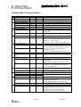
Step-by-Step Testing Procedure
DEVICE NUMBER:
#
Test
1
Voltage Supply
Supply voltage
2
Current consumption
RX mode
TX mode
PD mode
3
Crystal oscillator
Crystal frequency
4
5
6
7
9
10
11
Unit
Condition
V
Measure across device supply pins
mA
mA
uA
at PA output power programmed: ____dBm
Xtal oscillator is (on/off): _____
MHz
Measure approximate frequency using an
oscilloscope.
Measure at peak-to-peak voltage at XOSC_Q1
pin
Oscillator voltage
mVpp
RF frequency
RF frequency
MHz
at RF frequency programmed: ____MHz
Set device to TX mode, NRZ mode, Frequency
separation = 0 Hz. Calibrate.
SA: SPAN=100 kHz, RBW=1 kHz, VBW=Auto
VCO tuning range
VCO min. frequency
MHz
VCO max frequency
MHz
Set device to TX mode. Measure with a
spectrum analyser at antenna output. Configure
the chip to a very low/high frequency as
explained on page 2.
SA: SPAN=200 MHz, RBW=Auto, VBW=Auto
dBc/Hz
SPAN=200 kHz, RBW=1 kHz, VBW=10 Hz
kHz
Measure the distance between the two tops in
the spectrum
SPAN=500 kHz, RBW=3 kHz, VBW=1 kHz
Use Spectrum Analyser FM demodulator option
(frequency versus time). Measure frequency
separation. Make plot.
at PA output power programmed: ____dBm
PA_POW: _____
SPAN=1 MHz, RBW=10 kHz, VBW=1 kHz
Phase noise
Phase noise at 100 kHz
offset
Modulation
Peak to peak deviation
Modulation response
8
Value
kHz
TX output power
Output power
Harmonics
2. harmonic
3. harmonic
LO leakage
Frequency
dBm
LO leakage
Receiver sensitivity
Sensitivity
dBm
SPAN=1 MHz, RBW=10 kHz, VBW=1 kHz
dBm
SWRA073
Shall be 150 kHz above/below the carrier
frequency measured above
SPAN=1 MHz, RBW=10 kHz, VBW=1 kHz
SPAN=1 MHz, RBW=10 kHz, VBW=1 kHz
Use signal generator set up with correct
modulation frequency and deviation.
View DIO and DCLK signal using an
oscilloscope. Adjust level until BER = 10-3
Page 8 of 11
Application Note AN018
Notes to the tests
1. Supply voltage
The supply voltage should be in the range 2.1 – 3.6 V. Operation is not guaranteed outside
this range. If measured voltage is less than expected it could be a current limiter in the power
supply causing the problem.
2. Current consumption
The typical current consumption for the different modes are calculated by SmartRF Studio,
and can be seen in the Status bar of the Normal view. It is also available in the data sheet.
3. Crystal oscillator
The crystal oscillator operation can be verified very simply using an oscilloscope. However,
the actual frequency must be measured when testing the transmitter frequency because the
oscilloscope probe would load the crystal and de-tune it during the test. The peak-to-peak
voltage should be 400 – 600 mVpp.
4. RF frequency
This test measures the accurate RF frequency and hence the crystal frequency. Set the
device to TX mode, NRZ mode and the frequency separation to 0 Hz. Measure with a
spectrum analyser at the antenna output. If the measured frequency is off by a few kHz, then
the load capacitance for the crystal must be changed. If it is far from the expected frequency,
most likely the VCO tuning range is wrong, or calibration has not been done correctly.
5. VCO tuning range
The VCO tuning range is measured by forcing the tuning voltage to min/max by programming
a very low/high frequency. It is important to have a correct (large enough) tuning range in
order to cover the desired frequency for all expected component tolerances. Changing the
VCO inductor value will change the tuning range.
6. Phase noise
The phase noise depends on the loop filter bandwidth, but should typically be –85 dBc/Hz.
When measuring the noise using a spectrum analyser the measurement must be corrected
for the resolution bandwidth. Using 1 kHz resolution bandwidth, the measurement must be
corrected with -30 dBHz (10log(1000)). That means, if you are measuring the noise 100 kHz
away from the carrier to be –55 dBc using 1 kHz resolution bandwidth, the phase noise is (55 – 30) = -85 dBc/Hz at 100 kHz offset.
7. Modulation
Looking at the modulation spectrum can help to discover any problems with the loop
bandwidth. The peak-to-peak deviation should be close to the specified frequency separation.
An excessive deviation could be due to low phase/gain margin in the PLL leading to “peaking”
in the closed loop response. If this is the case, the calibration and the TEST0, TEST2 and
TEST4 registers should be investigated. Looking at the modulation response using an FM
demodulator can also tell a lot about the loop response.
8. TX output power
The output power should be close to the specified output power, but taking the harmonic filter
loss into account. The insertion loss of a low pass LC filter is typically 1.5 – 2 dB. If the output
power is too low, the LC filter should be checked. The filter is very sensitive to layout
paracitics.
9. Harmonics
The transmitter harmonics should be attenuated sufficiently by the LC low-pass filter. Some
spectrum analysers provide automatic measurement of harmonics presenting the result as a
list for convenience.
SWRA073
Page 9 of 11
Application Note AN018
10. LO leakage
The LO leakage is measured at the antenna output when the transceiver is in receive mode.
The LO frequency will be 150 kHz above or below the RF carrier frequency, depending on
whether low-side or high-side LO injection is used (programmable from SmartRF Studio).
11. Sensitivity
Assuming you do not have a Bit Error Tester the sensitivity is measured using a signal
generator with FSK modulation at the specified frequency and deviation. If you do not have
the equipment to send FSK modulation, you can use an RF generator with FM modulation
and use an external function generator to modulate the signal with a square wave (see page
3). The Rx DIO signal and the modulating signal are monitored using an oscilloscope. A bit
error rate (BER) of 10-3 can then be determined visually. The expected sensitivity for different
data rates, frequency separations and current settings are shown in the CC1000 data sheet.
Any loss in the front-end filter must be taken into account.
Less than expected sensitivity can be due to mismatch at the LNA input, excess loss in the
front end filter, or frequency offset between transmitter and receiver.
12. Still problems?
Contact your local distributor (or Chipcon directly) if you still need help on your RF circuit
design. Fill in the test table above as carefully as possible and send to us for further advice.
For more detailed information
Read the information on our web-site. There are several detailed application notes available
as well as a FAQ data base.
General Application Notes:
AN_001_SRD_Regulations
AN_002_LO_emission
AN_007_Manufacturers
AN_021_Voltage_Level_Conversion
CC1000 specific Application Notes:
AN_009_CC1000_MCU_Interfacing
AN_011_Programming_the_CC1000_frequency_for_best_sensitivity
AN_015_RF_Modem_Reference_Design
AN_016_CC1000_CC1050_On_Off_Keying
AN_019_Crystal_Oscillator_Issues_CC1000_CC1010
AN_020_Remote_Keyless_Entry_Reference_Design
SWRA073
Page 10 of 11
Application Note AN018
This application note is written by the staff of Chipcon to the courtesy of our customers.
Chipcon is a world-wide supplier of RFICs. For further information on the products from
Chipcon please contact us or visit our web site. An updated list of distributors is also available
at our web site.
Contact Information
Address:
Chipcon AS
Gaustadalléen 21
N-0349 Oslo,
NORWAY
Telephone
Fax
E-mail
:
:
:
Web site
:
(+47) 22 95 85 44
(+47) 22 95 85 46
[email protected] (information about RF-IC products)
[email protected] (support on our standard products)
http://www.chipcon.com
© Chipcon 2003
Disclaimer
Chipcon AS believes the furnished information is correct and accurate at the time of this printing. However, Chipcon
AS reserves the right to make changes to this application note without notice. Chipcon AS does not assume any
responsibility for the use of the described information. Please refer to Chipcon’s web site for the latest update.
SmartRF® is a registered trademark of Chipcon AS. All other trademarks or registered trademarks are the sole
property of their respective owners.
SWRA073
Page 11 of 11