1
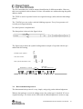
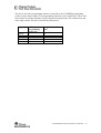
User Manual
CC400DB Demonstration Board
Rev. 2.0
Table of contents
1
INTRODUCTION.....................................................................................................3
2
CC400DB DEMONSTRATION BOARD...............................................................4
2.1
2.2
2.3
2.4
2.5
2.6
3
DEMONSTRATION BOARD SOFTWARE DESCRIPTION.............................9
3.1
3.2
3.3
3.4
3.5
3.6
4
BEFORE STARTING .................................................................................................4
DEMONSTRATOR OPERATION .................................................................................5
SYSTEM PARAMETERS ...........................................................................................5
CONFIGURATION REGISTER DATA ..........................................................................6
MICRO-CONTROLLER EEPROM MAPPING .............................................................7
TROUBLE-SHOOTING..............................................................................................8
SLEEP MODE ..........................................................................................................9
POLLING MODE ......................................................................................................9
DATA PACKET DESCRIPTION ..................................................................................9
DATA TRANSMISSION PROTOCOL .........................................................................10
DATA RECEPTION.................................................................................................11
DATA DECODER ALGORITHM ...............................................................................11
DEMONSTRATION BOARD HARDWARE DESCRIPTION ......................... 12
4.1 RF-SECTION.........................................................................................................12
4.1.1 PLL loop filter..............................................................................................12
4.1.2 IF filter .........................................................................................................12
4.1.3 The modulation input/output........................................................................12
4.1.4 LNA/PA matching ........................................................................................13
4.1.5 Voltage Controlled Oscillator (VCO)..........................................................13
4.1.6 Crystal oscillator .........................................................................................13
4.1.7 Antenna ........................................................................................................13
4.2 CONTROLLER SECTION.........................................................................................14
4.2.1 RC oscillator ................................................................................................14
4.2.2 Micro-controller I/O ....................................................................................14
4.2.3 In-system-programming...............................................................................14
4.3 LAYOUT SKETCHES ..............................................................................................16
4.4 CIRCUIT DIAGRAM ...............................................................................................17
4.5 BILL OF MATERIALS .............................................................................................18
5
USING THE DEMONSTRATOR BOARD AS A PROTOTYPE MODULE... 19
CC400DB Demonstration Board User Manual
2
1
Introduction
The CC400 single chip RF transceiver includes many features and great flexibility,
which makes the chip suitable for a very large number of applications and system
requirements. The CC400DB Demonstration Board is designed to demonstrate how the
CC400 chip can be used in a simple two-way remote control. Full documentation is
provided for this module, including schematic, layout and micro-controller code. This
design will be a starting point and make it very easy for the users to evaluate transceiver
performance, and in a short time develop their own applications based on this reference
design.
The kit includes two CC400DB Demonstration Boards with a complete CC400
transceiver, micro-controller, integrated PCB antenna and battery. The Demonstration
Boards are pre-programmed to serve as a simple demonstrator. By pushing the “ON”
button, the device will be awaked. Both modules should be awaked before a
transmission takes place. A transmission is initiated by pushing the “TX” button. A
blinking sequence of approximately one-second duration is then transmitted and shown
on the receivers LED. The same “message” is returned from the receiver to the initial
transmitter and shown on its LED as an “acknowledge”. The modules will enter sleep
mode after being left without operation for one minute.
Technical features:
0dBm RF power
Up to150 meter range (depending on antenna orientation)
Small integrated shorted-stub antenna
<1uA power-down current in sleep mode
3.6V Lithium battery supply (~1000mAh)
From SmartRF® Studio it is possible to reconfigure the CC400DB system parameters by
inserting the Demonstration Board into the CC400EB Evaluation Board edge connector.
It is also possible to upgrade the Demonstration Board with new micro-controller
program code from SmartRF® Studio.
The CC400DB is also designed to work together with the Atmel AVR micro-controller
STK500 development board, the in-system programmer ATAVRISP or similar. At the
rear side of the board there is a 10 pin connector foot-print which fits a 10-pin ISP cable.
This user manual describes how to use the Demonstration Board and how to develop
new applications. You will also find a detailed description of the circuit board and the
micro-controller code.
All available documentation can be downloaded from our web site. That includes:
CC400DB User Manual (this document)
CC400DB micro-controller code and configuration data
CC400 data sheet
CC400DB Demonstration Board User Manual
3
2
2.1
CC400DB Demonstration Board
Before starting
The CC400DB runs on a 3.6V Lithium battery. If the battery is not mounted and
soldered to the board, insert the battery at the rear side of the board. Observe the LED. If
the LED is turned on continuously, push the “ON” button. For proper operation the LED
shall be pulsing with a period of approximately one second. If not, remove the battery
momentarily and reconnect. The battery terminals should be soldered for proper
operation.
Important: Be sure not to short-circuit the battery terminals during soldering or at any
point of use.
Before using the CC400DB: The use of radio transceivers is regulated by international
and national rules. Before transmitting a RF signal, please contact your local
telecommunication authorities to check if you are licensed to operate the transceiver.
CC400DB Demonstration Board User Manual
4
2.2
Demonstrator operation
The CC400DB demonstrates a very simple two-way remote control system.
To “wake” the module from power-down mode, simply press the “ON” button for a
short time. The LED will then start blinking with a period of approximately 1 second.
This is the “heart-beat” that shows the module is operating. During the short time the
LED is lit, the module is in active receive mode, and listens for a data packet. If a data
packet is not found, it goes to a “rest” mode for approximately 1 second. Hence, the
module listens for a data packet every second. This polled receiver algorithm is
implemented in order to save battery power.
Both modules should be awaked before a successful transmission can take place. A
transmission is initiated by pushing the “TX” button. A data packet of approximately 1.5
second duration is then transmitted. The data packet consists of a long preamble and a
short data field. The pre-amble is longer than 1 second to ensure that the transmission
intercepts with the polled receiver.
The data packet transmitted consists of a blinking sequence of approximately 2 seconds
duration, and will be shown on the receiver’s LED if the data packet was received free
of errors. The same “message” with an acknowledgement flag is then returned from the
receiver to the initial transmitter. Again, the blinking sequence will be shown on the
LED as a receipt acknowledge.
The modules will enter sleep mode after being left without operation for about one
minute. The CC400 and the micro-controller are then in power-down mode, ensuring
minimum power consumption.
The timing diagram below illustrates a packet transmission sequence when the
transmission is initiated from device number 2.
Receiver polling
Initial
transmission
DEVICE 1
DEVICE 2
2.3
RX
Message
shown on
receiver LED
LED
TX
Ack.
transmission
Acknowledge
shown on
receiver LED
Devices are active for one
minute until time-out
Sleep
mode
TX ACK
RX
LED (ACK)
System parameters
The system parameters used to generate the configuration data for the CC400DB is
shown below. This is a printout from the SmartRF® Studio software.
System parameters:
X-tal frequency: 12.000000 MHz
X-tal accuracy: +/- 50 ppm
CC400DB Demonstration Board User Manual
5
RF frequency: 433.920 MHz
IF stage: 200 kHz
Frequency separation: 40 kHz
Data rate: 1.2 kbps
Power amplifier class: Class B
RF output power: 0 dBm
Mode: TX
Receiver mode: Optimum sensitivity
LOCK indicator: Continuous
2.4
Configuration register data
Based on the system parameters referred above, the following configuration data is
generated. This is a printout from the SmartRF® Studio software.
RX mode:
Frame Addr/Data (hex)
A
002A
B
330B
C
4041
D
7EE1
E
8A00
F
BA02
G
CB6C
H
E040
TX mode:
Frame Addr/Data (hex)
A
082A
B
330B
C
4041
D
7F9A
E
8A29
F
BA02
G
CB6C
H
E040
PD osc. on mode:
Frame Addr/Data (hex)
A
182A
B
330B
C
4041
D
7EE1
E
8A00
F
BA02
G
CB6C
H
E040
CC400DB Demonstration Board User Manual
6
PD osc. off mode:
Frame Addr/Data (hex)
A
182A
B
330B
C
4051
D
7EE1
E
8A00
F
BA02
G
CB6C
H
E040
RX Precharge mode:
Frame Addr/Data (hex)
A
002A
B
330B
C
4041
D
7EE1
E
8A00
F
BA02
G
CB6C
H
E248
In this application we have decided to use RX precharge, RX, TX and PD osc. off
modes. Shown in bold in the listing above is the configuration data that is used, and
stored in the micro-controller EEPROM.
Note: The frame address is combined with the data to get a two-byte word consisting of
3 address bits (as MSBs) and the 13 data bits (as LSBs). The combined value is shown
in these listings.
2.5
Micro-controller EEPROM mapping
The CC400 configuration data are stored in the micro-controller EEPROM. The
following map shows the data location. To customise the module for a different
frequency or power level, the EEPROM data can be replaced by new values found using
the SmartRF® Studio software.
EEPROM
Address (hex)
00
02
04
06
08
0A
0C
0E
10
12
Data (hex)
Reference
082A
330B
4041
7F9A
8A29
BA02
CB6C
E040
E040
002A
TX frame A
TX frame B
TX frame C
TX frame D
TX frame E
TX frame F
TX frame G
TX frame H
RX frame H
RX PC frame A
Comment
CC400DB Demonstration Board User Manual
7
14
16
18
1A
1C
1E
20
22
330B
4041
7EE1
8A00
BA02
CB6C
E248
182A
24
4051
2.6
RX PC frame B
RX PC frame C
RX PC frame D
RX PC frame E
RX PC frame F
RX PC frame G
RX PC frame H
PD (osc. Off) frame
A
PD (osc. Off) frame
C
Trouble-shooting
If the module do not operate as described in this document, try the following.
Problem
LED is continuously on
LED does not start blinking after “ON” is
pressed
Receiver does not receive packet from
closely located transmitter.
Possible solution
Push the “ON” button once more. If this
does not work, reset the micro-controller
(see below).
Check battery voltage. If less than 2.7 Volt,
replace battery. Only replace with a battery
of the same type.
If battery voltage is OK, reset the microcontroller (see below).
Use a Spectrum Analyser at 433.92 MHz to
check the module during transmission.
Connect the analyser to the external antenna
connector foot-print and measure the output
power and frequency using the “max hold”
function. The output power shall be
approximately 0dBm (1mW) with a peak at
433.92MHz +/-10kHz.
Test the receiver the same way in transmit
mode.
The micro-controller can be reset by shorting the reset line to ground for a short
moment. The reset line is located at the edge connector pin 6. Ground is pin 1. The
orientation mark is between pin 2 and 3.
CC400DB Demonstration Board User Manual
8
3
Demonstration Board software description
The demonstration board software is implemented in assembly and runs on the Atmel
AVR 8-bit micro-controller ATtiny12L.
The micro-controller handles the CC400 configuration, data encoding and decoding
using Manchester code, and implements a simple packet protocol.
A program listing with the assembly source code is available for reference and can be
used as a starting point for your own applications using the AVR series of controllers
from Atmel.
3.1
Sleep mode
When the CC400DB is left inactive for approximately one minute the CC400 is set to
power down mode, and the controller goes to “sleep”. The controller is awaked by an
interrupt signal at INT0 (pin 6).
In sleep mode the current consumption is less than 1 µA.
3.2
Polling mode
In polling mode the CC400 is used for receive polling. Once every second the CC400 is
set to RX mode, and the micro-controller starts searching for a preamble. The microcontroller reads two data bits, if these are not Manchester coded 1’s, the CC400 is set to
power down mode again. The LED is lit during the pre-amble search and will appear as
a “heartbeat” signal.
In polling mode the “TX” button input (PB2) is also monitored. If this line is pulled low
by the push button, the micro-controller will configure the CC400 to TX mode, and send
a predefined data packet at the DIO line (PB1), before returning to receiver polling.
3.3
Data packet description
The data packet consists of a pre-amble, a start-of-frame (SOF), and a data field.
The pre-amble is a train of ‘1’s. The train is longer than 1 second in order to ensure that
it intercept with a polled receiver.
The SOF consists of two consecutive ‘0’s. The SOF marks the end of the preamble, and
the start of the actual data.
The data field consists of ID (identification), TYPE (packet type) and DATA (user data,
3 bytes). No FEC (forward error correction) or CRC (cyclic redundancy check) is used
in order to keep it as simple as possible.
CC400DB Demonstration Board User Manual
9
The ID is intended to be used for unique identification of different modules. However,
this is not exploited in this software revision. All modules are addressed using the public
address (0x00).
The TYPE is used to separate between an original message (0x80) and an acknowledge
(0x81).
The 3 DATA bytes are used to code the blinking sequence. Every bit represents a 0.1
seconds period approximately.
No end of packet is implemented.
The data packet is shown in the figure below.
Preamble
SOF
ID
TYPE DATA1 DATA2 DATA3
The figure below shows the symbol coding and an example of a packet with the preamble and SOF timing.
Preamble (synch symbol):
SOF, start of frame:
Data symbols (Manchester code):
Preamble for >1 second
3.4
1=
SOF
0=
Data field:
ID, TYPE, DATA1,2,3
Data transmission protocol
The data transmission protocol is very simple, using only packet acknowledgement.
When a data package is received without errors, the packet type is checked. If it is an
original message, it is shown on the LED, and an acknowledgement is sent as a reply.
CC400DB Demonstration Board User Manual
10
However, if it is an acknowledgement packet that is received, the message is only shown
on the LED without any reply.
3.5
Data reception
The data reception algorithm is as follows:
1. Enter RX precharge mode, wait
2. Enter RX mode
3. The receiver shall receive synchronisation pattern (pre-amble) for some periods
before it is allowed to detect SOF
4. Wait for SOF
5. Receive and decode data
6. Display data on LED
3.6
Data decoder algorithm
The decoder algorithm implemented is based on oversampling. Each bit is sampled 8
times, and the data decision is based on a majority vote. The use of oversampling makes
the data decision more immune to noise and duty cycle variations than a data decision
algorithm based entirely on detecting edges.
The oversampling algorithm synchronises on the preamble, and thereafter continues to
synchronise itself by detecting edges.
For more information on oversampling, see application note AN008 : Oversampling and
data decision.
CC400DB Demonstration Board User Manual
11
4
4.1
Demonstration Board hardware description
RF-section
The RF section consists of a CC400 chip with a few external components. The different
parts of the circuit are explained below.
4.1.1 PLL loop filter
The PLL loop filter contains the components C121-C123 and R121-R123. The
SmartRF® Studio software program has been used to calculate the component values.
Using the calculated component values for the loop filter gives an optimum loop
bandwidth for the selected system parameters.
The transmitted frequency is FSK modulated, which means that the bits ‘0’ and ‘1’ is
coded by jumping between two different frequencies. The loop filter bandwidth is
optimised according to the frequency separation (difference between the two
frequencies) and the data rate (the speed we jump between these two frequencies).
4.1.2 IF filter
The Demonstration Board use the internal 200kHz IF filter. The 200kHz IF filter has a
larger bandwidth than the 60 kHz IF filter, and therefor allows us to use a less accurate,
and hence less expensive crystal. The sensitivity is slightly less than for the 60 kHz IF,
but is considered adequate in this application.
4.1.3 The modulation input/output
The modulation input/output (DIO) is connected to a micro-controller I/O pin. The data
to be sent is Manchester encoded (also known as bi-phase-level coding) by the microcontroller. The Manchester code ensures that the signal has no DC component, which is
necessary for the FSK demodulator to work in an optimal way. The Manchester code is
based on transitions; a “0” is encoded as a low-to-high transition, a “1” is encoded as a
high-to-low transition. This is illustrated in the figure below.
10110001101
TX
data
Time
CC400DB Demonstration Board User Manual
12
4.1.4 LNA/PA matching
The input/output antenna matching network is optimised for 433.92MHz operation. The
component values were calculated in the SmartRF® Studio software program, and
consist of C51, C61, L51 and L61. To compensate for layout parasitics the component
values were tuned to optimise for 50 Ohm input impedance in receive mode, and
maximum output power in transmit mode.
4.1.5 Voltage Controlled Oscillator (VCO)
The VCO tank is optimised for the 433MHz band, covering approximately 410 –
450MHz. The tank contains the components C91, C92, C93, L91 and the variable
capacitance D2.
4.1.6 Crystal oscillator
The crystal oscillator frequency is 12.000 MHz set by X1. We have chosen a low cost
crystal for this application. The crystal is specified as 50/50/10/12, which means that it
has a +/- 50ppm initial tolerance, and will drift less than +/-50ppm over a temperature
range of –10 to 60°C. SmartRF® Studio specifies a total crystal accuracy of +/-50ppm
for the parameters used here. This means that the total system is only specified for room
temperature, as all the accuracy is “used up” for the initial tolerance. If a wider
temperature range is required, a higher accuracy crystal should be used.
The loading capacitors, C151 and C161, together with the input capacitance and
paracitics makes up the total 12pF load capacitance the crystal is designed for.
4.1.7 Antenna
This antenna is an example of a PCB integrated antenna. Several antenna configurations
were evaluated, and the short stub was found to be the best solution for this application.
As the stub is shorter than one-quarter wavelength (λ/4 = 16.4 cm at 433.92MHz), it has
to be prolonged and matched using lumped elements. The short stub has a capacitive
reactance and is thus prolonged using an inductor (L8) in series. Another inductor in
shunt (L7) matches the antenna to 50 Ohm.
The antenna is fairly omni-directional, but have slightly more emission sideways. This
follows from the fact that the antenna elements and the ground plane have the largest
physical dimensions normal to this direction. Placing the board in a vertical direction, or
placing two units parallel sideways will give the best range.
In general, small electrical antennas are not very efficient. Electrical stub antennas
should be designed as long as possible, up to one-quarter wavelength. They should be
kept away from the ground plane and other surrounding metallic bodies. For hand-held
remote controls, the antenna should not be in close contact with the hand. If this can not
CC400DB Demonstration Board User Manual
13
be avoided, a magnet loop antenna could be used. The loop is less sensitive to nearby
objects, but suffers of very low efficiency due to very low radiation resistance. The stub
antenna implemented at the Demonstrator PCB showed better efficiency than a loop of
similar size, even when operated hand-held.
4.2
Controller section
The controller section consists of an Atmel AVR ATtiny12L micro-controller with a few
external components.
4.2.1 RC oscillator
The internal RC oscillator is used as reference time base. The oscillator frequency is
relatively independent of temperature and operating voltage. Its nominal frequency is 1.2
MHz, varying less than +/- 5% over the application temperature and supply voltage
range. A calibration feature utilising a calibration word programmed into the microcontroller at the factory ensures that the oscillator frequency is equal from unit to unit.
4.2.2 Micro-controller I/O
As the controller is packed in an 8-pin package, it has room for only 5 external I/O lines.
These are combined serving several functions in different operating modes.
The micro-controller has only one interrupt input, PB1/INT0. This input is shared
between the “ON” button and the DIO signal to CC400. In sleep mode the controller
will be awaked by an interrupt when this line is forced low by the push button. In
receive mode the interrupt is used for data decoding. During transmit the pin is
configured as an output.
The table below shows the function of all I/O pins in the various modes.
Signal/pin
PB0, pin 5
PB1/INT0,
pin 6
PB2, pin 7
Program
loading
MOSI
MISO
SCK
PB3, pin 2
PB4, pin 3
Demonstrator
LED
DIO
“ON” in sleep mode
CLOCK
“TX”
STROBE
PDATA
Comment
Interrupt input
4.2.3 In-system-programming
Using the ATMEL AVR STK500 development board, ATAVRISP in-circuit
programmer or similar devices, the micro-controller can be reprogrammed while in the
circuit. Both the program code memory (flash) and the EEPROM can be reprogrammed.
CC400DB Demonstration Board User Manual
14
The device used for programming must be connected to the CC400DB programming
socket or edge finger contact. The programming interface uses 4 signal lines. These four
lines can be accessed at both the 10-pin connector footprint at the rear of the board, and
at the edge contact. Pin-out is listed in the table below.
Signal/pin AVR
programming
socket, pin
MOSI
1
MISO
9
SCK
7
RESET
5
GROUND 4,6,8,10
Edge connector,
pin
4
5
3
6
1,2
CC400DB Demonstration Board User Manual
15
4.3
Layout sketches
CC400DB Demonstration Board User Manual
16
4.4
Circuit diagram
CC400DB Demonstration Board User Manual
17
4.5
Bill of materials
Reference
B1
Description
Battery
C1
C2
C3
C10
C11
C12
C24
C25
C51
C52
C53
C61
C91
C92
C93
C121
C122
C123
C151
C161
C210
C211
D1
D2
L7
L8
L51
L52
L61
L91
L210
R1
R2
R3
R4
R5
R6
R7
R121
R122
R123
S1
S2
U1
U2
X1
Capacitor, tantal
Capacitor 0603
Capacitor 0603
Capacitor 0603
Capacitor 0603
Capacitor 1206
Capacitor 0603
Capacitor 0603
Capacitor 0603
Capacitor 0603
Capacitor 0603
Capacitor 0603
Capacitor 0603
Capacitor 0603
Capacitor 0603
Capacitor 0603
Capacitor 0603
Capacitor 0603
Capacitor 0603
Capacitor 0603
Capacitor 0603
Capacitor 0603
LED
Varactor diode
Inductor 0805
Inductor 0805
Inductor 0805
Inductor 0805
Inductor 0805
Inductor 0805
EMI filter bead
Resistor 0603
Resistor 0603
Resistor 0603
Resistor 0603
Resistor 0603
Resistor 0603
Resistor 0603
Resistor 0603
Resistor 0603
Resistor 0603
Push button
Push button
Single chip transceiver
Micro-controller
Crystal, HC-49-SMD
CC400DB
Value
3.6V
3.3µF
33nF
220pF
1nF
33nF
4.7nF
33pF
220pF
220pF
15pF
22pF
12pF
4.7pF
8.2pF
3.9pF
33nF
1.5nF
330pF
15pF
15pF
1nF
33nF
Red
18nH
56nH
39nH
8.2nH
6.8nH
10nH
10kΩ
1kΩ
1kΩ
0Ω
1kΩ
470Ω
10kΩ
5.6kΩ
27kΩ
22kΩ
Part
LS14250 3PF, Lithium Thionyl
Cloride
C_3U3_TAN_B
C_33N_0603_X7R_K_25
C_220P_0603_NP0_G_50
C_1N0_0603_X7R_K_50
C_33N_0603_X7R_K_25
C_4N7_1206_NP0_J_50
C_33P_0603_NP0_J_50
C_220P_0603_NP0_G_50
C_220P_0603_NP0_G_50
C_15P_0603_NP0_G_50
C_22P_0603_NP0_J_50
C_12P_0603_NP0_G_50
C_4P7_0603_NP0_C_50
C_8P2_0603_NP0_C_50
C_3P9_0603_NP0_C_50
C_33N_0603_X7R_K_25
C_1N5_0603_X7R_K_50
C_330P_0603_NP0_J_50
C_15P_0603_NP0_G_50
C_15P_0603_NP0_G_50
C_1N0_0603_X7R_K_50
C_33N_0603_X7R_K_25
CL150, Citizen
KV1832C, Toko
L_18N_0805_J
L_56N_0805_J
L_39N_0805_J
L_8N2_0805_J
L_6N8_0805_J
L_10N_0805_J, Murata LQN21A
BLM11A102S, Murata
R_10K_0603_G
R_1K0_0603_J
R_1K0_0603_J
R_0R_0603
R_1K0_0603_J
R_470_0603_J
R_10K_0603_G
R_5K6_0603_G
R_27K_0603_J
R_22K_0603_G
PUSH BUTTON
PUSH BUTTON
CC400
ATtiny12L-4SC
X_12.000000 MHz, 12pF load
CC400DB Demonstration Board User Manual
18
5
Using the Demonstrator Board as a prototype module
The purpose of the Demonstrator Board is to show a simple transceiver module with
battery supply and integrated PCB antenna. The demonstrator can be used “as is” for
simple range and coverage measurements. But keep in mind that this module uses only 0
dBm and a small rather ineffective antenna. The range can be extended substantially
using more power and a better antenna.
The Demonstrator Board can also be used as a prototype module when developing your
own applications. You may:
•
•
•
•
Reprogram the EEPROM configuration data for your own system parameters.
SmartRF® Studio generates the configuration data values. See section 2.5 for
EEPROM memory map.
Rewrite the micro-controller code to use the edge connector to interface your host
system
Insert a standard 2.54mm pitch contact to interface a motherboard at the edge
connector.
Remove L7 and L8, and mount a coax connector at the antenna output. Thus an
external antenna could be used. The antenna should be matched to 50 Ohm
CC400DB Demonstration Board User Manual
19