1
Order this document by
MC68EZ328UM/D
(Motorola Order Number)
Rev. 1, 11/98
MC68EZ328
Integrated Processor
UserÕs Manual
Motorola, Incorporated
Semiconductor Products Sector
6501 William Cannon Drive West
Austin TX 78735-8598
©MOTOROLA INC., 1998. All rights reserved.
This document contains information on a new product. Specifications and information herein are subject to change
without notice.
Motorola reserves the right to make changes without further notice to any products herein to improve
reliability, function, or design. Motorola does not assume any liability arising out of the application or use
of any product or circuit described herein; neither does it convey any license under its patent rights nor the
rights of others. Motorola products are not designed, intended, or authorized for use as components in
systems intended for surgical implant into the body, or other application in which the failure of the
Motorola product could create a situation where personal injury or death may occur. Should Buyer
purchase or use Motorola products for any such unintended or unauthorized application, Buyer shall
indemnify and hold Motorola and its officers, employees, subsidiaries, affiliates, and distributors harmless
against all claims, costs, damages, and expenses, and reasonable attorney fees arising out of, directly or
indirectly, any claim of personal injury or death associated with such unintended or unauthorized use,
even if such claim alleges that Motorola was negligent regarding the design or manufacture of the part.
are registered trademarks of Motorola, Inc. Motorola, Inc. is an Equal
Motorola and
Opportunity/Affirmative Action Employer
OnCE and Mfax are trademarks of Motorola, Inc.
TABLE OF CONTENTS
Paragraph
Number
Title
Page
Number
PREFACE
Related Documentation. . . . . . . . . . . . . . . . . . . . . . . . . . . . . . . . . . . . . . . . . . . . . . xvii
Organization of This Manual . . . . . . . . . . . . . . . . . . . . . . . . . . . . . . . . . . . . . . . . . . xvii
SECTION 1
BASIC ARCHITECTURE
1.1
1.1.1
1.1.2
1.1.3
1.2
1.3
1.4
1.5
1.6
1.7
1.8
1.9
1.10
1.11
1.12
1.13
1.14
1.15
Core . . . . . . . . . . . . . . . . . . . . . . . . . . . . . . . . . . . . . . . . . . . . . . . . . . . . . . . 1-2
Core Programming Model . . . . . . . . . . . . . . . . . . . . . . . . . . . . . . . . . . . . 1-2
Data and Address Mode Types. . . . . . . . . . . . . . . . . . . . . . . . . . . . . . . . 1-4
EC000 Instruction Set . . . . . . . . . . . . . . . . . . . . . . . . . . . . . . . . . . . . . . . 1-5
Chip-Select Logic and Bus Interface . . . . . . . . . . . . . . . . . . . . . . . . . . . . . . 1-6
Phase-Locked Loop and Power Control. . . . . . . . . . . . . . . . . . . . . . . . . . . . 1-6
Interrupt Controller . . . . . . . . . . . . . . . . . . . . . . . . . . . . . . . . . . . . . . . . . . . . 1-7
Parallel General-Purpose I/O Ports . . . . . . . . . . . . . . . . . . . . . . . . . . . . . . . 1-7
Pulse-Width Modulator . . . . . . . . . . . . . . . . . . . . . . . . . . . . . . . . . . . . . . . . . 1-7
General-Purpose Timer . . . . . . . . . . . . . . . . . . . . . . . . . . . . . . . . . . . . . . . . 1-7
Serial Peripheral Interface . . . . . . . . . . . . . . . . . . . . . . . . . . . . . . . . . . . . . . 1-7
UART and Infra-Red Communication Support . . . . . . . . . . . . . . . . . . . . . . . 1-8
LCD Controller . . . . . . . . . . . . . . . . . . . . . . . . . . . . . . . . . . . . . . . . . . . . . . . 1-8
Real-Time Clock . . . . . . . . . . . . . . . . . . . . . . . . . . . . . . . . . . . . . . . . . . . . . . 1-8
DRAM Controller . . . . . . . . . . . . . . . . . . . . . . . . . . . . . . . . . . . . . . . . . . . . . 1-8
In-Circuit Emulation Module . . . . . . . . . . . . . . . . . . . . . . . . . . . . . . . . . . . . . 1-8
Bootstrap Mode . . . . . . . . . . . . . . . . . . . . . . . . . . . . . . . . . . . . . . . . . . . . . . 1-8
Memory Map. . . . . . . . . . . . . . . . . . . . . . . . . . . . . . . . . . . . . . . . . . . . . . . . . 1-8
SECTION 2
SIGNAL DESCRIPTIONS
2.1
2.2
2.3
2.4
2.5
2.6
2.7
2.8
Signals GROUped by Function . . . . . . . . . . . . . . . . . . . . . . . . . . . . . . . . . . 2-3
POWER and Ground Signals . . . . . . . . . . . . . . . . . . . . . . . . . . . . . . . . . . . . 2-4
CLOCK and System Control Signals . . . . . . . . . . . . . . . . . . . . . . . . . . . . . . 2-4
ADDRESS BUS Signals . . . . . . . . . . . . . . . . . . . . . . . . . . . . . . . . . . . . . . . . 2-5
DATA BUS Signals. . . . . . . . . . . . . . . . . . . . . . . . . . . . . . . . . . . . . . . . . . . . 2-5
BUS CONTROL Signals. . . . . . . . . . . . . . . . . . . . . . . . . . . . . . . . . . . . . . . . 2-6
INTERRUPT CONTROLler Signals . . . . . . . . . . . . . . . . . . . . . . . . . . . . . . . 2-6
LCD CONTROLLER Signals . . . . . . . . . . . . . . . . . . . . . . . . . . . . . . . . . . . . 2-7
MOTOROLA
MC68EZ328 USERÕS MANUAL
v
2.9
2.10
2.11
2.12
2.13
2.14
UART Controller Signals . . . . . . . . . . . . . . . . . . . . . . . . . . . . . . . . . . . . . . . 2-8
TIMER Signal . . . . . . . . . . . . . . . . . . . . . . . . . . . . . . . . . . . . . . . . . . . . . . . . 2-8
Pulse-Width Modulator Signal . . . . . . . . . . . . . . . . . . . . . . . . . . . . . . . . . . . 2-8
Serial Peripheral Interface Signals . . . . . . . . . . . . . . . . . . . . . . . . . . . . . . . . 2-8
CHIP-SELECT Signals. . . . . . . . . . . . . . . . . . . . . . . . . . . . . . . . . . . . . . . . . 2-9
In-Circuit EMULATion Signals . . . . . . . . . . . . . . . . . . . . . . . . . . . . . . . . . . . 2-9
SECTION 3
SYSTEM CONTROL
3.1
3.2
Operation . . . . . . . . . . . . . . . . . . . . . . . . . . . . . . . . . . . . . . . . . . . . . . . . . . . 3-1
Programming Model . . . . . . . . . . . . . . . . . . . . . . . . . . . . . . . . . . . . . . . . . . . 3-2
3.2.1
System Control Register . . . . . . . . . . . . . . . . . . . . . . . . . . . . . . . . . . . . . 3-2
SECTION 4
CHIP-SELECT LOGIC
4.1
4.1.1
4.1.2
4.1.3
4.2
4.2.1
4.2.2
4.2.3
4.3
Chip-Select Operation . . . . . . . . . . . . . . . . . . . . . . . . . . . . . . . . . . . . . . . . . 4-2
Memory Protection . . . . . . . . . . . . . . . . . . . . . . . . . . . . . . . . . . . . . . . . . 4-2
Programmable Data Bus Size. . . . . . . . . . . . . . . . . . . . . . . . . . . . . . . . . 4-3
Overlapping Chip-Select Registers. . . . . . . . . . . . . . . . . . . . . . . . . . . . . 4-4
PROGRAMMING MODEL . . . . . . . . . . . . . . . . . . . . . . . . . . . . . . . . . . . . . . 4-4
Chip-Select Group Base Address Registers. . . . . . . . . . . . . . . . . . . . . . 4-4
Chip-Select Registers . . . . . . . . . . . . . . . . . . . . . . . . . . . . . . . . . . . . . . . 4-5
Emulation Chip-Select Register . . . . . . . . . . . . . . . . . . . . . . . . . . . . . . . 4-8
Programming Example. . . . . . . . . . . . . . . . . . . . . . . . . . . . . . . . . . . . . . . . . 4-9
SECTION 5
PHASE-LOCKED LOOP AND POWER CONTROL
5.1
5.1.1
5.1.2
5.1.3
5.1.4
5.1.5
5.2
5.2.1
5.2.2
5.3
5.3.1
5.3.2
Operation . . . . . . . . . . . . . . . . . . . . . . . . . . . . . . . . . . . . . . . . . . . . . . . . . . . 5-2
Using the PLL To Reduce Power Consumption . . . . . . . . . . . . . . . . . . . 5-2
PLL Operation at Power-Up . . . . . . . . . . . . . . . . . . . . . . . . . . . . . . . . . . 5-2
PLL Operation at Wake-Up. . . . . . . . . . . . . . . . . . . . . . . . . . . . . . . . . . . 5-2
Changing the VCO Frequency . . . . . . . . . . . . . . . . . . . . . . . . . . . . . . . . 5-3
PLL Operation at System Shut-Down . . . . . . . . . . . . . . . . . . . . . . . . . . 5-3
Programming Model . . . . . . . . . . . . . . . . . . . . . . . . . . . . . . . . . . . . . . . . . . . 5-4
PLL Control Register. . . . . . . . . . . . . . . . . . . . . . . . . . . . . . . . . . . . . . . . 5-4
PLL Frequency Select Register . . . . . . . . . . . . . . . . . . . . . . . . . . . . . . . 5-5
POWER CONTROL . . . . . . . . . . . . . . . . . . . . . . . . . . . . . . . . . . . . . . . . . . . 5-6
Operating the Power Control Module . . . . . . . . . . . . . . . . . . . . . . . . . . . 5-8
Power Control Register. . . . . . . . . . . . . . . . . . . . . . . . . . . . . . . . . . . . . . 5-9
SECTION 6
INTERRUPT CONTROLLER
vi
MC68EZ328 USERÕS MANUAL
MOTOROLA
6.1
6.2
6.3
6.3.1
6.4
6.5
6.6
6.6.1
6.6.2
6.6.3
6.6.4
6.6.5
6.7
6.8
Interrupt Processing . . . . . . . . . . . . . . . . . . . . . . . . . . . . . . . . . . . . . . . . . . . 6-1
Exception Vectors. . . . . . . . . . . . . . . . . . . . . . . . . . . . . . . . . . . . . . . . . . . . . 6-3
Reset . . . . . . . . . . . . . . . . . . . . . . . . . . . . . . . . . . . . . . . . . . . . . . . . . . . . . . 6-4
DATA BUS WIDTH FOR BOOT DEVICE OPERATION . . . . . . . . . . . . . 6-5
INTERRUPT CONTROLLER operation . . . . . . . . . . . . . . . . . . . . . . . . . . . . 6-5
Vector Generator . . . . . . . . . . . . . . . . . . . . . . . . . . . . . . . . . . . . . . . . . . . . . 6-6
Programming Model . . . . . . . . . . . . . . . . . . . . . . . . . . . . . . . . . . . . . . . . . . . 6-6
Interrupt Vector Register . . . . . . . . . . . . . . . . . . . . . . . . . . . . . . . . . . . . . 6-6
Interrupt Control Register . . . . . . . . . . . . . . . . . . . . . . . . . . . . . . . . . . . . 6-7
Interrupt Mask Register. . . . . . . . . . . . . . . . . . . . . . . . . . . . . . . . . . . . . . 6-9
Interrupt Status Register . . . . . . . . . . . . . . . . . . . . . . . . . . . . . . . . . . . . 6-11
Interrupt Pending Register . . . . . . . . . . . . . . . . . . . . . . . . . . . . . . . . . . 6-16
KEYBOARD INTERRUPTs . . . . . . . . . . . . . . . . . . . . . . . . . . . . . . . . . . . . 6-20
PEN Interrupts . . . . . . . . . . . . . . . . . . . . . . . . . . . . . . . . . . . . . . . . . . . . . . 6-20
SECTION 7
PARALLEL PORTS
7.1
7.2
7.2.1
7.2.2
7.2.3
7.2.4
7.2.5
7.2.6
7.2.7
Operation . . . . . . . . . . . . . . . . . . . . . . . . . . . . . . . . . . . . . . . . . . . . . . . . . . . 7-1
Programming Model . . . . . . . . . . . . . . . . . . . . . . . . . . . . . . . . . . . . . . . . . . . 7-2
Port A Registers . . . . . . . . . . . . . . . . . . . . . . . . . . . . . . . . . . . . . . . . . . . 7-2
Port B Registers . . . . . . . . . . . . . . . . . . . . . . . . . . . . . . . . . . . . . . . . . . . 7-3
Port C Registers . . . . . . . . . . . . . . . . . . . . . . . . . . . . . . . . . . . . . . . . . . . 7-5
Port D Registers . . . . . . . . . . . . . . . . . . . . . . . . . . . . . . . . . . . . . . . . . . . 7-7
Port E Registers . . . . . . . . . . . . . . . . . . . . . . . . . . . . . . . . . . . . . . . . . . 7-10
Port F Registers . . . . . . . . . . . . . . . . . . . . . . . . . . . . . . . . . . . . . . . . . . 7-12
Port G Registers . . . . . . . . . . . . . . . . . . . . . . . . . . . . . . . . . . . . . . . . . . 7-14
SECTION 8
PULSE-WIDTH MODULATOR
8.1
8.1.1
8.1.2
8.1.3
8.2
8.2.1
8.2.2
8.2.3
8.2.4
8.3
Operation . . . . . . . . . . . . . . . . . . . . . . . . . . . . . . . . . . . . . . . . . . . . . . . . . . . 8-1
Playback Mode . . . . . . . . . . . . . . . . . . . . . . . . . . . . . . . . . . . . . . . . . . . . 8-1
Tone Mode . . . . . . . . . . . . . . . . . . . . . . . . . . . . . . . . . . . . . . . . . . . . . . . 8-2
D/A Mode . . . . . . . . . . . . . . . . . . . . . . . . . . . . . . . . . . . . . . . . . . . . . . . . 8-2
Programming Model . . . . . . . . . . . . . . . . . . . . . . . . . . . . . . . . . . . . . . . . . . . 8-2
PWM Control Register . . . . . . . . . . . . . . . . . . . . . . . . . . . . . . . . . . . . . . 8-2
PWM Sample Register . . . . . . . . . . . . . . . . . . . . . . . . . . . . . . . . . . . . . . 8-5
PWM Period Register . . . . . . . . . . . . . . . . . . . . . . . . . . . . . . . . . . . . . . . 8-5
PWM Counter Register . . . . . . . . . . . . . . . . . . . . . . . . . . . . . . . . . . . . . . 8-6
Programming Example . . . . . . . . . . . . . . . . . . . . . . . . . . . . . . . . . . . . . . . . . 8-6
SECTION 9
GENERAL-PURPOSE TIMER
9.1
OPERATION . . . . . . . . . . . . . . . . . . . . . . . . . . . . . . . . . . . . . . . . . . . . . . . . 9-1
MOTOROLA
MC68EZ328 USERÕS MANUAL
vii
9.2
9.2.1
9.2.2
9.2.3
9.2.4
9.2.5
9.2.6
Programming Model . . . . . . . . . . . . . . . . . . . . . . . . . . . . . . . . . . . . . . . . . . . 9-2
Timer Control Register . . . . . . . . . . . . . . . . . . . . . . . . . . . . . . . . . . . . . . 9-2
Timer Prescaler Register . . . . . . . . . . . . . . . . . . . . . . . . . . . . . . . . . . . . 9-4
Timer Compare Register. . . . . . . . . . . . . . . . . . . . . . . . . . . . . . . . . . . . . 9-4
Timer Capture Register. . . . . . . . . . . . . . . . . . . . . . . . . . . . . . . . . . . . . . 9-4
Timer Counter Register. . . . . . . . . . . . . . . . . . . . . . . . . . . . . . . . . . . . . . 9-5
Timer Status Register . . . . . . . . . . . . . . . . . . . . . . . . . . . . . . . . . . . . . . . 9-5
SECTION 10
SERIAL PERIPHERAL INTERFACE MASTER
10.1
OPERATION . . . . . . . . . . . . . . . . . . . . . . . . . . . . . . . . . . . . . . . . . . . . . . . 10-1
10.1.1
Phase/Polarity Configurations. . . . . . . . . . . . . . . . . . . . . . . . . . . . . . . . 10-2
10.1.2
Signals . . . . . . . . . . . . . . . . . . . . . . . . . . . . . . . . . . . . . . . . . . . . . . . . . 10-3
10.2
Programming Model . . . . . . . . . . . . . . . . . . . . . . . . . . . . . . . . . . . . . . . . . . 10-3
10.2.1
SPIM Data Register . . . . . . . . . . . . . . . . . . . . . . . . . . . . . . . . . . . . . . . 10-3
10.2.2
SPIM Control/Status Register . . . . . . . . . . . . . . . . . . . . . . . . . . . . . . . . 10-4
10.3
Programming Example. . . . . . . . . . . . . . . . . . . . . . . . . . . . . . . . . . . . . . . . 10-5
SECTION 11
UNIVERSAL ASYNCHRONOUS RECEIVER/TRANSMITTER
11.1
SERIAL OPERATION . . . . . . . . . . . . . . . . . . . . . . . . . . . . . . . . . . . . . . . . 11-2
11.1.1
NRZ Mode. . . . . . . . . . . . . . . . . . . . . . . . . . . . . . . . . . . . . . . . . . . . . . . 11-2
11.1.2
IrDA Mode. . . . . . . . . . . . . . . . . . . . . . . . . . . . . . . . . . . . . . . . . . . . . . . 11-2
11.1.3
SERIAL INTERFACE SIGNALS . . . . . . . . . . . . . . . . . . . . . . . . . . . . . . 11-3
11.2
SUB-BLOCK Operation . . . . . . . . . . . . . . . . . . . . . . . . . . . . . . . . . . . . . . . 11-4
11.2.1
Transmitter . . . . . . . . . . . . . . . . . . . . . . . . . . . . . . . . . . . . . . . . . . . . . . 11-4
11.2.2
Receiver . . . . . . . . . . . . . . . . . . . . . . . . . . . . . . . . . . . . . . . . . . . . . . . . 11-5
11.2.3
Baud Rate Generator . . . . . . . . . . . . . . . . . . . . . . . . . . . . . . . . . . . . . . 11-6
11.3
Programming Model . . . . . . . . . . . . . . . . . . . . . . . . . . . . . . . . . . . . . . . . . . 11-8
11.3.1
UART Status/Control Register . . . . . . . . . . . . . . . . . . . . . . . . . . . . . . . 11-8
11.3.2
UART Baud Control Register . . . . . . . . . . . . . . . . . . . . . . . . . . . . . . . 11-11
11.3.3
UART Receiver Register. . . . . . . . . . . . . . . . . . . . . . . . . . . . . . . . . . . 11-12
11.3.4
UART Transmitter Register. . . . . . . . . . . . . . . . . . . . . . . . . . . . . . . . . 11-14
11.3.5
UART Miscellaneous Register . . . . . . . . . . . . . . . . . . . . . . . . . . . . . . 11-16
11.3.6
UART Non-Integer Prescaler Register . . . . . . . . . . . . . . . . . . . . . . . . 11-18
11.4
Non-Integer Prescaler Programming Example. . . . . . . . . . . . . . . . . . . . . 11-19
SECTION 12
LCD CONTROLLER
12.1
Operation . . . . . . . . . . . . . . . . . . . . . . . . . . . . . . . . . . . . . . . . . . . . . . . . . . 12-2
12.1.1
Connecting the LCD Controller to an LCD Panel . . . . . . . . . . . . . . . . . 12-3
12.1.2
Controlling the Display . . . . . . . . . . . . . . . . . . . . . . . . . . . . . . . . . . . . . 12-4
12.1.3
Using Low-Power Mode . . . . . . . . . . . . . . . . . . . . . . . . . . . . . . . . . . . . 12-8
viii
MC68EZ328 USERÕS MANUAL
MOTOROLA
12.1.4
Using the DMA Controller . . . . . . . . . . . . . . . . . . . . . . . . . . . . . . . . . . . 12-8
12.2
Programming Model . . . . . . . . . . . . . . . . . . . . . . . . . . . . . . . . . . . . . . . . . . 12-9
12.2.1
LCD Screen Starting Address Register. . . . . . . . . . . . . . . . . . . . . . . . . 12-9
12.2.2
LCD Virtual Page Width Register . . . . . . . . . . . . . . . . . . . . . . . . . . . . 12-10
12.2.3
LCD Screen Width Register . . . . . . . . . . . . . . . . . . . . . . . . . . . . . . . . 12-10
12.2.4
LCD Screen Height Register. . . . . . . . . . . . . . . . . . . . . . . . . . . . . . . . 12-11
12.2.5
LCD Cursor X Position Register . . . . . . . . . . . . . . . . . . . . . . . . . . . . . 12-11
12.2.6
LCD Cursor Y Position Register . . . . . . . . . . . . . . . . . . . . . . . . . . . . . 12-12
12.2.7
LCD Cursor Width and Height Register . . . . . . . . . . . . . . . . . . . . . . . 12-12
12.2.8
LCD Blink Control Register . . . . . . . . . . . . . . . . . . . . . . . . . . . . . . . . . 12-13
12.2.9
LCD Panel Interface Configuration Register . . . . . . . . . . . . . . . . . . . . 12-13
12.2.10 LCD Polarity Configuration Register . . . . . . . . . . . . . . . . . . . . . . . . . . 12-14
12.2.11 LACD Rate Control Register . . . . . . . . . . . . . . . . . . . . . . . . . . . . . . . . 12-14
12.2.12 LCD Pixel Clock Divider Register . . . . . . . . . . . . . . . . . . . . . . . . . . . . 12-15
12.2.13 LCD Clocking Control Register . . . . . . . . . . . . . . . . . . . . . . . . . . . . . . 12-15
12.2.14 LCD Refresh Rate Adjustment Register . . . . . . . . . . . . . . . . . . . . . . . 12-16
12.2.15 LCD Panning Offset Register . . . . . . . . . . . . . . . . . . . . . . . . . . . . . . . 12-17
12.2.16 LCD Frame Rate Control Modulation Register . . . . . . . . . . . . . . . . . . 12-17
12.2.17 LCD Gray Palette Mapping Register. . . . . . . . . . . . . . . . . . . . . . . . . . 12-18
12.2.18 PWM Contrast Control Register . . . . . . . . . . . . . . . . . . . . . . . . . . . . . 12-18
12.3
Programming EXAMPLE . . . . . . . . . . . . . . . . . . . . . . . . . . . . . . . . . . . . . 12-19
SECTION 13
REAL-TIME CLOCK
13.1
Operation . . . . . . . . . . . . . . . . . . . . . . . . . . . . . . . . . . . . . . . . . . . . . . . . . . 13-2
13.1.1
Prescaler and Counter . . . . . . . . . . . . . . . . . . . . . . . . . . . . . . . . . . . . . 13-2
13.1.2
Alarm. . . . . . . . . . . . . . . . . . . . . . . . . . . . . . . . . . . . . . . . . . . . . . . . . . . 13-3
13.1.3
Watchdog Timer . . . . . . . . . . . . . . . . . . . . . . . . . . . . . . . . . . . . . . . . . . 13-3
13.1.4
Sampling Timer . . . . . . . . . . . . . . . . . . . . . . . . . . . . . . . . . . . . . . . . . . . 13-3
13.1.5
Minute Stopwatch . . . . . . . . . . . . . . . . . . . . . . . . . . . . . . . . . . . . . . . . . 13-4
13.2
Programming Model . . . . . . . . . . . . . . . . . . . . . . . . . . . . . . . . . . . . . . . . . . 13-4
13.2.1
RTC Hours, Minutes, and Seconds Register . . . . . . . . . . . . . . . . . . . . 13-4
13.2.2
RTC Alarm Register . . . . . . . . . . . . . . . . . . . . . . . . . . . . . . . . . . . . . . . 13-5
13.2.3
Watchdog Timer Register . . . . . . . . . . . . . . . . . . . . . . . . . . . . . . . . . . . 13-5
13.2.4
RTC Control Register . . . . . . . . . . . . . . . . . . . . . . . . . . . . . . . . . . . . . . 13-6
13.2.5
RTC Interrupt Status Register. . . . . . . . . . . . . . . . . . . . . . . . . . . . . . . . 13-7
13.2.6
RTC Interrupt Enable Register . . . . . . . . . . . . . . . . . . . . . . . . . . . . . . . 13-9
13.2.7
Stopwatch Minutes Register . . . . . . . . . . . . . . . . . . . . . . . . . . . . . . . . 13-11
13.2.8
RTC Day Count Register . . . . . . . . . . . . . . . . . . . . . . . . . . . . . . . . . . 13-12
13.2.9
RTC Day Alarm Register. . . . . . . . . . . . . . . . . . . . . . . . . . . . . . . . . . . 13-12
SECTION 14
DRAM CONTROLLER
14.1
OPERATION . . . . . . . . . . . . . . . . . . . . . . . . . . . . . . . . . . . . . . . . . . . . . . . 14-2
MOTOROLA
MC68EZ328 USERÕS MANUAL
ix
14.1.1
Address Multiplexing. . . . . . . . . . . . . . . . . . . . . . . . . . . . . . . . . . . . . . . 14-2
14.1.2
DTACK Generation . . . . . . . . . . . . . . . . . . . . . . . . . . . . . . . . . . . . . . . . 14-3
14.1.3
Refresh Control. . . . . . . . . . . . . . . . . . . . . . . . . . . . . . . . . . . . . . . . . . . 14-3
14.1.4
LCD Interface . . . . . . . . . . . . . . . . . . . . . . . . . . . . . . . . . . . . . . . . . . . . 14-3
14.1.5
8-Bit Mode . . . . . . . . . . . . . . . . . . . . . . . . . . . . . . . . . . . . . . . . . . . . . . 14-4
14.1.6
Low-Power Standby Mode . . . . . . . . . . . . . . . . . . . . . . . . . . . . . . . . . . 14-4
14.1.7
Data Retention During Reset . . . . . . . . . . . . . . . . . . . . . . . . . . . . . . . . 14-5
14.2
Programming Model . . . . . . . . . . . . . . . . . . . . . . . . . . . . . . . . . . . . . . . . . . 14-6
14.2.1
DRAM Memory Configuration Register. . . . . . . . . . . . . . . . . . . . . . . . . 14-6
14.2.2
DRAM Control Register . . . . . . . . . . . . . . . . . . . . . . . . . . . . . . . . . . . . 14-8
SECTION 15
IN-CIRCUIT EMULATION
15.1
OPERATION . . . . . . . . . . . . . . . . . . . . . . . . . . . . . . . . . . . . . . . . . . . . . . . 15-2
15.1.1
Entering Emulation Mode . . . . . . . . . . . . . . . . . . . . . . . . . . . . . . . . . . . 15-2
15.1.2
Detecting Breakpoints. . . . . . . . . . . . . . . . . . . . . . . . . . . . . . . . . . . . . . 15-2
15.1.3
Using the Signal Decoder . . . . . . . . . . . . . . . . . . . . . . . . . . . . . . . . . . . 15-3
15.1.4
Using the Interrupt Gate Module. . . . . . . . . . . . . . . . . . . . . . . . . . . . . . 15-3
15.1.5
Using the A-Line Insertion Unit . . . . . . . . . . . . . . . . . . . . . . . . . . . . . . . 15-3
15.2
Programming Model . . . . . . . . . . . . . . . . . . . . . . . . . . . . . . . . . . . . . . . . . . 15-4
15.2.1
In-Circuit Emulation Module Address Compare/Mask Registers . . . . . 15-4
15.2.2
In-Circuit Emulation Module Control Compare/Mask Register . . . . . . . 15-5
15.2.3
In-Circuit Emulation Module Control Register. . . . . . . . . . . . . . . . . . . . 15-6
15.2.4
In-Circuit Emulation Module Status Register . . . . . . . . . . . . . . . . . . . . 15-8
15.3
Typical Design Programming Example . . . . . . . . . . . . . . . . . . . . . . . . . . . 15-8
15.3.1
Host Interface . . . . . . . . . . . . . . . . . . . . . . . . . . . . . . . . . . . . . . . . . . . . 15-9
15.3.2
Dedicated Debug Monitor Memory . . . . . . . . . . . . . . . . . . . . . . . . . . . 15-10
15.3.3
Emulation Memory Mapping FPGA and Emulation Memory . . . . . . . 15-10
15.3.4
Optional Extra Hardware Breakpoint . . . . . . . . . . . . . . . . . . . . . . . . . 15-10
15.3.5
Optional Trace Module . . . . . . . . . . . . . . . . . . . . . . . . . . . . . . . . . . . . 15-10
15.4
Plug-In Emulator Design Example . . . . . . . . . . . . . . . . . . . . . . . . . . . . . . 15-10
15.5
Application Development Design Example . . . . . . . . . . . . . . . . . . . . . . . 15-12
SECTION 16
BOOTSTRAP MODE
16.1
operation . . . . . . . . . . . . . . . . . . . . . . . . . . . . . . . . . . . . . . . . . . . . . . . . . . 16-1
16.1.1
Entering Bootstrap Mode . . . . . . . . . . . . . . . . . . . . . . . . . . . . . . . . . . . 16-1
16.1.2
Bootstrap Record Format . . . . . . . . . . . . . . . . . . . . . . . . . . . . . . . . . . . 16-2
16.1.3
Setting Up the RS-232 Terminal . . . . . . . . . . . . . . . . . . . . . . . . . . . . . . 16-3
16.1.4
Changing the Speed of Communication . . . . . . . . . . . . . . . . . . . . . . . . 16-3
16.2
System Initialization Programming Example . . . . . . . . . . . . . . . . . . . . . . . 16-3
16.3
Application Programming Example . . . . . . . . . . . . . . . . . . . . . . . . . . . . . . 16-4
16.4
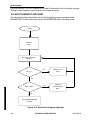
Instruction Buffer Usage Example . . . . . . . . . . . . . . . . . . . . . . . . . . . . . . . 16-5
16.5
Bootloader Flowchart . . . . . . . . . . . . . . . . . . . . . . . . . . . . . . . . . . . . . . . . . 16-6
x
MC68EZ328 USERÕS MANUAL
MOTOROLA
16.6
Special Notes . . . . . . . . . . . . . . . . . . . . . . . . . . . . . . . . . . . . . . . . . . . . . . . 16-7
SECTION 17
APPLICATION GUIDE
17.1
17.2
Design Checklist. . . . . . . . . . . . . . . . . . . . . . . . . . . . . . . . . . . . . . . . . . . . . 17-1
Using the MC68EZ328ADS Board . . . . . . . . . . . . . . . . . . . . . . . . . . . . . . . 17-2
SECTION 18
ELECTRICAL CHARACTERISTICS
18.1
MAXIMUM RATINGs . . . . . . . . . . . . . . . . . . . . . . . . . . . . . . . . . . . . . . . . . 18-1
18.2
DC ELECTRICAL CharacteristicS . . . . . . . . . . . . . . . . . . . . . . . . . . . . . . . 18-1
18.3
AC ELECTRICAL Characteristics. . . . . . . . . . . . . . . . . . . . . . . . . . . . . . . . 18-2
18.3.1
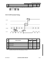
CLKO reference to Chip-Select Signals Timing . . . . . . . . . . . . . . . . . . 18-2
18.3.2
Chip-Select Read Cycle Timing . . . . . . . . . . . . . . . . . . . . . . . . . . . . . . 18-3
18.3.3
Chip-Select Write Cycle Timing . . . . . . . . . . . . . . . . . . . . . . . . . . . . . . 18-4
18.3.4
Chip-Select Flash Write Cycle Timing. . . . . . . . . . . . . . . . . . . . . . . . . . 18-5
18.3.5
DRAM Read Cycle 16-Bit Access (CPU Bus Master). . . . . . . . . . . . . . 18-6
18.3.6
DRAM Write Cycle 16-Bit Access (CPU Bus Master) . . . . . . . . . . . . . . 18-7
18.3.7
DRAM Hidden Refresh Cycle (Normal Mode). . . . . . . . . . . . . . . . . . . . 18-8
18.3.8
DRAM Hidden Refresh Cycle (Low Power Mode) . . . . . . . . . . . . . . . . 18-9
18.3.9
LCD SRAM/ROM DMA Cycle 16-Bit Mode Access(1 ws) ( . . . . . . . . 18-10
18.3.10 LCD DRAM DMA Cycle 16-Bit EDO Mode Access (LCD Bus Master)18-11
18.3.11 LCD DRAM DMA Cycle 16-Bit Page Mode Access (LCD Bus Master)18-12
18.3.12 LCD Controller Timing. . . . . . . . . . . . . . . . . . . . . . . . . . . . . . . . . . . . . 18-13
18.3.13 Normal Mode Timing. . . . . . . . . . . . . . . . . . . . . . . . . . . . . . . . . . . . . . 18-14
18.3.14 Normal Mode and Emulation Mode Timing. . . . . . . . . . . . . . . . . . . . . 18-14
18.3.15 Emulation Mode Timing . . . . . . . . . . . . . . . . . . . . . . . . . . . . . . . . . . . 18-14
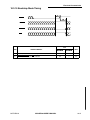
18.3.16 Bootstrap Mode Timing . . . . . . . . . . . . . . . . . . . . . . . . . . . . . . . . . . . . 18-15
SECTION 19
MECHANICAL DATA AND ORDERING INFORMATION
19.1
19.2
19.3
19.4
19.5
Ordering Information. . . . . . . . . . . . . . . . . . . . . . . . . . . . . . . . . . . . . . . . . . 19-1
TQFP Pin Assignments . . . . . . . . . . . . . . . . . . . . . . . . . . . . . . . . . . . . . . . 19-2
TQFP Package Dimensions . . . . . . . . . . . . . . . . . . . . . . . . . . . . . . . . . . . . 19-2
PBGA Pin Assignments . . . . . . . . . . . . . . . . . . . . . . . . . . . . . . . . . . . . . . . 19-4
PBGA Package Dimensions. . . . . . . . . . . . . . . . . . . . . . . . . . . . . . . . . . . . 19-4
MOTOROLA
MC68EZ328 USERÕS MANUAL
xi
xii
MC68EZ328 USERÕS MANUAL
MOTOROLA
LIST OF ILLUSTRATIONS
Figure
Number
1-1
1-2
1-3
1-4
2-1
2-2
4-1
4-2
5-1
5-2
5-3
6-1
7-1
7-2
8-1
8-2
9-1
10-1
10-2
11-1
11-2
11-3
11-4
12-1
12-2
12-3
12-4
13-1
14-1
14-2
MOTOROLA
Title
Page
Number
MC68EZ328 Block Diagram . . . . . . . . . . . . . . . . . . . . . . . . . . . . . . . . . . 1-2
User Programming Model . . . . . . . . . . . . . . . . . . . . . . . . . . . . . . . . . . . . 1-3
Supervisor Programming Model Supplement . . . . . . . . . . . . . . . . . . . . . 1-3
MC68EZ328 System Memory Map . . . . . . . . . . . . . . . . . . . . . . . . . . . . . 1-9
Signals Grouped by Function . . . . . . . . . . . . . . . . . . . . . . . . . . . . . . . . . 2-2
Typical Crystal Connection . . . . . . . . . . . . . . . . . . . . . . . . . . . . . . . . . . . 2-4
Chip-Selects and Memory Types . . . . . . . . . . . . . . . . . . . . . . . . . . . . . . 4-1
Size Selection and Memory Protection for CSB0 and CSB1 . . . . . . . . . 4-3
PLL Block Diagram . . . . . . . . . . . . . . . . . . . . . . . . . . . . . . . . . . . . . . . . . 5-1
Power Control Module Block Diagram . . . . . . . . . . . . . . . . . . . . . . . . . . 5-7
Power Control Operation. . . . . . . . . . . . . . . . . . . . . . . . . . . . . . . . . . . . . 5-8
Interrupt Processing Flowchart . . . . . . . . . . . . . . . . . . . . . . . . . . . . . . . . 6-2
Parallel Port Operation . . . . . . . . . . . . . . . . . . . . . . . . . . . . . . . . . . . . . . 7-1
Interrupt Port Operation . . . . . . . . . . . . . . . . . . . . . . . . . . . . . . . . . . . . . 7-7
Pulse-Width Modulator Block Diagram . . . . . . . . . . . . . . . . . . . . . . . . . . 8-1
Audio Waveform Generation. . . . . . . . . . . . . . . . . . . . . . . . . . . . . . . . . . 8-2
General-Purpose Timer Block Diagram . . . . . . . . . . . . . . . . . . . . . . . . . 9-1
Serial Peripheral Interface Master Block Diagram . . . . . . . . . . . . . . . . 10-1
Serial Peripheral Interface Master Operation . . . . . . . . . . . . . . . . . . . . 10-2
UART Block Diagram . . . . . . . . . . . . . . . . . . . . . . . . . . . . . . . . . . . . . . 11-2
NRZ ASCII ÒAÓ Character with Odd Parity . . . . . . . . . . . . . . . . . . . . . . 11-2
IrDA ASCII ÒAÓ Character with Odd Parity. . . . . . . . . . . . . . . . . . . . . . . 11-3
Baud Rate Generator Block Diagram . . . . . . . . . . . . . . . . . . . . . . . . . . 11-6
LCD Controller Block Diagram . . . . . . . . . . . . . . . . . . . . . . . . . . . . . . . 12-2
LCD Interface Timing for 4-, 2-, and 1-Bit Data Widths. . . . . . . . . . . . . 12-4
LCD Screen Format . . . . . . . . . . . . . . . . . . . . . . . . . . . . . . . . . . . . . . . 12-5
Mapping Memory Data on the Screen . . . . . . . . . . . . . . . . . . . . . . . . . 12-6
Real-Time Clock Block Diagram . . . . . . . . . . . . . . . . . . . . . . . . . . . . . . 13-2
DRAM Controller Block Diagram . . . . . . . . . . . . . . . . . . . . . . . . . . . . . 14-1
DRAM Address Multiplexer Options. . . . . . . . . . . . . . . . . . . . . . . . . . . 14-2
MC68EZ328 USERÕS MANUAL
xiii
14-3
14-4
15-1
15-2
15-3
15-4
16-1
16-2
19-1
xiv
LCD Controller and DRAM Controller Interface . . . . . . . . . . . . . . . . . . 14-4
Data Retention for the Reset Cycle . . . . . . . . . . . . . . . . . . . . . . . . . . . 14-5
In-Circuit Emulation Module Block Diagram . . . . . . . . . . . . . . . . . . . . . 15-1
Typical Emulator Design Example . . . . . . . . . . . . . . . . . . . . . . . . . . . . 15-9
Plug-in Emulator Design Example . . . . . . . . . . . . . . . . . . . . . . . . . . . 15-11
Application Development System Design Example . . . . . . . . . . . . . . 15-12
Bootstrap Mode Reset Timing . . . . . . . . . . . . . . . . . . . . . . . . . . . . . . . 16-2
Bootloader Program Operation . . . . . . . . . . . . . . . . . . . . . . . . . . . . . . . 16-6
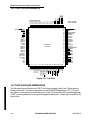
Top View . . . . . . . . . . . . . . . . . . . . . . . . . . . . . . . . . . . . . . . . . . . . . . . . 19-2
MC68EZ328 USERÕS MANUAL
MOTOROLA
LIST OF TABLES
Table
Number
1-1
1-2
1-3
2-1
6-1
6-2
11-1
11-2
11-3
12-1
13-1
MOTOROLA
Title
Page
Number
Address Modes . . . . . . . . . . . . . . . . . . . . . . . . . . . . . . . . . . . . . . . . . . . . 1-4
Instruction Set . . . . . . . . . . . . . . . . . . . . . . . . . . . . . . . . . . . . . . . . . . . . 1-5
ProgrammerÕs Memory Map . . . . . . . . . . . . . . . . . . . . . . . . . . . . . . . . . 1-10
Signal Function Groups. . . . . . . . . . . . . . . . . . . . . . . . . . . . . . . . . . . . . . 2-3
Exception Vector Assignment . . . . . . . . . . . . . . . . . . . . . . . . . . . . . . . . 6-3
Interrupt Vector Numbers . . . . . . . . . . . . . . . . . . . . . . . . . . . . . . . . . . . . 6-6
Non-Integer Prescaler Values . . . . . . . . . . . . . . . . . . . . . . . . . . . . . . . . 11-7
Non-Integer Prescaler Settings . . . . . . . . . . . . . . . . . . . . . . . . . . . . . . . 11-7
Selected Baud Rate Settings . . . . . . . . . . . . . . . . . . . . . . . . . . . . . . . . 11-7
Gray-Scale Palette Options. . . . . . . . . . . . . . . . . . . . . . . . . . . . . . . . . . 12-7
Sampling Timer Frequencies . . . . . . . . . . . . . . . . . . . . . . . . . . . . . . . . 13-3
MC68EZ328 USERÕS MANUAL
xv
xvi
MC68EZ328 USERÕS MANUAL
MOTOROLA
PREFACE
The MC68EZ328 (DragonBallEZ) microprocessor, which is the second generation of the
DragonBallª, is designed to save you time, power, cost, board space, pin count, and
programming steps when designing your product. This functionality on a different
microprocessor could require 20 separate components, each with 16-64 separate pins.
These components take up valuable space on your board and they also consume more
power. In addition, the signals between the CPU and a peripheral could be incompatible and
may not run from the same clock, which could require time delays or other special design
constraints.
All this combined makes the MC68EZ328 the microprocessor of choice among many
system designers. Its functionality and glue logic are all optimally connected, timed with the
same clock, fully tested, and uniformly documented. Also, only the essential signals are
brought out to the pins. The MC68EZ328Õs primary package consists of a surface-mount
plastic TQFP designed to leave the smallest possible footprint on your board.
RELATED DOCUMENTATION
This manual will discuss the details of how to initialize, configure, and program the
MC68EZ328 microprocessor. However, it assumes you have a basic knowledge of 68K
architecture. If you are not familiar with 68K, you should get a copy of the following
documents to use in conjunction with this manual.
¥ M68000 UserÕs Manual (part number M68000UM/AD).
¥ M68EZ328ADS UserÕs Manual, which is only available from our website.
¥ M68000 ProgrammerÕs Reference Manual (part number M68000PM/AD).
You can go to the Motorola website at www.mot.com/dragonball and download these
documents or you can contact your local sales office and request a printed version. The
website also has application notes that may be useful to you.
ORGANIZATION OF THIS MANUAL
This manual is organized according to the MC68EZ328 memory map, which is discussed in
Section 1.15 Memory Map.
MOTOROLA
MC68EZ328 USERÕS MANUAL
xvii
Preface
xviii
MC68EZ328 USERÕS MANUAL
MOTOROLA
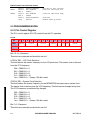
SECTION 1
BASIC ARCHITECTURE
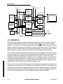
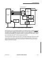
To improve total system throughput and reduce component count, board size, and cost of
system implementation, the MC68EZ328 combines a powerful MC68EC000 processor with
intelligent peripheral modules and a typical system interface logic. The architecture of the
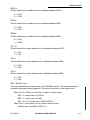
MC68EZ328 consists of the following blocks:
¥ EC000 core
¥ Chip-select logic and bus interface
¥ Phase-locked loop and power control
¥ Interrupt controller
¥ Parallel general-purpose I/O ports
¥ Pulse-width modulator
¥ General-purpose timer
¥ Serial peripheral interface
¥ UART and infra-red communication support
¥ LCD controller
¥ Real-time clock
¥ DRAM controller
¥ In-circuit emulation module
¥ Bootstrap mode
This manual assumes you are familiar with 68K architecture. If you are not, get a copy of the
M68000 UserÕs Manual (part number M68000UM/AD) and M68000 ProgrammerÕs
Reference Manual (part number M68000PM/AD) from your local Motorola sales office.
MOTOROLA
MC68EZ328 USERÕS MANUAL
1-1
Basic Architecture
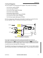
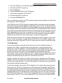
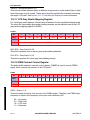
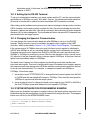
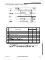
PARALLEL I/O PORTS
SYSTEM INTEGRATION MODULE
8-/16-BIT
68000 BUS
INTERFACE
ENHANCED
REAL-TIME
CLOCK
IN-CIRCUIT
EMULATION
INTERRUPT
CONTROLLER
DRAM
CONTROLLER
BOOTSTRAP
MODE
16-BIT
TIMER
MODULE
68EC000 HCMOS
STATIC
CORE
68EC000 INTERNAL BUS
PHASE-LOCKED
LOOP AND
POWER CONTROL
LCD
CONTROLLER
SPI
PWM
UART
WITH
INFRA-RED
SUPPORT
PARALLEL I/O PORTS
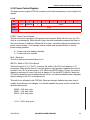
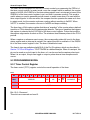
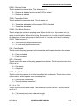
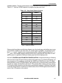
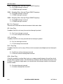
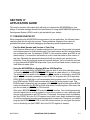
Figure 1-1. MC68EZ328 Block Diagram
1.1 CORE
The MC68EC000 core in the MC68EZ328 is an updated implementation of the M68000
32-bit microprocessor architecture. The main features of the core are:
¥ Low power, static HCMOS implementation
¥ 32-bit address bus and 16-bit data bus
¥ Sixteen 32-bit data and address registers
¥ 56 powerful instruction types that support high-level development languages
¥ 14 addressing modes and five main data types
¥ Seven priority levels for interrupt control
The core is completely code-compatible with other members of the M68000 families, which
means it has access to a broad base of established real-time kernels, operating systems,
languages, applications, and development tools.
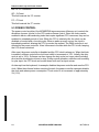
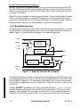
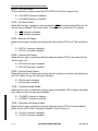
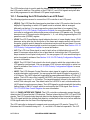
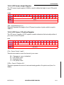
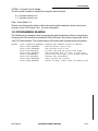
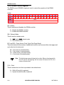
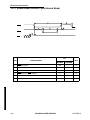
1.1.1 Core Programming Model
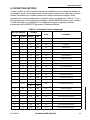
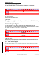
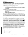
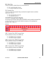
The core has 32-bit registers and a 32-bit program counter, which are shown in Figure 1-2.
The first eight registers (D7ÐD0) are data registers that are used for byte (8-bit), word
(16-bit), and long-word (32-bit) operations. When using the data registers to manipulate
data, they affect the status register (SR). The next seven registers (A6ÐA0) and the user
1-2
MC68EZ328 USERÕS MANUAL
MOTOROLA
Basic Architecture
stack pointer (USP) can function as software stack pointers and base address registers.
These registers can be used for word and long-word operations, but they do not affect the
status register. The D7-D0 and A6-A0 registers can be used as index registers.
31
16 15
8 7
0
D0
D1
D2
D3
D4
D5
D6
D7
31
31
16 15
DATA REGISTERS
0
16 15
A0
A1
A2
A3
A4
A5
A6
ADDRESS REGISTERS
A7 (USP)
USER STACK POINTER
PC
PROGRAM COUNTER
SR
STATUS REGISTER
0
31
0
7
0
Figure 1-2. User Programming Model
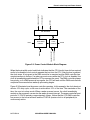
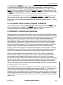
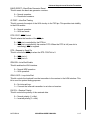
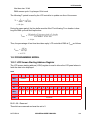
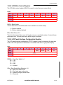
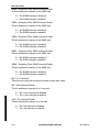
In supervisor mode, the upper byte of the status register and the supervisor stack pointer
(SSP) can also be programmed, as shown in Figure 1-3.
31
16 15
15
0
8 7
A7 (SSP)
SUPERVISOR STACK
POINTER
SR
STATUS REGISTER
0
Figure 1-3. Supervisor Programming Model Supplement
The status register contains the interrupt mask with seven available levels, as well as an
extend (X), negative (N), zero (Z), overflow (V), and carry (C) condition code. The T bit
indicates when the processor is in trace mode and the S bit indicates when it is in supervisor
or user mode.
MOTOROLA
MC68EZ328 USERÕS MANUAL
1-3
Basic Architecture
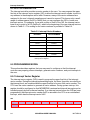
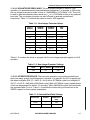
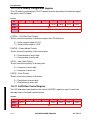
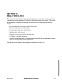
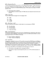
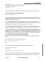
1.1.2 Data and Address Mode Types
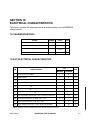
The core supports five types of data and six main types of address modes, as described in
the following tables.
DATA TYPES
ADDRESS MODE TYPES
Bits
Register direct
Binary-coded decimal digits
Register indirect
Bytes
Absolute
Words
Program counter relative
Long words
Immediate
Implied
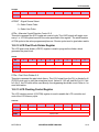
Table 1-1. Address Modes
ADDRESS MODE
SYNTAX
Register direct address
Data register direct
Address register direct
Dn
An
Absolute data address
Absolute short
Absolute long
xxx.W
xxx.L
Program counter relative address
Relative with offset
Relative with index offset
d16(PC)
d8(PC, Xn)
Register indirect address register
Register indirect
Postincrement register indirect
Predecrement register indirect
Register indirect with offset
Indexed register indirect with offset
(An)
(An)+
Ð(An)
d16(An)
d8(An, Xn)
Immediate data address
Immediate
Quick immediate
Implied address
Implied register
#xxx
#1Ð#8
SR/USP/SP/PC
NOTE:
Dn = Data Register
An = Address Register
Xn = Address or Data Register Used as Index Register
SR = Status Register
PC = Program Counter
SP = Stack Pointer
USP = User Stack Pointer
<> = Effective Address
d8 = 8-Bit Offset (Displacement)
d16 = 16-Bit Offset (Displacement)
#xxx = Immediate Data
1-4
MC68EZ328 USERÕS MANUAL
MOTOROLA
Basic Architecture
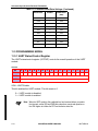
1.1.3 EC000 Instruction Set
The EC000 core instruction set supports high-level languages that facilitate programming.
Almost every instruction operates on bytes, words, and long-words, and most of them can
use any of the 14 address modes. By combining instruction types, data types, and address
modes, you can have access to over 1,000 instructions. These instructions include signed
and unsigned, multiply and divide, quick arithmetic operations, binary-coded decimal (BCD)
arithmetic, and expanded operations (through traps).
Table 1-2. Instruction Set
MNEMONIC
ABCD
DESCRIPTION
MNEMONIC
DESCRIPTION
Add decimal with extend
MOVEM
Move multiple registers
Add
MOVEP
Move peripheral data
ADDA
Add address
MOVEQ
Move quick
ADDQ
Add quick
ADDI
Add immediate
MOVE to SR
ADDX
Add with extend
MOVE to CCR
Move to condition codes
MOVE USP
Move user stack pointer
ADD
MOVE from SR Move from status register
Move to status register
AND
Logical AND
ANDI
AND immediate
MULS
Signed multiply
AND immediate to condition codes
MULU
Unsigned multiply
AND immediate to status register
NBCD
Negate decimal with extend
ANDI to CCR
ANDI to SR
ASL
Arithmetic shift left
ASR
Arithmetic shift right
NEGX
Bcc
Branch conditionally
NOP
No operation
BCHG
Bit test and change
NOT
Ones complement
BCLR
Bit test and clear
OR
Logical OR
BRA
Branch always
ORI
OR immediate
BSET
Bit test and set
ORI to CCR
BSR
Branch to subroutine
BTST
Bit test
CHK
Check register against bounds
CLR
Clear operand
ROL
Rotate left without extend
CMP
Compare
ROR
Rotate right without extend
CMPA
Compare address
ROXL
Rotate left with extend
CMPM
Compare memory
ROXR
Rotate right with extend
CMPI
Compare immediate
RTE
Return from exception
DBcc
Test cond, decrement and branch
RTR
Return and restore
DIVS
Signed divide
RTS
Return from subroutine
DIVU
Unsigned divide
MOTOROLA
NEG
ORI to SR
Negate
Negate with extend
OR immediate to condition codes
OR immediate to status register
PEA
Push effective address
RESET
Reset external devices
SBCD
MC68EZ328 USERÕS MANUAL
Subtract decimal with extend
1-5
Basic Architecture
Table 1-2. Instruction Set (Continued)
MNEMONIC
DESCRIPTION
EOR
Exclusive OR
EORI
Exclusive OR immediate
EORI to CCR
EORI to SR
MNEMONIC
Scc
Exclusive OR immediate to condition
codes
STOP
SUB
DESCRIPTION
Set conditional
Stop
Subtract
Exclusive OR immediate to status
register
SUBA
Subtract address
EXG
Exchange registers
SUBI
Subtract immediate
EXT
Sign extend
SUBQ
Subtract quick
JMP
Jump
SUBX
Subtract with extend
JSR
Jump to subroutine
SWAP
Swap data register halves
LEA
Load effective address
LINK
Link stack
LSL
Logical shift left
LSR
Logical shift right
MOVE
MOVEA
Move
TAS
TRAP
TRAPV
TST
UNLK
Test and set operand
Trap
Trap on overflow
Test
Unlink
Move address
1.2 CHIP-SELECT LOGIC AND BUS INTERFACE
The system control register (SCR) allows you to configure the system status and control
logic, register double-mapping, bus error generation, and module control register protection
on the MC68EZ328.
The MC68EZ328 contains eight programmable general-purpose chip-select signals. Each
chip-select block allows you to choose whether the chip-select allows read-only or both read
and write accesses, whether a DTACK signal is automatically generated for the chip-select,
the number of wait states (from zero to six) until the DTACK will be generated, and an 8- or
16-bit data bus.
The external bus interface handles the transfer of information between the internal core and
the memory, peripherals, or other processing elements in the external address space. It
consists of a 16-bit M68000 data bus interface for internal-only devices and an 8- or 16-bit
(or mixed) data bus interface to external devices.
1.3 PHASE-LOCKED LOOP AND POWER CONTROL
The clock synthesizer can operate with either an external crystal or an external oscillator
using an internal phase-locked loop (PLL). An external clock can also be used to directly
drive the clock signal at the operational frequency.
You can save power on the MC68EZ328 by turning off peripherals that are not being used,
reducing processor clock speed, or disabling the processor altogether. An interrupt at the
1-6
MC68EZ328 USERÕS MANUAL
MOTOROLA
Basic Architecture
interrupt controller logic that runs during low-power mode allows you to wake up from this
mode. Programmable interrupt sources cause the system to wake up. On-chip peripherals
can initiate a wake-up from doze mode and the external interrupts and real-time clock can
wake up the core from sleep mode.
1.4 INTERRUPT CONTROLLER
The interrupt controller prioritizes internal and external interrupt requests and generates a
vector number during the CPU interrupt-acknowledge cycle. Interrupt nesting is also
provided so that an interrupt service routine of a lower priority interrupt may be suspended
by a higher priority interrupt request. The on-chip interrupt controller has the following
features:
¥ Prioritized interrupts
¥ Fully nested interrupt environment
¥ Programmable vector generation
¥ Unique vector number generated for each interrupt level
¥ Interrupt/wakeup masking
1.5 PARALLEL GENERAL-PURPOSE I/O PORTS
The MC68EZ328 supports a maximum of 45 general-purpose I/O ports that you can
configure as general-purpose I/O pins or dedicated peripheral interface pins. Each pin can
be independently programmed as a general-purpose I/O pin even when other pins related
to that on-chip peripheral are used as dedicated pins. If all the pins for a particular peripheral
are configured as general-purpose I/O, the peripheral will still operate normally.
1.6 PULSE-WIDTH MODULATOR
The pulse-width modulator (PWM) can be used to generate sound. The 5-byte FIFO can
enhance performance by allowing the CPU to service other interrupts while data is being
supplied to the PWM.
1.7 GENERAL-PURPOSE TIMER
The free-running 16-bit timer can be used in various modes to capture the timer value with
an external event, to trigger an external event or interrupt when the timer reaches a set
value, or to count external events. The timer has an 8-bit prescaler to allow a programmable
clock input frequency to be derived from the system clock.
1.8 SERIAL PERIPHERAL INTERFACE
The serial peripheral interface (SPI) is mainly used for controlling external peripherals. The
passed data is synchronized with the SPI clock and it is transmitted and received with the
same SPI clock. The SPI module is only in master mode, which initiates SPI transfers from
the MC68EZ328 to the peripheral.
MOTOROLA
MC68EZ328 USERÕS MANUAL
1-7
Basic Architecture
1.9 UART AND INFRA-RED COMMUNICATION SUPPORT
The UART communicates with external devices with a standard asynchronous protocol at
baud rates from 300 bps to 1152 kpbs. The UART provides the pulses to directly drive
standard IrDA transceivers.
1.10 LCD CONTROLLER
The LCD controller is used to display data on an LCD module. It fetches display data from
memory and provides control signals, frame line pulse, clocks, and data to the LCD module.
It supports monochrome STN LCD modules with a maximum of sixteen gray levels with
frame rate control. System RAM can be used as display memory and DMA frees the CPU
from panel refresh responsibilities.
1.11 REAL-TIME CLOCK
A real-time clock provides time-of-day with one-second resolution. It uses the crystal (either
32.768 KHz or 38.4kHz) as a clock source to keep proper time. It keeps time as long as
power is applied to the chip, which can be in sleep or doze mode. The software watchdog
timer protects against system failures by providing a way for you to escape from unexpected
input conditions, external events, or programming errors. Once started, the software
watchdog timer must be cleared by software on a regular basis so that it never reaches its
time-out value. When it does reach its time-out value, the watchdog timer assumes that a
system failure has occurred and the software watchdog logic resets or interrupts the core.
1.12 DRAM CONTROLLER
The MC68EZ328 DRAM controller provides a glueless interface to most DRAM chips on the
market. It supports one or two banks of DRAM and each bank can be a maximum of 4
Mbyte.
1.13 IN-CIRCUIT EMULATION MODULE
The in-circuit emulation module is designed for low-cost emulator development purposes.
System memory space, which is 0xFFFC0000 to 0xFFFDFFFF, is covered by the EMUCS
signal and primarily dedicated to the emulator debug monitor. However, you can use the
EMUCS signal to select the monitor ROM or system I/O port. Keep in mind that if you select
the monitor ROM, the system must boot up in emulator mode.
1.14 BOOTSTRAP MODE
Bootstrapping allows you to use the UART port to download data/programs to system
memory without a preloaded monitor or boot code. You can also perform some simple
hardware debug functions on your target system using the bootstrap utility program
BBUG.EXE, which is available on our website.
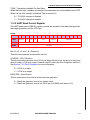
1.15 MEMORY MAP
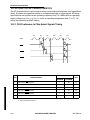
The memory map is a guide to all on-chip resources. Use the following figure and table as
a guide when you configure your chip. The base address used in the table is 0xFFFFFF00
and 0xFFF000 from reset. If a double-mapped bit is cleared in the system control register,
1-8
MC68EZ328 USERÕS MANUAL
MOTOROLA
Basic Architecture
then the base address is 0xFFFFF000. Unpredictable results occur if you write to any 4K
register space not documented in Table 1-3.
USERÕS MEMORY MAP
SUPERVISOR MEMORY MAP
MONITOR PROGRAM
(DEFINED BY USER)
512M
SYSTEM MEMORY
PROGRAM / DATA
MEMORY
0x1FFFFFFF
0xFFFC0000
0xFFFDFFFF
EMULATOR MONITOR
RESERVED
0xFFFFF000
MC68EZ328
REGISTER
0xFFFFF000
BOOTSTRAP
Figure 1-4. MC68EZ328 System Memory Map
MOTOROLA
MC68EZ328 USERÕS MANUAL
1-9
Basic Architecture
Table 1-3. ProgrammerÕs Memory Map
ADDRESS
NAME
WIDTH
DESCRIPTION
0xFFFFF000
SCR
8
System Control Register
0x1C
-2
0xFFFFF004
ID
32
Silicon ID Register
Ñ
Ñ
0xFFFFF100
CSGBA
16
Chip Select Group A Base Register
0x0000
-4
0xFFFFF102
CSGBB
16
Chip Select Group B Base Register
0x0000
-4
0xFFFFF104
CSGBC
16
Chip Select Group C Base Register
0x0000
-4
0xFFFFF106
CSGBD
16
Chip Select Group D Base Register
0x0000
-4
0xFFFFF110
CSA
16
Group A Chip-Select Register
0x00E0
-5
0xFFFFF112
CSB
16
Group B Chip-Select Register
0x0000
-5
0xFFFFF114
CSC
16
Group C Chip-Select Register
0x0000
-5
0xFFFFF116
CSD
16
Group D Chip-Select Register
0x0200
-5
0xFFFFF118
EMUCS
16
Emulation Chip-Select Register
0x0060
-8
0xFFFFF200
PLLCR
16
PLL Control Register
0x2430
-4
0xFFFFF202
PLLFSR
16
PLL Frequency Select Register
0x0123
-5
0xFFFFF204
RES
Ñ
Reserved
Ñ
Ñ
0xFFFFF207
PCTLR
8
Power Control Register
0x1F
-9
0xFFFFF300
IVR
8
Interrupt Vector Register
0x00
-6
0xFFFFF302
ICR
16
Interrupt Control Register
0x0000
-7
0xFFFFF304
IMR
32
Interrupt Mask Register
0x00FFFFFF
-9
0xFFFFF308
RES
32
Reserved
Ñ
Ñ
0xFFFFF30C
ISR
32
Interrupt Status Register
0x00000000
-11
0xFFFFF310
IPR
32
Interrupt Pending Register
0x00000000
-16
0xFFFFF400
PADIR
8
Port A Direction Register
0x00
-2
0xFFFFF401
PADATA
8
Port A Data Register
0x00
-2
0xFFFFF402
PAPUEN
8
Port A Pull-Up Enable Register
0xFF
-2
0xFFFFF403
RES
8
Reserved
Ñ
Ñ
0xFFFFF408
PBDIR
8
Port B Direction Register
0x00
-3
0xFFFFF409
PBDATA
8
Port B Data Register
0x00
-3
0xFFFFF40A
PBPUEN
8
Port B Pull-Up Enable Register
0xFF
-3
0xFFFFF40B
PBSEL
8
Port B Select Register
0xFF
-3
0xFFFFF410
PCDIR
8
Port C Direction Register
0x00
-5
0xFFFFF411
PCDATA
8
Port C Data Register
0x00
-5
0xFFFFF412
PCPDEN
8
Port C Pull-Down Enable Register
0xFF
-5
0xFFFFF413
PCSEL
8
Port C Select Register
0xFF
-5
0xFFFFF418
PDDIR
8
Port D Direction Register
0x00
-7
0xFFFFF419
PDDATA
8
Port D Data Register
0x00
-7
1-10
MC68EZ328 USERÕS MANUAL
RESET VALUE PAGE #
MOTOROLA
Basic Architecture
Table 1-3. ProgrammerÕs Memory Map (Continued)
ADDRESS
NAME
WIDTH
DESCRIPTION
0xFFFFF41A
PDPUEN
8
Port D Pull-Up Enable Register
0xFF
-7
0xFFFFF41B
PDSEL
8
Port D Select Register
0xF0
-7
0xFFFFF41C
PDPOL
8
Port D Polarity Register
0x00
-7
0xFFFFF41D
PDIRQEN
8
Port D Interrupt Request Enable Register
0x00
-7
0xFFFFF41E
PDKBEN
8
Port D Keyboard Enable Register
0x00
-7
0xFFFFF41F
PDIRQEG
8
Port D Interrupt Request Edge Register
0x00
-7
0xFFFFF420
PEDIR
8
Port E Direction Register
0x00
-10
0xFFFFF421
PEDATA
8
Port E Data Register
0x00
-10
0xFFFFF422
PEPUEN
8
Port E Pull-Up Enable Register
0xFF
-10
0xFFFFF423
PESEL
8
Port E Select Register
0xFF
-10
0xFFFFF428
PFDIR
8
Port F Direction Register
0x00
-12
0xFFFFF429
PFDATA
8
Port F Data Register
0x00
-12
0xFFFFF42A
PFPUEN
8
Port F Pull-Up Enable Register
0xFF
-12
0xFFFFF42B
PFSEL
8
Port F Select Register
0x00
-12
0xFFFFF430
PGDIR
8
Port G Direction Register
0x00
-14
0xFFFFF431
PGDATA
8
Port G Data Register
0x00
-14
0xFFFFF432
PGPUEN
8
Port G Pull-Up Enable Register
0x3D
-14
0xFFFFF433
PGSEL
8
Port G Select Register
0x08
-14
0xFFFFF500
PWMC
16
PWM Control Register
0x0020
-2
0xFFFFF502
PWMS
16
PWM Sample Register
0xxxxx
-5
0xFFFFF504
PWMP
8
PWM Period Register
0xFE
-5
0xFFFFF505
PWMCNT
8
PWM Counter Register
0x00
-6
0xFFFFF506
RES
16
Reserved
Ñ
Ñ
0xFFFFF600
TCTL
16
Timer Control Register
0x0000
-2
0xFFFFF602
TPRER
16
Timer Prescaler Register
0x0000
-4
0xFFFFF604
TCMP
16
Timer Compare Register
0xFFFF
-4
0xFFFFF606
TCR
16
Timer Capture Register
0x0000
-4
0xFFFFF608
TCN
16
Timer Counter Register
0x0000
-5
0xFFFFF60A
TSTAT
16
Timer Status Register
0x0000
-5
0xFFFFF800
SPIMDATA
16
SPIM Data Register
0x0000
-3
0xFFFFF802
SPIMCONT
16
SPIM Control/Status Register
0x0000
-4
0xFFFFF900
USTCNT
16
UART Status/Control Register
0x0000
-8
0xFFFFF902
UBAUD
16
UART Baud Control Register
0x003F
-11
0xFFFFF904
URX
16
UART Receiver Register
0x0000
-12
0xFFFFF906
UTX
16
UART Transmitter Register
0x0000
-14
MOTOROLA
MC68EZ328 USERÕS MANUAL
RESET VALUE PAGE #
1-11
Basic Architecture
Table 1-3. ProgrammerÕs Memory Map (Continued)
ADDRESS
NAME
WIDTH
DESCRIPTION
0xFFFFF908
UMISC
16
UART Miscellaneous Register
0x0000
-16
0xFFFFF90A
NIPR
16
UART Non-Integer Prescaler Register
0x0000
-18
0xFFFFFA00
LSSA
32
LCD Screen Starting Address Register
0x00000000
-9
0xFFFFFA05
LVPW
8
LCD Virtual Page Width Register
0xFF
-10
0xFFFFFA08
LXMAX
16
LCD Screen Width Register
0x03FF
-10
0xFFFFFA0A
LYMAX
16
LCD Screen Height Register
0x01FF
-11
0xFFFFFA18
LCXP
16
LCD Cursor X Position Register
0x0000
-11
0xFFFFFA1A
LCYP
16
LCD Cursor Y Position Register
0x0000
-12
0xFFFFFA1C
LCWCH
16
LCD Cursor Width and Height Register
0x0101
-12
0xFFFFFA1F
LBLKC
8
LCD Blink Control Register
0x7F
-13
0xFFFFFA20
LPICF
8
LCD Panel Interface Configuration Register
0x00
-13
0xFFFFFA21
LPOLCF
8
LCD Polarity Configuration Register
0x00
-14
0xFFFFFA23
LACDRC
8
LACD Rate Control Register
0x00
-14
0xFFFFFA25
LPXCD
8
LCD Pixel Clock Divider Register
0x00
-15
0xFFFFFA27
LCKCON
8
LCD Clocking Control Register
0x40
-15
0xFFFFFA29
LRRA
8
LCD Refresh Rate Adjustment Register
0xFF
-16
0xFFFFFA2B
RES
8
Reserved
Ñ
Ñ
0xFFFFFA2D
LPOSR
8
LCD Panning Offset Register
00
-17
0xFFFFFA31
LFRCM
8
LCD Frame Rate Control Modulation Register
0xB9
-17
0xFFFFFA33
LGPMR
8
LCD Gray Palette Mapping Register
0x84
-18
0xFFFFFA36
PWMR
16
PWM Contrast Control Register
0x0000
-18
0xFFFFFB00
RTCTIME
32
RTC Hours, Minutes, and Seconds Register
0x00000000
-4
0xFFFFFB04
RTCALRM
32
RTC Alarm Register
0x00000000
-5
0xFFFFFB0A
WATCHDOG
16
Watchdog Timer Register
0x0001
-5
0xFFFFFB0C
RTCCTL
8
RTC Control Register
0x00
-6
0xFFFFFB0E
RTCISR
8
RTC Interrupt Status Register
0x00
-7
0xFFFFFB10
RTCIENR
8
RTC Interrupt Enable Register
0x00
-9
0xFFFFFB12
STPWCH
8
Stopwatch Minutes Register
0x00
-11
0xFFFFFB1A
DAYR
16
RTC Day Count Register
0x0xxx
-12
0xFFFFFB1C
DAYALARM
16
RTC Day Alarm Register
0x0000
-12
0xFFFFFC00
DRAMMC
16
DRAM Memory Configuration Register
0x00000000
-6
0xFFFFFC02
DRAMC
16
DRAM Control Register
0x00000000
-8
0xFFFFFC80
RES
Ñ
Reserved
Ñ
Ñ
0xFFFFFD00
ICEMACR
32
ICEM Address Compare Register
0x00000000
-4
0xFFFFFD04
ICEMAMR
32
ICEM Address Mask Register
0x00000000
-4
1-12
MC68EZ328 USERÕS MANUAL
RESET VALUE PAGE #
MOTOROLA
Basic Architecture
Table 1-3. ProgrammerÕs Memory Map (Continued)
ADDRESS
NAME
WIDTH
DESCRIPTION
0xFFFFFD08
ICEMCCR
16
ICEM Control Compare Register
0x0000
-5
0xFFFFFD0A
ICEMCMR
16
ICEM Control Mask Register
0x0000
-5
0xFFFFFD0C
ICEMCR
16
ICEM Control Register
0x0000
-6
0xFFFFFD0E
ICEMSR
16
ICEM Status Register
0x0000
-8
0xFFFFFExx
Bootloader
Ñ
Bootloader Microcode Space
Ñ
-3
MOTOROLA
MC68EZ328 USERÕS MANUAL
RESET VALUE PAGE #
1-13
Basic Architecture
1-14
MC68EZ328 USERÕS MANUAL
MOTOROLA
SECTION 2
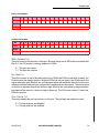
SIGNAL DESCRIPTIONS
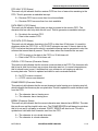
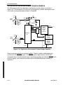
This section describes the MC68EZ328Õs input and output signals, which are organized into
functional groups, as illustrated in Figure 2-1. The MC68EZ328 uses a standard M68000
bus to communicate with on-chip and external peripherals, with an optional address
extension to the A23 signal. This single continuous bus exists both on and off the chip. Read
accesses made by the core to internal memory-mapped registers of the device are invisible
on the external bus, but write accesses made by the core to internal or external
memory-mapped locations are not invisible.
Note: The terms ÒassertionÓ and ÒnegationÓ are used extensively throughout this
section to avoid confusion when dealing with a mixture of active low and active
high signals. The terms ÒassertÓ and ÒassertionÓ are used to indicate that a signal
is active or true, regardless of whether that level is represented by a high or low
voltage. The terms ÒnegateÓ and ÒnegationÓ are used to indicate that a signal is
inactive or false.
MOTOROLA
MC68EZ328 USERÕS MANUAL
2-1
CLKO/PF2
PORT F
SYSTEM
INTEGRATION
MODULE
BUSW/DTACK/PG0
LWE
UWE
OE
TOUT/TIN/PB6
CSC0/RAS0/PB2
CSC1/RAS1/PB3
CSD0/CAS0/PB4
CSD1/CAS1/PB5
CSB0/PB0
CSB1/PB1
CSA0
CSA1/PF7
Signal Descriptions
PORT B
DRAM
CONTROLLER
CHIP-SELECT
A0/PG1
MD[12:0]/A[13:1]
68EC000 INTERNAL BUS
CLOCK
SYNTHESIZER
AND
POWER
CONTROL
PORT G
RESET
EMUIRQ/PG2
HIZ/P/D/PG3
EMUCS/PG4
EMUBRK/PG5
LCD
CONTROLLER
SERIAL
PERIPHERAL
INTERFACE
PWM
UART
WITH
INFRA-RED
SUPPORT
INTERRUPT
CONTROLLER
PROCESSOR
CONTROL,
EMULATION
AND
BOOT STRAP
PORTS C AND F
PORT E
PORT B
PWMO/PB7
INT0/PD0
INT1/PD1
INT2/PD2
INT3/PD3
IRQ1/PD4
IRQ2/PD5
IRQ3/PD6
IRQ6/PD7
IRQ5/PF1
PORTS D AND F
REAL-TIME
CLOCK
SPMTXD/PE0
SPMRXD/PE1
SPMCLK/PE2
DWE/UCLK/PE3
PLLGND
EXTAL
XTAL
PLLVDD
16-BIT
TIMER
LD0/PC0
LD1/PC1
LD2/PC2
LD3/PC3
LFLM/PC4
LLP/PC5
LCLK/PC6
LACD/PC7
LCONTRAST/PF0
A[23:20]/PF[6:3]
PORT F
D[7:0]/PA[7:0]
68EC000 HCMOS
STATIC
CORE
PORT A
D[15:8]
8-/16-BIT
68000 BUS
INTERFACE
PORT E
RXD/PE4
TXD/PE5
RTS/PE6
CTS/PE7
A[19:14]
Figure 2-1. Signals Grouped by Function
2-2
MC68EZ328 USERÕS MANUAL
MOTOROLA
Signal Descriptions
2.1 SIGNALS GROUPED BY FUNCTION
The MC68EZ328 signals are grouped according to their function in Table 2-1.
Table 2-1. Signal Function Groups
FUNCTION GROUP
SIGNALS
NUMBER OF PINS
Power
VDD, PLLVDD
6
Ground
VSS, PLLVSS
6
Clocks/PCIO
XTAL, EXTAL, CLKO/PF2
3
System Control
RESET
1
Address Bus/PFIO
PF[3:6]/A[23:20], A[19:14], A0/PG1, MD[12:0]/A[13:1]
24
Lower Data Bus/PAIO
PA[7:0]/D[7:0]
8
Upper Data Bus
D[15:6]
8
Bus Control/PCIO/PEIO
BUSW/DTACK/PG0, OE, LWE, UWE, DWE
5
Interrupt Controller/PMIO
INT0/PD0, INT1/PD1,INT2/PD2, INT3/PD3, IRQ1/PD4,
IRQ2/PD5, IRQ3/PD6, IRQ6/PD7, IRQ5/PF1
9
LCD Controller/PCIO
LACD/PC7, LCLK/PC6, LLP/PC5, LFLM/PC4,
LD[3:0]/PC[3:0], LCONTRAST/PF0
9
UART/PEIO
RXD/PE4, TXD/PE5, RTS/PE6, CTS/PE7, UCLK/PE3
5
Timer/PBIO
TOUT/TIN/PB6
1
Pulse-Width Modulator/PBIO
PWMO/PB7
1
Serial Peripheral Interface/PEIO
SPMTXD/PE0, SPMRXD/PE1, SPMCLK/PE2
3
Chip-Select
CSA[1:0]/PF7, CSB[1:0]/PB[0:1], CSC[1:0]/PB[3:2],
CSD[1:0]/PB[5:4]
8
Emulator Pins
EMUIRQ/PG2, EMUBRK/PG5, HIZ/P/D/PG3,
EMUCS/PG4
4
Note: All pins, except EXTAL, support TTL levels. When EXTAL is used as an input
clock, it needs a CMOS level. To ensure proper low-power operation, all inputs
should be driven to CMOS level. More power is consumed when you use a TTL
level to drive those inputs.
MOTOROLA
MC68EZ328 USERÕS MANUAL
2-3
Signal Descriptions
2.2 POWER AND GROUND SIGNALS
The MC68EZ328 microprocessor has 12 power supply pins. You should try to maintain a
low level of noise, potential crosstalk, and RF radiation from the output drivers.
¥ VDD has five power pins.
¥ VSS has five ground pins.
¥ PLLVDD has one power pin for the PLL.
¥ PLLVSS has one ground pin for the PLL.
2.3 CLOCK AND SYSTEM CONTROL SIGNALS
¥ EXTALÑExternal Clock/Crystal. This input signal connects to the external low
frequency crystal. The MC68EZ328 microprocessor supports both a 32.768kHz or
38.4kHz crystal frequency. For a 32.768kHz input, the internal phase-locked loop (PLL)
generates the PLL output clock at 16.58MHz. Figure 2-2 illustrates how a crystal is
usually connected to the MC68EZ328.
32.768kHz OR 38.4kHz
EXTAL
20pF
XTAL
20pF
Figure 2-2. Typical Crystal Connection
¥ XTALÑCrystal. This output signal connects the on-chip oscillator output to an external
crystal.
¥ CLKO/PF2ÑClock Out and Bit 2 of Port F. This output clock signal is derived from the
on-chip clock oscillator and is internally connected to the clock output of the internal
PLL. This signal is provided for external reference. The output can be disabled to
reduce power consumption and electromagnetic emission. This signal defaults to a PF2
input signal.
¥ RESETÑReset. This active-low schmitt trigger input signal resets the entire
MC68EZ328 processor (CPU and peripherals). After power-up, you should drive this
signal low for at least 250msec to ensure that the crystal oscillator starts and stabilizes.
This signal is inactive while the core is executing the reset instruction. When you are
using an R/C circuit to generate this input signal to the MC68EZ328, the R/C circuit
must be as close to the chip as possible.
2-4
MC68EZ328 USERÕS MANUAL
MOTOROLA
Signal Descriptions
2.4 ADDRESS BUS SIGNALS
The address bus pins A[23-0] are the address lines driven by the core or LCD controller for
panel refresh DMA. The internal chip-select module can decode a maximum 16M address
map. In sleep mode, all address signals are in an active state of the last bus cycle.
¥ A0/PG1ÑAddress 0 and Port G Bit 1. After system reset, this signal defaults to A0.
¥ A[19:14]ÑAddress Bits 19-14. These address output lines are not multiplexed with any
other I/O signal.
¥ A[23:20]/PF[6:3]ÑAddress Bits 23-20 and Port F Bits 6-3. These address lines are
multiplexed with I/O Port F. When programmed as I/O ports, they serve as generalpurpose I/O ports. Otherwise, they are output-only address signals. These signals
default to general-purpose I/O input and are pulled down with 100K resistors after reset.
2.5 DATA BUS SIGNALS
The flexible data bus interface design of the MC68EZ328 microprocessor allows you to
program the lower byte of the data bus (in an 8-bit-only system) as general-purpose I/O
signals. In sleep mode, all of the data bus pins (D15-D0) are individually pulled up with 100K
Ohms resistors.
¥ D[15:8]ÑData Bits 15-8. The upper byte of the data bus is not multiplexed with any
other signal. In pure 8-bit systems, this is the data bus. In mixed 8- and 16-bit systems,
8-bit memory blocks or peripherals should be connected to this bus.
¥ D[7:0]/PA[7:0]ÑData Bits 7-0 and Port A Bits 7-0. This bus is the lower data byte or
general-purpose I/O. In pure 8-bit systems, this bus can serve as a general-purpose
I/O. The WDTH8 bit in the system control register (0xFFF000) should be set to one by
software before the port can be used. In 16-bit or mixed 8- and 16-bit systems, these
pins must function as the lower data byte.
¥ MD[12:0]/A[13:1]ÑMultiplexed DRAM Bits 12-0 and Address Bits 13-1. These
address output lines are multiplexed with the DRAM row and column address signals.
The MD signal is selected on DRAM access cycles.
MOTOROLA
MC68EZ328 USERÕS MANUAL
2-5
Signal Descriptions
2.6 BUS CONTROL SIGNALS
¥ LWE, UWEÑLower Byte Write-Enable and Upper Byte Write-Enable. On a write cycle
to a 16-bit port, these active-low output signals indicate when the upper or lower eight
bits of the data bus contain valid data. In 8-bit mode or when the BSW bit in the
chip-select register is 0, use only the UWE signal for write-enable control. UWE can be
used as a DRAM write enable if DRAM refresh does not require that UWE stay high.
Otherwise, DWE should be used.
¥ DWE/UCLK/PE3ÑDRAM Write-Enable, UART Clock, and Port E Bit 3. Use the DWE
signal with DRAM, which requires an independent write-enable signal, rather than one
that is shared with UWE. This signal stays high during refresh cycles. This pin defaults
to a PE3 input signal. To select the DWE function, program Port E to DWE and enable
the DWE signal by writing a 1 to the DWE bit of the DRAMC register, which is described
in Section 14.2.2 DRAM Control Register. If this bit is not enabled, the UCLK signal
function is selected, which is an input clock to the UART module. For a description of
UCLK, refer to .
¥ BUSW/DTACK/PG0ÑBus Width, Data Transfer Acknowledge, Port G Bit 0. The
BUSW signal is the default bus width for the CSA0 signal. The DTACK signal is the
external input data acknowledge signal. The MC68EZ328 microprocessor will latch this
signal at the rising edge of the RESET signal. Its mode will determine the default bus
width for CSA0. For example, a logic low of BUSW on reset means that CSA0 connects
to an 8-bit memory device and a logic high of BUSW on reset means that CSA0
connects to a16-bit memory device. After reset, this pin defaults to the DTACK signal.
It can be configured as a DTACK function by programming the PGSEL register, which
is described in Section 7.2.7 Port G Registers. To generate a DTACK signal, refer to
Section 14.1.2 DTACK Generation. When external DTACK function is used to terminate
CPU cycles, an external 1K ohm pull-upresistor on this signal is required. The 1K ohm
pull-up resistor is not required when the system uses the internal DTACK for all chip
select signals.
¥ OEÑOutput Enable. This active-low signal is asserted during a read cycle of the
MC68EZ328 microprocessor, which enables the output of either ROM or SRAM.
2.7 INTERRUPT CONTROLLER SIGNALS
¥ INT[3:0], IRQ[3:1], IRQ6/PD[7:0]ÑInterrupt Bits 3-0, Interrupt Request Bits 3-1, and
Port D Bits 7-0. You can program these signals as interrupt inputs or parallel I/O ports.
When these signals are programmed to function as interrupts, they are schmitt trigger
inputs. To support keyboard applications, the I/O function can be used with interrupt
capabilities, which are described in Section 6.1 Interrupt Processing. The pin defaults
to a PDx input signal.
¥ IRQ5/PF1ÑInterrupt Request 5 and Port F Bit 1. This signal can be programmed to
either a parallel I/O or a schmitt trigger interrupt input. When it is configured as an
interrupt input it can be programmed as a level high or level low trigger interrupt.
2-6
MC68EZ328 USERÕS MANUAL
MOTOROLA
Signal Descriptions
2.8 LCD CONTROLLER SIGNALS
¥ LD[3:0]/PC[3:0]ÑLCD Data Bus Bits 3-0 and Port C Bits 3-0. This output bus transfers
pixel data to the LCD panel that it will be displayed on. The pixel data is arranged to
accommodate the programmable panel mode data width selection. Panel interfaces of
one, two, or four bits are supported. You can also program the output pixel data to be
inverted if it is required by your LCD panel.
The MC68EZ328Õs LCD interface data bus uses LD0 to display pixel 0, 0. Some LCD
panel manufacturers program their LCD panel data bus so that data bit 3 of the panel
displays pixel 0,0. For these panels, the connection between the MC68EZ328Õs LCD
data bus and the LCD panelÕs data bus could have a reversed bit significance. For these
panels, you must connect the MC68EZ328Õs LD0 signal to the LCD panelÕs data bit 3,
then connect LD1 to LCD data 2, LD2 to LCD data 1, and LD3 to LCD data 0. The four
pins can also be programmed as I/O ports from Port C. This pin defaults to a PCx input
signal pulled low.
¥ LFLM/PC4ÑFirst Line Marker and Port C Bit 4. This signal indicates the start of a new
display frame. LFLM becomes active after the first line pulse of the frame and remains
active until the next line pulse, at which point it deasserts and remains inactive until the
next frame. LFLM can be programmed to be an active-high or an active-low signal. It
can also be programmed as an I/O port.
¥ LLP/PC5ÑLCD Line Pulse and Port C Bit 5. This signal latches a line of shifted data
onto the LCD panel. It becomes active when a line of pixel data is clocked into the LCD
panel and remains asserted for eight pixel clock periods. LLP can be programmed to
be either an active-high or active-low signal. This pin can also be programmed as an
I/O port.
¥ LCLK/PC6ÑLCD Shift Clock and Port C Bit 6. This is the clock output to which the
output data to the LCD panel is synchronized. LCLK can be programmed to be either
an active-high or an active-low signal. This pin can also be programmed as an I/O port.
¥ LACD/PC7ÑLCD Alternate Crystal Direction and Port C Bit 7. This output is toggled to
alternate the crystal polarization on the panel. This signal can be programmed to toggle
at a period of 1 to 16 frames. This pin also can also be programmed as an I/O port.
¥ LCONTRAST/PF0ÑLCD Contrast and Port F Bit 0. This output controls the
pulse-width modulator (PWM) inside the LCD controller to adjust the supply voltage to
the LCD panel. This pin can also be programmed as an I/O port. This pin defaults to a
PFx input signal pulled high.
MOTOROLA
MC68EZ328 USERÕS MANUAL
2-7
Signal Descriptions
2.9 UART CONTROLLER SIGNALS
¥ RXD/PE4ÑUART Receive Data and Port E Bit 4. This pin is the receiver serial input.
During normal operation, NRZ data is expected, but in infra-red mode, a narrow pulse
is expected for each zero bit received. External circuitry must be used to convert the
infra-red signal to an electrical signal. RS-232 applications need an external RS-232
receiver to convert voltage levels. This pin defaults to a general-purpose PE4 input
signal.
¥ TXD/PE5ÑUART Transmit Data and Port E Bit 5. This pin is the transmitter serial
output. During normal operation, NRZ data is output, but in infra-red mode, a 3/16
bit-period pulse is output for each ÒzeroÓ bit transmitted. For RS-232 applications, this
pin must be connected to an RS-232 transmitter. For infra-red applications, this pin can
directly drive an infra-red LED. This pin defaults to a general-purpose PE5 input signal.
¥ RTS/PE6ÑRequest to Send and Port E Bit 6. This pin serves two purposes. Normally,
the receiver indicates that it is ready to receive data by asserting this pin (low). This pin
would be connected to the far-end transmitterÕs CTS pin. When the receiver detects a
pending overrun, it negates this pin. For other applications, this pin can be a
general-purpose output controlled by a bit in the URX register, which is described in
Section 11.3.3 UART Receiver Register. When it is programmed as parallel I/O, it
becomes PE6. This pin defaults to a general-purpose PE6 input signal.
¥ CTS/PE7ÑClear to Send and Port E Bit 7. This input controls the transmitter. Normally,
the transmitter waits until this signal is active (low) before a character is transmitted. If
the NOCTS bit is set in the UTX register, the transmitter sends a character whenever a
character is ready to transmit. See Section 11.3.4 UART Transmitter Register for more
information. This pin can then be used as a general-purpose input whose status is read
in the CTSSTAT bit of the UTX register. This pin can post an interrupt on any transition
of CTS, if enabled. This pin defaults to a CTS signal.
2.10 TIMER SIGNAL
¥ TOUT/TIN/PB6ÑTimer Output, Timer Input, and Port B Bit 6. This bidirectional signal
can be programmed to toggle or generate a pulse of one system clock duration when
timer/counter reaches a reference value. After reset, this pin defaults to a
general-purpose input PB6 signal.
2.11 PULSE-WIDTH MODULATOR SIGNAL
¥ PWMO/PB7ÑPulse Width Modulator Output and Port B Bit 7. This pin can serve as the
PWM output signal. When it is PWMO, it produces synthesized sound, which can be
connected to an audio amplifier and filter to generate melody and tone. This pin defaults
to a general-purpose PB7 input signal.
2.12 SERIAL PERIPHERAL INTERFACE SIGNALS
¥ SPMTXD/PE0ÑSPI Master Transmit Data and Port E Bit 0. This pin is the master SPI
shift register output signal. This pin defaults to a general-purpose PE0 input signal.
¥ SPMRXD/PE1ÑSPI Master Receive Data and Port E Bit 1. This pin is the input to the
master SPI shift register. This pin defaults to a general-purpose PE1 input signal.
2-8
MC68EZ328 USERÕS MANUAL
MOTOROLA
Signal Descriptions
¥ SPMCLK/PE2ÑSPI Master Clock and Port E Bit 2. This pin is the clock output when
the serial peripheral interface master is enabled. In polarity = 0 mode, this signal is low
while the serial peripheral interface master is idle. In polarity = 1 mode, this signal is
high during idle. This pin defaults to a general-purpose PE2 input signal.
2.13 CHIP-SELECT SIGNALS
¥ CSA0ÑChip-Select A Bit 0. CSA0 is a default chip-select signal after reset. It is set to
six wait-states and decodes all address ranges, except internal register address space
and emulator space (0xFFFC0000-0xFFFDFFFF). It can be reprogrammed during the
boot sequence to another address range or different wait-states. The default data bus
width for CSA0 is determined by the state of the BUSW signal.
¥ CSA1/PF7, CSB[1:0]/PB[1:0], CSC[1:0]/PB[3:2], CSD[1:0]/PB[5:4]ÑChip-Select A,
B, C, and D Bits 0 and 1, Port F Bit 7, Port B Bits 5-0. These pins comprise the
remainder of the Group A, B, C, and D chip-selects and are individually programmable.
Pins that are not needed as chip-selects can be programmed as general-purpose I/Os.
In addition, CSC[1:0] and CSD[1:0] are designed to support DRAM as CAS and RAS
signals. These pins default to a general-purpose input signal.
2.14 IN-CIRCUIT EMULATION SIGNALS
¥ HIZ/P/D/PG3ÑHigh Impedance, Program/Data, and Port G Bit 3. During system reset,
a logic low of this input signal will put the MC68EZ328 into Hi-Z mode, in which all
MC68EZ328 pins are three-stated after reset release. For normal operation, this pin
must be pulled high during system reset or left unconnected. This pin defaults to the
P/D function, but can be programmed as a general-purpose I/O. P/D is a status signal
that shows whether the current bus cycle is in program space or in data space during
emulation mode.
¥ EMUIRQ/PG2ÑEmulator Interrupt Request and Port G Bit 2. During system reset, a
logic low of this input signal will put the MC68EZ328 into emulation mode, which is
described in . For normal operation, this pin must be pulled high during system reset
or left unconnected. After system reset this pin defaults to an EMUIRQ function in
normal or emulation mode. EMUIRQ is an active low, level 7 interrupt input signal.
¥ EMUBRK/PG5ÑEmulator Breakpoint and Port G Bit 5. During system reset, a logic low
of this input signal will put the MC68EZ328 into bootstrap mode, which is described in
. For normal operation, this pin must be pulled high during system reset or left
unconnected. After system reset, this pin defaults to the EMUBRK function, which is an
I/O signal used in emulation mode for breakpoint control.
¥ EMUCS/PG4ÑEmulator Chip-Select and Port G Bit 4. EMUCS is an 8-bit data bus
width chip-select signal that selects the dedicated memory space from 0xFFFC0000 to
0xFFFDFFFF. It cannot be used to select 16-bit data bus memory devices. EMUCS is
not only activated in emulation mode, but in normal and bootstrap modes as well. See
for more information about EMUCS operation. This pin defaults to an EMUCS signal.
MOTOROLA
MC68EZ328 USERÕS MANUAL
2-9
Signal Descriptions
2-10
MC68EZ328 USERÕS MANUAL
MOTOROLA
SECTION 3
SYSTEM CONTROL
The MC68EZ328 microprocessor contains a system control register that enables the system
software to customize the following functions:
¥ Access permission from the internal peripheral registers
¥ Address space of the internal peripheral registers
¥ Bus time-out control and status (bus-error generator)
3.1 OPERATION
The on-chip resources use a reserved 4,096-byte block of address space for their registers.
This block is double-mapped to two locations at resetÑ0xFFFFF000 (32-bit) and 0xFFF000
(24-bit). The DMAP bit in the system control register disables double-mapping in a 32-bit
system. If you clear this bit, the on-chip peripheral registers appear only at the top of the 4G
address range starting at 0xFFFFF000.
The system control register allows you to control system operation functions like bus
interface and hardware watchdog protection. It contains status bits that allow exception
handler code to investigate the cause of exceptions and resets. The hardware watchdog
(bus time-out monitor) and the software watchdog timer provide system protection. The
hardware watchdog provides a bus monitor that causes a bus error when a bus cycle is not
terminated by the DTACK signal before 128 clock cycles have elapsed.
The bus error time-out logic consists of a watchdog counter that, when enabled, begins to
count clock cycles as the internal AS pin is asserted for internal or external bus accesses.
The negation of AS normally terminates the count, but if the count reaches terminal count
before AS is negated, BERR is asserted until AS is negated. The bus error time-out logic
uses one control bit and one status bit in the system control register. The BETO bit in the
system control register is set after a bus time-out, which could be caused by a write-protect
violation.
The software watchdog timer resets the MC68EZ328 if enabled and not cleared or disabled
before reaching terminal count. The software watchdog timer is enabled at reset.
MOTOROLA
MC68EZ328 USERÕS MANUAL
3-1
System Control
3.2 PROGRAMMING MODEL
3.2.1 System Control Register
The 8-bit read/write system control register (SCR) resides at 0xFFFFF000 after reset. The
SCR cannot be accessed in user data space if the SO bit is set to 1. Writing a 1 to the status
bits in this register clears them, but writing a 0 has no effect.
SCR
BIT
7
6
5
4
3
2
1
0
FIELD
BETO
WPV
PRV
BETEN
SO
DMAP
RESERVED
WDTH8
RESET
0x1C
ADDR
0x(FF)FFF000
BETOÑBus Error Time-Out
This status bit indicates whether or not a bus error timer time-out has occurred. When a bus
cycle is not terminated by the DTACK signal after 128 clock cycles have elapsed, the BETO
bit is set. However, the BETEN bit must be set for a bus error time-out to occur. This bit is
cleared by writing a 1 (writing a 0 has no effect).
0 = A bus error timer time-out did not occur.
1 = A bus error timer time-out occurs because an undecoded address space has been
accessed or because a write-protect or privilege violation has occurred.
WPVÑWrite-Protect Violation
This status bit indicates that a write-protect violation has occurred. If a write-protect violation
occurs and the BETEN bit is not set, the cycle will not terminate. The BETEN bit must be set
for a bus error exception to occur during a write-protect violation. This bit is cleared by
writing a 1 (writing a 0 has no effect).
0 = A write-protect violation did not occur.
1 = A write-protect violation has occurred.
PRVÑPrivilege Violation
This status bit indicates that If a privilege violation occurs and the BETEN bit is not set, the
cycle will not terminate. The BETEN bit must be set for a bus error exception to occur during
a privilege violation. This bit is cleared by writing a 1 (writing a 0 has no effect).
0 = A privilege violation did not occur.
1 = A privilege violation has occurred.
BETENÑBus-Error Time-Out Enable
This control bit enables the bus error timer.
0 = Disable the bus error timer.
1 = Enable the bus error timer.
3-2
MC68EZ328 USERÕS MANUAL
MOTOROLA
System Control
SOÑSupervisor Only
This control bit limits on-chip registers to supervisor accesses only.
0 = User and supervisor mode.
1 = Supervisor-only mode.
DMAPÑDouble Map
This control bit controls the double-mapping function.
0 = The on-chip registers are mapped at 0xFFFFF000Ð0xFFFFFFFF.
1 = The on-chip registers are mapped at 0xFFFFF000Ð0xFFFFFFFF and
0xFFF000Ð0xFFFFF.
Bit 1ÑReserved
This bit is reserved and reads 0.
WDTH8Ñ8-Bit Width Select
This control bit allows the D[7:0] pins to be used for port B input/output.
0 = Not an 8-bit system.
1 = 8-bit system.
MOTOROLA
MC68EZ328 USERÕS MANUAL
3-3
System Control
3-4
MC68EZ328 USERÕS MANUAL
MOTOROLA
SECTION 4
CHIP-SELECT LOGIC
The MC68EZ328 microprocessor contains eight general-purpose, programmable,
chip-select signals, which are arranged in four groups of twoÑ(CSA[1:0], CSB[1:0],
CSC[1:0], CSD[1:0]). Among them is a special-purpose chip-select signalÑCSA0Ñwhich
is also a boot device chip-select. From reset, all the addresses are mapped to CSA0 until
group base address A is programmed and the EN bit is set in the appropriate chip-select
register. From that point on, CSA0 does not decode globally and it is only asserted when
decoded from the programming information in the chip-select register. Group C
(CSC0/CSC1) and Group D (CSD0/CSD1) chip-selects are also special because they can
be programmed as row address strobe (RAS0/RAS1) and column address strobe
(CAS0/CAS1) for DRAM interface. For details, refer to and the chip-select group C and D
registers. For each memory area, you can define an internally generated cycle-termination
signal, called DTACK, with a programmable number of wait states. This feature saves board
space that would otherwise be used for cycle-termination logic.
With the mentioned chip-selects, the system can adopt flexible memory configuration based
on cost and availability. Up to four different classes of devices/memory can be used in a
system without external decode or wait-state generation logic. Specifically, 8- or 16-bit
combinations of ROM, SRAM, Flash memory, and DRAM are supported, as shown in
Figure 4-1.
CSA0
ROM, SRAM, FLASH MEMORY CHIP-SELECT
CSA1
ROM, SRAM, FLASH MEMORY CHIP-SELECT
CSB0
ROM, SRAM, FLASH MEMORY CHIP-SELECT
CSB1
ROM, SRAM, FLASH MEMORY CHIP-SELECT
CSC0/RAS0
DRAM, ROM, SRAM, FLASH MEMORY CHIP-SELECT
CSC1/RAS1
DRAM, ROM, SRAM, FLASH MEMORY CHIP-SELECT
CSD0/CAS0
DRAM, ROM, SRAM, FLASH MEMORY CHIP-SELECT
CSD1/CAS1
DRAM, ROM, SRAM, FLASH MEMORY CHIP-SELECT
Figure 4-1. Chip-Selects and Memory Types
The basic chip-select model allows the chip-select output signal to assert in response to an
address match. The signals are asserted externally shortly after the internal AS signal goes
low. The address match is described in terms of a group base address register and a
MOTOROLA
MC68EZ328 USERÕS MANUAL
4-1
Chip-Select Logic
chip-select register. The memory size of the chip-select can be selected from a set of
predefined ranges (32K, 64K, 128K, 256K, 512K, 1M, 2M, and 4M). These memory ranges
represent the most popular memory sizes available on the market and apply to CSBx,
CSCx, and CSDx. For CSA0, since it mainly supports ROM, which is usually 128K to 16M.
With this scheme, you can easily design software without dealing with the chip-select mask
register. You can choose whether the chip-select allows read-only or read/write accesses,
whether a DTACK signal is automatically generated for the chip-select, the number of wait
states (from zero to six), and data bus size selection.
4.1 CHIP-SELECT OPERATION
A chip-select output signal is asserted when an address is matched and after the AS signal
goes low. The base address and address mask registers are used in the compare logic to
generate an address match. The byte size of the matching block must be a power of two and
the base address must be an integer multiple of this size. Therefore, an 8K block size must
begin on an 8K boundary and a 64K block size can only begin on a 64K boundary. Each
chip-select is programmable and the registers have read/write capability so that the
programmed values can be read back.
Note:
The chip-select logic does not allow an address match during interrupt
acknowledge (Function Code 7) cycles.
4.1.1 Memory Protection
The chip-select range of the four chip-selects can be programmed as read-only or read/
write. For chip-selects that control the crucial system data, they are usually programmed as
supervisor-only and read-only so it can be protected from system misuse (e.g. low battery).
However, a certain area of this chip-select controlled area can be programmed as read/
write, which provides optimal memory use, as shown in Figure 4-2. This area can be defined
by programming the UPSIZ bits in the CSB, CSC, and CSD registers to between 32K and
256K.
4-2
MC68EZ328 USERÕS MANUAL
MOTOROLA
Chip-Select Logic
UNPROTECTED MEMORY (READ/WRITE)
UP TO 256KB
MEMORY
MAP
RAM
CSB0
UP TO 16M
CSB1
UP TO 16M
PROTECTED MEMORY
(SUPERVISOR-ONLY, READ-ONLY)
Figure 4-2. Size Selection and Memory Protection for CSB0 and CSB1
4.1.2 Programmable Data Bus Size
Each chip-select can be configured to address an 8- or 16-bit space. You can mix 16- and
8-bit contiguous address memory devices on a 16-bit data bus system. If the core performs
a 16-bit data transfer in an 8-bit memory space, then two 8-bit cycles will occur. However,
the address and data strobes remain asserted until the end of the second 8-bit cycle. In this
case, only the external core data bus upper byte (D[15:8]) is used and the least-significant
bit of the address (A0) increments automatically from one to the next. A0 should be ignored
in 16-bit data-bus cycles even if only the upper or lower byte is being read or written. For an
external peripheral that only needs an 8-bit data bus interface and does not require
contiguous address locations (unused bytes on empty addresses), use a chip-select
configured to a 16-bit data bus width and connect to the D[7:0] pins. This balances the load
of the two data bus halves in an 8-bit system. The internal data bus is16 bits wide. All internal
registers can be read or written in a zero wait-state cycle.
Each chip-select defaults to a 16-bit data bus width. The BSW field of the chip-select option
register enables 16- and 8-bit data bus widths for each of the 16 chip-select ranges. You can
select the initial bus width for the boot chip-select by placing a logic 0 or 1 on the BUSW pin
at reset to specify the width of the data bus. This allows a boot EPROM of the data bus width
to be used in any given system. All external accesses that do not match one of the
chip-select address ranges are assumed to be a 16-bit device. That is just one access
performed for a 16-bit transfer. It can also be a 8-bit port accessed every other byte.
The boot chip-select is initialized from reset to assert in response to any address except the
on-chip register space (0xFFFFF000 to 0xFFFFFFFF). This ensures that a chip-select to the
boot ROM or EPROM will fetch the reset vector and execute the initialization code, which
should set up the chip-select ranges.
A logic 0 on the BUSW pin sets the boot deviceÕs data bus to 8 bits wide and a logic 1 sets
it to 16 bits wide. At reset, the data bus port size for CSA0 and the data width of the boot
ROM device are determined by the state of BUSW. The other chip-selects are initialized to
MOTOROLA
MC68EZ328 USERÕS MANUAL
4-3
Chip-Select Logic
be nonvalid, so they will not assert until they are programmed and the EN bit is set in the
chip-select registers.
Note: If the group address and chip-select registers are programmed to overlap, the
chip-select signals will overlap too. Unused chip-selects must be programmed to
0 wait-states and 16 bits wide. Map them to dummy space if necessary. When
you are configuring the chip-select signals, the core can be set to write to a
read-only location. This prevents the chip-select and DTACK signals from not
being asserted, but the internal BERR signal to be asserted, if a bus error timer
is enabled.
4.1.3 Overlapping Chip-Select Registers
You should not program the group address and chip-select registers to overlap. If you do,
the chip-select signals will overlap. Unused chip-selects must be disabled. Map them to an
unused space, if possible.
When the CPU tries to write to a read-only location that you have programmed, the
chip-select and DTACK signals will not be generated internally. BERR will be asserted
internally if the bus error time-out function is enabled.
Note:
The chip-select logic does not allow an address match during interrupt
acknowledge cycles.
4.2 PROGRAMMING MODEL
The chip-select module contains registers that you can use to control external devices, such
as memory. Chip-selects do not operate until the register in a particular group of devices is
initialized and the EN bit is set in the corresponding chip-select register. The only exception
is the CSA0 signal, which is the boot device chip-select.
4.2.1 Chip-Select Group Base Address Registers
There are four 16-bit chip-select group base address A-D (CSGBA-CSGBD) registers in the
chip-select module (one for each chip-select group). These registers define the address at
which the chip-select starts. For example, the CSA0 signal can start at 0x000000 if you
program the CSGBA register and CSA1 returns the selected memory size apart from CSA0.
CSGBA-CSGBD
BIT
FIELD
15
14
GBA28 GBA27
13
12
11
10
9
8
7
6
5
4
3
2
1
0
GBA26
GBA25
GBA24
GBA23
GBA22
GBA21
GBA20
GBA19
GBA18
GBA17
GBA16
GBA15
GBA14
Ñ
RESET
0x0000
ADDR
0x(FF)FFF100, 102, 104, 106
4-4
MC68EZ328 USERÕS MANUAL
MOTOROLA
Chip-Select Logic
GBAxÑGroup Base Address 28Ð14
This field (the upper 15 bits of each base address register) selects the starting address for
the chip-select address range. The GBAx field is compared to the address on the address
bus to determine if the group is decoded. The chip-select base address must be set
according to the size of the corresponding chip-select signals of the group. For example, if
CSA1 and CSA0 are each assigned a 2M memory space, the CSGBA register must be set
in a 4M space boundary, such as system address 0x0, 0x4M, 0x8M and so on. It cannot be
set at 0x1M, 0x2M, 0x3M, 0x5M, etc.
Bit 0ÑReserved
This bit is reserved and should be set to 0.
4.2.2 Chip-Select Registers
There are four 16-bit chip-select (CSA, CSB, CSC, and CSD) registers for each
corresponding chip-select base address register. Each of these registers controls two
chip-select signals and can be configured to select the memory type, size of the memory
range supported, and to program the required wait-states or use the external DTACK signal.
CSA
BIT
15
FIELD
RO
14
13
12
11
10
9
Ñ
8
7
6
5
4
3
2
1
0
FLASH
BSW
WS2
WS1
WS0
SIZ2
SIZ1
SIZ0
EN
RESET
0x0000
ADDR
0x(FF)FFF110
CSB AND CSC
BIT
15
14
13
12
11
FIELD
RO
SOP
ROP
UPSIZ
1
UPSIZ
0
10
9
Ñ
8
7
6
5
4
3
2
1
0
FLASH
BSW
WS2
WS1
WS0
SIZ2
SIZ1
SIZ0
EN
RESET
0x0000
ADDR
0x(FF)FFF112 AND 0x114
CSD
BIT
15
14
13
12
11
10
9
8
7
6
5
4
3
2
1
0
FIELD
RO
SOP
ROP
UPSIZ
1
UPSIZ
0
COMB
DRAM
FLASH
BSW
WS2
WS1
WS0
SIZ2
SIZ1
SIZ0
EN
RESET
0x0200
ADDR
0x(FF)FFF1116
MOTOROLA
MC68EZ328 USERÕS MANUAL
4-5
Chip-Select Logic
ROÑRead Only
This bit sets the chip-select to read-only. Otherwise, read and write accesses are allowed.
A write to a read-only area will generate a bus error if the BETEN bit of the SCR is set. See
Section 3.2.1 System Control Register for more information.
0 = Read/write.
1 = Read-only.
SOPÑSupervisor-Only for Protected Memory Block
This bit sets the protected memory block to supervisor-only. Otherwise, supervisor and user
accesses are allowed. If you access the supervisor-only area, you will get a bus error if the
BETEN bit of the SCR is set. See Section 3.2.1 System Control Register for more
information.
0 = Supervisor/user.
1 = Supervisor-only.
ROPÑRead-Only for Protected Memory Block
This bit sets the protected memory block to read-only. Otherwise, read and write accesses
are allowed. If you write to a read-only area, you will get a bus error.
0 = Read/write.
1 = Read-only.
UPSIZÑUnprotected Memory Block Size
This field determines the unprotected memory range of the chip-select.
00 =
01 =
10 =
11 =
32K.
64K.
128K.
256K.
COMBÑCombining
This bit controls combining RAS0 and RAS1 memory space to generate RAS0. When this
bit is set to 1, RAS1 can be used as a general-purpose I/O signal.
0 = RAS0 to RAS0 memory space.
1 = RAS0 covers both RAS0 and RAS1 memory space B.
4-6
MC68EZ328 USERÕS MANUAL
MOTOROLA
Chip-Select Logic
DRAMÑDRAM Selection
This bit is used to select the RAS and CAS signals.
0 = Select CSC[1:0] and CSD[1:0].
1 = Select CAS and RAS.
Note: To configure the CSC register as a non-DRAM memory type, you must clear the
DRAM bit of the CSD register.
FLASHÑFlash Memory Support
To support Flash memory, this bit forces the LWE/UWE signal to go active after chip-select.
0 = The chip-select and LWE/UWE signals go active at the same clock edge.
1 = The chip-select signal goes low one clock before LWE/UWE.
BSWÑData Bus Width
This bit sets the data bus width for this chip-select area.
0 = 8-bit.
1 = 16-bit.
WSÑWait-State
This field determines the number of wait-states added before an internal DTACK signal is
returned for this chip-select.
000 =
001 =
010 =
011 =
100 =
101 =
110 =
111 =
Zero wait states.
One wait state.
Two wait states.
Three wait states.
Four wait states.
Five wait states.
Six wait states.
External DTACK.
Note: When using the external DTACK signal, you must configure the
BUSW/DTACK/PG0 pin.
MOTOROLA
MC68EZ328 USERÕS MANUAL
4-7
Chip-Select Logic
SIZÑChip-Select Size
This field determines the memory range of the chip-select. For CSAx and CSBx, the
chip-select size is between 128K and 16M. For CSCx and CSDx, the chip-select size is
between 32K and 4M.
000 =
001 =
010 =
011 =
100 =
101 =
110 =
111 =
128K (32K for CSCx and CSDx).
256K (64K for CSCx and CSDx).
512K (128K for CSCx and CSDx).
1M (256K for CSCx and CSDx).
2M (512K for CSCx and CSDx).
4M (1M for CSCx and CSDx).
8M (2M for CSCx and CSDx).
16M (4M for CSCx and CSDx).
ENÑChip-Select Enable
This write-only bit enables each chip-select.
0 = Disabled.
1 = Enabled.
4.2.3 Emulation Chip-Select Register
In addition to the eight general-purpose chip-select signals, the MC68EZ328 has an
emulation chip-select register (EMUCS) that is specifically designed for the in-circuit
emulation module. This register only provides wait-states 6-0, depending on the type of chip
you are using. You can also use the external logic (DTACK) to have longer wait-states.
EMUCS is only valid for the 0xFFFC0000-0xFFFDFFFF memory location.
EMUCS
BIT
FIELD
15
14
13
12
11
10
9
8
7
Ñ
RESET
0x0060
ADDR
0x(FF)FFF118
4-8
6
5
4
WS2
WS1
WS0
MC68EZ328 USERÕS MANUAL
3
2
1
0
Ñ
MOTOROLA
Chip-Select Logic
WSÑWait-State 2Ð0
This field determines the number of wait states added before an internal DTACK is returned
for this chip-select.
000 = Zero wait states.
001 = One wait state.
010 = Two wait states.
011 = Three wait states.
100 = Four wait states.
101 = Five wait states.
110 = Six wait states.
111 = External DTACK.
Note: When using the external DTACK signal, you must configure the
BUSW/DTACK/PG0 pin.
4.3 PROGRAMMING EXAMPLE
This following fragment of software code demonstrates how to initialize the chip-select with
a particular memory configuration.
************************************************
*
Chip-Select registers
************************************************
REGSBASE
equ
0xFFFFF000
internal registers base address
BASEA
equ
REGSBASE+0x100
group A base register
BASEB
equ
REGSBASE+0x102
group B base register
BASEC
equ
REGSBASE+0x104
group C base register
BASED
equ
REGSBASE+0x106
group D base register
CSA
equ
REGSBASE+0x110
group A chip select register
CSB
equ
REGSBASE+0x112
group B chip select register
CSC
equ
REGSBASE+0x114
group C chip select register
CSD
equ
REGSBASE+0x116
group D chip select register
************************************************
*
PORT control registers
************************************************
PORTBASE
equ
REGSBASE+0x400
port B registers base address
PBDir
equ
PORTBASE+0x08
port B direction register
PBData
equ
PORTBASE+0x09
port B data register
PBPU
equ
PORTBASE+0x0A
port B pullup enable register
PBSel
equ
PORTBASE+0x0B
port B select register
************************************************
*
Initialization
************************************************
START
move.b
#0x00,PBSel
disable PortB, select chip selects
move.w
move.w
#0x0000,BASEA
#0x8081,CSA
set base address 0x0000000
read-only,16-bit,0 wait-state,128K
move.w
#0x2000,BASEB
set base address 0x4000000
MOTOROLA
MC68EZ328 USERÕS MANUAL
4-9
Chip-Select Logic
move.w
#0x0093,CSB
read/write,16-bit,1 wait-state,256K
move.w
move.w
#0x2040,BASEC
#0x0191,CSC
set base addrs 0x4080000
read/write,flash,16-bit,1 ws,32K
move.w
#0x0000,CSD
config CSC,CSD as non-DRAM memory type
* The above initialization will configurate the CSA and CSB chip selects as
* follows :
*
*
CSA0 0x0000000-0x001ffff,read-only, 16-bit,0 wait-state,128K
*
CSA1 0x0020000-0x003ffff,read-only, 16-bit,0 wait-state,128K
*
CSB0 0x4000000-0x403ffff,read/write,16-bit,1 wait-state,256K
*
CSB1 0x4040000-0x407ffff,read/write,16-bit,1 wait-state,256K
*
CSC0 0x4080000-0x4087fff,read/write,flash,16-bit,1 wait-state, 32K
*
CSC1 0x4088000-0x408ffff,read/write,flash,16-bit,1 wait-state, 32K
*
CSD0 disabled
*
CSD1 disabled
4-10
MC68EZ328 USERÕS MANUAL
MOTOROLA
SECTION 5
PHASE-LOCKED LOOP AND POWER CONTROL
The phase-locked-loop (PLL) generates all of the clocks for the MC68EZ328
microprocessor. It includes a crystal oscillator that can be used with low-frequency crystals.
The PLL generates a high-frequency master clock that is phase-locked to the crystal
reference. The features of the PLL are:
¥ Fully static HCMOS technology
¥ Programmable clock synthesizer using a 32.768kHz or 38.4kHz crystal for full
frequency control
¥ Low-power stop capabilities
¥ Modules can be individually shut down
¥ Lowest power mode control
The PLL is a flexible clock source for the MC68EZ328. It provides a crystal-controlled
master clock at 32kHz frequencies that are no lower than 13MHz. The master clock can be
divided down to provide a system clock as low as a sixteenth of the voltage-controlled
oscillator (VCO) frequency. The low-frequency reference clock (32.768kHz or 38.4kHz) is
always available to the real-time clock or timer. The PLL can be disabled to save power, but
it can be reenabled within 1ms of a wakeup interrupt. The PLL, used in conjunction with the
power control block, provides an efficient power-control mechanism for the MC68EZ328
microprocessor, as illustrated in Figure 5-1.
MPU BUS
PHASE LOCKED
WAKEUP
MPU INTERFACE
DMACLK
EXTAL
XTAL
CRYSTAL
OSCILLATOR
PHASE-LOCKED VCO
LOOP
PRESCALER
DIVIDER
DIVIDER
SYSCLK
DIVIDER
LCDCLK
CLK32
Figure 5-1. PLL Block Diagram
MOTOROLA
MC68EZ328 USERÕS MANUAL
5-1
Phase-Locked Loop and Power Control
5.1 OPERATION
5.1.1 Using the PLL To Reduce Power Consumption
The PLL uses a dual-modulus prescaler to reduce power consumption. This approach
divides the VCO frequency by 14 before it is fed to the rest of the divider chain.
Dual-modulus counters operate differently from other counters in that the overall divide ratio
depends on two separate valuesÑP and Q. Besides the power-saving advantage, above a
divisor of 397 (decimal), every divisor is available to fine-tune the VCO in 32kHz steps. The
formula for the dual-modulus divider is:
Divisor = 14 (P + 1) + Q + 1
where
1 <= Q <= 14
P >= Q + 1
The minimum divisor is P=0x1B, Q=0x04 (397 decimal). This produces 13.008896MHz.
5.1.2 PLL Operation at Power-Up
At initial power-up, the crystal oscillator begins oscillating within several hundred
milliseconds. While reset remains asserted, the PLL begins the lockup sequence and locks
1ms before the crystal oscillator becomes stable. Once lockup occurs, the VCO frequency
is 16.580608 MHz, assuming that a 32.768 kHz crystal is used. When using a 38.400 kHz
crystal the VCO frequency is 19.430400MHz. The system clock is reset to VCO divided by
2 as a result of the default setting of the PRESC bitin the LL control register. The boot
sequence must change the VCO frequency to less than 16.7MHz and clear the PRESC bit
before activating any modules or changing the chip-select wait-state settings.
To generate the master frequency, multiply the reference (32.768kHz) by the PLL divisor.
The default divisor is 506. The divisor can be changed under software control, which is
described in Section 5.1.4 Changing the VCO Frequency.
Note: The default divider value (506) was selected because it can directly generate
standard baud frequencies at a better than 0.1% accuracy rate.
5.1.3 PLL Operation at Wake-Up
When the MC68EZ328 is awakened from sleep mode by a wake-up event, the PLL achieves
lock within 1ms. The crystal oscillator is always on after initial power-up, so the crystal
startup time is not a factor. The master clock starts operating once the PLL achieves lock.
5-2
MC68EZ328 USERÕS MANUAL
MOTOROLA
Phase-Locked Loop and Power Control
5.1.4 Changing the VCO Frequency
To change the VCO frequency, you should use the sequence below. It assumes all
peripherals have been disabled and that the CPU is operating at the highest possible
frequency (SYSCLK SEL = 100). NEWFREQ is the new frequency value (P and Q values)
to be programmed. This routine enables the timer to wake the PLL up after two CLK32
ÒticksÓ. When the PLL wakes up, it will be at the new frequency. The interrupt service routine
for the temporary timer interrupt should clear the timer interrupt and then return. In addition,
the master frequency should only be changed during an early phase of the boot-up
sequence. Keep in mind, this code was written for clarity, not efficiency.
NEWFREQ
PLLCONTROL
PLLFREQ
TCOMPARE
TCONTROL
IMR
equ
equ
equ
equ
equ
equ
somevalue
$FFF200
$FFFF202
$FFF604
$FFF600
$FFF304
;P and Q value of new frequency
;PLL Control Register
;PLL Frequency Control Register
;Timer Compare Value Register
;Timer Control Register
;Interrupt Mask Register
move.l IMR,-(SP)
;save the Interrupt Mask register
move.l #$fffffffd,IMR
;enable ONLY Timer interrupt
move.w #$0001,TCOMPARE ;set compare value to 2
move.w #$0119,TCONTROL ;enable Timer 2 with CLK32 source
SYNC1
btst.b #$7,PLLFREQ
;synchronize to CLK32 high level
beq.s SYNC1
;CLK32 is still not high, go back
SYNC2
btst.b #$7,PLLFREQ
;synchronize to CLK32 low level
bne.s SYNC2
;CLK32 is still not low, go back
move.w #NEWFREQ,PLLFREQ ;load the new frequency
ori.b #$8,PLLCONTROL+1 ;disable the PLL (in 30 clocks)
stop #$2000
;stop, enable all interrupts
; the PLL shuts down here and waits for the Timer interrupt
; interrupt service for Timer occurs here
move.w (SP)+,IMR
;restore the Interrupt Mask Register
rts
;PLL is now at the new frequency
; The PLL has reacquired lock and SYSCLK is stable
5.1.5 PLL Operation at System Shut-Down
Shutting the PLL down to place the system in sleep mode is similar to the process used to
change the frequency. The difference is that the system can be awakened only by a
wake-up event or reset. Before shutting the PLL down, make sure that all peripheral devices
are prepared for shut-down. The PLL shuts down 30 clocks after the DISPLL bit is set in the
PL control register so that there is enough time to execute the stop instruction. When a
wake-up event occurs, the PLL is enabled and within 1ms it acquires lock and the system
clock begins. The CPU executes an interrupt service routine for the level of the wake-up
event.
After the rte instruction in the wake-up service routine, the CPU returns and starts execution
on the instruction following the stop instruction. The instruction sequence below illustrates
a typical shut-down sequence. It assumes that all peripherals have been shut down before
the PLL is stopped.
MOTOROLA
MC68EZ328 USERÕS MANUAL
5-3
Phase-Locked Loop and Power Control
SYNC1
SYNC2
move.w
btst.b
bne.s
btst.b
beq.s
move.w
stop
#$2410,$FFF200
#$7,$FFF202
SYNC1Ó,
#$7,SFFF202
SYNC2
#$2418,$FFF200
#$2000
;Set PLL to full running
;look for 32K clock low
;look for 32K clcok high
;Stop PLL
;enable wake up event
5.2 PROGRAMMING MODEL
5.2.1 PLL Control Register
The PLL control register (PLLCR) controls how the PLL operates.
PLLCR
BIT
FIELD
15
14
RESERVED
13
12
LCDCLK SEL
11
10
9
8
7
SYSCLK SEL
6
RESERVED
RESET
0x2420
ADDR
0x(FF)FFF200
5
PRES
C
4
3
CLKEN DISPLL
2
1
0
RESERVED
Bits 15Ð14ÑReserved
These bits are reserved and should be set to 0.
LCDCLK SELÑLCD Clock Selection
This field selects the master frequency for the LCD pixel clock. The master clock is derived
from the VCO frequency.
000 =
001 =
010 =
011 =
1xx =
DMACLK Ö 2.
DMACLK Ö 4.
DMACLK Ö 8.
DMACLK Ö 16.
DMACLK Ö 1 (binary 100 after reset).
SYSCLK SELÑSystem Clock Selection
This field selects the master frequency for the MC68EZ328 microprocessor system clock.
The master clock is derived from the VCO frequency. This field can be changed at any time.
The VCO frequency is unaffected by changes.
000 =
001 =
010 =
011 =
1xx =
DMACLK Ö 2.
DMACLK Ö 4.
DMACLK Ö 8.
DMACLK Ö 16.
DMACLK Ö 1 (binary 100 after reset).
Bits 7Ð6ÑReserved
These bits are reserved and should be set to 0.
5-4
MC68EZ328 USERÕS MANUAL
MOTOROLA
Phase-Locked Loop and Power Control
PRESCÑPrescaler
This field selects the frequency for the LCD controllerÕs DMA clock and the other two dividers
inside the MC68EZ328. This clock is derived from the VCO frequency. This field can be
changed at any time.
0 = VCO Ö 1.
1 = VCO Ö 2.
CLKENÑClock Enable
This bit enables the CLKO pin.
0 = CLKO/PF2 disabled.
1 = CLKO/PF2 enabled (default).
DISPLLÑDisable PLL
This bit, when set, disables the PLL. The system clock is shut down and the MC68EZ328
assumes its lowest power state. Only the 32kHz clock runs. Refer to Section 5.1.5 PLL
Operation at System Shut-Down for a description of the preferred method for system clock
shut-down. Once the PLL is disabled, only a wake-up interrupt or reset can reenable it.
0 = PLL enabled (default).
1 = PLL disabled.
Bits 2Ð0ÑReserved
These bits must remain at their default value.
5.2.2 PLL Frequency Select Register
The PLL frequency select register (PLLFSR) controls the two dividers of the dual-modulus
counter. While this register can be accessed as bytes, it should always be written as a 16-bit
word.
PLLFSR
BIT
15
14
FIELD
CLK3
2
PROT
13
12
RESERVED
11
10
9
8
7
6
QC
5
4
3
2
1
0
PC
RESET
0x0123
ADDR
0x(FF)FFF202
CLK32ÑClock 32
This read-only bit indicates the current status of the CLK32 signal and can be used to
synchronize the software to the 32kHz reference clock.
PROTÑProtect
This bit protects the ÒPÓ and ÒQÓ counter values from additional writes. After this bit is set by
software, the frequency select register cannot be written. Only a reset clears this bit.
MOTOROLA
MC68EZ328 USERÕS MANUAL
5-5
Phase-Locked Loop and Power Control
Bits 13Ð12ÑReserved
QCÑQ Count
This field controls the ÒQÓ counter.
PCÑP Count
This field controls the ÒPÓ counter.
5.3 POWER CONTROL
The power control module of the MC68EZ328 improves power efficiency as it controls the
allocation of power (clocks) to the CPU under software control. Since the clocks can be
enabled in bursts, while executing tasks that require significant CPU resources, they can be
enabled for extended periods of time. While the CPU is relatively idle, the clock can be
disabled or bursted with a low duty-cycle. When a wake-up event occurs, the clock is
immediately enabled, allowing the CPU to service the request. The DMA controller is not
affected by the power controller. It has full access to the bus while the CPU is idle, keeping
the LCD screen refreshed.
After reset, the power controller is disabled and the CPU clock is always on. When the block
is enabled, software controls the clock burst width in increments of 1/31. Initially, the dutycycle is set to 100%. Software can then change the duty-cycle to a lower value (including
zero) and the clock begins to burst or stop. During normal operation, while the core is waiting
for your input, the CPU clock can be shut down until such an input arrives.
An interrupt from the keyboard, for example, disables the power controller and runs the CPU
clock. When the software finishes servicing the task, the power controller can again disable
the clock and reduce power consumption. Clock control is in increments of approximately
3% (1/31).
5-6
MC68EZ328 USERÕS MANUAL
MOTOROLA
MPU BUS
CPU BUS GRANT
CPU BUS REQUEST
Phase-Locked Loop and Power Control
MPU INTERFACE
CLK68K
DMA BUS GRANT
CLOCK
CONTROL
DMA BUS REQUEST
BURST WIDTH
CONTROL
WAKEUP
CLK32
Figure 5-2. Power Control Module Block Diagram
When the burst-width control sub-block indicates that the CPU clockÕs time-slot has expired
and is to be disabled, clock control requests the bus from the CPU. After the bus is granted,
the clock stops. A bus grant to the DMA controller is asserted and the DMA controller has
complete access to the bus. If a wake-up event occurs while the CPU clock is disabled, the
clock is immediately enabled and the CPU processes the event. The DMA controller always
has priority, so if a DMA access is in progress, the CPU will wait until the DMA controller has
completed its access before wake-up processing begins.
Figure 5-3 illustrates how the power controller operates. In this example, the clock bursts at
about a 15% duty-cycle, so the core is active about 15% of the time. The remainder of the
time, the core is in sleep mode. When a wake-up event occurs, the clock immediately
restarts so the processor can service the wake-up event interrupt. The power controller burst
period is 31 CLK32 periods or approximately 1msec. Notice that the LCD DMA controller
has access to the bus at all times and the SYSCLK (master clock to all peripherals) is
continuously active.
MOTOROLA
MC68EZ328 USERÕS MANUAL
5-7
Phase-Locked Loop and Power Control
1MSEC
SYSCLK
CPU ACTIVE
WAKEUP EVENT
CPU SLEEP
CPU ACTIVE
CPU SLEEP
CPU ACTIVE
CPU SLEEP
CPU ACTIVE
CPUCLK
Figure 5-3. Power Control Operation
5.3.1 Operating the Power Control Module
The power control module has three modes of operation:
¥ Normal
¥ Doze
¥ Sleep
5.3.1.1 NORMAL MODE. When the MC68EZ328 microprocessor starts operating after
reset, the power control module is disabled and the CPU clock runs continuously. To reduce
the power consumed by the core, set the PCEN bit in the PCTLR register. The value of the
WIDTH bit in the PCTLR register determines the duty-cycle of the clock burst that is applied
to the core. If a wake-up event is received, the power control module is immediately disabled
and continuous clocks are supplied. It is up to the wake-up service routine to reenable the
power control module.
5.3.1.2 DOZE MODE. The coreÕs clock can be disabled for extended periods of time by
setting the WIDTH bit to 00000. The coreÕs clock is immediately enabled when it receives a
wake-up event. At the end of the service routine, the power control module can be
reenabled, putting the core back into doze mode. Once the CPU clock is disabled, only a
wake-up event or hardware reset will reenable it. For various core resource requirements,
you can program the duty-cycle register for burst-duty cycles of any value between 0/31 and
31/31. This effectively provides a variable clock frequency (and power dissipation) between
0% and 100% of the system clock frequency in 3% incremental steps.
The most effective power control strategy is to run the CPU at the highest system speed until
no CPU cycles are needed, then enter doze mode. You can do this by writing 0x80 into the
power control register. This disables the CPU clock at the earliest possible moment, but
allows the CPU to immediately respond to wake-up events. The peripheral devices,
including the LCD controller, are not affected by the power control module.
5.3.1.3 SLEEP MODE. The PLL is disabled in sleep mode. Only the 32kHz clock works to
keep the real-time clock operational. Wake-up events activate the PLL and the system clock
starts operating after 1msec.
5-8
MC68EZ328 USERÕS MANUAL
MOTOROLA
Phase-Locked Loop and Power Control
5.3.2 Power Control Register
The power control register (PCTLR) is used to control how much power you are using in the
system.
PCTLR
BIT
7
6
5
FIELD
PCEN
RESERVED
0
4
3
2
1
0
WIDTH
RESET
0x001F
ADDR
0x(FF)FFF207
PCENÑPower Control Enable
This bit controls the operation of the power control module. While this bit is low, the CPU
clock is on continuously. While this bit is high, the width comparator presents the clock to
the core in bursts or disables it. When this bit is clear, a masked interrupt can disable the
power control module. Your interrupt service routine must reenable this bit to reenter
power-saving operation.
0 = Power control is disabled (default).
1 = Power control is enabled.
Bit 6ÑReserved
This bit is reserved and should be set to 0.
WIDTHÑWidth of CPU Clock Bursts
This field resets to 11111 (0x1F). It controls the width of the CPU clock bursts in 1/31
increments. While this bit is set to 1 and the power control module is enabled, the clock is
bursted to the CPU at a duty-cycle of 1/31. When the WIDTH field is 1F(hex), the clock is
always on and when it is zero, the clock is always off. Set the WIDTH field to 0 when the
CPU will be disabled for an extended amount of time. You can immediately wake it up again
without waiting for the PLL to reacquire lock.
This field is not affected by the PCEN bit. When an interrupt disables the power control
module, these bits are not changed. You should reenable the power control module that
services the interrupt.
00000 = 0/31 duty-cycle.
00001 = 1/31 duty-cycle.
00010 = 2/31 duty-cycle.
¥
¥
¥
11111 = 31/31 duty-cycle.
MOTOROLA
MC68EZ328 USERÕS MANUAL
5-9
Phase-Locked Loop and Power Control
5-10
MC68EZ328 USERÕS MANUAL
MOTOROLA
SECTION 6
INTERRUPT CONTROLLER
The interrupt controller supports 18 edge- and level-sensitive interrupts. There are seven
interrupt levels. Level 7 has the highest priority and level 1 has the lowest. Interrupts can
originate from the following sources:
¥ EMUIRQ (level 7)
¥ IRQ6 external interrupt (level 6)
¥ Timer (level 6)
¥ Pulse-width modulator (level 6)
¥ IRQ5 external interruptÐpen (level 5)
¥ Serial peripheral interface (level 4)
¥ UART needs serviceÐtransmit or receive (level 4)
¥ Software watchdog timer interrupt (level 4)
¥ Real-time clock interrupt (level 4)
¥ Real-time clock sampling interrupt (level 4)
¥ Keyboard interrupt (level 4)
¥ General-purpose interrupt INT[3:0] (level 4). These pins can be used as keyboard
interrupts.
¥ IRQ3 external interrupt (level 3)
¥ IRQ2 external interrupt (level 2)
¥ IRQ1 external interrupt (level 1)
6.1 INTERRUPT PROCESSING
Interrupts are processed in the following sequence on the MC68EZ328:
1. The interrupt controller collects interrupt events from on- and off-chip peripherals,
prioritizes them, and presents the highest priority request to the core processor if there
are no higher interrupts pending. Otherwise, the higher interrupt will be served first.
2. The core processor responds to the interrupt request by executing an interrupt
acknowledge bus cycle after the completion of the current instruction.
3. The interrupt controller recognizes the interrupt acknowledge (IACK) cycle and places
the interrupt vector for that interrupt request onto the core processor bus.
MOTOROLA
MC68EZ328 USERÕS MANUAL
6-1
Interrupt Controller
4. The core processor reads the vector and address of the interrupt handler in the
exception vector table and begins execution at that address.
EXTERNAL OR INTERNAL
INTERRUPT
INTERRUPT
CONTROLLER
2
PRIORITIZES
INTERRUPT
HIGHER
INTERRUPT
3
1
NO
EC000 CORE
4
0xFFF.....
YES
INTERRUPT
HANDLER
PROCESS
INTERRUPT
Figure 6-1. Interrupt Processing Flowchart
Steps 2 and 4 are the responsibility of the core processor, whereas steps 1 and 3 are the
responsibility of the interrupt controller. External devices are forbidden from responding to
IACK cycles with a vector because it is the responsibility of the interrupt controller.
On the MC68EZ328, steps 2 and 4 operate exactly as they would on other M68000 devices,
which are described in the M68000 UserÕs Manual. In step 2, the core processorÕs status
register (SR) is available to mask interrupts globally or to determine which priority levels can
currently generate interrupts. Also in step 2, the interrupt acknowledge cycle is executed.
In step 4, the core processor reads the vector number, multiplies it by four to get the vector
address, fetches a 4-byte program address from that vector address, and then jumps to that
4-byte address. This 4-byte address is the location of the first instruction in the interrupt
handler.
The interrupt priority is based on the interrupt level. The interrupts with the same interrupt
level are prioritized by the software during the execution of the interrupt service routine. The
MC68EZ328 provides one interrupt vector for each interrupt level. You can program the
most-significant five bits of the interrupt vector, but the lower three bits reflect the interrupt
level that is being serviced. All interrupts are maskable. Writing a 1 to a bit in the interrupt
mask register disables that interrupt. If an interrupt is masked, you can find out its status in
the interrupt pending register.
6-2
MC68EZ328 USERÕS MANUAL
MOTOROLA
Interrupt Controller
6.2 EXCEPTION VECTORS
A vector number is an 8-bit number that can be multiplied by four to obtain the address of
an exception vector. An exception vector is the memory location from which the processor
fetches the address of a software routine that is used to handle an exception. Each
exception has a vector number and an exception vector, as described in Table 6-1. User
interrupts are part of the exception processing on the MC68EZ328 and the vector numbers
for user interrupts are configurable. For additional information regarding exception
processing, see the M68000 ProgrammerÕs Reference Manual.
Table 6-1. Exception Vector Assignment
VECTORS NUMBERS
ADDRESS
SPACE
ASSIGNMENT
000
SP
Reset: Initial SSP
4
004
SP
Reset: Initial PC
2
8
008
SD
Bus Error
3
3
12
00C
SD
Address Error
4
4
16
010
SD
Illegal Instruction
5
5
20
014
SD
Divide-by-Zero
6
6
24
018
SD
CHK Instruction
7
7
28
01C
SD
TRAPV Instruction
8
8
32
020
SD
Privilege Violation
9
9
36
024
SD
Trace
A
10
40
028
SD
Line 1010 Emulator
B
11
44
02C
SD
Line 1111 Emulator
C
12
48
030
SD
Unassigned, Reserved
D
13
52
034
SD
Unassigned, Reserved
E
14
56
038
SD
Unassigned, Reserved
F
15
60
03C
SD
Uninitialized Interrupt Vector
64
040
10Ð17
16Ð23
SD
Unassigned, Reserved
92
05C
HEX
DECIMAL
DECIMAL
HEX
0
0
0
1
1
2
18
24
96
060
SD
Spurious Interrupt
19
25
100
064
SD
Level 1 Interrupt Autovector
1A
26
104
068
SD
Level 2 Interrupt Autovector
1B
27
108
06C
SD
Level 3 Interrupt Autovector
1C
28
112
070
SD
Level 4 Interrupt Autovector
1D
29
116
074
SD
Level 5 Interrupt Autovector
1E
30
120
078
SD
Level 6 Interrupt Autovector
1F
31
124
07C
SD
Level 7 Interrupt Autovector
MOTOROLA
MC68EZ328 USERÕS MANUAL
6-3
Interrupt Controller
Table 6-1. Exception Vector Assignment (Continued)
20Ð2F
30Ð3F
40ÐFF
128
080
188
0BC
192
0C0
255
0FF
256
100
1020
3FC
32Ð47
48Ð63
64Ð255
SD
TRAP Instruction Vectors
SD
Unassigned, Reserved
SD
User Interrupt Vectors
NOTES:
1.Vector numbers 12Ð14, 16Ð23, and 48Ð63 are reserved for future enhancements by Motorola.
None of your peripheral devices should be assigned to these numbers.
2.Reset vector 0 requires four words, unlike the other vectors which only require two words, and it is located in
the supervisor program space.
3.The spurious interrupt vector is taken when there is a bus error indication during interrupt processing.
4.TRAP #n uses vector number 32+ n (decimal).
5.SP denotes supervisor program space and SD denotes supervisor data space.
Note: The MC68EZ328 does not provide autovector interrupts. At system start-up, you
need to program the user interrupt vector so that the processor can handle
interrupts properly.
6.3 RESET
The reset exception corresponds to the highest exception level. A reset exception is
processed for system initialization and to recover from a catastrophic failure. Any processing
that is in progress at the time of the reset is aborted and cannot be recovered. Neither the
program counter nor the status register is saved. The processor is forced into the supervisor
state. The interrupt priority mask is set at level 7. The address in the first 2 words of the reset
exception vector is fetched by the processor as the initial SSP (Supervisor Stack Pointer),
and the address in the next two words of the reset exception vector is fetched as the initial
program counter.
At start-up or reset, the default chip-select (CSA0) is asserted and all other chip-selects are
negated. You should use CSA0 to decode an EPROM/ROM memory space. In this case,
the first two long-words of the EPROM/ROM memory space should be programmed to
contain the initial SSP and PC. The initial SSP should point to a RAM space and the initial
PC should point to the start-up code within the EPROM/ROM space so that the processor
can execute the start-up code to bring up the system.
Note: The MC68EZ328 supports the reset instruction. However, the RESET pin will
not go low when you issue this instruction because it is an input-only signal.
6-4
MC68EZ328 USERÕS MANUAL
MOTOROLA
Interrupt Controller
The MC68EZ328Õs RESET signal should be held low for at least 100ms after the VDD and
32.768kHz/38.4kHz clocks are steady. After reset, all peripheral function signals and
parallel I/O signals will appear as inputs with pull-up resistors turned on, unless otherwise
specified. The muxed parallel I/O D[7:0]/PA[7:0] data bus will serve as the data bus if the
BUSW signal is high during the rising edge of RESET. If BUSW is low during the rising edge
of RESET, the D[7:0]/PA[7:0] pins will be input with a pulled high resistor.
Since the MC68EZ328 supports normal mode, emulation mode, and bootstrap mode and
these operation modes are controlled by the EMUIRQ, EMUBRK and HIZ signals during
system reset, you should pay special attention when using these signals. Refer to for more
information.
6.3.1 DATA BUS WIDTH FOR BOOT DEVICE OPERATION
The word size of the boot device (ROM/EPROM/FLASH) is determined by the BUSW signal.
If it is high during the rising edge of the RESET signal, the 16-bit boot device will be
configured. Otherwise, it will be configured as an 8-bit boot device.
6.4 INTERRUPT CONTROLLER OPERATION
When interrupts are received by the controller, they are prioritized and the highest enabled
pending interrupt is posted to the core. Before the CPU responds to this interrupt, the status
register is copied internally. Then the supervisor bit of the CPU status register is set, which
puts the processor into supervisor mode. The CPU then responds with an interrupt
acknowledge cycle, in which the lower 3 bits of the address bus reflect the level of the
current interrupt. The interrupt controller generates a vector number during the interrupt
acknowledge cycle and the CPU uses this vector number to generate a vector address.
Except for the reset exception, the CPU saves the current processor status, including the
program counter value (which points to the next instruction to be executed after the
interrupt), and the saved copy of the interrupt status register. The new program counter is
updated to the content of the interrupt vector, which points to the interrupt service routine.
The CPU then resumes instruction execution to execute the interrupt service routine.
Interrupt priority is based on the interrupt level. If the CPU is currently processing an
interrupt service routine and a higher priority interrupt is posted, the process described
above repeats, and the higher priority interrupt is serviced. If the priority of the newer
interrupt is lower than or equal to the priority of the current interrupt, execution of the current
interrupt handler continues. This newer interrupt is postponed until its priority becomes the
highest. Interrupts within a same level should be prioritized in software by the interrupt
handler. The interrupt service routine should end with the rte instruction, which restores the
processing state prior to the interrupt.
The MC68EZ328 provides one interrupt vector for each of the seven user interrupt levels.
These interrupt vectors form the user interrupt vector section of Table 6-1. The user interrupt
vectors can be located anywhere within the 0x100 to 0x400 address range. You can
program the five most-significant bits of the interrupt vector number, but the lower three bits
reflect the interrupt level that is being serviced. All interrupts are maskable by the interrupt
controller. If an interrupt is masked, its status can still be accessed in the interrupt pending
register (IPR).
MOTOROLA
MC68EZ328 USERÕS MANUAL
6-5
Interrupt Controller
6.5 VECTOR GENERATOR
The interrupt controller provides a vector number to the core. You can program the upper
five bits of the interrupt vector register (IVR) to allow the interrupt vector number to point to
any address in the exception vector table. However, many of the vector addresses are
assigned to the coreÕs internal exceptions and cannot be reused. This leaves only a small
range of address space (0x100 to 0x400) that you can configure the IVR to locate user
interrupt vectors. For example, if you write a value of 0x40 to the IVR, the interrupt vector
base is set to point to 0x100 (0x40<<2), which is the beginning of the user interrupt vectors
shown in Table 6-1. The coding for the vector numbers is provided in Table 6-2.
Table 6-2. Interrupt Vector Numbers
INTERRUPT
VECTOR NUMBER
Level 7
xxxxx111
Level 6
xxxxx110
Level 5
xxxxx101
Level 4
xxxxx100
Level 3
xxxxx011
Level 2
xxxxx010
Level 1
xxxxx001
NOTE: xxxxx is replaced by the upper five bits of the
interrupt vector register.
6.6 PROGRAMMING MODEL
This section describes registers that you may need to configure so that the interrupt
controller can properly process interrupts, generate vector numbers, and post interrupts to
the core.
6.6.1 Interrupt Vector Register
The interrupt vector register (IVR) is used to program the upper five bits of the interrupt
vector number. During the interrupt-acknowledge cycle, the lower three bits, encoded from
the interrupt level, are combined with the upper five bits to form an 8-bit vector number. The
CPU uses the vector number to generate a vector address. During system start-up, this
register should be configured so that MC68EZ328Õs external and internal interrupts can be
handled properly by their software handlers. If an interrupt occurs before the IVR has been
programmed, the interrupt vector number 0x0F is returned to the CPU as an uninitialized
interrupt, which has the interrupt vector 0x3C.
IVR
BIT
FIELD
6-6
7
6
5
4
3
VECTOR
MC68EZ328 USERÕS MANUAL
2
1
0
RESERVED
MOTOROLA
Interrupt Controller
IVR
BIT
7
6
5
4
3
RESET
0x00
ADDR
0x(FF)FFF300
2
1
0
VECTOR
This field represents the upper five bits of the interrupt vector number.
Bits 2Ð0ÑReserved
These bits are reserved and should be set to 0.
6.6.2 Interrupt Control Register
The interrupt control register (ICR) controls the behavior of the external interrupt inputs. It
informs the interrupt controller whether the interrupt signal is an edge-triggered or
level-sensitive interrupt, as well as whether it has positive or negative polarity.
ICR
BIT
FIELD
15
14
13
12
11
10
9
POL1 POL2 POL3 POL6 ET1
ET2
ET3
8
7
6
ET6 POL5
RESET
0x0000
ADDR
0x(FF)FFF302
5
4
3
2
1
0
RESERVED
POL1ÑPolarity Control 1
This bit controls interrupt polarity for the IRQ1 signal. In level-sensitive mode, negative
polarity means that an interrupt occurs when the signal is at logic level low. Positive polarity
means that an interrupt occurs when the signal is at logic level high. In edge-triggered mode,
negative polarity means that an interrupt occurs when the signal goes from logic level high
to logic level low. Positive polarity means that an interrupt occurs when the signal goes from
logic level low to logic level high.
0 = Negative polarity.
1 = Positive polarity.
POL2ÑPolarity 2
This bit controls interrupt polarity for the IRQ2 signal. In level-sensitive mode, negative
polarity means that an interrupt occurs when the signal is at logic level low. Positive polarity
means that an interrupt occurs when the signal is at logic level high. In edge-triggered mode,
negative polarity means that an interrupt occurs when the signal goes from logic level high
to logic level low. Positive polarity means that an interrupt occurs when the signal goes from
logic level low to logic level high.
0 = Negative polarity.
1 = Positive polarity.
MOTOROLA
MC68EZ328 USERÕS MANUAL
6-7
Interrupt Controller
POL3ÑPolarity 3
This bit controls interrupt polarity for the IRQ3 signal. In level-sensitive mode, negative
polarity means that an interrupt occurs when the signal is at logic level low. Positive polarity
means that an interrupt occurs when the signal is at logic level high. In edge-triggered mode,
negative polarity means that an interrupt occurs when the signal goes from logic level high
to logic level low. Positive polarity means that an interrupt occurs when the signal goes from
logic level low to logic level high.
0 = Negative polarity.
1 = Positive polarity.
POL6ÑPolarity 6
This bit controls interrupt polarity for the IRQ6 signal. In level-sensitive mode, negative
polarity means that an interrupt occurs when the signal is at logic level low. Positive polarity
means that an interrupt occurs when the signal is at logic level high. In edge-triggered mode,
negative polarity means that an interrupt occurs when the signal goes from logic level high
to logic level low. Positive polarity means that an interrupt occurs when the signal goes from
logic level low to logic level high.
0 = Negative polarity.
1 = Positive polarity.
Note: Clear your interrupts after you change modes. When you change modes from
level to edge interrupts, an edge can be created, which causes an interrupt to be
posted.
ET1ÑIRQ1 Edge Trigger Select
When this bit is set, the IRQ1 signal is an edge-triggered interrupt. In edge-triggered mode,
you must write a 1 to the IRQ1 bit in the interrupt status register to clear this interrupt. When
this bit is low, IRQ1 is a level-sensitive interrupt. In this case, you must clear the external
source of the interrupt.
0 = Level-sensitive interrupt.
1 = Edge-sensitive interrupt.
ET2ÑRQ2 Edge Trigger Select
When this bit is set, the IRQ2 signal is an edge-triggered interrupt. In edge-triggered mode,
you must write a 1 to the IRQ2 bit in the interrupt status register to clear this interrupt. When
this bit is low, IRQ2 is a level-sensitive interrupt. In this case, you must clear the external
source of the interrupt.
0 = Level-sensitive interrupt.
1 = Edge-sensitive interrupt.
6-8
MC68EZ328 USERÕS MANUAL
MOTOROLA
Interrupt Controller
ET3ÑIRQ3 Edge Trigger Select
When this bit is set, the IRQ3 signal is an edge-triggered interrupt. In edge-triggered mode,
you must write a 1 to the IRQ3 bit in the interrupt status register to clear this interrupt. When
this bit is low, IRQ3 is a level-sensitive interrupt. In this case, you must clear the external
source of the interrupt.
0 = Level-sensitive interrupt.
1 = Edge-sensitive interrupt.
ET6ÑIRQ6 Edge Trigger Select
When this bit is set, the IRQ6 signal is an edge-triggered interrupt. In edge-triggered mode,
you must write a 1 to the IRQ6 bit in the interrupt status register to clear this interrupt. When
this bit is low, IRQ6 is a level-sensitive interrupt. In this case, you must clear the external
source of the interrupt.
0 = Level-sensitive interrupt.
1 = Edge-sensitive interrupt.
POL5ÑPolarity 5
This bit controls the trigger polarity for the IRQ5 signal, which is a level-sensitive external
interrupt signal.
0 = Negative polarity.
1 = Positive polarity.
Bits 0Ð7ÑReserved
These bits are reserved and should remain at their default value.
6.6.3 Interrupt Mask Register
The interrupt mask register (IMR) can mask out a particular interrupt if the corresponding bit
for the interrupt is set. There is one control bit for each interrupt source. When an interrupt
is masked, the interrupt controller will not generate an interrupt request to the CPU, but its
status can still be observed in the interrupt pending register. At reset, all the interrupts are
masked and all the bits in this register are set to 1.
IMR
BIT
31
30
29
FIELD
28
27
26
25
RESERVED
RESET
BIT
24
23
22
21
20
19
18
17
16
MEMIQ
MSAM
RES
MIRQ5
MIRQ6
MIRQ3
MIRQ2
MIRQ1
0x00FFFFFF
15
FIELD
14
13
RESERVED
12
11
10
9
8
7
6
5
4
3
2
1
0
MINT3
MINT2
MINT1
MINT0
MPWM
MKB
RES
MRTC
MWDT
MUAR
T
MTMR
MSPI
RESET
0x00FFFFFF
ADDR
0x(FF)FFF304
MOTOROLA
MC68EZ328 USERÕS MANUAL
6-9
Interrupt Controller
Bits 31Ð24ÑReserved
These bits are reserved and should be set to 0.
MEMIQÑMask Emulator Interrupt
When this bit is set, it indicates that the EMUIRQ pin and in-circuit emulation breakpoint
interrupt functions are masked. It is set to 1 after reset. These interrupts are level 7 interrupts
to the core.
0 = Enable EMUIRQ interrupt.
1 = Mask EMUIRQ interrupt.
MSAMÑSampling Timer for Real-Time Clock
When this bit is set, it indicates that the sampling timer is masked. It is set to 1 after reset.
0 = Sampling timer is not masked.
1 = Sampling timer is masked.
Bit 21ÑReserved
This bit is reserved and should be set to 0.
MIRQ5ÑMask IRQ5 Interrupt
0 = Enable IRQ5 interrupt.
1 = Mask IRQ5 interrupt.
MIRQ6ÑMask IRQ6 Interrupt
0 = Enable IRQ6 interrupt.
1 = Mask IRQ6 interrupt.
MIRQ3ÑMask IRQ3 Interrupt
0 = Enable IRQ3 interrupt.
1 = Mask IRQ3 interrupt.
MIRQ2ÑMask IRQ2 Interrupt
0 = Enable IRQ2 interrupt.
1 = Mask IRQ2 interrupt.
MIRQ1ÑMask IRQ1 Interrupt
0 = Enable IRQ1 interrupt.
1 = Mask IRQ1 interrupt.
Bits 15Ð12ÑReserved
These bits are reserved and should be set to 0.
MINT3ÑMask External INT3 Interrupt
0 = Enable INT3 interrupt.
1 = Mask INT3 interrupt.
6-10
MC68EZ328 USERÕS MANUAL
MOTOROLA
Interrupt Controller
MINT2ÑMask External INT2 Interrupt
0 = Enable INT2 interrupt.
1 = Mask INT2 interrupt.
MINT1ÑMask External INT1 Interrupt
0 = Enable INT1 interrupt.
1 = Mask INT1 interrupt.
MINT0ÑMask External INT0 Interrupt
0 = Enable INT0 interrupt.
1 = Mask INT0 interrupt.
MPWMÑMask PWM Interrupt
0 = Enable pulse-width modulator interrupt.
1 = Mask pulse-width modulator interrupt.
MKBÑMask Keyboard Interrupt
0 = Enable keyboard interrupt.
1 = Mask keyboard interrupt.
Bit 5ÑReserved
This bit is reserved and should be set to 0.
MRTCÑMask RTC Interrupt
0 = Enable real-time clock interrupt.
1 = Mask real-time clock interrupt.
MWDTÑMask Watchdog Timer Interrupt
0 = Enable watchdog timer interrupt.
1 = Mask watchdog timer interrupt.
MUARTÑMask UART Interrupt
0 = Enable UART interrupt.
1 = Mask UART interrupt.
MTMRÑMask Timer Interrupt
0 = Enable timer interrupt.
1 = Mask timer interrupt.
MSPIÑMask SPI Interrupt
0 = Enable serial peripheral interface interrupt.
1 = Mask serial peripheral interface interrupt.
6.6.4 Interrupt Status Register
During the interrupt service, the interrupt handler can determine the source of the interrupt
by examining the interrupt status register (ISR). When the bits in this register are set, they
MOTOROLA
MC68EZ328 USERÕS MANUAL
6-11
Interrupt Controller
indicate that the corresponding interrupt is posted to the core. If there are multiple interrupt
sources at the same level, the software handler may need to prioritize them, depending on
the application.
Each interrupt status bit in this register reflects the interrupt request from their respective
interrupt sources. Refer to Section 9.2.6 Timer Status Register, Section 10.2.2 SPIM
Control/Status Register, Section 13.2.5 RTC Interrupt Status Register, and Section 8.2.1
PWM Control Register for details about how to clear the different interrupts. When
programmed as edge-triggered interrupts, the IRQ1, IRQ2, IRQ3, and IRQ6 interrupts can
be cleared by writing a 1 to the corresponding status bit in the register. When programmed
as level-triggered interrupts, these interrupts are cleared at the requesting sources.
ISR
BIT
31
30
29
FIELD
28
27
26
25
RESERVED
RESET
BIT
FIELD
24
23
22
21
20
19
18
17
16
EMIQ
SAM
RES
IRQ5
IRQ6
IRQ3
IRQ2
IRQ1
0x0000000
15
14
13
RESERVED
12
11
10
9
8
7
6
5
4
3
2
1
0
INT3
INT2
INT1
INT0
PWM
KB
RES
RTC
WDT
UART
TMR
SPI
RESET
0x00000000
ADDR
0x(FF)FFF30C
Bits 31Ð24ÑReserved
These bits are reserved and should be set to 0.
EMIQÑEmulator Interrupt Status
When this bit is set, it indicates that the in-circuit emulation module or EMUIRQ pin is
requesting an interrupt on level 7. This bit can be generated from three interrupt sources:
two breakpoint interrupts from the in-circuit emulation module and an external interrupt from
EMUIRQ, which is an active low edge-sensitive interrupt. To clear this interrupt, you must
read the ICEMSR register to identify the interrupt source and write a 1 to the corresponding
bit of that register. See Section 15.2.4 In-Circuit Emulation Module Status Register for more
information.
0 = No emulator interrupt is pending.
1 = An emulator interrupt is pending.
SAMÑSampling Timer of Real-Time Clock
When this bit is set, it indicates that the sampling timer has reached its predefined frequency
count. The frequency can be selected inside the real-time clock module, which can function
as an additional timer.
Bit 21ÑReserved
This bit is reserved and should be set to 0.
6-12
MC68EZ328 USERÕS MANUAL
MOTOROLA
Interrupt Controller
IRQ5ÑInterrupt Request Level 5
When this bit is set, it indicates that an external device is requesting an interrupt on level 5.
If the IRQ5 signal is set to be a level-sensitive interrupt, you must clear the source of the
interrupt. If IRQ5 is set to be an edge-triggered interrupt, you must clear the interrupt by
writing a 1 to this bit. Writing a 0 to this bit has no effect.
0 = No level 5 interrupt is pending.
1 = A level 5 interrupt is posted.
IRQ6ÑInterrupt Request Level 6
When this bit is set, it indicates that an external device is requesting an interrupt on level 6.
If the IRQ6 signal is set to be a level-sensitive interrupt, you must clear the source of the
interrupt. If IRQ6 is set to be an edge-triggered interrupt, you must clear the interrupt by
writing a 1 to this bit. Writing a 0 to this bit has no effect.
0 = No level 6 interrupt is pending.
1 = A level 6 interrupt is posted.
IRQ3ÑInterrupt Request Level 3
When set, this bit indicates that an external device has requested an interrupt on level 3. If
the IRQ3 signal is set to be a level-sensitive interrupt, you must clear the source of the
interrupt. If IRQ3 is set to be an edge-triggered interrupt, you must clear the interrupt by
writing a 1 to this bit (writing a 0 has no effect).
0 = No level 3 interrupt is pending.
1 = A level 3 interrupt is pending.
IRQ2ÑInterrupt Request Level 2
When set, this bit indicates that an external device has requested an interrupt on level 2. If
the IRQ2 signal is set to be a level-sensitive interrupt, you must clear the source of the
interrupt. If IRQ2 is set to be an edge-triggered interrupt, you must clear the interrupt by
writing a 1 to this bit (writing a 0 has no effect).
0 = No level 2 interrupt is pending.
1 = A level 2 interrupt is pending.
IRQ1ÑInterrupt Request Level 1
When set, this bit indicates that an external device has requested an interrupt on level 1. If
the IRQ1 signal is set to be a level-sensitive interrupt, you must clear the source of the
interrupt. If IRQ1 is set to be an edge-triggered interrupt, you must clear the interrupt by
writing a 1 to this bit (writing a 0 has no effect).
0 = No level 1 interrupt is pending.
1 = A level 1 interrupt is pending.
MOTOROLA
MC68EZ328 USERÕS MANUAL
6-13
Interrupt Controller
INT7Ñ External INT7 Interrupt
This bit indicates that a level 4 interrupt has occurred. It is usually for a keyboard interface.
When it is programmed as edge-triggered, it can only be cleared by writing a 1 to the port D
register, which is described in Section 7.2.4 Port D Registers.
0 = No INT7 interrupt is pending.
1 = An INT7 interrupt is pending.
INT6Ñ External INT6 Interrupt
This bit indicates that a level 4 interrupt has occurred. It is usually for a keyboard interface.
When it is programmed as edge-triggered, it can only be cleared by writing a 1 to the port D
register, which is described in Section 7.2.4 Port D Registers.
0 = No INT6 interrupt is pending.
1 = An INT6 interrupt is pending.
INT5ÑExternal INT5 Interrupt
This bit indicates that a level 4 interrupt has occurred. It is usually for a keyboard interface.
When it is programmed as edge-triggered, it can only be cleared by writing a 1 to the port D
register, which is described in Section 7.2.4 Port D Registers.
0 = No INT5 interrupt is pending.
1 = An INT5 interrupt is pending.
INT4ÑExternal INT4 Interrupt
This bit indicates that a level 4 interrupt has occurred. It is usually for a keyboard interface.
When it is programmed as edge-triggered, it can only be cleared by writing a 1 to the port D
register, which is described in Section 7.2.4 Port D Registers.
0 = No INT4 interrupt is pending.
1 = An INT4 interrupt is pending.
INT3ÑExternal INT3 Interrupt
This bit indicates that a level 4 interrupt has occurred. It is usually for a keyboard interface.
When it is programmed as edge-triggered, it can only be cleared by writing a 1 to the port D
register, which is described in Section 7.2.4 Port D Registers.
0 = No INT3 interrupt is pending.
1 = An INT3 interrupt is pending.
INT2ÑExternal INT2 Interrupt
This bit indicates that a level 4 interrupt has occurred. It is usually for a keyboard interface.
When it is programmed as edge-triggered, it can only be cleared by writing a 1 to the port D
register, which is described in Section 7.2.4 Port D Registers.
0 = No INT2 interrupt is pending.
1 = An INT2 interrupt is pending.
6-14
MC68EZ328 USERÕS MANUAL
MOTOROLA
Interrupt Controller
INT1ÑExternal INT1 Interrupt
This bit indicates that a level 4 interrupt has occurred. It is usually for a keyboard interface.
When it is programmed as edge-triggered, it can only be cleared by writing a 1 to the port D
register, which is described in Section 7.2.4 Port D Registers.
0 = No INT1 interrupt is pending.
1 = An INT1 interrupt is pending.
INT0ÑExternal INT0 Interrupt
This bit indicates that a level 4 interrupt has occurred. It is usually for a keyboard interface.
When it is programmed as edge-triggered, it can only be cleared by writing a 1 to the port D
register, which is described in Section 7.2.4 Port D Registers.
0 = No INT0 interrupt is pending.
1 = An INT0 interrupt is pending.
PWMÑPulse-Width Modulator Interrupt
This bit indicates that a PWM period rollover event has occurred. This is a level 6 interrupt.
0 = No pulse-width modulator period rollover event occurred.
1 = A pulse-width modulator period rolled over.
KBÑKeyboard Interrupt Request
This bit indicates whether there is a keyboard interrupt. This is a level 4 interrupt.
0 = No keyboard interrupt is pending.
1 = A keyboard interrupt is pending.
Bit 5ÑReserved
This bit is reserved and should remain at its default value.
RTCÑReal-Time Clock Interrupt Request
This bit indicates that the real-time clock is requesting an interrupt. This is a level 4 interrupt.
0 = No real-time clock interrupt is pending.
1 = A real-time clock interrupt is pending.
WDTÑWatchdog Timer Interrupt Request
This bit indicates that a watchdog timer interrupt is pending. This is a level 4 interrupt.
0 = No watchdog timer interrupt is pending.
1 = A watchdog timer interrupt is pending.
MOTOROLA
MC68EZ328 USERÕS MANUAL
6-15
Interrupt Controller
UARTÑUART Interrupt Request
When this bit is set, it indicates that the UART module needs service. This is a level 4
interrupt.
0 = No UART service request is pending.
1 = UART service is needed.
TMRÑTimer Interrupt Status
This bit indicates that a timer event has occurred. This is a level 6 interrupt.
0 = No timer event occurred.
1 = A timer event has occurred.
SPIÑSPI Interrupt Status
When this bit is set, it indicates that a data transfer is complete. You must clear this interrupt
in the SPIMCONT register, which is described in Section 10.2.2 SPIM Control/Status
Register. This interrupt is a level 4 interrupt.
0 = No SPI interrupt is pending.
1 = An SPI interrupt is posted.
6.6.5 Interrupt Pending Register
The read-only interrupt pending register (IPR) indicates which interrupts are pending. If an
interrupt source requests an interrupt, but that interrupt is masked by the interrupt mask
register, then that interrupt bit will be set in this register, but not in the interrupt status
register. If the pending interrupt is not masked, the interrupt bit will be set in both registers.
IPR
BIT
31
30
29
FIELD
28
27
26
25
RESERVED
RESET
BIT
FIELD
24
23
22
21
20
19
18
17
16
EMIQ
SAM
RES
IRQ5
IRQ6
IRQ3
IRQ2
IRQ1
3
2
1
0
TMR
SPI
0x00000000
15
14
13
RESERVED
12
11
10
9
8
7
6
5
4
INT3
INT2
INT1
INT0
PWM
KB
RES
RTC
RESET
0x00000000
ADDR
0x(FF)FFF310
WDT UART
Bits 31Ð24ÑReserved
These bits are reserved and should be set to 0.
EMIQÑEmulator Interrupt Status
This bit indicates that the in-circuit emulation module or EMUIRQ pin is requesting an
interrupt on level 7. This bit can be generated from three interrupt sourcesÑtwo breakpoint
interrupts from in-circuit emulation module and an external interrupt from EMUIRQ, which is
6-16
MC68EZ328 USERÕS MANUAL
MOTOROLA
Interrupt Controller
an active low edge-sensitive interrupt. To clear this interrupt, you must read the ICEMSR
register to identify the interrupt source and write a 1 to the corresponding bit in the ICEMSR.
See Section 15.2.4 In-Circuit Emulation Module Status Register for more information.
0 = No EMUIRQ interrupt is pending.
1 = An EMUIRQ interrupt is pending.
SAMÑSampling Timer of Real-Time Clock
This bit indicates that the sampling timer has reached its predefined frequency count. The
frequency can be selected inside the real-time clock module, which can function as an
additional timer.
Bit 21ÑReserved
This bit is reserved and should be set to 0.
IRQ5ÑInterrupt Request Level 5
This bit indicates that an external device is requesting an interrupt on level 5. If the IRQ5
signal is set to be a level-sensitive interrupt, you must clear the source of the interrupt. If
IRQ5 is set to be an edge-triggered interrupt, you must clear the interrupt by writing a 1 to
this bit. Writing a 0 to this bit has no effect.
0 = No level 5 interrupt is pending.
1 = A level 5 interrupt is posted.
IRQ6ÑInterrupt Request Level 6
This bit indicates that an external device is requesting an interrupt on level 6. If the IRQ6
signal is set to be a level-sensitive interrupt, you must clear the source of the interrupt. If
IRQ6 is set to be an edge-triggered interrupt, you must clear the interrupt by writing a 1 to
this bit. Writing a 0 to this bit has no effect.
0 = No level 6 interrupt is pending.
1 = A level 6 interrupt is posted.
IRQ3ÑInterrupt Request Level 3
This bit indicates that an external device has requested an interrupt on level 3. If the IRQ3
signal is set to be a level-sensitive interrupt, you must clear the source of the interrupt. If
IRQ3 is set to be an edge-triggered interrupt, you must clear the interrupt by writing a 1 to
this bit (writing a 0 has no effect).
0 = No level 3 interrupt is pending.
1 = A level 3 interrupt is pending.
IRQ2ÑInterrupt Request Level 2
This bit indicates that an external device has requested an interrupt on level 2. If the IRQ2
signal is set to be a level-sensitive interrupt, you must clear the source of the interrupt. If
MOTOROLA
MC68EZ328 USERÕS MANUAL
6-17
Interrupt Controller
IRQ2 is set to be an edge-triggered interrupt, you must clear the interrupt by writing a 1 to
this bit (writing a 0 has no effect).
0 = No level 2 interrupt is pending.
1 = A level 2 interrupt is pending.
IRQ1ÑInterrupt Request Level 1
This bit indicates that an external device has requested an interrupt on level 1. If the IRQ1
signal is set to be a level-sensitive interrupt, you must clear the source of the interrupt. If
IRQ1 is set to be an edge-triggered interrupt, you must clear the interrupt by writing a 1 to
this bit (writing a 0 has no effect).
0 = No level 1 interrupt is pending.
1 = A level 1 interrupt is pending.
Bits 15Ð12ÑReserved
These bits are reserved and should be set to 0.
INT3ÑExternal INT3 Interrupt
This bit indicates that a level 4 interrupt has occurred. It is usually for a keyboard interface.
When it is programmed as edge-triggered, it can only be cleared by writing a 1 to the port D
register. See Section 7.2.4 Port D Registers for more information.
0 = No INT3 interrupt is pending.
1 = An INT3 interrupt is pending.
INT2ÑExternal INT2 Interrupt
This bit indicates that a level 4 interrupt has occurred. It is usually for a keyboard interface.
When it is programmed as edge-triggered, it can only be cleared by writing a 1 to the port D
register. See Section 7.2.4 Port D Registers for more information.
0 = No INT2 interrupt is pending.
1 = An INT2 interrupt is pending.
INT1ÑExternal INT1 Interrupt
This bit indicates that a level 4 interrupt has occurred. It is usually for a keyboard interface.
When it is programmed as edge-triggered, it can only be cleared by writing a 1 to the port D
register. See Section 7.2.4 Port D Registers for more information.
0 = No INT1 interrupt is pending.
1 = An INT1 interrupt is pending.
6-18
MC68EZ328 USERÕS MANUAL
MOTOROLA
Interrupt Controller
INT0ÑExternal INT0 Interrupt
This bit indicates that a level 4 interrupt has occurred. It is usually for a keyboard interface.
When it is programmed as edge-triggered, it can only be cleared by writing a 1 to the port D
register. See Section 7.2.4 Port D Registers for more information.
0 = No INT0 interrupt is pending.
1 = An INT0 interrupt is pending.
PWMÑPulse-Width Modulator Interrupt
This bit indicates that a PWM period rollover event has occurred. This is a level 6 interrupt.
0 = No pulse-width modulator period rollover event occurred.
1 = A pulse-width modulator period rolled over.
KBÑKeyboard Interrupt Request
This bit indicates whether there is a keyboard interrupt. This is a level 4 interrupt.
0 = No keyboard interrupt is pending.
1 = A keyboard interrupt is pending.
Bit 5ÑReserved
This bit is reserved and should remain at its default value.
RTCÑReal-Time Clock Interrupt Request
This bit indicates that the real-time clock is requesting an interrupt. This is a level 4 interrupt.
0 = No real-time clock interrupt is pending.
1 = A real-time clock interrupt is pending.
WDTÑWatchdog Timer Interrupt Request
This bit indicates that a watchdog timer interrupt is pending. This is a level 4 interrupt.
0 = No watchdog timer interrupt is pending.
1 = A watchdog timer interrupt is pending.
UARTÑUART Interrupt Request
When this bit is set, it indicates that the UART module needs service. This is a level 4
interrupt.
0 = No UART service request is pending.
1 = UART service is needed.
TMRÑTimer Interrupt Status
This bit indicates that a timer event has occurred. This is a level 6 interrupt.
0 = No timer event has occurred.
1 = A timer event has occurred.
MOTOROLA
MC68EZ328 USERÕS MANUAL
6-19
Interrupt Controller
SPIÑSPI Interrupt Status
When this bit is set, it indicates that a data transfer is complete. You must clear this interrupt
in the SPIMCONT register, which is described in Section 10.2.2 SPIM Control/Status
Register. This interrupt is a level 4 interrupt.
0 = No SPI interrupt is pending.
1 = An SPI interrupt is posted.
6.7 KEYBOARD INTERRUPTS
Keyboard interrupt features provide a smart power management capability. The 68EC000
can be put to sleep when no key is being pressed. Once a key is pressed, however, the core
wakes up to service your request. This event-driven approach significantly reduces power
consumption. KB0 to KB7 (muxed with INT[3:0], IRQ1, IRQ2, IRQ3, IRQ6) are input pins for
the keyboard interface. They are internally ORÕed together and generate an interrupt that
indicates to the core that a key has been pressed.
6.8 PEN INTERRUPTS
The MC68EZ328 is designed to support pen/touch panel inputs. In most of these systems,
the setup involves a touch panel connected to an analog-to-digital (A/D) converter and the
microprocessor. To achieve low power consumption and system performance, the A/D is
usually connected to an interrupt of the microprocessor. When the touch panel is touched,
the CPU is activated through the interrupt and the A/D starts collecting data. On the
MC68EZ328, IRQ5 is a level 5 interrupt with pull-up properties that is normally used as a
pen interrupt. Connecting the IRQ5 to a transistor network with the A/D, a pen-down
interrupt can be implemented with the MC68EZ328 system. With the special design circuitry
inside, this pen interrupt supports both pen-down and pen-up interrupts. The polarity of the
pen interrupt can be set by programming the POL5 bit of the interrupt control register.
6-20
MC68EZ328 USERÕS MANUAL
MOTOROLA
SECTION 7
PARALLEL PORTS
The MC68EZ328 microprocessor has seven multi-purpose, configurable parallel ports.
There are two types of these portsÑregular ports and an interrupt port (Port D). This section
will describe how to use the ports for external I/O control and to determine the status of the
external signals.
7.1 OPERATION
Ports A, B, C, D, E, F and G are programmable parallel ports with pull-up/pull-down
capability. Figure 7-1 illustrates how they operate.
PULL-UP
DATA TO
MODULE
SIGNAL
DATA FROM
MODULE
SIGNAL
PAD BUFFER
0
DATA
1
SEL
PAD
MPU BUS
OUTPUT ENABLE
FROM MODULE
SIGNAL
0
DIRECTION
1
SEL
SELECT
Figure 7-1. Parallel Port Operation
Figure 7-1 illustrates a an I/O port that goes to and from a module. For example, for the D0
bit of Port E, the ÒData from moduleÓ signal is connected to the serial peripheral interface
moduleÕs TXD signal. Because this bit is output-only, the Òoutput enable from moduleÓ signal
is always asserted, which enables the output, and the Òdata to moduleÓ signal in Figure 7-1
is not used. Another example is the D1 bit of Port E, in which this signalÕs function is the
serial peripheral interface moduleÕs input-only RXD signal. In this case, the Òoutput enable
from moduleÓ input is negated and the Òdata from moduleÓ signal is not used. The Òdata to
moduleÓ signal is connected to the SPMRXD input signal.
MOTOROLA
MC68EZ328 USERÕS MANUAL
7-1
Parallel Ports
While the SELx bit of the PxSEL register is clear (the default is set at reset), the module pin
function is enabled. Bit D0 of Port E is the master SPMTXD signal. The serial peripheral
interface module controls the direction of data flow, which is always output. While the SELx
bit is set (if the DIRx bit of the PxDIR is 1), data written to the data register is presented to
the pin. If the DIRx bit is 0 (an input), data present on the pin is sampled and presented to
the CPU when a read cycle is executed. While the DIRx bit is an output, the actual pin level
is presented during read accesses. This may not be the same as the data that was written
if the pin is overdriven. To prevent glitches when you change from one mode to another, the
intended data should be written to the PxDATA register before you enter the selected mode.
You can enable the pull-up resistor by setting the pull-up registerÕs bits to 1. You can select
the pull-up resistors individually and it does not matter if the I/O port is selected or not. After
reset, Ports A-F will default to the I/O function with internal pull-up enabled. Meanwhile, Port
G will default to the dedicated function, except for the HIZ/P/D/PG3 pin, which defaults to
the PG3 function.
7.2 PROGRAMMING MODEL
7.2.1 Port A Registers
The Port A registers are general-purpose I/O registers. They consist of the following:
¥ Port A direction register (PADIR)
¥ Port A data register (PADATA)
¥ Port A pull-up enable register (PAPUEN)
Port A is multiplexed with data lines D[7:0]. In an 8-bit-only system, you can configure these
pins as a parallel I/O port by writing a 1 to the WDTH8 bit of the SCR, which is described in
Section 3.2.1 System Control Register. At reset, the data lines are connected to the pins.
PADIR AND PADATA
BIT
FIELD
15
14
13
12
11
10
9
8
DIR7 DIR6 DIR5 DIR4 DIR3 DIR2 DIR1 DIR0
7
6
5
4
3
2
1
0
D7
D6
D5
D4
D3
D2
D1
D0
5
4
3
2
1
0
RESET
0x0000
ADDR
0xFFFFF400 AND 0x401
PAPUEN
BIT
15
14
13
12
11
10
9
8
FIELD
PU7
PU6
PU5
PU4
PU3
PU2
PU1
PU0
7
RESET
0xFF00
ADDR
0xFFFFF402
7-2
6
MC68EZ328 USERÕS MANUAL
RESERVED
MOTOROLA
Parallel Ports
DIRxÑDirection 7Ð0
These bits control the direction of the pins in an 8-bit system.
0 = The pins are inputs.
1 = The pins are outputs.
DxÑData 7Ð0
These bits reflect the status of the I/O signal in an 8-bit system.
0 = Drive the output signal low when DIRx is set to 1 or the external signal is low when
DIRx is set to 0.
1 = Drive the output signal high when DIRx is set to 1 or the external signal is high
when DIRx is set to 0.
PUxÑPull-Up 7Ð0
These bits enable the pull-up resistors on the port.
0 = Pull-up resistors are disabled.
1 = Pull-up resistors are enabled.
Bits 7Ð0ÑReserved
These bits are reserved and should be set to 0.
7.2.2 Port B Registers
The Port B registers are general-purpose I/O registers. They consist of the following:
¥ Port B direction register (PBDIR)
¥ Port B data register (PBDATA)
¥ Port B pull-up enable register (PBPUEN)
¥ Port B select register (PBSEL)
Port B is multiplexed with the signals in the following table.
MOTOROLA
BIT
PORT
FUNCTIONS
DEDICATED
FUNCTIONS
0
Bit 0
CSB0
1
Bit 1
CSB1
2
Bit 2
CSC0/RAS0
3
Bit 3
CSC1/RAS1
4
Bit 4
CSD0/CAS0
5
Bit 5
CSD1/CAS1
6
Bit 6
TIN/TOUT
7
Bit 7
PWMO
MC68EZ328 USERÕS MANUAL
7-3
Parallel Ports
All of the signals in the table are implemented in the registers and all of them connect to
external pins. As on the other ports, each bit on Port B can be individually configured. Bits
2-5 can function as chip-selects CSB[1:0], CSC[1:0], and CSD[1:0]. However, these
chip-selects are also multiplexed with DRAM signals CAS[1:0] and RAS[1:0]. You can select
these signals by programming the DRAM bit in the CSD register, which is described in
Section 4.2.2 Chip-Select Registers. No additional programming is required.
For the TIN/TOUT signal, you can select the peripheral function by programming the PBDIR
register. When you select this register as an input, the peripheral function will be TIN. The
peripheral function will be TOUT if the PBDIR is programmed as an output.
PBDIR AND PBDATA
BIT
FIELD
15
14
13
12
11
10
9
8
DIR7 DIR6 DIR5 DIR4 DIR3 DIR2 DIR1 DIR0
7
6
5
4
3
2
1
0
D7
D6
D5
D4
D3
D2
D1
D0
5
4
3
2
1
0
RESET
0x0000
ADDR
0xFFFFF408 AND 0x409
PBPUEN AND PBSEL
BIT
15
14
13
12
11
10
9
FIELD
PU7
PU6
PU5
PU4
PU3
PU2
PU1
8
7
6
PU0 SEL7 SEL6 SEL5 SEL4 SEL3 SEL2 SEL1 SEL0
RESET
0xFFFF
ADDR
0xFFFFF40A AND 0x40B
DIRxÑDirection 7Ð0
These bits control the direction of the pins. They reset to 0 and have no function when the
SELx bits are low.
0 = The pins are inputs.
1 = The pins are outputs.
DxÑData 7Ð0
These bits control or report the data on the pins while the associated SELx bits are high.
While the DIRx bits are high (output), the PBDIR registerÕs bits control the pins. While the
DIRx bits are low (input), the other functions report the signal driving the pins. The Dx bits
can be written at any time. Bits that are configured as inputs will accept the data, but you
cannot access the written data until you configure their respective pins as outputs. The
actual value on the pin is reported when these bits are read, regardless of whether they are
configured as input or output.
7-4
MC68EZ328 USERÕS MANUAL
MOTOROLA
Parallel Ports
PUxÑPull-Up 7Ð0
These bits enable the pull-up resistors on the port.
0 = Pull-up resistors are disabled.
1 = Pull-up resistors are enabled.
SELxÑSelect 7Ð0
These bits allow you to select whether the internal chip function or I/O port signals are
connected to the pins.
0 = The dedicated function pins are connected.
1 = The I/O port function pins are connected.
7.2.3 Port C Registers
The Port C registers are general-purpose I/O registers. They consist of the following:
¥ Port C direction register (PCDIR)
¥ Port C data register (PCDATA)
¥ Port C pull-down enable register (PCPDEN)
¥ Port C select register (PCSEL)
Port C is multiplexed with the LCD signals in the following table.
BIT
PORT
FUNCTIONS
DEDICATED
FUNCTIONS
0
Bit 0
LD0
1
Bit 1
LD1
2
Bit 2
LD2
3
Bit 3
LD3
4
Bit 4
LFLM
5
Bit 5
LLP
6
Bit 6
LCLK
7
Bit 7
LACD
All of the signals in the table are implemented in the registers and all of them connect to
external pins. As on the other ports, each bit on Port C can be individually configured. Port
C is primarily multiplexed with the LCD controllerÕs signals. These pins can be programmed
as I/O when you are not using the LCD controller and they can be reclaimed as I/O ports.
See for more information.
MOTOROLA
MC68EZ328 USERÕS MANUAL
7-5
Parallel Ports
PCDIR AND PCDATA
BIT
FIELD
15
14
13
12
11
10
9
8
DIR7 DIR6 DIR5 DIR4 DIR3 DIR2 DIR1 DIR0
7
6
5
4
3
2
1
0
D7
D6
D5
D4
D3
D2
D1
D0
5
4
3
2
1
0
RESET
0x0000
ADDR
0xFFFFF410 AND 0x411
PCPDEN AND PCSEL
BIT
15
14
13
12
11
10
9
FIELD
PD7
PD6
PD5
PD4
PD3
PD2
PD1
8
7
6
PD0 SEL7 SEL6 SEL5 SEL4 SEL3 SEL2 SEL1 SEL0
RESET
0xFFFF
ADDR
0xFFFFF412 AND 0x413
DIRxÑDirection 7Ð0
These bits control the direction of the pins. Because there are no SELx bits associated with
Bits 3-0, the I/O function for these bits is always enabled.
0 = The pins are inputs.
1 = The pins are outputs.
DxÑData 7Ð0
These bits control or report the data on the pins while the associated SELx bits are high.
While the DIRx bits are high (output), the PCDATA registerÕs bits control the pins. While the
DIRx bits are low (input), the other functions report the signal driving the pins. The Dx bits
can be written at any time. Bits that are configured as inputs will accept the data, but you
cannot access the written data until you configure their respective pins as outputs. The
actual value on the pin is reported when these bits are read.
PDxÑPull-Down 7Ð0
These bits enable the pull-down resistors on the port. The pull-downs are enabled at reset.
0 = Pull-down resistors are disabled.
1 = Pull-down resistors are enabled.
SELxÑSelect 7Ð0
These bits allow you to select whether the internal chip function or I/O port signals are
connected to the pins.
0 = The internal chip function pins are connected.
1 = The I/O port function pins are connected.
7-6
MC68EZ328 USERÕS MANUAL
MOTOROLA
Parallel Ports
7.2.4 Port D Registers
The Port D registers are general-purpose I/O registers. They consist of the following:
¥ Port D direction register (PDDIR)
¥ Port D data register (PDDATA)
¥ Port D pull-up enable register (PDPUEN)
¥ Port D select register (PDSEL)
¥ Port D polarity register (PDPOL)
¥ Port D interrupt request enable register (PDIQEN)
¥ Port D keyboard enable register (PDKBEN)
¥ Port D interrupt request edge register (PDIQEG)
Port D is an interrupt port with the same functionality of a regular port, except it also has
interrupt capabilities. Figure 7-2 illustrates how this type of port operates.
MPU BUS
PULL-UP
IRQ EDGE
0
SEL
IRQ OR
1
EDGE
DETECT
POLARITY
IRQ EN
PAD BUFFER
BIT IRQ
DATA
PAD
DIRECTION
Figure 7-2. Interrupt Port Operation
Port D only has interrupt signals and it has both programmable I/O and interrupt
functionality. It should be used as a general-purpose, interrupt-generating port or as a
keyboard input port. The INT[3:0] signals are all level 4 interrupts, but IRQx has its own level.
Port D generates nine interrupt signals. Eight of these interrupts are generated by the bits
of each port and one is the logical-OR of all eight bits.
The individual interrupt bits can be masked on a bit-by-bit basis. You must enable or disable
the OR interrupt in the KBEN bit of the PDKBEN register. You can configure the individual
MOTOROLA
MC68EZ328 USERÕS MANUAL
7-7
Parallel Ports
interrupts to be edge- or level-sensitive in the IQEGx bits of the PDIQEG register and you
can select the polarity in the POLx bits of the PDPOL register.
BIT
PORT
FUNCTIONS
DEDICATED
FUNCTIONS
0
Bit 0
INT0
1
Bit 1
INT1
2
Bit 2
INT2
3
Bit 3
INT3
4
Bit 4
IRQ1
5
Bit 5
IRQ2
6
Bit 6
IRQ3
7
Bit 7
IRQ6
All of the interrupt signals in the table can be used as system wake-up interrupts, except for
the edge interrupt on INT[3:0]. Edge interrupts on INT[3:0] can only interrupt the CPU when
the system is awake. Any combination of Port D signals and OR (negative logic) can be
selected to generate keyboard (KB) interrupts to the CPU. The KBx signal is an active low,
level-sensitive interrupt of the selected pins. Like the other ports, each pin can be configured
as an input or output on a bit-by-bit basis. When they are configured as inputs, each pin can
generate a CPU interrupt.
PDDIR AND PDDATA
BIT
15
14
13
12
11
10
9
8
7
6
5
4
3
2
1
0
FIELD
DIR7
DIR6
DIR5
DIR4
DIR3
DIR2
DIR1
DIR0
D7
D6
D5
D4
D3
D2
D1
D0
RESET
0xFFF0
ADDR
0xFFFFF418 AND 0x419
PDPUEN AND PDSEL
BIT
15
14
13
12
11
10
9
8
7
6
5
4
3
2
1
0
FIELD
PU7
PU6
PU5
PU4
PU3
PU2
PU1
PU0
SEL7
SEL6
SEL5
SEL4
Ñ
Ñ
Ñ
Ñ
RESET
0xFFF0
ADDR
0xFFFFF41A AND 0x41B
7-8
MC68EZ328 USERÕS MANUAL
MOTOROLA
Parallel Ports
PDPOL AND PDIRQEN
BIT
15
14
13
12
11
10
9
8
7
6
5
4
FIELD
Ñ
Ñ
Ñ
Ñ
POL3
POL2
POL1
POL0
Ñ
Ñ
Ñ
Ñ
RESET
0x00000
ADDR
0xFFFFF41C AND 0x41D
3
2
1
0
IQEN3 IQEN2 IQEN1 IQEN0
PDKBEN AND PDIQEG
BIT
15
14
13
12
11
10
9
8
7
6
5
4
3
2
1
0
FIELD
KBEN7
KBEN6
KBEN5
KBEN4
KBEN3
KBEN2
KBEN1
KBEN0
Ñ
Ñ
Ñ
Ñ
IQEG3
IQEG2
IQEG1
IQEG0
RESET
0x0000
ADDR
0xFFFFF41E AND 0x41F
DIRxÑDirection 7Ð0
These bits control the direction of the pins. Because there are no SELx bits associated with
Bits 3Ð0, the I/O function is always enabled for DIRx.
0 = The pins are inputs.
1 = The pins are outputs.
DxÑData 7Ð0
These bits control or report the data on the pins. While the DIRx bits are high (output), the
Dx bits control the data to the pins. While the DIRx bits are low (input), the Dx bits report the
signal driving the pins. Bits that are configured as inputs will accept the data, but you cannot
access the written data until you configure their respective pins as outputs. The actual value
on the pin is reported when these bits are read. Bits that are configured as edge-sensitive
interrupts will be read as 1 when an edge is detected. The Dx bits are reset to 0 when the
DIRx bits are low.
PUxÑPull-Up 7Ð0
These bits enable the pull-up resistors on the port. The pull-ups are enabled at reset.
0 = Pull-up resistors are disabled.
1 = Pull-up resistors are enabled.
MOTOROLA
MC68EZ328 USERÕS MANUAL
7-9
Parallel Ports
SELxÑSelect 7Ð4
These bits allow you to select whether the interrupt or port I/O signals are connected to the
pins.
0 = The interrupt pins are connected.
1 = The port I/O function pins are connected.
POLxÑPolarity 3Ð0
These bits select the input signal polarity of INT[3:0]. Interrupts are active high (or rising
edge) while these bits are low. Interrupts are active low (or falling edge) while these bits are
high.
0 = Data is unchanged.
1 = The input data is inverted before being presented to the holding register.
IQENxÑInterrupt Enable 3Ð0
These bits allow you to select the INT[3:0] pins that you want to present to the interrupt
controller. This allows pins to use the I/O function, but still have interrupt capability.
IQEGxÑEdge Enable 3Ð0
The polarity of the rising or falling edge is selected by the POLx bits. However, edge interrupt
for INT[3:0] cannot be used for system wake-up. You have to select level-sensitive instead.
0 = Level-sensitive interrupts are selected.
1 = INT[3:0] edge-sensitive interrupts are selected.
KBENxÑKeyboard Enable 7Ð0
All the selected signals are active low in reference to the external pins and those that are
asserted will generate a keyboard interrupt to the interrupt controller. When a KBENx bit is
selected, the DIRx bits need to be configured as an input. The SELx, POLx, IQENx, and
IQEGx bits have no effect on the functionality of KBENx. Deasserting the interrupt source is
the only way to clear a keyboard interrupt.
0 = The keyboard interrupt is disabled.
1 = The keyboard interrupt is enabled.
7.2.5 Port E Registers
The Port E registers are general-purpose I/O registers. They consist of the following:
¥ Port E direction register (PEDIR)
¥ Port E data register (PEDATA)
¥ Port E pull-up enable register (PEPUEN)
¥ Port E select register (PESEL)
7-10
MC68EZ328 USERÕS MANUAL
MOTOROLA
Parallel Ports
Port E is multiplexed with the serial peripheral interface and UART signals described in the
following table.
BIT
PORT
FUNCTIONS
DEDICATED
FUNCTIONS
0
Bit 0
SPMTXD
1
Bit 1
SPMRXD
2
Bit 2
SPMCLK
3
Bit 3
DWE
4
Bit 4
RXD
5
Bit 5
TXD
6
Bit 6
RTS
7
Bit 7
CTS
All of the bits in the table are implemented in the registers and all of them connect to external
pins. As on the other ports, each bit on Port E can be individually configured.
PEDIR AND PEDATA
BIT
FIELD
15
14
13
12
11
10
9
8
DIR7 DIR6 DIR5 DIR4 DIR3 DIR2 DIR1 DIR0
7
6
5
4
3
2
1
0
D7
D6
D5
D4
D3
D2
D1
D0
5
4
3
2
1
0
RESET
0x0000
ADDR
0xFFFFF420 AND 0x421
PEPUEN AND PESEL
BIT
15
14
13
12
11
10
9
FIELD
PU7
PU6
PU5
PU4
PU3
PU2
PU1
8
7
6
PU0 SEL7 SEL6 SEL5 SEL4 SEL3 SEL2 SEL1 SEL0
RESET
0xFFFF
ADDR
0xFFFFF422 AND 0x423
DIRxÑDirection 7Ð0
These bits control the direction of the pins. They reset to 0 and have no function when the
SELx bits are low.
0 = The pins are inputs.
1 = The pins are outputs.
MOTOROLA
MC68EZ328 USERÕS MANUAL
7-11
Parallel Ports
DxÑData 7Ð0
These bits control or report the data on the pins while the associated SELx bits are high.
While the DIRx bits are high (output), the PEDATA registerÕs bits control the pins. While the
DIRx bits are low (input), the Dx bits report the signal level on the pins. Bits that are
configured as inputs will accept the data, but you cannot access the written data until you
configure their respective pins as outputs. The actual value on the pin is reported when
these bits are read, regardless of whether they are input or output. The Dx bits reset to 0.
PUxÑPull-Up 7Ð0
These bits enable the pull-up resistors on the port. PU7 is enabled at reset.
0 = Pull-down resistors are disabled.
1 = Pull-down resistors are enabled.
SELxÑSelect 7Ð0
These bits allow you to select whether the internal chip function or I/O port signals are
connected to the pins.
0 = The internal chip function pins are connected.
1 = The I/O port function pins are connected.
7.2.6 Port F Registers
The Port F registers are general-purpose I/O registers. They consist of the following:
¥ Port F direction register (PFDIR)
¥ Port F data register (PFDATA)
¥ Port F pull-up enable register (PFPUEN)
¥ Port F select register (PFSEL)
Port F is multiplexed with address lines A[20:23] and dedicated functions, as shown in the
following table. Unused address pins can serve as parallel I/Os on a bit-by-bit basis.
7-12
BIT
PORT
FUNCTIONS
DEDICATED
FUNCTIONS
0
Bit 0
LCONTRAST
1
Bit 1
IRQ5
2
Bit 2
CLKO
3
Bit 3
A20
4
Bit 4
A21
5
Bit 5
A22
6
Bit 6
A23
7
Bit 7
CSA1
MC68EZ328 USERÕS MANUAL
MOTOROLA
Parallel Ports
PFDIR AND PFDATA
BIT
FIELD
15
14
13
12
11
10
9
8
DIR7 DIR6 DIR5 DIR4 DIR3 DIR2 DIR1 DIR0
7
6
5
4
3
2
1
0
D7
D6
D5
D4
D3
D2
D1
D0
5
4
3
2
1
0
RESET
0x0000
ADDR
0xFFFFF428 AND 0x429
PFPUEN AND PFSEL
BIT
15
14
13
12
11
10
9
FIELD
PU7
PD6
PD5
PD4
PD3
PU2
PU1
8
7
6
PU0 SEL7 SEL6 SEL5 SEL4 SEL3 SEL2 SEL1 SEL0
RESET
0xFFFF
ADDR
0xFFFFF42A AND 0x42B
DIRxÑDirection 7Ð0
These bits control the direction of the pins. They reset to 0 and have no function when the
SELx bits are low.
0 = The pins are inputs.
1 = The pins are outputs.
DxÑData 7Ð0
These bits control or report the data on the pins while the associated SELx bits are high.
While the DIRx bits are high (output), the Dx bits control the data to the pins. While the DIRx
bits are low (input), the Dx bits report the signal driving the pins. Bits that are configured as
inputs will accept the data, but you cannot access the written data until you configure their
respective pins as outputs. The actual value on the pin is reported when these bits are read,
regardless of whether they are input or output. The Dx bits reset to 0.
PUxÑPull-Up 7 and 2Ð0
These bits enable the pull-up resistors at reset on the port.
0 = Pull-up resistors are disabled.
1 = Pull-up resistors are enabled.
PDxÑPull-Down 6Ð3
These bits enable the pull-down resistors at reset on the port.
0 = Pull-down resistors are disabled.
1 = Pull-down resistors are enabled.
MOTOROLA
MC68EZ328 USERÕS MANUAL
7-13
Parallel Ports
SELxÑSelect 7Ð0
These bits allow you to select whether the internal chip function or I/O port signals are
connected to the pins. The I/O function is selected at reset.
0 = The internal chip function pins are connected.
1 = The I/O port function pins are connected.
7.2.7 Port G Registers
The Port G registers are general-purpose I/O registers. They consist of the following:
¥ Port G direction register (PGDIR)
¥ Port G data register (PGDATA)
¥ Port G pull-up enable register (PGPUEN)
¥ Port G select register (PGSEL)
Port G is a special port that is multiplexed with emulator pins and other functions, which are
shown in the following table.
BIT
PORT
FUNCTION
DEDICATED
FUNCTIONS
0
Bit 0
BUSW/DTACK
1
Bit 1
A0
2
Bit 2
EMUIRQ
3
Bit 3
HIZ/P/D
4
Bit 4
EMUCS
5
Bit 5
EMUBRK
6
Bit 6
Ñ
7
Bit 7
Ñ
You can use Port G as an I/O pin, but you should do so with caution. After reset, the Port G
pins will default to the dedicated function, except Bit 3, which has an I/O function. To ensure
normal operation, the EMUIRQ and EMUBRK pins must stay high or not be connected
during system reset. Otherwise, the chip will enter emulation mode. When Bits 2-5 are used
as I/O, the emulation mode cannot be used. On the other hand, if you want to use emulation
mode for development and Bits 2-5 as I/O in the final system, these pins cannot be
emulated. A0 can be used as I/O when the system is 16-bit and there is no pull-up after reset
for this pin.
7-14
MC68EZ328 USERÕS MANUAL
MOTOROLA
Parallel Ports
PGDIR AND PGDATA
BIT
15
14
FIELD
Ñ
Ñ
13
12
11
10
9
8
DIR5 DIR4 DIR3 DIR2 DIR1 DIR0
7
6
5
4
3
2
1
0
Ñ
Ñ
D5
D4
D3
D2
D1
D0
5
4
3
2
1
0
RESET
0x0000
ADDR
0xFFFFF430 AND 0x431
PGPUEN AND PGSEL
BIT
15
14
13
12
11
10
9
8
7
6
FIELD
Ñ
Ñ
PU5
PU4
PU3
PU2
PU1
PU0
Ñ
Ñ
RESET
0x3D08
ADDR
0xFFFFF432 AND 0x433
SEL5 SEL4 SEL3 SEL2 SEL1 SEL0
DIRxÑDirection 5Ð0
These bits control the direction of the pins. They reset to 0 and have no function when the
SELx bits are low.
0 = The pins are inputs.
1 = The pins are outputs.
DxÑData 5Ð0
These bits control or report the data on the pins while the associated SELx bits are high.
While the DIRx bits are high (output), the Dx bits control the data to the pins. While the DIRx
bits are low (input), the Dx bits report the signal driving the pins. Bits that are configured as
inputs will accept the data, but you cannot access the written data until you configure their
respective pins as outputs. The actual value on the pin is reported when these bits are read,
regardless of whether they are input or output. The Dx bits reset to 0.
PUxÑPull-Up 5Ð0
These bits enable the pull-up resistors at reset on the port.
0 = Pull-up resistors are disabled.
1 = Pull-up resistors are enabled.
MOTOROLA
MC68EZ328 USERÕS MANUAL
7-15
Parallel Ports
SELxÑSelect 5Ð0
These bits allow you to select whether the internal chip function or I/O port signals are
connected to the pins.
0 = The internal chip function pins are connected.
1 = The I/O port function pins are connected.
7-16
MC68EZ328 USERÕS MANUAL
MOTOROLA
SECTION 8
PULSE-WIDTH MODULATOR
The pulse-width modulator (PWM) of the MC68EZ328 is optimized to generate high-quality
sound from stored sample audio images and it can also generate tones. It uses 8-bit
resolution and a 5-byte FIFO to generate sound. Figure 8-1 illustrates the block diagram of
the pulse-width modulator.
SYSCLK
32K
MPU INTERFACE
5-BYTE FIFO
CLKSRC
PCLK
SAMPLE COMPARE
PRESCALER
DIVIDER
OUTPUT
CONTROL
PWMO
COUNTER
PERIOD
Figure 8-1. Pulse-Width Modulator Block Diagram
8.1 OPERATION
The pulse-width modulator has three modes of operationÑplayback, tone, and D/A.
8.1.1 Playback Mode
In playback mode, the pulse-width modulator uses the data from your sound file to output a
sound through your speaker. However, to produce the sound, you must use the same
frequency that you used to record the sound. It produces variable-width pulses at a constant
frequency. The width of the pulse is proportional to the analog voltage of a particular audio
sample. At the beginning of a sample period cycle, the PWMO pin is set to one and the
counter begins counting up from 0x00. The sample value is compared on each count or
prescaler clock. When the sample and count values match, the PWMO signal is cleared to
zero. The counter continues counting and when it overflows from 0xFF to 0x00, another
sample period cycle begins. The prescaler clock (PCLK) runs 256 times faster than the
reconstruction rate when the PERIOD field of the PWMP register is at its maximum value.
So for 16kHz reconstruction, PCLK is 4.096MHz. For human voice quality sound, the
reconstruction frequency is either 8 or 16kHz. Figure 8-2 illustrates how variable width
pulses affect an audio waveform.
MOTOROLA
MC68EZ328 USERÕS MANUAL
8-1
Pulse-Width Modulator
PULSE-WIDTH MODULATION STREAM
FILTERED AUDIO
Figure 8-2. Audio Waveform Generation
Digital sample values can be loaded into the pulse-width modulator either as packed
2-sample 16-bit words (big endian format) or as individual 8-bit bytes. A 5-byte FIFO
minimizes interrupt overhead. A maskable interrupt is generated when there are 1 or 0 bytes
in the FIFO, in which case, the software can write either 4-byte samples or two 2-sample
words into the FIFO. When you use a 16kHz reconstruction frequency and write four bytes
at each interrupt, interrupts occur at 50msec intervals if you set the REPEAT field of the
PWMC register to 01.
8.1.2 Tone Mode
In tone mode, the pulse-width modulator generates a continuous tone at a single frequency
if you program the PWM registers. The prescaler and divider generate the PCLK signal. You
can program the 7-bit prescaler with any number between 0 and 127, which scales down
incoming clocks from 1 to 128, respectively. The variable divider can divide the incoming
clock source by a binary value that is between 2 and 16. 16kHz audio applications will use
the prescaler, which is set to 0, at divide by 4. DC-level applications will use the prescaler,
which is set to 0, at divide by 16.
8.1.3 D/A Mode
The pulse-width modulator can output a frequency with a different pulse-width if you add a
low-pass filter at the PWMO signal. It produces a different DC level when you program the
PWMS register. It then becomes a D/A converter.
8.2 PROGRAMMING MODEL
8.2.1 PWM Control Register
The pulse-width modulator control register (PWMC) controls how the overall pulse-width
modulator operates. You can also find out the status of the FIFO with this register.
8-2
MC68EZ328 USERÕS MANUAL
MOTOROLA
Pulse-Width Modulator
PWMC
BIT
15
FIELD
CLK
SRC
14
13
12
11
10
9
8
PRESCALER
7
6
5
4
IRQ
IRQ
EN
FIFO
AV
EN
RESET
0x0020
ADDR
0x(FF)FFF500
3
2
REPEAT
1
0
CLKSEL
CLKSRCÑClock Source
This bit is used to select the clock source to the pulse-width modulator.
0 = A system clock source is selected (default).
1 = A 32.768kHz clock source is selected if you are using a 32.768kHz crystal. If you
are using a 38.4kHz crystal, 38.4kHz is selected.
PRESCALER
This field is used to scale down the incoming clock to divide by the prescaler+1. The
prescaler is normally used to generate a low single-tone PWMO signal. For voice
modulation, these bits are set to 0 (divide by 1). The default value is 0.
IRQÑInterrupt Request
This bit indicates that the FIFO has one or no bytes remaining, which can be a signal to you
that you need to fill the FIFO by writing no more than two 16-bit words into the PWMS
register. This bit automatically clears itself after this register is read, thus eliminating an extra
write cycle in the interrupt service routine. If the IRQEN bit is 0, this bit can be polled to
indicate the status of the period comparator. You can set this bit to immediately post a PWM
interrupt for debugging purposes.
0 = The FIFO is not empty.
1 = The FIFO has one or no sample bytes remaining.
IRQENÑInterrupt Request Enable
This bit controls the pulse-width modulator interrupt. While this bit is low, the interrupt is
disabled.
0 = The PWM interrupt is disabled (default).
1 = The PWM interrupt is enabled.
FIFOAVÑFIFO Available
This bit indicates that the FIFO is available for at least one byte of sample data. Data bytes
can be loaded into the FIFO as long as this bit is set. If the FIFO is loaded while this bit is
cleared, the write will be ignored.
MOTOROLA
MC68EZ328 USERÕS MANUAL
8-3
Pulse-Width Modulator
ENÑEnable
This bit enables the pulse-width modulator. If this bit is not enabled, writing to other
pulse-width modulator registers is ignored.
0 = The pulse-width modulator is disabled (default).
1 = The pulse-width modulator is enabled.
When the pulse-width modulator is disabled, it is in low-power mode, the output pin is forced
to 0, and the following events occur.
¥ The clock prescaler is reset and frozen.
¥ The counter is reset and frozen.
¥ The FIFO is flushed.
When the pulse-width modulator is enabled, it begins a new period, and the following events
occur.
¥ The output pin is set to start a new period.
¥ The prescaler and counter are released and begin counting.
¥ The IRQ bit is set, thus indicating that the FIFO is empty.
REPEATÑSample Repeats
These write-only bits select the number of times each sample is repeated.
00 =
01 =
10 =
11 =
No samples are repeated (play the sample once). Default.
Repeat one time (play the sample twice).
Repeat three times (play the sample four times).
Repeat seven times (play the sample eight times).
The repeat feature reduces the interrupt overhead when audio data is reconstructed at a
higher rate and, thus, enables you to use a lower cost low-pass filter. For example, if the
audio data is sampled at 8kHz and the data is reconstructed at 8kHz again, you will hear an
8kHz humming noise. To filter this carrier, you need a high-quality low-pass filter. For a
higher reconstruction rate, you can reconstruct samples at 16kHz and use the sample twice.
This method will shift the carrier from an audible 8kHz to a less-sensitive 16kHz frequency.
This feature can reduce CPU loading and software overhead on a higher reconstruction
rate.
8-4
MC68EZ328 USERÕS MANUAL
MOTOROLA
Pulse-Width Modulator
CLKSELÑClock Selection
This field selects the output of the divider chain.
00 =
01 =
10 =
11 =
Divide by 2. Provides an approximate 32kHz reconstruction rate (default).
Divide by 4. Provides an approximate 16kHz reconstruction rate.
Divide by 8. Provides an approximate 8kHz reconstruction rate.
Divide by 16. Provides an approximate 4kHz reconstruction rate.
Note: The approximate reconstruction rates are calculated using a 16MHz clock
source (PRESCALER = 0 and PERIOD = default).
8.2.2 PWM Sample Register
The pulse-width modulator sample (PWMS) register is the input to the FIFO. When you write
successive audio sample values to this register, they are automatically loaded into the FIFO
in big-endian format. 16-bit words are loaded into the 8-bit FIFO high-bytes, then low-bytes.
When you write individual sample-bytes, they must be written to the low byte (SAMPLE1).
The pulse-width modulator will free-run at the last set duty-cycle setting until the FIFO is
reloaded or the pulse-width modulator is disabled. If the value in this register is higher than
the PERIOD + 1, the output will never be reset, which results in a 100% duty-cycle.
PWMS
BIT
15
FIELD
14
13
12
11
10
9
8
7
6
SAMPLE0
5
4
3
2
1
0
SAMPLE1
RESET
0xXXXX
ADDR
0x(FF)FFF502
SAMPLE0
This field represents the high byte of a two-sample word. This byte will be presented to the
pulse-width modulator before the SAMPLE1 field.
SAMPLE1
This field represents the low byte of a two-sample word. This byte will be presented to the
pulse-width modulator after the SAMPLE0 field. When used with single 8-bit samples, data
must be written to this byte.
8.2.3 PWM Period Register
The read/write pulse-width modulator period (PWMP) register controls the pulse-width
modulator period. When the counter value matches PERIOD +1, the counter is reset to start
MOTOROLA
MC68EZ328 USERÕS MANUAL
8-5
Pulse-Width Modulator
another period. Therefore, PWMO (Hz) = PCLK(Hz) / (period +2). Writing 0xFF to this
register will achieve the same result as writing 0xFE.
PWMP
BIT
7
6
5
4
3
FIELD
PERIOD
RESET
0xFE
ADDR
0x(FF)FFF504
2
1
0
PERIOD
This field represents the pulse-width modulatorÕs period control value.
8.2.4 PWM Counter Register
The read-only pulse-width modulator counter (PWMCNT) register contains the current count
value and can be read at any time without disturbing the counter.
PWMCNT
BIT
7
6
5
4
3
FIELD
COUNT
RESET
0x0000
ADDR
0x(FF)FFF505
2
1
0
COUNT
This field represents the current count value.
8.3 PROGRAMMING EXAMPLE
The following software code demonstrates how you can take advantage of the pulse-width
modulatorÕs FIFO.
/* Global Variables and Registers */
volatile unsigned char *PWMControl = 0xfff501;
volatile unsigned short *PWMsample = 0xfff502;
volatile unsigned long *IRQMaskReg = 0xfff304;
unsigned short *next_PWM_sample_pair;// ptr into sample buffer
unsigned long PWM_buffer_size;// measured in words
#define
#define
#define
#define
8-6
PWMIRQ0x00000080
PWM_IRQ_ENABLE 0x40
PWM_ENABLE 0x10
PWM32KHZ0x00
MC68EZ328 USERÕS MANUAL
MOTOROLA
Pulse-Width Modulator
#define PWM16KHZ0x01
#define PWM8KHZ0x02
#define PWM4KHZ0x03
// Initialization Routine
// Initialize the audio sample buffer and get the PWM block
// started. It is assumed that the PWMO pin is already properly configured.
void
InitializeAudio(
unsigned short *sample_array,
unsigned long num_samples
) {
// set up pointer to audio sample buffer
next_PWM_sample_pair = sample_array;
PWM_buffer_size = num_samples;
// turn on the PWM
// enable the interrupt
// set prescaler for 16 kHz operation
// and load initial 4 sample values into the FIFO
*PWMControl = PWM_ENABLE | PWM_IRQ_ENABLE | PWM16KHZ;
// enable interrupt in IRQ Block
*IRQMaskReg &= ~PWMIRQ;
}
// Interrupt Service Routine
// It is assumed that the OS portion of the interrupt service
// routine has already determined that the PWM is the source
// of this interrupt, then control is transferred here
void
PWM_IRQ_Service() {
volatile charstatus;
// read the PWMControl register to clear the IRQ
status = *PWMControl;
// load the next 4 sample bytes into the FIFO
*PWMsample = *next_PWM_sample_pair++;
if(--PWM_buffer_size == 0)
*PWMControl = 0x00;
*PWMsample = *next_PWM_sample_pair++;
PWM_buffer_size = PWM_buffer_size -2;
if(--PWM_buffer_size <= 0)
*PWMControl = 0x00;
}
MOTOROLA
MC68EZ328 USERÕS MANUAL
8-7
Pulse-Width Modulator
8-8
MC68EZ328 USERÕS MANUAL
MOTOROLA
SECTION 9
GENERAL-PURPOSE TIMER
This section describes how to configure the 16-bit general-purpose timer for your design.
The timer can automatically generate an interrupt, it has 60ns resolution for a 16.67MHz
system clock, and it has its own I/O pin. Figure 9-1 illustrates the timerÕs block diagram.
PCLK
¸ 16
CONTROL REGISTER
SYSCLK
PRESCALER
CLK32
STATUS REGISTER
MPU BUS
COMPARE REGISTER
COUNTER
OUTPUT
LOGIC
CAPTURE REGISTER
CAPTURE
LOGIC
INTERRUPT
TOUT
TIN
Figure 9-1. General-Purpose Timer Block Diagram
The timer has the following features:
¥ Maximum period of 524 seconds at 32kHz or 436 seconds at 38.4kHz
¥ 60ns resolution at 16.67MHz
¥ Programmable sources for the clock input, including external clock
¥ Input capture capability with programmable trigger edge
¥ Output compare with programmable mode
¥ Free-run and restart modes
9.1 OPERATION
The clock that feeds the prescaler can be selected from the main clock (divided by 1 or by
16), from the timer I/O pin (TIO), or from the 32kHz clock (CLK32). The clock input source
is determined by the CLKSOURCE field of the timer control register. The timer prescaler
register is used to select the divide ratio of the input clock that drives the main counter. The
prescaler can divide the input clock by a value between 1 and 256. While CLK32 is selected
as the clock source, the timer operates even while the PLL is in sleep mode.
MOTOROLA
MC68EZ328 USERÕS MANUAL
9-1
General-Purpose Timer
The timer can be configured for free-run or restart modes by programming the FRR bit of
the timer control register. In restart mode, once the compare value is reached, the counter
resets to 0x0000, the COMP bit of the timer status register is set, an interrupt is issued if the
IRQEN bit of the timer control register is set, and then it resumes counting. This mode is
useful when you need to generate periodic events or audio tones when it is used with the
timer output signals. In free-run mode, the compare function operates the same as it does
in restart mode, but the counter continues counting without resetting to 0x0000. When
0xFFFF is reached, the counter rolls over to 0x0000 and keeps counting.
The timer has a 16-bit capture register that takes a ÒsnapshotÓ of the counter when a defined
transition of TIN is detected by the capture edge detector. The type of transition that triggers
this capture is selected by the CAP field of the timer control register. Pulses that produce
the capture edge can be as short as 20ns. The minimum time between pulses is two PCLK
periods.
When a capture or reference event occurs, the corresponding status bit is set in the timer
status register and an interrupt is posted if the capture function is enabled or if the IRQEN
bit of the timer control register is set. The timer is disabled at reset.
The timerÕs pins are multiplexed with Bit 6 of the Port B registers, which are described in
Section 7.2.2 Port B Registers. TOUT/TIN/PB6 is a bidirectional pin. When it is an input, this
pin can be used as a clock input to the timer or it can be used as the capture pulse input.
When it is an output, this pin can toggle or output a pulse when a timer compare event
occurs.
9.2 PROGRAMMING MODEL
9.2.1 Timer Control Register
The timer control (TCTL) register controls the overall operation of the timer.
TCTL
BIT
FIELD
15
14
13
12
11
RESERVED
10
9
8
7
FRR
6
CAP
RESET
0x0000
ADDR
0x(FF)FFF600
5
4
OM
IRQ
EN
3
2
1
CLKSOURCE
0
TEN
Bits 15Ð9ÑReserved
These bits are reserved and read 0.
9-2
MC68EZ328 USERÕS MANUAL
MOTOROLA
General-Purpose Timer
FRRÑFree-Run/Restart
This bit controls how the timer operates after a capture event occurs. In free-run mode, the
timer continues running. In restart mode, the counter resets to 0x0000, then resumes
counting.
0 = Restart mode.
1 = Free-run mode.
CAPÑCapture Edge
This field controls the operation of the capture function. The DIRx bit in the corresponding
port register must be set to 0 for the capture function to operate correctly. Refer to for more
information.
00 =
01 =
10 =
11 =
Disable the capture function.
Capture on the rising edge and generate an interrupt.
Capture on the falling edge and generate an interrupt.
Capture on the rising or falling edges and generate an interrupt.
OMÑOutput Mode
This bit controls the output mode of the timer after a reference-compare event occurs. If the
CAP field is not set to 00, this bit has no function.
0 = Active-low pulse for one SYSCLK period.
1 = Toggle output.
IRQENÑInterrupt Request Enable
This bit enables an interrupt on a compare event.
0 = Disable the compare interrupt.
1 = Enable the compare interrupt.
CLKSOURCEÑClock Source
This field controls the source of the clock to the prescaler. The stop-count freezes the timer
at its current value.
000 =
001 =
010 =
011 =
1xx =
Stop count (clock disabled).
SYSCLK to prescaler.
SYSCLK divided by 16 to prescaler.
TIN to prescaler.
32kHz clock to prescaler.
TENÑTimer Enable
This bit enables the general-purpose timer.
0 = Timer is disabled (counter reset to 0x0000).
1 = Timer is enabled.
MOTOROLA
MC68EZ328 USERÕS MANUAL
9-3
General-Purpose Timer
9.2.2 Timer Prescaler Register
The timer prescaler register (TPRER) controls the divide value of the prescaler.
TPRER
BIT
15
14
13
FIELD
12
11
10
9
8
7
6
5
UNUSED
4
3
2
1
0
PRESCALER
RESET
0x0000
ADDR
0x(FF)FFF602
Bits 15Ð8ÑReserved
These bits are reserved and read 0.
PRESCALER
This field determines the division value of the prescaler between 1 and 256. 0x00 divides by
1 and 0xFF divides by 256.
9.2.3 Timer Compare Register
The timer compare (TCMP) register contains the value that is compared with the
free-running counter. A compare event is generated when the counter matches the value in
this register. This register is set to 0xFFFF at system reset.
TCMP
BIT
15
14
13
12
11
10
9
8
7
FIELD
COMPARE VALUE
RESET
0xFFFF
ADDR
0x(FF)FFF604
6
5
4
3
2
1
0
COMPARE VALUE
Write this fieldÕs value to generate a compare event when the counter matches this value.
9.2.4 Timer Capture Register
The timer capture register (TCR) stores the counter value when a capture event occurs.
TCR
BIT
15
14
13
12
11
10
9
8
7
FIELD
CAPTURE VALUE
RESET
0x0000
ADDR
0x(FF)FFF606
9-4
6
MC68EZ328 USERÕS MANUAL
5
4
3
2
1
0
MOTOROLA
General-Purpose Timer
CAPTURE VALUE
This field stores the counter value that existed at the time of the capture event.
9.2.5 Timer Counter Register
The read-only timer counter (TCN) register can be read at anytime without disturbing the
current count.
TCN
BIT
15
14
13
12
11
10
9
8
7
FIELD
COUNT
RESET
0x0000
ADDR
0x(FF)FFF608
6
5
4
3
2
1
0
COUNT
This field contains the current count value.
9.2.6 Timer Status Register
The timer status (TSTAT) register indicates the timerÕs status. When a capture event occurs,
it is indicated by setting the CAPT bit. When a compare event occurs, the COMP bit is set.
You must clear these bits by writing 0 to clear the interrupt, if it is enabled. These bits are
cleared by writing 0x0 and will clear only if they have been read while set. This ensures that
an interrupt will not be missed if it occurs between the status read and the interrupt cleared.
TSTAT
BIT
15
14
13
12
11
10
FIELD
9
8
7
6
UNUSED
RESET
0x0000
ADDR
0x(FF)FFF60A
5
4
3
2
1
0
CAPT
COM
P
CAPTÑCapture Event
This bit indicates when a capture event occurs.
0 = No capture event occurred.
1 = A capture event has occurred.
COMPÑCompare Event
This bit indicates when a compare event occurs.
0 = No compare event occurred.
1 = A compare event has occurred.
MOTOROLA
MC68EZ328 USERÕS MANUAL
9-5
General-Purpose Timer
9-6
MC68EZ328 USERÕS MANUAL
MOTOROLA
SECTION 10
SERIAL PERIPHERAL INTERFACE MASTER
This section discusses how the serial peripheral interface master (SPIM) can be used to
communicate with external devices, such as EEPROMs, analog-to-digital converters, and
other peripherals. The serial peripheral interface master is a 3- or 4-wire system, depending
on whether you are in unidirectional or bidirectional communication mode. It provides the
clock for data transfer and can only function as a master device. It is fully compatible with
the serial peripheral interface on MotorolaÕs 6805 and 68HC11 microprocessors.
Figure 10-1 illustrates the serial peripheral interface masterÕs block diagram.
MPU INTERFACE
CLOCK
GENERATOR
MSB
CONTROL
SPICLK
SHIFT REGISTER
SPIRXD
SPITXD
Figure 10-1. Serial Peripheral Interface Master Block Diagram
10.1 OPERATION
The serial peripheral interface master uses a serial link to transfer data between the
MC68EZ328 and a peripheral device. An enable and clock signal are used to transfer data
between the two devices. If the external device is a transmit-only device, the serial
peripheral interface masterÕs output port can be ignored and used for other purposes.
MOTOROLA
MC68EZ328 USERÕS MANUAL
10-1
Serial Peripheral Interface Master
(POL=1, PHA=1) SPMCLK
(POL=1, PHA=0) SPMCLK
(POL=0, PHA=1) SPMCLK
(POL=0, PHA=0) SPMCLK
SPMTXD0
Bn
B n-1 B n-2 B n-3
...
...
B1
B0
SPMRXD0
Bn
B n-1 B n-2 B n-3
...
...
B1
B0
Figure 10-2. Serial Peripheral Interface Master Operation
The serial peripheral interface master pins are multiplexed with Bits 2Ð0 of the Port E
registers, so when you use the serial peripheral interface master, you must write 000 to
these bits in the PESEL register. See Section 7.2.5 Port E Registers for more information.
The serial peripheral interface master does not consume any power when it is disabled. You
must enable the ENABLE bit in the SPIMCONT register before you can change any other
bits. To perform a serial data transfer, set the ENABLE bit, then, in a separate write cycle,
set the appropriate control bits. The serial peripheral interface master is then ready to accept
data into the SPIMDATA register, which cannot be written while the serial peripheral
interface master is disabled or busy. Once the data is loaded, the XCH bit is set in the
SPIMCONT register, which triggers an exchange. The XCH bit remains set until the transfer
is complete. If you clear the MSPI bit in the interrupt mask register before you trigger an
exchange, an interrupt will be posted when the exchange is complete. See Section 6.6.3
Interrupt Mask Register for more information. You can find out the status of the interrupt
in the IRQ bit of the SPIMCONT register and you can clear this bit by writing a 0 to it.
For systems that need more than 16 clocks to transfer data, the ENABLE bit can remain
asserted between exchanges. The enable signal required by some SPI slave devices
should be provided by an I/O port pin.
10.1.1 Phase/Polarity Configurations
The serial peripheral interface master uses the SPMCLK signal to transfer data in and out
of the shift register. Data is clocked using any one of four programmable clock phase and
polarity variations. In Phase 0 operation, output data changes on the falling clock edges and
input data is shifted in on rising edges. The most-significant bit is output when the CPU loads
the transmitted data. In Phase 1 operation, output data changes on the rising edges of the
clock and is shifted in on falling edges. The most-significant bit is output on the first rising
SPMCLK edge. Polarity inverts SPMCLK, but does not change the edge-triggered events
10-2
MC68EZ328 USERÕS MANUAL
MOTOROLA
Serial Peripheral Interface Master
that are internal to the serial peripheral interface master. This flexibility allows it to operate
with most serial peripheral devices on the market.
10.1.2 Signals
The following signals are used to control the serial peripheral interface master:
¥ SPMTXDÑThe Transmit Data pin, which is multiplexed with PE0, is the output of the
shift register. A new data bit is presented, but it depends on whether you have selected
phase or polarity.
¥ SPMRXDÑThe Receive Data pin, which is multiplexed with PE1, is the input to the shift
register. A new bit is shifted in, but it depends on whether you have selected phase or
polarity.
¥ SPMCLKÑThe Clock pin, which is multiplexed with PE2, is the clock output. When the
serial peripheral interface master is triggered, the selected number of clock pulses are
issued. In Polarity 0 mode, this signal is low while the serial peripheral interface master
is idle and high in Polarity 1 mode.
10.2 PROGRAMMING MODEL
10.2.1 SPIM Data Register
The serial peripheral interface master data (SPIMDATA) register exchanges data with
external slave devices.
SPIMDATA
BIT
15
14
13
12
11
10
9
8
7
FIELD
DATA
RESET
0x0000
ADDR
0x(FF)FFFFF800
6
5
4
3
2
1
0
DATA
These bits are exchanged with the external device. The data must be loaded before the XCH
bit in the SPIMCONT register is set. In Phase 0, data is presented on the SPMTXD pin when
this register is written. In Phase 1, the first data bit is presented on the first SPMCLK edge.
At the end of the exchange, data from the peripheral is present in this register and Bit 0 is
the least-significant bit. As data is shifted in most-significant bit first, outgoing data is
automatically MSB-justified. For example, if the exchange length is 10 bits, the first bit
presented to the external device will be Bit 9, followed by the remaining bits.
Note: Writes to this field are ignored while the ENABLE bit is clear or while the XCH bit
is set. This field contains unknown data if it is read while the XCH bit is set.
MOTOROLA
MC68EZ328 USERÕS MANUAL
10-3
Serial Peripheral Interface Master
10.2.2 SPIM Control/Status Register
The serial peripheral interface control/status (SPIMCONT) register controls how the serial
peripheral interface master operates and reports its status.
SPIMCONT
BIT
FIELD
15
14
13
DATA RATE
12
11
10
RESERVED
9
8
7
6
5
4
ENABL
E
XCH
IRQ
IRQ EN
PHA
POL
RESET
0x0000
ADDR
0x(FF)FFFFF802
3
2
1
0
BIT COUNT
DATA RATE
This field selects the bit rate of the SPMCLK signal based on the division of the system clock.
The master clock for the serial peripheral interface master is SYSCLK.
000 =
001 =
010 =
011 =
100 =
101 =
110 =
111 =
Divide by 4.
Divide by 8.
Divide by 16.
Divide by 32.
Divide by 64.
Divide by 128.
Divide by 256.
Divide by 512.
Bits 12Ð10ÑReserved
These bits are reserved and read 0.
ENABLE
This bit enables the serial peripheral interface master. This bit must be asserted before you
initiate an exchange and should be negated after the exchange is complete.
0 = The serial peripheral interface master is disabled.
1 = The serial peripheral interface master is enabled.
XCHÑExchange
This bit triggers a data exchange and remains set while the exchange is in progress. During
the busy period, the SPIMDATA register cannot be written.
0 = Idle.
1 = Initiate an exchange (write) or busy (read).
IRQÑInterrupt Request
This bit is set when an exchange is finished. If the IRQEN bit is set, an interrupt is generated.
The MSPI bit of the interrupt mask register must be cleared for the interrupt to be posted to
the core. See Section 6.6.3 Interrupt Mask Register for more information. This bit remains
10-4
MC68EZ328 USERÕS MANUAL
MOTOROLA
Serial Peripheral Interface Master
asserted until it is cleared by writing a zero. You can write a one to this bit to generate an
interrupt request for system debugging.
0 = An exchange is in progress or idle.
1 = The exchange is complete.
IRQENÑInterrupt Request Enable
This bit enables an interrupt to be generated when a serial peripheral interface master
exchange is finished. This bit does not affect the operation of the IRQ bit, it only affects the
interrupt signal to the interrupt controller.
0 = Disable interrupt generation.
1 = Allow interrupt generation.
PHAÑPhase
This bit controls the clock/data phase relationship.
0 = Phase 0 operation.
1 = Phase 1 operation.
POLÑPolarity
This bit controls the polarity of the SPMCLK signal.
0 = Active high polarity (0 = idle).
1 = Active low polarity (1 = idle).
BIT COUNT
This field selects the length of the transfer. A maximum of 16 bits can be transferred
0000 =
0001 =
¥
¥
¥
1110 =
1111 =
1-bit transfer.
2-bit transfer.
15-bit transfer.
16-bit transfer.
10.3 PROGRAMMING EXAMPLE
The following software code demonstrates a 10-bit exchange with the SPMCLK at 1MHz
(SYSCLK = 16MHz). The interrupt bit is polled, which means no interrupt is posted to the
processor.
MOTOROLA
MC68EZ328 USERÕS MANUAL
10-5
Serial Peripheral Interface Master
INITIALIZE
lea #$fffff800,A0
lea #$fffff420,A1
andi.b #$f8,3(A1)
move.w #$4009,2(A0)
point to SPIM registers
point to enable bit register (Port E-3)
select Port E pins to SPIM function
PHA=0, POL=0, 10-bit, divide by 16 clk
EXCHANGE
bset.b #1,2(A0)
move.w DATA,(A0)
bset.b #0,2(A0)
enable SPIM module
load data to be transmitted
trigger the exchange
POLL
btst.b #7,3(A0)
bpl.s POLL
poll the IRQ bit
not set read it again
bclr #7,3(A0)
bclr #1,2(A0)
move.b 1(A0),D0
rts
clear the interrupt bit
disable the SPIM
read the data from the external device
10-6
MC68EZ328 USERÕS MANUAL
MOTOROLA
SECTION 11
UNIVERSAL ASYNCHRONOUS RECEIVER/
TRANSMITTER
The universal asynchronous receiver/transmitter (UART) allows you to incorporate serial
communication in your design. This section will discuss how data is transported in character
blocks at a 300Ð1Mbps data rate using the standard Òstart-stopÓ format. It will also discuss
how to configure and program the UART module, which has the following features:
¥ Full-duplex operation
¥ Flexible 5-wire serial interface
¥ Direct ÒgluelessÓ support of IrDA physical layer protocol
¥ Robust receiver data sampling with noise filtering
¥ 12-byte FIFO for receive, 8-byte FIFO for transmit
¥ ÒOld dataÓ timer on receive FIFO
¥ 7- and 8-bit operation with optional parity
¥ Break generation and detection
¥ Baud rate generator
¥ Flexible clocking options
¥ Standard baud rates 300bps to 115.2kbps with 16x sample clock
¥ External 1x clock for high-speed synchronous communication
¥ Eight maskable interrupts
¥ Low-power idle mode
The UART module performs all of the normal operations associated with start-stop
asynchronous communication. Serial data is transmitted and received at standard bit rates
using the internal baud rate generator. For those applications that need other bit rates, a 1x
clock mode is available that allows you to provide a data-bit clock. Figure 11-1 illustrates a
high-level block diagram of the UART module.
MOTOROLA
MC68EZ328 USERÕS MANUAL
11-1
RECEIVER
TX
FIFO
SERIAL INTERFACE
MPU INTERFACE
RX
FIFO
INFRARED
INTERFACE
Universal Asynchronous Receiver/Transmitter
TRANSMITTER
RXD
TXD
UCLK
CTS
BAUD RATE
GENERATOR
RTS
Figure 11-1. UART Block Diagram
11.1 SERIAL OPERATION
The UART module has two modes of operationÑNRZ and IrDA.
11.1.1 NRZ Mode
STOP BIT
PARITY BIT
BIT 7
BIT 6
BIT 5
BIT 4
BIT 3
BIT 2
BIT 1
BIT 0
START BIT
The Non-Return to Zero (NRZ) mode is usually associated with RS-232. Each character is
transmitted as a frame delimited by a start bit at the beginning and a stop bit at the end. Data
bits are transmitted least-significant bit first and each bit is presented for a full bit time. If
parity is used, the parity bit is transmitted after the most-significant bit. Figure 11-2 illustrates
a character in NRZ mode.
Figure 11-2. NRZ ASCII ÒAÓ Character with Odd Parity
11.1.2 IrDA Mode
Infra-red (IrDA) mode uses character frames like NRZ mode, but, instead of driving ones
and zeros for a full bit time, zeros are transmitted as 3/16 bit-time pulses and ones remain
low. The polarity of transmitted pulses and expected receive pulses can be inverted so that
11-2
MC68EZ328 USERÕS MANUAL
MOTOROLA
Universal Asynchronous Receiver/Transmitter
STOP BIT
PARITY BIT
BIT 7
BIT 6
BIT 5
BIT 4
BIT 3
BIT 2
BIT 1
BIT 0
START BIT
a direct connection can be made to external IrDA transceiver modules that uses active low
pulses. Figure 11-3 illustrates a character in IrDA mode.
Figure 11-3. IrDA ASCII ÒAÓ Character with Odd Parity
11.1.3 SERIAL INTERFACE SIGNALS
The UART module has five signals that can be used to communicate with external
UART-compatible devices.
¥ TXDÑThe RS-232 Transmit Data signal, which is multiplexed with PE5, is the RS-232
transmitter serial output. While the UART is in NRZ mode, normal data is output with
ÒmarksÓ transmitted as logic high and ÒspacesÓ transmitted as logic low. In IrDA mode,
this pin, which is a 1.6msec pulse, is output for each ÒzeroÓ bit that is transmitted. The
current value of this pin can be read in the TXPOL bit of the UART miscellaneous
(UMISC) register. This pin connects to standard RS-232 or infra-red transceiver
modules.
¥ CTS ÑThe Clear To Send signal, which is multiplexed with PE7, is an active-low input
used for transmitter flow control. The transmitter waits until this signal is asserted (low)
before it starts transmitting a character. If this signal is negated while a character is
being transmitted, the character will be completed, but no other character will be
transmitted until this signal is asserted again. The current value of this pin can be read
in the CTSSTAT bit of the UART transmitter (UTX) register.
If the NOCTS bit of the UTX register is set, the transmitter sends a character whenever
a character is ready to be transmitted. You can program this pin to post an interrupt on
rising and falling edges if the CTSD bit is set in the UART control (USTCNT) register.
Standard RS-232 transceivers translate from RS-232 logic levels to levels that are
compatible with the MC68EZ328.
¥ RXDÑThe Receive Data signal, which is multiplexed with PE4, is the receiver serial
input. Like the TXD pin, while in NRZ mode, standard NRZ data is expected. In IrDA
mode, a pulse of at least 1.0msec is expected for each ÒzeroÓ bit received. The required
pulse polarity is controlled by the RXPOL bit of the UART miscellaneous (UMISC)
register. This pin interfaces to standard RS-232 and infra-red transceiver modules.
¥ RTSÑThe Request To Send signal, which is multiplexed with PE6, serves two
purposes. Normally, this signal is used for flow control, in which the receiver indicates
that it is ready to receive data by asserting this pin (low). This pin is then connected to
the far-end transmitterÕs CTS pin. When the receiver FIFO is nearly full (four slots are
remaining), which indicates a pending FIFO overrun, this pin is negated (high). When
MOTOROLA
MC68EZ328 USERÕS MANUAL
11-3
Universal Asynchronous Receiver/Transmitter
you are not using it for flow control, this pin can be used as a general-purpose output
controlled by the RTS bit of the UMISC register.
¥ UCLKÑThe UART Clock input/output pin serves two purposes. It can serve as the
source of the clock to the baud rate generator or it can output the bit clock at the
selected baud rate for synchronous operation.
11.2 SUB-BLOCK OPERATION
The UART module consists of three sub-blocks:
¥ Transmitter
¥ Receiver
¥ Baud rate generator
11.2.1 Transmitter
The transmitter accepts a character (byte) from the MPU bus and transmits it serially. While
the FIFO is empty, the transmitter outputs continuous idle (one in NRZ mode and selectable
polarity in IrDA mode). When a character is available for transmission, the start, stop, and
parity (if enabled) bits are added to the character and it is serially shifted (LSB first) at the
selected bit rate. The transmitter presents a new bit on each falling edge of the bit clock.
The transmitter posts a maskable interrupt when it needs parallel data (TX AVAIL). There
are three maskable interrupts. If you want to take full advantage of the 8-byte FIFO, you
should enable the FIFO EMPTY interrupt. The interrupt service routine should load data until
the TX AVAIL bit in the UTX register is clear or until there is no more data to transmit. The
transmitter will not generate another interrupt until the FIFO has completely emptied. If the
driver software has a large interrupt service latency time, use the FIFO HALF interrupt. In
this case, the transmitter generates an interrupt when the FIFO has fewer than 4 bytes
remaining. If you do not need the FIFO, use the TX AVAIL interrupt. This interrupt is
generated when at least one space is available in the FIFO. Any data that is written to the
FIFO while the TX AVAIL bit is clear is ignored.
CTS is used for hardware flow control. If CTS is negated (high), the transmitter finishes
sending the character in progress (if any), then waits for CTS to become asserted (low)
again before starting the next character. The current state of the CTS pin is sampled by the
bit clock and can be monitored by reading the CTS STAT bit of the UTX register. An interrupt
can be generated when the CTS pin changes state. The CTS DELTA bit of the UTX register
goes high when the CTS pin toggles. For applications that do not need hardware flow
control, such as IrDA, the NOCTS bit of the UTX register should be set. While this bit is set,
characters will be sent as soon as they are available in the FIFO. You can generate parity
errors for debugging purposes by setting the FORCEPERR bit in the UMISC register.
The SENDBREAK bit of the UTX register is used to generate a Break character (continuous
zeros). Use the following procedure to send the minimum number of valid Break characters.
1. Make sure the BUSY bit in the UTX register is set.
2. Wait until the BUSY bit goes low.
11-4
MC68EZ328 USERÕS MANUAL
MOTOROLA
Universal Asynchronous Receiver/Transmitter
3. Clear the TXEN bit in the USTCNT register, which flushes the FIFO.
4. Wait until the BUSY bit goes low.
5. Set the TXEN bit.
6. Set the SENDBREAK bit in the UTX register.
7. Load a dummy character into the FIFO.
8. Wait until the BUSY bit goes low.
9. Clear the SENDBREAK bit.
After you finish the procedure, the FIFO should be empty and the transmitter should be idle
and waiting for the next character.
If the TXEN bit of the USTCNT register is negated while a character is being transmitted,
the character will be completed before the transmitter returns to IDLE. The transmit FIFO is
immediately flushed when the TXEN bit is cleared. When the message has been completely
sent and the UART is to be disabled, monitor the BUSY bit to determine when the transmitter
has actually completed sending the final character. Remember that there may be a long time
delay, depending on the baud rate. It is safe to clear the UEN bit of the USTCNT register
after the BUSY bit becomes clear. The BUSY bit can also be used to determine when to
disable the transmitter and turn the link around to receive IrDA applications.
When IrDA mode is enabled, the transmitter produces a pulse that is 1.6msec for each ÒzeroÓ
bit sent. ÒOnesÓ are sent as Òno pulseÓ. When the TXPOL bit of the UMISC register is low,
pulses are active high. When the TXPOL bit is high, pulses are active low and idle is high.
11.2.2 Receiver
The receiver accepts a serial data stream and converts it into a parallel character. It
operates in two modesÑasynchronous and synchronous. In asynchronous mode, it
searches for a start bit, qualifies it, and then samples the succeeding data bits at the
perceived bit center. Jitter tolerance and noise immunity are provided by sampling 16 times
per bit and using a voting circuit to enhance sampling. IrDA operation must use
asynchronous mode. In synchronous mode, RXD is sampled on each rising edge of the bit
clock, which is generated by the UART module or supplied externally. When a start bit is
identified, the remaining bits are shifted in and loaded into the FIFO.
If parity is enabled, the parity bit is checked and its status is reported in the URX register.
Similarly, frame errors, breaks and overruns are checked and reported. The four character
status bits in the high byte (bits 11-8) of the URX register are valid only when read as a 16-bit
word with the received character byte.
As with the transmitter, the receiver FIFO is flexible. If your software has a short interrupt
latency time, the FIFO FULL interrupt in the URX register can be enabled. The FIFO has
one remaining space available when this interrupt is generated. If the DATA READY bit in
the URX register indicates that more data is remaining in the FIFO, the FIFO can then be
emptied byte-by-byte. If the software has a longer latency time, the FIFO HALF interrupt of
the URX register can be used. This interrupt is generated when no more than four empty
bytes remain in the FIFO. If you do not need the FIFO, you should use the DATA READY
MOTOROLA
MC68EZ328 USERÕS MANUAL
11-5
Universal Asynchronous Receiver/Transmitter
interrupt. This interrupt is generated when one or more characters are present in the FIFO.
The OLD DATA bit in the URX register indicates that there is data in the FIFO and that the
receive line has been idle for more than 30 bit times. This is useful in determining the end
of a block of characters.
When IrDA mode is enabled, the receiver expects narrow (1.6msec nominal) pulses for each
ÒzeroÓ bit received. Otherwise, normal NRZ is expected. An infra-red transceiver directly
connected to the RXD pin transforms the infra-red signal into an electrical signal. Polarity is
programmable so that you can connect directly to external IrDA transceivers.
11.2.3 Baud Rate Generator
The baud generator provides the bit clocks to the transmitter and receiver blocks. It consists
of two prescalers, an integer prescaler and a second non-integer prescaler, as well as a 2n
divider. Figure 11-4 illustrates a block diagram of the baud rate generator.
PRE SEL
MASTER CLOCK
BAUD SRC
INTEGER
PRESCALER
SYSCLK
0
UCLK IN
1
0
1
NON-INTEGER
PCLK
IRCLK
PRESCALER
CLK16
1
DIVIDER
(DIVIDE BY 2n)
DIVIDE
BY
16
0
0
CLK1
1
CLK MODE
CLK SRC
Figure 11-4. Baud Rate Generator Block Diagram
The baud rate generatorÕs master clock source can be the system clock (SYSCLK) or it can
be provided by the UCLK pin (input mode). By setting the BAUDSRC bit of the UART baud
control (UBAUD) register to 1, an external clock can directly drive the baud rate generator.
For synchronous applications, you can configure the UCLK pin as an input or output for the
1x bit-clock.
11.2.3.1 DIVIDER. The divider is a 2n binary divider with eight tapsÑ1, 2, 4, 8, 16, 32, 64,
and 128. The selected tap is the 16x clock (CLK16) for the receiver. This clock is further
divided by 16 to provide a 50% duty-cycle 1x clock (CLK1) to the transmitter. While the
CLKM bit of the USTCNT register is high, CLK1 is directly sourced by the CLK16 signal.
11-6
MC68EZ328 USERÕS MANUAL
MOTOROLA
Universal Asynchronous Receiver/Transmitter
11.2.3.2 NON-INTEGER PRESCALER. The non-integer prescaler is used for IrDA
operation or to generate special nonstandard baud frequencies. For example, in IrDA mode,
the non-integer prescaler provides a clock at 1.843200MHz (115.200kHz x 16). This clock
is used to generate transmit pulses, which are 3/16 of a 115.200kHz bit time at any selected
baud rate. The non-integer prescaler can also be used to generate special baud
frequencies. Table 11-1 contains the values to use for IrDA operation.
Table 11-1. Non-Integer Prescaler Values
SELECT
(BINARY)
MINIMUM
DIVISOR
MAXIMUM
DIVISOR
STEP
SIZE
000
2
3 127/128
1/128
001
4
7 63/64
1/64
010
8
15 31/32
1/32
011
16
31 15/16
1/16
100
32
63 7/8
1/8
101
64
127 3/4
1/4
110
128
255 1/2
1/2
111
Ñ
Ñ
Ñ
Table 11-2 contains the values to program into the non-integer prescaler register for IrDA
operation.
Table 11-2. Non-Integer Prescaler Settings
MODE
SELECT (BINARY)
X VALUE (HEX)
IrDA
010
0x20
11.2.3.3 INTEGER PRESCALER. The baud rate generator can provide standard baud
rates from many system clock frequencies. However, it is optimal if the PLL is operating at
the default multiplier (506, [P = 0x23, Q = 0x1]) with a 32.768kHz crystal or a multiplier of
432, (P = 0x1D, Q = 0xB) with a 38.400kHz crystal. With a 32.768kHz crystal, standard baud
clocks can be generated to within 0.1% accuracy. With a 38.400kHz crystal, the baud clocks
are generated with 0% error. Table 11-3 contains the values that you should use in the
UBAUD register for these system frequencies.
Table 11-3. Selected Baud Rate Settings
MOTOROLA
BAUD RATE
DIVIDER
PRESCALER
(HEX)
115200
0
0x38
57600
1
0x38
MC68EZ328 USERÕS MANUAL
11-7
Universal Asynchronous Receiver/Transmitter
Table 11-3. Selected Baud Rate Settings (Continued)
BAUD RATE
DIVIDER
PRESCALER
(HEX)
28800
2
0x38
14400
3
0x38
38400
0
0x26
19200
1
0x26
9600
2
0x26
4800
3
0x26
2400
4
0x26
1200
5
0x26
600
6
0x26
300
7
0x26
11.3 PROGRAMMING MODEL
11.3.1 UART Status/Control Register
The UART status/control register (USTCNT) controls the overall operation of the UART
module.
USTCNT
BIT
15
14
13
12
11
10
9
8
7
FIELD
UEN
RXEN
TXEN
CLKM
PEN
ODD
STOP
8/7
6
ODEN CTSD
RESET
0x0000
ADDR
0x(FF)FFF900
5
RXFE
4
3
RXHE RXRE
2
1
0
TXEE
TXHE
TXAE
UENÑUART Enable
This bit enables the UART module. This bit resets to 0.
0 = UART module is disabled.
1 = UART module is enabled.
Note: When the UART module is first enabled after a hard reset and before you enable
the interrupts, set the UEN and RXEN bits and perform a word read operation on
the URX register to initialize the FIFO and character status bits.
11-8
MC68EZ328 USERÕS MANUAL
MOTOROLA
Universal Asynchronous Receiver/Transmitter
RXENÑReceiver Enable
This bit enables the receiver block. This bit resets to 0.
0 = Receiver is disabled and the receive FIFO is flushed.
1 = Receiver is enabled.
TXENÑTransmitter Enable
This bit enables the transmitter block. This bit resets to 0.
0 = Transmitter is disabled and the transmit FIFO is flushed.
1 = Transmitter is enabled.
CLKMÑClock Mode Selection
This bit selects the receiverÕs operating mode. When this bit is low, the receiver is in 16x
mode, in which it synchronizes to the incoming datastream and samples at the perceived
center of each bit period. When this bit is high, the receiver is in 1x mode, in which it samples
the datastream on each rising edge of the bit clock. In 1x mode, the bit clock is driven by
CLK16. This bit resets to 0.
0 = 16x clock mode (asynchronous mode).
1 = 1x clock mode (synchronous mode).
PENÑParity Enable
This bit controls the parity generator in the transmitter and the parity checker in the receiver.
0 = Parity is disabled.
1 = Parity is enabled.
ODDÑOdd Parity
This bit controls the sense of the parity generator and checker. This bit has no function if the
PEN bit is low.
0 = Even parity.
1 = Odd parity.
STOPÑStop Bit Transmission
This bit controls the number of stop bits transmitted after a character. This bit has no effect
on the receiver, which expects one or more stop bits.
0 = One stop bit is transmitted.
1 = Two stop bits are transmitted.
8/7Ñ8- or 7-Bit
This bit controls the character length. The transmitter ignores Data Bit 7 and the receiver
sets it to 0.
0 = 7-bit transmit-and-receive character length.
1 = 8-bit transmit-and-receive character length.
MOTOROLA
MC68EZ328 USERÕS MANUAL
11-9
Universal Asynchronous Receiver/Transmitter
ODENÑOld Data Enable
This bit enables an interrupt when the OLD DATA bit in the URX register is set.
0 = OLD DATA interrupt is disabled.
1 = OLD DATA interrupt is enabled.
CTSDÑCTS Delta Enable
When this bit is high, it enables an interrupt when the CTS pin changes state. When it is low,
this interrupt is disabled. The current status of the CTS pin is read in the UTX register.
0 = CTS interrupt is disabled.
1 = CTS interrupt is enabled.
RXFEÑReceiver Full Enable
When this bit is high, it enables an interrupt when the receiver FIFO is full. This bit resets to
0.
0 = RX FULL interrupt is disabled.
1 = RX FULL interrupt is enabled.
RXHEÑReceiver Half Enable
When this bit is high, it enables an interrupt when the receiver FIFO is more than half full.
This bit resets to 0.
0 = RX HALF interrupt is disabled.
1 = RX HALF interrupt is enabled.
RXREÑReceiver Ready Enable
When this bit is high, it enables an interrupt when the receiver has at least one data byte in
the FIFO. When it is low, this interrupt is disabled.
0 = RX interrupt is disabled.
1 = RX interrupt is enabled.
TXEEÑTransmitter Empty Enable
When this bit is high, it enables an interrupt when the transmitter FIFO is empty and needs
data. When it is low, this interrupt is disabled.
0 = TX EMPTY interrupt is disabled.
1 = TX EMPTY interrupt is enabled.
TXHEÑTransmitter Half Empty Enable
When this bit is high, it enables an interrupt when the transmit FIFO is less than half full.
When it is low, the TX HALF interrupt is disabled. This bit resets to 0.
0 = TX HALF interrupt is disabled.
1 = TX HALF interrupt is enabled.
11-10
MC68EZ328 USERÕS MANUAL
MOTOROLA
Universal Asynchronous Receiver/Transmitter
TXAEÑTransmitter Available For New Data
When this bit is high, it enables an interrupt if the transmitter has a slot available in the FIFO.
When it is low, this interrupt is disabled. This bit resets to 0.
0 = TX AVAIL interrupt is disabled.
1 = TX AVAIL interrupt is enabled.
11.3.2 UART Baud Control Register
The UART baud control (UBAUD) register controls the operation of the baud rate generator,
the integer prescaler, and the UCLK pin.
UBAUD
BIT
15
FIELD
14
RESERVED
13
12
11
UCLK
DIR
RES
BAUD
SRC
10
9
8
7
DIVIDE
6
RESERVED
RESET
0x003F
ADDR
0x(FF)FFF902
5
4
3
2
1
0
PRESCALER
Bits 15Ð14, 12, and 7Ð6ÑReserved
These bits are reserved and should be set to 0.
UCLKDIRÑUCLK Direction
This bit controls the direction of the UCLK pin. When this bit is low, the pin is an input and
when it is high, UCLK is an output. However, the SELx bit in the Port E registers must be 0.
See Section 7.2.5 Port E Registers for more information.
0 = UCLK is an input.
1 = UCLK is an output.
BAUD SRCÑBaud Source
This bit controls the clock source to the baud rate generator.
0 = Baud rate generator source is a system clock.
1 = Baud rate generator source is a UCLK pin (UCLKDIR must be set to 0).
MOTOROLA
MC68EZ328 USERÕS MANUAL
11-11
Universal Asynchronous Receiver/Transmitter
DIVIDE
These bits control the clock frequency produced by the baud rate generator.
000 =
001 =
010 =
011 =
100 =
101 =
110 =
111 =
Divide by 1.
Divide by 2.
Divide by 4.
Divide by 8.
Divide by 16.
Divide by 32.
Divide by 64.
Divide by 128.
PRESCALER
These bits control the division value of the baud generator prescaler. The division value is
determined by the following formula:
Prescaler division value = 65 (decimal) Ð PRESCALER
11.3.3 UART Receiver Register
The UART receiver (URX) register indicates the status of the receiver FIFO and character
data. The FIFO status bits reflect the current status of the FIFO. At initial power-up, these
bits contain random data. Before you enable the receiver interrupts, you should set the UEN
and RXEN bits in the USTCNT register. Reading the UART receiver register initializes the
FIFO status bits. The receiver interrupts can then be enabled. However, the character status
bits are only valid when read with the character bits in a 16-bit read access.
URX
BIT
15
14
13
12
11
10
9
8
7
FIELD
FIFO
FULL
FIFO
HALF
DATA
READY
OLD
DATA
OVRU
N
FRAM
E
ERRO
R
BREAK
PARIT
Y
ERRO
R
RESET
0X0000
ADDR
0x(FF)FFF904
6
5
4
3
2
1
0
RX DATA
FIFO FULL (FIFO Status)
This read-only bit indicates that the receiver FIFO is full and may generate an overrun. This
bit generates a maskable interrupt.
0 = Receiver FIFO is not full.
1 = Receiver FIFO is full.
11-12
MC68EZ328 USERÕS MANUAL
MOTOROLA
Universal Asynchronous Receiver/Transmitter
FIFO HALF (FIFO Status)
This read-only bit indicates that the receiver FIFO has four or fewer slots remaining in the
FIFO. This bit generates a maskable interrupt.
0 = Receiver FIFO has no more than four slots available.
1 = Receiver FIFO has more than four slots available.
DATA READY (FIFO Status)
This read-only bit indicates that at least one byte is present in the receive FIFO. The
character bits are valid only while this bit is set. This bit generates a maskable interrupt.
0 = No data in the receiver FIFO.
1 = Data in the receiver FIFO.
OLD DATA (FIFO Status)
This read-only bit indicates that data in the FIFO is older than 30 bit-times. It is useful in
situations where the FIFO FULL or FIFO HALF interrupts are used. If there is data in the
FIFO, but below the interrupt threshold, a maskable interrupt can be generated to alert the
software that unread data is present. This bit clears when the character bits are read.
0 = FIFO is empty or the data in the FIFO is < 30 bit-times old.
1 = Data in the FIFO is > 30 bit-times old.
OVRUNÑFIFO Overrun (Character Status)
This read-only bit indicates that the receiver overwrote data in the FIFO. The character with
this bit set is valid, but at least one previous character was lost. In normal circumstances,
this bit should never be set. It indicates that your software is not keeping up with the
incoming data rate. This bit is updated and valid for each received character.
0 = No FIFO overrun occurred.
1 = A FIFO overrun was detected.
FRAME ERROR (Character Status)
This read-only bit indicates that the current character had a framing error (missing stop bit),
which indicates that there may be corrupted data. This bit is updated for each character read
from the FIFO.
0 = The character has no framing error.
1 = The character has a framing error.
BREAK (Character Status)
This read-only bit indicates that the current character was detected as a BREAK. The data
bits are all zero and the stop bit is also zero. The FRAME ERROR bit will always be set when
this bit is set and if odd parity is selected, PARITY ERROR will also be set. This bit is
updated and valid with each character read from the FIFO.
0 = The character is not a break character.
1 = The character is a break character.
MOTOROLA
MC68EZ328 USERÕS MANUAL
11-13
Universal Asynchronous Receiver/Transmitter
PARITY ERROR (Character Status)
This read-only bit it indicates that the current character was detected with a parity error,
which indicates that there may be corrupted data. This bit is updated and valid with each
character read from the FIFO. While parity is disabled, this bit always reads zero.
RX DATA (Character Data)
This read-only field is the top receive character in the FIFO. They have no meaning if the
DATA READY bit is 0. In 7-bit mode, the most-significant bit is forced to zero and in 8-bit
mode, all bits are active.
11.3.4 UART Transmitter Register
The UART transmitter (UTX) register controls how the transmitter operates.
UTX
BIT
15
14
13
12
11
10
9
8
7
FIELD
FIFO
EMPT
Y
FIFO
HALF
TX
AVAIL
SEND
BREAK
NO
CTS
BUSY
CTS
STAT
CTS
DELTA
RESET
0x0000
ADDR
0x(FF)FFF906
6
5
4
3
2
1
0
TX DATA
FIFO EMPTY (FIFO Status)
This read-only bit indicates that the transmitter FIFO is empty. This bit generates a maskable
interrupt.
0 = Transmitter FIFO is not empty.
1 = Transmitter FIFO is empty.
FIFO HALF (FIFO Status)
This read-only bit indicates that the transmitter FIFO is less than half full. This bit generates
a maskable interrupt.
0 = Transmitter FIFO is more than half full.
1 = Transmitter FIFO is less than half full.
TX AVAILÑTransmit FIFO Has a Slot Available (FIFO Status)
This read-only bit indicates that the transmitter FIFO has at least one slot available for data.
This bit generates a maskable interrupt.
0 = Transmitter does not need data.
1 = Transmitter needs data.
11-14
MC68EZ328 USERÕS MANUAL
MOTOROLA
Universal Asynchronous Receiver/Transmitter
SEND BREAK (Tx Control)
This bit forces the transmitter to immediately send continuous zeros, which creates a break
character. See Section 11.2.1 Transmitter for a description of how to generate a break.
0 = Normal transmission.
1 = Send break (continuous zeros).
NOCTS (Tx Control)ÑIgnore CTS
When this bit is high, it forces the CTS signal that is presented to the transmitter to always
be asserted, which effectively ignores the external pin.
0 = Transmit only while the CTS signal is asserted.
1 = Ignore the CTS signal.
BUSY (Tx Status)
When this bit is high, it indicates that the transmitter is busy sending a character. This bit is
asserted while the transmitter state machine is not idle or the FIFO has data in it.
0 = The transmitter is not sending a character.
1 = The transmitter is sending a character.
CTSSTAT (CTS Bit)ÑCTS Status
This bit indicates the current status of the CTS signal. A ÒsnapshotÓ of the pin is taken
immediately before this bit is presented to the data bus. While the NOCTS bit is high, this
bit can serve as a general-purpose input.
0 = CTS signal is low.
1 = CTS signal is high.
CTS DELTA (CTS Bit)
When this bit is high, it indicates that the CTS signal changed state and generates a
maskable interrupt. The current state of the CTS signal is available on the CTSSTAT bit.
You can generate an immediate interrupt by setting this bit high. The CTS interrupt is
cleared by writing 0 to this bit.
0 = The CTS signal did not change state since it was last cleared.
1 = The CTS signal has changed state.
TX DATA (Character) (Write-Only)
This write-only field is the parallel transmit-data input. In 7-bit mode, Bit 7 is ignored and in
8-bit mode, all of the bits are used. Data is transmitted least-significant bit first. A new
character is transmitted when this field is written and have passed through the FIFO.
MOTOROLA
MC68EZ328 USERÕS MANUAL
11-15
Universal Asynchronous Receiver/Transmitter
11.3.5 UART Miscellaneous Register
The UART miscellaneous (UMISC) register contains miscellaneous bits to control test
features of the UART module. Some bits, however, are only for factory testing and should
not be used.
UMISC
BIT
15
14
13
12
11
10
9
8
7
6
5
4
3
2
1
0
FIELD
BAUD
TEST
CLK
SRC
FORC
E
PERR
LOOP
BAUD
RESET
IR
TEST
0
0
RTS
CONT
RTS
IRDA
EN
IRDA
LOOP
RX
POL
TX
POL
0
0
RESET
0x0000
ADDR
0x(FF)FFF908
BAUD TESTÑBaud Rate Generator Testing
This bit puts the baud rate generator in test mode. The integer and non-integer prescalers,
as well as the divider, are broken into 4-bit nibbles for testing. This bit should remain 0 for
normal operation.
0 = Normal mode.
1 = Test mode.
CLK SRCÑClock Source
This bit selects the source of the 1x bit clock for transmission and reception. When this bit
is high, the bit clock is derived directly from the UCLK pin (it must be configured as an input.)
When it is low (normal), the bit clock is supplied by the baud rate generator. This bit allows
high-speed synchronous applications, in which a clock is provided by the external system.
0 = Bit clock is generated by the baud rate generator.
1 = Bit clock is supplied by the UCLK pin.
FORCE PERRÑForce Parity Error
When this bit is high, it forces the transmitter to generate parity errors, if parity is enabled.
This bit is for system debugging.
0 = Generate normal parity.
1 = Generate inverted parity (error).
LOOPÑLoopback
This bit controls loopback for system testing purposes. When this bit is high, the receiver
input is internally connected to the transmitter and ignores the RXD pin. The TXD pin is
unaffected by this bit.
0 = Normal receiver operation.
1 = Internally connects the transmitter output to the receiver input.
11-16
MC68EZ328 USERÕS MANUAL
MOTOROLA
Universal Asynchronous Receiver/Transmitter
BAUD RESETÑBaud Rate Generator Reset
This bit resets the baud rate generator counters.
0 = Normal operation.
1 = Reset baud counters.
IR TESTÑInfra-Red Testing
This bit connects the output of the IrDA circuitry to the TXD pin. This provides test visibility
to the IrDA module.
0 = Normal operation.
1 = IrDA test mode.
RTS CONTÑRTS Control
This bit selects the function of the RTS pin.
0 = RTS pin is controlled by the RTS bit.
1 = RTS pin is controlled by the receiver FIFO. When the FIFO is full (one slot is
remaining), RTS is negated.
RTSÑRequest to Send Pin
This bit controls the RTS pin when the RTS CONT bit is 0.
0 = RTS pin is 1.
1 = RTS pin is 0.
IRDA ENÑInfra-Red Enable
This bit enables the IrDA interface.
0 = Normal NRZ operation.
1 = IrDA operation.
IRDA LOOPÑLoop Infra-Red
This bit controls the loopback from the transmitter to the receiver in the IrDA interface. This
bit is used for system testing purposes.
0 = No infra-red loop.
1 = Connect the infra-red transmitter to an infra-red receiver.
RX POLÑReceive Polarity
This bit controls the polarity of the received data.
0 = Normal polarity (1 = idle).
1 = Inverted polarity (0 = idle).
MOTOROLA
MC68EZ328 USERÕS MANUAL
11-17
Universal Asynchronous Receiver/Transmitter
TX POLÑTransmit Polarity
This bit controls the polarity of the transmitted data.
0 = Normal polarity (1 = idle).
1 = Inverted polarity (0 = idle).
11.3.6 UART Non-Integer Prescaler Register
The UART non-integer prescaler register (NIPR) contains the control bits for the non-integer
prescaler.
NIPR
BIT
15
FIELD
PRE
SEL
14
13
12
RESERVED
11
10
9
8
7
6
SELECT
5
4
3
2
1
0
STEP VALUE
RESET
0x0000
ADDR
0x(FF)FFF90A
PRE SELÑPrescaler Selection
This bit selects the input to the baud rate generator divider. Refer to Figure 11-4 for
information about selecting the prescaler.
0 = Divider source is from the integer prescaler.
1 = Divider source is from the non-integer prescaler.
Bits 14Ð11ÑReserved
These bits are reserved and should be set to 0.
SELECTÑTap Selection
This field selects a tap from the non-integer divider.
000 =
001 =
010 =
011 =
100 =
101 =
110 =
111 =
Divide range is 2 to 3127/128 in 1/128 steps.
Divide range is 4 to 763/64 in 1/64 steps.
Divide range is 8 to 1531/32 in 1/32 steps.
Divide range is 16 to 3115/16 in 1/16 steps.
Divide range is 32 to 637/8 in 1/8 steps.
Divide range is 64 to 1273/4 in 1/4 steps.
Divide range is 128 to 2551/2 in 1/2 steps.
Disable the non-integer prescaler.
STEP VALUE
This field selects the non-integer prescalerÕs step value.
0000 0000. Step = 0.
0000 0001. Step = 1.
11-18
MC68EZ328 USERÕS MANUAL
MOTOROLA
Universal Asynchronous Receiver/Transmitter
¥
¥
¥
1111 1110. Step = 254.
1111 1111. Step = 255.
11.4 NON-INTEGER PRESCALER PROGRAMMING EXAMPLE
The following steps show you how to generate a 3.072MHz clock frequency from a
16.580608MHz clock source.
1. Calculate the divisor:
(divisor = 16.580608MHz Ö 3.072000MHz = 5.397333).
2. Find the value for the SELECT field in the NIPR. The divisor is between 4 and 8, so
Table 11-1 indicates that the SELECT field is 001. The divisor step size for the
selected range is 1/64.
3. Find the number of steps to program into the STEP VALUE field by subtracting the
minimum divisor from the divisor (5.397333 - 4 = 1.397333) and dividing this value by
the step size (1/64 or.015625) (1.397333 Ö 0.015625 = 89.42). Then you should round
it to the nearest integer value and convert this value to the hex equivalent:
89 (decimal) = 59 (hex)
The actual divisor will be 5.390625, which will produce a frequency of 3.075823MHz
(0.12% above the preferred frequency).
MOTOROLA
MC68EZ328 USERÕS MANUAL
11-19
Universal Asynchronous Receiver/Transmitter
11-20
MC68EZ328 USERÕS MANUAL
MOTOROLA
SECTION 12
LCD CONTROLLER
The liquid crystal display (LCD) controller provides display data for external LCD drivers or
for an LCD panel. The LCD controller fetches display data directly from system memory
through periodic DMA transfer cycles. It uses very little bus bandwidth, which gives the core
sufficient processing time. The following list contains the features of the LCD controller.
¥ Shares system and display memory, but no dedicated video memory is required
¥ Standard panel interface for common LCD drivers
¥ Supports single (non-split) screen monochrome/color STN LCD panels
¥ Fast fly-by type, 16-bit wide burst DMA screen refresh transfers from system memory
¥ Maximum display size is 640x512 pixels for b/w and 320x240 for gray display
¥ Panel interface of 4-, 2-, and 1-bit wide LCD data bus
¥ Four or sixteen simultaneous gray-scale levels from a palette of 16
¥ Hardware blinking cursor that is programmable at a maximum 31x31 pixels
¥ Hardware panning (soft horizontal scrolling)
¥ 8-bit pulse-width modulator for software contrast control
The LCD controller consists of MPU interface registers, control logic, a screen DMA
controller, line buffer, cursor logic, frame rate control, and an LCD panel interface.
Figure 12-1 illustrates how these blocks are organized in the LCD controller.
MOTOROLA
MC68EZ328 USERÕS MANUAL
12-1
LCD Controller
DMACLK
ADDRESS
PIXEL CLOCK
DATA
MPU
INTERFACE
REGISTERS
LCD CONTROLLER
68EC000
CORE
BR
CONTROL
LOGIC
BG
SYSTEM
INTEGRATION
MODULE
CSxx
FRAME
RATE
CONTROL
SCREEN
DMA
LCD DRIVER
LCD DRIVER
LCD
INTERFACE
CURSOR
LOGIC
OE
LINE BUFFER
SYSTEM
MEMORY
PWM
LCD
BIAS
VOLTAGE
CONTROL
Figure 12-1. LCD Controller Block Diagram
12.1 OPERATION
The MPU interface registers enable the different features of the LCD controller. They are
connected to the 68K bus. The control logic provides the internal control and counting
signals for other blocks. The DMA generates a bus request (BR) signal to the core and when
the bus is granted, it performs a few memory bursts to fill up the line buffer. The number of
DMA clock cycles in each burst is the programmable number of clocks per transfer, which
makes it easier to support a system with memory that has different speed grades.
The line buffer collects display data from system memory during DMA cycles and outputs it
to the cursor logic block. The input is synchronized with the fast DMA clock, while the output
is synchronized to the relatively slow LCD pixel clock. The cursor control logic, when
enabled, is used to generate a block-shaped cursor on the display screen. You can change
the height and width of the cursor, as long as you use a number between 1 and 31. The
cursor can be completely black or reversed video and the blinking rate is adjustable when
the BKEN bit in the LCD blink control (LBLKC) register is set.
Frame rate control is mainly used for gray-scale displays and can generate a maximum of
sixteen gray-scale levels out of 16 density levels, as shown in Table 12-1. The density level
corresponds to the number of times that a pixel is turned on when the display is refreshing.
Since crystal formulations and driving voltage may vary, the quality of the gray-scale can be
fine-tuned by programming the LCD gray palette mapping register (LGPMR).
12-2
MC68EZ328 USERÕS MANUAL
MOTOROLA
LCD Controller
The LCD interface logic is used to pack the display data into the correct size and output it to
the LCD panelÕs data bus. The polarity of the LFLM, LP, and LCLK signals and pixel data
can all be programmed to suit different LCD panel requirements.
12.1.1 Connecting the LCD Controller to an LCD Panel
The following signals are used to connect the LCD controller to an LCD panel:
¥ LD[3:0]. The LCD Data Bus lines transfer pixel data to the LCD panel so that it can be
displayed. Depending on which LCD panel mode is selected, data is arranged
differently on the bus. You can program the output pixel data to be negated. See
Section 12.2.10 LCD Polarity Configuration Register for more information. The LCD
controller is configured to drive single-screen monochrome LCD panels only. The data
bus size for an LCD panel can be configured to 1-, 2-, or 4-bit by programming the LCD
panel bus size (LPBSIZ) register.
¥ LFLM. The LCD Frame Marker signal indicates the start of a new display frame. LFLM
becomes active after the first line pulse of the frame and remains active until the next
line pulse, at which point it deasserts and remains inactive until the next frame. You can
program LFLM to be an active high or active low signal in software. See Section 12.2.10
LCD Polarity Configuration Register for more information.
¥ LLP. The LCD Line Pulse signal is used to latch a line of shifted data onto an LCD
panel. It becomes active when a line of pixel data is clocked into the LCD panel and
stays asserted for an 8-pixel clock period. You can program LLP to be an active high or
active low signal in software. See Section 12.2.10 LCD Polarity Configuration Register
for more information.
¥ LCLK. The LCD Shift Clock signal is the clock output to which the output data to the
LCD panel is synchronized. You can program LCLK to be an active high or active low
signal in software. See Section 12.2.10 LCD Polarity Configuration Register for more
information.
¥ LACD. The LCD Alternate Crystal Direction output signal is toggled to alternate the
crystal polarization on the panel. You can program this signal to toggle for a period of 1
to 16 frames. The LACD signal will toggle after a preprogrammed number of FLM or LP
pulses. The LACD rate control register (LACDRC) can be programmed so that LACD
will toggle once every 1 to 16 frames. The targeted number is equal to the alternation
codeÕs 4-bit value plus one. The default value for LACDRC is zero, which enables the
LACD signal to toggle on every frame. The LACD signal is synchronized with the trailing
(falling) edge of the LLP signal, which is enclosed by the LFLM signal. See Section
12.2.11 LACD Rate Control Register for more information.
12.1.1.1 PANEL INTERFACE TIMING. The LCD controller continuously pumps the pixel
data into the LCD panel via the LCD data bus. The bus is timed by the LCLK, LLP and LFLM
signals. The LCLK signal clocks the pixel data into the display driversÕ internal shift register.
The LLP signal latches the shifted pixel data into a wide latch at the end of a line while the
LFLM signal marks the first line of the displayed page.
The LCD controller is designed to support most monochrome LCD panels. Figure 12-2
illustrates the LCD interface timing for 1-, 2-, and 4-bit LCD data bus operation. The LLP
MOTOROLA
MC68EZ328 USERÕS MANUAL
12-3
LCD Controller
signal signifies the end of the current line of serial data. The LLP signal enclosed by the
LFLM signal marks the end of the first line of the current frame.
Some LCD panels can use an active low LFLM, LLP, or LCLK signal and reversed pixel
data. To change the polarity of these signals, set the FLMPOL, LPPOL, LCKPOL and
PIXPOL bits in the LCD polarity configuration (LPOLCF) register to 1. In addition to the
interface timing pins, the LACD pin will toggle after a preprogrammed number of LFLM
pulses. The purpose of this pin is to prevent the crystal in the LCD panel from degrading.
LFLM
LLP
LINE 1
LINE 2
LINE 3
LINE 4
LINE N
LINE 1
LLP
1
2
3
20
21
m-1
m
LCLK
4-BIT LCD DATA BUS (PBSIZ = 10)
LD3
[0,0]
[4,0]
[8,0]
[76,0]
[80,0]
[m-8,0]
[m-4,0]
LD2
[1,0]
[5,0]
[9,0]
[77,0]
[81,0]
[m-7,0]
[m-3,0]
LD1
[2,0]
[6,0]
[10,0]
[78,0]
[82,0]
[m-6,0]
[m-2,0]
LD0
[3,0]
[7,0]
[11,0]
[79,0]
[83,0]
[m-5,0]
[m-1,0]
2-BIT LCD DATA BUS (PBSIZ = 01)
LD1
[0,0]
[2,0]
[4,0]
[38,0]
[40,0]
[m-4,0]
[m-2,0]
LD0
[1,0]
[3,0]
[5,0]
[39,0]
[41,0]
[m-3,0]
[m-1,0]
1- BIT LCD DATA BUS (PBSIZ = 00)
LD0
[0,0]
[1,0]
[2,0]
[19,0]
[20,0]
[m-2,0]
[m-1,0]
Figure 12-2. LCD Interface Timing for 4-, 2-, and 1-Bit Data Widths
12.1.2 Controlling the Display
The LCD controller is designed to drive single-screen monochrome STN LCD panels with
up to 640 x 512 pixels in black-and-white display and 320 x 240 in gray level display. Screen
size larger than 320 x 240 for gray level display may cause flickering due to slow refresh
rate. The best efficiency is achieved when the screen width is a multiple of the DMA
controllerÕs 16-bit bus width.
12-4
MC68EZ328 USERÕS MANUAL
MOTOROLA
LCD Controller
12.1.2.1 FORMAT OF THE LCD SCREEN. The screen width and height of the LCD panel
are software programmable. Figure 12-3 illustrates the relationship between the portion of
a large graphics file displayed on the screen versus the actual page. The units in the figure
are measured in pixel counts.
VIRTUAL PAGE WIDTH
SCREENSTARTING ADDRESS
CURSOR X POSITION
CURSOR HEIGHT
CURSOR Y POSITION
SCREEN HEIGHT
VIRTUAL PAGE HEIGHT
SCREEN WIDTH
CURSOR WIDTH
Figure 12-3. LCD Screen Format
The LCD screen width (LXMAX) and LCD screen height (LYMAX) registers are where you
specify the size of the LCD panel. The LCD controller will start scanning the display memory
at the location pointed to by the LCD screen starting address (LSSA) register. Therefore, the
shaded area in Figure 12-3 will be displayed on the LCD panel.
The maximum page width and page height are specified by the LCD virtual page width
(LVPW) and LCD virtual page height parameters. By changing the LSSA register, a
screen-sized window can be vertically or horizontally scrolled (panned) anywhere inside the
virtual page boundaries. However, it is up to your software to position the starting address
so that the scanning logicÕs system memory pointer does not stretch beyond the virtual page
width or height. Otherwise, strange objects will appear on the screen. The LVPH parameter
shows the bottom of the page, but it is not used by the LCD controller.
12.1.2.2 FORMAT OF THE CURSOR. To define the position of the hardware cursor, the
LCD controller maintains a vertical line counter (YCNT) to keep track of the current pixelÕs
vertical position. YCNT, in conjunction with XCNT (the horizontal pixel counter), specifies
the screen position of the pixel data being processed. When the pixel falls within a window
specified by the cursorÕs reference position, cursor width, and cursor height, the original
pixel bits can be shown with different properties. These properties can be transparent
(cursor is disabled), full (black cursor), reversed video, full (white cursor), or blinking. You
can make the hardware cursor blink by setting the BKEN bit in the LBLKC register to 1,
which alternates the original signal and cursor periodically. You can control the speed at
which the cursor blinks by selecting the BDx bit in the LBLKC register. The half-period may
be as long as 2 seconds.
MOTOROLA
MC68EZ328 USERÕS MANUAL
12-5
LCD Controller
12.1.2.3 MAPPING THE DISPLAY DATA. The LCD controller supports 1 or 2 bits per pixel
graphics mode. In the 1-bit mode, each bit in the display memory corresponds to a pixel in
the LCD panel. The corresponding pixel on the screen is either fully on or fully off.
Meanwhile, in 2-bit mode, each pixel is being represented by two bits of display memory. To
map the data to the LCD panel, you have to program the appropriate bit in the corresponding
address of the display memory. Figure 12-4 illustrates how the system memory data in both
modes are mapped.
LCD DRIVERS
(1,0)
(2,0)
(X-1,0)
LCD DRIVERS
(0,0)
(0,Y-1)
(1,Y-1)
(X-1,Y-1)
(2,Y-1)
1-BIT PER PIXEL MODE
DISPLAY
MAPPING
7
(0,0)
6
(1,0)
5
(2,0)
4
(3,0)
3
(4,0)
2
(5,0)
1
(6,0)
(X-8,Y-1)
(X-7,Y-1)
(X-6,Y-1)
(X-5,Y-1)
(X-4,Y-1)
(X-3,Y-1)
(X-2,Y-1)
0
(7,0)
(X-1,Y-1)
2-BITS PER PIXEL MODE
7
6
5
(0,0)
DISPLAY
MAPPING
(X-4,Y-1)
4
3
(1,0)
(X-3,Y-1)
2
1
(2,0)
(X-2,Y-1)
0
(3,0)
(X-1,Y-1)
Figure 12-4. Mapping Memory Data on the Screen
12.1.2.4 GENERATING GRAY-SCALE TONES. In 2-bit per pixel mode, a proprietary
frame rate control circuitry inside the LCD controller generates intermediate gray-scale
tones on the LCD panel by adjusting the density of ones and zeroes that appear over the
frames. The LCD controller can generate sixteen simultaneous gray-scale levels out of 16
12-6
MC68EZ328 USERÕS MANUAL
MOTOROLA
LCD Controller
available palettes. The two levels between black and white can be selected from
Table 12-1. Use the LGPMR registers to program the gray-scale level.
Table 12-1. Gray-Scale Palette Options
GRAY-SCALE CODE
DENSITY
0000
0
0001
1/8
0010
3/16
0011
1/4
0100
5/16
0101
3/8
0110
7/16
0111
1/2
1000
9/16
1001
5/8
1010
11/16
1011
3/4
1100
13/16
1101
7/8
1110
15/16
1111
1
NOTE: 0=White and 1=Black.
Since crystal formulations and driving voltages vary, the visual gray-scale effect may or may
not be linearly related to the frame rate. For certain types of graphics, a logarithmic scale
like 0, 1/4, 1/2, and 1, might be more visually pleasing than a linearly spaced scale like 0, 5/16,
11/ , and 1. This flexible mapping scheme allows you to optimize the visual effect for the
16
specific panel or application during a sixteen gray-scale level display mode.
12.1.2.5 CONTROLLING FRAME RATE MODULATION. Sometimes blinking or flickering
will occur if all of the LCD pixel cells are driven at the same time. To minimize flickering, you
can program two 4-bit numbers, specifically the XMOD and YMOD bits in the LCD frame
rate modulation control (LFRCM) register. As a general rule, you should select odd numbers
and the two values should differ by at least 2. The optimal offset values could vary among
LCD panel models (even those by the same manufacturer) because of different inter-pixel
cross-talk characteristics. However, the default value of the LFRCM register should work for
most of the LCD panels on the market.
MOTOROLA
MC68EZ328 USERÕS MANUAL
12-7
LCD Controller
12.1.3 Using Low-Power Mode
Some panels may have a PANEL_OFF signal, which is used to turn off the panel for
low-power mode. In an MC68EZ328 system, this signal is not supported, but can be easily
implemented using a parallel I/O pin. You can program your software to achieve
PANEL_OFF by using parallel I/O in the following sequence:
1. Drive the LCD bias voltage to +15V or -15V.
2. Set the LCDON bit to 0 in the LCD clocking control (LCKCON) register, which turns off
the LCD controller.
To turn the LCD controller back on, follow these steps:
1. Set the LCDON bit to 1 in the LCKCON register, which turns on the LCD controller.
2. Pause for 1 or 2ms.
3. Drive the LCD bias voltage to +15V or -15V.
When you set the LCDON bit in the CLKCON register to 1, the LCD controller will enter
low-power mode by stopping its own pixel clock prior to the next line buffer fill DMA. Further
screen DMA and display refresh operations will then be halted in this mode. When the LCD
controller is turned back on, DMA and screen refresh activities will resume synchronously.
12.1.4 Using the DMA Controller
This LCD DMA controller is a fly-by type 16-bit wide fast data transfer machine. Since the
LCD screen has to be continuously refreshed at a rate of 50-70Hz, the pixel bits in the
memory will be read and transferred to the corresponding pixels on the screen. To minimize
bus obstruction, a burst type and fly-by transfer is required. Each cycle is evenly distributed
across the time frame. Every time the internal line buffer needs data, it asserts the BR signal
to request the bus from the core. Once the core grants the bus (BG is asserted), the DMA
controller gets control of the bus signal and issues a number of words read from memory.
The read data is then internally passed to the internal pixel buffer. During the LCD access
cycles, output enable and chip-select signals for the corresponding system memory chip are
asserted by the chip-select logic inside the system integration module. You can minimize
bus bandwidth obstruction by using zero LCD access wait-states (1 clock per access).
12.1.4.1 BUS BANDWIDTH CALCULATION EXAMPLE. Since LCD screen refresh
occurs periodically, the load that the LCD controller puts on the host data bus becomes an
important consideration to the high performance handheld system designer. There are
many issues involved in estimating bandwidth overhead to the data bus.
Consider a typical scenario:
Screen size: 320 x 240 pixels
Bits per pixel: 2-bits per pixel
Screen refresh rate: 60Hz
System clock: 16.58MHz
12-8
MC68EZ328 USERÕS MANUAL
MOTOROLA
LCD Controller
Host bus size: 16-bit
DMA access cycle: 2 cycles per 16-bit word
The following Tl period is used by the LCD controller to update one line of the screen:
1
1
T l = ------------- ´ ---------------------60Hz 240 lines
= 69.4 m s
During the same period, the line buffer must be filled. The following TDMA duration is how
long the DMA cycle will hold up the bus:
320 pixels ´ 2 bits per pixel ´ 2 clocks
T DMA = ----------------------------------------------------------------------------------------------------16.67MHz ´ 16-bit bus
= 4.8 m s
Thus, the percentage of host bus time taken up by LCD controllerÕs DMA is PDMA as follows:
4.8`ms
P DMA = ------------------69.4`ms
= 6.92`%
12.2 PROGRAMMING MODEL
12.2.1 LCD Screen Starting Address Register
The LCD screen starting address (LSSA) register is used to inform the LCD panel where to
fetch the data to be displayed.
LSSA
BIT
31
FIELD
30
29
RESERVED
28
27
26
25
24
23
22
21
20
19
18
17
16
SSA2
8
SSA2
7
SSA2
6
SSA2
5
SSA2
4
SSA2
3
SSA2
2
SSA2
1
SSA2
0
SSA1
9
SSA1
8
SSA1
7
SSA1
6
RESET
0x00000000
ADDR
0x(FF)FFFA00
BIT
15
14
13
12
11
10
9
8
7
6
5
4
3
2
1
0
FIELD
SSA1
5
SSA1
4
SSA1
3
SSA1
2
SSA1
1
SSA1
0
SSA9
SSA8
SSA7
SSA6
SSA5
SSA4
SSA3
SSA2
SSA1
Ñ
RESET
0x00000000
ADDR
0x(FF)FFFA00
Bit 31Ð29ÑReserved
These bits are reserved and must be set to 0.
MOTOROLA
MC68EZ328 USERÕS MANUAL
12-9
LCD Controller
SSAxÑScreen Starting Address 28Ð1
This field is the 28-bit screen starting address of the LCD panel. The LCD controller will start
fetching pixel data from system memory at this address. This field must start at a location
that will enable a complete picture to be stored in a 128K memory boundary (A[16:00]). In
other words, A[28:17] has a fixed value for a pictureÕs image.
12.2.2 LCD Virtual Page Width Register
The LCD virtual page width (LVPW) register contains the width of the displayed image.
LVPW
BIT
7
6
5
4
3
2
1
0
FIELD
VP8
VP7
VP6
VP5
VP4
VP3
VP2
VP1
RESET
0xFF
ADDR
0x(FF)FFFA05
VPxÑVirtual Page Width 8Ð1
This bit specifies the virtual page width of the LCD panel in terms of word count.
The virtual page width is the virtual width in pixels divided by 16 for a black and white display
and 8 for a four level gray-scale display and divided by 4 for a sixteen-level grayscale
display.
12.2.3 LCD Screen Width Register
The LCD screen width register (LXMAX) is used to define the width of your LCD panelÕs
screen. This register must be a multiple of 16.
LXMAX
BIT
FIELD
15
14
13
12
Ñ
11
10
9
8
7
6
55
4
XM9
XM8
XM7
XM6
XM5
XM4
RESET
0x03F0
ADDR
0x(FF)FFFA08
3
2
1
0
Ñ
XMxÑWidth Maximum 9Ð4
These bits represent the width of the LCD panel in number of pixels.
12-10
MC68EZ328 USERÕS MANUAL
MOTOROLA
LCD Controller
12.2.4 LCD Screen Height Register
The LCD screen height register (LYMAX) is used to define the height of your LCD panelÕs
screen.
LYMAX
BIT
15
14
13
FIELD
12
11
10
9
Ñ
8
7
6
5
4
3
2
1
0
YM8
YM7
YM6
YM5
YM4
YM3
YM2
YM1
YM0
RESET
0x01FF
ADDR
0x(FF)FFFA0A
YMxÑHeight Maximum 8Ð0
These bits represent the height of the LCD panel in number of pixels, which is equal to
YMAX+1.
12.2.5 LCD Cursor X Position Register
The LCD cursor X position (LCXP) register is used to determine the horizontal position of
your cursor on the LCD panel.
LCXP
BIT
15
14
FIELD
CC1
CC0
13
12
11
Ñ
10
9
8
7
6
5
4
3
2
1
0
CXP9 CXP8 CXP7 CXP6 CXP5 CXP4 CXP3 CXP2 CXP1 CXP0
RESET
0x0000
ADDR
0x(FF)FFFA18
CCxÑCursor Control 1 and 0
These bits are used to control the format of your cursor.
00 =
01 =
10 =
11 =
Transparent, cursor is disabled.
Full (black) cursor.
Reversed video.
Full (white) cursor.
CXPxÑCursor X Position 9Ð0
These bits represent the cursorÕs horizontal starting position X in pixel count (from 0 to
XMAX).
MOTOROLA
MC68EZ328 USERÕS MANUAL
12-11
LCD Controller
12.2.6 LCD Cursor Y Position Register
The LCD cursor Y position (LCYP) register is used to determine the vertical position of your
cursor on the LCD panel.
LCYP
BIT
15
14
13
FIELD
12
11
10
9
Ñ
8
7
6
5
4
3
2
1
0
CYP8
CYP7
CYP6
CYP5
CYP4
CYP3
CYP2
CYP1
CYP0
RESET
0x0000
ADDR
0x(FF)FFFA1A
CYPxÑCursor Vertical Y Pixel 8Ð0
These bits represent the cursorÕs vertical starting position Y in pixel count (from 0 to YMAX).
12.2.7 LCD Cursor Width and Height Register
The LCD cursor width and height (LCWCH) register is used to determine the width and
height of your cursor.
LCWCH
BIT
FIELD
15
14
Ñ
13
12
11
10
9
8
7
CW4 CW3 CW2 CW1 CW0
RESET
0x0101
ADDR
0x(FF)FFFA1C
6
Ñ
5
4
3
2
1
0
CH4
CH3
CH2
CH1
CH0
CWxÑCursor Width 4Ð0
These bits specify the width of the hardware cursor in pixel count (from 1 to 31).
CHxÑCursor Height 4Ð0
These bits specify the height of the hardware cursor in pixel count (from 1 to 31).
Note: The cursor is disabled if the CWx or CHx bits are set to zero.
12-12
MC68EZ328 USERÕS MANUAL
MOTOROLA
LCD Controller
12.2.8 LCD Blink Control Register
The LCD blink control register (LBLKC) is used to control how your cursor blinks.
LBLKC
BIT
7
6
5
4
3
2
1
0
FIELD
BKEN
BD6
BD5
BD4
BD3
BD2
BD1
BD0
RESET
0x7F
ADDR
0x(FF)FFFA1F
BKENÑBlink Enable
This bit determines if the blink enable cursor will blink or remain steady.
1 = Blink is enabled.
0 = Blink is disabled (default).
BDxÑBlink Divisor 6Ð0
These bits determine if the cursor will toggle once per a specified number of internal frame
pulses plus one. The half-period may be as long as 2 seconds.
12.2.9 LCD Panel Interface Configuration Register
The LCD panel interface configuration (LPICF) register is used to determine the data bus
width of the LCD panel and to determine if it is a black and white or grayscale display.
LPICF
BIT
FIELD
7
6
5
4
Ñ
3
2
1
0
PBSIZ1
PBSIZ0
GS1
GS0
RESET
0x00
ADDR
0x(FF)FFFA20
PBSIZxÑPanel Bus Width 1Ð0
00 = 1-bit.
01 = 2-bit.
10 = 4-bit.
11 = Unused.
GSxÑGray-Scale Mode Selection 1Ð0
00 = Black and white mode.
01 = Four level gray-scale mode.
10 = Sixteen level gray-scale mode.
11 = Reserved.
MOTOROLA
MC68EZ328 USERÕS MANUAL
12-13
LCD Controller
12.2.10 LCD Polarity Configuration Register
The LCD polarity configuration (LPOLCF) register controls the polarity of the interface signal
that goes to the LCD panel.
LPOLCF
BIT
7
6
FIELD
5
4
Ñ
3
2
1
0
LCKPOL
FLMPOL
LPPOL
PIXPOL
RESET
0x00
ADDR
0x(FF)FFFA21
LCKPOLÑLCD Shift Clock Polarity
This bit controls the polarity of the active edge of the LCD shift clock.
0 = Active negative edge of LCLK.
1 = Active positive edge of LCLK.
FLMPOLÑFrame Marker Polarity
This bit controls the polarity of the frame marker.
0 = Frame marker is active high.
1 = Frame marker is active low.
LPPOLÑLine Pulse Polarity
This bit controls the polarity of the line pulse.
0 = Line pulse is active high.
1 = Line pulse is active low.
PIXPOLÑPixel Polarity
This bit controls the polarity of the pixels.
0 = Pixel polarity is active high.
1 = Pixel polarity is active low.
12.2.11 LACD Rate Control Register
The LCD alternate crystal direction rate control (LACDRC) register is used to control the
alternate rates of the liquid crystal direction.
LACDRC
BIT
7
FIELD
ACDSLT
RESET
12-14
6
5
4
Ñ
3
2
1
0
ACD3
ACD2
ACD1
ACD0
0x00
MC68EZ328 USERÕS MANUAL
MOTOROLA
LCD Controller
LACDRC
BIT
7
6
5
4
ADDR
3
2
1
0
0x(FF)FFFA23
ACDSLT ÑSignal Source Select
0 = Select Frame Pulse
1 = Select Line Pulse
ACDxÑAlternate Crystal Direction Control 3Ð0
These bits represent the ACD toggle rate control code. The LACD signal will toggle once
every 1 to 16 FLM cycles based on the value specified in this register. The actual number
of FLM cycles is the value programmed plus one. Shorter cycles tend to give better results.
12.2.12 LCD Pixel Clock Divider Register
The LCD pixel clock divider (LPXCD) register is used to program the divider, which
generates the pixel clock.
LPXCD
BIT
7
FIELD
6
Ñ
5
4
3
2
1
0
PCD5
PCD4
PCD3
PCD2
PCD1
PCD0
RESET
0x00
ADDR
0x(FF)FFFA25
PCDxÑPixel Clock Divider 5Ð0
These bits represent the pixel clock divisor. The LCLK signal from the PLL is divided by N
(PCD5-0 plus one) to yield the actual pixel clock. Values of 1-63 will yield N=2 to 64. If set
to 0 (N=1), the PIX clock will be used directly, thus bypassing the divider circuit. Refer to for
more information.
12.2.13 LCD Clocking Control Register
The LCD clocking control (LCKCON) register is used to enable the LCD controller and
control the LCD memory cycle.
LCKCON
BIT
7
6
FIELD
LCDON
DWIDTH
5
4
Ñ
3
2
1
0
DWS3
DWS2
DWS1
DWS0
RESET
0x00
ADDR
0x(FF)FFFA27
MOTOROLA
MC68EZ328 USERÕS MANUAL
12-15
LCD Controller
LCDONÑLCD Control
0 = Disable the LCD controller.
1 = Enable the LCD controller.
DWIDTHÑDisplay Memory Width
This bit sets the bus width of the display memory.
0 = 16-bit bus width.
1 = 8-bit bus width.
DWSxÑDisplay Wait-State 3Ð0
These bits represent the static display memory wait-state control. It is the number of clock
cycles per DMA access (for SRAM or ROM only).
0000 = One clock cycle transfer.
0001 = Two clock cycle transfers.
¥
¥
¥
1111 = Sixteen clock cycle transfers.
12.2.14 LCD Refresh Rate Adjustment Register
The LCD refresh rate adjustment (LRRA) register is used to fine-tune the display refresh rate
by introducing an idle interval between alternate LCD DMA and display cycles.
LRRA
BIT
7
6
5
4
3
2
1
0
FIELD
RRA7
RRA6
RRA5
RRA4
RRA3
RRA2
RRA1
RRA0
RESET
0xFF
ADDR
0x(FF)FFFA29
RRAxÑRefresh Rate 7Ð0
These bits contain the frame period, which can be calculated as follows:
Frame period = (6+RRA+width) x height x (PCXD+1) x LCLK,
where:
Frame period = Number of nanoseconds for each screen update.
RRAx = Hexadecimal value stored in the LRRA register.
Width = Screen width in number of pixels.
Height = Screen height in number of pixels.
PCXD = Hexadecimal value stored in the LPXCD register.
LCLK = Period in nanoseconds for LCLK.
12-16
MC68EZ328 USERÕS MANUAL
MOTOROLA
LCD Controller
12.2.15 LCD Panning Offset Register
The LCD panning offset register (LPOSR) is used to control how many pixels the picture is
shifted to the left.
LPOSR
BIT
7
6
FIELD
5
4
Ñ
3
2
1
0
POS3
POS2
POS1
POS0
RESET
0x00
ADDR
0x(FF)FFFA2D
POSxÑPixel Offset Code
These bits specify the number of pixels being shifted to the left of the display panel.
POS [3:0] - Pixel Offset Code for black-and-white display
POS [2:0] - Pixel Offset Code for four level gray-scale dispaly
POS [1:0] - Pixel Offset Code for sixteen level gray-scale display.
Note: When you modify this register, your software must adjust the cursorÕs reference
position.
12.2.16 LCD Frame Rate Control Modulation Register
The LCD frame rate control modulation register (LFRCM) is used to minimize the flickering
on your LCD panel.
LFRCM
BIT
7
6
5
4
3
2
1
0
FIELD
XMOD3
XMOD2
XMOD1
XMOD0
YMOD3
YMOD2
YMOD1
YMOD0
RESET
0xB9
ADDR
0x(FF)FFFA31
XMODxÑHorizontal Modulation 3Ð0
These bits modulate adjacent pixels at different time periods to avoid spatial flicker or jitter
when frame rate control is used. These values must be optimized by manually fine-tuning
the target LCD panel. See Section 12.1.2 Controlling the Display for more information.
MOTOROLA
MC68EZ328 USERÕS MANUAL
12-17
LCD Controller
YMODxÑVertical Modulation 3Ð0
These bits modulate adjacent pixels at different time periods to avoid spatial flicker or jitter
when frame rate control is used. These values must be optimized by manually fine-tuning
the target LCD panel. See Section 12.1.2 Controlling the Display for more information.
12.2.17 LCD Gray Palette Mapping Register
For 4-level gray-scale displays, full black and full white are the two predefined display levels.
The other two intermediate gray-scale shading densities can be adjusted here in the LCD
gray palette mapping register (LGPMR).
LGPMR
BIT
7
6
5
4
3
2
1
0
FIELD
G23
G22
G21
G20
G13
G12
G11
G10
RESET
0x84
ADDR
0x(FF)FFFA33
G23ÐG20ÑGray-Scale 23Ð20
These bits represent one of the two gray-scale shading densities.
G13ÐG10ÑGray-Scale 13Ð10
These bits represent the other gray-scale shading density.
12.2.18 PWM Contrast Control Register
The pulse-width modulator contrast control register (PWMR) is used to control PWMO
signal, which controls the contrast of the LCD panel.
PWMR
BIT
FIELD
15
14
13
Ñ
12
11
10
9
8
7
6
5
4
3
2
1
0
SCR1
SCR0
CCPE
N
PW7
PW6
PW5
PW4
PW3
PW2
PW1
PW0
RESET
0x0000
ADDR
0x(FF)FFFA36
SRCxÑSource 1Ð0
These bits select the input clock source for the PWM counter. Therefore, the PWM output
frequency is equal to the frequency of the input clock divided by 256.
00 =
01 =
10 =
11 =
12-18
Line pulse.
Pixel clock.
LCD clock.
Reserved.
MC68EZ328 USERÕS MANUAL
MOTOROLA
LCD Controller
CCPENÑContrast Control Enable
The bit is used to enable or disable the contrast control function.
0 = Contrast control is off.
1 = Contrast control is on.
PWxÑPulse-Width 7Ð0
This bit controls the pulse-width of the built-in pulse-width modulator, which controls the
contrast of your LCD screen. See for more information.
12.3 PROGRAMMING EXAMPLE
The following is an example of how to program the related registers so that you can properly
configure an LCD panel with a resolution of 240x160 pixels, four levels of gray-scale, and a
4-bit LCD data interface. The virtual image is 320 pixels wide and panned by three pixels.
LCDINT
move.l
move.w
move.w
move.b
move.b
move.b
move.b
move.b
move.b
MOTOROLA
#$A80000,#$FFFA00
#240,#$FFFA08
#159,#$FFFA0A
#40,#$FFFA05
#$09,#$FFFA20
#3,#$FFFA25
#10,#$FFFA29
#$03,#$FFFA2D
#$82,#$FFFA27
;display data address starts at $A80000
;LCD horizontal size is 240
;LCD vertical size is 160
;4 level grey and 320 pixels wide image
;LCD panel data bus is 4 bits, 4 level grey
;pixel clock rate equal 1/4 of LCDCLK from PLL
;refresh rate adjustment
;shift picture by 3 pixels
;switch on LCDC, 2 wait state for memory cycle
MC68EZ328 USERÕS MANUAL
12-19
LCD Controller
12-20
MC68EZ328 USERÕS MANUAL
MOTOROLA
SECTION 13
REAL-TIME CLOCK
The real-time clock module provides a current time stamp of seconds, minutes, and hours.
It operates on the low-frequency 32.768kHz or 38.4kHz reference clock crystal. This section
will discuss how to operate and program the real-time clock, which has the following
features.
¥ Full clock featuresÑseconds, minutes, hours, days
¥ Minute countdown timer with interrupt
¥ Programmable daily alarm with interrupt
¥ Sampling timer with interrupt
¥ Once-per-second and once-per-day interrupts
¥ 32.768kHz or 38.4kHz operation
¥ Two-second watchdog timer to prevent software hang-ups with programmable software
resets or interrupts with system applications
The real-time clock moduleÕs block diagram is illustrated in Figure 13-1.
MOTOROLA
MC68EZ328 USERÕS MANUAL
13-1
Real-Time Clock
32.768 kHz
38.4 kHz
1 PPS
SAMPLING
TIMER
PRESCALER
1 PPM
MINUTE
SECOND
RTC_IRQB
RTC_SAMIRQB
WDIRQB
INTERRUPT
CONTROL
WDRESETB
CLOCK
CONTROL
1 PPD
1 PPH
HOUR
DAY
ALARM COMPARATOR
SECOND
LATCH
MINUTE
LATCH
HOUR
LATCH
INTERRUPT
ENABLE
INTERRUPT
STATUS
WATCHDOG TIMER
ADDRESS
DATA
BUS_CONTROL
EC000
BUS
DECODE
MINUTE STOPWATCH
Figure 13-1. Real-Time Clock Block Diagram
13.1 OPERATION
The real-time clock module consists of the following blocks:
¥ Prescaler and counter
¥ Alarm
¥ Watchdog timer
¥ Sampling timer
¥ Minute stopwatch
13.1.1 Prescaler and Counter
The prescaler divides the 32.768kHz reference clock down to 1 pulse per second. An
alternate reference frequency of 38.4kHz is also supported. The counter portion of this
device consists of four groups of counters that are toggled by a 1Hz clock. The seconds and
minutes counters are 6 bits long, the hours counter is 5 bits long, and the day counter is
9 bits long (512 days). The time counters offer seconds, minutes, and hours data in 24-hour
time format, which increments in day counts. The prescaler stages are tapped to support
sampling timer features. A periodic interrupt at 1Hz is available, as well as an interrupt at the
midnight rollover of the hours counter.
13-2
MC68EZ328 USERÕS MANUAL
MOTOROLA
Real-Time Clock
13.1.2 Alarm
An alarm is set by accessing the real-time clock alarm (RTCALRM) register and loading the
days, hours, minutes and seconds for the time that the alarm is to generate an interrupt. The
interrupt is enabled when the AL bit in the real-time clock interrupt enable register
(RTCIENR) is set. The alarm is actually posted when the current time matches the time in
the RTCIENR.
13.1.3 Watchdog Timer
The watchdog timer uses the 1Hz clock inside the real-time clock module and generates an
interrupt or a reset signal to the system every two seconds. You can select an interrupt or
reset by programming the watchdog timer (WATCHDOG) register. At reset, the watchdog
timer is enabled and the system reset is selected. The resolution of the watchdog timer is
one second because of the input frequency. The watchdog timer has to be periodically
cleared by software once it is enabled. Otherwise, either a software reset or watchdog
interrupt will be generated when the timer reaches a binary value of 10. The counter can be
cleared by writing any value into the counter (the high byte of the WATCHDOG register).
13.1.4 Sampling Timer
The sampling timer is designed to support application software. You can choose a frequency
from SAMx bits of the RTCIENR register. The sampling timer will generate an interrupt
based on that frequency. You can select one of the predefined frequencies as well. You can
use this timer for digitizer sampling, keyboard debouncing, or communication polling in your
application. The sampling timer only operates if the real-time clock or watchdog timer is
enabled. If the sampling timer and watchdog timer are disabled, the real-time clock stops.
The following table contains the sampling frequencies of the sampling timer when the
primary (32.768kHz) or alternative (38.4kHz) reference clock is chosen.
Table 13-1. Sampling Timer Frequencies
MOTOROLA
SAMPLING
FREQUENCY
32.768KHZ
REFERENCE CLOCK
38.4KHZ
REFERENCE CLOCK
SAM7
512Hz
600Hz
SAM6
256Hz
300Hz
SAM5
128Hz
150Hz
SAM4
64Hz
75Hz
SAM3
32Hz
37.5Hz
SAM2
16Hz
18.75Hz
SAM1
8Hz
9.375Hz
SAM0
4Hz
4.6875Hz
MC68EZ328 USERÕS MANUAL
13-3
Real-Time Clock
13.1.5 Minute Stopwatch
The minute stopwatch performs a countdown that has a one minute resolution. It can be
used to generate an interrupt after a certain amount of time. For example, the LCD controller
can turn off after five minutes of inactivity. The minute stopwatch is programmed for five
minutes and then it is enabled. At consecutive minute increments, the minute stopwatch
value is decremented. The interrupt is generated when the counter counts to -1. The
interrupt occurs after five minutes, in addition to the seconds from the time of setting the
stopwatch to the first minute tick.
13.2 PROGRAMMING MODEL
13.2.1 RTC Hours, Minutes, and Seconds Register
The real-time clock hours, minutes, and seconds (RTCTIME) register is used to program the
hours, minutes, and seconds. It can be read or written at any time. After a write, the current
time assumes the new values. This register cannot be reset since the real-time clock is
always enabled at reset.
RTCTIME
BIT
FIELD
31
30
29
28
27
RESERVED
26
25
24
HOURS
23
0xXXXXXXXX
ADDR
0x(FF)FFFB00
FIELD
15
14
13
12
11
10
21
20
RESERVED
RESET
BIT
22
9
8
7
6
RESERVED
19
18
17
16
1
0
MINUTES
5
4
3
2
SECONDS
RESET
0xXXXXXXXX
ADDR
0x(FF)FFFB00
Bits 31Ð29, 23Ð22, and 15Ð6ÑReserved
These bits are reserved and should be set to 0.
HOURS
These bits indicate the current hour. They can be set to any value between 0 and 23.
MINUTES
These bits indicate the current minute. They can be set to any value between 0 and 59.
SECONDS
These bits indicate the current second. They can be set to any value between 0 and 59.
13-4
MC68EZ328 USERÕS MANUAL
MOTOROLA
Real-Time Clock
13.2.2 RTC Alarm Register
The real-time clock alarm (RTCALRM) register is used to configure the alarm in your design.
The hours, minutes, and seconds can be read or written at any time. After a write, the current
time assumes the new values.
RTCALRM
BIT
31
FIELD
30
29
28
27
RESERVED
26
25
24
HOURS
23
0x00000000
ADDR
0x(FF)FFFB04
15
14
13
12
FIELD
11
10
21
20
19
RESERVED
RESET
BIT
22
9
8
7
6
18
17
16
1
0
MINUTES
5
4
RESERVED
3
2
SECONDS
RESET
0x00000000
ADDR
0x(FF)FFFB04
Bits 31Ð29 and 15Ð6ÑReserved
These bits are reserved and should be set to 0.
HOURS
These bits indicate the current setting of the alarmÕs hour. They can be set to any value
between 0 and 23. Default is 0.
MINUTES
These bits indicate the current setting of the alarmÕs minute. They can be set to any value
between 0 and 59. Default is 0.
SECONDS
These bits indicate the current setting of the alarmÕs second. They can be set to any value
between 0 and 59. Default is 0.
13.2.3 Watchdog Timer Register
The watchdog timer (WATCHDOG) register can be used to enable the watchdog timer and
provide its status.
WATCHDOG
BIT
15
FIELD
14
13
12
RESERVED
11
10
9
8
CNT1 CNT0
7
INTF
RESET
0x0001
ADDR
0x(FF)FFFB0A
MOTOROLA
6
MC68EZ328 USERÕS MANUAL
5
4
RESERVED
3
2
1
0
ISEL
EN
13-5
Real-Time Clock
Bits 15Ð10 and 6Ð2ÑReserved
These bits are reserved and should remain at their reset value.
CNTxÑCounter 1 and 0
These bits represent the status of the watchdog counter. Writing any value to these bits will
reset the counter to 00 (default). When the watchdog counter counts to 10, it generates a
watchdog interrupt.
Note: The watchdog counter is incremented by a 1Hz signal from the real-time clock,
so that the average tolerance of the counter is 0.5sec. To get better accuracy,
the watchdog should be handled by polling the 1Hz flag of the RTCISR.
INTFÑInterrupt Flag
When this bit is set, a watchdog interrupt has occurred. This bit can be cleared by writing a
1 to it.
0 = No watchdog interrupt occurred.
1 = A watchdog interrupt occurred.
ISELÑInterrupt Selection
This bit selects the watchdog reset. It is cleared at reset.
0 = Select the watchdog reset (default).
1 = Select the watchdog interrupt.
ENÑWatchdog Timer Enable
This bit enables the watchdog timer. It is set at reset.
0 = Disable the watchdog timer.
1 = Enable the watchdog timer (default).
13.2.4 RTC Control Register
The real-time clock control (RTCCTL) register is used to control the real-time clock.
RTCCTL
BIT
FIELD
15
14
13
12
11
10
9
8
RESERVED
7
6
5
EN
RES
XTL
RESET
0x0080
ADDR
0x(FF)FFFB0C
4
3
2
1
0
RESERVED
Bits 15Ð8, 6, and 4Ð0ÑReserved
These bits are reserved and should be set to 0.
13-6
MC68EZ328 USERÕS MANUAL
MOTOROLA
Real-Time Clock
ENÑEnable
This bit enables the real-time clock.
0 = Disable the real-time clock.
1 = Enable the real-time clock (default).
XTLÑCrystal Selection
0 = Reference frequency is 32.768kHz (default).
1 = Reference frequency is 38.4kHz.
13.2.5 RTC Interrupt Status Register
The real-time clock interrupt status register (RTCISR) indicates the status of the various
real-time clock interrupts. Each bit is set when the corresponding event occurs. You must
clear these bits by writing ones, which also clears the interrupt. This register can post
interrupts while the system clock is idle or in sleep mode. For more information about the
frequency of the sampling timer interrupts, refer to Table 13-1.
RTCISR
BIT
FIELD
15
14
13
12
11
10
9
8
SAM7 SAM6 SAM5 SAM4 SAM3 SAM2 SAM1 SAM0
7
6
RESERVED
RESET
0xXXXX
ADDR
0x(FF)FFFB0E
5
4
3
2
1
0
HR
1HZ
DAY
ALM
MIN
SW
SAM7ÑSampling Timer Interrupt Flag at SAM7 Frequency
0 = No SAM7 interrupt occurred.
1 = A SAM7 interrupt occurred.
SAM6ÑSampling Timer Interrupt Flag at SAM6 Frequency
0 = No SAM6 interrupt occurred.
1 = A SAM6 interrupt occurred.
SAM5ÑSampling Timer Interrupt Flag at SAM5 Frequency
0 = No SAM5 interrupt occurred.
1 = A SAM5 interrupt occurred.
SAM4ÑSampling Timer Interrupt Flag at SAM4 Frequency
0 = No SAM4 interrupt occurred.
1 = A SAM4 interrupt occurred.
SAM3ÑSampling Timer Interrupt Flag at SAM3 Frequency
0 = No SAM3 interrupt occurred.
1 = A SAM3 interrupt occurred.
MOTOROLA
MC68EZ328 USERÕS MANUAL
13-7
Real-Time Clock
SAM2ÑSampling Timer Interrupt Flag at SAM2 Frequency
0 = No SAM2 interrupt occurred.
1 = A SAM2 interrupt occurred.
SAM1ÑSampling Timer Interrupt Flag at SAM1 Frequency
0 = No SAM1 interrupt occurred.
1 = A SAM1 interrupt occurred.
SAM0ÑSampling Timer Interrupt Flag at SAM0 Frequency
0 = No SAM0 interrupt occurred.
1 = A SAM0 interrupt occurred.
Bits 7Ð6ÑReserved
These bits are reserved and should remain at their reset value.
HRÑHour Flag
If enabled, this bit is set every hour and an interrupt is posted.
0 = No 1-hour interrupt occurred.
1 = A 1-hour interrupt has occurred.
1HZÑ1Hz Flag
If enabled, this bit is set every second and an interrupt is posted.
0 = No 1Hz interrupt occurred.
1 = A 1Hz interrupt has occurred.
DAYÑDay Flag
If enabled, this bit is set for every 24-hour clock increment (at midnight) and an interrupt is
posted.
0 = No 24-hour rollover interrupt occurred.
1 = A 24-hour rollover interrupt has occurred.
ALMÑAlarm Flag
If this bit is enabled, an alarm flag is set on a compare-match between the real time clock
and the alarm registerÕs value. You should know, however, that the alarm will reoccur ever
24 hours. If you want a single alarm, you should clear the interrupt enable in the interrupt
service routine.
0 = No alarm interrupt occurred.
1 = An alarm interrupt has occurred.
13-8
MC68EZ328 USERÕS MANUAL
MOTOROLA
Real-Time Clock
MINÑMinute Flag
If this bit is enabled, a minute flag is set on every minute tick.
0 = No 1-minute interrupt occurred.
1 = A 1-minute interrupt has occurred.
SWÑStopwatch Flag
If this bit is enabled. the stopwatch flag is set when the stopwatch minute countdown
experiences a time-out.
0 = The stopwatch did not time out.
1 = The stopwatch timed out.
13.2.6 RTC Interrupt Enable Register
The real-time clock interrupt enable register (RTCIENR) is used to enable the interrupt if the
corresponding bit is set. For information about the frequency of the sampling timer
interrupts, refer to Table 13-1.
REACTION
BIT
FIELD
15
14
13
12
11
10
9
8
SAM7 SAM6 SAM5 SAM4 SAM3 SAM2 SAM1 SAM0
7
6
RESERVED
RESET
0xXXXXXXXX1XXXXXXX
ADDR
0x(FF)FFFB10
5
4
3
2
1
0
HR
1HZ
DAY
ALM
MIN
SW
SAM7ÑSampling Timer SAM7 Interrupt Enable
This bit enables an interrupt at the SAM7 rate.
0 = The SAM7 interrupt is disabled.
1 = The SAM7 interrupt is enabled.
SAM6ÑSampling Timer SAM6 Interrupt Enable
This bit enables an interrupt at the SAM6 rate.
0 = The SAM6 interrupt is disabled.
1 = The SAM6 interrupt is enabled.
SAM5ÑSampling Timer SAM5 Interrupt Enable
This bit enables an interrupt at the SAM5 rate.
0 = The SAM5 interrupt is disabled.
1 = The SAM5 interrupt is enabled.
MOTOROLA
MC68EZ328 USERÕS MANUAL
13-9
Real-Time Clock
SAM4ÑSampling Timer SAM4 Interrupt Enable
This bit enables an interrupt at the SAM4 rate.
0 = The SAM4 interrupt is disabled.
1 = The SAM4 interrupt is enabled.
SAM3ÑSampling Timer SAM3 Interrupt Enable
This bit enables an interrupt at the SAM3 rate.
0 = The SAM3 interrupt is disabled.
1 = The SAM3 interrupt is enabled.
SAM2ÑSampling Timer SAM2 Interrupt Enable
This bit enables an interrupt at the SAM2 rate.
0 = The SAM2 interrupt is disabled.
1 = The SAM2 interrupt is enabled.
SAM1ÑSampling Timer SAM1 Interrupt Enable
This bit enables an interrupt at the SAM1 rate.
0 = The SAM1 interrupt is disabled.
1 = The SAM1 interrupt is enabled.
SAM0ÑSampling Timer SAM0 Interrupt Enable
This bit enables an interrupt at the SAM0 rate.
0 = The SAM0 interrupt is disabled.
1 = The SAM0 interrupt is enabled.
Bits 7Ð6ÑReserved
These bits are reserved and should remain at their reset value.
HRÑHour Interrupt Enable
This bit enables an interrupt at a 1-hour rate.
0 = The 1-hour interrupt id disabled.
1 = The 1-hour interrupt is enabled.
1HZÑ1Hz Interrupt Enable
This bit enables an interrupt at a 1Hz rate.
0 = The 1Hz interrupt is disabled.
1 = The 1Hz interrupt is enabled.
13-10
MC68EZ328 USERÕS MANUAL
MOTOROLA
Real-Time Clock
DAYÑDay Interrupt Enable
If enabled, this bit is set for every 24-hour clock increment (at midnight) and an interrupt is
posted. This bit enables an interrupt at midnight rollover.
0 = The 24-hour interrupt is disabled.
1 = The 24-hour interrupt is enabled.
ALMÑAlarm Interrupt Enable
This bit enables the alarm interrupt.
0 = The alarm interrupt is disabled.
1 = The alarm interrupt is enabled.
MINÑMinute Interrupt Enable
This bit enables the interrupt at a 1-minute rate.
0 = The 1-minute interrupt is disabled.
1 = The 1-minute interrupt is enabled.
SWÑStopwatch Interrupt Enable
This bit enables the stopwatch interrupt.
0 = The 1-minute interrupt is disabled.
1 = The 1-minute interrupt is enabled.
Note: The stopwatch counts down and remains at decimal -1 until it is reprogrammed.
If this bit is enabled with -1 (decimal) in the STPWCH register, an interrupt will
be posted on the next minute tick.
13.2.7 Stopwatch Minutes Register
The stopwatch minutes (STPWCH) register contains the current stopwatch countdown
value.
STPWCH
BIT
15
FIELD
14
13
12
11
10
9
8
7
6
5
RESERVED
4
3
2
1
0
CNT
RESET
0x003F
ADDR
0x(FF)FFFB12
Bits 15Ð6ÑReserved
These bits are reserved and should remain at their reset value.
MOTOROLA
MC68EZ328 USERÕS MANUAL
13-11
Real-Time Clock
CNTÑStopwatch Count
This field contains the stopwatch countdown value. The highest possible value is 62
minutes. The countdown will not be activated again until a nonzero value, which is less than
63 minutes, is written to this register.
Note: The stopwatch counter is decremented by the minute (MIN) tick output from the
real-time clock, so the average tolerance of the count is 0.5 minutes. To get
better accuracy, you should enable the stopwatch by polling the MIN bit of the
RTCISR register or by polling the minute interrupt service routine.
13.2.8 RTC Day Count Register
The real-time clock day count register (DAYR) contains the data from the day counter. When
the hours counter gets to 24, the day counter will increment. This register can be read or
written at any time. After a write, the current day assumes the new values. This register
cannot be reset since the real-time clock is always enabled at reset.
DAYR
BIT
15
14
FIELD
13
12
11
10
9
8
7
6
5
RESERVED
4
3
2
1
0
DAYS
RESET
0x0XXX
ADDR
0x(FF)FFFB1A
Bits 15Ð9ÑReserved
These bits are reserved and should remain at their reset value.
DAYSÑDay Setting
This field indicates the current setting of the day. It can be set to any value between 0 and
511.
13.2.9 RTC Day Alarm Register
The real-time clock day alarm (DAYALARM) register is used to configure the day for the
alarm. It can be read or written at any time. After a write, the current time assumes the new
values.
DAYALARM
BIT
FIELD
15
14
13
12
11
10
9
8
7
RESERVED
5
4
3
2
1
0
DAYSAL
RESET
0x0000
ADDR
0x(FF)FFFB1C
13-12
6
MC68EZ328 USERÕS MANUAL
MOTOROLA
Real-Time Clock
Bits 15Ð9ÑReserved
These bits are reserved and should remain at their reset value.
DAYSALÑDay Setting of the Alarm
This field indicates the current setting of the alarmÕs day. It can be set to any value between
0 (default) and 511.
MOTOROLA
MC68EZ328 USERÕS MANUAL
13-13
Real-Time Clock
13-14
MC68EZ328 USERÕS MANUAL
MOTOROLA
SECTION 14
DRAM CONTROLLER
The DRAM controller is a glueless interface to 8-bit or 16 bit DRAM. It supports a maximum
of two banks of DRAM using the CSD0 and CSD1 signals. The DRAM controller provides
row address strobe (RAS) and column address strobe (CAS) signals for these two banks of
DRAM. The DRAM controller has the following features:
¥ 68EC000 zero wait-state operation support
¥ CAS-before-RAS refresh cycles and self-refresh mode DRAM support
¥ 8- and 16-bit port DRAM support
¥ Fast page and EDO modes for LCD DMA access cycles
¥ Programmable refresh rate
¥ Maximum of two banks of DRAM are supported
¥ Programmable row and column address size with symmetrical or asymmetrical
addressing
¥ 256Kx16, 512Kx8, 512Kx16, 1Mx8, 1Mx16, 4Mx8, or 4Mx16 DRAM is supported
CLK32
SYSCLK
ADDRESS
DATA
CONTROL
CSD0
MPU INTERFACE
MODE
CONTROL
REFRESH
CONTROL
DRAM
SIGNAL
CONTROL
RAS0
RAS1
CAS0
CAS1
CSD1
PAGE ACCESS
(FROM LCD)
8-BIT PORT
(FROM SIM)
A[31:1]
DTACK
CONTROL
DRAM ADDRESS
CONTROL
MD[12:0]
Figure 14-1. DRAM Controller Block Diagram
MOTOROLA
MC68EZ328 USERÕS MANUAL
14-1
DRAM Controller
14.1 OPERATION
14.1.1 Address Multiplexing
The address multiplexer can support a wide variety of memory devices in 8- or 16-bit mode.
The upper internal address lines from the core or LCD controller are the row address and
the lower internal address lines are the column address. This scheme enables you to use
Fast-Page or EDO mode read accesses to the DRAM during LCD DMA cycles. For 4M
(512Kx8) DRAM, there are usually only 10 row addresses and 9 column addresses.
However, the DRAM multiplexor supports different row/column configurations, depending
on the arrangement of the DRAM rows and columns and the data port size (8- or 16-bit) of
the DRAM.
To use 512Kx8 DRAMs in 8-bit mode, you need the internal address bus PA[8:0] for column
addresses and PA[18:9] for row addresses. However, in 16-bit mode, the column addresses
need PA[9:0] and the row addresses need PA[19:10]. The MC68EZ328Õs DRAM controller
uses PA[8:0] as the column addresses for MD[7:0] and allows the software to select PA0 or
PA9 for column address MD8. Similar address selection options are provided for MD9 and
MD10 column addresses, the MD0 row address, and MD8 through MD12 row addresses.
The MD[12:0] signals share the same address pins that output as non-multiplexed
addresses A[13:1] for non-DRAM external accesses. Since the internal addresses
(PA[13:1]) are present as the column address selection from the DRAM address multiplexer,
these addresses may be used as the non-multiplexed addresses A[13:1] for non-DRAM
external accesses. This simplifies the overall multiplexing scheme for the MC68EZ328.
However, it is important to note that the A0 signal is not used as a DRAM address pin
connection.
The following table contains the address multiplexing options that are available when you
program the DRAM memory configuration (DRAMMC) register.
Figure 14-2. DRAM Address Multiplexer Options
ROW
PA23, PA12
ADDRESS PA22,
OPTIONS PA11
PA13
PA14
PA15
PA16
PA17
PA18
PA10,
PA20
PA9,
PA19
PA19, PA20, PA10,
PA21 PA22 PA21,
PA23
COLUMN
ADDRESS
OPTIONS
PA1
PA2
PA3
PA4
PA5
PA6
PA7
PA8
PA0,
PA9
PA0,
PA10
PA0, PA12* PA13*
PA11
MD
ADDRESS
MD0
MD1
MD2
MD3
MD4
MD5
MD6
MD7
MD8
MD9
MD10 MD11 MD12
SIGNAL
A1/
MD0
A2/
MD1
A3/
MD2
A4/
MD3
A5/
MD4
A6/
MD5
A7/
MD6
A8/
MD7
A9/
MD8
A10/
MD9
A11/
A12/
A13/
MD10 MD11 MD12
NOTE: PA12 and PA13 are ÒdonÕt careÓ bits for the DRAM controller column addresses, but A12 and A13 are used by
the external signal pins for non-DRAM accesses.
14-2
MC68EZ328 USERÕS MANUAL
MOTOROLA
DRAM Controller
14.1.2 DTACK Generation
For a 16MHz system frequency, 60ns DRAM can support a zero wait-state (four clocks per
access) for EC000 bus cycles. Therefore, DTACK will only be delayed for refresh operations
that occur before a read/write access cycle. N clocks (N is the number of system clock
cycles required for refresh) will be inserted into a read or write cycle when the EC000 cycle
collides with a refresh cycle. Refresh, in this case, has a higher priority.
Note: N can be 1Ð4 clocks, depending on the collision overlap of the refresh and
EC000 bus cycle.
14.1.3 Refresh Control
During normal operation, the MC68EZ328 DRAM cycles are distributed evenly over the
refresh period. DRAM refresh rate requirements vary between different DRAM chips. The
DRAM configuration register is used to program the required refresh frequency.
For example:
¥ At 32.768kHz, CLK=0, register vlaue = 0, therefore the refresh period = 15.2ms.
¥ Using a Sysclk of 16.58kHz, CLK=1, register value(REF) = 7, then refresh period =
15.44ms.
14.1.4 LCD Interface
The DRAM controller supports page bursting accesses. When the PAGE_ACCESS signal
is active and CSD[1:0] is active, fast page or EDO mode will be initiated. You can program
the fast page mode access clock for second and onward accesses using the BC0 and BC1
bits of the DRAMC register. The DRAM controller will support 4,1,1,1,1,....., 4,2,2,2,2,..... or
4,3,3,3,3,.... access for LCD controller burst accesses. Single clocks/transfers are only
supported in EDO mode, which allows for the fastest LCD DMA transfers. However, in EDO
mode, the BC0 and BC1 bits are ignored by the DRAM controller.
When an LCD controller cycle and a refresh request collide before the LCD controller cycle
starts, refresh will go first, and N more clocks will be added to the first access (N is the
number of system clock cycles required for refresh). Therefore, for a 4-1-1-1-1-... cycle, the
access will become (4+N),1,1,1,1,.....
When a consecutive LCD controller burst access crosses a memory page boundary, the
DRAM controller will hold the LCD controller that is negating the internal DTACK signal to
change the row address and wait for a precharge time, (4-1-1-1....-1-1-4-1-1-1-...-1-1-1).
When a refresh request occurs in the middle of a LCD controller cycle transfer, refresh will
be deferred until the end of the LCD controller cycle. Since the LCD controller cycle will only
last for eight cycles, deferring the refresh cycle will not overlap with the next refresh request.
The DTACK signal is used to hold the LCD controller after the address changes on each
word of an LCD transfer. If DTACK is asserted, the LCD controller will assume a fixed
MOTOROLA
MC68EZ328 USERÕS MANUAL
14-3
DRAM Controller
wait-state transfer per the setup within the LCD controller. The LCD controller will hold as
long as DTACK is not asserted.
The PAGE_ACCESS signal from the LCD controller indicates to the DRAM controller and
system integration module that a LCD DMA burst transfer is about to begin. The associated
chip-select signal will hold active throughout the LCD controllerÕs access cycle. In this mode,
the DRAM controller supports page accesses.
PAGE_ACCESS
DTACK
LCD
CONTROLLER
ADDRESS
DRAM
CONTROLLER
MD[12:0]
EXTERNAL
ADDRESS
EXTERNAL
DATA
DATA
Figure 14-3. LCD Controller and DRAM Controller Interface
14.1.5 8-Bit Mode
You can select 8-bit operation on-the-fly with the signal 8-bit port from the system integration
module. If one of the CSDx signals are programmed as 8-bit mode, the 8-bit mode signal
will be active at the same time that CSDx is active. In 8-bit mode, the DRAM address
multiplexer will use PA0 as the least-significant multiplexed address, instead of PA1, and
the remainder of the multiplexed address lines will be adjusted to fit the 8-bit operation of
the selected DRAM device. RAS, CAS, and refresh signal functions will remain the same.
Depending on the DRAM type, your system software may need to adjust the address
multiplexer options in the DRAMMC register.
14.1.6 Low-Power Standby Mode
If you are using a DRAM that can support self-refresh mode, you can program the RM bit in
the DRAMC register to self-refresh mode before you enter sleep mode. The DRAM
controller will generate one CAS-before-RAS cycle, negate RAS and CAS for the required
precharge time, then assert CAS-before-RAS and continue to assert them until the mode is
changed in the RM bit. DRAMs that support self-refresh mode will enter self-refresh typically
100ms after RAS and CAS are held in the asserted state. After wake-up, one CAS-beforeRAS refresh cycle will occur and then normal mode operation will continue.
For DRAMs without self-refresh mode, you should set the LPR bit in the DRAMC register for
CAS-before-RAS refresh mode to continue while the processor is shut down and all other
modules are disabled.
14-4
MC68EZ328 USERÕS MANUAL
MOTOROLA
DRAM Controller
14.1.7 Data Retention During Reset
DRAM needs to retain data during reset, which is external reset or internal watchdog reset.
Figure 14-4 illustrates the timing for data retention.
32kHz
EXTERNAL
RESET
(HARDWARE RESET)
INTERNAL
RESET
DRAM
REFRESH
15.6µS
CPCRESET
DRAM
RESET
PORT (CSCx,CSDx) RESET
DRAM SYNC. WITH
SYSTEM CLOCK
SYSTEM
CLOCK
SLEEP WITH NO SYSCLK
REPROGRAM
DRAM CONTROLLER,
CHIP-SELECTS (CSCx,CSDx), I/O PORT
Figure 14-4. Data Retention for the Reset Cycle
Data is retained in the following sequence:
1. The external RESET signal is sent to the MC68EZ328.
2. The internal RESET signal is generated by synchronizing the external RESET signal
with the CLK32 signal.
3. When the internal RESET is asserted, the DRAM controller will stop the current refresh
operation and enters burst refresh mode, which is a consecutive CAS-before-RAS
refresh cycle.
4. The external RESET signal continues asserting.
5. The external RESET signal is negated.
6. The internal RESET signal is negated.
7. The DRAM controller terminates the burst CAS-before-RAS refresh cycle.
8. The internal CPCRESET signal is generated for four clocks to reset the DRAM
MOTOROLA
MC68EZ328 USERÕS MANUAL
14-5
DRAM Controller
controller and the CSCx and CSDx port signals.
9. The chip is now reset.
10. The core processor programs the DRAM controller and the port pins after this reset to
resume DRAM controller operation.
Note: The initialization code should program or initialize the DRAM controller and the
general-purpose I/O port signals within the DRAMÕs specified refresh time.
14.2 PROGRAMMING MODEL
14.2.1 DRAM Memory Configuration Register
The DRAM memory configuration register (DRAMMC) is used to set the DRAM refresh
interval and configure the address multiplexer for your specific memory device.
DRAMMC
BIT
FIELD
15
14
ROW12
13
ROW0
12
11
10
9
8
7
6
5
ROW1
1
ROW1
0
ROW9
ROW8
COL10
COL9
COL8
RESET
0x0000
ADDR
0x(FF)FFFC00
4
3
2
1
0
REF
ROW 12
This field selects the row address bit for multiplexed address MD12.
00 =
01 =
10 =
11 =
PA10.
PA21.
PA23.
Not valid.
ROW 0
This field selects the row address bit for multiplexed address MD0.
00 =
01 =
10 =
11 =
PA11.
PA22.
PA23.
Not valid.
ROW 11
This bit selects the row address bit for multiplexed address MD11.
0 = PA20.
1 = PA22.
14-6
MC68EZ328 USERÕS MANUAL
MOTOROLA
DRAM Controller
ROW 10
This bit selects the row address bit for multiplexed address MD10.
0 = PA19.
1 = PA21.
ROW 9
This bit selects the row address bit for multiplexed address MD9.
0 = PA9.
1 = PA19.
ROW 8
This bit selects the row address bit for multiplexed address MD8.
0 = PA10.
1 = PA20.
COL 10
This bit selects the column address bit for multiplexed address MD10.
0 = PA11.
1 = PA0.
COL 9
This bit selects the column address bit for multiplexed address MD9.
0 = PA10.
1 = PA0.
COL 8
This bit selects the column address bit for multiplexed address MD8.
0 = PA9.
1 = PA0.
REFÑRefresh Cycle
This value determines the refresh rate for the DRAM controller. The refresh rate can be
calculated using the following equation. The value is the time for one refresh cycle.
When CLK=0, 32KHz (or 34.8 KHz) is used for refresh control
REF = 0, refresh rate =2 x 32kHz.
REF = 1, refresh rate = 32 KHz
REF = 2 to 15, refresh rate = 32KHz /(REF+1)
When CLK=1, the system clock is used for refresh control
Refresh rate = sysclk/[32 x (REF+1)]
MOTOROLA
MC68EZ328 USERÕS MANUAL
14-7
DRAM Controller
14.2.2 DRAM Control Register
The DRAM control (DRAMC) register is used to control the operation of the DRAM
controller.
DRAMC
BIT
15
14
13
12
11
10
FIELD
EN
RM
BC1
BC0
CLK
EDO
9
8
PGSZ
7
6
5
4
3
2
1
0
WS1
WS0
MSW
LSP
SLW
LPR
RST
DWE
RESET
0x0000
ADDR
0x(FF)FFFC02
ENÑEnable
This bit enables and disables the DRAM controller.
0 = Disable the DRAM controller.
1 = Enable the DRAM controller.
RMÑRefresh Mode
This bit sets the refresh mode.
0 = CAS-before-RAS refresh mode.
1 = Self-refresh mode.
BC1 and BC0ÑPage Access Clock Cycle (Fast Page Mode)
These bits determine the number of additional clocks for each access within a fast page read
cycle after the first data word.
00 =
01 =
10 =
11 =
One clock (2 clocks/transfer).
Two clocks (3 clocks/transfer).
Three clocks (4 clocks/transfer).
Four clocks (5 clocks/transfer).
Note: The first fast page access will always be four clocks. When a refresh request hits
the LCD cycle at the beginning, the first access will become 4+N. N is the
number of refresh clocks.
CLKÑClock
This bit selects the clock that is provided to the refresh timer.
0 = 32kHz (Period A) is selected.
1 = System clock(Period B) is selected.
14-8
MC68EZ328 USERÕS MANUAL
MOTOROLA
DRAM Controller
EDOÑExtended Data Out
This bit selects the page access mode for LCD DMA DRAM accesses. This bit should only
be set if the DRAM supports EDO transfers. When EDO is set, BC0, and BC1 do not affect
the number of clocks for LCD DMA DRAM accesses. EDO mode is the fastest LCD DMA
transfer mode.
0 = Fast page mode is selected.
1 = EDO enables one clock for each LCD DMA data word transfer after the first word
transfer.
PGSZÑPage Size
This field determines the page size for fast page mode.
00 =
01 =
10 =
11 =
256K.
512K.
1,024K.
2,048K.
WSxÑWait-States 1 and 0
These bits determine the number of wait-states for core accesses to DRAM.
00 =
01 =
10 =
11 =
No wait-states.
One wait-state.
Two wait-states.
Three wait-states.
MSWÑSlow Multiplexing
Setting this bit adds a half system clock cycle for DRAM address multiplexing, which allows
for a heavily loaded A/MAD bus. Setting this bit causes an additional wait-state for all core
accesses and the first LCD DMA word access.
0 = Normal address multiplexing.
1 = Slower address multiplexing.
LSPÑLight Sleep
Setting this bit enables the core or LCD controller to access the DRAM when the RM bit is
set (DRAM in self-refresh mode). Self-refresh mode is temporarily interrupted for the DRAM
access and automatically returns to self-refresh mode once the transfer is complete.
Transfers in this mode are much slower than normal. Therefore, it is best to clear the RM bit
if the DRAM is to be awake for extended periods of time. If this bit is clear, DRAM accesses
will not occur when RM is set and attempts will cause the bus to time-out.
0 = Self-refresh is interrupted only by clearing the RM bit.
1 = Self-refresh is temporarily interrupted by the core or LCD controller accesses to
DRAM.
MOTOROLA
MC68EZ328 USERÕS MANUAL
14-9
DRAM Controller
SLWÑSlow RAM
Setting this bit extends the RAS precharge period for slower DRAM devices. You should set
this bit if the RAS precharge time requirement for the device you are using is greater than
50ns (20MHz system clock) or 60ns (16.58MHz system clock). Typically, DRAMs with a
faster access time than 100ns will not require the additional precharge time.
0 = Normal RAS precharge.
1 = Extended RAS precharge for slower DRAM devices.
LPRÑLow-Power Refresh Enable
This bit is used to control the refresh during low-power modes.
0 = Disable low-power refresh mode.
1 = Enable low-power refresh mode.
RSTÑReset Burst Refresh Enable
This bit controls the refresh type during RESET assertion.
0 = Normal distributed refresh operation during DRAM reset function.
1 = Continuous burst refresh operation during DRAM reset function.
DWEÑDRAM Write Enable
This bit is used to enable the DWE signal, which can be used when you are using a DRAM
that needs an independent write-enable signal, rather than sharing one with the UWE signal.
0 = Disable DWE.
1 = Enable DWE.
14-10
MC68EZ328 USERÕS MANUAL
MOTOROLA
SECTION 15
IN-CIRCUIT EMULATION
The in-circuit emulation (ICE) module is designed to support low-cost emulator designs for
the MC68EZ328 microprocessor. It uses four interface signals that are extended to the pins.
The in-circuit emulation module uses some of the 68K resources with minimal restrictions.
The features of the in-circuit emulation module are as follows:
¥ Dedicated chip-select for emulator debug monitor (using the EMUCS signal)
¥ Dedicated interrupt (level 7) for in-circuit emulation
¥ One address signal comparator and one control signal comparator with masking to
support single or multiple hardware execution/bus breakpoints
¥ One breakpoint instruction insertion unit
Figure 15-1 illustrates the block diagram of the in-circuit emulation module.
INTERNAL EC000 BUS
EXTERNAL D[15:0]
A[31:0]
D[15: 0]
CONTROL
BREAKPOINT
INSERTION
UNIT
BREAKPOINT
DETECTION
EMUBRK
BBIRG
BRKIRQ
EMUCS
EMULATOR
SIGNAL
DECODER
INTERRUPT
CONTROLLER
P/D
IRQ7
INTERRUPT
GATE
MODULE
EMUIRQ
Figure 15-1. In-Circuit Emulation Module Block Diagram
MOTOROLA
MC68EZ328 USERÕS MANUAL
15-1
In-Circuit Emulation
15.1 OPERATION
In-circuit emulation module operation consists of the following tasks:
¥ Entering emulation mode
¥ Detecting breakpoints
¥ Using the signal decoder
¥ Using the interrupt gate module
¥ Using the A-line insertion unit
15.1.1 Entering Emulation Mode
The in-circuit emulation module latches the state of the EMUIRQ signal on the rising edge
of the RESET signal. To put the MC68EZ328 in emulation mode, you must externally drive
the EMUIRQ signal low during system reset. After system reset, EMUIRQ becomes a falling
edge trigger signal, which will generate a level 7 interrupt when active. For emulation mode,
the CSA0 signal is not asserted for reset fetch, as it is in normal operation mode. The
in-circuit emulation module internally generates a reset vector to the processor on reset
vector fetch cycles.
This hard-coded reset vector is PC = 0xFFFC0020 and SSP = 0xFFFCFFFC, which means
that the monitor or bootcode must start at 0xFFFC0020. The EMUCS signal is designed to
cover system memory space from 0xFFFC0000 to 0xFFFDFFFF and it is an 8-bit data bus
width chip-select signal. If EMUIRQ is logic high during system reset, the in-circuit emulation
module is disabled and the MC68EZ328 begins another operation mode.
15.1.2 Detecting Breakpoints
The execution breakpoint detector has one 32-bit address comparator and one control
signals comparator. When you configure the in-circuit emulation module to be in single
breakpoint mode, in which EMUBRK is an output, the generation of the EMUBRK signal is
internally qualified by the AS signal. The active time for this signal will vary, depending on
the setting and width (wait-state) of the bus cycle. The EMUBRK signal is asserted
throughout the address matched cycle. When the in-circuit emulation module is in multiple
breakpoint mode, EMUBRK is an input that is asserted by the external address comparator.
The external address comparator will compare the lower address while the internal
comparator with masking compares the hidden address signals. The EMUBRK signal,
together with the internal compare result, will generate the match signal to the breakpoint
insertion unit.
Since the processor does not have built-in emulation support, execution breakpoint is
implemented external to the core and will use the A-line instruction and level 7 interrupt. To
accurately catch the execution breakpoint, the in-circuit emulation module inserts the
0xA0000 opcode at the location where a breakpoint is set. For more information regarding
the insertion mechanism, refer to Section 15.1.5 Using the A-Line Insertion Unit. When the
0xA000 opcode is being executed, which means the breakpoint is reached, an exception
vector fetch for an A-line exception will occur. At this point, EMUBRK is asserted to stop the
process and switch control to the emulation monitor (selected by the EMUCS signal).
15-2
MC68EZ328 USERÕS MANUAL
MOTOROLA
In-Circuit Emulation
An exception vector fetch for A-line exception are two consecutive word reads at addresses
0x28 and 0x2A. The A-line exception vector fetch will cause an IRQ7 assertion if a
breakpoint is activated in emulation mode. However, normal memory reads to these two
words will not cause an IRQ7 assertion.
15.1.2.1 EXECUTION BREAKPOINTS VERSUS BUS BREAKPOINTS. An execution
breakpoint is a breakpoint at which the current program execution will stop and give control
to the monitor. To set up a single execution breakpoint, initialize the compare and mask
registers, set the SB, PBEN, and CEN bits in the in-circuit emulation module control register
(ICEMCR), then clear the BBIEN and HMDIS bits in the same register. For multiple
execution breakpoint mode, clear the SB bit. A bus breakpoint is an address to stop when
there is a memory write or read at this address location. To enter single bus breakpoint
mode, set the SB, BBIEN, and CEN bits, and then clear the PBEN and HMDIS bits. For
multiple bus breakpoint mode, clear the SB bit.
15.1.3 Using the Signal Decoder
The emulator requires a local resident debug monitor to be mapped at a specific location
that is transparent to you, the user. This monitor resides in a dedicated memory space
0xFFFC0000Ð0xFFFCFFFF (64K), which is selected by the EMUCS signal with internal
DTACK generation. In emulation mode, the respected memory map is reserved for the
emulator and you should not assign any memory to this area. The port size of this monitor
is 8-bit and the data bus is D[15:8].
The P/D signal indicates the characteristics of the current cycle. A zero indicates a data
access cycle (FC[2:0] = x01), a one indicates a program access (FC[2:0] = x10). The
emulator uses this signal to disassemble assembly code during trace.
15.1.4 Using the Interrupt Gate Module
There are three level 7 interrupt sources: two are internal and one is external. An internal
level 7 interrupt is generated, if it is enabled, when a program or bus breakpoint is hit. An
external level 7 interrupt is directly connected to the EMUIRQ pin, which is a falling edge
trigger signal. The level 7 interrupt vector is hard-coded to 0xFFFC0010 if the HMDIS bit in
the ICEMCR register is clear. If HMDIS is set, refer to for information about generating a
level 7 interrupt vector number.
When there is a level 7 interrupt, the software needs to check the in-circuit emulation module
status register (ICEMSR) to determine the source of the interrupt. Each of these interrupts
can be cleared by writing a one to the associated status bit. If the in-circuit emulation module
is disabled, the EMUIRQ pin is the only source for level 7 interrupts.
15.1.5 Using the A-Line Insertion Unit
The A-line insertion unit will physically replace the data bus contents with 0xA000 in an
instruction fetch cycle when the address of this bus cycle matches the breakpoint address.
When an A-line insertion occurs, the in-circuit emulation module will wait for an A-line
exception to occur. If an A-line exception occurs, a level 7 interrupt is generated to the signal
that a program breakpoint hits.
MOTOROLA
MC68EZ328 USERÕS MANUAL
15-3
In-Circuit Emulation
15.2 PROGRAMMING MODEL
15.2.1 In-Circuit Emulation Module Address Compare/Mask Registers
The in-circuit emulation module address compare register (ICEMACR) is used to store the
address of the breakpoint and the in-circuit emulation module address mask register
(ICEMAMR) is used to mask the corresponding address bit in the ICEMACR. The in-circuit
emulation moduleÕs address comparator will compare the address bus value together with
the control bus value to generate the EMUBRK signal. A range can be set by using the
address mask bits to break in a range of memory so that the external address comparator
can take action if extra hardware breakpoints are needed.
ICEMACR
BIT
31
30
29
28
27
26
25
24
23
22
21
20
19
18
17
16
FIELD
AC31
AC30
AC29
AC28
AC27
AC26
AC25
AC24
AC23
AC22
AC21
AC20
AC19
AC18
AC17
AC16
RESET
0x0
ADDR
0x(FF)FFFFFD00
BIT
15
14
13
12
11
10
9
8
7
6
5
4
3
2
1
0
FIELD
AC15
AC14
AC13
AC12
AC11
AC10
AC9
AC8
AC7
AC6
AC5
AC4
AC3
AC2
AC1
AC0
RESET
0x0
ADDR
0x(FF)FFFFFD00
ICEMAMR
BIT
31
30
29
28
27
26
25
24
23
22
21
20
19
18
17
16
FIELD
AM31
AM30
AM29
AM28
AM27
AM26
AM25
AM24
AM23
AM22
AM21
AM20
AM19
AM18
AM17
AM16
RESET
0x0
ADDR
0x(FF)FFFFFD04
BIT
15
14
13
12
11
10
9
8
7
6
5
4
3
2
1
0
FIELD
AM15
AM14
AM13
AM12
AM11
AM10
AM9
AM8
AM7
AM6
AM5
AM4
AM3
AM2
AM1
AM0
RESET
0x0
ADDR
0x(FF)FFFFFD04
ACxÑAddress Compare 31-0
These bits represents the value of the execution/bus breakpoint address. A match of
address bits 31-0 with qualification of AS will generate a match signal.
15-4
MC68EZ328 USERÕS MANUAL
MOTOROLA
In-Circuit Emulation
AMxÑAddress Mask 31-0
These bits mask the corresponding bits in the ACx field. With this masking scheme, a break
can be made when the core is accessing a certain range of addresses.
0 = The address is compared to the current address cycle.
1 = Forces a true comparison (ÒdonÕt careÓ) on the corresponding bit.
15.2.2 In-Circuit Emulation Module Control Compare/Mask Register
The in-circuit emulation module control compare (ICEMCCR) register is used to set the
breakpoint at a specific bus cycle and the in-circuit emulation module control mask register
(ICEMCMR) is used to mask the corresponding control bit in the ICEMCMR. In bus
breakpoint mode, the control signal comparator will compare the predefined control signals
with the address compare match signal to generate the EMUBRK signal in single breakpoint
mode. In a multi-breakpoint mode, EMUBRK is an input signal and will ÒANDÓ with the result
from the address comparator and control comparator to generate the internal match signal.
For program break mode, these two registers are donÕt care.
ICEMCCR
BIT
15
14
13
12
11
FIELD
10
9
8
7
6
RESERVED
RESET
0x0
ADDR
0x(FF)FFFFFD08
5
4
3
2
1
0
RW
PD
Bits 15Ð2ÑReserved
RWÑRead/Write Cycle Selection
This bit is used to select the break at a read cycle or write cycle. When a break at read cycle
is selected, a breakpoint at the ROM location is possible.
0 = Write cycle breakpoint.
1 = Read cycle breakpoint.
PDÑProgram/Data Cycle Selection
This bit is used to select the break at a program or data cycle.
0 = Data bus cycle.
1 = Instruction bus cycle.
MOTOROLA
MC68EZ328 USERÕS MANUAL
15-5
In-Circuit Emulation
ICEMCMR
BIT
15
14
13
12
11
10
FIELD
9
8
7
6
5
4
3
2
RESERVED
1
0
RWM PDM
RESET
0x0
ADDR
0x(FF)FFFFFD0A
Bits 15Ð2ÑReserved
These bits are reserved and should be set to 0.
RWMÑRead/Write Cycle Mask
This bit masks the RW bit of the ICEMCCR.
0 = Enable the comparator to compare itself against the RW bit.
1 = Force a true comparison (ÒdonÕt careÓ) on the corresponding bit.
PDMÑProgram Data/Cycle Mask
This bit masks the PD bit of the ICEMCCR.
0 = Enable the comparator to compare itself against the PD bit.
1 = Force a true comparison (ÒdonÕt careÓ) on the corresponding bit.
15.2.3 In-Circuit Emulation Module Control Register
The in-circuit emulation module control register (ICEMCR) is used to control the in-circuit
emulation module.
ICEMCR
BIT
FIELD
15
14
13
12
11
10
9
8
7
6
5
RESERVED
RESET
0x0
ADDR
0x(FF)FFFFFD0C
4
3
2
1
0
BBIEN
HMDIS
SB
PBEN
CEN
Bits 15Ð5ÑReserved
These bits are reserved and should be set to 0.
BBIENÑBus Break Interrupt Enable
0 = Disable level 7 interrupt generation on a bus breakpoint.
1 = Enable level 7 interrupt generation on a bus breakpoint.
15-6
MC68EZ328 USERÕS MANUAL
MOTOROLA
In-Circuit Emulation
HMDISÑHardmap Disable
In emulation mode, this bit is used to activate the internal hardmap operation. When this bit
is clear, some memory locations are hard-coded to the specific values shown in the table
below. If this bit is set or in normal mode, memory read to these locations refers to the
external memory. It is important to note that when you are writing to these locations, you are
writing to external memory. When the HMDIS bit is disabled, reads to these addresses are
in word or long-word sizes.
ADDRESS
HARD-CODE
0x0
0xFFFC
0x2
0xFFFC
0x4
0xFFFC
0x6
0x0020
0x28
0xFFFC
0x2A
0x0010
(IRQ7 vector upper word)
0xFFFC
(IRQ7 vector lower word)
0x0010
SBÑSingle Breakpoint
This bit controls the direction of the EMUBRK signal. In multi-breakpoint mode, the external
address comparator will compare the lower address bits and the internal comparator will
compare the higher address bits to generate a breakpoint matched signal.
0 = Configure the EMUBRK signal as an input (multiple breakpoint mode with external
address compare for the lower addresses).
1 = Configure the EMUBRK signal as an output (single breakpoint based on the
internal address compare register).
PBENÑProgram Break Enable
This bit is used to select a program or bus break.
0 = Select a bus break.
1 = Select a program break.
CENÑCompare Enable
This bit is used to activate the comparison logic. You should program the address compare
and mask registers before setting this bit to valid.
0 = Disable the breakpoint comparison logic.
1 = Enable the breakpoint comparison logic.
MOTOROLA
MC68EZ328 USERÕS MANUAL
15-7
In-Circuit Emulation
15.2.4 In-Circuit Emulation Module Status Register
The in-circuit emulation module status register (ICEMSR) is used to determine the source
of an interrupt.
ICEMSR
BIT
FIELD
15
14
13
12
11
10
9
8
7
6
5
RESERVED
RESET
0x0
ADDR
0x(FF)FFFFFD0E
4
3
2
1
0
EMIRQ
BBIRQ
BRK
IRQ
EMUE
N
Bits 15Ð4ÑReserved
These bits are reserved and should be set to 0.
EMIRQÑEMUIRQ Falling Edge Detected
This bit is set when the EMUIRQ pin is going from high to low. Writing a 1 to this bit clears it.
BBIRQÑBus Break Interrupt Detected
This bit is set when a bus breakpoint is hit. Writing a 1 to this bit clears it.
BRKIRQÑA-Line Vector Fetch Detected
This bit is set when a program breakpoint is hit. Writing a 1 to this bit clears it.
EMUENÑEmulation Enable
This bit is set to 1 in emulation mode.
15.3 TYPICAL DESIGN PROGRAMMING EXAMPLE
The following example is a typical emulator design, which is illustrated in Figure 15-2. It is a
simple and low-cost design that uses the MC68EZ328 as the processor to be emulated.
Other functional units include the host control to your PC or workstation via an RS-232 or
dedicated parallel interface, an optional address comparator for extra breakpoint expansion,
optional map FPGA for emulation memory remapping, a data bus MUX for hardware
breakpoint insertion, and a MC68EZ328 pin-out extension to connect to the solder-on
emulator pod. The entire MC68EZ328 bus should be buffered using level-shifting buffers
when the emulator is designed in 5V and the processor is running at 3.3V.
15-8
MC68EZ328 USERÕS MANUAL
MOTOROLA
In-Circuit Emulation
SELECT/CONTROL
PC
MOCLK
HOST
CONTROL
BUSW
CSxx
ADDRESS
COMPARATOR
FPGA FOR
MORE
HARDWARE
BREAKPOINT
EXPANSION
(OPTIONAL)
SELECT/CONTROL
EMUBRK
A[23:0]
EMUIRQ
CSxx
EMUCS
MC68EZ328
CPU
CS
MAP
FPGA
CS
3.3V/5V BUF
DEBUG
ROM
EMULATION
MEMORY
4M MAXIMUM
(OPTIONAL)
DTACK
D[15:0]
P/D
D[15:0]
MC68EZ328
BUS
CLKO
D[15:0]
OPTIONAL
TRACE
MODULE
SOLDER-ON
EMULATOR POD
FOOTPRINT
TARGET BOARD
Figure 15-2. Typical Emulator Design Example
15.3.1 Host Interface
The host interface can be a processor-based or state machine-based circuit that is used to
coordinate the activities between the emulation processor and the PC host. The interface
can be an RS-232 or printer parallel I/O. Your interface runs on the PC and it will translate
your requests to low-level commands and send them to the emulatorÕs controller if there is
one.
MOTOROLA
MC68EZ328 USERÕS MANUAL
15-9
In-Circuit Emulation
15.3.2 Dedicated Debug Monitor Memory
When a breakpoint is matched, the CPU must report its status and grab the necessary
contents, such as internal registers, in the system. This information is then transmitted to the
host control processor to be translated before it is passed to your interface on the PC. The
emulation processor (the MC68EZ328 in Figure 15-2) completes these tasks with small
routines that reside in the monitor space. The monitor is hard-mapped to
0xFFFC0000-0xFFFDFFFF, which is selected by the EMUCS signal.
15.3.3 Emulation Memory Mapping FPGA and Emulation Memory
Since the memory on the target board may not be fully built or debugged, you need to have
some memory that replaces the target memory for debug at the initial stage. In some cases,
ROM codes are downloaded to a shadowed RAM area for debugging purposes. The map
FPGA will work with those chip-select signals to map them to the emulation memory, instead
of going directly to the target board.
15.3.4 Optional Extra Hardware Breakpoint
You can add the FPGA address comparator to enhance the number of hardware
breakpoints in the emulator. As discussed in Section 15.1.4 Using the Interrupt Gate
Module, in multi-breakpoint mode the external FPGA address comparator compares the
lower address, the internal comparator compares the upper hidden address line, then a
EMUIRQ signal is generated to tell the in-circuit emulation module to generate a breakpoint.
15.3.5 Optional Trace Module
You can also add a trace module to enhance the function of the emulator. Trace captures
the bus signals of all of the cycles, so that when a stop is encountered, your interface
software can report all the cycle traces back for that breakpoint. This action is based on the
timebase of the CLKO signal, P/D signal, and DTACK signal to decide whether it is a
program or data fetch.
15.4 PLUG-IN EMULATOR DESIGN EXAMPLE
The following example is a plug-in emulator design, as shown in Figure 15-3. The design is
simple and low-cost, which creates a very basic debugging environment.
15-10
MC68EZ328 USERÕS MANUAL
MOTOROLA
In-Circuit Emulation
EMULATION MODULE
RS-232/ADI
EMUCS
PAL
/3.3V
/5V
BUFFER
A[15:14]
EMUIRQ
DTACK
PC
HOST
INTERFACE
68HC681
OR
ADI
MC68EZ328
CPU
16K DEBUG
ROM
CSxx
16K DEBUG
SRAM
ONBOARD
MEMORY
RAM/ROM
3.3/5V BUFFER
D[15:0]
D[15:0]
D[15:8] / A[13:0]
Figure 15-3. Plug-in Emulator Design Example
Although there is only one hardware breakpoint in this design, all other software breakpoints
can be generated by replacing the memory content of the ÒA0Ó instruction. The EMUCS is
decoded by a PAL to generate chip-select signals to the UART (68HC681) or ADI interface
and the debug RAM/ROM. The emulation module is buffered with 3.3/5V buffers so that it
can communicate with the PC without causing any problems.
The entire emulation module only uses 29 pins, including a ground signal. This can be a built
onto a very low-cost cable to ship with the software debugger package. These pins can
remain on the production version of the system board for production testing, as well as
diagnostic and failure analysis.
MOTOROLA
MC68EZ328 USERÕS MANUAL
15-11
In-Circuit Emulation
15.5 APPLICATION DEVELOPMENT DESIGN EXAMPLE
The following example is an application development system design, as shown in
Figure 15-4. This example is for initial start-up designs and software development that
occurs after the target hardware system is completed.
1M
VCC
10K
RESET
SWITCH
1N4148
1M
TR
VCC
0.47 µ
Q
DIS
THR
CV
0.1µ
10K
R
MC1455
0.47 µ
RESET
RS-232
EMUCS
A14
A13
PC
MC68EZ328
CPU
VCC
ABORT
SWITCH
PAL
HOST
INTERFACE
68HC681
AND
ADI PORT
DEBUG
ROM/RAM
10K
EMUIRQ
VCC
CSxx
ONBOARD
MEMORY
RAM/ROM
10K
D[15:0]
D[15:0]
D[15:0]
Figure 15-4. Application Development System Design Example
There is one reset switch and one abort switch. The abort switch is debounced and
connected to the EMUIRQ signal. The RESET signal is generated by the MC1455
monostable timer. The host interface port is selected by the PAL decoding the EMUCS, A13,
and A14 signals. The board also provides optional SRAM/ROM plug-in sockets for
expansion.
15-12
MC68EZ328 USERÕS MANUAL
MOTOROLA
SECTION 16
BOOTSTRAP MODE
Bootstrap mode is designed to allow you to initialize a target system and download a
program or data to the target systemÕs RAM using the UART controller. Once it is
downloaded, the program can be executed, which gives you a simple debugging
environment for failure analysis and a channel to update programs stored in Flash memory.
The features of bootstrap mode are as follows:
¥ Allows you to initialize your system and download programs and data to system
memory using UART
¥ Accepts execution commands to run programs stored in system memory
¥ Provides an 8-byte long instruction buffer for 68000 instruction storage and execution
16.1 OPERATION
In bootstrap mode, the MC68EZ328Õs UART controller is initialized to 9600 baud, no parity,
8-bit character and 1 stop bit, and it is ready to download a program or data. To download
the data or program, you must convert the code to a bootstrap format file, which is a text file
that contains bootstrap records. A DOS-executable program ÒSTOB.EXEÓ can be
downloaded from our website to convert an S-record file to a bootstrap format file.
Before you can download a program to system memory, you should use the MC68EZ328Õs
internal registers to initialize the target system. Since these internal registers can be treated
as a type of memory, each of them can be initialized by issuing a bootstrap record.
The bootstrap design provides an 8-byte long instruction buffer to which you can download
68000 instructions. This feature enables you to run 68000 instructions even if the memory
systems are disabled or in an MPU stand-alone system. The instruction buffer starts at
0xFFFFAA. Regardless of whether you are initializing internal registers, downloading a
program to system RAM, or issuing a core instruction, bootstrap mode will only accept
bootstrap record transfers that are made with the UART. The record type determines what
will occur.
16.1.1 Entering Bootstrap Mode
Bootstrap mode is one of the three operation modes (normal, emulation, and bootstrap) of
the MC68EZ328, except it has the highest priority. To enter bootstrap mode, you must drive
the EMUBRK signal low and perform a system reset. After reset, bootstrap reset vectors are
internally generated for reset vector fetch cycles. Figure 16-1 illustrates bootstrap mode
reset vector fetch timing.These two-long-word reset vectors are loaded to the stack pointer
MOTOROLA
MC68EZ328 USERÕS MANUAL
16-1
Bootstrap Mode
and program counter of the core. Then the built-in bootstrap program can run and accept
data transfers.
ADDR
0000
DATA
FFFC
0002
FFFC
0004
0006
FFFF
FFFFFF00 FFFFFF02
FF00
EMUBRK
RESET
Figure 16-1. Bootstrap Mode Reset Timing
Note: In bootstrap mode, the reset vector (0x0Ð0x7) and A-line exception vector
(0x28Ð0x2b) spaces are reserved for Motorola use only. Any memory read to
these locations will return incorrect data.
16.1.2 Bootstrap Record Format
Bootstrap mode data transfers will only accept bootstrap records (b-records). Its format is
shown in the table below. b-records are in uppercase and they end with a carriage return.
4-BYTE
1-BYTE
N(COUNT)-BYTE
ADDRESS
COUNT
DATA
There are two types of b-records that use the same format.
1. The data b-record contains data to be transferred. The 4-byte ADDRESS field
indicates where the data will be stored and this address could be any MC68EZ328
internal register location. The COUNT field of the record contains the number of data
bytes to be transferred. The DATA field contains the data to be transferred.
2. The execution b-record tells the bootloader to run a program starting at the location
specified by the ADDRESS field of the b-record. The COUNT field for an execution
b-record always contains 0x00 and no data in the DATA field.
An execution b-record is used in two situations:
❏ After you download a program to system RAM, issuing an execution b-record can
initiate program execution. In this case, the ADDRESS field of the b-record will be
the start address of the program.
❏ When you load a 68K instruction into the instruction buffer, issuing an execution
b-record executes the 68K instruction that is stored in IBUFF and returns to
16-2
MC68EZ328 USERÕS MANUAL
MOTOROLA
Bootstrap Mode
bootloader mode. In this case, the ADDRESS field of the b-record will be the start
address of IBUFF.
16.1.3 Setting Up the RS-232 Terminal
To set up communication between your target system and the PC, set the communication
specifications to 9600bps, no parity, 8-bit and 1 stop bit. You should pause after each line
(b-record) is transferred to make sure each transferred ASCII character is echoed.
After setting up the hardware and system power-up and entering bootstrap mode, send any
ASCII character to the target system to initiate the link. Once the bootloader receives this
character, it adjusts the baud rate. If the link is successful, the bootloader will return a special
character (@) as acknowledgment. The bootloader will return the same ASCII character that
was transferred to the target system.
16.1.4 Changing the Speed of Communication
You can change the communication baud rate after 9600bps is set up in the RS-232
terminal. Simply issue a b-record to reinitialize the baud control register of the UART
controller, which is described in Section 11.3.2 UART Baud Control Register. For example,
if the system uses a 32.768kHz external crystal, the baud control register is initialized to
0x0126 after 9600bps is set up, assuming that the system clock is divided by two (default).
Changing the baud control register from 0x0126 to 0x0026 will switch the baud rate from
9600bps to 19200bps by issuing a b-record. After the last character of this b-record is sent
(0), the echo of this last character will be in the new speed (19200bps). At this time, the host
speed must immediately adjust to 19200bps.
The baud control register is a 2-byte register and bootstrap mode data transfers are
byte-sized write cycles. Therefore, changing both bytes of the baud control register requires
two steps and each byte change must still at the standard communication speed for the host
to set up new communication. For example, to change the speed from 9600bps to
57600bps, follow these steps:
1. Issue the b-record ÒFFFFFF9020100Ó to change the baud control register from 0x0126
to 0x0026 and the new speed will change to 19200bps. Then reset the host speed to
19200bps to synchronize with the target system.
2. Issue another b-record to change the baud control register from 0x0026 to 0x0038 of
the final 57600bps speed and readjust the host speed to 57600bps.
16.2 SYSTEM INITIALIZATION PROGRAMMING EXAMPLE
Before you can download a program to system memory, the target system may need to be
initialized using the internal registers. An init file can be built using a text editor. The example
below is an init file for the MC68EZ328ADS board.
*************************************************
* init.b -- Init ADS to default monitor config
* date: 04/20/98
*
*************************************************
MOTOROLA
MC68EZ328 USERÕS MANUAL
16-3
Bootstrap Mode
FFFFF1180130 emucs init
FFFFF000011C SCR init
FFFFFB0A0100 Disable WD
FFFFF42B0183 enable clko
FFFFF40B0100 enable chip select
FFFFFD0D0108 disable hardmap
FFFFFD0E0107 clear level 7 interrupt
FFFFF100020100 CSA 2M - 4M
FFFFF1100201A7
FFFFF102020000 CSB 0 - 256K
FFFFF112020091
FFFFFC00028F00 DRAM Config
FFFFFC02029667 DRAM Control
FFFFF106020200 CSD init -- RAS0 4M-6M, RAS1 6M-8M
FFFFF11602029D enable DRAM cs
FFFFF3000140
IVR
FFFFF30404007FFFFF IMR
Note: The bootloader starts receiving a new b-record when a nonhexadecimal digit is
received. Therefore, comments can be made in the b-record file as long as it
contains no more than eight consecutive hexadecimal digits.
16.3 APPLICATION PROGRAMMING EXAMPLE
The following example can be used to calculate a crc value. The example demonstrates how
assembly code is assembled and downloaded to system RAM.
section code
START:
copy clr.l
d1 d1 is used to count the number of words copied.
clr.w
d2
;d2 is used to count the number of words copied.
nextwd move.w (a0,d2),d6
move.w d6,(a1)+
add.l
#2,d1
;Count the number of words copied.
add.w
#2,d2
;Count the number of words copied.
cmpi.w #16,d2
blt
nextwd
;until the whole section has been copied.
clr.w
d2
cmp.l
d0,d1
;Copy the next word (nextwd)
blt
nextwd
;until the whole section has been copied.
crc
clr.l D0
lp2
add.l (A0)+,D0
cmp.l A0,A1
bpl.b lp2
nop
rts
After you have assembled and linked the program above, generate the following s-record
file.
16-4
MC68EZ328 USERÕS MANUAL
MOTOROLA
Bootstrap Mode
S0030000FC
S1134000428142423C30200032C6548154420C4228
S113401000106DF04242B2806DEA4280D098B3C87D
S10940206AFA4E714E75B0
S9030000FC
Run the DOS program, STOB.EXE, to convert the above s-records to bootstrap format.
0000400010428142423C30200032C6548154420C42
000040101000106DF04242B2806DEA4280D098B3C8
00004020066AFA4E714E75
You can now download the above b-record file to the target system using the UART port in
bootstrap mode. Since this b-record file will be loaded to system RAM, initialize the system
by downloading an init b-record file.
To run the above program after it is downloaded to RAM, you can issue an execution
b-record Ò000400000Ó, where Ò00004000 is the start address of the program and the last two
zeros indicate that this is an execution b-record and not a data record.
To resume bootstrap mode operation after running a program, the last instruction in the
application program will be Òjmp $FFFFFF44Ó. This is to start receiving a new b-record.
You can enter any b-record in a RS-232 terminal environment, but when you press a key,
the key is sent to the bootloader to be assembled. Although the backspace capability is not
implemented, you can terminate the b-record any time by pressing the ENTER key. As long
as no program execution b-record is issued, the MC68EZ328 will stay in bootstrap mode.
16.4 INSTRUCTION BUFFER USAGE EXAMPLE
The following example demonstrates how to run a 68K instruction using the instruction
buffer.
ORG.L $FFFFFFAA; instruction buffer location
move.w#$55,D0; 4-byte long instruction(303C0055)
nop; fill the rest of IBUFF
nop
end
After assembling and converting the data to b-record format, it becomes:
FFFFFFAA08303C00554E714E71
FFFFFFAA00
(where FFFFFFAA is IBUFF address location)
The first b-record loads the instruction buffer. The second b-record tells the boot loader to
run the instruction in the instruction buffer. When execution is complete, it accepts new
MOTOROLA
MC68EZ328 USERÕS MANUAL
16-5
Bootstrap Mode
b-record transfers. The CPU register D0-D6 and A0 are used by the bootloader program.
Writing to these registers may corrupt the bootloader program.
16.5 BOOTLOADER FLOWCHART
The following flowchart illustrates how the the bootloader program operates inside
MC68EZ328. The bootloader starts when the MC68EZ328 enters bootstrap mode:
START
INITIALIZE
UART
RECEIVE A BOOTSTRAP
RECORD
NO
CNT = 0 ?
STORE DATA TO
ADDR
YES
YES
ADDR = IBUFF ?
EXECUTE
INSTRUCTION IN
IBUFF
NO
RUN PROGRAM STARTING
AT ADDR
Figure 16-2. Bootloader Program Operation
16-6
MC68EZ328 USERÕS MANUAL
MOTOROLA
Bootstrap Mode
16.6 SPECIAL NOTES
The following items may be useful when you are in bootstrap mode.
¥ In bootstrap mode, reset vector (0x0Ð0x7) and A-line exception vector (0x28Ð0x2b)
space are dedicated to bootstrap operation. Any memory read to these locations will
give incorrect data, so you should not use them.
¥ A b-record is a string of oppercase hex characters with optional comments that follow.
¥ Comments in a b-record or b-record file must not contain any word or symbol that is
longer than nine characters, while the following characters can be used in a string of
any length: space, !, Ò, #, $, %, &, (, ), *, +, -, ., /, ,,. (all of these have an ASCII code
value that is less than 0x30).
¥ The bootloader program echos all characters being received, but only those having an
ASCII code value greater than or equal to 0x30 are kept for b-record assembling.
Sending a character that is not a b-record (ASCII < 0x30) will force the bootloader to
start a new b-record.
¥ D[6:0] and A0 are used by the bootloader program. Writing to these registers may
corrupt the bootloader program.
Please visit our website for bootstrap utility programs.
MOTOROLA
MC68EZ328 USERÕS MANUAL
16-7
Bootstrap Mode
16-8
MC68EZ328 USERÕS MANUAL
MOTOROLA
SECTION 17
APPLICATION GUIDE
This section contains information that will help you integrate the MC68EZ328 into your
design. It includes a design checklist and instructions for using the MC68EZ328 Application
Development System (ADS) board to get started with your design.
17.1 DESIGN CHECKLIST
When integrating the MC68EZ328 microprocessor into an application, the following items
can help guide you through the process. These guidelines originated from common
problems that were found while debugging and operating actual implementations.
¥ Find the Mask Number and Version of Your Chip
Each chip has different sets of numbers etched onto it and one of these sets is the mask
and revision number for that particular chip. The mask number and the revision number
are combined into one. For example, 0F98S. 0 is the revision number and F98S is the
mask number. You need this information in order to find the errata for that version of
the chip. Obtaining the appropriate errata will help you design your product more
efficiently. Once you know your mask and revision numbers, go to our website and look
for your particular MC68EZ328 chip errata. If you do not have web access, contact your
local Motorola sales office.
¥ Using the MC68EZ328 in a System With an 8-Bit Data Bus
To give you more flexibility, MC68EZ328 supports both 8- and 16-bit data bus modes.
You use the RESET and BUSW/DTACK/PG0 signals to select either 8- or 16-bit mode.
The default data bus width for the CSA0 and CSA1 signals is controlled by the BUSW
signal. CSA0 is normally connected to boot ROM. For a system with 16-bit data boot
ROM, BUSW is pulled high or left unconnected during system reset. For an 8-bit data
boot ROM system, BUWS must be externally driven low during system reset. The
BUSW status is latched by the rising edge of the RESET signal and the latched BUSW
status is indicated by the BUSW bit of the chip-select A control register. After reset, this
pin can be used as a DTACK or PG0 function.
After reset, BBUSW/DTACK/PG0 uses the DTACK function. You should permanently
drive this signal low for an 8-bit system to force all bus cycles to a zero wait-state until
this pin is reconfigured to the PG0 function. Fortunately, the system clock is divided by
two (the PRESC bit in the PLLCR register is set) after reset, which doubles the length
of each bus cycle and provides ample access time to memories. Therefore, you should
program the BUSW/DTACK/PG0 to the PG0 function before you configure the system
clock to divide by one (the PRESC bit in the PLLCR register is cleared).
MOTOROLA
MC68EZ328 USERÕS MANUAL
17-1
Application Guide
Clock and Layout Considerations
¥ Place the Crystal Within 0.5 Inches of the MC68EZ328
The crystal and the capacitors must be as close to the chip as possible.
¥ If You are Using an RC Reset Circuit, Place the Resistor and Capacitor Within 0.5
Inches of the MC68EZ328
The RESET pin is a schmitt trigger input signal. A simple power-up RC reset circuit can
be used. Since the external crystal takes time to stabilize, a 200-400msec power-up
reset pulse is recommended.
¥ Use Multiple Power and Ground Planes
You should use at least one ground plane, one 3.3V VCC plane, and one 5V VCC plane
(if 5V parts exist in the system). This ensures easy routing to and from the MC68EZ328.
Bus and I/O Considerations
¥ Do Not Leave Unused Input Pins Floating
Unused inputs should be tied high or low, but not left floating. You can tie unused inputs
directly to VCC or GND or through pull-ups or pull-downs to VCC or GND.
¥ Use the Port Pins Efficiently
When you are not using the port pins, configure them as an input with pull-up enabled
or an output with pull-up disabled.
¥ Apply Internal Pull-Up to Dedicated Function Pins
Many pins are mixed with a dedicated function. The internal pull-up or pull-down
resistors apply to both the dedicated function and the general I/O function. For instance,
when you are using the RXD/PE4 signal and the RXD function, the associated internal
pull-up resistor can be used to pull up the RXD input signal.
¥ Do Not Rely Solely on the Internal Pull-Up Resistors
The internal resistors are normally 100K Ohms, but their deviation is large.
¥ Always Provide a Development Interface Port on Your Design
The MC68EZ328 has bootstrap mode and a bootstrap utility program that you can use
to download program/data to your target system. You can also perform some simple
hardware debugging functions. However, bootstrap mode only uses the RXD and TXD
signals of the UART port, so it is recommended that you include a UART port in your
design for system debugging and flash memory updating.
17.2 USING THE MC68EZ328ADS BOARD
To begin development, follow these general guidelines:
1. Obtain the M68EZ328ADS board from your local Motorola sales office using part
number M68EZ328ADS.
2. Use the Microtek SLD Debug Monitor, which comes with the board, to start developing
your design. The SDS Debug Monitor is another recommended debugger and
compiler.
3. Connect the MC68EZ328ADS board to the host computer.
17-2
MC68EZ328 USERÕS MANUAL
MOTOROLA
SECTION 18
ELECTRICAL CHARACTERISTICS
This section contains the necessary electrical characteristics for the MC68EZ328
microprocessor.
18.1 MAXIMUM RATINGS
RATING
SYMBOL
VALUE
UNIT
Supply Voltage
VCC
Ð0.3 to 7.0
V
Input Voltage
VIN
Ð0.3 to 7.0
V
Maximum Operating Temperature Range
TA
TL to TH
0 to 70
°C
Storage Temperature
Tstg
Ð55 to 150
°C
18.2 DC ELECTRICAL CHARACTERISTICS
3.3V
NUM
CHARACTERISTIC
UNIT
MINIMUM
MAXIMUM
1
Operating Current at 16MHz
Ñ
20
mA
2
Standby Current
Ñ
20
uA
VIH
Input High Voltage
2.0
Ñ
V
VIL
Input Low Voltage
Ñ
0.8
V
VOH Output High Voltage (IOH = 2.0mA)
2.4
Ñ
V
VOL Output Low Voltage (IOL = -2.5mA)
Ñ
0.4
V
IIL
Input Low Leakage Current (VIN = GND, no pull-up or pull-down)
Ñ
±1
mA
IIH
Input High Leakage Current (VIN = VDD, no pull-up or pull-down)
Ñ
±1
mA
IOH
Output High Current (VOH = 0.8Vdd, Vdd = 2.9V)
2
IOL
Output Low Current (VOL = 0.4V, Vdd = 2.9V)
IOZ
Output Leakage Current (Vout = VDD, output is three-stated)
Ñ
mA
2
mA
±5
mA
NOTE: Standby current is measured only when the real-time clock is running.
MOTOROLA
MC68EZ328 USERÕS MANUAL
18-1
Electrical Characteristics
18.3 AC ELECTRICAL CHARACTERISTICS
The AC characteristics consist of output delays, input setup and hold times, and signal skew
times. All signals are specified relative to an appropriate edge of other signals. All timing
specifications are specified at an operating frequency from 0 to 16MHz with an operating
supply voltage from VDD min to VDD max under an operating temperature from TL to TH. All
timing are measured at 95pF loading.
18.3.1 CLKO reference to Chip-Select Signals Timing
S0
S4
S2
WS
S6
S0
CLKO
1
2
CSx
3
4
RASx
5
6
CASx
3.3V
NUM
CHARACTERISTIC
UNIT
MINIMUM
MAXIMUM
1
CLKO high to CSx Asserted
Ñ
30
ns
2
CLKO low to CSx Negated
Ñ
30
ns
3
CLKO low to RASx Asserted
Ñ
30
ns
4
CLKO low to RASx Negated
Ñ
30
ns
5
CLKO low to CASx Asserted
Ñ
15
ns
6
CLKO low to CASx Negated
Ñ
30
ns
NOTE: WS is the number of wait-states in the current memory access cycle.
T is the system clock period.
18-2
MC68EZ328 USERÕS MANUAL
MOTOROLA
Electrical Characteristics
18.3.2 Chip-Select Read Cycle Timing
A[31:0]
1
6
CSx
2
UWE/LWE
3
9
OE
8
4
D[15:0]
5
7
DTACK
3.3V
NUM
CHARACTERISTIC
UNIT
MINIMUM
MAXIMUM
1
Address Valid to CSx Asserted
60
Ñ
ns
2
DWE Negated before Row Address Valid
0
Ñ
ns
3
CSx Asserted to OE Asserted
Ñ
0
ns
4
Data-In Valid from CSx Asserted
Ñ
100 + nT
ns
5
External DTACK Input Setup from CSx Asserted
30 + nT
Ñ
ns
6
CSx Pulse Width
130 + nT
Ñ
ns
7
External DTACK Input Hold after CSx is Negated
0
Ñ
ns
8
Data-In Hold after CSx is Negated
0
Ñ
ns
9
OE Negated after CSx is Negated
8
21
ns
NOTE: n is the number of wait-states in the current memory access cycle.
T is the system clock period.
The external DTACK input requirement is eliminated when CSx is programmed to use internal DTACK.
CSx stands for CSA0, CSA1, CSB0, CSB1, CSC0, CSC1, CSD0, or CSD1.
MOTOROLA
MC68EZ328 USERÕS MANUAL
18-3
Electrical Characteristics
18.3.3 Chip-Select Write Cycle Timing
A[31:0]
1
5
CSx
2
6
UWE/LWE
OE
9
8
3
D[15:0]
4
7
DTACK
3.3V
NUM
CHARACTERISTIC
UNIT
MINIMUM
MAXIMUM
1
Address Valid to CSx Asserted
60
Ñ
ns
2
CSx Asserted to UWE/LWE Asserted
0
8
ns
3
CSx Asserted to Data-Out Valid
Ñ
40
ns
4
External DTACK Input Setup from CSx Asserted
30 + nT
Ñ
ns
5
CSx Pulse Width
130 + nT
Ñ
ns
6
UWE/LWE Negated before CSx is Negated
30
35
ns
7
External DTACK Input Hold after CSx is Negated
0
Ñ
ns
8
Data-Out Hold after CSx is Negated
30
Ñ
ns
9
CSx Negated to Data-Out in Hi-Z
Ñ
48
ns
NOTE : n is the number of wait-states in the current memory access cycle.
T is the system clock period.
The external DTACK input requirement is eliminated when CSx is programmed to use the internal
DTACK. CSx stands for CSA0, CSA1, CSB0, CSB1, CSC0, CSC1, CSD0, or CSD1.
18-4
MC68EZ328 USERÕS MANUAL
MOTOROLA
Electrical Characteristics
18.3.4 Chip-Select Flash Write Cycle Timing
A[31:0]
1
5
CSx
2
6
UWE/LWE
OE
9
8
3
D[15:0]
4
7
DTACK
3.3V
NUM
CHARACTERISTIC
UNIT
MINIMUM
MAXIMUM
1
Address Valid to CSx Asserted
60
Ñ
ns
2
CSx Asserted to UWE/LWE Asserted
54
60
ns
3
CSx Asserted to Data-Out Valid
Ñ
40
ns
4
External DTACK Input Setup from CSx Asserted
30 + nT
Ñ
ns
5
CSx Pulse Width
130 + nT
Ñ
ns
6
UWE/LWE Negated before CSx is Negated
30
35
ns
7
External DTACK Input Hold after CSx is Negated
0
Ñ
ns
8
Data-Out Hold after CSx is Negated
30
Ñ
ns
9
CSx Negated to Data-Out in Hi-Z
Ñ
48
ns
NOTE: n is the number of wait-states in the current memory access cycle.
T is the system clock period.
The external DTACK input requirement is eliminated when CSx is programmed to use the internal
DTACK. CSx stands for CSA0, CSA1, CSB0, CSB1, CSC0, CSC1, CSD0, or CSD1.
MOTOROLA
MC68EZ328 USERÕS MANUAL
18-5
Electrical Characteristics
18.3.5 DRAM Read Cycle 16-Bit Access (CPU Bus Master)
5
1
4
12
ROW
MD[12:0]
ROW
COLUMN
7
14
RASx
13
8
6
CASx
2
DWE
11
3
OE
9
10
D[15:0]
3.3V
NUM
CHARACTERISTIC
UNIT
MINIMUM
MAXIMUM
1
Row Address Valid to RASx Asserted
65
Ñ
ns
2
DWE Negated before Row Address Valid
0
Ñ
ns
3
OE Asserted before RASx is Asserted
0
Ñ
ns
4
RASx Asserted before Row Address Invalid
25
Ñ
ns
5
Column Address Valid to CASx Asserted
15
Ñ
ns
6
RASx Asserted to CASx Asserted
60
62
ns
7
RASx Pulse Width
116 + nT
Ñ
ns
8
CASx Pulse Width
60 + nT
Ñ
ns
9
CASx Asserted to Data-In Valid
Ñ
15 + nT
ns
10
Data-In Hold after CASx is Negated
0
Ñ
ns
11
OE Negated after CASx is Negated
0
2
ns
12
CASx Asserted before Column Address Invalid
100
Ñ
ns
13
RASx Negated after CASx is Negated
0
Ñ
ns
14
RASx Precharge Time
120
Ñ
ns
NOTE: n is the number of wait-states in the current memory access cycle.
T is the system clock period.
RASx stands for RAS0 and RAS1. CASx stands for CAS0 and CAS1.
18-6
MC68EZ328 USERÕS MANUAL
MOTOROLA
Electrical Characteristics
18.3.6 DRAM Write Cycle 16-Bit Access (CPU Bus Master)
5
1
12
4
ROW
MD[12:0]
ROW
COLUMN
7
14
RASx
8
6
13
CASx
2
11
DWE
3
OE
9
10
D[15:0]
3.3V
NUM
CHARACTERISTIC
UNIT
MINIMUM
MAXIMUM
1
Row Address Valid to RASx Asserted
65
Ñ
ns
2
DWE Asserted before CASx Asserted
25
Ñ
ns
3
OE Asserted before RASx Asserted
0
Ñ
ns
4
RASx Asserted before Row Address Invalid
25
Ñ
ns
5
Column Address Valid to CASx Asserted
15
Ñ
ns
6
RASx Asserted to CASx Asserted
60
62
ns
7
RASx Pulse Width
116 + nT
Ñ
ns
8
CASx Pulse Width
60 + nT
Ñ
ns
9
Data-Out Valid before CASx Asserted
30
Ñ
ns
10
Data-Out Hold after CASx Negated
25
Ñ
ns
11
DWE Negated after CASx Negated
15
Ñ
ns
12
CASx Asserted before Column Address Invalid
100
Ñ
ns
13
RASx Negated after CASx Negated
0
Ñ
ns
14
RASx Precharge Time
120
Ñ
ns
NOTE: n is the number of wait-states in the current memory access cycle.
T is the system clock period.
RASx stands for RAS0 and RAS1. CASx stands for CAS0 and CAS1.
MOTOROLA
MC68EZ328 USERÕS MANUAL
18-7
Electrical Characteristics
18.3.7 DRAM Hidden Refresh Cycle (Normal Mode)
1
5
CASx
3
4
2
RASx
6
DWE
3.3V
NUM
CHARACTERISTIC
UNIT
MINIMUM
MAXIMUM
1
RASx Pulse Width
180
Ñ
ns
2
CASx Pulse Width
120
Ñ
ns
3
CASx Asserted to RASx Asserted
58
62
ns
4
RASx Negated to CASx Negated
0
Ñ
ns
5
CASx Negated to next CASx Asserted
120
Ñ
ns
6
DWE Negated before CASx Asserted
60
Ñ
ns
NOTE: RASx stands for RAS0 and RAS1. CASx stands for CAS0 and CAS1.
18-8
MC68EZ328 USERÕS MANUAL
MOTOROLA
Electrical Characteristics
18.3.8 DRAM Hidden Refresh Cycle (Low Power Mode)
5
1
CASx
4
3
RASx
2
6
DWE
3.3V
NUM
CHARACTERISTIC
UNIT
MINIMUM
MAXIMUM
1
RASx Pulse Width
300
Ñ
ns
2
CASx Pulse Width
300
Ñ
ns
3
CASx Asserted to RASx Asserted
60
80
ns
4
RASx Negated to CASx Negated
60
80
ns
5
Refresh Cycle (using 32.768KHz crystal)
15.26
Ñ
us
5
Refresh Cycle (using 38.400KHz crystal)
13.02
Ñ
us
6
DWE Negated before CASx Asserted
60
Ñ
ns
NOTE: RASx stands for RAS0 and RAS1. CASx stands for CAS0 and CAS1.
MOTOROLA
MC68EZ328 USERÕS MANUAL
18-9
Electrical Characteristics
18.3.9 LCD SRAM/ROM DMA Cycle 16-Bit Mode Access(1 ws) (
2+1WS
1+1WS
1+1WS
CLKO
4
A[31:0]
Addr
Addr+1
Addr+n
Addr+2
5
CSx
1
UWE/LWE
2
OE
3
D[15:0]
3.3V
NUM
CHARACTERISTIC
UNIT
MINIMUM
MAXIMUM
1
Address Valid to CSx Asserted
20
Ñ
ns
2
UWE/LWE to CSx Asserted
20
Ñ
ns
3
Data setup time
5
Ñ
ns
4
CLKO to address valid
Ñ
30
ns
5
CLKO high to CSx
Ñ
20
ns
NOTE: WS is the number of wait-states in the current memory access cycle.
18-10
MC68EZ328 USERÕS MANUAL
MOTOROLA
Electrical Characteristics
18.3.10 LCD DRAM DMA Cycle 16-Bit EDO Mode Access (LCD Bus
Master)
5
1
4
8
COL1
ROW
MD[12:0]
COL2
COL3
9
RASx
6
10
11
12
CASx
2
DWE
14
3
OE
7
13
7
D[15:0]
3.3V
NUM
CHARACTERISTIC
UNIT
MINIMUM
MAXIMUM
1
Row Address Valid to RASx Asserted
80
Ñ
ns
2
DWE Negated before Row Address Valid
0
Ñ
ns
3
OE Asserted before RASx Asserted
0
Ñ
ns
4
RASx Asserted before Row Address Invalid
24
Ñ
ns
5
Column Address Valid to CASx Asserted
15
Ñ
ns
6
RASx Asserted to CASx Asserted
60
Ñ
ns
7
CASx Asserted to Data-In Valid
Ñ
15
ns
8
CASx Asserted before Column Address Invalid
30
Ñ
ns
9
RASX Pulse Width
2T
Ñ
ns
10
CASx Pulse Width
25
Ñ
ns
11
CASx Precharge Time
30
Ñ
ns
12
RASx Negated to CASx Negated
6
Ñ
ns
13
Data-In Hold after CASx Negated
0
Ñ
ns
14
OE Negated after CASx Negated
0
2
ns
MOTOROLA
MC68EZ328 USERÕS MANUAL
18-11
Electrical Characteristics
NOTE:: T is the system clock period.
RASx stands for RAS0 and RAS1.
CASx stands for CAS0 and CAS1.
18.3.11 LCD DRAM DMA Cycle 16-Bit Page Mode Access (LCD Bus
Master)
1
5
4
8
MD[12:0]
COL1
ROW
COL2
COL3
COL N+1
COLN
9
RASx
6
11
10
CASx
12
2
DWE
14
3
OE
7
13
D[15:0]
3.3V
NUM
CHARACTERISTIC
UNIT
MINIMUM
MAXIMUM
1
Row Address Valid to RASx Asserted
80
Ñ
ns
2
DWE Negated before Row Address Valid
0
Ñ
ns
3
OE Asserted before RASx Asserted
0
Ñ
ns
4
RASx Asserted before Row Address Invalid
24
Ñ
ns
5
Column Address Valid to CASx Asserted
15
Ñ
ns
6
RASx Asserted to CASx Asserted
60
Ñ
ns
7
Data setup time
20
Ñ
ns
8
CASx Asserted before Column Address Invalid
15
Ñ
ns
9
RASX Pulse Width
2T
Ñ
ns
10
CASx Pulse Width
(k-1)T
Ñ
ns
11
CASx Precharge Time
T
Ñ
ns
12
RASx Negated to CASx Negated
0
Ñ
ns
18-12
MC68EZ328 USERÕS MANUAL
MOTOROLA
Electrical Characteristics
13
Data-In Hold after CASx Negated
0
Ñ
ns
14
OE Negated after CASx Negated
0
2
ns
NOTE: k is the number of system clocks for each DMA transfer in the page access cycle.
T is the system clock period.
RASx stands for RAS0 and RAS1.
CASx stands for CAS0 and CAS1.
18.3.12 LCD Controller Timing
1
LFLM
2
LLP
LD[3:0]
3
5
4
LCLK
3.3V
NUM
CHARACTERISTIC
UNIT
MINIMUM
MAXIMUM
1
Line Pulse to Frame Signal
45
Ñ
ns
2
Line Pulse Width
250
Ñ
ns
3
LCD Data Setup
20
Ñ
ns
4
LCD Data Hold
20
Ñ
ns
5
Shift Clock to Line Pulse
50
Ñ
ns
NOTE: This table contains the assumed active high logic for LFLM, LLP, and LCLK. The active edge is
alternated if the polarity of the corresponding signal is modified.
MOTOROLA
MC68EZ328 USERÕS MANUAL
18-13
Electrical Characteristics
18.3.13 Normal Mode Timing
1
RESET
2
EMUIRQ
EMUBRK
HIZ
18.3.14 Normal Mode and Emulation Mode Timing
3.3V
NUM
CHARACTERISTIC
UNIT
MINIMUM
MAXIMUM
1
EMUIRQ, EMUBRK and HIZ setup time
10
Ñ
ns
2
EMUIRQ, EMUBRK and HIZ hold time
20
Ñ
ns
18.3.15 Emulation Mode Timing
1
RESET
2
EMUIRQ
EMUBRK
HIZ
18-14
MC68EZ328 USERÕS MANUAL
MOTOROLA
Electrical Characteristics
18.3.16 Bootstrap Mode Timing
1
RESET
2
EMUIRQ
EMUBRK
HIZ
3.3V
NUM
CHARACTERISTIC
UNIT
MINIMUM
MAXIMUM
1
EMUIRQ, EMUBRK and HIZ setup time
10
Ñ
ns
2
EMUIRQ, EMUBRK and HIZ hold time
20
Ñ
ns
MOTOROLA
MC68EZ328 USERÕS MANUAL
18-15
Electrical Characteristics
18-16
MC68EZ328 USERÕS MANUAL
MOTOROLA
SECTION 19
MECHANICAL DATA AND ORDERING INFORMATION
19.1 ORDERING INFORMATION
PACKAGE TYPE
FREQUENCY (MHZ)
TEMPERATURE
ORDER NUMBER
100-Lead TQFP
16.58MHz
0 - 70O C
XC68EZ328PU16V
144-Lead PBGA
16.58MHz
0 - 70O C
XC68EZ328ZC16V
Contact your local Motorola sales office for information on speed grades and part numbers.
MOTOROLA
MC68EZ328 USERÕS MANUAL
19-1
Mechanical Data and Ordering Information
5 VDD 1 PLLVDD
5 GND 1 PLLGND
75
74
73
72
71
70
69
68
67
66
65
64
63
62
61
60
59
58
57
56
55
54
53
52
51
D0/PA0
D1/PA1
D2/PA2
D3/PA3
D4/PA4
D5/PA5
D6/PA6
D7/PA7
GND
D8
D9
D10
D11
D12
D13
D14
D15
VDD
CSA0
CSA1/PF7
CSB0/PB0
CSB1/PB1
CSC0/RAS0/PB2
CSC1/RAS1/PB3
CSD0/CAS0/PB4
19.2 TQFP PIN ASSIGNMENTS
76
77
78
79
80
81
82
83
84
85
86
87
88
89
90
91
92
93
94
95
96
97
98
99
100
MC68EZ328
TOP VIEW
50
49
48
47
46
45
44
43
42
41
40
39
38
37
36
35
34
33
32
31
30
29
28
27
26
CSD1/CAS1/PB5
GND
TOUT/TIN/PB6
PWMO/PB7
LD0/PC0
LD1/PC1
LD2/PC2
LD3/PC3
LFLM/PC4
LLP/PC5
VDD
LCLK/PC6
LACD/PC7
LCONTRAST/PF0
INT0/PD0
INT1/PD1
INT2/PD2
INT3/PD3
IRQ1/PD4
GND
IRQ2/PD5
IRQ3/PD6
IRQ6/PD7
IRQ5/PF1
CLKO/PF2
A17
A18
A19
PF3/A20
PF4/A21
PF5/A22
PF6/A23
GND
SPMTXD/PE0
SPMRXD/PE1
SPMCLK/PE2
DWE/UCLK/PE3
RXD/PE4
TXD/PE5
RTS/PE6
CTS/PE7
VDD
EMUIRQ/PG2
HIZ/P/D/PG3
EMUCS/PG4
EMUBRK/PG5
PLLGND
EXTAL
XTAL
PLLVDD
1
2
3
4
5
6
7
8
9
10
11
12
13
14
15
16
17
18
19
20
21
22
23
24
25
BUSW/DTACK/PG0
RESET
VDD
OE
UWE
LWE
A0/PG1
MD0/A1
MD1/A2
MD2/A3
MD3/A4
GND
MD4/A5
MD5/A6
MD6/A7
MD7/A8
MD8/A9
MD9/A10
MD10/A11
MD11/A12
MD12/A13
VDD
A14
A15
A16
Figure 19-1. Top View
19.3 TQFP PACKAGE DIMENSIONS
The following figures illustrate the TQFP 14x14mm package, which has 0.5mm spacing
between the pads. The device designator for the MC68EZ328 package is PU. For more
information on the printed circuitboard layout of the 100-lead plastic thin-quad flat package
(TQFP), including thermal via design and suggested pad layout, contact your local Motorola
sales office.
19-2
MC68EZ328 USERÕS MANUAL
MOTOROLA
Mechanical Data and Ordering Information
0.2 T LÐM N
4X
G
0.2 T LÐM N
4X 25 TIPS
76
100
C
L
1
X
X = L, M OR N
AB
75
AB
L
VIEW Y
M
B V
BASE METAL
F
3X
VIEW Y
V1
B1
25
J
U
D
51
PLATING
0.08 M T LÐM N
26
50
N
A1
SECTION ABÐAB
S1
ROTATED 90 CLOCKWISE
A
S
4X
C
2
0.08 T
SEATING
PLANE
T
4X
3
VIEW AA
0.05
(W)
1
2X R
R1
0.25
C2
GAGEPLANE
(K)
E
C1
(Z)
VIEW AA
100X
NOTES:
1. DIMENSIONS
ANDTOLERANCES
PERASME
Y14.5M,1994.
2. DIMENSIONS
IN MILLIMETERS.
3. DATUMSL, M ANDN TO BEDETERMINED
AT THE
SEATINGPLANE,DATUMT.
4. DIMENSIONS
S ANDV TO BEDETERMINED
AT
SEATINGPLANE,DATUMT.
5. DIMENSIONS
A ANDB DONOTINCLUDE
MOLD
PROTRUSION.
ALLOW
ABLEPROTRUSION
IS 0.25
PERSIDE.DIMENSIONS
A ANDB INCLUDE
MOLD
MISMA
TCH.
6. DIMENSION
D DOESNOTINCLUDE
DAMBAR
PROTRUSION.
DAMBAR
PROTRUSION
SHALL
NOTCAUSETHELEADWIDTHTO EXCEED
0.35.
MINIMUM
SPACEBETWEEN
PROTRUSION
AND
ADJACENT
LEADORPROTRUSION
0.07.
DIM
A
A1
B
B1
C
C1
C2
D
E
F
G
J
K
R1
S
S1
U
V
V1
W
Z
1
2
3
MOTOROLA
MC68EZ328 USERÕS MANUAL
MILLIMETERS
MIN
MAX
14.00BSC
7.00BSC
14.00BSC
7.00BSC
ÐÐÐ
1.70
0.05
0.20
1.30
1.50
0.10
0.30
0.45
0.75
0.15
0.23
0.50BSC
0.07
0.20
0.50REF
0.08
0.20
16.00BSC
8.00BSC
0.09
0.16
16.00BSC
8.00BSC
0.20REF
1.00REF
0
7
0
ÐÐÐ
12 REF
12 REF
19-3
Mechanical Data and Ordering Information
19.4 PBGA PIN ASSIGNMENTS
A16
A14
VDD
A12
A9
A6
A4
A2
A0
VDD
RESET
DTACK
A19
A15
A13
A11
A8
A5
A3
A1
UWE
OE
D1
D0
A22
A18
A17
A10
A7
GND
GND
GND
LWE
D4
D3
D2
A23
A21
A20
GND
GND
GND
GND
GND
GND
GND
D6
D5
PE1
PE0
GND
GND
GND
GND
GND
GND
GND
D9
D8
D7
PE3
PE2
GND
GND
GND
GND
GND
GND
GND
GND
D11
D10
PE5
PE4
GND
GND
GND
GND
GND
GND
GND
GND
D13
D12
VDD
PE7
PE6
GND
GND
GND
GND
GND
GND
D14
D15
VDD
HIZ
EMUCS
GND
GND
GND
GND
GND
GND
LD0
CSA1
CSA0
GND
INT2
GND
GND
LLP
LD3
GND
CSC0
CSB0
INT0
EMUIRQ
PLLEXTAL EMUBKT PLLGND
PLLXTAL
CLKO
IRQ6
IRQ2
INT3
LACD
LFRM
LD2
PWMO
CSC1
CSB1
PLLVDD
IRQ5
IRQ3
IRQ1
INT1 CONTRAST LCLK
VDD
LD1
TOUT
CSD1
CSD0
19.5 PBGA PACKAGE DIMENSIONS
The following figures illustrate the PBGA 13x13mm package, which has 1mm spacing
between the pads. The device designator for the MC68EZ328 package is ZC. For more
information on the printed circuitboard layout of the 144-lead plastic ball-grid array package
(PBGA), including thermal via design and suggested pad layout, contact your local Motorola
sales office.
19-4
MC68EZ328 USERÕS MANUAL
MOTOROLA
Mechanical Data and Ordering Information
X
D
F
4.00
Y
DETAIL K
ZONE T
4.00
G
E
M
ZONE T
0.20
M
4X R2
11X
NOTES:
1. DIMENSIONS
AREIN MILLIMETERS.
2. INTERPRET
DIMENSIONS
ANDTOLERANCES
PERASMEY14.5M,1994
3. DIMENSION
b IS MEASURED
AT THEMAXIMUM
SOLDER
BALLDIAMETER,
PARALLEL
TO DATUM
PLANEZ.
4. DATUMZ (SEATINGPLANE)IS DEFINED
BYTHE
SPHERICAL
CROWNS
OFTHESOLDER
BALLS.
5. PARALLELISM
REQUIREMENT
APPLIES
TO ZONE
T ONLY. PARALLELISM
MEASUREMENT
SHALL
EXCLUDE
ANYEFFECTOFLASERMARKONTOP
SURF
ACEOFPACKAGE.
e
S
12 11 10 9 8
11X
5 4 3 2 1
A
B
C
D
E
F
G
H
J
K
L
M
e
S
3
144X
b
DIM
A
A1
A2
A3
b
D
E
e
F
G
R1
R2
S
0.30 Z X Y
VIEW MÐM
0.10 Z
4X
MILLIMETERS
MIN
MAX
1.32
1.75
0.27
0.47
0.36REF
0.70
1.00
0.35
0.65
13.00BSC
13.00BSC
1.00BSC
9.00 13.00
9.00 13.00
2.50REF
0.40
2.50
0.50BSC
R1
5
0.35 Z
A3
A
A2
A1
0.15 Z
4
Z
DETAIL K
ROTATED 90 CLOCKWISE
MOTOROLA
MC68EZ328 USERÕS MANUAL
19-5
Mechanical Data and Ordering Information
19-6
MC68EZ328 USERÕS MANUAL
MOTOROLA
INDEX
Symbols
, 2-5, 2-6, 2-7, 2-9, 12-3
Numerics
/PB 2-9
CSB 2-9
CSC 2-9
CSD 2-9
signals
chip-select
CSB 2-9
CSC 2-9
CSD 2-9
MD 2-5
signals
data bus
MD 2-5
/A 2-5
D 2-5
signals
data bus
D 2-5
A 2-5
signals
address bus
A 2-5
A 2-5
signals
address bus
A 2-5
/PB 2-9
/PC 2-7
INT 2-6
IRQ 2-6
LD 2-7
signals
LD 12-3
interrupt controller
INT 2-6
LCD controller
LD 2-7
interrupt controller
IRQ 2-6
/PB 2-9
MOTOROLA
/PF 2-5
68K familiarity, 1-1
/PA 2-5
D 2-5
IRQ6/PD 2-6
signals
data bus
D 2-5
interrupt controller
IRQ6/PD 2-6
A
A0/PG1 signal, 2-5
address multiplexing, 14-2
address space of on-chip resources, 3-1
address space of the internal peripheral registers,
3-1
addresses, 1-9
alarm, of the real-time clock, 13-3
A-line insertion unit, 15-3
applications
17-1
design checklist, 17-1
using the MC68EZ328ADS board, 17-2
architecture
1-1
bootstrap mode, 1-8
chip-selects, 1-6
core, 1-2
DRAM controller, 1-8
in-circuit emulation, 1-8
interrupt controller, 1-7
LCD controller, 1-8
memory map, 1-8
parallel ports, 1-7
PLL and power, 1-6
pulse-width modulator, 1-7
real-time clock, 1-8
serial peripheral interface, 1-7
timer, 1-7
UART, 1-8
AS pin, 3-1
assertion (definition), 2-1
assumptions, 1-1
audio (see sound) 8-1
MC68EZ328 USERÕS MANUAL
Index-1
Index
B
baud rate generator (UART), 11-6
BERR pin, 3-1
block diagrams
baud rate generator, 11-6
DRAM controller, 14-1
in-circuit emulation, 15-1
LCD controller, 12-2
MC68EZ328, 1-2
phase-locked loop, 5-1
power control, 5-7
pulse-width modulator, 8-1
real-time clock, 13-2
serial peripheral interface master, 10-1
timer, 9-1
UART, 11-2
bootloader (flowchart), 16-6
bootstrap mode
16-1
application programming example, 16-4
bootloader flowchart, 16-6
features, 16-1
instruction buffer usage example, 16-5
operation
16-1
bootstrap record format, 16-2
changing communication speed, 16-3
entering bootstrap mode, 16-1
setting up RS-232 terminal, 16-3
system initialization example, 16-3
bootstrap mode, 1-8
Break characters, sending, 11-4
breakpoints, 15-2
b-records, 16-2
bus bandwidth obstruction, minimizing, 12-8
bus interface, 1-6
bus time-out control and status, 3-1
bus width, selecting the initial, 4-3
BUSW/DTACK/PG0 signal, 2-6
operation, 4-2
programming
example, 4-9
programming, 4-4
setting the memory range, 4-8
setting to read-only, 4-6
setting to supervisor-only, 4-6
chip-select registers A-D (CSA, CSB, CSC, CSD),
4-5
chip-selects
1-6
CLK32, status, 5-5
CLKO pin, enabling, 5-5
CLKO/PF2 signal, 2-4
clock source, 5-1
clock synthesizer, 1-6
CMOS level, driving to, 2-3
communication polling, 13-3
communication speed, changing, 16-3
communication, 10-1
configuration
1-8
core
1-2
features, 1-2
instruction set, 1-5
modes, 1-4
programming, 1-2
crystal degradation, 12-4
CSA0 signal, 2-9
CSA1/PF7 signal, 2-9
CSA-CSD (definition), 4-5
CSGBA-CSGBD (definition), 4-4
CTS/PE7 signal, 2-8
current requirements, 18-1
cursor
blink control, 12-13
format, 12-5
horizontal position, 12-11
vertical position, 12-12
width and height, 12-12
C
chip-select
not operating, 4-4
setting the start address, 4-4
chip-select group base address registers (CSGBACSGBD), 4-4
chip-select logic
4-1
boot device, 4-4
enabling, 4-8
operation
programmable data bus size, 4-3
protecting memory, 4-2
Index-2
D
data
mapping, 12-6
retention during reset, 14-5
data bus size, programming, 4-3
data, transferring between devices, 10-1
data, transporting in character blocks, 11-1
DAYALARM (definition), 13-12
DAYR (definition), 13-12
design checklist, 17-1
digitizer sampling, 13-3
DMA controller, 12-8
MC68EZ328 USERÕS MANUAL
MOTOROLA
Index
documentation, related, xvii
double-mapping, 3-3
DragonBall, xvii
DRAM control register (DRAMC), 14-8
DRAM controller
14-1
block diagram, 14-1
features, 14-1
operation
8-bit mode, 14-4
address multiplexing, 14-2
data retention during reset, 14-5
generating DTACK, 14-3
LCD interface, 14-3
low-power standby mode, 14-4
refresh control, 14-3
operation, 14-2
programming, 14-6
DRAM controller, 1-8
DRAM memory configuration register (DRAMMC),
serial peripheral interface master
programming, 10-5
system initialization, 16-3
exception vector (definition), 6-3
exceptions, causes of, 3-1
EXTAL signal, 2-4
F
DRAM, selecting, 4-7
DRAMC (definition), 14-8
DRAMMC (definition), 14-6
DTACK generation, 14-3
DWE/UCLK/PE3 signal, 2-6
features
bootstrap mode, 16-1
core, 1-2
DRAM controller, 14-1
in-circuit emulation, 15-1
LCD controller, 12-1
MC68EZ328, 1-1
phase-locked loop, 5-1
real-time clock, 13-1
timer, 9-1
UART, 11-1
FIFO status, 8-2
frame rate control, 12-2
frame rate modulation, controlling, 12-7
frequency
for sound, 8-1
frequency, generating, 5-2
E
G
efficiency, 5-6
electricals
general-purpose timer (see timer) 1-7
glitches, preventing, 7-2
gray-scale tones, generating, 12-6
14-6
18-1
AC characteristics, 18-2
DC characteristics, 18-1
maximum ratings, 18-1
EMUBRK/PG5 signal, 2-9
EMUCS (definition), 4-8
EMUCS/PG4 signal, 2-9
EMUIRQ/PG2 signal, 2-9
emulation chip-select (EMUCS) register, 4-8
emulation mode, entering, 15-2
errors
bus, 4-6
on the LCD panel, 12-5
examples
application programming, 16-4
chip-select programming, 4-9
ICEM application development, 15-12
ICEM typical programming example, 15-8
intruction buffer usage, 16-5
programming plug-in emulator, 15-10
programming the LCD controller, 12-19
programming UART non-integer prescaler, 11-
19
pulse-width modulator programming, 8-6
MOTOROLA
H
HIZ/P/D/PG3 signal, 2-9
I
ICEMACR (definition), 15-4
ICEMAMR (definition), 15-4
ICEMCCR (definition), 15-5
ICEMCMR (definition), 15-5
ICEMCR (definition), 15-6
ICEMSR (definition), 15-8
ICR (definition), 6-7
image width, 12-10
IMR (definition), 6-9
in-circuit emulation
15-1
application development example, 15-12
block diagram, 15-1
features, 15-1
operation
MC68EZ328 USERÕS MANUAL
Index-3
Index
15-2
A-line insertion unit, 15-3
breakpoints, 15-2
entering emulation mode, 15-2
interrupt gate, 15-3
signal decoder, 15-3
plug-in emulator design example, 15-10
programming, 15-4
typical programming example, 15-8
in-circuit emulation module address compare
register (ICEMACR), 15-4
in-circuit emulation module address mask register
(ICEMAMR), 15-4
in-circuit emulation module control compare register
(ICEMCCR), 15-5
in-circuit emulation module control mask register
(ICEMCMR), 15-5
in-circuit emulation module control register
(ICEMCR), 15-6
in-circuit emulation module status register
(ICEMSR), 15-8
in-circuit emulation, 1-8
infra-red communication, 1-8
infra-red mode, 11-2
instruction set, 1-5
interrupt
autovector, 6-4
clearing a PWM interrupt, 8-3
clearing a real-time clock interrupt, 13-7
clearing a SPIM interrupt, 10-5
clearing a timer interrupt, 9-5
error, 6-8
keyboard, 6-20
masking, 6-9
pen, 6-20
polarity, 6-7
port operation, 7-7
priority, 6-2
processing, 6-1
source, 6-11
sources, 6-1
interrupt control register (ICR), 6-7
interrupt controller
6-1
exception vectors, 6-3
keyboard interrupts, 6-20
operation, 6-5
pen interrupts, 6-20
processing interrupts, 6-1
programming, 6-6
reset, 6-4
vector generator, 6-6
interrupt controller, 1-7
interrupt mask register (IMR), 6-9
interrupt pending register (IPR), 6-16
Index-4
interrupt status register (ISR), 6-11
interrupt vector register (IVR), 6-6
interrupts
pending, 6-16
interrupts, from the keyboard, 5-6
introduction, getting started with your design, 17-1
IPR (definition), 6-16
IrDA (definition), 11-2
IrDA, operation, 11-7
IRQ5/PF1 signal, 2-6
ISR (definition), 6-11
IVR (definition), 6-6
K
keyboard debouncing, 13-3
L
LACD/PC7 signal, 2-7
LACDRC (definition), 12-14
LBLKC (definition), 12-13
LCD alternate crystal direction rate control register
(LACDRC), 12-14
LCD blink control register (LBLKC), 12-13
LCD clocking control register (LCKCON), 12-15
LCD controller
block diagram, 12-2
features, 12-1
operation
connecting to an LCD panel, 12-3
control
cursor format, 12-5
screen format, 12-5
control, 12-4
low-power mode, 12-8
signals, 12-3
using the DMA
bus bandwidth, 12-8
using the DMA, 12-8
operation, 12-2
programming example, 12-19
programming, 12-9
LCD controller, 1-8
LCD cursor width and height register (LCWCH),
12-12
LCD cursor X position register (LCXP), 12-11
LCD cursor Y position register (LCYP), 12-12
LCD frame rate control modulation register
(LFRCM), 12-17
LCD gray palette mapping register (LGPMR), 12-
18
LCD panel
adjusting gray-scale density, 12-18
controlling the contrast, 12-18
MC68EZ328 USERÕS MANUAL
MOTOROLA
Index
controlling, 12-4
fetching data, 12-9
height, 12-11
interface configuration, 12-13
interface signal polarity, 12-14
minimizing flicker, 12-17
timing, 12-3
turning it off, 12-8
width, 12-10
LCD panel interface configuration register (LPICF),
12-13
LCD panel, connecting to, 12-3
LCD panning offset register (LPOSR), 12-17
LCD pixel clock divider register (LPXCD), 12-15
LCD polarity configuration register (LPOLCF), 12-14
LCD refresh rate adjustment register (LRRA), 12-16
LCD screen height register (LYMAX), 12-11
LCD screen starting address register (LSSA), 12-9
LCD screen width register (LXMAX), 12-10
LCD virtual page width register (LVPW), 12-10
LCKCON (definition), 12-15
LCLK/PC6 signal, 2-7
LCONTRAST/PF0 signal, 2-7
LCWCH (definition), 12-12
LCXP (definition), 12-11
LCYP (definition), 12-12
LFLM/PC4 signal, 2-7
LFRCM (definition), 12-17
LGPMR (definition), 12-18
LLP/PC5 signal, 2-7
LPICF (definition), 12-13
LPOLCF (definition), 12-14
LPOSR (definition), 12-17
LPXCD (definition), 12-15
LRRA (definition), 12-16
LSSA (definition), 12-9
LVPW (definition), 12-10
LWE signal, 2-6
LXMAX (definition), 12-10
LYMAX (definition), 12-11
M
MC68EZ328
applications, 17-1
architecture
block diagram, 1-2
bootstrap mode, 1-8
chip-select logic, 1-6
core
programming, 1-2
core, 1-2
DRAM controller, 1-8
features, 1-1
in-circuit emulation, 1-8
MOTOROLA
instructions, 1-5
interrupt controller, 1-7
LCD controller, 1-8
memory map, 1-8
parallel ports, 1-7
PLL and power, 1-6
pulse-width modulator, 1-7
real-time clock, 1-8
serial peripheral interface, 1-7
timer, 1-7
UART and infra-red support, 1-8
basic architecture, 1-1
bootstrap mode, 16-1
chip-select logic
programming
overlapping registers, 4-4
general-purpose timer, 9-1
interrupt controller, 6-1
LCD controller, 12-1
mechanical data, 19-1
ordering information, 19-1
parallel ports, 7-1
phase-locked loop and power control, 5-1
preface, xvii
pulse-width modulator, 8-1
serial peripheral interface master, 10-1
signal descriptions
address bus signals, 2-5
bus control signals, 2-6
chip-select signals, 2-9
clock and system control signals, 2-4
data bus signals, 2-5
grouped by function, 2-2
in-circuit emulation signals, 2-9
interrupt controller signals, 2-6
LCD controller signals, 2-7
power and ground signals, 2-4
pulse-width modulator signal, 2-8
serial peripheral interface signals, 2-8
timer signal, 2-8
UART controller signals, 2-8
signal descriptions, 2-1
system control, 3-1
MC68EZ328ADS board, using the, 17-2
mechanicals
19-1
PBGA packaging, 19-4
PBGA pin assignements, 19-4
TQFP packaging, 19-2
TQFP pin assignments, 19-2
memory map (table), 1-8
memory protection, 4-2
memory size, selecting, 4-5
memory type, selecting, 4-5
memory, controlling, 4-4
MC68EZ328 USERÕS MANUAL
Index-5
Index
modes
address, 1-4
bootstrap, 1-8, 16-1
changing, 6-8, 7-2
DRAM 8-bit, 14-4
DRAM low-power standby, 14-4
EDO, 14-2
Fast Page, 14-2
LCD low-power, 12-8
power control, 5-8
pulse-width modulator
8-1
D/A, 8-2
playback, 8-1
tone, 8-2
selecting clock mode, 11-9
supervisor/user, 1-3
timer free-run, 9-2
timer restart, 9-2
trace, 1-3
UART
IrDA, 11-2
NRZ, 11-2
receiver
asynchronous, 11-5
synchronous, 11-5
N
negation (definition), 2-1
NIPR (definition), 11-18
Non-Return to Zero mode, 11-2
NRZ (definition), 11-2
O
OE signal, 2-6
openObjectId ez328.preface
2 669497 v
2 675538 v
2 675592 v
openObjectId ez328_1
2 289423 v
2 289432 v
2 289513 xiii
2 669679 v
2 669685 v
2 669694 v
2 669701 v
2 669710 v
2 669717 v
2 669816 xiii
2 676207 v
2 676950 v
2 683333 xiii
Index-6
2 683719 v
2 687731 v
2 689091 xiii
2 690189 xv
2 691588 v
2 691595 v
2 691602 v
2 691606 v
2 691607 v
2 691612 v
2 692776 xv
2 692841 v
2 692849 xv
openObjectId ez328_10
2 292573 viii
2 292575 viii
2 292908 viii
2 294318 viii
2 294589 xiii
2 295826 viii
2 296427 viii
2 296619 viii
2 298363 xiii
2 299526 viii
openObjectId ez328_11
2 292864 viii
2 292872 viii
2 293331 viii
2 293586 viii
2 293830 viii
2 293844 viii
2 294604 viii
2 295328 viii
2 296512 viii
2 296524 viii
2 296605 viii
2 296660 viii
2 343857 viii
2 345898 viii
2 347375 xiii
2 347470 viii
2 347533 xiii
2 347595 xiii
2 348038 xiii
2 348360 viii
2 348519 xv
2 348611 xv
2 348696 viii
2 348745 xv
openObjectId ez328_12
2 10090 ix
2 10368 viii
2 279 viii
2 6110 xiii
2 738322 ix
MC68EZ328 USERÕS MANUAL
MOTOROLA
Index
2 779825 ix
2 779943 ix
2 780059 ix
2 780421 ix
2 780552 ix
2 780615 ix
2 780683 ix
2 780811 ix
2 780941 ix
2 781067 ix
2 781080 ix
2 781426 viii
2 781452 viii
2 781647 viii
2 790133 ix
2 791446 ix
2 793634 xiii
2 794233 xiii
2 794588 xv
2 798277 ix
2 800606 ix
2 801049 ix
2 802339 ix
2 802972 xiii
2 803422 ix
2 803579 ix
openObjectId ez328_13
2 1001760 ix
2 1003365 ix
2 1005439 ix
2 1005798 ix
2 1006357 ix
2 427132 ix
2 427291 ix
2 427486 ix
2 427649 ix
2 427959 ix
2 428078 ix
2 428677 ix
2 428784 ix
2 430127 ix
2 430649 ix
2 805535 xv
2 805693 ix
2 999478 xiii
2 999519 ix
openObjectId ez328_14
2 292769 ix
2 299719 x
2 3087 ix
2 3088 x
2 3089 x
2 3090 x
2 3111 x
2 3126 x
MOTOROLA
2 575622 x
2 580541 xiii
2 582124 xiii
2 583814 xiv
2 583815 x
2 584157 xiv
2 584905 x
2 584917 x
openObjectId ez328_15
2 1002070 x
2 1002153 xiv
2 1004400 x
2 1004973 xiv
2 1006712 x
2 427142 x
2 427288 x
2 427293 x
2 431764 x
2 431929 x
2 431932 x
2 431934 x
2 432009 x
2 432262 x
2 433563 x
2 434009 x
2 435841 x
2 435859 x
2 996801 x
2 997667 x
2 997954 xiv
2 997959 xiv
2 999013 x
2 999627 x
openObjectId ez328_16
2 1000677 x
2 1000774 x
2 1001076 x
2 1001345 x
2 1001394 x
2 1002023 x
2 1002520 x
2 1005276 x
2 1005547 xiv
2 1006548 x
2 1006642 xiv
2 1006729 xi
2 427132 x
openObjectId ez328_17
2 673577 xi
2 675093 xi
2 675726 xi
openObjectId ez328_18
2 11810 xi
2 11942 xi
2 15441 xi
MC68EZ328 USERÕS MANUAL
Index-7
Index
2 15443 xi
2 15630 xi
2 16005 xi
2 16372 xi
2 22729 xi
2 24255 xi
2 24591 xi
2 25013 xi
2 25370 xi
2 25590 xi
2 25715 xi
2 29229 xi
2 30482 xi
2 34497 xi
2 34546 xi
2 34549 xi
2 34554 xi
openObjectId ez328_19
2 296427 xi
2 298631 xi
2 298649 xi
2 298688 xi
2 299398 xi
2 299675 xiv
2 299676 xi
openObjectId ez328_2
2 1439 v
2 1447 v
2 1482 v
2 1491 v
2 1529 vi
2 1546 vi
2 1997 v
2 298052 xiii
2 298569 xiii
2 298639 v
2 300388 v
2 3557 vi
2 3592 vi
2 3622 xv
2 3751 v
2 3765 v
2 3785 vi
2 3795 vi
openObjectId ez328_3
2 1553 vi
2 4152 vi
2 46113 vi
2 46732 vi
openObjectId ez328_4
2 10460 vi
2 1579 vi
2 37257 vi
2 46128 vi
2 51552 xiii
Index-8
2 51560 vi
2 51569 vi
2 51613 xiii
2 51700 vi
2 52568 vi
2 54224 vi
2 54366 vi
openObjectId ez328_5
2 260053 vi
2 260055 vi
2 260062 vi
2 260067 vi
2 260069 vi
2 260098 vi
2 294112 xiii
2 294149 vi
2 294151 vi
2 294336 vi
2 295406 vi
2 295446 vi
2 295821 xiii
2 295870 xiii
2 300732 vi
2 301365 vi
openObjectId ez328_6
2 29439 vii
2 40040 vii
2 41586 vii
2 45102 vii
2 46577 vii
2 46579 vii
2 47361 xv
2 49000 vii
2 52213 vii
2 52456 xv
2 55308 vii
2 57424 vii
2 57563 vii
2 57625 xiii
2 57637 vii
2 59397 vii
2 59399 vii
2 61014 vi
openObjectId ez328_7
2 29156 vii
2 42807 xiii
2 43503 vii
2 44169 vii
2 44507 vii
2 48549 vii
2 48666 xiii
2 49364 vii
2 50949 vii
2 51131 vii
2 51855 vii
MC68EZ328 USERÕS MANUAL
MOTOROLA
Index
2 52048 vii
openObjectId ez328_8
2 295745 vii
2 295747 vii
2 295906 vii
2 296041 vii
2 296174 vii
2 297135 vii
2 298912 vii
2 300655 vii
2 300746 xiii
2 300761 vii
2 300799 vii
2 301409 vii
2 301487 xiii
openObjectId ez328_9
2 291854 viii
2 295650 viii
2 296523 viii
2 296691 viii
2 296832 viii
2 296974 viii
2 297423 viii
2 299282 vii
2 301423 vii
2 301526 xiii
operation
bootloader program, 16-6
bootstrap mode, 16-1
chip-select logic, 4-2
DRAM controller, 14-2
in-circuit emulation, 15-2
interrupt controller, 6-5
interrupt port, 7-7
keyboard interrupts, 6-20
LCD controller, 12-2
parallel ports, 7-1
pen interrupts, 6-20
phase-locked loop, 5-2
ports, 7-1
power control, 5-8
pulse-width modulator, 8-1
real-time clock, 13-2
serial peripheral interface master, 10-1
system control, 3-1
timer, 9-1
UART
sub-block, 11-4
UART (serial), 11-2
ordering parts, 19-1
organization of the manual, xvii
overlapping registers, 4-4
MOTOROLA
P
package dimensions
PBGA, 19-4
TQFP, 19-2
PADATA (definition), 7-2
PADIR (definition), 7-2
PANEL_OFF signal, 12-8
PAPUEN (definition), 7-2
parallel ports
7-1
operation, 7-1
programming, 7-2
parallel ports, 1-7
parity errors, generating, 11-4
parts, ordering, 19-1
PBDATA (definition), 7-3
PBDIR (definition), 7-3
PBGA package dimensions, 19-4
PBPUEN (definition), 7-3
PBSEL (definition), 7-3
PCDATA (definition), 7-5
PCDIR (definition), 7-5
PCPDEN (definition), 7-5
PCSEL (definition), 7-5
PCTLR (definition), 5-9
PDDATA (definition), 7-7
PDDIR (definition), 7-7
PDIQEG (definition), 7-7
PDIQEN (definition), 7-7
PDKBEN (definition), 7-7
PDPOL (definition), 7-7
PDPUEN (definition), 7-7
PDSEL (definition), 7-7
PEDATA (definition), 7-10
PEDIR (definition), 7-10
PEPUEN (definition), 7-10
permission from the internal peripheral registers, 3-
1
PESEL (definition), 7-10
PFDATA (definition), 7-12
PFDIR (definition), 7-12
PFPUEN (definition), 7-12
PFSEL (definition), 7-12
PGDATA (definition), 7-14
PGDIR (definition), 7-14
PGPUEN (definition), 7-14
PGSEL (definition), 7-14
phase configuration, 10-2
phase-locked loop
5-1
block diagram, 5-1
disabling, 5-1, 5-5
features, 5-1
operation
MC68EZ328 USERÕS MANUAL
Index-9
Index
5-2
at power-up, 5-2
at system shut-down, 5-3
at wake-up, 5-2
changing VCO frequency, 5-3
reducing power consumption, 5-2
programming, 5-4
phase-locked loop and power, 1-6
pin assignment
PBGA, 19-4
TQFP, 19-2
pins (see signals) 2-1
PLL (definition), 5-1
PLL control register (PLLCR), 5-4
PLL frequency select register (PLLFSR), 5-5
PLL VDD signal, 2-4
PLL VSS signal, 2-4
PLLCR (definition), 5-4
PLLFSR (definition), 5-5
polarity configuration, 10-2
port A data register (PADATA), 7-2
port A direction register (PADIR), 7-2
port A pull-up enable register (PAPUEN), 7-2
port B data direction register (PBDIR), 7-4
port B data register (PBDIR), 7-4
port B pull-up enable register (PBPUEN), 7-4
port B select register (PBSEL), 7-4
port C data register (PCDATA), 7-5
port C direction register (PCDIR), 7-5
port C pull-down enable register (PCPDEN), 7-5
port C select register (PCSEL), 7-5
port D data register (PDDATA), 7-8
port D direction register (PDDIR), 7-8
port D interrupt request edge register (PDIQEG), 7-9
port D interrupt request enable register (PDIRQEN),
7-9
port D keyboard enable register (PDKBEN), 7-9
port D polarity register (PDPOL), 7-9
port D pull-up enable register (PDPUEN), 7-8
port D select register (PDSEL), 7-8
port E data register (PEDATA), 7-11
port E direction register (PEDIR), 7-11
port E pull-up enable register (PEPUEN), 7-11
port E select register (PESEL), 7-11
port F data register (PFDATA), 7-12
port F direction register (PFDIR), 7-12
port F pull-up enable register (PFPUEN), 7-12
port F select register (PFSEL), 7-12
port G data register (PGDATA), 7-14
port G direction register (PGDIR), 7-14
port G pull-up enable register (PGPUEN), 7-15
port G select register (PGSEL), 7-15
ports (see parallel ports) 1-7
power control
5-6
Index-10
block diagram, 5-7
operation
5-8
doze mode, 5-8
normal mode, 5-8
sleep mode, 5-8
saving power, 6-20
power control register (PCTLR), 5-9
power, conserving, 5-1
privilege violation, 3-2
programming
application example, 16-4
chip-select example, 4-9
chip-select logic, 4-4
core, 1-2
DRAM controller, 14-6
ICEM application development example, 15-
12
in-circuit emulation, 15-4
instruction buffer usage example, 16-5
instruction set, 1-5
interrupt controller, 6-6
LCD controller example, 12-19
LCD controller, 12-9
non-integer prescaler example, 11-19
parallel ports, 7-2
phase-locked loop, 5-4
plug-in emulator example, 15-10
pulse-width modulator example, 8-6
pulse-width modulator, 8-2
real-time clock, 13-4
serial peripheral interface master, 10-3
SPIM example, 10-5
system control, 3-2
system initialization example, 16-3
timer, 9-2
typical ICEM example, 15-8
UART, 11-8
protecting your system, 3-1
pulses, time between, 9-2
pulse-width modulator
operation
8-1
D/A mode, 8-2
playback mode, 8-1
tone mode, 8-2
programming example, 8-6
programming, 8-2
pulse-width modulator contrast control register
(PWMR), 12-18
pulse-width modulator control register (PWMC), 8-
2
pulse-width modulator counter (PWMCNT) register,
8-6
pulse-width modulator period (PWMP) register, 8-5
MC68EZ328 USERÕS MANUAL
MOTOROLA
Index
pulse-width modulator sample (PWMS) register, 8-5
pulse-width modulator, 1-7
PWM (definition), 8-1
PWMC (definition), 8-2
PWMCNT (definition), 8-6
PWMO/PB7 signal, 2-8
PWMP (definition), 8-5
PWMR (definition), 12-18
PWMS (definition), 8-5
R
real-time clock
13-1
block diagram, 13-2
features, 13-1
operation
13-2
alarm, 13-3
minute stopwatch, 13-4
prescaler and counter, 13-2
sampling timer, 13-3
watchdog timer, 13-3
programming, 13-4
real-time clock alarm register (RTCALRM), 13-5
real-time clock control register (RTCCTL), 13-6
real-time clock day alarm register (DAYALARM), 13-
12
real-time clock day count register (DAYR), 13-12
real-time clock hours, minutes, and seconds register
(RTCTIME), 13-4
real-time clock interrupt enable register (RTCIENR),
13-9
real-time clock interrupt status register (RTCISR),
13-7
real-time clock, 1-8
receiver (UART), 11-5
reconstruction rate calculation, 8-5
refresh control, 14-3
register
PWM contrast control, 12-18
registers
chip-select A-D, 4-5
chip-select group base address A-D, 4-4
core, 1-2
cursor width and height, 12-12
DRAM control, 14-8
DRAM memory configuration, 14-6
emulation chip-select, 4-8
in-circuit emulation module address compare/
mask, 15-4
in-circuit emulation module control compare/
mask, 15-5
in-circuit emulation module control, 15-6
in-circuit emulation module status, 15-8
MOTOROLA
interrupt control, 6-7
interrupt mask, 6-9
interrupt pending, 6-16
interrupt status, 6-11
interrupt vector, 6-6
LACD rate control, 12-14
LCD blink control, 12-13
LCD clocking control, 12-15
LCD cursor X position, 12-11
LCD cursor Y position, 12-12
LCD frame rate control modulation, 12-17
LCD gray palette mapping, 12-18
LCD panel interface configuration, 12-13
LCD panning offset, 12-17
LCD pixel clock divider, 12-15
LCD polarity configuration, 12-14
LCD refresh rate adjustment, 12-16
LCD screen height, 12-11
LCD screen starting address, 12-9
LCD screen width, 12-10
LCD virtual page width, 12-10
PLL control, 5-4
PLL frequency select, 5-5
port A, 7-2
port B, 7-3
port C, 7-5
port D, 7-7
port E, 7-10
port F, 7-12
port G, 7-14
power control, 5-9
pulse-width modulator control, 8-2
pulse-width modulator counter, 8-6
pulse-width modulator period, 8-5
pulse-width modulator sample, 8-5
RTC alarm, 13-5
RTC control, 13-6
RTC day alarm, 13-12
RTC day count, 13-12
RTC hours, minutes, and seconds, 13-4
RTC interrupt enable, 13-9
RTC interrupt status, 13-7
serial peripheral interface master control/
status, 10-4
serial peripheral interface master data, 10-3
stopwatch minutes, 13-11
system control (SCR), 3-2
timer capture, 9-4
timer compare, 9-4
timer control, 9-2
timer counter, 9-5
timer prescaler, 9-4
timer status, 9-5
UART baud control, 11-11
UART miscellaneous, 11-16
MC68EZ328 USERÕS MANUAL
Index-11
Index
UART non-integer prescaler, 11-18
UART receiver, 11-12
UART status/control, 11-8
UART transmitter, 11-14
watchdog timer, 13-5
reset
6-4
data bus width, 6-5
exception, 6-4
signals used, 6-5
reset instruction, 6-4
RESET signal, 2-4
reset, causes of, 3-1
RS-232 terminal, setting up, 16-3
RTCALRM (definition), 13-5
RTCCTL (definition), 13-6
RTCIENR (definition), 13-9
RTCISR (definition), 13-7
RTCTIME (definition), 13-4
RTS/PE6 signal, 2-8
RXD/PE4 signal, 2-8
UWE, 2-6
chip-select
2-9
CSA0, 2-9
CSA1/PF7, 2-9
clock and system control
CLKO/PF2, 2-4
EXTAL, 2-4
RESET, 2-4
XTAL, 2-4
CTS/PE7, 11-3
data bus
2-5
grouped by function (figure), 2-2
grouped by function (table), 2-3
in-circuit emulation
2-9
EMUBRK/PG5, 2-9
EMUCS/PG4, 2-9
EMUIRQ/PG2, 2-9
HIZ/P/D/PG3, 2-9
interrupt controller
2-6
S
sample repeats, 8-4
SCR (definition), 3-2
screen width and height, 12-5
scrolling, 12-5
serial communication, 11-1
serial peripheral interface control/status register
(SPIMCONT), 10-4
serial peripheral interface master
block diagram, 10-1
operation
phase and polarity, 10-2
signals, 10-3
operation, 10-1
programming example, 10-5
programming, 10-3
serial peripheral interface master data register
(SPIMDATA), 10-3
serial peripheral interface, 1-7
signal decoder, 15-3
signal, 2-5, 2-6, 2-7, 2-9
signals
2-1
address bus
2-5
A0/PG1, 2-5
bus control
2-6
BUSW/DTACK/PG0, 2-6
DWE/UCLK/PE3, 2-6
LWE, 2-6
OE, 2-6
Index-12
IRQ5/PF1, 2-6
LACD/PC7, 12-3
LCD controller
2-7
LACD/PC7, 2-7
LCLK/PC6, 2-7
LCONTRAST/PF0, 2-7
LFLM/PC4, 2-7
LLP/PC5, 2-7
LCLK/PC6, 12-3
LFLM/PC4, 12-3
LLP/PC5, 12-3
power and ground, 2-4
pulse-width modulator
2-8
PWMO/PB7, 2-8
RTS/PE6, 11-3
RXD/PE4, 11-3
serial peripheral interface
2-8
SPMCLK/PE2, 2-9
SPMRXD/PE1, 2-8
SPMTXD/PE0, 2-8
SPMCLK/PE2, 10-3
SPMRXD/PE1, 10-3
SPMTXD/PE0, 10-3
timer
2-8
TOUT/TIN/PB6, 2-8
TXD/PE5, 11-3
UART controller
2-8
MC68EZ328 USERÕS MANUAL
MOTOROLA
Index
CTS/PE7, 2-8
RTS/PE6, 2-8
RXD/PE4, 2-8
TXD/PE5, 2-8
UCLK, 11-4
sleep mode, putting the system in, 5-3
sound
generating, 8-1
producing, 8-1
SPIMCONT (definition), 10-4
SPIMDATA (definition), 10-3
SPMCLK/PE2 signal, 2-9
SPMRXD/PE1 signal, 2-8
SPMTXD/PE0 signal, 2-8
stopwatch minutes register (STPWCH), 13-11
STPWCH (definition), 13-11
system control register, 3-2
system operation
normal mode, 18-14
tones, generating, 8-2
touch panel support, 6-20
TOUT/TIN/PB6 signal, 2-8
TPRER (definition), 9-4
TQFP package dimensions, 19-2
transmitter (UART), 11-4
TSTAT (definition), 9-5
TTL levels supported, 2-3
TXD/PE5 signal, 2-8
U
UART
11-1
baud rate generator block diagram, 11-6
block diagram, 11-2
features, 11-1
operation
serial
IrDA, 11-2
NRZ mode, 11-2
signals, 11-3
serial, 11-2
sub-block
3-1
overview, 3-1
programming, 3-2
system, waking up, 5-3
T
TCMP (definition), 9-4
TCN (definition), 9-5
TCR (definition), 9-4
TCTL (definition), 9-2
timer
block diagram, 9-1
features, 9-1
operation, 9-1
programming, 9-2
timer capture register (TCR), 9-4
timer compare register (TCMP), 9-4
timer control register (TCTL), 9-2
timer counter register (TCN), 9-5
timer prescaler register (TPRER), 9-4
timer status register (TSTAT), 9-5
timer, 1-7
timing
11-4
18-1
bootstrap mode, 18-15
chip-select flash write cycle, 18-5, 18-10
chip-select read cycle, 18-3
chip-select write cycle, 18-4
DRAM read cycle (16-bit access), 18-6, 18-8,
18-9
DRAM write cycle (16-bit access), 18-7
emulation mode, 18-14
LCD controller, 18-13
LCD DRAM DMA cycle (16-bit EDO mode
access), 18-11, 18-12
normal and emulation mode, 18-14
MOTOROLA
baud rate generator, 11-6
receiver, 11-5
transmitter, 11-4
programming example, 11-19
programming, 11-8
UART (definition), 11-1
UART baud control register (UBAUD), 11-11
UART controller, 1-8
UART miscellaneous register (UMISC), 11-16
UART non-integer prescaler register (NIPR), 11-18
UART receiver register (URX), 11-12
UART status/control register (USTCNT), 11-8
UART transmitter register (UTX), 11-14
UBAUD (definition), 11-11
UMISC (definition), 11-16
universal asynchronous receiver/transmitter (see
UART) 1-8, 11-1
URX (definition), 11-12
USTCNT (definition), 11-8
UTX (definition), 11-14
UWE signal, 2-6
V
VDD signal, 2-4
vector generator
6-6
vector number
coding, 6-6
MC68EZ328 USERÕS MANUAL
Index-13
Index
programming upper five bits, 6-6
vector number (definition), 6-3
VSS signal, 2-4
W
WATCHDOG (definition), 13-5
watchdog timer register (WATCHDOG), 13-5
word size of the boot device, 6-5
write-protect violation, 3-2
X
XTAL signal, 2-4
Index-14
MC68EZ328 USERÕS MANUAL
MOTOROLA
DragonBall and DragonBall-EZ are registered trademarks of Motorola, Inc.
Motorola reserves the right to make changes without further notice to any products herein. Motorola makes no
warranty, representation or guarantee regarding the suitability of its products for any particular purpose, nor does
Motorola assume any liability arising out of the application or use of any product or circuit, and specifically
disclaims any and all liability, including without limitation consequential or incidental damages. ÒTypicalÓ
parameters which may be provided in Motorola data sheets and/or specifications can and do vary in different
applications and actual performance may vary over time. All operating parameters, including ÒTypicalsÓ must be
validated for each customer application by customerÕs technical experts. Motorola does not convey any license
under its patent rights nor the rights of others. Motorola products are not designed, intended, or authorized for use
as components in systems intended for surgical implant into the body, or other applications intended to support life,
or for any other application in which the failure of the Motorola product could create a situation where personal
injury or death may occur. Should Buyer purchase or use Motorola products for any such unintended or
unauthorized application, Buyer shall indemnify and hold Motorola and its officers, employees, subsidiaries,
affiliates, and distributors harmless against all claims, costs, damages, and expenses, and reasonable attorney
fees arising out of, directly or indirectly, any claim of personal injury or death associated with such unintended or
unauthorized use, even if such claim alleges that Motorola was negligent regarding the design or manufacture of
the part. Motorola and
are registered trademarks of Motorola, Inc. Motorola, Inc. is an Equal Opportunity/
Affirmative Action Employer.
How to reach us:
USA/Europe/Locations Not Listed:
Motorola Literature Distribution
P.O. Box 5405
Denver, Colorado 80217
1 (800) 441-2447
1 (303) 675-2140
Motorola Fax Back System (Mfaxª):
TOUCHTONE (602) 244-6609
1 (800) 774-1848
[email protected]
Asia/Pacific:
Motorola Semiconductors H.K. Ltd.
8B Tai Ping Industrial Park
51 Ting Kok Road
Tai Po, N.T., Hong Kong
852-26629298
Japan:
Nippon Motorola Ltd
SPD, Strategic Planning Office141
4-32-1, Nishi-Gotanda
Shinagawa-ku, Japan
81-3-5487-8488
Internet:
http://www.motorola.com/dragonball/