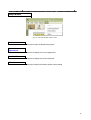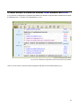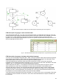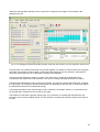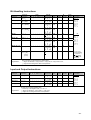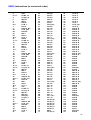
1
Deeds
Digital Electronics Education and Design Suite
User Manual
(Feb 2004)
Edited by Giuliano Donzellini and Domenico Ponta
1
Exegi monumentum aere perennius
regalique situ pyramidum altius
quod non imber edax, non Aquilo impotens
possit diruere, aut innumerabilis
annorum series et fuga temporum.
Quinto Orazio Flacco
2
Deeds - Digital Electronics Education and Design Suite
User Manual
Index
Preface
Introduction
P. 8
P. 9
Deeds as a learning environment for digital electronics
How to use Deeds to teach theory
How to use Deeds to solve exercises
How to use Deeds to learn to design electronic systems
The Deeds simulation tools
P. 10
P. 10
P. 10
P. 11
P. 12
Deeds: The Main Browser
Deeds: Main browser Menu
P. 13
P. 16
Deeds: The Assistant Browser (d-AsT)
Deeds: The Assistant Browser Menu
P. 22
P. 23
Deeds: The Digital Circuit Simulator d-DcS
Introduction
A simple example
A simple example of interaction between Deeds browsers and d-DcS
d-DcS: Menu Commands
P.
P.
P.
P.
P.
25
26
27
30
35
Deeds: Finite State Machine Simulator d-FsM
Introduction
Finite State Machines
FSM description languages: ASM charts
State Block
Decision Block
Conditional Output Block
ASM Charts & State Diagrams
FSM description languages: state transition table
FSM description languages: hardware description language
Learning FSM: methods and problems
Reusing FSM component: they can be imported in d-DcS
A simple example
A simple example of interaction between Deeds browsers and d-FsM
The timing diagram window
d-FsM: Menu Commands
P.
P.
P.
P.
P.
P.
P.
P.
P.
P.
P.
P.
P.
P.
P.
P.
48
49
50
50
51
51
51
51
53
53
55
55
56
60
67
68
Deeds: The Micro Computer Emulator d-McE
Introduction
A simple example
A simple example of interaction between Deeds browsers and d-McE
d-McE: Menu Commands
P.
P.
P.
P.
P.
77
78
80
84
91
3
DMC8 Instruction Set
Load Instructions (8 bits)
Load Instructions (16 bits) (first section)
Load Instructions (16 bits) (second section)
Arithmetic and Logic Instructions (8 bits)
Arithmetic Instructions (16 bits)
CPU Control Instructions
Jump Instructions
Call and Return Instructions
Rotate and Shift Instructions
Bit Handling Instructions
Input and Output Instructions
P. 100
P. 100
P. 101
P. 102
P. 103
P. 104
P. 104
P. 105
P. 105
P. 106
P. 107
P. 107
DMC8 Instructions (in alfabetical order)
P. 108
DMC8 Instructions (in numerical order)
P. 112
Appendix: Deeds historical version notes
P. 116
4
Index of Figures
Page #
Fig. 1: An example of laboratory report displayed in the main browser of Deeds
Fig. 2: The Deeds environment: the main and assistant browsers (on top left), and the three
Simulation Tools: the Digital Circuit Simulator (on top right), the Finite State Machine Simulator
(on bottom left) and the Micro Computer Emulator (on bottom right).
Fig. 3: The main browser of Deeds, showing the HTML page that allows to connect to the Deeds
web site and to the ‘on-line’ learning materials.
Fig. 4: The main browser, connected to the ‘Sreen Shots’ page of the Deeds web site.
Fig. 5: The download page in the Deeds web site.
Fig. 6: the learning material page (available in the Deeds web site), opened in the main
browser.
Fig. 7: The main browser “File“ menu.
Fig. 8: The Open Page dialog window.
Fig. 9: The main browser “Run“ menu.
Fig. 10: The main browser “Tools“ menu.
Fig. 11: The main browser “Options“ menu.
Fig. 12: The main browser “Help“ menu.
Fig. 13: The Assistant opened aside of the main browser, showing a page with a problem
assignment.
Fig. 14: The Assistant main menu, appended to the toolbar.
Fig. 16: The circuit editor of the Digital Circuit Simulator (d-DcS).
Fig. 17a: The drawing phase of the digital circuit editor: the insertion of components.
Fig. 17b: The next phase of the work: the connection of components, using wires
Fig. 17c: The animation at work: the user switches the Inputs and the circuit shows changes on
the Outputs.
Fig. 18: The Timing Diagram simulation window.
Fig. 19: The timing simulation results, displayed in the Timing Diagram window.
Fig. 20: A list of laboratory assignments, opened in the Deeds main browser.
Fig. 21: The specific laboratory assignment, opened in the Assistant browser.
Fig. 22: The Digital Circuit Simulator, opened by a click on the web page. The circuit template
has been automatically downloaded from the courseware site.
Fig. 23: The timing simulation of the circuit, once completed by the student.
Fig. 24: The student can download the report template to speed up its compilation and
delivering.
Fig. 25: The report template for this laboratory assignment.
Fig. 26a: The d-DcS “File“ menu.
Fig. 26b: The Paper Setup dialog window.
Fig. 27: The d-DcS “Edit“ menu.
Fig. 28: The d-DcS “View“ menu.
Fig. 29: The d-DcS “Tools“ menu.
Fig. 30: The d-DcS “Circuit“ menu.
Fig. 31: The d-DcS “Simulation“ menu.
Fig. 32: The d-DcS “Deeds“ menu.
Fig. 33: The d-DcS “Options“ menu.
Fig. 34: The d-DcS “Help“ menu.
Fig. 35: The ASM editor of the Finite State Machine Simulator (d-FsM).
Fig. 36: The ASM editor of the Finite State Machine Simulator (d-FsM).
Fig. 37: A simple Algorithmic State Machine (ASM) diagram.
Fig. 38a: State Block
Fig. 38b: Decision Block
Fig. 38c: Conditional Output Block
Fig. 39a: The State Diagram representation of a SR flip-flop.
Fig. 39b: The ASM Chart representation of a SR flip-flop.
Fig. 40a: ASM chart and State diagram representing the same algorithm: the FSM waits in the
state ‘a’ until the x input goes to one.
Fig. 40b: Another example of ASM chart and State diagram representing the same algorithm.
Fig. 41: The state transition table of the example above, as generated by the d-FsM.
Fig. 42: The VHDL equivalent of the ASM diagram in Fig. 37, as generated by the d-FsM.
11
12
13
14
14
15
16
16
18
19
20
21
22
23
26
27
27
28
28
29
30
31
32
32
33
34
35
36
37
38
39
40
44
45
46
47
49
50
50
51
51
51
51
52
52
53
53
54
5
Fig. 43: In this example, a component, designed with the d-FsM, has been imported in the
d-DcS.
Fig. 44a: The student inserts state blocks, setting their properties.
Fig. 44b: The student inserts conditional blocks, setting their properties.
Fig. 44c: The student inserts logical path (the green lines, no property needs to be set). Note
that the line arrows are automatically added.
Fig. 45: The simulation results for the edge detector described above.
Fig. 46a,b: The ASM transition table describing the component, on the left, and the generated
symbol, on the right.
Fig. 47: Two instances of the component are connected in a circuit composed of standard gates,
in the d-DcS.
Fig. 48: Timing simulation of the previous network, obtained with the d-DcS.
Fig. 49: A list of laboratory assignments, with use of d-FsM, opened in the Deeds main browser.
Fig. 50a: The specific laboratory assignment, opened in the Assistant browser (first page).
Fig. 50b: The specific laboratory assignment, opened in the Assistant browser (second page).
Fig. 51: The downloaded ASM diagram, template of the solution.
Fig. 52a,b,c: The three pages of the Input/Output dialog window, used to define inputs, outputs
and state variables .
Fig. 53: The property window, displaying the properties of the ‘a’ state.
Fig. 54: The property window, displaying the properties of a condition block.
Fig. 55: The finished ASM diagram, and its timing simulation, in the d-FsM.
Fig. 56: The finished d-DcS schematic, and the timing simulation of the component, in the dDcS.
Fig. 57: Also in this case, the student will download the report template to speed up its
compilation and delivering.
Fig. 58: The report template for this laboratory assignment assignment.
Fig. 59: The Timing Diagram window of the d-FsM.
Fig. 60: The ASM Table window.
Fig. 61: The d-FsM “File“ menu.
Fig. 62: The VHDL code window.
Fig. 63: The Paper Setup dialog window.
Fig. 64: The d-FsM “Edit“ menu.
Fig. 65: The three pages of the Input/Output dialog window, used to define inputs, outputs and
state variables .
Fig. 66: The d-FsM “View“ menu.
Fig. 67: The four pages of Property Window, used to define properties of state, conditional and
conditional output blocks.
Fig. 68: The d-FsM “Simulation“ menu.
Fig. 69: The d-FsM “Window“ menu.
Fig. 70: The d-FsM “Deeds“ menu.
Fig. 71: The d-FsM
Fig. 72: The assembler code editor of the Micro Computer Emulator (d-McE).
Fig. 73: The assembler-level debugger of the Micro Computer Emulator.
Fig. 74: The emulated board, as represented in the Micro Computer Emulator.
Fig. 75: The editing phase of an assembly program, in the d-McE.
Fig. 76: The DMC8 “architecture”, as shown by the help-system.
Fig. 77: An example of the ‘on line’ instruction set documentation: the Arithmetic and Logic
instructions.
Fig. 78: Another example of the ‘on line’ instruction set documentation: the Shift and Rotate
instructions.
Fig. 79: The Assembler module reports an error in the source code.
Fig. 80: The Debugger module shows the program under test, the memory, the CPU registers,
the I/O ports.
Fig. 81: A list of laboratory assignments, opened in the Deeds main browser.
Fig. 82a: The specific laboratory assignment, opened in the Assistant browser (first part).
Fig. 82b: The specific laboratory assignment, opened in the Assistant browser (second part).
Fig. 83: The Micro Computer Emulator, opened by a click on the web page. The editor shows
the trace of the solution, automatically downloaded from the courseware site.
Fig. 84: The program under test in the interactive debugger of the d-McE: a Warning has be sent
to the user.
Fig. 85: Port addresses can be modified in the “I/O Ports Address Decoding” dialog window.
Fig. 86: Port addresses can be modified by a mouse click on the simulated ‘on board’ dip
55
56
56
57
57
58
58
59
60
61
62
62
63
63
64
64
65
66
66
67
67
68
69
69
71
71
72
72
73
74
75
76
78
79
79
80
81
81
82
82
83
84
85
86
87
88
89
89
6
switches.
Fig. 87: The student can download the report template to speed up its compilation and
delivering.
Fig. 88: The simple template provided on the web page, that the student can download.
Fig. 89: A partial view of a ‘final’ student report.
Fig. 90: The d-McE “File“ menu.
Fig. 91: The d-McE “Edit“ menu.
Fig. 92: The d-McE “Project“ menu.
Fig. 93: The “Source Info” dialog window.
Fig. 94: The “I/O Ports Address Decoding” dialog window.
Fig. 95: The d-McE “Emulation“ menu.
Fig. 96: The d-McE “Deeds“ menu.
Fig. 97: The d-McE “Options“ menu.
Fig. 98: The d-McE “View“ menu.
Fig. 99: The Symbol Table window. (Compact View or Extended View).
Fig. 100: The d-McE “Help“ menu.
89
90
90
91
93
94
94
94
95
96
97
98
98
99
7
Preface
Deeds is the acronym of Digital Electronics Education and Design Suite… but, as ”deeds”
mean, I’m not sure if they will be good or bad… just like The Deeds of Gallant Knights that the splash form
recalls…
“The Deeds of Gallant Knights"
…from a picture of G. David, XVI Century - Paris, Musèe de l'Armèe
8
Deeds
Digital Electronics Education and Design Suite
Introduction
Deeds is conceived as a suite of simulators, tools and learning material for Digital Electronics. Deeds helps
student acquiring theoretical foundations, analysis capabilities, ability to solve problems all over the subject
topics, practical synthesis and design skills. Its approach is characterised by the "learning-by-doing” concept.
It covers the following areas of digital electronics:
• Combinational logic networks (from simple gates to decoders,
encoders, multiplexers and demultiplexers);
• Sequential logic networks (from simple flip-flops to registers and
counters);
• Finite state machine design;
• Micro-computer programming (at assembly level) and interfacing;
Major tools that Deeds includes are:
• An HTML main browser, to navigate in Internet, where students will
find lessons, exercises and laboratory assignments;
• An HTML assistant browser, that assists students in their work;
• A schematic digital circuit editor (with component data-sheet support);
• An interactive circuit ‘animator’ (to experiment with components and
simple networks directly on the schematics);
• An interactive logic simulator (with a timing diagram tracer to analyse
events in the logic networks, and to interact step-by-step with the
circuit);
• A finite state machine editor / simulator (the algorithm is described
using an Algorithmic State Machine graphical editor);
• A microcomputer board emulator (the board include an 8 bit CPU,
ROM, RAM, I/O ports);
• An assembler level / interactive debugger module.
Deeds tools can interact with each other:
• The HTML main and assistant browsers allows to launch all the other
tools and interact with them;
• The browser can control editors and simulators, to realise a true
interaction between text and experiments;
• The schematic editor allows to connect traditional logic circuits with
subsystems defined by the user with the help of the finite state
machine editors and the micro-computer emulator.
• It is possible to experiment with digital systems controlled by state
machines.
The architecture of Deeds allows a “scalable” approach to the lessons, exercises and laboratory sessions.
All the tools included allow either a simplified scenario to beginners and a more exhaustive and complete
environment for skilled students.
9
Deeds as a learning environment for digital electronics
Deeds is conceived as a learning environment for digital electronics. With such term we mean a collection
of tools and text material that help students acquiring:
•
•
•
•
theoretical foundations of the subject;
analysis capabilities;
ability to solve problems all over the subject topics;
practical synthesis and design skills.
Deeds is conceived as a common resource for all introductive courses in digital electronics. As such, it may
contain different technical subjects, different pedagogical formats (lectures, exercises, lab assignments,
etc.) delivered at different student levels. Deeds is therefore born as a set of tools (listed before) that
teachers can complete and personalise to suit their pedagogical needs by contributing to the ”lecture space”
with their own materials.
There is no need for a specific authoring tool, because the lecture space can be composed with any HTML
editor, completed by a helper application that facilitates the linking of the editors and simulators’ commands
to the lecture text.
How to use Deeds to teach theory
A “lecture” based on Deeds appears as HTML pages with text and figures. The page aspect and layout are
totally up to the author. At this level, students see a “normal” on-line book or document. But many of the
figures and visual objects are “active”, because they are connected to the editing and simulation tools of
Deeds.
For example, let’s suppose that theory presents a certain digital circuit , visualising its schematics in a
picture. When the user clicks on the picture, Deeds launches the corresponding simulator, and opens that
schematic, together with another windows (the Helper) that contains step-by-step instructions on how to
explore or test the circuit itself. Such procedure is equally useful to convey concepts on simple components
or quite complex networks. In the first case, simulators allows to “animate” circuits, i.e. to explore them
interactively. In the second one, their capabilities of tracing signals in the time and data domain allows a
thorough test of the network.
How to use Deeds to solve exercises
The target of traditional exercises is to help understanding theory, applying it to simple cases and providing a
feedback to the teacher through the delivery of the solutions. In our system exercises are presented as
HTML pages, containing text and figures of the assignments. The role of Deeds is to allow students to check
the correctness of the solutions obtained manually and to provide
graphical tools for editing the web page containing their reports,
until they are satisfied with their work and use Deeds to deliver the
reports through the network.
The use of Deeds implies also a different approach to the structure
of the exercises. In fact, with the simulator, students may be
tempted to skip manual analysis. Exercises, therefore, must be
targeted more to the real understanding of the issues than to the
execution of repetitive tasks.
10
How to use Deeds to learn to design electronic systems
The development of a digital design project is the field where Deeds can fully be exploited. In fact, the
interactive logic simulator, the finite state machine module and the microcomputer board emulator can work
simultaneously in the simulation of a system where standard digital components can be controlled by a state
machines as it is the case in contemporary digital design. Obviously, the modules can be used
independently, to test separately the system’s parts. The student can complete its work programming at
assembly level a microcomputer board.
Students use Deeds to download the assignment from a web page. The assignment consists of a functional
description and a set of specification of the system that students must design. The approach is meant to
replicate the features of a professional environment, within the guidelines suggested by the educational
purposes. Project development phases are guided by help and instructions supplied through the Assistant
Browser. Such instructions can be given step-by-step or by simple guidelines: the use of the simulation tools
can be more or less guided by the text of the assignment (to left creativity and fantasy to the user initiative).
In Fig. 1, an example of laboratory student report, displayed in the main browser.
Fig. 1: An example of laboratory report displayed in the main browser of Deeds
11
The Deeds simulation tools
The simulation tools are three: a Digital Circuit Simulator (d-DcS), a Finite State Machine Simulator (d-FsM),
and a Micro Computer Board Emulator (d-McE). All the simulation tools are characterized by a “learn-bydoing” approach. They are integrated together: design and simulation of complex networks integrating
standard logic with state machines are possible. In Fig. 2 a few screen shots of the Deeds tools are shown.
Fig. 2: The Deeds environment: the main and assistant browsers (on top left), and the three Simulation Tools:
the Digital Circuit Simulator (on top right), the Finite State Machine Simulator (on bottom left)
and the Micro Computer Emulator (on bottom right).
12
Deeds: The Main Browser
The simulators are integrated around two HTML browsers, enabling active Internet navigation to sites
where students find pages with lessons, exercises and laboratory assignments. The main web browser of
Deeds, when activated, shows a HTML page that allows to connect to the Deeds web site and to the ‘online’ learning materials developed at DIBE (University of Genoa).
The main browser (Fig. 3) has been developed around the standard Microsoft WebBrowser ® component,
the same used by the Microsoft Internet Explorer ®, extended to support all the required functions by the
Deeds environment. It is mainly used to connect to the sites containing the learning materials. The browser
supports all the features that the user can expect to find, including JAVA Virtual Machine ®, JavaScript ®,
VBScript ®, XML support.
Fig. 3: The main browser of Deeds, showing the HTML page that allows to connect to the Deeds web site and to the
‘on-line’ learning materials.
When the user launches the Deeds environment, the main browser shows up. All the other tools can be
activated by the menu and/or toolbar command. The main browser acts as ‘main window’ of the application
suite.
13
With Deeds, the user can directly navigate to the own web site, where Learning Material are available. In
Fig. 4 you see the ‘screen shots’ web page of the site.
Fig. 4: The main browser, connected to the ‘Sreen Shots’ page of the Deeds web site.
The user can also download the last version of the Deeds suite, as soon as it become available (Fig. 5):
Fig. 5: The download page in the Deeds web site.
14
Deeds has been developed as common simulation tool to be shared among different institutions running
courses on Digital Design, as a support of the activities of the NetPro project in the field of Electronic
Engineering. NetPro, a European project of the Leonardo DaVinci program, develops project-based
learning through Internet. It has created models, tools and services to facilitate communication and
collaboration between distant students, and to manage access and control of project deliverables.
We test NetPro methodologies and tools by running pilot projects. An important characteristic of the pilot
courses is that project groups can be distributed over different academic institutions and countries. A pilot
course may have teams from more than one institution and more than one nation while teams themselves
could be inter-institutional and international.
The immediate goal of the collaboration between pilot sites is to provide learning tasks that are meaningful
for all students, independently of their local arrangements.
Joint working is possible if teams use the same language (all the components of our pilots, including
student deliverables and communication, are in English) and if the classes involved study the same topic at
the same time of year. All documents produced are available as web sites for on-line fruition or as
downloadable files. In fig. 6 you see, opened in the main browser, the learning material index page,
available in the Deeds web site.
Fig. 6: the learning material page (available in the Deeds web site), opened in the main browser.
15
Deeds: Main browser Menu
The main browser menu allows to navigate web site, to run simulators and tools, to switch between the
opened tools, and to customize the user options.
File Menu
Fig. 7: The main browser “File“ menu.
Home Page
Command to navigate to the main browser home page (it can be user-defined)..
Open Page
Open the Open Page dialog (Fig. 8). In this dialog window, the user can type
directly a URL address, or browse the local network or disk. The chosen web page
can be set as Home Page. A short history of previously opened pages is
maintained.
Fig. 8: The Open Page dialog window.
16
Back
Standard browsing command to return to the ‘previous’ opened page.
Forward
Standard browsing command to return to the ‘next’ opened page, after using the
‘Back’ command.
Stop
Standard browsing command to stop the download of the current page.
Refresh
Standard browsing command to reload the currently opened page.
Print Preview
Standard command to preview the current page before printing.
Print Page
Standard command to print the current page.
Exit
Standard command to close the Assistant.
17
Run Menu
Fig. 9: The main browser “Run“ menu.
Assistant Browser
Command to open manually an instance of the Assistant Browser.
Digital Circuit
Simulator
Command to open manually an instance of the Digital Circuit Simulator (d-DcS).
Finite State
Machine Designer
Command to open manually an instance of the Finite State Machine
Designer/Simulator (d-FsM).
Micro Computer
Board Emulator
Command to open manually an instance of the Micro Computer Board Emulator
(d-McE).
18
Tools Menu
Fig. 10: The main browser “Tools“ menu.
First items group
Commands to switch focus to the chosen tool. All the opened tools are indexed
here, together with the name of the corresponding opened file, if any. When the
user click on an item, the tool will go ‘on top’.
Switch to Next
Deeds Application
Command to switch to the next Deeds open tool or browser.
Switch to
Tool on Top
Command to switch to the tool that was ‘on top’ before switching to the main
browser.
Close All Tool
Command to close all the opened tool. If a file, opened in a tool, is not saved, the
user will be prompted, and the close operation stopped.
19
Options Menu
Fig. 11: The main browser “Options“ menu.
Configuration
Command to change the application configuration (disabled in this version).
ToolBars
Commands to control ToolBars appearance.
Browser ToolBar
Command to hide or show the Browser ToolBar.
Status Bar
Command to hide or show the Status Bar.
Show and Dock
All ToolBars
Command to show and dock in all the ToolBars.
Dockable
ToolBars
Command to enable or disable the docking modality of the ToolBars.
20
Help Menu
Fig. 12: The main browser “Help“ menu.
Index
Command to open the Deeds Help System.
License
Agreement
Command to display the Licence Agreement.
Version Notes
Command to display the Version Notes file.
About
Command to display the Deeds ‘splash’ window dialog.
21
Deeds: The Assistant Browser (d-AsT)
The “Assistant” HTML browser has characteristics similar to those of the main browser, but it is specialized
to assist students, side by side, in their work (fig. 13). This is the browser used to open lessons, exercises
and laboratory assignments. As the main, also the Assistant browser has been conceived around the
standard Microsoft WebBrowser ® component.
In Fig. 13 the Assistant browser is opened aside of the main one, showing a page with a problem
assignment (from the ESD1 NetPro course). To open an assignment, the user will click on the desired
topic, listed in the main browser: the Assistant will open automatically, showing itself aside.
Fig. 13: The Assistant opened aside of the main browser, showing a page with a problem assignment.
All objects, that a web page visualises, can be made “active”. For instance, by clicking on the figure
showing the schematics, the Digital Circuit Simulator could be started and the circuit loaded, ready to be
tested (this important feature will be described in detail later).
22
Deeds: Assistant browser Menu
The Assistant menu has been reduced to the essential (Fig. 14), to simplify user operation. Its graphical
shape has been chosen to minimize the window size, allowing the positioning of the Assistant aside of the
simulation tool without occupy to much area of the screen.
Fig. 14: The Assistant main menu, appended to the toolbar.
Home Page
Command to navigate to the Assistant local home page.
Open Page
Open the Open Page dialog (Fig. 15). In this dialog window, the user can type
directly a URL address, or browse the local network or disk. The chosen web page
can be set as Home Page. A short history of previously opened pages is
maintained.
Fig. 15: The Open Page dialog window.
Back
Standard browsing command to return to the ‘previous’ opened page.
Forward
Standard browsing command to return to the ‘next’ opened page, after using the
‘Back’ command.
23
Stop
Standard browsing command to stop the download of the current page.
Refresh
Standard browsing command to reload the currently opened page.
Print Preview
Standard command to preview the current page before printing.
Print Page
Standard command to print the current page.
Deeds
Command group to navigate between the opened Deeds tools.
Options
Command group to change the Assistant configuration and options.
Exit
Standard command to close the Assistant.
24
Deeds: The Digital Circuit Simulator d-DcS
This image from the Tapestry of Bayeux, Bayeux Cathedral, France
25
Introduction
The Digital Circuit Simulator d-DcS appears to the user as a graphical schematic editor, with a library of
simplified logic components, specialised toward pedagogical needs and not describing specific commercial
products (Fig. 16).
As described before, the schematic editor allows to build simple digital networks composed of gates, flipflops, pre-defined combinational and sequential circuits and custom-defined components (defined as Finite
state machine).
Fig. 16: The circuit editor of the Digital Circuit Simulator (d-DcS).
Simulation can be interactive or in timing-mode. In the first mode, the student can "animate" the digital
system in the editor, controlling its inputs and observing the results. This is the simplest mode to examine a
digital network, and this way of operation can be useful for the beginners.
In the timing mode, the behaviour of the circuit can be analysed by a timing diagram window, in which the
user can define graphically an input signal sequence and observe the simulation results. This is the mode
nearest to the professional simulators.
26
A simple example
In following screen shots (Fig. 17a,b,c), you can see the circuit during the drawing and then simulated by
animation:
a) the student picks-up components from the bin on the Component Tool Bar, then
b) connects them using Wires. When finished,
c) the student activates the animation.
Fig. 17a: The drawing phase of the digital circuit editor: the insertion of components.
Fig. 17b: The next phase of the work: the connection of components, using wires
.
27
Fig. 17c: The animation at work: the user switches the Inputs and the circuit shows changes on the Outputs.
To enter the ‘animation’ mode, the user clicks on the triangular ‘play’ button
on the toolbar.
During the animation, the editing command are disabled, and the circuit can’t be changed; when the user
clicks on the Input Switches
showing ‘0’
, ‘1’
(see Fig. 17c), the Outputs change according to the simulation results,
or ‘unknown’
values.
To exit the ‘animation’ mode, it is necessary to click on the square ‘stop’ button
.
Instead, if the timing simulation is to be performed, the user should click on the Timing Simulation button
This will show the Timing Diagram simulation window (Fig. 18), very similar to the ones that we find in
professional tools for digital electronics.
.
Fig. 18: The Timing Diagram simulation window.
28
In this window, first of all the user defines the timing of the input signals, drawing them on the diagram with
the mouse. A vertical line cursor permits to define the ‘end time’ of the simulation. When the user clicks on
the triangular ‘play’ button
same window (Fig. 19).
on the toolbar, the simulation is executed, and its results are displayed in the
Fig. 19: The timing simulation results, displayed in the Timing Diagram window.
The student can verify the correct behaviour of the network under test, comparing simulation results with
reasoning and theory concepts.
29
A simple example of interaction between Deeds browsers and d-DcS
In Fig. 20 a list of assignments is opened in the Deeds main browser. Suppose that the student has to attend
the assignment # 2.1: “Analysis of a demultiplexer (1 to 2)”.
Fig. 20: A list of laboratory assignments, opened in the Deeds main browser.
Than, he or she clicks on the link, and the assignment will open in the Assistant (see Fig. 21).
30
Fig. 21: The specific laboratory assignment, opened in the Assistant browser.
The assignment asks the user to verify the behavior of the 1->2 demultiplexer represented in the figure,
using the Deeds Digital Circuit Simulator ). The text suggests to click on the figure to open in the d-DcS a
trace of the network's schematic, and then to complete it.
In this example, you see that it is necessary only a simple click on the figure to activate the simulator and to
download from the web site a ‘template’ of the solution. This approach aims to simplify user operation,
avoiding to spend time in no useful and distracting tasks.
31
The user will see the Digital Circuit Simulator, and the file downloaded in it, as in Fig. 22.
Fig. 22: The Digital Circuit Simulator, opened by a click on the web page. The circuit
template has been automatically downloaded from the courseware site.
The assignment suggests now to complete the drawing, and also to activate a few useful simulator
commands directly from the web page, with a simple click.
Once completed the schematic, also the simulation can be started, directly from the Deeds web page. In Fig.
23 you can see the results expected from the student work.
Fig. 23: The timing simulation of the circuit, once completed by the student.
32
Now is the time for the student to compile and deliver a good report. In the Deeds assignment page, a link is
prepared to download and edit a report template file (Fig. 24).
Fig. 24: The student can download the report template to speed up its compilation and delivering.
This has been previewed to uniform the report styles, making easier the teacher task, especially when the
number of student is valuable. But the availability of a report template is very useful also to the student,
because it saves a lot of time, speeding up the student work and leaving more time to concentrate on the
arguments to learn.
33
This is the report template for this laboratory assignment (Fig. 25).
Fig. 25: The report template for this laboratory assignment.
34
d-DcS: Menu Commands
The menu of the Digital Circuit Simulator allows the user to access all the function of the application. The
ToolBars replicate most of the commands already in the menu, to speed up user operations.
File Menu
Fig. 26a: The d-DcS “File“ menu.
New
Command to create a new circuit file.
Open
Command to open a circuit file. The file can be also downloaded directly from a
web site.
Save
Command to save current circuit file.
Save as
Command to save current circuit file with a different name or in a different position.
Print
Command to print the circuit.
35
Paper Setup
Command to define current paper format and orientation. It displays the Paper
Setup dialog window (Fig. 26b).
Fig. 26b: The Paper Setup dialog window.
Recent Files List
Commands to re-open the most recent files. Up to 8 recent files can be reopened
with this list. The symbol that is displayed on the left of the file name means that:
The file has been stored by the user on the local disk or network.
The file has been downloaded from a web site, but it has not been saved
(yet) on the local disk or network.
The file has been loaded from a local courseware, where it is read only
and it has not been saved (yet) on the local disk or network.
Exit
Standard command to close the application.
36
Edit Menu
Fig. 27: The d-DcS “Edit“ menu.
Undo
Command to undo the previous operation.
Redo
Command to redo the operation previously cancelled by the Undo command
(command temporary inhibited).
Cut
Command to cut the selected part of the circuit, and copy it on the clipboard
(command temporary inhibited).
Copy
Command to copy the selected part of the circuit on the clipboard (command
temporary inhibited).
Paste
Command to paste the clipboard content in the circuit (command temporary
inhibited).
Select All
Command to select all the object of the drawing.
Copy Image
Command to copy the selection as a bitmap image and put it on the Clipboard.
Delete
Command to delete all the selected components.
37
View Menu
Fig. 28: The d-DcS “View“ menu.
Zoom In
Command to “zoom in” the drawing.
Zoom Out
Command to “zoom out” the drawing.
Zoom 1,2,3,4,5
Command to “zoom” the view to different levels The “standard” level is the ‘3’.
Normal
Command to set the “normal view” of drawing space (i.e. as uniform continuous
background, only with the indication of drawing margins).
Page Layout
Command to set the view of the drawing space as a paper foil (i.e. with visible foil
borders and shadows, together with drawing margins).
38
Tools Menu
Fig. 29: The d-DcS “Tools“ menu.
Select One
Command to selects one object (by point and click).
Select by Area
Command to select a group of objects in a rectangular area.
Select and Move
Command to select and move a single object (by point and click).
Select and Delete
Command to select and delete a single object (by point and click).
Label
Command to insert (or edit) the label of a selected object (it is possible to associate
labels only to Input/Output blocks and to Finite State Machine components).
Rotate
Group of commands to rotate an object (during its insertion).
Right, Down
Left, Up
Four commands to rotate an object (during its insertion) to the specified direction.
Toggle
Command to toggle the direction of an object (during its insertion).
39
Circuit Menu
Fig. 30: The d-DcS “Circuit“ menu.
Clock Generator
Command to insert in the circuit a Clock Generator component.
Input
Command to insert in the circuit a Input Switch component.
High Level
Command to insert in the circuit a High Level Input component (logic ‘1’).
Low Level
Command to insert in the circuit a Low Level Input component (logic ‘0’).
Wire
Command to insert in the circuit a wire segment. The wiring system supports
automatic insertion of “wire nodes” when a wire is connected to another one.
40
Output
Command to insert in the circuit a binary Output Display component (it displays ‘0’,
‘1’ or ‘unknown’ symbols).
Display
Command to insert in the circuit an Hexadecimal Output Display component (it
displays hex digits from ‘0’ to ‘F’, or a ‘unknown’ symbol).
Input
Command to insert in the circuit a Input Switch component.
Error Check List
Command to error check the wiring of the circuit. It shows or hides, at the bottom of
the window, an “error check list” of wire connections.
Components
Command to insert in the circuit a component, selected by the user in the sub
menu. A description of all the sub menu’s is reported in the following.
Not
Command to insert a ‘NOT’ component.
ANDs
Commands to insert ‘AND’ components.
NANDs
Commands to insert ‘NAND’ components.
ORs
Commands to insert ‘OR’ components.
41
NORs
Commands to insert ‘NOR’ components.
EXORs
Commands to insert ‘EXOR’ and ‘EXOR tree’ components.
Decoders
Commands to insert ‘Decoder’ components.
Encoders
Commands to insert a ‘Priority Encoder’ component.
Multiplexers
Commands to insert ‘Multiplexer’ components.
Demultiplexers
Commands to insert ‘Demultiplexer’ components.
42
Flip-Flop
Commands to insert ‘Flip-Flop’ components.
Registers
Commands to insert ‘Register’ components.
Counters
Commands to insert ‘Counter’ components.
Finite State
Machine
Commands to insert ‘Finite State Machine’ components.
The ‘New’ command activate the Finite State Machine Simulator (d-FsM), allowing
the user to create a new component ‘from scratch’.
The ‘Load’ command allows the user to load a previously designed component.
43
Simulation Menu
Fig. 31: The d-DcS “Simulation“ menu.
Mode
Command group to set the simulation mode.
Interactive
Animation
Command to set the Interactive Animation Mode for simulation. When activated,
simulation don’t start immediately. If the Timing Diagram window is opened, it will
be closed. The editing commands are disabled, and the user is prompted to save
the file in the schematic editor, if it is not.
Timing Diagram
Simulation
Command to set the Timing Diagram Mode for simulation. When activated,
simulation doesn’t start immediately, but the Timing Diagram window is opened
instead. The editing commands are disabled and the user is prompted to save the
file in the schematic editor, if it is not.
Start Animation
Command to start simulation, when currently mode is ‘Animation’.
Stop Animation
Command to stop simulation, when currently mode is ‘Animation’.
44
Deeds Menu
Fig. 32: The d-DcS “Deeds“ menu.
Switch to Deeds
Command to switch focus to the Deeds main browser.
Switch to Last
Command to switch to the tool that was ‘last on top’ before switching to the
currently opened instance of the d-DcS.
Switch to Next
Command to switch focus among all active Deeds applications, in order of
activation.
45
Options Menu
Fig. 33: The d-DcS “Options“ menu.
Configuration
Command to change the application configuration (disabled in this version).
ToolBars
Commands to control ToolBars appearance.
Standard ToolBar
Command to hide or show the Standard ToolBar (the upper one).
Component
ToolBar
Command to hide or show the Component ToolBar (the lower one).
Show and Dock
All ToolBars
Command to show and dock in all the ToolBars.
Dockable
ToolBars
Command to enable or disable the docking modality of the ToolBars.
Status Bar
Command to hide or show the Status Bar.
46
Help Menu
Fig. 34: The d-DcS “Help“ menu.
Index
Command to open the d-DcS Help System (disabled in this version).
Data sheets
Command to open the Data Sheets help system (disabled in this version).
License
Agreement
Command to display the Licence Agreement.
Version Notes
Command to display the Deeds “Version Notes” file.
About
Command to display the d-Dcs ‘splash’ window dialog.
47
Deeds: Finite State Machine Simulator d-FsM
This image from the Tapestry of Bayeux, Bayeux Cathedral, France
48
Introduction
The Finite State Machine Simulator d-FsM allows graphical editing and simulation of Finite State
Machines components, using the ASM (Algorithmic State Machine) paradigm (fig. 35). The tool allows the
local functional simulation of the finite state machines designed by the user, with runtime display of the
relations between state and timing evolution (fig. 36).
Fig. 35: The ASM editor of the Finite State Machine Simulator (d-FsM).
The components that the d-FsM produces can be directly used in the d-DcS and inserted into any digital
circuit. Also, it can be exported in VHDL language.
A general purpose Finite State Machine software simulator helps the student to enhance his design skills
and facilitates also the transition from the pedagogical to the professional field, by introducing CAD
methodologies.
49
Fig. 36: The ASM editor of the Finite State Machine Simulator (d-FsM).
Finite State Machines
Finite State Machines (FSM) represent a model to design a class of digital
sequential circuits. A sequential system is a block whose outputs are a
function not only of the current inputs but also of the previous ones. In other
words, the logic has a sort of “memory” which records previous input
history so it can be responded to in the present.
Given this definition, sequential circuits would seem to require enormous
amounts of memory to record all previous inputs. However, for any real
logic design task, the fact that previous input combinations result in only a
finite number of distinct output classes reduces this memory requirement to
manageable levels. This class of design is called a Finite State Machine, or
just a state machine.
Modern digital circuit design is essentially based on Finite State Machines.
Design, synthesis and documentation of a state machine require a formal
approach. Currently, several design methods are employed, based either
on graphic, tabular or textual representations of the algorithm underlying
the state machine.
FSM description languages: ASM charts
The most common graphical methods currently in use to describe a FSM
are Moore and Mealy State Diagrams. In our simulator we use the ASM
(Algorithmic State Machine) method, instead.
A typical ASM chart (or diagram) resembles flowchart notation (Fig. 37),
even if they are not the same thing. It describes state flow, the output
functions and the next-state functions of a state machine. ASM charts have
the same function as Moore and Mealy State Diagrams: they describe the
behaviour of finite state machines so that it is clearly understandable for the
designer and, at the same time, ASM charts support a direct translation into
a hardware realization of the control algorithm.
Fig. 37: A simple Algorithmic
State Machine (ASM) diagram.
50
An ASM chart is composed of three basic elements, the State (rectangular box), the Decision Block
(diamond) and the Conditional Output Box.
A set composed of one state box, decision blocks and conditional output blocks is named ASM Block. An
ASM Block has one entry point, but may have any number of exit paths, each of them connecting to another
state box.
The FSM moves from state to state at each clock cycle; each state may have a state output; conditional
blocks allow choosing a direction as a function of the value of the inputs; conditional outputs depend not only
on states but also on input values.
State Block
On an ASM chart, a state is represented by a state box, which is a rectangle
with the name of the state encircled and placed at the side of the rectangle
(Fig. 38a). You can specify that an output signal is unconditionally active in a
particular state by writing the output signal's name inside the corresponding
state box. Output signals written inside state boxes are known as state outputs
or Moore outputs.
Fig. 38a: State Block
Decision Block
While unconditional transitions can be represented with a straight, not labelled
arrow traced between two state boxes, conditional transitions deserve a more
specific symbol. This is called decision diamond. Depending on the value of the
expression written inside the diamond, the machine will follow one of the two
labelled transition arrows going out of the diamond. A diamond has always two
outgoing arrows, one labelled "1" (or TRUE) and the other labelled "0" (or
FALSE) that corresponds to the values of the boolean expression inside.
Fig. 38b: Decision Block
Conditional Output Block
Sometimes you may need to activate an output signal in a particular state only
if a certain condition on inputs is satisfied (such output signals are known as
conditional outputs or Mealy outputs). In that case you need to use the
conditional output block.
Just put the ellipse on a transition arrow coming out of a decision diamond, and
write inside the ellipse the name of the output signal you want to activate when
the expression inside the diamond is true. Please notice that the conditional
block does not represent a state; instead it activates an output that it is active
in the state it descends from.
Fig. 38c: Conditional Output
Block
ASM Charts & State Diagrams
It is easy to convert a State Diagram in an ASM Chart, and vice versa. In Fig. 39a we report a basic example
of State Diagram:
Fig. 39a: The State Diagram representation of a SR flip-flop.
51
The following ASM Chart (Fig. 39b) can be used to model exactly the same behaviour:
Fig. 39b: The ASM Chart representation of a SR flip-flop.
The first thing you can see is that in both models you have an object to represent the states of the machine.
The states are numbered (1, 2) in the State Diagram and labelled with letters (a, b) in the ASM Chart, but the
1:1 relationship between them is obvious:
•
•
state 1 = state a = flip-flop output "0"
state 2 = state b = flip-flop output "1"
Another noticeable thing is that the two models are morphologically very similar. In both models you can
observe that every state has two outgoing transitions, one being a loop on the state itself, and the other
going to the other state. This similarity is always true if you make a conversion between ASM Charts and
State Diagrams, just remember that in ASM Charts conditional transitions come out of decision diamonds
which are not states (but they "belong" to the state they descend from).
The method used to represent conditional transitions on ASM Charts is more algorithm-oriented, as it uses
flow-chart syntax, which is less redundant than State Diagram syntax. In this case, for example, it helps the
reader understand that the transition that follows state a depends only on the value of the S input. Similar
considerations can be done about the transition that follows state b: only the value of the R input is relevant
in that case.
The following pictures are examples of ASM Chart <-> State Diagram conversion (Fig. 40a and 40b).
Fig. 40a: ASM chart and State diagram representing the same algorithm:
the FSM waits in the state ‘a’ until the x input goes to one.
52
Fig. 40b: Another example of ASM chart and State diagram representing the same algorithm.
FSM description languages: state transition table
The state transition table (Fig. 41) is the most compact description of a FSM and lends itself very well to be
used as interface with computer software and as a basis for the logical synthesis of the hardware. Of course,
the table is not a valid FSM design tool because it does not provide any help in conceiving the FSM
algorithm. Its main usefulness rests therefore in its use as a synthetic representation that may be common to
both the languages described above.
Fig. 41: The state transition table of the example above, as generated by the d-FsM.
FSM description languages: hardware description language
The use of circuit description languages (HDL, VHDL, Verilog) to represent finite state machine has gained a
strong diffusion and probably in many cases has replaced the graphical languages. The description of the
state machine takes in this case the format of a high level software program.
The Finite State Machine Simulator exports the FSM components in VHDL format (Very High speed
integrated circuits Hardware Description Language). In Fig. 42 you can see the VHDL equivalent of the ASM
diagram in Fig. 37, as generated by the Finite State Machine Simulator.
The list starts with the “Entity” i.e. the definition of the FSM as a block with inputs and outputs. Then an
object (Architecture) of the entity is instantiated. An entity may be described in three different ways:
structural, data flow, functional. The structural description decomposes the entity in terms of basic digital
components and their connections. The data flow description represents the FSM in terms of signals and
operations on them. The last description, the functional one, is the more powerful because it allows to see
the hardware circuit as a software program with input and output variables.
The FSM is therefore described as a process activated, in our case, by the clock or reset signals. Each state
is coded as an internal variable. An instruction “case” within each state defines the outputs to activate and
the next state.
53
------------------------------------------------------------- DEEDS (Digital Electronics Education and Design Suite)
-- VHDL Code generated
-by Finite State Machine Simulator (d-FsM)
-- Copyright © 2001-2004 DIBE, University of Genoa, Italy
-Web Site: http://esng.dibe.unige.it/netpro/Deeds
-----------------------------------------------------------LIBRARY ieee;
USE ieee.std_logic_1164.ALL;
ENTITY Deriv_UC IS
PORT( ------------------------>Clock & Reset:
Ck:
IN std_logic;
Reset: IN std_logic;
------------------------>Inputs:
IIN:
IN std_logic;
------------------------>Outputs:
OOUT: OUT std_logic );
END Deriv_UC;
ARCHITECTURE behave OF Deriv_UC IS
-- (Behavioral Description)
TYPE states is ( state_a,
state_b );
SIGNAL State,
Next_State: states;
BEGIN
-- Next State Combinational Logic ---------------------------------FSM: process( State, IIN )
begin
CASE State IS
when state_a =>
if (IIN = '1') then
Next_State <= state_b;
else
Next_State <= state_a;
end if;
when state_b =>
if (IIN = '1') then
Next_State <= state_b;
else
Next_State <= state_a;
end if;
END case;
end process;
-- State Register -------------------------------------------------REG: process( Ck, Reset )
begin
if (Reset = '0') then
State <= state_a;
elsif rising_edge(Ck) then
State <= Next_State;
end if;
end process;
-- Outputs Combinational Logic ----------------------------------OUTPUTS: process( State, IIN )
begin
-- Set output defaults:
OOUT <= '0';
-- Set output as function of current state and input:
CASE State IS
when state_a =>
if (IIN = '1') then
OOUT <= '1';
end if;
when state_b =>
if (IIN = '0') then
OOUT <= '1';
end if;
END case;
end process;
END behave;
Fig. 42: The VHDL equivalent of the ASM diagram in Fig. 37, as generated by the d-FsM.
54
Learning FSM: methods and problems
The choice of a FSM description language is very important under the pedagogical point of view. When first
introducing the state machine, we believe it is essential that the learner masters its fundamental concepts
and develop an intuitive understanding of its behaviour. At this level, therefore we believe it is convenient to
represent the machine algorithms with graphical methods, in our case ASM charts.
When the student has gained familiarity with the design method and is ready to develop non-standard digital
structures described by a set of specifications, switching to an hardware description language will develop
his abstraction skills and introduce him to professional design.
The VHDL export feature has been developed to make easier the transition from ASM description method to
the HDL-based world.
Reusing FSM component: they can be imported in d-DcS
As said before, the component the d-FsM produces can be directly used in the d-DcS and inserted into any
digital circuit. In Fig. 43 you see a screen shot where the simple component (seen before) is imported in the
d-DcS, and the network is simulated.
Fig. 43: In this example, a component, designed with the d-FsM, has been imported in the d-DcS.
In the d-DcS the FSM interpreter works together the simulator kernel to produce functional results. FSM to a
maximum number of 64 states can be designed and simulated, and a practical limitation to 8 inputs and 8
outputs has been introduced, mostly for graphical reasons. Such limitations are largely compatible with the
learning aims of the simulator. The FSM interpreter is able to simulate synchronous FSM with conditioned
outputs.
In the d-DcS the student can drive the inputs and observe the outputs of the FSM block as well as the
internal state of the FSM (in Fig. 43, the row named with the name of the component: ‘deriv.fsm’).
The user can connect standard digital components to the FSM block and therefore simulate digital systems
characterised by a functional division between architecture and controller, the last one being implemented by
a finite state machine.
If a student wishes to compare the results with the ones obtained by traditional synthesis, he can proceed
manually using the table of transitions or the ASM chart in order to obtain a traditional structure with a state
register made by flip-flops and a combinational network based on logic gates.
55
A simple example
In following screen shots of the d-FsM (Fig. 44a,b,c), you can see the drawing of an ASM diagram, followed
by a preliminary verification in the internal timing simulator.
d) the student picks-up state blocks from the bin on the Tool Bar (Fig. 44a), then
e) adds conditional blocks (Fig. 44b) and, by last,
f) connect logically them using lines (Fig. 44c).
At every step, when needed, the student sets properties of each introduced block.
Fig. 44a: The student inserts state blocks, setting their properties.
Fig. 44b: The student inserts conditional blocks, setting their properties.
56
Fig. 44c: The student inserts logical path (the green lines, no property needs to be set).
Note that the line arrows are automatically added.
The diagram describes an edge detector. Each time the input ‘IN’ presents a transition (‘0’ to ‘1’, or ‘1’ to ‘0’),
an output pulse, of the duration of one clock cycle, is generated.
To verify its behaviour, it is possible simulate it with the d-FsM. The timing simulation of the d-FsM is only
functional: it don’t take in count component delays, for instance, because it simulates directly the algorithm,
without synthesize the network in term of gates and flip-flops. Fig. 45 shows the results of the simulation. As
expected, the output line OUT goes ‘high’ for one clock cycle each time the input line IN presents a level
transition.
Fig. 45: The simulation results for the edge detector described above.
57
In Fig. 46 is reported the ASM transition table describing the designed FSM, as well as the preview of the
automatically generated symbol of the new component.
Fig. 46: The ASM transition table describing the component, on the left, and the generated symbol, on the right.
Now the component is ready to be imported in the d-DcS. We insert the component in a very simple way,
loading it from file. An example of use of this component in the d-DcS is shown in the Fig. 47, where two
instances of it are connected in a circuit composed also of standard gates.
Fig. 47: Two instances of the component are connected in a circuit composed of standard gates, in the d-DcS.
58
Then the student could verify the correct behaviour of the network under test, comparing d-DcS simulation
results with those expected, in particular with the functional simulation produced by the d-Fsm. In Fig. 48,
you see a screen shot of the timing simulation obtained with the d-DcS.
Fig. 48: Timing simulation of the previous network, obtained with the d-DcS.
This image from the Tapestry of Bayeux, Bayeux Cathedral, France
59
A simple example of interaction between Deeds browsers and d-FsM
As in the example applied to the Deeds with the d-DcS, in Fig. 49 a list of laboratory assignments is opened
in the Deeds main browser.
Fig. 49: A list of laboratory assignments, with use of d-FsM, opened in the Deeds main browser.
The student executes the assignment # 8.1: “Design of a synchronous mod-5 up/down counter”. As in the
example related to the d-DcS, with a click of the user on the link, the specific assignment will be opened in
the Assistant (Fig. 50a and 50b).
60
Fig. 50a: The specific laboratory assignment, opened in the Assistant browser (first page).
The assignment asks the user to design a synchronous mod-5 up/down counter, using the Finite State
Machine Simulator.
In the laboratory assignment (Fig. 50a) is explained that the counter should generate a numerical sequence
on the outputs QC, QB and QA, depending from the line input EN and DIR. The counter is synchronous with
the clock CK and it is initialized by an asynchronous Reset input. In particular, the input DIR defines the
count direction (up or down), and the input EN enables the count operation, that will take place on every
clock positive edge.
61
In Fig. 50b, the assignment continues with a suggestion: to download an ASM diagram template, to be
guided toward the solution. If the student use this option, he or she could concentrate better on the
argument, instead of build from scratch the solution, bothering with the simulator details and spending time in
less useful and distracting tasks. The option is not mandatory, however, and the student can freely activate
the simulator without using the template.
Fig. 50b: The specific laboratory assignment, opened in the Assistant browser (second page).
To download the template, it is necessary only a simple click on the link in the text. The d-FsM will be
activated, and the file downloaded from the web site, automatically. In Fig. 51 you see the suggested
template, as downloaded in the simulator.
Fig. 51: The downloaded ASM diagram, template of the solution.
In the template, as the text of the assignment explains, the student will find some important definition already
set: the state variables X,Y,Z, the outputs QC, QB, QA and the inputs DIR and EN. The necessary five state
blocks are already drawn.
62
In Fig. 52a,b,c are displayed the pre-defined properties, as they appear in the Input/Output dialog windows,
that the user activates with the tool bar command
.
Fig. 52a,b,c: The three pages of the Input/Output dialog window, used to define inputs, outputs and state variables .
Note that the specification requires that the 'a' state will be the 'Reset' state, i.e. the 'starting' state of the
component at the activation of the asynchronous !Reset. Also this characteristic has been pre-defined in the
template, as the ‘a’ state appears in the drawing with a little diamond placed on it.
Actually, all the states properties have been pre-defined in the template. The user can modify this properties
opening the Property Window. This can be left aside to the editor, during the operations (to open it, press the
). In Fig. 53 you see the Property Window, as it appears when the user select the ‘a’ state
tool bar button
block (with a mouse click on it).
Fig. 53: The property window, displaying the properties of the ‘a’ state.
For a state block, the user can set or change the symbolic name (‘a’ in the present case), the state code
(‘000’, here), and the active outputs (none, in the example). The check box on the left imposes this one as
‘Reset State’.
The user is asked to complete the ASM diagram and, using the timing simulation integrated in the d-FsM, to
verify the correct sequence of output values and state codes. The user will start drawing, adding path lines
and diamonds, as required by the requested functionality.
63
In Fig. 54 you see the Property Window, as it appears when the user select a condition block. The user can
change the orientation of the diamond connections and the condition, chosen among the input variables
(‘DIR’ in this example).
Fig. 54: The property window, displaying the properties of a condition block.
Once the student have finished the design, the next step required is to verify the behaviour of the counter
with the timing simulator of the d-FsM itself (Fig. 55).
Fig. 55: The finished ASM diagram, and its timing simulation, in the d-FsM.
64
When the user clicks on the ‘Clock’ button, the internal simulator evaluates next state and outputs (according
to the current input values) and displays the results on the time diagram.
At the same time, in the editor window, the corresponding new state is highlighted (with a coloured frame
around it, see Fig. 55). This is an important feature, because a major difficulty, for a beginner, is to
understand the correspondence between states and events time sequence.
Finally, when the behaviour of the component satisfies all the required specifications, the component could
be imported in the d-DcS (see the assignment, Fig. 50b). Also in this case, a simple d-DcS schematic
template is provided, to speed up the operations; it can be easy downloaded and opened in the d-DcS with a
click on the hyperlink in the text. Once completed the schematic, the simulation of the counter could be
repeated in the d-DcS timing simulator (Fig. 56).
Fig. 56: The finished d-DcS schematic, and the timing simulation of the component, in the d-DcS.
As in the example related to the d-DcS, at this point the student will compile and deliver a report about its
work. As already seen, in the assignments page, a link is set to download a report template file (Fig. 57).
65
Fig. 57: Also in this case, the student will download the report template to speed up its compilation and delivering.
In Fig. 58 is displayed the report template prepared for this laboratory assignment, downloaded and ready to
be edited.
Fig. 58: The report template for this laboratory assignment assignment.
66
The timing diagram window
In this window (Fig. 59) the timing diagram of all the signals is constructed, during the simulation, in a
interactive mode. The timing diagram displays the Input and Output signals and, at bottom, the current State,
by symbolic name and by code.
Fig. 59: The Timing Diagram window of the d-FsM.
In the default mode, the user clicks on the ‘Clock’ button
clock cycle).
If the tool bar button
to advance the simulation by one step (a
is checked, the simulation step is automated (the execution speed is controlled by
the tool bar cursor
).
To toggle Input signal values, the user clicks on the Input signal buttons, under the ‘Clock’ button. In the
example of Fig. 59, the button is
The button
.
restarts simulation (from time = 0).
activates the ASM Table window (Fig. 60). In this table Inputs, Outputs and current and next
The button
States are expressed in a compact, tabular form.
Fig. 60: The ASM Table window.
67
d-FsM: Menu Commands
The menu of the Finite State Machine Simulator allows the user to access all the function of the
application. The ToolBars replicate most of the commands already in the menu, to speed up user
operations.
File Menu
Fig. 61: The d-FsM “File“ menu.
New
Command to create a new Finite State Machine file.
Open
Command to open a Finite State Machine file. The file can be also downloaded
directly from a web site.
Save
Command to save current Finite State Machine file.
Save as
Command to save current Finite State Machine file with a different name or in a
different position.
68
Close
Command to close the current Finite State Machine.
Export VHDL
Command to export the Finite State Machine ASM diagram in VHDL language. It
shows a window with the equivalent VHDL code, generated from the internal data
base (Fig. 62).
Fig. 62: The VHDL code window.
If you wish to save the generated code in a file, click on the ‘Save’ button: you will
prompted to chose a name file, before to save it. If you want include the VHDL
code in another text file, click on the ‘Copy’ button to pass all the VDHL code onto
the ‘clipboard’, ready to be pasted in a code editor of your choice.
Print
Command to print the Finite State Machine ASM diagram.
Paper Setup
Command to define current paper format and orientation. It displays the Paper
Setup dialog window (Fig. 63).
Fig. 63: The Paper Setup dialog window.
69
Recent Files List
Commands to re-open the most recent files. Up to 8 recent files can be reopened
with this list. The symbol that is displayed on the left of the file name means that:
The file has been stored by the user on the local disk or network.
The file has been downloaded from a web site, but it has not been saved
(yet) on the local disk or network.
The file has been loaded from a local courseware, where it is read only
and it has not been saved (yet) on the local disk or network.
Exit
Standard command to close the application.
70
Edit Menu
Fig. 64: The d-FsM “Edit“ menu.
Undo
Command to undo the previous operation (command temporary inhibited).
Cut
Command to cut the selected part of the ASM diagram, and copy it on the
clipboard (command temporary inhibited).
Copy Image
Command to copy the selection as a bitmap image and put it on the Clipboard.
Paste
Command to paste the clipboard content in the circuit (command temporary
inhibited).
Select All
Command to select all the object of the drawing.
Define In / Out
Command to define or modify Inputs, Outputs and State Variables. It activates a
modal dialog window (see Fig. 65), where the user can add, rename and delete the
Input and Output lines (up to 8 lines), as well as the State Variables (up to 6). The
dialog is divided in the specialized pages (Input, Output and State Vars).
Fig. 65: The three pages of the Input/Output dialog window, used to define inputs, outputs and state variables .
71
View Menu
Fig. 66: The d-FsM “View“ menu.
Zoom In, Out
Command to “zoom in” or “zoom out” the drawing.
Property ToolBox
Command to activate the “Property Window”, that enables the user to set and
modify the properties of the selected State Block, Conditional Block or Conditional
Output Block. It shows four different “property pages”, depending on the context
(Fig. 67).
Fig. 67: The four pages of Property Window, used to define properties of state, conditional and conditional output blocks.
Normal
Command to set the “normal view” of drawing space (i.e. as uniform continuous
background, only with the indication of drawing margins).
Page Layout
Command to set the view of the drawing space as a paper foil (i.e. with visible foil
borders and shadows, together with drawing margins).
72
Tools Menu
Fig. 68: The d-FsM “Simulation“ menu.
Start Simulation
Command to start the functional simulation of the finite state machine represented
by the currently ASM diagram. During simulation, the editor commands are
inhibited, and the “Timing Diagram” window is displayed (Fig. 59).
Stop Simulation
Command to stop simulation and return to the edit mode of the ASM diagram.
Four commands to rotate an object (during its insertion) to the specified direction.
73
Window Menu
Fig. 69: The d-FsM “Window“ menu.
Tile Vertical
Command to tile vertically the opened windows (the graphical editor, the timing
diagram, the ASM table).
Tile Horizontal
Command to tile horizontally the opened windows (as above).
Cascade
Command to cascade diagonally the opened windows (as above).
Arrange Icons
Command to reorder the icons of the iconized windows, at the bottom of the main
window.
Opened windows
list
Command to switch focus among the opened windows within the main window.
74
Deeds Menu
Fig. 70: The d-FsM “Deeds“ menu.
Switch to Deeds
Command to switch focus to the Deeds main browser.
Switch to Last
Command to switch to the tool that was ‘last on top’ before switching to the
currently opened instance of the d-DcS.
Switch to Next
Command to switch focus among all active Deeds applications, in order of
activation.
75
Help Menu
Fig. 71: The d-FsM “Help“ menu.
Index
Command to open the d-FsM Help System (disabled in this version).
License
Agreement
Command to display the Licence Agreement.
Version Notes
Command to display the Deeds “Version Notes” file.
About
Command to display the d-FsM ‘splash’ window dialog.
76
Deeds: The Micro Computer Emulator d-McE
This image from the ancient (and mysterious) Piri Reis map (1513)
77
Introduction
With the Micro Computer Emulator d-McE, the user can practice programming at assembly language level
(Fig. 72). It functionally emulates a board including a CPU, ROM and RAM memory, parallel I/O ports, reset
circuitry and a simple interrupt logic. The custom 8 bit CPU, named DMC8, has been designed to suite our
educational needs, and it is based on a simplified version of the well-known ‘Z80-CPU’ processor.
Fig. 72: The assembler code editor of the Micro Computer Emulator (d-McE).
The integrated source code editor enables user to enter assembly programs, and a simple command permits
to assemble, link and load them in the emulated system memory.
78
The execution of the programs can be run step by step in the interactive debugger (Fig. 73). In the debugger,
as in professional tools, the user can evaluate the contents of all the structures involved in the hardware /
software system, by stepping the execution of the programs.
Fig. 73: The assembler-level debugger of the Micro Computer Emulator.
Fig. 74: The emulated board, as represented in the Micro Computer Emulator.
79
A simple example
In the following screen shot (Fig. 75) you can see an assembly program edited in the d-McE code editor. The
code editor supports syntax highlighting. The code of the DMC8 microprocessor assembly is mainly the
same of the well-known ‘Z80-CPU’ processor, but reduced of some instructions, to simplify and ‘linearize’ the
instruction set.
Fig. 75: The editing phase of an assembly program, in the d-McE.
The microprocessor architecture is documented in the help system. This presents topics to the user as a
“multi-page” window (Fig. 76).
The instruction set is documented ‘on line’, to help the user in writing the assembly programs (examples in
Fig. 77 and 78).
80
Fig. 76: The DMC8 “architecture”, as shown by the help-system.
Fig. 77: An example of the ‘on line’ instruction set documentation: the Arithmetic and Logic instructions.
81
Fig. 78: Another example of the ‘on line’ instruction set documentation: the Shift and Rotate instructions.
When the user wishes to verify the correctness of the written code, or when the coding is finished, he or she
. In Fig. 79 an example of assembling report,
can launch the Assembler module, using the tool bar button
in case of error, is shown (a unknown label was found, and the offending line is pointed by a little symbol).
Fig. 79: The Assembler module reports an error in the source code.
82
When the code has been cleaned, and no syntax error is reported, the program can be tested in the
debugger (Fig. 80).
Fig. 80: The Debugger module shows the program under test, the memory, the CPU registers, the I/O ports.
The first ‘pane’ in the window shows the CPU internal registers. For instance, at this moment of the program
execution, the Program Counter register contains the value 003Ah (as you can see also in the last pane,
where the current instruction to be executed in actually at this address).
The second pane displays the memory contents. The used memory locations are highlighted: they
correspond to the object code under execution. The user can change manually each memory location.
The third pane represents the Input / Output port contents. The user can interact with these ports, changing
the Input values, by clicking on the little round buttons (corresponding to the port bits), or writing the value in
the field aside (in decimal or hexadecimal coding).
The last pane presents to the user the object code in execution, as loaded in memory, in numerical format
(on the left) and in assembly source format (on the right).
The student can execute the program step by step, or by animation, a modality that resembles the real
execution, but at ‘human readable’ speed. A cursor permits to regulate the animation speed to the needs of
the test.
83
A simple example of interaction between Deeds browsers and d-McE
In Fig. 81 a list of laboratory assignments is opened in the Deeds main browser. The student has to attend
the assignment # 4.1 of the course on Microcomputer: “Asynchronous serial communication”.
Fig. 81: A list of laboratory assignments, opened in the Deeds main browser.
With a click on the link, the assignment will open in the Assistant (see Fig. 82a and 82b).
84
Fig. 82a: The specific laboratory assignment, opened in the Assistant browser (first part).
In this assignment (Fig. 82a), we require to the student to write a program to receive and retransmit serial
asynchronous information, using the parallel ports available in the d-McE. The program should take in
charge the operation of de-serializing and serializing data. Also a simple cryptographic method is applied to
data before retransmitting it.
In the assignment is described the format of the serial data packet (standard 8 bit asynchronous serial
communication, without parity control). That protocol previews one start bit at ‘1’, eight data bits b7..b0 (b7
ahead), one stop bit at ‘0’. It is defined a low bit rate (100 bits per second), with the aim to let the user
concentrate on the basic tasks, without bothering too attention to timing problems.
The text continues suggesting to connect the input and output serial lines to specific bits of the available
input and output ports (INPORT and OUTPORT ).
The simple cryptographic operation requires that the program remember the previous transmitted byte and
combine it in a byte-wise EXOR operation with the currently received one.
85
Fig. 82b: The specific laboratory assignment, opened in the Assistant browser (second part).
The theme continue with the guidelines for a possible solution, as the student, at the moment of this
laboratory session, faces this kind of problems for the first time (Fig. 82b).
The Deeds let to get a trace of the solution, with a simple click on the specific link. It will be automatically
downloaded and opened in the source code editor of the d-McE (Fig. 83). As usual, this approach let the
user simplify the operations necessary to start with the ‘true’ work.
86
Fig. 83: The Micro Computer Emulator, opened by a click on the web page. The editor
shows the trace of the solution, automatically downloaded from the courseware site.
Note the icon visible on top of the editor page:
. In this case the symbol indicates that the file has been
downloaded from the web. When the user will save it on the local disk, this little icon will change in
.
Once completed the assembly coding of the program, the student will compile it. If no syntax error has been
found, the verification of the program functionality can start (Fig. 84).
87
Fig. 84: The program under test in the interactive debugger of the d-McE: a Warning has be sent to the user.
In Fig. 84 the program is ‘Animated’ by the student, i.e. it is automatically executed step by step, at a ‘human
readable’ speed. The speed is controlled by the cursor visible on the tool bar (“Animation Speed”).
In this example, a typical warning message is generated by the debugger. In a real case, if a port hardware
address is not correctly instanced in the program code, unpredictable events could result. By the learner
point of view, it could be very difficult realize what really happens in the system.
The d-McE debugger, instead, has been designed to track many common mistakes, reporting them to the
student before then unwanted results could complicate the understanding of the wrong behaviour of the
program.
In the present case (Fig. 84), the processor should execute the OUT instruction at address 011Dh. But the
address instanced by the instruction is 35h, while no port has been set to respond to this address. So, the
student has two possibilities: to return to the editor and change the source code, adapting it to the board
setup, or to change the board setup.
88
To change the board setup, for instance, it is possible to activate (with a right-click on the port pane) the
“I/O Ports Address Decoding” dialog window (Fig. 85).
Fig. 85: Port addresses can be modified in the “I/O Ports Address Decoding” dialog window.
Another possibility, that resembles the real case, is to switch the current d-McE “page” and visualize the
physical board, as seen in Fig. 74. Now it is possible to toggle, with a mouse click, the address ‘dip-switches’
that define the hardware address decoding (Fig. 86).
IA, IB, IC and ID are the addresses of the four parallel input ports available on board; OA, OB, OC and OD
are those of the four output ports.
Fig. 86: Port addresses can be modified by a mouse click on the simulated ‘on board’ dip switches.
When finished, the student had to compile and deliver a report. A template file for the report is available in
the assignment page (see Fig. 87).
Fig. 87: The student can download the report template to speed up its compilation and delivering.
89
In this case, the template presents only a header that permit to uniform all the report styles, making easier
the teacher task (Fig. 88).
Fig. 88: The simple template provided on the web page, that the student can download.
In the next figure, an example of complete report is displayed (Fig. 89).
Fig. 89: A partial view of a ‘final’ student report.
90
d-McE: Menu Commands
The menu of the Micro Computer Emulator allows the user to access all the function of the application.
The ToolBars replicate most of the commands already in the menu, to speed up user operations.
File Menu
Fig. 90: The d-McE “File“ menu.
New
Command to create a new (void) source file. If one or more files not void are
already in the editor, a new editor page is created.
Open
Command to open a source file. If one or more files are already in the editor, a new
editor page is created, and the file will be opened in it. The file can be downloaded
directly from a web site.
Save
Command to save current source file.
Save as
Command to save current source file with a different name or in a different
position.
Print
Command to print the source file.
91
Recent Files List
Commands to re-open the most recent files. Up to 8 recent files can be reopened
with this list. The symbol that is displayed on the left of the file name means that:
The file has been stored by the user on the local disk or network.
The file has been downloaded from a web site, but it has not been saved
(yet) on the local disk or network.
The file has been loaded from a local courseware, where it is read only
and it has not been saved (yet) on the local disk or network.
Exit
Standard command to close the application.
92
Edit Menu
Fig. 91: The d-McE “Edit“ menu.
Undo
Command to undo the previous operation (command temporary inhibited).
Cut
Command to cut the selected piece of text, and put it onto the clipboard.
Copy
Command to copy the selected piece of text onto the clipboard.
Paste
Command to paste the text from the clipboard.
Delete
Command to delete the selected piece of text.
Select All
Command to select all the text in the editor.
Find
Standard command to search strings in the text file opened in the editor.
93
Project Menu
Fig. 92: The d-McE “Project“ menu.
Assemble
Command to compile (assemble) the assembly source file opened in the editor.
Informations
Command to show statistical information about the previous compile (assemble)
operation. It shows the “Source Info” dialog window (Fig. 93).
Fig. 93: The “Source Info” dialog window.
I/O Ports Address
Decoding
Command to display the “I/O Ports Address Decoding” dialog window, that lets the
user set the hardware addresses of the Input / Output ports (Fig. 94).
Fig. 94: The “I/O Ports Address Decoding” dialog window.
94
Emulation Menu
Fig. 95: The d-McE “Emulation“ menu.
Animate
Debugger command to “Animate” the execution of the program.
Pause
Debugger command to pause the “Animation”.
Step
Debugger command to execute one instruction (the one pointed by the Program
Counter).
Step Over
This debugger command has the same effect of the previous “Step” command,
except for a particular case, the execution of the CALL. When the Program
Counter points to a CALL instruction, the Step Over command forces the
execution of the program until the corresponding RET (return) instruction is found.
Reset Board
Debugger command to simulate the effect of a Hardware Reset.
Interrupt Request
Debugger command to simulate the effect of a Interrupt Request.
Partial Timer
Reset
Debugger command to reset the ‘partial’ clock cycle.
95
Deeds Menu
Fig. 96: The d-McE “Deeds“ menu.
Switch to Deeds
Command to switch focus to the Deeds main browser.
Switch to Last
Command to switch to the tool that was ‘last on top’ before switching to the
currently opened instance of the d-McE.
Switch to Next
Command to switch focus among all active Deeds applications, in order of
activation.
96
Options Menu
Fig. 97: The d-McE “Options“ menu.
Configuration
Command to change the application configuration (disabled in this version).
97
View Menu
Fig. 98: The d-McE “View“ menu.
Assembler Output
Command to hide / show the “Assembler Output” message list (at bottom).
Directory browser
Commands to hide / show the “Directory Browser” (to the left of main window)..
Symbol Table
Command to hide or show the assembler Symbol Table window (Fig. 99).
Fig. 99: The Symbol Table window.
Registers
Command to change the user numerical format of the registers (Hexadecimal or
Decimal).
Object Code
Command to change the display mode of the Object Code pane of the Debugger
(Compact View or Extended View).
98
Help Menu
Fig. 100: The d-McE “Help“ menu.
Index
Command to open the d-McE Help System (disabled in this version).
DMC8 Short Guide
Command to open the DMC8 short programming guide.
License
Agreement
Command to display the Licence Agreement.
Version Notes
Command to display the Deeds “Version Notes” file.
About
Command to display the d-McE ‘splash’ window dialog.
99
DMC8 Instruction Set
In this chapter all the instructions implemented in the DMC8 microprocessor are listed.
Load Instructions (8 bits)
Mnemonic
LD r, r’
Symbolic
Operation
r ← r’
S
•
Z
•
LD r, n
r←n
•
•
•
•
•
•
LD r, (HL)
r ← (HL)
•
•
•
•
•
•
LD r, (IX + d)
r ← (IX + d)
•
•
•
•
•
•
LD r, (IY + d)
r ← (IY + d)
•
•
•
•
•
•
LD (HL), r
(HL) ← r
•
•
•
•
•
•
LD (IX + d), r
(IX + d) ← r
•
•
•
•
•
•
LD (IY + d), r
(IY + d) ← r
•
•
•
•
•
•
LD (HL), n
(HL) ← n
•
•
•
•
•
•
LD (IX + d), n
(IX + d) ← n
•
•
•
•
•
•
LD (IY + d), n
(IY + d) ← n
•
•
•
•
•
•
LD A, (BC)
A ← (BC)
•
•
•
•
•
LD A, (DE)
A ← (DE)
•
•
•
•
LD A, (nn)
A ← (nn)
•
•
•
LD (BC), A
(BC) ← A
•
•
LD (DE), A
(DE) ← A
•
LD (nn), A
(nn) ← A
•
Notes:
Flag Notation:
Flags
H P/V N
• • •
C
•
Opcode
76 543 210
01 r
r’
Hex
00 r 110
← n →
01 r 110
Bytes
1
M
Cycles
1
Clock
Cycles
4
2
2
7
1
2
7
11 011 101
01 r 110
← d →
11 111 101
01 r 110
← d →
01 110 r
DD
3
5
19
FD
3
5
19
1
2
7
DD
3
5
19
FD
3
5
19
36
2
3
10
DD
36
4
5
19
FD
36
4
5
19
•
11 011 101
01 110 r
← d →
11 111 101
01 110 r
← d →
00 110 110
← n →
11 011 101
00 110 110
← d →
← n →
11 111 101
00 110 110
← d →
← n →
00 001 010
0A
1
2
7
•
•
00 011 010
1A
1
2
7
•
•
•
•
•
•
•
•
•
•
•
•
010
→
→
010
3A
3
4
13
•
00 111
← n
← n
00 000
02
1
2
7
•
•
00 010 010
12
1
2
7
•
•
00 110 010
← n →
← n →
r, r’ means any of the registers A, B, C, D, E, H, L.
• = flag is not affected.
32
3
4
13
Comments
r, r’
000
001
010
011
100
101
111
Reg.
B
C
D
E
H
L
A
100
Load Instructions (16 bits) (first section)
Mnemonic
LD dd, nn
Symbolic
Operation
dd ← nn
S
•
Z
•
LD IX, nn
IX ← nn
•
•
•
•
•
•
LD IY, nn
IY ← nn
•
•
•
•
•
•
LD HL, (nn)
L ← (nn)
H ← (nn+1)
•
•
•
•
•
•
LD dd, (nn)
ddL ← (nn)
ddH ← (nn+1)
•
•
•
•
•
•
LD IX, (nn)
IXL ← (nn)
IXH ← (nn+1)
•
•
•
•
•
•
LD IY, (nn)
IYL ← (nn)
IYH ← (nn+1)
•
•
•
•
•
•
LD (nn), HL
(nn) ← L
(nn+1) ← H
•
•
•
•
•
•
LD (nn), dd
(nn) ← ddL
(nn+1) ← ddH
•
•
•
•
•
•
LD (nn), IX
(nn) ← IXL
(nn+1) ← IXH
•
•
•
•
•
•
LD (nn), IY
(nn) ← IYL
(nn+1) ← IYH
•
•
•
•
•
•
LD SP, HL
SP ← HL
•
•
•
•
•
•
LD SP, IX
SP ← IX
•
•
•
•
•
•
LD SP, IY
Notes:
Flag Notation:
Flags
H P/V N
• • •
C
•
Opcode
76 543 210
00 dd0 001
← n →
← n →
11 011 101
00 110 001
← n →
← n →
11 111 101
00 110 001
← n →
← n →
00 101 010
← n →
← n →
11 101 101
01 dd1 011
← n →
← n →
11 011 101
00 101 010
← n →
← n →
11 111 101
00 101 010
← n →
← n →
00 100 010
← n →
← n →
11 101 101
01 dd0 011
← n →
← n →
11 011 101
00 100 010
← n →
← n →
11 111 101
00 100 010
← n →
← n →
11 111 001
11 011 101
11 111 001
• • • • • •
11 111 101
SP ← IY
11 111 001
dd is any of the register pair BC, DE, HL, SP.
qq is any of the register pair BC, DE, HL, AF.
• = flag is not affected.
Hex
Bytes
3
M
Cycles
3
Clock
Cycles
10
DD
21
4
4
14
FD
21
4
4
14
2A
3
5
16
ED
4
6
20
DD
2A
4
6
20
FD
2A
4
6
20
22
3
5
16
DD
4
6
20
DD
22
4
6
20
FD
22
4
6
20
F9
1
1
6
DD
F9
FD
F9
2
2
10
2
2
10
Comments
dd Pair
00 BC
01 DE
10 HL
11 SP
(continue)
101
Load Instructions (16 bits) (second section)
Mnemonic
PUSH qq
PUSH IX
PUSH IY
POP qq
POP IX
POP IY
PUSH qq
Notes:
Flag Notation:
Symbolic
Flags
Opcode
Operation
S Z H P/V N C
76 543 210
• • • • • •
11 qq0 101
SP ← SP - 1
(SP) ← qqH
SP ← SP - 1
(SP) ← qqL
• • • • • •
11 011 101
SP ← SP - 1
11 100 101
(SP) ← IXH
SP ← SP - 1
(SP) ← IXL
• • • • • •
11 111 101
SP ← SP - 1
11 100 101
(SP) ← IYH
SP ← SP - 1
(SP) ← IYL
• • • • • •
11 qq0 001
(SP) ← qqL
SP ← SP + 1
(SP) ← qqH
SP ← SP + 1
• • • • • •
11 011 101
(SP) ← IXL
11 100 001
SP ← SP + 1
(SP) ← IXH
SP ← SP + 1
• • • • • •
11 111 101
(SP) ← IYL
11 100 001
SP ← SP + 1
(SP) ← IYH
SP ← SP + 1
• • • • • •
11 qq0 101
SP ← SP - 1
(SP) ← qqH
SP ← SP - 1
(SP) ← qqL
dd is any of the register pair BC, DE, HL, SP.
qq is any of the register pair BC, DE, HL, AF.
• = flag is not affected.
Hex
Bytes
1
M
Cycles
3
Clock
Cycles
11
DD
E5
2
4
15
FD
E5
2
4
15
1
3
10
DD
E1
2
4
14
FD
E1
2
4
14
1
3
11
Comments
qq Pair
00 BC
01 DE
10 HL
11
AF
qq
00
01
10
Pair
BC
DE
HL
102
Arithmetic and Logic Instructions (8 bits)
Mnemonic
Symbolic
Operation
S
Z
ADD A, r
A←A+r
↕
↕
↕
V
0
↕
10 000 r
ADD A, n
A←A+n
↕
↕
↕
V
0
↕
ADD A, (HL)
A ← A + (HL)
↕
↕
↕
V
0
↕
11 000 110
← n →
10 000 110
ADD A, (IX + d)
A ← A + (IX + d)
↕
↕
↕
V
0
↕
ADD A, (IY + d)
A ← A + (IY + d)
↕
↕
↕
V
0
↕
ADC A, s
A ← A + s + CY
↕
↕
↕
V
0
↕
11 011 101
10 000 110
← d →
11 111 101
10 000 110
← d →
001
SUB s
A←A- s
↕
↕
↕
V
1
↕
010
SBC A, s
A ← A - s - CY
↕
↕
↕
V
1
↕
011
AND s
A ← A AND s
↕
↕
1
P
0
0
100
OR s
A ← A OR s
↕
↕
0
P
0
0
110
XOR s
A ← A XOR s
↕
↕
0
P
0
0
101
CP s
A-s
↕
↕
↕
V
1
↕
111
INC r
r←r+1
↕
↕
↕
V
0
•
00 r
100
1
1
4
INC (HL)
(HL) ← (HL) + 1
↕
↕
↕
V
0
•
00 110 100
1
3
11
INC (IX + d)
(IX + d) ←
(IX + d) + 1
↕
↕
↕
V
0
•
DD
3
6
23
INC (IY + d)
(IY + d) ←
(IY + d) + 1
↕
↕
↕
V
0
•
FD
3
6
23
DEC m
M←m-1
↕
↕
↕
V
1
•
11 011 101
00 110 100
← d →
11 111 101
00 110 100
← d →
101
CPL
_
• • 1 • 1 •
00 101 111
2F
1
1
4
One’s
complement.
A←A
_
↕ ↕ ↕ V 1 ↕
11 101 101
ED
2
2
8
Two’s
01 000 100
44
complement.
A←A -1
The V symbol in the P/V flag column indicates that the P/V flag contains the overflow of the operation.
Similarly the P symbol indicates parity.
r means any of the registers A, B, C, D, E, H, L.
CY means the carry flip-flop.
• = flag is not affected, 0 = flag is reset, 1 = flag is set,
↕ = flag is set according to the result of the operation.
NEG
Notes:
Flag Notation:
Flags
H P/V N
C
Opcode
76 543 210
M
Cycles
Clock
Cycles
1
4
2
2
7
1
2
7
DD
3
5
19
FD
3
5
19
Hex
Byte
s
1
Comments
r
000
001
010
011
100
101
111
Reg..
B
C
D
E
H
L
A
s is any of r, n,
(HL),
(IX+d),
(IY+d),
as shown for the
ADD instruction.
The underlined
bits replace the
underlined bits
in the ADD set.
m is any of r,
(HL), (IX+d),
(IY+d), as
shown for the
INC instruction.
DEC same
format and
states as INC.
Replace 100
with 101 in
opcode.
103
Arithmetic Instructions (16 bits)
Mnemonic
ADD HL, ss
ADC HL, ss
SBC HL, ss
ADD IX, pp
Symbolic
Operation
HL ← HL + ss
HL ← HL + ss
+ CY
HL ← HL – ss
– CY
IX ← IX + pp
Flags
H P/V N
2
↕ • 0
S
•
Z
•
↕
1
↕
1
↕
2
V
1
0
↕
1
↕
1
↕
1
↕
2
V
1
1
↕
1
↕
2
•
0
↕
1
2
1
•
•
ADD IY, rr
IY ← IY + rr
•
•
↕
INC ss
ss ← ss + 1
•
•
INC IX
IX ← IX + 1
•
INC IY
IY ← IY + 1
DEC ss
DEC IX
DEC IY
Notes:
Flag Notation:
C
1
↕
•
0
↕
•
•
•
•
•
•
•
•
•
•
•
•
•
•
•
ss ← ss - 1
•
•
•
•
•
•
IX ← IX - 1
•
•
•
•
•
•
Opcode
76 543 210
00 ss1 001
Hex
Bytes
1
M
Cycles
3
Clock
Cycles
11
11 101 101
01 ss1 010
11 101 101
01 ss0 010
11 011 101
00 pp1 001
11 111 101
00 rr1 001
00 ss0 011
ED
2
4
15
ED
2
4
15
DD
2
4
15
FD
2
4
15
1
1
6
11 011 101
00 100 011
11 111 101
00 100 011
00 ss1 011
DD
23
FD
23
2
2
10
2
2
10
1
1
6
Comments
ss
00
01
10
11
Reg.
BC
DE
HL
SP
pp
00
01
10
11
Reg.
BC
DE
IX
SP
rr
00
01
10
11
Reg.
BC
DE
IY
SP
11 011 101
DD
2
2
10
00 101 011
2B
• • • • • •
11 111 101
FD
2
2
10
IY ← IY - 1
00 101 011
2B
The V symbol in the P/V flag column indicates that the P/V flag contains the overflow of the operation.
Ss means any of the registers BC, DE, HL, SP.
Pp means any of the registers BC, DE, IX, SP.
Rr means any of the registers BC, DE, IY, SP.
16 bit additions are performed by first adding the two low order eight bits, and then the two high order eight bits.
1
Indicates the flag is affected by the 16 bit result of the operation.
2
Indicates the flag is affected by the 8 bit addition of the high order eight bits.
CY means the carry flip-flop.
• = flag is not affected, 0 = flag is reset, 1 = flag is set,
↕ = flag is set according to the result of the operation.
CPU Control Instructions
SCF
Symbolic
Operation
__
CY ← CY
CY ← 1
NOP
No Operation
•
•
•
•
•
•
00 000 000
00
1
1
4
HALT
Mnemonic
CCF
Z
•
Flags
H P/V N
X • 0
C
↕
Opcode
76 543 210
00 111 111
Hex
3F
Bytes
1
M
Cycles
1
Clock
Cycles
4
•
•
0
•
0
1
00 110 111
37
1
1
4
CPU halted
•
•
•
•
•
•
01 110 110
76
1
1
4
1
IFF ← 0
•
•
•
•
•
•
11 110 011
F3
1
1
4
1
IFF ← 1
•
•
•
•
•
•
11 111 011
FB
1
1
4
DI
EI
S
•
Notes:
Flag Notation:
Comments
Complement
carry flag.
The V symbol in the P/V flag column indicates that the P/V flag contains the overflow of the operation.
Similarly the P symbol indicates parity.
1
No interrupts are issued directly after a DI or EI.
CY means the carry flip-flop.
• = flag is not affected, 0 = flag is reset, 1 = flag is set, X = flag is “don’t care”,
↕ = flag is set according to the result of the operation.
104
Jump Instructions
Mnemonic
JP nn
Symbolic
Operation
PC ← nn
S
•
Z
•
Flags
H P/V N
• • •
C
•
Opcode
76 543 210
11 000 011
← n →
← n →
11 cc 010
← n →
← n →
Hex
C3
Bytes
3
M
Cycles
3
Clock
Cycles
10
3
3
10
JP cc, nn
if cc is true,
PC ← nn
•
•
•
•
•
•
JP ( HL )
PC ← HL
•
•
•
•
•
•
11 101 001
E9
1
1
4
JP ( IX )
PC ← IX
•
•
•
•
•
•
2
8
PC ← IY
•
•
•
•
•
•
DD
E9
FD
E9
2
JP ( IY )
11 011 101
11 101 001
11 111 101
11 101 001
2
2
8
Notes:
Flag Notation:
• = flag is not affected.
Comments
cc
Condition
000 NZ non zero
001 Z zero
010 NC non carry
011 C carry
100 PO parity odd
101 PE parity even
110 P sign positive
111 M sign
negative
Call and Return Instructions
Mnemonic
CALL nn
CALL cc, nn
RET
+RET cc
RST p
Notes:
Flag Notation:
Symbolic
Operation
SP ← SP - 1
(SP) ← PCH
SP ← SP - 1
(SP) ← PCL
PC ← nn
if cc is true,
SP ← SP - 1
(SP) ← PCH
SP ← SP - 1
(SP) ← PCL
PC ← nn
PCL ← (SP)
SP ← SP + 1
PCH ← (SP)
SP ← SP + 1
if cc is true,
PCL ← (SP)
SP ← SP + 1
PCH ← (SP)
SP ← SP + 1
SP ← SP - 1
(SP) ← PCH
SP ← SP - 1
(SP) ← PCL
PC ← p
S
•
Z
•
Flags
H P/V N
• • •
C
•
Opcode
76 543 210
11 001 101
← n →
← n →
Bytes
3
M
Cycles
5
Clock
Cycles
17
Comments
•
•
•
•
•
•
11 ccc 100
← n →
← n →
3
3
3
5
10
17
if cc is false
if cc is true
•
•
•
•
•
•
11 001 001
1
3
10
•
•
•
•
•
•
11 ccc 000
1
1
1
3
5
11
if cc is false
if cc is true
•
•
•
•
•
•
11 t 111
1
3
11
__t
000
001
010
011
100
101
110
111
Hex
CD
C9
_ p
0000h
0008h
0010h
0018h
0020h
0028h
0030h
0038h
• = flag is not affected.
105
Rotate and Shift Instructions
S
•
Z
•
Flags
H P/V N
0 • 0
C
↕
Opcode
76 543 210
00 000 111
Hex
07
Bytes
1
M
Cycles
1
Clock
Cycles
4
RLA
•
•
0
•
0
↕
00 010 111
17
1
1
4
RRCA
•
•
0
•
0
↕
00 001 111
0F
1
1
4
RRA
•
•
0
•
0
↕
00 011 111
1F
1
1
4
RLC r
↕
↕
0
P
0
↕
CB
2
2
8
RLC (HL)
↕
↕
0
P
0
↕
CB
2
4
15
RLC (IX + d)
↕
↕
0
P
0
↕
DD
CB
4
6
23
RLC (IY + d)
↕
↕
0
P
0
↕
FD
CB
4
6
23
RL m
↕
↕
0
P
0
↕
11 001 011
00 000 r
11 001 011
00 000 110
11 011 101
11 001 011
← d →
00 000 110
11 111 101
11 001 011
← d →
00 000 110
010
RRC m
↕
↕
0
P
0
↕
001
m is any of r, (HL),
(IX+d), (IY+d), as
shown for the RLC
RR m
↕
↕
0
P
0
↕
011
instruction.
SLA m
↕
↕
0
P
0
↕
100
Instruction format
SRA m
↕
↕
0
P
0
↕
101
SRL m
↕
↕
0
P
0
↕
111
and States are the
same as RLC.
Replace 000 with
shown code.
RLD
↕
↕
0
P
0
•
11 101 101
01 101 111
ED
6F
2
5
18
RRD
↕
↕
0
P
0
•
11 101 101
01 100 111
ED
67
2
5
18
Mnemonic
RLCA
Notes:
Flag Notation:
Symbolic
Operation
Comments
r
000
001
010
011
100
101
111
Reg.
B
C
D
E
H
L
A
The P symbol in the P/V flag column indicates that the P/V flag contains the parity of the result.
r means any of the registers A, B, C, D, E, H, L.
CY means the carry flip-flop.
• = flag is not affected, 0 = flag is reset, 1 = flag is set,
↕ = flag is set according to the result of the operation.
106
Bit Handling Instructions
Mnemonic
BIT b, r
BIT b, (HL)
BIT b, (IX + d)
Symbolic
Operation
_
Z ← rb
___
Z ← (HL)b
_____
Z ← (IX+ d)b
S
X
Z
↕
Flags
H P/V N
1 X 0
C
•
X
↕
1
X
0
•
X
↕
1
X
0
•
BIT b, (IY + d)
_____
Z ← (IY+ d)b
X
↕
1
X
0
•
SET b, r
rb ← 1
•
•
•
•
•
•
SET b, (HL)
(HL)b ← 1
•
•
•
•
•
•
SET b, (IX + d)
(IX+ d)b ← 1
•
•
•
•
•
•
SET b, (IY + d)
(IY+ d)b ← 1
•
•
•
•
•
•
RES b, m
mb ← 0
m ≡ r, (HL),
(IX+d),
(IY+d)
•
•
•
•
•
•
Notes:
Flag Notation:
Opcode
76 543 210
11 001 011
01 b r
11 001 011
01 b 110
11 011 101
11 001 011
← d →
01 b 110
11 111 101
11 001 011
← d →
01 b 110
11 001 011
11 b r
11 001 011
11 b 110
11 011 101
11 001 011
← d →
11 b 110
11 111 101
11 001 011
← d →
11 b 110
Hex
CB
Bytes
2
M
Cycles
2
Clock
Cycles
8
CB
2
3
12
DD
CB
4
5
20
FD
CB
4
5
20
CB
2
2
8
CB
2
4
15
DD
CB
4
6
23
FD
CB
4
6
23
10
Comments
r
Reg.
000 B
001 C
010 D
011 E
100 H
101 L
111 A
b
000
001
010
011
100
101
110
111
Bit.
0
1
2
3
4
5
6
7
To form new
opcode replace
11 of SET b, s
with 10. Flags
and states are
the same.
The notation mb indicates bit b (0 to 7) of location m.
BIT instructions are performed by an bitwise AND.
• = flag is not affected, 0 = flag is reset, 1 = flag is set, X = flag is “don’t care”,
↕ = flag is set according to the result of the operation.
Input and Output Instructions
Mnemonic
IN A, (n)
IN r, (C)
OUT (n), A
OUT (C), r
Notes:
Flag Notation:
Symbolic
Operation
A ← (n)
Opcode
M
Clock
76 543 210
Hex
Bytes
Cycles Cycles Comments
11 011 011
DB
2
3
11
R
Reg.
000 B
← n →
↕ ↕ 0 P 0 •
11 101 101
ED
2
3
12
001 C
r ← (C)
01 r 000
010 D
• • • • • •
11 010 011
D3
2
3
11
011 E
(n) ← A
100 H
← n →
• • • • • •
11 101 101
ED
2
3
12
101 L
(C) ← r
01 r 001
111 A
The V symbol in the P/V flag column indicates that the P/V flag contains the overflow of the operation.
Similarly the P symbol indicates parity.
r means any of the registers A, B, C, D, E, H, L.
• = flag is not affected, 0 = flag is reset, 1 = flag is set,
↕ = flag is set according to the result of the operation.
S
•
Z
•
Flags
H P/V N
• • •
C
•
107
DMC8 Instructions (in alfabetical order)
The instructions are 659, considering all the possible variations.
8E
DD8E d
FD8E d
8F
88
89
8A
8B
8C
8D
CE n
ED4A
ED5A
ED6A
ED7A
86
DD86 d
FD86 d
87
80
81
82
83
84
85
C6 n
9
19
29
39
DD09
DD19
DD29
DD39
FD09
FD19
FD29
FD39
A6
DDA6 d
FDA6 d
A7
A0
A1
A2
A3
A4
A5
E6 n
CB46
DDCB d 46
ADC A, (HL)
ADC A, (IX + d)
ADC A, (IY + d)
ADC A, A
ADC A, B
ADC A, C
ADC A, D
ADC A, E
ADC A, H
ADC A, L
ADC A, n
ADC HL, BC
ADC HL, DE
ADC HL, HL
ADC HL, SP
ADD A, (HL)
ADD A, (IX + d)
ADD A, (IY + d)
ADD A, A
ADD A, B
ADD A, C
ADD A, D
ADD A, E
ADD A, H
ADD A, L
ADD A, n
ADD HL, BC
ADD HL, DE
ADD HL, HL
ADD HL, SP
ADD IX, BC
ADD IX, DE
ADD IX, IX
ADD IX, SP
ADD IY, BC
ADD IY, DE
ADD IY, IY
ADD IY, SP
AND (HL)
AND (IX + d)
AND (IY + d)
AND A
AND B
AND C
AND D
AND E
AND H
AND L
AND n
BIT 0, (HL)
BIT 0, (IX + d)
FDCB d 46
CB47
CB40
CB41
CB42
CB43
CB44
CB45
CB4E
DDCB d 4E
FDCB d 4E
CB4F
CB48
CB49
CB4A
CB4B
CB4C
CB4D
CB56
DDCB d 56
FDCB d 56
CB57
CB50
CB51
CB52
CB53
CB54
CB55
CB5E
DDCB d 5E
FDCB d 5E
CB5F
CB58
CB59
CB5A
CB5B
CB5C
CB5D
CB66
DDCB d 66
FDCB d 66
CB67
CB60
CB61
CB62
CB63
CB64
CB65
CB6E
DDCB d 6E
FDCB d 6E
BIT 0, (IY + d)
BIT 0, A
BIT 0, B
BIT 0, C
BIT 0, D
BIT 0, E
BIT 0, H
BIT 0, L
BIT 1, (HL)
BIT 1, (IX + d)
BIT 1, (IY + d)
BIT 1, A
BIT 1, B
BIT 1, C
BIT 1, D
BIT 1, E
BIT 1, H
BIT 1, L
BIT 2, (HL)
BIT 2, (IX + d)
BIT 2, (IY + d)
BIT 2, A
BIT 2, B
BIT 2, C
BIT 2, D
BIT 2, E
BIT 2, H
BIT 2, L
BIT 3, (HL)
BIT 3, (IX + d)
BIT 3, (IY + d)
BIT 3, A
BIT 3, B
BIT 3, C
BIT 3, D
BIT 3, E
BIT 3, H
BIT 3, L
BIT 4, (HL)
BIT 4, (IX + d)
BIT 4, (IY + d)
BIT 4, A
BIT 4, B
BIT 4, C
BIT 4, D
BIT 4, E
BIT 4, H
BIT 4, L
BIT 5, (HL)
BIT 5, (IX + d)
BIT 5, (IY + d)
CB6F
CB68
CB69
CB6A
CB6B
CB6C
CB6D
CB76
DDCB d 76
FDCB d 76
CB77
CB70
CB71
CB72
CB73
CB74
CB75
CB7E
DDCB d 7E
FDCB d 7E
CB7F
CB78
CB79
CB7A
CB7B
CB7C
CB7D
DC n n
FC n n
D4 n n
CD n n
C4 n n
F4 n n
EC n n
E4 n n
CC n n
3F
BE
DDBE d
FDBE d
BF
B8
B9
BA
BB
BC
BD
FE n
2F
35
DD35 d
BIT 5, A
BIT 5, B
BIT 5, C
BIT 5, D
BIT 5, E
BIT 5, H
BIT 5, L
BIT 6, (HL)
BIT 6, (IX + d)
BIT 6, (IY + d)
BIT 6, A
BIT 6, B
BIT 6, C
BIT 6, D
BIT 6, E
BIT 6, H
BIT 6, L
BIT 7, (HL)
BIT 7, (IX + d)
BIT 7, (IY + d)
BIT 7, A
BIT 7, B
BIT 7, C
BIT 7, D
BIT 7, E
BIT 7, H
BIT 7, L
CALL C, nn
CALL M, nn
CALL NC, nn
CALL nn
CALL NZ, nn
CALL P, nn
CALL PE, nn
CALL PO, nn
CALL Z, nn
CCF
CP (HL)
CP (IX + d)
CP (IY + d)
CP A
CP B
CP C
CP D
CP E
CP H
CP L
CP n
CPL
DEC (HL)
DEC (IX + d)
108
FD35 d
3D
5
0B
0D
15
1B
1D
25
2B
DD2B
FD2B
2D
3B
F3
FB
76
ED78
DB n
ED40
ED48
ED50
ED58
ED60
ED68
34
DD34 d
FD34 d
3C
4
3
0C
14
13
1C
24
23
DD23
FD23
2C
33
E9
DDE9
FDE9
DA n n
FA n n
D2 n n
C3 n n
C2 n n
F2 n n
EA n n
E2 n n
CA n n
2
12
77
70
71
72
73
DEC (IY + d)
DEC A
DEC B
DEC BC
DEC C
DEC D
DEC DE
DEC E
DEC H
DEC HL
DEC IX
DEC IY
DEC L
DEC SP
DI
EI
HALT
IN A, (C)
IN A, (n)
IN B, (C)
IN C, (C)
IN D, (C)
IN E, (C)
IN H, (C)
IN L, (C)
INC (HL)
INC (IX + d)
INC (IY + d)
INC A
INC B
INC BC
INC C
INC D
INC DE
INC E
INC H
INC HL
INC IX
INC IY
INC L
INC SP
JP (HL)
JP (IX)
JP (IY)
JP C, nn
JP M, nn
JP NC, nn
JP nn
JP NZ, nn
JP P, nn
JP PE, nn
JP PO, nn
JP Z, nn
LD (BC), A
LD (DE), A
LD (HL), A
LD (HL), B
LD (HL), C
LD (HL), D
LD (HL), E
74
75
36 n
DD77 d
DD70 d
DD71 d
DD72 d
DD73 d
DD74 d
DD75 d
DD36 d n
FD77 d
FD70 d
FD71 d
FD72 d
FD73 d
FD74 d
FD75 d
FD36 d n
32 n n
ED43 n n
ED53 n n
22 n n
ED63 n n
DD22 n n
FD22 n n
ED73 n n
0A
1A
7E
DD7E d
FD7E d
3A n n
7F
78
79
7A
7B
7C
7D
3E n
46
DD46 d
FD46 d
47
40
41
42
43
44
45
06 n
ED4B n n
01 n n
4E
DD4E d
FD4E d
4F
48
49
LD (HL), H
LD (HL), L
LD (HL), n
LD (IX + d), A
LD (IX + d), B
LD (IX + d), C
LD (IX + d), D
LD (IX + d), E
LD (IX + d), H
LD (IX + d), L
LD (IX + d), n
LD (IY + d), A
LD (IY + d), B
LD (IY + d), C
LD (IY + d), D
LD (IY + d), E
LD (IY + d), H
LD (IY + d), L
LD (IY + d), n
LD (nn), A
LD (nn), BC
LD (nn), DE
LD (nn), HL
LD (nn), HL
LD (nn), IX
LD (nn), IY
LD (nn), SP
LD A, (BC)
LD A, (DE)
LD A, (HL)
LD A, (IX + d)
LD A, (IY + d)
LD A, (nn)
LD A, A
LD A, B
LD A, C
LD A, D
LD A, E
LD A, H
LD A, L
LD A, n
LD B, (HL)
LD B, (IX + d)
LD B, (IY + d)
LD B, A
LD B, B
LD B, C
LD B, D
LD B, E
LD B, H
LD B, L
LD B, n
LD BC, (nn)
LD BC, nn
LD C, (HL)
LD C, (IX + d)
LD C, (IY + d)
LD C, A
LD C, B
LD C, C
4A
4B
4C
4D
0E n
56
DD56 d
FD56 d
57
50
51
52
53
54
55
16 n
ED5B n n
11 n n
5E
DD5E d
FD5E d
5F
58
59
5A
5B
5C
5D
1E n
66
DD66 d
FD66 d
67
60
61
62
63
64
65
26 n
2A n n
21 n n
DD2A n n
DD21 n n
FD2A n n
FD21 n n
6E
DD6E d
FD6E d
6F
68
69
6A
6B
6C
6D
2E n
ED7B n n
F9
DDF9
LD C, D
LD C, E
LD C, H
LD C, L
LD C, n
LD D, (HL)
LD D, (IX + d)
LD D, (IY + d)
LD D, A
LD D, B
LD D, C
LD D, D
LD D, E
LD D, H
LD D, L
LD D, n
LD DE, (nn)
LD DE, nn
LD E, (HL)
LD E, (IX + d)
LD E, (IY + d)
LD E, A
LD E, B
LD E, C
LD E, D
LD E, E
LD E, H
LD E, L
LD E, n
LD H, (HL)
LD H, (IX + d)
LD H, (IY + d)
LD H, A
LD H, B
LD H, C
LD H, D
LD H, E
LD H, H
LD H, L
LD H, n
LD HL, (nn)
LD HL, nn
LD IX, (nn)
LD IX, nn
LD IY, (nn)
LD IY, nn
LD L, (HL)
LD L, (IX + d)
LD L, (IY + d)
LD L, A
LD L, B
LD L, C
LD L, D
LD L, E
LD L, H
LD L, L
LD L, n
LD SP, (nn)
LD SP, HL
LD SP, IX
109
FDF9
31 n n
ED44
0
B6
DDB6 d
FDB6 d
B7
B0
B1
B2
B3
B4
B5
F6 n
ED79
ED41
ED49
ED51
ED59
ED61
ED69
D3 n
F1
C1
D1
E1
DDE1
FDE1
F5
C5
D5
E5
DDE5
FDE5
CB86
DDCB d 86
FDCB d 86
CB87
CB80
CB81
CB82
CB83
CB84
CB85
CB8E
DDCB d 8E
FDCB d 8E
CB8F
CB88
CB89
CB8A
CB8B
CB8C
CB8D
CB96
DDCB d 96
FDCB d 96
CB97
CB90
LD SP, IY
LD SP, nn
NEG
NOP
OR (HL)
OR (IX + d)
OR (IY + d)
OR A
OR B
OR C
OR D
OR E
OR H
OR L
OR n
OUT (C), A
OUT (C), B
OUT (C), C
OUT (C), D
OUT (C), E
OUT (C), H
OUT (C), L
OUT (n), A
POP AF
POP BC
POP DE
POP HL
POP IX
POP IY
PUSH AF
PUSH BC
PUSH DE
PUSH HL
PUSH IX
PUSH IY
RES 0, (HL)
RES 0, (IX + d)
RES 0, (IY + d)
RES 0, A
RES 0, B
RES 0, C
RES 0, D
RES 0, E
RES 0, H
RES 0, L
RES 1, (HL)
RES 1, (IX + d)
RES 1, (IY + d)
RES 1, A
RES 1, B
RES 1, C
RES 1, D
RES 1, E
RES 1, H
RES 1, L
RES 2, (HL)
RES 2, (IX + d)
RES 2, (IY + d)
RES 2, A
RES 2, B
CB91
CB92
CB93
CB94
CB95
CB9E
DDCB d 9E
FDCB d 9E
CB9F
CB98
CB99
CB9A
CB9B
CB9C
CB9D
CBA6
DDCB d A6
FDCB d A6
CBA7
CBA0
CBA1
CBA2
CBA3
CBA4
CBA5
CBAE
DDCB d AE
FDCB d AE
CBAF
CBA8
CBA9
CBAA
CBAB
CBAC
CBAD
CBB6
DDCB d B6
FDCB d B6
CBB7
CBB0
CBB1
CBB2
CBB3
CBB4
CBB5
CBBE
DDCB d BE
FDCB d BE
CBBF
CBB8
CBB9
CBBA
CBBB
CBBC
CBBD
C9
D8
F8
D0
C0
RES 2, C
RES 2, D
RES 2, E
RES 2, H
RES 2, L
RES 3, (HL)
RES 3, (IX + d)
RES 3, (IY + d)
RES 3, A
RES 3, B
RES 3, C
RES 3, D
RES 3, E
RES 3, H
RES 3, L
RES 4, (HL)
RES 4, (IX + d)
RES 4, (IY + d)
RES 4, A
RES 4, B
RES 4, C
RES 4, D
RES 4, E
RES 4, H
RES 4, L
RES 5, (HL)
RES 5, (IX + d)
RES 5, (IY + d)
RES 5, A
RES 5, B
RES 5, C
RES 5, D
RES 5, E
RES 5, H
RES 5, L
RES 6, (HL)
RES 6, (IX + d)
RES 6, (IY + d)
RES 6, A
RES 6, B
RES 6, C
RES 6, D
RES 6, E
RES 6, H
RES 6, L
RES 7, (HL)
RES 7, (IX + d)
RES 7, (IY + d)
RES 7, A
RES 7, B
RES 7, C
RES 7, D
RES 7, E
RES 7, H
RES 7, L
RET
RET C
RET M
RET NC
RET NZ
F0
E8
E0
C8
CB16
DDCB d 16
FDCB d 16
CB17
CB10
CB11
CB12
CB13
CB14
CB15
17
CB06
DDCB d 06
FDCB d 06
CB07
CB00
CB01
CB02
CB03
CB04
CB05
7
ED6F
CB1E
DDCB d 1E
FDCB d 1E
CB1F
CB18
CB19
CB1A
CB1B
CB1C
CB1D
1F
CB0E
DDCB d 0E
FDCB d 0E
CB0F
CB08
CB09
CB0A
CB0B
CB0C
CB0D
0F
ED67
C7
CF
D7
DF
E7
EF
F7
FF
9E
DD9E d
RET P
RET PE
RET PO
RET Z
RL (HL)
RL (IX + d)
RL (IY + d)
RL A
RL B
RL C
RL D
RL E
RL H
RL L
RLA
RLC (HL)
RLC (IX + d)
RLC (IY + d)
RLC A
RLC B
RLC C
RLC D
RLC E
RLC H
RLC L
RLCA
RLD
RR (HL)
RR (IX + d)
RR (IY + d)
RR A
RR B
RR C
RR D
RR E
RR H
RR L
RRA
RRC (HL)
RRC (IX + d)
RRC (IY + d)
RRC A
RRC B
RRC C
RRC D
RRC E
RRC H
RRC L
RRCA
RRD
RST 00h
RST 08h
RST 10h
RST 18h
RST 20h
RST 28h
RST 30h
RST 38h
SBC A, (HL)
SBC A, (IX + d)
110
FD9E d
9F
98
99
9A
9B
9C
9D
DE n
ED42
ED52
ED62
ED72
37
CBC6
DDCB d C6
FDCB d C6
CBC7
CBC0
CBC1
CBC2
CBC3
CBC4
CBC5
CBCE
DDCB d CE
FDCB d CE
CBCF
CBC8
CBC9
CBCA
CBCB
CBCC
CBCD
CBD6
DDCB d D6
FDCB d D6
CBD7
CBD0
CBD1
CBD2
CBD3
CBD4
CBD5
CBDE
DDCB d DE
FDCB d DE
CBDF
CBD8
CBD9
CBDA
CBDB
CBDC
CBDD
CBE6
DDCB d E6
FDCB d E6
CBE7
CBE0
CBE1
SBC A, (IY + d)
SBC A, A
SBC A, B
SBC A, C
SBC A, D
SBC A, E
SBC A, H
SBC A, L
SBC A, n
SBC HL, BC
SBC HL, DE
SBC HL, HL
SBC HL, SP
SCF
SET 0, (HL)
SET 0, (IX + d)
SET 0, (IY + d)
SET 0, A
SET 0, B
SET 0, C
SET 0, D
SET 0, E
SET 0, H
SET 0, L
SET 1, (HL)
SET 1, (IX + d)
SET 1, (IY + d)
SET 1, A
SET 1, B
SET 1, C
SET 1, D
SET 1, E
SET 1, H
SET 1, L
SET 2, (HL)
SET 2, (IX + d)
SET 2, (IY + d)
SET 2, A
SET 2, B
SET 2, C
SET 2, D
SET 2, E
SET 2, H
SET 2, L
SET 3, (HL)
SET 3, (IX + d)
SET 3, (IY + d)
SET 3, A
SET 3, B
SET 3, C
SET 3, D
SET 3, E
SET 3, H
SET 3, L
SET 4, (HL)
SET 4, (IX + d)
SET 4, (IY + d)
SET 4, A
SET 4, B
SET 4, C
CBE2
CBE3
CBE4
CBE5
CBEE
DDCB d EE
FDCB d EE
CBEF
CBE8
CBE9
CBEA
CBEB
CBEC
CBED
CBF6
DDCB d F6
FDCB d F6
CBF7
CBF0
CBF1
CBF2
CBF3
CBF4
CBF5
CBFE
DDCB d FE
FDCB d FE
CBFF
CBF8
CBF9
CBFA
CBFB
CBFC
CBFD
CB26
DDCB d 26
FDCB d 26
CB27
CB20
CB21
CB22
CB23
CB24
CB25
CB2E
DDCB d 2E
FDCB d 2E
CB2F
CB28
CB29
CB2A
CB2B
CB2C
CB2D
CB3E
DDCB d 3E
FDCB d 3E
CB3F
CB38
CB39
SET 4, D
SET 4, E
SET 4, H
SET 4, L
SET 5, (HL)
SET 5, (IX + d)
SET 5, (IY + d)
SET 5, A
SET 5, B
SET 5, C
SET 5, D
SET 5, E
SET 5, H
SET 5, L
SET 6, (HL)
SET 6, (IX + d)
SET 6, (IY + d)
SET 6, A
SET 6, B
SET 6, C
SET 6, D
SET 6, E
SET 6, H
SET 6, L
SET 7, (HL)
SET 7, (IX + d)
SET 7, (IY + d)
SET 7, A
SET 7, B
SET 7, C
SET 7, D
SET 7, E
SET 7, H
SET 7, L
SLA (HL)
SLA (IX + d)
SLA (IY + d)
SLA A
SLA B
SLA C
SLA D
SLA E
SLA H
SLA L
SRA (HL)
SRA (IX + d)
SRA (IY + d)
SRA A
SRA B
SRA C
SRA D
SRA E
SRA H
SRA L
SRL (HL)
SRL (IX + d)
SRL (IY + d)
SRL A
SRL B
SRL C
CB3A
CB3B
CB3C
CB3D
96
DD96 d
FD96 d
97
90
91
92
93
94
95
D6 n
AE
DDAE d
FDAE d
AF
A8
A9
AA
AB
AC
AD
EE n
SRL D
SRL E
SRL H
SRL L
SUB (HL)
SUB (IX + d)
SUB (IY + d)
SUB A
SUB B
SUB C
SUB D
SUB E
SUB H
SUB L
SUB n
XOR (HL)
XOR (IX + d)
XOR (IY + d)
XOR A
XOR B
XOR C
XOR D
XOR E
XOR H
XOR L
XOR n
111
DMC8 Instructions (in numerical order)
0
01 n n
2
3
4
5
06 n
7
9
0A
0B
0C
0D
0E n
0F
11 n n
12
13
14
15
16 n
17
19
1A
1B
1C
1D
1E n
1F
21 n n
22 n n
23
24
25
26 n
29
2A n n
2B
2C
2D
2E n
2F
31 n n
32 n n
33
34
35
36 n
37
39
3A n n
3B
3C
3D
3E n
3F
NOP
LD BC, nn
LD (BC), A
INC BC
INC B
DEC B
LD B, n
RLCA
ADD HL, BC
LD A, (BC)
DEC BC
INC C
DEC C
LD C, n
RRCA
LD DE, nn
LD (DE), A
INC DE
INC D
DEC D
LD D, n
RLA
ADD HL, DE
LD A, (DE)
DEC DE
INC E
DEC E
LD E, n
RRA
LD HL, nn
LD (nn), HL
INC HL
INC H
DEC H
LD H, n
ADD HL, HL
LD HL, (nn)
DEC HL
INC L
DEC L
LD L, n
CPL
LD SP, nn
LD (nn), A
INC SP
INC (HL)
DEC (HL)
LD (HL), n
SCF
ADD HL, SP
LD A, (nn)
DEC SP
INC A
DEC A
LD A, n
CCF
40
41
42
43
44
45
46
47
48
49
4A
4B
4C
4D
4E
4F
50
51
52
53
54
55
56
57
58
59
5A
5B
5C
5D
5E
5F
60
61
62
63
64
65
66
67
68
69
6A
6B
6C
6D
6E
6F
70
71
72
73
74
75
76
77
LD B, B
LD B, C
LD B, D
LD B, E
LD B, H
LD B, L
LD B, (HL)
LD B, A
LD C, B
LD C, C
LD C, D
LD C, E
LD C, H
LD C, L
LD C, (HL)
LD C, A
LD D, B
LD D, C
LD D, D
LD D, E
LD D, H
LD D, L
LD D, (HL)
LD D, A
LD E, B
LD E, C
LD E, D
LD E, E
LD E, H
LD E, L
LD E, (HL)
LD E, A
LD H, B
LD H, C
LD H, D
LD H, E
LD H, H
LD H, L
LD H, (HL)
LD H, A
LD L, B
LD L, C
LD L, D
LD L, E
LD L, H
LD L, L
LD L, (HL)
LD L, A
LD (HL), B
LD (HL), C
LD (HL), D
LD (HL), E
LD (HL), H
LD (HL), L
HALT
LD (HL), A
78
79
7A
7B
7C
7D
7E
7F
80
81
82
83
84
85
86
87
88
89
8A
8B
8C
8D
8E
8F
90
91
92
93
94
95
96
97
98
99
9A
9B
9C
9D
9E
9F
A0
A1
A2
A3
A4
A5
A6
A7
A8
A9
AA
AB
AC
AD
AE
AF
LD A, B
LD A, C
LD A, D
LD A, E
LD A, H
LD A, L
LD A, (HL)
LD A, A
ADD A, B
ADD A, C
ADD A, D
ADD A, E
ADD A, H
ADD A, L
ADD A, (HL)
ADD A, A
ADC A, B
ADC A, C
ADC A, D
ADC A, E
ADC A, H
ADC A, L
ADC A, (HL)
ADC A, A
SUB B
SUB C
SUB D
SUB E
SUB H
SUB L
SUB (HL)
SUB A
SBC A, B
SBC A, C
SBC A, D
SBC A, E
SBC A, H
SBC A, L
SBC A, (HL)
SBC A, A
AND B
AND C
AND D
AND E
AND H
AND L
AND (HL)
AND A
XOR B
XOR C
XOR D
XOR E
XOR H
XOR L
XOR (HL)
XOR A
112
B0
B1
B2
B3
B4
B5
B6
B7
B8
B9
BA
BB
BC
BD
BE
BF
C0
C1
C2 n n
C3 n n
C4 n n
C5
C6 n
C7
C8
C9
CA n n
CB00
CB01
CB02
CB03
CB04
CB05
CB06
CB07
CB08
CB09
CB0A
CB0B
CB0C
CB0D
CB0E
CB0F
CB10
CB11
CB12
CB13
CB14
CB15
CB16
CB17
CB18
CB19
CB1A
CB1B
CB1C
CB1D
CB1E
CB1F
CB20
OR B
OR C
OR D
OR E
OR H
OR L
OR (HL)
OR A
CP B
CP C
CP D
CP E
CP H
CP L
CP (HL)
CP A
RET NZ
POP BC
JP NZ, nn
JP nn
CALL NZ, nn
PUSH BC
ADD A, n
RST 0h
RET Z
RET
JP Z, nn
RLC B
RLC C
RLC D
RLC E
RLC H
RLC L
RLC (HL)
RLC A
RRC B
RRC C
RRC D
RRC E
RRC H
RRC L
RRC (HL)
RRC A
RL B
RL C
RL D
RL E
RL H
RL L
RL (HL)
RL A
RR B
RR C
RR D
RR E
RR H
RR L
RR (HL)
RR A
SLA B
CB21
CB22
CB23
CB24
CB25
CB26
CB27
CB28
CB29
CB2A
CB2B
CB2C
CB2D
CB2E
CB2F
CB38
CB39
CB3A
CB3B
CB3C
CB3D
CB3E
CB3F
CB40
CB41
CB42
CB43
CB44
CB45
CB46
CB47
CB48
CB49
CB4A
CB4B
CB4C
CB4D
CB4E
CB4F
CB50
CB51
CB52
CB53
CB54
CB55
CB56
CB57
CB58
CB59
CB5A
CB5B
CB5C
CB5D
CB5E
CB5F
CB60
CB61
CB62
CB63
CB64
SLA C
SLA D
SLA E
SLA H
SLA L
SLA (HL)
SLA A
SRA B
SRA C
SRA D
SRA E
SRA H
SRA L
SRA (HL)
SRA A
SRL B
SRL C
SRL D
SRL E
SRL H
SRL L
SRL (HL)
SRL A
BIT 0, B
BIT 0, C
BIT 0, D
BIT 0, E
BIT 0, H
BIT 0, L
BIT 0, (HL)
BIT 0, A
BIT 1, B
BIT 1, C
BIT 1, D
BIT 1, E
BIT 1, H
BIT 1, L
BIT 1, (HL)
BIT 1, A
BIT 2, B
BIT 2, C
BIT 2, D
BIT 2, E
BIT 2, H
BIT 2, L
BIT 2, (HL)
BIT 2, A
BIT 3, B
BIT 3, C
BIT 3, D
BIT 3, E
BIT 3, H
BIT 3, L
BIT 3, (HL)
BIT 3, A
BIT 4, B
BIT 4, C
BIT 4, D
BIT 4, E
BIT 4, H
CB65
CB66
CB67
CB68
CB69
CB6A
CB6B
CB6C
CB6D
CB6E
CB6F
CB70
CB71
CB72
CB73
CB74
CB75
CB76
CB77
CB78
CB79
CB7A
CB7B
CB7C
CB7D
CB7E
CB7F
CB80
CB81
CB82
CB83
CB84
CB85
CB86
CB87
CB88
CB89
CB8A
CB8B
CB8C
CB8D
CB8E
CB8F
CB90
CB91
CB92
CB93
CB94
CB95
CB96
CB97
CB98
CB99
CB9A
CB9B
CB9C
CB9D
CB9E
CB9F
CBA0
BIT 4, L
BIT 4, (HL)
BIT 4, A
BIT 5, B
BIT 5, C
BIT 5, D
BIT 5, E
BIT 5, H
BIT 5, L
BIT 5, (HL)
BIT 5, A
BIT 6, B
BIT 6, C
BIT 6, D
BIT 6, E
BIT 6, H
BIT 6, L
BIT 6, (HL)
BIT 6, A
BIT 7, B
BIT 7, C
BIT 7, D
BIT 7, E
BIT 7, H
BIT 7, L
BIT 7, (HL)
BIT 7, A
RES 0, B
RES 0, C
RES 0, D
RES 0, E
RES 0, H
RES 0, L
RES 0, (HL)
RES 0, A
RES 1, B
RES 1, C
RES 1, D
RES 1, E
RES 1, H
RES 1, L
RES 1, (HL)
RES 1, A
RES 2, B
RES 2, C
RES 2, D
RES 2, E
RES 2, H
RES 2, L
RES 2, (HL)
RES 2, A
RES 3, B
RES 3, C
RES 3, D
RES 3, E
RES 3, H
RES 3, L
RES 3, (HL)
RES 3, A
RES 4, B
113
CBA1
CBA2
CBA3
CBA4
CBA5
CBA6
CBA7
CBA8
CBA9
CBAA
CBAB
CBAC
CBAD
CBAE
CBAF
CBB0
CBB1
CBB2
CBB3
CBB4
CBB5
CBB6
CBB7
CBB8
CBB9
CBBA
CBBB
CBBC
CBBD
CBBE
CBBF
CBC0
CBC1
CBC2
CBC3
CBC4
CBC5
CBC6
CBC7
CBC8
CBC9
CBCA
CBCB
CBCC
CBCD
CBCE
CBCF
CBD0
CBD1
CBD2
CBD3
CBD4
CBD5
CBD6
CBD7
CBD8
CBD9
CBDA
CBDB
CBDC
RES 4, C
RES 4, D
RES 4, E
RES 4, H
RES 4, L
RES 4, (HL)
RES 4, A
RES 5, B
RES 5, C
RES 5, D
RES 5, E
RES 5, H
RES 5, L
RES 5, (HL)
RES 5, A
RES 6, B
RES 6, C
RES 6, D
RES 6, E
RES 6, H
RES 6, L
RES 6, (HL)
RES 6, A
RES 7, B
RES 7, C
RES 7, D
RES 7, E
RES 7, H
RES 7, L
RES 7, (HL)
RES 7, A
SET 0, B
SET 0, C
SET 0, D
SET 0, E
SET 0, H
SET 0, L
SET 0, (HL)
SET 0, A
SET 1, B
SET 1, C
SET 1, D
SET 1, E
SET 1, H
SET 1, L
SET 1, (HL)
SET 1, A
SET 2, B
SET 2, C
SET 2, D
SET 2, E
SET 2, H
SET 2, L
SET 2, (HL)
SET 2, A
SET 3, B
SET 3, C
SET 3, D
SET 3, E
SET 3, H
CBDD
CBDE
CBDF
CBE0
CBE1
CBE2
CBE3
CBE4
CBE5
CBE6
CBE7
CBE8
CBE9
CBEA
CBEB
CBEC
CBED
CBEE
CBEF
CBF0
CBF1
CBF2
CBF3
CBF4
CBF5
CBF6
CBF7
CBF8
CBF9
CBFA
CBFB
CBFC
CBFD
CBFE
CBFF
CC n n
CD n n
CE n
CF
D0
D1
D2 n n
D3 n
D4 n n
D5
D6 n
D7
D8
DA n n
DB n
DC n n
DD09
DD19
DD21 n n
DD22 n n
DD23
DD29
DD2A n n
DD2B
DD34 d
SET 3, L
SET 3, (HL)
SET 3, A
SET 4, B
SET 4, C
SET 4, D
SET 4, E
SET 4, H
SET 4, L
SET 4, (HL)
SET 4, A
SET 5, B
SET 5, C
SET 5, D
SET 5, E
SET 5, H
SET 5, L
SET 5, (HL)
SET 5, A
SET 6, B
SET 6, C
SET 6, D
SET 6, E
SET 6, H
SET 6, L
SET 6, (HL)
SET 6, A
SET 7, B
SET 7, C
SET 7, D
SET 7, E
SET 7, H
SET 7, L
SET 7, (HL)
SET 7, A
CALL Z, nn
CALL nn
ADC A, n
RST 8h
RET NC
POP DE
JP NC, nn
OUT (n), A
CALL NC, nn
PUSH DE
SUB n
RST 10h
RET C
JP C, nn
IN A, (n)
CALL C, nn
ADD IX, BC
ADD IX, DE
LD IX, nn
LD (nn), IX
INC IX
ADD IX, IX
LD IX, (nn)
DEC IX
INC (IX + d)
DD35 d
DD36 d n
DD39
DD46 d
DD4E d
DD56 d
DD5E d
DD66 d
DD6E d
DD70 d
DD71 d
DD72 d
DD73 d
DD74 d
DD75 d
DD77 d
DD7E d
DD86 d
DD8E d
DD96 d
DD9E d
DDA6 d
DDAE d
DDB6 d
DDBE d
DDCB d 06
DDCB d 0E
DDCB d 16
DDCB d 1E
DDCB d 26
DDCB d 2E
DDCB d 3E
DDCB d 46
DDCB d 4E
DDCB d 56
DDCB d 5E
DDCB d 66
DDCB d 6E
DDCB d 76
DDCB d 7E
DDCB d 86
DDCB d 8E
DDCB d 96
DDCB d 9E
DDCB d A6
DDCB d AE
DDCB d B6
DDCB d BE
DDCB d C6
DDCB d CE
DDCB d D6
DDCB d DE
DDCB d E6
DDCB d EE
DDCB d F6
DDCB d FE
DDE1
DDE5
DDE9
DDF9
DEC (IX + d)
LD (IX + d), n
ADD IX, SP
LD B, (IX + d)
LD C, (IX + d)
LD D, (IX + d)
LD E, (IX + d)
LD H, (IX + d)
LD L, (IX + d)
LD (IX + d), B
LD (IX + d), C
LD (IX + d), D
LD (IX + d), E
LD (IX + d), H
LD (IX + d), L
LD (IX + d), A
LD A, (IX + d)
ADD A, (IX + d)
ADC A, (IX + d)
SUB (IX + d)
SBC A, (IX + d)
AND (IX + d)
XOR (IX + d)
OR (IX + d)
CP (IX + d)
RLC (IX + d)
RRC (IX + d)
RL (IX + d)
RR (IX + d)
SLA (IX + d)
SRA (IX + d)
SRL (IX + d)
BIT 0, (IX + d)
BIT 1, (IX + d)
BIT 2, (IX + d)
BIT 3, (IX + d)
BIT 4, (IX + d)
BIT 5, (IX + d)
BIT 6, (IX + d)
BIT 7, (IX + d)
RES 0, (IX + d)
RES 1, (IX + d)
RES 2, (IX + d)
RES 3, (IX + d)
RES 4, (IX + d)
RES 5, (IX + d)
RES 6, (IX + d)
RES 7, (IX + d)
SET 0, (IX + d)
SET 1, (IX + d)
SET 2, (IX + d)
SET 3, (IX + d)
SET 4, (IX + d)
SET 5, (IX + d)
SET 6, (IX + d)
SET 7, (IX + d)
POP IX
PUSH IX
JP (IX)
LD SP, IX
114
DE n
DF
E0
E1
E2 n n
E4 n n
E5
E6 n
E7
E8
E9
EA n n
EC n n
ED40
ED41
ED42
ED43 n n
ED44
ED48
ED49
ED4A
ED4B n n
ED50
ED51
ED52
ED53 n n
ED58
ED59
ED5A
ED5B n n
ED60
ED61
ED62
ED63 n n
ED67
ED68
ED69
ED6A
ED6F
ED72
ED73 n n
ED78
ED79
ED7A
ED7B n n
EE n
EF
F0
F1
F2 n n
F3
F4 n n
F5
F6 n
F7
F8
F9
FA n n
FB
FC n n
SBC A, n
RST 18h
RET PO
POP HL
JP PO, nn
CALL PO, nn
PUSH HL
AND n
RST 20h
RET PE
JP (HL)
JP PE, nn
CALL PE, nn
IN B, (C)
OUT (C), B
SBC HL, BC
LD (nn), BC
NEG
IN C, (C)
OUT (C), C
ADC HL, BC
LD BC, (nn)
IN D, (C)
OUT (C), D
SBC HL, DE
LD (nn), DE
IN E, (C)
OUT (C), E
ADC HL, DE
LD DE, (nn)
IN H, (C)
OUT (C), H
SBC HL, HL
LD (nn), HL
RRD
IN L, (C)
OUT (C), L
ADC HL, HL
RLD
SBC HL, SP
LD (nn), SP
IN A, (C)
OUT (C), A
ADC HL, SP
LD SP, (nn)
XOR n
RST 28h
RET P
POP AF
JP P, nn
DI
CALL P, nn
PUSH AF
OR n
RST 30h
RET M
LD SP, HL
JP M, nn
EI
CALL M, nn
FD09
FD19
FD21 n n
FD22 n n
FD23
FD29
FD2A n n
FD2B
FD34 d
FD35 d
FD36 d n
FD39
FD46 d
FD4E d
FD56 d
FD5E d
FD66 d
FD6E d
FD70 d
FD71 d
FD72 d
FD73 d
FD74 d
FD75 d
FD77 d
FD7E d
FD86 d
FD8E d
FD96 d
FD9E d
FDA6 d
FDAE d
FDB6 d
FDBE d
FDCB d 06
FDCB d 0E
FDCB d 16
FDCB d 1E
FDCB d 26
FDCB d 2E
FDCB d 3E
FDCB d 46
FDCB d 4E
FDCB d 56
FDCB d 5E
FDCB d 66
FDCB d 6E
FDCB d 76
FDCB d 7E
FDCB d 86
FDCB d 8E
FDCB d 96
FDCB d 9E
FDCB d A6
FDCB d AE
FDCB d B6
FDCB d BE
FDCB d C6
FDCB d CE
FDCB d D6
ADD IY, BC
ADD IY, DE
LD IY, nn
LD (nn), IY
INC IY
ADD IY, IY
LD IY, (nn)
DEC IY
INC (IY + d)
DEC (IY + d)
LD (IY + d), n
ADD IY, SP
LD B, (IY + d)
LD C, (IY + d)
LD D, (IY + d)
LD E, (IY + d)
LD H, (IY + d)
LD L, (IY + d)
LD (IY + d), B
LD (IY + d), C
LD (IY + d), D
LD (IY + d), E
LD (IY + d), H
LD (IY + d), L
LD (IY + d), A
LD A, (IY + d)
ADD A, (IY + d)
ADC A, (IY + d)
SUB (IY + d)
SBC A, (IY + d)
AND (IY + d)
XOR (IY + d)
OR (IY + d)
CP (IY + d)
RLC (IY + d)
RRC (IY + d)
RL (IY + d)
RR (IY + d)
SLA (IY + d)
SRA (IY + d)
SRL (IY + d)
BIT 0, (IY + d)
BIT 1, (IY + d)
BIT 2, (IY + d)
BIT 3, (IY + d)
BIT 4, (IY + d)
BIT 5, (IY + d)
BIT 6, (IY + d)
BIT 7, (IY + d)
RES 0, (IY + d)
RES 1, (IY + d)
RES 2, (IY + d)
RES 3, (IY + d)
RES 4, (IY + d)
RES 5, (IY + d)
RES 6, (IY + d)
RES 7, (IY + d)
SET 0, (IY + d)
SET 1, (IY + d)
SET 2, (IY + d)
FDCB d DE
FDCB d E6
FDCB d EE
FDCB d F6
FDCB d FE
FDE1
FDE5
FDE9
FDF9
FE n
FF
SET 3, (IY + d)
SET 4, (IY + d)
SET 5, (IY + d)
SET 6, (IY + d)
SET 7, (IY + d)
POP IY
PUSH IY
JP (IY)
LD SP, IY
CP n
RST 38h
115
Appendix:
Deeds historical version notes
(Notes are reported in time reverse order).
20 - 01 - 2004
d-McE
• It has been solved a bug of the “Save As” command: now, if you press the ‘Cancel’ button
of the ‘Save As’ standard dialog, the Close operations, if running, are aborted as expected.
• The execution of the RRCA instruction has been fixed.
• The “I/O Port Address” dialog, on computers with the video card configured in a lowresolution mode, did not appear. The problem has been fixed, the dialog now will show
always (centred on the main window).
11 - 11 - 2003
Deeds, d-AsT
• Now, when a new version of the Deeds is installed, the browser home pages are reset to
the defaults, to avoid confusion between the different Deeds versions. However, the
address of the previous user home page is not lost: it will be found in the history list of the
opened pages, in the ‘open’ window.
d-DcS
• An error in simulation of finite state machine components has been fixed (the behaviour of
the network when the FSM Reset input is activated at time=0).
• Now, when you start the ’interactive’ simulation, the input switches are initialised according
to the assigned names: as in the ‘timing’ simulation mode, the initial value will be set to
‘one’ if the name represents an ‘active low’ signal (i.e. the name is negated). As a
consequence, for instance, all the components that require a (low activated) reset now will
start un-initialised, showing ‘unknown’ outputs until the user will reset them expressly.
When you exit the ’interactive’ simulation all inputs an outputs reset to their default status.
• Now, during the ‘timing’ simulation, the circuit in the editor shows input and output value
coherently with simulation results. You can observe the input/output status of the circuit in
the editor before and after each simulation step.
• Now, when you print the circuit, or copy it as image on the clipboard, the resulting picture
is coherent with the input/output values currently displayed in the editor.
• The maximum time for simulation has been fixed, now it is no more limited to 32678 nS.
d-FsM
• Now, when timing simulation window is iconized and the simulation closed, the bar buttons
are correctly enabled and updated.
• Now, when editor and timing windows are in iconized or maximized state, and the user
closes them, their ‘normal’ position, instead of the currently one, is saved. In this way, when
the user will re-open the windows, these will be placed in their ‘normal’ position. The
correction has been done to reduce flickering and flashing of the windows on the screen.
04 - 11 - 2003
d-DcS
116
• An error in simulation of decoder components has been fixed.
d-McE
• In the debugger OBJECT CODE frame, the memory ‘extended view’ command has been
fixed: now, in this mode, all the micro-processor memory space is shown.
• The ASCII table page, in the On Line Help, has been corrected.
15 - 10 - 2003
d-McE
• A new simulation tool has been added to the Deeds: the Micro-Computer Emulator (dMcE).
• The functionally emulated board include a CPU, ROM and RAM memory, parallel I/O ports,
reset circuitry and a simple interrupt logic.
• The custom 8 bit CPU, named DMC8, has been designed to suite our educational needs,
and it is based on a simplified version of the well-known ‘Z80’ processor.
• The d-McE integrates a Code Editor, an Assembler and a machine-level interactive
Debugger.
• The integrated source code editor enables user to enter assembly programs, and a simple
command permits to assemble, link and load them in the emulated system memory.
• The execution of the programs can be run step by step in the interactive debugger, where
the user can observe all the structures involved in the hardware/software system
• By now, the integration of this tool with the Deeds is not complete: the board can not be
inserted in the d-DcS (yet).
d-DcS
• The simulation kernel code has been completely revised, and its code linked with the
executable. The current version doesn’t need the installation of the ActiveX that the previous
versions do, and some mistake in the simulation of complex components has been fixed.
• The ‘Delete’ (by Selection) command has been fixed.
• Some other minor bugs have been corrected.
11 - 07 - 2003
d-FsM
• Now the d-FsM tool can export the finite state machine in VHDL format. The command is
available under the ‘File’ menu item. The user can view the VHDL code, copy it on the
clipboard, or save it on a text file (‘.vhd’).
• The ‘State at Reset’ is highlighted with a little diamond, placed on the top-left of the state
block. A ‘starting’ state block is now accepted (i.e., a state without a connection over it,
normally used as ‘State at Reset’, or to drive the FSM, through the unused states, to a ‘safe’
state).
• The graphic editor has been radically modified. Now blocks and lines can’t be inserted or
moved over other blocks and lines: this is highlighted in the editor by displaying a red
‘denied’ signal when appropriate.
• The ’selection’ rectangle is now re-sizable, ‘grip points’ are available to move the four
vertexes with the mouse.
• Now it is possible to show/hide the ‘drawing grid’ (the command is under the ‘View’ menu
item).
• In the editor the user can use the new Zoom commands; they permit an easier editing of the
ASM diagrams (the commands are under the ‘View’ menu item and on the toolbar).
117
• A new feature of the editor permits the controls of insertion, moving and editing of lines. This
feature automatically breaks (or links together) the lines, as they are inserted, moved or
edited. The criteria are to connect line segments only on their vertexes. In this way all the
previous bugs, related a ‘lateral’ (‘T’ shaped) connection between lines, have been fixed.
• The algorithm that automatically assigns the code to a ‘newly created’ state has been
modified. Now it assigns to the state the first not-used code (checking it from the lowest code
available). If no state is deleted, this mode of operation is equivalent to assign codes in uporder. If a state is deleted, its code will be re-used. If a code value is no more available, the
user, when trying to insert a new state block, is prompted to add another variable to the state
register.
• During insertion, moving or editing of ASM blocks and lines, if the user presses the
<escape> key, the current operation is automatically aborted.
• The <delete> key now acts on the ‘key-down’ instead of the ‘key-up’ (conforming its
behaviour to all the Windows application).
• In the IN/OUT dialog, pressing the <Return> key generates no more a tedious beep; also, in
the same dialog, it is now possible to edit, as expected, the eighth Input (or Output) entry.
• Now it is possible to design a FSM having no input signal (for instance, a simple binary
counter).
d-DcS
• In the previous version, a click on the ‘Cancel’ button of the message dialog that appears
when you want to create a new Finite State Machine hanged the d-DcS. The problem has
been fixed.
13 - 05 - 2003
d-FsM
• ‘Cascade’ connection of more than two conditional blocks do not hang the program anymore:
the bug has been fixed. Now the program seems also to process correctly conditional blocks
connected in a ‘nonsense’ mode.
• Some algorithmic optimization has been done, so the program now is faster that before
(during redrawing, when the diagram is ‘big’).
• The Properties window now shows correctly for all the screen resolution. Now the user
controls its visibility and the visibility is remembered between work sessions.
• The In/Out dialog now remembers, between work sessions, which page was last opened.
• The timing window doesn’t ask the user anymore, if no simulation has been started; instead,
now the program prompts the user on a “clear diagram” request, if data could be lost.
• Drawing of output names, in the state and conditional output blocks has been enhanced.
They are displayed from left to right, on two lines. If some output name can not be displayed,
for lack of space, a ‘+’ sign appears after the last one, on the second line, to notify the user
that more output have been assigned to the block, but that they can not be displayed.
Anyway, the complete output list is visible on the bottom status bar, when the user points the
mouse over the block of interest.
• The algorithm that shows the arrows on the lines has been enhanced, and the arrow shape
modified.
• Drawing of the input name in the decisional blocks has been horizontally centered.
d-DcS
• Drawing of input and output pin names, in the FSM components, has been enhanced. To
avoid overlapping of ‘long’ names, names too long are shorted (at display level).
118
24 - 02 - 2003
d-AsT
• A little bug was fixed: it occurred during page loading in the Assistant Browser.
20 - 02 - 2003
All
• The Deeds and Assistant browsers are now enabled and specialized to ‘run’ the Deeds
learning material (as well ordinary HTML pages). During operation, these browsers decode
the so-called Deeds Commands, that the author of a lesson (or laboratory session) include
in the HTML page to enable interactivity between the HTML page and each Deeds tool
included in the suite.
• Now it is possible to open a file downloading it from internet. This command is intended to
be driven by the Deeds browser, when the user clicks on an active link, to open a file.
Deeds
• Now, when a Tool is launched, the “Splash Form” is displayed only the firth time.
• The problem of ‘double launch’ of Deeds when you start it from the Application Bar has been
solved.
• For debug reasons, a “hard close” command has been added. If could be necessary, you
may close the Deeds main application (without closing also the other tools), activating the
ordinary “File/Close” command while pressing the <Shift> and <Control> keys.
d-DcS
• Now the title of the Timing Diagram window shows the current timing simulation mode (the
modes enabled are, by now: the Incremental Interactive Simulation mode [IIS], and the
Timing Interval Simulation mode [TIS].
• Now it is possible to open a file downloading it from internet. This command is intended to
be driven by the Deeds browser, when the user clicks on an active link, to open a file.
• The warning messages of the simulator, when needed, are displayed in a list at the
bottom of the main window (if in ‘animation’ mode), or at the bottom of the timing
diagram window (if in ‘timing’ mode). In this way the messages results more kind to the user
than before, when each message was displayed by a dialog box.
• Now, the last status bar message can be displayed moving the mouse over the bar itself.
In the Timing Diagram, the highlighting of the transitions of a specific signal has been
enhanced. By clicking the button corresponding to a specific signal, you can toggle among
four highlight modes: a) vertical lines on 0→1 transitions only; b) vertical lines on 1→0
transitions only; c) vertical line on all transition; d) no highlight.
d-FsM
• Drag and Drop of FSM files from the file manager has been enabled.
10 - 05 - 2002
d-DcS
• Finite State Machine components, when not completed, cann’t be loaded in the d-DcS. This
is OK, but under some circumstances, the user message explaining that the file wasn’t
completed didn’t appear. This problem has been fixed.
119
d-FsM
• The Print command has been fixed, now it is possible to print on paper ASM diagrams.
• Some file/save file/open bugs has been fixed.
• The “Save” file commands have been completed with automatic file backup generation: for
instance, before saving file “name.fsm”, if a previous version of the file exists, this is renamed
in “name.˜fsm“.
• The File/Close command has been fixed: it no more operational if no file is opened.
• A known problem has not been fixed yet: under some circumstances, ‘big’ ASM diagrams
can show a sensible slowing of window repainting.
22 - 03 - 2002
d-DcS
• Now, in the schematic editor, labeling of the component is allowed only for Input/Output
components. Attempt to label another kind of component results in a warning message on
the status bar of the window. You can set a negation bar over Input/Output component labels
placing a ‘!’ on front of the label string. The editor accepts also a leading ‘/’ or ‘\’, but the ‘!’
has to be preferred. Moreover, the negation bar is now displayed also on the signal name in
the timing diagram window.
• Drawing of Finite State Machine components has been (partially) fixed for those components
placed with “down” and “up” orientation. Before this fix, displayed name of inputs and outputs
were not the right ones. Anyway, we suggest to not use “down” and “up” orientation for Finite
State Machines, as name strings could easily overlap.
• In the Timing Diagram, now signal names are “buttons” evidenced by proper glyphs and
colors, and negated signal are displayed up-lined.
• You can highlight the transitions of a specific signal with a click on its name button (in this
way, you can relate its transitions with the behaviour of the network under simulation).
• If you click with the mouse right button on a signal name button, you activate a context menu.
Context Menus allow to move up or down the signal traces and to set signal properties. For
instance, you can change clock period and initial value for clock inputs, and initial value of
the ordinary input signals can be set.
• In the Timing Diagram, activating simulation and/or signal editing without to release the
“Time Stop” cursor is now inhibited, avoiding the bug of losing the cursor.
• Now the “F8” short cut not only sets the Timing Diagram Simulation mode, but also put the
Timing Diagram window on the Top if already present. Instead, if the Timing Diagram window
is on Top, the “F8” short cut gets the main window on Top again.
• The problem of redrawing of the vertical lines used as cursors in the timing diagram has
been fixed (before, when “hint” messages of buttons were displayed and the mouse moved
away through the diagram, some pieces of lines remained on the screen).
• When timing simulation is active, editing of circuit is now actually inhibited (the "out of
bound" error has been eliminated).
• Now, before to simulate, the application asks the user for saving the file of the circuit, if the
file has been modified.
• The internal ”simulation loop” has been enhanced, making timing simulation faster.
• Now it is possible to break simulation when tired to wait for long times, by clicking on the
Stop button. You’ll be requested to confirm breaking.
• During long simulations, a percentage of the work is displayed on the status bar, at bottom.
• Finite State Machine simulation has been fixed and enhanced: now, at simulation start, their
state is considered “undefined” until the Reset signal is activated, as expected. However, due
to limitation of the model used, by now the outputs are considered always “unknown” until
state stay undefined, without taking in count conditions from the inputs.
d-FsM
120
• Now it is possible to restore correctly the application windows after having closed them in the
maximized state.
• Now, some commands no more generate errors when activated in absence of opened
windows.
• Some error message revised, some others translated in English.
• The Print command has been disabled, waiting a major fix of the printing module.
• A few minor bugs have been fixed.
Deeds
• The main browser is not yet fully operational, but a link to the Deeds Web Site has been
added in the demo page.
01 - 03 - 2002
d-DcS
• Added the ability to copy on the Clipboard the Timing Diagram current view.
• Now, in the Timing Diagram, you can highlight the transitions of a specific signal with a click
on its button; in this way, you can relate its transitions with the behaviour of the network
under simulation.
• A few bugs have been fixed.
22 - 02- 2002 (and before)
• Released for internal beta test only.
121