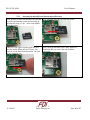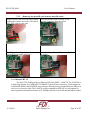
1
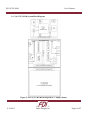
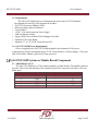
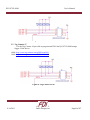
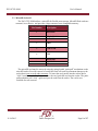
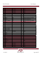
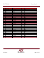
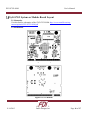
User’s Manual SYG-S7G2-SOM Copyright ©2015, Future Designs, Inc., All Rights Reserved ΣYG-S7G2-SOM User’s Manual Important Legal Information Information in this document is provided solely to enable the use of Future Designs, Inc. (FDI) products. FDI assumes no liability whatsoever, including infringement of any patent or copyright. FDI reserves the right to make changes to these specifications at any time, without notice. No part of this document may be reproduced or transmitted in any form or by any means, electronic or mechanical, for any purpose, without the express written permission of Future Designs, Inc. 996 A Cleaner Way, Huntsville, AL 35805. NOTE: The inclusion of vendor software products in this kit does not imply an endorsement of the product by Future Designs, Inc. yG™ is a trademark of Future Designs, Inc. Renesas Synergy™ is a trademark of Renesas Electronics Corporation. Microsoft, MS-DOS, Windows, Windows XP, Microsoft Word are registered trademarks of Microsoft Corporation. Other brand names are trademarks or registered trademarks of their respective owners. Printed in the United States of America. For more information on FDI or our products please visit www.TeamFDI.com. 2015 Future Designs, Inc. All rights reserved. 11/18/2015 Copyright ©2015, Future Designs, Inc Page 2 of 17 ΣYG-S7G2-SOM User’s Manual Table of Contents Important Legal Information ......................................................................................................................................... 2 ΣyG-S7G2 System on Module (SOM) Overview ............................................................................................. 4 1.1 Introduction ................................................................................................................................................... 4 1.2 ESD Warning ................................................................................................................................................ 4 1.3 Renesas Synergy S7G2 Microcontoller Block Diagram ............................................................................... 5 1.4 ΣyG-S7G2 SOM System Block Diagram ..................................................................................................... 6 1.5 Requirements ................................................................................................................................................. 7 1.6 ΣyG-S7G2 SOM Power Requirements ......................................................................................................... 7 ΣyG-S7G2 SOM System on Module Board Components ................................................................................ 7 2.1 ARM Mini-JTAG J2 ..................................................................................................................................... 7 2.2 Tag Connect J7 .............................................................................................................................................. 8 2.3 MicroSD Socket J1........................................................................................................................................ 9 2.3.1 Inserting the microSD card into the microSD socket .......................................................................... 10 2.3.2 Removing the microSD card from the microSD socket ...................................................................... 11 2.4 Ethernet PHY U5 ........................................................................................................................................ 11 2.5 200-pin SOMDIMM Connector Details J4 ................................................................................................. 12 ΣyG-S7G2 System on Module Board Layout ................................................................................................. 16 3.1 Schematics ......................................................................................................................................................... 16 3.2 Mechanicals ....................................................................................................................................................... 16 Support ............................................................................................................................................................ 17 4.1 Where to Get Help ....................................................................................................................................... 17 4.2 Useful Links ................................................................................................................................................ 17 11/18/2015 Copyright ©2015, Future Designs, Inc Page 3 of 17 ΣYG-S7G2-SOM User’s Manual ΣyG-S7G2 System on Module (SOM) Overview 1.1 Introduction The ΣyG-S7G2 System on Module (SOM) provides a quick and easy solution for implementing Renesas SynergyTM into a design, by providing the basic functions necessary for a product on an easy to use SODIMM. The ΣyG-S7G2 SOM uses an industry standard 200pin SODIMM interface and is compatible with FDI’s ΣyGTM Modular Development LCD Kits. It can also be used for custom platform development or customer applications. 1.2 ESD Warning The ΣyG-S7G2 SOM is shipped in a protective anti-static package. Do not subject the module to high electrostatic potentials. Exposure to high electrostatic potentials may cause damage to the boards that will not be covered under warranty. General practice for working with static sensitive devices should be followed when working with the kit. 11/18/2015 Copyright ©2015, Future Designs, Inc Page 4 of 17 ΣYG-S7G2-SOM User’s Manual 1.3 Renesas Synergy S7G2 Microcontoller Block Diagram Figure 1: S7G2 System Block Diagram 11/18/2015 Copyright ©2015, Future Designs, Inc Page 5 of 17 ΣYG-S7G2-SOM User’s Manual 1.4 ΣyG-S7G2 SOM System Block Diagram Figure 2: ΣYG-S7G2 Kit Block Diagram (4.3” display shown) 11/18/2015 Copyright ©2015, Future Designs, Inc Page 6 of 17 ΣYG-S7G2-SOM User’s Manual 1.5 Requirements The ΣyG-S7G2 SOM requires a development kit such as the ΣyG-S7G2 Modular Development Kit. Each yG development kit includes: • ΣyG-S7G2 System on Module (SOM) • Renesas Synergy Software Platform • Carrier Board • 5 VDC, 2.3A North American Power Supply • USB and Ethernet Cables • Segger ARM Cortex-M Mini-JTAG debugger and cables • Optional LCD Carrier Board • Optional 4.3” or 7.0″ PCAP Touch Screen LCD 1.6 ΣyG-S7G2 SOM Power Requirements Power is supplied to the yG-S7G2 SOM through the development kit. The power requirement for all yG development kits is 5V DC Center Positive 2A Power Supply. The power load of the SOM is 300mA typical and 475mA max load. ΣyG-S7G2 SOM System on Module Board Components 2.1 ARM Mini-JTAG J2 The ΣyG-S7G2 SOM uses a JTAG connector based on a 2mm header. This smaller connector provides 100% of the functionality of the standard 20-pin JTAG connector, but utilizes 70% less board space. Pin Number Description Pin Number Description 1 2 3 4 5 VCC TMS GND TCK GND 6 7 8 9 10 TDO X TDI GND JST# 11/18/2015 Copyright ©2015, Future Designs, Inc Page 7 of 17 ΣYG-S7G2-SOM User’s Manual Figure 3: ARM Mini JTAG 2.2 Tag Connect J7 Use the Tag Connect 10-pin cable to program and JTAG the ΣyG-S7G2 SOM using a Segger J-Link device. Cable: http://www.tag-connect.com/tc2050-arm2010 Cable: http://www.tag-connect.com/TC2050-IDC-NL Figure 4: Tag-Connect JTAG 11/18/2015 Copyright ©2015, Future Designs, Inc Page 8 of 17 ΣYG-S7G2-SOM User’s Manual 2.3 MicroSD Socket J1 The ΣyG-S7G2 SOM utilizes a microSD for flexible mass storage. MicroSD flash cards are common, cost effective, and provides a large amount of user-changeable memory. Pin Number Description 1 DAT2/RSV 2 CD_DAT3/CS# 3 CMD/SDI 4 VDD 5 CLK/SCLK 6 VSS 7 DAT0/SDO 8 DAT1/RSV CD 9 The microSD card must be removed using the spring loaded “push-pull” mechanism on the microSD socket. Forceful removal of a microSD card will result in permanent damage to the socket that is not covered under warranty. To insert the card, push it into the socket until a “click” sound is heard. Similarly, to remove the card, push the card into the socket. The pushpull mechanism will “click” again and eject the card from the socket. The card is now available for safe removal. 11/18/2015 Copyright ©2015, Future Designs, Inc Page 9 of 17 ΣYG-S7G2-SOM User’s Manual 2.3.1 : Inserting the microSD card into the microSD socket First, prepare to insert the microSD card into the Next, partially insert the card into the socket. socket by positioning it with its text facing up. Position the ridge, or “lip”, of the card furthest from the socket. Then, use your figure to gently push the card into the socket. When the card “clicks” into place it is in its final, locked position. The card is now ready for use. Note: Once the microSD card is fully inserted it should not fall out, even if the unit is shaken vigorously. 11/18/2015 Copyright ©2015, Future Designs, Inc Page 10 of 17 ΣYG-S7G2-SOM User’s Manual 2.3.2 : Removing the microSD card from the microSD socket Begin to remove the microSD card by gently Once the microSD card is ejected, it will pushing the card into the socket. The socket partially extend out from the socket. will “click” and eject the card. Carefully grab the ridged edge or sides of the microSD card to gently pull it out. The microSD card is now fully removed from the socket. 2.4 Ethernet PHY U5 The ΣyG-S7G2 SOM provides an Ethernet PHY from SMSC, LAN8720. The LAN8720 is a single chip solution for a 100BASE-TX/10BASE-T physical layer transceiver. It has support for reduced MII (RMII), and HP MDI-X auto crossover allowing for any standard Ethernet cable to be used, even a crossover cable. The LAN8720 is fully compliant to IEEE 802.3u with support for auto-negotiation and manual selection of 10/100Mbps speed as well as full and half-duplex modes. 11/18/2015 Copyright ©2015, Future Designs, Inc Page 11 of 17 ΣYG-S7G2-SOM User’s Manual 2.5 200-pin SOMDIMM Connector Details J4 Pin 1 2 3 4 5 6 7 8 9 10 11 12 13 14 15 16 17 18 19 20 21 22 23 SOMDIMM Signal Name ETH_TXP ETH_RXP ETH_TXN ETH_RXN 3V3A GND ETH_LED0 ETH_LED1 VBAT_IN NC RSTIN# RST# GPIO13_USB_ID NC NC NC NC NC NC NC AVCC AVCC AVSS Application Details Ethernet Transmit Positive Ethernet Receive Positive Ethernet Transmit Negative Ethernet Receive Negative 3.3V Analog Ground Ethernet LED0 Ethernet LED1 Vdd Battery Input Not Connected Reset Input I/O O I O I P P O O P U I O Not connected Not connected Not connected Not connected Not connected Not connected Not connected U U U U U U U 24 25 26 27 28 29 30 31 32 33 34 35 36 37 38 39 40 41 42 43 44 45 46 47 48 49 50 51 52 53 GND GPIO25_LCDPWR GPIO26_LCDLE GPIO27_LCDCLK GPIO28_LCDFP GPIO29_LCDEN GPIO30_LCDLP GPIO31_LCDVDR4 GPIO32_LCDVDR5 GPIO33_LCDVDR6 GPIO34_LCDVDR7 GPIO35_SSLB2 GPIO36 3.3V GND 3.3V GND USBH_DP USBD_DP USBH_DM USBD_DM GPIO45_LCD_B2 GPIO46_LCD_B3 GPIO47_RD GPIO48_TD GPIO49 NC GPIO51_SPCK GPIO52 GPIO53_MISO Ground LCD Power Enable LCD Latch Enable LCD Clock LCD Data Bit 4 LCD Data Bit 5 LCD Data Bit 6 LCD Data Bit 7 GPIO GPIO 3.3V Power Ground 3.3V Power Ground USB Host Data Positive USB Device Data Postive USB Host Data Negative USB Device Data Negative P O O O O O O O O O O U U P P P P B B B B GPIO / CAN Receive Data GPIO / CAN Transmit Data GPIO Not connected I O B U SOMDIMM Connection Details Output from KSZ8041 Ethernet PHY Output from KSZ8041 Ethernet PHY Input to KSZ8041 Ethernet PHY Input to KSZ8041 Ethernet PHY Analog 3.3V Output from PHY Circuit Ethernet LED0 output from KSZ8041 Ethernet LED1 output from KSZ8041 Vdd for battery backup of internal RTC Reset input to POR IC TPS3801 Reset output from POR circuit Connected to S7G2 Port 2 bit 0 Connected to S7G2 Port 2 bit 1 Connected to S7G2 Port 2 bit 2 Connected to S7G2 Port 2 bit 3 Connected to S7G2 Port 2 bit 4 Connected to S7G2 Port 2 bit 5 Connected to S7G2 Port 2 bit 6 Connected to S7G2 Port 2 bit 7 Connected to S7G2 Port 2 bit 8 Connected to S7G2 Port 2 bit 9 Connected to S7G2 Port 2 bit 10 Connected to S7G2 Port 2 bit 11 Connected to S7G2 USB Port A D+ Connected to S7G2 USB Port B D+ Connected to S7G2 USB Port A DConnected to S7G2 USB Port B D- Connected to S7G2 Port 0 bit 0 Connected to S7G2 Port 0 bit 1 Connected to S7G2 Port 0 bit 2 11/18/2015 Copyright ©2015, Future Designs, Inc Page 12 of 17 ΣYG-S7G2-SOM User’s Manual Pin 54 55 56 57 SOMDIMM Signal Name GPIO51_SPCK GPIO55 GPIO56_MOSI GPIO57_TXD 58 GPIO58_RXD 59 60 61 62 63 NC GPIO60_USBD_UPLED GPIO61_USBD_CON GPIO62_RSCK GPIO63 64 65 66 67 68 69 70 71 72 73 74 75 76 77 78 79 80 81 82 83 84 85 86 87 88 89 90 91 92 93 94 95 96 97 98 99 100 101 102 103 104 105 GPIO64_MISO GPIO65_MOSI GPIO66 GPIO67 GPIO68_USBH_OVC GPIO69_TPIRQ GPIO70_AD0.0 GPIO71_AD0.1 GPIO72_AD0.2 GPIO73_AD0.5_DA1 GPIO74_SDA GPIO75_SCL GND GND GPIO78_ACC_IRQ NC GPIO80_RTC_IRQ NC NC NC NC NC GPIO86_LED_BR GPIO87_USBH_PPWR GPIO88_LCD_G2 GPIO89_LCD_G3 GPIO90_LCD_G4 GPIO91_LCD_G5 GPIO92_LCD_G6 GPIO93_LCD_G7 GPIO94_LCD_B4 GPIO95_LCD_B5 GPIO96_LCD_B6 GPIO97_LCD_B& GPIO98_USBD_VBUS GPIO99_AD0 NC GND GND NC NC NC Application Details I/O SOMDIMM Connection Details GPIO / Serial Transmit Data – For RS232 GPIO / Serial Receive Data – For RS232 Not connected GPIO / USB Device Up LED GPIO / USB Device Connect GPIO / SPI Clock GPIO O Connected to S7G2 Port 0 bit 10 I Connected to S7G2 Port 0 bit 11 U O O O O DO NOT USE! Connected to S7G2 Port 0 bit 13 Connected to S7G2 Port 0 bit 14 Connected to S7G2 Port 0 bit 15 Connected to S7G2 Port 0 bit 16 (used for EEPROM CS) Connected to S7G2 Port 0 bit 17 Connected to S7G2 Port 0 bit 18 GPIO / SPI MISO GPIO / SPI MOSI I O GPIO / USB Host Over Current GPIO / Touch IC IRQ Input GPIO / AD0 Bit 0 GPIO / AD0 Bit 1 GPIO / AD0 Bit 2 GPIO / AD0 Bit 3 GPIO / User IO I2C Bus SDA GPIO / User IO I2C Bus SCL Ground Ground GPIO / Accelerometer IRQ I I I I I I B O P P I Connected to S7G2 Port 0 bit 21 Connected to S7G2 Port 0 bit 22 Connected to S7G2 Port 0 bit 23 Connected to S7G2 Port 0 bit 24 Connected to S7G2 Port 0 bit 25 Connected to S7G2 Port 0 bit 26 Connected to S7G2 Port 0 bit 27 Connected to S7G2 Port 0 bit 28 GPIO / RTC IRQ Input Not connected Not connected Not connected Not connected Not connected I U U U U U Connected to S7G2 Port 1 bit 5 GPIO / USB Host Power Ctl LCD Data Bit 10 LCD Data Bit 11 LCD Data Bit 12 LCD Data Bit 13 LCD Data Bit 14 LCD Data Bit 15 LCD Data Bit 16 LCD Data Bit 17 LCD Data Bit 22 LCD Data Bit 23 USB Device VBus Sense Input O O O O O O O O O O O I Connected to S7G2 Port 1 bit 19 Connected to S7G2 Port 1 bit 20 Connected to S7G2 Port 1 bit 21 Connected to S7G2 Port 1 bit 22 Connected to S7G2 Port 1 bit 23 Connected to S7G2 Port 1 bit 24 Connected to S7G2 Port 1 bit 25 Connected to S7G2 Port 1 bit 26 Connected to S7G2 Port 1 bit 27 Connected to S7G2 Port 1 bit 28 Connected to S7G2 Port 1 bit 29 Connected to S7G2 Port 1 bit 30 Not connected Ground Ground Not connected Not connected Not connected B P P U U U Unused Connected to S7G2 Port 1 bit 2 Unused Unused Unused 11/18/2015 Copyright ©2015, Future Designs, Inc Page 13 of 17 ΣYG-S7G2-SOM User’s Manual Pin 106 107 108 109 110 111 112 113 114 115 116 117 118 119 120 121 122 123 SOMDIMM Signal Name NC NC NC NC NC NC NC 5V0 5V0 NC GPIO116 GPIO117 GPIO118 GPIO119 GPIO120 GPIO121 GPIO122 GPIO123_SPKR_DA0 Application Details Not connected Not connected Not connected Not connected Not connected Not connected Not connected 5.0V Power 5.0V Power Not connected GPIO GPIO GPIO GPIO GPIO GPIO GPIO GPIO I/O U U U U U U U P P U B B B B B B B O SOMDIMM Connection Details 124 125 126 127 128 129 130 131 132 133 134 135 136 137 138 139 140 141 142 143 144 145 146 147 148 149 150 151 152 153 154 155 156 157 158 159 GPIO124 GPIO125 GPIO126 GPIO127_LCD_R2 GPIO128_LCD_R3 GND GND GPIO131_LCD18B GPIO132_LCD19B GPIO133_LCD20B GPIO134_LCD21B GPIO135_LCD22B GPIO136_LCD23B NC GPIO138 GPIO139 NC GPIO141 GPIO142 GPIO143 GPIO144 GPIO145 GPIO146 GPIO147 GPIO148 GPIO149_RX GPIO150_TX GPIO151 GPIO152 GPIO153 NC NC NC NC NC NC GPIO B Ground Ground P P Not connected U Unused Not connected U Unused Unused Unused Unused Unused Unused Unused Unused Unused Connected to S7G2 Port 2 bit 14 / VOL_UD Connected to S7G2 Port 2 bit 15 / AMP_MODE Connected to S7G2 Port 2 bit 19 / RS485 Ren Connected to S7G2 Port 2 bit 21 / RS485 DE Connected to S7G2 Port 2 bit 22 Connected to S7G2 Port 2 bit 23 Connected to S7G2 Port 2 bit 25 Connected to S7G2 Port 2 bit 26 / SPEAKER OUTPUT Connected to S7G2 Port 2 bit 27 RS485 RS485 Not connected Not connected Not connected Not connected Not connected Not connected U U U U U U Unused Unused Unused Unused Unused Unused 11/18/2015 Copyright ©2015, Future Designs, Inc Page 14 of 17 ΣYG-S7G2-SOM User’s Manual Pin 160 161 162 163 164 165 166 167 168 169 170 171 172 173 174 175 176 177 178 179 180 181 182 183 184 185 186 187 188 189 190 191 192 193 194 195 196 197 198 199 200 SOMDIMM Signal Name GPIO160_MD NC GPIO162_NMI GND GND 3.3V GND NC NC NC NC NC NC NC NC NC NC NC NC NC NC NC NC NC NC NC NC NC NC NC NC NC NC NC TMS TCK TDO TDI NC 3.3V GND Application Details I/O Not connected Not connected Ground Ground 3.3V Power Ground Not connected Not connected Not connected Not connected Not connected Not connected Not connected Not connected Not connected Not connected Not connected Not connected Not connected Not connected Not connected Not connected Not connected Not connected Not connected Not connected Not connected Not connected Not connected Not connected Not connected Not connected Not connected U U P P P P U U U U U U U U U U U U U U U U U U U U U U U U U U U Not connected 3.3V Power Ground U P P SOMDIMM Connection Details Unused Unused Unused Unused Unused Unused Unused Unused Unused Unused Unused Unused Unused Unused Unused Unused Unused Unused Unused Unused Unused Unused Unused Unused Unused Unused Unused Unused Unused Unused 11/18/2015 Copyright ©2015, Future Designs, Inc Page 15 of 17 ΣYG-S7G2-SOM User’s Manual ΣyG-S7G2 System on Module Board Layout 3.1 Schematics Visit this link for schematics of the SYG-S7G2-SOM: http://www.teamfdi.com/wpcontent/uploads/SYG-S7G2-SOM.pdf 3.2 Mechanicals Figure 5: S7G2 Top Figure 6: S7G2 Bottom 11/18/2015 Copyright ©2015, Future Designs, Inc Page 16 of 17 ΣYG-S7G2-SOM User’s Manual Support 4.1 Where to Get Help Online technical support is available at http://www.teamfdi.com/support/. 4.2 Useful Links Future Designs, Inc. Forums: http://www.teamfdi.com/?post_type=forum SYG-S7G2-SOM Product Page: http://www.teamfdi.com/product-details/syg-s7g2-som/ Renesas Synergy: https://synergybeta.renesas.com/ SEGGER J-Link LITE: https://www.segger.com/jlink-lite-cortexm.html Renesas Forums: http://www.renesasrulz.com/ 11/18/2015 Copyright ©2015, Future Designs, Inc Page 17 of 17