1
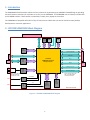
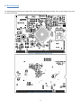
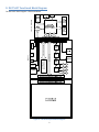
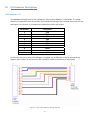
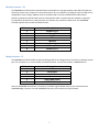
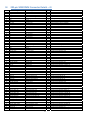
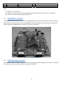
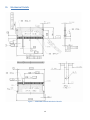
SOMDIMM‐LPC3250 Users Manual For use with Touch Screen LCD Kit Copyright ©2009, Future Designs, Inc., All Rights Reserved Table of Contents 1. Introduction ___________________________________________________________________________________ 1 2. LPC3250 SOMDIMM Block Diagram ________________________________________________________________ 1 3. Functional Description __________________________________________________________________________ 2 4. ESD Warning __________________________________________________________________________________ 2 5. Requirements _________________________________________________________________________________ 2 6. SOMDIMM‐LPC3250 Power Requirements __________________________________________________________ 2 7. Setting up the Hardware _________________________________________________________________________ 3 8. Board Layout __________________________________________________________________________________ 4 9. DK‐TS‐KIT Functional Block Diagram ________________________________________________________________ 5 10. I/O Connector Descriptions _______________________________________________________________________ 6 JTAG Connector – P6 ______________________________________________________________________________ 6 MicroSD Connector – P1 ___________________________________________________________________________ 7 Debug Connector – J5 _____________________________________________________________________________ 7 11. On Board Functions _____________________________________________________________________________ 8 Ethernet PHY – U8 ________________________________________________________________________________ 8 MicroSD – J2 ____________________________________________________________________________________ 8 Reset Generator – U3 _____________________________________________________________________________ 8 Serial EEPROM – U2 _______________________________________________________________________________ 8 12. 200‐pin SOMDIMM Connector Details – J4 __________________________________________________________ 9 13. SOMDIMM Installation _________________________________________________________________________ 12 14. SOMDIMM Socket Details _______________________________________________________________________ 12 15. Mechanical Details ____________________________________________________________________________ 13 16. Software ____________________________________________________________________________________ 14 17. Schematics ___________________________________________________________________________________ 15 18. Table of Figures _______________________________________________________________________________ 15 Information in this document is provided solely to enable the use of Future Designs products. FDI assumes no liability whatsoever, including infringement of any patent or copyright. FDI reserves the right to make changes to these specifications at any time, without notice. No part of this document may be reproduced or transmitted in any form or by any means, electronic or mechanical, for any purpose, without the express written permission of Future Designs, Inc. 2702 Triana Blvd, Huntsville, AL 35805 NOTE: The inclusion of vendor software products in this kit does not imply an endorsement of the product by Future Designs, Inc. 2009 Future Designs, Inc. All rights reserved. Microsoft, MS‐DOS, Windows, Windows XP, Microsoft Word are registered trademarks of Microsoft Corporation. Other brand names are trademarks or registered trademarks of their respective owners. FDI PN: MA00014 Revision: 3.2, 3/9/2011 6:22:00 PM Printed in the United States of America ii 1. Introduction The SOMDIMM‐LPC3250 provides a quick and easy solution for implementing an ARM926EJ‐S based design by providing the basic functions necessary for a product on an easy to use SOMDIMM . The SOMDIMM uses an industry standard 200 pin SO‐DIMM interface. These sockets are utilized by virtually every laptop on the market. This SOMDIMM is compatible with FDI’s Family of Touch Screen LCD Kits but can also be used for custom platform development or customer applications. 2. LPC3250 SOMDIMM Block Diagram CARRIER USER I/O TEMP, ACCEL, RTC, PBTNS, LEDS, EXTERNAL MINI JTAG JTAG UART5 I2C_1 uSD Socket SERVICE_N DEBUG SERIAL UART5 1KX8 SECURE EEPROM I2C_2 DIMM MODULE BORDER SPK SD INTERFACE 16-BIT TFT I2S_1 KSZ8041 ETH PHY 10/100 ETHERNET LPC3250 ARM926EJ-S based Microprocessor RMII LCD Interface I2S EXPANSION TOUCH INTERFACE SPI_1 UART1 RS232 SERIAL UART2, 3, 4, 6, & 7 ISP1301 USB OTG PHY USB HOST USB ATX MISC EXP GPIO (16) 3.3V 5.0V 0.9V-1.35V VCORE PS 1.8V & 1.2V PS 16-BIT DATA 22 CTRL NOTE: ONLY ONE USB INTERFACE MAY BE UTILIZED AT A TIME HIGHCORE 0.9V-1.2V 1.2V 1.8V 32MX16 DDR SDRAM VFBGA60 (64MX16 OPT) 14 DATA & CTRL USB DEVICE 4G NAND FLASH TSOP48 DIMM MODULE BORDER Figure 1 – LPC3250 SOMDIMM Block Diagram 1 NOTE: UART4 & UART7 ARE ONLY AVAILABLE WHEN LCD IS NOT UTILIZED 3. Functional Description SOMDIMM‐LPC3250 LPC3250 ARM926EJ‐S based microprocessor 64MB* DDR SDRAM (64 mega‐bytes) 512MB* NAND FLASH (512 mega‐bytes) 1KB I2C‐Serial EEPROM with Access Protection 10/100 Ethernet PHY Micro SD Card Socket (both SD and SDHC modes supported) JTAG Debug serial connector (OPTIONAL) Power‐on Reset Generator * Rev 2 board and later 4. ESD Warning The DK‐TS‐KIT shipped in a protective anti‐static package. The kit must not be subjected to high electrostatic potentials. Damage may occur to the boards that will not be covered under warranty. General practice for working with static sensitive devices should be followed when working with the DK‐TS‐KIT. 5. Requirements The SOMDIMM‐LPC3250 requires a carrier board with a 200‐pin SO‐DIMM socket. The socket should have the key at the 1.8V location (This has nothing to do with operation of the SOMDIMM‐LPC3250, it is simply a ‘key’ in the socket) The SOMDIMM‐LPC3250 requires only 3.3V & 5.0V for operation. The CARRIER Board from Future Designs provides this socket and should be utilized to develop your application for initial verification. Example SO‐DIMM Socket Manufacturer and Part Number: TYCO 1473005‐4 Please refer to section 10 for the pin out details of the SOMDIMM Edge Finger. 6. SOMDIMM‐LPC3250 Power Requirements The SOMDIMM‐LPC3250 typical power consumption was measured at room temperature, 266MHz core clock rate. Voltage Power On, booting Linux booted, login prompt Observed Max 3.3V 148mA 185mA 333mA 5V 17mA 2mA 25mA 2 7. Setting up the Hardware The following are step by step instructions for setting up the hardware. 1) Make sure you have an SOMDIMM‐LPC3250 board plugged into the CARRIER board at J1. 2) Verify the LCD Interface ribbon cable connects the CARRIER board to the LCD CARRIER (J7) board. 3) With the power off, plug the 5V center‐positive Power Supply into 5V (P5) of the CARRIER board. 4) Connect an RJ‐45 Ethernet cable to the ETHERNET (J5) interface of the CARRIER board. 5) Plug in a female‐to‐female DB9 serial cable (included in the DK‐TS‐KIT) between PC and RS232 (P4) 6) Open a serial program on the PC (such as HyperTerminal or PUTTY) and set the serial connection to 115200 baud, 8 bits, 1 stop bit, no parity. 7) Insert a flash media drive with the demonstration files (included) into USB HOST (P1). 8) Turn on the power. The boot screen will appear showing the board information and FDI logo. After a short time, Tux the Penguin will appear in the upper left as Linux continues to boot. 9) If you have a current version of the software, the program will then automatically show a slideshow loaded from the previously inserted flash drive. 10) If not, the slideshow can be started by doing the following steps: a. When the login screen appears, enter “root” as the login and “root” as the password. b. At the command prompt type the command, “./usbslides” c. The slideshow should start after a few seconds. 3 8. Board Layout The following figures illustrate the layout of the various components of the DK‐TS‐KIT. They are for reference only and are subject to change. Figure 2 – SOMDIMM‐LPC3250 Top Side Figure 3 – SOMDIMM‐LPC3250 Bottom Side 4 9. DK‐TS‐KIT Functional Block Diagram The DK‐TS‐KIT Block Diagram is illustrated below. I/O LCD LCD SIGNALS EXPANSION CONNECTORS EXPANSION SIGNALS I2S EXPANSION EXP SOMDIMM-LPC3250 CARRIER Figure 4 – DK‐TS‐KIT System Block Diagram 5 10. I/O Connector Descriptions JTAG Connector – P6 The SOMDIMM‐LPC3250 utilizes a new, reduced size JTAG connector based on a 2mm Header. This smaller connector provides 100% of the functionality of the standard 20‐pin large JTAG connector, but utilizes 70% less board space. The connector is a standard part available from most major vendors. Pin Number Description 1 2 3 4 5 6 7 8 9 10 3.3V TRSTn TDI TMS TCK RTCK TDO Reset Ground 5.0V For users that may have existing JTAG debuggers, an adapter may be fabricated using the following wiring diagram: (part numbers for the connectors are included from both the manufacturer and Digi‐key) Figure 5 – Mini JTAG Adapter Wiring Diagram 6 MicroSD Connector – P1 The SOMDIMM‐LPC3250 utilizes a MicroSD Socket for flexible mass storage capability. MicroSD Flash Cards are utilized by almost every cell phone on the market and are very cost effective, providing as much as 16GB of user‐ changeable memory storage. Adapter cards are available (and are usually included with the MicroSD) to facilitate installation of the MicroSD card into a standard SD reader. microSD cards are available in capacities from 64 MB to 16 GB but most cards with sizes over 2GB are only available as SDHC cards. The SOMDIMM‐ LPC3250 supports both microSD and SDHC formats. Pin Number 1 2 3 4 5 6 7 8 Description MS Data I/O 2 MS Data I/O 3 MS BS 3.3V MS SCLK Ground MS Data I/O 0 MS Data I/O 1 Debug Connector – J5 The SOMDIMM‐LPC3250 includes an optional debug header that is designed to be utilized as an optional console port. This connector is a 1.5mm JST Male, shrouded connector. The JST Part Number is: SM06B‐SHLS‐TF. Pin Number 1 2 3 4 5 6 Description 3.3V Reset Input NC Ground UART5 RXD (Input) UART5 TXD (Output) Note: On SOMDIMM‐LPC3250 Rev 2.0 and later, the UART5 signals (RXD & TXD) are also connected to the SOMDIMM edge connector. See the SOMDIMM Connector pinout section for specific details. 7 11. On Board Functions Ethernet PHY – U8 The SOMDIMM‐LPC3250 provides an Ethernet PHY from Micrel, KSZ8041NL. The KSZ8041NL is a single chip solution for a 100BASE‐TX/10BASE‐T physical layer transceiver. It has support for media independent interface (MII), reduced MII (RMII), and HP MDI/MDI‐X auto crossover. This allows for any standard Ethernet cable to be used, even a crossover cable. The KSZ8041NL is fully compliant to IEEE 802.3u with support for auto‐negotiation and manual selection of 10/100Mbps speed as well as full and half‐duplex modes. For detailed information, please refer to the specific data sheet for this device available from the manufacturer. MicroSD – J2 The SOMDIMM‐LPC3250 provides a MicroSD interface for access to a removable Flash memory. Micro Secure Digital cards are one of the lowest prices per capacity memory cards available. They allow the LPC3250 to have access to a much larger amount of Flash memory in a very small form factor. When using a MicroSD card it can be accessed via the SD controller of the LPC3250. Reset Generator – U3 The SOMDIMM‐LPC3250 utilizes a TPS3801 power‐on reset supervisor and voltage monitor. The TPS3801 includes an external reset input that is connected to the reset button on the CARRIER Board. For detailed information, please refer to the specific data sheet for this device available from the manufacturer. Serial EEPROM – U2 The SOMDIMM‐LPC3250 includes a serial EEPROM, NXP PCA24S08. This device provides 1K‐Byte of serial electrically erasable and programmable Read‐only memory (EEPROM). Data is received and transmitted via the serial I2C bus. Access permissions limiting reads or writes can be set via the I2C‐bus to isolate blocks of memory from improper access. PCA24S08 Device I2C Bus 2 Address = 0xA8 For detailed information, please refer to the specific data sheet for this device available from the manufacturer. 8 12. 200‐pin SOMDIMM Connector Details – J4 Pin 1 2 3 4 5 6 7 8 9 10 11 12 13 14 15 16 17 18 19 20 21 22 23 24 25 26 27 28 29 30 31 32 33 34 35 36 37 38 39 40 41 42 43 44 45 46 47 48 49 50 51 52 53 54 55 56 57 58 59 60 61 62 63 SOMDIMM Signal Name ETH_TXP ETH_RXP ETH_TXN ETH_RXN 3V3A GND ETH_LED0 ETH_LED1 VBAT_IN ALARM RESET_IN RESET_OUT NC NC NC NC NC NC NC NC VDDA VREF VSSA GND GPIO25_LCDPWR GPIO26_LCDLE GPIO27_LCDCLK GPIO28_LCDFP GPIO29_LCDENAB GPIO30_LCDLP GPIO31_LCDVD4 GPIO32_LCDVD5 GPIO33_LCDVD6 GPIO34_LCDVD7 GPIO35 GPIO36 3.3V GND 3.3V GND USBH_DP USBD_DP USBH_DM USBD_DM GPIO45_LCDVD18 GPIO46_LCDVD19 GPIO47_RD GPIO48_TD GPIO49 GPIO50 GPIO51_I2SRX_CLK GPIO52_I2SRX_WS GPIO53_I2SRX_SDA GPIO54_I2STX_CLK GPIO55_I2STX_WS GPIO56_I2STX_SDA GPIO57_TXD GPIO58_RXD GPIO59_USBH_PWRD GPIO60_USBD_UPLED GPIO61_USBD_CON GPIO62_SCK GPIO63_TPCS Application Details Ethernet Transmit Positive Ethernet Receive Positive Ethernet Transmit Negative Ethernet Receive Negative 3.3V Analog Ground Ethernet LED0 Ethernet LED1 Vdd Battery Input Alarm Signal From Micro Reset Input Reset Output from POR Not connected Not connected Not connected Not connected Not connected Not connected Not connected Not connected Vdd Analog Reference Voltage Vss Analog Ground LCD Power Enable LCD Latch Enable LCD Clock LCD Data Bit 4 LCD Data Bit 5 LCD Data Bit 6 LCD Data Bit 7 GPIO Unused 3.3V Power Ground 3.3V Power Ground USB Host Data Positive USB Device Data Postive USB Host Data Negative USB Device Data Negative LCD Data Bit 18 LCD Data Bit 19 GPIO / CAN Receive Data GPIO / CAN Transmit Data GPIO GPIO GPIO / I2S Receive Clock GPIO / I2S Receive Write Sel GPIO / I2S Receive Data GPIO / I2S Transmit Clock GPIO / I2S Transmit Write Sel GPIO / I2S Transmit Data GPIO / Serial Transmit Data GPIO / Serial Receive Data GPIO / USB Host Power Detect GPIO / USB Device Up LED GPIO / USB Device Connect GPIO / SPI Clock GPIO / Touch IC Chip Sel I/O O I O I P P O O P O I O U U U U U U U U I I I P O O O O O O O O O O U U P P P P B B B B O O I O B B O O I O O B O I I O O O O 9 SOMDIMM Connection Details Output from KSZ8041 Ethernet PHY Output from KSZ8041 Ethernet PHY Input to KSZ8041 Ethernet PHY Input to KSZ8041 Ethernet PHY Analog 3.3V Output from PHY Circuit Ethernet LED0 output from KSZ8041 Ethernet LED1 output from KSZ8041 Vdd for battery backup of internal RTC Reset input to POR IC TPS3801 Reset output from POR circuit ADC Power Supply ADC Reference Voltage Input ADC Ground Connected to LPC3250 Pin E11 Connected to LPC3250 Pin B12 Connected to LPC3250 Pin B13 Connected to LPC3250 Pin A14 Connected to LPC3250 Pin D10 Connected to LPC3250 Pin D11 Connected to LPC3250 Pin M17 Connected to LPC3250 Pin M18 Connected to LPC3250 Pin L15 Connected to LPC3250 Pin L16 Connected to LPC3250 Pin C2 (GPO_19) Connected to LPC3250 Pin N18 (GPO_17) Connected to ISP1301 Pin 16 Connected to ISP1301 Pin 16 Connected to ISP1301 Pin 15 Connected to ISP1301 Pin 15 Connected to LPC3250 Pin A16 Connected to LPC3250 Pin D15 Connected to LPC3250 Pin A12 (GPIO_00) Connected to LPC3250 Pin B2 (GPO_20) Connected to LPC3250 Pin D3 (GPO_14) Connected to LPC3250 Pin E8 (GPIO11)) Connected to LPC3250 Pin B5 (P0_0) Connected to LPC3250 Pin D7 (P0_1) Connected to LPC3250 Pin C16 (GPI_00) Connected to LPC3250 Pin A4 (MAT3_0) Connected to LPC3250 Pin B4 (CAP3_0) Connected to LPC3250 Pin E7 (MAT3_1) Connected to LPC3250 Pin K16 Connected to LPC3250 Pin K15 (GPI_15) Connected to LPC3250 Pin B16 (GPI_08) Connected to LPC3250 Pin D4 (GPO_01) Connected to LPC3250 Pin D8 (GPO_04) Connected to LPC3250 Pin C9 Connected to LPC3250 Pin E9 (GPIO_05) 64 65 66 67 68 69 70 71 72 73 74 75 76 77 78 79 80 81 82 83 84 85 86 87 88 89 90 91 92 93 94 95 96 97 98 99 100 101 102 103 104 105 106 107 108 109 110 111 112 113 114 115 116 117 118 119 120 121 122 123 124 125 126 127 128 129 130 GPIO64_MISO GPIO65_MOSI GPIO66_ESDA GPIO67_ESCL GPIO68_USBH_OVC GPIO69_TPIRQ GPIO70_AD0.0 GPIO71_AD0.1 GPIO72_AD0.2 GPIO73_AD0.3 GPIO74_SDA GPIO75_SCL GND GND GPIO78_ACC_IRQ (1) GPIO79_SERVICEN GPIO80_RTC_IRQ NC NC NC NC NC GPIO86_LED_BR GPIO87_USBH_PPWR GPIO88_LCDVD10 GPIO89_LCDVD11 GPIO90_LCDVD12 GPIO91_LCDVD13 GPIO92_LCDVD14 GPIO93_LCDVD15 GPIO94_LCDVD20 GPIO95_LCDVD21 GPIO96_LCDVD22 GPIO97_LCDVD23 GPIO98_USBD_VBUS GPIO99_AD0.5 GPIO100 GND GND NC NC NC NC NC NC NC NC NC NC 5V0 5V0 NC GPIO116 GPIO117 GPIO118 GPIO119 GPIO120 GPIO121 GPIO122 GPIO123_SPKR GPIO124 NC NC GPIO127_LCDVD2 GPIO128_LCDVD3 GND GND GPIO / SPI MISO GPIO / SPI MOSI GPIO / External I2C SDA GPIO / External I2C SCL GPIO / USB Host Over Current GPIO / Touch IC IRQ Input GPIO / AD0 Bit 0 GPIO / AD0 Bit 1 GPIO / AD0 Bit 2 GPIO / AD0 Bit 3 GPIO / User IO I2C Bus SDA GPIO / User IO I2C Bus SCL Ground Ground GPIO / Accelerometer IRQ GPI_01 Bit / Service_N Select GPIO / RTC IRQ Input Not connected Not connected Not connected Not connected Not connected GPIO / LED Backlight Bright GPIO / USB Host Power Ctl LCD Data Bit 10 LCD Data Bit 11 LCD Data Bit 12 LCD Data Bit 13 LCD Data Bit 14 LCD Data Bit 15 LCD Data Bit 16 LCD Data Bit 17 LCD Data Bit 22 LCD Data Bit 23 USB Device VBus Sense Input Not connected GPIO Ground Ground Not connected Not connected Not connected Not connected Not connected Not connected Not connected Not connected Not connected Not connected 5.0V Power 5.0V Power Not connected GPIO GPIO GPIO GPIO GPIO GPIO GPIO GPIO GPIO Not connected Not connected LCD Data Bit 2 LCD Data Bit 3 Ground Ground I O B I I I I I I I B O P P I I I U U U U U O O O O O O O O O O O O I I B P P U U U U U U U U U U P P U B B B B B B B O B U U O O P P 10 Connected to LPC3250 Pin C10 Connected to LPC3250 Pin B9 Connected to LPC3250 Pin B6 (I2C1_SDA) Connected to LPC3250 Pin A5 (I2C1_SCL) Connected to LPC3250 Pin C7 (GPI_06) Connected to LPC3250 Pin E13 (GPI_04) Connected to LPC3250 Pin T14 Connected to LPC3250 Pin U15 Connected to LPC3250 Pin R13 Connected to LPC3250 Pin U16 Connected to LPC3250 Pin B6 (I2C1_SDA) Connected to LPC3250 Pin A5 (I2C1_SCL) Connected to LPC3250 Pin F4 (GPI_03) Connected to LPC3250 Pin C15 (GPI_01) Connected to LPC3250 Pin D13 (GPI_07) Connected to LPC3250 Pin D14 (PWM_OUT1) Connected to ISP1301 Pin 1 (ADR/PSW) Connected to LPC3250 Pin E17 Connected to LPC3250 Pin E18 Connected to LPC3250 Pin L17 Connected to LPC3250 Pin L18 Connected to LPC3250 Pin E10 Connected to LPC3250 Pin G17 Connected to LPC3250 Pin A9 Connected to LPC3250 Pin A10 Connected to LPC3250 Pin B11 Connected to LPC3250 Pin B10 Connected to LPC3250 Pin C14 (GPI_02) Connected to LPC3250 Pin J4 (P1_23) Connected to LPC3250 Pin J3 (P1_22) Connected to LPC3250 Pin J2 (P1_21) Connected to LPC3250 Pin J1 (P1_20) Connected to LPC3250 Pin K1 (P1_19) Connected to LPC3250 Pin K2 (P1_18) Connected to LPC3250 Pin K4 (P1_17) Connected to LPC3250 Pin K3 (P1_16) Connected to LPC3250 Pin B14 (GPO_02/MAT1_0) Connected to LPC3250 Pin L1 (P1_15) Connected to LPC3250 Pin A15 Connected to LPC3250 Pin A13 131 132 133 134 135 136 137 138 139 140 141 142 143 144 145 146 147 148 149 150 151 152 153 154 155 156 157 158 159 160 161 162 163 164 165 166 167 168 169 170 171 172 173 174 175 176 177 178 179 180 181 182 183 184 185 186 187 188 189 190 191 192 193 194 195 196 197 NC NC NC NC NC NC NC (1) GPIO138_U6_RX (1) GPIO139_U6_TX NC NC (1), (2) GPIO142_U4_RX NC NC (1) GPIO145_U3_RX (1) GPIO146_U3_TX NC NC (1) GPIO149_U2_RX (1) GPIO150_U2_TX (1) , (3) GPIO151_U5_RX (1) , (3) GPIO152_U5_TX NC NC NC NC NC NC NC NC NC NC GND GND 3.3V GND NC NC NC NC NC NC NC NC NC NC NC NC NC NC NC NC NC NC NC NC NC NC NC NC NC NC NC NC NC NC NC Not connected Not connected Not connected Not connected Not connected Not connected Not connected UART6 Receive Data UART6 Transmit Data Not connected Not connected UART4 Receive Data Not connected Not connected UART3 Receive Data UART3 Transmit Data Not connected Not connected UART2 Receive Data UART2 Transmit Data UART5 Receive Data UART5 Transmit Data Not connected Not connected Not connected Not connected Not connected Not connected Not connected Not connected Not connected Not connected Ground Ground 3.3V Power Ground Not connected Not connected Not connected Not connected Not connected Not connected Not connected Not connected Not connected Not connected Not connected Not connected Not connected Not connected Not connected Not connected Not connected Not connected Not connected Not connected Not connected Not connected Not connected Not connected Not connected Not connected Not connected Not connected Not connected Not connected Not connected U U U U U U U I O U U I U U I O U U I O I O U U U U U U U U U U P P P P U U U U U U U U U U U U U U U U U U U U U U U U U U U U U U U 11 Unused Unused Unused Unused Unused Unused Unused Connected to LPC3250 Pin F17 Connected to LPC3250 Pin G16 Unused Unused Connected to LPC3250 Pin B15 Unused Unused Connected to LPC3250 Pin J14 Connected to LPC3250 Pin J17 Unused Unused Connected to LPC3250 Pin K18 Connected to LPC3250 Pin K17 Connected to LPC3250 Pin F18 Connected to LPC3250 Pin H15 Unused Unused Unused Unused Unused Unused Unused Unused Unused Unused Unused Unused Unused Unused Unused Unused Unused Unused Unused Unused Unused Unused Unused Unused Unused Unused Unused Unused Unused Unused Unused Unused Unused Unused Unused Unused Unused Unused Unused Unused 198 199 200 NC 3.3V GND Not connected 3.3V Power Ground U P P Unused Notes: (1) Revision 2.0 s and later only (2) UART4 TX is located on multi‐use pin GPIO128_LCDVD3 and is only available when an LCD is not utilized. (3) UART5 is also connected to the Debug Connector, J1 13. SOMDIMM Installation The SOMDIMM‐LPC3250 should be inserted into the SOMDIMM Socket as shown below and then locked into place by pushing down to the Carrier Board. Ensure the SOMDIMM is inserted completely into the socket prior to locking. The socket utilized on the CARRIER Board is rated for a minimum of 25 insertions. Figure 6 – SOMDIMM Insertion 14. SOMDIMM Socket Details The SOMDIMM‐LPC3250 is designed to be used with a standard 200‐pin DDR2 SO‐DIMM Socket connector. An example connector part is as follows: Mfg: Tyco (AMP), Part Number: 1473005‐4. 12 15. Mechanical Details Figure 7 – SOMDIMM‐LPC3250 Mechanical Details 13 16. Software Below is a list of the software included with the SOMDIMM‐LPC3250 or DK‐TS‐KIT. Primary Bootloader (brings up system, configures memory and system clocks, loads U‐boot) o 266 MHz o SDRAM configuration o NAND configuration U‐Boot (Loads Linux, provides TFTP, upgrades Linux) o Serial EEPROM with configuration Linux Kernel o LPC3250 Processor (w/VFP support, enabled caches) o QVGA TFT LCD (320x240) w/frame buffer o Touch Screen o 10/100 Ethernet (TCP/IP) o Serial Port (both high speed port and optional debug UART) o MicroSD Support via SD Interface (Both SD & SDHC modes supported) o USB Host (Mass Storage, HID, etc.) o USB Device (via OTG and USB Linux Gadgets) o I2C Bus and Peripherals GPIO for buttons and LEDs RTC with SuperCap backup 3‐axis Digital Accelerometer Temperature Sensor o GPIO library o Speaker (piezo for beeps and tones) o JFFS2 (using unused MTD NAND memory, approx 16MB) o File Systems (FAT16, VFAT, EXT2) o WDT Release format o Patch files for Linux and U‐Boot o LTIB compatible release (via Bitshrine.org) Detailed software information may be included in a separate document or you can download the latest details from our website at www.teamfdi.com/DK‐TS‐KIT 14 17. Schematics Please see the website at: http://www.teamfdi.com/SOMDIMM‐LPC3250/index.html 18. Table of Figures Figure 1 – LPC3250 SOMDIMM Block Diagram ....................................................................................................................... 1 Figure 2 – SOMDIMM‐LPC3250 Top Side ................................................................................................................................ 4 Figure 3 – SOMDIMM‐LPC3250 Bottom Side.......................................................................................................................... 4 Figure 4 – DK‐TS‐KIT System Block Diagram ........................................................................................................................... 5 Figure 5 – Mini JTAG Adapter Wiring Diagram ....................................................................................................................... 6 Figure 6 – SOMDIMM Insertion ............................................................................................................................................ 12 Figure 7 – SOMDIMM‐LPC3250 Mechanical Details ............................................................................................................. 13 15