1
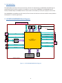
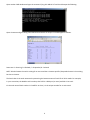
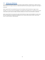
 SOMDIMM‐LPC2478 Users Manual For use with Touch Screen LCD Kit Copyright ©2009, Future Designs, Inc., All Rights Reserved
Table of Contents 1. Introduction ___________________________________________________________________________________ 4 2. LPC2478 SOMDIMM Block Diagram ________________________________________________________________ 4 3. Functional Description __________________________________________________________________________ 5 4. ESD Warning __________________________________________________________________________________ 5 5. Requirements _________________________________________________________________________________ 5 6. SOMDIMM‐LPC2478 Power Requirements __________________________________________________________ 5 7. Setting up the Hardware _________________________________________________________________________ 6 8. Demonstration Software Main Menu _______________________________________________________________ 7 9. PC to Demonstration Network Configuration _________________________________________________________ 8 10. Setting up a Slideshow _________________________________________________________________________ 10 11. Board Layout _________________________________________________________________________________ 11 12. DK‐TS‐KIT System Functional Block Diagram ________________________________________________________ 12 13. I/O Connector Descriptions ______________________________________________________________________ 13 JTAG Connector – J3 _____________________________________________________________________________ 13 MicroSD Connector – J2 __________________________________________________________________________ 14 ISP Connector – J5 _______________________________________________________________________________ 14 14. On Board Functions ____________________________________________________________________________ 15 Ethernet PHY – U8 _______________________________________________________________________________ 15 MicroSD – J2 ___________________________________________________________________________________ 15 Reset Generator – U3 ____________________________________________________________________________ 15 Serial EEPROM – U2 ______________________________________________________________________________ 15 15. 200‐pin SOMDIMM Connector Details – J4 _________________________________________________________ 16 16. SOMDIMM Installation _________________________________________________________________________ 19 17. SOMDIMM Socket Details _______________________________________________________________________ 19 18. Mechanical Details ____________________________________________________________________________ 20 19. Software ____________________________________________________________________________________ 21 20. Configuring Rowley CrossWorks CrossStudio for ARM® for J‐Link Flashing_________________________________ 23 21. Functional Test Software ________________________________________________________________________ 24 Configuring the Functional Test setup _____________________________________________________________ 24 Running Functional Test ________________________________________________________________________ 24 Installing the Demonstration Software via Flash Magic ________________________________________________ 25 22. Schematics ___________________________________________________________________________________ 26 23. Table of Figures _______________________________________________________________________________ 26 ii Information in this document is provided solely to enable the use of Future Designs products. FDI assumes no liability whatsoever, including infringement of any patent or copyright. FDI reserves the right to make changes to these specifications at any time, without notice. No part of this document may be reproduced or transmitted in any form or by any means, electronic or mechanical, for any purpose, without the express written permission of Future Designs, Inc. 2702 Triana Blvd, Huntsville, AL 35805. For more information on FDI or our products please visit www.teamfdi.com. NOTE: The inclusion of vendor software products in this kit does not imply an endorsement of the product by Future Designs, Inc. © 2009 Future Designs, Inc. All rights reserved. uEZ™ is a registered trademark of Future Designs, Inc. Microsoft, MS‐DOS, Windows, Windows XP, Microsoft Word are registered trademarks of Microsoft Corporation. Other brand names are trademarks or registered trademarks of their respective owners. FDI PN: MA00012 Revision: 3, 12/15/2009 4:38:00 PM Printed in the United States of America iii 1. Introduction The SOMDIMM‐LPC2478 provides a quick and easy solution for implementing an ARM7TDMI‐S based design by providing the basic functions necessary for a product on an easy to use SOMDIMM. The SOMDIMM uses an industry standard 200 pin SO‐DIMM interface. These sockets are utilized by virtually every laptop on the market. This SOMDIMM is compatible with FDI’s Family of Touch Screen LCD Kits but can also be used for custom platform development or customer applications. 2. LPC2478 SOMDIMM Block Diagram CARRIER USER I/O
TEMP, ACCEL, RTC, PBTNS, LEDS, EXTERNAL
DIMM MODULE BORDER
1KX8
SECURE
EEPROM
DEBUG
SERIAL
5.0V
MINI
JTAG
3.3V
3.3V
SPK
CAN
CONN
CAN1
TOUCH INTERFACE
16-BIT TFT
I2S
10/100
ETHERNET
KSZ8041
ETH
PHY
LPC2478
RMII
SPI_1
ARM7TDMI-S based
Microprocessor
UART2
USB
DEVICE
RS232
SERIAL
USBB DEVICE
MISC EXP GPIO
USB
HOST
USBA HOST
2MX32
SDRAM
TSOP
(4MX32 OPT)
uSD
Socket
DIMM MODULE BORDER
Figure 1 – LPC2478 SOMDIMM Block Diagram 4 3. Functional Description SOMDIMM‐LPC2478 • LPC2478 ARM7TDMI‐S based Microprocessor • 2Mx32 SDRAM (8Mega‐bytes) optional up to 32Mx32 • 1KB I2C‐Serial EEPROM with Access Protection • 10/100 Ethernet PHY • Micro SD Card Socket for up to 2Giga‐bytes storage (SDHC is not supported) • Mini JTAG • ISP Connector for use with USP‐ICP‐LPC2K • Power‐on Reset Generator 4. ESD Warning The DK‐TS‐KIT shipped in a protective anti‐static package. The kit must not be subjected to high electrostatic potentials. Damage may occur to the boards that will not be covered under warranty. General practice for working with static sensitive devices should be followed when working with the DK‐TS‐KIT. 5. Requirements The SOMDIMM‐LPC2478 requires a carrier board with a 200‐pin SO‐DIMM socket. The socket should have the key at the 1.8V location (the SOMDIMM‐LPC2478 doesn’t require 1.8V). The CARRIER Board from Future Designs provides this socket and should be utilized to develop your application for initial verification. Example SO‐DIMM Socket Manufacturer and Part Number: TYCO 1473005‐4 Please refer to section 10 for the pin out details of the SOMDIMM Edge Finger. 6. SOMDIMM‐LPC2478 Power Requirements The following power requirements were measured at room temperature at 72MHz operating clock rate: Voltage Booted at the uEZ Demo Screen Observed Max 3.3V 200mA 208mA 5 7. Setting up the Hardware The following are step by step instructions for setting up the hardware. 1) Make sure you have a SOMDIMM‐LPC2478 board plugged into the CARRIER board at J1. 2) Verify the LCD Interface ribbon cable connects the CARRIER board to the LCD CARRIER (J7) board. 3) With the power off, plug the 5V center‐positive Power Supply into 5V (P5) of the CARRIER board. 4) Connect an RJ‐45 Ethernet cable to the ETHERNET (J5) interface of the CARRIER board. 5) Plug in a female‐to‐female DB9 serial cable (included in the DK‐TS‐KIT) between PC and RS232 (P4) 6) Insert a flash media drive with the demonstration files (included) into USB HOST (P1). 7) If available, plug in a Mini‐USB cable to USB DEVICE (P6). 8) If available, plug in a CAN DB9 cable into CAN (P3). 9) Turn on the power. The title screen should appear and a short tune is played. The main menu will appear. 10) After connecting all of the above, your configuration should look as follows: 6 8. Demonstration Software Main Menu The Demonstration Software has the following options: • Slideshow Loads up to nine slides from the flash drive and allows the user to scroll up and down through the material. Slide back to the load screen to return to the main menu. See Setting up a Slideshow for details on how to customize. • Draw A very simple art program is provided. Use the touch screen to draw lines in the box to the right. Click on Color to rotate through a list of color choices. Save stores the graphic image as the file IMAGE.RAW on the USB Flash drive. Load recalls the saved graphic image from the USB Flash drive. • Console Presents an output screen showing what a remote user sees when Telnetting into the console. On a Windows PC, configure the PC as explained in PC to Demonstration Network Configuration, then open a CMD window and type “telnet 192.168.10.20” to connect to the DK‐TS‐KIT. Type “dir” to show the contents of the Flash drive that is plugged into the DK‐TS‐KIT. Type “quit” to disconnect. • Time & Temperature Displays the current time and date from the external Real Time Clock (RTC) and the temperature from the LM75 temperature sensor on the CARRIER board. • Accelerometer Demonstrates the accelerometer by moving a simulated ball across the screen as the CARRIER board is tilted along the X and Y axis. • Settings Displays the submenu screen. • Calibrate Calibrates the Touch Screen and stores the new calibration information in the EEPROM on the SOMDIMM. • Functional Test Provides a step by step test of all basic features of the DK‐TS‐KIT. Requires additional hardware to test all features. See Functional Test Software section for more details. • FCT Loopback Puts the unit into a mode that will communicate with another DK‐TS‐KIT running the Functional Test. See Functional Test Software section for more details. 7 9. PC to Demonstration Network Configuration In order to communicate via Ethernet to the DK‐TS‐KIT, the PC’s network configuration will need to be changed. The simplest method is to give the PC another IP number and add the PC to another subnet. If using Windows XP, follow these instructions. Other operating systems should have similar operations. Start by going to the Control Panel and select Network Connections. Then double click the Local Area Connection (or similarly named) and click Properties. The following dialog should appear. Scroll down to “Internet Protocol (TCP/IP)”, select, and then click Properties. On the next screen, the computer needs to be set to a static IP number. Enter the current IP address, subnet mask, default gateway, and DNS servers (enter the command “ipconfig /all” at a CMD window to get this information). Then click Advanced and then click Add… and enter the following information and then click Add. Click OK. Click OK. 8 Open another CMD window and type the command “ping 192.168.10.20” and should output the following: Open a browser and go to http://192.168.10.20 and watch the output. It should appear as follows: States are: R = Running, B = Blocked, S = Suspended, D = Deleted NOTE: Blocked means the task is waiting for an event and has a timeout specified, Suspended means it also waiting but has no timeout. The Stack value is the stack watermark representing the lowest amount of stack left in 32‐bit words. For example, in your screenshot, the WebSvr task has always had 150*4 = 600 bytes (or more) available in its stack. # is the task control block number in FreeRTOS. In short, it is the unique number for an active task. 9 10. Setting up a Slideshow The Slideshow demonstration loads and scrolls between images provided on a USB Flash drive. Images must be in 24 bit uncompressed Targa (.TGA) format. Adobe Photoshop and many other graphics programs can save images in this format. When using DK‐TS‐KIT’s with a QVGA LCD (e.g. DK‐57TS‐LPC2478 or DK‐35TS‐LPC2478), the images must be 320x240 in size and use the file names QSLIDE01.TGA, QSLIDE02.TGA, QSLIDE03.TGA, etc. QVGA LCD units can also use the older style file names: PICTURE1, PICTURE2, PICTURE3, etc. There is a limit of 38 slides in a slideshow. When using DK‐TS‐KIT’s with a VGA LCD (e.g. DK‐57VTS‐LPC2478), the images must be 640x480 in size and use the file names VSLIDE01.TGA, VSLIDE02.TGA, VSLIDE03.TGA, etc. For best results, always use caps in the filename. There is a limit of 8 slides in a VGA slideshow. 10 11. Board Layout The following figures illustrate the layout of the various components of the DK‐TS‐KIT. They are for reference only and are subject to change. Figure 2 – SOMDIMM‐LPC2478 Top Side Figure 3 – SOMDIMM‐LPC2478 Bottom Side 11 12. DK‐TS‐KIT System Functional Block Diagram The DK‐TS‐KIT Block Diagram is illustrated below. (5.7” VGA shown) MiniJTAG
ISP
EXP
10/
100
PHY
SDRAM
(x32)
I/O
SOMDIMM-LPC2478
LPC2478
ARM7TDMI-S
text
Based
Microprocessor
LCD
uSD
Slot
200 PIN DIMM EDGE FINGER
3-AXIS
ACC
CAN
USB
HOST
EXPANSION
CONNECTORS
CARRIER
USB
DEVICE
LCD SIGNALS
POWER
INPUT
I2C
EXPANSION SIGNALS
I2S
EXPANSION
200 PIN DIMM SOCKET
TEMP
SENSOR
RS232
REAL
TIME
CLOCK
USER
I/O
ETHERNET
PB
LED
PB
LED
PB
LED
PB
LED
50 PIN LCD INTERFACE CONNECTOR
50 PIN LCD INTERFACE CONNECTOR
LCDCARRIER
5.7"
VGA 640x480
LCD TOUCHSCREEN
Figure 4 – DK‐TS‐KIT System Block Diagram 12 13. I/O Connector Descriptions JTAG Connector – J3 The SOMDIMM‐LPC2478 uses a new, reduced size JTAG connector based on a 2mm Header. This smaller connector provides 100% of the functionality of the standard 20‐pin JTAG connector, but utilizes 70% less board space. The connector is a standard part available from most major vendors. Pin Number Description 1 3.3V 2 3 4 5 6 7 8 9 10 TRSTn TDI TMS TCK RTCK TDO Reset Ground 5.0V For users that may have existing JTAG debuggers, an adapter may be fabricated using the following wiring diagram: (part numbers for the connectors are included from both the manufacturer and Digi‐key) Figure 5 – Mini JTAG Adapter Wiring Diagram 13 MicroSD Connector – J2 The SOMDIMM‐LPC2478 utilizes a MicroSD Socket for flexible mass storage capability. MicroSD Flash Cards are utilized by almost every cell phone on the market and are very cost effective, providing as much as 2GB of user‐changeable memory storage. Adapter cards are available (and are usually included with the MicroSD) to facilitate installation of the MicroSD card into a standard SD reader. At this time, the SOMDIMM‐LPC2478 uEZ™ software does not support SDHC MicroSD Cards. Pin Number 1 2 3 4 5 6 7 8 Description NC Micro SD Chip Select Micro SD MOSI 3.3V Micro SD SCLK Ground Micro SD MISO NC ISP Connector – J5 The SOMDIMM‐LPC2478 includes an ISP programming header that is designed to be utilized with the USB‐
ICP‐LPC2K programmer from Future Designs. This connector is a 1.5mm JST Male, shrouded connector. The JST Part Number is: SM06B‐SHLS‐TF. The pin out shown below is a direct, 1:1 connection to the USB‐ICP‐
LPC2K programmer available from Future Designs, Digi‐Key or Mouser. This ISP programmer may also be included in some, but not all, DK‐TS‐KITS. Pin Number 1 2 3 4 5 6 Description 3.3V Reset Input ISP Entry Ground RXD TXD 14 14. On Board Functions Ethernet PHY – U8 The SOMDIMM‐LPC2478 provides an Ethernet PHY from Micrel, KSZ8041NL. The KSZ8041NL is a single chip solution for a 100BASE‐TX/10BASE‐T physical layer transceiver. It has support for media independent interface (MII), reduced MII (RMII), and HP MDI/MDI‐X auto crossover. This allows for any standard Ethernet cable to be used, even a crossover cable. The KSZ8041NL is fully compliant to IEEE 802.3u with support for auto‐negotiation and manual selection of 10/100Mbps speed as well as full and half‐duplex modes. For detailed information, please refer to the specific data sheet for this device available from the manufacturer. MicroSD – J2 The SOMDIMM‐LPC2478 provides a MicroSD interface for access to a removable Flash memory. Micro Secure Digital cards are one of the lowest prices per capacity memory cards available. They allow the LPC2478 to have access to a much larger amount of Flash memory in a very small form factor. When using a MicroSD card it can be accessed via the SPI0 bus of the LPC2478. At this time, SDHC MicroSD Cards are not supported by the uEZ™ software. Reset Generator – U3 The SOMDIMM‐LPC2478 utilizes a TPS3801 power‐on reset supervisor and voltage monitor. The TPS3801 includes an external reset input that is connected to the reset button on the CARRIER Board. For detailed information, please refer to the specific data sheet for this device available from the manufacturer. Serial EEPROM – U2 The SOMDIMM‐LPC2478 includes a serial EEPROM, NXP PCA24S08. This device provides 1K‐Byte of serial electrically erasable and programmable Read‐only memory (EEPROM). Data is received and transmitted via the serial I2C bus. Access permissions limiting reads or writes can be set via the I2C‐bus to isolate blocks of memory from improper access. PCA24S08 Device I2C Bus 2 Address = 0xA8 For detailed information, please refer to the specific data sheet for this device available from the manufacturer. 15 15. 200‐pin SOMDIMM Connector Details – J4 Pin 1 2 3 4 5 6 7 8 9 10 11 12 13 14 15 16 17 18 19 20 21 22 23 24 25 26 27 28 29 30 31 32 33 34 35 36 37 38 39 40 41 42 43 44 45 46 47 48 49 50 51 52 53 54 55 56 57 58 59 60 61 62 63 64 65 SOMDIMM Signal Name ETH_TXP ETH_RXP ETH_TXN ETH_RXN 3V3A GND ETH_LED0 ETH_LED1 VBAT_IN ALARM RESET_IN RESET_OUT NC NC NC NC NC NC NC NC VDDA VREF VSSA GND GPIO25_LCDPWR GPIO26_LCDLE GPIO27_LCDCLK GPIO28_LCDFP GPIO29_LCDENAB GPIO30_LCDLP GPIO31_LCDVD4 GPIO32_LCDVD5 GPIO33_LCDVD6 GPIO34_LCDVD7 GPIO35 GPIO36 3.3V GND 3.3V GND USBH_DP USBD_DP USBH_DM USBD_DM GPIO45_LCDVD18 GPIO46_LCDVD19 GPIO47_RD GPIO48_TD GPIO49 GPIO50 GPIO51_I2SRX_CLK GPIO52_I2SRX_WS GPIO53_I2SRX_SDA GPIO54_I2STX_CLK GPIO55_I2STX_WS GPIO56_I2STX_SDA GPIO57_TXD GPIO58_RXD GPIO59_USBH_PWRD GPIO60_USBD_UPLED GPIO61_USBD_CON GPIO62_SCK GPIO63 GPIO64_MISO GPIO65_MOSI Application Details
Ethernet Transmit Positive
Ethernet Receive Positive
Ethernet Transmit Negative
Ethernet Receive Negative
3.3V Analog Ground Ethernet LED0 Ethernet LED1 Vdd Battery Input Alarm Signal From Micro
Reset Input Reset Output from POR
Not connected Not connected Not connected Not connected Not connected Not connected Not connected Not connected Vdd Analog Reference Voltage Vss Analog Ground LCD Power Enable LCD Latch Enable LCD Clock LCD Data Bit 4 LCD Data Bit 5 LCD Data Bit 6 LCD Data Bit 7 GPIO GPIO 3.3V Power Ground 3.3V Power Ground USB Host Data Positive
USB Device Data Postive
USB Host Data Negative
USB Device Data Negative
LCD Data Bit 18 LCD Data Bit 19 GPIO / CAN Receive Data
GPIO / CAN Transmit Data
GPIO GPIO GPIO / I2S Receive Clock
GPIO / I2S Receive Write Sel
GPIO / I2S Receive Data
GPIO / I2S Transmit Clock
GPIO / I2S Transmit Write Sel
GPIO / I2S Transmit Data
GPIO / Serial Transmit Data
GPIO / Serial Receive Data
GPIO / USB Host Power Detect
GPIO / USB Device Up LED
GPIO / USB Device Connect
GPIO / SPI Clock GPIO GPIO / SPI MISO GPIO / SPI MOSI I/O
O
I
O
I
P
P
O
O
P
O
I
O
U
U
U
U
U
U
U
U
I
I
I
P
O
O
O
O
O
O
O
O
O
O
U
U
P
P
P
P
B
B
B
B
O
O
I
O
B
B
O
O
I
O
O
B
O
I
I
O
O
O
O
I
O
16 SOMDIMM Connection Details
Output from KSZ8041 Ethernet PHY Output from KSZ8041 Ethernet PHY Input to KSZ8041 Ethernet PHY Input to KSZ8041 Ethernet PHY Analog 3.3V Output from PHY Circuit Ethernet LED0 output from KSZ8041 Ethernet LED1 output from KSZ8041 Vdd for battery backup of internal RTC Reset input to POR IC TPS3801 Reset output from POR circuit ADC Power Supply
ADC Reference Voltage Input ADC Ground
Connected to LPC2478 Port 2 bit 0 Connected to LPC2478 Port 2 bit 1 Connected to LPC2478 Port 2 bit 2 Connected to LPC2478 Port 2 bit 3 Connected to LPC2478 Port 2 bit 4 Connected to LPC2478 Port 2 bit 5 Connected to LPC2478 Port 2 bit 6 Connected to LPC2478 Port 2 bit 7 Connected to LPC2478 Port 2 bit 8 Connected to LPC2478 Port 2 bit 9 Connected to LPC2478 Port 2 bit 10 Connected to LPC2478 Port 2 bit 11 Connected to LPC2478 USB Port A D+ Connected to LPC2478 USB Port B D+ Connected to LPC2478 USB Port A D‐ Connected to LPC2478 USB Port B D‐ Connected to LPC2478 Port 2 bit 12 Connected to LPC2478 Port 2 bit 13 Connected to LPC2478 Port 0 bit 0 Connected to LPC2478 Port 0 bit 1 Connected to LPC2478 Port 0 bit 2 Connected to LPC2478 Port 0 bit 3 Connected to LPC2478 Port 0 bit 4 Connected to LPC2478 Port 0 bit 5 Connected to LPC2478 Port 0 bit 6 Connected to LPC2478 Port 0 bit 7 Connected to LPC2478 Port 0 bit 8 Connected to LPC2478 Port 0 bit 9 Connected to LPC2478 Port 0 bit 10 Connected to LPC2478 Port 0 bit 11 Connected to LPC2478 Port 0 bit 12 Connected to LPC2478 Port 0 bit 13 Connected to LPC2478 Port 0 bit 14 Connected to LPC2478 Port 0 bit 15 Connected to LPC2478 Port 0 bit 16 (used for EEPROM CS)
Connected to LPC2478 Port 0 bit 17 Connected to LPC2478 Port 0 bit 18 66 67 68 69 70 71 72 73 74 75 76 77 78 79 80 81 82 83 84 85 86 87 88 89 90 91 92 93 94 95 96 97 98 99 100 101 102 103 104 105 106 107 108 109 110 111 112 113 114 115 116 117 118 119 120 121 122 123 124 125 126 127 128 129 130 131 132 133 134 GPIO66_ESDA GPIO67_ESCL GPIO68_USBH_OVC GPIO69_TPIRQ GPIO70_AD0.0 GPIO71_AD0.1 GPIO72_AD0.2 GPIO73_AD0.3 GPIO74_SDA GPIO75_SCL GND GND GPIO78_ACC_IRQ GPIO79 GPIO80_RTC_IRQ GPIO81 GPIO82 GPIO83 GPIO84 GPIO85 GPIO86_LED_BR GPIO87_USBH_PPWR GPIO88_LCDVD10 GPIO89_LCDVD11 GPIO90_LCDVD12 GPIO91_LCDVD13 GPIO92_LCDVD14 GPIO93_LCDVD15 GPIO94_LCDVD20 GPIO95_LCDVD21 GPIO96_LCDVD22 GPIO97_LCDVD23 GPIO98_USBD_VBUS GPIO99_AD0.5 NC GND GND NC NC NC NC NC NC NC NC NC NC 5V0 5V0 NC GPIO116 GPIO117 GPIO118 GPIO119 GPIO120 GPIO121 GPIO122 GPIO123_SPKR GPIO124 NC NC GPIO127_LCDVD2 GPIO128_LCDVD3 GND GND NC NC NC NC GPIO / External I2C SDA
GPIO / External I2C SCL
GPIO / USB Host Over Current
GPIO / Touch IC IRQ Input
GPIO / AD0 Bit 0 GPIO / AD0 Bit 1 GPIO / AD0 Bit 2 GPIO / AD0 Bit 3 GPIO / User IO I2C Bus SDA
GPIO / User IO I2C Bus SCL
Ground Ground GPIO / Accelerometer IRQ
GPIO GPIO / RTC IRQ Input
Not connected Not connected Not connected Not connected Not connected GPIO / LED Backlight Bright
GPIO / USB Host Power Ctl
LCD Data Bit 10 LCD Data Bit 11 LCD Data Bit 12 LCD Data Bit 13 LCD Data Bit 14 LCD Data Bit 15 LCD Data Bit 16 LCD Data Bit 17 LCD Data Bit 22 LCD Data Bit 23 USB Device VBus Sense Input
GPIO or AD0.5 Not connected Ground Ground Not connected Not connected Not connected Not connected Not connected Not connected Not connected Not connected Not connected Not connected 5.0V Power 5.0V Power Not connected GPIO GPIO GPIO GPIO GPIO GPIO GPIO GPIO GPIO Not connected Not connected LCD Data Bit 2 LCD Data Bit 3 Ground Ground Not connected Not connected Not connected Not connected B
I
I
I
I
I
I
I
B
O
P
P
I
U
I
U
U
U
U
U
O
O
O
O
O
O
O
O
O
O
O
O
I
I
B
P
P
U
U
U
U
U
U
U
U
U
U
P
P
U
B
B
B
B
B
B
B
O
B
U
U
O
O
P
P
U
U
U
U
17 Connected to LPC2478 Port 0 bit 19 Connected to LPC2478 Port 0 bit 20 Connected to LPC2478 Port 0 bit 21 Connected to LPC2478 Port 0 bit 22 Connected to LPC2478 Port 0 bit 23 Connected to LPC2478 Port 0 bit 24 Connected to LPC2478 Port 0 bit 25 Connected to LPC2478 Port 0 bit 26 Connected to LPC2478 Port 0 bit 27 Connected to LPC2478 Port 0 bit 28 Connected to LPC2478 Port 1 bit 2 Connected to LPC2478 Port 1 bit 3 Connected to LPC2478 Port 1 bit 5 Connected to LPC2478 Port 1 bit 6 Connected to LPC2478 Port 1 bit 7 Connected to LPC2478 Port 1 bit 11 Connected to LPC2478 Port 1 bit 12 Connected to LPC2478 Port 1 bit 13 Connected to LPC2478 Port 1 bit 18 Connected to LPC2478 Port 1 bit 19 Connected to LPC2478 Port 1 bit 20 Connected to LPC2478 Port 1 bit 21 Connected to LPC2478 Port 1 bit 22 Connected to LPC2478 Port 1 bit 23 Connected to LPC2478 Port 1 bit 24 Connected to LPC2478 Port 1 bit 25 Connected to LPC2478 Port 1 bit 26 Connected to LPC2478 Port 1 bit 27 Connected to LPC2478 Port 1 bit 28 Connected to LPC2478 Port 1 bit 29 Connected to LPC2478 Port 1 bit 30 Connected to LPC2478 Port 1 bit 31 Unused
Unused
Unused
Unused
Unused
Unused
Unused
Unused
Unused
Unused
Unused
Unused
Connected to LPC2478 Port 2 bit 14 Connected to LPC2478 Port 2 bit 15 Connected to LPC2478 Port 2 bit 19 Connected to LPC2478 Port 2 bit 21 Connected to LPC2478 Port 2 bit 22 Connected to LPC2478 Port 2 bit 23 Connected to LPC2478 Port 2 bit 25 Connected to LPC2478 Port 2 bit 26 Connected to LPC2478 Port 2 bit 27 Connected to LPC2478 Port 4 bit 28 Connected to LPC2478 Port 4 bit 29 Unused
Unused
Unused
Unused
135 136 137 138 139 140 141 142 143 144 145 146 147 148 149 150 151 152 153 154 155 156 157 158 159 160 161 162 163 164 165 166 167 168 169 170 171 172 173 174 175 176 177 178 179 180 181 182 183 184 185 186 187 188 189 190 191 192 193 194 195 196 197 198 199 200 NC NC NC NC NC NC NC NC NC NC NC NC NC NC NC NC NC NC NC NC NC NC NC NC NC NC NC NC GND GND 3.3V GND NC NC NC NC NC NC NC NC NC NC NC NC NC NC NC NC NC NC NC NC NC NC NC NC NC NC NC NC NC NC NC NC 3.3V GND Not connected Not connected Not connected Not connected Not connected Not connected Not connected Not connected Not connected Not connected Not connected Not connected Not connected Not connected Not connected Not connected Not connected Not connected Not connected Not connected Not connected Not connected Not connected Not connected Not connected Not connected Not connected Not connected Ground Ground 3.3V Power Ground Not connected Not connected Not connected Not connected Not connected Not connected Not connected Not connected Not connected Not connected Not connected Not connected Not connected Not connected Not connected Not connected Not connected Not connected Not connected Not connected Not connected Not connected Not connected Not connected Not connected Not connected Not connected Not connected Not connected Not connected Not connected Not connected 3.3V Power Ground U
U
U
U
U
U
U
U
U
U
U
U
U
U
U
U
U
U
U
U
U
U
U
U
U
U
U
U
P
P
P
P
U
U
U
U
U
U
U
U
U
U
U
U
U
U
U
U
U
U
U
U
U
U
U
U
U
U
U
U
U
U
U
U
P
P
18 Unused
Unused
Unused
Unused
Unused
Unused
Unused
Unused
Unused
Unused
Unused
Unused
Unused
Unused
Unused
Unused
Unused
Unused
Unused
Unused
Unused
Unused
Unused
Unused
Unused
Unused
Unused
Unused
Unused
Unused
Unused
Unused
Unused
Unused
Unused
Unused
Unused
Unused
Unused
Unused
Unused
Unused
Unused
Unused
Unused
Unused
Unused
Unused
Unused
Unused
Unused
Unused
Unused
Unused
Unused
Unused
Unused
Unused
Unused
Unused
16. SOMDIMM Installation The SOMDIMM‐LPC2478 should be inserted into the DIMM Socket as shown below and then locked into place by pushing down to the Carrier Board. Ensure the SOMDIMM is inserted completely into the socket prior to locking. The socket utilized on the CARRIER Board is rated for a minimum of 25 insertions. Figure 6 – SOMDIMM Insertion 17. SOMDIMM Socket Details The SOMDIMM‐LPC2478 is designed to be used with a standard 200‐pin DDR2 SO‐DIMM Socket connector. An example connector part is as follows: Mfg: Tyco (AMP), Part Number: 1473005‐5. 19 18. Mechanical Details Figure 7 – SOMDIMM‐LPC2478 Mechanical Details
20 19. Software μEZ™ takes its name from the Muses of Greek mythology. A Muse was a goddess who inspired the creation process for the arts and sciences. Like its ancient Greek namesake, the μEZ™ platform inspires rapid development by supplying customers with an extensive library of open source software, drivers, and processor support ‐ all under a common framework. μEZ™ development works on the premise of ”design once, reuse many times”. This provides an open source standard for embedded developers to build upon and support. μEZ™ allows companies to focus on innovation and on their own value‐added applications while minimizing development time and maximizing software reuse. The diagram below shows a typical embedded application stack. μEZ™ has three primary categories of components that help simplify embedded application development: 1. Operating System Abstraction Layer (μEZ™ OSAL)
2. Sub-system drivers (μEZ™ TCP/IP, μEZ™ USB, μEZ™ Driver)
3. Hardware Abstraction Layer (μEZ™ HAL)
The selection of an RTOS can be one of the most daunting aspects of an embedded system development. With μEZ™ the primary features of common multi‐tasking operating systems are abstracted, thus easing the transition to an open source or low‐cost RTOS. The μEZ™ OSAL provides applications access to the following features in an OS‐
independent fashion: • Pre‐emptive multitasking • Queues • Stack overflow detection • Semaphores (binary, counting, mutex) • Unlimited number of tasks 21 The μEZ™ sub‐system drivers utilize the OSAL functions to provide protected access to the processor peripherals. The sub‐system driver API functions are typically protocol layer interfaces (TCP/IP, USB, etc) designed as high‐level access routines such as open, close, read, write, etc. where possible. The HAL functions provide single‐threaded unprotected access to the processor peripherals. Customers can use the μEZ™ HAL routines provided by FDI or they can write their own. The HAL routines provide for RTOS/μEZ™ independence and allow portability within a family of processors. μEZ™ is ideally suited for Embedded Systems with standard features such as: • Processor and Platform BSPs (Board Support Packages) • Real Time Operating System (RTOS) • Memory Management • NAND/NOR Flash • SDRAM and DDR Memory • TCP/IP stack • USB Device/Host Libraries • Mass Storage Devices • LCD Displays with Touch Screen • Input / Output Devices 22 20. Configuring Rowley CrossWorks CrossStudio for ARM® for J‐Link Flashing 1) See the document “uEZ™ Software Quickstart Guide” for details on how to download the uEZ™ source code and setup the Rowley CrossWorks compiler. 2) Plug in the J‐Link device into the PC and install any drivers as directed. 3) Plug in the J‐Link’s JTAG connector to the SOMDIMM board at J3 with the JTAG adapter. 4) Select Target menu and choose Targets. The following list will appear to the right. 5) Right click on “Segger J‐Link” and select Properties 6) If programming a blank LPC2478 part, select a Speed of 100. If the part has already been programmed, select a Speed of 1000. 7) Go back to menu Target and select “Connect Segger J‐Link” 8) Compile the application and press F5 to download and start debugging. 23 21. Functional Test Software The functional test software tests all the features of the DK‐TS‐KIT. Additional hardware is required to test all the features, but these additional tests can be bypassed if the necessary hardware is not available. Configuring the Functional Test setup Another DK‐TS‐KIT is required for complete functional testing. By connecting to another kit’s serial and CAN port, the functional test can receive automatic responses for specific queries. The DK‐TS‐KIT only needs a version of firmware that has the FCT Loopback program. This document will refer to this second unit as the “loopback unit”. Start with a CARRIER board that is already connected as described above, but disconnect the PC to serial connection. Connect a null modem cable between the CARRIER RS232 port (P4) and the loopback unit’s RS232 port (also P4). NOTE: A gender change may be required. Then connect a DB9 cable between the CARRIER CAN port (P3) and loopback unit’s CAN port (also P3). Power will be provided to the loopback unit from the CARRIER CAN port. When the loopback unit boots up, select Settings and then FCT Loopback. You are now ready to do the functional test. Running Functional Test From the Main Menu, select Settings and then Functional Test to start the test. To abort the functional test, PRESS and HOLD the Cancel button. If the current test cannot be performed, press Skip to go to the next test. Most tests will run automatically and will report a green “Pass” or red “Fail” output. Some tests will require user input in the form of a question and a Yes or No response. If a test fails, the functional test will pause to show the error – press OK to continue. The following tests are performed: • SDRAM – Memory is sized and a basic test is performed to confirm read/write access. • LCD Colors – Red, Green, and Blue are displayed in smooth bands to ensure the LCD lines are correct. • External RTC – The CARRIER board has an external NXP I2C PCF8563 Real Time Clock that is set to 1/1/2009, 8:00:00 and then sampled for 3 seconds to verify that it is operational. • Internal RTC – The LPC2478 has an internal RTC that is programmed to 1/1/2009, 8:00:00 and then sampled for 3 seconds to verify that it is operational. • EEPROM – The EEPROM is tested for communication and integrity. • Temperature Sensor – The CARRIER board has an external LM75A that is tested to be in a range of 20‐30 C. • Serial Port – A serial command is sent to the loopback unit and a response detected. • CAN Port – An 8 byte message is sent via CAN to the loopback unit and a response detected. • Micro SDCard – A FAT formatted Micro SDCard that is inserted into the SOMDIMM‐LPC2478 J2 slot is read to verify that the file TESTSDC.TXT is correct. (SDHC not supported) • USB Host – A FAT formatted USB Flash drive inserted into the CARRIER board P1 slot is read to verify that the file TESTUSB.TXT is correct. • Accelerometer – The on board accelerometer detects when the CARRIER board is rotated 90 degrees back (LCD facing towards the back and upside down) and then rotated forward 90 degrees (LCD facing forward and right side up). • LEDs and Buttons – All four LEDs (LED1 to LED4) on the CARRIER board are lit by pressing the push button switches SW1 to SW4. 24 •
USB Device – The CARRIER board is plugged into a PC via its USB Device port (P6) and acts as a keyboard. Pressing the Caps Lock key twice on the PC will continue the functional test. Speaker – Tunes are played and the User is asked to verify that they are heard. Ethernet – Waits for a web page hit at http://192.168.10.20/ •
•
A final report of PASS or FAIL is displayed along with a list of any Skipped and Failed items. Installing the Demonstration Software via Flash Magic To upgrade the SOMDIMM‐LPC2478 with the latest demonstration software, use the following instructions. 1) Plug the SOMDIMM‐LPC2478 in an CARRIER board if you have not already done so. 2) Connect the 5V power to the CARRIER board at P5 and turn on the AC power. 3) Plug a USB‐ICP‐LPC2K into the PC and attach the adapter cable to J3 of the SOMDIMM‐LPC2478. 4) Open Flash Magic (version 4.30 or later) and setup as shown. 5)
6)
7)
8)
9)
10)
11)
Select the COM port where the USB‐ICP‐LPC2K was installed (or check the Device Manager). Choose a baud rate of 57600, Device of LPC2478, and Oscillator of 12 MHz. Make sure “Erase all Flash+Code Rd Prot” is checked Enter the name of the hex file or use Browse to select it. Leave the rest of the items unchecked Click Start and wait for the transfer to complete. The board will reset when completed. Unplug the USB‐ICP‐LPC2K from J3 when done. 25 22. Schematics Please see the website at: http://www.teamfdi.com/SOMDIMM‐LPC2478 23. Table of Figures Figure 1 – LPC2478 SOMDIMM Block Diagram ....................................................................................................................... 4 Figure 2 – SOMDIMM‐LPC2478 Top Side .............................................................................................................................. 11 Figure 3 – SOMDIMM‐LPC2478 Bottom Side........................................................................................................................ 11 Figure 4 – DK‐TS‐KIT System Block Diagram ......................................................................................................................... 12 Figure 5 – Mini JTAG Adapter Wiring Diagram ..................................................................................................................... 13 Figure 6 – SOMDIMM Insertion ............................................................................................................................................ 19 Figure 7 – SOMDIMM‐LPC2478 Mechanical Details ............................................................................................................. 20 26