1
I/O Processor
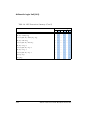
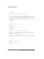
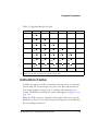
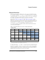
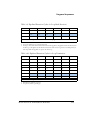
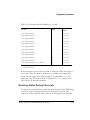
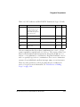
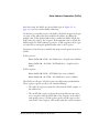
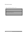
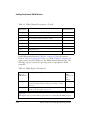
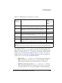
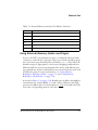
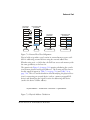
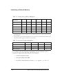
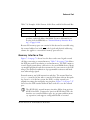
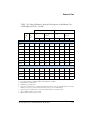
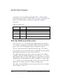
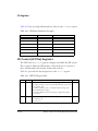
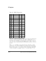
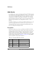
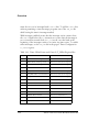
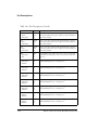
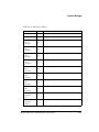
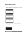
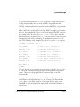
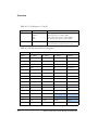
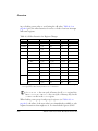
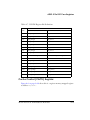
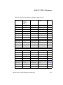
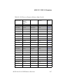
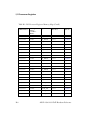
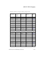
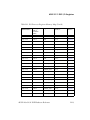
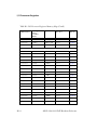
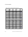
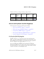
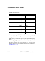
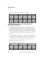
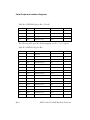
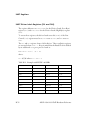
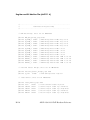
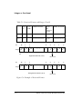
Table 6-2. DMA Register Descriptions (Cont’d)
DMA Register
Name (in
I/O Memory)
DMA Register Description
Order of
DMA
Descriptor (in
Data
Memory)
xxxx_SRP
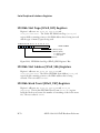
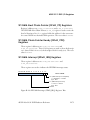
Start Page. Contains the Memory Space (MS) bit (bit 8, 0=memory, 1=boot) and transfer memory page (MP) bits (bits 7–0);
HEAD+1
xxxx_SRA
Start Address. Contains the 16-bit starting memory address of
transfer
HEAD+2
xxxx_CNT
DMA Count. Contains the 16-bit number of words in the transfer
HEAD+3
xxxx_CP
Next Descriptor Pointer. Contains the 16-bit memory address of
the Head of the next DMA descriptor
HEAD+4
xxxx_CPR
Descriptor Ready. Contains the Descriptor Ready (DR) bit (bit 0)
xxxx_IRQ
DMA Interrupt Status. Contains the DMA Complete Interrupt
Pending (DCOMI) bit (bit 0) and DMA Error Interrupt Pending
(DERI) bit (bit 1); 1=pending interrupt, 0=no interrupt
The xxxx in the register name corresponds to the DMA channels that are listed in Table 6-1 on
page 6-17.
The empty descriptor positions indicate registers that are not loaded from the DMA descriptor.
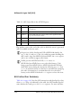
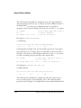
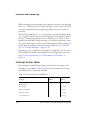
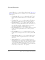
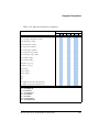
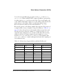
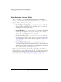
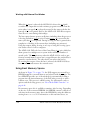
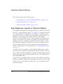
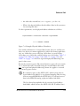
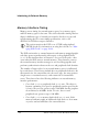
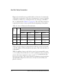
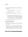
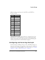
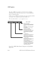
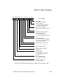
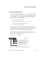
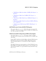
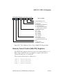
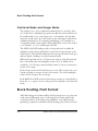
Each DMA channel’s xxxx_CFG register contains the following bits. Note
that some bits are read-only in registers and only can be loaded when the
DMA controller loads the xxxx_CFG register on descriptor load from data
memory (see “Descriptor-Based DMA Transfers” on page 6-11). Also, a
number of bits are read-only on channels where they are not supported
(such as the DAUTO bit on the memDMA channel):
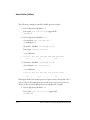
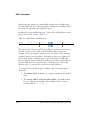
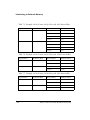
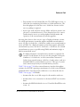
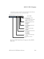
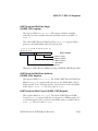
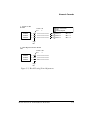
• DMA Enable. xxxx_CFG bit 0 (DEN). This bit directs the channel’s
DMA controller to start (if set, =1) or stop (if cleared, =0) the
DMA transfer defined by the DMA descriptor. (read/write)
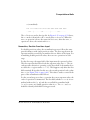
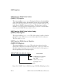
• DMA Transfer Direction Select. xxxx_CFG bit 1 (TRAN). This bit
selects the transfer direction as memory write (if set, =1) or memory read (if cleared, =0). (read-only; applies on all I/O channels)
ADSP-219x/2191 DSP Hardware Reference
6-19