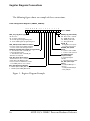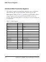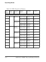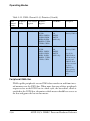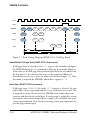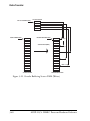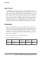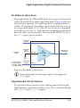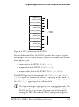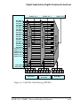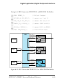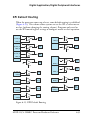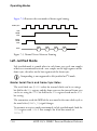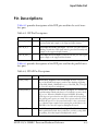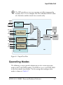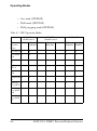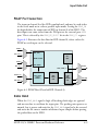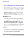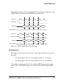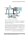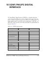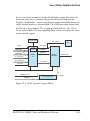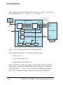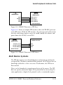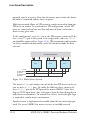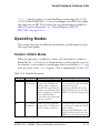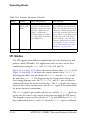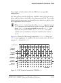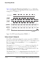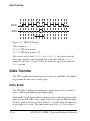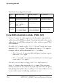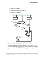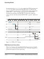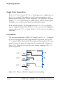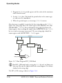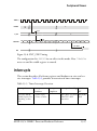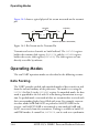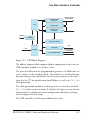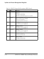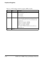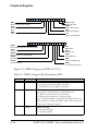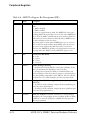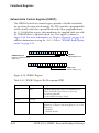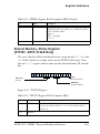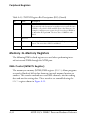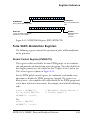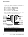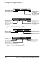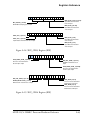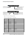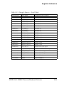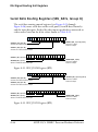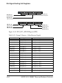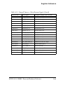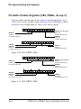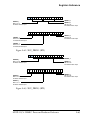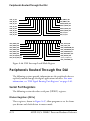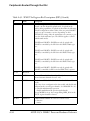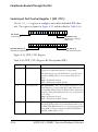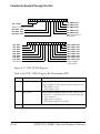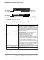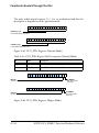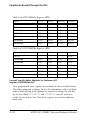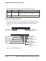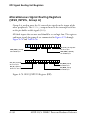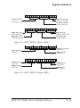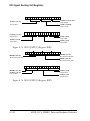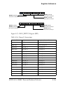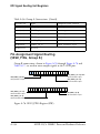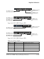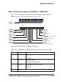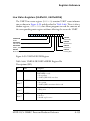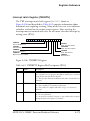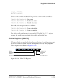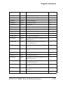
1
ADSP-2137x SHARC® Processor Hardware Reference Includes ADSP-21367, ADSP-21368, ADSP-21369, ADSP-21371, ADSP-21375 Revision 2.2, April 2013 Part Number 82-000100-01 Analog Devices, Inc. One Technology Way Norwood, Mass. 02062-9106 a Copyright Information © 2013 Analog Devices, Inc., ALL RIGHTS RESERVED. This document may not be reproduced in any form without prior, express written consent from Analog Devices, Inc. Printed in the USA. Disclaimer Analog Devices, Inc. reserves the right to change this product without prior notice. Information furnished by Analog Devices is believed to be accurate and reliable. However, no responsibility is assumed by Analog Devices for its use; nor for any infringement of patents or other rights of third parties which may result from its use. No license is granted by implication or otherwise under the patent rights of Analog Devices, Inc. Trademark and Service Mark Notice The Analog Devices logo, Blackfin, SHARC, TigerSHARC, CrossCore, VisualDSP++, and EZ-KIT Lite are registered trademarks of Analog Devices, Inc. All other brand and product names are trademarks or service marks of their respective owners. Contents PREFACE Purpose of This Manual ................................................................. xlv Intended Audience ......................................................................... xlv Manual Contents .......................................................................... xlvi What’s New in This Manual .......................................................... xlix Technical Support ......................................................................... xlix Supported Processors ......................................................................... l Product Information ......................................................................... l Analog Devices Web Site ............................................................ li EngineerZone ............................................................................. li Notation Conventions ..................................................................... lii Register Diagram Conventions ....................................................... liii INTRODUCTION Design Advantages ........................................................................ 1-1 SHARC Family Product Offerings ........................................... 1-2 ADSP-2137x SHARC Processor Hardware Reference iii Contents Processor Architectural Overview .................................................. 1-3 Processor Core ........................................................................ 1-3 I/O Peripherals ....................................................................... 1-3 I/O Processor ..................................................................... 1-3 Digital Audio Interface (DAI) ............................................. 1-4 Interrupt Controller ........................................................... 1-4 Signal Routing Unit ............................................................ 1-4 Digital Peripheral Interface (DPI) ....................................... 1-5 Interrupt Controller ........................................................... 1-5 Signal Routing Unit 2 ......................................................... 1-5 Development Tools ....................................................................... 1-6 Differences from Previous Processors ............................................. 1-7 I/O Architecture Enhancements .............................................. 1-7 I/O PROCESSOR Features ........................................................................................ 2-2 Register Overview ......................................................................... 2-3 DMA Channel Registers ............................................................... 2-3 DMA Channel Allocation ....................................................... 2-3 Standard DMA Parameter Registers ......................................... 2-4 Extended DMA Parameter Registers ........................................ 2-7 Data Buffers ........................................................................... 2-8 Chain Pointer Registers ......................................................... 2-10 iv ADSP-2137x SHARC Processor Hardware Reference Contents TCB Storage ............................................................................... 2-11 Serial Port TCB ..................................................................... 2-11 SPI TCB ............................................................................... 2-11 UART TCB .......................................................................... 2-12 External Port TCB ................................................................. 2-12 Clocking ..................................................................................... 2-17 Functional Description ............................................................... 2-17 Automated Data Transfer ....................................................... 2-17 DMA Transfer Types ............................................................. 2-18 DMA Direction ..................................................................... 2-19 Internal to External Memory ............................................. 2-19 Peripheral to Internal Memory .......................................... 2-20 Internal Memory to Internal Memory ................................ 2-20 DMA Controller Addressing .................................................. 2-20 Internal Index Register Addressing ..................................... 2-22 External Index Register Addressing .................................... 2-23 DMA Channel Status ............................................................ 2-23 DMA Start and Stop Conditions ............................................ 2-24 Operating Modes ........................................................................ 2-25 DMA Chaining ..................................................................... 2-27 TCB Memory Storage ....................................................... 2-27 Chain Assignment ............................................................. 2-28 Starting Chain Loading ..................................................... 2-30 ADSP-2137x SHARC Processor Hardware Reference v Contents TCB Chain Loading Priority ............................................. 2-31 Chain Insert Mode (SPORTs Only) .................................. 2-31 Fixed DMA Channel Arbitration ........................................... 2-31 Peripheral DMA Bus ......................................................... 2-36 External Port DMA Bus .................................................... 2-37 Rotating DMA Channel Arbitration ...................................... 2-37 Rotating Priority by Group ............................................... 2-38 Interrupts ................................................................................... 2-38 Sources ................................................................................. 2-39 Unchained DMA Interrupts .............................................. 2-39 Chained DMA Interrupts ................................................. 2-39 Transfer Completion Types .................................................... 2-40 Internal Transfer Completion ............................................ 2-40 Access Completion ........................................................... 2-41 Core Single Word Transfer Interrupts .................................... 2-41 Interrupt Versus Channel Priorities ........................................ 2-41 Debug Features ........................................................................... 2-42 Emulation Considerations ..................................................... 2-43 Effect Latency ............................................................................ 2-43 Write Effect Latency ............................................................. 2-43 IOP Effect Latency ............................................................... 2-43 IOP Throughput .................................................................. 2-43 Programming Model ................................................................... 2-44 General Procedure for Configuring DMA .............................. 2-44 vi ADSP-2137x SHARC Processor Hardware Reference Contents EXTERNAL PORT Features ........................................................................................ 3-2 Pin Descriptions ........................................................................... 3-4 Pin Multiplexing ..................................................................... 3-4 Register Overview ......................................................................... 3-4 Clocking ....................................................................................... 3-5 Functional Description ................................................................. 3-6 External Port Arbitration ......................................................... 3-7 External Port Bus Arbitration Conflicts ............................... 3-8 Channel Freezing ..................................................................... 3-8 Asynchronous Memory Interface ................................................... 3-8 AMI Features .......................................................................... 3-9 Functional Description ............................................................ 3-9 Asynchronous Reads ......................................................... 3-10 Asynchronous Writes ......................................................... 3-11 Parameter Timing ............................................................. 3-12 Idle Cycles ........................................................................ 3-12 Address Mapping .............................................................. 3-12 Operating Modes ................................................................... 3-13 Data Packing .................................................................... 3-13 External Access Extension .................................................. 3-14 Predictive Reads ................................................................ 3-15 ADSP-2137x SHARC Processor Hardware Reference vii Contents SDRAM Controller .................................................................... 3-16 Features ................................................................................ 3-16 Functional Description ......................................................... 3-17 SDRAM Commands ........................................................ 3-18 Load Mode Register ...................................................... 3-19 Single Bank Activation .................................................. 3-20 Multibank Activation (ADSP-2137x Processors) ............ 3-21 Single Precharge (ADSP-2137x Processors) .................... 3-21 Precharge All ................................................................ 3-21 Read/Write ................................................................... 3-21 Read/Write Full Page Burst (ADSP-2137x Processors) ... 3-24 Burst Stop (ADSP-2137x Processors) ............................ 3-24 Auto-Refresh ................................................................ 3-25 No Operation/Command Inhibit .................................. 3-25 Command Truth Table ................................................. 3-25 Address Mapping .............................................................. 3-26 External Addressing Modes ........................................... 3-27 Refresh Rate Control ........................................................ 3-32 Internal SDRAM Bank Access ........................................... 3-34 Single Bank Access ........................................................ 3-34 Multibank Access (ADSP-2137x Processors) .................. 3-34 Multi Bank Operation with Data Packing (ADSP-2137x) ........................................................... 3-36 Timing Parameters ............................................................ 3-36 Fixed Timing Parameters ............................................... 3-37 viii ADSP-2137x SHARC Processor Hardware Reference Contents Data Mask (DQM) ........................................................... 3-37 Resetting the Controller .................................................... 3-37 Operating Modes ................................................................... 3-38 Parallel Connection of SDRAMs ....................................... 3-38 Buffering Controller for Multiple SDRAMs ................... 3-39 SDRAM Read Optimization ............................................. 3-41 Core Accesses ................................................................ 3-42 DMA Access ................................................................. 3-43 Notes on Read Optimization ......................................... 3-43 Self-Refresh Mode ............................................................. 3-44 Forcing SDRAM Commands ............................................. 3-45 Force Precharge All ....................................................... 3-45 Force Load Mode Register (ADSP-2137x Only) ............. 3-46 Force Auto-Refresh ........................................................ 3-46 Shared Memory Interface (ADSP-21368) .................................... 3-46 Pin Descriptions .................................................................... 3-48 Functional Description .......................................................... 3-48 Bus Arbitration Protocol ................................................... 3-48 Bus Synchronization After Reset ........................................ 3-53 Shared AMI Protocol ........................................................ 3-55 Shared SDRAM Protocol .................................................. 3-55 Operating Modes ................................................................... 3-56 Rotating Priority Bus Arbitration (RPBA) .......................... 3-56 Bus Mastership Time-Out ................................................. 3-57 ADSP-2137x SHARC Processor Hardware Reference ix Contents Data Transfer ............................................................................. 3-58 Data Buffers ......................................................................... 3-59 Receive Buffer .................................................................. 3-59 Transmit Buffer ................................................................ 3-59 Core Access ........................................................................... 3-60 External Port Dual Data Fetch .......................................... 3-60 Conditional Instructions ................................................... 3-60 External Instruction Fetch (ADSP-2137x) ......................... 3-61 Fetching Instructions From External Memory ................ 3-61 External Port DMA Transfers ................................................ 3-70 External Port DMA Parameter Registers ............................ 3-71 Operating Modes .............................................................. 3-73 Internal DMA Addressing ............................................. 3-73 Standard DMA ............................................................. 3-73 Circular Buffered DMA ................................................ 3-74 Chained DMA Mode ........................................................ 3-75 Changing DMA Direction on the Fly (ADSP-2137x) .... 3-75 Scatter/Gather DMA (ADSP-2137x) ................................. 3-76 External Address Calculation ......................................... 3-77 Delay Line DMA .............................................................. 3-81 External Address Calculation for Reads ......................... 3-83 x ADSP-2137x SHARC Processor Hardware Reference Contents Interrupts ................................................................................... 3-85 Access Completion (ADSP-2137x) ......................................... 3-85 Internal Transfer Completion ................................................. 3-86 Interrupt Dependency on DMA Mode ................................... 3-86 External Port Throughput ........................................................... 3-87 AMI Data Throughput .......................................................... 3-87 SDRAM Throughput ............................................................ 3-87 Throughput Conditional Instructions ................................ 3-88 External Instruction Fetch Throughput (ADSP-2137x) .......... 3-88 Effect Latency ............................................................................. 3-90 Shared Memory ..................................................................... 3-90 Write Effect Latency .............................................................. 3-90 Programming Models .................................................................. 3-90 External Port ......................................................................... 3-91 AMI Initialization ............................................................. 3-91 DMA .................................................................................... 3-91 Standard DMA (ADSP-21367/8/9) ................................... 3-92 Chained DMA (ADSP-21367/8/9) .................................... 3-93 Standard DMA (ADSP-21371/5) ...................................... 3-94 Chained DMA (ADSP-21371/5) ....................................... 3-95 Delay Line DMA .............................................................. 3-96 Disabling and Re-enabling DMA ....................................... 3-96 Additional Information ..................................................... 3-97 ADSP-2137x SHARC Processor Hardware Reference xi Contents SDRAM Controller ............................................................... 3-98 Power-Up Sequence .......................................................... 3-98 Output Clock Generator Programming Model .................. 3-99 Self-Refresh Mode .......................................................... 3-100 Changing the VCO Clock During Runtime .................... 3-100 Bus Synchronization with Shared SDRAM ...................... 3-101 Bus Synchronization Notes ............................................. 3-103 Conditional Bus Master Instruction ................................ 3-104 External Instruction Fetch ................................................... 3-104 AMI Configuration ........................................................ 3-104 SDRAM Configuration .................................................. 3-104 External Memory Access Restrictions ................................... 3-105 ADSP-21367/8/9 Only ................................................... 3-105 ADSP-2137x Only ......................................................... 3-106 MEMORY-TO-MEMORY PORT DMA Features ........................................................................................ 4-2 Register Overview ......................................................................... 4-2 Clocking ...................................................................................... 4-2 Functional Description ................................................................. 4-3 Data Transfer ............................................................................... 4-3 Data Buffer ............................................................................. 4-3 DMA Transfer ........................................................................ 4-4 Interrupts ..................................................................................... 4-4 MTM Throughput ....................................................................... 4-5 xii ADSP-2137x SHARC Processor Hardware Reference Contents Effect Latency ............................................................................... 4-5 Write Effect Latency ................................................................ 4-5 MTM Effect Latency ............................................................... 4-5 Programming Model ..................................................................... 4-5 PULSE WIDTH MODULATION Features ........................................................................................ 5-2 Pin Descriptions ........................................................................... 5-4 Multiplexing Scheme ............................................................... 5-4 Register Overview ......................................................................... 5-5 Clocking ....................................................................................... 5-6 Functional Description ................................................................. 5-6 Two-Phase PWM Generator .................................................... 5-6 Switching Frequencies ......................................................... 5-6 Duty Cycles ........................................................................ 5-7 Dead Time ....................................................................... 5-12 Output Control Unit ............................................................. 5-12 Output Enable .................................................................. 5-13 Output Polarity ................................................................. 5-13 Complementary Outputs .................................................. 5-13 Crossover .......................................................................... 5-13 Emergency Dead Time for Over Modulation .......................... 5-14 Output Control Feature Precedence ................................... 5-16 ADSP-2137x SHARC Processor Hardware Reference xiii Contents Operating Modes ........................................................................ 5-17 Waveform Modes .................................................................. 5-17 Edge-Aligned Mode .......................................................... 5-17 Center-Aligned Mode ....................................................... 5-18 PWM Timer Edge Aligned Update ........................................ 5-20 Single Update Mode ......................................................... 5-21 Double Update Mode ....................................................... 5-22 Effective Accuracy ................................................................. 5-23 Synchronization of PWM Groups .......................................... 5-24 Interrupts ................................................................................... 5-24 Debug Features ........................................................................... 5-26 Status Debug Register ........................................................... 5-26 Emulation Considerations ..................................................... 5-26 Effect Latency ............................................................................ 5-27 Write Effect Latency ............................................................. 5-27 PWM Effect Latency ............................................................. 5-27 DIGITAL APPLICATION/DIGITAL PERIPHERAL INTERFACES Features ........................................................................................ 6-2 Register Overview ......................................................................... 6-3 Clocking ...................................................................................... 6-4 Functional Description ................................................................. 6-4 DAI/DPI Signal Naming Conventions ..................................... 6-7 I/O Pin Buffers ....................................................................... 6-7 xiv ADSP-2137x SHARC Processor Hardware Reference Contents Pin Buffers as Signal Output ............................................... 6-8 Pin Buffers as Signal Input ................................................ 6-10 Pin Buffers as Open Drain ................................................ 6-11 Programmable Pull-Up Resistors ........................................ 6-11 DAI/DPI Pin Buffer Status ................................................ 6-12 Unused DAI/DPI Pins ...................................................... 6-12 Miscellaneous Buffers ............................................................ 6-12 DAI/DPI Peripherals ............................................................. 6-14 Output Signals With Pin Buffer Enable Control ................ 6-14 Output Signals Without Pin Buffer Enable Control ........... 6-16 Signal Routing Units (SRUs) ................................................. 6-16 Signal Routing Matrix by Groups ...................................... 6-16 DAI/DPI Group Routing .................................................. 6-18 Rules for SRU Connections ............................................... 6-20 Making SRU Connections ................................................. 6-20 DAI Routing Capabilities .................................................. 6-24 DPI Routing Capabilities .................................................. 6-25 Pin Buffer Input ............................................................ 6-26 Pin Buffer Enable .......................................................... 6-26 Miscellaneous Signals .................................................... 6-27 DAI Default Routing ............................................................. 6-28 DPI Default Routing ............................................................. 6-31 Interrupts ................................................................................... 6-32 System versus Exception Interrupts ........................................ 6-32 ADSP-2137x SHARC Processor Hardware Reference xv Contents Functional Description ......................................................... 6-33 DAI Interrupt Channels ........................................................ 6-33 DAI Interrupt Priorities ........................................................ 6-34 DPI Interrupt Channels ........................................................ 6-34 DPI Interrupt Priorities ......................................................... 6-34 DAI Miscellaneous Interrupts ................................................ 6-35 DPI Miscellaneous Interrupts ................................................ 6-35 DAI/DPI Interrupt Mask Events ........................................... 6-36 DAI Interrupt Acknowledge .................................................. 6-38 DPI Interrupt Acknowledge .................................................. 6-39 Core Versus DAI/DPI Interrupts ........................................... 6-39 Debug Features ........................................................................... 6-40 DAI Shadow Registers ........................................................... 6-40 DPI Shadow Registers ........................................................... 6-40 Loop Back Routing ............................................................... 6-40 Effect Latency ............................................................................ 6-42 Write Effect Latency ............................................................. 6-42 Signal Routing Unit Effect Latency ........................................ 6-42 Programming Model ................................................................... 6-42 DAI Example System ............................................................ 6-43 SERIAL PORTS Features ........................................................................................ 7-2 Pin Descriptions ........................................................................... 7-4 xvi ADSP-2137x SHARC Processor Hardware Reference Contents SRU Programming ........................................................................ 7-5 SRU SPORT Receive Master ................................................... 7-6 SRU SPORT Signal Integrity ................................................... 7-6 Register Overview ......................................................................... 7-7 Clocking ....................................................................................... 7-8 Master Clock ........................................................................... 7-9 Master Frame Sync .................................................................. 7-9 Slave Mode ............................................................................ 7-10 Functional Description ............................................................... 7-11 Architecture .......................................................................... 7-11 Data Types and Companding ................................................. 7-12 Companding the Data Stream ........................................... 7-14 Transmit Path ................................................................... 7-15 Receive Path ..................................................................... 7-15 Frame Sync ........................................................................... 7-16 Frame Sync and Data Sampling ......................................... 7-16 Serial Word Length ........................................................... 7-17 Internal Versus External Frame Syncs ................................. 7-18 External Frame Sync Sampling ...................................... 7-19 Logic Level Frame Syncs ................................................ 7-19 Data-Independent Frame Sync ...................................... 7-20 Operating Modes ........................................................................ 7-20 Mode Selection ...................................................................... 7-22 Channel Order First .......................................................... 7-24 ADSP-2137x SHARC Processor Hardware Reference xvii Contents Standard Serial Mode ............................................................ 7-24 Timing Control Bits ......................................................... 7-24 Clocking Options ............................................................. 7-25 Frame Sync Options ......................................................... 7-25 Framed Versus Unframed Frame Syncs .............................. 7-25 Early Versus Late Frame Syncs .......................................... 7-26 Left-Justified Mode ............................................................... 7-28 Master Serial Clock and Frame Sync Rates ........................ 7-28 Timing Control Bits ......................................................... 7-29 I2S Mode .............................................................................. 7-29 Master Serial Clock and Frame Sync Rates ........................ 7-29 I2S Compatibility ............................................................. 7-30 Timing Control Bits ......................................................... 7-30 Multichannel Mode .............................................................. 7-31 Clocking Options ............................................................. 7-31 Frame Sync Options ......................................................... 7-32 Frame Sync Delay (MFD) ................................................. 7-32 Transmit Data Valid Signal ............................................... 7-33 Transmit Data Valid Output ......................................... 7-34 Timing Control Bits ......................................................... 7-35 Number of Channels (NCH) ............................................ 7-35 xviii ADSP-2137x SHARC Processor Hardware Reference Contents Packed Mode ......................................................................... 7-36 Clocking Options ............................................................. 7-37 Frame Sync Options .......................................................... 7-37 Timing Control Bits .......................................................... 7-37 Active Channel Selection Registers ......................................... 7-38 Transmit Selection Registers .............................................. 7-38 Receive Selection Registers ................................................ 7-39 Companding Selection ...................................................... 7-39 Companding Limitations .................................................. 7-39 Data Transfer Types .................................................................... 7-40 Data Buffers .......................................................................... 7-40 Transmit Buffers (TXSPxA/B) ........................................... 7-41 Receive Buffers (RXSPxA/B) ............................................. 7-41 Buffer Status ..................................................................... 7-41 Data Buffer Packing .......................................................... 7-43 Core Transfers ....................................................................... 7-43 Single Word Transfers ....................................................... 7-43 Frame Sync Generation ..................................................... 7-44 Internal Memory DMA Transfers ........................................... 7-45 Standard DMA ................................................................. 7-46 DMA Chaining ................................................................. 7-47 DMA Chain Insertion Mode ............................................. 7-48 Frame Sync Generation ..................................................... 7-49 ADSP-2137x SHARC Processor Hardware Reference xix Contents Interrupts ................................................................................... 7-49 Internal Transfer Completion ................................................ 7-50 Shared Channels ................................................................... 7-51 Error Detection ..................................................................... 7-51 Error Status .......................................................................... 7-53 Debug Features ........................................................................... 7-54 SPORT Loopback ................................................................. 7-54 LoopBack Routing ............................................................ 7-54 Buffer Hang Disable (BHD) .................................................. 7-54 Effect Latency ............................................................................ 7-55 Write Effect Latency ............................................................. 7-55 SPORT Effect Latency .......................................................... 7-55 Programming Model ................................................................... 7-55 Setting Up and Starting DMA Master Mode .......................... 7-56 Setting Up and Starting Chained DMA ................................. 7-56 Enter DMA Chain Insertion Mode ........................................ 7-57 Setting Up and Starting Multichannel Mode .......................... 7-57 Multichannel Mode Backward Compatibility .................... 7-58 Programming Packed Mode ................................................... 7-59 Additional Information for External Frame Sync Operation ........................................................ 7-60 Companding As a Function ................................................... 7-60 INPUT DATA PORT Features ........................................................................................ 8-2 xx ADSP-2137x SHARC Processor Hardware Reference Contents Pin Descriptions ........................................................................... 8-3 SRU Programming ........................................................................ 8-4 Register Overview ......................................................................... 8-5 Clocking ....................................................................................... 8-6 Functional Description ................................................................. 8-6 Operating Modes .......................................................................... 8-7 PDAP Port Selection ............................................................... 8-9 Data Hold ............................................................................... 8-9 PDAP Data Masking ............................................................. 8-10 PDAP Data Packing .............................................................. 8-10 No Packing ....................................................................... 8-10 Packing by 2 ..................................................................... 8-11 Packing by 3 ..................................................................... 8-12 Packing by 4 ..................................................................... 8-13 Data Transfer .............................................................................. 8-14 Data Buffer ........................................................................... 8-14 Core Transfers ....................................................................... 8-15 SIP Data Buffer Format ..................................................... 8-16 PDAP Data Buffer Format ................................................ 8-18 DMA Transfers ...................................................................... 8-19 Data Buffer Format for DMA ............................................ 8-19 DMA Channel Priority ..................................................... 8-20 Standard DMA ................................................................. 8-20 Ping-Pong DMA ............................................................... 8-21 ADSP-2137x SHARC Processor Hardware Reference xxi Contents Multichannel DMA Operation ......................................... 8-21 Multichannel FIFO Status ................................................ 8-22 Interrupts ................................................................................... 8-23 Interrupt Acknowledge .......................................................... 8-23 Threshold Interrupts ............................................................. 8-23 DMA Interrupts .................................................................... 8-24 FIFO Overflow Interrupts ..................................................... 8-24 Debug Features ........................................................................... 8-25 Status Register Debug ........................................................... 8-25 Buffer Hang Disable ............................................................. 8-25 Shadow Registers .................................................................. 8-25 Core FIFO Write .................................................................. 8-26 Effect Latency ............................................................................ 8-26 Write Effect Latency ............................................................. 8-26 IDP Effect Latency ................................................................ 8-26 Programming Model ................................................................... 8-27 Setting Miscellaneous Bits ..................................................... 8-27 Starting Core Interrupt-Driven Transfer ................................ 8-27 Additional Notes .............................................................. 8-28 Starting A Standard DMA Transfer ........................................ 8-29 Starting a Ping-Pong DMA Transfer ...................................... 8-30 Servicing Interrupts for DMA ............................................... 8-31 ASYNCHRONOUS SAMPLE RATE CONVERTER Features ........................................................................................ 9-2 xxii ADSP-2137x SHARC Processor Hardware Reference Contents Pin Descriptions ........................................................................... 9-3 SRU Programming ........................................................................ 9-3 Register Overview ......................................................................... 9-4 Clocking ....................................................................................... 9-5 Functional Description ................................................................. 9-5 Operating Modes .......................................................................... 9-9 TDM Daisy Chain Mode ...................................................... 9-11 TDM Input Daisy Chain .................................................. 9-11 TDM Output Daisy Chain ............................................... 9-12 Bypass Mode ......................................................................... 9-12 Matched-Phase Mode ............................................................ 9-12 Data Format Matched-Phase Mode .................................... 9-14 Group Delay ..................................................................... 9-14 Decimation Rate ................................................................... 9-15 Muting Modes ....................................................................... 9-15 Soft Mute ......................................................................... 9-15 Hard Mute ........................................................................ 9-16 Auto Mute ........................................................................ 9-16 Interrupts ................................................................................... 9-16 Debug Features ........................................................................... 9-17 Effect Latency ............................................................................. 9-17 Write Effect Latency .............................................................. 9-17 SRC Effect Latency ............................................................... 9-18 ADSP-2137x SHARC Processor Hardware Reference xxiii Contents SONY/PHILIPS DIGITAL INTERFACE Features ...................................................................................... 10-2 Pin Descriptions ......................................................................... 10-3 SRU Programming ..................................................................... 10-5 Register Overview ....................................................................... 10-6 Clocking .................................................................................... 10-7 S/PDIF Transmitter .................................................................... 10-7 Functional Description ......................................................... 10-7 Input Data Format ......................................................... 10-10 Operating Modes ................................................................ 10-12 Full Serial Mode ............................................................. 10-12 Standalone Mode ............................................................ 10-12 Data Output Mode ......................................................... 10-13 S/PDIF Receiver ....................................................................... 10-14 Functional Description ....................................................... 10-14 Clock Recovery .............................................................. 10-16 Output Data Format ...................................................... 10-16 Channel Status ............................................................... 10-17 Operating Modes ................................................................ 10-17 Compressed or Non-linear Audio Data ............................ 10-17 Emphasized Audio Data .............................................. 10-18 Single-Channel Double-Frequency Mode .................... 10-19 xxiv ADSP-2137x SHARC Processor Hardware Reference Contents Clock Recovery Modes .................................................... 10-19 Digital On-Chip PLL .................................................. 10-19 External Analog PLL ................................................... 10-20 Interrupts ................................................................................. 10-20 Transmitter Interrupt ........................................................... 10-20 Receiver Interrupts .............................................................. 10-21 Receiver Error Interrupts ..................................................... 10-21 Debug Features ......................................................................... 10-22 Loop Back Routing .............................................................. 10-22 Effect Latency ........................................................................... 10-22 Write Effect Latency ............................................................ 10-22 S/PDIF Effect Latency ......................................................... 10-22 S/PDIF Transmit ............................................................ 10-22 S/PDIF Receive .............................................................. 10-23 Programming Model ................................................................. 10-23 Programming the Transmitter .............................................. 10-24 Programming the Receiver ................................................... 10-24 Interrupted Data Streams on the Receiver ............................ 10-25 PRECISION CLOCK GENERATOR Features ...................................................................................... 11-2 Pin Descriptions ......................................................................... 11-3 SRU Programming ...................................................................... 11-4 Register Overview ....................................................................... 11-5 Clocking ..................................................................................... 11-5 ADSP-2137x SHARC Processor Hardware Reference xxv Contents Functional Description ............................................................... 11-6 Serial Clock .......................................................................... 11-6 Frame Sync ........................................................................... 11-7 Frame Sync Output .......................................................... 11-7 Divider Mode Selection .................................................... 11-8 Phase Shift ....................................................................... 11-8 Pulse Width ..................................................................... 11-9 Default Pulse Width ....................................................... 11-10 Timing Example for I2S Mode ........................................ 11-10 Operating Modes ...................................................................... 11-11 Normal Mode ..................................................................... 11-11 Bypass Mode ....................................................................... 11-12 One-Shot Mode .................................................................. 11-13 External Event Trigger ......................................................... 11-14 External Event Trigger Delay .......................................... 11-15 Audio System Example ........................................................ 11-15 Clock Configuration Examples ............................................ 11-17 Effect Latency .......................................................................... 11-18 Write Effect Latency ........................................................... 11-18 PCG Effect Latency ............................................................ 11-19 Programming Model ................................................................. 11-19 Frame Sync Phase Setting .................................................... 11-20 External Event Trigger ......................................................... 11-20 Debug Features ......................................................................... 11-21 xxvi ADSP-2137x SHARC Processor Hardware Reference Contents SERIAL PERIPHERAL INTERFACE PORTS Features ...................................................................................... 12-2 Pin Descriptions ......................................................................... 12-3 SRU Programming ...................................................................... 12-4 Register Overview ....................................................................... 12-6 Clocking ..................................................................................... 12-6 Choosing the Pin Enable for the SPI Clock ............................ 12-7 Functional Description ............................................................... 12-8 Single Master Systems .......................................................... 12-10 Multi Master Systems .......................................................... 12-11 Operating Modes ...................................................................... 12-13 Transfer Initiate Mode ......................................................... 12-13 SPI Modes ........................................................................... 12-14 Slave Select Outputs ............................................................ 12-16 Frame Delay for Slave .......................................................... 12-17 Data Transfer ............................................................................ 12-18 Data Buffer ......................................................................... 12-18 Core Transfers ..................................................................... 12-19 DMA Transfers .................................................................... 12-20 Slave DMA Transfer Preparation ..................................... 12-21 SPI DMA Chaining ........................................................ 12-22 Setting Up and Starting Chained DMA ....................... 12-22 ADSP-2137x SHARC Processor Hardware Reference xxvii Contents Core and DMA Transfers .................................................... 12-23 Changing SPI Configuration ........................................... 12-23 Starting and Stopping SPI Data Transfers ........................ 12-24 Interrupts ................................................................................. 12-25 Interrupt Sources ................................................................ 12-26 Internal Transfer Completion .......................................... 12-27 Multi Master Error .............................................................. 12-27 Debug Features ......................................................................... 12-28 Shadow Receive Buffers ....................................................... 12-29 Internal Loopback Mode ..................................................... 12-29 Loop Back Routing ......................................................... 12-29 Effect Latency .......................................................................... 12-30 Write Effect Latency ........................................................... 12-30 SPI Effect Latency ............................................................... 12-30 Programming Model ................................................................. 12-30 Master Mode Core Transfers ................................................ 12-30 Multimaster Transfers ..................................................... 12-32 Slave Mode Core Transfers .................................................. 12-32 Master Mode DMA Transfers .............................................. 12-34 Slave Mode DMA Transfers ................................................. 12-35 Chained DMA Transfers ..................................................... 12-37 Stopping Core Transfers ...................................................... 12-37 Stopping DMA Transfers ..................................................... 12-38 Switching from Transmit To Transmit/Receive DMA ........... 12-39 xxviii ADSP-2137x SHARC Processor Hardware Reference Contents Switching from Receive to Receive/Transmit DMA ............... 12-40 DMA Error Interrupts ......................................................... 12-42 PERIPHERAL TIMERS Features ...................................................................................... 13-2 Pin Descriptions ......................................................................... 13-3 SRU Programming ...................................................................... 13-3 Register Overview ....................................................................... 13-4 Read-Modify-Write ............................................................... 13-5 Clocking ..................................................................................... 13-5 Functional Description ............................................................... 13-6 Operating Modes ........................................................................ 13-7 Pulse Width Modulation Mode (PWM_OUT) ....................... 13-8 PWM Waveform Generation ........................................... 13-10 Single-Pulse Generation .................................................. 13-12 Pulse Mode ..................................................................... 13-12 Pulse Width Count and Capture Mode (WDTH_CAP) ....... 13-13 External Event Watchdog Mode (EXT_CLK) ....................... 13-15 Interrupts ................................................................................. 13-17 Sources ................................................................................ 13-18 Watchdog Functionality ....................................................... 13-19 Debug Features ......................................................................... 13-19 Loop Back Routing .............................................................. 13-19 Emulation Considerations ................................................... 13-19 ADSP-2137x SHARC Processor Hardware Reference xxix Contents Effect Latency .......................................................................... 13-20 Write Effect Latency ........................................................... 13-20 Peripheral Timers Effect Latency ......................................... 13-20 Programming Model ................................................................. 13-20 PWM Out Mode ................................................................ 13-21 WDTH_CAP Mode ........................................................... 13-23 EXT_CLK Mode ................................................................ 13-24 UART PORT CONTROLLER Features ...................................................................................... 14-2 SRU Programming ..................................................................... 14-3 Register Overview ....................................................................... 14-3 Clocking .................................................................................... 14-4 Functional Description ............................................................... 14-6 Serial Communication .......................................................... 14-7 Operating Modes ........................................................................ 14-8 Data Packing ........................................................................ 14-8 9-Bit Transmission Mode ...................................................... 14-9 Packed Mode .................................................................. 14-10 Data Transfer ........................................................................... 14-10 Data Buffers ....................................................................... 14-11 Transmit Holding Registers (UARTxTHR) ..................... 14-11 Receive Buffer Registers (UARTxRBR) ............................ 14-12 Core Transfers ..................................................................... 14-13 xxx ADSP-2137x SHARC Processor Hardware Reference Contents DMA Transfers .................................................................... 14-14 DMA Chaining ............................................................... 14-15 Interrupts ................................................................................. 14-15 Interrupt Routing ................................................................ 14-16 DPI ................................................................................ 14-16 UART ............................................................................ 14-17 DMA Interrupts .................................................................. 14-17 Core Interrupts ................................................................... 14-18 Error Interrupts ................................................................... 14-20 Debug Features ......................................................................... 14-21 Shadow Registers ................................................................. 14-21 Shadow Buffer ..................................................................... 14-21 Loop Back Routing .............................................................. 14-21 Effect Latency ........................................................................... 14-21 Write Effect Latency ............................................................ 14-22 UART Effect Latency .......................................................... 14-22 Programming Model ................................................................. 14-22 Autobaud Detection ............................................................ 14-22 Programming Model for DMA Transfers .............................. 14-23 Setting Up and Starting Chained DMA ........................... 14-24 Notes on Using UART DMA .......................................... 14-24 Programming Model for Core Transfers ................................ 14-25 TWO-WIRE INTERFACE CONTROLLER Features ...................................................................................... 15-2 ADSP-2137x SHARC Processor Hardware Reference xxxi Contents Pin Descriptions ......................................................................... 15-3 SRU Programming ..................................................................... 15-4 Clocking .................................................................................... 15-4 Register Overview ....................................................................... 15-5 Functional Description ............................................................... 15-6 Bus Arbitration ..................................................................... 15-9 Start and Stop Conditions ................................................... 15-10 Slave Mode Addressing ........................................................ 15-11 Master Mode Addressing ..................................................... 15-11 Data Transfer ........................................................................... 15-11 Data Buffers ....................................................................... 15-11 8-Bit Transmit FIFO Register ......................................... 15-12 16-Bit Transmit FIFO Register ....................................... 15-12 8-Bit Receive FIFO Register ........................................... 15-13 16-Bit Receive FIFO Register .......................................... 15-13 Operating Modes ...................................................................... 15-14 General Call Addressing ...................................................... 15-14 Fast Mode ........................................................................... 15-15 Interrupts ................................................................................. 15-15 Interrupt Routing ............................................................... 15-16 DPI ................................................................................ 15-16 TWI .............................................................................. 15-16 Interrupt Sources ................................................................ 15-17 xxxii ADSP-2137x SHARC Processor Hardware Reference Contents Debug Features ......................................................................... 15-18 Buffer Hang Disable ............................................................ 15-18 Loop Back Routing .............................................................. 15-18 Effect Latency ........................................................................... 15-18 Write Effect Latency ............................................................ 15-19 TWI Effect Latency ............................................................. 15-19 Programming Model ................................................................. 15-19 General Setup ...................................................................... 15-19 Slave Mode .......................................................................... 15-20 Master Mode Clock Setup ................................................... 15-21 Master Mode Transmit ........................................................ 15-22 Master Mode Receive ........................................................... 15-23 Repeated Start Condition .................................................... 15-24 Transmit/Receive Repeated Start Sequence ....................... 15-25 Receive/Transmit Repeated Start Sequence ....................... 15-26 Electrical Specifications ............................................................. 15-27 POWER MANAGEMENT Features ...................................................................................... 16-1 Register Overview ....................................................................... 16-1 Phase-Locked Loop (PLL) ........................................................... 16-2 Functional Description .......................................................... 16-2 PLL Input Clock ................................................................... 16-3 Pre Divider Input .................................................................. 16-3 ADSP-2137x SHARC Processor Hardware Reference xxxiii Contents PLL Multiplier ...................................................................... 16-4 PLLM Hardware Control .................................................. 16-4 PLLM Software Control ................................................... 16-4 PLL VCO ............................................................................. 16-5 Output Clock Generator ....................................................... 16-6 Core Clock (CCLK) ........................................................ 16-6 IOP Clock (PCLK) ........................................................... 16-6 SDRAM Clock (SDCLK) ................................................. 16-6 Default PLL Hardware Settings ............................................. 16-7 Operating Modes ........................................................................ 16-7 Bypass Mode ......................................................................... 16-7 Normal Mode ....................................................................... 16-8 Clocking Golden Rules ......................................................... 16-8 Power-Up Sequence .................................................................... 16-8 PLL Start-Up ........................................................................ 16-9 Power Management .................................................................. 16-10 Peripherals .......................................................................... 16-10 DAI Routing Unit ............................................................... 16-10 External Port Control .......................................................... 16-11 Example for Clock Management ..................................... 16-11 General Notes on Power Savings ..................................... 16-12 xxxiv ADSP-2137x SHARC Processor Hardware Reference Contents Programming Model ................................................................. 16-12 Post Divider ........................................................................ 16-13 Multiplier and Post Divider Programming Model ................. 16-13 Back to Back Bypass ............................................................ 16-15 SYSTEM DESIGN Features ...................................................................................... 17-2 Pin Descriptions ......................................................................... 17-2 Register Overview ....................................................................... 17-2 Processor Reset ........................................................................... 17-3 Hardware Reset ..................................................................... 17-4 Software Reset ....................................................................... 17-4 Running Reset (ADSP-2137x Only) ...................................... 17-5 System Considerations ...................................................... 17-6 External Host ................................................................ 17-7 Processor Booting ....................................................................... 17-7 Boot Mechanisms .................................................................. 17-8 External Port Booting ............................................................ 17-8 SPI Port Booting ................................................................. 17-12 Master Boot Mode .......................................................... 17-13 Master Header Information ............................................. 17-14 Slave Boot Mode ............................................................. 17-16 ADSP-2137x SHARC Processor Hardware Reference xxxv Contents SPI Boot Packing ............................................................ 17-17 32-Bit SPI Packing ..................................................... 17-19 16-Bit SPI Packing ..................................................... 17-20 8-Bit SPI Packing ....................................................... 17-21 Kernel Boot Time ............................................................... 17-22 ROM Booting ..................................................................... 17-23 Programming Model ................................................................. 17-23 Running Reset .................................................................... 17-24 Running The Boot Kernel ................................................... 17-24 Loading the Boot Kernel Using DMA ............................. 17-24 Executing the Boot Kernel .............................................. 17-25 Loading the Application ................................................. 17-25 Loading the Application’s Interrupt Vector Table ............. 17-25 Starting Program Execution ............................................ 17-26 Memory Aliasing in Internal Memory .................................. 17-26 Pin Multiplexing ...................................................................... 17-27 Core FLAG Pins Multiplexing ............................................. 17-27 Backward Compatibility ................................................. 17-28 External Port Pin Multiplexing ............................................ 17-28 Multiplexed External Port Pins ........................................ 17-29 Backward Compatibility ................................................. 17-30 Parallel Connection of External Port and DPI Flag Pins ................................................................... 17-30 External Port Multiplexing Examples .............................. 17-32 xxxvi ADSP-2137x SHARC Processor Hardware Reference Contents High Frequency Design ............................................................. 17-33 Circuit Board Design ........................................................... 17-33 Clock Input Specifications and Jitter ............................... 17-33 RESETOUT ................................................................... 17-34 Input Pin Hysteresis ........................................................ 17-34 Pull-Up/Pull-Down Resistors ........................................... 17-35 Memory Select Pins ......................................................... 17-35 Edge Triggered I/O ......................................................... 17-36 Asynchronous Inputs ....................................................... 17-36 Decoupling and Grounding ................................................. 17-37 Circuit Board Layout ........................................................... 17-37 Other Recommendations and Suggestions ............................ 17-37 EZ-KIT Lite Schematics ...................................................... 17-39 Oscilloscope Probes ............................................................. 17-39 Recommended Reading ....................................................... 17-40 System Components ................................................................. 17-41 Supervisory Circuits ............................................................ 17-41 Definition of Terms .................................................................. 17-43 REGISTERS REFERENCE Overview ..................................................................................... A-2 Register Diagram Conventions ................................................ A-2 Bit Types and Settings ............................................................ A-3 ADSP-2137x SHARC Processor Hardware Reference xxxvii Contents System and Power Management Registers ...................................... A-4 System Control Register (SYSCTL) ......................................... A-4 Power Management Control Registers (PMCTL) ..................... A-7 Running Reset Control Register (RUNRSTCTL) ................... A-11 Peripheral Registers ..................................................................... A-11 External Port Registers .......................................................... A-11 Control Register (EPCTL) ................................................ A-12 ADSP-21367/8/9 External Port DMA Control Registers (DMACx) ....................................................... A-15 ADSP-2137x External Port DMA Control Registers (DMACx) A-17 AMI Control Registers (AMICTLx) .................................. A-21 AMI Status Register (AMISTAT) ...................................... A-24 SDRAM Registers ................................................................. A-25 Control Register (SDCTL) ............................................... A-25 Control Status Register (SDSTAT) .................................... A-29 Refresh Rate Control Register (SDRRC) ........................... A-30 Shared Memory Status Register (SYSTAT, ADSP-21368 Only) ............................................ A-31 Memory-to-Memory Registers ............................................... A-32 DMA Control (MTMCTL Register) ................................. A-32 Pulse Width Modulation Registers ......................................... A-33 Global Control Register (PWMGCTL) ............................. A-33 Global Status Register (PWMGSTAT) .............................. A-35 Control Register (PWMCTLx) ......................................... A-35 Status Registers (PWMSTATx) ......................................... A-37 xxxviii ADSP-2137x SHARC Processor Hardware Reference Contents Output Disable Registers (PWMSEGx) ............................ A-37 Polarity Select Registers (PWMPOLx) .............................. A-38 Period Registers (PWMPERIODx) ................................... A-39 Duty Cycle High Side Registers (PWMAx, PWMBx) ........ A-39 Duty Cycle Low Side Registers (PWMALx, PWMBLx) ..... A-40 Dead Time Registers (PWMDTx) .................................... A-40 Debug Status Registers (PWMDBGx) .............................. A-40 DAI Signal Routing Unit Registers ............................................. A-40 Clock Routing Control Registers (SRU_CLKx, Group A) ..................................................... A-41 Serial Data Routing Registers (SRU_DATx, Group B) ........... A-46 Frame Sync Routing Control Registers (SRU_FSx, Group C) ........................................................ A-51 Pin Signal Assignment Registers (SRU_PINx, Group D) ...................................................... A-55 Miscellaneous Signal Routing Registers (SRU_MISCx, Group E) ................................................... A-61 Pin Buffer Enable Registers (SRU_PBENx, Group F) ............ A-64 Pin Buffer Registers .............................................................. A-68 Pin Buffer Status Registers (DAI_PIN_STAT) .................. A-68 Resistor Pull-up Enable Register (DAI_PIN_PULLUP) ..... A-68 Interrupt Controller Registers ............................................... A-69 Peripherals Routed Through the DAI ......................................... A-70 Serial Port Registers .............................................................. A-70 Divisor Registers (DIVx) .................................................. A-70 ADSP-2137x SHARC Processor Hardware Reference xxxix Contents Serial Control Registers (SPCTLx) .................................... A-71 Multichannel Control Registers (SPMCTLx) ..................... A-87 Multichannel Active Channel Select Registers .................... A-91 Transmit Channel Select Registers (MTxCSy) ................ A-92 Transmit Channel Compand Select Registers (MTxCCSy) A-92 Receive Channel Select Registers (MRxCSy) .................. A-92 Receive Compand Channel Select Registers (MRxCCSy) A-93 Error Control Register (SPERRCTLx) ........................... A-93 Error Status Register (SPERRSTAT) .............................. A-95 Input Data Port Registers ...................................................... A-95 Serial Input Port Control Register 0 (IDP_CTL0) ............. A-95 Serial Input Port Control Register 1 (IDP_CTL1) ............. A-98 Parallel Data Acquisition Port Control Register (IDP_PP_CTL) ............................................................. A-99 Status Register (DAI_STAT0) ......................................... A-101 Status Debug Register 1 (DAI_STAT1) ........................... A-103 Sample Rate Converter Registers ......................................... A-104 Control Registers (SRCCTLx) ........................................ A-104 Mute Register (SRCMUTE) ........................................... A-108 Ratio Registers (SRCRATx) ............................................ A-109 Precision Clock Generator Registers .................................... A-111 Control Registers (PCG_CTLxy) .................................... A-111 Pulse Width Registers (PCG_PWx) ................................. A-113 Frame Synchronization Registers (PCG_SYNCx) ............ A-115 xl ADSP-2137x SHARC Processor Hardware Reference Sony/Philips Digital Interface Registers ............................... A-119 Transmitter Registers ...................................................... A-119 Transmit Control Register (DITCTL) ......................... A-119 Transmit Status Bit Registers for Subframe A/B (DITCHANAx/Bx) ................................................. A-121 Transmit User Bits Buffer Registers for Subframe A/B Registers (DITUSRBITAx/Bx) ................................. A-122 User Bit Update Register (DITUSRUPD) ................... A-123 Receiver Registers ........................................................... A-124 Receive Control Register (DIRCTL) ........................... A-124 Receive Status Register (DIRSTAT) ............................ A-126 Receive Status Registers for Subframe A (DIRCHANL) A-129 Receive Status Registers for Subframe B (DIRCHANR) A-129 DPI Signal Routing Unit Registers ........................................... A-129 Miscellaneous Signal Routing Registers (SRU2_INPUTx, Group A) ............................................. A-130 Pin Assignment Signal Routing (SRU2_PINx, Group B) ................................................. A-134 Pin Enable Signal Routing (SRU2_PBENx, Group C) .............................................. A-138 Pin Buffer Registers ............................................................ A-141 Pin Buffer Status Register (DPI_PIN_STAT) .................. A-142 Resistor Pull-up Enable Register (DPI_PIN_PULLUP) ... A-142 Interrupt Controller Registers ............................................. A-143 ADSP-2137x SHARC Processor Hardware Reference xli Peripherals Routed Through the DPI ........................................ A-144 Serial Peripheral Interface Registers ...................................... A-144 Control Registers (SPICTL, SPICTLB) ........................... A-144 DMA Configuration Registers (SPIDMAC, SPIDMACB) A-151 Baud Rate Registers (SPIBAUD, SPIBAUDB) ................. A-153 Status Registers (SPISTAT, SPISTATB) ........................... A-153 Flags Registers (SPIFLG, SPIFLGB) ................................ A-155 UART Control and Status Registers ..................................... A-157 Line Control Register (UARTxLCR) ............................... A-157 Line Status Registers (UARTxLSR, UARTxLSRSH) ........ A-159 Interrupt Enable Register (UARTxIER) ........................... A-160 Interrupt Identification Registers (UARTxIIR, UARTxIIRSH) .. A-161 Divisor Latch Registers (UARTxDLL, UARTxDLH) ....... A-163 Scratch Register (UARTxSCR) ........................................ A-163 Mode Register (UARTxMODE) ..................................... A-163 Buffer Control Registers (UARTxTXCTL, UARTxRXCTL) A-165 DMA Status Registers (UARTxTXSTAT, UARTxRXSTAT) A-166 Two-Wire Interface Registers ............................................... A-167 Master Internal Time Register (TWIMITR) .................... A-167 Clock Divider Register (TWIDIV) .................................. A-168 Slave Mode Control Register (TWISCTL) ...................... A-168 Slave Address Register (TWISADDR) ............................. A-170 Slave Status Register (TWISSTAT) .................................. A-170 Master Control Register (TWIMCTL) ............................ A-170 xlii ADSP-2137x SHARC Processor Hardware Reference Master Address Register (TWIMADDR) ........................ A-173 Master Mode Status Register (TWIMSTAT) ................... A-173 FIFO Control Register (TWIFIFOCTL) ........................ A-176 FIFO Status Register (TWIFIFOSTAT) ......................... A-177 Interrupt Latch Register (TWIIRPTL) ............................ A-179 Interrupt Mask Register (TWIIMASK) ........................... A-180 Peripheral Timer Registers .................................................. A-182 Read-Modify-Write Timer Control Register .................... A-182 Control Registers (TMxCTL) ......................................... A-183 Status Registers (TMxSTAT) .......................................... A-184 Register Listing ........................................................................ A-186 PERIPHERAL INTERRUPT CONTROL Interrupt Latency ......................................................................... B-1 Interrupt Acknowledge ................................................................. B-2 Interrupt Completion .................................................................. B-3 Interrupt Priority ......................................................................... B-4 Peripherals with Multiple Interrupt Vector Addresses ............... B-6 Priority Interrupt Control Registers (PICRx) ........................... B-7 AUDIO FRAME FORMATS Overview ..................................................................................... C-2 Standard Serial Mode ................................................................... C-2 I2S Mode ..................................................................................... C-3 Left-Justified Mode ...................................................................... C-5 ADSP-2137x SHARC Processor Hardware Reference xliii Right-Justified Mode .................................................................... C-5 TDM Mode ................................................................................. C-6 Packed TDM Mode ................................................................ C-7 MOST Mode .......................................................................... C-8 AES/EBU/SPDIF Formats ............................................................ C-9 Subframe Format .................................................................. C-12 Channel Coding ................................................................... C-14 Preambles ............................................................................. C-15 xliv ADSP-2137x SHARC Processor Hardware Reference PREFACE Thank you for purchasing and developing systems using ADSP-21367/8/9 and ADSP-21371/75 SHARC® processors from Analog Devices, Inc. Purpose of This Manual ADSP-2137x SHARC Processor Hardware Reference contains information about the peripheral set and I/O properties for the ADSP-21367/8/9 and ADSP-2137x processors. These are 32-bit, fixed- and floating-point digital signal processors from Analog Devices for use in computing, communications, and consumer applications. The manual provides information on the processor’s I/O architecture and the operation of the peripherals associated with each model. Intended Audience The primary audience for this manual is a programmer who is familiar with Analog Devices processors. The manual assumes the audience has a working knowledge of the appropriate processor architecture and instruction set. Programmers who are unfamiliar with Analog Devices processors can use this manual, but should supplement it with other texts, such as hardware and programming reference manuals that describe their target architecture. ADSP-2137x SHARC Processor Hardware Reference xlv Manual Contents Manual Contents This manual consists of: • Chapter 1, “Introduction” Provides an architectural overview of the ADSP-21367/8/9 and ADSP-2137/75 SHARC processors. • Chapter 2, “I/O Processor” Describes the input/output processor architecture, and provides direct memory access (DMA) procedures for the processor peripherals. • Chapter 3, “External Port” Describes how the processor’s on-chip DMA controller acts as a machine for transferring data without core interruption. • Chapter 4, “Memory-to-Memory Port DMA” The memory-to-memory port DMA module is used for internal memory transfers only. • Chapter 5, “Pulse Width Modulation” Describes the implementation and use of the pulse width modulation module which provides a technique for controlling analog circuits with the microprocessor’s digital outputs. • Chapter 6, “Digital Application/Digital Peripheral Interfaces” Provides information about the digital audio interface (DAI) which allows you to attach an arbitrary number and variety of peripherals to the processor while retaining high levels of compatibility. • Chapter 7, “Serial Ports” Describes the up to eight dual data line serial ports. Each SPORT contains a clock, a frame sync, and two data lines that can be configured as either a receiver or transmitter pair. xlvi ADSP-2137x SHARC Processor Hardware Reference Preface • Chapter 8, “Input Data Port” Discusses the function of the input data port (IDP) which provides a low overhead method of routing signal routing unit (SRU) signals back to the core’s memory. • Chapter 9, “Asynchronous Sample Rate Converter” Provides information on the sample rate converter (SRC) module. This module performs synchronous or asynchronous sample rate conversion across independent stereo channels, without using any internal processor resources. • Chapter 10, “Sony/Philips Digital Interface” Provides information on the use of the Sony/Philips Digital Interface which is a standard audio file transfer format that allows the transfer of digital audio signals from one device to another without having to be converted to an analog signal. • Chapter 11, “Precision Clock Generator” Details the precision clock generators (PCG), each of which generates a pair of signals derived from a clock input signal. • Chapter 12, “Serial Peripheral Interface Ports” Describes the operation of the serial peripheral interface (SPI) port. SPI devices communicate using a master-slave relationship and can achieve high data transfer rate because they can operate in full-duplex mode. • Chapter 13, “Peripheral Timers” In addition to the internal core timer, the processors contain identical 32-bit peripheral timers that can be used to interface with external devices. • Chapter 14, “UART Port Controller” Describes the operation of the Universal Asynchronous Receiver/Transmitter (UART) which is a full-duplex peripheral compatible with PC-style industry-standard UART. ADSP-2137x SHARC Processor Hardware Reference xlvii Manual Contents • Chapter 15, “Two-Wire Interface Controller” The two-wire interface is fully compatible with the widely used I2C bus standard. It is designed with a high level of functionality and is compatible with multimaster, multislave bus configurations. • Chapter 16, “Power Management” Contains information on managing the clock, PLL and the peripherals in order to maximize system efficiency with minimum power consumption. • Chapter 17, “System Design” Describes system design features of the SHARC processors. These, include resetting and booting the processor, as well as pin descriptions and other system-level information. • Appendix A, “Registers Reference” Provides a graphical presentation of all registers and describes the bit usage in each register. • Appendix B “Peripheral Interrupt Control” Provides a complete listing of the registers that are used to configure and control interrupts. • Appendix C “Audio Frame Formats” Provides specific information on all the serial timing protocols used for audio inter-chip communications. hardware reference is a companion document to the SHARC This Processor Programming Reference. The programming reference provides information relating to the processor core, such as processing elements, internal memory, and program sequencing. It also provides programming specific information, such as complete descriptions of the ADSP-21xxx instruction set and the compute operations, including their assembly language syntax and opcode fields. xlviii ADSP-2137x SHARC Processor Hardware Reference Preface What’s New in This Manual This manual is Revision 2.2 of ADSP-2137x SHARC Processor Hardware Reference for the ADSP-21362/3/4/5/6 Processors. This revision corrects minor typographical errors and the following issues: • TCB list for delay line DMA in Chapter 3, “External Port”. • Note on shared memory booting requirement in Chapter 3, “External Port”. • Corrected SPICLK baud rate expression in Appendix A, “Registers Reference”. Technical Support You can reach Analog Devices processors and DSP technical support in the following ways: • Post your questions in the processors and DSP support community at EngineerZone®: http://ez.analog.com/community/dsp • Submit your questions to technical support directly at: http://www.analog.com/support • E-mail your questions about processors, DSPs, and tools development software from CrossCore® Embedded Studio or VisualDSP++®: Choose Help > Email Support. This creates an e-mail to [email protected] and automatically attaches your CrossCore Embedded Studio or VisualDSP++ version information and license.dat file. ADSP-2137x SHARC Processor Hardware Reference xlix Supported Processors • E-mail your questions about processors and processor applications to: [email protected] or [email protected] (Greater China support) • In the USA only, call 1-800-ANALOGD (1-800-262-5643) • Contact your Analog Devices sales office or authorized distributor. Locate one at: www.analog.com/adi-sales • Send questions by mail to: Processors and DSP Technical Support Analog Devices, Inc. Three Technology Way P.O. Box 9106 Norwood, MA 02062-9106 USA Supported Processors The name “SHARC” refers to a family of high-performance, floating-point embedded processors. Refer to the CCES or VisualDSP++ online help for a complete list of supported processors. Product Information Product information can be obtained from the Analog Devices Web site and the CCES or VisualDSP++ online help. l ADSP-2137x SHARC Processor Hardware Reference Preface Analog Devices Web Site The Analog Devices Web site, www.analog.com, provides information about a broad range of products—analog integrated circuits, amplifiers, converters, and digital signal processors. To access a complete technical library for each processor family, go to http://www.analog.com/processors/technical_library. The manuals selection opens a list of current manuals related to the product as well as a link to the previous revisions of the manuals. When locating your manual title, note a possible errata check mark next to the title that leads to the current correction report against the manual. Also note, myAnalog is a free feature of the Analog Devices Web site that allows customization of a Web page to display only the latest information about products you are interested in. You can choose to receive weekly e-mail notifications containing updates to the Web pages that meet your interests, including documentation errata against all manuals. myAnalog provides access to books, application notes, data sheets, code examples, and more. Visit myAnalog to sign up. If you are a registered user, just log on. Your user name is your e-mail address. EngineerZone EngineerZone is a technical support forum from Analog Devices, Inc. It allows you direct access to ADI technical support engineers. You can search FAQs and technical information to get quick answers to your embedded processing and DSP design questions. Use EngineerZone to connect with other DSP developers who face similar design challenges. You can also use this open forum to share knowledge and collaborate with the ADI support team and your peers. Visit http://ez.analog.com to sign up. ADSP-2137x SHARC Processor Hardware Reference li Notation Conventions Notation Conventions Text conventions in this manual are identified and described as follows. lii Example Description File > Close Titles in reference sections indicate the location of an item within the IDE environment’s menu system (for example, the Close command appears on the File menu). {this | that} Alternative required items in syntax descriptions appear within curly brackets and separated by vertical bars; read the example as this or that. One or the other is required. [this | that] Optional items in syntax descriptions appear within brackets and separated by vertical bars; read the example as an optional this or that. [this,…] Optional item lists in syntax descriptions appear within brackets delimited by commas and terminated with an ellipsis; read the example as an optional comma-separated list of this. .SECTION Commands, directives, keywords, and feature names are in text with letter gothic font. filename Non-keyword placeholders appear in text with italic style format. Note: For correct operation, ... A Note provides supplementary information on a related topic. In the online version of this book, the word Note appears instead of this symbol. Caution: Incorrect device operation may result if ... Caution: Device damage may result if ... A Caution identifies conditions or inappropriate usage of the product that could lead to undesirable results or product damage. In the online version of this book, the word Caution appears instead of this symbol. Warning: Injury to device users may result if ... A Warning identifies conditions or inappropriate usage of the product that could lead to conditions that are potentially hazardous for devices users. In the online version of this book, the word Warning appears instead of this symbol. ADSP-2137x SHARC Processor Hardware Reference Preface Register Diagram Conventions Register diagrams use the following conventions: • The descriptive name of the register appears at the top, followed by the short form of the name in parentheses. • If the register is read-only (RO), write-1-to-set (W1S), or write-1-to-clear (W1C), this information appears under the name. Read/write is the default and is not noted. Additional descriptive text may follow. • If any bits in the register do not follow the overall read/write convention, this is noted in the bit description after the bit name. • If a bit has a short name, the short name appears first in the bit description, followed by the long name in parentheses. • The reset value appears in binary in the individual bits and in hexadecimal to the right of the register. • Bits marked x have an unknown reset value. Consequently, the reset value of registers that contain such bits is undefined or dependent on pin values at reset. • Shaded bits are reserved. upward compatibility with future implementations, Towriteensure back the value that is read for reserved bits in a register, unless otherwise specified. ADSP-2137x SHARC Processor Hardware Reference liii Register Diagram Conventions The following figure shows an example of these conventions. Timer Configuration Registers (TIMERx_CONFIG) 15 14 13 12 11 10 9 8 7 6 5 4 3 2 1 0 0 0 0 0 0 0 0 0 0 0 0 0 0 0 0 0 ERR_TYP[1:0] (Error Type) - RO 00 - No error. 01 - Counter overflow error. 10 - Period register programming error. 11 - Pulse width register programming error. EMU_RUN (Emulation Behavior Select) 0 - Timer counter stops during emulation. 1 - Timer counter runs during emulation. TOGGLE_HI (PWM_OUT PULSE_HI Toggle Mode) 0 - The effective state of PULSE_HI is the programmed state. 1 - The effective state of PULSE_HI alternates each period. CLK_SEL (Timer Clock Select) This bit must be set to 1, when operating the PPI in GP Output modes. 0 - Use system clock SCLK for counter. 1 - Use PWM_CLK to clock counter. OUT_DIS (Output Pad Disable) 0 - Enable pad in PWM_OUT mode. 1 - Disable pad in PWM_OUT mode. Reset = 0x0000 TMODE[1:0] (Timer Mode) 00 - Reset state - unused. 01 - PWM_OUT mode. 10 - WDTH_CAP mode. 11 - EXT_CLK mode. PULSE_HI 0 - Negative action pulse. 1 - Positive action pulse. PERIOD_CNT (Period Count) 0 - Count to end of width. 1 - Count to end of period. IRQ_ENA (Interrupt Request Enable) 0 - Interrupt request disable. 1 - Interrupt request enable TIN_SEL (Timer Input Select) 0 - Sample TMRx pin or PF1 pin. 1 - Sample UART RX pin or PPI_CLK pin. Figure 1. Register Diagram Example liv ADSP-2137x SHARC Processor Hardware Reference 1 INTRODUCTION The ADSP-21367/8/9 and ADSP-21371/75 SHARC processors are high performance 32-bit processors used for high quality audio, medical imaging, communications, military, test equipment, 3D graphics, speech recognition, motor control, imaging, and other applications. By adding on-chip SRAM, integrated I/O peripherals, and an additional processing element for single-instruction, multiple-data (SIMD) support, this processor builds on the ADSP-21000 family DSP core to form a complete system-on-a-chip. Design Advantages A digital signal processor’s data format determines its ability to handle signals of differing precision, dynamic range, and signal-to-noise ratios. Because floating-point DSP math reduces the need for scaling and the probability of overflow, using a floating-point processor can simplify algorithm and software development. The extent to which this is true depends on the floating-point processor’s architecture. Consistency with IEEE workstation simulations and the elimination of scaling are clearly two ease-of-use advantages. High level language programmability, large address spaces, and wide dynamic range allow system development time to be spent on algorithms and signal processing concerns, rather than assembly language coding, code paging, and/or error handling. The SHARC processors are highly integrated, 32-bit floating-point processor which provides all of these design advantages. ADSP-2137x SHARC Processor Hardware Reference 1-1 Design Advantages SHARC Family Product Offerings Table 1-1 provides information on the products covered in this manual. Note that some models are available for automotive applications with controlled manufacturing. These special models may have specifications that differ from the general release models. For information on which models are available as automotive, see the product-specific data sheet. Table 1-1. SHARC Processor Family Features Feature ADSP-21368 ADSP-213671 ADSP-21369 ADSP-21371 ADSP-21375 RAM 2M bit 1M bit 0.5M bit ROM 6M bit 4M bit 2M bit Audio Decoders in ROM2 Yes No Serial Ports 8 UART 2 Pulse Width Modulation SRC Performance Package Option3 Processor Speed 1 Yes S/PDIF Shared Memory 4 No Yes No No Yes 128 db 140 dB 256-ball BGA 256-ball BGA 208-lead LQFP, exposed pad 400 MHz No 128 dB 256-ball BGA 208-lead LQFP, exposed pad 128 dB No SRC 208-lead LQFP, exposed pad 266 MHz 1 The ADSP-21367 processor includes a customer-definable ROM block. Please contact your Analog Devices sales representative for additional details. 2 Audio decoding algorithms include PCM, Dolby Digital EX, PCM, Dolby Digital EX, Dolby Prologic IIx, DTS 96/24, Neo:6, DTS ES, MPEG2 AAC, MPEG2 2channel, MP3, and functions like bass management, delay, speaker equalization, graphic equalization, and more. Decoder/post-processor algorithm combination support will vary depending upon the chip version and the system configurations. Please visit www.analog.com/sharc for complete information. 3 Analog Devices offers these packages in RoHS compliant versions. 1-2 ADSP-2137x SHARC Processor Hardware Reference Introduction Processor Architectural Overview The ADSP-21367/8/9 and ADSP-2137x processors form a complete system-on-a-chip, integrating a large, high speed SRAM and I/O peripherals supported by a dedicated I/O bus. The following sections summarize the features of each functional block in the processor architecture. Processor Core The processor core contains two processing elements (each with three computation units and data register file), a program sequencer, two data address generators, a timer, and an instruction cache. All digital signal processing occurs in the processor core. For complete information, see SHARC Processor Programming Reference. I/O Peripherals These peripherals are coupled with the external port and therefore independent from the routing units. • Asynchronous Memory Interface (AMI) • SDRAM controller • Shared Memory controller (ADSP-21368 only) • 4 PWM modules I/O Processor The input/output processor (IOP) manages the off-chip data I/O to free the core from this burden. Up to thirty-four channels of DMA are available on the ADSP-21367/8/9 and ADSP-2137x processors—sixteen via the serial ports, 8 via the input data port, 4 for the UARTs, 2 for the SPI interface, 2 for the external port, and 2 for memory-to-memory transfers. ADSP-2137x SHARC Processor Hardware Reference 1-3 Processor Architectural Overview The I/O processor can perform DMA transfers between the peripherals and internal memory at the full core clock speed. The architecture of the internal memory allows the IOP and the core to access internal memory simultaneously with no reduction in throughput. Digital Audio Interface (DAI) The digital audio interface (DAI) unit consists of an interrupt controller, a signal routing unit, and many peripherals: • 8 or 4 serial ports (SPORT) • Input Data Port (IDP) • Four precision clock generators (PCG) • Some family members have an S/PDIF receiver/transmitter • Four asynchronous sample rate converters (ASRC) • DTCP encryption Interrupt Controller The DAI contains its own interrupt controller that indicates to the core when DAI audio events have occurred. This interrupt controller offer 32 independently configurable channels. Signal Routing Unit Conceptually similar to a “patch-bay” or multiplexer, the SRU provides a group of registers that define the interconnection of the DAI peripherals to the DAI pins or to other DAI peripherals. 1-4 ADSP-2137x SHARC Processor Hardware Reference Introduction Digital Peripheral Interface (DPI) The digital audio interface (DPI) unit consists of an interrupt controller, a signal routing unit, and many peripherals: • 2 serial peripheral interface ports (SPI) • 2 peripheral timers • 1 or 2 UARTs • 1 TWI controller (I2C compatible) Interrupt Controller The DPI contains its own interrupt controller that indicates to the core when DPI audio events have occurred. This interrupt controller offer 12 independently configurable channels. Signal Routing Unit 2 Conceptually similar to a “patch-bay” or multiplexer, the SRU2 provides a group of registers that define the interconnection of the DPI peripherals to the DPI pins or to other DPI peripherals. ADSP-2137x SHARC Processor Hardware Reference 1-5 Development Tools Development Tools The processor is supported by a complete set of software and hardware development tools, including Analog Devices’ emulators and the CrossCore Embedded Studio or VisualDSP++ development environment. (The emulator hardware that supports other Analog Devices processors also emulates the processor.) The development environments support advanced application code development and debug with features such as: • Create, compile, assemble, and link application programs written in C++, C, and assembly • Load, run, step, halt, and set breakpoints in application programs • Read and write data and program memory • Read and write core and peripheral registers • Plot memory Analog Devices DSP emulators use the IEEE 1149.1 JTAG test access port to monitor and control the target board processor during emulation. The emulator provides full speed emulation, allowing inspection and modification of memory, registers, and processor stacks. Nonintrusive in-circuit emulation is assured by the use of the processor JTAG interface—the emulator does not affect target system loading or timing. Software tools also include Board Support Packages (BSPs). Hardware tools also include standalone evaluation systems (boards and extenders). In addition to the software and hardware development tools available from Analog Devices, third parties provide a wide range of tools supporting the Blackfin processors. Third party software tools include DSP libraries, real-time operating systems, and block diagram design tools. 1-6 ADSP-2137x SHARC Processor Hardware Reference Introduction Differences from Previous Processors This section identifies differences between the ADSP-21367/8/9 and ADSP-2137x processors and previous SHARC processors: ADSP-21161, ADSP-21160, ADSP-21060, ADSP-21061, ADSP-21062, and ADSP-21065L. Like the ADSP-2116x family, the ADSP-2136x SHARC processor family is based on the original ADSP-2106x SHARC family. The ADSP-21367/8/9 and ADSP-2137x processors preserve much of the ADSP-2106x architecture and is code compatible to the ADSP-21160, while extending performance and functionality. For background information on SHARC processors and the ADSP-2106x family DSPs, see ADSP-2106x SHARC User’s Manual or ADSP-21065L SHARC DSP Technical Reference. I/O Architecture Enhancements The I/O processor provides much greater throughput than the ADSP-2106x processors. This architecture incorporates two independent DMA buses versus the previous SHARC DMA controllers: • one peripheral DMA bus (IOD0) • one external port DMA bus (IOD1) This allows to operate all external port DMA accesses independently from the peripheral busses since up to four internal memory blocks are addressable without any bus conflicts. ADSP-2137x SHARC Processor Hardware Reference 1-7 Differences from Previous Processors 1-8 ADSP-2137x SHARC Processor Hardware Reference 2 I/O PROCESSOR In applications that use extensive off-chip data I/O, programs may find it beneficial to use a processor resource other than the processor core to perform data transfers. The SHARC contains an I/O processor (IOP) that supports a variety of DMA (direct memory access) operations. Each DMA operation transfers an entire block of data. The I/O processor specifications are shown in Table 2-1. Table 2-1. I/O Processor Specifications Feature Availability Total DMA channels 34 Rotating DMA channel priority Yes SPORT DMA channels 16 IDP DMA channel 8 UART DMA channel 4 SPI DMA channel 2 MTM/DTCP DMA channel 2 External Port DMA channel 2 PDAP DMA channel 1 DMA channel interrupts 16 Clock Operation Peripheral clock (PCLK) ADSP-2137x SHARC Processor Hardware Reference 2-1 Features Features I/O processor features are briefly described in the following list. • Internal memory SPORT (DAI) • Internal memory IDP (DAI) unidirectional • Internal memory SPI • Internal memory UART • Internal memory External memory (External port) • Internal memory Internal memory (MTM, External port) By managing DMA, the I/O processor frees the processor core, allowing it to perform other operations while off-chip data I/O occurs as a background task. The multi-bank architecture of the processor’s internal memory allows the core and IOP to simultaneously access the internal memory if the accesses are to different memory banks. This means that DMA transfers to internal memory do not impact core performance. The processor core continues to perform computations without penalty. To further increase off-chip I/O, multiple DMAs can occur at the same time. The IOP accomplishes this by managing multiple DMAs of processor memory through the different peripherals. Each DMA is referred to as a channel and each channel is configured independently. 2-2 ADSP-2137x SHARC Processor Hardware Reference I/O Processor Register Overview Two global IOP registers control the DMA arbitration over the I/O buses—the first for the peripheral bus and the second for the external port bus. This section provides brief descriptions of the major IOP registers. For complete information, see “System Control Register (SYSCTL)” on page A-4 and “External Port Registers” on page A-11. System control register (SYSCTL). Controls the peripheral DMA operation for fixed or rotating DMA channel arbitration. External port control register (EPCTL). Controls the external port DMA operation for fixed or rotating DMA channel arbitration and between the core and DMA. DMA Channel Registers The following sections provide information on the registers that control all DMA operations for each peripheral. Additional information on DMA operations can be found in specific peripheral chapters. Note that all DMA parameter registers are read-write (RW). For details of the DMA related registers, see “Register Listing” on page A-186. DMA Channel Allocation Each DMA channel has a set of parameter registers which are used to set up DMA transfers. Table 2-22 on page 2-32 shows the DMA channel allocation and parameter register assignments for the ADSP-2136x and ADSP-2137x processors. channels vary by processor model. For a breakdown of DMA DMA channels for a particular model, see the appropriate product data sheet. Also note that each DMA channel has a specific peripheral assigned to it. ADSP-2137x SHARC Processor Hardware Reference 2-3 DMA Channel Registers Standard DMA Parameter Registers The parameter registers described below control the source and destination of the data, the size of the data buffer, and the step size used. Index registers. Shown in Table 2-2, provide an internal memory address, acting as a pointer to the next internal memory DMA read or write location. All internal index addresses are based on an internal memory offset of 0x80000. Table 2-2. Index Registers 2-4 Register Name Width (Bits) Description IISP0-7A 19 SPORTA IISP0-7B 19 SPORTB IISPI 19 SPI IISPIB 19 SPIB IDP_DMA_I0-7 19 IDP IDP_DMA_I0-7A 19 IDP index A (ping pong) IDP_DMA_I0-7B 19 IDP index B (ping pong) IIUART0RX 19 UART0 Receiver IIUART1RX 19 UART1 Receiver IIUART0TX 19 UART0 Transmitter IIUART1TX 19 UART1 Transmitter IIMTMW 19 MTM Write IIMTMR 19 MTM Read IIEP0-1 19 External Port EIEP0-1 28 External Port (external) ADSP-2137x SHARC Processor Hardware Reference I/O Processor Modify registers. Shown in Table 2-3, provide the signed increment by which the DMA controller post-modifies the corresponding memory index register after the DMA read or write. Table 2-3. Modify Registers Register Name Width (Bits) Description IMSP0-7A 16 SPORTA IMSP0-7B 16 SPORTB IMSPI 16 SPI IMSPIB 16 SPIB IDP_DMA_M0-7 6 IDP IDP_DMA_M0-7A 6 IDP modify A (ping pong) IDP_DMA_M0-7B 6 IDP modify B (ping pong) IMUART0RX 16 UART0 Receiver IMUART1RX 16 UART1 Receiver IMUART0TX 16 UART0 Transmitter IMUART1TX 16 UART1 Transmitter IMMTMW 16 MTM Write IMMTMR 16 MTM Read IMEP0-1 16 External Port EMEP0-1 27 External Port (external) ADSP-2137x SHARC Processor Hardware Reference 2-5 DMA Channel Registers Count registers. Shown in Table 2-4, indicate the number of words remaining to be transferred to or from memory on the corresponding DMA channel. Table 2-4. Count Registers 2-6 Register Name Width (Bits) Description ICSP0-7A 16 SPORTA ICSP0-7B 16 SPORTB ICSPI 16 SPI ICSPIB 16 SPIB IDP_DMA_C0–7 16 IDP CUART0RX 16 UART0 Receiver CUART1RX 16 UART1 Receiver CUART0TX 16 UART0 Transmitter CUART1TX 16 UART1 Transmitter ICMTMW 16 MTM Write ICMTMR 16 MTM Read ICEP0-1 16 External Port ECEP0-1 16 External Port (external) ADSP-2137x SHARC Processor Hardware Reference I/O Processor Chain pointer registers. Shown in Table 2-5, chain pointer registers hold the starting address of the TCB (parameter register values) for the next DMA operation on the corresponding channel. These registers also control whether the I/O processor generates an interrupt when the current DMA process ends. Table 2-5. Chain Pointer Registers Register Name Width (Bits) Description CPSP0-7A 29 SPORTA CPSP0-7B 29 SPORTB CPSPI 20 SPI CPSPIB 20 SPIB CPUART0RX 20 UART0 Receiver CPUART1RX 20 UART1 Receiver CPUART0TX 20 UART0 Transmitter CPUART1TX 20 UART1 Transmitter CPEP0-1 21 External Port Extended DMA Parameter Registers This section describes the enhanced parameter registers used for the external port. Base registers. Shown in Table 2-6, base registers indicate the start address of the circular buffer to be transferred to/from memory on the corresponding DMA channel. ADSP-2137x SHARC Processor Hardware Reference 2-7 DMA Channel Registers Table 2-6. Base Registers Register Name Width (Bits) Description EBEP0–1 28 External Port (external base) Length registers. Shown in Table 2-7, define the length of the circular buffer to be transferred to/from memory on the corresponding DMA channel. Table 2-7. Length Registers Register Name Width (Bits) Description ELEP0–1 26 External Port (external length) Miscellaneous External Port Parameter registers. Shown in Table 2-8, these registers are used for the delay line and scatter/gather DMA to read from tap list buffers, store counters and index pointers. Table 2-8. Miscellaneous External Port Parameter Registers Register Name Width (Bits) Description RCEP 16 Delay line DMA read block size REIP 19 Delay line DMA read internal index RMEP 27 Delay line DMA read external modifier TCEP 16 Delay line DMA tap list count TPEP 19 Delay line DMA tap list pointer Data Buffers The data buffers or FIFOs (shown in Table 2-9) are used by each DMA channel to store data during the priority arbitration time period. The buffers (depending on the peripheral) are accessed by both DMA and the core. Note that all transmit buffers are write-only-to-clear (WOC) and all receive buffers are read-only-to-clear (ROC) bit types. 2-8 ADSP-2137x SHARC Processor Hardware Reference I/O Processor Table 2-9. Data Buffers Buffer Name FIFO Depth Description TXSP0–7A 2 SPORTA Transmit TXSP0–7B 2 SPORTB Transmit RXSP0–7A 2 SPORTA Receive RXSP0–7B 2 SPORTB Receive TXSPI 2 SPI Transmit TXSPIB 2 SPIB Transmit RXSPI 2 SPI Receive RXSPIB 2 SPIB Receive RXSPI_SHADOW 2 SPI Receive Shadow (RO) RXSPIB_SHADOW 2 SPIB Receive Shadow (RO) SPI DMA 4 DMA only SPIB DMA 4 DMA only IDP_FIFO 8 IDP FIFO Receive UARTRBR0 1 UART0 Receiver UARTRBR1 1 UART1 Receiver UARTTHR0 1 UART0 Transmitter UARTTHR1 1 UART1 Transmitter MTM read/write 2 DMA only DFEP0–1 6 DMA only TPEP0–1 4 Delay Line DMA (ADSP-2136x only) AMIRX 1 AMI Receive Packer AMITX 1 AMI Transmit Packer TXTWI8 1 (1 byte) TWI Transmit TXTWI16 1 (2 bytes) TWI Transmit RXTWI8 1 (1 byte) TWI Receive RXTWI16 1 (2 bytes) TWI Receiver ADSP-2137x SHARC Processor Hardware Reference 2-9 DMA Channel Registers Chain Pointer Registers The chain pointer registers, described in Table 2-10 (generic) and Table 2-11 (external port) are 20 bits wide. The lower 19 bits are the memory address field. Like other I/O processor address registers, the chain pointer register’s value is offset to match the starting address of the processor’s internal memory before it is used by the I/O processor. On the SHARC processor, this offset value is 0x80000. example chain pointer register shown in Table 2-10 is valid for The all peripherals unless otherwise noted. Table 2-10. Generic Chain Pointer Register (CPx) Bit Name Description 18–0 IIx address Next chain pointer address 19 PCI Program controlled interrupt 0 = interrupt after end of entire chain 1 = interrupt after current TCB Table 2-11. External Port Chain Pointer Register (EPCPx) Bit Name Description 18–0 IIx address Next chain pointer address 19 PCI Program controlled interrupt 0 = interrupt after end of entire chain 1 = interrupt after current TCB 20 CPDR DMA direction for next TCB 0 = write to internal memory 1 = read from internal memory (ADSP-2137x only) Bit 19 of the chain pointer register is the program controlled interrupt (PCI) bit. This bit controls whether an interrupt is latched after every DMA in the chain (when set = 1), or whether the interrupt is latched after the entire DMA sequence completes (if cleared = 0). 2-10 ADSP-2137x SHARC Processor Hardware Reference I/O Processor The bit only effects DMA channels that have chaining enabled. Also, interrupt requests enabled by the bit are maskable with PCI PCI the IMASK register. TCB Storage This section lists all the different TCB memory allocations used for DMA chaining on the peripherals. Note that all TCBs must be located in internal memory. Serial Port TCB The serial ports support single and chained DMA. Table 2-12 shows the required TCBs for chained DMA. Note that when using the serial ports, programs can insert a TCB in an active chain. Table 2-12. SPORT TCBs Address Register CP[18:0] CPSPx Chain Pointer CP[18:0] + 0x1 ICSPx Internal Count CP[18:0] + 0x2 IMSPx Internal Modifier CP[18:0] + 0x3 IISPx Internal Index SPI TCB Table 2-13 shows the required TCBs for a SPI chained DMA. ADSP-2137x SHARC Processor Hardware Reference 2-11 TCB Storage Table 2-13. SPI/SPIB TCBs Address Register CP[18:0] CPSPI/B Chain Pointer CP[18:0] + 0x1 ICSPI/B Internal Count CP[18:0] + 0x2 IMSPI/B Internal Modifier CP[18:0] + 0x3 IISPI/B Internal Index UART TCB Table 2-14 shows the required TCBs for chained UART DMA. Table 2-14. UART1–0 TCBs Address Register CP[18:0] CPUARTxRX/CPUARTxTX Chain Pointer CP[18:0] + 0x1 ICUARTxRX/ICUARTxTX Internal Count CP[18:0] + 0x2 IMUARTxRX/IMUARTxTX Internal Modifier CP[18:0] + 0x3 IIUARTxRX/IIUARTxTX Internal Index External Port TCB The external port interface supports many different types of DMA, resulting in different lengths of TCBs. The TCB size varies from six locations (chained DMA) to 10 locations (circular scatter/gather DMA). Table 2-15 shows the required TCBs for chained DMA. TCB is also valid for the ADSP-21367/8/9 processors in cir This cular buffering mode (the and registers are not part of EBEP ELEP the TCB). 2-12 ADSP-2137x SHARC Processor Hardware Reference I/O Processor Table 2-15. External Port TCBs for Standard DMA Address Register CP[18:0] CPEP CP[18:0] + 0x1 EMEP CP[18:0] + 0x2 EIEP CP[18:0] + 0x3 ICEP CP[18:0] + 0x4 IMEP CP[18:0] + 0x5 IIEP The order in which the descriptors are fetched with circular buffering enabled is shown in Table 2-16. Table 2-16. External Port TCBs for Circular DMA (ADSP-2137x Only) Address Register CP[18:0] CPEP CP[18:0] + 0x1 ELEP CP[18:0] + 0x2 EBEP CP[18:0] + 0x3 EMEP CP[18:0] + 0x4 EIEP CP[18:0] + 0x5 ICEP CP[18:0] + 0x6 IMEP CP[18:0] + 0x7 IIEP ADSP-2137x SHARC Processor Hardware Reference 2-13 TCB Storage For delay line DMA, TCB loading is split into two sequences to improve overall priority. The first TCB loads the write parameters and the second loads the read parameters. This two-stage loading is transparent to the application. Table 2-17 shows the order in which descriptors are fetched with circular buffering enabled for ADSP-21367/8/9 processors. Table 2-17. External Port TCBs for Delay Line DMA (ADSP-21367/8/9 Only) Address Register Delay Line Write CP[18:0] CPEP CP[18:0] + 0x1 TPEP CP[18:0] + 0x2 RCEP CP[18:0] + 0x3 RIEP CP[18:0] + 0x4 ELEP CP[18:0] + 0x5 EBEP CP[18:0] + 0x6 EMEP Delay Line Read CP[18:0] + 0x7 EIEP CP[18:0] + 0x8 ICEP CP[18:0] + 0x9 IMEP CP[18:0] + 0xA IIEP 2-14 ADSP-2137x SHARC Processor Hardware Reference I/O Processor Table 2-18 shows the order in which descriptors are fetched with circular buffering enabled for ADSP-2137x processors. Table 2-18. External Port TCBs for Delay Line DMA (ADSP-2137x Only) Address Register Delay Line Read CP[18:0] CPEP CP[18:0] + 0x1 TPEP CP[18:0] + 0x2 TCEP CP[18:0] + 0x3 RMEP CP[18:0] + 0x4 RCEP CP[18:0] + 0x5 RIEP Delay Line Write CP[18:0] + 0x6 ELEP CP[18:0] + 0x7 EBEP CP[18:0] + 0x8 EMEP CP[18:0] + 0x9 EIEP CP[18:0] + 0xA ICEP CP[18:0] + 0xB IMEP CP[18:0] + 0xC IIEP ADSP-2137x SHARC Processor Hardware Reference 2-15 TCB Storage The order in which the descriptors are fetched for scatter/gather DMA with circular buffering enabled is shown in Table 2-19 and Table 2-20. Table 2-19. External Port TCBs for Scatter/Gather DMA Address Register CP[18:0] CPEP CP[18:0] + 0x1 TPEP CP[18:0] + 0x2 TCEP CP[18:0] + 0x3 EMEP CP[18:0] + 0x4 EIEP CP[18:0] + 0x5 ICEP CP[18:0] + 0x6 IMEP CP[18:0] + 0x7 IIEP Table 2-20. External Port TCBs for Circular Scatter/Gather DMA Address Register CP[18:0] CPEP CP[18:0] + 0x1 ELEP CP[18:0] + 0x2 EBEP CP[18:0] + 0x3 TPEP CP[18:0] + 0x4 TCEP CP[18:0] + 0x5 EMEP CP[18:0] + 0x6 EIEP CP[18:0] + 0x7 ICEP CP[18:0] + 0x8 IMEP CP[18:0] + 0x9 IIEP 2-16 ADSP-2137x SHARC Processor Hardware Reference I/O Processor Clocking The fundamental timing clock of the IOP is peripheral clock (PCLK). All DMA data transfers over the IO0 or IO1 buses are clocked at PCLK speed. Functional Description The following several sections provide detail on the function of the I/O processor. Automated Data Transfer Because the IOP registers are memory-mapped, the processors have access to program DMA operations. A program sets up a DMA channel by writing the transfer's parameters to the DMA parameter registers. After the index, modify, and count registers (among others) are loaded with a starting source or destination address, an address modifier, and a word count, the processor is ready to start the DMA. The peripherals each have a DMA enable (xDEN) bits in their channel control registers. Setting this bit for a DMA channel with configured DMA parameters starts the DMA on that channel. If the parameters configure the channel to receive, the I/O processor transfers data words received at the buffer to the destination in internal memory. If the parameters configure the channel to transmit, the I/O processor transfers a word automatically from the source memory to the channel's buffer register. These transfers continue until the I/O processor transfers the selected number of words as determined by the count parameter. DMA through the IDP ports occurs in internal memory only. ADSP-2137x SHARC Processor Hardware Reference 2-17 Functional Description DMA Transfer Types Standard DMA. A standard DMA (once it is configured) transfers data from location A to location B. An interrupt can be used to indicate the end of the transfer. To start a new DMA sequence after the current one is finished, a program must first clear the DMA enable bit (control register), write new parameters to the index, modify, and count registers (parameter registers), then set the DMA enable bit to re-enable DMA (control register). An instance where standard DMA can be used is to copy data from a peripheral to internal memory for processor booting. With the help of the loader tool, the tag (header information) of the boot stream is decoded to get the storage information which includes the index, modify, and count of a specific array to start another standard DMA. Chained DMA. Chained DMA sequences are a set of multiple DMA operations, each autoinitializing the next in line. To start a new DMA sequence after the current one is finished, the IOP automatically loads new index, modify, and count values from an internal memory location (or external memory location for DMA to external ports) pointed to by that channel’s chain pointer register. Using chaining, programs can set up consecutive DMA operations and each operation can have different attributes. Chained DMA with direction on the fly (External Port). The external port DMA controller supports chained DMA sequences with the an additional feature that allows the port to change the data direction for each individual TCB. An additional bit in the TCB differentiates between a read or write operation. The IDP port does not support DMA chaining. 2-18 ADSP-2137x SHARC Processor Hardware Reference I/O Processor Ping-pong DMA (IDP). In ping-pong DMA, the parameters have two memory index values (index A and index B), one count value and one modifier value. The DMA starts the transfer with the memory indexed by A. When the transfer is completed as per the value in the count register, the DMA restarts with the memory location indexed by B. The DMA restarts with index A after the transfer to memory with index B is completed as per the count value. This repeats until the DMA is stopped by resetting the DMA enable bit. Circular Buffering DMA (External Port). This mode resembles the chained DMA mode, however two additional registers (base and length) are used. This mode performs DMA within the circular buffer, which is useful for filter implementation since core interaction is limited, conserving bandwidth. DMA Direction The IOP supports DMA in three directions. These are described in the following sections. Internal to External Memory DMA transfers between internal memory and external memory devices use the processor’s external port. For these types of transfers, the application code provides the DMA controller with the internal memory buffer size, address, and address modifier, as well as the external memory buffer size, address, address modifier, and the direction of transfer. After setup, the DMA transfers begin when the program enables the channel and continues until the I/O processor transfers the entire buffer to processor memory. Table 2-22 on page 2-32 shows the parameter registers for each DMA channel. ADSP-2137x SHARC Processor Hardware Reference 2-19 Functional Description Peripheral to Internal Memory Similarly, DMA transfers between internal memory and serial, IDP, or SPI ports have DMA parameters. When the I/O processor performs DMA between internal memory and one of these ports, the program sets up the parameters, and the I/O uses the port instead of the external bus. The direction (receive or transmit) of the peripheral determines the direction of data transfer. When the port receives data, the I/O processor automatically transfers the data to internal memory. When the port needs to transmit a word, the I/O processor automatically fetches the data from internal memory. Figure 2-1 on page 2-21 shows more detail on DMA channel data paths. Internal Memory to Internal Memory The ADSP-2136x and ADSP-2137x processors can use memory-to-memory DMA to transfer 64-bit blocks of data between internal memory locations. DMA Controller Addressing Figure 2-1 shows a block diagram of the I/O processor’s address generator (DMA controller). “Standard DMA Parameter Registers” on page 2-4 lists the parameter registers for each DMA channel. The parameter registers are uninitialized following a processor reset. 2-20 ADSP-2137x SHARC Processor Hardware Reference I/O Processor DMA ADDRESS GENERATOR (INTERNAL ADDRESSES) LOCAL BUS INTERNAL MEMORY ADDRESS MODIFIER INDEX (ADDRESS) +/POST-MODIFY DMA WORD COUNTER LOCAL BUS COUNT –1 CHAIN POINTER + WORKING REGISTER MUX DMA ADDRESS GENERATOR (EXTERNAL ADDRESSES) LOCAL BUS EXTERNAL MEMORY ADDRESS EXTERNAL INDEX (ADDRESS) EXTERNAL MODIFIER EXTERNAL COUNT –1 + + POST-MODIFY Figure 2-1. DMA Address Generator ADSP-2137x SHARC Processor Hardware Reference 2-21 Functional Description The I/O processor generates addresses for DMA channels much the same way that the Data Address Generators (DAGs) generate addresses for data memory accesses. Each channel has a set of parameter registers including an index register and modify register that the I/O processor uses to address a data buffer in internal memory. The index register must be initialized with a starting address for the data buffer. As part of the DMA operation, the I/O processor outputs the address in the index register onto the processor’s I/O address bus and applies the address to internal memory during each DMA cycle—a clock cycle in which a DMA transfer is taking place. Internal Index Register Addressing All addresses in the index registers are offset by a value matching the processor’s first internal normal word addressed RAM location, before the I/O processor uses the addresses. For the products in this manual, this offset value is 0x0008 0000. The following rules for data transfers must be followed. • DMA index addresses must always be normal word space (32-bit). • DMA Data packing can only happen in the associated peripheral, for example external port booting, the AMI does 8 to 32-bit packing via the external port DMA channel 0. DMA controller only supports index addresses in the normal The word space (32-bit). After transferring each data word to or from internal memory, the I/O processor adds the modify value to the index register to generate the address for the next DMA transfer and writes the modified index value to the index register. The modify value in the modify register is a signed integer, which allows both increment and decrement modifies. The modify value can have any positive or negative integer value. Note that: 2-22 ADSP-2137x SHARC Processor Hardware Reference I/O Processor • If the I/O processor modifies the internal index register past the maximum 19-bit value to indicate an address out of internal memory, the index wraps around to zero. With the offset for the SHARC processor, the wraparound address is 0x80000. • If a DMA channel is disabled, the I/O processor does not service requests for that channel, whether or not the channel has data to transfer. loads the count register with zero, the I/O processor Ifdoesa program not disable DMA transfers on that channel. The I/O proces- sor interprets the zero as a request for 216 transfers. This count occurs because the I/O processor starts the first transfer before testing the count value. The only way to disable a DMA channel is to clear its DMA enable bit. External Index Register Addressing The external port DMA channels each contain additional parameter registers: the external index registers (EIEPx), external modify registers (EMEPx), and external count registers (ECEPx). The DMA controller generates 28-bit external memory addresses over the IOD1 bus using the EIEPx register during DMA transfers between internal memory and external memory. DMA Channel Status There are two methods the processor uses to monitor the progress of DMA operations; interrupts, which are the primary method, and status polling. The same program can use either method for each DMA channel. Programs can check the appropriate DMA status bits (for example the status bits in the SPMCTL register for the serial ports) to determine which channels are performing a DMA or chained DMA. All DMA channels can be active or inactive. If a channel is active, a DMA is in progress on that ADSP-2137x SHARC Processor Hardware Reference 2-23 Functional Description channel. The I/O processor indicates the active status by setting the channel’s bit in the status register. Note that there is 1 cycle latency between a change in DMA channel status and the status update in the corresponding register. PCLK The peripheral’s DMA controller tracks status information of the channels in each of the peripheral registers (for example SPMCTLx, SPIDMACx, DAI_STAT, DMACx, and MTMCTL). • DMA channel status (status bit is set until the DMA terminates) • TCB chain loading status (status bit is set until TCB loading completes) If polling the status of a chained DMA, the DMA status bit is first set when the TCB has terminated, then it is cleared. The TCB status loading bit is set until the load is finished and cleared on load completion. This procedure is repeated for all subsequent DMA blocks. Note that polling the DMA status registers (especially chained DMA) reduces I/O bandwidth. DMA Start and Stop Conditions The difference between single DMA and chained DMA is based on the auto-linkage process where the DMA’s attributes are stored in internal memory and automatically loaded by the IOP if requested. A DMA sequence starts when one of the following occurs. • Chaining is disabled, and the DMA enable bit transitions from low to high. • Chaining is enabled, DMA is enabled, and the chain pointer register address field is written with a non zero value. In this case, TCB chain loading of the channel parameter registers occurs first. 2-24 ADSP-2137x SHARC Processor Hardware Reference I/O Processor • Chaining is enabled, the chain pointer register address field is nonzero, and the current DMA sequence finishes. Again, TCB chain loading occurs. A DMA sequence ends when one of the following occurs. • The count register decrements to zero, and the chain pointer register is zero. • Chaining is disabled and the channel’s DMA enable bit transitions from high to low. If the DMA enable bit goes low (=0) and chaining is enabled, the channel enters chain insertion mode (SPORT only) and the DMA sequence continues. Once a program starts a DMA process, the process is influenced by two external controls; DMA channel priority and DMA chaining. Operating Modes This section provides information on IOP operating modes. The SHARC processor contains two independent 32-bit DMA buses (Figure 2-2). The IOD0 bus is used for the peripherals to the internal memory and the IOD1 bus is used for external-to-internal memory transfers. ADSP-2137x SHARC Processor Hardware Reference 2-25 Operating Modes INTERNAL MEMORY I/F ARBITER IOD1 BUS IOD0 BUS PERIPHERAL ARBITER DATA MUX DATA MUX CORE BUS EXTERNAL PORT ARBITER EXTERNAL PORT DMA BUS PERIPHERAL DMA BUS CORE BUS AMI SDRAM SPORTx SPI ... UART MTM IDP Figure 2-2. I/O Processor Bus Structure The IOD0 bus is the path that the IOP uses to transfer data between internal memory and the peripherals. When there are two or more peripherals with active DMAs in progress, they may all require data to be moved to or from memory in the same cycle. For example, the SPI port may fill its buffer just as a SPORT shifts a word into its buffer. To determine which word is transferred first, the DMA channels for each of the processor’s I/O ports negotiate channel priority with the I/O processor using an internal DMA request/grant handshake. IOD0 and IOD1 buses operate independently. However, in The some cases there may be address conflicts if both buses access the same internal memory block. In this case, the IOD0 bus has first priority. 2-26 ADSP-2137x SHARC Processor Hardware Reference I/O Processor Each I/O port has one or more DMA channels, and each channel has a single request and a single grant. When a particular channel needs to read or write data to internal memory, the channel asserts an internal DMA request. The I/O processor prioritizes the request with all other valid DMA requests. When a channel becomes the highest priority requester, the I/O processor asserts the channel’s internal DMA grant. In the next clock cycle, the DMA transfer starts. Table 2-22 on page 2-32 shows the paths for internal DMA requests within the I/O processor. DMA Chaining In the SHARC processors, DMA data transfers can be set up as continuous or periodic. Furthermore, these DMA transfers can be configured to run automatically using chained DMA. With chained DMA, the attributes of a specific DMA are stored in internal memory and are referred to as a Transfer Control Block or TCB. The DMA controller loads these attributes in chains for execution. This allows for multiple chains that are an finite or infinite. chaining is enabled on a DMA channel, programs should not use Ifpolling to determine channel status as this gives inaccurate information where the DMA appears inactive if it is sampled while the next TCB is loading. TCB Memory Storage The location of the DMA parameters for the next sequence comes from the chain pointer register that points to the next set of DMA parameters stored in the processor’s internal memory. In chained DMA operations, the processor automatically initializes and then begins another DMA transfer when the current DMA transfer is complete. Each new set of parameters is stored in a user-initialized memory buffer or TCB for a chosen peripheral. Table 2-21 provides a brief description of the TCBs. ADSP-2137x SHARC Processor Hardware Reference 2-27 Operating Modes Table 2-21. Principal TCB Allocation for a Serial Peripheral Address Register Description CPx Chain pointer register Chain pointer for DMA chaining CPx + 0x1 (ICx) Internal count register Length of internal buffer CPx + 0x2 (IMx) Internal modify register Stride for internal buffer CPx + 0x3 (IIx) Internal index register Internal memory buffer The size of TCB varies and is based on the peripheral to be used: the SPORTs and SPI require four locations, the external port requires six to 13 locations. Allowing different TCB sizes reduces the memory load since only the required TCBs are allocated in internal memory. Chain Assignment The structure of a TCB is conceptually the same as that of a traditional linked-list. Each TCB has several data values and a pointer to the next TCB. Further, the chain pointer of a TCB may point to itself to continuously re run the same DMA. The I/O processor reads each word of the TCB and loads it into the corresponding register (see Listing 2-1). address in the chain pointer register points to the highest The address of the TCB (containing the index parameter). This means that if a program declares an array to hold the TCB, the chain pointer register should point to the last location of the array and not to the first TCB location. Programs must assign the TCB in memory in the order shown in Figure 2-3, placing the index parameter at the address pointed to by the chain pointer register of the previous DMA operation of the chain. The end of the chain (no further TCBs are loaded) is indicated by a TCB with a chain pointer register value of zero. 2-28 ADSP-2137x SHARC Processor Hardware Reference I/O Processor T CB 1 T CB 2 IIx IIx IMx IMx Cx Cx CPx CPx If pointing to zero, chain operation ends Figure 2-3. Chaining in the SPI and Serial Ports The address field of the chain pointer registers is only 19 bits wide. If a program writes a symbolic address to bit 19 of the chain pointer there may be a conflict with the PCI bit. Programs should clear the upper bits of the address then AND the PCI bit separately, if needed, as shown below. Clear the chain pointer register before chaining is enabled. Listing 2-1. Chain Assignment Chain Assignment (according to Figure 2-3): R0=0; dm(CPx)=R0; /* clear CPx register */ /* init DMA control registers */ R2=(TCB1+3) & 0x7FFFF; R2=bset R2 by 19; dm(TCB2)=R2; R2=(TCB2+3) & 0x7FFFF; R2=bclr R2 by 19; dm(TCB1)=R2; dm(CPx)=R2; /* load IIx address of next TCB and mask address */ /* set PCI bit */ /* write address to CPx location of current TCB */ /* load IIx address of next TCB and mask address*/ /* clear PCI bit */ /* write address to CPx location of current TCB */ /* write IIx address of TCB1 to CPx register to start chaining*/ ADSP-2137x SHARC Processor Hardware Reference 2-29 Operating Modes DMA operations may only occur within the same chan Chained nel. The processor does not support cross-channel chaining. Starting Chain Loading A DMA sequence is defined as the sum of the DMA transfers for a single channel, from when the parameter registers initialize to when the count register decrements to zero. Each DMA channel has a chaining enable bit (CHEN) in the corresponding control register. To start the chain, write the internal index address of the first TCB to the chain pointer register. When chaining is enabled, DMA transfers are initiated by writing a memory address to the chain pointer register. This is also an easy way to start a single DMA sequence, with no subsequent chained DMAs. During TCB chain loading, the I/O processor loads the DMA channel parameter registers with values retrieved from internal memory. starting chain loading, note that the SPI port is an exception When to the above. To execute the first DMA in a chain for this peripheral, the DMA parameter registers also need to be explicitly programmed. For more information, see “DMA Transfers” on page 12-20. The chain pointer register can be loaded at any time during the DMA sequence. This allows a DMA channel to have chaining disabled (chain pointer register address field = 0x0) until some event occurs that loads the chain pointer register with a non zero value. Writing all zeros to the address field of the chain pointer register also disables chaining. 2-30 ADSP-2137x SHARC Processor Hardware Reference I/O Processor TCB Chain Loading Priority A TCB chain load request is prioritized like all DMA channels. Therefore, the TCB chain loading request has the same priority level as the DMA channel itself. The I/O processor latches a TCB loading request and holds it until the load request has the highest priority. If multiple chaining requests are present, the I/O processor services the TCB block for the highest priority DMA channel first. channel that is in the process of chain loading cannot be inter Arupted by any other request (TCB, DMA channel). The chain loading sequence is atomic and the I/O bus is locked until all the DMA parameter registers are loaded. For a list of DMA channels in priority order, see Table 2-22. Chain Insert Mode (SPORTs Only) It is possible to insert a single SPORT DMA operation or another DMA chain within an active SPORT DMA chain. Programs may need to perform insertion when a high priority DMA requires service and cannot wait for the current chain to finish. This is supported only for SPORT DMA channels only. For more information, see Chapter 7, Serial Ports. Fixed DMA Channel Arbitration The shaded region in Table 2-22 (DMA channels 32 and 33) illustrates that the priority shown is only valid if the IOD1 bus (external port DMA channels) has a memory address block conflict with the IOD0 peripherals bus. Otherwise, the IOD1 bus operates fully independently. Also note the external port DMA channel changes priority, depending on the external index addresses. If an external index address is assigned to an internal index address, then the DMA channel priority will change. ADSP-2137x SHARC Processor Hardware Reference 2-31 Operating Modes Table 2-22. DMA Channel 0–33 Priorities DMA Channel Number Peripheral Group Control/Status Registers Parameter Registers Data Buffer Description SPCTL1, SPMCTL1 IISP1A, IMSP1A, CSP1A, CPSP1A RXSP1A or TXSP1A Serial Port 1A Data IISP1B, IMSP1B, CSP1B, CPSP1B RXSP1B or TXSP1B Serial Port 1B Data IISP0A, IMSP0A, CSP0A, CPSP0A RXSP0A or TXSP0A Serial Port 0A Data IISP0B, IMSP0B, CSP0B, CPSP0B RXSP0B or TXSP0B Serial Port 0B Data IISP3A, IMSP3A, CSP3A, CPSP3A RXSP3A or TXSP3A Serial Port 3A Data IISP3B, IMSP3B, CSP3B, CPSP3B RXSP3B or TXSP3B Serial Port 3B Data IISP2A, IMSP2A, CSP2A, CPSP2A RXSP2A or TXSP2A Serial Port 2A Data IISP2B, IMSP2B, CSP2B, CPSP2B RXSP2B or TXSP2B Serial Port 2B Data IISP5A, IMSP5A, CSP5A, CPSP5A RXSP5A or TXSP5A Serial Port 5A Data IISP5B, IMSP5B, CSP5B, CPSP5B RXSP5B or TXSP5B Serial Port 5B Data IISP4A, IMSP4A, CSP4A, CPSP4A RXSP4A or TXSP4A Serial Port 4A Data IISP4B, IMSP4B, CSP4B, CPSP4B RXSP4B or TXSP4B Serial Port 4B Data IOD0 Peripheral Bus 0 (Highest Priority A 1 2 SPCTL0, SPMCTL0 3 4 B SPCTL3, SPMCTL3 5 6 SPCTL2, SPMCTL2 7 8 C SPCTL5, SPMCTL5 9 10 11 2-32 SPCTL4, SPMCTL4 ADSP-2137x SHARC Processor Hardware Reference I/O Processor Table 2-22. DMA Channel 0–33 Priorities (Cont’d) DMA Channel Number Peripheral Group Control/Status Registers Parameter Registers Data Buffer Description 12 D IDP_CTL0, IDP_CTL1, IDP_PP_CTL, DAI_STAT IDP_DMA_I0, IDP_DMA_M0, IDP_DMA_C0, IDP_DMA_I0A, IDP_DMA_I0B, IDP_DMA_PC0 IDP_FIFO DAI IDP or PDAP (only channel 0 supports both IDP_CTL0, IDP_CTL1, DAI_STAT IDP_DMA_I1, IDP_DMA_M1, IDP_DMA_C1, IDP_DMA_I1A, IDP_DMA_I1B, IDP_DMA_PC1 Serial Input DAI IDP Channel 1 14 IDP_DMA_I2, IDP_DMA_M2, IDP_DMA_C2, IDP_DMA_I2A, IDP_DMA_I2B, IDP_DMA_PC2 Serial Input DAI IDP Channel 2 15 IDP_DMA_I3, IDP_DMA_M3, IDP_DMA_C3, IDP_DMA_I3A, IDP_DMA_I3B, IDP_DMA_PC3 Serial Input DAI IDP Channel 3 13 ADSP-2137x SHARC Processor Hardware Reference 2-33 Operating Modes Table 2-22. DMA Channel 0–33 Priorities (Cont’d) DMA Channel Number Peripheral Group Control/Status Registers Parameter Registers Data Buffer Description 16 D IDP_CTL0, IDP_CTL1, DAI_STAT IDP_DMA_I4, IDP_DMA_M4, IDP_DMA_C4, IDP_DMA_I4A, IDP_DMA_I4B, IDP_DMA_PC4 IDP_FIFO Serial Input DAI IDP Channel 4 17 IDP_DMA_I5, IDP_DMA_M5, IDP_DMA_C5, IDP_DMA_I5A, IDP_DMA_I5B, IDP_DMA_PC5 Serial Input DAI IDP Channel 5 18 IDP_DMA_I6, IDP_DMA_M6, IDP_DMA_C6, IDP_DMA_I6A, IDP_DMA_I6B, IDP_DMA_PC6 Serial Input DAI IDP Channel 6 19 IDP_DMA_I7, IDP_DMA_M7, IDP_DMA_C7, IDP_DMA_I7A, IDP_DMA_I7B, IDP_DMA_PC7 Serial Input DAI IDP Channel 7 20 E SPICTL, SPIDMAC, SPIBAUD SPISTAT IISPI, IMSPI, CSPI, CPSPI RXSPI or TXSPI SPI Data and DMA Buffer 21 G SPICTLB, SPIDMACB, SPIBAUDB, SPISTATB IISPIB, IMSPIB, CSPIB, CPSPIB RXSPIB or TXSPIB and DMA Buffer SPI B Data 22 H MTMCTL (or DTCP) IIMTMW, IMMTMW, CMTMW MTM FIFO Memory-tomemory write data 2-34 ADSP-2137x SHARC Processor Hardware Reference I/O Processor Table 2-22. DMA Channel 0–33 Priorities (Cont’d) DMA Channel Number Peripheral Group Control/Status Registers Parameter Registers Data Buffer Description 23 I MTMCTL (or DTCP) IIMTMR, IMMTMR, CMTMR MTM FIFO Memory-tomemory read data 24 J UART0RXCTL , UART0RXSTAT IIUART0RX, IMUART0RX, CUART0RX, CPUART0RX, UART0RBR UART0 Receive Buffer Register 25 J UART0TXCTL , UART0TXSTAT IIUART0TX, IMUART0TX, CUART0TX, CPUART0TX, UART0THR UART0 Transmit Holding Register 26 J UART1RXCTL , UART1RXSTAT IIUART1RX, IMUART1RX, CUART1RX, CPUART1RX, UART1RBR UART1 Receive Buffer Register 27 J UART1TXCTL , UART1TXSTAT IIUART1TX, IMUART1TX, CUART1TX, CPUART1TX, UART1THR UART1 Transmit Holding Register 28 L SPCTL7, SPMCTL7 IISP7A, IMSP7A, CSP7A, CPSP7A RXSP7A or TXSP7A Serial Port 7A Data 29 L IISP7B, IMSP7B, CSP7B, CPSP7B RXSP7B or TXSP7B Serial Port 7B Data 30 L IISP6A, IMSP6A, CSP6A, CPSP6A RXSP6A or TXSP6A Serial Port 6A Data 31 L IISP6B, IMSP6B, CSP6B, CPSP6B RXSP6B or TXSP6B Serial Port 6B Data SPCTL6, SPMCTL6 ADSP-2137x SHARC Processor Hardware Reference 2-35 Operating Modes Table 2-22. DMA Channel 0–33 Priorities (Cont’d) DMA Channel Number Peripheral Group Control/Status Registers Parameter Registers Data Buffer Description IOD1 External Port Bus 32 Q DMAC0 IIEP0, IMEP0, ICEP0, EIEP0, EMEP0 ELEP0, EBEP0 RIEP0, RCEP0 RMEP0, TCEP0, TPEP0, CPEP0 DFEP0 and AMIRX AMITX (AMI only) External Port Memory DMA 0 33 R DMAC1 IIEP1, IMEP1, ICEP1, EIEP1, EMEP1 ELEP1, EBEP1 RIEP1, RCEP1 RMEP1, TCEP1, TPEP1, CPEP1 DFEP1 and AMIRX AMITX (AMI only) External Port Memory DMA 1. Note if the DMAC0 channel runs int-int memory and DMAC1 channel int-ext memory, then DMAC1 has higher priority (ADSP-2137x only). Peripheral DMA Bus DMA-capable peripherals execute DMA data transfers to and from internal memory over the IOD0 bus. When more than one of these peripherals requests access to the IOD0 bus in a clock cycle, the bus arbiter, which is attached to the IOD0 bus, determines which master should have access to the bus and grants the bus to that master. 2-36 ADSP-2137x SHARC Processor Hardware Reference I/O Processor IOP channel arbitration can be set to use either a fixed or rotating algorithm by setting or clearing RPBR bit in the SYSCTL register as follows. • (=0) fixed arbitration (default) • (=1) rotating arbitration In the fixed priority scheme, the lower indexed peripheral has the highest priority. External Port DMA Bus External port DMA channels transfer data between internal memories or between internal and external memory over the IOD1 bus. When both external port channels request access to the IOD1 bus in a clock cycle, the external port bus arbiter, which is attached to the IOD1 bus, determines which master should have access to the bus and grants the bus to that master. IOP/external port channel arbitration can be set to use either a fixed or rotating algorithm by setting or clearing the DMAPR bits in the EPCTL register as follows. • (=10) fixed arbitration channel 0 • (=11) rotating arbitration (default) Note the independency is only broken if there is an internal memory block conflict. In this case, if both rotating bits are set, the peripheral DMA channels always have the highest priority and the DMAPR bit allows the change in priority among the two external port DMA channels. Rotating DMA Channel Arbitration DMA channel arbitration is the method that the arbiter uses to determine how groups rotate priority with other channels. The default DMA channel priority is fixed prioritization by DMA channel group. ADSP-2137x SHARC Processor Hardware Reference 2-37 Interrupts Rotating Priority by Group In the rotating priority scheme, the default priorities at reset are the same as that of the fixed priority. However, the peripheral priority is determined by group, not individually by DMA channel. Peripheral groups are shown in Table 2-22 on page 2-32. Initially, group A has the highest priority and group I the lowest. As one group completes its DMA operation, it is assigned the lowest priority (moves to the back of the line) and the next group is given the highest priority. When none of the peripherals request bus access, the highest priority peripheral, for example, peripheral 0, is granted the bus. However, this does not change the currently assigned priorities to various peripherals. Within a peripheral group, the priority is highest for the higher indexed peripheral (see Table 2-22 on page 2-32). For example, of the SPORT pair SP01 (which is in group A), SP1 has the highest priority. Programs can change DMA arbitration modes between fixed and rotate on the fly which incurs an effect latency of 2 PCLK cycles. Interrupts The primary type of DMA communication is interrupt driven I/O where the core continues to execute instructions while DMA executes in the background. This allows high levels of parallelism achieving over all better system performance. Because the interrupt vector directs the core to respond to specific transactions very efficiently, programs do not need to poll status bits. During interrupt-driven DMA, programs use the interrupt mask bits in the IMASK, LIRPTL, DPI_IMASK, DAI_IMASK_x registers to selectively mask DMA channel interrupts that the I/O processor latches into the IRPTL, LIRPTL, DPI_IRPTL, DAI_IRPTL_x registers. A channel interrupt mask in the 2-38 ADSP-2137x SHARC Processor Hardware Reference I/O Processor IMASK, LIRPTL, DPI_IMASK, DAI_IMASK_x registers determines whether a latched interrupt is serviced or not. When an interrupt is masked, it is latched but not serviced. Sources The following sections describe the two sources of interrupts. Unchained DMA Interrupts When an unchained (single block) DMA process reaches completion (the DMA count decrements to zero) on any DMA channel, the I/O processor latches that DMA channel’s interrupt. It does this by setting the DMA channel’s interrupt latch bit in the IRPTL, LIRPTL, DPI_IRPTL, or DAI_IRPTLH_x registers. Chained DMA Interrupts For chained DMA, the channel generates interrupts in one of two ways: 1. If PCI = 1, (bit 19 of the chain pointer register is the program controlled interrupts, or PCI bit) an interrupt occurs for each DMA in the chain. 2. If PCI = 0, an interrupt occurs at the end of a completed chain. For more information on DMA chaining, see “Functional Description” on page 2-17. Figure 2-4 shows the PCI timing during TCB loading. After the DMA count for the last word of frame N becomes zero, the PCI interrupt is latched. At the same time the DMA reloads the TCB for that specific channel (assuming no higher priority DMA requests). Finally the DMA channel resumes operation for frame N–1. ADSP-2137x SHARC Processor Hardware Reference 2-39 Interrupts a channel’s bit during chained DMA, programs Bymaskclearing the DMA complete interrupt for a DMA process within a PCI chained DMA sequence. PCI INTERRUPT LATCHED FOR FRAME N FRAME N IOD BUS DMA Count=1 FRAME N-1 DMA Count=0 DMA Channel TCB Loading DMA Count=N DMA Count=N-1 Figure 2-4. DMA Chaining Transfer Completion Types The next two sections describe the two types of interrupts that are used to signal interrupt completion. These are based on the type of peripheral used. Internal Transfer Completion This mode of interrupt generation resembles the traditional SHARC DMA interrupt generation. The interrupt is generated once the DMA internal transfers are complete, independent of whether the DMA is a transmit or receive. Therefore, for external transmit DMAs, when the completion interrupt is generated there may still be an external access pending at the external DMA interface. I/O processor only generates a DMA complete interrupt when The the channel’s count register decrements to zero as a result of actual DMA transfers. Writing zero to a count register does not generate the interrupt. To stop a DMA preemptively, write a one to the count register. This causes one additional word to be transferred or received, and an interrupt is then generated. 2-40 ADSP-2137x SHARC Processor Hardware Reference I/O Processor Access Completion A DMA complete interrupt is generated when accesses are finished. For an external write DMA, the DMA complete interrupt is generated only after the external writes on the DMA external interface are complete. For an external read DMA, the complete interrupt is generated when the internal DMA writes are complete. In this DMA mode the DMA interface could be disabled as soon as the interrupt is received. This mode is supported by the external port on the ADSP-2137x processors only. Core Single Word Transfer Interrupts When a DMA channel’s buffer is not being used for a DMA process, the core can generate an interrupt on single word transfers (writes or reads) of the buffer of the respective peripheral. This interrupt service differs slightly for each peripheral. In this case, the peripheral’s buffer generates an interrupt when data becomes available at the receive buffer or when the transmit buffer is not full (when there is room for the core to write to the buffer). Generating interrupts in this manner lets programs implement interrupt-driven I/O under control of the processor core. Refer to the specific peripheral chapter for more information. Interrupt Versus Channel Priorities At their default setting shown in Table 2-23, the DMA interrupt priorities do not match the DMA channel priorities. However, if both priorities schemes should match, the DMA interrupt priorities can be re-assigned by dedicated settings of the PICRx registers. ADSP-2137x SHARC Processor Hardware Reference 2-41 Debug Features Table 2-23. Default Channel vs. Interrupt Priorities Programmable Interrupt Default Interrupt Priorities Priority P0I DAIHI P1I SPII P3I SP1I P4I SP3I P5I SP5I P6I SP0I P7I SP2I P8I SP4I P9I EP0I P11I SP7I P12I DAILI P13I EP1I P14I DPII P15I MTMI P16I SP6I P18I SPIBI DMA Channel Priority (EPDMA on Separate DMA Bus) Highest SPORT5–0, 12 channels IDP7–0, 8 channels SPI – 1 channel SPI B – 1 channel MTM (WR/RD) – 2 channels UART0(Tx/Rx) – 2 channels UART1(Tx/Rx) – 2 channels SPORT7–6, 4 channels Lowest Debug Features The JTAG interface provides some user debug features for DMA in that it allows programs to place breakpoints on the IOD buses. Programmers can then insert DMA related breakpoints. For more information, see the CrossCore or VisualDSP++ tools documentation and SHARC Processor Programming Reference. 2-42 ADSP-2137x SHARC Processor Hardware Reference I/O Processor Emulation Considerations An emulation halt will optionally stop the DMA engine. The JTAG interface provides some user debug features for DMA. Placing breakpoints on the IOD address buses allows DMA related breakpoints. For more information, see the tools documentation and SHARC Processor Programming Reference. Effect Latency The total effect latency is a combination of the write effect latency (core access) plus the peripheral effect latency (peripheral specific). Write Effect Latency For details on write effect latency, see SHARC Processor Programming Reference. IOP Effect Latency Table 2-24 lists the time required to load a specific TCB from the internal memory into the DMA controller. During this time, both buses (for a peripheral DMA, the IOD0 bus and for external port DMA the IOD1 bus) are locked and cannot be interrupted. IOP Throughput Since the I/O processor controls two I/O buses (peripheral and external port) the maximum bandwidth per IOD bus is gained for: • Internal memory writes with fPCLK × 32-bit • Internal memory reads with fPCLK/2 × 32-bit ADSP-2137x SHARC Processor Hardware Reference 2-43 Programming Model assuming no address conflict in internal memory. Table 2-24 shows the number of core clock cycles needed to execute a chained TCB. Table 2-24. I/O Processor TCB Chain Loading Access Chained TCB Type TCB Size Number of Core Cycles SPI DMA, SPORT DMA 4 26 External Port standard DMA, Delay Line DMA read 6 34 External Port Circular Buffer DMA, Delay Line DMA write 7 40 External Port Scatter/Gather DMA 8 42 External Port Circular Buffer Scatter/Gather DMA 10 50 Programming Model The following sections describe the programming model for the I/O processor. General Procedure for Configuring DMA To configure the processors to use DMA, use the following general procedure. Note this is a generic model. For specific information refer to the individual programming model section in the peripheral-specific chapter. 1. Clear all relevant registers (DMA/peripheral control, chain pointer). 2. Determine interaction method (enable IRQEN/IMASK setting or status polling). 3. Define the DMA channels interrupt priority (PICR registers). 4. Determine the DMA channel priority (fixed or rotating). 2-44 ADSP-2137x SHARC Processor Hardware Reference I/O Processor 5. Determine the DMA address region for source and destination (index, modifier, count). 6. Determine the DMA transfer type (standard, chained, circular). 7. Set the DMA enabled bit/write index address of first TCB to the chain pointer register. ADSP-2137x SHARC Processor Hardware Reference 2-45 Programming Model 2-46 ADSP-2137x SHARC Processor Hardware Reference 3 EXTERNAL PORT The external port interface houses the external port access arbitration, the AMI (asynchronous memory interface) the SDRAM controller (synchronous DRAM) and the shared memory interface (ADSP-21368 only). The external port allows memory mapped access to the external world with the help of up to four memory banks. The interface specifications are shown in Table 3-1. Table 3-1. External Port Specifications Feature Asynchronous Memory Interface SDRAM Interface Multiplexed Pinout Yes (External Port) Yes (External Port) SRU DAI Required No No SRU DAI Default Routing N/A N/A SRU2 DPI Required No No SRU2 DPI Default Routing N/A N/A Interrupt Control Yes Yes Connectivity ADSP-2137x SHARC Processor Hardware Reference 3-1 Features Table 3-1. External Port Specifications (Cont’d) Feature Asynchronous Memory Interface SDRAM Interface Master Capable Yes Yes Slave Capable No No Transmission Simplex Yes Yes Transmission Half-Duplex Yes Yes Transmission Full-Duplex No No Data Buffer Yes Yes Core Data Access Yes Yes DMA Data Access Yes Yes DMA Channels 2 2 DMA Chaining Yes Yes Boot Capable Yes No Clock Operation SDCLK SDCLK Protocol Access Type Features The external ports contain are described in the following list. • Supports access to the external memory by core and DMA accesses. The external memory address space is divided in to four banks. Any bank can be programmed as either asynchronous or synchronous memory. • An asynchronous memory interface which communicates with SRAM, FLASH, and other devices that meet the standard asynchronous SRAM access protocol. 3-2 ADSP-2137x SHARC Processor Hardware Reference External Port • A SDRAM controller that supports a glue-less interface with any of the standard SDRAMs. • Arbitration Logic to coordinate core and DMA transfers between internal and external memory over the external port. • External code execution supported from 8- and 16-, and 32-bit AMI/SDRAM. • Dual data fetch instruction (Type 1) to external memory (ADSP-2137x only) and support for conditional instruction access for SDRAM and AMI. • External port supports various ratios of CCLK to SDCLK determined by programming bits in the power management control registers (PMCTL). For more information, see “Power Management Control Registers (PMCTL)” on page A-7. • A cluster of up to four ADSP-21368 processors to create shared external bus systems (ADSP-21368 only). Note that previous ADSP-2126x/ADSP-2136x SHARC processors have a parallel port (multiplexed address/data bus). In the ADSP-21367/8/9 and ADSP-2137x processors the external port allows direct core access to external memory, and supports glueless SDRAM/AMI. Furthermore, the external port supports two separate DMA channels. ADSP-2137x SHARC Processor Hardware Reference 3-3 Pin Descriptions Pin Descriptions For the external port pin descriptions of the AMI and SDRAM interfaces, see the appropriate processor-specific data sheet. For proper booting to take place, ensure that the DSP whose ID is 001 comes out of reset earlier or at the same time as other DSPs. If that DSP comes out of reset later than any other DSP, synchronization issues prevent any processor from booting. If the tSRST spec in the datasheet is met, it could be ensured that all the DSPs come out of reset at the same time. Pin Multiplexing The external port pins are multiplexed together with Flag, PWM and PDAP pins. For more information on multiplexing schemes refer to “Pin Multiplexing” on page 17-27. Register Overview This section provides brief descriptions of the major registers. The registers are listed for the external port, AMI and SDRAM controller. For complete register information, see Appendix A, Registers Reference. External Port Control Register (EPCTL). This register enables the external banks for the SDRAM or the AMI. Moreover controls accesses between the processor core and DMA, and between different DMA channels. Power Management Control Register (PMCTL). Controls the SDCLK to core clock ratio related to the AMI or SDRAM timing. 3-4 ADSP-2137x SHARC Processor Hardware Reference External Port AMI Control Registers (AMICTLx). These registers control the mode of operations for the four banks of external memory. Note for all AMI timing bit settings, all defined cycles are derived from the SDRAM clock. AMI Status Register (AMISTAT). This register provides status information for the AMI interface and can be read at any time. SDRAM Control Register (SDCTL). Configures various aspects of SDRAM operation. These are control clock operation, bank configuration, and SDRAM commands. Programmable parameters associated with the SDRAM access timing. SDRAM Control Status Register (SDSTAT). Provides information on the state of the controller. This information can be used to determine when it is safe to alter SDRAM control parameters or as a debug aid. SDRAM Refresh Rate Control Register (SDRRC). Provides a flexible mechanism for specifying auto-refresh timing. Shared Memory Control (SYSCTL). Provides control settings on the shared memory logic. Shared Memory Status (SYSTAT). Provides status information on the shared memory arbitration logic. Clocking The fundamental timing clock of the external port is SDRAM clock (SDCLK). The AMI/SDRAM controller is capable of running at up to 166 MHz and can run at various frequencies, depending on the programmed SDRAM clock (SDCLK) to core clock (CCLK) ratios. The various possible AMI/SDRAM clock to core clock frequency ratios are shown in Table 3-2. ADSP-2137x SHARC Processor Hardware Reference 3-5 Functional Description For information processor instruction rates, see the appropriate processor data sheets. SDRAM clock ratio settings are independent from the periph The eral clock ( ). PCLK Table 3-2. SDRAM Controller Clock Frequencies CCLK:SDCLK Clock Ratio CCLK = 400 MHz CCLK = 333 MHz CCLK = 266 MHz CCLK = 200 MHz 1:2.0 N/A 166 133 100 1:2.5 160 133 106 80 1:3.0 133 111 88 67 1:3.5 114 95 76 57 1:4.0 100 83 66 25 certain higher SDRAM frequencies, the core frequency Tomayobtain need to be reduced. Functional Description The external port (Figure 3-1) has three ports for communication: • Peripheral core bus for control of external port IOP registers • External port core bus for core access to external memory banks • External port DMA bus for transfers between the external port and internal memory As shown in Figure 3-1, the external port is a fundamental block since every access in the external memory space is handled by this port. The AMI or the SDRAM controller modules act as peripherals to the external world and as such they are responsible for filling the buffers with data 3-6 ADSP-2137x SHARC Processor Hardware Reference External Port based on the protocol used. The external port also keeps track of the two DMA channels which can serve as data streams via the external and internal memory. The optional shared memory module allows ADSP-21368 processors to share data between up to 4 processors in a system. RD EP CORE BUS* WR 48/32 ACK AMI CONTROLLER PERIPHERAL CORE BUS MSx EP IOP REGISTER ADDR AMI AND SDRAM ARBITER DATA DMA 0 SDRAM CONTROLLER IOD1 (EP) DMA BUS 32 DMA ARBITER RAS CAS WE CKE CLK MSx DMA 1 *48-BIT INSTRUCTION READS ONLY FOR ADSP-2137x SHARED MEMORY CONTROL (ADSP-21368) BRx Figure 3-1. External Port Functional Block Diagram External Port Arbitration The external port uses a two stage arbitration process whereby all DMA requests need to pass the first stage until one request wins. The winning DMA channel then has a last arbitration process with the core. 1. External port DMA channels 0/1 rotating priority or high/low priorities. 2. Winning DMA channel arbitrating with core access. ADSP-2137x SHARC Processor Hardware Reference 3-7 Asynchronous Memory Interface In the EPCTL register, the EBPR and DMAPR bits define the priorities. All the bits of EPCTL register can be changed only when the external port is idle (when all DMA engines are IDLE and no core accesses to external memory are pending). External Port Bus Arbitration Conflicts There is a 3:1 bus conflict resolution ratio at the external port interface. The three internal buses DMD, PMD and IOD1 to one external bus, in addition to the 2:1 or greater clock ratio between the processor’s internal clock and the external SDRAM clock (SDCLK). Systems that feed data through the external port must tolerate at least one cycle-and possibly many additional cycles. Channel Freezing When multiple DMA channels are reading data from SDRAM memory, channel freezing can improve the data throughput. By setting the freeze bits in the EPCTL register (FRZDMA, bits 10–9 and FRZCR, bits 14–13), each channel is frozen for programmed accesses. For example, if the processor core is frozen for 32 accesses, and if the core requests 32 accesses to SDRAM sequentially, data throughput improves. Freezing is based on the fact that sequential accesses to the SDRAM provide better throughput then non-sequential accesses. Channel freezing has no effect on write accesses. Asynchronous Memory Interface The ADSP-2137x SHARC processors support a glueless interface with any of the standard SRAMs. The AMI controller can support up to 62M words of SRAMs in four banks. Bank 0 can accommodate up to 14M words, and banks 1, 2, and 3 can accommodate up to 16M words each. 3-8 ADSP-2137x SHARC Processor Hardware Reference External Port AMI Features The AMI has the following features and capabilities. • Clock Speed up to 166 MHz with I/O supply of 3.3 V • User defined combinations of programmable wait states • External hardware acknowledge signals • Data packing support for 8/16 to 32 bits • External instruction fetch from 8, 16 and 32 bits (ADSP-2137x) • Both the processor core and the I/O processor have access to external memory using the AMI Functional Description The following sections provide a functional overview of the asynchronous memory interface. The Asynchronous Memory Interface communicates with SRAM, FLASH and any other memory device that conforms to its protocol. It provides a DMA interface between internal memory and external memory, performs instruction (48-bit) fetch from external memory, and directs core access to external memory locations. It supports 8, 16 and 32-bit data access to external memory. The AMI also supports 48-bit data packing for instruction fetch. The AMI supports 16M Words of external memory in Bank 1, Bank 2, Bank 3 and 12M Words of external memory in Bank 0. The maximum external data is 64M bytes on Bank 1. A core access (read/write) takes a minimum of 3 peripheral clock cycles to complete. ADSP-2137x SHARC Processor Hardware Reference 3-9 Asynchronous Memory Interface The external interface follows standard asynchronous SRAM access protocol. The programmable wait states, hold cycle and idle cycles are provided to interface memories of different access times. To extend access the ACK signal can be pulled low by the external device as an alternative to using wait states. Asynchronous Reads Figure 3-2 shows an asynchronous read bus cycle. Asynchronous read bus cycles proceed as follows. READ STROBE SETUP 1 CYCLE READ WAIT STATES (WS) READ HOLD WAIT STATES (WHS) AMI_ADDR AMI_MSx AMI_RD AMI_DATA STROBE SETUP FOR ACK AMI_ACK ADDRESS SETUP FOR ACK Figure 3-2. AMI Asynchronous Reads 1. At the start of the setup period, MSx and RD assert. The address bus becomes valid. 2. At the beginning of the read access period RD asserts. 3. After 3 cycles the read strobe is de-asserted, which samples the current data followed by the start of hold period. 3-10 ADSP-2137x SHARC Processor Hardware Reference External Port 4. At the end of the hold period, some IDLE cycles happened in the case the read is followed by a write. Also, MSx de-asserts unless the next cycle is to the same memory bank. Asynchronous Writes Figure 3-3 shows an asynchronous write bus cycle. Asynchronous write bus cycles proceed as follows. STROBE SETUP 1 CYCLE WRITE WAIT STATES (WS) WRITE HOLD CYCLES (H) AMI_ADDR AMI_MSx AMI_WR AMI_DATA STROBE SETUP ACK ADDRESS SETUP ACK AMI_ACK Figure 3-3. AMI Asynchronous Writes 1. At the start of the setup period, MSx, the address bus, data buses, become valid. 2. At the beginning of the write access period, WR asserts. 3. At the beginning of the hold period, WR de-asserts. 4. One hold cycle is introduced before next access can happen. Also, MSx de-asserts unless the next cycle is to the same memory bank. ADSP-2137x SHARC Processor Hardware Reference 3-11 Asynchronous Memory Interface Parameter Timing This section describes the programmable timing parameter for the AMI. The AMI controller allows to program access timing parameters (wait states for idle or hold cycles) with the effect being flexible and efficient whether initiation is from the core or from DMA, and the sequence of transactions (read followed by read, read followed by write, and so on). Note that the strobe setup time is fixed to one SDCLK cycle. Idle Cycles An idle cycle is inserted by default for an AMI read followed by write or a read followed by a read from a different bank or a read followed by an external access by another device in order to provide bus contention. If an idle cycle is programmed for a particular bank, then a minimum of 1 idle cycle is inserted for reads even if they are from the same bank. In order to achieve better read throughput, an idle cycle should be programmed as 0. For more information refer to the product-specific data sheet. Address Mapping The processors have the ability to use logical addressing when an external memory smaller than 32 bits is used. When logical addresses are used, multiple external addresses seen by the memory correspond to a single internal address, depending on the width of the memory being accessed, and the packing mode setting of the AMI controller. The external physical address map is shown in Table 3-3. memory address space is supported in normal word External addressing mode only. Extended precision, short word and long word addressing modes are not supported. 3-12 ADSP-2137x SHARC Processor Hardware Reference External Port Table 3-3. AMI Address Memory Map Bus Width/Data Packing External BANK Logical Address Physical Address 32-bit (or PKDIS=1) 0 0x0020_0000 to 0x00FF_FFFF 0x0020_0000 to 0x00FF_FFFF 32-bit (or PKDIS=1) 1 2 3 0x0400_0000 to 0x04FF_FFFF 0x0800_0000 to 0x08FF_FFFF 0x0C00_0000 to 0x0CFF_FFFF 0x0400_0000 to 0x04FF_FFFF 0x0800_0000 to 0x08FF_FFFF 0x0C00_0000 to 0x0CFF_FFFF 16-bit (and PKDIS=0) 0 0x0020_0000 to 0x007F_FFFF 0x0040_0000 to 0x00FF_FFFF 16-bit (and PKDIS=0) 1 2 3 0x0400_0000 to 0x047F_FFFF 0x0800_0000 to 0x087F_FFFF 0x0C00_0000 to 0x0C7F_FFFF 0x0400_0000 to 0x04FF_FFFF 0x0800_0000 to 0x08FF_FFFF 0x0C00_0000 to 0x0CFF_FFFF 8-bit (and PKDIS=0) 0 0x0020_0000 to 0x003F_FFFF 0x0080_0000 to 0x00FF_FFFF 8-bit (and PKDIS=0) 1 2 3 0x0400_0000 to 0x043F_FFFF 0x0800_0000 to 0x083F_FFFF 0x0C00_0000 to 0x0C3F_FFFF 0x0400_0000 to 0x04FF_FFFF 0x0800_0000 to 0x08FF_FFFF 0x0C00_0000 to 0x0CFF_FFFF Operating Modes The AMI operating modes are described in the following sections. Data Packing The combination of the BW, PKDIS and MSWF bits allow different combinations of data packing. These modes are summarized in Table 3-4. ADSP-2137x SHARC Processor Hardware Reference 3-13 Asynchronous Memory Interface Table 3-4. Data Packing Bit Settings (PKDIS) BW Bits PKDIS Bit MSBF Bit Description 32 1 N/A 32-bit data is written to external memory. 16 1 N/A 16-bit data received is zero filled. For transmitted data only 16-bit of the 32-bit data word is written to external memory. 8 0 N/A 8-bit data received is zero filled. For transmitted data only the 8-bit LSB part of the 32-bit data word is written to external memory. 32 0 0 32-bit data is written to external memory. 16 0 0 16-bit received data is packed to 32-bit data and transmitted 32-bit data is unpacked to 2 16-bit data. First 16-bit word read/written occupies the least significant position in the 32-bit packed word. 8 0 0 8-bit received data is packed to 32-bit data and transmitted 32-bit data is unpacked to 4 8-bit data. First 8-bit word read/written occupies the least significant position in the 32-bit packed word. 16 0 1 16-bit received data is packed to 32-bit data and transmitted 32-bit data is unpacked to 2 16-bit data. First 16-bit word read/written occupies the most significant position in the 32-bit packed word. 8 1 1 8-bit received data is packed to 32-bit data and transmitted 32-bit data is unpacked to 4 8-bit data. First 8-bit word read/written occupies the most significant position in the 32-bit packed word. External Access Extension The AMI controller has an ACK pin which can be used for external access extension. When ACK is enabled, the wait state value should be set to indicate when the processor can sample ACK after the RD/WR edge goes low (refer to Figure 3-2 and Figure 3-3). If ACK is not enabled, the minimum value for WS is 2 (a wait state value of 0 corresponds to 32 wait cycles). If ACK is enabled, the minimum allowed value for WS is 1. 3-14 ADSP-2137x SHARC Processor Hardware Reference External Port When ACK is enabled (ACKEN = 1), the processor samples the ACK signal after two wait states plus the expiration of the wait state count programmed in the AMICTLx register. It is imperative that the WS value is initialized when the acknowledge enable bit (ACKEN) is set. Predictive Reads The AMI controller allows two types of read access: • predictive reads (default) • non predictive reads Predictive read (PREDIS bit = 0) reduces the time delay between two reads. The predictive address is generated and compared with the actual address. If they do not match, then that read data is ignored. Every last read access is therefore a duplication of the 2nd to last read with the same address. Note that this redundant read does not update the memory location. In contrast, when no predictive read (PREDIS bit = 1) is used, the delay between two reads increases. Note that both DMA and the processor core have predictive read capability. Further note that the PREDIS bit should not be changed when the AMI is performing an access. Predictive reads reduce peripheral performance. If an access to an external FIFO is required at maximum speed, programs can also clear PREDIS (=0). The last access before a non AMI access should be a dummy AMI write access. This ensures that the last predictive read is omitted. The bit (bit 21) is a global bit that when set in any of the registers provides access to all memory banks. PREDIS AMICTLx ADSP-2137x SHARC Processor Hardware Reference 3-15 SDRAM Controller SDRAM Controller The ADSP-21367/8/9 and ADSP-2137x SHARC processors support a glueless interface with any of the standard SDRAMs. The following sections provide detail about this interface. Features The SDRAM controller can support up to 254M words of SDRAM in four banks. Bank 0 can accommodate up to 62M words, and banks 1, 2, and 3 can accommodate up to 64M words each. The interface has the following additional features. • I/O width 16-bit or 32-bits, I/O supply 3.3 V. • Types of 32, 64, 128, 256, and 512M bit with I/O of x4, x8, x16 and x32. • Page sizes of 128, 256, 512, 1k, 2k words. • No-burst mode (BL = 1) with sequential burst type. • Optional full page burst (ADSP-2137x only). • Open page policy—any open page is closed only if a new access in another page of the same bank occurs. • Supports multibank operation within the SDRAM (ADSP-2137x only). • Uses a programmable refresh counter to coordinate between varying clock frequencies and the SDRAM’s required refresh rate. • Provides multiple timing options to support additional buffers between the processor and SDRAM. • Allows independent auto-refresh while the asynchronous memory interface (AMI) has control of the external port. 3-16 ADSP-2137x SHARC Processor Hardware Reference External Port • Supports self-refresh mode for power savings. • Supports instruction fetch (ADSP-2137x only). Table 3-5. SDRAM Overview Comparison by Product Feature ADSP-2136x ADSP-2137x Force LMR No Yes Burst length 1 1 or Full Page Multi-bank support No Yes (MS0/MS1) External Instruction Fetch No Yes Functional Description The AMI normally generates an external memory address, which then asserts the corresponding CS select on the SDRAM, along with RD and WR strobes. However these control signals are not used by the SDRAM controller. The internal strobes are used to generate pulsed commands (MSx, SDCKE, SDRAS, SDCAS, SDWE) within a truth table Table 3-6. The memory access to SDRAM is based by mapping ADDR27–0 causing an internal memory select to SDRAM space. The configuration is programmed in the SDCTL register. The SDRAM controller can hold off the processor core or DMA controller with an internally connected acknowledge signal, as controlled by refresh, or page miss latency overhead. A programmable refresh counter is provided which generates background auto-refresh cycles at the required refresh rate based on the clock frequency used. The refresh counter period is specified with the RDIV field in the SDRAM refresh rate control register (“Refresh Rate Control Register (SDRRC)” on page A-30). ADSP-2137x SHARC Processor Hardware Reference 3-17 SDRAM Controller The internal 32-bit non-multiplexed address is multiplexed into: • SDRAM column address • SDRAM row address • Internal SDRAM bank address The lowest bits are mapped into the column address, next bits are mapped into the row address, and the final two bits are mapped into the internal bank address. This mapping is based on the SDCAW and SDRAW values programmed into the SDRAM control register. The SDRAM controller uses no burst mode (BL = 1) for read and write operations. This requires the controller to post every read or write address on the bus as for non-sequential reads or writes, but does not cause any performance degradation. For ADSP-2137x processors, the default burst is full page (BL = 0). However, for full page burst, every single access is immediately interrupted by another access resulting in no burst mode. For read commands, there is a latency from the start of the read command to the availability of data from the SDRAM, equal to the CAS latency. This latency is always present for any single read transfer. Subsequent reads do not have latency. For more information on commands used by the SDRAM controller, see “SDRAM Commands” on page 3-18. SDRAM Commands This section provides a description of each of the commands that the controller uses to manage the SDRAM interface. These commands are handled automatically by the controller. A summary of the various commands used by the on-chip controller for the SDRAM interface follows and is shown in Table 3-6 on page 3-26. 3-18 ADSP-2137x SHARC Processor Hardware Reference External Port SDRAM controller requires a dummy access to the SDRAM The space to trigger the 3 commands for power-up (PRE, MRS, REF). • Load mode register—initializes the SDRAM operation parameters during the power-up sequence. • Single precharge—closes a specific internal bank depending on user code (ADSP-2137x processors only). • Precharge all—closes all internal banks, preceding any auto-refresh command. • Activate—activates a page in the required internal SDRAM bank. • Read/write • Auto-refresh—causes the SDRAM to execute an internal CAS before RAS refresh. • Self-refresh entry—places the SDRAM in self-refresh mode, in which the SDRAM powers down and controls its refresh operations internally. • Self-refresh exit—exits from self-refresh mode by expecting auto-refresh commands from the controller. • NOP/command inhibit—no operation used to insert wait states for activate and precharge cycles. • Burst Stop command—used to interrupt any full page burst operation (ADSP-2137x processors only). Load Mode Register This command is initializes SDRAM operation parameters. It is a part of the SDRAM power-up sequence. Load mode register uses the address bus of the SDRAM as data input. The power-up sequence is prepared by writing 1 to the SDPSS bit in the SDCTL register. The exact order of the power-up sequence is determined by the SDPM bit of the SDCTL register. ADSP-2137x SHARC Processor Hardware Reference 3-19 SDRAM Controller The load mode register command initializes the following parameters. • Burst length = 1, bits 2–0, always zero • Optional burst length = full page, bits 2–0, all ones (ADSP-2137x processors only) • Wrap type = sequential, bit 3, always zero • Ltmode = latency mode (CAS latency), bits 6–4, programmable in the SDCTL register • Bits 14–7, always zero While executing the load mode register command, the unused address pins are set to zero. During the first SDCLK cycle following load mode register, the controller issues only NOP commands to satisfy the tMRD specification. SDRAM controller does not support extended mode register The set. Single Bank Activation The bank activation command is required for first access to any internal bank in SDRAM. Any subsequent access to the same internal bank but different row is preceded by a precharge and activation command to that bank. However, if an access to another bank occurs, the controller closes the current page open and issues another bank activate command before executing the read or write command to that bank. With this method, called single bank operation, only one page can be open at a time. 3-20 ADSP-2137x SHARC Processor Hardware Reference External Port Multibank Activation (ADSP-2137x Processors) Unlike this command for the ADSP-21367/8/9 processors, if any other access to another bank occurs, the controller leaves the current page open and issues a bank activate command before executing the read or write command to that bank. With this method, called multibank operation, one page per bank can be open at a time, which results in a maximum of four pages. For more information, see “Multibank Access (ADSP-2137x Processors)” on page 3-34. activation is only supported for the external banks 0 Multibank and 1. Single Precharge (ADSP-2137x Processors) For a page miss during reads or writes in any specific internal SDRAM bank, the SDRAM controller uses the single precharge command to close that bank. All other internal banks are untouched. This command is only supported for the external banks 0 and 1. Precharge All The precharge all command is given to precharge all internal banks at the same time before executing an auto-refresh. All open banks are automatically closed. This is possible since the controller uses a separate SDA10 pin which is asserted high during this command. This command proceeds the auto-refresh command. Also, for single bank operation, this command is used to close any open bank after a page miss detection. Read/Write This command is executed if the next read/write access is in the present active page. During the read command, the SDRAM latches the column address. The delay between activate and read commands is determined by the tRCD parameter. Data is available from the SDRAM after the CAS latency has been met. ADSP-2137x SHARC Processor Hardware Reference 3-21 SDRAM Controller In the write command, the SDRAM latches the column address. The write data is also valid in the same cycle. The delay between activate and write commands is determined by the tRCD parameter. The controller does not use the auto-precharge function of SDRAMs, which is enabled by asserting SDA10 high during a read or write command. Figure 3-4 and Figure 3-5 show the SDRAM write and read timing of the ADSP-21367/8/9 processors respectively. Figure 3-6 and Figure 3-7 show the SDRAM write and read timing for the ADSP-2137x processors. SDCLK SDA10 COMMAND ACT ADDR BA[1:0] NOP WR WR WR WR ROW COL COL COL COL ROW A A A A A A D D D D DATA NOP PRE NOP ACT tWR tRCD tRP tRAS tRC Figure 3-4. Write Timing Diagram ADSP-21367/8/9 3-22 ADSP-2137x SHARC Processor Hardware Reference External Port SDCLK SDA10 COMMAND ACT ADDR BA[1:0] NOP RD RD NOP NOP NOP ROW COL COL ROW A A A A D DATA tRCD PRE NOP ACT D CL tRP tRAS tRC Figure 3-5. Read Timing Diagram ADSP-21367/8/9 SDCLK SDA10 COMMAND ACT ADDR BA[1:0] NOP WR WR WR WR ROW COL COL COL COL A A A A A D D D D DATA BST PRE NOP ACT ROW A A tWR tRCD tRP tRAS tRC Figure 3-6. Write Timing Diagram (ADSP-2137x, Full Page Burst)) ADSP-2137x SHARC Processor Hardware Reference 3-23 SDRAM Controller SDCLK SDA10 COMMAND ACT ADDR BA[1:0] NOP RD RD BST NOP ROW COL COL ROW A A A A D DATA tRCD NOP PRE NOP ACT D CL tRP tRAS tRC Figure 3-7. Read Timing Diagram (ADSP-2137x, Full Page Burst) Read/Write Full Page Burst (ADSP-2137x Processors) If full page burst is selected in the SDCTL register, the controller configures the SDRAM during the MRS command in full page burst mode. However, it does not use the full page burst protocol (post only the start address on the bus and NOPS for continue burst in case for sequential addresses). Instead, for every access it issues an address (as for burst length = 1). Note this mode is required for SDRAMs which don’t support BL = 1. Burst Stop (ADSP-2137x Processors) If full page burst (SDNOBSTOP bit in the SDCTL register) is selected, the controller posts a burst stop command after every read/write access end. This is required to ensure that the internal SDRAM burst counter does not continue and drive/latch invalid data. If an interrupt is required (a system interrupt or auto-refresh command for example), the controller also issues a burst stop command. Note that by executing a burst stop command, the specific page remains open. 3-24 ADSP-2137x SHARC Processor Hardware Reference External Port Auto-Refresh The SDRAM internally increments the refresh address counter and causes a CAS before RAS (CBR) refresh to occur internally for that address when the auto-refresh command is given. The controller generates an auto-refresh command after the refresh counter times out. The RDIV value in the SDRAM refresh rate control register (SDRRC) must be set so that all addresses are refreshed within the tREF period specified in the SDRAM timing specifications. Before executing the auto-refresh command, the controller executes a precharge all command to all external banks. The next activate command is not given until the tRFC specification (tRFC = tRAS + tRP) is met. Auto-refresh commands are also issued by the controller as part of the power-up sequence and after exiting self-refresh mode. No Operation/Command Inhibit The no operation (NOP) command to the SDRAM has no effect on operations currently in progress. The command inhibit command is the same as a NOP command; however, the SDRAM is not chip-selected. When the controller is actively accessing the SDRAM but needs to insert additional commands with no effect, the NOP command is given. When the controller is not accessing any SDRAM external banks, the command inhibit command is given. Command Truth Table Table 3-6 provides the bit states of the SDRAM for specific SDRAM commands. Note that an X means do not care. ADSP-2137x SHARC Processor Hardware Reference 3-25 SDRAM Controller Table 3-6. SDRAM Pin States During Controller Commands Command SDCKE (n-1) SDCKE (n) MS3–0 SDRAS SDCAS SDWE SDA10 Addresses Mode register set 1 1 0 0 0 0 Opcode Opcode Activate 1 1 0 0 1 0 Valid Valid Read 1 1 0 1 0 1 0 Valid Single Precharge 1 1 0 0 1 0 0 Valid Precharge all 1 1 0 0 1 0 1 X Write 1 1 0 1 0 0 0 Valid Auto-refresh 1 1 0 0 0 1 X X Self-refresh entry 1 0 0 0 0 1 X X Self-refresh 0 0 X X X X X X Self-refresh exit 0 1 1 X X X X X Burst Stop 1 1 0 1 1 0 X X Nop 1 1 0 1 1 1 X X Inhibit 1 1 1 X X X X X Address Mapping The address that is seen from the processor core and DMA controller is referred to as internal address space IA31–0 in the following sections. The internal address is divided into three parts to generate the SDRAM row, column, and bank addresses as shown in Figure 3-8. 3-26 ADSP-2137x SHARC Processor Hardware Reference External Port 31 0 Unused Bank Address Row Address Column Address Figure 3-8. Core Address Mapping to Bank, Row, and Column Addresses To access SDRAM, the controller multiplexes the internal 32-bit, non-multiplexed address into a row and column address. The row and column address mappings for 32-bit and 16-bit addresses are shown in Table 3-7 on page 3-28 through Table 3-10 on page 3-31. The row and column addresses are multiplexed to pins A14–A0 of the processor. The SDRAM address pin A10 is connected to the processor's SDA10 pin. The controller’s bank address pins BA0 and BA1 are connected to the processor’s A17 and A18 pins. For two-banked SDRAMs, connect BA with A17. External Addressing Modes The ADSP-21367/8/9 and ADSP-2137x processors have the ability to use logical addressing when an external memory smaller than 32 bits is used. When logical addresses are used, multiple external addresses seen by the memory correspond to a single internal address, depending on the width of the memory being accessed by the SDRAM controller. mapping of the addresses depends on the row address width The ( ), column address width ( ), and the bit setting. SDRAW SDCAW X16DE 32-Bit Address Mapping In the following sections and in Table 3-7 through Table 3-10, the mapping of internal addresses to the external addresses is discussed. The mapping of the addresses depends on the row address width (SDRAW), column address width (SDCAW), and the X16DE bit setting. ADSP-2137x SHARC Processor Hardware Reference 3-27 SDRAM Controller In Table 3-7, X16DE = 0, SDRAW2–0 = 100 (12 bits), and SDCAW1–0 = 10 (10 bits). Table 3-7. 32-Bit Column, Row, and Bank Address Mapping (1K Words) Pin Column Address Row Address Bank Address Pins of SDRAM A[18] IA[23] BA[1] A[17] IA[22] BA[0] A[13] 3-28 A[12] A[12] IA[21] A[11] SDA10 IA[20] A[10] A[10] IA[9] IA[19] A[9] A[9] IA[8] IA[18] A[8] A[8] IA[7] IA[17] A[7] A[7] IA[6] IA[16] A[6] A[6] IA[5] IA[15] A[5] A[5] IA[4] IA[14] A[4] A[4] IA[3] IA[13] A[3] A[3] IA[2] IA[12] A[2] A[2] IA[1] IA[11] A[1] A[1] IA[0] IA[10] A[0] A[0] Not USED for 32-bit SDRAMs ADSP-2137x SHARC Processor Hardware Reference External Port In Table 3-8, X16DE = 0, SDRAW2–0 = 100 (12 bits), and SDCAW1–0 = 11 (11 bits). Table 3-8. 32-Bit Column, Row and Bank Address Mapping (2K Words) Pin Column Address Row Address Bank Address Pins of SDRAM A[18] IA[24] BA[1] A[17] IA[23] BA[0] A[13] A[12] A[12] IA[10] SDA10 IA[22] A[11] IA[21] A[10] A[10] IA[9] IA[20] A[9] A[9] IA[8] IA[19] A[8] A[8] IA[7] IA[18] A[7] A[7] IA[6] IA[17] A[6] A[6] IA[5] IA[16] A[5] A[5] IA[4] IA[15] A[4] A[4] IA[3] IA[14] A[3] A[3] IA[2] IA[13] A[2] A[2] IA[1] IA[12] A[1] A[1] IA[0] IA[11] A[0] A[0] Not USED for 32-bit SDRAMs ADSP-2137x SHARC Processor Hardware Reference 3-29 SDRAM Controller 16-Bit Address Mapping Even if the external data width is 16 bits, the processor supports only 32-bit data accesses. If X16DE is enabled (=1) the controller performs two 16-bit accesses to get and place 32-bit data. The controller takes the IA address and appends one extra bit to the LSB to generate the address externally. For example, if the processor core requests address 0x200–0000 for a 32-bit access, the controller performs two 16-bit accesses at 0x000–0000 and 0x000–0001, using MS0 to get one 32-bit data word. The column and row addresses seen by 16-bit SDRAMs is shown in Table 3-9 where X16DE = 1, SDRAW2–0 = 100 (12 bits), and SDCAW1–0 = 10 (10 bits) and Table 3-10 where X16DE = 1, SDRAW2–0 = 100 (12 bits), and SDCAW1–0 = 11 (11 bits). Table 3-9. 16-Bit Row and Column Address Mapping (1K Words) Pin Column Address Row Address Bank Address Pins of SDRAM A[18] IA[22] BA[1] A[17] IA[21] BA[0] A[13] A[12] 3-30 A[12] A[11] IA[20] A[11] SDA10 IA[19] A[10] A[9] IA[8] IA[18] A[9] A[8] IA[7] IA[17] A[8] A[7] IA[6] IA[16] A[7] A[6] IA[5] IA[15] A[6] A[5] IA[4] IA[14] A[5] A[4] IA[3] IA[13] A[4] ADSP-2137x SHARC Processor Hardware Reference External Port Table 3-9. 16-Bit Row and Column Address Mapping (1K Words) (Cont’d) Pin Column Address Row Address Bank Address Pins of SDRAM A[3] IA[2] IA[12] A[3] A[2] IA[1] IA[11] A[2] A[1] IA[0] IA[10] A[1] A[0] 1/0 IA[9] A[0] Table 3-10. 16-Bit Row and Column Address Mapping (2K Words) Pin Column Address Row Address Bank Address Pins of SDRAM A[18] IA[23] BA[1] A[17] IA[22] BA[0] A[13] A[12] A[11] A[12] IA[9] SDA10 IA[21] A[11] IA[20] A[10] A[9] IA[8] IA[19] A[9] A[8] IA[7] IA[18] A[8] A[7] IA[6] IA[17] A[7] A[6] IA[5] IA[16] A[6] A[5] IA[4] IA[15] A[5] A[4] IA[3] IA[14] A[4] A[3] IA[2] IA[13] A[3] A[2] IA[1] IA[12] A[2] A[1] IA[0] IA[11] A[1] A[0] 1/0 IA[10] A[0] ADSP-2137x SHARC Processor Hardware Reference 3-31 SDRAM Controller Refresh Rate Control The SDRAM refresh rate control register provides a flexible mechanism for specifying auto-refresh timing. The controller provides a programmable refresh counter which has a period based on the value programmed into the lower 12 bits of this register. This coordinates the supplied clock rate with the SDRAM device’s required refresh rate. The delay (in number of SDCLK cycles) between consecutive refresh counter time-outs must be written to the RDIV field. A refresh counter time-out triggers an auto-refresh command to the external SDRAM bank. Programs should write the RDIV value to the SDRRC register before the SDRAM power-up sequence is triggered. Change this value only when the controller is idle as indicated in the SDSTAT register. To calculate the value to write to the SDRRC register, use the following equation. f SDCLK t REF RDIV ----------------------------------- – t RAS + t RP NRA Where: • fSDCLK = SDCLK frequency (SDRAM clock frequency) • tREF = SDRAM refresh period • NRA = Number of row addresses in SDRAM (refresh cycles to refresh whole SDRAM) • tRAS = Active to precharge time (SDTRAS bits in the SDRAM memory control register) in number of clock cycles • tRP = RAS to precharge time (in the SDRAM memory control register) in number of clock cycles 3-32 ADSP-2137x SHARC Processor Hardware Reference External Port This equation calculates the number of clock cycles between required refreshes and subtracts the required delay between bank activate commands to the same bank (tRC = tRAS + tRP). The tRC value is subtracted, so that in the case where a refresh time-out occurs while an SDRAM cycle is active, the SDRAM refresh rate specification is guaranteed to be met. The result from the equation is always rounded down to an integer. Below is an example of the calculation of RDIV for a typical SDRAM in a system with a 133 MHz SDRAM clock. • fSDCLK = 133 MHz • tREF = 64 ms • NRA = 8192 row addresses • tRAS = 6 • tRP = 3 6 –3 133 10 64 10 RDIV = ----------------------------------------------------------------- – 6 + 3 = 1030 8192 This means RDIV is 0x406 (hex) and the SDRAM refresh rate control register is written with 0x406. The RDIV value must be programmed to a nonzero value if the SDRAM controller is enabled. When RDIV = 0, operation of the SDRAM controller is not supported and can produce undesirable behavior. Values for RDIV can range from 0x001 to 0xFFF. that some SDRAM vendors use separate timing specifica Notice tions for the row active time (t ) and row refresh time (t ). RC RFC The controller does ignore the tRFC spec. For auto-refresh, it use the equation tRC = tRAS + tRP. However since both timing ADSP-2137x SHARC Processor Hardware Reference 3-33 SDRAM Controller specifications must meet (especially for extended temperature range) the modification of tRAS specification resolves the timing equation without performance degradation (tRFC = tRAS + tRP). Internal SDRAM Bank Access The following sections describe the different scenarios for SDRAM bank access. Single Bank Access The SDRAM controller keeps only one page open at a time, however, driving four external memory selects populated with SDRAM, the effective page size is increased up to four pages. Multibank Access (ADSP-2137x Processors) The ADSP-2137x processors are capable of supporting multibank operation, thus taking advantage of the SDRAM architecture. using single versus multibank accesses depend only on Operations the address to be posted to the device, these are NOT operation modes. Any first access to SDRAM bank (A) forces an activate command before a read or write command. However, if any new access falls into the address space of the other banks (B, C, or D) the controller leaves bank (A) open and activates any of the other banks (B, C, or D). Bank (A) to bank (B) active time is controlled by tRRD = tRCD + 1. This scenario is repeated until all four banks (A–D) are opened and results in an effective page size of up to four pages. This is because the absence of latency allows switching between these open pages (as compared to one page in only one bank at a time). Any access to any closed page in any opened bank (A–D) forces a precharge command only to that bank. If, for example, two external port DMA channels are pointing to the same internal SDRAM bank, this always forces precharge 3-34 ADSP-2137x SHARC Processor Hardware Reference External Port and activation cycles to switch between the different pages. However, if the two external port DMA channels are pointing to different internal SDRAM banks, there is no additional overhead. See Figure 3-9. Furthermore the controller supports four external memory selects containing each SDRAM. However only the external banks 0 and 1 (MS0 and MS1) provide multibank support, so the maximum number of open pages is 2 4 2 1 = 10 pages. access reduces precharge and activation cycles by map Multibank ping opcode/data among different internal SDRAM banks driven by the A18–17 pins and external memory selects (MSx). Access to page x Access to page x Bank A Bank A Access to page y Access to page y Bank B Bank B Access to page x Bank C Bank C Access to page y Bank D Bank D Single bank access Multibank access Figure 3-9. Single Versus Multibank Access For example a populated SDRAM of 2M x 32 x 4 with 512 words page size connected to external bank 0 has a logical mapping: 0x200000 logical start address int bankA 0x2001FF logical end address int bankA 0x400000 logical start address int bankB 0x4001FF logical end address int bankB ADSP-2137x SHARC Processor Hardware Reference 3-35 SDRAM Controller 0x600000 logical start address int bankC 0x6001FF logical end address int bankC 0x800000 logical start address int bankD 0x8001FF logical end address int bankD Multi Bank Operation with Data Packing (ADSP-2137x) If there is no data packing enabled (X16DE bit =0), a logical addresses correspond to a physical address. However if this bit is set, a logical address correspond to 2 physical addresses. Consequently a physical address for example of 512 x 16 page size translates into a logical address of 256 x 16 words to satisfy the packing. According to this all row addresses are shifted by 2. For example a populated SDRAM of 2M x 16 x 4 with 512 words page size connected to external bank 0 has a logical mapping: 0x200000 logical start address int bankA 0x2000FF logical end address int bankA 0x300000 logical start address int bankB 0x3000FF logical end address int bankB 0x400000 logical start address int bankC 0x4000FF logical end address int bankC 0x500000 logical start address int bankD 0x5000FF logical end address int bankD Timing Parameters The controller requires many timing settings in order to correctly access the SDRAM devices. Those that are user configurable can be found in “SDRAM Registers” on page A-25. 3-36 ADSP-2137x SHARC Processor Hardware Reference External Port Fixed Timing Parameters The timing specifications below are fixed by the controller. • tMRD (mode register delay). Required delay time to complete the mode register write. This parameter is fixed to 2 cycles. • tRRD (row active A to row active B delay). Required delay between two different SDRAM banks. This parameter is fixed to tRCD +1 cycle. • tRC (row access cycle). Required delay time to open and close a single row. This parameter is fixed to tRC =tRAS + tRP cycles. • tRFC (row refresh cycle). Required delay time to refresh a single row. This parameter is fixed to tRFC =tRC cycles. • tXSR (exit self-refresh mode). Required delay to exit the self-refresh mode. This parameter is fixed to tXSR = tRC cycles. Data Mask (DQM) Since the SHARC processors do not support byte addressing, there is no need to mask data during partial writes (for example, higher or lower byte on a 16-bit wide SDRAM). All SDRAM DQM pins must be tied low. Resetting the Controller Like any other peripheral, the SDRAM controller can be reset by a hard or a soft reset. A hard reset puts the PLL in bypass mode where the SDRAM clock runs at a lower frequency. ADSP-2137x SHARC Processor Hardware Reference 3-37 SDRAM Controller A soft reset also causes data loss, and programs need to re-initialize SDRAM before it can be used again. Running reset ( SDRAM controller. RESETOUT pin as an input) does not reset the Operating Modes The following sections provide on the operating modes of the SDRAM interface. Parallel Connection of SDRAMs To specify a SDRAM system, multiple possibilities are given based on the different memory sizes. For a 32-bit I/O capability, the following can configured. • 1 x 32-bit/page 256 words • 2 x 16-bit/page 512 words • 4 x 8-bit/page 1k words • 8 x 4-bit/page 2k words The SDRAM’s page size is used to determine the system you select. All four systems have the same external bank size, but different page sizes. Note that larger page sizes, allow higher performance but larger page sizes require more complex hardware layouts. if connecting SDRAMs in parallel, the controller always con Even siders the cluster as one external SDRAM bank because all address and control lines feed the parallel parts as shown in Figure 3-10. 3-38 ADSP-2137x SHARC Processor Hardware Reference External Port ADSP-2137x C O N T R O L A D D R E S S RAS SDRAM #1 4M X 4 X 4 CAS RAS CAS SDWE WE SDCKE CKE CS MS3 DQM A[15:11] A[14:0] A[9:0] SDA10 A17 BA0 A18 BA1 SDCLK CLK DATA [3:0] DATA[15-0] DQM DATA [3:0] DATA [7:4] DQM DATA [3:0] SDRAM #2 4M X 4 X 4 DATA [11:8] DQM DATA [3:0] SDRAM #3 4M X 4 X 4 DATA [15:12] DATA [3:0] SDRAM #4 4M X 4 X 4 Figure 3-10. Single Processor System With Multiple SDRAM Devices Buffering Controller for Multiple SDRAMs If using multiples SDRAMs or modules, the capacitive load will exceed the controller's output drive strength. In order to bypass this problem an external latch can be used for decoupling by setting the SDBUF (bit 23). This adds a cycle of data buffering to read and write accesses. An example single processor system is shown in Figure 3-11 on page 3-40. ADSP-2137x SHARC Processor Hardware Reference 3-39 SDRAM Controller 21 ADDR [15] D Q CTRL [6] SDRAM BANK 1 ADDR & CTRL 21 D Q REGISTERED BUFFERS ADSP-2137x C O N T R O L A D D R E S S SDRAM BANK 2 ADDR & CTRL RAS CAS I0 O0A RAS I1 O1A CAS SDWE I2 O2A WE SDCKE I4 O3A CKE MS3 I5 O4A CS A[15:11] OXA[14:0] A[9:1] OXB[14:0] SDA10 IX[14:0] A17 O0B A18 O1B O2B AA[15:1] SDRAM #5 4X4X4 DQM DQM A[14:0] AB[15:1] DQM CLK DATA [19:16] DATA [23:20] DATA [3:0] DQM DATA[3:0] O3B SDRAM #6 4X4X4 O4B DATA [27:24] DATA[3:0] SDRAM #7 4X4X4 SDCLK0 DATA [31:28] DATA[3:0] SDRAM #8 4X4X4 DATA[31:0] SDCLK1 TO SDRAM #1, 2, 3, 4 4X4X4 DATA [3:0] DATA [7:4] DATA [11:8] DATA [15:12] Figure 3-11. Uniprocessor System With Multiple Buffered SDRAM Devices 3-40 ADSP-2137x SHARC Processor Hardware Reference External Port SDRAM Read Optimization To achieve better performance, read addresses can be provided in a predictive manner to the SDRAM memory. This is done by setting (=1) the SDROPT bit (bit 16) and correctly configuring the SDMODIFY bits (bits 20-17) in the SDRRC register according to the core’s DAG modifier or the DMA’s modify parameter register. The predictive address given to the memory depends on the SDMODIFY bit values. For example, if the DAG modifier = 2, the SDMODIFY value should also be 2, in which case the address + 2 is the predictive value provided to the SDRAM address pins. Programs may choose to determine whether read optimization is used or not. If read optimization is disabled, then each read takes 7 cycles for a CAS latency of 3, even for sequential reads. With read optimization enabled, 32 sequential reads, with offsets ranging from 0 to 15, take only 37 SDCLK cycles. Read optimization should not be enabled while reading at the external bank boundaries. For example, if SDMODIFY = 1, then 32 locations in the boundary of the external banks should not be used. These locations can be used without optimization enabled. If SDMODIFY = 2, then 64 locations cannot be used at the boundaries of the external bank (if it is fully populated). It is advisable to use read optimization for core and DMA, with a constant modifier to achieve better performance. With multiple channels running with ping-pong accesses, use arbitration freezing to get better throughput. By default, the read optimization is enabled ( = 1) with a modifier of 1 ( = 1). Read optimization assumes that the SDROPT SDMODIFY SDRAM pointer has a constant modifier. For non-sequential accesses, the optimization should be turned off. ADSP-2137x SHARC Processor Hardware Reference 3-41 SDRAM Controller Core Accesses Any break of sequential reads of 32 accesses can cause a throughput loss due to a maximum of eight extra reads in 32-bit memories or four extra reads (eight 16-bit reads). Listing 3-1 shows how to achieve maximum throughput using core accesses. Any cycle between consecutive reads to an SDRAM address results in non-sequential reads. Listing 3-1. Maximum Throughput Using Sequential Reads ustat1=dm(SDCTL); bit set ustat1 SDROPT|SDMODIFY1; dm(SDCTL)=ustat1; nop; I0 = sdram_addr; M0 = 1; Lcntr = 1024, do(PC,1) until lce; R0 = R0 + R1, R0 = dm (I0, M0); The example shows read optimization can be used efficiently using core accesses. All reads are on the same page and it takes 1184 cycles to perform 1024 reads. Without read optimization, 1024 reads use 6144 processor cycles if all of the reads are on the same page. With read optimization (Listing 3-2), 1024 reads take 7168 cycles, due to the breaking of sequential reads. Listing 3-2. Interrupted Reads With Read Optimization ustat1=dm(SDCTL); bit set ustat1 SDROPT|SDMODIFY2; dm(SDCTL)=ustat1; nop; I0 = sdram_addr; M0 = 2; 3-42 ADSP-2137x SHARC Processor Hardware Reference External Port Lcntr = 1024, do(PC,2) until lce; R0 = R0 + R1, R0 = dm (I0, M0); NOP; DMA Access Listing 3-3 shows an example of external port DMA using read optimization. Listing 3-3. External Port DMA With Read Optimization ustat1=dm(SDCTL); bit set ustat1 SDROPT|SDMODIFY2; dm(SDCTL)=ustat1; nop; r0=DFLSH; dm(DMAC1)=r0; r0=intmem; r0=2; r0=N; r0=2; r0=extmem; r0=DEN; dm(DMAC1)=r0; dm(IIEP1)=r0; dm(IMEP1)=r0; dm(ICEP1)=r0; dm(EMEP1)=r0; dm(EIEP1)=r0; Notes on Read Optimization The core and the DMA engine take advantage of the major improvements during reads using read optimization. However, in situations where both the core and DMA need to read from different internal memory banks with different modifiers at the same time, programs need to choose whether or not to use optimization. Note that from a throughput prospective, external port arbitration also is a factor. A good rule is that the requester with the higher priority should have the same modifier as SDMODIFY. In other words, if DMA has a higher priority over the core, then the DMA modifier should match the SDMODIFY setting. ADSP-2137x SHARC Processor Hardware Reference 3-43 SDRAM Controller Self-Refresh Mode This mode causes refresh operations to be performed internally by the SDRAM, without any external control. This means that the controller does not generate any auto-refresh cycles while the SDRAM is in self-refresh mode. Self-refresh entry—Self-refresh mode is enabled by writing a 1 to the bit of the SDRAM memory control register (SDCTL). This de-asserts the SDCKE pin and puts the SDRAM in self-refresh mode if no access is currently underway. The SDRAM remains in self-refresh mode for at least tRAS and until an internal access (read/write) to SDRAM space occurs. SDSRF Self-refresh exit—When any SDRAM access occurs, the controller asserts SDCKE high which causes the SDRAM to exit from self-refresh mode. The controller waits to meet the tXSR specification (tXSR = tRAS + tRP) and then issues an auto-refresh command. After the auto-refresh command, the controller waits for the tRFC specification (tRFC = tRAS + tRP) to be met before executing the activate command for the transfer that caused the SDRAM to exit self-refresh mode. Therefore, the latency from when a transfer is received by the controller while in self-refresh mode, until the activate command occurs for that transfer, is 2 × (tRC + tRP) cycles. System clock during self-refresh mode. Note that the SDCLK is not disabled by the SDRAM controller during self-refresh mode. However, software may disable the clocks by clearing the DSDCTL bit in the SDCTL register. Programs should ensure that all applicable clock timing specifications are met before the transfer to SDRAM address space (which causes the controller to exit the self-refresh mode). If a transfer occurs to SDRAM address space when the DSDCTL bit is cleared, an internal bus error is generated, and the access does not occur externally, leaving the SDRAM in self-refresh mode. 3-44 ADSP-2137x SHARC Processor Hardware Reference External Port The following steps are required when using self-refresh mode. 1. Set the SDSRF bit to enter self-refresh mode. 2. Poll the SDSRA bit in the SDRAM status register (SDSTAT) to determine if the SDRAM has already entered self-refresh mode. 3. Optionally: set the DSDCTL bit to freeze SDCLK. 4. Optionally: clear the DSDCTL bit to re-enable SDCLK. 5. SDRAM access occurs the SDRAM exits from self-refresh mode. minimum time between a subsequent self-refresh entry and The cycle. If a self-refresh request is issued exit command is the t RAS during any external port DMA, the controller grants the request with the tRAS cycle and continues DMA operation afterwards. Forcing SDRAM Commands The SDRAM controller has specific bits that can be used to aid in debug and in specific system solutions. Force Precharge All Whenever an auto-refresh or a mode register set command is issued, the internal banks are required to be in idle state. Setting bit 21 (=1) forces a precharge all command to accomplish this. If the precharge all command is not issued, the auto-refresh and mode register set commands can be illegal depending on the current state. Note that it is a good practice always to perform a force precharge all command before a forced refresh/mode register command. ADSP-2137x SHARC Processor Hardware Reference 3-45 Shared Memory Interface (ADSP-21368) Force Load Mode Register (ADSP-2137x Only) Programs can use the Force LMR command by setting bit 22 (=1) in the SDCTL register. This command is preceded by a precharge all (if banks not idle) followed by a mode register write. The Force LMR bit allows changes to the MODE register based settings during runtime. These settings include the CL (CAS latency) timing specification which needs to be changed to adapt to a new frequency operation. Force Auto-Refresh Bit 20 (=1) forces the auto refresh to be immediately executed (not waiting until the refresh counter has expired). This is useful for test purposes but also to synchronize the refresh time base with a system relevant time base. Shared Memory Interface (ADSP-21368) The ADSP-21368 processor supports connections to a common shared external memory of other ADSP-21368 processors. These connections create shared external bus processor systems. This support includes: • Shared memory space MS3-0 for AMI and SDRAM • Distributed, on-chip arbitration for the shared external bus • Fixed and rotating priority bus arbitration • Bus time-out logic • Bus lock • Booting 3-46 ADSP-2137x SHARC Processor Hardware Reference External Port Figure 3-12 illustrates a basic shared memory system. In a system with several processors sharing the external bus, any of the processors can become the bus master. The bus master has control of the bus, which consists of the DATA31-0 and ADDR23-0 pins and associated control lines. shared memory system, programs should not reset the current Inbusa master as this leads to system synchronization problems. ADSP-21368 #N CLKIN ADDR RESET DATA CONTROL 3 ID2-0 011 ADDR DATA RD CS ADSP-21368 #1 CLOCK CLKIN RESET RESET ADDR23-0 ADDR DATA31-0 DATA OE RD WR 3 RAS CAS SDWE SDCLK1-0 SDCKE SDA10 MS3-0 GLOBAL MEMORY AND PERIPHERALS (OPTIONAL) DATA ADDRESS BR4-2 BR1 CONTROL ACK MS3-0 ID2-0 CONTROL 001 WE ACK CS BOOT EPROM (OPTIONAL) RAS CAS WE SDRAM CLK (OPTIONAL) CKE A10 CS DATA ADDR Figure 3-12. ADSP-21368 Shared Memory System ADSP-2137x SHARC Processor Hardware Reference 3-47 Shared Memory Interface (ADSP-21368) Pin Descriptions The pins used by the shared external memory interface are described in ADSP-21367/ADSP-21368/SHARC/ADSP-21369 Processor Data Sheet. Functional Description Multiple processors can share the external bus with no additional arbitration logic as shown in Figure 3-12. Arbitration logic is included on chip to allow the connection of up to four ADSP-21368 processors. The processor accomplishes bus arbitration through the BR1-4 signals which arbitrate between multiple processors. The priority scheme for bus arbitration is determined by the RPBA pin setting. The ID2-0 pins provide a unique identity for each processor in a multiprocessing system. The first processor should be assigned ID = 001, the second should be assigned ID = 010, and so on. One of the processors must be assigned ID = 001 in order for the bus synchronization scheme to function properly. The processor with = 001 holds the external bus control lines stable (pull-up enabled) during reset. ID A processor in a shared memory system can determine which processor is the current bus master by reading the CRBM2-0 bits of the SYSTAT register (see SHARC Processor Programming Reference). These bits provide the values of the ID2-0 inputs of the current bus master. Bus Arbitration Protocol The bus request (BR1-4) pins are connected between each processor in a shared memory system, where the number of BRx lines used is equal to the number of processors in the system. Each processor drives the BRx pin that corresponds to its ID2-0 inputs and monitors all others. 3-48 ADSP-2137x SHARC Processor Hardware Reference External Port than four processors are used in the system, the unused Ifpinslessshould be tied high. BRx When one of the slave processors needs to perform an access to the shared memory space it needs to become bus master, it automatically initiates the bus arbitration process by asserting its BRx line at the beginning of the cycle. Later in the same cycle, the processor samples the value of the other BRx lines. The cycle in which mastership of the bus is passed from one processor to another is called a bus transition cycle (BTC). A BTC occurs when the current bus master’s BRx pin is deasserted and one or more of the slave’s BRx pins is asserted. The bus master can retain bus mastership by keeping its BRx pin asserted. By observing all of the BRx lines, each processor can detect when a bus transition cycle occurs and which processor has become the new bus master. A bus transition cycle is the only time that bus mastership is transferred. After conditions determine that a bus transition cycle is going to occur, every processor in the system evaluates the priority of the BRx lines asserted within that cycle. For a description of bus arbitration priority, see “Rotating Priority Bus Arbitration (RPBA)” on page 3-56. The processor with the highest priority request becomes the bus master on the following cycle, and all of the processors update their internal records to indicate which processor is the current bus master. Figure 3-13 shows typical timing for bus arbitration. ADSP-2137x SHARC Processor Hardware Reference 3-49 Shared Memory Interface (ADSP-21368) PROCESSOR #1 IS BUS MASTER PROCESSOR #2 IS BUS MASTER BTC BTC CLKIN BUS REQUESTS BR1 BRX SAMPLED AT THIS POINT BR2 PROCESSOR WITH ID=1 EXECUTE FLOW BUS ACTIVE INTERNAL OPERATION INTERNAL OPERATION INTERNAL OPERATION INTERNAL OPERATION HOLD SIGNAL STABLE INTERNAL OPERATION EXTERNAL ACCESS PERFORM ACCESS UNDRIVEN PROCESSOR WITH ID=2 EXECUTE FLOW BUS ACTIVE INTERNAL OPERATION UNDRIVEN EXTERNAL ACCESS PERFORM ACCESS EXTERNAL ACCESS INTERNAL OPERATION EXTERNAL ACCESS INTERNAL OPERATION INTERNAL OPERATION PERFORM ACCESS HOLD SIGNAL STABLE PERFORM ACCESS HOLD SIGNAL STABLE UNDRIVEN Figure 3-13. Bus Arbitration Timing The actual transfer of bus mastership is accomplished by the current bus master three-stating the external bus—DATA31-0, ADDR23-0, RD, WR, and MS3-0 (or SDRAM control signals)—at the end of the bus transition cycle and the new bus master driving these signals at the beginning of the next cycle. The bus strobes RD, WR, and MS3-0 (or SDRAM control signals) are driven high (inactive) before three-stating occurs. The ACK signal must be sampled high by the new master before it starts a new bus operation. For more information, see Figure 3-14. During bus transition cycle delays, execution of external accesses are delayed. When one of the slave processors needs to perform a read or write to the shared memory space, it automatically initiates the bus arbitration process by asserting its BRx line. This read or write is delayed until the 3-50 ADSP-2137x SHARC Processor Hardware Reference External Port processor receives bus mastership. If the read or write was generated by the processor’s core or the I/O processor, program execution stops on that processor until the instruction is completed. next bus master requester of an ADSP-21368 can’t interrupt a The current DMA to the shared memory unlike previous SHARCs by using PA pins. Instead the new bus master has to wait until the DMA has completed. The following steps occur as a slave acquires bus mastership and performs an external read or write over the bus as shown in Figure 3-14. 1 2 3 4 5 6 CLKIN OPTIONAL BRx HIGHEST PRIORITY REQUESTER BECOMES BUS MASTER ADDR MSx VALID VALID VALID VALID MS, STROBES DRIVEN INACTIVE BEFORE THREE-STATE RD WR ACK DATA VALID VALID BTC BTC DOES NOT OCCUR IF NO OTHER BRS ASSERTED Figure 3-14. Bus Request and Read/Write Timing ADSP-2137x SHARC Processor Hardware Reference 3-51 Shared Memory Interface (ADSP-21368) 1. The slave determines that it is executing an instruction which requires an off-chip access. It asserts its BRx line at the beginning of the cycle. Extra cycles are generated by the core processor (or I/O processor) until the slave acquires bus mastership. 2. To acquire bus mastership, the slave waits for a bus transition cycle in which the current bus master deasserts its BRx line. If the slave has the highest priority request in the BTC, it becomes the bus master in the next cycle. If not, it continues waiting. 3. At the end of the BTC, the current bus master releases the bus and the new bus master starts driving. During the CLKIN cycle in which the bus master deasserts its BRx output, it three-states its outputs in case another bus master wins arbitration and enables its drivers in the next CLKIN cycle. If the current bus master retains control of the bus in the next cycle, it enables its bus drivers, even if it has no bus operation to run. The fundamental clock for the bus arbitration is the Therefore all bus members must share the same input. CLKIN oscillator. Note the higher CLKIN the higher the bus arbitration speed. CLKIN The ADSP-21368 processor with ID = 001 enables internal pull-up devices on key signals, including the address and data buses, strobes, and ACK. These devices provide a weak current source or sink (approximate 20 k impedance) to keep these signals from drifting near input receiver thresholds when all drivers are three-stated. Note that single processor systems with ID = 000 also enable these pull-up devices. 3-52 ADSP-2137x SHARC Processor Hardware Reference External Port When the bus master stops using the bus, its BRx line is deasserted, allowing other processors to arbitrate for mastership if they need it. If no other processors are asserting their BRx line when the master deasserts its BRx, the master retains control of the bus and continues to drive the memory control signals until: 1. it needs to use the bus again 2. another processor asserts its BRx line Bus Synchronization After Reset When a shared memory system comes out of reset (after RESET is asserted), the bus arbitration logic on each processor must synchronize, ensuring that only one processor drives the external bus. One processor must become the bus master, and all other processors must recognize it before actively arbitrating for the bus. The bus synchronization scheme also lets the system safely bring individual processors into and out of reset. One of the processors in the system must be assigned ID = 001 in order for the bus synchronization scheme to function properly. This processor also holds the external bus control lines stable during reset. arbitration and synchronization are disabled if the processor is Bus in a single processor system ( = 000). ID To synchronize their bus arbitration logic and define the bus master after a system reset, the multiple processors obey the following rules: • All processors except the one with ID = 001 deassert their BRx line during reset. They keep their BRx deasserted for at least two cycles after reset and until their bus arbitration logic is synchronized. • After reset, a processor considers itself synchronized when it detects a cycle in which only one BRx line is asserted. The processor identifies the bus master by recognizing which BRx is asserted and updates its internal record to indicate the current master. ADSP-2137x SHARC Processor Hardware Reference 3-53 Shared Memory Interface (ADSP-21368) • The processor with ID = 001 asserts its BRx during reset and for at least two cycles after reset. If no other BRx lines are asserted during these cycles, the processor with ID = 001 drives the memory control signals to prevent glitches. Although the processor with ID = 001 is asserting its BRx and driving the memory control signals during these cycles, this processor does not perform reads or writes over the bus. • While in reset, the processor with ID = 001 attempts to gain control of the bus by asserting BR1. • While in reset, the processor with ID = 001 drives the RD, WR, and MS3-0 signals only if it determines that it has control of the bus. For the processor to decide it has control of the bus: 1) its BR1 signal must be asserted and 2) in the previous cycle, no other processor’s BRx signals were asserted. The processor with ID = 001 continues to drive the RD, WR, and MS3-0 signals for two cycles after reset, as long as other BRx lines are asserted. If the processor with ID = 001 is synchronized by the end of the two cycles following reset, it becomes the bus master. If it is not synchronized at this time, it deasserts its BRx and stops driving the memory control signals and does not arbitrate for the bus until it becomes synchronized. When a processor has synchronized itself, it sets the BSYN bit in the SYSTAT register. Note the BSYN bit (SYSTAT register) will be set after de-assertion of RESETOUT pin for minimum delay of 1 CLKIN cycle or more. If one processor comes out of reset after the others have synchronized and started program execution, that processor may not be able to synchronize immediately (for example, if it detects more than one BRx line asserted). If the non-synchronized processor tries to execute an instruction with an off-chip read or write, it cannot assert its BRx line to request the bus and execution is delayed until it can synchronize and correctly arbitrate for the bus. 3-54 ADSP-2137x SHARC Processor Hardware Reference External Port During reset, the ACK line is pulled high internally by the processor bus master with a 20 k equivalent resistor. Shared AMI Protocol If the optional ACK signal is enabled (AMICTLx), it must be sampled high by the new master before it starts a new bus operation. pin is optional for AMI usage to insert wait states, it is not The required for SDRAM systems. ACK Shared SDRAM Protocol In a shared memory environment, the SDRAM is shared among two or more ADSP-21368 processors. SDRAM input signals (including clock) are always driven by the bus master. The current bus master continues to hold the bus for tRASmin – 1 cycles before giving up the bus to the new bus master. The SDRAM clock is three-stated on releasing the bus, and command lines are driven for one extra cycle with a NOP instruction. The new bus master also drives a NOP on the command lines immediately after acquiring the bus mastership. This prevents latching of invalid commands due to glitches on the clock, (if any) during bus mastership changeover. The following should be noted when using the SDRAM controller in a shared memory system. 1. Processors do not track SDRAM commands on the bus (unlike previous SHARCs). 2. The master processor issues a refresh command immediately after getting bus-mastership and clearing its refresh counter. This simplifies the design and avoids maintaining the refresh counters in sync on all processors using an overhead of a few clock cycles on each mastership changeover. ADSP-2137x SHARC Processor Hardware Reference 3-55 Shared Memory Interface (ADSP-21368) 3. For shared SDRAM timing, all processors must have the same SDCLK frequency, and the same core clock ( CCLK) to SDRAM clock (SDCLK) ratio. This implies that all processors must use the same settings in their respective control (SDCTL) and refresh rate (SDRRC) registers. Operating Modes The following sections describe the operating modes that can be used with shared memory. Rotating Priority Bus Arbitration (RPBA) To resolve competing bus requests, there are two available priority schemes—fixed and rotating. The RPBA pin selects the scheme. When RPBA is high, rotating priority bus arbitration is selected, and when RPBA is low, fixed priority is selected. The RPBA pin must be set to the same value on each processor in a multiprocessing system. In the fixed priority scheme, the processor with the lowest ID number among the competing bus requests becomes the bus master. If, for example, the processor with ID = 010 and the processor with ID =100 request the bus simultaneously, the processor with ID=010 becomes bus master in the following cycle. Each processor knows the of the other processors requesting the bus, because the corresponds to the line being used for each ID ID BRx processor. The rotating priority scheme gives roughly equal priority to each processor. When rotating priority is selected, the priority of each processor is reassigned after every transfer of bus mastership. Highest priority is rotated from processor to processor as if they were arranged in a circle— the processor with the next highest ID setting from the current bus master is the one that receives highest priority. Table 3-11 shows an example of how rotating priority changes on a cycle-by-cycle basis. 3-56 ADSP-2137x SHARC Processor Hardware Reference External Port Table 3-11. Rotating Priority Arbitration Example Hardwired Processor IDs and Priority1 Cycle Number ID1 ID2 ID3 ID4 12 M 1 2-BR 3 2 2 3-BR M-BR 1 3 2 3-BR M 1 4 3-BR M 1 2-BR 53 1-BR 2 3 M 1 The following symbols appear in these cells: 1-3 = assigned priority, M = bus mastership (in that cycle), BR = requesting bus mastership with BRx. 2 Initial priority assignments. 3 Final priority assignments. Bus Mastership Time-Out In either the fixed or rotating priority scheme, systems may need to limit how long a bus master can retain the bus. This is accomplished by forcing the bus master to deassert its BRx line after a specified number of CLKIN cycles and giving the other processors a chance to acquire bus mastership. To set up a bus master time-out, a program must load the bus time-out maximum (BMAX register, 16-bit) with the maximum number of CLKIN cycles (minus 2) that allows the processor to retain bus mastership. This equation is shown below. BMAX = (maximum number of bus mastership CLKIN cycles) – 2 The minimum value for BMAX is 2, which lets the processor retain bus mastership for four CLKIN cycles. Setting BMAX=1 is not allowed. To disable the bus master time-out function, set BMAX=0. ADSP-2137x SHARC Processor Hardware Reference 3-57 Data Transfer Each time a processor acquires bus mastership, its bus time-out counter (BCNT register, 16-bit) is loaded with the value in BMAX. The BCNT is then decremented in every CLKIN cycle in which the master performs a read or write over the bus and any other (slave) processors are requesting the bus. Any time the bus master deasserts its BRx line, BCNT is reloaded from BMAX. When BCNT decrements to zero, the bus master first completes its off-chip read/write and then deasserts its own BRx (any new off-chip accesses are delayed), which allows transfer of bus mastership. If the ACK signal is holding off an access when BCNT reaches zero, bus mastership is not relinquished until the access can complete. If BCNT reaches zero while bus lock is active, the bus master does not deassert its BRx line until bus lock is removed. Bus lock is enabled by the BUSLK bit (bit 29 of SYSCTL register). For more information, see “Bus Synchronization Notes” on page 3-103. Note that the priority abort feature ( pins) from previous ADSP-2116x processors is not implemented. During any access PA (core/external port DMA), the new master requesting the bus must wait until the present master releases the bus. The new master can not interrupt current bus master transfers. If the current master doesn’t have an external transfer, it releases the bus (even before BCOUNT CLKIN cycles). Data Transfer The AMI can access data from both the core and through DMA. The following sections describe these options. 3-58 ADSP-2137x SHARC Processor Hardware Reference External Port Data Buffers The asynchronous memory interface has two 1 deep data buffers, one each for the transmit and receive operations. These are described in the sections that follow. Receive Buffer Reads from external memory are done through the 1 deep transmit packing buffer (AMIRX). When an external address that is mapped to the AMI in the EPCTL register is accessed, it receives 8-bit data and packs the data based on the packing and control modes in the AMI control register (AMICTLx). Once a full packed word is received, the internal status signal is de-asserted and new reads are allowed. The AMI provides the interface to the external data pins as well as to the processor core or to the internal DMA controller. When the AMI receives data, it is passed by internal hardware to the DMA controller or to the external port control bus, depending on which entity requested the data. Transmit Buffer Writes to external memory are done through the 1 deep transmit packing buffer (AMITX). When an external address that is mapped to the AMI in the EPCTL register is accessed, it receives data from internal memory using the DMA controller or through direct core writes. Once a full word is transferred out of the AMI, the internal status signal is de-asserted and new writes are allowed. No more external transfers can start while the AMI module is not empty. Whenever the AMITX buffer is empty, the DMA controller or a direct access from the processor core can write new data into the AMI. If the register is full, further writes from the core (or DMA controller) are stalled. ADSP-2137x SHARC Processor Hardware Reference 3-59 Data Transfer core and DMA access, the received data is also unpacked, For depending on the setting of the bit. The order of unpacking PKDIS is dependent on the MSWF bit in AMICTLx registers. Core Access For core-driven external port transfers, the instruction needs to read or write from a valid external port address. External Port Dual Data Fetch On the ADSP-2137x processors, the dual data fetch instruction (Type 1) allows the processor to access external data from both DAGs. In such an instruction, the accesses are executed sequentially (not simultaneously as in internal memory). For example: r4=r2+r3, r2=dm(i6,m6), r3=pm(i10,m10); The DAG1 access (operand r2) is executed first followed by the second DAG2 access (operand r3). Conditional Instructions On the SHARC processors, almost all instruction types can be conditional. The ADSP-2137x processors allow access to external data based on a conditional instruction. For example: r10=pass r9; If EQ r4=r2+r3, r2=dm(i6,m6); The instruction is only executed if the condition is true. 3-60 ADSP-2137x SHARC Processor Hardware Reference External Port External Instruction Fetch (ADSP-2137x) The ADSP-2137x SHARC processors support direct fetch of instructions from external memory, using the 16-bit external port (on the ADSP-21375) or the 32-bit external port (as on the ADSP-21371). Fetching is supported from external memory bank 0 space which is selected by MS0. This external memory can either be SDRAM, or asynchronous memory, such as SRAM or flash. 16-bit to 48-bit packing, and 32-bit to 48-bit packing are While supported when the external memory is SDRAM, the external asynchronous memory interface (AMI) also supports 8-bit to 48-bit, 16-bit to 48-bit, and 32-bit to 48-bit instruction packing. Fetching Instructions From External Memory The SDRAM controller along with the processor core incorporates appropriate enhancements so that instruction code can be fetched from the SDRAM at the maximum possible throughput. Throughput is limited only by the SDRAM when the code is non sequential. The address map for code is same as for data. Each address refers to a 32-bit word. Any address produced by the sequencer is checked to deter-mine if it falls in the external memory and if so, the SDRAM controller initiates access to the SDRAM. Because the sequencer address bus is limited to 24 bits, only part of the external memory address area can be used to store code. As explained in the following section, the address generated by the sequencer undergoes translation to produce a physical address, since the SDRAM data bus width is less than 48 bits. Interrupt Vector Table (IVT) On ADSP-2137x processors, the interrupt vector table can be located in the internal ROM (0x80000, IIVT bit = 0) or internal RAM (0x90000, IIVT bit = 1) based on the selected boot mode. However for all boot modes except the reserved boot mode, the default IIVT bit setting is 1 (SYSCTL). ADSP-2137x SHARC Processor Hardware Reference 3-61 Data Transfer Therefore, if instruction fetch from external memory is desired upon reset, the program needs to set up the appropriate interrupt vector tables in internal memory as part of the boot-up code before beginning to fetch these instructions. When an unmasked interrupt occurs and is serviced, program execution automatically jumps to the location of the corresponding interrupt vector table in internal memory. Upon returning from the interrupt, the sequencer resumes fetching instructions from external memory because locating the IVT in external memory is not supported. Instruction Packing Any address produced by the sequencer which falls in external memory is first translated into the physical address in external memory based on the actual data bus width of external memory as shown in Table 3-15. EXTERNAL PORT Logical ADDR Sequencer PM Data Instructions 48-bit Address Translator Instruction Packing 32/48 16/48 8/48 Physical ADDR[23:0] External Memory EP Data Instruction fetch (Packed 8/16/32 bit) SRAM SDRAM MS0 Figure 3-15. Logical Versus Physical Addresses The controller completes the required number of accesses from consecutive locations for returning a 48-bit word instructions. For a 16-bit SDRAM bus, it performs three accesses. For 32-bit SDRAM, three accesses are performed for two instructions. In this packing mode, all the even addresses in external memory are translated by multiplying the address by a factor of 3/2. For example, if A is an even address falling in external memory region (A > 0x200000), the translated address is ((A>>1) + A). For an odd address, the translated address for the previous 3-62 ADSP-2137x SHARC Processor Hardware Reference External Port even address is incremented by 1. Note that it is the absolute address rather than the offset from the base of external memory that is translated. Therefore, the beginning of external memory, 0x200000, is translated to 0x300000. Two 32-bit accesses are performed for each even address. For an odd address in the sequence, only one access is necessary. Two accesses are necessary however, if the odd address happens to be first in a sequence. bank0 can be populated for external instruction fetch. Only contrast to previous SHARC processors (ADSP-2106x and InADSP-2116x) interleaved code packing (32/48 bit) is more efficient fetching 3 words while 2 instructions are packed. 32-Bit Instruction/Data Storage and Packing In SDRAM, there are additional 2 bits of address generation available IA27–26 to the SDRAM controller. Therefore, the external addressable range is larger than with asynchronous memory and the entire allowable internal address range of 24 bits can be accessed in external memory. Table 3-13 shows the format of stored instructions in external 32-bit wide memory. The sequencer automatically places the normal word address corresponding to the starting address of the first instruction to be fetched from external memory on the appropriate address bus, fetches two 32-bit words and packs them to form the 48-bit instruction to be executed. The address is automatically incremented, and program execution continues with placing the next address on the external address bus, and so on. Table 3-12. Logical Versus Physical Address Mapping, 32-Bit AMI/SDRAM Logical Address, Program Sequencer Physical Address, External Bus Data 0x200000 0x300000 Instr0[31:0] 0x300001 Instr1[15:0] ADSP-2137x SHARC Processor Hardware Reference Instr0[47:32] 3-63 Data Transfer Table 3-12. Logical Versus Physical Address Mapping, 32-Bit AMI/SDRAM (Cont’d) Logical Address, Program Sequencer Physical Address, External Bus Data 0x200001 0x300001 Instr1[47:16] 0x300002 Instr2[31:0] 0x300002 Instr3[15:0] 0x300003 Instr3[47:16] 0x200002 ... ... 0xAAAAA9 0xFFFFFE InstrN[31:0] 0xFFFFFE 0000 ... ... 0xFFFFFF 0xFFFFFD InstrP[31:0] 0xFFFFFE 0000 Instr2[47:32] InstrN[47:32] InstrP[47:32] In Table 3-12, the logical to physical translation is a multiplication by a factor of 3/2 and N = 0x8AAAA9. Therefore, the 32-bit wide AMI supports 8.6 million instructions. In Table 3-12, P = 0xE00000. Therefore, the total number of external memory instructions for a 32-bit wide SDRAM memory is 14.6 million. 16-Bit Instruction/Data Storage and Packing In Table 3-13 the logical to physical translation is a multiplication by a factor of 3 and N = 0x355554. Therefore, the 16-bit wide memory supports 3.3 million instructions. In Table 3-13 P = 0xE00000. Therefore, the total number of external memory instructions for a 16-bit wide SDRAM memory is 14 million. 3-64 ADSP-2137x SHARC Processor Hardware Reference External Port Table 3-13. Logical Versus Physical Address Mapping, 16-Bit AMI/SDRAM Logical Address, Program Sequencer Physical Address, External Bus Data 0x200000 0x600000 Instr0[15:0] 0x600001 Instr0[31:16] 0x600002 Instr0[47:32] 0x600003 Instr1[15:0] 0x600004 Instr1[31:16] 0x600005 Instr1[47:32] 0x600006 Instr2[15:0] 0x600007 Instr2[31:16] 0x600008 Instr2[47:32] 0x200001 0x200002 ... ... 0x555554 0xFFFFFD InstrN[15:0] 0xFFFFFE InstrN[31:16] 0xFFFFFF InstrN[47:32] 0xFFFFFD InstrN[15:0] 0xFFFFFE InstrN[31:16] 0xFFFFFF InstrN[47:32] 0xFFFFFF 8-Bit Instruction Storage and Packing The 8:48-bit instruction packing is supported by the AMI only. In Table 3-14, the logical to physical translation is a multiplication by a factor of 6 and N = 0xAAAA9. Therefore, the 8-bit wide AMI supports 0.7 million instructions. ADSP-2137x SHARC Processor Hardware Reference 3-65 Data Transfer Table 3-14. Logical Versus Physical Address Mapping, 8-Bit AMI Logical Address, Program Sequencer Physical Address, External Bus Data7–0 0x200000 0x800000 Instr0[7:0] 0x800001 Instr0[15:8] 0x800002 Instr0[23:16] 0x800003 Instr0[31:24] 0x800004 Instr0[39:32] 0x800005 Instr0[47:40] 0x800006 Instr0[7:0] 0x800007 Instr0[15:8] 0x800008 Instr0[23:16] 0x800009 Instr0[31:24] 0x80000A Instr0[39:32] 0x80000B Instr0[47:40] 0x200001 ... ... 0x2AAAA9 0x2FFFFFA Instr0[7:0] 0x2FFFFFB Instr0[15:8] 0x2FFFFFC Instr0[23:16] 0x2FFFFFD Instr0[31:24] 0x2FFFFFE Instr0[39:32] 0x2FFFFFF Instr0[47:40] 3-66 ADSP-2137x SHARC Processor Hardware Reference External Port Mixing Instructions and Data in External Bank 0 It is possible to store both 48-bit instructions as well as 32-bit data in external memory bank 0. However, care must be taken while specifying the proper starting addresses if 48-bit instructions are stored or interleaved with 32-bit data in the same memory bank. In 32-bit wide external SDRAM memory, two instructions are packed into three 32-bit memory locations, while 32-bit data occupies one memory location. For example, if 2k instructions are placed in 32-bit wide external memory starting at the bank 0 normal-word base address 0x0030 0000 (corresponding to instruction address 0x0020 0000) and ending at address 0x0030 0BFF (corresponding to instruction address 0x0020 07FF), then data buffers can be placed starting at an address that is offset by 3k 32-bit words (for example, starting at 0x0030 0C00). Instruction Cache To circumvent the relative difference in clock domains between the core and external memory interface (1:2 in the best case) and enable faster execution throughput, the functionality of the traditional “conflict” cache on the SHARC has been enhanced to serve as an instruction cache in external execution mode. In previous generations of SHARC processors, the function of the conflict cache had been to cache only those instructions whose fetching conflicted with access of a data operand from memory over the PM bus. The enhancements to the cache architecture mean that the functionality of the cache remains intact for execution from internal memory whereas it behaves as instruction cache for external memory execution. instruction that is fetched from external memory into the Every program sequencer is also simultaneously loaded into the cache. ADSP-2137x SHARC Processor Hardware Reference 3-67 Data Transfer The next time that this instruction needs to be fetched from external memory, it is first searched for in the cache. The instruction is stored using the entire 24-bit address. Figure 3-16 shows the format for storing an instruction. LRU VALID BIT BIT SET 0 INSTRUCTIONS ENTRY 0 ADDRESSES BITS (23-4) ADDRESSES BITS (3-0) 0000 ENTRY 1 SET 1 ENTRY 0 0001 ENTRY 1 SET 2 ENTRY 0 0010 ENTRY 1 SET 13 ENTRY 0 1101 ENTRY 1 SET 14 ENTRY 0 1110 ENTRY 1 SET 15 ENTRY 0 1111 ENTRY 1 Figure 3-16. Instruction Cache Architecture In other words, the 32-entry 2-way set-associative cache in the SHARC has been modified to act as an instruction cache when the program sequencer executes instructions from external memory, while continuing to work as the traditional conflict cache when the sequencer executes instructions located in internal memory. This context switching from conflict cache to instruction cache and vice-versa happens automatically without the need for any user intervention. The first time that an instruction from a particular address is fetched from external memory, there is a cache miss when the sequencer looks for this instruction within the cache. Consequently, the instruction has to be fetched from external memory and a copy of instruction is stored in cache. 3-68 ADSP-2137x SHARC Processor Hardware Reference External Port Upon subsequent executions of this instruction, the sequencer search results in a cache hit, resulting in the instruction being fetched from cache instead of external memory. This allows for an instruction throughput that is equivalent to internal memory execution. This context-dependent caching preserves the cache performance of the traditional SHARC conflict cache as well as significantly improving program instruction throughput for repetitive instructions such as those inside loops when executing from external memory. Analyses of typical application code examples have shown that this 32-entry instruction cache improves execution throughput by 50-80% over not having this cache. In general, cache hits occur for all instructions which are fetched and executed multiple times (for example loops, subroutine calls, negative branches, and so on). Typical applications, such as signal processing algorithms, are ideal candidates for significant performance improvements as a result of the cache. An important and significant result of the instruction being fetched from the cache is that it frees up the external port as well as the internal PM and DM buses for other operations such as data transfers, operand fetches, or DMA transfers. The following example shows the innermost loop of a FIR filter. lcntr=FILTER_TAPS-1, do macloop until lce; macloop: f12=f0*f4, f8=f8+f12, f0=dm(i0,m1), f4=pm(i9,m9); In this example, if the code is stored and executed from external memory, the first time through this loop the program sequencer places the appropriate 24-bit address on the external address bus, and fetches the instruction in line 2 from external memory. While this instruction is being fetched and processed by the sequencer, it is also simultaneously stored in the internal instruction cache. ADSP-2137x SHARC Processor Hardware Reference 3-69 Data Transfer For every subsequent iteration of this loop, the instruction is fetched from the internal cache, thereby occurring in a single cycle, while freeing up the internal memory buses to fetch the data operands required for the instruction. Previously, in the absence of the internal instruction cache, the number of cycles taken by the loop for a case of FILTER_TAPS = 16 would have been a minimum of 48 cycles over a 16-bit wide external bus, and 24 cycles over a 32-bit wide external bus (excluding any conflicts for data operand fetches). However, with the presence of the instruction cache, and assuming that the execution is from external SDRAM, and that the instructions are on the same SDRAM page, the number of cycles is reduced to 17 over a 16-bit wide external bus, and either 15 cycles or 16 cycles over a 32-bit wide bus (depending on whether instruction 1 begins on an even 32-bit address, or odd 32-bit address). Thus, the internal cache improves the efficiency of execution from 16-bit wide external memory by approximately 64.5% for this example. be expected, it is important to remember that the instruc Astionmight cache does not play a significant role in improving the efficiency of strictly linearly executed code from external memory. External Port DMA Transfers The external port has two DMA channels that can use either the SDRAM controller or the asynchronous memory interface (AMI). The features are described in Table 3-15. Table 3-15. External Port DMA Feature Summary Feature ADSP-2136x DMA Channels 2 External to Internal DMA Internal to Internal DMA 3-70 ADSP-2137x Yes No Yes ADSP-2137x SHARC Processor Hardware Reference External Port Table 3-15. External Port DMA Feature Summary (Cont’d) Feature ADSP-2136x ADSP-2137x External to External DMA No Master Capable Yes Slave Capable No DMA Types Standard Yes Chained Yes Circular Buffer Yes Circular Buffer Chained Yes Delay Line Yes Scatter/Gather No Yes Circular buffer Scatter/Gather No Yes The AMI controller supports DMA with an external data width of 8 bits. The SDRAM controller support DMA with an external data width of 16-bits. External Port DMA Parameter Registers These registers are used to set up and control DMA through the processor’s external port. For information on these registers and on how to set up DMA transfers, see “General Procedure for Configuring DMA” on page 2-44. ADSP-2137x SHARC Processor Hardware Reference 3-71 Data Transfer The registers that control external port DMA are described Table 3-16. Table 3-16. DMA Parameter Registers Register Description Comment IIEPx Internal Index Internal Start Address. For delay line DMA, it serves as the delay line write index; for example, the start address of the internal memory buffer for the external write data. IMEPx Internal Modifier Internal address modifier. ICEPx Internal Count For delay line DMA, it serves as count for delay line writes, write block size. EIEPx External Index External start address. EMEPx External Modifier External address modifier. ECEPx External Count External memory count, read only (alias of ICEPx) CPEPx Chain Pointer Contains address of the next descriptor in internal memory. Table 3-17. Enhanced DMA Parameter Registers Register Description Comment ELEPx Circular Buffer Length Hold circular buffer length for circular, delay line DMA, scatter/gather DMA. EBEPx External Base Hold circular start address for circular, delay line DMA, scatter/gather DMA. RIEPx Read Internal Index Contains start address of internal memory buffer to which the data read from external memory during delay line DMA reads are to be written into (alias of IIEPx during delay line DMA). RCEPx Read Count Contains number of reads from each taplist, read block size (alias of ICEPx during delay line DMA). RMEPx Read External Modifier Contains external modifier to be used for delay line reads (alias of EMEPx during delay line DMA). 3-72 ADSP-2137x SHARC Processor Hardware Reference External Port Table 3-17. Enhanced DMA Parameter Registers (Cont’d) Register Description Comment TCEPx Tap Count Holds the length of the tap list (the number of taps for delay line DMA, scatter/gather DMA). TPEPx Tap List Pointer Holds address of an array in internal memory which holds offsets to be used when accessing delay line DMA in external memory. The offset represents the first address of each read block. Applies to delay line DMA, scatter/gather DMA Operating Modes This section highlights the different DMA modes which can be used with the external port. Internal DMA Addressing Besides the traditional internal to external addressing type, the DMA module also supports internal to internal transfers. This is accomplished by indexing all external parameter registers with internal addresses. The DMA controller recognizes the transfer by addresses and not by an additional control bit setting. that the DMA channel priority changes if using internal vs. Note external index addresses (ADSP-2137x only). The SHARC supports another internal to internal DMA module (MTM) which has higher priority by default but does only support standard DMA mode. For more information, see Chapter 4, “Memory-to-Memory Port DMA”. Standard DMA This DMA type resembles the traditional DMA type to initialize the different internal and external parameters (index, modify and count) registers and configuration of the DMA control registers. ADSP-2137x SHARC Processor Hardware Reference 3-73 Data Transfer Note that the ECEP parameter register (read only) is a copy of the ICEP register. If ICEP is written, the ECEP register is updated automatically (Figure 3-17). DESTINATION BUFFER SOURCE BUFFER 20 19 1 2 DESTINATION INDEX 18 3 4 17 3 2 18 19 SOURCE INDEX 1 20 Figure 3-17. Standard Write Circular Buffered DMA Circular buffered DMA (Figure 3-18, Figure 3-19) resembles the traditional core DAG circular buffered mode by using registers for circular buffering. In this mode the DMA needs two additional registers (base and length) to support reads and writes to a circular buffer. SOURCE BUFFER 20 19 18 DESTINATION BUFFER DESTINATION BASE ADDRESS (EBEP) DESTINATION INDEX (IIEP) 17 19 20 1 2 BUFFER LENGTH (ELEP) 3 2 1 SOURCE INDEX (IIEP) 16 17 18 Figure 3-18. Circular Buffering Write DMA 3-74 ADSP-2137x SHARC Processor Hardware Reference External Port SOURCE BUFFER DESTINATION BUFFER SOURCE INDEX (EIEP) 20 19 18 SOURCE BASE ADDRESS (EBEP) 17 19 20 1 2 BUFFER LENGTH (ELEP) 3 2 1 DESTINATION INDEX (IIEP) 16 17 18 Figure 3-19. Circular Buffering Read DMA Chained DMA Mode Chained DMA is used to support repetitive reads and writes to a specific area which is defined by the individual TCBs. ADSP-21367/8/9 processors, the DMA controller uses the On same TCB for standard DMA and circular buffer DMA. The ELEPx and EBEPx registers need to be programmed explicitly and are therefore valid for all TCB blocks. Changing DMA Direction on the Fly (ADSP-2137x) The SHARC processors allow a change of external port data direction for each individual TCB in a chain sequence. Bit 20 (CPDR) bit of the external port chain pointer register (CPEPx) changes the data flow direction. If CPDR is cleared (=0) writes to internal memory are performed, if CPDR is set (=1), internal memory reads are performed. This works similar to the PCI bit (bit 19). Bit 8 (OFCEN) and bit 2 (CHEN) in the DMACx register must be set (=1) to enable this functionality. ADSP-2137x SHARC Processor Hardware Reference 3-75 Data Transfer Listing 3-4. Changing DMA Direction .section/pm seg_dmda; /* EP TCB storage order CP-EM-EI-C-IM-II */ .var TCB1[6] = 0 , M , extbuffer , N , M , buffer; .var TCB2[6] = 0 , M , extbuffer , N , M , buffer; .section/pm seg_pmco; R0=0; dm(CPEP0)=R0; /* clear CPx register */ r0 = DEN|CHEN|OFCEN; dm(DMAC0)=r0; R2=(TCB1+5) & 0x7FFFF; R2=bset R2 by 19; dm(TCB2)=R2; R2=(TCB2+5) & 0x7FFFF; R2=bset R2 by 19; R2=bset R2 by 20; dm(TCB1)=R2; dm(CPEP0)=R2; /* enable DMA channel */ /* load IIx address of next TCB and mask address */ /* set PCI bit */ /* write address to CPx location of current TCB */ /* load IIx address of next TCB and mask address*/ /* clear PCI bit */ /* set CPDR bit */ /* write address to CPx location of current TCB */ /* write IIx address of TCB1 to CPx register to start chaining*/ is enabled with the bit set then the bit has noIf chaining effect, and direction is determined by the bit in the OFCEN TRAN CPDR CPEP register. Scatter/Gather DMA (ADSP-2137x) The purpose of scatter/gather DMA (Table 3-18, Figure 3-20 through Figure 3-23) is the transfer of data from/to non contiguous memory blocks. 3-76 ADSP-2137x SHARC Processor Hardware Reference External Port The scatter/gather DMA type is a fixed block size scatter/gather DMA that relies on tap list entries in internal memory to calculate the external address to scatter/gather the DMA. If the DMA direction is external write (TRAN = 1) then it is a scatter DMA. If TRAN = 0 then it is a gather DMA. This mode also supports chained and circular buffer chained DMAs. External Address Calculation For scatter/gather DMA, the tap list modifiers are employed and the number of taps is determined by the tap list count register (TCEPx). The number of sequential reads (block size) from every tap is determined by the internal count register (ICEPx), and is the same for every tap. The read/write pointer in external index register (EIEPx) serves as the index address for these read/writes. Table 3-18. External Read/Write Index Calculation Scatter/Gather DMA Equation Result EIEP + TL[N] First address for tap N EIEP + TL[N] + 1 EMEP Second address for tap N EIEP + TL[N] + 2 EMEP Third address for tap N ... EIEP + TL[N] + ICEP EMEP Final address for tap N EIEP + TL[N + 1] First address for tap N + 1 EIEP + TL[N + 1] + 1 EMEP Second address for tap N + 1 TL[N] is the first tap list entry in the internal memory as pointed by the TPEP, the tap list pointer. The tap list entries are 27-bit signed integers. Therefore, for each read/write block, the DMA state machine fetches the offset from the tap list. The offset is added to the EIEP value to get the start address of the next block. The external addresses are circular buffered if circular buffering is enabled (Figure 3-22, Figure 3-23). ADSP-2137x SHARC Processor Hardware Reference 3-77 Data Transfer Once the ICEP register for the final tap decrements to zero (both TCEP and ICEP are zero), then the tap list DMA access is complete and the DMA completion interrupt is generated (if chaining is enabled the interrupt depends on the PCI bit setting). The write back mode ( WRBEN bit) is not applicable for tap list based DMA (as the addressing is pre-modify, and therefore the EIEP value coincides with the TCB value even at the end of DMA). So even if the WRBEN bit is set in tap list DMA mode, the write backs do not occur. TAP LIST BUFFER TAP LIST POINTER (TPEP) OFFSET1 OFFSET2 OFFSET3 DESTINATION INDEX (IIEP) SOURCE INDEX (EIEP) 1 2 --1 2 3 4 5 EIEP + OFFSET1 3 4 6 7 8 9 10 5 6 11 12 7 8 EIEP + OFFSET2 SOURCE BUFFER 9 10 EIEP + OFFSET3 11 12 DESTINATION BUFFER Figure 3-20. Scatter DMA (Writes) 3-78 ADSP-2137x SHARC Processor Hardware Reference External Port TAP LIST BUFFER TAP LIST POINTER (TPEP) OFFSET1 OFFSET2 OFFSET3 DESTINATION INDEX (IIEP) SOURCE INDEX (EIEP) -- 1 2 3 4 5 SOURCE BASE (EBEP) -1 2 EIEP + OFFSET1 3 6 7 8 4 9 10 11 5 6 7 12 8 EIEP + OFFSET2 DESTINATION BUFFER 9 10 EIEP + OFFSET3 11 12 SOURCE BUFFER Figure 3-21. Gather DMA (Reads) ADSP-2137x SHARC Processor Hardware Reference 3-79 Data Transfer TAP LIST BUFFER TAP LIST POINTER (TPEP) 4 12 20 28 36 SOURCE INDEX (EIEP) DESTINATION INDEX (IIEP) 1 2 9 3 4 5 SOURCE BASE (EBEP) 10 11 12 1 6 7 8 2 3 9 10 11 13 14 15 12 13 14 16 EIEP + 20 EIEP + 4 4 5 15 16 17 6 7 8 17 18 19 20 18 19 20 SOURCE BUFFER EIEP + 28 EIEP + 12 EIEP + 36 DESTINATION BUFFER Figure 3-22. Circular Buffering Scatter DMA (Writes) 3-80 ADSP-2137x SHARC Processor Hardware Reference External Port TAP LIST BUFFER TAP LIST POINTER (TPEP) 4 12 20 28 36 DESTINATION INDEX (IIEP) 1 2 SOURCE INDEX (EIEP) 9 10 11 12 1 3 4 5 SOURCE BASE (EBEP) 6 7 8 2 3 9 10 11 13 14 15 16 EIEP + 4 4 12 13 14 5 6 7 8 17 18 15 16 17 18 19 20 DESTINATION BUFFER EIEP + 20 EIEP + 28 EIEP + 12 EIEP + 36 19 20 SOURCE BUFFER Figure 3-23. Circular Gather DMA (Reads) Delay Line DMA Delay line DMA is used to support reads and writes to external delay line buffers with limited core interaction. In this sense, delay line DMA is basically a quantity of integrated writes followed by reads from external memory-called a delay line DMA access. Delay line DMA is described in the following sections. ADSP-2137x SHARC Processor Hardware Reference 3-81 Data Transfer The delay line DMA access consists of the following accesses in the order listed and is shown in Figure 3-24. Note that in the figure single reads from each TAP are shown for simplicity and block reads are default, depending on the count specified in the RCEP register. 1. Writes to external memory. The number of writes is determined by the ICEP register. The data is fetched from the IIEP register and the IMEP register is used as the internal modifier. The EIEP register serves as the external index and is incremented by the EMEP register after each write. These writes are circular buffered if circular buffering is enabled. 2. In chained DMA, when the writes are complete, (ICEP = zero) the EIEP register, which serves as the write pointer of the delay line, is written back to the internal memory location from where it was fetched. 3. Reads from external memories. For reads, the tap list (TL) modifiers are used and the number of reads is determined by the RCEP register. The write pointer in the EIEP register serves as the index address for these reads (reads start from where writes end). The EIEP register, along with tap list modifiers, are used in a pre-modify addressing mode to create the external address for the writes. Therefore, for each read, the DMA controller fetches the external modifier from the tap list and the reads are circular buffered (if enabled). 3-82 ADSP-2137x SHARC Processor Hardware Reference External Port EXTERNAL MEMORY (DELAY LINE) INTERNAL MEMORY IIEP 0xC2000 0xAAAAAA 0 IMEP 1 0xBBBBBB 0 ICEP 100 0xCCCCCC 0 EIEP 0x0009 0xDDDDDD 0 DELAY-LINE TAP LIST EMEP 1 0xEEEEEE 0 SAMPLE (N-M) EBEP 0x00000 0xFFFFFF 0 ELEP 256 0x121212 0 RIEP 0xC1000 0x343434 0 RCEP 1 0x565656 0 RMEP 1 0x787878 0 DMA DESTINATION TCEP 3 . . . . (SAMPLES FETCHED FROM D-LINE) TPEP 0xC0000 CPEP --- -2 0xC000 -5 0xC001 -7 .... 0xC002 .... 0x343434 0xC000 0XEEEEEE 0xC001 0XCCCCCC 0xC002 .... .... ? 0 Figure 3-24. Delay Line DMA Reads External Address Calculation for Reads Note that TL[N] is the first tap list entry in internal memory pointed to by the tap list pointer register (TPEP). Tap list entries are 27-bit signed integers. Therefore, for each read-block, the DMA state machine fetches the offset external modifier from the tap list. The reads are circular buffered if circular buffering is enabled. external address generation follows pre-modify addressing for The reads in delay line DMA and therefore the register values are EIEP not modified. Also the EMEP register does not have any effect during these delay line reads. Once the read count completes, the ICEP register decrements to zero (both ICEP and TCEP are zero) for the final tap. Finally, the delay line DMA access completes and the ADSP-2137x SHARC Processor Hardware Reference 3-83 Data Transfer DMA completion interrupt is generated. If chaining is enabled, the interrupt is dependent on the PCI bit setting. The delay line DMA can only be initialized using the TCB. In order to use the delay line DMA for a single DMA sequence, initialize the CPEP register to zero in the TCB. Only the ADSP-21367/8/9 processors do have a 4 deep tap list FIFO which is used to store external memory address after the address pre-modification (base address + Tap list entry). For each 32-bit tap read, the external read index is shown in Table 3-19. Table 3-19. External Read Index Calculation Delay Line DMA (ADSP-21367/8/9) Equation Result EIEP + TL[0] First read address for tap 0 EIEP + TL[1] Second read address for tap 1 EIEP + TL[N] Last read address for tap N Table 3-20. External Read Index Calculation Delay Line DMA (ADSP-2137x) Equation Result EIEP + TL[N] First read address for tap N EIEP + TL[N] + 1 × RMEP Second read address for tap N EIEP + TL[N] + 2 × RMEP Third read address for tap N ... EIEP + TL[N] + RCEP × RMEP Last read address for tap N EIEP + TL[N + 1] First read address for tap N + 1 EIEP + TL[N + 1] + 1 × RMEP Second read address for tap N + 1 3-84 ADSP-2137x SHARC Processor Hardware Reference External Port Note that on ADSP-21367/8/9 processors each read access from delay line requires a tap list entry. On ADSP-2137x processors, one tap list entry starts multiple reads. Interrupts There are two external port DMA channels. The following sections describe the two ways of triggering interrupts. Note that when the core accesses the data buffer, an interrupt is not generated. Access Completion (ADSP-2137x) This is the default mode of interrupt generation where the DMA complete interrupt is generated when accesses are completed. • For external write DMA, the DMA complete interrupt is generated only after external writes on the DMA external interface are done. • For external read DMA, the DMA complete interrupt is generated when the internal DMA writes complete. In this mode, the DMA interface can be disabled as soon as the interrupt is received, (there is no need to check EXTS before disabling the DMA interface). DMA interface can be disabled based on a DMA complete The interrupt. However, the external device interfaces—AMI/SDRAM may still be performing writes of the DMA data. Prior to disabling any of these devices, programs should check their respective status bits. ADSP-2137x SHARC Processor Hardware Reference 3-85 Interrupts Internal Transfer Completion This mode of interrupt generation is enabled when INTIRT bit is set in the DMA control register. This mode of interrupt generation resembles traditional SHARC DMA interrupt generation and is provided for backward compatibility. This interrupt is generated once the DMA internal transfers (transmit or receive) are completed. For external transmit DMA, there may be still external access pending at the external DMA interface when the completion interrupt is generated. Therefore, the DMA may be disabled on the DMA complete interrupt only if the external interface is idle (for example, EXTS = 0). Interrupt Dependency on DMA Mode Interrupt generation varies, depending on the DMA mode used. The INTIRT bit determines whether the interrupt is generated on internal completion or access completion. The following also effect interrupt generation. • For standard chained DMA, if the PCI bit is cleared (= 0), the DMA complete interrupt is generated only after the entire chained DMA access is complete. If the PCI bit is set (= 1), then a DMA interrupt is generated for each TCB. • For the delay line DMA, the DMA complete interrupt is generated when both the write access and the delay line reads are completed. In a chained delay line DMA, the PCI bit determines if each delay line TCB generates an interrupt or not. • With scatter/gather DMA, the DMA complete interrupt is generated only after all tap list reads/writes are complete. As in the delay line DMA, the PCI bit setting determines if each tap list TCB generates an interrupt in a chained access. is disabled in the middle of data transfers, the DMA inter IfruptsDMAshould not be used. 3-86 ADSP-2137x SHARC Processor Hardware Reference External Port External Port Throughput The following sections provide information on the expected throughput for SDRAM devices under various conditions. AMI Data Throughput The AMI data throughput is shown in Table 3-21. Table 3-21. Read/Write Throughput Access1 8-Bit I/O 16-Bit I/O 32-Bit I/O Write 32-bit word per 12 cycles 32-bit word per 6 cycles 32-bit word per 3 cycles Read 32-bit word per 12 cycles 32-bit word per 6 cycles 32-bit word per 3 cycles 1 Throughput for minimum wait states of 2 with no idle and hold cycles. SDRAM Throughput Table 3-22 provides information needed to configure the SDRAM interface for the desired throughput. Table 3-22. SDRAM Data Throughput Access Page Throughput per SDCLK (32-Bit Data) Throughput per SDCLK (32-Bit Data) Sequential uninterrupted reads Same 32 words per 69 cycles1 32 words per 37 cycles2 ADSP-2137x SHARC Processor Hardware Reference 3-87 External Port Throughput Table 3-22. SDRAM Data Throughput Access Page Throughput per SDCLK (32-Bit Data) Throughput per SDCLK (32-Bit Data) Any writes Same 2 cycles Core = 1 word per cycle DMA = 1 word per 2 cycles (ADSP-21367/8/9) DMA = 1 word per cycle (ADSP-2137x) Non sequential uninterrupted reads Same 7 cycles 6 cycles 1 Optimization enabled, first data of a sequential read takes 7 cycles for CL =2 and 8 cycles for CL = 3, thereafter it is one word per two cycles. 2 Optimization enabled, first data of a sequential read takes 6 cycles for CL = 2 and 7 cycles for CL = 3, thereafter it is one word per cycle. Throughput Conditional Instructions ADSP-2136x – A conditional write may take 1 or 1.5 PCLK cycles (access made and access aborted, respectively). A conditional read may occur even if it is aborted. For more information, see “External Memory Access Restrictions” on page 3-105. ADSP-2137x – A conditional read/write may take 1 PCLK cycle (access made and access aborted, respectively). External Instruction Fetch Throughput (ADSP-2137x) The actual throughput execution from external SDRAM is dependent on the configuration of the SDRAM. The SDRAM can be programmed to run at a number of different frequency ratios with respect to the core clock, the fastest being half of the core clock (or the same as the peripheral 3-88 ADSP-2137x SHARC Processor Hardware Reference External Port clock). The core and SDRAM controller have been enhanced so that throughput is maximized when SDRAM is programmed to run at half the core clock frequency and the instructions being fetched are sequential. Read optimization logic does not apply to external code execution. Table 3-23 illustrates the performance of code execution depending on different access types. Table 3-23. Core Throughput Access Data Width Page Throughput per SDCLK (CL = 2) Throughput per SDCLK (CL = 3) Sequential and uninter- 32 rupted reads Same 2 instructions per 3 cycles* 2 instructions per 3 cycles* Sequential uninterrupted reads 16 Same 2 instructions per 6 cycles** 2 instructions per 6 cycles** Non sequential and uninterrupted reads 32 Same 1 instructions per 7 cycles 1 instructions per 8 cycles Non sequential uninter- 16 rupted reads Same 1 instructions per 9 cycles 1 instructions per 10 cycles * First 48-bit instruction of a sequential read will take 7 cycles for CL = 2 and 8 cycles for CL = 3, thereafter it is two instructions per 3 cycles. The instruction available cycles will look like - 8, 9, 11, 12, 14, 15 … (CL = 3) ** In this case SDC has to fetch 3 data (16-bit) for each instruction. First 48-bit instruction of a sequential read will take 8 cycles for CL = 2 and 9 cycles for CL = 3, thereafter it is two instructions per 6 cycles. The instruction available cycles will look like - 9, 11, 15, 17, 21, 23, 27, 29 … (CL = 3) When executing from external asynchronous memory, instruction throughput depends on the settings of asynchronous memory such as the number of wait states, the ratio of core to peripheral clock and other settings. For details, please refer to the external port global control register (EPCTL), the AMICTLx register, and the SDCTL0 register in “External Port Registers” on page A-11. ADSP-2137x SHARC Processor Hardware Reference 3-89 Effect Latency Effect Latency The total effect latency is a combination of the write effect latency (core access) plus the peripheral effect latency (peripheral specific). After the AMI/SDRAM registers are configured the effect latency is 1.5 PCLK cycles minimum and 2 PCLK cycles maximum. After the external port register is configured the effect latency is 4 PCLK cycles. This is the valid for the worst case of core to SDRAM clock ratio of 1:4 Shared Memory After the BMAX register is configured, to BRx high: Minimum: ((BMAX + 2) x CLKIN) + 2 PCLK cycles Maximum: ((BMAX + 3) x CLKIN) + 1 PCLK cycles After the BUSLOCK bit in the SYSCTL register is configured, to BRx low: Minimum: PLCK/2 cycle Maximum: one CLKIN cycle Write Effect Latency For details on write effect latency, see SHARC Processor Programming Reference. Programming Models The following sections provide information on the various programming models that are used through the external port interface. 3-90 ADSP-2137x SHARC Processor Hardware Reference External Port External Port The section describes software programming steps required for the successful operation of the external port. AMI Initialization After reset, the SDCLK is running with the default PLL settings. However, the AMI must be configured and initialized. In order to set up the AMI, use the following procedure. Note that the registers must be programmed in order. 1. Chose a valid CCLK to SDCLK clock ratio in the PMCTL register. 2. Assign external banks to the AMI using the EPCTL register (default). 3. Wait at least 8 PCLK cycles (effect latency). 4. Enable the global AMIEN bit and program the AMI control (AMICTLx) registers. (Define control settings for AMI based on SDCLK speed and asynchronous memory specifications. The AMIMS and AMIS bits 1–0 of the AMI status register (AMISTAT) can be checked to determine the current state of the AMI. DMA The following sections describe the programming steps for different types of DMA transfers. ADSP-2137x SHARC Processor Hardware Reference 3-91 Programming Models Standard DMA (ADSP-21367/8/9) Use the following procedure to set up and run a standard DMA on the external port. 1. Configure the AMICTLx registers to enable the AMI and to set the desired wait states, data bus width, and so on. Configure the SDCTL registers to enable SDRAM, and to set the desired clock and timing settings, the data bus width, and other parameters. 2. Initialize the IIEP, IMEP, ICEP, EIEP, and EMEP registers. 3. If circular buffering is desired, program additional writes to the ELEP and EBEP registers. 4. Enable DMA using the DMAEN bit, and set the transfer direction using the TRAN bit in the DMACx registers. If scatter/gather DMA is desired, set the TLEN bit. It is advised that the DMA FIFOs are flushed using the DFLSH bit when DMA is enabled. Once the DMA control register is initialized, the DMA engine fetches the DMA descriptors from the address pointed to by CPEP. Once the DMA descriptors are fetched then the DMA (or the tap list DMA) process starts. Once the DMA (or tap list DMA) is complete, the new DMA descriptors are loaded and the process is repeated until CPEP = 0x0. A DMA completion interrupt is generated at the end of each DMA block or at the end of entire chained DMA, depending on the PCI bit setting. 3-92 ADSP-2137x SHARC Processor Hardware Reference External Port Chained DMA (ADSP-21367/8/9) Use the following procedure to set up and run a chained DMA on the external port. 1. Clear the chain pointer register. 2. Configure the AMICTLx registers to enable the AMI, set the desired wait states, the data bus width, and so on. Configure the SDCTL register to enable the SDRAM, configure the desired clock and timing settings, data bus width, and other parameters. 3. Initialize the CPEP register and set the PCI bit if interrupts are required after the end of each DMA block. 4. If circular buffering is needed, then program additional writes to the ELEP and EBEP registers. Note that for non-circular chained DMA, the ELEP and EBEP registers are not part of the TCB. So if circular buffering is used with the chained DMA, all the DMA blocks must have same ELEP and EBEP values. 5. Enable DMA using the DMAEN, bit, set chaining using the CHEN bit. If circular buffering is required, set the CBEN bit in the DMACx registers. It is advised that programs flush the DMA FIFOs using the DFLSH bit when DMA is enabled. Once the DMA control register is initialized, the DMA controller fetches the DMA descriptors from the address pointed to by the external port chain pointer register (CPEP). Once the DMA descriptors are fetched, the normal DMA process starts. Upon completion, new DMA descriptors are loaded and the process is repeated until CPEP = 0x0. A DMA completion interrupt is generated at the end of each DMA block or at the end of an entire chained DMA, depending on the PCI bit setting. ADSP-2137x SHARC Processor Hardware Reference 3-93 Programming Models Standard DMA (ADSP-21371/5) Use the following procedure to set up and run a standard DMA on the external port. 1. Configure the AMICTLx registers to enable the AMI and to set the desired wait states, data bus width, and so on. Configure the SDCTL registers to enable SDRAM, and to set the desired clock and timing settings, the data bus width, and other parameters. 2. Initialize the IIEP, IMEP, ICEP, EIEP, and EMEP registers. 3. If circular buffering is desired, use the corresponding TCB storage. 4. If scatter/gather DMA is desired, program additional writes to the TCEP and TPEP registers. 5. Enable DMA using the DMAEN bit, and set the transfer direction using the TRAN bit in the DMACx registers. If scatter/gather DMA is desired, set the TLEN bit. It is advised that the DMA FIFOs are flushed using the DFLSH bit when DMA is enabled. Once the DMA control register is initialized, the DMA engine fetches the DMA descriptors from the address pointed to by CPEP. Once the DMA descriptors are fetched then the DMA (or the tap list DMA) process starts. Once the DMA (or tap list DMA) is complete, the new DMA descriptors are loaded and the process is repeated until CPEP = 0x0. A DMA completion interrupt is generated at the end of each DMA block or at the end of entire chained DMA, depending on the PCI bit setting. 3-94 ADSP-2137x SHARC Processor Hardware Reference External Port Chained DMA (ADSP-21371/5) Use the following procedure to set up and run a chained DMA on the external port. 1. Clear the chain pointer register. 2. Configure the AMICTLx registers to enable the AMI, set the desired wait states, the data bus width, and so on. Configure the SDCTL register to enable the SDRAM, configure the desired clock and timing settings, data bus width, and other parameters. 3. Initialize the CPEP register and set the PCI bit if interrupts are required after the end of each DMA block. Set the CPDR bit if different DMA direction is required in conjunction with the OFCEN bit in the DMACx register. 4. If circular buffering is needed, use the corresponding TCB storage. 5. Enable DMA using the DMAEN, bit, set chaining using the CHEN bit. If circular buffering is required, set the CBEN bit in the DMACx registers. It is advised that programs flush the DMA FIFOs using the DFLSH bit when DMA is enabled. Once the DMA control register is initialized, the DMA controller fetches the DMA descriptors from the address pointed to by the external port chain pointer register (CPEP). Once the DMA descriptors are fetched, the normal DMA process starts. Upon completion, new DMA descriptors are loaded and the process is repeated until CPEP = 0x0. A DMA completion interrupt is generated at the end of each DMA block or at the end of an entire chained DMA, depending on the PCI bit setting. ADSP-2137x SHARC Processor Hardware Reference 3-95 Programming Models Delay Line DMA 1. Configure the AMICTLx register with the desired wait states, enable AMI, data bus width and other parameters. 2. Initialize the CPEP register and set the PCI bit if interrupts are required after the end of each delay line DMA block. 3. Enable DMA (DMAEN), delay line DMA (DLEN), chaining (CHEN) if required in the DMACx register. Programs should flush the DMA FIFO (DFLSH) along with enabling the DMA. If circular buffering is required (which is normally the case) enable it by setting the CBEN bit. Once the DMA control register is initialized the DMA engine fetches the DMA descriptors from the address pointed to by the CPEP register. Once the delay line DMA access is complete, the new DMA descriptors are loaded and the process is repeated until CPEP = 0x0. A DMA completion interrupt is generated at the end of each delay line DMA block or at the end of entire chained DMA, depending on the PCI bit setting. delay line DMA is enabled with chaining, all the chained When DMA blocks follow the delay line DMA access procedure. It is not possible to mix normal DMA with delay line DMA in chained DMA. Disabling and Re-enabling DMA Use the following programming model to disable the external port DMA during transfers. 1. Clear the DMAEN bit on the DMACx register. 2. Wait until the EXTS bit is 0. 3-96 ADSP-2137x SHARC Processor Hardware Reference External Port 3. Write 0x0 to the ICEP and DMACx registers. In cases where DMA is used without chaining, writing to ICEP is not required 4. Re initialize the required DMA registers, and enable the DMACx register while flushing the data/tap list FIFO. Additional Information 1. If DMA is disabled in the middle of a data transfer, then DMA interrupts cannot be relied on. 2. A single DMA (no chaining) can be stopped midway by clearing the DMAEN bit in the DMACx register and then restarted from the point where it was stopped by re-enabling the DMAEN bit. This mode of inhibiting the DMA only works with single DMA. If a chained/delay line DMA is disabled by clearing DMAEN bit then the DMA should be reprogrammed again following the above programming model. 3. For a chained DMA, new TCB loading can be inhibited by clearing the CHEN bit while keeping all other control bits the same. The new TCB is loaded once CHEN bit is re-enabled. The TCB load which was happening when CHEN was cleared will complete. 4. Before initializing a chained DMA (including delay line) make sure that the ICEP and ECEP registers are zero. 5. The DMA parameter registers (except DMACx) should not be written to while chaining is occurring (the CHS bit is set), but any register can be read during chaining. 6. A zero count for the ICEP, RCEP and TCEP registers is forbidden. If a chain pointer with such a descriptor is programmed then the DMA might hang. So a read count zero or a write count zero for a delay line DMA is also forbidden. ADSP-2137x SHARC Processor Hardware Reference 3-97 Programming Models SDRAM Controller This section describes software programming steps required for the successful operation of the controller. Power-Up Sequence After reset, the SDCLK is running with the default PLL settings. However, the controller must be configured and initialized. In order to set up the controller and start the SDRAM power-up sequence for the SDRAMs, use the following procedure. Note that the registers must be programmed in order. 1. Chose a valid CCLK to SDCLK clock ratio in the PMCTL register. 2. Wait at least 15 core clock cycles until the new SDCLK frequency has been settled up correctly. 3. Assign external banks to controller in the EPCTL register. 4. Wait at least 8 cycles (effect latency). 5. Program the refresh counter in the SDRRC register. 6. Define global control for the controller and the SDRAM based on speed and SDRAM specifications in the SDCTL register. 7. Once the SDPSS bit in the SDCTL register is set to 1, the controller starts power-up sequence. The SDRAM is ready for access. The SDRS bit (bit 3) of the SDRAM control status register can be checked to determine the current state of the controller. If this bit is set, the SDRAM power-up sequence has not been initiated. 3-98 ADSP-2137x SHARC Processor Hardware Reference External Port Output Clock Generator Programming Model The following non VCO programming sequence may be used to change the output generator clock and the core-to-peripheral clock ratio (for example the SDRAM clock). Note that if your program is only changing the PLL output divider, programs do not need to wait 4096 CLKIN cycles (required only if the PLL multiplier or the INDIV bit is modified). 1. Disable the peripheral (SDRAM). Note that the peripherals cannot be enabled when changing clock ratio. 2. Select the PLL divider by setting the PLLDx bits (bits 6–7 in the PMCTL register). 3. Select the clock divider (CCLK to peripheral ratio) by setting the ratio bits (PMCTL register). 4. Wait 15 CCLK cycles. During this time, programs must not execute any valid instructions. 5. Enable the peripheral (SDRAM). The new divisor ratios are picked up on the fly and the clocks smoothly transition to their new values after a maximum of 15 core clock CCLK cycles. Listing 3-5. Example for Output Divider Management ustat2 = dm(PMCTL); bit set ustat2 DIVEN|PLLD4; /* set and enable output Divisor */ dm(PMCTL) = ustat2; ADSP-2137x SHARC Processor Hardware Reference 3-99 Programming Models Self-Refresh Mode The following steps are required when enter and releasing self-refresh mode. 1. Set the SDSRF bit to enter self-refresh mode 2. Poll the SDSRA bit in the SDRAM status register (SDSTAT) to determine if the SDRAM has already entered self-refresh mode. 3. Set the DSDCTL bit to freeze SDCLK (optional). 4. Self refresh mode-no activities on all SDRAM signals (clock optional). 5. Clear the DSDCTL bit to re-enable SDCLK (optional). 6. SDRAM access releases controller from self-refresh mode. Changing the VCO Clock During Runtime In previous SHARC models, only a hardware reset initiated another SDRAM power-up sequence. This is no longer the case since the PLL allows programs to change the output clocks during runtime. All SDRAM timing specifications are normalized to the SDRAM clock. Since most of these are minimum specifications, (except tREF, which is a maximum specification), a variation of the system clock violates a specific specification and causes a performance degradation for the other specifications. The reduction of the system clock violates the minimum specifications, while increasing the system clock violates the maximum tREF specification. Therefore, careful software control is required to adapt these changes. Therefore, the release from self-refresh mode should be a dummy read operation since it happens with the old frequency settings. 3-100 ADSP-2137x SHARC Processor Hardware Reference External Port most applications, the SDRAM power-up sequence and writ For ing of the mode register needs to occur only once. Once the power-up sequence has completed, the SDPSS bit should not be set again unless a change to the mode register is desired. The recommended procedure for changing the system frequency SDCLK is as follows. 1. Set the SDRAM to self-refresh mode by writing a 1 to the SDSRF bit of the SDCTL register. 2. Poll the SDSRA bit of SDSTAT register for self-refresh grant. 3. Execute the desired PLL programming sequence. (For more information, see “PLL Start-Up” on page 16-9.) 4. Wait 4096 CLKIN cycles (RESETOUT asserted) which indicates the PLL has settled to the new frequency. 5. Reprogram the SDRAM registers (SDRRC, SDCTL) with values appropriate to the new SDCLK frequency and assure that the SDSRF bit is set. 6. Bring the SDRAM out of self-refresh mode by performing a dummy read SDRAM access. 7. The controller now issues the commands PREA, 8xREF and MRS to initialize the SDRAM controller and the SDRAM to the new frequency. The SDRAM device is now ready to be accessed. Bus Synchronization with Shared SDRAM In a system where multiple ADSP-21368 processors share a bank of SDRAM, the master processor’s SDRAM controller powers up the SDRAM. The master processor then periodically performs an auto-refresh ADSP-2137x SHARC Processor Hardware Reference 3-101 Programming Models command as expected. When another ADSP-21368 arbitrates for and receives bus mastership, it assumes the responsibility for performing a precharge all command, followed by the auto-refresh command. When a processor (other than the one responsible for power-up) receives bus mastership for the first time, the auto-refresh command is not performed. This can cause a delay of up to four times the value programmed between the execution of auto-refresh commands. Further, this delay can occur for each processor (other than the master) in the system. To compensate for this delay, use the following procedure. 1. The processors, other than the one responsible for power-up, should wait for SDRAM power-up to complete. Flags or NOP-loops may be used to accomplish this. 2. After detecting that power-up is complete, and before performing any external data accesses, the processors (other than the power-up processor) should execute the following set of instructions to ensure that an auto-refresh command is executed. r0 = dm(sdram_addr); if not BM jump(pc,0); ustat1 = dm(SDCTL); /* dummy access to grab the bus */ /* wait for bus mastership */ /* Force an auto-refresh */ bit set ustat1 FARF; dm(SDCTL) = ustat1; After this code is executed, the processors in the system can start normal external accesses. These steps must be repeated when a processor is reset. 3-102 ADSP-2137x SHARC Processor Hardware Reference External Port Bus Synchronization Notes 1. During normal operation, do not reset the current bus master (external hard reset) as this causes system synchronization problems. A few key signals are not driven during reset. 2. The SDCLK and CLKIN signals are used in the arbitration logic for the shared external bus. This logic requires that these clocks are rising edge aligned to function properly. Therefore, not all clock ratios are allowed in shared memory systems. The values of PLLM (PLL multiplier) and PLLD (PLL divider), which are set in the power management control register (PMCTL), need to be programmed such that the ratio (PLLM/PLLD) is an integer. If for example PLLM = 25 and PLLD = 2 the ratio is 12.5 (fractional) and will not work. 3. If the clock ratio from the PLL is changed by programming values of PLLM and/or PLLD in the PMCTL register, the FSYNC bit (bit 28 of SYSCTL register) should be set to re synchronize the shared memory system. This bit should be cleared after meeting the PLL settling time and the clock locks to the new ratio. For more information, see “Power Management Control Registers (PMCTL)” on page A-7. core to SDRAM clock ratios of 1:2 and 1:4 are supported in Only shared memory systems for AMI or SDRAM ( bit) in the SDCKR PMCTL register. ADSP-2137x SHARC Processor Hardware Reference 3-103 Programming Models Conditional Bus Master Instruction Conditional instructions can be written that depend upon whether the processor is the current bus master in a shared memory system. The assembly language mnemonic for this condition code is BM, and its complement is Not BM (not bus master). The BM condition indicates whether the processor is the current bus master. For more information, see the “Conditional Sequencing” section in the SHARC Processor Programming Reference, “Program Sequencer” chapter. To use the bus master condition, the condition code select (CSEL) field in the MODE1 register must be zero or the condition is always evaluated as false. External Instruction Fetch The section describes the software programming steps needed for the successful operation of external instruction fetch through the external port. Note only the additional steps for code execution are illustrated. For timing related settings refer to “Functional Description” on page 3-6. AMI Configuration For instruction fetch, the original (logical) address is multiplied by 3/2 and this address is translated depending on the bus width and PKDIS bit setting. 1. Assign external bank0 to AMI in the EPCTL register (default). 2. Wait at least 8 cycles (effect latency). 3. Enable the global AMIEN bit and clear (=0) the PKDIS bit. SDRAM Configuration For instruction fetch, the original (logical) address is multiplied by 3/2 and this address is translated depending on the bus width setting (X16DE bit). 3-104 ADSP-2137x SHARC Processor Hardware Reference External Port 1. Assign external bank 0 to SDRAM in the EPCTL register (default). 2. Wait at least 8 cycles (effect latency). 3. Configure the SDCTL and SDRRC registers accordingly. External Memory Access Restrictions The following external memory restrictions should be noted when writing programs. 1. The LW mnemonic is not applicable to external memory. 2. Conditional accesses to external memory should not be based on any of the FLAG pin status. 3. There is one cycle latency between a multiplier status change and an arithmetic loop abort. This extra cycle is a machine cycle and not the instruction cycle. Therefore, if there is a pipeline stall (due to external memory access etc.) then the latency does not apply. 4. A one cycle stall is generated whenever an instruction that contains a conditional external memory access is in the decode stage, where the evaluation of the condition is dependent on the outcome of the previous instruction in address stage. It applies to all kinds of conditions except for conditions based on FLAG status. The following is an example: f12 = f11+f10; if eq dm(ext) = r0; ADSP-21367/8/9 Only The following external memory restrictions should be noted when writing programs for the ADSP-21367/8/9 processors. 1. In a dual-data move instruction, both accesses should not be to external memory. Example: ADSP-2137x SHARC Processor Hardware Reference 3-105 Programming Models R0 = dm(Ext_mem); R12 = pm(Ext_mem); 2. If there is an aborted conditional read from external memory or an interrupt during an external memory read, the processor generates a spurious read. This is an issue for FIFO devices or Flash memories, but is not an issue for standard memories. 3. Any sequence of IOP register access (read or write) followed by an external memory read, causes incorrect data to be read from external memory. To workaround this restriction, separate the IOP and external memory access by adding a NOP instruction or any other instruction which is not either an IOP read/write, or an external memory read. Example: R0 = dm(SPCTL2); NOP; /* fixes restriction */ R12 = dm(Ext_mem); ADSP-2137x Only The following external memory restrictions should be noted when writing programs for the ADSP-2137x processors. 1. The FLUSH CACHE instruction has an effect latency of one instruction when executing program instructions from internal memory, and two instructions when executing from external memory. 2. When a new external memory instruction fetch occurs on the processor due to a jump from internal to external memory, or after a cache hit while executing instructions from external memory, there is one stall cycle present in the fetch1 stage. This stall avoids resource conflicts at the cache interface. 3-106 ADSP-2137x SHARC Processor Hardware Reference External Port 3. Any sequence of external memory access (read or write) followed by an IOP access, causes the IOP access to fail. To workaround this restriction, separate the external memory access and IOP access by adding a NOP instruction or any other instruction which is not either an IOP read/write, or an external memory access. Example: R12 = dm(Ext_mem); NOP; /* fixes restriction */ R0 = dm(SPCTL2); ADSP-2137x SHARC Processor Hardware Reference 3-107 Programming Models 3-108 ADSP-2137x SHARC Processor Hardware Reference 4 MEMORY-TO-MEMORY PORT DMA Table 4-1 lists the memory-to-memory port specifications. Note that the memory-to-memory port DMA module is used for internal memory transfers only and does not have any pins associated with it. Table 4-1. MTM Port Specifications Feature Availability Connectivity Multiplexed Pinout No SRU DAI Required No SRU DAI Default Routing N/A SRU2 DPI Required No SRU2 DPI Default Routing N/A Interrupt Control Yes Protocol Master Capable Yes Slave Capable No Transmission Simplex Yes Transmission Half Duplex No Transmission Full Duplex No Access Type Data Buffer Yes Core Data Access No DMA Data Access Yes ADSP-2137x SHARC Processor Hardware Reference 4-1 Features Table 4-1. MTM Port Specifications Feature Availability DMA Channels 2 DMA Chaining No Boot Capable No Local Memory No Clock Operation PCLK Features The memory-to-memory port incorporates: • 2 DMA channels (read and write) • Internal to internal transfers • Data engine for DTCP applications (only for special part numbers) Note that the SHARC supports another internal to internal DMA module (external port) which does support multiples DMA modes. Register Overview MTM Control Register (MTMCTL). Enables the read and write DMA channels across the internal memory. It does return status about the read or write DMA channel. Clocking The fundamental timing clock of the MTM is peripheral clock (PCLK). 4-2 ADSP-2137x SHARC Processor Hardware Reference Memory-to-Memory Port DMA Functional Description The MTM module owns two DMA channels one for read and one for write including a data buffer which stores up to 2x32-bit data. After the DMA is configured, the read DMA channel fills the buffer with 64-bit data. After this transfer, the write DMA channel becomes active and empties the buffer according to its destination. This procedure is repeated until the DMA count is zero. The memory-to-memory DMA controller is capable of transferring 64-bit bursts of data between internal memories. MTM controller supports data in normal word address space The only (32-bit). External to external DMA transfers are not supported. Data Transfer The memory-to-memory DMA controller is capable of transferring 64-bit bursts of data between internal memories. Data Buffer The MTMFLUSH bit in the MTMCTL register can be set to flush the FIFO and reset the read/write pointers. Setting and resetting the MTMDEN bit only starts and stops the DMA transfer, so it is always better to flush the FIFO along with MTMDEN reset. Note that the MTMFLUSH bit should not be set along with the MTMDEN bit set. Otherwise the FIFO is continuously flushed leading to DMA data corruption. ADSP-2137x SHARC Processor Hardware Reference 4-3 Interrupts DMA Transfer Two DMA channels are used for memory-to-memory DMA transfers. The write DMA channel has higher priority over the read channel. The transfer is started by a write DMA to fill up the MTM buffer with a 2 x 32-bit word. Next, the buffer is read back over the same IOD bus to the new destination. With a two position deep buffer and alternate write and read access over the same bus, throughput is limited. The memory-to-memory DMA control register (MTMCTL) allows programs to transfer blocks of 64-bit data from one internal memory location to another. This register also allows verification of current DMA status during writes and reads. Interrupts There are two DMA channels; one write channel and one read channel. When the transmission of a complete data block is performed, each channel generates an interrupt that signals that the entire block of data has been processed. Note that the write and read interrupts (P15I, if the MTMI bit in the IMASK register is enabled) are very close to each other, so only one interrupt is triggered. Table 4-2 provides an overview of MTM interrupts. Table 4-2. MTM Interrupt Overview 4-4 Interrupt Source Interrupt Condition Interrupt Completion Interrupt Acknowledge Default IVT MTM (2 channels) – WR DMA done – RD DMA done Internal transfer completion RTI instruction P15I ADSP-2137x SHARC Processor Hardware Reference Memory-to-Memory Port DMA MTM Throughput Data throughput for internal to internal transfers is 12 PCLK cycles for 64-bit data. Effect Latency The total effect latency is a combination of the write effect latency (core access) plus the peripheral effect latency (peripheral specific). Write Effect Latency For details on write effect latency, see SHARC Processor Programming Reference. MTM Effect Latency After the MTM register is configured the effect latency is 1.5 PCLK cycles minimum and 2 PCLK cycles maximum. Programming Model This data transfer can be set up using the following procedure. 1. Program the DMA registers for both channels. 2. Set (=1) the MTMFLUSH bit (bit 1) in the MTMCTL register to flush the FIFO and reset the read/write pointers. 3. Set (=1) the MTMEN bit in the MTMCTL register. A two-deep, 32-bit FIFO regulates the data transfer through the DMA channels. ADSP-2137x SHARC Processor Hardware Reference 4-5 Programming Model 4-6 ADSP-2137x SHARC Processor Hardware Reference 5 PULSE WIDTH MODULATION Pulse width modulation (PWM) is a technique for controlling analog circuits with a microprocessor’s digital outputs. PWM is employed in a wide variety of applications, ranging from measurement to communications to power control and conversion. The interface specifications are shown in Table 5-1. Table 5-1. PWM Specifications Feature Availability Connectivity Multiplexed Pinout Yes, (External Port) SRU DAI Required No SRU DAI Default Routing N/A SRU2 DPI Required No SRU2 DPI Default Routing N/A Interrupt Control Yes Protocol Master Capable Yes Slave Capable N/A Transmission Simplex N/A Transmission Half Duplex N/A Transmission Full Duplex N/A ADSP-2137x SHARC Processor Hardware Reference 5-1 Features Table 5-1. PWM Specifications (Cont’d) Feature Availability Access Type Data Buffer No Core Data Access N/A DMA Data Access N/A DMA Channels N/A DMA Chaining N/A Boot Capable N/A Local Memory No Clock Operation PCLK Features The following is a brief summary of the features of this interface. • Four independent PWM units • 2-phase output timing unit • Center or edge aligned PWM • Single or double update PWM timer period • Output logic allows redirection of 2-phase output timing • PWM units can operate synchronized to each other • Complementary outputs allows bridge based applications A block diagram of the module is shown in Figure 5-1. The generation of the four output PWM signals on pins AH to BL is controlled by four primary blocks. 5-2 ADSP-2137x SHARC Processor Hardware Reference Pulse Width Modulation • The two-phase PWM timing unit, which is the core of the PWM controller, generates two pairs of complemented center based PWM signals. • The emergency dead time insertion is implemented after the ‘ideal’ PWM output pair, including crossover, is generated. • The output control unit allows the redirection of the outputs of the two-phase timing unit for each channel to either the high-side or the low-side output. In addition, the output control unit allows individual enabling/disabling of each of the four PWM output signals. • The PWM interrupt controller generates an interrupt at the start of the PWM period which is shared for all modules. CORE BUS PWM STATUS PWM CONTROL PWM PERIOD PWM DUTY CYCLE CONTROL PWM DEAD TIME PWM OUTPUT CONTROL AH PWM INTERRUPT TWO-PHASE PWM GENERATOR UNIT PCLK DEAD TIME CONTROL UNIT AL OUTPUT CONTROL UNIT BH BL Figure 5-1. PWM Module Block Diagram ADSP-2137x SHARC Processor Hardware Reference 5-3 Pin Descriptions Pin Descriptions The PWM module has four groups of four PWM outputs each, for a total of 16 PWM outputs. These outputs are described in Table 5-2. Table 5-2. PWM Pin Descriptions Multiplexed Pin Name Direction Description PWM_AH3–0 O PWM output of pair A produce high side drive signals. PWM_AL3–0 O PWM output of pair A produce low side drive signals. Note in paired mode, this pin is the complement of AH3-0. PWM_BH3–0 O PWM output of pair B produce high side drive signals. PWM_BL3–0 O PWM output of pair A produce low side drive signals. Note in paired mode, this pin is the complement of BH3-0. Multiplexing Scheme By default the PWM output pins are disabled. To enable the PWM units refer to Table 17-14 on page 17-29. Table 5-3 shows the connection to the PWM outputs on the external port pins. For more information, see “Pin Multiplexing” on page 17-27. Table 5-3. PWM Connections 5-4 PWM Unit Pin Multiplexing PWM0 EPDATA16=AL0 EPDATA17=AH0 EPDATA18=BL0 EPDATA19=BH0 PWM1 EPDATA20=AL1 EPDATA21=AH1 EPDATA22=BL1 EPDATA23=BH1 ADSP-2137x SHARC Processor Hardware Reference Pulse Width Modulation Table 5-3. PWM Connections (Cont’d) PWM Unit Pin Multiplexing PWM2 EPDATA24=AL2 EPDATA25=AH2 EPDATA26=BL2 EPDATA27=BH2 PWM3 EPDATA28=AL3 EPDATA29=AH3 EPDATA30=BL3 EPDATA31=BH3 Register Overview This section provides brief descriptions of the major registers. For complete register information, see “Registers Reference” in Appendix A, Registers Reference. • PWM global control register (PWMGCTL). Enables or disables the four PWM groups simultaneously in any combination for synchronization between the PWM groups. • PWM global status register (PWMGSTAT). Provides the status of each PWM group. • PWM control registers (PWMCTLx). Used to set the operating modes of each PWM block. This register also allows programs to disable interrupts from individual groups. • PWM status registers (PWMSTATx). Report the phase and mode status for each PWM group. traditional read-modify-write operation to enable/disable a The peripheral is different for the PWMs. For more information, see “Global Control Register (PWMGCTL)” on page A-33. ADSP-2137x SHARC Processor Hardware Reference 5-5 Clocking Clocking The fundamental timing clock of the PWM controllers is peripheral clock (PCLK). Functional Description The individual elements shown in Figure 5-1 are described in detail in the following sections. Two-Phase PWM Generator Each PWM group is able to generate complementary signals on two outputs in paired mode or each group can provide independent outputs in non-paired mode. Switching Frequencies The 16-bit read/write PWM period registers, PWMPERIOD3–0, control the PWM switching frequency. PWM generator does not support external synchronization The mode. The fundamental timing unit of the PWM controller is PCLK. Therefore, for a 200 MHz peripheral clock, the fundamental time increment is 5 ns. The value written to the PWMPERIODx register is effectively the number of PCLK clock increments in a PWM period (edge aligned mode) or in a half PWM period (center aligned mode) in half a PWM period. Therefore, the PWM switching period, Ts, can be written as: Ts = 2 × PWMTM × tPCLK (center aligned) Ts = PWMTM × tPCLK (edge aligned) 5-6 ADSP-2137x SHARC Processor Hardware Reference Pulse Width Modulation For example, for a 200 MHz PCLK and a desired PWM center aligned switching frequency of 10 kHz (Ts = 100 s), the correct value to load into the PWMPERIODx register is: 6 200 10 PWMPERIOD = ------------------------------ = 10000 3 2 10 10 The largest value that can be written to the 16-bit PWMPERIODx register is 0xFFFF = 65,535 which corresponds to a minimum PWM switching frequency of: f 6 200 10 = ------------------------ = 1523Hz PWM ,min 2 65535 values of 0 and 1 are not defined and should not be used when the PWM outputs or PWM sync is enabled. PWMPERIOD Duty Cycles The two 16-bit read/write duty cycle registers, PWMA and PWMB, control the duty cycles of the four PWM output signals on the PWM pins. The two’s-complement integer value in the PWMA register controls the duty cycle of the signals on the PWM_AH and PWM_AL. The two’s-complement integer value in the PWMB register controls the duty cycle of the signals on PWM_BH and PWM_BL pins. The duty cycle registers are programmed in two’s-complement integer counts of the fundamental time unit, PCLK, and define the desired on-time of the high-side PWM signal produced by the two-phase timing unit over half the PWM period. The duty cycle register range is from: (–PWPERIOD 2 – PWMDT) to (+PWPERIOD 2 + PWMDT) which, by definition, is scaled such that a value of 0 represents a 50% PWM duty, cycle. The switching signals produced by the two-phase timing unit are also adjusted to incorporate the programmed dead time value in the PWMDT register. The two-phase timing unit produces active low ADSP-2137x SHARC Processor Hardware Reference 5-7 Functional Description signals so that a low level corresponds to a command to turn on the associated power device. A typical pair of PWM outputs (in this case for PWM_AH and PWM_AL) from the timing unit are shown in Figure 5-2 for operation in single-update mode. All illustrated time values indicate the integer value in the associated register and can be converted to time by simply multiplying by the fundamental time increment, (PCLK) and comparing this to the two’s-complement counter. Note that the switching patterns are perfectly symmetrical about the midpoint of the switching period in single-update mode since the same values of the PWMAx, PWMPERIODx, and PWMDTx registers are used to define the signals in both half cycles of the period. Further, the programmed duty cycles are adjusted to incorporate the desired dead time into the resulting pair of PWM signals. As shown in Figure 5-2, the dead time is incorporated by moving the switching instants of both PWM signals (PWM_AH and PWM_AL) away from the instant set by the PWMAx registers. Both switching edges are moved by an equal amount (PWMDT x PCLK) to preserve the symmetrical output patterns. Also shown is the PWM_PHASE bit of the PWMSTAT register that indicates whether operation is in the first or second half cycle of the PWM period. The resulting on-times (active low) of the PWM signals over the full PWM period (two half periods) produced by the PWM timing unit and illustrated in Figure 5-2 may be written as: The range of TAH is: 0 – 2 PWMPERIOD t PCLK and the corresponding duty cycles are: T AH = PWMPERIOD – 2 PWMCHA + PWMDT t PCLK 5-8 ADSP-2137x SHARC Processor Hardware Reference Pulse Width Modulation count PWMPERIOD PWMPERIOD + 2 2 0 PWMCHA 0 PWMPERIOD + 2 PWMCHA PWM_AH ..... 2xPWMDT ...................... ..... ...................... PWM_AL 2xPWMDT PWMPHASE PWMPERIOD PWMPERIOD PWM INTERRUPT LATCH BIT Figure 5-2. Center-Aligned Paired PWM in Single-Update Mode, Low Polarity The range of TAL is: 0 – 2 PWMPERIOD t PCLK and the corresponding duty cycles are: t AH 1 PWMCHA – PWMDT d AH = --------- = --- + --------------------------------------------------------TS 2 PWMPERIOD t AL 1 PWMCHA – PWMDT d AL = -------- = --- + --------------------------------------------------------TS 2 PWMPERIOD The minimum permissible value of TAH and TAL is zero, which corresponds to a 0% duty cycle, and the maximum value is TS, the PWM ADSP-2137x SHARC Processor Hardware Reference 5-9 Functional Description switching period, which corresponds to a 100% duty cycle. Negative values are not permitted. The output signals from the timing unit for operation in double-update mode are shown in Figure 5-3. This illustrates a general case where the switching frequency, dead time, and duty cycle are all changed in the second half of the PWM period. The same value for any or all of these quantities can be used in both halves of the PWM cycle. However, there is no guarantee that a symmetrical PWM signal will be produced by the timing unit in this double-update mode. Additionally, Figure 5-3 shows that the dead time is inserted into the PWM signals in the same way as in single-update mode. In general, the on-times (active low) of the PWM signals over the full PWM period in double-update mode can be defined as: T S = PWMPERIOD 1 + PWMPERIOD 2 t PCLK T T PWMPERIOD PWMPERIOD 1 2 = ----------------------------------------- + ----------------------------------------- – PWMCHA – PWMCHA – PWMDT – PWMDT t PCLK 1 2 1 2 AL 2 2 PWMPERIOD PWMPERIOD 1 2 = ----------------------------------------- + ----------------------------------------- + PWMCHA + PWMCHA – PWMDT – PWMDT t PCLK AH 1 2 1 2 2 2 where subscript 1 refers to the value of that register during the first half cycle and subscript 2 refers to the value during the second half cycle. The corresponding duty cycles are: T AL 1 PWMCHA 1 + PWMCHA 2 + PWMDT 1 + PWMDT 2 d AL = ---------- = --- – -----------------------------------------------------------------------------------------------------------------------------------------2 TS PWMPERIOD 1 + PWMPERIOD 2 T AH 1 PWMCHA 1 + PWMCHA 2 – PWMDT 1 – PWMDT 2 d AH = ----------- = --- + ----------------------------------------------------------------------------------------------------------------------------------------2 TH PWMPERIOD 1 + PWMPERIOD 2 5-10 ADSP-2137x SHARC Processor Hardware Reference Pulse Width Modulation + PWMTM1 PWMTM1 count 2 2 0 + PWMTM2 0 PWMTM2 2 2 PWMCHA1 PWMCHA2 pwm_ah ..... 2xPWMDT1 ...................... ..... ...................... pwm_al 2xPWMDT2 PWM PHASE BIT PWM INTERRUPT LATCH BIT PWMTM1 PWMTM2 Figure 5-3. Center-Aligned Paired PWM in Double-Update Mode, Low Polarity since for the general case in double- update mode, the switching period is given by: T S = PWMPERIOD 1 + PWMPERIOD 2 t PCLK Again, the values of TAH and TAL are constrained to lie between zero and TS. Similar PWM signals to those illustrated in Figure 5-2 and Figure 5-3 can be produced on the BH and BL outputs by programming the PWMBx registers in a manner identical to that described for the PWMAx registers. ADSP-2137x SHARC Processor Hardware Reference 5-11 Functional Description Dead Time The second important parameter that must be set up in the initial configuration of the PWM block is the switching dead time. This is a short delay time introduced between turning off one PWM signal (say AH) and turning on the complementary signal, AL. This short time delay is introduced to permit the power switch being turned off (AH in this case) to completely recover its blocking capability before the complementary switch is turned on. This time delay prevents a potentially destructive short-circuit condition from developing across the DC link capacitor of a typical voltage source inverter. The 10-bit, read/write PWMDT3–0 registers control the dead time. The dead time, Td, is related to the value in the PWMDTx registers by: T d = PWMDT 2 t PCLK Therefore, a PWMDT value of 0x00A (= 10), introduces a 200 ns delay between when the PWM signal (for example AH) is turned off and its complementary signal (AL) is turned on. The amount of the dead time can therefore be programmed in increments of 2 PCLK (or 10 ns for a 200 MHz peripheral clock). The PWMDTx registers are 10-bit registers, and the maximum value they can contain is 0x3FF (= 1023) which corresponds to a maximum programmed dead time of: T d ,max = 1023 2 t PCLK = 1023 2 10 10 –9 = 10.2s This equates to an PCLK rate of 200 MHz. Note that dead time can be programmed to zero by writing 0 to the PWMDTx registers (see “Pulse Width Modulation Registers” on page A-33). Output Control Unit The PWMSEG register contains four bits (0 to 3) that can be used to individually enable or disable each of the 4 PWM outputs. 5-12 ADSP-2137x SHARC Processor Hardware Reference Pulse Width Modulation Output Enable If the associated bit of the PWMSEG register is set (=1), then the corresponding PWM output is disabled, regardless of the value of the corresponding duty cycle register. This PWM output signal remains disabled as long as the corresponding enable/disable bit of the PWMSEGx register is set. In single update mode, changes to this register only become effective at the start of each PWM cycle. In double update mode, the PWMSEG register can also be updated at the mid-point of the PWM cycle. reset, all four enable bits of the register are cleared so After that all PWM outputs are enabled by default. PWMSEG Output Polarity The polarity of the generated PWM signals is programmed using the PWMPOLARITY3–0 registers (see “Pulse Width Modulation Registers” on page A-33), so that either active high or active low PWM patterns can be produced. The polarity values can be changed on the fly if required, provided the change is done a few cycles before the next period change. Complementary Outputs The PWM controller can operate in paired or non paired mode (PWMCTLx register). In non paired mode (default) both outputs (high and low side) are driven independently. Since paired mode drives the output logic of the PWM in a complementary fashion (low side = /high side), this feature may be useful in PWM bridge applications. Crossover The PWMSEG3–0 registers contain two bits (AHAL_XOVR and BHBL_XOVR), one for each PWM output. If crossover mode is enabled for any pair of PWM signals, the high-side PWM signal from the timing unit (for example, AH) ADSP-2137x SHARC Processor Hardware Reference 5-13 Functional Description is diverted to the associated low side output of the output control unit so that the signal ultimately appears at the AL pin. The corresponding low side output of the timing unit is also diverted to the complementary high side output of the output control unit so that the signal appears at the AH pin. Following a reset, the two crossover bits are cleared so that the crossover mode is disabled on both pairs of PWM signals. Even though crossover is considered an output control feature, dead time insertion occurs after crossover transitions to eliminate shoot-through safety issues. Note that crossover mode does not work if: 1. One signal of PWM_AL–PWM_AH or PWM_BL–PWM_BH is disabled. 2. PWM_AL and PWM_AH or PWM_BL and PWM_BH have different polarity settings from PWMPOLx registers. In other words, both PWM_AL and PWM_AH or PWM_BL and PWM_BH should be enabled and both should have same polarity for proper operation of cross-over mode. Emergency Dead Time for Over Modulation The PWM timing unit is capable of producing PWM signals with variable duty cycle values at the PWM output pins. At the extreme side of the modulation process, settings of 0% and 100% modulation are possible. These two modes are termed full OFF and full ON respectively. OFF and full ON over-modulation is entered by virtue of the Full commanded duty cycle values in conjunction with the setting in the PWMDTx registers. Settings that fall between the extremes are considered normal modulation. These settings are explained in more detail below. 5-14 ADSP-2137x SHARC Processor Hardware Reference Pulse Width Modulation Full On. The PWM for any pair of PWM signals operates in full on when the desired high side output of the two-phase timing unit is in the on state (low) between successive PWM interrupts. Full Off. The PWM for any pair of PWM signals operates in full off when the desired high side output of the two-phase timing unit is in the off state (high) between successive PWMSYNC pulses. Normal Modulation. The PWM for any pair of PWM signals operates in normal modulation when the desired output duty cycle is other than 0% or 100% between successive PWMSYNC pulses. There are certain situations, when transitioning either into or out of either full on or full off, where it is necessary to insert additional emergency dead time delays to prevent potential shoot-through conditions in the inverter. These transitions are detected automatically and, if appropriate, the emergency dead time is inserted to prevent the shoot through conditions. Inserting additional emergency dead time into one of the PWM signals of a given pair during these transitions is only needed if both PWM signals would otherwise be required to toggle within a dead time of each other. The additional emergency dead time delay is inserted into the PWM signal that is toggling into the on state. In effect, the turn on (if turning on during this dead time region), of this signal is delayed by an amount of 2 x PWMDT x PCLK from the rising edge of the opposite output. After this delay, the PWM signal is allowed to turn on, provided the desired output is still scheduled to be in the on state after the emergency dead time delay. Figure 5-4 illustrates two examples of such transitions. In (a), when transitioning from normal modulation to full on at the half cycle boundary in double-update mode, no special action is needed. However in (b), when transitioning into full off at the same boundary, an additional emergency dead time is necessary. This inserted dead time is a little different to the normal dead time as it is impossible to move one of the switching events back in time because this would move the event into the previous ADSP-2137x SHARC Processor Hardware Reference 5-15 Functional Description modulation cycle. Therefore, the entire emergency dead time is inserted by delaying the turn on of the appropriate signal by the full amount. PWMPERIOD1 + 2 PWMPERIOD1 0 + PWMTM 2 2 2 PWMCHA1 FULL ON PWM_AL PWM_AH PWM_AL ............................................ 2xPWMDT ............................................ PWM_AH (a) FULL OFF (b) 2xPWMDT EMERGENCY DEAD TIME INSERTED BY PWM CONTROLLER PWMPERIOD PWMPERIOD (a) TRANSITION FROM NORMAL MODULATION TO FULL-ON, AT HALF-CYCLE BOUNDARY IN DOUBLE UPDATE MODE, WHERE NO ADDITIONAL DEAD TIME IS NEEDED. (b) TRANSITION FROM NORMAL MODULATION TO FULL-OFF, AT HALF-CYCLE BOUNDARY IN DOUBLE UPDATE MODE, WHERE ADDITIONAL DEAD TIME IS INSERTED BY THE PWM CONTROLLER Figure 5-4. Normal Modulation to Full ON to Full OFF Transition Output Control Feature Precedence The order in which output control features are applied to the PWM signal is significant and important. The following lists the order in which the signal features are applied to the PWM output signal. 5-16 ADSP-2137x SHARC Processor Hardware Reference Pulse Width Modulation 1. Duty Cycle Generation 2. Crossover 3. Output Enable 4. Emergency Dead Time Insertion 5. Output Polarity Operating Modes The following sections provide information on the operating modes of the PWM module. Waveform Modes The PWM module can operate in both edge- and center-aligned modes. These modes are described in the following sections. Edge-Aligned Mode In edge-aligned mode, shown in Figure 5-5, the PWM waveform is left-justified in the period window. A duty value of zero, programmed through the PWMAx registers, produces a PWM waveform with 50% duty cycle. For even values of period, the PWM pulse width is exactly period/2, whereas for odd values of period, it is equal to period/2 (rounded up). Therefore for a duty value programmed in two’s-compliment, the PWM pulse width is given by: To generate constant logic high on PWM output, program the duty register with the value + period/2. To generate constant logic low on PWM output, program the duty register with the value – period/2. ADSP-2137x SHARC Processor Hardware Reference 5-17 Operating Modes For example, using an odd period of p = 2n + 1, the counter within the PWM generator counts as (–n...0...+n). If the period is even (p = 2n) then the counter counts as (–n+1...0...n). The PWM switching period time for edge aligned mode is: Ts = tPCLK PWMPERIOD. For more information see “Pulse Width Modulation Registers” on page A-33. PERIOD/2 DUTY PERIOD Figure 5-5. Edge Aligned PWM Wave with High Polarity Center-Aligned Mode Most of the following description applies to paired mode, but can also be applied to non-paired mode, the difference being that each of the four outputs from a PWM group is independent. Within center aligned mode, shown in Figure 5-6 on page 5-20 there are several options to choose from. Center-Aligned Single-Update Mode. Duty cycle values are programmable only once per PWM period, so that the resultant PWM patterns are symmetrical about the mid-point of the PWM period. Center-Aligned Double-Update Mode. Duty cycle values are programmable only twice per PWM period. This second updating of the PWM registers is implemented at the mid-point of the PWM period, producing 5-18 ADSP-2137x SHARC Processor Hardware Reference Pulse Width Modulation asymmetrical PWM patterns that produce lower harmonic distortion in two-phase PWM inverters. Center-Aligned Paired Mode. Generates complementary signals on two outputs. Center-Aligned Non-Paired Mode. Generates independent signals on two outputs. In paired mode, the two’s-complement integer values in the 16-bit read/write duty cycle registers, PWMAx and PWMBx, control the duty cycles of the four PWM output signals on the PWM_AL, PWM_AH, PWM_BL and PWM_BH pins respectively. The duty cycle registers are programmed in two’s-complement integer counts of the fundamental time unit, PCLK and define the desired on time of the high side PWM signal over one-half the PWM period. The duty cycle register range is from (–PWMPERIOD/2 – PWMDT) to (+PWMPERIOD/2 + PWMDT), which, by definition, is scaled such that a value of 0 represents a 50% PWM duty cycle. Each group in the PWM module (0–3) has its own set of registers which control the operation of that group. The operating mode of the PWM block (single or double update mode) is selected by the PWM_UPDATE bit (bit 2) in the PWM control (PWMCTRL3–0) registers. Status information about each individual PWM group is available to the program in the PWM status (PWMSTAT3–0) registers. Apart from the local control and status registers for each PWM group, there is a single PWM global control register (PWMGCTL) and a single PWM global status register ( PWMGSTAT). The global control register allows programs to enable or disable the four groups in any combination, which provides synchronization across the four PWM groups. The global status register shows the period completion status of each group. On period completion, the corresponding bit in the PWMGSTAT register is set and remains sticky. The program first reads the global status register and clears all the intended bits by explicitly writing 1. ADSP-2137x SHARC Processor Hardware Reference 5-19 Operating Modes PWM TIME DECREMENTS FROM PWMPERIOD/2 TO -PWMPERIOD/2 PWM TIME DECREMENTS FROM -PWMPERIOD/2 TO PWMPERIOD/2 PWMPERIOD/2 1 PCLK -PWMPERIOD/2 PWMPHASE BIT PWM INTERRUPT LATCH (SINGLE UPDATE MODE) PWM INTERRUPT LATCH (DOUBLE UPDATE MODE) Figure 5-6. Operation of Internal PWM Timer (Center Aligned) PWM Timer Edge Aligned Update The internal operation of the PWM generation unit is controlled by the PWM timer which is clocked at the peripheral clock rate, PCLK. The operation of the PWM timer over one full PWM period is illustrated in Figure 5-7. It can be seen that during the first half cycle, the PWM timer decrements from PWMPERIOD/2 to –PWMPERIOD/2 using a two’s complement count. At this point, the count direction changes and the timer continues to increment from –PWMPERIOD/2 to the PWMPERIOD/2 value. Also shown in Figure 5-7 are the PWM interrupt pulses for operation in edge aligned mode. An PWM interrupt is latched at the beginning of 5-20 ADSP-2137x SHARC Processor Hardware Reference Pulse Width Modulation every PWM cycle. Note that the PWMPHASE bit (PWMSTAT register) has no meaning in this mode and is always set. PWM TIME DECREMENTS FROM PWMPERIOD/2 TO -PWMPERIOD/2 PWM TIME DECREMENTS FROM -PWMPERIOD/2 TO PWMPERIOD/2 PWMPERIOD/2 1 -PWMPERIOD/2 PCLK PWM INTERRUPT LATCH Figure 5-7. Operation of Internal PWM Timer (Edge Aligned) Single Update Mode In single update mode, a single PWM interrupt is produced in each PWM period. The rising edge of this signal marks the start of a new PWM cycle and is used to latch new values from the PWM configuration registers (PWMTM and PWMDT) and the PWM duty cycle registers (PWMCHx) into the two-phase timing unit. In addition, the PWMSEG register is also latched into the output control unit on the rising edge of the PWM interrupt latch pulse. In effect, this means that the characteristics and resultant duty cycles of the PWM signals can be updated only once per PWM period at the start of each cycle. The result is that PWM patterns that are symmetrical about the mid-point of the switching period are produced. ADSP-2137x SHARC Processor Hardware Reference 5-21 Operating Modes Double Update Mode In double update mode, there is an additional PWM interrupt latch pulse produced at the mid-point of each PWM period. The rising edge of this new PWM pulse is again used to latch new values of the PWM configuration registers, duty cycle registers and the PWMSEG register. As a result, it is possible to alter both the characteristics (switching frequency and dead time) as well as the output duty cycles at the mid-point of each PWM cycle. Consequently, it is possible to produce PWM switching patterns that are no longer symmetrical about the mid-point of the period (asymmetrical PWM patterns). In double update mode, it may be necessary to know whether operation at any point in time is in either the first half or the second half of the PWM cycle. This information is provided by the PWMPHASE bit of the PWMSTAT register which is cleared during operation in the first half of each PWM period (between the rising edge of the original PWM interrupt latch pulse and the rising edge of the new PWM interrupt pulse introduced in double update mode). The PWMPHASE bit of the PWMSTAT register is set during operation in the second half of each PWM period. This status bit allows programs to make a determination of the particular half-cycle during implementation of the PWM interrupt service routine, if required. The advantage of the double update mode is that the PWM process can produce lower harmonic voltages and faster control bandwidths are possible. However, for a given PWM switching frequency, the interrupts occur at twice the rate as in double update mode. Since new duty cycle values must be computed in each PWM interrupt service routine, there is a larger computational burden on the processor in the double update mode. Alternatively, the same PWM update rate may be maintained at half the switching frequency to give lower switching losses. 5-22 ADSP-2137x SHARC Processor Hardware Reference Pulse Width Modulation Effective Accuracy The PWM has 16-bit resolution but accuracy is dependent on the PWM period. In single-update mode, the same values of PWMA and PWMB are used to define the on times in both half cycles of the PWM period. As a result, the effective accuracy of the PWM generation process is 2 x PCLK (or 10 ns for a 200 MHz clock). Incrementing one of the duty cycle registers by one changes the resultant on time of the associated PWM signals by 2 x PCLK in each half period (or 2 x PCLK for the full period). In double-update mode, improved accuracy is possible since different values of the duty cycles registers are used to define the on times in both the first and second halves of the PWM period. As a result, it is possible to adjust the on-time over the whole period in increments of PCLK. This corresponds to an effective PWM accuracy of PCLK in double-update mode (or 10 ns for a 200 MHz clock). The achievable PWM switching frequency at a given PWM accuracy is tabulated in Table 5-4. In Table 5-4, PCLK = 200 MHz. Table 5-4. PWM Accuracy in Single- and Double-Update Modes Resolution (bits) Single-Update Mode PWM Frequency (kHz) Double-Update Mode PWM Frequency (kHz) 8 200 MHz ÷2 28 = 390.63 200 MHz÷28= 781.25 9 195.3 390.6 10 97.7 195.3 11 48.8 97.7 12 24.4 48.8 13 12.2 24.4 14 6.1 12.2 ADSP-2137x SHARC Processor Hardware Reference 5-23 Interrupts Synchronization of PWM Groups The PWMGCTL register enables or disables the four PWM groups in any combination. This provides synchronization across the four PWM groups. The PWM_SYNC_ENx bits in this register can be used to start the counter without enabling the outputs through PWM_EN. So when PWM_ENx is asserted, the 4 PWM outputs are automatically synced to the initially programmed period. In most cases, all SYNC bits can be initialized to zero, enabling the PWM_ENx bits of the four PWM groups at the same time synchronizes the four groups. The PWM sync enable feature allows programs to enable the PWN_SYNC_ENx bits to independently start the main counter without enabling the corresponding PWM module using the PWM_ENx bits. To synchronize different groups, enable the corresponding group’s PWM_ENx bit at the same time. In order to stop the counter both the PWM_DISx and PWM_SYNC_DISx bits should be set in this register. Interrupts The following sections provide information on the PWM and interrupt generation. Table 5-5 provides an overview of PWM interrupts. Table 5-5. PWM Interrupt Overview Interrupt Source Interrupt Condition PWM (Edge/center aligned, single/double update, 4 channels) Period start Interrupt Completion Interrupt Acknowledge Default IVT W1C (Write 1-to-clear) PWMGSTAT + RTI instruction Need to route PWMI (PICRx) to any PxxI Typically the PWM interrupt is used to periodically execute an interrupt service routine (ISR) to update the two PWM channel duties according to a control algorithm based on expected system operation. The PWM 5-24 ADSP-2137x SHARC Processor Hardware Reference Pulse Width Modulation interrupt can trigger the ADC to sample data for use during the ISR. During processor boot the PWM is initialized and program flow enters a wait loop. When a PWM interrupt occurs, the ADC samples data, the data is algorithmically interpreted, and new PWM channel duties are calculated and written to the PWM. More sophisticated implementations include different startup, runtime, and shutdown algorithms to determine PWM channel duties based on expected behavior and further features. During initialization, the PWMTM register is written to define the PWM period and the PWMCHx registers are written to define the initial channel pulse widths. The PWM interrupt is assigned to one of the core’s User interrupts and is unmasked in the core. The PWMSEG and PWMCHx registers are also written, depending on the system configuration and modes. During the PWM interrupt driven control loop, only the PWMCHx duty values are typically updated. The PWMSEG register may also be updated for other system implementations requiring output crossover. For interrupt execution, the specific PWM_IRQEN bit in the corresponding PWMCTLx register must be set including the IMASK or LIRPTL registers based on the programmable interrupt to be used. Whenever a period starts, the PWM interrupt is generated. The interrupt latch bit is set 1 PCLK cycle after the PWM counter resumes. Since all four PWM units share the same interrupt vector, the interrupt service routine should read the PWMGSTAT register in order to determine the source of the interrupt. Next, the ISR needs to clear the status bits of the PWMGSTAT register by explicitly writing 1 into the status bit (W1C) as shown in Listing 5-1. ADSP-2137x SHARC Processor Hardware Reference 5-25 Debug Features Listing 5-1. Writing 1 Into the Status Bit GPWM_ISR: ustat2=dm(PWMGSTAT); bit tst ustat2 PWM_STAT2; if tf jump PWM2_ISR; instruction; instruction; PWM2_ISR: r1=PWM_STAT2; dm(PWMGSTAT)=r1; r10=dm(PWMCTL2); instruction; rti; /* read global status reg */ /* test PWM2 status */ /* jump to PWM2 routine */ /* W1C to clear PWM2 interrupt */ /* dummy read for write latency */ Debug Features The following sections describe the status debug register and emulation considerations. Status Debug Register The module contains four debug status registers (PWMDBG3–0), which can be used for debug aid. Each register is available per unit. The registers return current status information about the AH, AL, BH, BL output pins. Emulation Considerations An emulation halt does not stop the PWM period counter. 5-26 ADSP-2137x SHARC Processor Hardware Reference Pulse Width Modulation Effect Latency The total effect latency is a combination of the write effect latency (core access) plus the peripheral effect latency (peripheral specific). Write Effect Latency For details on write effect latency, see SHARC Processor Programming Reference. PWM Effect Latency After the PWM registers are configured the effect latency is 1 PCLK cycle minimum and 2 PCLK cycles maximum. ADSP-2137x SHARC Processor Hardware Reference 5-27 Effect Latency 5-28 ADSP-2137x SHARC Processor Hardware Reference 6 DIGITAL APPLICATION/DIGITAL PERIPHERAL INTERFACES The digital application interface (DAI) and the digital peripheral interface (DPI) are comprised of a groups of peripherals and their respective signal routing units (SRU and SRU2). The inputs and outputs of the peripherals are not directly connected to external pins. Rather, the SRUs connect the peripherals to a set of pins and to each other, based on a set of configuration registers. This allows the peripherals to be interconnected to suit a wide variety of systems. It also allows the SHARC processors to include an arbitrary number and variety of peripherals while retaining high levels of compatibility without increasing pin count. The routing unit specifications are listed in Table 6-1. Table 6-1. Routing Unit Specifications Feature DAI DPI Number 20 14 Input Yes Yes Output Yes Yes Open-drain Yes Yes Three-state No No High Impedance Yes Yes Programmable Pull-up Yes Yes I/O Level Status Register Yes Yes Pin Buffers ADSP-2137x SHARC Processor Hardware Reference 6-1 Features Table 6-1. Routing Unit Specifications Feature DAI DPI Interrupt Control Yes Yes Total Channels 32 12 Miscellaneous I/O channels 10 9 Peripheral Channels 22 3 Local Memory No No Clock Operation PCLK/4 PCLK/4 Interrupts Features The DAI/DPI incorporates a set of peripherals and a very flexible routing (connection) system permitting a large combination of signal flows. A set of DAI/DPI-specific registers make such design, connectivity, and functionality variations possible. All routing related to peripheral states for the DAI interface is specified using DAI/DPI registers. For more information on pin states, refer to “I/O Pin Buffers” on page 6-7. The DAI/DPI may be used to connect combinations of inputs to combinations of outputs. This function is performed by the SRU/SRU2 via memory-mapped control registers. This virtual connectivity design offers a number of distinct advantages: • Flexibility • Increased numbers and kinds of configurations • Connections can be made via software—no hard wiring is required Inputs may only be connected to outputs. 6-2 ADSP-2137x SHARC Processor Hardware Reference Digital Application/Digital Peripheral Interfaces Register Overview The SRU for the DAI contains six register sets that are associated with the DAI groups. Clock Routing Registers (SRU_CLKx). Associated with Group A, routes clock signals. Serial Data Routing Registers (SRU_DATx). Associated with group B, routes data. Frame Sync Routing Control Registers (SRU_FSx). Associated with group C, routes frame syncs or word clocks to the serial ports, the SRC, the S/PDIF, and the IDP. Pin Signal Assignment Registers (SRU_PINx). Associated with group D, routes physical pins (connected to a bonded pad). Miscellaneous Signal Routing Registers (SRU_MISCx). Associated with group E, allows programs to route to the DAI interrupt latch, PBEN input routing, or input signal inversion. DAI Pin Buffer Enable Registers (SRU_PBENx). Associated with group F, Activate the drive buffer for each of the 20 DAI pins. The SRU2 for DPI contains three register sets associated with the DPI groups. Miscellaneous Signal Routing Registers (SRU2_INPUTx). Associated with group A, used to route the 14 external pin signals to the inputs of the other peripherals. Pin Assignment Signal Routing (SRU2_PINx). Associated with group B routes pin output signals to the DPI pins. Pin Enable Signal Routing (SRU2_PBENx). Associated with group C used to specify whether each DPI pin is used as an output or an input by setting the source for the pin buffer enable. ADSP-2137x SHARC Processor Hardware Reference 6-3 Clocking The DAI/DPI registers are unique in that they work as groups to control other peripheral functions. The register groups and routings are described in detail in “DAI/DPI Group Routing” on page 6-18, “DAI Signal Routing Unit Registers” on page A-40 and “DPI Signal Routing Unit Registers” on page A-129. Clocking The fundamental timing clock of the DAI/DPI modules is peripheral clock/4 (PCLK/4). Functional Description Figure 6-1 shows how the DAI pin buffers are connected via the SRU. This allows for very flexible signal routing. The DAI/DPI is comprised of five primary blocks: • Peripherals (A/B/C) associated with DAI/DPI • Signal Routing Units (SRU, SRU2) • DAI/DPI I/O pin buffers • Miscellaneous buffers • Integrated interrupt control for DAI/DPI The peripherals shown in Figure 6-1 can have up to three connections (if master or slave capable); one acts as signal input, one as signal output and the 3rd as output enable. The SRUs are based on a group of multiplexers which are controlled by registers to establish the desired interconnects. The DAI/DPI pin buffers have three signals which are used for input/output to/from off-chip world and the 3rd for output enable. 6-4 ADSP-2137x SHARC Processor Hardware Reference Digital Application/Digital Peripheral Interfaces The miscellaneous buffers have an input and an output and are used for group interconnection. Note that Figure 6-1 is a simplified representation of a DAI system. In a real representation, the SRU and DAI would show several types of data being routed from several sources including the following. • Serial ports (SPORT) • Precision clock generators (PCG) • Input data port (IDP) • Asynchronous sample rate converters (SRC) • S/PDIF transmitter • S/PDIF receiver • DAI Interrupts (Miscellaneous) Similarly, the DPI pin buffers are connected via the SRU2. The DPI makes use of several types of data from a large variety of sources, including: • Peripheral timers • Serial Peripheral Interfaces (SPI) • Precision clock generators (PCG) • Universal asynchronous Rx/Tx ports (UART) • Two-wire interface (TWI) • GPIO flags (External Port) • DPI Interrupts (Miscellaneous) ADSP-2137x SHARC Processor Hardware Reference 6-5 Functional Description DAIHI SRU SRU2 PERIPHERAL A DAILO CORE INTERRUPT DPI INTERNAL NODE ROUTING PERIPHERAL B DAI/DPI INTERRUPT CONTROL DAI/DPI PIN BUFFER OFF CHIP ON CHIP MISCELLANEOUS BUFFER (Optional inverting) PERIPHERAL C Figure 6-1. DAI/DPI Functional Block Diagram that the precision clock generator (units C/D) can be Note assigned to access DAI and/or DPI pins. 6-6 ADSP-2137x SHARC Processor Hardware Reference Digital Application/Digital Peripheral Interfaces DAI/DPI Signal Naming Conventions Each peripheral associated with the DAI/DPI does not have any dedicated I/O pins for off-chip communication. Instead, the I/O pin is only accessible in the chip internally and is known as an internal node. Every internal node of a DAI peripheral (input or output) is given a unique mnemonic. The convention is to begin the name with an identifier for the peripheral that the signal is coming to/from followed by the signal’s function. A number is included if the DAI contains more than one peripheral type (for example, serial ports), or if the peripheral has more than one signal that performs this function (for example, IDP channels). The mnemonic always ends with _I if the signal is an input, or with _O if the signal is an output (Figure 6-2). SIGNAL FUNCTION SPORT0_CLK_O PERIPHERAL DIRECTION RELATIVE TO SIGNAL’S PERIPHERAL Figure 6-2. Example SRU Mnemonic I/O Pin Buffers Within the context of the SRU, physical connections to the DAI pins are replaced by a logical interface known as a pin buffer. This is a three terminal active device capable of sourcing/sinking output current when its driver is enabled, and passing external input signals when disabled. Each pin has an input, an output, and an enable as shown in Figure 6-3. The inputs and the outputs are defined with respect to the pin, similar to a peripheral device. This is consistent with the SRU naming convention. ADSP-2137x SHARC Processor Hardware Reference 6-7 Functional Description DAI_PBxx_O Interface to SRU DAI_PBxx_I IN PIN BUFFER OUT External DAI pin buffer ENABLE PBENxx_I Figure 6-3. Pin Buffer Example The notation for pin input and output connections can be quite confusing at first because, in a typical system, a pin is simply a wire that connects to a device. The manner in which the pins are routed within the SRU requires additional nomenclature. The pin interface’s input may be thought of as the input to a buffer amplifier that can drive a load on the physical external lead. The pin interface enable is the input signal that enables the output of the buffer by turning it on when its value is logic high, and turning it off when its value is logic low. When the pin enable is asserted, the pin output is logically equal to pin input, and the pin is driven. When the pin enable is deasserted, the output of the buffer amplifier becomes high impedance. In this situation, an external device may drive a level onto the line, and the pin is used as an input to the processors. Pin Buffers as Signal Output In a typical embedded system, most pins are designated as either inputs or outputs when the circuit is designed, even though they may have the ability to be used in either direction. Each of the DAI pins can be used as 6-8 ADSP-2137x SHARC Processor Hardware Reference Digital Application/Digital Peripheral Interfaces either an output or an input. Although the direction of a DAI pin is set simply by writing to a memory-mapped register, most often the pin’s direction is dictated by the designated use of that pin. For example, if the DAI pin were to be hard wired to only the input of another interconnected circuit, it would not make sense for the corresponding pin buffer to be configured as an input. Input pins are commonly tied to logic high or logic low to set the input to a fixed value. Similarly, setting the direction of a DAI pin at system startup by tying the pin buffer enable to a fixed value (either logic high or logic low) is often the simplest and cleanest way to configure the SRU. When the DAI pin is to be used only as an output, connect the corresponding pin buffer enable to logic high as shown in Figure 6-4. This enables the buffer amplifier to operate as a current source and to drive the value present at the pin buffer input onto the DAI pin and off-chip. When the pin buffer enable (PBENxx_I) is set (= 1), the pin buffer output (PBxx_O) is the same signal as the pin buffer input (PBxx_I), and this signal is driven as an output. PIN BUFFER OUTPUT INTERFACE TO SRU PIN BUFFER INPUT DAI_PBxx_O DAI_PBxx_I IN PIN BUFFER EXTERNAL DAI PIN BUFFER OUT PIN ENABLE VDDEXT PBENxx_I PIN BUFFER ENABLE (= HIGH) Figure 6-4. Pin Buffer as Output ADSP-2137x SHARC Processor Hardware Reference 6-9 Functional Description Pin Buffers as Signal Input When the DAI pin is to be used only as an input, connect the corresponding pin buffer enable to logic low as shown in Figure 6-5. This disables the buffer amplifier and allows an off-chip source to drive the value present on the DAI pin and at the pin buffer output. When the pin buffer enable (PBENxx_I) is cleared (= 0), the pin buffer output (PBxx_O) is the signal driven onto the DAI pin by an external source, and the pin buffer input (PBxx_I) is not used. not strictly necessary, it is recommended programming Although practice to tie the pin buffer input to logic low whenever the pin buffer enable is tied to logic low (Figure 6-5 and Figure 6-6). PIN BUFFER OUTPUT INTERFACE TO SRU PIN BUFFER INPUT (NOT USED) DAI_PBxx_O DAI_PBxx_I IN PIN BUFFER EXTERNAL DAI PIN BUFFER OUT PIN ENABLE PIN BUFFER ENABLE (= LOW) PBENxx_I Figure 6-5. Pin Buffer as Input By default, some pin buffer enables are connected to SPORT pin enable signals that may change value. Tying the pin buffer input low decouples the line from irrelevant signals and can make code simpler to debug. It also ensures that no voltage is driven by the pin if a bug in your code accidentally asserts the pin enable. 6-10 ADSP-2137x SHARC Processor Hardware Reference Digital Application/Digital Peripheral Interfaces Pin Buffers as Open Drain For peripherals like the TWI and SPI (multi processing), the bus protocol requires the pin drivers to work in open drain mode (Figure 6-6) for transmit and receive operation. The signal input of the assigned pin buffer is tied low. The peripheral's data output signal is connected to the PBEN signal. In open drain mode, if PBEN = low, the level on the pin is depending on the bus activities. If PBEN = high, the driver is conducting (input always low level) and ties the bus low level. Note that for the SPI the ODP bit in the SPICTL register must be enabled. PIN BUFFER OUTPUT PIN BUFFER INPUT (TIED LOW) INTERFACE TO SRU DAI_PBxx_O DAI_PBxx_I IN PIN BUFFER EXTERNAL DAI PIN BUFFER OUT PIN ENABLE TWI_DATA_PBEN_O TWI_CLK_PBEN_O SPIx_MOSI_PBEN_O SPIx_MISO_PBEN_O PIN BUFFER ENABLE PBENxx_I Figure 6-6. Pin Buffer as Open Drain drain mode the data output signal is the peripheral’s In opensignal PBEN_O Programmable Pull-Up Resistors The pin buffer allows systems to attach a pull-up connected to the pad (high impedance) or disconnected (three state). This is controlled through the DAI_PULLUP and DPI_PULLUP registers. ADSP-2137x SHARC Processor Hardware Reference 6-11 Functional Description DAI/DPI Pin Buffer Status The signal levels on the DAI/DPI pins can be read with the DAI/DPI_PIN_STAT registers. This allows conditions like for example: ustat2=dm(DAI_PIN_STAT); bit tst ustat2 DAI_PB10; if TF jump DAI_PB10_high; Unused DAI/DPI Pins If a DAI/DPI pin is not being used, its pin enable (for example DAI_PBENxx_I) and its input ( DAI_PBxx_I) for its pin buffer should be connected to low and its associated bit in the DAI/DPI_PIN_PULLUP register should be set (= 1) to enable a pull-up resistor for that pin. Miscellaneous Buffers The miscellaneous buffers (Figure 6-7) are used to interconnect signals from different routing groups. These buffers have the following characteristics. MISCxx_O OUTPUT TO ANY DAI/DPI PBEN_I MISCxx_I INPUT IN MISC. BUFFER OUT EXOR (INVERTER) DAI/DPI INTERRUPT INVERSION (Optional) Figure 6-7. Miscellaneous Buffer 6-12 ADSP-2137x SHARC Processor Hardware Reference Digital Application/Digital Peripheral Interfaces 1. Only for internal connections, no pin buffer enable required. 2. MISCxx_O output always feeds DAI/DPI interrupt latch register and group F (DAI) and group C (DPI) to route to any DAI/DPI PBEN_I signal. 3. MISCxx_I input sources collected from different groups. 4. Some buffers allow signal inversion. The miscellaneous buffers acts as intermediate buffer connections between the peripheral’s source node and the pin buffer enable destination node. This allows for routing that are not possible among a single group. miscellaneous buffer allows interconnects which are not sup The ported within a DAI/DPI routing group. Table 6-2 and Table 6-3 provide routing options for the DAI and DPI miscellaneous buffers. Note that while the Interrupt and Miscellaneous Inputs have different naming conventions, they are the same physical input field. Table 6-2. Miscellaneous DAI Buffer Routing Inputs Register Interrupt SRU_EXT_- DAI_INT_28_I MISCA DAI_INT_29_I DAI_INT_30_I DAI_INT_31_I SRU_EXT_- DAI_INT_22_I MISCB DAI_INT_23_I DAI_INT_24_I DAI_INT_25_I DAI_INT_26_I DAI_INT_27_I Outputs Miscellaneous Interrupt Trigger Signal Inversion DAI_PBENxx_I Routing MISCA0_ IMISCA1_I MISCA2_I MISCA3_I MISCA4_I MISCA5_I Yes Yes Yes No No No No No Yes Yes Yes Yes Yes Yes Yes Yes Yes Yes Yes Yes Yes No No No No No No Yes Yes Yes Yes Yes Yes ADSP-2137x SHARC Processor Hardware Reference 6-13 Functional Description Table 6-3. Miscellaneous DPI Buffer Routing Inputs Register Interrupt SRU2_INPUT4 SRU2_INPUT5 Miscellaneous Outputs Interrupt Trigger Signal Inversion DPI_PBENxx_I Routing DPI_INT_05_I MISCB0_I DPI_INT_06_I MISCB1_I DPI_INT_07_I MISCB2_I Yes Yes Yes No No No Yes Yes Yes DPI_INT_08_I DPI_INT_09_I DPI_INT_10_I DPI_INT_11_I DPI_INT_12_I DPI_INT_13_I Yes Yes Yes Yes Yes Yes No No No No No No Yes Yes Yes Yes Yes Yes MISCB3_I MISCB4_I MISCB5_I MISCB6_I MISCB7_I MISCB8_I DAI/DPI Peripherals There are two categories of peripherals associated with the DAI and DPI. These are described in the following sections. Output Signals With Pin Buffer Enable Control Many peripherals within the DAI/DPI that have bidirectional pins generate a corresponding pin enable signal. Typically, the settings within a peripheral’s control registers determine if a bidirectional pin is an input or an output, and is then driven accordingly. the peripheral control registers and the configuration of the Both SRU can effect the direction of signal flow in a pin buffer. from an external perspective for example, when a serial port (SPORT) is completely routed off-chip, it uses four pins—clock, frame sync, data channel A, and data channel B. Because all four of these pins comprise the interface that the serial port presents to the SRU, there are a total of 12 connections as shown in Figure 6-8. 6-14 ADSP-2137x SHARC Processor Hardware Reference Digital Application/Digital Peripheral Interfaces SPORT0_CLK_I SPORT0_CLK_O SPORT0_CLK_PBEN_O SPORT0_FS_I SPORT0_FS_O SPORT0_FS_PBEN_O SPORT0_DA_I Interface to SRU SPORT0_DA_O SPORT0_DA_PBEN_O SPORT0_DB_I SPORT0_DB_O SPORT0_DB_PBEN_O Figure 6-8. SRU Connections for SPORT0 For each bidirectional line, the SPORT provides three separate signals. For example, a SPORT clock has three separate SRU connections (instead of one physical pin): • input clock to the SPORT (SPORTx_CLK_I) • output clock of the SPORT (SPORTx_CLK_O) • output enable clock of the SPORT (SPORTx_CLK_PBEN_O) If the SPORT operates in master mode, the SPORTx_CLK_O and SPORTx_signals are automatically driven. If operating in slave mode, the SPORTx_CLK_O and SPORTx_CLK_PBEN signals are automatically disabled and the SPORTx_CLK_I signal expects an external clock. CLK_PBEN input and output signal pair is never used simultaneously. The The pin enable signal dictates which of the two SPORT lines appear at the DAI pin at any given time. By connecting all three signals through the SRU, the standard SPORT configuration registers ADSP-2137x SHARC Processor Hardware Reference 6-15 Functional Description behave as documented in Chapter 7, Serial Ports. The SRU then becomes transparent to the peripheral. Figure 6-8 demonstrates SPORT0 properly routed to DAI pins one through four; although it can be equally well routed to any of the 20 DAI pins. Output Signals Without Pin Buffer Enable Control Some peripherals have signal outputs without automated pin buffer control enable (PDAP_STRB_O, MISCx_O, BLK_START_O). The operation of these peripherals is simplified as the routing to a DAI/DPI pin buffer enable input requires a static high from the SRU. In order to disable the pin buffer output, software must clear the pin buffer enable input accordingly. Signal Routing Units (SRUs) The following sections provide more detail specific to the SRUs. Signal Routing Matrix by Groups The SRU can be likened to a set of patch bays, which contains a bank of inputs and a bank of outputs. For each input, there is a set of permissible output options. Outputs can feed to any number of inputs in parallel, but every input must be patched to exactly one valid output source. Together, the set of inputs and outputs are called a group. The signal’s inputs and outputs that comprise each group all serve similar purposes. They are compatible such that almost any output-to-input patch makes functional sense. With the grouping, the multiplexing scheme becomes highly efficient since it wouldn't make sense for instance to route a frame sync signal to a data signal. 6-16 ADSP-2137x SHARC Processor Hardware Reference Digital Application/Digital Peripheral Interfaces The SRU for the DAI contains six groups that are named sequentially A through F. Each group routes a unique set of signals with a specific purpose as shown below. • Group A routes clock signals • Group B routes serial data signals • Group C routes frame sync signals • Group D routes pin signals • Group E routes miscellaneous signals • Group F routes pin output enable signals Together, the SRU’s six groups include all of the inputs and outputs of the DAI peripherals, a number of additional signals from the core, and all of the connections to the DAI pins. The SRU2 for DPI contains three groups that are named sequentially A through C. Each group routes various signals with a specific purpose: • Group A routes miscellaneous signals • Group B routes pin output signals • Group C routes pin output enable signals the SRU in the DAI module, all types of functionality such Unlike as clock and data are merged into the same group in the DPI peripheral. Note that it is not possible to connect a signal in one group directly to signal in a different group (analogous to wiring from one patch bay to another). However, group D (DAI) or group B (DPI) is largely devoted to routing in this vein. ADSP-2137x SHARC Processor Hardware Reference 6-17 Functional Description DAI/DPI Group Routing Each group has a unique encoding for its associated output signals and a set of configuration registers. For example, DAI group A is used to route clock signals. The memory-mapped registers, SRU_CLKx, contain bit fields corresponding to the clock inputs of various peripherals. The values written to these bit fields specify a signal source that is an output from another peripheral. All of the possible encodings represent sources that are clock signals (or at least could be clock signals in some systems). Figure 6-9 diagrams the input signals that are controlled by the group A register, SRU_CLKx. All bit fields in the SRU configuration registers correspond to inputs. The value written to the bit field specifies the signal source. This value is also an output from some other component within the SRU. The SRU is similar to a set of patch bays. Each bay routes a distinct set of outputs to compatible inputs. These connections are implemented as a set of memory-mapped registers with a bit field for each input. The outputs are implemented as a set of bit encodings. Conceptually, a patch cord is used to connect an output to an input. In the SRU, a bit pattern that is associated with a signal output (shown in Figure 6-9) is written to a bit field corresponding to a signal input. The same encoding can be written to any number of bit fields in the same group. It is not possible to run out of patch points for an output signal. Just as group A routes clock signals, each of the other groups route a collection of compatible signals. Group B routes serial data streams while group C routes frame sync signals. Group D routes signals to pins so that they may be driven off-chip. Note that all of the groups have an encoding that allows a signal to flow from a pin output to the input being specified by the bit field, but group D is required to route a signal to the pin input. Group F routes signals to the pin enables, and the value of these signals determines if a DAI pin is used as an output or an input. These groups are described in more detail in the following sections. 6-18 ADSP-2137x SHARC Processor Hardware Reference Digital Application/Digital Peripheral Interfaces SPORT5_CLK_I SPORT3_CLK_I SRU_CLK MUX SRU_CLK MUX SRU_CLK MUX DAI_PB01_O DAI_PB02_O DAI_PB03_O DAI_PB04_O DAI_PB05_O DAI_PB06_O DAI_PB07_O DAI_PB08_O DAI_PB09_O DAI_PB10_O DAI_PB12_O DAI_PB13_O DAI_PB14_O DAI_PB15_O DAI_PB16_O DAI_PB17_O DAI_PB18_O DAI_PB19_O DAI_PB20_O SPORT0_CLK_O SPORT1_CLK_O SPORT2_CLK_O SPORT3_CLK_O SPORT4_CLK_O SPORT5_CLK_O SPORT4_CLK_I LOGIC LOW (0) LOGIC HIGH (1) 5 5 5 4 3 2 1 0 4 3 2 1 0 4 3 2 1 0 0 0 0 0 0 0 0 0 0 1 1 0 0 0 29 28 27 26 25 24 23 22 21 20 19 18 17 16 15 SPORT5_CLK_I Select Field SPORT4_CLK_I Select Field 0 SPORT3_CLK_I Select Field Figure 6-9. Valid DAI Clock Routing (SPORTs) ADSP-2137x SHARC Processor Hardware Reference 6-19 Functional Description Rules for SRU Connections There are two rules which apply to all routing: 1. Each input must connect to exactly one output 2. An output can feed any number of inputs As an example from Figure 6-9: • DAI_PB01_O is routed to SPORT5_CLK_I • DAI_PB01_O is routed to SPORT4_CLK_I • SPORT4_CLK_O is routed to SPORT3_CLK_I Inputs may only be connected to outputs. Making SRU Connections In this section, three types of SRU routing are demonstrated. 1. Listing 6-1 and Figure 6-10 show the SRU connection between the DAI and pin buffers. 2. Listing 6-2 on page 6-22 and Figure 6-11 on page 6-22 show the SRU connection between the DAI pin buffers and SPORTs. 3. Listing 6-3 on page 6-23 and Figure 6-12 on page 6-23 show SRU connection from the SPORT/PCG to the MISC/DAI pin buffers. examples use a macro which is provided by the CrossCore or These VisualDSP++ tools. Also see “Programming Model” on page 6-42. Listing 6-1. SRU Connection Between DAI Pin Buffers SRU(HIGH, PBEN03_I); nop; SRU(LOW, PBEN14_I); 6-20 // DAI pin 3 output // DAI pin 14 input ADSP-2137x SHARC Processor Hardware Reference Digital Application/Digital Peripheral Interfaces nop; SRU(LOW, DAI_PB14_I); // DAI pin 14 input level low nop; SRU(DAI_PB14_O, DAI_PB03_I); // connect DAI pin 14 to DAI pin 3 nop; SRU(DAI_PB14_O, DAI_INT_22_I); // connect DAI pin 14 to DAI interrupt 22 SRU DAI_PB03_I PERIPHERAL PBEN03_I DAI_PB03 DAI_PB14_O PERIPHERAL PBEN14_I DAI_PB14 PERIPHERAL DAI_INT_22_I DAI_INT_22 LATCH DAI_INT_22 Figure 6-10. SRU Connection Between DAI Pin Buffers ADSP-2137x SHARC Processor Hardware Reference 6-21 Functional Description Listing 6-2. SRU Connection Between DAI Pin Buffers and SPORTs SRU(SPORT0_CLK_PBEN_O, PBEN03_I); nop; SRU(SPORT0_CLK_O, DAI_PB03_I); nop; SRU(SPORT0_CLK_O, SPORT1_CLK_I); nop; SRU(SPORT0_CLK_O, SPORT2_CLK_I); // DAI pin 3 as output // connect to DAI pin 3 // connect to SPORT1 // connect to SPORT2 SRU SPORT0_CLK_O SPORT0 DAI_PB03_I PBEN03_I DAI_PB03 CLK_PBEN_O SPORT1_CLK_I SPORT1 DAI_PBxx SPORT2_CLK_I SPORT2 DAI_INT_xx LATCH MISCAx Figure 6-11. SRU Connection Between DAI Pin Buffers and SPORTs 6-22 ADSP-2137x SHARC Processor Hardware Reference Digital Application/Digital Peripheral Interfaces Listing 6-3. SRU Connection SPORT/PCG to MISC/DAI Pin Buffers SRU(HIGH, PBEN03_I); nop; SRU(DAI_PB14_O, DAI_PB03_I); nop; SRU(PCG_CLKB_O, DAI_PB14_I); nop; SRU(SPORT2_FS_O, MISCA4_I); nop; SRU(MISCA4_O, PBEN14_I); nop; SRU(HIGH, INV_MISCA4_I); SRU // DAI pin 3 output // connect pin 3 and 14 // connect PCG and pin 14 // connect SPORT to MISCA // connect MISCA to PBEN14 // invert MISCA4 input DAI_PB03_O DAI_PB03_I PERIPHERAL PBEN03_I DAI_PB03 DAI_PB14_O PCG_CLKB_O DAI_PB14_I PCG B PBEN14_I DAI_PB14 MISCA4_O SPORT2_FS_O SPORT2 MISCA4_I INVERT MISCA4 Figure 6-12. SRU Connection SPORT/PCG to MISC/DAI Pin Buffers ADSP-2137x SHARC Processor Hardware Reference 6-23 Functional Description DAI Routing Capabilities Table 6-1 provides an overview about the different routing capabilities for the DAI unit. The DAI groups allow routing of specific signals like clocks, data, frame syncs. Table 6-4. DAI Routing Capabilities DAI Group Input (xxxx_I) Output (xxxx_O) A–Clocks SPORT7–0 SRC3–0 IDP7–0 PCG A, B, C, D (Ext. clock, Ext. Sync) S/PDIF-Tx (clock, HF Clock, ext. sync) SPDIF-Rx (ext. clock) SPORT5–0 PCG A, B S/PDIF Rx (clock, TDM clock) B–Data SPORT7–0 A, B SPORT7–0 A, B SRC3–0 (data, TDM data) SRC3–0 (data, TDM data) IDP7–0 S/PDIF Tx/Rx S/PDIF Tx/Rx C–Frame Sync SPORT7–0 SRC3–0 IDP7–0 SPORT5–0 PCG A, B S/PDIF Rx D–Pin Buffer Inputs DAI Pin Buffer 20–1 DAI Pin Buffer 19 Inversion DAI Pin Buffer 20 Inversion SPORT7–0A/B (data) SPORT7–0 (clock, FS, TDV, data) S/PDIF Rx (clock, TDM clock, FS, data, ext. PLL) S/PDIF Tx (data, block start) PDAP (output strobe) PCG C, D (clock, FS) SRC3–0 (data) E–Miscellaneous Signals DAI Interrupt 31–22 MISCA5–0 MISCA4 Input Inversion MISCA5 Input Inversion SPORT5–0 (FS) PCG A (clock) PCG B (clock, FS) S/PDIF Tx (block start) F–Pin Buffer DAI Pin Buffer Enable 20–1 SPORT7–0 (clock, FS, data, TDV) MISCA5–0 6-24 DAI Pin Buffer20–1 Logic level high Logic level low Logic level high Logic level low ADSP-2137x SHARC Processor Hardware Reference Digital Application/Digital Peripheral Interfaces DPI Routing Capabilities Table 6-2 provides an overview about the different routing capabilities for the DPI unit. Table 6-5. DPI Routing Capabilities DAI Group Input (xxxx_I) Output (xxxx_O) A–Miscellaneous Signals SPI (MOSI, MISO, DS, CLK) SPIB (MOSI, MISO, DS, CLK) TWI (clock, data) UART1–0 RX data Timer2–0 FLAG15–4 MISCB8–0 DPI Interrupt 13–5 Timer UART1–0 TX Data B–Pin Buffer Input DPI14–1 Pin Buffer Input Timer2–0 UART1–0 TX data SPI (MOSI, MISO, DS, CLK, SPIFLG) SPIB (MOSI, MISO, DS, CLK, SPIBFLG) FLAG15–4 PCG(C–D) (clock, FS) C–Pin Buffer Enable DPI14–1 Pin Buffer Enable Timer2–0 SPI (MOSI, MISO, DS, CLK) SPIB (MOSI, MISO, DS, CLK) UART1–0 TX FLAG15–4 TWI (clock, data) MISCB8–0 ADSP-2137x SHARC Processor Hardware Reference DPI Pin Buffer Logic level high Logic level low Logic level high Logic level low 6-25 Functional Description Pin Buffer Input DAI group D or DPI group B are used to specify any signals that are driven off-chip by the pin buffers. A pin buffer input (PBxx_I) is driven as an output from the processor when the pin buffer enable is set (= 1). Each physical pin (connected to a bonded pad) may be routed via the SRU to any of the outputs of the DAI/DPI peripherals, based on the bit field values. The SRU also may be used to route signals that control the pins in other ways. Many signals may be configured for use as control signals. Any of the DAI/DPI pins may also be considered general-purpose input/output (GPIO) pins. Each of the DAI pins can also be set to drive a high or low logic level to assert signals. They can also be used as DAI/DPI interrupt sources. On the DAI, two dedicated input pin buffers are allowed to invert the input level on the pins by a bit setting. However this only applies if the buffer is not assigned to itself. Pin Buffer Enable DAI group F or DPI group C signals are used to specify whether each DAI/DPI pin is used as an output or an input by setting the source for the pin buffer enables. When a pin buffer enable (PBENxx_I) is set (= 1), the signal present at the corresponding pin buffer input (PBxx_I) is driven off-chip as an output. When a pin buffer enable is cleared (= 0), the signal present at the corresponding pin buffer input is ignored. The pin enable control registers activate the drive buffer for each of the DAI/DPI pins. When the pins are not enabled (driven), they can be used as inputs. Though peripherals are capable of operating bidirectionally, it is not required that all peripheral’s _I and _O signals should be connected to the pin buffer. If the system design only uses a signal in one direction, it is 6-26 ADSP-2137x SHARC Processor Hardware Reference Digital Application/Digital Peripheral Interfaces simpler to connect the pin buffer enable pin directly to high or low as appropriate. Furthermore, signals in the SRU other than the pin buffer enable signal (which is generated by the peripheral) may be routed to the pin buffer enable input. For example, an outside source may be used to ‘gate’ a pin buffer output by controlling the corresponding pin buffer enable. Miscellaneous Signals DAI group E or DPI group C connections are slightly different from the others in that the inputs and outputs being routed vary considerably in function. This group routes control signals and provides a means of connecting signals between groups. For the DAI, the MISCAx_I signals appear as inputs in group E, but do not directly feed any peripheral. Rather, the MISCAx_O signals reappear as outputs in group F. For the DPI, the MISCBx_I signals appear as inputs in group A, but do not directly feed any peripheral. Rather, the MISCBx_O signals reappear as outputs in group C. Additional connections among groups provide a surprising amount of utility. Since the output groups C and F dictate pin direction, these few signal paths enable a number of possible uses and connections for the DAI/DPI pins. A few examples include: • One pin’s input can be patched to another pin’s output, allowing board-level routing under software control. • A pin input can be patched to another pin’s enable, allowing an off-chip signal to gate an output from the processor. • Any of the DAI pins can be used as interrupt sources or general-purpose I/O (GPIO) signals. ADSP-2137x SHARC Processor Hardware Reference 6-27 Functional Description On the DAI, two dedicated miscellaneous inputs are allowed to invert the input level on the buffer by a bit setting. The SRU enables many possible functional changes, both within the processor as well as externally. Used creatively, it allows system designers to radically change functionality at runtime, and to potentially reuse circuit boards across many products. DAI Default Routing When the processor comes out of reset, the SPORT junctions are bidirectional to the DAI pin buffers (Figure 6-13, Figure 6-14). This allows systems to use the SPORTs as either master or slave (without changing the routing scheme). Therefore, programs only need to use the SPORT control register settings to configure master or slave operation. Note that all DAI inputs which are not routed by default are tied to signal low. DPI default routing for the ADSP-2136x and ADSP-2137x The processors is not available on previous SHARC families. 6-28 ADSP-2137x SHARC Processor Hardware Reference Digital Application/Digital Peripheral Interfaces IDP7-0_DAT_I DIR_I DIT_DAT_I SRC_3-0_DAT_IP_I SRC_3-0_TDM_OP_I SPORT0_DA_I SPORT0_DA_O SPORT1_DA_I DAI Pin01 PBEN_O SPORT1_DB_I DAI Pin02 SPORT1_DB_O PBEN_O PBEN_O SPORT0_CLK_I SPORT1_CLK_I SPORT0_CLK_O DAI Pin03 PBEN_O SPORT1_CLK_O DAI Pin06 DAI Pin07 PBEN_O SPORT0_FS_I SPORT0_FS_O DAI Pin05 PBEN_O SPORT0_DB_I SPORT0_DB_O SPORT1_DA_O SPORT1_FS_I DAI Pin04 PBEN_O SPORT1_FS_O DAI Pin08 PBEN_O Figure 6-13. DAI Default Routing ADSP-2137x SHARC Processor Hardware Reference 6-29 Functional Description SPORT2_DA_I SPORT2_DA_O SPORT4_DA_I DAI Pin09 SPORT4_DA_O PBEN_O PBEN_O SPORT2_DB_I SPORT4_DB_I SPORT2_DB_O DAI Pin10 SPORT4_DB_O PBEN_O SPORT4_CLK_I SPORT2_CLK_O SPORT4_CLK_O PBEN_O PBEN_O SPORT2_FS_I SPORT4_FS_I SPORT2_FS_O SPORT4_FS_O PBEN_O PBEN_O SPORT3_CLK_I SPORT5_CLK_I DAI Pin13 SPORT5_CLK_O PBEN_O PBEN_O SPORT3_FS_I SPORT5_FS_I SPORT3_FS_O DAI Pin14 SPORT5_FS_O PBEN_O DAI Pin20 SPORT5_DA_I DAI Pin11 SPORT5_DA_O DAI Pin17 PBEN_O PBEN_O SPORT3_DB_I SPORT3_DB_O DAI Pin19 PBEN_O SPORT3_DA_I SPORT3_DA_O DAI Pin16 PBEN_O SPORT2_CLK_I SPORT3_CLK_O DAI Pin15 SPORT5_DB_I DAI Pin12 SPORT5_DB_O DAI Pin18 PBEN_O PBEN_O Figure 6-14. DAI Default Routing (Cont’d) 6-30 ADSP-2137x SHARC Processor Hardware Reference Digital Application/Digital Peripheral Interfaces DPI Default Routing When the processor comes out of reset, some default routing is established (Figure 6-15). This scheme allows systems to use the SPI as either master or slave (without changing the routing scheme). Programs only need to use the SPI control register settings to configure master or slave operation. SPI_MOSI_I DPI Pin01 SPI_MOSI_O PBEN_O PBEN_O SPI_MISO_I UART0RX_I DPI Pin02 SPI_MISO_O DPI Pin09 UART0TX_O DPI Pin10 low PBEN_O low SPI_CLK_I DPI Pin03 SPI_CLK_O PBEN_O TWI_DATA_I SPIDS_I DPI Pin04 low DPI Pin11 low DPI Pin12 PBEN_O TWI_CLK_I low SPI_FLG0_O low DPI Pin05 PBEN_O PBEN_O SPI_FLG1_O DPI Pin06 TIMER0_O DPI Pin13 PBEN_O PBEN_O SPI_FLG2_O DPI Pin07 TIMER1_O DPI Pin14 PBEN_O PBEN_O SPI_FLG3_O DPI Pin08 PBEN_O Figure 6-15. DPI Default Routing ADSP-2137x SHARC Processor Hardware Reference 6-31 Interrupts which are not routed by default are tied to signal Alllow.DPITheinputs default routing is used for SPI master/slave booting. Interrupts The DAI/DPI contain a dedicated interrupt controller that signals the core when DAI or DPI peripheral events occur. System versus Exception Interrupts Generally, interrupts are classified as system or exception. Exception events include any hardware interrupts (for example, resets) and emulation interrupts, math exceptions, and illegal accesses to memory that does not exist. Programs can manage responses to signals by configuring registers. In a sample audio application, for example, upon detection of a change of protocol, the output can be muted. This change of output and the resulting behavior (causing the sound to be muted) results in an alert signal (an interrupt) being introduced in response (if the detection of a protocol change is a high priority interrupt). Exception events are treated as high priority events. In comparison, system interrupts are “deterministic”—specific events emanating from a source (the causes), the result of which is the generation of an interrupt. The expiration of a timer can generate an interrupt, a signal that a serial port has received data that must be processed, a signal that an SPI has either transmitted or received data, and other software interrupts like the insertion of a trap that causes a breakpoint-all are conditions, which identify to the core that an event has occurred. Since DAI specific events generally occur infrequently, the DAI IC classifies such interrupts as either high or low priority interrupts. Within these 6-32 ADSP-2137x SHARC Processor Hardware Reference Digital Application/Digital Peripheral Interfaces broad categories, programs can indicate which interrupts are high and which are classified as low. Functional Description There are several registers in the DAI interrupt controller that can be configured to control how the DAI interrupts are reported to and serviced by the core’s interrupt controller. The DAI contains its own interrupt controller that indicates to the core when DAI audio peripheral related events have occurred. Since audio events generally occur infrequently relative to the SHARC processor core, the DAI interrupt controller reduces all of its interrupts onto two interrupt signals within the core’s primary interrupt systems. Among other options, each DAI interrupt can be mapped either as a high or low priority interrupt in the primary interrupt controller. Certain DAI interrupts can be triggered on either the rising or the falling edge of the signals, and each DAI interrupt can also be independently masked. DAI Interrupt Channels The DAI can handle up to 32 interrupts as shown below. • 8 x IDP DMA channels (Input data port) • 2 x IDP FIFO status (Input data port) • 10 x miscellaneous interrupts • 8 x S/PDIF receiver status • 4 x SRC (sample rate converter) ADSP-2137x SHARC Processor Hardware Reference 6-33 Interrupts DAI Interrupt Priorities As described above, the DAI interrupt controller registers provide 32 independently-configurable interrupts. Just as the core has its own interrupt latch registers (IRPTL and LIRPTL), the DAI has its own latch registers (DAI_IMASK_L and DAI_IMASK_H). When a DAI interrupt is configured to be high priority, it is latched in the DAI_IMASK_H register. When any bit in the DAI_IMASK_H register is set (= 1), bit 11 in the IRPTL register is also set and the core services that interrupt with high priority. When a DAI interrupt is configured to be low priority, it is latched in the DAI_IMASK_L register. Similarly, when any bit in the DAI_IMASK_L register is set (= 1), bit 6 in the LIRPTL register is also set and the core services that interrupt with low priority. By default interrupts are mapped onto low priority interrupt. DPI Interrupt Channels The DPI can handle up to 12 interrupts as shown below. • 1 x TWI FIFO status • 4 x UART channels • 9 x miscellaneous interrupts DPI Interrupt Priorities Just as the core has its own interrupt latch registers (IRPTL and LIRPTL), the DPI has its own latch registers (DPI_IMASK). When a DPI interrupt is configured, it is latched in the DPI_IMASK register. When any bit in the DPI_IMASK register is set (= 1), bit 11 (DPII) in the IRPTL register is also set and the core services that interrupt. The DPI interrupt controller has no priority option. 6-34 ADSP-2137x SHARC Processor Hardware Reference Digital Application/Digital Peripheral Interfaces DAI Miscellaneous Interrupts As described above, the DAI interrupt controller registers provide 10 independently-configurable interrupts labeled as DAI_31-22_INT. Any trigger on the routed DAI inputs DAI_INT_31-22_I can cause an interrupt latch event in DAI_IMASK register if unmasked. are two signal naming conventions: the DAI interrupt con There and its corresponding SRU troller bits are named DAI_31-22_INT signals are named DAI_INT_31-22_I. Signals from the SRU can be used to generate interrupts. For example, when DAI_30_INT (bit 30) of DAI_IMASK_H is set to one, any signals from the external miscellaneous channel A2 generate an interrupt. If set to one, DAI interrupts trigger an interrupt in the core and the interrupt latch is set. A read of this bit does not reset it to zero. The bit is only set to zero when the cause of the interrupt is cleared. A DAI interrupt indicates the source (in this case, external miscellaneous A, channel 2), and checks the IVT for an instruction (next operation) to perform. Table 6-7 provides an overview of DAI miscellaneous interrupts. Table 6-6. DAI Miscellaneous Interrupt Overview Interrupt Source Interrupt Condition DAI MISCA (10 channels) – Rising edge – Falling edge – Rising/falling edge Interrupt Completion Interrupt Acknowledge Default IVT Read-to-clear P0I, P12I DAI_IMASK_x + RTI instruction DPI Miscellaneous Interrupts As described above, the DPI interrupt controller registers provide 9 independently-configurable interrupts labeled as DPI_13-5_INT. Any trigger on the routed DPI inputs MISCB8-0_I can cause an interrupt latch event in DPI_13-5_INT if enabled. ADSP-2137x SHARC Processor Hardware Reference 6-35 Interrupts are two signal naming conventions: the DPI interrupt con There troller bits are named and its corresponding SRU DPI_13-5_INT signals are named MISCB8-0_I. Signals from the SRU2 group C can be used to generate interrupts. For example, when DPI_13_INT (bit 13) of DPI_IMASK is set to one, any signals from the miscellaneous channel 8 MISCB8_I generates an interrupt. If set to one, the DPI triggers an interrupt in the core and the interrupt latch is set. A read of this bit does not reset it to zero. The bit is only set to zero when the cause of the interrupt is cleared. A DPI interrupt indicates the source (in this case, miscellaneous, Channel 8), and checks the IVT for an instruction (next operation) to perform. Table 6-7 provides an overview of DPI miscellaneous interrupts. Table 6-7. DPI Miscellaneous Interrupt Overview Interrupt Source Interrupt Condition DPI MISCB (9 channels) – Rising edge – Falling edge – Rising/falling edge Interrupt Completion Interrupt Acknowledge Default IVT Read-to-clear P14I DPI_IMASK_x + RTI instruction DAI/DPI Interrupt Mask Events For interrupt sources that correspond to waveforms (as opposed to DAI event signals such as DMA complete or buffer full), the edge of a waveform may be used as an interrupt source as well. Just as interrupts can be generated by a source, interrupts can also be generated and latched on the rising (or falling) edges of a signal. the DAI interrupt controller latches interrupts on both edges. Only This ability does not exist in the core interrupt controller. When a signal comes in, the system needs to determine what kind of signal it is and what kind of protocol, as a result, to service. The preamble 6-36 ADSP-2137x SHARC Processor Hardware Reference Digital Application/Digital Peripheral Interfaces indicates the signal type. When the protocol changes, output (signal) type is noted. For audio applications, the processors need information about interrupt sources that correspond to waveforms (not event signals). As a result, the falling edge of the waveform may be used as an interrupt source as well. Programs may select any of these three conditions: • Latch on the rising edge • Latch on the falling edge • Latch on both the rising and falling edge Table 6-8 shows which interrupts are valid on rising and or falling edges Table 6-8. DAI/DPI Interrupt Valid Edges Interrupt Source DAI_IMASK_RE DAI_IMASK_FE S/PDIF Rx Yes Yes IDP_FIFO Yes No IDP_DMA Yes No SRC Mute Out Yes Yes Miscellaneous (31–22) Yes Yes DPI_IMASK_RE DPI_IMASK_FE UART Channel Bits 3–0 Yes No TWI Bits (4) Yes No Miscellaneous Interrupt Bits Yes (5–13) Yes Use of the DAI_IMASK_RE or DAI_IMASK_FE registers allows programs to notice and respond to rising edges, falling edges, both rising and falling edges, or neither rising nor falling edges so they can be masked separately. ADSP-2137x SHARC Processor Hardware Reference 6-37 Interrupts Enabling responses to changes in conditions of signals (including changes in DMA state, introduction of error conditions, and so on) can only be done using the DAI_IMASK_RE register. DAI Interrupt Acknowledge Any asynchronous or synchronous interrupt causes a latency, since it forces the core to stop processing an instruction in process, then vector to the interrupt service routine (ISR), (which is basically an interrupt vector table (IVT) lookup), then proceed to implement the instruction referenced in the IVT. For more information, see Appendix B, Peripheral Interrupt Control. When an interrupt from the DAI must be serviced, one of the two core ISRs must query the DAI’s interrupt controller to determine the source(s). Sources can be any one or more of the interrupt controller’s 32 configurable channels (DAI_31-0_INT). For more information, see “Interrupt Controller Registers” on page A-69. DAI triggers two interrupts in the primary IVT—one each for The low or high priority. When any interrupt from the DAI needs to be serviced, one of the two core ISRs must interrogate the DAI’s interrupt controller to determine the source(s). When a DAI interrupt occurs, the high or low priority core ISR queries its corresponding register to determine which of the 32 interrupt sources requires service. Sources can be any one or more of the interrupt controller’s 32 configurable channels. When DAI_IMASK_H is read, the high priority latched interrupts are cleared. When DAI_IMASK_L is read, the low priority latched interrupts are cleared. the DAI’s interrupt latches clears the interrupts Reading (Read-to-Clear bit type). Therefore, the ISR must service all the interrupt sources it discovers. That is, if multiple interrupts are 6-38 ADSP-2137x SHARC Processor Hardware Reference Digital Application/Digital Peripheral Interfaces latched in one of the DAI_IMASK_x registers, all of them must be serviced before executing an RTI instruction. For more information, see “Interrupt Controller Registers” on page A-69. DPI Interrupt Acknowledge Any asynchronous or synchronous interrupt causes a latency, since it forces the core to stop processing an instruction in process, then vector to the interrupt service routine (ISR), (which is basically an interrupt vector table (IVT) lookup), then proceed to implement the instruction referenced in the IVT. For more information, see “Interrupt Controller Registers” on page A-69. The DPI triggers one interrupt in the primary IVT. register determines which of When a DPI interrupt occurs, the DPI_IMASK the 12 interrupt sources requires service. Reading the DPI’s interrupt latches ( ) clears the inter rupts (Read-to-Clear bit type). Therefore, the ISR must service all DPI_IMASK the interrupt sources it discovers. That is, if multiple interrupts are latched in one of the registers, all of them must be serviced before executing an RTI instruction. For UART and TWI interrupts in core operation, the interrupt acknowledge mechanisms may be different. For more information, refer to the specific chapters (Chapter 14, UART Port Controller, Chapter 15, Two-Wire Interface Controller). Core Versus DAI/DPI Interrupts A pair of registers (DAI_IMASK_H and DAI_IMASK_L) replace functions normally performed by the IRPTL register. A single register (DAI_IMASK_PRI) specifies to which latch these interrupts are mapped. ADSP-2137x SHARC Processor Hardware Reference 6-39 Debug Features Two registers (DAI_IMASK_RE and DAI_IMASK_FE) replace the DAI peripheral’s version of the IMASK register. As with the IMASK register, these DAI registers provide a way to specify which interrupts to notice and handle, and which interrupts to ignore. These dual registers function like IMASK does, but with a higher degree of granularity. DAI/DPI interrupt controller has the same interrupt latency as The the core interrupt controller. This latency is 6 cycles to respond to asynchronous interrupts. Note that IRPTL and LIRPTL are system registers. All DAI interrupt registers (DAI_IMASK_x) are memory mapped registers. Debug Features The following sections describe features that can be used to help in debugging the DAI. DAI Shadow Registers The DAI_IMASK_L_SH and DAI_IMASK_H_SH shadow registers are provided for the DAI_IMASK_L and DAI_IMASK_H registers respectively. Reads of these registers returns data in DAI_IMASK_L and DAI_IMASK_H respectively without clearing the contents of these registers. DPI Shadow Registers The DPI_IMASK_SH shadow register is provided for register DPI_IMASK. A read of this register (RO) returns data in DPI_IMASK without clearing the contents of this register. 6-40 ADSP-2137x SHARC Processor Hardware Reference Digital Application/Digital Peripheral Interfaces Loop Back Routing The serial peripherals (SPORT and SPI) support an internal loop back mode. If the loop back bit for each peripheral is enabled, it connects the transmitter with the receiver block internally (does not signal off-chip). The SRU can be used for this propose. Table 6-9 describes the different possible routing based on the peripheral. peripheral’s loop back mode for debug is independent from The both of the signal routing units. Table 6-9. Loop Back Routing Peripheral Loopback Mode SRU/SRU2 Internal Routing SRU/SRU2 External Routing for for Loopback Loopback IDP N/A N/A N/A SPORT Yes SPORTx_xx_O SPORTx_xx_I SPORTx_xx_O DAI_PBxx_I DIT_O DIR_I DIT_O DAI_PBxx_I SRCx_DAT_OP_O SRCx_DAT_IP_I SRCx_DAT_OP_O DAI_PBxx_I DAI S/PDIF Tx/Rx No SRC No DAI_PBxx_O SPORTx_xx_I DAI_PBxx_O DIR_I DAI_PBxx_O SRCx_DAT_IP_I DPI Timer SPI No Yes TIMERx_O TIMERx_I No TIMERx_O DPI_PBxx_I DPI_PBxx_O TIMERx_I SPIx_xx_O DPI_PBxx_I DPI_PBxx_O SPIx_xx_I UART0 TWI No No UART0_TX_O UART0_RX_I UART0_TX_O DPI_PBxx_I No TWI_xx_O DPI_PBxx_I DPI_PBxx_O UART0_RX_I DPI_PBxx_O TWI_xx_I ADSP-2137x SHARC Processor Hardware Reference 6-41 Effect Latency Effect Latency The total effect latency is a combination of the write effect latency (core access) plus the peripheral effect latency (peripheral specific). Write Effect Latency For details on write effect latency, see SHARC Processor Programming Reference. Signal Routing Unit Effect Latency After the DAI/DPI registers are configured the effect latency is 2 PCLK cycles minimum and 3 PCLK cycles maximum. Programming Model As discussed in the previous sections, the signal routing unit is controlled by writing values that correspond to signal sources into bit fields that further correspond to signal inputs. The SRU is arranged into functional groups such that the registers that are made up of these bit fields accept a common set of source signal values. In order to ease the coding process, the header file SRU.H is included with the CrossCore or VisualDSP++ tools. This file implements a macro that abstracts away most of the work of signal assignments and functions. The macro has identical syntax in C/C++ and assembly, and makes a single connection from an output to an input as shown below. SRU(Output Signal, Input Signal); The names passed to the macro are the names given “DAI Signal Routing Unit Registers” on page A-40. To use this macro, add the following line to your source code: 6-42 ADSP-2137x SHARC Processor Hardware Reference Digital Application/Digital Peripheral Interfaces The following lines illustrate how the macro is used: Listing 6-4. DAI Macro Code #include <sru.h>; /* The following lines illustrate how the macro is used: */ /* Route SPORT 1 clock output to pin buffer 5 input */ SRU(SPORT1_CLK_O,DAI_PB05_I); /* Route pin buffer 14 out to IDP3 frame sync input */ SRU(DAI_PB14_O,IDP3_FS_I); /* Connect pin buffer enable 19 to logic low */ SRU(LOW,PBEN19_I); Additional example code is available on the Analog Devices Web site. is a macro that has been created to connect peripherals used There in a DAI configuration. This code can be used in both assembly and C code. See the INCLUDE file SRU.H. There is also a software plug-in called the Expert DAI that greatly simplifies the task of connecting the signals described in this chapter. This plug-in is described in Engineer-to-Engineer Note EE-243, “Using the Expert DAI for ADSP-2126x and ADSP-2136x SHARC Processors”. This EE note is also found on the Analog Devices Web site. DAI Example System A complete system using the DAI peripherals (SPORTs, PCG, S/PDIF) is shown in Figure 6-16. ADSP-2137x SHARC Processor Hardware Reference 6-43 Programming Model CLOCK S/PDIF STREAM PIN_1 CONNECT TO S/PDIF RX BRING DATA INTO SHARC CORE Three synchronized (but separate) stereo streams sampled at 44.1 KHz are brought back to the core for IDP reverb, CHANNEL_1 EQ and CHANNEL_2 other effects CHANNEL_3 S/PDIF RECEIVER SERIAL DATA TRANSLATE PROTOCOL On-chip DPLL used to recover clock and frame sync SAMPLE RATE CONVERSION Convert using chaining mode multichannel channels are extracted and the rate conversion ratio is phase locked channel to channel. SRC2 IDP CHANNEL0 FRAME SYNC MULTICHANNEL CLOCK SOURCE FROM DVD PLAYER S/PDIF serial protocal containing multichannel audio sampled at 48 KHz and compressed in AC3 SRC1 SHARC CORE I2S DATA INTO SHARC CORE AC3 (Dolby Digital) decompression algorithm is executed in software SPORT0 5.1 channel surround sound sampled at 48 KHz SRC0 I2S DATA (3 STEREO PAIRS) 44.1 KHz MULTICHANNEL RATE SHARC CORE SAMPLE CLOCK OUTPUT The output of the PCG is routed to a pin and the 44.1 KHz output sample rate clock is also routed to the same pin. PCG STEREO MIX SPORT1 If the system has only 2 speakers, this stereo DAC can be used instead of the 5.1 The SHARC runs a spaitial effects algorithm for virtual rear speakers. PIN_9 PIN_8 FS CLK SPORT2 SERIAL DATA FRAME SYNC SPORT3 SERIAL DATA PIN_9 PIN_8 MIX_FS MIX_DAT PIN_7 SPORT4 SERIAL DATA SPORT5 SERIAL DATA PIN_6 PIN_5 FRAME SYNC PIN_4 Low Jitter DAC Clock (44.1 KHz) for both SRCs and external DACs PIN_3 PIN_2 SCLK MCLK PIN_7 FL_FR_DAT CTR_LFE_DAT RL_RR_DAT FS DATA External 8-bit macro for scanning for button presses, knobs, etc. Figure 6-16. DAI Example 6-44 ADSP-2137x SHARC Processor Hardware Reference 7 SERIAL PORTS The processors have eight independent, synchronous serial ports (SPORTs) that provide an I/O interface to a wide variety of peripheral devices. They are called SPORT0, SPORT1, SPORT2, SPORT3, SPORT4, SPORT5, SPORT6, and SPORT7. Each SPORT has its own set of control registers and data buffers. With a range of clock and frame synchronization options, the SPORTs allow a variety of serial communication protocols and provide a glueless hardware interface to many industry-standard data converters and CODECs. The interface specifications are shown in Table 7-1. Table 7-1. Serial Port Specifications Feature SPORT7–0[AB] Connectivity Multiplexed Pinout No SRU DAI Required Yes SRU DAI Default Routing Yes SRU2 DPI Required No SRU2 DPI Default Routing N/A Interrupt Control Yes Protocol Master Capable Yes Slave Capable Yes Transmission Simplex Yes Transmission Half Duplex Yes ADSP-2137x SHARC Processor Hardware Reference 7-1 Features Table 7-1. Serial Port Specifications (Cont’d) Feature SPORT7–0[AB] Transmission Full Duplex No Access Type Data Buffer Yes Core Data Access Yes DMA Data Access Yes DMA Channels 2 per SPORT DMA Chaining Yes Boot Capable No Local Memory No Clock Operation PCLK/4 (PCLK/8, if SPORT is slave transmitter or master receiver) Features Serial ports offer the following features and capabilities: • Five operation modes (“Operating Modes” on page 7-20): 1.Standard serial 2.Left-justified 3.I2S 4.Packed 5.Multichannel • Two bidirectional channels (A and B) per serial port, configurable as either transmitters or receivers. Each serial port can also be configured as two receivers or two transmitters, permitting two 7-2 ADSP-2137x SHARC Processor Hardware Reference Serial Ports unidirectional streams into or out of the same serial port. This bidirectional functionality provides greater flexibility for serial communications. Further, two SPORTs can be combined to enable full-duplex, dual-stream communications. Serial ports can operate at a maximum of one-fourth the peripheral clock rate of the processor. If channels A and B are active, each SPORT has a maximum throughput of 2 x PCLK/4 rate. • Chained DMA operations for multiple data blocks, see “DMA Chaining” on page 2-27. • DMA Chain insertion mode allows the SPORTs to change DMA priority during chaining, see “Enter DMA Chain Insertion Mode” on page 7-57. • Data words between 3 and 32 bits in length, either most significant bit (MSB) first or least significant bit (LSB) first. Words must be between 8 and 32 bits in length for I2S and left-justified mode. • 128-channel multichannel is supported in multichannel mode operation, useful for H.100/H.110 and other telephony interfaces described in “Multichannel Mode” on page 7-31. • -law and A-law compression/decompression hardware companding on transmitted and received words when the SPORT operates in multichannel mode. Receive comparison and 2-dimensional DMA are not supported. ADSP-2137x SHARC Processor Hardware Reference 7-3 Pin Descriptions Pin Descriptions Table 7-2 describes pin function. Table 7-2. SPORT Pin Descriptions 7-4 Internal Node Direction Description SPORT7–0_DA_I/O I/O Data receive or transmit channel A. Bidirectional data pin. This signal can be configured as an output to transmit serial data, or as an input to receive serial data. SPORT7–0_DB_I/O I/O Data receive or transmit channel B. Bidirectional data pin. This signal can be configured as an output to transmit serial data, or as an input to receive serial data. SPORT7–0_CLK_I/O I/O Transmit/Receive Serial Clock. This signal can be either internally or externally generated. SPORT7–0_FS_I/O I/O Transmit/Receive Frame Sync. The frame sync pulse initiates shifting of serial data. This signal is either generated internally or externally. It can be active high or low or an early or a late frame sync, in reference to the shifting of serial data. SPORT7–0_TDV_O O Multichannel Transmit Data Valid. This signal is only active in SPORT multichannel mode configured as transmitter. The signal is asserted during enabled slots based on the transmit channel (companding) Selection registers (MTxCSy/MTxCCSy). SPORT7–0_DA_PBEN_O O Only driven in master mode. SPORT7–0_DB_PBEN_O O SPORT7–0_CLK_PBEN_O O SPORT7–0_FS_PBEN_O O SPORT7–0_TDV_PBEN_O O ADSP-2137x SHARC Processor Hardware Reference Serial Ports SRU Programming Any of the serial port’s signals can be mapped to digital applications interface (DAI_Px) pins through the signal routing unit (SRU) as shown in Table 7-3. For more information, see Chapter 6, Digital Application/Digital Peripheral Interfaces. 6 and 7 receive their clocks from other routed sources but SPORTs cannot route their own clocks to other SPORTs or other peripherals internally through the SRU. If SPORTs 6 and 7 are needed externally, they have to be routed through the DAI pins. Table 7-3. SPORT DAI/SRU Signal Connections Internal Node DAI Connection SRU Register SPORT7–0_CLK_I Group A SRU_CLK1–0 SPORT7–0_FS_I Group C SRU_FS0 SPORT7–0_DA_I Group B SRU_DAT2–0 Inputs SPORT7–0_DB_I Outputs SPORT5–0_CLK_O Group A, D SPORT7–6_CLK_O Group D SPORT5–0_FS_O Group C, D, E SPORT7–6_FS_O Group D SPORT7–0_DA_O Group B, D SPORT7–0_DB_O SPORT7–0_TDV_O ADSP-2137x SHARC Processor Hardware Reference 7-5 SRU Programming Table 7-3. SPORT DAI/SRU Signal Connections (Cont’d) Internal Node DAI Connection SPORT7–0_CLK_PBEN_O Group F SRU Register SPORT7–0_FS_PBEN_O SPORT7–0_DA_PBEN_O SPORT7–0_DB_PBEN_O SPORT7–0_TDV_PBEN_O SRU SPORT Receive Master If the SPORT is operating as receive master, it must feed its master output clock back to its input clock. This is required to trigger the SPORT’s state machine. Using SPORT 4 as an example receive master, programs should route SPORT4_CLK_O to SPORT4_CLK_I. This is not required if the SPORT is operating as a transmitter in master mode. SRU SPORT Signal Integrity There is some sensitivity to noise on the clock (SPORTx_CLK) and frame sync (SPORTx_FS) signals when the SPORT is configured as a master receiver. By correctly programming the signal routing unit (SRU) clock and frame sync registers, the reflection sensitivity in these signals can be avoided. Figure 6-10 on page 6-21 shows the default routing of the serial port where the SRU maps to: • the signal from the DAI pin (DAI_PBxx_O) back to the SPORT clock input (SPORTx_CLK_I) • the SPORT clock output (SPORTx_CLK_O) to the pin buffer input (DAI_PBxx_I) 7-6 ADSP-2137x SHARC Processor Hardware Reference Serial Ports By redirecting the signals as shown in Figure 7-1 where the clock and frame sync outputs are routed directly back to their respective inputs, the signal sensitivity issue can be avoided. SPORT0_CLK_I DAI_PB01_O SPORT0_CLK_O DAI_PB01_I SPORT0_CLK_PBEN_O SPORT0_FS_I IN PIN ENABLE OUT IN PIN ENABLE OUT DAI_PB01_O EXTERNAL PACKAGE CONNECTION DAI_PB02_O EXTERNAL PACKAGE CONNECTION PBEN01_I DAI_PB02_O SPORT0_FS_O DAI_PB02_I SPORT0_FS_PBEN_O PBEN02_I Figure 7-1. SRU Configuration when SPORT is Master Receiver. Register Overview This section provides brief descriptions of the major registers. For complete information, see “Serial Port Registers” on page A-70. Serial Port Control Registers (SPCTLx). The SPCTLx registers control serial port modes and are part of the SPCTLx (transmit and receive) control registers. Other bits in these registers set up DMA and I/O processor related serial port features. For information about configuring a specific ADSP-2137x SHARC Processor Hardware Reference 7-7 Clocking operation mode, refer to Table 7-7 on page 7-23 and “Operating Modes” on page 7-20. Serial Port Error Registers (SPERRxx). Two error registers (SPERRCTLx/ SPERRSTAT) are used to observe and control error handling during transfers. Detected errors can be frame sync violation or buffer over/underflow conditions. For more information, see “Error Detection” on page 7-51 and “Error Status” on page 7-53. Multichannel Control Registers (SPMCTLx). There is one global control and status register for each SPORT (SPORT7–0) for multichannel operation. These registers define the number of channels, provide the status of the current channel, enable multichannel operation, and set the multichannel frame delay. These registers are described in “Serial Port Registers” on page A-70. Master Clock Divider Registers (DIVx). The DIVx registers contain divisor values that determine frequencies for internally-generated clocks and frame syncs. If your system requires more precision and less noise and jitter, refer to Chapter 11, Precision Clock Generator. Clocking The fundamental timing clock of the SPORT modules is peripheral clock/4 (PCLK/4). Each serial port has a clock signal (SPORTx_CLK) for transmitting and receiving data on the two associated data signals. The clock signals are configured by the ICLK and CKRE bits of the SPCTLx control registers. A single clock signal clocks both A and B data signals (either configured as inputs or outputs) to receive or transmit data at the same rate. 7-8 ADSP-2137x SHARC Processor Hardware Reference Serial Ports Master Clock The CLKDIV bit field specifies how many times the processor’s internal clock (PCLK) is divided to generate the transmit and receive clocks. The frame sync (SPORTx_FS) is considered a receive frame sync if the data signals are configured as receivers. Likewise, the frame sync SPORTx_FS is considered a transmit frame sync if the data signals are configured as transmitters. The divisor is a 15-bit value, (bit 0 in divisor register is reserved) allowing a wide range of serial clock rates. Use the following equation to calculate the serial clock frequency: Transmit master: SCLK = PCLK (4 (CLKDIV + 1)) Receive master: SCLK = PCLK (8 (CLKDIV + 1)) The maximum serial clock frequency is equal to one-fourth (0.25) the processor’s internal peripheral clock (PCLK) frequency, which occurs when CLKDIV is set to zero. Use the following equation to determine the value of CLKDIV, given the PCLK frequency and desired serial clock frequency: CLKDIV = (PCLK (4 SCLK)) – 1 If the serial clock of SPORT (SCLK) is required as general-purpose clock in a system, only the ICLK/MSTR bit and the serial clock divider register DIVx must be programmed. Master Frame Sync The bit field FSDIV specifies how many transmit or receive clock cycles are counted before a frame sync pulse is generated. In this way, a frame sync can initiate periodic transfers. The counting of serial clock cycles applies to internally- or externally-generated serial clocks. The formula for the number of cycles between frame sync pulses is: Number of serial clocks between frame syncs = FSDIV + 1 ADSP-2137x SHARC Processor Hardware Reference 7-9 Clocking Use the following equation to determine the value of FSDIV, given the serial clock frequency and desired frame sync frequency: FSDIV = (SCLK FSCLK) – 1 The frame sync is continuously active when FSDIV = 0. The value of FSDIV should not be less than the serial word length minus one (the value of the SLEN field in the serial port control register), as this may cause an external device to abort the current operation or cause other unpredictable results. If the serial port is not being used, the FSDIV divisor can be used as a counter for dividing an external clock or for generating a periodic pulse or periodic interrupt. The serial port must be enabled for this mode of operation to work properly. should not use master clock/frame sync on SPORTs to Programs drive ADCs/DACs in high fidelity audio systems. Use the precision clock generator (PCG) instead. Slave Mode Exercise caution when operating with externally-generated transmit clocks near the frequency of PCLK/4 of the processor’s internal clock. There is a delay between when the clock arrives at the SPORTx_CLK node and when data is output. This delay may limit the receiver’s speed of operation. Refer to the appropriate product data sheet for exact timing specifications. Note for slave transmit mode the maximum SPORT frequency is limited to PCLK/8. Externally-generated late transmit frame syncs also experience a delay from when they arrive to when data is output. This can also limit the maximum serial clock speed. Refer to the appropriate product data sheet for exact timing specifications. 7-10 ADSP-2137x SHARC Processor Hardware Reference Serial Ports Functional Description The following sections provides general information on the function of the SPORTs. • “Architecture” below. • “Data Types and Companding” on page 7-12. • “Frame Sync” on page 7-16. Architecture A serial port receives serial data on one of its bidirectional serial data signals configured as inputs, or transmits serial data on the bidirectional serial data signals configured as outputs. It can receive or transmit on both channels simultaneously and unidirectionally, where the pair of data signals can both be configured as either transmitters or receivers. The SPORTx_DA and SPORTx_DB channel data signals on each SPORT cannot transmit and receive data simultaneously for full-duplex operation. Two SPORTs must be combined to achieve full-duplex operation. The SPTRAN bit in the SPCTLx register controls the direction for both the A and B channel signals. data direction of channel A and channel B on a particular The SPORT must be the same. Serial communications are synchronized to a clock signal. Every data bit must be accompanied by a clock pulse. Each serial port can generate or receive its own clock signal (SPORTx_CLK). Internally-generated serial clock frequencies are configured in the DIVx registers. The A and B channel data signals shift data based on the rate of SPORTx_CLK. In addition to the serial clock signal, data may be signaled by a frame synchronization signal. The framing signal can occur at the beginning of an ADSP-2137x SHARC Processor Hardware Reference 7-11 Functional Description individual word or at the beginning of a block of words. The configuration of frame sync signals depends upon the type of serial device connected to the processor. Each serial port can generate or receive its own frame sync signal (SPORTx_FS) for transmitting or receiving data. Internally-generated frame sync frequencies are configured in the DIVx registers. Both the A and B channel data signals shift data based on their corresponding SPORTx_FS signal. Figure 7-2 shows a block diagram of a serial port. Setting the SPTRAN bit enables the data buffer path, which, once activated, responds by shifting data in response to a frame sync at the rate of SPORTx_CLK. An application program must use the correct serial port data buffers, according to the value of SPTRAN bit. The SPTRAN bit enables either the transmit data buffers for the transmission of A and B channel data, or it enables the receive data buffers for the reception of A and B channel data. Inactive data buffers are not used. The processor’s SPORTs are not UARTs and cannot communicate with an RS-232 device or any other asynchronous communications protocol. One way to implement RS-232 compatible communication with the processor is to use two of the FLAG pins as asynchronous data receive and transmit signals. Data Types and Companding Linear transfers occur in the primary channel, if the channel is active and companding is not selected for that channel. Companded transfers occur if the channel is active and companding is selected for that channel. The multichannel compand select registers, MTxCCSy and MRxCCSy, specify the transmit and receive channels that are companded when multichannel mode is enabled. Transmit or receive sign extension is selected by bit 0 of DTYPE in the SPCTLx register and is common to all transmit or receive channels. If bit 0 of DTYPE is set, sign extension occurs on selected channels that do not have 7-12 ADSP-2137x SHARC Processor Hardware Reference Serial Ports 32 IOD0 BUS 32 PM/DM DATA BUS 32 32 32 TXSPxA TRANSMIT DATA BUFFER 32 TXSPxB TRANSMIT DATA BUFFER RXSPxA RECEIVE DATA BUFFER 32 RXSPxB RECEIVE DATA BUFFER 32 HARDWARE COMPANDING (COMPRESSION) SPORTS 0, 2, 4, 6 ONLY HARDWARE COMPANDING (EXPANSION) SPORTS 1, 3, 5, 7 ONLY 32 32 32 32 TRANSMIT SHIFT REGISTER SPTRAN=1 Tx ENABLE TRANSMIT SHIFT REGISTER RECEIVE SHIFT REGISTER SPTRAN=1 Tx ENABLE SPTRAN=0 Rx ENABLE RECEIVE SHIFT REGISTER SPTRAN=0 Rx ENABLE SPORTx_CLK SPORTx_FS SPTRAN CNTL SPORTx_DA_OUT SPORTx_DA_IN SERIAL PORT CONTROL SPORTx_DB_OUT SPORTx_DA SPORTx_DB_IN SPORTx_DB SPORTx_FS SPORTx_CLK Figure 7-2. Serial Port Block Diagram companding selected. If this bit is not set, the word contains zeros in the MSB positions. Companding is not supported for B channel. For B ADSP-2137x SHARC Processor Hardware Reference 7-13 Functional Description channels, transmit or receive sign extension is selected by bit 0 of DTYPE in the SPCTLx register. compression for transmission requires a minimum word The length of 8 ( = 8) for proper function. If < 8 the expanSLEN SLEN sion may not work correctly. Companding the Data Stream Companding (compressing/expanding) is the process of logarithmically encoding and decoding data to minimize the number of bits that must be sent. The processor’s serial ports support the two most widely used companding algorithms, A-law and -law, performed according to the CCITT G.711 specification. The type of companding can be selected independently for each SPORT. Companding is selected by the DTYPE field of the SPCTLx control register. is supported on the A channel only. SPORT0, 2, 4 Companding and 6 primary channels are capable of compression, while SPORTs 1, 3, 5 and 7 primary channels are capable of expansion. In multichannel mode, when compression and expansion is enabled, the number of channels must be programmed via the NCH bit in the SPMCTLx registers before writing to the transmit buffer. The SPxCSn and SPxCCsn registers should also be written before writing to transmit buffer. When companding is enabled, the data in the RXSPxA buffers is the right-justified, sign-extended expanded value of the eight received LSBs. A write to TXSPxA compresses the 32-bit value to eight LSBs (zero-filled to the width of the transmit word) before it is transmitted. If the 32-bit value is greater than the 13-bit A-law or 14-bit -law maximum, it is automatically compressed to the maximum value. 7-14 ADSP-2137x SHARC Processor Hardware Reference Serial Ports Transmit Path If the serial port is configured as a serial transmitter, the data transmitted is written to the TXSPxA/TXSPxB buffer. The data is (optionally) companded in hardware on the primary A channel (SPORT 0, 2, 4 and 6 only), then automatically transferred to the transmit shift register, because companding is not supported on the secondary B channels. The data in the shift register is then shifted out via the SPORT's SPORTx_DA or SPORTx_DB signal, synchronous to the SPORTx_CLK clock. If framing signals are used, the SPORTx_FS signal indicates the start of the serial word transmission. The or signal is always driven if the serial port or = 1 in the is enabled as transmitter ( SPORTx_DA SPORTx_DB SPEN_A SPEN_B SPCTLx control register), unless it is in multichannel mode and an inactive time slot occurs. When the SPORT is configured as a transmitter (SPTRAN = 1), the TXSPxA and TXSPxB buffers, and the channel transmit shift registers respond to SPORTx_CLK and SPORTx_FS to transmit data. The receive RXSPxA and RXSPxB buffers, and the receive shift registers are inactive and do not respond to SPORTx_CLK and SPORTx_FS signals. Since these registers are inactive, reading from an empty buffer causes the core to hang indefinitely. When the SPORT is configured as a transmitter (SPTRAN = 1), the transmit buffers are activated. The transmit buffers act like a two-location FIFO because they have one data registers plus an output shift register. Receive Path If the serial data signal is configured as a serial receiver (SPTRAN = 0), the receive portion of the SPORT shifts in data from the SPORTx_DA or SPORTx_DB signal, synchronous to the SPORTx_CLK receive clock. If framing signals are used, the SPORTx_FS signal indicates the beginning of the serial word being received. When an entire word is shifted in on the primary A ADSP-2137x SHARC Processor Hardware Reference 7-15 Functional Description channel, the data is (optionally) expanded (SPORT1, 3, 5 and 7 only), then automatically transferred to the RXSPxA buffer. When an entire word is shifted in on the secondary channel, it is automatically transferred to the RXSPxB buffer. When the SPORT is configured as a receiver (SPTRAN = 0), the RXSPxA and RXSPxB buffers, and the channel receive shift registers respond to SPORTx_CLK and SPORTx_FS for reception of data. The transmit TXSPxA and TXSPxB buffer registers and transmit A and B shift registers are inactive and do not respond to the SPORTx_CLK and SPORTx_FS. Since the TXSPxA and TXSPxB buffers are inactive, writing to a transmit data buffer causes the core to hang indefinitely. When the SPORT is configured as a receiver (SPTRAN = 0), the receive buffers are activated. The receive buffers act like a three-location FIFO because they have two data registers plus an input shift register. Frame Sync The following sections provide information on frame syncs which applies to the SPORTs in all operating modes. For mode-specific frame sync information, see “Operating Modes” on page 7-20. Frame Sync and Data Sampling The information contained in this section is generic to the SPORTs in any operating mode. Additional information about frame syncs and data sampling that applies to a specific operating mode can be found in “Operating Modes” on page 7-20. As shown in Figure 7-3 the SPORT uses two control signals to sample data. 1. Serial clock (SCLK) applies the bit clock for each serial data. 2. Frame sync (FS) divides the incoming data stream into frames. 7-16 ADSP-2137x SHARC Processor Hardware Reference Serial Ports Frames define the required data length (after the serial to parallel conversion) necessary to store the data in memory for further processing as shown in Figure 7-3. The transmitter for example drives clock and frame sync called master while the receiver is slave sampling these data (CKRE bit). The transmitter drives the FS and data in on a falling edge. Therefore the receiver needs to sample the data on the opposite or rising edge. DRIVE SCLK DRIVE FS SDRIVE DATA D7 D6 D5 D4 D3 D2 D1 D0 SAMPLED FS SLEN COUNTER 7 6 5 4 3 2 1 0 SAMPLED DATA D7 D6 D5 D4 D3 D2 D1 D0 Figure 7-3. Frame Sync and Data Driven on Falling Edge After the slave is sampled the FS the SLEN word counter is reloaded to the maximum setting. Each SCLK decrements the SLEN counter until the full frame is received. Since transmitter drives the frame sync and data on the falling edge the opposite edge is used to change the frame sync and data. Serial Word Length The serial word length is not unique and is based on the operation mode. Moreover the companding feature limits the word length settings. ADSP-2137x SHARC Processor Hardware Reference 7-17 Functional Description Words smaller than 32 bits are right-justified in the receive and transmit buffers, residing in the least significant (LSB) bit positions (Table 7-4). Table 7-4. Data Length versus Modes Mode Word Length (SLEN) bits Standard Serial Mode 3–32 Left justified 8–32 I 2S 8–32 Packed 3–32 Multichannel 3–32 Internal Versus External Frame Syncs Both transmit and receive frame syncs can be generated internally or input from an external source. The IFS/IMFS bit of the SPCTLx control register determines the frame sync source. When IFS/IMFS is set (=1), the corresponding frame sync signal is generated internally by the processor, and the SPORTx_FS signal is an output. The frequency of the frame sync signal is determined by the value of the frame sync divisor (FSDIV) in the DIVx register. When IFS/IMFS is cleared (=0), the corresponding frame sync signal is accepted as an input on the SPORTx_FS signals, and the frame sync divisors in the DIVx registers are ignored. All frame sync options are available whether the signal is generated internally or externally. Note that for I2S and left-justified mode, the MSTR bit allows programs to select only the clock and frame sync to be simultaneously configured as master or slave. 7-18 ADSP-2137x SHARC Processor Hardware Reference Serial Ports External Frame Sync Sampling A variety of framing options are available on the SPORTs as shown in Table 7-5. the SPORT is enabled, an already active externally applied When frame sync is not allowed to start operation. The SPORT waits for a valid state change from inactive to active for the external frame sync to consider it valid. This is true for the first valid frame after the SPORT is enabled and applicable to both level and edge sensitive frame syncs. Table 7-5. Framing Options OPMODE External Frame Sync Sampling Standard serial Level sensitive Left-justified pair Edge detection I 2S Edge detection Packed Edge detection Multichannel Level sensitive Signals: Level versus Edge Sampling The SPORT slaves allow programs to sample the frame sync and data on its signal level or edges depending on the operation mode. Note that in a noise free environment it doesn’t matter which sampling type is selected. In noisy environments however, the edge based sampling is preferred as it allows better re-synchronization of the communication link. Logic Level Frame Syncs Frame sync signals may be active high or active low (for example, inverted). The LFS/LMFS bit in the SPCTLx registers selects the logic level of the frame sync signals as active low (inverted) if set (=1) or active high if cleared (=0). Active high (=0) is the default. ADSP-2137x SHARC Processor Hardware Reference 7-19 Operating Modes Data-Independent Frame Sync When DIFS = 0 and SPTRAN = 1, the internally-generated transmit frame sync is only output when a new data word has been loaded into the SPORT channel’s transmit buffer. Once data is loaded into the transmit buffer, it is not transmitted until the next frame sync is generated. This mode of operation allows data to be transmitted only at specific times. When DIFS = 0 and SPTRAN = 0, a receive SPORTx_FS signal is generated only when receive data buffer status is not full. The data-independent frame sync mode allows the continuous generation of the SPORTx_FS signal, with or without new data in the buffers. The DIFS bit of the SPCTLx control register configures this option. When DIFS = 1 and SPTRAN = 1, a transmit SPORTx_FS signal is generated regardless of the transmit data buffer status. When DIFS = 1 and SPTRAN = 0, a receive SPORTx_FS signal is generated regardless of the receive data buffer status. For core transfers, the application is responsible for filling the transmit buffers with data. For DMA transfers, the SPORT DMA controller typically keeps the transmit buffer full. Operating Modes SPORTs operate in five modes: • Standard serial mode, described in “Standard Serial Mode” on page 7-24 • Left-justified mode, described in “Left-Justified Mode” on page 7-28 • I2S mode, described in “I2S Mode” on page 7-29 7-20 ADSP-2137x SHARC Processor Hardware Reference Serial Ports • Packed mode, described in “Packed Mode” on page 7-36 • Multichannel mode, described in “Multichannel Mode” on page 7-31 names and their functionality change based on the SPORT Bit operating mode. See the mode-specific section for the bit names and their functions. of SPORTs (0 and 1, 2 and 3, 4 and 5 and 6 and 7) are Pairings only used in loopback mode for testing. The main control register for each serial port is the serial port control register, SPCTLx. These registers are described in “Serial Port Registers” on page A-70. changing operating modes, clear the serial port control regis When ter before the new mode is written to the register. The SPCTLx registers control the operating modes of the serial ports. Table 7-6 lists all the bits in the SPCTLx register. Table 7-6. SPCTLx Control Bit Comparison Bit Standard Serial Mode I2S and Left-justified Mode Packed Mode Multichannel Mode Control 0 1–2 3 SPEN_A Reserved DTYPE Reserved DTYPE LSBF Reserved LSBF 4–8 SLEN 9 PACK 10 ICLK MSTR 11 12 ICLK OPMODE CKRE Reserved ADSP-2137x SHARC Processor Hardware Reference CKRE 7-21 Operating Modes Table 7-6. SPCTLx Control Bit Comparison (Cont’d) Bit Standard Serial Mode 13 FSR 14 IFS 15 I2S and Left-justified Mode Packed Mode Reserved Reserved IMFS DIFS 16 LFS 17 LAFS Reserved L_FIRST LMFS OPMODE Reserved 18 SDEN_A 19 SCHEN_A 20 SDEN_B 21 SCHEN_B 22 Multichannel Mode FS_BOTH Reserved 23 BHD 24 SPEN_B 25 Reserved SPTRAN Status 26 DERR_B 27–28 29 DXS_B DERR_A 30–31 DXS_A Mode Selection The serial port operating mode can be selected via the SPCTLx and the SPMCTLx/y registers. 1. The operating mode bit 11 (OPMODE) of the SPCTLx register selects between I2S, left-justified, and standard serial/multichannel mode. 7-22 ADSP-2137x SHARC Processor Hardware Reference Serial Ports 2. The operating mode bit 17 (OPMODE) of the SPCTLx register selects between I2S mode and left-justified mode. 3. For packed mode, bit 11 (OPMODE) of the SPCTLx register and bit 0 (MCEA) in the SPMCTLx register enables the A channels and bit 23 (MCEB) in the SPMCTLx register enables the B channels. 4. In multichannel mode, the bit 0 (MCEA) in the SPMCTLx register enables the A channels and the bit 23 (MCEB) in the SPMCTLx register enables the B channels. 5. The OPMODE bit 17 serves for standard serial mode as late frame sync bit (LAFS). The SPCTLx register is unique in that the name and functionality of its bits changes depending on the operation mode selected. In each section that follows, the bit names associated with the operating modes are described. Table 7-7 provides values for each of the bits in the SPORT serial control (SPCTLx) registers that must be set in order to configure each specific SPORT operation mode. The shaded columns indicate that the bits come from different control registers. Table 7-7. SPORT Operation Modes SPMCTLx Bits SPCTLx Bits OPMODE (Bit 11) OPMODE (Bit 17) SPEN_x (Bit 0/24) MCEx Standard Serial Mode 0 Valid 1 0 Left-justified Mode 1 1 1 0 I2S Mode 1 0 1 0 Packed Mode 1 0 0 1 Multichannel Mode 0 0 0 1 OPERATING MODES (x = A or B or A and B SPORT Channels) ADSP-2137x SHARC Processor Hardware Reference 7-23 Operating Modes The following sections provide detailed information on each operating mode available using the serial ports. It should be noted that many bits in the SPORT registers that control the function of the mode are the same bit but have a different name depending on the operating mode. Further, some bits are used in some modes but not others. For reference, see Table 7-6 on page 7-21, Table 7-7 on page 7-23, and “Serial Port Registers” on page A-70. Channel Order First For left-justified, I2S and packed modes the next table demonstrates which word is transmitted or receive first depending on the L_FIRST bit. Table 7-8. Channel Order First OPMODE L_FIRST = 0 L_FIRST = 1 Left-Justified Data First After Rising Edge Data First After Falling Edge Packed Data First After Falling Edge Data First After Rising Edge I 2S Data First After Falling Edge Data First After Rising Edge Standard Serial Mode The standard serial mode lets programs configure serial ports for use by a variety of serial devices such as serial data converters and audio CODECs. In order to connect to these devices, a variety of clocking, framing, and data formatting options are available. Timing Control Bits Several bits in the SPCTLx register enable and configure standard serial mode operation: • Internal Clock (ICLK) • Internal Frame Sync (IFS) 7-24 ADSP-2137x SHARC Processor Hardware Reference Serial Ports • Frame Sync Required (FSR) • Sampling Edges Frame Sync/data (CKRE) • Logic Level Frame Sync (LFS) • Late Frame Sync (LAFS) • Word length (SLEN, 3–32 bits) • Word Order (LSBF) • Word Packing (PACK) Clocking Options In standard serial mode, the serial ports can either accept an external serial clock or generate it internally. The ICLK bit in the SPCTL register determines the selection of these options. For internally-generated serial clocks, the CLKDIV bits in the DIVx register configure the serial clock rate. Finally, programs can select whether the serial clock edge is used for sampling or driving serial data and/or frame syncs. This selection is performed using the CKRE bit in the SPCTL register. Frame Sync Options This section describes the different options for frame sync in standard serial mode. Framed Versus Unframed Frame Syncs The use of frame sync signals is optional in serial port communications. The FSR (transmit frame sync required) bit determines whether frame sync signals are required. Active low or active high frame syncs are selected using the LFS bit. This bit is located in the SPCTLx control registers. ADSP-2137x SHARC Processor Hardware Reference 7-25 Operating Modes When FSR is set (=1), a frame sync signal is required for every data word. To allow continuous transmission from the processor, each new data word must be loaded into the transmit buffer before the previous word is shifted out and transmitted. When FSR is cleared (=0), the corresponding frame sync signal is not required. A single frame sync is required to initiate communications but it is ignored after the first bit is transferred. Data words are then transferred continuously in what is referred to as an unframed mode. DMA is enabled in a mode where frame syncs are not When required, DMA requests may be held off by chaining or may not be serviced frequently enough to guarantee continuous unframed data flow. Figure 7-4 illustrates framed serial transfers. SPORTx_CLK FRAMED DATA UNFRAMED DATA B 3 B 2 B 1 B 0 B 3 B 2 B 1 B 0 B 3 B 2 B 3 B 2 B 1 B 0 B 1 B 0 B 3 B 2 B 1 B 0 Figure 7-4. Framed Versus Unframed Data Early Versus Late Frame Syncs Frame sync signals can be early or late. Frame sync signals can occur during the first bit of each data word or during the serial clock cycle 7-26 ADSP-2137x SHARC Processor Hardware Reference Serial Ports immediately preceding the first bit. The LAFS bit of the SPCTLx control register configures this option. When LAFS is cleared (=0), early frame syncs are configured. This is the normal mode of operation. In this mode, the first bit of the transmit data word is available (and the first bit of the receive data word is latched) in the serial clock cycle after the frame sync is asserted. The frame sync is not checked again until the entire word has been transmitted (or received). In multichannel operation, this is the case when the frame delay is one. If data transmission is continuous in early framing mode (for example, the last bit of each word is immediately followed by the first bit of the next word), the frame sync signal occurs during the last bit of each word. Internally-generated frame syncs are asserted for one clock cycle in early framing mode. When LAFS is set (=1), late frame syncs are configured. In this mode, the first bit of the transmit data word is available (and the first bit of the receive data word is latched) in the same serial clock cycle that the frame sync is asserted. In multichannel operation, this is the case when frame delay is zero. Receive data bits are latched by serial clock edges, but the frame sync signal is checked only during the first bit of each word. Internally-generated frame syncs remain asserted for the entire length of the data word in late framing mode. Externally-generated frame syncs are only checked during the first bit. They do not need to be asserted after that time period. ADSP-2137x SHARC Processor Hardware Reference 7-27 Operating Modes Figure 7-5 illustrates the two modes of frame signal timing. SPORTX_CLK LATE FRAME SYNC EARLY FRAME SYNC DATA B3 B2 B1 ... B0 Figure 7-5. Normal Versus Alternate Framing Left-Justified Mode Left-justified mode is a mode where in each frame sync cycle two samples of data are transmitted/received—one sample on the high segment of the frame sync, the other on the low segment of the frame sync. Companding is not supported in left-justified or I S mode. 2 Master Serial Clock and Frame Sync Rates The serial clock rate (CLKDIV value) for internal clocks can be set using a bit field in the DIVx register and the frame sync rate for internal frame sync can be set using the FSDIV bit field in the DIVx register based on the MSTR bit setting. The transmitter sends the MSB of the next word in the same clock cycle as the word select (SPORTx_FS) signal changes. To transmit or receive words continuously in left-justified mode, load the FSDIV register with SLEN–1. For example, for 8-bit data words set FSDIV = 7. 7-28 ADSP-2137x SHARC Processor Hardware Reference Serial Ports Timing Control Bits Several bits in the SPCTLx control register enable and configure left-justified mode operation: • Master Mode Clock and Frame Sync (MSTR) • Word Length (SLEN, 8–32 bits) • Channel Order (L_FIRST) • Word Packing (PACK) For complete descriptions of these bits, see “Serial Control Registers (SPCTLx)” on page A-71. I 2 S Mode The following sections provide information on using I2S mode. Master Serial Clock and Frame Sync Rates The serial clock rate (CLKDIV value) for internal clocks can be set using a bit field in the DIVx register and the frame sync rate for internal frame sync can be set using the FSDIV bit field in the DIVx register based on the MSTR bit setting. The transmitter sends the MSB of the next word in the same clock cycle as the word select (SPORTx_FS) signal changes. To transmit or receive words continuously in I2S mode, load the FSDIV register with SLEN–1. For example, for 8-bit data words set FSDIV = 7. ADSP-2137x SHARC Processor Hardware Reference 7-29 Operating Modes I 2 S Compatibility The SPORTs are designed so that in I2S master mode, SPORTx_FS (used as an edge sensitive signal to select between the left and right channel) is held at the last driven logic level and does not transition, to provide an edge, after the final data word is driven out. Therefore, while transmitting a fixed number of words to an I2S receiver that expects a SPORTx_FS edge to receive the incoming data word, the SPORT should send a dummy word after transmitting the fixed number of words. The transmission of this dummy word toggles SPORTx_FS, generating an edge. Transmission of the dummy word is not required when the I2S receiver is a serial port. Timing Control Bits Several bits in the SPCTLx register enable and configure I2S mode operation: • Master Mode Clock and Frame Sync (MSTR) • Sampling Edges Frame Sync/Data (CKRE) • Word length (SLEN, 8–32 bits) • Channel Order (L_FIRST) • Word Packing (PACK) is simply a subset of the left-justified mode. Note that in II SS mode mode, the data is delayed by one cycle and the operation 2 2 SCLK transfer starts on the left channel first (L_FIRST = 1). When both SPORT channels A and B are used in I S/left-justified mode with standard DMA enabled, then the DMA count should 2 be the same for both channels. 7-30 ADSP-2137x SHARC Processor Hardware Reference Serial Ports Multichannel Mode The processor’s serial ports offer a multichannel mode of operation, which allows the SPORT to communicate in a time division multiplexed (TDM) serial system. In multichannel communications, each data word of the serial bit stream occupies a separate channel. Each word belongs to the next consecutive channel. For example, a 24-word block of data contains one word for each of the 24 channels. previous SHARC processor the data direction in multi Unlike channel mode is no longer hard coded by SPORT multichannel pairing 0/1, 2/3, 4/5. Every SPORT can be used as transmitter or receiver with any other SPORT. The serial port can automatically select some words for particular channels while ignoring others. Up to 128 channels are available for transmitting or receiving or both. Each SPORT can receive or transmit data selectively from any of the 128 channels. Data companding and DMA transfers can also be used in multichannel mode on channel A. Channel B can also be used in multichannel mode, but companding is not available on this channel. Although the eight SPORTs are programmable for data direction in the standard mode of operation, their programmability is restricted for multichannel operations. The following points summarize these limitations: 1. The primary A channels of SPORT1, 3, 5, and 7 are capable of expansion only, and the primary A channels of SPORT0, 2, 4, and 6 are capable of compression only. 2. Receive comparison is not supported. Clocking Options In multichannel mode, the serial ports can either accept an external serial clock or generate it internally. The ICLK bit in the SPCTL register ADSP-2137x SHARC Processor Hardware Reference 7-31 Operating Modes determines the selection of these options. For internally-generated serial clocks, the CLKDIV bits in the DIVx register configure the serial clock rate. Finally, programs can select whether the serial clock edge is used for sampling or driving serial data and/or frame syncs. This selection is performed using the CKRE bit in the SPCTL register. Frame Sync Options In previous SHARC processors, multichannel mode required a SPORT pair. This pair was needed to route the SCLK on the even SPORT and the frame sync to the odd SPORT. The pair itself interconnect the SCLK and FS signals. mode in the ADSP-21367/8/9 and ADSP-2137x Multichannel processors operate completely independently and each uses its own and FS signal programmed using the SRU. The FS signal synchronizes the channels and restarts each multichannel sequence. The SPORTx_FS signal initiates the start of the channel 0 data word. The FS period in multichannel is defined as: FS period = SLEN × number of channels. The frame sync can be configured in master or slave mode based on the setting of the IMFS bit and the logic level can be changed using the LMFS bit. SCLK Frame Sync Delay (MFD) The 4-bit MFD field (bits 4–1) in the multichannel control registers ( SPMCTLx) specifies a delay between the frame sync pulse and the first data bit in multichannel mode. The value of MFD is the number of serial clock cycles of the delay. Multichannel frame delay allows the processor to work with different types of telephony interface devices. A value of zero for MFD causes the frame sync to be concurrent with the first data bit. The maximum value allowed for MFD is 15. A new frame sync may occur before data from the last frame has been received, because blocks of data occur back to back. 7-32 ADSP-2137x SHARC Processor Hardware Reference Serial Ports Transmit Data Valid Signal In the ADSP-21367/8/9 and ADSP-2137x processors, each SPORT has its own transmit data valid signal (SPORTx_TDV_0) which is active during the transmission of an enabled word. Because the serial port’s receiver signals are three-stated when the time slot is not active, the SPORTx_TDV_0 signal specifies if the SPORT data is being driven by the processor. After the TXSPxA transmit buffer is loaded, transmission begins and the SPORTx_TDV signal is asserted. When SPORT DMA is used, this signal may occur several cycles after the multichannel transmission is enabled. If a deterministic start time is required, pre-load the transmit buffer. Figure 7-6 shows an example of timing for a multichannel transfer with SPORT pairing using SPORT0 and 1. The transfer has the following characteristics. • SPORT1–0 have the same SCLK and FS as input • Multichannel configured as 8 channels • SPORT0A drives data to DAC1 during slot 1–0 which asserts TDV for 2 slots • SPORT1A drives data to DAC2 during slot 3–2 which asserts TDV for 2 slots • SPORT1B receives data from ADC during slot 3–0 ADSP-2137x SHARC Processor Hardware Reference 7-33 Operating Modes SPORT1-0_CLK_I SPORT1-0_FS_I SPORT0_TDV_O SPORT0_DA_O SLOT0 SLOT1 THREE-STATE SPORT1_TDV_O SPORT1_DA_O SPORT1_DB_I THREE-STATE SLOT0 SLOT1 SLOT2 SLOT2 SLOT3 SLOT3 Figure 7-6. Multichannel Operation Transmit Data Valid Output In the ADSP-21367/8/9 and ADSP-2137x processors, each SPORT has its own transmit data valid output signal (SPORTx_TDV_0) which is active during the transmission of an enabled word. Because the serial port’s receiver signals are three-stated when the time slot is not active, the SPORTx_TDV_0 signal specifies if the SPORT data is being driven by the processor. Unlike previous ADSP-2136x SHARC processors, the assertion of the is independent for the transmit buffer status (valid data or not). So writing to the buffer does not affect the SPORTx_TDV_0 output timing. SPORTx_TDV_0 7-34 ADSP-2137x SHARC Processor Hardware Reference Serial Ports Timing Control Bits The following bits in the SPCTLx register are used to configure timing options in multichannel mode. • Frame Delay (MFD) • Number of Channels (NCH) • Internal Clock (ICLK) • Internal Frame Sync (IMFS) • Sampling Edges Frame Sync/Data (CKRE) • Logic Level Frame Sync (LMFS) • Word Length (SLEN, 8–32 bits) • Word Order (LSBF) • Word Packing 16 to 32 (PACK) Number of Channels (NCH) Select the number of channels used in multichannel operation by using the 7-bit NCH field in the multichannel control register. Set NCH to the actual number of channels minus one: • NCH = Number of channels – 1 The 7-bit CHNL field in the multichannel control registers indicates the channel that is currently selected during multichannel operation. This field is a read-only status indicator. The CHNL(6:0) bits increment modulo NCH(6:0) as each channel is serviced. ADSP-2137x SHARC Processor Hardware Reference 7-35 Operating Modes Packed Mode A packed mode is available in the SPORT and used for audio codec communications using multiples channels. This mode allows applications to send more than the standard 32 bits per channel available through standard I2S mode. Packed mode is implemented using standard multichannel mode (and is therefore programmed similarly to multichannel mode). Packed mode also supports the maximum of 128 channels as does multichannel mode as well as the maximum of (128 x 32) bits per left or right channel. As shown in Figure 7-7, packed waveforms are the same as the wave forms used in multichannel mode, except that the frame sync is toggled for every frame, and therefore emulates I2S mode. So it is a hybrid between multichannel and I2S mode. SPORTx_FS SPORTx_CLK DATA SLOT 1 LEFT 0 SLOT 2 LEFT 1 SLOT 3 LEFT 2 BLANK SLOT 4 SCLK SLOT 4 RIGHT 0 SLOT 5 RIGHT 1 SLOT 6 RIGHT 2 BLANK SLOT 4 SCLK BCLK 20-BIT DATA MSB MSB –1 MSB –2 MSB –3 MSB –4 LSB +4 16-BIT DATA MSB MSB –1 MSB –2 MSB –3 MSB –4 LSB LSB +3 LSB +2 LSB +1 LSB Figure 7-7. Packed Mode 128 Operation 7-36 ADSP-2137x SHARC Processor Hardware Reference Serial Ports Clocking Options In packed mode, the serial ports can either accept an external serial clock or generate it internally. The ICLK bit in the SPCTL register determines the selection of these options. For internally-generated serial clocks, the CLKDIV bits in the DIVx register configure the serial clock rate. Finally, programs can select whether the serial clock edge is used for sampling or driving serial data and/or frame syncs. This selection is performed using the CKRE bit in the SPCTL register. Frame Sync Options The frame sync period in packed mode is defined as: FS period = SLEN × number of channels. The frame sync can be configured in master or slave mode depending on the IMFS bit. Moreover the logic level can be changed with the LMFS bit. Timing Control Bits Several bits in the SPCTLx register enable and configure packed mode. • Internal Clock (ICLK) • Internal Frame Sync (IFS) • Sampling Edges Frame Sync/Data (CKRE) • Selecting Channel Order (L_FIRST) • Word Length (SLEN, 8–32 bits) • Word Order (LSBF) • Word Packing (PACK) ADSP-2137x SHARC Processor Hardware Reference 7-37 Operating Modes The following bits in the SPMCTLx register are used to configure timing options in packed mode. • Frame Delay (MFD) • Number of multichannel channels (NCH) Active Channel Selection Registers Specific channels can be individually enabled or disabled to select the words that are received and transmitted during multichannel communications. Data words from the enabled channels are received or transmitted, while disabled channel words are ignored. Up to 128 channels are available for transmitting and receiving. The multichannel selection registers enable and disable individual channels. The registers for each serial port are shown in “Serial Port Registers” on page A-70. Each of the four multichannel enable and compand select registers are 32 bits in length. These registers provide channel selection for 128 (32 bits x 4 channels = 128) channels. Setting a bit enables that channel so that the serial port selects its word from the multiple-word block of data (for either receive or transmit). For example, setting bit 0 for TX SPORT0 and TX SPORT7 (MT0CS0 or MT7CS0) selects channel 0, setting bit 12 selects channel 12, and so on. Setting bit 0 for TX SPORT0 and TX SPORT7 (MT0CS1 or MT7CS1) selects channel 32, setting bit 12 selects channel 44, and so on. Transmit Selection Registers Setting a particular bit to 1 in the to 1 in the MTxCSy registers causes SPORTx to transmit the word in that channel’s position of the data stream. Clearing the bit in the register causes the SPORTx_DA data transmit signal to three-state during the time slot of that channel if the SPORT is 7-38 ADSP-2137x SHARC Processor Hardware Reference Serial Ports configured as transmitter. If the SPORT is configured as receiver, the data received is ignored. Receive Selection Registers Setting a particular bit to 1 in the MRxCSy registers causes the serial port to receive the word in that channel’s position of the data stream. The received word is loaded into the receive buffer. Clearing the bit in the register causes the serial port to ignore the data. Companding Selection Companding may be selected on a per-channel basis. Setting a bit to 1 in any of the multichannel registers (MTxCCSy or MRxCCSy) specifies that the data be companded for that channel. A-law or -law companding can be selected using the DTYPE bit in the SPCTLx control registers. SPORTA1, 3, 5 and 7 expand selected incoming time slot data, while SPORTA0, 2, 4 and 6 can compress the data. Companding Limitations In multichannel mode there is an option to enable companding for any active channel. If the first active channel is NOT the channel 0 and companding is enabled for the first active channel (channel 2), then from the second frame onward companding for the first active channel (channel 2) does not occur. In Table 7-9: x = Don’t care 0 = not active 1 = active. Table 7-9. Companding Channel Number 0 1 2 3 4 5 Active Channel Number 0 0 1 x x x Companding Enable 0 0 1 x x x In Table 7-9 channel 0 and 1 are not active and channel 2 is active and companding is enabled. In the first frame companding occurs for the first ADSP-2137x SHARC Processor Hardware Reference 7-39 Data Transfer Types active channel (channel 2) but the second frame onward companding for the first active channel (channel 2) does not occur. However, for other channels, companding occurs correctly. Data Transfer Types Serial port data can be transferred for use by the processor in two different methods: • Core-driven single word transfers • DMA transfers between both internal and external memory DMA transfers can be set up to transfer a configurable number of serial words between the serial port buffers (TXSPxA, TXSPxB, RXSPxA, and RXSPxB) and internal memory automatically. Core-driven transfers use SPORT interrupts to signal the processor core to perform single word transfers to/from the serial port buffers (TXSPxA, TXSPxB, RXSPxA, and RXSPxB). Data Buffers When programming the serial port channel (A or B) as a transmitter, only the corresponding TXSPxA and TXSPxB buffers become active while the receive buffers RXSPxA and RXSPxB remain inactive. Similarly, when the SPORT channel A and B are programmed as receive-only the corresponding RXSPxA and RXSPxB are activated. Do not attempt to read or write to inactive data buffers. If the processor operates on the inactive transmit or receive buffers while the SPORT is enabled, unpredictable results may occur. lengths of less than 32 bits are automatically right-justified Word in the receive and transmit buffers. 7-40 ADSP-2137x SHARC Processor Hardware Reference Serial Ports Transmit Buffers (TXSPxA/B) The transmit buffers (TXSP7–0A, TXSP7–0B) are the 32-bit transmit data buffers for SPORT7–0 respectively. These buffers must be loaded with the data to be transmitted if the SPORT is configured to transmit on the A and B channels. The data is loaded automatically by the DMA controller or loaded manually by the program running on the processor core. The transmit buffers act like a two-location buffer because they have a data register plus an output shift register. Two 32-bit words may both be stored in the transmit queue at any one time. When the transmit register is loaded and any previous word has been transmitted, the register contents are automatically loaded into the output shifter. An interrupt occurs when the output transmit shifter has been loaded, signifying that the transmit buffer is ready to accept the next word (for example, the transmit buffer is not full). This interrupt does not occur when serial port DMA is enabled or when the corresponding mask bit in the LIRPTL/IRPTL register is set. Receive Buffers (RXSPxA/B) The receive buffers (RXSP7–0A, RXSP7–0B) are the 32-bit receive data buffers SPORT7–0 respectively. These 32-bit buffers become active when the SPORT is configured to receive data on the A and B channels. When a SPORT is configured as a receiver, the RXSPxA and RXSPxB registers are automatically loaded from the receive shifter when a complete word has been received. The data is then loaded to internal memory by the DMA controller or read directly by the program running on the processor core. Buffer Status Serial ports provide status information about data buffers via the DXS_A and DXS_B status bits and error status via DERR_x bits in the SPCTL register. Depending on the SPTRAN setting, these bits reflect the status of either the TXSPxy or RXSPxy data buffers. ADSP-2137x SHARC Processor Hardware Reference 7-41 Data Transfer Types If your program causes the core processor to attempt to read from an empty receive buffer or to write to a full transmit buffer, the access is delayed until the buffer is accessed by the external I/O device. This delay is called a core processor hang. If you do not know if the core processor can access the receive or transmit buffer without a hang, the buffer’s status should be read first (in SPCTLx) to determine if the access can be made. Two complete 32-bit words can be stored in the receive buffer while a third word is being shifted in. The third word overwrites the second if the first word has not been read out (by the processor core or the DMA controller). When this happens, the receive overflow status bit is set in the serial port control register. Almost three complete words can be received without the receive buffer being read before an overflow occurs. The overflow status is generated on the last bit of the third word. The DERR_x status bits are sticky and are cleared only by disabling the serial port. are configured as transmitters, programs should not Ifwritethe toSPORTs the inactive and buffers. If the core keeps TXSPxA TXSPxB writing to the inactive buffer, the transmit buffer status becomes full. This causes the core to hang indefinitely since data is never transmitted to the output shift register. SPORTs are configured as receivers, programs should not Ifreadthefrom the inactive and buffers. If the core keeps RXSPxA RXSPxB reading from to the inactive buffer, the receive buffer status becomes empty. This causes the core to hang indefinitely since new data is never received via the input shift register. status bits in are updated during reads and writes from The the core processor even when the serial port is disabled. Disable the SPCTLx serial port when writing to the receive buffer or reading from the transmit buffer. 7-42 ADSP-2137x SHARC Processor Hardware Reference Serial Ports Data Buffer Packing Received data words of 16 bits or less may be packed into 32-bit words, and 32-bit words being transmitted may be unpacked into 16-bit words. Word packing and unpacking is selected by the PACK bit in the SPCTLx control registers. When PACK = 1 in the control register, two successive words received are packed into a single 32-bit word, and each 32-bit word is unpacked and transmitted as two 16-bit words. The first 16-bit (or smaller) word is right-justified in bits 15–0 of the packed word, and the second 16-bit (or smaller) word is right-justified in bits 31–16. This applies to both receive (packing) and transmit (unpacking) operations. Companding can be used with word packing or unpacking. When serial port data packing is enabled, the transmit and receive interrupts are generated for the 32-bit packed words, not for each 16-bit word. 16-bit received data is packed into 32-bit words and stored When in normal word space in processor internal memory, the 16-bit words can be read or written with short word space addresses Core Transfers The following sections provide information on core driven data transfers. Single Word Transfers Individual data words may also be transmitted and received by the serial ports, with interrupts occurring as each 32-bit word is transmitted or received. When a serial port is enabled and DMA is disabled, the SPORT interrupts are generated whenever a complete 32-bit word has been received in the receive buffer, or whenever the transmit buffer is not full. When performing core-driven transfers, write to the buffer designated by the SPTRAN bit setting in the SPCTLx register. If the inactive SPORT data ADSP-2137x SHARC Processor Hardware Reference 7-43 Data Transfer Types buffers are read or written to by core while the port is being enabled, the core hangs. For example, if a SPORT is programmed to be a transmitter, while at the same time the core reads from the receive buffer of the same SPORT, the core hangs just as it would if it were reading an empty buffer that is currently active. This locks up the core until the SPORT is reset. To avoid hanging the processor core, check the buffer’s full/empty status when the processor core’s program reads a word from a serial port’s receive buffer or writes a word to its transmit buffer. This condition can also happen to an external device, for example a host processor, when it is reading or writing a serial port buffer. The full/empty status can be read in the DXS bits of the SPCTLx register. Reading from an empty receive buffer or writing to a full transmit buffer causes the processor (or external device) to hang, while it waits for the status to change. Frame Sync Generation The frame syncs are generated if the transmit or receive buffers are updated according to the DIFS bit setting (=0). If there is no buffer update by the core, the frame sync out is not driven off-chip and data output is zero. If both A and B channels are enabled, one of the following can occur. • In standard mode the FS_BOTH bit (in the SPCTLx register) defines the conditions of whether both channels are logically AND’ed or OR’ed. • For all other operating modes, channels A and B are logically AND’ed. If both channels are enabled, both buffers need to be updated to drive data and frame sync off-chip. Note that for all operating modes, if the DIFS bit is set, all conditions are overridden. The frame sync is driven off-chip and the data output are zero with the DERRx bit set. 7-44 ADSP-2137x SHARC Processor Hardware Reference Serial Ports Internal Memory DMA Transfers SPORT DMA provides a mechanism for receiving or transmitting an entire block of serial data before the interrupt is generated. When serial port DMA is not enabled, the SPORT generates an interrupt every time it receives or starts to transmit a data word. The processor’s on-chip DMA controller handles the DMA transfer, allowing the processor core to continue running until the entire block of data is transmitted or received. Service routines can then operate on the block of data rather than on single words, significantly reducing overhead. Therefore, set the direction bit, the serial port enable bit, and DMA Enable bits before initiating any operations on the SPORT data buffers. If the processor operates on the inactive transmit or receive buffers while the SPORT is enabled, it can cause unpredictable results. Each transmitter and receiver has its own DMA registers. The same DMA channel drives the left and right I2S channels for the transmitter or the receiver. The software application must stop multiplexing the left and right channel data received by the receive buffer, because the left and right data are interleaved in the DMA buffers. Channel A and B on each SPORT share a common interrupt vector. The DMA controller generates an interrupt at the end of DMA transfer only. Figure 7-5 on page 7-28 shows the relationship between frame sync (word select), serial clock, and I2S data. Timing for word select is the same as for frame sync. The value of the SPTRAN bit in SPCTLx (0 = RX, 1 = TX) determines whether the receive or transmit register for the SPORT becomes active. The SPORT DMA channels are assigned higher priority than all other DMA channels (for example, the SPI port) because of their relatively low service rate and their inability to hold off incoming data. Having higher priority causes the SPORT DMA transfers to be performed first when ADSP-2137x SHARC Processor Hardware Reference 7-45 Data Transfer Types multiple DMA requests occur in the same cycle. The serial port DMA channels are numbered and prioritized as shown in Table 2-22 on page 2-32. Although the DMA transfers are performed with 32-bit words, serial ports can handle word sizes from 3 to 32 bits, with 8 to 32 bits for I2S mode. If serial words are 16 bits or smaller, they can be packed into 32-bit words for each DMA transfer. DMA transfers are configured using the PACK bit in the SPCTLx registers. When serial port data packing is enabled (PACK = 1), the transmit and receive interrupts are generated for the 32-bit packed words, not for each 16-bit word. Standard DMA Each SPORT DMA channel has an enable bit (SDEN_A and SDEN_B) in its register. When DMA is disabled for a particular channel, the SPORT generates an interrupt every time it receives a data word or whenever there is a vacancy in the transmit buffer. For more information, see “Single Word Transfers” on page 7-43. SPCTLx To set up a serial port DMA channel, write a set of memory buffer parameters to the SPORT DMA parameter registers as shown in Table 2-22 on page 2-32. Load the II, IM, and C registers with a starting address for the buffer, an address modifier, and a word count, respectively. The index register contains the internal memory address for transfers to internal memory and the external memory address for transfers to external memory. These registers can be written from the core processor or from an external processor. Once serial port DMA is enabled, the processor’s DMA controller automatically transfers received data words in the receive buffer to the buffer in internal or external memory, depending on the transfer type. Likewise, when the serial port is ready to transmit data, the DMA controller automatically transfers a word from internal or external memory to the 7-46 ADSP-2137x SHARC Processor Hardware Reference Serial Ports transmit buffer. The controller continues these transfers until the entire data buffer is received or transmitted. When the count register of an active DMA channel reaches zero (0), the SPORT generates the corresponding interrupt. DMA Chaining Each channel also has a DMA chaining enable bit (SCHEN_A and SCHEN_B) in its SPCTLx control register. Each SPORT DMA channel also has a chain pointer register (CPSPxy). The CPSPxy register functions are used in chained DMA operations. In chained DMA operations, the processor’s DMA controller automatically sets up another DMA transfer when the contents of the current buffer have been transmitted (or received). The chain pointer register (CPSPxy) functions as a pointer to the next set of buffer parameters stored in external or internal memory. The DMA controller automatically downloads these buffer parameters to set up the next DMA sequence. For more information on SPORT DMA chaining, see “DMA Chaining” on page 2-27. DMA chaining occurs independently for the transmit and receive channels of each serial port. Each SPORT DMA channel has a chaining enable bit (SCHEN_A or SCHEN_B) that when set (= 1), enables DMA chaining and when cleared (= 0), disables DMA chaining. Writing all zeros to the address field of the chain pointer register (CPSPxy) also disables chaining. chain pointer register should be cleared first before chaining is The enabled. The I/O processor responds by auto-initializing the first DMA parameter registers with the values from the first TCB, and then starts the first data transfer. ADSP-2137x SHARC Processor Hardware Reference 7-47 Data Transfer Types the word lengths can be 3 to 32 bits, transmitting or Although receiving words smaller than 7 bits at the full clock rate of the serial port may cause incorrect operation when DMA chaining is enabled. Chaining locks the processor’s internal I/O bus for several cycles while the new transfer control block (TCB) parameters are being loaded. Receive data may be lost (for example, overwritten) during this period. Moreover, transmitting or receiving words smaller than five bits may cause incorrect operation when all the DMA channels are enabled with no DMA chaining. DMA Chain Insertion Mode It is possible to insert a single SPORT DMA operation or another DMA chain within an active SPORT DMA chain. Programs may need to perform insertion when a high priority DMA requires service and cannot wait for the current chain to finish. When DMA on a channel is disabled and chaining on the channel is enabled, the DMA channel is in chain insertion mode. This mode allows a program to insert a new DMA or DMA chain within the current chain without effecting the current DMA transfer. Chain insertion mode operates the same as non-chained DMA mode. When the current DMA transfer ends, an interrupt request occurs and no TCBs are loaded. This interrupt request is independent of the PCI bit state. Chain insertion should not be set up as an initial mode of operation. This mode should only be used to insert one or more TCBs into an active DMA chaining sequence. For more information, see “Enter DMA Chain Insertion Mode” on page 7-57. 7-48 ADSP-2137x SHARC Processor Hardware Reference Serial Ports Frame Sync Generation The frame syncs are generated if the transmit or receive buffers are updated according to the DIFS bit setting (=0). The SPORT DMA controller ensure that the data buffers are updated accordingly. If both A and B channels are enabled, one of the following can occur. • In standard mode the FS_BOTH bit (in the SPCTLx register) defines the conditions of whether both channels are logically AND’ed or OR’ed. • For all other operating modes, channels A and B are logically AND’ed. If both channels are enabled, both buffers need to be updated by the DMA controller to drive data and frame sync off-chip. Note that for all operating modes, if the DIFS bit is set and the DMA transfers have completed, the frame sync continues to drive off-chip and the data output are zero with the DERRx bit set. Interrupts This section handles the various scenarios in which an interrupt is triggered. Both the core and DMA are able to generate data interrupts for receive or transmit operations. Moreover, the SPORT modules generate error conditions which generate a separate interrupt. Table 7-10 provides an overview of SPORT interrupts. ADSP-2137x SHARC Processor Hardware Reference 7-49 Interrupts Table 7-10. SPORT Interrupt Overview Interrupt Source Interrupt Condition Interrupt Completion Interrupt Acknowledge Default IVT SPORT (standard, I2S, left justified, packed, multichannel, 16 channels) – DMA RX/TX done – Core RX buffer full – Core TX buffer empty – DMA under/overflow error – Frame sync error Internal transfer completion RTI instruction P3I–P8I, P11I, P16I, SPERRI Internal Transfer Completion Each serial port has an interrupt associated with it. For each SPORT, both the A and B channel transmit and receive data buffers share the same interrupt vector. The interrupts can be used to indicate the completion of the transfer of a block of serial data when the serial ports are configured for DMA. They can also be used to perform single word transfers (refer to “Single Word Transfers” on page 7-43). The priority of the serial port interrupts is shown in Table 2-23 on page 2-42. Multiple interrupts can occur if both SPORTs transmit or receive data in the same cycle. Any interrupt can be masked in the IMASK register; if the interrupt is later enabled in the LIRPTL register, the corresponding interrupt latch bit in the IRPTL or LIRPTL registers must be cleared in case the interrupt has occurred in the same time period. SPORT interrupts occur on the second peripheral clock ( ) after the last bit of the serial word is latched in or driven out. PCLK When serial port data packing is enabled (PACK = 1 in the SPCTLx registers), the transmit and receive interrupts are generated for 32-bit packed words, not for each 16-bit word. Each DMA channel has a count register (CSPxA/CSPxB), which must be initialized with a word count that specifies the number of words to transfer. The count register decrements after each DMA transfer on the 7-50 ADSP-2137x SHARC Processor Hardware Reference Serial Ports channel. When the word count reaches zero, the SPORT generates an interrupt, then automatically stops the DMA channel. Shared Channels Both the A and B channels share a common interrupt vector in the interrupt-driven data transfer mode, regardless of whether they are configured as a transmitter or receiver. The SPORT generates an interrupt when the transmit buffer has a vacancy or the receive buffer has data. To determine the source of an interrupt, applications must check the transmit or receive data buffer status bits (DXS_A, DXS_B) in SPCTLx registers and for DMA the corresponding status bits in the SPMCTLx registers. However note in most cases if both channels are enabled with the same DMA count, there is no need to check the status since both channel interrupts are close to each other. Standard DMA does not function properly in I2S/left-justified mode when two channels (A and B) are enabled with different DMA count values. In this case, the interrupt is generated for the least count only. If both the A and B channels of the SPORTs are used in I2S/left-justified mode with DMA enabled, then the DMA count value should be the same for both channels. This does not apply to chained DMA. Error Detection Similar to previous SHARC processors, the SPORTs can return the status of data buffer underflow and overflow conditions. Additionally, the SPORTs can also detect frame syncs that are occurring early, even before the last transmit or receive completes. To detect these errors, the processor has an error interrupt (SPERRI vector interrupt) that is shared for all SPORTs together. It is triggered on a data underflow, data overflow, or frame sync error in their respective channels. An interrupt is triggered and programs simply read the SPERRSTAT register which reduces the processor ADSP-2137x SHARC Processor Hardware Reference 7-51 Interrupts overhead needed to do register polling. If the interrupt enable bit SPERRI is set then the interrupt is raised when the error occurs. Otherwise, the errors are latched and no interrupt is generated. As shown in Figure 7-8, the frame sync error (which sets the error bit) is triggered when an early frame sync occurs during data transmission or reception or for late frame sync if the period of the frame sync is smaller then the serial word length (SLEN). However, the current transmit/receive operation continues without interruption. ERRONEOUS EARLY FS SLEN COUNTER NOT ZERO => SPERRI INTERRUPT DRIVE SCLK DRIVE FS D7 SDRIVE DATA D6 D5 D4 D3 D2 D1 D0 SAMPLED FS SLEN COUNTER SAMPLED DATA 7 6 5 4 3 2 1 0 D7 D6 D5 D4 D3 D2 D1 D0 Figure 7-8. Frame Sync Error Detection When a serial port is receiving or transmitting, its bit count is set to a word length (for example 32 bits). After each clock edge the bit count is decremented. After the word is received/transmitted the bit count reaches zero, and on next frame sync it is set to 32. When active transmission or reception is occurring, the bit count value is non-zero. When a frame sync with a bit count of non-zero is detected, a frame sync error occurs. 7-52 ADSP-2137x SHARC Processor Hardware Reference Serial Ports Note that a frame sync error is not detected in following cases. • When there is no active data transmit/receive and the frame sync pulse occurs due to noise in the input signal. This is considered a valid frame sync. • If there is a underflow or overflow error. SPORT error logic does not run (the bit count is not set and decremented) if there is an underflow error. Therefore, frame sync errors can not be detected. • When the frame sync pulse < SCLK period. • In late frame sync mode if the frame sync pulse is not active during the whole transmission/reception a frame sync error is generated. Error Status Each SPORT can generate an interrupt if a DERR_A, DERR_B, or FSYNC_ERR error occurs. The SPERRCTLx registers control and report the status of the interrupts generated by each SPORT. SPORT sticky error bits can be cleared in two ways: 1. By disabling the SPORT (frame sync error) or disabling the corresponding channel by itself (for DERR_A, DERR_B). 2. By writing a 1 to the interrupt status bits in the SPERRCTLx register. When sticky bits are cleared, interrupts are also cleared. Only one error interrupt is connected for all serial ports together. So when an error occurs the programs should read the sticky status bits and detect which interrupt caused the error. An additional register is provided to read all sport interrupt status bits together. The SPERRSTAT register shows the status of all SPORT error interrupts. This register also shows the latched interrupt status, but only when the interrupt is enabled for that error. ADSP-2137x SHARC Processor Hardware Reference 7-53 Debug Features Debug Features The following sections provide information on debugging features available with the serial ports. SPORT Loopback When the SPORT loopback bit, SPL (bit 12), is set in the SPMCTLx register, the serial port is configured in an internal loopback connection as follows: SPORT0/SPORT1 work as a pair, SPORT2/SPORT3 work as a pair, and SPORT4/SPORT5 work as a pair, SPORT6/SPORT7 work as a pair. The bit applies to all non multichannel modes. The loopback mode enables programs to test the serial ports internally and SPL to debug applications. In loopback mode, either of the two paired SPORTS can be transmitters or receivers. One SPORT in the loopback pair must be configured as a transmitter; the other must be configured as a receiver. For example, SPORT0 can be a transmitter and SPORT1 can be a receiver for internal loopback. Or, SPORT0 can be a receiver and SPORT1 can be the transmitter when setting up internal loopback. LoopBack Routing The SPORTs support an internal loopback mode by using the SRU. For more information, see “Loop Back Routing” on page 6-41. Buffer Hang Disable (BHD) To support debugging buffer transfers, the processors have a buffer hang disable (BHD) bit. When set (= 1), this bit prevents the processor core from detecting a buffer-related stall condition, permitting debugging of this type of stall condition. 7-54 ADSP-2137x SHARC Processor Hardware Reference Serial Ports Effect Latency The total effect latency is a combination of the write effect latency (core access) plus the peripheral effect latency (peripheral specific). Write Effect Latency For details on write effect latency, see SHARC Processor Programming Reference. SPORT Effect Latency After a write to a SPORT control register, control and mode bit changes take effect in the second serial clock cycle (SCLK). The SPORT is ready to start transmitting or receiving three serial clock cycles after they are enabled in the SPCTLx control register. No serial clocks are lost from this point on. This delay does also apply in slave mode (external clock/frame sync) for synchronization. Multichannel and packed operation is activated 3 serial clock cycles (SCLK) after the MCEA or MCEB bits are set. Internally-generated frame sync signals activate 4 serial clock cycles after the MCEA or MCEB bits are set. Programming Model The section describes some programming procedures that are used to enable and operate the SPORTs. ADSP-2137x SHARC Processor Hardware Reference 7-55 Programming Model Setting Up and Starting DMA Master Mode To set up and initiate a master DMA operation, use the following procedure. 1. Clear the SPORT control register (SPCTLx). 2. Write to the appropriate DIVx register, setting the master clock and frame sync ratios. 3. Configure all DMA parameter registers (index, modify and count). 4. Configure the SPORT operation mode and enable DMA operation (SPCTLx). Setting Up and Starting Chained DMA To set up and initiate a chain of DMA operations, use the following procedure. 1. Clear the chain pointer register. 2. For internal memory transfers, set up all TCBs in internal memory. 3. Write the address containing the index register value of the first TCB to the chain pointer register, which starts the chain. 4. Write to the SPCTLx register by setting the DMA enable bit to one and the chaining enable bit to one. Setting these bits loads the DMA parameter registers. 7-56 ADSP-2137x SHARC Processor Hardware Reference Serial Ports Enter DMA Chain Insertion Mode Chain insertion lets the SPORTs insert a single SPORT DMA operation or another DMA chain within an active SPORT DMA chain. 1. Enter chain insertion mode by setting SDENx = 0 and SCHENx = 1 in the channel’s DMA control register. The DMA interrupt indicates when the current DMA sequence is complete. 2. Copy the address currently held in the chain pointer register to the chain pointer position of the last TCB in the chain that is being inserted. 3. Write the start address of the first TCB of the new chain into the chain pointer register. 4. Resume chained DMA mode by setting SDENx = 1 and SCHENx = 1. Setting Up and Starting Multichannel Mode Use the SPCTLx and channel selection registers (SPMCTLx) to configure the serial ports to run in multichannel mode as follows. For proper data alignment on sports in multichannel mode, the multichannel enable bit must be set last. 1. Clear all control registers (SPCTLx/y and SPMTCLxy) 2. Configure the channel section registers (SPxCSx and SPyCSx). 3. For DMA mode operation, configure the DMA parameter registers (Index, Modify and Count). For DMA chaining, initialize the chain pointer register with the index register for the first chain. 4. Configure the transmitter SPORTx control register of a SPORTxy pair (SPCTLx) and enable the DMA/DMA chaining. 5. Configure the receiver SPORTy control register of pair SPORTxy pair (SPCTLy) and enable the DMA/DMA chaining. ADSP-2137x SHARC Processor Hardware Reference 7-57 Programming Model 6. In multichannel and packed I2S modes, the frame sync is independent of data. In multichannel/packed I2S mode, operation starts as soon as the MCEx bit is enabled. Due to the priority of other DMA channels, if the DMA controller does not load the transmit buffer with the actual value from memory, then the older value is transmitted out. Therefore, for DMA/DMA chaining mode, wait for the transmit buffer status to become non-empty by polling the DXS0_A/B bits. For core mode operation, initialize the transmit buffer with the first data word to be transmitted. 7. Configure and enable multichannel in the multichannel control registers (SPMCTLx and SPMCTLy). Multichannel Mode Backward Compatibility In previous SHARC models, the serial port pair used the same control register (SPMCTL01) to program multichannel mode. In the ADSP-21367/8/9 and ADSP-2137x processors, this register is simply renamed to SPMCTL0 and a new register, SPMCTL1 has been added. Note that both however are identical. Programs using the older code simply need to change from the SPMCTL01 register to the SPMCTL0 register or the SPMCTL1 register. The following steps should be taken to port the code to the ADSP-21367/8/9 and ADSP-2137x products. 1. Instead of programming just SPMCTLxy, program both SPMCTLx and SPMCTLy. 2. In previous processors the data direction bit in the SPCTL register was hard coded in multichannel mode (where the even port is always the transmitter and the odd port is always the receiver). But in the ADSP-21367/8/9 and ADSP-2137x processors, the direction (SPTRAN bit) is honored and therefore should be set as required. 7-58 ADSP-2137x SHARC Processor Hardware Reference Serial Ports 3. Routing models for hard coded multichannel pairs used the even SPORT for the clock and the odd SPORT for the frame sync. The TDV signal was derived from the even frame sync. In the ADSP-21367/8/9 and ADSP-2137x processors, these limitations no longer apply. All SPORTs operate completely independently. Therefore every SPORT requires the clock and frame sync to be routed. The TDV signal is separate and is fed into the SRU unit. Programming Packed Mode Since packed mode is implemented on top of multichannel mode, programming this mode is the same as programming multichannel mode. Use the serial port control (SPCTLx) and channel selection registers (SPMCTLx) to configure the serial ports to run in packed mode as follows. 1. Configure the multichannel channel select registers. 2. Set the OPMODE, ICLK, IFS, CKRE bits in the SPCTLx register to run in packed master mode. 3. Clear the LSBF bit to run in packed mode. 4. To emulate I2S in packed mode, set the MFD bit field to one and the NCH bit field according to the channels in the SPMCTLx register. The MFD bit field and the L_FIRST bit allow programs to manipulate the timing as follows. 1. The MFD bit field selects the data delay in SCLK cycles after the frame sync occurred. 2. The L_FIRST bit allows to swap the left and right channels. ADSP-2137x SHARC Processor Hardware Reference 7-59 Programming Model Additional Information for External Frame Sync Operation There are two procedures which allow programs to save SPORT initialization during an inactive frame sync: • Read the DAI_PIN_STAT register of the frame sync to get the level prior to starting SPORT configuration. • Route a MISCA register input to the external frame signal (rising or falling edge) as an interrupt trigger to generate an interrupt to start SPORT configuration. Companding As a Function Since the values in the transmit and receive buffers are actually companded in place, the companding hardware can be used without transmitting (or receiving) any data, for example during testing or debugging. This operation requires one peripheral clock cycle of overhead, as described below. For companding to execute properly, program the SPORT registers prior to loading data values into the SPORT buffers. To compress data in place without transmitting use the following procedure. 1. Set the SPTRAN bit to 1 in the SPCTLx register. The SPEN_A and SPEN_B bits should be = 0. 2. Enable companding in the DTYPE field of the SPCTLx transmit control register. 3. Write a 32-bit data word to the transmit buffer. Companding is calculated in this cycle. 7-60 ADSP-2137x SHARC Processor Hardware Reference Serial Ports 4. Wait two cycles. Any instruction not accessing the transmit buffer can be used to cause this delay. This allows the serial port companding hardware to reload the transmit buffer with the companded value. 5. Read the 8-bit compressed value from the transmit buffer. To expand data in place, use the same sequence of operations with the receive buffer instead of the transmit buffer. When expanding data in this way, set the appropriate serial word length (SLEN) in the SPCTLx register. With companding enabled, interfacing the serial port to a codec requires little additional programming effort. If companding is not selected, two formats are available for received data words of fewer than 32 bits—one that fills unused MSBs with zeros, and another that sign-extends the MSB into the unused bits. ADSP-2137x SHARC Processor Hardware Reference 7-61 Programming Model 7-62 ADSP-2137x SHARC Processor Hardware Reference 8 INPUT DATA PORT The Input Data Port (IDP) compromises two units: the serial input port (SIP) and the parallel data acquisition port (PDAP). Located inside the DAI of the SHARC processor it provides an efficient way of transferring data from DAI pin buffers, the external port, the asynchronous sample rate converters (ASRC) and the S/PDIF transceiver to the internal memory of SHARC. The IDP specifications are shown in Table 8-1. Table 8-1. IDP Port Specifications Feature SIP PDAP Multiplexed Pinout No Yes (External Port) SRU DAI Required Yes Yes SRU DAI Default Routing No No SRU2 DPI Required No No SRU2 DPI Default Routing N/A N/A Interrupt Control Yes Yes Master Capable No No Slave Capable Yes Yes Transmission Simplex Yes Yes Transmission Half Duplex No No Transmission Full Duplex No No Connectivity Protocol ADSP-2137x SHARC Processor Hardware Reference 8-1 Features Table 8-1. IDP Port Specifications (Cont’d) Feature SIP PDAP Data Buffer Yes Yes Core Data Access Yes Yes DMA Data Access Yes Yes DMA Channels 8 1 DMA Chaining No No Boot Capable No No Local Memory No No Clock Operation PCLK/4 PCLK/4 Access Type Features The following list describes the IDP features. • The IDP provides a mechanism for a large number of asynchronous channels (up to eight). • Supports industry standard data formats, I2S, Left-justified and Right-justified for serial input ports. • The PDAP supports four data packing modes for parallel data. • The PDAP supports a maximum of 20-bits. • Provides two data transfer types, through DMA or interrupt driven transfer by core. 8-2 ADSP-2137x SHARC Processor Hardware Reference Input Data Port Pin Descriptions Table 8-2 provides descriptions of the IDP pins used for the serial interface port. Table 8-2. SIP Pin Descriptions Internal Node I/O Description IDP7–0_CLK_I I Serial Input Port Receive Clock Input. This signal must be generated externally and comply to the supported input formats. IDP7–0_FS_I I Serial Input Port Frame Sync Input. The frame sync pulse initiates shifting of serial data. This signal must be generated externally and comply to the supported input formats. IDP7–0_DAT_I I Serial Input Port Data Input. Unidirectional data pin. Data signal must comply to the supported data formats. Table 8-3 provides descriptions of the IDP pins used for the parallel interface port. Table 8-3. PDAP Pin Descriptions Internal Nodes Type Description PDAP_CLK_I I Parallel Data Acquisition Port Clock Input. Positive or negative edge of the PDAP clock input is used for data latching depending on the IDP_PDAP_CLKEDGE bit (29) of the IDP_PP_CTL register. Note that input has multiplexed. PDAP_HOLD_I I Parallel Data Acquisition Port Frame Sync Input. The PDAP hold signal determines whether the data is to be latched at an active clock edge or not. When the PDAP hold signal is HIGH, all latching clock edges are ignored and no new data is read from the input pins. The packing unit operates as normal, but it pauses and waits for the PDAP hold signal to be de-asserted and waits for the correct number of distinct input samples before passing the packed data to the IDP FIFO. Note that the input has multiplexed control. PDAP_DATA I Parallel Data Acquisition Port Data Input. The PDAP latches 20-bit parallel data which where packed into 32-bits by using different packing. Note that input has multiplexed control. ADSP-2137x SHARC Processor Hardware Reference 8-3 SRU Programming Table 8-3. PDAP Pin Descriptions (Cont’d) Internal Nodes Type Description PDAP_STRB_O O Parallel Data Acquisition Port Clock input. The PDAP packing unit asserts the output strobe whenever there is 32-bit data available for transfer to the IDP FIFO. The width of this pulse is equal to 2 x PCLK cycles. This signal can be used to synchronize external requests for new PDAP data. Note that input has multiplexed control. Table 8-4 provides descriptions of the pin multiplexing between DAI and external port. For more information, see “Pin Multiplexing” on page 17-27. Table 8-4. Pin Multiplexing between DAI and External Port Signal DAI External Port Serial Clock IDP0_CLK_I DATA[10] Frame Sync IDP0_FS_I DATA[11] Data DAI_PB20–1 DATA[31–12] Strobe Out PDAP_STRB_O DATA[8] SRU Programming The SRU (signal routing unit) needs to be programmed in order to connect the IDP to the output pins as shown in Table 8-5. Table 8-5. IDP DAI/SRU Signal Connections Internal Node DAI Group SRU Register Group A SRU_CLK3–2 Inputs IDP7–0_CLK_I 8-4 ADSP-2137x SHARC Processor Hardware Reference Input Data Port Table 8-5. IDP DAI/SRU Signal Connections (Cont’d) Internal Node DAI Group SRU Register IDP7–0_FS_I Group C SRU_FS3–2 IDP7–0_DAT_I Group B SRU_DAT5–4 Table 8-6 shows the signal connections when using the PDAP on the DAI pins. Table 8-6. PDAP DAI/SRU Signal Connections Internal Node DAI Connection SRU Register IDP0_CLK_I Group A SRU_CLK2 PDAP_HOLD_I Group C SRU_FS2 DAI_PB20–1_I Group D SRU_PIN4–0 Inputs Outputs PDAP_STRB_O Group D Register Overview This section provides brief descriptions of the major registers. For complete information see “Input Data Port Registers” on page A-95. IDP Control Registers (IDP_CTLx). The ADSP-2136x and ADSP-2137x SHARC processors have two IDP control registers. The IDP_CTL1-0 registers are used to control the SIP operations. PDAP Control Register (IDP_PP_CTL). The register (shown in Figure 8-1) is used to control all PDAP operations. IDP Status Register (IDP_STAT). The register returns different types of status for SIP/PDAP core and DMA operations. ADSP-2137x SHARC Processor Hardware Reference 8-5 Clocking Clocking The fundamental timing clock of the IDP module is peripheral clock/4 (PCLK/4). The IDP SIP/PDAP operates in slave mode only. Functional Description The IDP provides up to eight serial input channels—each with its own clock, frame sync, and data inputs. The eight channels are automatically multiplexed into a single 32-bit by eight-deep FIFO. Data is always formatted as a 64-bit frame and divided into two 32-bit words. The serial protocol is designed to receive audio channels in I2S, left-justified, or right-justified mode. One frame sync cycle indicates one 64-bit left-right pair, but data is sent to the FIFO as 32-bit words (that is, one-half of a frame at a time). Transfers from this FIFO to internal memory can be performed either via DMA or by interrupts driven by the core. Channel 0 is shared by SIP0 and PDAP. All other 7 SIPs are IDP connected to corresponding IDP channel of FIFO. The DMA engine of the IDP implements DMA for all the 8 channels. It has eight sets of DMA parameter registers for 8 channels. Data from channel 0 is directed to internal memory location controlled by set of registers for channel 0 and so on. The parallel data is acquired through the parallel data acquisition port (PDAP) which provides a means of moving high bandwidth data to the core’s memory space. The data may be sent to memory as one 32-bit word per input clock cycle or packed together (for up to four clock cycles worth of data). Figure 8-1 provides a graphical overview of the input data port architecture. Notice that each channel is independent and contains a separate clock and frame sync input. 8-6 ADSP-2137x SHARC Processor Hardware Reference Input Data Port IDP provides an easy way to pump serial data into on-chip The memory since it is less complex than the traditional SPORT module, limited to unidirectional slave transfers only. 20-BIT DATA CONTROL PDAP CHANNEL 0 CORE IDP_CLK_0 IDP_DAT_0 SIP0 SERIAL TO PARALLEL 32-BIT CONVERSION IDP_CLK_x IDP_FS_x IDP_DAT_x SIPx (x = 6 - 1) SERIAL TO PARALLEL 32-BIT CONVERSION CHANNEL x SIP7 SERIAL TO PARALLEL 32-BIT CONVERSION CHANNEL 7 IDP INPUT CHANNEL ARBITER IDP_FS_0 IDP_FIFO 8 x 32-BIT DMA INTERNAL MEMORY IDP_CLK_7 IDP_FS_7 IDP_DAT_7 SIP IDP Figure 8-1. Input Data Port Operating Modes The following sections provide information on the various operation modes used by the PDAP module. The IDP has access to the IDP_FIFO in the three modes listed below. The bit settings that configure these modes is shown in Table 8-7. ADSP-2137x SHARC Processor Hardware Reference 8-7 Operating Modes • Core mode (SIP/PDAP) • DMA mode (SIP/PDAP) • DMA ping pong mode (SIP/PDAP) Table 8-7. IDP Operation Modes IDP_CTL0 Global Control IDP Operation Modes IDP_CTL1 Channel Control IDP_PP_CTL IDP_EN IDP_ IDP_ENx IDP_ IDP_PINGx IDP_ DMA_EN DMA_ENx PDAP_EN PDAP_PP _SELECT Core SIP7-0 1 0 1 0 0 0 0 Core PDAP DAI 1 0 1 0 0 1 0 Core PDAP EP 1 0 1 0 0 1 1 DMA SIP7-0 1 1 1 1 0 0 0 DMA PDAP 1 DAI 1 1 1 0 1 0 DMA PDAP 1 EP 1 1 1 0 1 1 DMA Ping 1 Pong SIP7-0 1 1 1 1 0 0 DMA Ping Pong PDAP DAI 1 1 1 1 1 1 0 DMA Ping Pong PDAP EP 1 1 1 1 1 1 1 8-8 ADSP-2137x SHARC Processor Hardware Reference Input Data Port PDAP Port Selection The input to channel 0 of the IDP is multiplexed, and may be used either in the serial mode or in a direct parallel input mode. Setting the PDAP_EN bit high disables the connection of SIP0 to channel 0 of the FIFO. The data inputs can come either from the DAI pins or the external port ADDR pins. This is selected by the PDAP_PP_SELECT bit in the PDAP_CTL register. Figure 8-2 illustrates the data flow for IDP channel 0, where either the PDAP or serial input can be selected. DATA10 PDAP_CLK_I IDP0_CLK_I DAI UNIT PDAP Control DATA11 PDAP_HOLD_I DATA8 IDP0_FS_I PDAP_STRB_O DATA31-12 INPUT DATA LATCH CHANNEL 0 DATA MASK UNIT DAI_PB20-1 32-BIT DATA PACKING UNIT IDP_FIFO SIP DATA Figure 8-2. PDAP Port (Detail of IDP Channel 0) Data Hold When the PDAP_HOLD signal is high, all latching clock edges are ignored and no new data is read from the input pins. The packing unit operates as normal, but it pauses and waits for the PDAP_HOLD signal to be de-asserted and waits for the correct number of distinct input samples before passing the packed data to the FIFO. ADSP-2137x SHARC Processor Hardware Reference 8-9 Operating Modes Figure 8-3 on page 8-11 through Figure 8-5 on page 8-13 show different packing modes including valid data hold inputs. As shown in the figures, PDAP_DATA and PDAP_HOLD are driven by the inactive edges of the clock (falling edge in the above figures) and these signals are sampled by the active edge of the clock (rising edge in the figures). PDAP Data Masking For input data widths less than 20, inputs are aligned to the MSB pins. Additionally all PDAP inputs can be masked (IDP_PDAP_CTL register) to form user-specific data streams from any input pins. Clearing the MASK bits (=0) disables data from the corresponding DAI or external port pin. PDAP Data Packing Multiple latched parallel sub word samples may be packed into 32-bit words for efficiency. The frame sync input is used to hold off latching of the next sample (that is, ignore the clock edges). The data then flows through the FIFO and is transferred by a dedicated DMA channel into the core’s memory as with any IDP channel. As shown in Figure 8-2, the PDAP can accept input words up to 20 bits wide, or can accept input words that are packed as densely as four input words up to eight bits wide. The IDP_PDAP_PACKING bits define the packing format selection. Based on the PDAP packing the data buffer format will change as shown in Figure 8-9. No Packing No packing provides for 20 bits coming into the packing unit and 32 bits going out to the FIFO in a single cycle. On every clock edge, 20 bits of data are moved and placed in a 32-bit register, left-aligned. That is, bit 19 maps to bit 31. The lower bits, 11–0, are always set to zero. 8-10 ADSP-2137x SHARC Processor Hardware Reference Input Data Port This mode sends one 32-bit word to FIFO for each input clock cycle—the DMA transfer rate matches the PDAP input clock rate. PDAP_CLK_I PDAP_HOLD_I PDAP DATA W0 W1 W2 W3 W4 W1 W2 W3 PDAP_STROBE_O PDAP_CLK_I PDAP_HOLD_I PDAP DATA W0 PDAP_STROBE_O Figure 8-3. PDAP Hold Input (No Packing) Packing by 2 Packing by 2 moves data in two cycles. Each input word can be up to 16 bits wide. • On clock edge 1, bits 19–4 are moved to bits 15–0 (16 bits) • On clock edge 2, bits 19–4 are moved to bits 31–16 (16 bits) This mode sends one packed 32-bit word to FIFO for every two input clock cycles—the DMA transfer rate is one-half the PDAP input clock rate. ADSP-2137x SHARC Processor Hardware Reference 8-11 Operating Modes PDAP_CLK_I PDAP_HOLD_I PDAP DATA W0 W1 W0 W1 W0 W1 W0 W1 PDAP_STROBE_O PDAP_CLK_I PDAP_HOLD_I PDAP DATA W0 PDAP_STROBE_O Figure 8-4. PDAP Hold Input (Packing by 2) Packing by 3 Packing by 3 packs three acquired samples together. Since the resulting 32-bit word is not divisible by three, up to ten bits are acquired on the first clock edge and up to eleven bits are acquired on each of the second and third clock edges: • On clock edge 1, bits 19–10 are moved to bits 9–0 (10 bits) • On clock edge 2, bits 19–9 are moved to bits 20–10 (11 bits) • On clock edge 3, bits 19–9 are moved to bits 31–21 (11 bits) This mode sends one packed 32-bit word to FIFO for every three input clock cycles—the DMA transfer rate is one-third the PDAP input clock rate. 8-12 ADSP-2137x SHARC Processor Hardware Reference Input Data Port Packing by 4 Packing by 4 moves data in four cycles. Each input word can be up to eight bits wide. • On clock edge 1, bits 19–12 are moved to bits 7–0 • On clock edge 2, bits 19–12 are moved to bits 15–8 • On clock edge 3, bits 19–12 are moved to bits 23–16 • On clock edge 4, bits 19–12 are moved to bits 31–24 This mode sends one packed 32-bit word to FIFO for every four input clock cycles—the DMA transfer rate is one-quarter the PDAP input clock rate. PDAP_CLK_I PDAP_HOLD_I PDAP DATA B0 B1 B2 B3 B0 B1 B2 B3 PDAP_STROBE_O PDAP_CLK_I PDAP_HOLD_I PDAP DATA B0 PDAP_STROBE_O Figure 8-5. PDAP Hold Input (Packing by 4) ADSP-2137x SHARC Processor Hardware Reference 8-13 Data Transfer Data Transfer The data from each of the eight IDP channels is inserted into an eight register deep FIFO, which can only be transferred to the core’s memory space sequentially. Data is moved into the FIFO as soon as it is fully received. One of two methods can be used to move data from the IDP FIFO to internal memory: • The core can remove data from the FIFO manually. This method of moving data from the IDP FIFO is described in the next section, “Core Transfers” on page 8-15. • Eight dedicated DMA channels can sort and transfer data. This method of moving data from the IDP FIFO is described in “DMA Transfers” on page 8-19. Data Buffer The IDP_FIFO register provides information about the output of the 8-deep IDP FIFO which have been filled by the SIP or the PDAP units. Normally, this register is used only to read and remove the top sample from the FIFO. Channel encoding provides for eight serial input types that correspond to the IDP_SMODEx bits in the IDP control registers. When using channels 0–7 in serial mode, this register format applies. When using channel 0 in parallel mode, refer to the description of the packing bits for PDAP mode. information in Table 8-8 is not valid when data comes from The the PDAP channel. 8-14 ADSP-2137x SHARC Processor Hardware Reference Input Data Port Table 8-8. IDP_FIFO Register Bit Descriptions Bit Name Description 2–0 CHAN_ENC IDP Channel Encoding. These bits indicate the serial input port channel number that provided this serial input data. Note: This information is not valid when data comes from the PDAP. 3 LR_STAT Left/Right Channel Status. Indicates whether the data in bits 31-4 is the left or the right audio channel as dictated by the frame sync signal. The polarity of the encoding depends on the serial mode selected in IDP_SMODE for that channel. See Table A-33 on page A-96. 31–4 SDATA Input Data (Serial). Some LSBs can be zero, depending on the mode. Core Transfers The core transfers require that the serial peripheral at the SIP writes data to the IDP_DATAx_I pin (DATA or DAI pins for PDAP) according to the selected input format used. These data are automatically moved to the IDP_FIFO register without DMA intervention. The output of the FIFO can be directly fetched by reading from the buffer. The IDP_FIFO buffer is used only to read and remove the top sample from the FIFO, which is a maximum of eight locations deep. When this register is read, the corresponding element is removed from the IDP FIFO, and the next element is moved into the IDP_FIFO register. A mechanism is provided to generate an interrupt when more than a specified number of words are in the FIFO. This interrupt signals the core to read the IDP_FIFO register. IDP_FIFO The number of data samples in the FIFO at any time is reflected in the IDP_FIFOSZ bit field (bits 31-28 in the DAI_STAT0 register), which tracks the number of samples in FIFO. ADSP-2137x SHARC Processor Hardware Reference 8-15 Data Transfer The three LSBs of FIFO data are the encoded channel number. These are transferred “as is” for this mode. These bits can be used by software to decode the source of data. maximum data transfer width to internal memory is 32-bits, as The in the case of PDAP data or I S and left-justified modes in single 2 channel mode using 32 bits of data. Therefore, PDAP or I2S and left-justified 32-bit modes cannot be used with other channels in the core/interrupt driven mode since no channel information is available in the data stream. SIP Data Buffer Format An audio signal that is normally 24 bits wide is contained within the 32-bit word. Four bits are available for status and formatting data (compliant with the IEC 90958, S/PDIF, and AES3 standards). An additional bit identifies the left-right one-half of the frame. If the data is not in IEC standard format, the serial data can be any data word up to 28 bits wide. Unlike DMA, the core requires a status information about which channel triggered the interrupt. It does this by reading the data buffer. The remaining three bits are used to encode one of the eight channels being passed through the FIFO to the core. The FIFO output may feed eight DMA channels, where the appropriate DMA channel (corresponding to the channel number) is selected automatically. of mode, the L/R channel status bit (Bit 3) always spec Regardless ifies whether the data is received in the left channel or the right channel of the corresponding input frame, as shown in Figure 8-6. AUDIO DATA 31 INVALID BITS 8 7 IDP CHNL L/R 4 3 2 0 Figure 8-6. Principle Data Format for the SIP 8-16 ADSP-2137x SHARC Processor Hardware Reference Input Data Port Note that each input channel has its own clock and frame sync input, so unused IDP channels do not produce data and therefore have no impact on FIFO throughput. The clock and frame sync of any unused input should be routed by the SRU to low to avoid unintentional acquisition. The framing format is selected by using the IDP_SMODEx bits (three bits per channel) in the IDP_CTL0 register. Bits 31–8 of the IDP_CTL0 register control the input format modes for each of the eight channels. The eight groups of three bits indicate the mode of the serial input for each of the eight IDP channels. Figure 8-7 and Figure 8-8 shows the IDP data buffer input format for the SIP (depending on SMODEx bits) for core access. RIGHT-JUSTIFIED FORMAT, 24-BIT DATA WIDTH 4 BITS, SET TO ZERO 24 BITS AUDIO DATA L/R BIT 3 BITS IDP CHANNEL L/R BIT 3 BITS IDP CHANNEL L/R BIT 3 BITS IDP CHANNEL L/R BIT 3 BITS IDP CHANNEL RIGHT-JUSTIFIED FORMAT, 20-BIT DATA WIDTH 8 BITS, SET TO ZERO 20 BITS AUDIO DATA RIGHT-JUSTIFIED FORMAT, 18-BIT DATA WIDTH 10 BITS, SET TO ZERO 18 BITS AUDIO DATA RIGHT-JUSTIFIED FORMAT, 16-BIT DATA WIDTH 16 BITS AUDIO DATA 12 BITS, SET TO ZERO Figure 8-7. IDP Data Buffer Format SIP – Right-Justified ADSP-2137x SHARC Processor Hardware Reference 8-17 Data Transfer I2S AND LEFT-JUSTIFIED FORMAT 24-BIT AUDIO DATA 3 BITS IDP CHANNEL VALIDITY BIT USER DATA CHANNEL STATUS BIT L/R BIT BLOCK STATUS BIT I2S AND LEFT-JUSTIFIED FORMAT, 32-BIT DATA WIDTH 32 BIT DATA Figure 8-8. IDP Data Buffer Format SIP – I2S/Left-Justified (32 Bits) The polarity of left-right encoding is independent of the serial mode frame sync polarity selected in IDP_SMODE for that channel (Table 8-3 on page 8-3). Note that I2S mode uses a LOW frame sync (left-right) signal to dictate the first (left) channel, and left-justified mode uses a HIGH frame sync (left-right) signal to dictate the first (left) channel of each frame. In either mode, the left channel has bit 3 set (= 1) and the right channel has bit 3 cleared (= 0). PDAP Data Buffer Format If the PDAP module is enabled the IDP data buffer format will change according to the PDAP packing bits (IDP_PDAP_CTL register) as shown in Figure 8-9. 8-18 ADSP-2137x SHARC Processor Hardware Reference Input Data Port NO PACKING 1x20-BIT RESERVED A 12 11 31 PACKING BY 2 2x16-BIT 0 B A 31 16 15 PACKING BY 3 TRI-WORD C B 31 PACKING BY 4 4x8-BIT 0 A 21 20 D 31 10 C 24 23 0 B 16 15 A 8 7 0 Figure 8-9. IDP Data Buffer Formats for the PDAP DMA Transfers The ADSP-2136x and ADSP-2137x supports two types of DMA transfers, standard and ping-pong. Eight dedicated DMA channels can sort and transfer the data into one buffer per source channel. When the memory buffer is full, the DMA channel raises an interrupt in the DAI interrupt controller. Data Buffer Format for DMA The LSB bits 2–0 of the data format from the serial inputs are channel encoding bits. Since the data is placed into a separate buffer for each DMA channel (defined by parameter index registers), these bits are not required and are cleared (=0) when transferring data to internal memory through the DMA. However, bit 3 still contains the left/right status information. In the case of PDAP data or 32-bit I2S and left-justified modes, these three bits are a part of the 32-bit data. For serial input channels, data is received in an alternating fashion from left and right channels. Data is not pushed into the FIFO as a full left/right frame. Rather, data is transferred as alternating left/right words as it is received. For the PDAP and 32-bit (non-audio) serial input, data is transferred as packed 32-bit words. ADSP-2137x SHARC Processor Hardware Reference 8-19 Data Transfer DMA Channel Priority When more than one channel has data ready, the channels always access the IDP_FIFO register with fixed priority, from low to high channel number (that is, channel 0 is the highest priority and channel 7 is the lowest priority). For the I/O processor, the eight DMA channels are considered as a group and arbitration can rotate across groups for system balance. For more information, see “Operating Modes” on page 2-25. Standard DMA The eight DMA channels each have a set of registers for standard DMA: an I-register, an M-register and a C-register are used. The IDP DMA parameter registers have these functions: • Internal index registers (IDP_DMA_Ix). Index registers provide an internal memory address, acting as a pointer to the next internal memory location where data is to be written. • Internal modify registers (IDP_DMA_Mx). Modify registers provide the signed increment by which the DMA controller post-modifies the corresponding internal memory Index register after each DMA write. • Count registers (IDP_DMA_Cx). Count registers indicate the number of words remaining to be transferred to internal memory on the corresponding DMA channel. This DMA access is enabled when the IDP_EN bit and IDP_DMA_EN bit and the IDP_DMA_ENx bits register are set to select a particular channel. The DMA is performed according to the parameters set in the various DMA registers and IDP control registers. An interrupt is generated after end of DMA transfer (when the count = 0). 8-20 ADSP-2137x SHARC Processor Hardware Reference Input Data Port Ping-Pong DMA In ping-pong DMA, the parameters have two memory index values (index A and index B), one count value and one modifier value. The DMA starts the transfer with the memory indexed by A. When the transfer is completed as per the value in the count register, the DMA restarts with the memory location indexed by B. The DMA restarts with index A after the transfer to memory with index B is completed as per the count value. The IDP DMA parameter registers have these functions: • Internal index registers (IDP_DMA_IxA, IDP_DMA_IxB). Index A/B registers provide an internal memory address, acting as a pointer to the next internal memory location where data is to be written. • Internal modify registers (IDP_DMA_Mx). Modify registers provide the signed increment by which the DMA controller post-modifies the corresponding internal memory Index register after each DMA write. • Ping-Pong Count registers (IDP_DMA_PCx). Count registers indicate the number of words remaining to be transferred to internal memory on the corresponding DMA channel. This mode is activated when the IDP_EN bit, the IDP_DMA_EN bit, the IDP_DMA_ENx bits, and the IDP_PINGx bits are set for a particular channel. An interrupt is generated after every ping and pong DMA transfer (when the count = 0). that ping-pong DMA is repeated until stopped by resetting Note the bits (OR global bit). IDP_DMA_ENx IDP_DMA_EN Multichannel DMA Operation The SIP/PDAP can run both standard and ping-pong DMAs in different channels. When running standard DMA, initialize the corresponding IDP_DMA_Ix, IDP_DMA_Mx and IDP_DMA_Cx registers. When running ADSP-2137x SHARC Processor Hardware Reference 8-21 Data Transfer ping-pong DMA, initialize the corresponding IDP_DMA_IxA, IDP_DMA_IxB, IDP_DMA_Mx and IDP_DMA_PCx registers. DMA transfers for all 8 channels can be interrupted by changing the IDP_DMA_EN bit in the IDP_CTL0 register. None of the other control settings (except for the IDP_EN bit) should be changed. Clearing the IDP_DMA_EN bit (= 0) does not affect the data in the FIFO, it only stops DMA transfers. If the IDP remains enabled, an interrupted DMA can be resumed by setting the IDP_DMA_EN bit again. But resetting the IDP_EN bit flushes the data in the FIFO. If the bit is set again, the FIFO starts accepting new data. Programs can drop DMA requests from the FIFO if needed. If one channel has finished its DMA, and the global IDP_DMA_EN bit is still set (=1), any data corresponding to that channel is ignored by the DMA machine. This feature is provided to avoid stalling the DMA of other channels, which are still in an active DMA state. To avoid data loss in the finished channel, programs can clear (=0) IDP_DMA_EN bit as discussed in previously. Multichannel FIFO Status The state of all eight DMA channels is reflected in the IDP_DMAx_STAT bits (bits 24–17 of DAI_STAT register). These bits are set once the IDP_DMA_EN and IDP_DMA_ENx bits are set, and remain set until the last data from that channel is transferred. Even if the IDP_DMA_EN and IDP_DMA_ENx bits remain set, the IDP_DMAx_STAT bits clear once the required number of data transfers takes place. that when a DMA channel is not used (that is, parameter reg Note isters are at their default values), the DMA channel’s corresponding IDP_DMAx_STAT bit is cleared (= 0). If the combined data rate from the channels is more than the DMA can service, a FIFO overflow occurs. This condition is reflected for each channel by the individual overflow bits (SRU_OVFx) in the DAI_STAT0 register. 8-22 ADSP-2137x SHARC Processor Hardware Reference Input Data Port These are sticky bits that must be cleared by writing to the IDP_CLROVR bit (bit 6 of the IDP_CTL0 register). When an overflow occurs, incoming data from IDP channels is not accepted into the FIFO, and data values are lost. New data is only accepted once space is again created in the FIFO. Interrupts This section describes the different types of interrupts used by the interface. Table 8-9 provides an overview of IDP interrupts. Table 8-9. IDP Interrupt Overview Interrupt Sources Interrupt Condition Interrupt Completion Interrupt Acknowledge Default IVT DAI IDP (I2S, left/right justified, TDM, 8 channels) – DMA RX done – Core RX buffer size exceeded – RX buffer overflow error Internal transfer completion Read-to-clear DAI_IRPTL_x + RTI instruction P0I, P12I Interrupt Acknowledge The correct handling of the IDP interrupt requires that the ISR must read the DAI_IRPTL_x register to clear the interrupt latch appropriately. Note that many interrupts are combined in the DAI interrupt. Refer to “Interrupts” on page 6-32. Threshold Interrupts When using the interrupt scheme shown in Table 8-9, the IDP_NSET bits (bits 3-0 of the IDP_CTL0 register) can be set to N, so N + 1 data can be read from the FIFO in the interrupt service routine (ISR). The IDP_FIFO_GTN_INT bit in the DAI_IRPTL_X register allows flexible interrupts in order to respond with the core under different system conditions. ADSP-2137x SHARC Processor Hardware Reference 8-23 Interrupts DMA Interrupts Using DMA transfers overrides the mechanism used for interrupt-driven core reads from the FIFO. When the IDP_DMA_EN bit and at least one IDP_DMA_ENx of the IDP_CTL1 register are set, the eighth interrupt (IDP_FIFO_GTN_INT) in the DAI_IRPTL_x registers is NOT generated. At the end of the DMA transfer for individual channels, interrupts are generated. These interrupts are generated after the last DMA data from a particular channel has been transferred to memory. These interrupts (IDP_DMAx_INT) are mapped from bits 17–10 in the DAI_IMASK_x registers and generate interrupts when they are set (= 1). These bits are ORed and reflected in high level interrupts that are sent to the DAI interrupt. An interrupt is generated at the end of a DMA, which is cleared by reading the DAI_IRPTL_x registers. FIFO Overflow Interrupts If the data out of the FIFO (either through DMA or core reads) is not sufficient to transfer at the combined data rate of all the channels, then a FIFO overflow can occur. When this happens, new data is not accepted. Additionally, data coming from the serial input channels (except for 32-bit I2S and left-justified modes) are not accepted in pairs, so that alternate data from a channel is always from left and right channels. If overflow occurs, an interrupt is generated if the IDP_FIFO_OVR_INT bit in the DAI_IMASK_x register is set (sticky bits in DAI_STAT0 register are also set). Data is accepted again when space has been created in the FIFO. Note that the total FIFO depth per channel is 9 locations: 1 location for SIP to parallel data conversion + 8 locations for the IDP_FIFO register. 8-24 ADSP-2137x SHARC Processor Hardware Reference Input Data Port Debug Features The following sections describe the features available for debugging the IDP. Status Register Debug The core may also write to the FIFO. When it does, the audio data word is pushed into the input side of the FIFO (as if it had come from the SRU on the channel encoded in the three LSBs). This can be useful for verifying the operation of the FIFO, the DMA channels, and the status portions of the IDP. The IDP_STAT1 register returns the current state of the read/write index pointers from FIFO. Buffer Hang Disable The IDP_BHD bit in the IDP_CTL0 register is used for buffer hang disable control. When there is no data in the FIFO, reading the IDP_FIFO register causes the core to hang. This condition continues until the FIFO contains valid data. Setting the IDP_BHD bit (= 1) prevents the core from hanging on reads from an empty IDP_FIFO register. Clearing this bit (= 0) causes the core to hang under the conditions described previously. If the IDP_BHD bit (bit 4 in the IDP_CTL0 register) is not set, attempts to read more data than is available in the FIFO results in a core hang. Shadow Registers The DAI interrupt controller contains shadow registers to simplify debug techniques since these register are not updated. A read of the DAI_IMASK_x_SH register provides the same data as a read of the DAI_IMASK_x register. Reading these DAI shadow registers (DAI_IMASK_x_SH) does not destroy the contents of the DAI_IRPTL_x registers. ADSP-2137x SHARC Processor Hardware Reference 8-25 Effect Latency Core FIFO Write The core may also write to the FIFO. When it does, the audio data word is pushed into the input side of the FIFO (as if it had come from the SRU on the channel encoded in the three LSBs). This can be useful for verifying the operation of the FIFO, the DMA channels, and the status portions of the IDP. The IDP_STAT1 register returns the current state of the read/write index pointers from FIFO. Effect Latency The total effect latency is a combination of the write effect latency (core access) plus the peripheral effect latency (peripheral specific). Write Effect Latency For details on write effect latency, see SHARC Processor Programming Reference. IDP Effect Latency The IDP is ready to start receiving data one serial clock cycle (SCLK) after it is enabled by setting IDP_EN bit. No LRCLK edges are lost from this point on. Disabling IDP DMA by resetting the IDP_DMA_EN bit requires 1 PCLK cycle. Disabling an individual DMA channel by resetting the IDP_DMA_ENx bit requires 2 PCLK cycles. 8-26 ADSP-2137x SHARC Processor Hardware Reference Input Data Port Programming Model The following sections provide procedures that are helpful when programming the input data port. Setting Miscellaneous Bits This sequence is used in most of the following programming models as an intermediate step. Set the required values for: • IDP_SMODEx bits in the IDP_CTLx register to specify the frame sync format for the serial inputs (left-justified I2S, or right-justified mode). • IDP_Pxx_PDAPMASK • IDP_PP_SELECT bits in the IDP_PP_CTL register to specify input from the DAI pins or the DATA pins, if the PDAP is used. • bit (bit 29) in the IDP_PP_CTL register to specify if data is latched on the rising or falling clock edge, if the PDAP is used. bits in the IDP_PP_CTL register to specify the input mask, if the PDAP is used. IDP_PDAP_CLKEDGE Starting Core Interrupt-Driven Transfer To start a core interrupt-driven data transfer: 1. Clear the FIFO by setting (= 1) IDP_FFCLR bit (bit 31 in the IDP_CTL1 register). 2. Keep the SCLK and frame sync inputs of the SIP and PDAP connected to low, by setting the proper values in the SRU registers. 3. Refer to “Setting Miscellaneous Bits” above. ADSP-2137x SHARC Processor Hardware Reference 8-27 Programming Model 4. Program the SRU registers to establish the proper connection to the SIP and/or PDAP being used. Keep the unused clock and frame sync signals connected to low. 5. Set the desired values for the N_SET variable using the IDP_NSET bits in the IDP_CTL0 register. 6. Set the IDP_FIFO_GTN_INT bit (bit 8 of the DAI_IMASK_RE register) to HIGH and set the corresponding bit in the DAI_IMASK_FE register to LOW to unmask the interrupt. Set bit 8 of the DAI_IMASK_PRI register (IDP_FIFO_GTN_INT) as needed to generate a high priority or low priority core interrupt when the number of words in the FIFO is greater than the value of N set. 7. Enable the PDAP by setting IDP_PDAP_EN (bit 31 in the IDP_PP_CTL register), if required. 8. Enable the IDP by setting the IDP_EN bit (bit 7 in the IDP_CTL0 register) and the IDP_ENx bits in the IDP_CTL1 register. SHARC processors, the IDP starts shifting data before the InIDPolder is enabled. However, the shifted data is latched at the next frame sync edge only if the IDP is enabled. Therefore, whether the first channel received by the IDP is left/right depends on the instant when the IDP is enabled— which may lead to channel swapping. Additional Notes When IDPs are used to receive data from external devices, there is a sequence to be followed to enable the IDP ports when configured to receive data in I2S mode. Failing to follow this sequence can cause channel shift or swap. 8-28 ADSP-2137x SHARC Processor Hardware Reference Input Data Port 1. Connect the frame sync internally using the SRU (signal routing unit) to the DAI interrupt. 2. Configure the DAI interrupt (MISCA register) for the inactive edge of the frame sync. 3. Wait for the DAI interrupt, and enable the IDP port inside the DAI interrupt service routine. 4. Clear the DAI interrupt by reading the DAI interrupt latch register. This procedure ensures that the IDP ports are enabled at the correct time, avoiding issues like channel shift or swap in the received data. Starting A Standard DMA Transfer To start a DMA transfer from the FIFO to memory: 1. Clear the FIFO by setting (= 1) the IDP_FFCLR bit (bit 31 in the IDP_CTL1 register). 2. While the global IDP_DMA_EN and the IDP_EN bits are cleared (= 0), set the values for the DMA parameter registers that correspond to channels 7–0. 3. Keep the clock and the frame sync input of the serial inputs and/or the PDAP connected to low, by setting proper values in the SRU registers. 4. Refer to “Setting Miscellaneous Bits” on page 8-27. 5. Route all of the required inputs to the IDP by writing to the SRU registers ADSP-2137x SHARC Processor Hardware Reference 8-29 Programming Model 6. Enable the channel’s IDP_ENx and IDP_DMA_ENx bit settings. 7. Start the DMA by setting: • The IDP_PDAP_EN bit (bit 31 in the IDP_PP_CTL register if the PDAP is required). • The global IDP_DMA_EN bit of the IDP_CTL0 register to enable standard DMA on the selected channel. • The global IDP_EN bit (bit 7 in the IDP_CTL0 register). Starting a Ping-Pong DMA Transfer To start a ping-pong DMA transfer from the FIFO to memory: 1. Clear the FIFO by setting (= 1) the IDP_FFCLR bit (bit 31 in the IDP_CTL1 register). 2. While the global IDP_DMA_EN and IDP_EN bits are cleared (=0), set the values for the following DMA parameter registers that correspond to channels 7–0. 3. Keep the clock and the frame sync input of the serial inputs and/or the PDAP connected to LOW, by setting proper values in the SRU registers. 4. Refer to “Setting Miscellaneous Bits” above. 5. Connect all of the required inputs to the IDP by writing to the SRU registers. 8-30 ADSP-2137x SHARC Processor Hardware Reference Input Data Port 6. Enable the channel’s IDP_ENx, IDP_DMA_ENx and IDP_PINGx bit settings. 7. Start DMA by setting: • The IDP_PDAP_EN bit (bit 31 in IDP_PP_CTL register if the PDAP is required). • The global IDP_DMA_EN bit of the IDP_CTL0 register to enable the standard DMA of the selected channel. • The global IDP_EN bit (bit 7 in the IDP_CTL0 register). Servicing Interrupts for DMA The following steps describe how to handle an IDP ISR for DMA. 1. An interrupt is generated and program control jumps to the ISR when the DMA for a channel completes. 2. The program clears the IDP_DMA_EN bit in the IDP_CTL register. a. To ensure that the DMA of a particular IDP channel is complete, (all data is transferred into internal memory) wait until the IDP_DMAx_STAT bit of that channel becomes zero in the DAI_STAT register. This is required if a high priority DMA (for example a SPORT DMA) is occurring at the same time as the IDP DMA. b. As each DMA channel completes, a corresponding bit in either the DAI_IMASK_L or DAI_IMASK_H register for each DMA channel is set (IDP_DMAx_INT). 3. The program clears (= 0) the channel's IDP_DMA_ENx bit in the IDP_CTL1 register which has finished. 4. Reprogram the DMA registers for finished DMA channels. ADSP-2137x SHARC Processor Hardware Reference 8-31 Programming Model More than one DMA channel may have completed during this time period. For each, a bit is latched in the DAI_IMASK_L or DAI_IMASK_H registers. Ensure that the DMA registers are reprogrammed. If any of the channels are not used, then its clock and frame sync should be held low. 5. Read the DAI_IMASK_L or DAI_IMASK_H registers to see if more interrupts have been generated. • If the value(s) are not zero, repeat step 4. • If the value(s) are zero, continue to step 6. 6. Re-enable the IDP_DMA_EN bit in the IDP_CTL register (set to 1). 7. Exit the ISR. If a zero is read in step 5 (no more interrupts are latched), then all of the interrupts needed for that ISR have been serviced. If another DMA completes after step 5 (that is, during steps 6 or 7), as soon as the ISR completes, the ISR is called again because the OR of the latched bits will not be non zero again. DMAs in process run to completion. 5 is not performed, and a DMA channel expires during step If4, step then, when IDP DMA is re-enabled, (step 6) the completed DMA is not reprogrammed and its buffer overruns. This unit is multiplexed with SIP0. The PDAP provides one clock input, one clock hold input and a maximum of 20 parallel data input pins. The positive or negative edge of the clock input is used for data latching. The clock hold input (PDAP_HLD_I) validates a clock edge—if this input is high then clock edge is masked for data latching. It supports four types of data packing mode selected by MODE bits in the PDAP_CTL register. 8-32 ADSP-2137x SHARC Processor Hardware Reference 9 ASYNCHRONOUS SAMPLE RATE CONVERTER The asynchronous sample rate converter (SRC) block is used to perform synchronous or asynchronous sample rate conversion across independent stereo channels, without using any internal processor resources. Furthermore, the SRC is used to clean up audio data from jittery clock sources such as the S/PDIF receiver. The SRC specifications are listed in Table 9-1. Table 9-1. SRC Specifications Feature Availability Connectivity Multiplexed Pinout No SRU DAI Required Yes SRU DAI Default Routing No SRU2 DPI Required No SRU2 DPI Default Routing N/A Interrupt Control Yes Protocol Master Capable No Slave Capable Yes Transmission Simplex Yes Transmission Half Duplex No Transmission Full Duplex No ADSP-2137x SHARC Processor Hardware Reference 9-1 Features Table 9-1. SRC Specifications (Cont’d) Feature Availability Access Type Data Buffer No Core Data Access N/A DMA Data Access N/A DMA Channels N/A DMA Chaining N/A Boot Capable N/A Local Memory Yes (RAM, ROM) Clock Operation PCLK/4 Features The SRC for the SHARC processors has the features shown in the list below. • 4 sample rates converters • Automatically senses sample frequencies • Simple programming required • Attenuates sample clock jitter • Supports left-justified, I2S, right-justified (16-,18-, 20-, 24-bits), and TDM serial port (daisy chain) modes independent between input and output port. • Accepts 16-/18-/20-/24-bit data • Up to 192 kHz sample rate input/output sample ratios from 7.75:1 to 1:8 9-2 ADSP-2137x SHARC Processor Hardware Reference Asynchronous Sample Rate Converter • Linear phase FIR filter • Controllable soft mute Pin Descriptions The SRC has two interfaces: an input port and an output port. Table 9-2 describes the six inputs and two outputs for the IP (input port) and OP (output port). Table 9-2. SRC Pin Descriptions Internal Node I/O Description SRC3–0_CLK_IP_I Input SRC input port clock input SRC3–0_FS_IP_I Input SRC input port frame sync input SRC3–0_DAT_IP_I Input SRC input port data input SRC3–0_CLK_OP_I Input SRC output port clock input SRC3–0_FS_OP_I Input SRC output port frame sync input SRC3–0_TDM_OP_I Input SRC output port TDM daisy chain data input SRC3–0_DAT_OP_O Output SRC output port data output SRC3–0_TDM_IP_O Output SRC output port TDM daisy chain data output SRU Programming The SRU (signal routing unit) needs to be programmed in order to connect the SRCs to the output pins or any other peripherals. For normal operation, the data, clock, and frame sync signals need to be routed as shown in Table 9-3. ADSP-2137x SHARC Processor Hardware Reference 9-3 Register Overview Table 9-3. SRC DAI/SRU Signal Routing Internal Node DAI Connection SRU Register SRC3–0_CLK_IP_I SRC3–0_CLK_OP_I Group A SRU_CLK2–1 SRC3–0_FS_IP_I SRC3–0_FS_OP_I Group C SRU_FS2–1 SRC3–0_DAT_IP_I SRC3–0_TDM_OP_I Group B SRU_DAT3–2 Inputs Outputs SRC3–0_DAT_OP_O Group B, D SRC3–0_TDM_IP_O Group B For information on using the SRU, see “Rules for SRU Connections” on page 6-20. Register Overview This section provides brief descriptions of the major registers. For complete information see “Sample Rate Converter Registers” on page A-104. Control Registers (SRCCTLx). TEnable or disable the sample rate converters. They also specify the input and output data format. Mute Register (SRCMUTE). Controls the connection of the mute in and mute out signal. Ratio Registers (SRCRATx). Return the sample ratio between the input and out data stream and mute information (mute out). 9-4 ADSP-2137x SHARC Processor Hardware Reference Asynchronous Sample Rate Converter Clocking The fundamental timing clock of the ASRC module is peripheral clock/4 (PCLK/4) and is operating in slave mode only. The number of SRCs that can be daisy-chained together is limited by the maximum frequency of SRCx_CLK_xx_I, which is about PCLK/4. For example, if the output sample rate, fS, is 96 kHz, up to eight SRCs could be connected since 512 fS is less than 50 MHz (where PCLK = 200 MHz). Functional Description Figure 9-1 shows a top level block diagram of the SRC module and Figure 9-2 on page 9-7 shows architecture details. The sample rate converter’s FIFO block adjusts the left and right input samples and stores them for the FIR filter’s convolution cycle. The SRCx_FS_IP counter provides the write address to the FIFO block and the ramp input to the digital-servo loop. The ROM stores the coefficients for the FIR filter convolution and performs a high-order interpolation between the stored coefficients. The sample rate ratio block measures the sample rate by dynamically altering the ROM coefficients and scaling the FIR filter length and input data. The digital-servo loop automatically tracks the SRCx_FS_IP and SRCx_FS_OP sample rates and provides the RAM and ROM start addresses for the start of the FIR filter convolution. other peripherals, the sample rate converters own local Unlike memories (RAM and ROM) which are dedicated for the purpose of sample rate conversion only. ADSP-2137x SHARC Processor Hardware Reference 9-5 Functional Description S/PDIF RX SRCMUTE Auto/Manual SRCCTL MUTE Hard/Soft/Auto SRCx_TDM_IP_O INTERRUPT MUTE OUT MUTE IN SRCx_FS_IP_I SRCx_CLK_IP_I 64-BIT SERIAL INPUT SHIFT PORT (SIP) REG SMODE IN DE-EMPHASIS FILTER SAMPLE RATE CONVERTER (SRC) RATIO SRCx_DAT_IP_I PCLK/4 SRCx_DAT_OP_O SERIAL OUTPUT PORT (SOP) DITHER MATCHED PHASE SMODE OUT SRCx_FS_OP_I 64-BIT SHIFT REG SRCx_CLK_OP_I SRCx_TDM_OP_I Figure 9-1. Sample Rate Converter Block Diagram The FIFO receives the left and right input data and adjusts the amplitude of the data for both the soft muting of the SRC and the scaling of the input data by the sample rate ratio before storing the samples in RAM. The input data is scaled by the sample rate ratio because as the FIR filter length of the convolution increases, so does the amplitude of the convolution output. To keep the output of the FIR filter from saturating, the input data is scaled down by multiplying it by (SRCx_FS_OP)/(SRCx_FS_IP) when SRCx_FS_OP SRCx_FS_IP. The FIFO also scales the input data to mute and stop muting the SRC. The RAM in the FIFO is 512 words deep for both left and right channels. An offset of 64 to the write address, provided by the SRCx_FS_IP counter, is added to prevent the RAM read pointer from overlapping the write 9-6 ADSP-2137x SHARC Processor Hardware Reference Asynchronous Sample Rate Converter GROUP DELAY RIGHT DATA IN ROM A FIFO LEFT DATA IN HIGH ORDER INTERPOLATION ROM B ROM C ROM D SRCx_FS_IP COUNTER DIGITAL SERVO LOOP FIR FILTER SAMPLE RATE RATIO SRCx_DAT_OP SRCx_FS_IP SRCx_FS_OP SAMPLE RATE RATIO EXTERNAL RATIO (MATCHED PHASE MODE) Figure 9-2. Sample Rate Converter Architecture address. This offset value is useful for applications when small changes in the sample rate ratio between SRCx_FS_IP and SRCx_FS_OP are expected. The maximum decimation rate can be calculated from the RAM word depth is (512 – 64) 64 taps = 7. The digital-servo loop is essentially a ramp filter that provides the initial pointer to the address in RAM and ROM for the start of the FIR convolution. The RAM pointer is the integer output of the ramp filter while the ROM pointer is the fractional part. The digital-servo loop must be able to provide excellent rejection of jitter on the SRCx_FS_IP and SRCx_FS_OP clocks as well as measure the arrival of the SRCx_FS_OP clock within 4.97 ps. The digital-servo loop also divides the fractional part of the ramp output by the ratio of (SRCx_FS_IP)/(SRCx_FS_OP) for the case when SRCx_FS_IP > SRCx_FS_OP, to dynamically alter the ROM coefficients. ADSP-2137x SHARC Processor Hardware Reference 9-7 Functional Description The digital-servo loop is implemented with a multi-rate filter. To settle the digital-servo loop filter quickly at startup or at a change in the sample rate, a fast mode has been added to the filter. When the digital-servo loop starts up or the sample rate is changed, the digital-servo loop kicks into fast mode to adjust and settle on the new sample rate. Upon sensing the digital-servo loop settling down to some reasonable value, the digital-servo loop kicks into normal or slow mode. During fast mode, the SRCx_MUTE_OUT bit of the SRC is asserted to remind the user to mute the SRC which avoids clicks and pops. The FIR filter is a 64-tap filter in the case of SRCx_FS_OP SRCx_FS_IP and is (SRCx_FS_IP)/(SRCx_FS_OP) 64 taps for the case when SRCx_FS_IP SRCx_FS_OP. The FIR filter performs its convolution by loading in the starting address of the RAM address pointer and the ROM address pointer from the digital-servo loop at the start of the SRCx_FS_OP period. The FIR filter then steps through the RAM by decrementing its address by 1 for each tap, and the ROM pointer increments its address by the (SRCx_FS_OP/SRCx_FS_IP) 220 ratio for SRCx_FS_IP SRCx_FS_OP or 220 for SRCx_FS_OP SRCx_FS_IP. Once the ROM address rolls over, the convolution is complete. The convolution is performed for both the left and right channels, and the multiply/accumulate circuit used for the convolution is shared between the channels. The (SRCx_FS_IP)/(SRCx_FS_OP) sample rate ratio circuit is used to dynamically alter the coefficients in the ROM for the case when SRCx_FS_IP SRCx_FS_OP. The ratio is calculated by comparing the output of an SRCx_FS_OP counter to the output of an SRCx_FS_IP counter. If SRCx_FS_OP SRCx_FS_IP, the ratio is held at one. If SRCx_FS_IP SRCx_FS_OP, the sample rate ratio is updated if it is different by more than two SRCx_FS_OP periods from the previous SRCx_FS_OP to SRCx_FS_IP comparison. This is done to provide some hysteresis to prevent the filter length from oscillating and causing distortion. However, the hysteresis of the (SRCx_FS_OP)/(SRCx_FS_IP) ratio circuit can cause phase mismatching between two SRCs operating with the same 9-8 ADSP-2137x SHARC Processor Hardware Reference Asynchronous Sample Rate Converter input and output clocks. Since the hysteresis requires a difference of more than two SRCx_FS_OP periods to update the SRCx_FS_OP and SRCx_FS_IP ratios, two SRCs may have differences in their ratios from 0 to 4 SRCx_FS_OP period counts. The (SRCx_FS_OP)/( SRCx_FS_IP) ratio adjusts the filter length of the SRC, which corresponds directly with the group delay. Thus, the magnitude in the phase difference depends upon the resolution of the SRCx_FS_OP and SRCx_FS_IP counters. The greater the resolution of the counters, the smaller the phase difference error. Operating Modes The SRC can operate in TDM, I2S, left-justified, right-justified, matched phase, and bypass modes. The serial ports of the processor can be used for moving the SRC data to/from the internal memory. In I2S, left-justified and right-justified modes, the SRCs operate individually. The serial data provided in the input port is converted to the sample rate of the output port. Figure 9-3 shows the timing in the various formats. ADSP-2137x SHARC Processor Hardware Reference 9-9 Operating Modes RIGHT CHANNEL LEFT CHANNEL LRCLK SCLK M SB MSB LSB MSB MSB SDATA LSB LEFT-JUSTIFIED MODE – 16 BITS TO 24 BITS PER CHANNEL LRCLK LEFT CHANNEL RIGHT CHANNEL SCLK MSB SDATA LSB MSB MSB LSB I2S MODE – 16 BITS TO 24 BITS PER CHANNEL RIGHT CHANNEL LEFT CHANNEL LRCLK SCLK MSB SDATA LSB MSB LSB RIGHT-JUSTIFIED MODE – SELECT NUMBER OF BITS PER CHANNEL LRCLK SCLK MSB SDATA MSB LSB LSB TDM MODE – 16 BITS TO 24 BITS PER CHANNEL 1/fs NOTES 1 LRCLK NORMALLY OPERATES AT ASSOCIATIVE INPUT OR OUTPUT SAMPLE FREQUENCY (f ). S 2 SCLK FREQUENCY IS NORMALLY 64 LRCLK EXCEPT FOR TDM MODE WHICH IS N 64 fS, WHERE N = NUMBER OF STEREO CHANNELS IN THE TDM CHAIN. 3 PLEASE NOTE THAT 8 BITS OF EACH 32-BIT SUBFRAME ARE USED FOR TRANSMITTING MATCHED-PHASE MODE DATA. Figure 9-3. SRC Data Format 9-10 ADSP-2137x SHARC Processor Hardware Reference Asynchronous Sample Rate Converter TDM Daisy Chain Mode The SRCs are daisy chained together to achieve the TDM mode of operation. TDM Input Daisy Chain In TDM input port, several SRCs can be daisy-chained together and connected to the serial input port of a SHARC processor or other processor (Figure 9-4). The SRC IP contains a 64-bit parallel load shift register. When the SRCx_FS_IP_I pulse arrives, each SRC parallel loads its left and right data into the 64-bit shift register. The input to the shift register is connected to SRCx_DAT_IP_I, while the output is connected to SRCx_TDM_IP_O. By connecting the SRCx_TDM_IP_O to the SRCx_DAT_I of the next SRC, a large shift register is created, which is clocked by SRCx_IP_CLK_I. TDM IP Daisy Chain Clock, FS SRC2_DAT_IP_I SRC1_DAT_IP_I SRC0_DAT_IP_I MASTER TX SRC2_TDM_IP_O SRC1_TDM_IP_O SRC0_TDM_IP_O SPORT_Dx_O SPORT_Dx_I SRC2_TDM_OP_I SRC1_TDM_OP_I SRC0_TDM_OP_I SRC2_DAT_OP_O SRC1_DAT_OP_O MASTER RX SRC0_DAT_OP_O Clock, FS TDM OP Daisy Chain Figure 9-4. TDM Input/Output Modes ADSP-2137x SHARC Processor Hardware Reference 9-11 Operating Modes TDM Output Daisy Chain In TDM output port, several SRCs can be daisy-chained together and connected to the SPORT of an ADSP-2136x or other processor (Figure 9-4). The SRC OP contains a 64-bit parallel load shift register. When the SRCx_FS_OP_I pulse arrives, each SRC loads its left and right data into the 64-bit shift register. The input to the shift register is connected to SRCx_DAT_OP_O, and the output is connected to SRCx_TDM_OP_I. By connecting the SRCx_TDM_IP_O to the SRCx_DAT_IP_I of the next SRC, a large shift register is created, which is clocked by SRCx_CLK_OP_I. Bypass Mode When the BYPASS bit is set (=1), the input data bypasses the sample rate converter and is sent directly to the serial output port. Dithering of the output data when the word length is set to less than 24 bits is disabled. This mode is ideal when the input and output sample rates are the same and SRCx_FS_IP_I and SRCx_FS_OP_I are synchronous with respect to each other. This mode can also be used for passing through non-audio data since no processing is performed on the input data in this mode. Matched-Phase Mode The matched phase mode of the sample rate converter is enabled by the SRCx_MPHASE bit. This mode is used to match the phase (group delay) between two or more adjacent sample rate converters that are operating with the same input and output clocks. When the SRCx_MPHASE bit is set (=1), the SRC, a matched phase mode slave accepts the sample rate ratio transmitted by another SRC, the matched phase mode master, through its serial output as shown in Figure 9-5. 9-12 ADSP-2137x SHARC Processor Hardware Reference Asynchronous Sample Rate Converter DATA INPUT 1 DATA INPUT 2 Non-TDM IP CLKin, FSin SRC2_DAT_IP_I SRC1_DAT_IP_I SRC0_DAT_IP_I SPORT_Dx_O MASTER SRC2_TDM_IP_O SRC1_TDM_IP_O SRC2_TDM_OP_I MASTER SPORT_Dx_I SRC0_TDM_IP_O SRC1_TDM_OP_I PHASE SLAVE SRC2_DAT_OP_O SRC0_TDM_OP_I PHASE SLAVE PHASE MASTER SRC1_DAT_OP_O SRC0_DAT_OP_O FSout, CLKout = 32 x FSout Non-TDM OP DATA OUTPUT 1 DATA OUTPUT 0 Figure 9-5. Typical Configuration for Matched-Phase Mode Operation The phase master SRC device transmits its SRCx_FS_OP/SRCx_FS_IP ratio through the data output pin (SRCx_DAT_OP_O) to the slave’s SRC’s data input pins (SRCx_TDM_OP_I). The transmitted data (32-bit subframe) contains 24-bit data and 8-bits matched phase. The slave SRCs receive the 8-bit matched phase bits (instead of their own internally-derived ratio) if their SRCx_MPHASE bits set to 1, respectively. The SRCx_FS_IP and SRCx_FS_OP signals may be asynchronous with respect to each other in this mode. Note there must be 32 SRCx_CLK_OP cycles per subframe in matched-phase mode (24-bits data and 8-bits phase match). ADSP-2137x SHARC Processor Hardware Reference 9-13 Operating Modes Data Format Matched-Phase Mode The SRC supports the matched-phase mode for all serial output data formats; left-justified, I2S, right-justified, and TDM mode. Note that in the left-justified, I2S, and TDM modes, the lower 8 bits of each channel subframe are used to transmit the matched-phase data. In right-justified mode, the upper eight bits are used to transmit the matched-phase data. This is shown in Figure 9-6. AUDIO DATA LEFT CHANNEL, 24 BITS MATCHED-PHASE DATA, 8 BITS AUDIO DATA RIGHT CHANNEL, 24 BITS MATCHED-PHASE DATA, 8 BITS Left-Justified, I2S, and TDM Mode MATCHED-PHASE DATA, 8 BITS AUDIO DATA LEFT CHANNEL, 16 BITS - 24 BITS MATCHED-PHASE DATA, 8 BITS AUDIO DATA RIGHT CHANNEL, 16 BITS - 24 BITS Right-Justified Mode Figure 9-6. Matched-Phase Data Transmission Group Delay When multiple SRCs are used with the same serial input port clock and the same serial output port clock, the hysteresis causes different group delays (phase mismatches) between multiple SRCs. The filter group delay of the SRC is given by the equations: 16 32 GDS = ------------------------------- + ------------------------------- sec onds for SRCx_FS_IP SRCx_FS_IP SRCx_FS_OP SRCx_FS_IP 16 32 SRCx_FS_IP GDS = ------------------------------- + ------------------------------- --------------------------------- sec onds for SRCx_FS_OP SRCx_FS_IP SRCx_FS_IP SRCx_FS_IP SRCx_FS_OP 9-14 ADSP-2137x SHARC Processor Hardware Reference Asynchronous Sample Rate Converter Decimation Rate The RAM in the FIFO is 512 words deep for both left and right channels. An offset to the write address provided by the fS_IN counter is added to prevent the RAM read pointer from ever overlapping the write address. The offset is fixed by the group delay signal. A small offset, 16, is added to the write address pointer. Increasing the offset of the write address pointer is useful for applications when small changes in the sample rate ratio between fS_IN and fS_OUT are expected. The maximum decimation rate can be calculated from the RAM word depth and GRPDLYS as (512 – 16)/64 taps = 7.75:1. Muting Modes The mute feature of the SRC can be controlled automatically in hardware using the MUTE_IN signal by connecting it to the MUTE_OUT signal. Automatic muting can be disabled by setting (=1) the SRCx_MUTE_EN bits in the SRCMUTE register. Note that by default, the register connects the nal to the signal, but not vice versa. SRCMUTE MUTE_IN sig- MUTE_OUT Soft Mute When the SRCx_SOFTMUTE bit in the SRCCTL register is set, the MUTE_IN signal is asserted, and the SRC performs a soft mute by linearly decreasing the input data to the SRC FIFO to zero, (–144 dB) attenuation as described for automatic hardware muting. A 12-bit counter, clocked by SRCx_FS_IP_I, is used to control the mute attenuation. Therefore, the time it takes from the assertion of MUTE_IN to –144 dB, full mute attenuation is 4096 FS cycles. Likewise, the time it takes to reach 0 dB mute attenuation from the de-assertion of MUTE_IN is 4096 FS cycles. ADSP-2137x SHARC Processor Hardware Reference 9-15 Interrupts Hard Mute When the SRCx_HARD_MUTE bit in the SRCCTL register is set, the SRC immediately mutes the input data to the SRC FIFO to zero, (–144 dB) attenuation. Auto Mute When the SRCx_AUTO_MUTE bit in the SRCCTLx register is set, the SRC communicates with the S/PDIF receiver peripheral to determine when the input should mute. Each SRC is connected to the S/PDIF receiver to read the DIR_NOAUDIO bits. When the DIR_NOAUDIO bit is set (=1), the SRC immediately mutes the input data to the SRC FIFO to zero, (–144 dB) attenuation. This mode is useful for automatic detection of non-PCM audio data received from the S/PDIF receiver. Interrupts The SRC mute-out signal can be used to generate interrupts on their rising edge, falling edge, or both, depending on how the DAI interrupt mask registers (DAI_IMASK_RE/FE) are programmed. This allows the generation of DAIHI/DAILI interrupts either entering mute, exiting muting or both. The SRCx_MUTE_OUT interrupt is generated only once when the SRC is locked (after 4096 FS input samples) and after changes to the sample ratio. Hard mute, soft mute, and auto mute only control the muting of the input data to the SRC. 9-16 ADSP-2137x SHARC Processor Hardware Reference Asynchronous Sample Rate Converter Table 9-4 provides an overview of SRC interrupts. Table 9-4. SRC Interrupt Overview Interrupt Source Interrupt Condition Interrupt Completion DAI SRC – Mute out asserted RX/TX (I2S, left/right (SRC init, SRC sample justified, TDM, 4 rate change) channels) Interrupt Acknowledge Default IVT Read-to-clear DAI_IRPTL_x + RTI instruction P0I, P12I Debug Features The asynchronous sample rate converter allow the bypass mode. When the BYPASS bit is set (=1), the input data bypasses the sample rate converter and is sent directly to the serial output port. This mode can be used for testing both ports when the input and output sample rates are at the same frequency, therefore both input and output ports can be routed to the same serial clock and frame sync. Effect Latency The total effect latency is a combination of the write effect latency (core access) plus the peripheral effect latency (peripheral specific). Write Effect Latency For details on write effect latency, see SHARC Processor Programming Reference. ADSP-2137x SHARC Processor Hardware Reference 9-17 Effect Latency SRC Effect Latency After the ASRC registers are configured the effect latency is 1.5 PCLK cycles minimum and 3 PCLK cycles maximum. 9-18 ADSP-2137x SHARC Processor Hardware Reference 10 SONY/PHILIPS DIGITAL INTERFACE The Sony/Philips Digital Interface (S/PDIF) is a standard audio data transfer format that allows the transfer of digital audio signals from one device to another without having to convert them to an analog signal. The digital audio interface carries three types of information; audio data, non audio data (compressed data) and timing information. Its specifications are listed in Table 10-1. Table 10-1. S/PDIF Specifications Feature Transmitter Receiver Multiplexed Pinout No No SRU DAI Required Yes Yes SRU DAI Default Routing No No SRU2 DPI Required No No SRU2 DPI Default Routing N/A N/A Interrupt Control Yes Yes Master Capable No Yes Slave Capable Yes No Transmission Simplex Yes Yes Transmission Half Duplex No No Transmission Full Duplex No No Connectivity Protocol ADSP-2137x SHARC Processor Hardware Reference 10-1 Features Table 10-1. S/PDIF Specifications (Cont’d) Feature Transmitter Receiver Data Buffer No No Core Data Access N/A N/A DMA Data Access N/A N/A DMA Channels N/A N/A DMA Chaining N/A N/A Boot Capable N/A N/A Local Memory No No Clock Operation PCLK/4 PCLK/4 Access Type Features The S/PDIF interface has the following features. • AES3-compliant S/PDIF transmitter and receiver. • Transmitting a biphase mark encoded signal that may contain any number of audio channels (compressed or linear PCM) or non-audio data. • S/PDIF receiver managing clock recovery with separate S/PDIF PLL or optional using external PLL circuit. • S/PDIF receiver direct supports DTS frames of 256, 512 and 1024 • Managing user status information and providing error-handling capabilities in both the transmitter and receiver. • DAI allows interactions over DAI by serial ports, IDP and/or the external DAI pins to interface to other S/PDIF devices. This includes using the receiver to decode incoming biphase encoded 10-2 ADSP-2137x SHARC Processor Hardware Reference Sony/Philips Digital Interface audio streams and passing them via the SPORTs to internal memory for processing-or using the transmitter to encode audio or digital data and transfer it to another S/PDIF receiver in the audio system. is important to be familiar with serial digital audio interface Itstandards IEC-60958, EIAJ CP-340, AES3 and AES11. Pin Descriptions Table 10-2 provides descriptions of the pins used for the S/PDIF transmitter. Table 10-2. S/PDIF Transmitter Pin Descriptions Internal Node I/O Description DIT_CLK_I Input Serial clock. Controls the rate at which serial data enters the S/PDIF module. This is typically 64 time slots.1 DIT_DAT_I Input Serial Data. The format of the serial data can be I2S, and right- or left-justified. DIT_FS_I Input Serial Frame Sync. DIT_HFCLK_I Input Input sampling clock. The over sampling clock (which is divided down according to the FREQMULT bit in the transmitter control register to generate the biphase clock) DIT_EXTSYNC_I Input External Synchronization. Used for synchronizing the internal frame counter with an external frame sync signal. External synchronisation is enabled with bit 15 (DITCTL register). ADSP-2137x SHARC Processor Hardware Reference 10-3 Pin Descriptions Table 10-2. S/PDIF Transmitter Pin Descriptions (Cont’d) Internal Node I/O Description DIT_O Output Transmit Biphase Mark Encoded Data Stream. DIT_BLKSTART_O Output Transmit Block Start. Indicates the last frame of the current block. This is high for the entire duration of the last frame. This can also be connected to the DAI interrupts 31–22 using SRU_MISCx registers. 1 Timing for the S/PDIF format consists of time slots, unit intervals, subframes, and frames. For a complete explanation of S/PDIF timing, see one of the digital audio interface standards listed in the “Features” section of this chapter. Table 10-3 provides descriptions of the pins used for the S/PDIF receiver. Table 10-3. S/PDIF Receiver Pin Descriptions Internal Node I/O Description SPDIF_EXTPLLCLK_I Input PLL clock input (512 FS). Input clock for external PLL. DIR_I Input Biphase mark encoded data receiver input stream. DIR_CLK_O Output Extracted receiver sample clock output. DIR_TDMCLK_O Output Receiver TDM clock out. This clock is 256 DIR_FS_O DIR_FS_O Output Extracted receiver frame sync out. DIR_DAT_O Output Extracted audio data output. DIR_LRCLK_FB_O Output Receiver frame sync feed back output. Input for external PLL. DIR_LRCLK_REF_O Output Receiver frame sync reference clock output. Input for external PLL. 10-4 ADSP-2137x SHARC Processor Hardware Reference Sony/Philips Digital Interface SRU Programming The SRU (signal routing unit) is used to connect the S/PDIF transmitter biphase data out to the output pins or to the S/PDIF receiver. The serial clock, frame sync, data, and EXT_SYNC (if external synchronization is required) inputs also need to be routed through SRU (see Table 10-4 and Table 10-5). The SRU (signal routing unit) needs to be programmed in order to connect the S/PDIF receiver to the output pins or any other peripherals and also for the connection to the input biphase stream. Table 10-4. S/PDIF DAI/SRU Transmitter Signal Connections Internal Node DAI Group SRU Register Group A SRU_CLK4–2 DIT_DAT_I Group B SRU_DAT4 DIT_FS_I Group C SRU_FS2 Inputs DIT_CLK_I DIT_HFCLK_I DIT_EXTSYNC_I Outputs DIT_O Group B, D DIT_BLKSTART_O Group D, E Program the corresponding SRU registers to connect the outputs to the required destinations (Table 10-5). The biphase encoded data and the external PLL clock inputs to the receiver are routed through the signal routing unit (SRU). The extracted clock, frame sync, and data are also routed through the SRU. ADSP-2137x SHARC Processor Hardware Reference 10-5 Register Overview Table 10-5. S/PDIF DAI/SRU Receiver Signal Connections Internal Node DAI Group SRU Register SPDIF_EXTPLLCLK_I Group A SRU_CLK4 DIR_I Group C SRU_DAT5 Inputs Outputs DIR_CLK_O DIR_TDMCLK_O Group A, D DIR_FS_O Group C, D DIR_DAT_O Group B, D DIR_LRCLK_FB_O DIR_LRCLK_REF_O Group D Register Overview This section provides brief descriptions of the major registers. For complete information see “Sony/Philips Digital Interface Registers” on page A-119. Transmit Control Register (DITCTL). Contains control parameters for the S/PDIF transmitter. The control parameters include transmitter enable, mute information, over sampling clock division ratio, SCDF mode select and enable, serial data input format select and validity and channel status buffer selects. Transmit Channel Status Registers (DITCHANAx/Bx). Provide status bit information for transmitter subframe A and B in standalone mode. Transmit User Bit Registers (DITUSRBITAx/Bx). Provide user bit information for transmitter subframe A and B in standalone mode. 10-6 ADSP-2137x SHARC Processor Hardware Reference Sony/Philips Digital Interface Receive Control Register (DIRCTL). Contains control parameters for the S/PDIF receiver. The control parameters include mute information, error controls, SCDF mode select and enable, and S/PDIF PLL disable. Receive Status Register (DIRSTAT). The receiver also detects errors in the S/PDIF stream. These error bits are stored in the status register, which can be read by the core. Optionally, an interrupt may be generated to notify the core on error conditions. Receive Channel Status Registers (DIRCHANAx/Bx). Provide status information for receiver subframe A and B. Clocking The fundamental timing clock of the S/PDIF is peripheral clock/4 (PCLK/4). S/PDIF Transmitter The following sections provide information on the S/PDIF transmitter. Functional Description The S/PDIF transmitter, shown in Figure 10-1 resides within the DAI, and it’s inputs and outputs can be routed via the SRU. It receives audio data in serial format, encloses the specified user status information, and converts it into the biphase encoded signal. The serial data input to the transmitter can be formatted as left-justified, I2S, or right-justified with word widths of 16, 18, 20 or 24 bits. Figure 10-2 on page 10-9 shows detail of the AES block. ADSP-2137x SHARC Processor Hardware Reference 10-7 S/PDIF Transmitter The serial data, clock, and frame sync inputs to the S/PDIF transmitter are routed through the signal routing unit (SRU). For more information, see “DAI Signal Routing Unit Registers” on page A-40. The S/PDIF transmitter output may be routed to an output pin via the SRU and then routed to another S/PDIF receiver or to components for off-board connections to other S/PDIF receivers. The output is also available to the S/PDIF receiver for loop-back testing through SRU. In addition to encoding the audio data in the bi-phase format, the transmitter also provides a way to easily add the channel status information to the outgoing bi-phase stream. There are status/user registers for a frame (192-bits/24 bytes) in the transmitter that correspond to each channel or subframe. TRANSMITTER CONTROL REGISTER DIT_CLK_I DIT_DATA_I DIT_FS_I S/PDIF SERIAL TO PARALLEL CONVERTER AUDIO SAMPLES DIT_O AES3 (BIPHASE OUT) TRANSMITTER CONTROL DIT_EXTSYNC_I TX_BIPHASE_CLK DIT_HFCLK_I BIPHASE CLOCK Figure 10-1. S/PDIF Transmitter Block Diagram Validity bits for both channels may also be controlled by the transmitter control register. Optionally, the user bit, validity bit, and channel status 10-8 ADSP-2137x SHARC Processor Hardware Reference Sony/Philips Digital Interface bit are sent to the transmitter with each left/right sample. For each subframe the parity bit is automatically generated and inserted into the bi-phase encoded data. A mute control and support for double-frequency single-channel mode are also provided. The serial data input format may be selected as left-justified, I2S, or right-justified with 16-, 18-, 20- or 24-bit word widths. The over sampling clock is also selected by the transmitter control register. STATUS/USER BIT REGISTERS BLK_START_O DAI BLK_START LRCLK LEFT DATA 24 RIGHT DATA INTERNAL BUFFER 24 TX_ENABLE SAMPLE BIT BIPHASE ENCODER SAMPLE LR U, V, CS LEFT 3 BIPHASE_OUT U, V, CS RIGHT 3 U, V, CS BITS EXT SYNC BIPHASE_CLK 7 BIPHASE_TX_CLK FREQMULT 2 TX_CLK_GEN_SYNC M_COUNT Figure 10-2. AES3 Transmit Output Block ADSP-2137x SHARC Processor Hardware Reference 10-9 S/PDIF Transmitter Input Data Format The Figure 10-3 and Figure 10-4 shows the format of data that is sent to the S/PDIF transmitter using a variety of interfaces. Bits 31–8: 24-Bit Audio Data 7 6 5 4 BITS 3–0 Validity Bit User Data Channel Status Block Start Padding (zero) Figure 10-3. Data Packing for I2S, Left-Justified and Receiver Output Format 10-10 When I2S format is used with 20-bit or 16-bit data, the audio data should be placed from the MSB of the 24-bit audio data. ADSP-2137x SHARC Processor Hardware Reference Sony/Philips Digital Interface Data Packing for Right-Justified Format, 24 Bits 3 Bits 27–4: 24-Bit Audio Data 2 1 0 Validity Bit User Data Channel Status Block Start Data Packing for Right-Justified Format, 20 Bits Bits 27–8: 20-Bit Audio Data 7 6 5 4 BITS 3–0 Validity Bit User Data Channel Status Block Start Padding (zero) Data Packing for Right-Justified Format, 18 Bits Bits 27–10: 18-Bit Audio Data 9 8 7 6 BITS 5–0 Validity Bit User Data Channel Status Block Start Padding (zero) Data Packing for Right-Justified Format, 16 Bits Bits 27–12: 16-Bit Audio Data 11 10 9 8 BITS 7–0 Validity Bit User Data Channel Status Block Start Padding (zero) Figure 10-4. Data Packing for Right-Justified Format ADSP-2137x SHARC Processor Hardware Reference 10-11 S/PDIF Transmitter Operating Modes The S/PDIF transmitter can operate in standalone and full serial modes. The following sections describe these modes in detail. Full Serial Mode This mode is selected by clearing bit 9 in the DITCTL register. In this mode all the status bits, audio data and the block start bit (indicating start of a frame), come through the serial data stream (DIT_DATA_I) pin. The transmitter should be enabled after or at the same time as all of the other control bits. Standalone Mode This mode is selected by setting bit 9 in the DITCTL register. In this mode, the block start bit (indicating the start of a frame) is generated in the transmitter and not in the data stream. The channel status bits come from the channel status buffer registers (DITCHANAx and DITCHANBx). The user status bits come from the user bits buffers (DITUSRBITAx and DITUSRBITBx) as shown in Figure 10-2 on page 10-9. channel status buffer must be programmed before the S/PDIF The transmitter is enabled and used for all the successive blocks of data. The validity bit for channel A and B are taken from bit 10 and bit 11 of the DITCTL register. In this mode only audio data comes from the DIT_DATA_I pin. All other data, including the status bit and block start bit is either generated internally or taken from the internal register. Once the user bits buffer registers (DITUSRBITA0-5 and DITUSRBITB0-5) are programmed, they are used only for the next block of data. This allows programs to change the user bit information in every block of data. 10-12 ADSP-2137x SHARC Processor Hardware Reference Sony/Philips Digital Interface To allow user bit updates, writes a 0x1 to the DITUSRUPD register that is used for further processing. If the DIT_AUTO bit in the DITCTL register is set: • At every 192nd Frame end, if DITUSRUPD = 1, then the user status bits are taken from user bits buffers and transmitted. Simultaneously, the DITUSRUPD register is cleared automatically by hardware. • At every 192nd Frame end, if DITUSRUPD = 0 then the user status bits are updated as zeros and transmitted. The DITUSRUPD register remains low. For the first block of transfer, write a one (1) to the ister and then enable the S/PDIF transmitter. DITUSRUPD reg- In general, for the next block, programs can update user bits buffers at any time during the transfer of the current block (1 block = 192 frames). There are internal buffers to store the user status bits of the current block of transfer. In other words, at the beginning of every new block, the user status bit (DIT_USRPEND in the DITCTL register) from user bits buffers are copied to internal buffers and transmitted in each frame during the transfer. Note that since a frame contains 192 bits/8 = 24 bytes, six status/user registers are required to store each four bytes. Data Output Mode Two output data formats are supported by the transmitter; two channel mode and single-channel double-frequency (SCDF) mode. The output format is determined by the transmitter control register (DITCTL). In two channel mode, the left channel (channel A) is transmitted when the DIT_FS_I is high and the right channel (channel B) is transmitted when the DIT_FS_I is low. ADSP-2137x SHARC Processor Hardware Reference 10-13 S/PDIF Receiver In SCDF mode, the transmitter sends successive audio samples of the same signal across both sub frames, instead of channel A and B. The transmitter will transmit at half the sample rate of the input bit stream. The DIT_SCDF bit (bit 4 in the DITCTL register selects SCDF mode. When in SCDF mode, the DIT_SCDF_LR bit (bit 5 in the DITCTL register) register decides whether left or right channel data is transmitted. S/PDIF Receiver The S/PDIF receiver (Figure 10-5) is compliant with all common serial digital audio interface standards including IEC-60958, IEC-61937, AES3, and AES11. These standards define a group of protocols that are commonly associated with the S/PDIF interface standard defined by AES3, which was developed and is maintained by the Audio Engineering Society. The AES3 standard effectively defines the data and status bit structure of an S/PDIF stream. AES3-compliant data is sometimes referred to as AES/EBU compliant. This term highlights the adoption of the AES3 standard by the European Broadcasting Union. Functional Description S/PDIF receiver is enabled at default to receive in two-channel The mode. If the receiver is not used, programs should disable the receiver as the digital PLL may produce unwanted switching noise. If the receiver is not used, programs should disable the digital PLL to avoid unnecessary switching. This is accomplished by writing into the DIR_RESET bit in the DIRCTL register. In most cases, when the S/PDIF receiver is used, this register does not need to be changed. After the SRU programming is complete, write to the DIRCTL register with control values. At this point, the receiver attempts to lock. For a detailed description of this register, see “Receive Control Register (DIRCTL)” on page A-124. 10-14 ADSP-2137x SHARC Processor Hardware Reference Sony/Philips Digital Interface PROCESSOR PLL OFF-CHIP LRCLK_REF_O DIGITAL PLL REFIN LRCLK_FB_O FBIN ANALOG PLL CLK INT PLLCLK SPDIF_EXTPLLCLK_I 512 x FS FEEDBACK DIVIDER = 512 STREAM PREAMBLE DIR_CLK_O DIR_I (BIPHASE STREAM) BIPAHSE DECODING REFRAMING LOGIC DIR_FS_O DIR_DAT_O DIR_TDMCLK_O S/PDIF RECEIVER Figure 10-5. S/PDIF Receiver Block Diagram The input to the receiver (DIR_I) is a biphase encoded signal that may contain two audio channels (compressed or linear PCM) or non-audio data. The receiver decodes the single biphase encoded stream, producing an I2S compatible serial data output that consists of a serial clock, a left-right frame sync, and data (channel A/B). It provides the programmer with several methods of managing the incoming status bit information. The S/PDIF receiver receives any S/PDIF stream with a sampling frequency range of 32 kHz – 15% to 192 kHz + 15% range. The channel status bits are collected into memory-mapped registers, while other channel status and user bytes must be handled manually. The block ADSP-2137x SHARC Processor Hardware Reference 10-15 S/PDIF Receiver start bit, which replaces the parity bit in the serial I2S stream, indicates the reception of the Z preamble and the start of a new block of channel status and data bits. Clock Recovery The phased-locked loop for the AES3/SPDIF receiver is intended to recover the clock that generated the AES3/SPDIF biphase encoded stream. This clock is used by the receiver to clock in the biphase encoded data stream and also to provide clocks for either the SPORTs, sample rate converter, or the AES3/SPDIF transmitter. The recovered clock may also be used externally to the chip for clocking D/A and A/D converters. In order to maintain performance, jitter on the clock is sourced to several peripherals. Jitter on the recovered clock must be less than 200 ps and, if possible, less than 100 ps across all the sampling frequencies ranging from 27.2 kHz to 220.8 kHz (32 kHz – 15% and 192 kHz + 15%). Furthermore, once the PLL achieves lock, it is able to vary ±15% in frequency over time. This allows for applications that do not use PLL unlocking. To be AES11 compliant, the recovered left/right clock must be aligned with the preambles within a + or – 5% of the frame period. Since the PLL generates a clock 512 times the frame rate clock (512FS), this clock can be used and divided down to create the phase aligned jitter-free left/right clock. For more information on recovered clocks, see “Clock Recovery Modes” on page 10-19. Output Data Format The extracted 24-bit audio data, V, U, C and block start bits are sent on the DIR_DAT_O pin in 32-bit I2S format as shown in Figure 10-3 on page 10-10. The frame sync is transmitted on the DIR_FS_O pin and serial clock is transmitted on the DIR_CLK_O pin. All three pins are routed through the SRU. 10-16 ADSP-2137x SHARC Processor Hardware Reference Sony/Philips Digital Interface Channel Status The channel status for the first bytes 4–0 (consumer mode) are collected into memory-mapped registers (DIRCTL and DIRCHANA/DIRCHANB registers). All other channel status bytes 23–5 (professional mode) must be manually extracted from the receiver data stream. the first 5 channel status bytes (40-bit) for consumer mode of Only a frame are stored into the S/PDIF receiver status registers. Operating Modes This section describes the receiver channel status for the different modes. Compressed or Non-linear Audio Data The S/PDIF receiver processes compressed as well as non-linear audio data according to the supported standards. The following sections describe how this peripheral handles different data. The AES3/SPDIF receiver is required to detect compressed or non-linear audio data according to the AES3, IEC60958, and IEC61937 standards. Bit 1 of byte 0 in the DIRSTAT register indicates whether the audio data is linear PCM, (bit 1=0), or non-PCM audio, (bit 1=1). If the channel status indicates non-PCM audio, the DIR_NOAUDIO bit flag is set. (This bit can be used to generate an interrupt.) The DIR_VALID bit (bit 3 in the DIRSTAT register) when set (=1) may indicate non-linear audio data as well. Whenever this bit is set, the DIR_VALID bit flag is set in the DIRSTAT register. MPEG-2, AC-3, DTS, and AAC compressed data may be transmitted without setting either the DIR_VALID bit or bit 1 of byte 0. To detect this data, the IEC61937 and SMPTE 337M standards dictate that there be a 96-bit sync code in the 16-, 20- or 24-bit audio data stream. This sync code consists of four words of zeros followed by a word consisting of 0xF872 and another word consisting of 0x4E1F. When this sync code is ADSP-2137x SHARC Processor Hardware Reference 10-17 S/PDIF Receiver detected, the DIR_NOAUDIO bit flag is set. If the sync code is not detected again within 4096 frames, the DIR_NOAUDIO bit flag is deasserted. The last two words of the sync code, 0xF872 and 0x4E1F, are called the preamble-A and preamble-B of the burst preamble. Preamble-C of the burst preamble contains burst information and is captured and stored by the receiver. Preamble-D of the burst preamble contains the length code and is captured by the receiver. Even if the validity bit or bit 1 of byte 0 has been set, the receiver still looks for the sync code in order to record the preamble-C and D values. Once the sync code has not been detected in 4096 frames, the preamble-C and D registers are set to zero. S/PDIF receiver supports the DTS stream. The DTS specifica The tions support frame sizes of 256, 512, 1024, 2048 and 4096. The on-chip S/PDIF receiver supports the 256, 512 and 1024 DTS frames. The DTS test kit frames with 2048 and 4096 frame sizes can be detected by adding the sync detection logic in software by using a software counter to check for the DTS header every 2048 and 4096 frames respectively. Emphasized Audio Data The receiver must indicate to the program whether the received audio data is emphasized using the channel status bits as detailed below. • In professional mode, (bit 0 of byte 0 = 1), channel status bits 2–4 of byte 0 indicate the audio data is emphasized if they are equal to 110 or 111. • In consumer mode, (bit 0 of byte 0 = 0), channel status bits 3–5 indicate the audio data is emphasized if they are equal to 100, 010 or 110. If emphasis is indicated in the channel status bits, the receiver asserts the EMPHASIS bit flag. This bit flag is used to generate an interrupt. 10-18 ADSP-2137x SHARC Processor Hardware Reference Sony/Philips Digital Interface Single-Channel Double-Frequency Mode Single-channel, double-frequency mode (SCDF) mode is selected with DIR_SCDF and DIR_SCDF_LR bits in the DIRCTL register. The DIR_B0CHANL/R bits in the DIRSTAT register also contain information about the SCDF mode. When the DIR_B0CHANL/R indicates single channel double frequency mode, the two subframes of a frame carry successive audio samples of the same signal. Bits 0–3 of channel status byte 1 are decoded by the receiver to determine one of the following: • Single channel double frequency mode • Single channel double frequency mode–stereo left • Single channel double frequency mode–stereo right Clock Recovery Modes The S/PDIF receiver extracts audio data, channel status, and user bits from the biphase encoded AES3 and S/PDIF stream. In addition, a 50% duty cycle reference clock running at the sampling rate of the audio input data is generated for the PLL in the receiver to recover the oversampling clock. Digital On-Chip PLL The receiver can recover the clock from the biphase encoded stream using an on-chip digital PLL shown in Figure 10-5 on page 10-15. Note the dedicated on-chip digital PLL is separate from the PLL that supplies the clock to the SHARC processor core and which is the default operation of the receiver. The left/right frame reference clock for the PLL is generated using the preambles. The recovered low jitter left/right frame clock from the PLL attempts to align with the reference clock. However, this recovered left/right clock, like the reference clock, is not phase aligned with the preambles. ADSP-2137x SHARC Processor Hardware Reference 10-19 Interrupts External Analog PLL Notice there are various performance characteristics to consider when configuring for analog PLL mode. In order to provide the receiver with an external PLL the appropriate routings needs to be performed including the setting of DIR_PLLDIS bit which disables the internal PLL and connects to the external PLL. For more information about using PLLs, visit the Analog Devices Inc. web site at: http://www.analog.com/en/clock-and-timing/pll-synthesizersvcos/products/index.html Interrupts All S/PDIF interrupts are generated by the transmitter and receiver and processed through the DAI interrupt controller which can generate an interrupt signal using the (DAI_IRPTL_x) registers. Table 10-6 provides an overview of S/PDIF interrupts. Table 10-6. S/PDIF Interrupt Overview Interrupt Source Interrupt Condition DAI S/PDIF RX/TX (I2S, left/right justified, TDM, 2 channels) – TX block start – RX audio status (no audio, status change, emphasis) – RX error (lock, validity, no stream, biphase, parity, CRC) Interrupt Completion Interrupt Acknowledge Default IVT Read-to-clear DAI_IRPTL_x + RTI instruction P0I, P12I (S/PDIF RX only) Transmitter Interrupt The DIT_BLKSTART_O output signal, if routed to any miscellaneous interrupt bits (DAI_INT_31–22 in the SRU_MISCx register), triggers a block start interrupt during the last frame of current block. 10-20 ADSP-2137x SHARC Processor Hardware Reference Sony/Philips Digital Interface Receiver Interrupts The following three receiver status bits (DAI_IMASK_x) generate an interrupt. • No audio (DIR_NOAUDIO_INT) • Emphasized audio (DIR_EMPHASIS_INT) • Status change (DIR_STATCNG_INT) Note the status change interrupt is generated if any of the 40 status bits (bytes 4–0) have changed. Receiver Error Interrupts The following five receiver error status bits (DAI_IMASK_x) generate an interrupt. • Receiver Locked (DIR_LOCK_INT) • Validity (DIR_VALID_INT) • No Audio Stream (DIR_NOSTREAM_INT) • CRC Error (DIR_CRCERROR_INT) • Parity or biphase Error (DIR_ERROR_INT) Notice that parity error and biphase error are ORed together to form a DIR_ERROR_INT interrupt. The CRCCERROR bit is not available in DIRSTAT register. The CRCCERROR interrupt latch bit is set whenever the CRCC check of the channel status bits fails. The CRCC check is only performed if channel status bit 0 of byte 0 is high, indicating professional mode. ADSP-2137x SHARC Processor Hardware Reference 10-21 Debug Features Debug Features The following sections describe the features available for debugging the Sony/Philips digital interface. Loop Back Routing The S/PDIF supports an internal loopback mode by using the SRU. For more information, see “Loop Back Routing” on page 6-41. Effect Latency The total effect latency is a combination of the write effect latency (core access) plus the peripheral effect latency (peripheral specific). Write Effect Latency For details on write effect latency, see SHARC Processor Programming Reference. S/PDIF Effect Latency The S/PDIF transmit and receive register maximum effect latency is 2.5 PCLK cycles. For transmit, the following apply. S/PDIF Transmit TX_CLK to BIPHASE_OUT effect latency. For TX_SCDF_EN = 0 and the DIT_FREQ1–0 pins = 0 = 2 TX_SCLK cycles 1 = 4 TX_SCLK cycles 10-22 ADSP-2137x SHARC Processor Hardware Reference Sony/Philips Digital Interface 2 = 5 TX_SCLK cycles 3 = 7 TX_SCLK cycles For TX_SCDF_EN = 1 and the DIT_FREQ1–0 pins = 0 = 5 TX_SCLK cycles 1 = 7 TX_SCLK cycles 2 = 9 TX_SCLK cycles 3 = 13 TX_SCLK cycles MUTE programming to BIPHASE_OUT. MUTE is always synchronized to the edges of LRCLK internally. After synchronizing the MUTE (programmed) signal, the data received on serial interface sampled as zero. Three sub frames (worst case) after MUTE synchronization, the effect (digital black) of MUTE seen on S/PDIF biphase output (DIT_O). EXT_SYNC input signal synchronization latency. 2 × (respective latencies as mentioned in case BIPHASE_OUT and MUTE above). EXT_SYNC_EN effect latency. Respective latencies as mentioned in case BIPHASE_OUT and MUTE above. S/PDIF Receive MUTE programming to digital black. Effect latency is 1 LRCLK cycle + 1 digital PLL cycle. PLL_DISABLE programming to external clock switching. Zero cycle latency. RESET programming to RESET activation. Zero cycle latency. Programming Model The following sections provide information on programming the transmitter and receiver. ADSP-2137x SHARC Processor Hardware Reference 10-23 Programming Model Programming the Transmitter Since the S/PDIF transmitter data input is not available to the core, programming the transmitter is as simple as: 1) connecting the SRU to the on-chip (serial ports or input data port) or off-chip (DAI pins) serial devices that provide the clock and data to be encoded, and 2) selecting the desired mode in the transmitter control register. This setup can be accomplished in three steps. 1. Connect the transmitter’s four required input signals and one biphase encoded output in the SRU. The four input signals are the serial clock (DIT_CLK_I), the serial frame sync (DIT_FS_I), the serial data (DIT_DAT_I), and the high frequency clock (DIT_HFCLK_I) used for the encoding. The only output of the transmitter is DIT_O. 2. If user bits are required, write 0x1 to the DITUSRUPD register for the first block of transfer. Also route the DIT_BLK_START_O signal to the any DAI_INT_31–22 (DAI_IMASKx register). This generates interrupts during the last frame of the block (192), allowing changes of user bits for the next block. 3. Initialize the DITCTL register to enable the data encoding. 4. Manually set the block start bit in the data stream once per block (384 words). This is necessary if automatic generation of block start information is not enabled in the DITCTL register, (DIT_AUTO = 0). Programming the Receiver Since the S/PDIF receiver data output is not available to the core, programming the peripheral is as simple as connecting the SRU to the on-chip (serial ports or input data port) or off-chip (DAI pins) serial devices that provide the clock and data to be decoded, and selecting the 10-24 ADSP-2137x SHARC Processor Hardware Reference Sony/Philips Digital Interface desired mode in the receiver control register. This setup can be accomplished in two steps. 1. Connect the input signal and three output signals in the SRU for. The only input of the receiver is the biphase encoded stream, DIR_I. The three required output signals are the serial clock (DIR_CLK_O), the serial frame sync (DIR_FS_O), and the serial data (DIR_DAT_O). The high frequency clock (DIR_TDMCLK_O) derived from the encoded stream is also available if the system requires it. 2. Initialize the DIRCTL register to enable the data decoding. Note that this peripheral is enabled by default. Interrupted Data Streams on the Receiver When using the S/PDIF receiver with data streams that are likely to be interrupted, (in other words unplugged and reconnected), it is necessary to take some extra steps to ensure that the S/PDIF receiver’s digital PLL will re lock to the stream. The steps to accomplish this are described below. 1. Setup interrupts within the DAI so that the S/PDIF receiver can generate an interrupt when the stream is reconnected. 2. Within the interrupt service routine (ISR), stop and restart the digital PLL. This is accomplished by setting and then clearing bit 7 of the S/PDIF receiver control register. 3. Return from the ISR and continue normal operation. This method of resetting the digital PLL has been shown to provide extremely reliable performance when S/PDIF inputs that are interrupted or unplugged momentarily occur. ADSP-2137x SHARC Processor Hardware Reference 10-25 Programming Model The following procedure and the example code show how to reset the digital PLL. Note that all of the S/PDIF receiver interrupts are handled through the DAI interrupt controller. 1. Initialize the No Stream Interrupt /* Enable interrupts (globally) */ BIT SET MODE1 IRPTEN; /* unmask DAI Hi=Priority Interrupt */ bit set imask DAIHI; ustat1 = DIR_NOSTREAM_INT; /* Enable no-stream Interrupt on Falling Edge. Interrupt occurs when the stream is reconnected */ dm(DAI_IMASK_FE) = ustat1; /* Enable Hi-priority DAI interrupt */ dm(DAI_IMASK_PRI) = ustat1; /* If more than 1 DAI interrupt is being used, it is necessary to determine which interrupt occurred here */ /* Interrupt Service Routine for the DAI Hi-Priority Interrupt. This ISR triggered when the DIR sets no_stream bit */ _DAIisrH: 2. Reset the Digital PLL Inside of the ISR r8=dm(DAI_IMASK_H); /* Reading DAI_IMASK_H clears interrupt */ ustat2=dm(DIRCTL); bit set ustat2 DIR_PLLDIS; /* bit_7 disables Dpll only */ dm(DIRCTL)=ustat2; bit clr ustat2 DIR_PLLDIS; /*reenable the digital pll */ dm(DIRCTL)=ustat2; 10-26 ADSP-2137x SHARC Processor Hardware Reference 11 PRECISION CLOCK GENERATOR The precision clock generators (PCG) consist of four units, each of which generates a pair of signals (clock and frame sync) derived from a clock input signal. The units, A B, C, and D, are identical in functionality and operate independently of each other. The two signals generated by each unit are normally used as a serial bit clock/frame sync pair. Table 11-1 lists the PCG specifications. Table 11-1. PCG Specifications Feature PCGA/B PCGC/D Multiplexed Pinout No No SRU DAI Required Yes Yes SRU DAI Default Routing No No SRU2 DPI Required No Yes SRU2 DPI Default Routing N/A No Interrupt Control No No Master Capable Yes Yes Slave Capable No No Transmission Simplex N/A N/A Transmission Half Duplex N/A N/A Transmission Full Duplex N/A N/A Connectivity Protocol ADSP-2137x SHARC Processor Hardware Reference 11-1 Features Table 11-1. PCG Specifications (Cont’d) Feature PCGA/B PCGC/D Data Buffer No No Core Data Access N/A N/A DMA Data Access N/A N/A DMA Channels N/A N/A DMA Chaining N/A N/A Boot Capable N/A N/A Local Memory No No Clock Operation PCLK PCLK Access Type Features The following list describes the features of the precision clock generators. • Operates on the DAI and DPI units. • PCG input clock selection from CLKIN, PCLK or external DAI pins. • Provides 4 different clock dividers for serial clock, frame sync, phase (20-bit) and pulse width (16-bit). • Phase shift allows to adjust the FS relative to the serial clock, can be shifted the full period and wrap around. • Pulse width control allows arbitrary frame sync signal generation. • Bypass mode for external frame sync manipulation. • External trigger mode starts PCG operation. No additional jitter introduced since operation is independent of the on-chip PLL by using off-chip clocks. 11-2 ADSP-2137x SHARC Processor Hardware Reference Precision Clock Generator Pin Descriptions Table 11-2 provides the pin descriptions for the PCGs. Note x = unit A/B/C/D. Table 11-2. PCG Pin Descriptions Internal Nodes I/O Description CLKIN I External clock input for PCG x PCLK I Internal peripheral clock input for PCG x PCG_SYNC_CLKx_I I External Trigger event input for serial clock and frame sync. An external event with a rising edge can start the PCG operation for SCLK and frame sync. PCG_EXTx_I I External clock A input from DAI provided to the PCG x (not CLKIN) MISCA2_I I External frame sync used for one shot mode PCG A MISCA3_I I External frame sync used for one shot mode PCG B MISCA4_I I External frame sync used for one shot mode PCG C MISCA5_I I External frame sync used for one shot mode PCG D PCG_CLKx_O O Serial clock x output DAI and DPI PCG_FSx_O O Frame sync x output DAI and DPI Inputs Outputs ADSP-2137x SHARC Processor Hardware Reference 11-3 SRU Programming SRU Programming To use the PCG, route the required inputs using the SRU as described in Table 11-3. Also, use the SRU to connect the outputs to the desired DAI pins. Table 11-3. PCG DAI/SRU Connections Internal Nodes DAI Group DPI Group SRU Register Inputs PCG_SYNC_CLKA_I PCG_SYNC_CLKB_I PCG_SYNC_CLKC_I PCG_SYNC_CLKD_I PCG_EXTA_I PCG_EXTB_I PCG_EXTC_I PCG_EXTD_I Group A SRU_CLK4 SRU_CLK5 MISCA2_I MISCA3_I MISCA4_I MISCA5_I Group E SRU_EXT_MISCA Outputs PCG_CLKA_O PCG_CLKB_O Group A, D Group A, D, E PCG_CLKC_O PCG_CLKD_O Group D PCG_FSA_O PCG_FSB_O Group C, D, E PCG_FSC_O PCG_FSD_O Group D Group B Group B cannot be fed to its own input. Setting A PCG clock output connects to logic low, not to CLK4[4:0] = 28 SRU_- PCG_EXTA_I PCG_CLKA_O. Setting SRU_CLK4[9:5] = 29 connects PCG_EXTB_I to logic low, not to PCG_CLKB_0. The clock and frame sync signals of 11-4 ADSP-2137x SHARC Processor Hardware Reference Precision Clock Generator PCG C and D cannot be directly connected to other peripheral clock and frame sync signals. They can only be routed through the DAI pins. Register Overview This section provides brief descriptions of the major registers. For complete information see “Precision Clock Generator Registers” on page A-111. • Control Register 0 (PCG_CTLx0). Enables the clock and frame sync, it includes the frame sync divider and the upper half of the 20-bit phase value. • Control Register 1 (PCG_CTLx1). Enables the clock and frame sources, it includes the clock divider and the lower half of the 20-bit phase value. • Pulse Width Register (PCG_PWx). Contains the pulse width settings for normal mode (FSDIV > 1) or control bits for bypass mode (FSDIV = 1/0). Enables direct bypass or one shot mode. • Frame Synchronization Register (PCG_SYNCx). This register enables PCLK as input clock to the PCGs. It also enables external FS trigger mode. Clocking The fundamental clock of the PCG is PCLK. ADSP-2137x SHARC Processor Hardware Reference 11-5 Functional Description Functional Description The following sections provide information on the function of the precision clock generators. Figure 11-1 shows a block diagram of the module. PCG_SYNC_CLKx_I Ext. Event Trigger SCLK Normal (>1) Bypass (0,1) CLKIN CLKDIV DAI OUT PCG_ CLKABCD_O FRAME SYNC PCLK PULSE WIDTH Normal (>1) FSDIV PCG_EXTx_I One Shot DAI IN FS PHASE PCG_ FSABCD_O Bypass (0,1) PCG_ FSCD_O MISCA5-2_I PERCISION CLOCK GENERATOR PCG_CLK CD_O DPI IN Figure 11-1. PCG Block Diagram Serial Clock Each of the four units (A, B, C, and D) produces a clock output. Serial clock generation from a unit is independently enabled and controlled. Sources for the serial clock generation can be either from the CLKIN, PCLK, or a DAI pin source. The clock output is derived from the input to the PCG with a 20-bit divisor. Note that the divider is working in normal mode for CLKDIV > 1. For CLKDIV = 0, 1 the divider operates in bypass mode, (input clock is fed directly to its output). Note that in bypass mode, the clock at the output 11-6 ADSP-2137x SHARC Processor Hardware Reference Precision Clock Generator can theoretically run at up to the PCLK frequency. However the DAI/DPI pin buffers limit the speed to PCLK/4. Note that the clock output is always set (as closely as possible) to a 50% duty cycle. If the clock divisor is even, the duty cycle of the clock output is exactly 50%. If the clock divisor is odd, then the duty cycle is slightly less than 50%. The low period of the output clock is one input clock period more than the high period of the output clock. For higher values of an odd divisor, the duty cycle is close to 50%. A PCG clock output cannot be fed to its own input. Frame Sync The following sections describe the use of frame syncs in the PCGs. Frame Sync Output Each of the four units (A through D) also produces a synchronization signal for framing serial data. The frame sync outputs are much more flexible since they need to accommodate the wide variety of serial protocols used by peripherals. Frame sync generation from a unit is independently enabled and controlled. Sources for the frame sync generation can be either from the crystal buffer output, PCLK, or an external pin source. There is only one external source pin for both frame sync and clock output for a unit. If an external source is selected for both frame sync and clock output for a unit, then they operate on the same input signal. Apart from enable and source select control bits, frame sync generation is controlled by a 20-bit divisor. ADSP-2137x SHARC Processor Hardware Reference 11-7 Functional Description Divider Mode Selection If frame sync divisor > 1 the PCG frame sync output frequency is equal to the input clock frequency, divided by a 20-bit integer. This integer is specified in the FSDIV bit field (bits 19–0 of the PCG_CTLx0 register). However if the frame sync divisor is zero or one, the PCG’s frame sync clock generation unit is bypassed, and the frame sync input is connected directly to the frame sync output. For FSDIV=0, 1 the PCG_PWx registers have different functionality than in normal mode. Phase Shift Phase shift is a frame sync parameter that defines the phase shift of the frame sync with respect to the input clock of the same unit. This feature allows shifting of the frame sync signal in time relative to the clock input signal. Frame sync phase shifting is often required by peripherals that need a frame sync signal to lead or lag a clock signal. For example, the I2S protocol specifies that the frame sync transition from high to low occur one clock cycle before the beginning of a frame. Since an I2S frame is 64 clock cycles long, delaying the frame sync by 63 cycles produces the required framing. Phase shifting is represented as a full 20-bit value so that even when the frame sync is divided by the maximum amount, the phase can be shifted to the full range, from zero to one input clock short of the period. is specified as a 2x10-bit divider value in the Phase shifting bit field (bits 29–20) of the register and in the FSx- PHASE_HI FSxPHASE_LO PCG_CTLxO bit field (bits 29–20) of the PCG_CTLx1 register. A single 20-bit value spans these two bit fields. The upper half of the word (bits 19–10) is in the PCG_CTLxO register, and the lower half (bits 9–0) is in the PCG_CTLx1 register. 11-8 ADSP-2137x SHARC Processor Hardware Reference Precision Clock Generator The phase shift between clock and frame sync outputs may be programmed using the PCG_PW and PCG_CTLxx registers under these conditions: • The input clock source for the clock generator output and the frame sync generator output is the same. • The clock and frame sync are enabled at the same time using a single atomic instruction. • The frame sync divisor is an integral multiple of the clock divisor. using a clock and frame sync as a synchronous pair, the units When must be enabled in a single atomic instruction before their parameters are modified. Both units must also be disabled in a single atomic instruction as shown below. r0 = CLKDIV_A|PHASE_LO_A; dm(PCG_CTLA1) = r0; r0 = FSDIV_A|PHASE_HI_A|ENCLKA|ENFSA; /* program dividers and enable CLK and FS */ dm(PCG_CTLA0) = r0; If the phase shift is zero (see Figure 11-2), the clock and frame sync outputs rise at the same time. If the phase shift is one, the frame sync output transitions one input clock period ahead of the clock transition. If the phase shift is divisor – 1, the frame sync transitions divisor – 1 input clock periods ahead of the clock transitions Pulse Width Pulse width is the number of input clock periods for which the frame sync output is high. A 16-bit value determines the width of the framing pulse. Settings for pulse width can range from zero to DIV – 1. The pulse width should be less than the divisor of the frame sync. The pulse width of frame sync is specified in the PWFSx bits (15–0) and (31–16) of the PCG_PWx registers. ADSP-2137x SHARC Processor Hardware Reference 11-9 Functional Description Default Pulse Width If the pulse width count is equal to 0 and if FSDIV bit field is even, then the actual pulse width of the frame sync output is equal to: For even divisors: frame sync divisor/2 If the pulse width count is equal to 0 and if FSDIV bit field is odd, then the actual pulse width of the frame sync output is equal to: For odd divisors: frame sync divisor – 1/2 CLOCK INPUT (BOTH CLK AND FS) CLOCK OUTPUT FS OUTPUT (PHASE SHIFT = PERIOD - 1) FS OUTPUT (PHASE SHIFT = 0) FS OUTPUT (PHASE SHIFT = 1) FS OUTPUT (PHASE SHIFT = 2) ENABLE OTHER VALUES: CLK DIVISOR = 4 FS DIVISOR = 16 PW = 8 Figure 11-2. Phase and Pulse Width Settings Timing Example for I2S Mode As per the I2S mode, frame sync should be driven at the falling edge of SCLK. In other words, frame sync edge should coincide with the falling edge of the SCLK. To satisfy this requirement, the phase of the frame sync should be programmed accordingly in the PCG_CTLxx registers. 11-10 ADSP-2137x SHARC Processor Hardware Reference Precision Clock Generator For example assume that the input clock source for both clock and frame sync is the same and both CLK and frame sync are enabled at the same time. Also assume that the clock divisor value needed to generate the required SCLK is CLKDIV = 4. Then, for 32-bit word length, the frame sync divisor value for should be FSDIV = 64 × CLKDIV = 256. By default, for phase = 0, the rising edge of both SCLK and frame sync will coincide. To make sure that the frame sync edges coincides with the falling edge of the SCLK, the phase value needs to be programmed as CLKDIV/2 = 2. It can be done by following instructions: ustat1=CLKDIV|((CLKDIV/2) << 20); dm(PCG_CTLx1) = ustat1; For details on how to program phase of the frame sync see “Programming Model” on page 11-19. Operating Modes The following sections provide information on the operating modes of the precision clock generator. Normal Mode When the frame sync divisor is set to any value other than zero or one, the PCGs operates in normal mode. In normal mode, the frequency of the frame sync output is determined by the divisor where: Frequency of Frame Sync Output = ( Input Frequency Divisor ) The high period of the frame sync output is controlled by the value of the pulse width control. The value of the pulse width control should be less than the value of the divisor. ADSP-2137x SHARC Processor Hardware Reference 11-11 Operating Modes The phase of the frame sync output is determined by the value of the phase control. If the phase is zero, then the positive edges of the clock and frame sync coincide when: • the clock and frame sync dividers are enabled at the same time using an atomic instruction • the divisors of the clock and frame sync are the same • the source for the clock and frame sync is the same The number of input clock cycles that have already elapsed before the frame sync is enabled is equal to the difference between the divisor and the phase values. If the phase is a small fraction of the divisor, then the frame sync appears to lead the clock. If the phase is only slightly less than the frame sync divisor, then the frame sync appears to lag the clock. The frame sync phase should not be greater than the divisor. Bypass Mode When the frame sync divisor for the frame sync has a value of zero or one, the frame sync is in bypass mode, and the PCG_PWx registers have different functionality than in normal mode. mode bits 15–0 and 31–18 of the registers are Inusednormal to program the pulse width count. In bypass mode bits 15–2 PCG_PWx and 31–18 are ignored. Bits 1–0 and 17–16 are renamed to STROBEx and INFSx respectively. This is described in more detail below. If the STROBEx bit of PCG_PWx register is cleared, then the input is directly passed (see Figure 11-3) to the frame sync output either inverted or not inverted, depending on the INVFSx bit of the PCG_PWx registers. 11-12 ADSP-2137x SHARC Processor Hardware Reference Precision Clock Generator CLOCK INPUT FOR FRAME SYNC FRAME SYNC OUTPUT (INVFSA = 0, STROBEA = 0) FRAME SYNC OUTPUT (INVFSA = 1, STROBEA = 0) Figure 11-3. Bypass and Inverted Bypass One-Shot Mode In one-shot mode operation, the PCG produces a series of periods but does not run continuously. Bypass mode also enables the generation of a strobe pulse (one shot frame sync). Strobe usage ignores the divider counters and looks to the SRU to provide the input signal. Two bit fields determine the operation in this mode. In the bypass mode, if the STROBEx bit of PCG_PWx register is set to 1, then a one-shot pulse is generated. This one-shot pulse has the duration equal to the period of MISCAx_I for the PCGx unit. This pulse is generated either at the falling or rising edge of the input clock, depending on the value of the INVFSx bit of the PCG_PW register. The output pulse width is equal to the period of the SRU source signal MISCAx_I. The pulse begins at the second rising edge of MISCAx_I following a rising edge of the clock input. When the INVFSx bit is set, the pulse begins at the second rising edge of MISCAx_I coinciding with or following a falling edge of the clock input. a strobe period is defined to be the period of the frame sync Notice input clock signal specified by the bit ( FSxSOURCE PCG_CTLx1 registers). ADSP-2137x SHARC Processor Hardware Reference 11-13 Operating Modes WHEN MISCA2 INPUT IS LOW, OUTPUTS ARE ALSO LOW C LOCK INPUT FOR FRAME SYNC MISCA2_I FRAME SYNC OUTPUT (INVFSA = 0, STROBEA = 1) FRAME SYNC OUTPUT (INVFSA = 1, STROBEA = 1) Figure 11-4. One Shot Mode PCG A (MISCA2_I input) External Event Trigger The trigger with the external clock is enabled by setting bits 0 and 16 of the PCG_SYNC register. Since the rising edge of the external clock is used to synchronize with the frame sync, the frame sync output is not generated until a rising edge of the external clock is sensed (Figure 11-5). TRIGGER DELAY CLKIN (INPUT) EXT. TRIGGER (INPUT) FSA (OUTPUT) Figure 11-5. FS Output Synchronization With External Trigger Input 11-14 ADSP-2137x SHARC Processor Hardware Reference Precision Clock Generator External Event Trigger Delay The time delay between the rising trigger edge and the start of SCLK/FS varies between 2.5 to 3.5 input clock periods. If the input clock and the trigger signal are synchronous, the delay is 3 input clock periods. The following cases need to be considered: • is the input source. In this case if the given trigger event is synchronous to PCLK, the delay is 3 PCLK periods. If the trigger signal is asynchronous with PCLK, the delay varies from 2.5 PCLK periods to 3.5 PCLK periods. (It depends on whether the trigger edge occurs in the positive half cycle or negative half cycle of PCLK.) • is the input source. In this case if the given trigger signal is synchronous to CLKIN, the delay is 3 CLKIN periods. But if they are asynchronous to CLKIN, the delay can vary between 2.5 CLKIN periods to 3.5 CLKIN periods. PCLK CLKIN • SRU is the input source. If the input clock and trigger signal are synchronous, the delay is exactly 3 input clock periods. If asynchronous, it varies between 2.5 to 3.5 input clock periods depending on the phase difference between the input clock and trigger signal. Audio System Example Figure 11-6 shows an example of the internal interconnections between the SPDIF receiver, ASRC, and the PCGs. The interconnections are made by programming the signal routing unit. It shows how to set up two precision clock generators using the S/PDIF receiver and an asynchronous sample rate converter (ASRC) to interface to an external audio DAC. The PCG is configured to provide a fixed ASRC/DAC output sample rate of 65.098 kHz. The input to the S/PDIF receiver is typically 44.1 kHz if supplied by a CD player, but can also be from other source at any nominal sample rate from about 22 kHz to 192 ADSP-2137x SHARC Processor Hardware Reference 11-15 Operating Modes kHz. Similarly, the phase shift for frame syncs B, C, and D is specified in the corresponding PCG_CTLxO and PCG_CTLx1 registers. CD PLAYER ADSP-2137x FCLKIN SDATAOUT RxSCLK DAI_P19 SPDIFIN (FSIN, 44.1 kHz) FSOUT = 65.1 kHz 24-BIT LEFT-JUSTIFIED DAI_P8 DAI_P9 RxLRCLK SPDIF RX ASRC SDATAIN PCG_ FSA_O PCG_ CLKA_O PCG_ CLKB_O DAI_P10 SDATAIN LRCLKIN SCLKIN FSYNCA (FSOUT) STEREO DAC SCLKA (64 FSOUT) SCLKB (256 FSOUT) DAI_P11 MCLKIN LEFTOUT PCLK CCLK RIGHTOUT PCLK/4 HEAD PHONES PLL CCLK÷2 CCLK÷4 Figure 11-6. PCG Setup for I2S or Left-Justified DAI Three synchronous clocks are required in audio systems 1. Frame sync (FS) 2. Serial bit clock (64 x FS) 3. Master DAC clock (256 x FS) Since each PCG has only two outputs, this example requires two PCGs. Furthermore, because the digital audio interface requires a fixed-phase relation between SCLK and FS, these two outputs should come from one PCG (PCG A) while the master clock comes from the 2nd (PCG B). 11-16 ADSP-2137x SHARC Processor Hardware Reference Precision Clock Generator The combined PCGs can provide a selection of synchronous clock frequencies to support alternate sample rates for the ASRCs and external DACs. However, the range of choices is limited by CLKIN and the ratio of PCG_CLKx_O:SCLK:FS which is normally fixed at 256:64:1 to support digital audio left-justified, I2S and right-justified interface modes. Many DACs also support 384, 512, and 786x FS for PCG_CLKx_O, which allows some additional flexibility in choosing CLKIN. Note the falling edge of SCLK must always be synchronous with both edges of FS. This requires that the phase of the SCLK and FS signals for a common PCG (PCG A) be adjustable. While the frequency of the master DAC clock (PCG_CLKx_O) must be synchronous with the sample rate supplied to the external DAC, there is no fixed phase requirement. Set the clock divisor and source and low-phase word first, followed by the control register enable bits, which must be set together. When the PCG_PW register is set to zero (default) the FS pulse width is (divisor ÷ 2) for even divisors and (divisor – 1) ÷ 2 for odd divisors. Alternatively, the PCG_PW register could be set high for exactly one-half the period of CLKIN cycles for a 50% duty cycle, provided the frame sync divisor is an even number. Clock Configuration Examples For a CLKIN = 33.330 MHz the two PCGs provide the three synchronous clocks PCGx_CLK, SCLK and FS for the SRCs and external DAC. These divisors are stored in 20-bit fields in the PCG_CTL registers. The integer divisors for several possible sample rates based on 33.330 MHz CLKIN are shown in Table 11-4. ADSP-2137x SHARC Processor Hardware Reference 11-17 Effect Latency Table 11-4. Precision Clock Generator Division Ratios (33.330 CLKIN) PCG Divisors Sample Rate kHz) CLKDIV B FSDIV A1 CLKDIV A 130.195 1 4 256 65.098 2 8 512 43.398 3 12 768 32.549 4 16 1024 26.039 5 20 1280 21.699 6 24 1536 18.599 7 28 1792 1 The frame sync divisor should be an even integer in order to produce a 50% duty cycle waveform. See “Frame Sync” on page 11-7. For more information on core clock setting, see “Power Management Control Registers (PMCTL)” on page A-7. Effect Latency The total effect latency is a combination of the write effect latency (core access) plus the peripheral effect latency (peripheral specific). Write Effect Latency For details on write effect latency, see SHARC Processor Programming Reference. 11-18 ADSP-2137x SHARC Processor Hardware Reference Precision Clock Generator PCG Effect Latency After the PCG registers are configured the effect latency is shown below. The latency to start the CLKOUT depends on the divisor value and input source as described below. Input clock through PCLK • If divisor value is 0 or 1 (bypassed) the latency is 1 PCLK cycle • For other divisor values the latency is 3 PCLK cycles Input clock through CLKIN • If divisor is 0 or 1 (bypassed) the latency can vary from 0 to 1 oscillator period. This is because clock generation starts with the immediate positive edge of the CLKIN. • For other divisor values the latency can vary between 2 to 3 oscillator periods. This is because clock generation starts with the third positive edge of CLKIN. Input clock through SRU • If divisor is 0 or 1 (bypassed) the latency can vary from 0 to 1 input clock period. For example if the input clock has a period of 100 ns then this latency can be a maximum of 100 ns. • For other divisor values the latency can vary between 2 to 3 input clock periods. For example if the input clock has a period of 100 ns then this latency can be between 200 and 300 ns. Programming Model The section describes which sequences of software steps required for successful PCG operation. ADSP-2137x SHARC Processor Hardware Reference 11-19 Programming Model Frame Sync Phase Setting The phase unit requires that the clock and FS is enabled simultaneously in an atomic instruction. 1. Write the clock divider/low 10-bit Phase divider to PCG_CTLx1 register. 2. Program the FS divider/high 10-bit Phase divider, enable both the ENCLKx and ENFSx bits in the PCG_CTLx0 registers. Note that both units must be disabled in the same way. External Event Trigger The trigger with the external clock is enabled by setting bits 0 and 16 of the PCG_SYNC register. The phase must be programmed to 3, so that the rising edge of the external clock is in sync with the frame sync (Figure 11-5). Programming should occur in the following order. 1. Program the PCG_SYNC and the PCG_CTLA0–1, PCG_CTLB0–1 registers appropriately. 2. Enable clock or frame sync, or both. Since the rising edge of the external clock is used to synchronize with the frame sync, the frame sync output is not generated until a rising edge of the external clock is sensed. 11-20 ADSP-2137x SHARC Processor Hardware Reference Precision Clock Generator Debug Features Care should be taken in cases where any input to the phase unit is modified. Any individual change of the CLKDIV or FSDIV dividers may cause a failure in PCG sync operation between the serial clock and the frame sync. Only the programming model ensures a correct setup for phase settings. ADSP-2137x SHARC Processor Hardware Reference 11-21 Debug Features 11-22 ADSP-2137x SHARC Processor Hardware Reference 12 SERIAL PERIPHERAL INTERFACE PORTS The processors are equipped with two synchronous serial peripheral interface ports that are compatible with the industry-standard serial peripheral interface (SPI). Each SPI port also has its own set of registers (the secondary register set contains a B as in SPIBAUDB). The SPI ports support communication with a variety of peripheral devices including CODECs, data converters, sample rate converters, S/PDIF or AES/EBU digital audio transmitters and receivers, LCDs, shift registers, microcontrollers, and FPGA devices with SPI emulation capabilities. The interface specifications are shown in Table 12-1. Table 12-1. SPI Port Specifications Feature SPI/SPIB Connectivity Multiplexed Pinout No SRU DAI Required No SRU DAI Default Routing N/A SRU2 DPI Required Yes SRU2 DPI Default Routing Yes Interrupt Control Yes Protocol Master Capable Yes Slave Capable Yes Transmission Simplex Yes Transmission Half Duplex Yes ADSP-2137x SHARC Processor Hardware Reference 12-1 Features Table 12-1. SPI Port Specifications (Cont’d) Feature SPI/SPIB Transmission Full Duplex Yes (Core and DMA) Access Type Data Buffer Yes Core Data Access Yes DMA Data Access Yes DMA Channels 1 DMA Chaining Yes Boot Capable Yes Local Memory No Clock Operation PCLK/4 (slave), PCLK/8 (master) Features The processor’s SPI ports provide the following features and capabilities. • A simple 4-wire interface consisting of two data pins, a device select pin, and a clock pin. • Special data formats to accommodate little and big endian data, different word lengths, and packing modes. • Master and multiples slave (multi devices) in which the ADSP-2136x and ADSP-2137x master processor can be connected to up to four other SPI devices. • Parallel core and DMA access allow full duplex operation. • Open drain outputs to avoid data contention and to support multimaster scenarios. 12-2 ADSP-2137x SHARC Processor Hardware Reference Serial Peripheral Interface Ports • Programmable baud rates, clock polarities, and phases (SPI mode 0–3). • Master or slave booting from a master SPI device. See “SPI Port Booting” on page 17-12. • DMA capability to allow transfer of data without core overhead. See “DMA Transfers” on page 12-20. • Internal loopback mode (by connecting MISO to MOSI). Note the SPI interface does not support daisy chain operation, where the MOSI and MISO pins are internally connected through a FIFO, allowing bypass of data streams. Pin Descriptions The SPI protocol uses a 4-wire protocol to enable full-duplex serial communication. Table 12-2 provides detailed pin descriptions and Figure 12-1 shows the master-slave connections between two devices. Table 12-2. SPI Pin Descriptions Internal Node Type Description SPI_CLK_I/O SPIB_CLK_I/O I/O SPI Clock Signal. This control line is clock driven by the master and regulates the flow of the data bits. The master may transmit data at a variety of baud rates. The CLK line cycles once for each bit that is transmitted. It is an output signal if the device is configured as a master; it is an input signal if configured as a slave. SPI_DS_I SPIB_DS_I I SPI Slave Device Select. This is an active-low input signal that is used to enable slave devices. This signal is like a chip select signal for the slave devices and is provided by the master device. For a master device, it can act as an error input signal in a multi-master environment. In multi-master mode, if the SPI_DS_I input signal of a master is asserted (Low) an error has occurred. This means that another device is also trying to be the master. ADSP-2137x SHARC Processor Hardware Reference 12-3 SRU Programming Table 12-2. SPI Pin Descriptions (Cont’d) Internal Node Type Description SPI_MOSI_I/O I/O SPIB_MOSI_I/O SPI Master Out Slave In. This data line transmits the output data from the master device and receives the input data to a slave device. This data is shifted out from the MOSI pin of the master and shifted into the MOSI input(s) of the slave(s). SPI_MISO_I/O I/O SPIB_MISO_I/O SPI Master In Slave Out. This data line transmits the output data from the slave device and receives the input data to the master device. This data is shifted out from the MISO pin of the slave and shifted into the MISO input of the master. There may be no more than one slave that is transmitting data during any particular transfer. SPI_FLG3-0_O O SPIB_FLG3-0_O SPI Slave Select Out. The slave select pins are used to address up to 4 slaves in a multi device system. This functionality can be routed to any of the DPI pins. This frees up the multiplexed core flags for other purposes. SPI_CLK_PO BEN_O SPIB_CLK_PBEN_O SPI_MOSI_PBEN_O SPIB_MOSI_PBEN_O SPI_MISO_PBEN_O SPIB_MISO_PBEN_O SPI_FLG3-0_PBEN_O SPIB_FLG3-0_PBEN_O SPI Pin buffer Enable Out Signal. Only driven in master mode. The SPIx_FLGx_PBEN_O signals are enabled if the corresponding DSxEN bits in the SPIFLAG register are set. SRU Programming Both SPI and SPIB signals are available through the SRU2, and are routed as described in Table 12-3. 12-4 ADSP-2137x SHARC Processor Hardware Reference Serial Peripheral Interface Ports Since the SPI supports a gated clock, it is recommended that programs enable the SPI clock output signal with its related pin buffer enable. This can be done using the macro SRU (SPI_CLK_PBEN_O, PBEN_03_I). If these signals are routed statically high as in SRU (high, PBEN_03_I) some SPI timing modes that are based on polarity and phase may not work correctly because the timing is violated. Table 12-3. SPI DPI/SRU2 Signal Connections Internal Node DPI Group SRU2 Register Group A SRU2_INPUT1–0 Inputs SPI_CLK_I SPIB_CLK_I SPI_DS_I SPIB_DS_I SPI_MOSI_I SPIB_MOSI_I SPI_MISO_I SPIB_MISO_I Outputs SPI_CLK_O SPIB_CLK_O SPI_MOSI_O SPIB_MOSI_O SPI_MISO_O SPIB_MISO_O SPI_FLG3–0_O SPIB_FLG3–0_O Group B SPI_CLK_PBEN_O SPIB_CLK_PBEN_O SPI_MOSI_PBEN_O SPIB_MOSI_PBEN_O SPI_MISO_PBEN_O SPIB_MISO_PBEN_O SPI_FLG3–0_PBEN_O SPIB_FLG3–0_PBEN_O Group C ADSP-2137x SHARC Processor Hardware Reference 12-5 Register Overview Register Overview This section provides brief descriptions of the major registers. For complete information see “Serial Peripheral Interface Registers” on page A-144. SPI Control (SPICTLx). Configures the fundamental transfer initiation mode (core or DMA) and configure timing bits and enable the SPI port. SPI DMA Control (SPIDMACx). Controls the DMA channels on the SPI. Corresponding status bits provide status or error information on transmission. SPI Flag (SPIFLAGx). Enables the chip selects output in master mode and returns status for errors in multiprocessor systems. SPI Status (SPISTATx). Provides information on transmission errors for the core. SPI Baud Rate (SPIBAUDx). For master devices, the clock rate is determined by the 15-bit value of the baud rate registers (SPIBAUDx) as shown in Table 12-4. For slave devices, the value in the SPIBAUDx register is ignored. Clocking The fundamental timing clock of the SPI module is peripheral clock/4 (PCLK/4) for slave mode and peripheral clock/8 (PCLK/8) for master mode. In master mode the settings define the SPI master clock. For information on setting the baud rate, see Table 12-4. 12-6 ADSP-2137x SHARC Processor Hardware Reference Serial Peripheral Interface Ports Table 12-4. SPI BAUD Rate – PCLK = 200 MHz BAUDR Bit Setting Divider SPICLK 0 N/A N/A 1 4 25 2 8 16.66 3 12 8.33 4 16 6.25 25 100 1.0 (master boot) 32,767 262,136 762 Hz Choosing the Pin Enable for the SPI Clock When using the SPI in master mode, and the SPIxCLK signal is routed onto the DPI pin, then the DPI_PBENxx_I signal for that DPI pin being used for the clock must be connected to high. However, depending on the SPI mode being used (based on the setting of and CLKPL bits in the SPICTL register), SPIx_CLK_PBEN_O signal may be used. CPHASE Choosing the correct pin enable ensures that the very first edge on SPIx_CLK (DPI pin) output is not incorrectly chosen as a sampling edge by the slave SPI. Table 12-5 shows the correct pin enable to use for a chosen SPI mode. ADSP-2137x SHARC Processor Hardware Reference 12-7 Functional Description Table 12-5. Pin Enable Selection by Mode Mode CLKPL CPHASE Pin Enable 0 0 0 HIGH 1 0 1 HIGH 2 1 0 SPIx_CLK_PBEN_O 3 1 1 SPIx_CLK_PBEN_O All other SPI signals SPIx_MOSI, SPIx_MISO and SPIx_FLGx signals when routed on the DPI pins, the SPIx_MISO_PBEN_O, SPIx_MOSI_PBEN_O, or SPIx_FLG_PBEN_O signals should be connected to corresponding DPI_PBENxx_I signals. The DPI_PBENxx_I signals should not be statically connected to high, as it affects the functioning of certain bits in the SPICTLx register. Functional Description Each SPI interface contain its own transmit shift (TXSR, TXSRB) and receive shift (RXSR, RXSRB) registers (not user accessible). The TXSRx registers serially transmit data and the RXSRx registers receive data synchronously with the SPI clock signal (SPICLK). Figure 12-1 shows a block diagram of the SHARC processor SPI interface. The data is shifted into or out of the shift registers on two separate pins: the master in slave out (MISO) pin and the master out slave in (MOSI) pin. During data transfers, one SPI device acts as the SPI master by controlling the data flow. It does this by generating the SPICLK and asserting the SPI device select signal (SPI_DS_I). The SPI master receives data using the MISO pin and transmits using the MOSI pin. The other SPI device acts as the SPI slave by receiving new data from the master into its receive shift register using the MOSI pin. It transmits requested data out of the transmit shift register using the MISO pin. 12-8 ADSP-2137x SHARC Processor Hardware Reference Serial Peripheral Interface Ports Each SPI port contains a dedicated transmit data buffer (TXSPI, TXSPIB) and a receive data buffer (RXSPI, RXSPIB). Transmitted data is written to TXSPIx and then automatically transferred into the transmit shift register. Once a full data word has been received in the receive shift register, the data is automatically transferred into RXSPIx, from which the data can be read. When the processor is in SPI master mode, programmable flag pins provide slave selection. These pins are connected to the SPI_DS_I of the slave devices. The SPI has a single DMA engine which can be configured to support either an SPI transmit channel or a receive channel, but not both simultaneously. Therefore, when configured as a transmit channel, the received data is essentially ignored. When configured as a receive channel, what is transmitted is irrelevant. A 4-word deep FIFO is included to improve throughput on the IOD0 bus. ADSP-2137x SHARC Processor Hardware Reference 12-9 Functional Description SPIx_MOSI_I/O SPIx_MISO_I/O SPIx_CLK_I/O SPIx_DS_I SPIx_FLG_3-0_O SPI CONTROL/STATUS TXSR SHIFT REGISTER 8/16/32 BITS RXSR SHIFT REGISTER 8/16/32 BITS TXSPI REGISTER 1 DEEP RXSPI REGISTER 1 DEEP DMA FIFO 4 DEEP DMD, PMD BUSES IOD0 BUS Figure 12-1. SPI Block Diagram Single Master Systems Figure 12-2 illustrates how the SHARC processor can be used as the slave SPI device. The 16-bit host (A Blackfin ADSP-BF53x processor) is the SPI master. The processor can be booted via its SPI interface to allow application code and data to be downloaded prior to runtime. 12-10 ADSP-2137x SHARC Processor Hardware Reference Serial Peripheral Interface Ports B S ADSP-BF537 ADSP-2137x SCLK SPISSEL DPI (SPI_CLK_I) MOSI DPI (SPI_DS_I) DPI (SPI_MOSI_I) MISO DPI (SPI_MISO_O) SLAVE SPI DEVICE Figure 12-2. SHARC Processor as SPI Slave Figure 12-3 shows an example SPI interface where the SHARC processor is the SPI master. With the SPI interface, the processor can be directed to alter the conversion resources, mute the sound, modify the volume, and power down the AD1855 stereo DAC. S ADSP-2137x DPI (SPI_CLK_O) a AD1855 STEREO 96 kHz DAC CCLK DPI (SPI_FLG0_O) CLATCH DPI (SPI_MOSI_O) DATA MASTER DEVICE Figure 12-3. SHARC Processor as SPI Master Multi Master Systems The SPI does not have an acknowledgement mechanism to confirm the receipt of data. Without a communication protocol, the SPI master has no knowledge of whether a slave even exists. Furthermore, the SPI has no flow control. Slaves can be thought of as input/output devices of the master. The SPI does not specify a particular higher-level protocol for bus mastership. In some applications, a higher-level protocol, such as a command-response ADSP-2137x SHARC Processor Hardware Reference 12-11 Functional Description protocol, may be necessary. Note that the master must initiate the frames for both its’ command and the slave’s response. Multi master mode allows an SPI system to transfer mastership from one SPI device to another. In a multi device SPI configuration, several SPI ports are connected and any one (but only one) of them can become a master at any given time. In this configuration, every MOSI pin in the SPI system is connected. Likewise, every MISO pin in the system is on a single node, and every SPICLK pin should be connected (see Figure 12-4). SPI transmission and reception are always enabled simultaneously, unless the broadcast mode has been selected. BUS ARBITRATION LOGIC SPIFLGxy SPI_DS_I SPI #1 SPIFLGxy SPI_DS_I SPI #2 SPIFLGxy SPI_DS_I SPI #3 SPICLK SPI_MOSI_PBEN_O (open drain) SPI_MISO_PBEN_O (open drain) Figure 12-4. Multi Master System The master’s FLAGx pins connect to each of the slave SPI devices in the system via their SPI_DS_I pins. To enable the different slaves, connect the slave SPI_DS_I pins to the DPI pins of the master SHARC. Since these flags are NOT open drain, slave select pins cannot be shorted together in multi master environment. To control slave selects, an external glue logic is required in a multi-master environment. Another feature is implemented to trouble shoot the bus mastership protocol. If a recent SHARC bus master receives an invalidly asserted 12-12 ADSP-2137x SHARC Processor Hardware Reference Serial Peripheral Interface Ports signal, it triggers an error handling scenario using the MME bit (SPIMME bit for DMA) and ISSEN bit to reconfigure the SPI to slave mode, and jump into an ISR. This ensures that any potential driver conflict is solved. For more information, see “Control Registers (SPICTL, SPICTLB)” on page A-144. SPI_DS_I Operating Modes This sections describes the different mechanisms used for master or slave select operation modes. Transfer Initiate Mode When the processor is enabled as a master, the initiation of a transfer is defined by the TIMOD bits (1–0). Based on these two bits and the status of the interface, a new transfer is started upon either a read of the RXSPIx registers or a write to the TXSPIx registers. This is summarized in Table 12-6. Table 12-6. Transfer Initiation TIMOD Function Transfer Initiated Upon Action, Interrupt 00 Core Receive and Transmit Initiate new single word transfer upon read of RXSPI and previous transfer completed. The SPICLK is generated after the data is read from the buffer. In this configuration, a dummy read is needed initially to receive all the data transmitted from the transmitter. The SPI interrupt is latched in every core clock cycle in which the RXSPI buffer has a word in it. Emptying the RXSPI buffer or disabling the SPI port at the same time (SPIEN = 0) stops the interrupt latch. 01 Core Transmit Initiate new single word transand Receive fer upon write to TXSPI and previous transfer completed. The SPI interrupt is latched in every core clock cycle in which the TXSPI buffer is empty. Writing to the TXSPI buffer or disabling the SPI port at the same time (SPIEN = 0) stops the interrupt latch. ADSP-2137x SHARC Processor Hardware Reference 12-13 Operating Modes Table 12-6. Transfer Initiation (Cont’d) TIMOD Function Transfer Initiated Upon Action, Interrupt 10 Transmit or Receive with DMA Initiate new multiword transfer upon write to DMA enable bit. Individual word transfers begin with either a DMA write to TXSPI or a DMA read of RXSPI depending on the direction of the transfer as specified by the SPIRCV bit. If chaining is disabled, the SPI interrupt is latched in the cycle when the DMA count decrements from 1 to 0. If chaining is enabled, interrupt function is based on the PCI bit in the CP register. If PCI = 0, the SPI interrupt is latched at the end of the DMA sequence. If PCI = 1, then the SPI interrupt is latched after each DMA in the sequence. For more information, see “Internal Memory to Internal Memory” on page 2-20. 11 Reserved SPI Modes The SPI supports four different combinations of serial clock phases and polarity called SPI modes. The application code can select any of these combinations using the CLKPL and CPHASE bits (10 and 11). Figure 12-5 on page 12-15 shows the transfer format when CPHASE = 0 and Figure 12-6 on page 12-16 shows the transfer format when CPHASE = 1. Each diagram shows two waveforms for SPICLK—one for CLKPL = 0 and the other for CLKPL = 1. The diagrams may be interpreted as master or slave timing diagrams since the SPICLK, MISO, and MOSI pins are directly connected between the master and the slave. The MISO signal is the output from the slave (slave transmission), and the MOSI signal is the output from the master (master transmission). The SPICLK signal is generated by the master, and the SPI_DS_I signal represents the slave device select input to the processor from the SPI master. The diagrams represent 8-bit transfers (WL = 0) with MSB first (MSBF = 1). Any combination of the WL and MSBF bits of the SPICTL register is allowed. 12-14 ADSP-2137x SHARC Processor Hardware Reference Serial Peripheral Interface Ports For example, a 16-bit transfer with the LSB first is one possible configuration. The clock polarity and the clock phase should be identical for the master device and slave devices involved in the communication link. The transfer format from the master may be changed between transfers to adjust to various requirements of a slave device. 0, the slave-select line, , must be inactive (When) between= each word in the transfer. Even in SPI slave mode CPHASE SPI_DS_I HIGH when CPHASE = 0, the master should de assert the SPI_DS_I line between each transfer. When CPHASE = 1, SPI_DS_I may either remain active (LOW) between successive transfers or be inactive (HIGH). Figure 12-5 shows the SPI transfer protocol for CPHASE = 0. Note that SPICLK starts toggling in the middle of the data transfer where the bit settings are WL = 0, and MSBF = 1. CLOCK CYCLE# 1 2 3 4 5 6 7 8 MSB 6 5 4 3 2 1 LSB 6 5 4 3 2 1 LSB SPI_CLK_O CLKPL=0 (SPI MODE 0) SPI_CLK_O CLKPL=1 (SPI MODE 2) SPI_MOSI_O FROM MASTER SPI_MISO_I FROM SLAVE * MSB * * SPI_FLG_I FROM MASTER * = UNDEFINED Figure 12-5. SPI Transfer Protocol for CPHASE = 0 ADSP-2137x SHARC Processor Hardware Reference 12-15 Operating Modes Figure 12-6 shows the SPI transfer protocol for CPHASE = 1. Note that SPICLK starts toggling at the beginning of the data transfer where the bit settings are WL = 0, and MSBF = 1. 1 CLOCK CYCLE# 2 3 4 5 6 7 8 5 4 3 2 1 LSB 4 3 2 1 SPI_CLK_O CLKPL=0 (SPI MODE 1) SPI_CLK_O CLKPL=1 (SPI MODE 3) SPI_MOSI_O FROM MASTER * MSB 6 SPI_MISO_O FROM SLAVE * MSB 6 5 * LSB SPI_DS_I TO MASTER * = UNDEFINED Figure 12-6. SPI Transfer Protocol for CPHASE = 1 Slave Select Outputs If the SPI is enabled and configured as a master, any of the 14 DPI I/O pins may be used as slave-select outputs. For each DSxEN bit which is set in the SPIFLG register, the corresponding SPI_FLGx_O is configured as a slave-select output. For example, if DS1EN=1 is set, SPI_FLG1_O is driven as a slave-select. At the chip-level, SPI_FLG1_O can be connected to any of the DPI pins through SRU programming. For those DSxEN bits which are not set, the corresponding SPIx_FLGx_PBEN_O is driven low. The behavior of the SPI_FLGx output depends on the value of the CPHASE configuration bit. If CPHASE=1, all selected outputs may either remain 12-16 ADSP-2137x SHARC Processor Hardware Reference Serial Peripheral Interface Ports asserted (active-low) between transfers or be de-asserted between transfers. This is controlled in software using the SPIFLGx bits (SPIFLG register). For example, to configure SPI_FLG1_O as a slave-select, set DS1EN=1 and SPIFLG1=1. As soon as this SPIFLG register write takes effect, the SPI_FLG1_O (slave-select output pin) becomes active (low). If needed, SPI_FLGx_O can be cycled high and low between transfers by setting the SPIFLG[x] bit to 1 and back to 0. Otherwise, SPI_FLGx_O will remain active between transfers. If CPHASE=0, all selected outputs are asserted only for the duration of the transfer. This is controlled by the internal SPI hardware. In this case, the SPIFLGx bits are ignored. For example, to configure SPI_FLG1_O as a slave-select, it is only necessary to set DS1EN=1. Note that the SPI_FLGx_O signals behave as slave-select outputs only if the SPI module is enabled as a master. Otherwise, none of the bits in the SPIFLG register have any effect. Frame Delay for Slave When the processor is configured as an SPI slave, the SPI master must drive an SPICLK signal that conforms with Figure 12-7. For exact timing parameters, please refer to the appropriate product data sheet. As shown in Figure 12-7, the SPI_DS_I lead time (T1), the SPI_DS_I lag time (T2), and the sequential transfer delay time (T3) must always be greater than or equal to one-half the SPICLK period. The minimum time between successive word transfers (T4) is two SPICLK periods. This time period is measured from the last active edge of SPICLK of one word to the first active edge of SPICLK of the next word. This calculation is independent from the configuration of the SPI (CPHASE, SPIMS, and so on). ADSP-2137x SHARC Processor Hardware Reference 12-17 Data Transfer T1 T2 SPI_CLK_I CPHASE=0 SPI_DS_I TO SLAVE T3 T4 Figure 12-7. SPICLK Timing This is shown as: T3 = 0.5 SPI clock period T4 = 1.5 SPI clock period + T3 For a master device with CPHASE = 0 or CPHASE = 1, this means that the slave-select output is inactive (high) for at least one-half the SPICLK period. In this case, T1 and T2 are each always be equal to one-half the SPICLK period. Data Transfer The SPI is capable of transferring data via the core and DMA. The following sections describe these transfer types. Data Buffer The SPI allows 3 different word lengths, which impacts the transmit or receive buffers with different packing methods. 8-bit word. The SPI port sends out only the lower eight bits of the word written to the SPI buffer. For example, when receiving, the SPI port packs the 8-bit word to the lower 32 bits of the RXSPI buffer while the upper bits in the registers are zeros. This code works only if the MSBF bit is zero in 12-18 ADSP-2137x SHARC Processor Hardware Reference Serial Peripheral Interface Ports both the transmitter and receiver, and the SPICLK frequency is small. If MSBF = 1 in the transmitter and receiver, and SPICLK has a small frequency, the received words follow the order 0x12, 0x34, 0x56, 0x78. 16-bit word. When transmitting, the SPI port sends out only the lower 16 bits of the word written to the SPI buffer. When receiving, the SPI port packs the 16-bit word to the lower 32 bits of the RXSPI buffer while the upper bits in the register are zeros. 32-bit word. No packing of the RXSPI or TXSPI registers is necessary as the entire 32-bit register is used for the data word. Core Transfers For core-driven SPI transfers, the software has to read from or write to the RXSPIx and TXSPIx registers respectively to control the transfer. It is important to check the buffer status before reading from or writing to these registers because the core does not hang when it attempts to read from an empty buffer or write to a full buffer. When the core writes to a full buffer, the data that is in that buffer is overwritten and the SPI begins transmitting the new data. Invalid data is obtained when the core reads from an empty buffer. For a master, when the transmit buffer becomes empty, or the receive buffer becomes full, the SPI device stalls the SPI clock until it reads all the data from the receive buffer or it detects that the transmit buffer contains a piece of data. • When a master is configured with TIMOD = 01 and the transmit buffer becomes empty, the SPI device stalls the SPI clock until a piece of data is written to the transmit buffer. • When a master is configured with TIMOD = 00 and the receive buffer becomes full, the SPI device stalls the SPI clock until all of the data is read from the receive buffer. ADSP-2137x SHARC Processor Hardware Reference 12-19 Data Transfer DMA Transfers The SPI ports support both master and slave mode DMA. The following sections describe slave and master mode DMA operations, DMA chaining, switching between transmit and receive DMA operations, and processing DMA interrupt errors. Guidelines that programs should follow when performing DMA transfers over the SPI include: • Do not write to the TXSPIx registers during an active SPI transmit DMA operation because DMA data will be overwritten. • Similarly, do not read from the RXSPIx registers during active SPI DMA receive operations. • Writes to the TXSPIx registers during an active SPI receive DMA operation are permitted. The RXS register is cleared when the RXSPIx registers are read. • Reads from the RXSPIx registers are allowed at any time during transmit DMA. • Interrupts are generated based on DMA events and are configured in the SPIDMACx registers. ToDMA.avoid data corruption, enable the SPI port before enabling In order for a transmit DMA operation to begin, the transmit buffer must initially be empty (TXS = 0). While this is normally the case, this means that the TXSPIx registers should not be used for any purpose other than SPI transfers. For example, the TXSPIx registers should not be used as a scratch register for temporary data storage. Writing to the TXSPIx registers via the software sets the TXS bit. 12-20 ADSP-2137x SHARC Processor Hardware Reference Serial Peripheral Interface Ports For receive DMA in master mode the stops only when the FIFO and buffer is full (even if the DMA count is zero). SPICLK RXSPI Therefore, SPICLK runs for an additional five word transfers filling junk data in the FIFO and the RXSPIx buffers. This data must be cleared before a new DMA is initiated. Slave DMA Transfer Preparation When enabled as a slave, the device prepares for a new transfer according to the function and actions described in Table 12-6. The following steps illustrate the SPI receive or transmit DMA sequence in an SPI slave in response to a master command: 1. Once the slave-select input is active, the processor starts receiving and transmitting data on active SPICLK edges. The data for one channel (TX or RX) is automatically transferred from/to memory by the DMA controller. The function of the other channel is dependant on the GM and SENDZ bits in the SPICTL register. 2. Reception or transmission continues until the SPI DMA word count register transitions from 1 to 0. 3. A number of conditions can occur while the processor is configured for the slave mode: • If the DMA engine cannot keep up with the receive data stream during receive operations, the receive buffer operates according to the state of the GM bit in the SPICTLx registers. • If GM = 0 and the DMA buffer is full, the incoming data is discarded, and the RXSPIx register is not updated. While performing a receive DMA, the transmit buffer is assumed to be empty. If SENDZ = 1, the device repeatedly transmits zeros on the MISO pin. If SENDZ = 0, it repeatedly transmits the contents of the TXSPIx registers. ADSP-2137x SHARC Processor Hardware Reference 12-21 Data Transfer • If GM = 1 and the DMA buffer is full, the device continues to receive new data from the MOSI pin, overwriting the older data in the DMA buffer. • If the DMA engine cannot keep up with the transmit data stream during a transmit operation because another DMA engine has been granted the bus (or for another reason), the transmit port operates according to the state of the SENDZ bit in the SPICTLx registers. If SENDZ = 1 and the DMA buffer is empty, the device repeatedly transmits zeros on the MISO pin. If SENDZ = 0 and the DMA buffer is empty, it repeatedly transmits the last word transmitted before the DMA buffer became empty. All aspects of SPI receive operation should be ignored. The data in the RXSPIx registers is not intended to be used, and the RXS and ROVF bits should be ignored. The ROVF overrun condition cannot generate an error interrupt in this mode. While a DMA transfer may be used on one channel ( or ), the core (based on the and status bits) can transfer data in the TX RXS RX TXS other direction. SPI DMA Chaining The serial peripheral interfaces support both single and chained DMA. However, unlike the serial ports, programs cannot insert a TCB in an active chain. For more information, see “SPI TCB” on page 2-11. Setting Up and Starting Chained DMA Configuring and starting chained DMA transfers over the SPI port is the same as for the serial port, with one exception. Contrary to SPORT DMA chaining, (where the first DMA in the chain is configured by the first TCB), for SPI DMA chaining, the first DMA is not initialized by a TCB. Instead, the first DMA in the chain must be loaded into the SPI parameter 12-22 ADSP-2137x SHARC Processor Hardware Reference Serial Peripheral Interface Ports registers (IISPI, IMSPI, CSPI, IISPIB, IMSPIB, CSPIB), and the chain pointer registers (CPSPI, CPSPIB) point to a TCB that describes the second DMA in the sequence. an address to the , registers does not begin a Writing chained DMA sequence unless the , , , CPSPIx IISPI IMSPI CSPI IISPIB, IMSPIB, and CSPIB registers are initialized, SPI DMA is enabled, the SPI port is enabled, and SPI DMA chaining is enabled. Core and DMA Transfers When the SPI DMA engine is configured for transmitting: 1. The receive interface cannot generate an interrupt, but the status can be polled. 2. The four-deep FIFO is not available in the receive path. Similarly, when the SPI DMA engine is configured for receiving: 1. The transmit interface cannot generate an interrupt, but the status can be polled. 2. The four-deep FIFO is not available in the transmit path. Changing SPI Configuration Programs should take the following precautions when changing SPI configurations. • The SPI configuration must not be changed during a data transfer. • Change the clock polarity only when no slaves are selected. • Change the SPI configuration when SPIEN = 0. For example, if operating as a master in a multislave system, and there are slaves that require different data or clock formats, then the master SPI should be disabled, reconfigured, and then re-enabled. ADSP-2137x SHARC Processor Hardware Reference 12-23 Data Transfer However, when an SPI communication link consists of: 1. A single master and a single slave 2. CPHASE =1 3. The slave’s slave select input is tied low Then the program can change the SPI configuration. In this case, the slave is always selected. Data corruption can be avoided by enabling the slave only after configuring both the master and slave devices. Starting and Stopping SPI Data Transfers A SPI transfer’s defined start and end depend on whether the device is configured as a master or a slave, whether CPHASE mode is selected, and whether the transfer initiation mode is (TIMOD) selected. For a master SPI with CPHASE = 0, a transfer starts when either the TXSPI register is written or the RXSPI register is read, depending on the TIMOD selection. At the start of the transfer, the enabled slave-select outputs are driven active (low). However, the SPICLK starts toggling after a delay equal to one-half (0.5) the SPICLK period. For a slave with CPHASE = 0, the transfer starts as soon as the SPIDS input transitions to low. For CPHASE = 1, a transfer starts with the first active edge of SPICLK for both slave and master devices. For a master device, a transfer is considered complete after it sends and simultaneously receives the last data bit. A transfer for a slave device is complete after the last sampling edge of SPICLK. The RXS bit defines when the receive buffer can be read. The TXS bit defines when the transmit buffer can be filled. The end of a single word transfer occurs when the RXS bit is set. This indicates that a new word has been received and latched into the receive buffer, RXSPI. The RXS bit is set shortly after the last sampling edge of SPICLK. There is a 4 PCLK cycle latency for a master/slave device, depending on synchronization. This is independent of CPHASE, TIMOD and the baud rate. 12-24 ADSP-2137x SHARC Processor Hardware Reference Serial Peripheral Interface Ports To maintain software compatibility with other SPI devices (HC-11), the SPI transfer finished bit (SPIF) is also available for polling. This bit may have slightly different behavior from that of other commercially available devices. For a slave device, SPIF is set at the same time as RXS. For a master device, SPIF is set one-half (0.5) of the SPICLK period after the last SPICLK edge, regardless of CPHASE or CLKPL. The baud rate determines when the SPIF bit is set. In general, SPIF is set after RXS, but at the lowest baud rate settings (SPIBAUD < 4). The SPIF bit is set before the RXS bit, and consequently before new data has been latched into the RXSPI buffer. Therefore, for SPIBAUD = 2 or SPIBAUD = 3, the processor must wait for the RXS bit to be set (after SPIF is set) before reading the RXSPI buffer. For larger SPIBAUD settings (SPIBAUD > 4), RXS is set before SPIF. Interrupts The following section describes SPI operations using both the core and direct memory access (DMA). Table 12-7 provides an overview of SPI interrupts. Table 12-7. SPI Interrupt Overview Interrupt Source Interrupt Condition Interrupt Completion SPI (SPI Mode – DMA RX/TX done Internal transfer 3–0, 2 channels) – Core RX buffer full completion – Core TX buffer empty – DMA multi master error – DMA under/overflow Error ADSP-2137x SHARC Processor Hardware Reference Interrupt Acknowledge Default IVT RTI instruction P1I, P18I 12-25 Interrupts Interrupt Sources The SPI ports can generate interrupts in five different situations. During core-driven transfers, an SPI interrupt is triggered: 1. When the TXSPI buffer has the capacity to accept another word from the core. 2. When the RXSPI buffer contains a valid word to be retrieved by the core. The TIMOD (transfer initiation and interrupt) register determines whether the interrupt is based on the TXSPI or RXSPI buffer status. If configured to generate an interrupt when is full ( = 00), the interrupt will be active 1 cycle after the bit is set. SPIRX PCLK TIMOD RXS During DMA driven transfers, an SPI interrupt is triggered: 1. At the completion of a single DMA transfer. 2. At the completion of a number of DMA sequences (if DMA chaining is enabled). 3. When a DMA error has occurred. Note that the SPIDMAC register must be initialized properly to enable DMA interrupts. Each of these five interrupts are serviced using the interrupt associated with the module being used. The primary SPI uses the SPIHI interrupt and the secondary SPI uses the SPILI interrupt. Whenever an SPI interrupt occurs (regardless of the cause), the SPILI or SPIHI interrupts are latched. To service the primary SPI port, unmask (set = 1) the SPIHI bit (bit 12) in the IMASK register. To service the secondary SPI port, unmask (set = 1) the SPILIMSK bit (bit 19) in the LIRPTL register. For a list of these bits, see SHARC Processor Programming Reference. 12-26 ADSP-2137x SHARC Processor Hardware Reference Serial Peripheral Interface Ports When using DMA transfers, programs must also specify whether to generate interrupts based on transfer or error status. For DMA transfer status based interrupts, set the INTEN bit in the SPIDMAC register; otherwise, set the INTERR bit to trigger the interrupt if one of the error conditions occurs during the transmission like multimaster error (MME), transmit buffer underflow (TUNF – only if SPIRCV = 0), or receive buffer overflow (ROVF – only if SPIRCV = 1). core-driven transfers, the doDuring not generate interrupts. TUNF and ROVF error conditions When DMA is disabled, the processor core may read from the RXSPI register or write to the TXSPI data buffer. The RXSPI and TXSPI buffers are memory-mapped IOP registers. A maskable interrupt is generated when the receive buffer is not empty or the transmit buffer is not full. The TUNF and ROVF error conditions do not generate interrupts in these modes. Internal Transfer Completion This mode resembles interrupt handling on previous SHARC processors. The DMA interrupts indicate DMA completion status and DMA error status. These interrupts are latched in the core when DMA count reaches zero. For a chained DMA of blocks (PCI = 1), the interrupt is generated whenever the DMA count reaches zero. Multi Master Error The SPIMME bit (1) is set when the SPI_DS_I input pin of a device that is enabled as a master is driven low by some other device in the system. This occurs in multimaster systems when another device is also trying to be the master. ADSP-2137x SHARC Processor Hardware Reference 12-27 Debug Features To enable this feature, set the ISSEN bit in the SPICTL register. As soon as this error is detected, the following actions are taken: 1. The SPIMS control bit in SPICTL is cleared, configuring the SPI interface as a slave. 2. The SPIEN control bit in SPICTL is cleared, disabling the SPI system. 3. The SPIMME status bit in SPISTAT is set. 4. An SPI interrupt is generated. These four conditions persist until the SPIMME bit is cleared by a write 1-to-clear (W1C-type) software operation. Until the SPIMME bit is cleared, the SPI cannot be re-enabled, even as a slave. Hardware prevents the program from setting either SPIEN or SPIMS while MME is set. When SPIMME is cleared, the interrupt is deactivated. Before attempting to re-enable the SPI as a master, the state of the SPI_DS_I input pin should be checked to ensure that it is high; otherwise, once SPIEN and SPIMS are set, another mode-fault error condition will immediately occur. The state of the input pin is reflected in the input slave select status bit (bit 7) in the SPIFLG register. As a result of SPIEN and SPIMS being cleared, the SPI data and clock pin drivers (MOSI, MISO, and SPICLK) are disabled. However, the slave-select output pins revert to control by the processor flag I/O module registers. This may cause contention on the slave-select lines if these lines are still being driven by the processor. Debug Features The following sections provide information on features that help in debugging SPI software. 12-28 ADSP-2137x SHARC Processor Hardware Reference Serial Peripheral Interface Ports Shadow Receive Buffers A pair of read-only (RO) shadow registers for the receive data buffers, RXSPI and RXSPIB are available for use in debugging software. These registers, RXSPI_SHADOW and RXSPIB_SHADOW, are located at different addresses from RXSPI, but their contents are identical to that of RXSPI. When RXSPI is read from core, the RXS bit is cleared (read only-to-clear) and an SPI transfer may be initiated (if TIMOD = 00). No such hardware action occurs when the shadow register is read. RXSPI_SHADOW is only accessible by the core. Internal Loopback Mode In this mode different types of loopback are possible since there is only one DMA channel available: • Core receive and transmit transfers • Transmit DMA and core receive transfers • Core Transmit and DMA receive transfers To loop data back from MOSI to MISO, the MISO pin is internally disconnected. The MOSI pin will contain the value being looped back. Programs should set the SPIEN, SPIMS, and ILPBK bits in the SPICTLx register. Loopback operation is only used in master mode. Loop Back Routing The SPI supports an internal loop back mode using the SRU. For more information, see “Loop Back Routing” on page 6-41. ADSP-2137x SHARC Processor Hardware Reference 12-29 Effect Latency Effect Latency The total effect latency is a combination of the write effect latency (core access) plus the peripheral effect latency (peripheral specific). Write Effect Latency For details on write effect latency, see SHARC Processor Programming Reference. SPI Effect Latency After the SPI registers are configured the effect latency is 2 PCLK cycles enable and 2 PCLK cycles disable. Programming Model The section describes which sequences of software steps are required to get the peripheral working successfully. Master Mode Core Transfers When the SPI is configured as a master, the SPI ports should be configured and transfers started using the following steps: 1. When CPHASE is set to 0, the slave-selects are automatically controlled by the SPI port. When CPHASE = 1, the slave-selects are controlled by the core, and the user software has to control the pins through the SPIFLGx bits. Before enabling the SPI port, programs should specify which of the slave-select signals to use, setting one or more of the required SPI flag select bits (DSxEN) in the SPIFLGx registers. 12-30 ADSP-2137x SHARC Processor Hardware Reference Serial Peripheral Interface Ports 2. Write to the SPICTLx and SPIBAUDx registers, enabling the device as a master and configuring the SPI system by specifying the appropriate word length, transfer format, baud rate, and other necessary information. 3. If CPHASE = 1 (user-controlled, slave-select signals), activate the desired slaves by clearing one or more of the SPI flag bits (SPIFLGx) in the SPIFLGx registers. 4. Initiate the SPI transfer. The trigger mechanism for starting the transfer is dependant upon the TIMOD bits in the SPICTLx registers. See Table 12-6 on page 12-13 for details. 5. The SPI generates the programmed clock pulses on SPICLK. The data is shifted out of MOSI and shifted in from MISO simultaneously. Before starting to shift, the transmit shift register is loaded with the contents of the TXSPIx registers. At the end of the transfer, the contents of the receive shift register are loaded into the RXSPIx registers. 6. With each new transfer initiate command, the SPI continues to send and receive words, according to the SPI transfer mode ( TIMOD bit in SPICTLx registers). See Table 12-6 on page 12-13 for more details. If the transmit buffer remains empty, or the receive buffer remains full, the device operates according to the states of the SENDZ and GM bits in the SPICTLx registers. • If SENDZ = 1 and the transmit buffer is empty, the device repeatedly transmits zeros on the MOSI pin. One word is transmitted for each new transfer initiate command. • If SENDZ = 0 and the transmit buffer is empty, the device repeatedly transmits the last word transmitted before the transmit buffer became empty. ADSP-2137x SHARC Processor Hardware Reference 12-31 Programming Model • If GM = 1 and the receive buffer is full, the device continues to receive new data from the MISO pin, overwriting the older data in the RXSPI buffer. • If GM = 0 and the receive buffer is full, the incoming data is discarded, and the RXSPI register is not updated. Multimaster Transfers The following steps show how to implement a system with two SPI devices. Since the slaves cannot initiate transfers over the bus, the master must send frames over the MOSI pin. This ensures that slaves can respond to the bus by sending messages over the MISO pin to the bus master. 1. Slave writes message to its MISO pin. 2. Slave starts polling its SPI_DS_I pin which is currently low. 3. Message is latched by current master and decoded. 4. Master de-asserts the slave select signal and clears the SPIMS bit to become a slave. 5. If bus requester detects the SPIDS pin high, it sets the SPIMS bit to get bus mastership. 6. The master selects a slave by driving its’ slave select flag pin. Slave Mode Core Transfers When a device is enabled as a slave (and DMA mode is not selected), the start of a transfer is triggered by a transition of the SPI_DS_I select signal to the active state (low) or by the first active edge of the clock (SPICLK), depending on the state of CPHASE. 12-32 ADSP-2137x SHARC Processor Hardware Reference Serial Peripheral Interface Ports The following steps illustrate SPI operation in slave mode. 1. Write to the SPICTLx registers to make the mode of the serial link the same as the mode that is set up in the SPI master. 2. Write the data to be transmitted into the TXSPIx registers to prepare for the data transfer. 3. Once the SPI_DS_I signal’s falling edge is detected, the slave starts sending and receiving data on active SPICLK edges. 4. The reception or transmission continues until SPI_DS_I is released or until the slave has received the proper number of clock cycles. 5. The slave device continues to receive or transmit with each new falling-edge transition on SPI_DS_I or active SPICLK clock edge. If the transmit buffer remains empty, or the receive buffer remains full, the devices operate according to the states of the SENDZ and GM bits in the SPICTLx registers. • If SENDZ = 1 and the transmit buffer is empty, the device repeatedly transmits zero’s on the MISO pin. • If SENDZ = 0 and the transmit buffer is empty, it repeatedly transmits the last word transmitted before the transmit buffer became empty. • If GM = 1 and the receive buffer is full, the device continues to receive new data from the MOSI pin, overwriting the older data in the RXSPI buffer. • If GM = 0 and the receive buffer is full, the incoming data is discarded, and the RXSPIx registers are not updated. ADSP-2137x SHARC Processor Hardware Reference 12-33 Programming Model Master Mode DMA Transfers To configure the SPI port for master mode DMA transfers: 1. To enable DPI pins as slave selects, programs should route them appropriately after the SPICTLx and SPIBAUDx registers are configured, but before enabling the DMA. When CPHASE = 0, the DPI pins are automatically activated by the SPI ports. 2. Enable the device as a master and configure the SPI system by selecting the appropriate word length, transfer format, baud rate, and so on in the SPIBAUDx and SPICTLx registers. The TIMOD field (bits 1–0) in the SPICTLx registers is configured to select transmit or receive with DMA mode (TIMOD = 10). 3. Activate the desired slaves by clearing one or more of the SPI flag bits (SPIFLGx) of the SPIFLGx registers, if CPHASE = 1. 4. For a single DMA, define the parameters of the DMA transfer by writing to the IISPIx, IMSPIx, and CSPIx registers. For DMA chaining, write the chain pointer address to the CPSPIx registers. Write to the SPI DMA configuration registers, (SPIDMACx), to specify the DMA direction (SPIRCV, bit 1) and to enable the SPI DMA engine (SPIDEN, bit 0). If DMA chaining is desired, set (= 1) the SPICHEN bit (bit 4) in the SPIDMACx registers. When enabled as a master, the DMA engine transmits or receives data as follows. 1. If the SPI system is configured for transmitting, the DMA engine reads data from memory into the SPI DMA FIFO. Data from the DMA FIFO is loaded into the TXSPIx registers and then into the transmit shift register. This initiates the transfer on the SPI port. 12-34 ADSP-2137x SHARC Processor Hardware Reference Serial Peripheral Interface Ports 2. If configured to receive, data from the RXSPIx registers is automatically loaded into the SPI DMA FIFO. Then the DMA engine reads data from the SPI DMA FIFO and writes to memory. Finally, the SPI initiates the receive transfer. 3. The SPI generates the programmed signal pulses on SPICLK and the data is shifted out of MOSI and in from MISO simultaneously. 4. The SPI continues sending or receiving words until the SPI DMA word count register transitions from 1 to 0. If the DMA engine is unable to keep up with the transmit stream during a transmit operation because the IOP requires the IOD (I/O data) bus to service another DMA channel (or for another reason), the SPICLK stalls until data is written into the TXSPI register. All aspects of SPI receive operation should be ignored. The data in the RXSPI register is not intended to be used, and the RXS (bits 28–27 and 31–30 in the SPICTLx registers) and SPISTAT bits (bits 26 and 29) should be ignored. The ROVF overrun condition cannot generate an error interrupt in this mode. If the DMA engine cannot keep up with the receive data stream during receive operations, then SPICLK stalls until data is read from RXSPI. While performing a receive DMA, the processor core assumes the transmit buffer is empty. If SENDZ = 1, the device repeatedly transmits 0s. If SENDZ = 0, it repeatedly transmits the contents of the TXSPI register. The TUNF underrun condition cannot generate an error interrupt in this mode. A master SPI DMA sequence may involve back-to-back transmission and/or reception of multiple chained DMA transfers. The SPI controller supports such a sequence with minimal processor core interaction. Slave Mode DMA Transfers A slave mode DMA transfer occurs when the SPI port is enabled and configured in slave mode, and DMA is enabled. When the SPI_DS_I signal ADSP-2137x SHARC Processor Hardware Reference 12-35 Programming Model transitions to the active-low state or when the first active edge of SPICLK is detected, it triggers the start of a transfer. When the SPI is configured for receive/transmit DMA, the number of words configured in the DMA count register should match the actual data transmitted. When the SPI DMA is used, the internal DMA request is generated for a DMA count of four. In case the count is less than four, one DMA request is generated for all the bytes. For example, when a DMA count of 16 is programmed, four DMA requests are generated (that is, four groups of four). For a DMA count of 18, five DMA requests are generated (four groups of four and one group of two). In case the SPI DMA is programmed with a value more than the actual data transmitted, some bytes may not be received by the SPI DMA due to the condition for generating the DMA request. To configure for slave mode DMA: 1. Write to the SPICTLx register to make the mode of the serial link the same as the mode that is set up in the SPI master. Configure the TIMOD field to select transmit or receive DMA mode (TIMOD = 10). 2. Define DMA receive (or transmit) transfer parameters by writing to the IISPIx, IMSPIx, and CSPIx registers. For DMA chaining, write to the chain pointer address of the CPSPIx registers. 3. Write to the SPIDMACx registers to enable the SPI DMA engine and configure the following: • A receive access (SPIRCV = 1) or • A transmit access (SPIRCV = 0) • If DMA chaining is desired, set the SPICHEN bit in the SPIDMACx registers. the SPI port before enabling DMA to avoid data Enable corruption. 12-36 ADSP-2137x SHARC Processor Hardware Reference Serial Peripheral Interface Ports Chained DMA Transfers The sequence for setting up and starting a chained DMA is outlined in the following steps. 1. Clear the chain pointer register. 2. Configure the TCB associated with each DMA in the chain except for the first DMA in the chain. 3. Write the first three parameters for the initial DMA to the IISPI, IMSPI, CSPI, IISPIB, IMSPIB, and CSPIB registers directly. 4. Select a baud rate using the SPIBAUD register. 5. Route the DPI pins as slave selects and enable the corresponding bits in the SPIFLGx register. 6. Configure and enable the SPI port with the SPICTL, SPICTLB registers. 7. Configure the DMA settings for the entire sequence, enabling DMA and DMA chaining in the SPIDMAC register. Begin the DMA by writing the address of a TCB (describing the second DMA in the chain) to the CPSPI, CPSPI registers. Stopping Core Transfers When performing transmit operations with the SPI port, disabling the SPI port prematurely can cause data corruption and/or not fully transmitted data. Before the program disables the SPI port in order to reconfigure it, the status bits should be polled to ensure that all valid data has been completely transferred. For core-driven transfers, data moves from the TXSPI buffer into a shift register. The following bits should be checked before disabling the SPI port: ADSP-2137x SHARC Processor Hardware Reference 12-37 Programming Model 1. Wait for the TXSPIx buffers to empty into the shift register. This is done when the TXS bit (bit 3) of the SPISTATx registers becomes zero. 2. Wait for the SPI shift registers to finish shifting out data. This is done when the SPIF bit (bit 0) of SPISTATx registers becomes one. 3. Disable the SPI ports by setting the SPIEN bit (bit 0) in the SPICTLx registers to zero. Stopping DMA Transfers When performing transmit DMA transfers, data moves through a four deep SPI DMA FIFO, then into the TXSPIx buffers, and finally into the shift register. DMA interrupts are latched when the I/O processor moves the last word from memory to the peripheral. For the SPI, this means that the SPI “DMA complete” interrupt is latched when there are six words remaining to be transmitted (four in the FIFO, one in the TXSPIx buffers, and one being shifted out of the shift register). To disable the SPI port after a DMA transmit operation, use the following steps: 1. Wait for the DMA FIFO to empty. This is done when the SPISx bits (bits 13–12) in the SPIDMACx registers become zero. 2. Wait for the TXSPIx registers to empty. This is done when the TXS bit, (bit 3) in the SPISTATx registers becomes zero. stopping receive DMA transfers, it is recommended that When programs follow the SPI disable steps provided in “Switching from Receive to Receive/Transmit DMA” below. 3. Wait for the SPI shift register to finish transferring the last word. This is done when the SPIF bit (bit 0) of the SPISTATx registers becomes one. 4. Disable the SPI ports by setting the SPIEN bit (bit 0) of the SPICTLx registers to zero. 12-38 ADSP-2137x SHARC Processor Hardware Reference Serial Peripheral Interface Ports Switching from Transmit To Transmit/Receive DMA The following sequence details the steps for switching from transmit to receive DMA. With disabled SPI: 1. Clear the SPICTLx registers to disable SPI. Disabling the SPI also clears the RXSPIx/TXSPIx registers and the buffer status. 2. Clear the SPIDMAxC register. 3. Clear all errors by writing to the W1C-type bits in the SPISTATx registers. This ensures that no interrupts occur due to errors from a previous DMA operation. 4. Reconfigure the SPICTLx registers and enable the SPI ports. 5. Configure DMA by writing to the DMA parameter registers and enable DMA. With enabled SPI: 1. Clear the RXSPIx/TXSPxI registers and the buffer status without disabling the SPI. This can be done by ORing 0xC0000 with the present value in the SPICTLx registers. For example, programs can use the RXFLSH and TXFLSH bits to clear TXSPIx/RXSPIx and the buffer status. 2. Clear the SPIDMAC register. 3. Clear all errors by writing to the W1C-type bits in the SPISTAT register. This ensures that no interrupts occur due to errors from a previous DMA operation. ADSP-2137x SHARC Processor Hardware Reference 12-39 Programming Model 4. Reconfigure the SPICTL register to remove the clear condition on the TXSPI/RXSPI registers. 5. Configure DMA by writing to the DMA parameter registers and enable DMA. Switching from Receive to Receive/Transmit DMA Use the following sequence to switch from receive to transmit DMA. Note that TXSPIx and RXSPIx are registers but they may not contain any bits, only address information. With disabled SPI: 1. Clear the SPICTLx registers to disable SPI. Disabling SPI also clears the RXSPIx/TXSPIx register contents and the buffer status. 2. Disable DMA and clear the DMA FIFO by setting the FIFOFLSH bit is the SPIDMACx registers. This ensures that any data from a previous DMA operation is cleared because the SPICLK signal runs for five more word transfers even after the DMA count falls to zero in the receive DMA. 3. Clear all errors by writing to the SPISTATx registers. This ensures that no interrupts occur due to errors from a previous DMA operation. 4. Reconfigure the SPICTLx registers and enable SPI. 5. Configure DMA by writing to the DMA parameter registers and the SPIDMACx register. 12-40 ADSP-2137x SHARC Processor Hardware Reference Serial Peripheral Interface Ports With enabled SPI: 1. Clear the RXSPIx/TXSPIx registers and the buffer status without disabling the SPI by ORing 0xC0000 with the present value in the SPICTLx registers. Use the RXFLSH (bit 19) and TXFLSH (bit 18) bits in the SPICTLx registers to clear the RXSPIx/TXSPIx registers and the buffer status. 2. Disable DMA and clear the FIFO by the FIFOFLSH bit in the SPIDMACx registers. This ensures that any data from a previous DMA operation is cleared because SPICLK runs for five more word transfers even after the DMA count is zero in receive DMA. 3. Clear all errors by writing to the W1C-type bits in the SPISTATx registers. This ensures that no interrupts occur due to errors from a previous DMA operation. 4. Reconfigure the SPICTLx registers to remove the clear condition on the TXSPIx/RXSPIx registers. 5. Configure DMA by writing to the DMA parameter registers (described in “Operating Modes” on page 2-25) and the SPIDMACx registers using the SPIDEN bit (bit 0). ADSP-2137x SHARC Processor Hardware Reference 12-41 Programming Model DMA Error Interrupts The SPIUNF and SPIOVF bits of the SPIDMACx registers indicate transmission errors during a DMA operation in slave mode. When one of the bits is set, an SPI interrupt occurs. The following sequence details the steps to respond to this interrupt. With disabling the SPI: 1. Disable the SPI port by writing 0x00 to the SPICTLx registers. 2. Disable DMA and clear the FIFO by setting the FIFOFLSH bit in the SPIDMACx registers. This ensures that any data from a previous DMA operation is cleared before configuring a new DMA operation. 3. Clear all errors by writing to the W1C-type bits in the SPISTATx registers. This ensures that the error bits SPIOVF and SPIUNF (in the SPIDMACx registers) are cleared when a new DMA is configured. 4. Reconfigure the SPICTLx registers and enable the SPI using the SPIEN bit. 5. Configure DMA by writing to the DMA parameter registers and the SPIDMACx registers. Without disabling the SPI: 1. Disable DMA and clear the FIFO by setting the FIFOFLSH bit in the SPIDMAC register. This ensures that any data from a previous DMA operation is cleared before configuring a new DMA operation. 2. Clear the RXSPIx/TXSPIx registers and the buffer status without disabling SPI. This can be done by ORing 0xc0000 with the present value in the SPICTLx registers. Use the RXFLSH and TXFLSH bits to clear the RXSPIx/TXSPIx registers and the buffer status. 12-42 ADSP-2137x SHARC Processor Hardware Reference Serial Peripheral Interface Ports 3. Clear all errors by writing to the W1C-type bits in the SPISTAT register. This ensures that error bits SPIOVF and SPIUNF in the SPIDMACx registers are cleared when a new DMA is configured. 4. Reconfigure the SPICTL register to remove the clear condition on the RXSPI/TXSPI register bits. 5. Configure DMA by writing to the DMA parameter registers and the SPIDMACx register. ADSP-2137x SHARC Processor Hardware Reference 12-43 Programming Model 12-44 ADSP-2137x SHARC Processor Hardware Reference 13 PERIPHERAL TIMERS In addition to the internal core timer, the processors contain identical 32-bit peripheral timers that can be used to interface with external devices. Each timer can be individually configured in three operation modes. The timers specifications are shown in Table 13-1. Table 13-1. Timer Specifications Feature Timer2–0 Connectivity Multiplexed Pinout No SRU2 DPI Required Yes SRU2 DPI Default Routing Yes Interrupt Control Yes Protocol Master Capable Yes Slave Capable Yes Transmission Simplex N/A Transmission Half Duplex N/A Transmission Full Duplex N/A Access Type Data Buffer No Core Data Access N/A DMA Data Access N/A DMA Channels N/A ADSP-2137x SHARC Processor Hardware Reference 13-1 Features Table 13-1. Timer Specifications (Cont’d) Feature Timer2–0 DMA Chaining N/A Boot Capable N/A Local Memory No Clock Operation PCLK Features The peripheral timers have the features described below. • Independent general-purpose timers. • Three operation modes (PWM, Width Capture, External Watchdog). • Global control/status registers for synchronous operation of multiple timers. • Buffered timer registers (period and width) allow changes on the fly. core timer is controlled by system registers while the periph The eral timers are controlled by memory-mapped registers. 13-2 ADSP-2137x SHARC Processor Hardware Reference Peripheral Timers Pin Descriptions The timer has only one pin which acts as input or output based on the timer mode as shown in Table 13-2. Table 13-2. Peripheral Timer Pin Descriptions Internal Node Type Description TIMER2–0_I I Timer Signal. This input is active sampled during pulse width and period capture (width capture mode) or external event watchdog (external clock mode). TIMER2–0_O O Timer Signal. This output is active driven in pulse width modulation (PWM out mode). TIMER2–0_PBEN_O O Timer Pin Buffer Enable Output Signal. This output is only driven in PWM out mode. SRU Programming Since the timer has operation modes for input (capture and external clock mode) and output (PWM out mode), it requires bidirectional junctions. Table 13-3 shows the required SRU routing. Table 13-3. Timer DPI/SRU2 Signal Connections Internal Node DPI Group SRU Register Group A SRU_INPUT2 Inputs TIMER2–0_I Outputs TIMER2–0_O Group B TIMER2–0_PBEN_O Group C See also “DPI Routing Capabilities” on page 6-25. ADSP-2137x SHARC Processor Hardware Reference 13-3 Register Overview Register Overview This section provides brief descriptions of the major registers. For complete information see “Peripheral Timer Registers” on page A-182. Status and Control Registers (TMSTAT). Indicates the status of both timers using a single read. The TMSTAT register also contains timer enable bits. Within TMSTAT, each timer has a pair of sticky status bits, that require a write one-to-set (TIMxEN) or write one-to-clear (TIMxDIS) to enable and disable the timer respectively. Counter Registers (TMxCNT). When disabled, the timer counter retains its state. When re-enabled, the timer counter is re initialized from the period/width registers based on configuration and mode. The timer counter value should not be set directly by the software. It can be set indirectly by initializing the period or width values in the appropriate mode. The counter should only be read when the respective timer is disabled. This prevents erroneous data from being returned. Period Registers (TMxPRD). When enabled and running, the processor writes new values to the timer period and pulse width registers. The writes are buffered and do not update the registers until the end of the current period (when the timer counter register equals the timer period register). During the pulse width modulation (PWM_OUT), the period value is written into the timer period registers. Both period and width register values must be updated “on the fly” since the period and width (duty cycle) change simultaneously. To insure the period and width value concurrency, a 32-bit period buffer and a 32-bit width buffer are used. During the pulse width and period capture (WDTH_CAP) mode, the period values are captured at the appropriate time. Since both the period and width registers are read-only in this mode, the existing 32-bit period and width buffers are used. 13-4 ADSP-2137x SHARC Processor Hardware Reference Peripheral Timers During the external event watchdog (EXT_CLK) mode, the period register is write-only. Therefore, the period buffer is used in this mode to insure high/low period value coherency. Pulse Width Register (TMxW). During the pulse width modulation (PWM_OUT), the width value is written into the timer width registers. Both width and period register values must be updated “on the fly” since the period and width (duty cycle) change simultaneously. To insure period and width value concurrency, a 32-bit period buffer and a 32-bit width buffer are used. During the pulse width and period capture (WDTH_CAP) mode, both the period and width values are captured at the appropriate time. Since both the width and period registers are read-only in this mode, the existing 32-bit period and width buffers are used. When the processor is in EXT_CLK mode, the width register is unused. Read-Modify-Write The traditional read-modify-write operation to enable/disable a peripheral is different for the timers. For more information, see “Peripheral Timer Registers” on page A-182. Clocking The fundamental timing clock of the peripheral timers is peripheral clock (PCLK). ADSP-2137x SHARC Processor Hardware Reference 13-5 Functional Description Functional Description Each timer has one dedicated bidirectional chip signal, TIMERx. The two timer signals are connected to the 14 digital peripheral interface (DPI) pins through the signal routing unit (SRU). The timer signal functions as an output signal in PWM_OUT mode and as an input signal in WDTH_CAP and EXT_CLK modes (see “Operating Modes” on page 13-7). To provide these functions, each timer has four, 32-bit registers shown in Figure 13-1. PMD/DMD BUS 32 32 PERIOD BUFFER (32 BIT) 32 WIDTH BUFFER (32 BIT) 32 32 TIMERx_PERIOD (32 BIT) TIMERx_WIDTH (32 BIT) TIMERx_COUNTER (32 BIT) EXPIRE EQUAL? EQUAL? CONTROL LOGIC CONTROL LOGIC 32 (READ ONLY) Figure 13-1. Timer Block Diagram The registers for each timer are: • Timer x control (TMxCTL) register • Timer x word count (TMxCNT) register 13-6 ADSP-2137x SHARC Processor Hardware Reference Peripheral Timers • Timer x word period (TMxPRD) register • Timer x word pulse width (TMxW) register The timers also share a common status and control register—the timer global status and control (TMSTAT) register. When clocked internally, the clock source is the processor’s peripheral clock (PCLK). The timer produces a waveform with a period equal to 2 x TMxPRD and a width equal to 2 x TMxW. The period and width are set through the TMxPRD30–0 and the TMxW30–0 bits. Bit 31 is ignored for both. Operating Modes The three operation modes of the peripheral timer; PWM_OUT, WDTH_CAP, and EXT_CLK, are described in Table 13-4 and the following sections. Table 13-4. Timer Signal Use Register Settings PWM_OUT Mode WIDTH_CAP Mode EXT_CLK Mode MODE 01 = Output PWM Wave- 10 = Input Waveform form 11 = Input Event TIMEN 1 = Enable & Start Timer 0 = Disable Timer 1 = Enable & Start Timer 0 = Disable Timer PULSE 1 = Generate High Width 1 = Measure High Width 0 = Generate Low Width 0 = Measure Low Width Count at event rise only PRDCNT 1 = Generate PWM 0 = Single Width Pulse 1 = Measure Period 0 = Measure Width Unused IRQEN 1 = Enable Interrupt 0 = Disable Interrupt 1 = Enable Interrupt 0 = Disable Interrupt 1 = Enable Interrupt 0 = Disable Interrupt Period WO: Period Value RO: Period Value WO: Period Value Width WO: Width Value RO: Width Value Unused 1 = Enable & Start Timer 0 = Disable Timer ADSP-2137x SHARC Processor Hardware Reference 13-7 Operating Modes Table 13-4. Timer Signal Use (Cont’d) Register Settings PWM_OUT Mode WIDTH_CAP Mode EXT_CLK Mode Counter RO: Only if not enabled Counts down on PCLK RO: Only if not enabled Counts up on PCLK RO: Only if not enabled Counts down on Event TIMxOVF (IRQ also set) Set if Initialized with: Period < Width or Period == Width or Period == 0 Set if the Counter wraps (Error Condition) Unused TIMxIRQ (If enabled) If PERIOD_CNT: 1 = Set at end of Period 0 = Set at end of Width If PERIOD_CNT: 1 = Set at end of Period 0 = Set at end of Width Set after Period Expires and PCLK is running Pulse Width Modulation Mode (PWM_OUT) In PWM_OUT mode, the timer supports on-the-fly updates of period and width values of the PWM waveform. The period and width values can be updated once every PWM waveform cycle, either within or across PWM cycle boundaries. To enable PWM_OUT mode, set the TIMODE1–0 bits to 01 in the timer’s configuration (TMxCTL) register. This configures the timer’s TIMERx signal as an output with its polarity determined by PULSE as follows: • If PULSE is set (= 1), an active high width pulse waveform is generated at the TIMERx signal. • If PULSE is cleared (= 0), an active low width pulse waveform is generated at the TIMERx signal. The timer is actively driven as long as the TIMODE field remains 01. Figure 13-2 shows a flow diagram for PWM_OUT mode. When the timer becomes enabled, the timer checks the period and width values for plausibility (independent of the value set with the PRDCNT bit) and does not start to count when any of the following conditions are true: 13-8 ADSP-2137x SHARC Processor Hardware Reference Peripheral Timers • Width is equal to zero • Period value is lower than width value • Width is equal to period CORE BUS TIMERx_PERIOD TIMERx_WIDTH TIMERx_COUNTER PCLK RESET EQUAL? YES EQUAL? TIMER_ENABLE YES ASSERT PULSE 1 INTERRUPT DEASSERT PWMOUT LOGIC TIMERx_O 0 PERIOD_CNT Figure 13-2. Timer Flow Diagram – PWM_OUT Mode On invalid conditions, the timer sets both the TIMxOVF and the TIMIRQx bits and the Count register is not altered. Note that after reset, the timer registers are all zero. The PWM_OUT timing is shown in Figure 13-3. ADSP-2137x SHARC Processor Hardware Reference 13-9 Operating Modes As mentioned earlier, 2 x TMxPRD is the period of the PWM waveform and 2 x TMxW is the width. If the period and width values are valid after the timer is enabled, the count register is loaded with the value resulting from 0xFFFF FFFF – width. The timer counts upward to 0xFFFF FFFF. Instead of incrementing to 0xFFFF FFFF, the timer then reloads the counter with the value derived from 0xFFFF FFFF – (period – width) and repeats. PCLK PERIOD P/2 W/2 WIDTH cycle X=P-W W_BUF cycle cycle W P_BUF 2 COUNTER 1 0 W W-1 2 1 0 X ZERO cycle TIMERx_O cycle IRQ Figure 13-3. PWM_OUT Timing PWM Waveform Generation If the PRDCNT bit is set, the internally-clocked timer generates rectangular signals with well-defined period and duty cycles. This mode also generates periodic interrupts for real-time processing. 13-10 ADSP-2137x SHARC Processor Hardware Reference X-1 Peripheral Timers The 32-bit period (TMxPRD) and width (TMxW) registers are programmed with the values of the timer count period and pulse width modulated output pulse width. When the timer is enabled in this mode, the TIMERx signal is pulled to a deasserted state each time the pulse width expires, and the signal is asserted again when the period expires (or when the timer is started). To control the assertion sense of the TIMERx_O signal, the PULSE bit in the corresponding TMxCTL register is either cleared (causes a low assertion level) or set (causes a high assertion level). When enabled, a timer interrupt is generated at the end of each period. An ISR must clear the interrupt latch bit TIMxIRQ and might alter period and/or width values. In pulse width modulation applications, the program can update the period and pulse width values while the timer is running. When a program updates the timer configuration, the register must always be written to last, even if it is necessary to update only TMxW one of the registers. When the TMxW value is not subject to change, the ISR reads the current value of the TMxW register and rewrite it again. On the next counter reload, all of the timer control registers are read by the timer. To generate the maximum frequency on the TIMERx_O output signal, set the period value to two and the pulse width to one. This makes the TIMERx signal toggle every 2 PCLK clock cycles as shown in Figure 13-9. Assuming PCLK = 133 MHz: Maximum period = 2 (231 – 1) 7.5 ns = 32 seconds. your application requires a more sophisticated PWM output Ifgenerator, refer to Chapter 5, Pulse Width Modulation. ADSP-2137x SHARC Processor Hardware Reference 13-11 Operating Modes Single-Pulse Generation If the PRDCNT bit is cleared, the PWM_OUT mode generates a single pulse on the TIMERx_O signal. This mode can also be used to implement a well defined software delay that is often required by state machines. The pulse width (= 2 x TMxW) is defined by the width register and the period register should be set to a value greater than the pulse width register. At the end of the pulse, the interrupt latch bit (TIMxIRQ) is set and the timer is stopped automatically. If the PULSE bit is set, an active high pulse is generated on the TIMERx_O signal. If the PULSE bit is not set, the pulse is active low. Pulse Mode The waveform produced in PWM_OUT mode with PRDCNT = 1 normally has a fixed assertion time and a programmable deassertion time (via the TMxW register). When both timers are running synchronously by the same period settings, the pulses are aligned to the asserting edge as shown in Figure 13-4. Note that the timer does not support toggling of the PULSE bit in each period. PERIOD 1 PULSE = 1 PULSE = 1 PULSE = 1 TMR0 ACTIVE HIGH TMR1 ACTIVE HIGH TMR2 ACTIVE HIGH TIMER ENABLE Figure 13-4. Timers with Pulses Aligned to Asserting Edge 13-12 ADSP-2137x SHARC Processor Hardware Reference Peripheral Timers Pulse Width Count and Capture Mode (WDTH_CAP) To enable WDTH_CAP mode, set the TIMODE1–0 bits in the TMxCTL register to 10. This configures the TIMERx signal as an input signal with its polarity determined by PULSE. If PULSE is set (= 1), an active high width pulse waveform is measured at the TIMER_Ix signal. If PULSE is cleared (= 0), an active low width pulse waveform is measured at the TIMERx_I signal. The internally-clocked timer is used to determine the period and pulse width of externally-applied rectangular waveforms. The period and width registers are read-only in WDTH_CAP mode. The period and pulse width measurements are with respect to a clock frequency of PCLK 2. Figure 13-5 shows a flow diagram for WDTH_CAP mode. In this mode, the timer resets words of the count in the TMxCNT register value to 0x0000 0001 and does not start counting until it detects the leading edge on the TIMERx_I signal. When the timer detects a first leading edge, it starts incrementing. When it detects the trailing edge of a waveform, the timer captures the current value of the count register (= TMxCNT 2) and transfers it into the TMxW width registers. At the next leading edge, the timer transfers the current value of the count register (= TMxCNT 2) into the TMxPRD period register. The count registers are reset to 0x0000 0001 again, and the timer continues counting until it is either disabled or the count value reaches 0xFFFF FFFF. In this mode, programs can measure both the pulse width and the pulse period of a waveform. To control the definition of the leading edge and trailing edge of the TIMERx_I signal, the PULSE bit in the TMxCTL register is set or cleared. If the PULSE bit is cleared, the measurement is initiated by a falling edge, the count register is captured to the WIDTH register on the rising edge, and the period register is captured on the next falling edge. The PRDCNT bit in the TMxCTL register controls whether an enabled interrupt is generated when the pulse width or pulse period is captured. If the PRDCNT bit is set, the interrupt latch bit (TIMxIRQ) gets set when the pulse ADSP-2137x SHARC Processor Hardware Reference 13-13 Operating Modes CORE BUS TIMERx_PERIOD TIMERx_WIDTH PCLK TIMERx_COUNTER RESET PULSE TIMERx_I PULSE TiMERx_I LEADING EDGE DETECT TIMER_ENABLE TRAILING EDGE DETECT TMxOVF PERIOD_CNT INTERRUPT LOGIC INTERRUPT Figure 13-5. Timer Flow Diagram – WDTH_CAP Mode period value is captured. If the PRDCNT bit is cleared, the TIMxIRQ bit gets set when the pulse width value is captured. If the PRDCNT bit is cleared, the first period value has not yet been measured when the first interrupt is generated. Therefore, the period value is not valid. If the interrupt service routine reads the period value anyway, the timer returns a period value of zero. When the period expires, the period value is loaded in the TMxPRD register. The WDTH_CAP timing is shown in Figure 13-6. The first width value captured in WDTH_CAP mode is erroneous due to synchronizer latency. To avoid this error, programs must issue two NOP instructions between setting WDTH_CAP mode and setting TIMxEN. 13-14 ADSP-2137x SHARC Processor Hardware Reference Peripheral Timers PCLK TIMERx_I synchronized cycle COUNTER W-1 W W+1 P-2 P-1 P 0 1 2 W W_BUF cycle P P_BUF cycle PERIOD P/2 cycle WIDTH W/2 cycle IRQ Figure 13-6. WDTH_CAP Timing (Period Count = 1) External Event Watchdog Mode (EXT_CLK) Figure 13-7 shows a flow diagram for EXT_CLK mode. To enable EXT_CLK mode, set the TIMODE1–0 bits in the TMxCTL register to 11 in the TMxCTL register. This samples the TIMERx_I signal as an input. Therefore, in EXT_CLK mode, the TMxCNT register should not be read when the counter is running. The operation of the EXT_CLK mode is as follows: ADSP-2137x SHARC Processor Hardware Reference 13-15 Operating Modes 1. Program the TMxPRD period register with the value of the maximum timer external count. 2. Set the TIMxEN bits. This loads the period value in the count register and starts the countdown. 3. When the period expires, an interrupt, (TIMxIRQ) occurs. After the timer is enabled, it waits for the first rising edge on the TIMERx_I signal. The rising edge forces the count register to be loaded by the value (0xFFFF FFFF – TMxPRD). Every subsequent rising edge increments the count register. After reaching the count value 0xFFFF FFFE, the TIMxIRQ bit is set and an interrupt is generated. The next rising edge reloads the count register with (0xFFFF FFFF – TMxPRD) again. CORE BUS TIMERx_PERIOD TIMERx_COUNTER CLOCK RESET LEADING EDGE DETECT EQUAL? TIMERx_I Y INTERRUPT TIMER_ENABLE Figure 13-7. Flow Diagram EXT_CLK Mode For EXT_CLK mode only, setting the bit to 1 or 0 does not have any effect on the edge in which the count happens. It is always PULSE clocked at the rising edge. The EXT_CLK timing is shown in Figure 13-8. 13-16 ADSP-2137x SHARC Processor Hardware Reference Peripheral Timers TIMERx_I PERIOD P cycle P P_BUF cycle P COUNTER P-1 P-2 2 1 0 P P-1 P-2 sync delay IRQ Figure 13-8. EXT_CLK Timing The configuration bit, PRDCNT, has no effect in this mode. Also, TIMxOVF is never set and the width register is unused. Interrupts This section describes all relevant registers and hardware to raise and service interrupts. Table 13-5 provides an overview of timer interrupts. Table 13-5. Timer Interrupt Overview Interrupt Source Interrupt Condition GP Timer (PWM, Width Capture, Ext Watchdog, 3 channels) – Timer expire – Timer overflow Interrupt Completion Interrupt Acknowledge Default IVT W1C (Write 1-to-clear) P2I, P10I, TMxSTAT + RTI P17I instruction ADSP-2137x SHARC Processor Hardware Reference 13-17 Interrupts Sources Each timer generates a unique interrupt request signal. A common register latches these interrupts so that a program can determine the interrupt source without reference to the timer’s interrupt signal. The TMSTAT register contains an interrupt latch bit (TIMxIRQ) and an overflow/error indicator bit (TIMxOVF) for each timer. A timer overflow error interrupt (if enabled) is also generated if the count register reaches a value of 0xFFFF FFFF. At that point, the timer is disabled automatically, and the TIMxOVF status bit is set, indicating a count overflow. The TIMxIRQ and TIMxOVF bits are sticky bits, and programs must explicitly clear them. These sticky bits are set by the timer hardware and may be watched by software. They need to be cleared in the TMSTAT register by software explicitly. To clear, write a one to the corresponding bit in the TMSTAT register as shown in Listing 13-1. Listing 13-1. Clearing Sticky Bits TMR0_ISR: ustat2=TIM0IRQ; dm(TM0STAT)=ustat2; r10=dm(TM0CTL); instructions; instructions; RTI; /* W1C the Timer0 bit */ /* dummy read for write latency */ and overflow bits may be cleared simultaneously with Interrupt timer enable or disable. To enable a timer’s interrupt, set the IRQEN bit in the timer’s configuration (TMxCTL) register and unmask the timer’s interrupt by setting the corresponding bit of the IMASK register. With the IRQEN bit cleared, the timer does not set its interrupt latch (TIMxIRQ) bits. To poll the TIMxIRQ bits 13-18 ADSP-2137x SHARC Processor Hardware Reference Peripheral Timers without generating a timer interrupt, programs can set the IRQEN bit while leaving the timer’s interrupt masked. With interrupts enabled, ensure that the interrupt service routine (ISR) clears the TIMxIRQ latch before the RTI instruction to assure that the interrupt is not serviced erroneously. In external clock (EXT_CLK) mode, the latch should be reset at the very beginning of the interrupt routine so as not to miss any timer event. Watchdog Functionality Any of the timers can be used to implement a watchdog functionality that can be controlled by either an internal or an external clock source. For a program to service the watchdog, the program must reset the timer value by disabling and then re-enabling the timer. Servicing the watchdog periodically prevents the count register from reaching the period value and prevents the timer interrupt from being generated. When the timer reaches the period value and generates the interrupt, reset the processor within the corresponding watchdog’s ISR. Debug Features The following section provides information on debugging features available with the timer. Loop Back Routing The timer support an internal loop back mode by using the SRU. For more information, see “Loop Back Routing” on page 6-41. Emulation Considerations An emulation halt will not stop the timer period counter. ADSP-2137x SHARC Processor Hardware Reference 13-19 Effect Latency Effect Latency The total effect latency is a combination of the write effect latency (core access) plus the peripheral effect latency (peripheral specific). Write Effect Latency For details on write effect latency, see SHARC Processor Programming Reference. Peripheral Timers Effect Latency After the timer registers are configured the effect latency is 3 PCLK cycles enable and 2 PCLK cycles disable. The timer starts 3 PCLK cycles after the TIMEN bit is set. When the timer is enabled, the count register is loaded according to the operation mode specified in the TMxCTL register. When the timer is disabled, the counter registers retain their state; when the timer is re-enabled, the counter is reinitialized based on the operating mode (Figure 13-9). The program should never write the counter value directly. Programming Model The section describes which sequences of software steps are required to get the peripheral working successfully. To enable an individual timer, set the timer’s TIMxEN bit in the TMSTAT register. To disable an individual timer, set the timer’s TIMxDIS bit in the TMSTAT register. To enable both timers in parallel, set all the TIMxEN bits in the TMSTAT register. Before enabling a timer, always program the corresponding timer’s configuration (TMxCTL) register. This register defines the timer’s operating mode, 13-20 ADSP-2137x SHARC Processor Hardware Reference Peripheral Timers TIMER ENABLE SET TIM EN TIMER ENABL ED CCLK PCL K PWMOUT TCOUNT = XX TCOUNT = XX TCOUNT =XX TCOUNT =1 TCOUNT =2 TCOUNT =3 T COUNT =4 TMxPRD = 0X2 TMxW = 0X1 TIMER DISABLE SET TIM DIS TIMER DISABLED TCOUNT =M T COUNT =M +1 CCL K TCOUNT =M +1 T COUNT =M+ 1 T COUNT =M+ 1 Figure 13-9. Timer PWM Enable and Disable Timing the polarity of the TIMERx signal, and the timer’s interrupt behavior. Do not alter the operating mode while the timer is running. For more information, see “Control Registers (TMxCTL)” on page A-183. PWM Out Mode Use the following procedure to configure and run the timer in PWM out mode. 1. Reset the TIMEN bit and set the configuration mode to 01 to select PWM_OUT operation. This configures the TIMERx_O pin as an output pin with its polarity determined by the PULSE bit. • Outputs a positive active pulse width at the TIMERx_O pin. • Outputs a negative active pulse width at the TIMERx_O pin. ADSP-2137x SHARC Processor Hardware Reference 13-21 Programming Model 2. Initialize the period register values. 3. Initialize the width register value. Insure that the period value is greater than the width value. 4. Set the TIMEN bit. The timer performs boundary exception checks on the period and width values: • If (width == 0 or Period < width or period == width) both the OVF_ERR and IRQ bits are set. • If there are no exceptions, the width value is loaded into the counter and it starts counting. The timer produces PWM waveform with a period of 2 x period and a width of 2 x width. • When 2 x width expires, the counter is loaded with 2x (period – width) and continues counting. • When 2 x period expires, the counter is loaded with 2 x width value again and the cycle repeats. • When the width or period expires, the IRQ bit (if enabled) is set depending on the PRDCNT bit. • When IRQ is sensed, read the status register (TMxSTAT) and perform the appropriate “write-one” to clear. 13-22 ADSP-2137x SHARC Processor Hardware Reference Peripheral Timers WDTH_CAP Mode Use the following procedure to configure and run the timer in WDTH_CAP out mode. 1. Reset the TIMEN bit and set the configuration mode to 10 to select WDTH_CAP operation. This configures the TIMERx_I pin as an input pin with its polarity determined by the PULSE bit. • Measures a positive active pulse width at the TIMERx_I pin. • Measures a negative active pulse width at the TIMERx_I pin. 2. The PRDCNT bit determines when the IRQ status bit (if enabled) is set. • If (PRDCNT == 1), IRQ is set when the period expires and the value is captured. • If (PRDCNT == 0), IRQ is set when the width expires and the value is captured. 3. Valid period and width values are set in their respective registers when IRQ is set. The period and width values are measured with respect to PCLK. This makes this mode coherent with the PWM_OUT mode, where the output waveforms have a period of 2 x period and a width of 2 x width. Note that the first period value will not have been measured when the first width is measured, so it is not valid. The timer sets and returns a period value of zero in this case. When the period expires, the period value is placed into the period register. When IRQ is sensed, read the status and perform the appropriate “write-one” to clear. ADSP-2137x SHARC Processor Hardware Reference 13-23 Programming Model EXT_CLK Mode Use the following procedure to configure and run the timer in EXT_CLK out mode. 1. Reset the TIMEN bit and set the configuration mode to 11 to select EXT_CLK operation. This configures the TIMERx_I pin as an input pin regardless of the setting of the PULSE bit. Note that the timer always samples the rising edge in this mode. The period register is WO and the width register is unused in this mode. 2. Initialize the period register with the value of the maximum external count. 3. Set the TIMEN bit. This loads the period value in the counter and starts the count down. When the period expires, it is reloaded with the period value and the cycle repeats. Counter counts with each edge of the input waveform, asynchronous to PCLK. When the period expires, IRQ (if enabled) is set and TMR_IRQ is asserted. An external clock can trigger the Timer to issue an interrupt and wake up an idle processor. Reads of the count register are not supported in EXT_CLK mode. 13-24 ADSP-2137x SHARC Processor Hardware Reference 14 UART PORT CONTROLLER The universal asynchronous receiver/transmitter (UART) is a full-duplex peripheral compatible with the PC-style, industry-standard UART. The interface specifications are shown in Table 14-1. Table 14-1. UART Specifications Feature UART1–0 Connectivity Multiplexed Pinout No SRU DAI Required No SRU DAI Default Routing N/A SRU2 DPI Required Yes SRU2 DPI Default Routing Yes Interrupt Control Yes Protocol Master Capable Yes Slave Capable Yes Transmission Simplex Yes Transmission Half Duplex Yes Transmission Full Duplex Yes Access Type Data Buffer Yes Core Data Access Yes DMA Data Access Yes ADSP-2137x SHARC Processor Hardware Reference 14-1 Features Table 14-1. UART Specifications (Cont’d) Feature UART1–0 DMA Channels 4 DMA Chaining Yes Boot Capable No Local Memory No Clock Operation PCLK/16 Features The UART converts data between serial and parallel formats. The serial format follows an asynchronous protocol that supports various word lengths, stop bits, and parity generation options. The UART includes interrupt handling hardware. Interrupts can be generated from 12 different events. Figure 14-1 on page 14-7 shows the functional block. • Compatible with the RS-232 and RS-485 Standards • Data packing support for efficient memory usage • Full duplex DMA operation • Multiprocessor communication using 9 bit addressing • Autobaud detection support The UARTs do not support MODEM functionality. 14-2 ADSP-2137x SHARC Processor Hardware Reference UART Port Controller SRU Programming The SRU (signal routing unit) needs to be programmed in order to connect the UART signals to the output pins or connect the output of the transmitter to the receiver. The UART signals need to be routed as shown in Table 14-2. Table 14-2. UART Pin Descriptions Internal Node DPI Group SRU Register Group A SRU2_INPUT0 Input UART1–0_RX_I Outputs UART1–0_TX_O Group A, B UART1–0_TX_PBEN_O Group C Register Overview The processor provides a set of PC-style, industry-standard control and status registers for the UART. These memory-mapped IOP registers are byte-wide registers that are mapped as half-words with the most significant byte zero-filled. Line Control Register (UARTxLCR). Controls format of the data character frames. It selects word length, number of stop bits and parity. Divisor Latch High/Low Register (UARTxDLL, UARTxDLLH). Characterize the UART bit rate. The divisor is split into the divisor latch low byte (UARTxDLL) and the divisor latch high byte (UARTxDLH). Mode Control Register (UARTxMODE). Controls packing and address modes. ADSP-2137x SHARC Processor Hardware Reference 14-3 Clocking Transmit Buffer Control Register (UARTxTXCTL). Controls core or DMA operation. Receive Buffer Control Register (UARTxRXCTL). Controls core or DMA operation. Interrupt Enable Control Register. Enables interrupt requests from system handling. Line Status Register (UARTxLSR). Returns status of controls format of the data character frames as overrun or framing errors and break interrupts. Transmit Status Register (UARTxTXSTAT. Returns status of core or DMA operations. Receive Status Register (UARTxRXSTAT). Returns status of core or DMA operations. Interrupt Identification Status Register (UARTxIIR). The register is used to get the status of all interrupts into one channel. Clocking The fundamental timing clock of the UART module is peripheral clock/16 (PCLK/16). The bit rate is characterized by the peripheral clock (PCLK) and the 16-bit divisor. The divisor is split into the UART divisor latch low byte register (UARTxDLL) and the UART divisor latch high byte register (UARTxDLH). 14-4 ADSP-2137x SHARC Processor Hardware Reference UART Port Controller These registers form a 16-bit divisor. The baud clock is divided by 16 so that: • Divisor = 1 when UARTxDLL = 1 UARTxDLH = 0 • Divisor = 65,535 when UARTxDLL = UARTxDLH = FF • UART Baud rate = PCLK/(16 × divisor), where PCLK is the system clock frequency and the divisor can be a value from 1 to 65,536 The 16-bit divisor formed by the and registers resets to 0x0001, resulting in the highest possible clock frequency UARTxDLH UARTxDLL by default. If the UART is not used, disabling the UART clock saves power (see bits 13 and 14 in the “Power Management Control Registers (PMCTL)” on page A-7). The UARTxDLH and UARTxDLL registers can be programmed by software before or after turning on the clock. Table 14-3 provides example divide factors required to support most standard baud rates. Table 14-3. UART Baud Rate Examples With 100 MHz PCLK Baud Rate Divisor Latch Actual (DL) % Error 2400 2604 2400.15 0.006 4800 1302 4800.31 0.007 9600 651 9600.61 0.006 19200 326 19,171.78 0.147 38400 163 38,343.56 0.147 57600 109 57,339.45 0.452 115200 54 115,740.74 0.469 921,600 7 892,857.14 3.119 6,250,000 1 6,250,000 – ADSP-2137x SHARC Processor Hardware Reference 14-5 Functional Description selection of frequencies, that is, even multiples of Careful desired baud rates, can result in lower error percentages. PCLK Functional Description The UART supports multiprocessor communication using 9-bit address detection. This allows the units to be used in multi-drop networks using the RS-485 data interface standard. The UART has its own set of control and status registers (Figure 14-1). The UART is a DMA-capable peripheral with support for separate transmit and receive DMA master channels. It can be used in either DMA or core modes of operation. The core mode requires software management of the data flow using either interrupts or polling. The DMA method requires minimal software intervention as the DMA engine itself moves the data. For more information, see “DMA Transfers” on page 14-14. Either one of the peripheral timers can be used to provide a hardware-assisted autobaud detection mechanism for use with the UART. See the “Autobaud Detection” on page 14-22. 14-6 ADSP-2137x SHARC Processor Hardware Reference UART Port Controller UARTx_RX_I RX SR MASTER RX DMA RX RBR RX CONTROL LINE CONTROL/ STATUS BAUD GENERATOR DIVISOR LATCH TX CONTROL LINE CONTROL/ STATUS UART DMA ARBITER/DATA MUX CORE INTERFACE UARTx_TX_O TX SR TX RBR MASTER TX DMA IOD0 BUS CORE BUS Figure 14-1. UART Functional Block Diagram Serial Communication The UART follows an asynchronous serial communication protocol with these options: • 5 – 8 data bits • 1 or 2 stop bits • None, even, or odd parity All data words require a start bit and at least one stop bit. With the optional parity bit, this creates a 7 to 12-bit range for each word. The format of received and transmitted character frames is controlled by the line control register (UARTxLCR). Data is always transmitted and received least significant bit (LSB) first. ADSP-2137x SHARC Processor Hardware Reference 14-7 Operating Modes Figure 14-2 shows a typical physical bit stream measured on the transmit pin. DATA BITS D0 START BIT D1 D2 LSB D3 D4 STOP BIT(S) D5 D6 D7 PARITY BIT (OPTIONAL, ODD OR EVEN) Figure 14-2. Bit Stream on the Transmit Pin Transmit and receive channels are both buffered. The UARTxTHR register buffers the transmit shift register (UARTxTSR) and the UARTxRBR register buffers the receive shift register (UARTxRSR). The shift registers are not directly accessible by software. Operating Modes The two UART operation modes are described in the following sections. Data Packing The UART provides packed and unpacked modes of data transfer to and from the internal memory of the processors. This mode is set using the UARTPACK bit (bit 0) in the UARTxMODE register. In unpacked mode, the data word is appended to the left with 24 zeros during transmission or reception. In packed mode, two words of data are transmitted or received with their corresponding higher bytes filled with zeros. For example, consecutive data words 0xAB and 0xCD are packed as 0x00CD 00AB in the receiver, and 0x00CD 00AB is transmitted as two words of 0xAB and 0xCD successively from the transmitter. Packing is available in both I/O and DMA modes. A control bit, UARTPKSYN, can be used to re synchronize 14-8 ADSP-2137x SHARC Processor Hardware Reference UART Port Controller the packing. For information on using the UART for DMA transfers, see “DMA Transfers” on page 14-14. packed feature is provided to use the internal memory of the The processor in a more efficient manner. Note that in packed mode, both the transmitter and receiver operate with an even number of words. A transmit-buffer-empty or receive-buffer-full interrupt is generated only after an even number of words are transferred. must use care when using the packing feature in 9-bit Programs mode. 9-Bit Transmission Mode To select 9-bit transmission mode in the transmitter, set the TX9 bit in the UART_MODE register and the UAEN bit in the UARTx_TXCTL register (to enable transmission). The 9-bit data (TX9D) can be directly written to the UART_THR buffer – either in packed or unpacked format. The UART transmitter transmits the TX9D bit instead of the parity bit. During 9-bit transmission mode, the parity select controls and the word length select do not have any effect. For the receiver, set the RX9 bit in the UART_MODE register and the UAEN bit in the UAC_RXCTL register (to enable reception). Set the address enable bit (UARTAEN) to enable address detection. If the received ninth bit is high, the received word is shifted from the RSR register to the UART_RBR buffer which generates an interrupt. Read the UART_RBR buffer to find out if the device is being addressed. If the device is being addressed, the address enable (UARTAEN bit) is cleared to allow data and address bytes to be read into the receive buffer. During the 9-bit transmission mode parity has to be calculated in software to detect errors. The reception may be stopped when the receiver receives another address which is different from its own. ADSP-2137x SHARC Processor Hardware Reference 14-9 Data Transfer In 9-bit mode, the address detect interrupt can be generated whenever the receiver gets an address word, irrespective of the packing mode. This helps programs respond to an address word immediately. The program is expected to take into account these features when using packed mode. Packed Mode must use care when using the packing feature in 9-bit Programs transmission mode. • Programs should write the UARTPKSYN bit (bit 1) with a 1 each time an address is received. This starts the reception of the following data from the lower half-word of the UARTxRBR register. • The address-detect interrupt is generated whenever the UART receiver receives an address, irrespective of the packing. The DR bit in the UARTxLSR register can be used to discover whether the address is in the lower (DR = 0) or higher half-word (DR = 1). The LSR register must be read before reading the UARTxRBR register, because the latter clears the DR bit. Reading the UARTxRBR register clears both the address-detect and the data-ready interrupts. In non-packed mode, when the address-detect interrupt is generated, it means that the data is ready in the RBR buffer while in packed mode, this is not the case. Data Transfer The UART is capable of transferring data using both the core and DMA. Not that data packing is available using both data transfer types. For more information, see “Data Packing” on page 14-8. 14-10 ADSP-2137x SHARC Processor Hardware Reference UART Port Controller Data Buffers The UART contains a single data buffer register for transmission and reception. These buffers are described in the following sections. Transmit Holding Registers (UARTxTHR) A write to the UART transmit holding register (UARTxTHR) initiates the transmit operation. The data is moved to the internal transmit shift register (UARTxTSR) where it is shifted out at a baud rate equal to PCLK/(16 Divisor) with start, stop, and parity bits appended as required. All data words begin with a 1-to-0 transition start bit. The transfer of data from the UARTxTHR register to the transmit shift register sets the transmit holding register empty status flag (UARTTHRE) in the UART line status register (UARTxLSR). This 32-bit write only register uses only 18-bits. The other bits are filled with zeros during writes. In no-pack mode (default), only the lower byte is used—all other bits are zero filled. However in pack mode, both the high and low bytes are used (Figure 14-3). The TX9Dx bits are the ninth bit in 9-bit transmission mode. A write to the UART transmit holding register (UARTxTHR) initiates the transmit operation and reads from this address return the UARTxRBR register. ADSP-2137x SHARC Processor Hardware Reference 14-11 Data Transfer Note that data is transmitted and received by the least significant bit (LSB) first (bit 0) followed by the most significant bits (MSBs). 31 30 29 28 27 26 25 24 23 22 21 20 19 18 17 16 Zero-Filled Higher Byte (23–16) TX9D1 15 14 13 12 11 10 9 8 7 6 5 Zero-Filled 4 3 2 1 0 Lower Byte (7–0) TX9D0 Figure 14-3. UART Transmit Holding Register (Packing Enabled) Receive Buffer Registers (UARTxRBR) The receive operation uses the same data format as the transmit configuration, except that the number of stop bits is always assumed to be 1. After detection of the start bit, the received word is shifted into the receive shift register (UARTxRSR) at a baud rate of PCLK/(16 x Divisor). After the appropriate number of bits (including stop bit) is received, the data and any status are updated and the UARTxRSR register is transferred to the UART receive buffer register (UARTxRBR), shown in Figure 14-4. After the transfer of the received word to the UARTxRBR buffer and the appropriate synchronization delay, the data ready status flag (UARTDR) is updated. 14-12 ADSP-2137x SHARC Processor Hardware Reference UART Port Controller 31 30 29 28 27 26 25 24 23 22 21 20 19 18 17 16 Zero-Filled Higher Byte (23–16) RX9D1 15 14 13 12 11 10 9 8 7 6 5 4 3 Zero-Filled 2 1 0 Lower Byte (7–0) RX9D0 Figure 14-4. UART Receive Buffer Register A sampling clock equal to 16 times the baud rate samples the data as close to the midpoint of the bit as possible. Because the internal sample clock may not exactly match the asynchronous receive data rate, the sampling point drifts from the center of each bit. The sampling point is synchronized again with each start bit, so the error accumulates only over the length of a single word. A receive filter removes spurious pulses of less than two times the sampling clock period. of the destructive nature of reading this register, a shadow Because register is provided for reading the contents of the corresponding main register. For more information, see “Debug Features” on page 14-21. Core Transfers Core transfers move data to and from the UART by the processor core. To transmit a character, load it into the UARTxTHR register. Received data can be read from the UARTxRBR register. The processor must write and read one character at time. To prevent any loss of data and misalignments of the serial data stream, the UART line status register (UARTxLSR) provides two status flags for handshaking—UARTTHRE and UARTDR. ADSP-2137x SHARC Processor Hardware Reference 14-13 Data Transfer The UARTTHRE flag is set when the UARTxTHR register is ready for new data and cleared when the processor loads new data into the UARTxTHR register. Writing this register when it is not empty overwrites the register with the new value and the previous character is never transmitted. The UARTDR flag signals when new data is available in the UARTxRBR register. This flag is cleared automatically when the processor reads from this register. Reading the UARTxRBR register when it is not full returns the previously received value. When the UARTxRBR register is not read in time, newly received data overwrites the UARTxRBR register and the overrun (UARTOE) flag is set. With interrupts disabled, these status flags can be polled to determine when data is ready to move. Note that because polling can be processor-intensive, it is not typically used in real-time signal processing environments. DMA Transfers The UART interface support both standard and chained DMA. However, unlike the serial ports, programs cannot insert a TCB in an active chain using the UART. In the UART, separate receive and transmit DMA channels move data between the UART and memory. The software does not have to move data, it just has to set up the appropriate transfers either through normal DMA or DMA chaining. Software can write up to two words into the UARTxTHR register before enabling the UART clock. As soon as the UART DMA engine is enabled, those two words are sent. See also “Functional Description” on page 2-17. To perform DMA transfers, the UART has a special set of receive and transmit registers. These registers are listed in “Standard DMA Parameter Registers” on page 2-4. 14-14 ADSP-2137x SHARC Processor Hardware Reference UART Port Controller No additional buffering is provided in the UART DMA channel, so the latency requirements are the same as core transfers. However, the latency is determined by the bus activity and arbitration mechanism and not by the processor loading and interrupt priorities. DMA through the UART is started by setting up values in the DMA parameter registers and then writing to the transmit and receive control registers, enabling the module using the UARTEN bits (in the UARTxTXCTL and UARTxRXCTL registers) and enabling DMA using the UARTDEN bits. A DMA can be interrupted by resetting the UARTDEN bit in the control register. A DMA request that is already in the pipeline completes normally. DMA Chaining DMA chaining is enabled by setting the UARTCHEN bit in the transmit and receive control registers. When chaining is enabled at the end of a current DMA, the next set of DMA parameters are loaded from internal memory and a new DMA starts. The index of the memory location is written in the chain pointer register. DMA parameter values reside in consecutive memory locations as shown in Table 2-14 on page 2-12. Chaining ends when the chain pointer register contains address 0x00000 for the next parameter block. Interrupts The following sections provide information on the UART and interrupt generation. Table 14-4 provides an overview of UART interrupts. core interrupts (core RX INT of UART) are routed via IftheUART DPI interrupt, programs do not need to read the DPI_IRPTL register for interrupt acknowledge. Reading the UARTxIIR register also clears the DPI_IRPTL register. ADSP-2137x SHARC Processor Hardware Reference 14-15 Interrupts Table 14-4. UART Interrupt Overview Interrupt Source Interrupt Condition Interrupt Completion Interrupt Acknowledge Default IVT DPI UART (TX/RX) – DMA RX/TX done Internal trans– Core RX buffer full fer completion – Core TX buffer empty – Core RX Error (overrun, parity, framing, break) – DMA RX Error (overrun, parity, framing) – Core/DMA 9-bit addressing For UART DMA: Read P14I to clear DPI_IRPTL + RTI instruction For UART core (RX INT): Read to clear UARTxIIR + RTI instruction UART (TX/RX) – DMA RX/TX done Internal trans– Core RX buffer full fer completion – Core TX buffer empty – Core RX Error (overrun, parity, framing, break) – DMA RX Error (overrun, parity, framing) – Core/DMA 9-bit addressing For UART DMA: RTI instruction For UART core (RX INT): Read to clear UARTxIIR + RTI instruction Need to route UARTxTXI UARTxRXI (PICRx) to any PxxI Interrupt Routing The following sections describe the various possibilities for routing a UART interrupt to the interrupt vector table (IVT). DPI The UART interrupts are all combined into the digital peripheral interface (DPI) interrupt. The DPI_IRPTL register determines whether an interrupt is for the transmitter or receiver. Listing 14-1 shows an example of how to enable the UART over the DPI. 14-16 ADSP-2137x SHARC Processor Hardware Reference UART Port Controller Listing 14-1. Enabling DPI UART Interrupts bit set mode1 IRPTEN; bit set imask P1I; ustat1=dm(PICR0); bit set ustat1 P1I4|P1I1|P1I0; bit clr ustat1 P1I3|P1I2; dm(PICR0)=ustat1; /* enables global interrupts */ /* unmasks P1I interrupt */ /* route UART0_RXI 0x13 to P1I */ UART The UART receive and transmit interrupts can also be programmed through the peripheral interrupt control registers (PICRx) as separate interrupts. (By default, these interrupts are not configured in the IRPTL register—the PICRx register has to be programmed to configure them.) This method shown in Listing 14-2 uses the PICR register with the code value of the UARTx_RXI or UARTx_TXI interrupts. Listing 14-2. Enabling UART Interrupts bit set mode1 IRPTEN; /* enables global interrupts */ bit set imask P1I; /* unmasks P1I interrupt */ ustat1=dm(PICR0); /* route UART0_RXI 0x13 to P1I */ bit set ustat1 P1I4|P1I1|P1I0; bit clr ustat1 P1I3|P1I2; dm(PICR0)=ustat1; The following sections provide information on all of the available interrupt sources. DMA Interrupts With system DMA enabled, the UART uses DMA to transfer data to or from the processor. Dedicated DMA channels are available for receive and transmit operations. Line error handling can be configured completely independently from the receive/transmit setup. ADSP-2137x SHARC Processor Hardware Reference 14-17 Interrupts For DMA, the transmit interrupt is generated when a DMA in transmit mode is complete whereas the receive interrupt is generated when a receive DMA is complete or when a receive error occurs. The UARTxRXSTAT register reports whether the interrupt is due to DMA completion or errors. For information on using the UART for DMA transfers, see “DMA Transfers” on page 14-14, “Interrupts” on page 6-32, and Appendix B, Peripheral Interrupt Control. Core Interrupts The UART has two interrupt outputs referred to as the UART RX and UART TX interrupts. This is somewhat misleading in that in core mode all interrupts are grouped together as a single interrupt (UART_RX). though the UART has two interrupts for receive and trans Even mit, in core mode, all interrupts are grouped as a single receive interrupt (UARTxRXI) only. The UART interrupt enable register (UARTxIER) is used to enable requests for core system handling of empty or full states of UART data registers. Unless polling is used as a means of action, the UARTRBFIE and/or UARTTBEIE bits in this register are normally set. Setting the bits of this register in core mode enables the UART to interrupt the processor for each word of data. For proper operation in this mode, system interrupts must be enabled, and appropriate interrupt handling routines must be present. For backward compatibility, the UARTxIIR register still reflects the correct interrupt status. The transmit interrupt request is cleared by writing new data to the UARTxTHR register or by reading the UARTxIIR register. When the bit is set in the register for core transfers, the UART module immediately issues an interrupt. UARTTBEIE 14-18 UARTxIER ADSP-2137x SHARC Processor Hardware Reference UART Port Controller When initiating the transmission of a string, no special handling of the first character is required. Set the UARTTBEIE bit (bit 1) and let the interrupt service routine (ISR) load the first character from memory and write it to the UARTxTHR register in the normal manner. Accordingly, the UARTTBEIE bit should be cleared if the string transmission has completed. Alternatively, UART writes and reads can be accomplished by ISRs. Separate interrupt lines are provided for the transmit, receive, and error signals. The independent interrupts can be enabled individually by the UARTxIER register. For legacy reasons, the UART interrupt identification register (UARTxIIR) still reflects the UART interrupt status (see Table 14-4). Legacy operation may require bundling all UART interrupt sources to a single interrupt channel and servicing them all by the same software routine. This can be established by globally assigning all UART interrupts to the same interrupt priority using the programmable interrupt priority control registers. Please note the special role of the UARTxIIR register read in the case where the service routine does not want to transmit further data. If software stops transmission, it must read the UARTxIIR register to reset the interrupt request. As long as the UARTxIIR register reads 0x04 or 0x06 (indicating that another interrupt of higher priority is pending), the UARTxTHR empty latch cannot be cleared by reading the UARTxIIR register. following restrictions should be noted. 1. IfTheeither the line status interrupt or the receive data interrupt has been assigned a lower interrupt priority by the interrupt controller, a deadlock condition can occur. To avoid this, always assign the lowest priority of the enabled UART interrupts to the UARTxTHR empty event. 2. Because of the destructive nature of reading the UARTxIIR register, a shadow register (UARTxIIRSH) is provided for reading the contents of the corresponding main register. ADSP-2137x SHARC Processor Hardware Reference 14-19 Interrupts Error Interrupts The UARTLSIE bit (bit 2) enables interrupt generation on an independent interrupt channel when any of the following conditions are raised by the respective bit in the UART line status register (UARTxLSR): • Receive overrun error (UARTOE) • Receive parity error (UARTPE) • Receive framing error (UARTFE) • Break interrupt (UARTBI) In core transfers, the receive interrupt is generated for the following cases. • When UARTxRBR is full • On a receive overrun error • On a receive parity error • On a receive framing error • On a break interrupt (RXSIN held low) • When UARTxTHR is empty • An address detect (UARTADI) interrupt (for 9-bit mode) • A transmit complete (UARTTXFI) interrupt The ISRs can evaluate the status bit field within the UART interrupt identification register (UARTxIIR) to determine the signalling interrupt source. If more than one source is signalling, the status field displays the one with the highest priority. Interrupts also must be assigned and unmasked by the processor’s interrupt controller. The ISRs must clear the interrupt latches explicitly. 14-20 ADSP-2137x SHARC Processor Hardware Reference UART Port Controller Debug Features The following sections describe the debug features of the UART port controller. Shadow Registers Because of the destructive nature of reading the following registers: interrupt identification (UARTxIIR), line status (UARTxLSR) and read buffer (UARTxRBR) shadow registers are provided for reading the contents of the corresponding main registers. The shadow registers, (UARTxIIRSH), (UARTxLSRSH) and (UARTxRBRSH) return exactly the same contents as the main register, but without changing the register’s status in any way. Shadow Buffer Because of the destructive nature of reading the read buffer (UARTxRBR) a shadow buffer is provided. The shadow buffer (UARTxRBRSH) returns exactly the same contents as the main buffer, but without changing the register’s status in any way. Loop Back Routing The UART supports an internal loop back mode by using the SRU. For more information, see “Loop Back Routing” on page 6-41. Effect Latency The total effect latency is a combination of the write effect latency (core access) plus the peripheral effect latency (peripheral specific). ADSP-2137x SHARC Processor Hardware Reference 14-21 Programming Model Write Effect Latency For details on write effect latency, see SHARC Processor Programming Reference. UART Effect Latency After the UART registers are configured the effect latency is 2 PCLK cycles. Note that when transmitting data the effective data on DPI pins can’t be seen immediately after 2 PCLK cycles because the time which the UART takes to start driving data depends on the baud rate settings. Programming Model The following sections provide some programming procedures for core and DMA data transfers. Autobaud Detection When the baud rate of the incoming signal is not known, one of the general-purpose timers can be used in width capture mode to automatically calculate the baud rate. Do not enable the UART until the width is captured by the timer. To perform autobaud detection, use the following procedure. 1. The UART RX input signal is fed to a DPI pin buffer. This buffer is used as an input (DPI_PBENxx_I is low). The pin buffer output (DPI_PBxx_O) is routed to both inputs UARTx_RX_I and TIMERx_I. 2. Configure the timer in width capture mode with the timer interrupt enabled. Inside the ISR, the program should read the width of the incoming signal and disable the timer. 14-22 ADSP-2137x SHARC Processor Hardware Reference UART Port Controller 3. Send test data through the host device that can be used for calculating the baud rate of the incoming signal. A NULL character (0x00) can be used for this purpose. 4. The baud rate can be derived from the width of timer as follows: BAUDR = Width (8 (number of zero data bits + 1)). 5. When using a NULL character, the number of zero data bits is 8. Programs can also send some other pattern for this purpose. Once the baud rate is calculated inside the timer ISR, the UART can be programmed with the calculated baud rate. Programming Model for DMA Transfers The following is the general procedure for transferring data using DMA. 1. Clear the UARTxTXCTL/UARTxRXCTL register to zero. 2. Configure the UART DMA parameter registers (index, modify and count). 3. Configure the UARTxLCR, UARTxDLL, UARTxDLH, UARTxIER, UARTxSCR and UARTxMODE registers. 4. Enable the DMA by setting the UARTEN and DMAEN bits in the UARTxTXCTL/UARTxRXCTL registers. ADSP-2137x SHARC Processor Hardware Reference 14-23 Programming Model Setting Up and Starting Chained DMA To start a chain pointer DMA use the following steps. 1. Clear the chain pointer register. 2. Initialize the chain pointer register with the address of the DMA descriptor table. Set the PCI bit if an interrupt is needed at the end of each DMA block. 3. Set up the appropriate control register to enable the UART transmitter and receiver, chain pointer, and DMA (UARTDEN, UARTEN, UARTCHEN bits). Once chain pointer DMA is enabled, the DMA engine fetches the index, modify, count, and chain pointer values from the memory address specified in the chain pointer register. Once the DMA parameters are fetched, normal DMA starts. This process is continued until the chain pointer register contains all zeros. Notes on Using UART DMA The following should be noted when performing DMA through the UART. • DMA can be interrupted by resetting the UARTDEN bit, but none of the other control settings should be changed. If the UART is enabled again, then interrupted DMA can be resumed by resetting the UARTDEN bit. • Disabling the UART by resetting the enable UARTEN bit flushes data in the transmit/receive buffer. Resetting the UART during a DMA operation is prohibited and leads to data loss. 14-24 ADSP-2137x SHARC Processor Hardware Reference UART Port Controller • Do not disable chaining (UARTCHEN bit) when a chaining DMA is in progress. • During a receive DMA, a read of the receiver buffer (UARTxRBR) is not allowed. If needed, programs should read the receiver shadow buffer (UARTxRBRSH). Programming Model for Core Transfers The following is the general procedure for transferring data using the core. 1. Clear the UARTxTXCTL/UARTxRXCTL registers to zero. 2. Configure the UARTxLCR, UARTxDLL, UARTxDLH, UARTxSCR and UARTxMODE registers. 3. Program the UARTxIER registers to generate interrupt when the transmit buffer is empty and/or the receive buffer is full. 4. Program the PICR registers to map the UART interrupt directly or Configure the DPI_IMASK register to enable the UART interrupts. 5. Enable the UART by setting the UARTEN bit in the UARTxTXCTL/UARTxRXCTL registers. 6. Inside the ISR, check for the interrupt triggered and write to the transmit buffer in case of transmit buffer empty and read from the receive buffer in case of receive buffer fill event. ADSP-2137x SHARC Processor Hardware Reference 14-25 Programming Model 14-26 ADSP-2137x SHARC Processor Hardware Reference 15 TWO-WIRE INTERFACE CONTROLLER The two-wire interface (TWI) controller allows a device to interface to an inter-IC bus as specified by Philips. The TWI is fully compatible with the widely used I2C bus standard. It is designed with a high level of functionality and is compatible with multi-master, multi-slave bus configurations. To preserve processor bandwidth, the TWI controller can be set up with transfer initiated interrupts to service FIFO buffer data reads and writes only. Protocol related interrupts are optional. The TWI specifications are shown in Table 15-1. Table 15-1. TWI Specifications Feature Availability Connectivity Multiplexed Pinout No SRU DAI Required No SRU DAI Default Routing N/A SRU2 DPI Required Yes SRU2 DPI Default Routing Yes Interrupt Control Yes Protocol Master Capable Yes Slave Capable Yes Access Type Data Buffer Yes Core Data Access Yes ADSP-2137x SHARC Processor Hardware Reference 15-1 Features Table 15-1. TWI Specifications (Cont’d) Feature Availability DMA Data Access No DMA Channels N/A DMA Chaining N/A Boot Capable No Local Memory No Clock Operation PCLK Features The TWI is fully compatible with the widely used I2C bus standard. It was designed with a high level of functionality and is compatible with multimaster, multislave bus configurations. To preserve processor bandwidth, the TWI controller can be set up and a transfer initiated with interrupts only. This allows the processor to service FIFO buffer data reads and writes. Protocol-related interrupts are optional. The TWI master controller includes the features described in the list that follows. • Simultaneous master and slave operation on multiple device systems • Support for multimaster data arbitration • 7-bit addressing • 100K bits/second and 400K bits/second data rates • General call address support • Master clock synchronization and support for clock low extension • Separate multiple-byte receive and transmit FIFOs 15-2 ADSP-2137x SHARC Processor Hardware Reference Two-Wire Interface Controller • Low interrupt rate • Individual override control of data and clock lines in the event of a bus lockup • Input filter for spike suppression The TWI moves 8-bit data externally while maintaining compliance with the I2C bus protocol. Pin Descriptions Table 15-2 shows the pins for the TWI. Two bidirectional pins externally interface the TWI controller to the I2C bus. The interface is simple and no other external connections or logic are required. Table 15-2. TWI Pins Internal Node Type Description TWI_CLK_I I TWI Clock Signal. Serial clock input. TWI_DATA_I I TWI Data Signal. Serial receive data input. TWI_CLK_PBEN_O O TWI Clock Signal. This output signal is used to drive the TWI clock off chip Note since the TWI output signals must operate in open drain it should be routed to a DPI PBEN input. TWI_DATA_PBEN_O O TWI Data Signal. This output signal is used to drive the TWI data off chip. Note that since the TWI output signals must operate in open drain it should be routed to a DPI PBEN input. ADSP-2137x SHARC Processor Hardware Reference 15-3 SRU Programming SRU Programming The TWI signals are available through the SRU2, and are routed as described in Table 15-3. Table 15-3. TWI DPI/SRU2 Signal Connections Internal Node DPI Group SRU2 Register Group A SRU2_INPUT0 Inputs TWI_CLK_I TWI_DATA_I Outputs TWI_CLK_PBEN_O TWI_DATA_PBEN_O Group C Clocking The fundamental timing clock of the TWI module is peripheral clock (PCLK). Serial clock frequencies can vary from 400 kHz to less than 20 kHz. The resolution of the generated clock is 1/10 MHz or 100 ns. CLKDIV = TWI_CLOCK period ÷ 10 MHz time reference For example, for an TWI_CLOCK of 400 kHz (period = 1/400 kHz = 2500 ns) and an internal time reference of 10 MHz (period = 100 ns): CLKDIV = 2500 ns ÷ 100 ns = 25 For an TWI_CLOCK with a 30% duty cycle, then CLKLOW = 17 and CLKHI = 8. Note that CLKLOW and CLKHI add up to CLKDIV. 15-4 ADSP-2137x SHARC Processor Hardware Reference Two-Wire Interface Controller Register Overview This section provides brief descriptions of the major registers. For complete information see “Two-Wire Interface Registers” on page A-167. Slave Mode Control Register (TWISCTL). Controls the logic associated with slave mode operation. Settings in this register do not affect master mode operation and should not be modified to control master mode functionality. Slave Mode Status Register (TWISSTAT). During and at the conclusion of slave mode transfers, the TWISSTAT holds information on the current transfer. Generally, slave mode status bits are not associated with the generation of interrupts. Master mode operation does not affect slave mode status bits. Master Mode Control Register (TWIMCTL). Controls the logic associated with master mode operation. Bits in this register do not affect slave mode operation and should not be modified to control slave mode functionality. Master Mode Status Register (TWIMSTAT). Holds information during master mode transfers and at their conclusion. Generally, master mode status bits are not directly associated with the generation of interrupts but offer information on the current transfer. Slave mode operation does not affect master mode status bits. Control Timer Register (TWIMITR). Enables the TWI module and establishes a relationship between the peripheral clock (PCLK) and the TWI controller’s internally-timed events. The internal time reference is derived from PCLK using the prescaled value shown below. PRESCALE = fPCLK/10 MHz ADSP-2137x SHARC Processor Hardware Reference 15-5 Functional Description Serial Clock Divider Register (TWIDIV). During master mode operation, the TWIDIV register values are used to create the high and low durations of the TWI_CLOCK. FIFO Control Register (TWIFIFOCTL). The FIFO control register affects only the FIFO and is not tied in any way with master or slave mode operation. FIFO Status Register (TWIFIFOSTAT). The fields in the TWI FIFO status register indicate the state of the FIFO buffers’ receive and transmit contents. The FIFO buffers do not discriminate between master data and slave data. By using the status and control bits provided, the FIFO can be managed to allow simultaneous master and slave operation. Functional Description Figure 15-1 illustrates the overall architecture of the TWI controller. The peripheral interface supports the transfer of 32-bit wide data and is used by the processor in the support of register and FIFO buffer reads and writes. The register block contains all control and status bits and reflects what can be written or read as outlined by the programmer’s model. Status bits can be updated by their respective functional blocks. The FIFO buffer is configured as a 1-byte-wide, 2-deep transmit FIFO buffer and a 1-byte-wide, 2-deep receive FIFO buffer. The transmit shift register serially shifts its data out externally off chip. The output can be controlled to generate acknowledgements or it can be manually overwritten. The receive shift register receives its data serially from off chip. The receive shift register is 1 byte wide and data received can either be transferred to the FIFO buffer or used in an address comparison. 15-6 ADSP-2137x SHARC Processor Hardware Reference Two-Wire Interface Controller TRANSMIT SHIFT REGISTER FIFO ARBITRATION RECEIVE SHIFT REGISTER CORE BUS TWI_DATA_PBEN_O (OPEN DRAIN) TWI_DATA_I TWI INTERFACE ADDRESS COMPARE PCLK PRESCALER IRQ TWI_CLK_PBEN_O (OPEN DRAIN) REGISTERS CLOCK GENERATION TWI_CLK_I Figure 15-1. TWI Block Diagram The address compare block supports address comparison in the event the TWI controller module is accessed as a slave. The prescaler block must be programmed to generate a 10 MHz time reference relative to the peripheral clock. This time base is used for filtering data and timing events specified by the electrical parameters in the data sheet (see the I2C bus specification from Philips), as well as for TWI_CLOCK clock generation. The clock generation module is used to generate an external serial clock (TWI_CLOCK) when in master mode. It includes the logic necessary for synchronization in a multimaster clock configuration and clock stretching when configured in slave mode. The TWI controller’s clock output follows these rules: ADSP-2137x SHARC Processor Hardware Reference 15-7 Functional Description • Once the clock high (CLKHI) count is complete, the serial clock output is driven low and the clock low (CLKLOW) count begins. • Once the clock low count is complete, the serial clock line is three-stated and the clock synchronization logic enters into a delay mode (shaded area) until the TWI_CLOCK line is detected at a logic 1 level. At this time, the clock high count begins. The TWI controller only issues a clock during master mode operation and only at the time a transfer has been initiated. If arbitration for the bus is lost, the serial clock output immediately three-states. If multiple clocks attempt to drive the serial clock line, the TWI controller synchronizes its clock with the other remaining clocks. This is illustrated in Figure 15-2. HIGH COUNT LOW COUNT TWI CONTROLLER CLOCK SECOND MASTER CLOCK TWI_CLOCK RESULT Figure 15-2. TWI Clock Synchronization The TWI controller follows the transfer protocol of the Philips I2C Bus Specification version 2.1 dated January 2000. A simple complete transfer is diagrammed in Figure 15-3. S 7-BIT ADDRESS R/W ACK 8-BIT DATA ACK P S = START P = STOP ACK = ACKNOWLEDGE Figure 15-3. Standard Data Transfer 15-8 ADSP-2137x SHARC Processor Hardware Reference Two-Wire Interface Controller To better understand the mapping of TWI controller register contents to a basic transfer, Figure 15-4 details the same transfer as above noting the corresponding TWI controller bit names. In this illustration, the TWI controller successfully transmits one byte of data. The slave has acknowledged both address and data. S MADDR[6:0] MDIR ACK XMITDATA8[7:0] ACK P S = START P = STOP ACK = ACKNOWLEDGE Figure 15-4. Data Transfer With Bit Illustration Bus Arbitration The TWI controller initiates a master mode transmission (TWIMEN) only when the bus is idle. If the bus is idle and two masters initiate a transfer, arbitration for the bus begins. This is illustrated in Figure 15-5. TWI_CLOCK (BUS) TWI CONTROLLER DATA SECOND MASTER DATA TWI_DATA (BUS) ARBITRATION LOST START Figure 15-5. TWI Bus Arbitration ADSP-2137x SHARC Processor Hardware Reference 15-9 Functional Description The TWI controller monitors the serial data bus (TWI_DATA) while the TWI_CLOCK is high. If TWI_DATA is determined to be an active logic 0 level while the internal TWI controller’s data is a logic 1 level, the TWI controller has lost arbitration and ends generation of clock and data. Note that arbitration is performed not only at serial clock edges, but also during the entire time TWI_CLOCK is high. Start and Stop Conditions Start and stop conditions involve serial data transitions while the serial clock is at logic 1 level. The TWI controller generates and recognizes these transitions. Typically, start and stop conditions occur at the beginning and at the conclusion of a transmission, with the exception of repeated start “combined” transfers, as shown in Figure 15-6. TWI_CLOCK (BUS) TWI_DATA (BUS) STOP START Figure 15-6. TWI Start and Stop Conditions The TWI controller’s special-case start and stop conditions include: • TWI controller addressed as a slave-receiver If the master asserts a stop condition during the data phase of a transfer, the TWI controller concludes the transfer (TWISCOMP). • TWI controller addressed as a slave-transmitter 15-10 ADSP-2137x SHARC Processor Hardware Reference Two-Wire Interface Controller If the master asserts a stop condition during the data phase of a transfer, the TWI controller concludes the transfer (TWISCOMP) and indicates a slave transfer error (TWISERR). • TWI controller as a master-transmitter or master-receiver If the stop bit is set during an active master transfer, the TWI controller issues a stop condition as soon as possible to avoid any error conditions (as if data transfer count had been reached). Slave Mode Addressing With the appropriate selection of 7-bit addressing using the TWISLEN bit, the corresponding number of address bits (SADDR) are referenced during the address phase of a transfer. Master Mode Addressing Whether enabled as a master-transmitter or master-receiver with 7-bit addressing using the TWIMLEN bit, the TWI master performs all addressing and data transfers as required. This includes generating the repeated start condition, re-transmission of the 7-bits of the first address byte, and acknowledgement and generation of a new transfer direction change (indicated by the TWIMLEN bit). Data Transfer The TWI uses its transmit and receive buffers for data transfer (no DMA capability). These buffers are described in the following sections. Data Buffers The TWI has two data buffer FIFOs, which are described in the following sections. ADSP-2137x SHARC Processor Hardware Reference 15-11 Data Transfer 8-Bit Transmit FIFO Register The TWI 8-bit transmit FIFO register (TXTWI8) shown in Figure 15-7, holds an 8-bit data value written into the FIFO buffer. Transmit data is entered into the corresponding transmit buffer in a first-in, first-out order. Although peripheral bus writes are 32 bits, a write access to the TXTWI8 register adds only one transmit data byte to the FIFO buffer. With each access, the transmit status (TWITXS) field in the TWIFIFOSTAT register is updated. If an access is performed while the FIFO buffer is full, the core waits until there is at least one byte space in the transmit FIFO buffer and then completes the write access. 15 14 13 12 11 10 9 8 7 6 5 4 3 2 1 0 XMTDATA8 (7–0) Transmit FIFO 8-Bit Data Figure 15-7. 8-Bit Transmit FIFO Register 16-Bit Transmit FIFO Register The TWI 16-bit FIFO transmit register (TXTWI16) shown in Figure 15-8, holds a 16-bit data value written into the FIFO buffer. Although peripheral bus writes are 32 bits, a write access to the TXTWI16 register adds only two transmit data bytes to the FIFO buffer. To reduce interrupt output rates and peripheral bus access times, a double byte transfer data access can be performed. Two data bytes can be written, effectively filling the transmit FIFO buffer with a single access. The data is written in little-endian byte order as shown in Figure 15-8, where byte 0 is the first byte to be transferred and byte 1 is the second byte to be transferred. With each access, the transmit status (TWITXS) field in the TWIFIFOSTAT register is updated. If an access is performed while the FIFO buffer is not empty, the core waits until the FIFO buffer is completely empty and then completes the write access. 15-12 ADSP-2137x SHARC Processor Hardware Reference Two-Wire Interface Controller 15 14 13 12 11 10 9 8 7 6 5 4 3 2 1 XMTDATA16 (23–16) Byte1–Transmitted second 0 XMTDATA16 (7–0) Byte0–Transmitted first Figure 15-8. 16-Bit Transmit FIFO Register 8-Bit Receive FIFO Register The TWI 8-bit FIFO receive register (RXTWI8) shown in Figure 15-9, holds an 8-bit data value read from the FIFO buffer. Receive data is read from the corresponding receive buffer in a first-in, first-out order. Although peripheral bus reads are 32 bits, a read access to the RXTWI8 register can only access one receive data byte from the FIFO buffer. With each access, the receive status (TWIRXS) field in the TWIFIFOSTAT register is updated. If an access is performed while the FIFO buffer is empty, the core waits until there is at least one byte in the receive FIFO buffer and then completes the read access. 15 14 13 12 11 10 9 8 7 6 5 4 3 2 1 0 RCVDATA8 (7–0) Receive FIFO 8-bit Data Figure 15-9. 8-Bit Receive FIFO Register 16-Bit Receive FIFO Register The TWI 16- bit FIFO receive register (RXTWI16) shown in Figure 15-10, holds a 16-bit data value read from the FIFO buffer. Although peripheral bus reads are 32 bits, a read access to the RXTWI16 register can only access two receive data bytes from the FIFO buffer. To reduce interrupt output rates and peripheral bus access times, a double-byte receive data access can be performed. Two data bytes can be read, effectively emptying the receive FIFO buffer with a single access. ADSP-2137x SHARC Processor Hardware Reference 15-13 Operating Modes 15 14 13 12 11 10 9 8 7 6 5 4 3 2 1 0 RCVDATA16 (7–0) Byte0 RCVDATA16(23–16) Byte1 Figure 15-10. 16-Bit Receive FIFO Register The data is read in little-endian byte order, where byte 0 is the first byte received and byte 1 is the second byte received. With each access, the receive status (TWIRXS) field in the TWIFIFOSTAT register is updated to indicate it is empty. If an access is performed while the FIFO buffer is not full, the core waits until the receive FIFO buffer is full and then completes the read access. Operating Modes The following sections provide information on the operation modes of the interface. General Call Addressing The TWI controller always decodes and acknowledges a general call address if it is enabled as a slave (TWISEN) and if general call is enabled using the TWIGCE bit. General call addressing (0x00) is indicated by the setting of the GCALL bit, and by the nature of the transfer, the TWI controller is a slave-receiver. If the data associated with the transfer is to be not acknowledged (NAKed), the TWINAK bit can be set. If the TWI controller is to issue a general call as a master-transmitter, the appropriate address and transfer direction can be set along with loading transmit FIFO data. 15-14 ADSP-2137x SHARC Processor Hardware Reference Two-Wire Interface Controller Fast Mode Fast mode essentially uses the same mechanics as standard mode. It is the electrical specifications and timing that are different. When fast mode is enabled using the TWIFAST bit, the following timings are modified to meet the electrical requirements. • Serial data rise times before arbitration evaluation (tr) • Stop condition setup time from serial clock to serial data (tSUSTO) • Bus free time between a stop and start condition (tBUF) Interrupts The following sections provide information on the TWI and interrupt generation. Table 15-4 provides an overview of TWI interrupts. Table 15-4. TWI Interrupt Overview Interrupt Source Interrupt Condition Interrupt Completion Interrupt Acknowledge DPI TWI (TX/RX) – Master (TX completion, TX/RX buffer service, error) – slave (initiative, completion, overflow, error) Internal transfer completion W1C (Write one P14I to clear) TWIIRPTL register + RTI instruction TWI(TX/RX) – Master (TX completion, TX/RX buffer service, error) – slave (initiative, completion, overflow, error) Internal transfer completion W1C (Write one Need to route to clear) TWII (PICRx) TWIIRPTL regis- to any PxxI ter + RTI instruction ADSP-2137x SHARC Processor Hardware Reference Default IVT 15-15 Interrupts interrupts are routed via the DPI interrupt, programs do IfnotTWI need to also read the register for interrupt acknowlDPI_IRPTL edge. A write to clear the TWIIRPTL register also clears the DPI_IRPTL register. Interrupt Routing The following sections describe the various possibilities for routing a TWI interrupt to the interrupt vector table (IVT). DPI The TWI interrupt is combined into the digital peripheral interface (DPI) interrupt. The DPI_IMASK register determines whether an interrupt is generated. Listing 15-1 shows an example of how to enable the TWI over the DPI. Listing 15-1. Enabling DPI TWI Interrupts bit set mode1 IRPTEN; bit set imask DPII; ustat1 = TWI_INT; dm(DPI_IMASK_RE) = ustat1; /* enables global interrupts */ /* unmasks DPI interrupt */| /* unmasks TWI interrupt */ TWI The TWI receive and transmit interrupts can also be programmed through the peripheral interrupt control registers (PICRx) as separate interrupts. (By default, these interrupts are not configured in the IRPTL register—the PICRx register has to be programmed to configure them.) This method shown in Listing 15-2 uses the PICR register with the code value of the UARTx_RXI or UARTx_TXI interrupts. 15-16 ADSP-2137x SHARC Processor Hardware Reference Two-Wire Interface Controller Listing 15-2. Enabling UART Interrupts bit set mode1 IRPTEN; /* enables global interrupts */ bit set imask P1I; /* unmasks P1I interrupt */ ustat1=dm(PICR0); /* route TWII 0x17 to P1I */ bit set ustat1 P1I4|P1I2|P1I1|P1I0; bit clr ustat1 P1I3; dm(PICR0)=ustat1; Interrupt Sources The six different types of interrupts used by the TWI are grouped according to master, slave or error operation. Those used in slave operation are: • Transfer Initiate • Transfer Complete and for master operation: • Transfer Complete • TX/RX Buffer service and for error operation • Transfer Error • Transfer Overflow For interrupt execution, the specific TWIRXINT receive bit or the specific TWITXINT transmit bit must be enabled in the TWIIMASK register. The IMASK or LIRPTL registers must also be configured based on the programmable interrupt to be used. The ISR needs to clear the status bits of the TWIIRPTL register by explicitly writing 1 into the status bit (W1C) as shown in Listing 15-3. ADSP-2137x SHARC Processor Hardware Reference 15-17 Debug Features Listing 15-3. TWI_ISR: ustat1 = dm(TWIIRPTL); bit set ustat1 TWITXINT; dm(TWIIRPTL) = ustat1; R10=dm(TWICTL); /* W1C to clear TWI TX interrupt */ /* dummy read for interrupt latency */ instruction; rti; Debug Features The following section provides information on debugging features available with the TWI. Buffer Hang Disable To support debugging buffer transfers, the processors have a buffer hang disable (BHD) bit in the TWIFIFOCTL register. When set (=1), this bit prevents the processor core from detecting a buffer-related stall condition, permitting debugging of this type of stall condition. For more information, see “Buffer Hang Disable (BHD)” on page 7-54. Loop Back Routing The controller supports an internal loop back mode by using the SRU. For more information, see “Loop Back Routing” on page 6-41. Effect Latency The total effect latency is a combination of the write effect latency (core access) plus the peripheral effect latency (peripheral specific). 15-18 ADSP-2137x SHARC Processor Hardware Reference Two-Wire Interface Controller Write Effect Latency For details on write effect latency, see SHARC Processor Programming Reference. TWI Effect Latency After the TWI registers are configured the effect latency is 1.5 PCLK cycles minimum and 2 PCLK cycles maximum. Programming Model The following sections include information for general setup, slave mode, and master mode, as well as guidance for repeated start conditions. General Setup General setup refers to register writes that are required for both slave mode and master mode operation. General setup should be performed before either the master or slave enable bits are set. Programs should enable the TWI controller through the TWIMITR register and set the prescale value. Program the prescale value to the binary representation of fPCLK/10 MHz. All values should be rounded up to the next whole number. The TWIEN enable bit must be set. Note that once the TWI controller is enabled, a bus busy condition may be detected. ADSP-2137x SHARC Processor Hardware Reference 15-19 Programming Model Slave Mode When enabled, slave mode supports both receive and transmit data transfers. It is not possible to enable only one data transfer direction and not acknowledge (NAK) the other. This is reflected in the following setup. 1. Program the TWISADDR register. The appropriate 7 bits are used in determining a match during the address phase of the transfer. 2. Program the TXTWI8 or TXTWI16 register. These are the initial data values to be transmitted in the event the slave is addressed as a transmitter. This is an optional step. If no data is written and the slave is addressed and a transmit is required, the TWI_CLOCK is stretched and an interrupt is generated. 3. Program the TWIFIFOCTL register. Indicate if transmit (or receive) FIFO buffer interrupts should occur with each byte transmitted (received) or with each 2 bytes transmitted (received). 4. Program the TWIIMASK register. Enable bits associated with the desired interrupt sources. As an example, programming the value 0x000F results in an interrupt output to the processor when a valid address match is detected, a valid slave transfer completes, a slave transfer has an error, or a subsequent transfer has begun but the previous transfer has not been serviced. 5. Program the TWISCTL register. This prepares and enables slave mode operation. As an example, programming the value 0x0005 enables slave mode operation, requires 7-bit addressing, and indicates that data in the transmit FIFO buffer is intended for slave mode transmission. 15-20 ADSP-2137x SHARC Processor Hardware Reference Two-Wire Interface Controller Table 15-5 shows what the interaction between the TWI controller and the processor might look like when the slave is addressed as a receiver. Table 15-5. Slave Mode Setup Interaction (Slave Addressed as Receiver) TWI Controller Master Processor Interrupt: TWISINIT – Slave transfer has been Change on the next sides always. initiated. Interrupt Acknowledge: W1C the TWIIRPTL register. Interrupt: TWIRXS – Receive buffer has 1 or 2 Read receive FIFO buffer. bytes (according to TWIRXINT). Change on the next sides always. Interrupt Acknowledge: W1C the TWIIRPTL register ... ... Interrupt: TWISCOMP – Slave transfer complete. Read receive FIFO buffer. Acknowledge: Clear interrupt source bits. Master Mode Clock Setup Master mode operation is set up and executed on a per-transfer basis. An example of programming steps for a receive and for a transmit are given separately in following sections. The clock setup programming step listed here is common to both transfer types. Program the TWIDIV register. This defines the clock high duration and clock low duration. ADSP-2137x SHARC Processor Hardware Reference 15-21 Programming Model Master Mode Transmit Follow these programming steps for a single master mode transmit: 1. Program the TWIMADDR register. This defines the address transmitted during the address phase of the transfer. 2. Program the TXTWI8 or TXTWI16 registers. This is the initial data transmitted. It is considered an error to complete the address phase of the transfer and not have data available in the transmit FIFO buffer. 3. Program the TWIFIFOCTL register. Indicate if transmit FIFO buffer interrupts should occur with each byte transmitted (8 bits) or with each 2 bytes transmitted (16 bits). 4. Program the TWIIMASK register. Enable the bits associated with the desired interrupt sources. For example, programming the value 0x0030 results in an interrupt output to the processor when the master transfer completes, or if a master transfer error has occurred. 5. Program the TWIMCTL register. This prepares and enables master mode operation. As an example, programming the value 0x0201 enables master mode operation, generates a 7-bit address, sets the direction to master-transmit, uses standard mode timing, and transmits 8 data bytes before generating a stop condition. 15-22 ADSP-2137x SHARC Processor Hardware Reference Two-Wire Interface Controller Table 15-6 shows what the interaction between the TWI controller and the processor might look like using this example. Table 15-6. Master Mode Transmit Setup Interaction TWI Controller Master Processor Interrupt: TWITXINT – Transmit buffer has 1 or 2 bytes empty (according to XMTINTLEN). Write transmit FIFO buffer. Change on the next sides always. Interrupt Acknowledge: W1C the TWIIRPTL register. ... ... Interrupt: TWIMCOMP – Master transfer complete. Change on the next sides always. Interrupt Acknowledge: W1C the TWIIRPTL register Master Mode Receive Follow these programming steps for a single master mode transmit: 1. Program the TWIMADDR register. This defines the address transmitted during the address phase of the transfer. 2. Program the TWIFIFOCTL register. Indicate if receive FIFO buffer interrupts should occur with each byte received (8 bits) or with each 2 bytes received (16 bits). 3. Program the TWIIMASK register. Enable bits associated with the desired interrupt sources. For example, programming the value 0x0030 results in an interrupt output to the processor in the event that the master transfer completes, and the master transfer has an error. ADSP-2137x SHARC Processor Hardware Reference 15-23 Programming Model 4. Program the TWIMCTL register. Ultimately this prepares and enables master mode operation. As an example, programming the value 0x0201 enables master mode operation, generates a 7-bit address, sets the direction to master-receive, uses standard mode timing, and receives 8 data bytes before generating a stop condition. Table 15-7 shows what the interaction between the TWI controller and the processor might look like using this example. Table 15-7. Master Mode Receive Setup Interaction TWI Controller Master Processor Interrupt: TWIRXINT – Receive buffer has 1 or 2 bytes (according to RCVINTLEN). Read receive FIFO buffer. Change on the next sides always. Interrupt Acknowledge: W1C the TWIIRPTL register. ... ... Interrupt: TWIMCOMP – Master transfer complete. Read receive FIFO buffer. Change on the next sides always. Interrupt Acknowledge: W1C the TWIIRPTL register. Repeated Start Condition In general, a repeated start condition is the absence of a stop condition between two transfers initiated by the same master. The two transfers can be of any direction type. Examples include a transmit followed by a receive, or a receive followed by a transmit. During a repeated start transfer, each interrupt must be serviced correctly to avoid errors. The following sections are intended to assist the programmer with service routine development. 15-24 ADSP-2137x SHARC Processor Hardware Reference Two-Wire Interface Controller Transmit/Receive Repeated Start Sequence Figure 15-11 illustrates a repeated start data transmit followed by a data receive sequence. Note that shading indicates that the slave has the bus. S 7-BIT ADDRESS ACK 8-BIT DATA ACK S 7-BIT ADDRESS ACK 8-BIT DATA ACK P RCVSERV INTERRUPT XMTSERV INTERRUPT MCOMP INTERRUPT MCOMP INTERRUPT Figure 15-11. Transmit/Receive Data Repeated Start The tasks performed at each interrupt are: • TWITXINT interrupt This interrupt is generated every time the transmit FIFO has one or two byte locations available to be written. To service this interrupt, write a byte or word into the transmit FIFO registers (TXTWI8 or TXTWI16). During one of these interrupts (preferably the first time), do the following: • Set the RSTART bit (or earlier when TWIMCTL register is programmed first). • Set the TWIMDIR bit to indicate the next transfer direction is receive. This should be done before the addressing phase of the next transfer begins. • TWIMCOMP interrupt This interrupt is generated because all data has been transferred (DCNT = 0). If no errors were generated, a start condition is initiated. At this time, program the following bits of TWI_MASTER_CTRL register: • Clear RSTART (if this is the last transfer). ADSP-2137x SHARC Processor Hardware Reference 15-25 Programming Model • Re-program DCNT with the desired number of bytes to receive. • TWISERR interrupt This interrupt is generated due to the arrival of a byte into the receive FIFO. Simple data handling is all that is required. Receive/Transmit Repeated Start Sequence Figure 15-12 illustrates a repeated start data receive followed by a data transmit sequence. The shading indicates the slave has the bus. S 7-BIT ADDRESS ACK 8-BIT DATA NACK S 7-BIT ADDRESS RCVSERV INTERRUPT ACK 8-BIT DATA ACK XMTSERV INTERRUPT MCOMP INTERRUPT MCOMP INTERRUPT SHADING INDICATES SLAVE HAS THE BUS Figure 15-12. Receive/Transmit Data Repeated Start The tasks performed at each interrupt are: • TWIRXINT interrupt This interrupt is generated due to the arrival of one or two data bytes into the receive FIFO. The TWIRSTART bit should be set at this time (or earlier) and MDIR should be cleared to reflect the change in direction of the next transfer. The TWIMDIR bit must be cleared before the addressing phase of the subsequent transfer begins. 15-26 P ADSP-2137x SHARC Processor Hardware Reference Two-Wire Interface Controller • TWIMCOMP interrupt This interrupt has occurred due to the completion of the data receive transfer. At this time the data transmit transfer begins. The TWIDCNT field should be set to reflect the number of bytes to be transmitted. Clear the TWIRSTART bit if this is the last transfer. • TWITXINT interrupt This interrupt is generated when there is one or two bytes of empty space in the FIFO. Simple data handling is all that is required. • TWIMCOM interrupt The transfer is complete. Electrical Specifications All logic complies with the electrical specification outlined in the Philips I2C Bus Specification version 2.1 dated January, 2000. ADSP-2137x SHARC Processor Hardware Reference 15-27 Electrical Specifications 15-28 ADSP-2137x SHARC Processor Hardware Reference 16 POWER MANAGEMENT Power management is a vital tool that system designers can employ to control internal and external clocking and maximize power savings. Features The following list describes the power management features. • The PLL has various multiplier and divisor settings to generate a flexible core clock • Allows changes to the output clock during runtime. • RESETOUT pin can be used for boot handshake or as a debug aid. • Resetting the PLL is possible without performing a new power-up sequence. • Power savings controls the shut-down of individual clocks to peripherals. Register Overview Power Management Control Register (PMCTL). Governs the operation of the PLL and configures and controls all PLL settings. This register also controls the peripheral’s clocks. ADSP-2137x SHARC Processor Hardware Reference 16-1 Phase-Locked Loop (PLL) Phase-Locked Loop (PLL) The following sections describe the clocking system of the SHARC processor. This information is critical to ensure designs that work correctly and efficiently. Functional Description To provide the clock generation for the core and system, the processor uses an analog PLL with programmable state machine control. The PLL design serves a wide range of applications. It emphasizes embedded applications and low cost for general-purpose processors, in which performance, flexibility, and control of power dissipation are key features. This broad range of applications requires a range of frequencies for the clock generation circuitry. The input clock may be a crystal, an oscillator, or a buffered, shaped clock derived from an external system clock oscillator. The clock system is shown in Figure 16-1. CLKIN INPUT CLOCK DIVIDER INDIV (PRE DIVIDER) PHASE DETECT LOOP FILTER MULTIPLIER VCO CCLK OUTPUT CLOCK GENERATOR SDCLK POST DIVIDER PCLK PLLM OR CLK_CFG1-0 BYPASS POST DIVIDER CLOCK SELECTION Figure 16-1. Clocking System Subject to the maximum VCO frequency, the PLL supports a wide range of multiplier ratios of the input clock, CLKIN. To achieve this wide 16-2 ADSP-2137x SHARC Processor Hardware Reference Power Management multiplication range, the processor uses a combination of programmable multipliers in the PLL feedback circuit and output configuration blocks. The processor uses an on-chip, phase-locked loop (PLL) to generate its internal clock, which is a multiple of the CLKIN frequency. The PLL requires some time to achieve phase lock and CLKIN must be valid for a minimum time period during reset before the RESET signal can be deasserted. For information on minimum clock setup, external crystal use, and range for any given CLKIN frequency, see the appropriate product data sheet. diagram along with specific equations on the derivation Aof detailed VCO frequency with reference to can be found in the CLKIN appropriate product data sheet. PLL Input Clock If an external clock oscillator is used, it should NOT drive the CLKIN pin when the processor is not powered. The clock must be driven immediately after power-up; otherwise, internal gates stay in an undefined (hot) state and can draw excess current. After power-up, allow sufficient time for the oscillator to start up, reach full amplitude, and deliver a stable CLKIN signal to the processor before the reset is released. This may take several milliseconds and depends on the choice of crystal, operating frequency, loop gain and capacitor ratios. For details on timing, refer to the appropriate product data sheet. Pre Divider Input This unit divides the PLL input clock by 2 if enabled (using the INDIV bit). The pre divider input is part of the PLL loop, therefore, if a program changes the PLL input clock (affecting the VCO frequency), the PLL must be put in bypass mode before the change is made. This is described in “Bypass Mode” on page 16-7. ADSP-2137x SHARC Processor Hardware Reference 16-3 Phase-Locked Loop (PLL) PLL Multiplier The PLL multiplier is controlled by hardware or software and based on the PLL multiplier settings below. • Hardware—through the clock configuration pins (CLK_CFG1–0) • Software—the hardware settings are overridden through the PLLM bits PLLM Hardware Control On power-up, the CLK_CFG1–0 pins are used to select core to CLKIN ratios which cannot be changed during runtime. After booting however, numerous other ratios (slowing or speeding up the clock) can be selected through software control. Table 16-1 describes the internal clock to CLKIN frequency ratios supported by the processor. Table 16-1. Pin Selectable Clock Rate Ratios CLKCFG1–0 Core to CLKIN Ratio 00 6:1 01 32:1 10 16:1 11 Reserved PLLM Software Control Programs control the PLL through the PMCTL register. The PLL multiplier (PLLM) bits can be configured to set a multiplier range of 0 to 63. This allows the PLL to be programmed dynamically in software to achieve a higher or slower core instruction rate depending on a particular system’s requirements. 16-4 ADSP-2137x SHARC Processor Hardware Reference Power Management The reset value of the PLLM bits is derived from the CLK_CFG1–0 pin multiply ratio settings. This value can be reprogrammed in the boot kernel to take effect immediately after startup. PLL VCO The VCO is the PLL output stage of the PLL. It feeds the output clock generator which provides core and peripheral clocks as shown in Table 16-2. Two settings have an impact on the VCO frequency: • The INDIV bit enables the CLKIN input pre-divider by 2. • The PLLM bits and the CLK_CFG1–0 pins control the PLL multiplier unit. Changing the VCO frequency requires a new condition for the PLL circuitry. Therefore, the core needs to wait a specific settling time in bypass mode before it can be released for further activities (typically 4096 CLKIN cycles). Table 16-2. VCO Encodings VCO Frequency1 PLLM Bit Settings INDIV = 0 INDIV = 1 0 128x 64x 1 2x 1x 2 4x 2x N = 3–62 2Nx Nx 63 126x 63x 1 For operational limits for the VCO clock see the appropriate product data sheet. ADSP-2137x SHARC Processor Hardware Reference 16-5 Phase-Locked Loop (PLL) Output Clock Generator The output clock generator post divides the VCO clock to the core ratio or peripherals ratio and synchronizes all output clocks. It is fed with the VCO clock and does not provide any feedback back to the PLL circuit. If the DIVEN bit is set, new post divider ratios are picked up on the fly and the clocks smoothly transition to their new values within 14 core clock (CCLK) cycles. Post divider ratio changes ( bits) do not require bypass mode. The output clock generator block also controls bypass mode. For a PLLD description of the PMCTL bits, see “Power Management Control Registers (PMCTL)” on page A-7. Core Clock (CCLK) The PLLD bits define the VCO output clock to core clock ratio to build the processor core clock (CCLK). The post divider can be changed any time and new division ratios are implemented on the fly. IOP Clock (PCLK) The peripheral clock is derived from the core clock with a fixed post divisor of 2. This clock is the master clock for all peripherals (except SDRAM) including the I/O processor (IOP). SDRAM Clock (SDCLK) The SDRAM clock is derived from the core clock with post dividers. This clock is the master clock for the SDRAM controller. For more information, see “Clocking” on page 3-5. 16-6 ADSP-2137x SHARC Processor Hardware Reference Power Management Default PLL Hardware Settings Table 16-3 demonstrates the internal core clock switching frequency across a range of CLKIN frequencies. The minimum operational range for any given frequency may be constrained by the operating range of the phase-locked loop. Note that the goal in selecting a particular clock ratio for an application is to provide the highest permissible internal frequency for a given CLKIN frequency. For more information on available clock rates, see the appropriate product data sheet. Table 16-3. Selecting Core to CLKIN Ratio Typical Crystal and Clock Oscillators Inputs 12.500 16.667 25.000 33.333 40.000 50.000 Clock Ratios (CLK_CFG Pins) Core CLK (MHz)1 6:1 N/A 100 150 200 240 300 16:1 200 266.66 400 N/A N/A N/A 32:1 400 N/A N/A N/A N/A N/A 1 For operational limits for the core clock frequency see the appropriate product data sheet. Operating Modes The following sections provide information on the various options for clock operation. Bypass Mode Bypass mode must be used if any runtime VCO clock change is required. Setting the PLLBP bit bypasses the entire PLL circuitry. In bypass mode, the core runs at CLKIN speed. Once the PLL has settled into the new VCO frequency, (which may take 4096 CLKIN cycles) the PLLBP bit may be ADSP-2137x SHARC Processor Hardware Reference 16-7 Power-Up Sequence cleared to release the core from bypass mode. For more information, see “Back to Back Bypass” on page 16-15. VCO frequency changes require bypass mode, therefore this Only mode is not intended as a standard operating mode. Normal Mode The normal mode is the regular mode and is effective if the PLLBP bit is cleared. In normal mode the PLL has locked and multiplies CLKIN to the desired VCO clock. The output clock generator post divides and provides the clock tree to the I/O. Clocking Golden Rules The five rules below should be followed to ensure proper processor operation. 1. After power-up the CLK_CFG pins should not exceed the maximum core speed. 2. Software should guarantee minimum/maximum CCLK speed. 3. Software should guarantee maximum VCO clock speed. 4. Bypass requires 4096 CLKIN cycles. 5. Post divider changes require 15 CCLK cycles. Power-Up Sequence The proper power-up sequence is critical to correct processor operation as described in the following sections. 16-8 ADSP-2137x SHARC Processor Hardware Reference Power Management PLL Start-Up Before the PLL can start settling, the RESET signal should be asserted for several micro-seconds under the following conditions. For PLL information, see the appropriate product data sheet. • Valid and stable core voltage (VDDINT) • Valid and stable I/O voltage (VDDEXT) • Valid and stable clock input (CLKIN) The chip reset circuit is shown in Figure 16-2. The PLL needs time to lock to the CLKIN frequency before the core can execute or begin the boot process. A delayed core reset signal (RESETOUT) is triggered by a 12-bit counter after RESET is transitioned from low to high (approximately 400 s for minimum CLKIN). The delay circuit is activated at the same time the PLL is triggered for settling after reset is de-asserted. RESET PLL_RESET CLKIN CLKIN PLL Core Reset Delay Circuit ENA_CNT CLKIN CORE_RST 12-bit Counter Count 4096 CLKIN Cycles Delayed Internal Core Processor Reset RESETOUT Figure 16-2. Chip Reset Circuit ADSP-2137x SHARC Processor Hardware Reference 16-9 Power Management After the external processor RESET signal is deasserted, the PLL starts settling. The rest of the chip is held in reset for 4096 CLKIN cycles after RESET is deasserted by an internal reset signal. advantage of the delayed core reset is that the PLL can be reset The any number of times without having to power down the system. If there is a brownout situation, the external watchdog circuit only has to control the RESET signal. For more information on device power-up, see the appropriate product data sheet. Power Management The processor allows systems to shut down the clock to the different modules in the peripheral domain in order to save power if the peripherals are not required by the application. Peripherals All internal clocks to the peripherals are enabled by default. However, they can be disabled using the PMCTL register. The PMCTL register allow programs to disable the clock source to a particular processor peripheral (for example the external port) to further conserve power. Programs can use the PMCTL register to turn the specific peripheral off after the application no longer needs it. For a complete register description, see “Power Management Control Registers (PMCTL)” on page A-7. DAI Routing Unit To further preserve power, the clock to the DAI routing unit can be disabled using bit 4 in the PMCTL register. If, for example, a system requires the SPORTs, the DAI system routing can be configured and then bit 4 16-10 ADSP-2137x SHARC Processor Hardware Reference Power Management can be cleared to disable the routing block. Note that the SPORT continues to operate as long as the SPORT clocks themselves are not shut down. External Port Control The EPOFF bit in the PMCTL register allows programs to disconnect the clocks to the SDRAM and AMI modules in order to save power if the controllers are not used. Note that if the SDRAM controller is used but pauses, the self-refresh mode also helps to reduce power consumption. For more information, see “SDRAM Controller” on page 3-16. If SDCLK1 is not used in a system (in self-refresh mode or otherwise), it can be stopped by setting the DSDCLK1 bit in the SDCTL control register. This reduces the power consumption in a system. However, SDCLK0 must remain enabled at all times except in self-refresh mode (if the SDRAM interface is used), as it is needed to generate auto-refresh commands to the SDRAM memory device. Example for Clock Management Listing 16-1 shows a method for using the power saving features in the SHARC processors for the SPI. Listing 16-1. Power Savings for the SPI Module ustat2 = dm(PMCTL); bit set ustat2 SPIOFF; /* disable internal peripheral clock for SPI module. / dm(PMCTL) = ustat2; ADSP-2137x SHARC Processor Hardware Reference 16-11 Programming Model General Notes on Power Savings The following are some additional methods for reducing power. • The lower the operation frequency, the lower the power consumption. The core and peripherals should be operated at the lowest frequency that meets the system’s requirements. Active power is proportional to the processor’s core clock frequency. • Reducing the case temperature lowers leakage power. Leakage power increases exponentially to junction temperature. • For core pauses programs should execute the IDLE instruction. Note that an interrupt is required to release the processor from IDLE. • Don’t leave input pins floating. In some cases leakage draws current in the region of milliamps. For more information, consult the product-specific data sheet. If an external resistor is problematic, change the input to an output if possible (flag input). • If a DAI/DPI pin is not being used, its pin enable (for example DAI_PBENxx_I) and its input ( DAI_PBxx_I) for its pin buffer should be connected to low and its associated bit in the DAI/DPI_PIN_PULLUP register should be set (= 1) to enable a pull-up resistor for that pin. • Disable the S/PDIF receiver and its digital PLL from the S/PDIF receiver. By default the S/PDIF receiver is enabled. If not required set the DIR_RESET bit (=1) to disable the digital PLL which may produce unwanted switching noise if enabled. Programming Model For SDRAM programming models, see “SDRAM Controller” on page 3-98. 16-12 ADSP-2137x SHARC Processor Hardware Reference Power Management Post Divider Use the following procedure and the example shown in Listing 16-2 to program or re configure the divider. 1. Disable any peripheral (configured with PCLK=CCLK/2). Note that the peripherals cannot be enabled when changing VCO to core clock ratio. 2. Select the PLLD divider by setting the PLLD bits (6–7) in the PMCTL register and enable the DIVEN bit. 3. Wait 15 CCLK cycles. During this time, the new divisor ratios are picked up on the fly and the clocks smoothly transition to their new values after a maximum of 14 core clock CCLK cycles. 4. Re-enable the peripherals. Listing 16-2. Post Divider ustat2 = dm(PMCTL); bit clr ustat2 PLLBP; /* bypass disabled*/ bit set ustat2 DIVEN|PLLD4; /* set and enable post divisor */ dm(PMCTL) = ustat2; lcntr = 15, do wait until lce; wait: nop; Multiplier and Post Divider Programming Model There are two allowable procedures to program the VCO. The first method is shown in Listing 16-3. 1. Set the PLL multiplier and divisor value and enable the divisor by setting the DIVEN bit. 2. After one core clock cycle, place the PLL in bypass mode by setting (= 1) the PLLBP bit. ADSP-2137x SHARC Processor Hardware Reference 16-13 Programming Model 3. Wait in bypass mode until the PLL locks (4096 CLKIN cycles). 4. Take the PLL out of bypass mode by clearing (= 0) the bypass bit. 5. Wait 15 core cycles before next activity. The second method is: 1. Set the PLL multiplier and divisor values and place the PLL in bypass mode by setting the PLLBP bit. 2. Wait in the bypass mode until the PLL locks (4096 CLKIN cycles). 3. Take the PLL out of bypass mode by clearing the bypass bit. 4. Wait for one core clock cycle. 5. Enable the divisor by setting the DIVEN bit. 6. Wait 15 core cycles before next activity. Listing 16-3. VCO Programming ustat2 = dm(PMCTL); bit set ustat2 DIVEN | PLLD4 |PLLM16; /* set a multiplier of 16 and a divider of 4 */ dm(PMCTL) = ustat2; bit set ustat2 PLLBP; bit clr ustat2 DIVEN; dm(PMCTL) = ustat2; /* Put PLL in bypass mode. */ /* clear the DIVEN bit */ /* The DIVEN bit should be cleared while placing the PLL in bypass mode */ waiting_loop: r0 = 4096; /* wait for PLL to lock at new rate (requirement for VCO change) */ lcntr = r0, do pllwait until lce; 16-14 ADSP-2137x SHARC Processor Hardware Reference Power Management pllwait: nop; ustat2 = dm(PMCTL); /* Reading the PMCTL register value returns the DIVEN bit value as zero */ bit clr ustat2 PLLBP; /* take PLL out of Bypass, PLL is now at new CCLK) */ dm(PMCTL) = ustat2; /* The DIVEN bit should be cleared while taking the PLL out of bypass mode */ Back to Back Bypass Use this steps and the example shown in Listing 16-4 if the application needs to re-enter the bypass mode. 1. Disable the bypass bit in the PMCTL register. 2. Wait 6 core clock cycles. 3. Enable the bypass bit. Listing 16-4. Back to Back Bypass ustat3 = dm(PMCTL); bit clr ustat3 PLLBP; dm(PMCTL) = ustat3; nop;nop;nop;nop; ustat4 = dm(PMCTL); bit set ustat4 PLLBP; dm(PMCTL) = ustat4; /* PLLBP is cleared */ /* PLLBP is set */ ADSP-2137x SHARC Processor Hardware Reference 16-15 Programming Model 16-16 ADSP-2137x SHARC Processor Hardware Reference 17 SYSTEM DESIGN This chapter discusses different processor reset methods, boot modes and pin multiplexing. In addition, information about high speed design is illustrated with some examples of supervisor circuits used in conjunction with the SHARC processor. These topics are located in the following sections. • “Circuit Board Design” on page 17-33 • “Pin Descriptions” on page 17-2 • “System Components” on page 17-41 • “High Frequency Design” on page 17-33 • “Processor Booting” on page 17-7 proceeding with this chapter it is recommended that you Before become familiar with the SHARC core architecture. This information is presented in SHARC Processor Programming Reference. ADSP-2137x SHARC Processor Hardware Reference 17-1 Features Features The following list describes the features for reset and multiplexing. • Four reset options: hardware, software, running reset and emulation. • Different master or slave boot mechanisms. • Hardware and software reset for processor booting. • Two pin multiplexing groups: core flag pins and external port pins. • DAI/DPI units work together with multiplexing logic provides system design flexibility. Pin Descriptions Refer to the appropriate product data sheet for pin information, including package pinouts for the currently available package options. Register Overview The following registers are used for processor reset, booting, and pin multiplexing. Software Reset Control Register (SYSCTL. Controls the software reset mechanism. Running Reset control register (RUNRSTCTL). Controls the functionality of the RESETOUT pin as running reset input. External Port Control Register (EPCTL). Controls the memory chip selects for AMI on the external port memory space during boot. 17-2 ADSP-2137x SHARC Processor Hardware Reference System Design External Port DMA Control Register (DMACx). Controls the receive configuration for external boot DMA. AMI Control Register (AMICTL1). Controls the AMI port configuration for external port boot mode. SPI Control Register (SPICTL). Controls the configuration for SPI as master or slave during SPI boot. SPI DMA Control Register (SPIDMAC). Configures the SPI as receive DMA which generates an interrupt during boot. SPI Slave Select Control Register (SPIFLGx). Controls the slave select configuration for SPI as master during SPI boot. SPI Baudrate Register (SPIBAUD). Controls the SPICLK frequency for master mode during boot. Processor Reset After power-up, a RESET is required to place the processor into a known good state. Table 17-1 shows the differences between a hardware reset (RESET pin de-asserted) or a software reset (setting bit 0 in the SYSCTL register) and gives an overview of the different reset methods. Table 17-1. Reset Function Overview Reset Function Hardware Reset Software Reset Running Reset (ADSP-2137x only) Input RESETOUT Pin Output Output RESETOUT Pulse 4096 CLKIN cycles asserted 2 PCLK cycles asserted N/A PLL Yes No No Core Yes Yes Yes Internal Memory1 No No No ADSP-2137x SHARC Processor Hardware Reference 17-3 Processor Reset Table 17-1. Reset Function Overview (Cont’d) Reset Function Hardware Reset Software Reset Running Reset (ADSP-2137x only) Peripherals Yes Yes Yes (except SDRAM) Booting Yes Yes No Power Management Yes No No Emulation Unit2 No No No 1 Internal memory array does not have reset. Only power up/down can change array contents, (or direct read/write by the core or DMA). However, if data exists in shadow FIFOs then that data is reset with any of the above resets. The logic outside the memory array is reset by all of the above three reset types, only the memory array contents remain unchanged. 2 There is an independent reset (TRST) for the emulation interface. Enhanced Emulation (BTC) related logic is reset by the three resets types (HW Reset, SW Reset, Running Reset). Furthermore, no other part of the emulator is affected by the reset types. TRST resets the whole emulator function, including BTC. Hardware Reset All members of the SHARC processor family support the hardware reset controlled with the RESET pin. The de-assertion of this pin enables the PLL and asserting it resets the PLL. In the time it takes the PLL to acquire lock (set to 4096 CLKIN cycles), the processor, internal memory, and the peripherals are held in reset. Upon completion of the 4096 CLKIN cycles, the chip is brought out of reset. This is indicated on the RESETOUT pin for the valid boot modes. For more information, see “Processor Booting” on page 17-7. Software Reset In addition to the hardware reset, there is also support for a software reset, which is asserted by setting bit 0 of the SYSCTL register. 17-4 ADSP-2137x SHARC Processor Hardware Reference System Design Running Reset (ADSP-2137x Only) When running reset is asserted (RESETOUT pin acting as an input and asserted) and recognized, note the following. • The core-PLL is NOT reset, and continues to run. • Internal memory SRAM contents remain unaltered. • The processor core and peripherals are reset exactly as if a Power-on (hardware) reset is asserted, except: • The SDRAM controller continues to run and refresh as programmed. • The contents of external SDRAM are unaffected, and retain their values prior to a running reset. • A system boot is NOT initiated. Instead, the program counter is cleared and program execution begins from the very first location of program memory (from the reset interrupt vector table). Running reset allows programs to: • Execute self-modifying code that has previously overwritten existing code in internal memory. • Activate an external watchdog in cases where there is a malfunction or exception within a peripheral. • Perform a context reset of the processor sufficient to restore the state, (in cases where a complete boot is not required). The register is reset only on assertion of a hardware reset, software reset, emulator reset, or by writing to the appropriRUNRSTCTL ate bits of the RUNRSTCTL register via software. ADSP-2137x SHARC Processor Hardware Reference 17-5 Processor Reset For emulation reset, see SHARC Processor Programming Reference, “JTAG” chapter. System Considerations It is important that an external 10 k pull-up resistor is placed on the RESETOUT pin if it is intended to be used as an input for initiating a running reset on the ADSP-2137x processor’s as shown in Figure 17-1. extremely important to ensure that an external device, Itsuchis also as a micro controller, does not drive this signal during or after coming out of a power-on or hard-reset. Figure 17-1 shows the active state of the pin during and after RESET. The processor is actively driving this pin as an output. If the system uses an external host or micro controller to control running reset, ensure that the external device waits until the processor driver has been internally disabled (by writing to the RUNRSTCTL register) before actively driving this signal at RESET. Connect the RESETOUT pin to an open-drain pin on the host side, or use an external three-state buffer. VDD RESETOUT PAD DRIVER RUNRSTIN 10 k: Ensure that host processor has an open-drain output and is not actively driving this pin during or after RESET RUNNING RESET CONTROL Figure 17-1. RESETOUT Pin Multiplexed with RUNRSTIN 17-6 ADSP-2137x SHARC Processor Hardware Reference System Design There are several possible methods that can be used to implement running reset. The following illustrates one example of a running reset implementation involving an SHARC processor and a host processor. External Host In an AVR (audio-video receiver) system, a host microcontroller may communicate with the ADSP-2137x processor using the serial peripheral interface (SPI) or, if no SPI pins are available on the host device, it can use spare flag I/Os to connect with the SPI of a SHARC as shown in Figure 17-2. In this case, the host implements the SPI protocol on the port pins. VDD Use an external pull-up if host pin does not have an external pull-up 10 k: HOST PROCESSOR SPI PORT RUNRSTIN OPEN-DRAIN SPI OR PORT PINS SHARC Figure 17-2. Example System Interface With an External Host Processor Booting When a processor is initially powered up, its internal SRAM is undefined. Before actual program execution can begin, the application must be loaded from an external non-volatile source such as flash memory or a host processor. This process is known as bootstrap loading or booting and is automatically performed by the processor after power-up or after a software reset. ADSP-2137x SHARC Processor Hardware Reference 17-7 Processor Booting Boot Mechanisms In order to ensure proper device booting, the following hardware mechanisms are available on the processor. • Peripheral boot configuration pins (BOOT_CFG[]) configure which peripheral boot stream is activated after power-up. • Peripheral control and DMA parameter settings define the DMA channel which is started after RESETOUT is asserted based on the boot configuration pins. • Peripheral interrupt is enabled after reset for the boot peripheral. • During kernel load the core is put in IDLE. After the interrupt is generated the core jumps to reset location and starts kernel execution. External Port Booting The ADSP-2136x and ADSP-2137x processors allow booting through the external port. The boot setting is configured through the BOOTCFG1–0 pins. The asynchronous memory interface (AMI) supports an 8-bit user boot called AMI boot. Only the MS1 signal is used for AMI (FLASH/EEPROM) booting. Table 17-2 shows the bit settings for AMI boot. These bits are described in detail in “AMI Control Registers (AMICTLx)” on page A-21. After RESETOUT de-asserted, the processor starts to drive: • ADDR23–0 • Chip select MS1 to the EPROM/FLASH 17-8 ADSP-2137x SHARC Processor Hardware Reference System Design • RD strobe with 23 SDCLK cycle wait states • Read input data 7–0 The pin is disabled during external port booting. The received data streams of 4x8-bit data words are packed by the ACK AMIRX 32 DFEP0 AMIRX 8-bit to 32-bit packing buffer into 32-bit words least significant bit (LSB) first, and passed through the DMA’s 6 deep external port buffer DFEP0 into the internal memory (Figure 17-3). 32 32 DMA Internal Memory DATA[7:0] Figure 17-3. External Port Data Packing The external port DMA channel 0 (DMAC0) is used when downloading the boot kernel information to the processor. At reset, the DMA parameter registers are initialized to the values listed in Table 17-5. In this configuration, the loader kernel is read via DMA from the FLASH. If the application needs to speed-up read accesses, programs should change the wait states (WS bits, see Table 17-2) in the kernel file. After the kernel is executed, the new wait state settings are applied and processor booting continues. ADSP-2137x SHARC Processor Hardware Reference 17-9 Processor Booting Table 17-2. AMICTL1 Boot Settings (0x5C1) Bit Name Setting 0 AMIEN AMI enable (set = 1) 2–1 BW Bus width = 8-bit (00) 3 PKDIS Packing, 8-bit to 32-bit (cleared = 0) 4 MSWF Most significant word first (cleared = 0) 5 ACKEN ACK pin disabled (cleared = 0) 10–6 WS 23 wait state cycles = 10111 13–11 HC Bus hold cycle at the end of write access = 000 16–14 IC No bus idle cycle = 000 17 FLSH Buffer holds data (cleared = 0) 20–18 RHC Read hold cycle at the end of read access = 000 21 PREDIS Disable Predictive Reads (cleared = 0) Table 17-3. EPCTL Boot Settings (0xF0) Bit Name Setting 0 B0SD No SDRAM bank 0 (cleared = 0) 1 B1SD No SDRAM bank 1 (cleared = 0) 2 B2SD No SDRAM bank 2 (cleared = 0) 3 B3SD No SDRAM bank 3 (cleared = 0) 5–4 EPBR Rotating priority core vs. DMA (11) 7–6 DMAPR Rotating priority EPDMA ch0 vs. EPDMA ch1 (11) 10–9 FRZDMA No DMA freezing (00) 14–13 FRZCR No core freezing (00) 18–15 DATE No pack mode (0000) 17-10 ADSP-2137x SHARC Processor Hardware Reference System Design Table 17-4. DMAC0 Boot Settings (0x8001) ADSP-21367/8/9 Processors Bit Name Setting 0 DMAEN DMA enabled (set = 1) 1 TRAN Write to internal memory (cleared = 0) 2 CHEN No DMA chaining (cleared = 0) 3 DLEN No delay line DMA (cleared = 0) 4 CBEN No circular DMA (cleared = 0) 5 DFLSH Disabled (cleared = 0) 6 TFLSH Disabled (cleared = 0) 8–7 DFS DMA FIFO empty (0) 10–9 TFS Tap list FIFO empty (00) 11 DMAS Status, DMA idle (cleared = 0) 12 CHS Status (cleared = 0) 13 TLS Status (cleared = 0) 14 WBS Status (cleared = 0) 24 EXTS External access pending (set = 1) Table 17-5. DMAC0 Boot Settings (0x1000001) ADSP-2137x Processors Bit Name Setting 0 DMAEN DMA enabled (set = 1) 1 TRAN Write to internal memory (cleared = 0) 2 CHEN No DMA chaining (cleared = 0) 3 DLEN No delay line DMA (cleared = 0) 4 CBEN No circular DMA (cleared = 0) 5 DFLSH Disabled (cleared = 0) 7 WRBEN Disabled (cleared = 0) ADSP-2137x SHARC Processor Hardware Reference 17-11 Processor Booting Table 17-5. DMAC0 Boot Settings (0x1000001) ADSP-2137x Processors (Cont’d) Bit Name Setting 8 OFCEN Disabled (cleared = 0) 9 TLEN Disabled (cleared = 0) 12 INTIRT Disabled (cleared = 0) 17–16 DFS Status (cleared = 00) 20 DMAS Status (cleared = 0) 21 CHS Status (cleared = 0) 22 TLS Status (cleared = 0) 23 WBS Status (cleared = 0) 24 EXTS External access pending (set = 1) 25 DIRS Status (cleared = 0) Table 17-6. Parameter Initialization for External Port Boot Parameter Register Initialization Value Comment IIEP0 IVT_START_ADDR Start of block 0 IMEP0 0x1 ICEP0 0x180 384 × 32-bit transfers EIEP0 0x4000000 External memory select 1 start address EMEP0 0x1 ECEP0 0x180 384 × 32-bit transfers SPI Port Booting The SHARC processors support booting from a host processor using SPI slave mode (BOOT_CFG1–0 = 00). Booting from an SPI flash, SPI PROM, or a host processor via SPI master mode (BOOT_CFG1–0 = 01). Both SPI boot modes (master and slave) support 8-, 16-, or 32-bit SPI devices. 17-12 ADSP-2137x SHARC Processor Hardware Reference System Design (master and slave) boot modes, the LSBF format is used Inandboth SPI mode 3 is selected (clock polarity and clock phase = 1). Both SPI boot modes use default routing with the DPI pin buffers For more information, see “DPI Default Routing” on page 6-31. Master Boot Mode In master boot mode, the processor initiates the booting operation by: 1. Activating the SPICLK signal and asserting the SPI_FLG0_O signal to the active low state. 2. Writing the read command 0x03 and address 0x00 to the slave device as shown in Figure 17-5. Master boot mode is used when the processor is booting from an SPI-compatible serial PROM, serial FLASH, or slave host processor. The specifics of booting from these devices are discussed individually. SPI master booting uses the default bit settings shown in Table 17-8. Table 17-7. SPIDMAC Master/Slave Boot Settings (0x7) Bit Setting Comment SPIDEN Set (= 1) SPI DMA SPIRCV Set (= 1) SPI receive INTEN Set (= 1) SPI interrupt SPICHEN Cleared (= 0) SPI DMA chaining FIFOFLSH Cleared (= 0) FIFO flush INTERR Cleared (= 0) SPI DMA error interrupts ADSP-2137x SHARC Processor Hardware Reference 17-13 Processor Booting Table 17-8. SPICTL Master Boot Settings (0x5D06) Bit Setting Comment SPIEN Set (= 1) SPI enabled SPIMS Set (= 1) Master device MSBF Cleared (= 0) LSB first WL 10 32-bit SPI receive shift register word length DMISO Cleared (= 0) MISO enabled SENDZ Set (= 1) Send zeros SPIRCV Set (= 1) Receive DMA enabled CLKPL Set (= 1) Active low SPI clock CPHASE Set (= 1) Toggle SPICLK at the beginning of the first bit The SPI DMA channel is used when downloading the boot kernel information to the processor. At reset, the DMA parameter registers are initialized to the values listed in Table 17-9. Table 17-9. Parameter Initialization Values for SPI Master Boot Parameter Register Initialization Value Comment SPIBAUD 0x64 SPICLK = PCLK/100 SPIFLG 0xFE01 SPI_FLG0_O used as slave-select IISPI IVT_START_ADDR Start of block 0 IMSPI 0x1 32-bit data transfers CSPI 0x180 384 × 32-bit transfers Master Header Information The transfer is initiated by the transferring the necessary header information on the interface (consisting of the read opcode and the starting address of the block to be transferred, which is usually all zeros). The read opcode is fixed as 0xC0 (LSBF format) and is 24-bits long. The 8-bits that 17-14 ADSP-2137x SHARC Processor Hardware Reference System Design are received following the read opcode should be programmed to 0xA5 (see Figure 17-4). If the 8-bits are not programmed to 0xA5 the master boot transfer is aborted. The transfer continues until 384 x 32-bit words have been transferred which may correspond to the loader program (just as in the slave boot mode). 1. Default state of SPICLK signal high (out of reset). 2. De-asserting the SPI_FLG0_O signal (chip select) to the active low state and toggling the SPICLK signal. 3. Reading the read command 0x03 (MSBF format to match the LSBF format) and address 0x00 from the slave device. SPI_FLG0_O SPI_CLK_O SPI_MOSI_O 0 1 4 5 6 7 8 8-BIT INSTRUCTION 9 22 23 24 25 26 27 28 29 30 31 16-BIT ADDRESS WORD VALID EPROM BITS SPI_MISO_i Figure 17-4. SPI Master Mode Booting Using Various Serial Devices In SPI master boot mode, the during reset. MOSI pin (DPI pin 02) is driven low ADSP-2137x SHARC Processor Hardware Reference 17-15 Processor Booting Slave Boot Mode In slave boot mode, the host processor initiates the booting operation by activating the SPICLK signal and asserting the SPIDS signal to the active low state. The 256-word kernel is loaded 32 bits at a time, through the SPI receive shift register (RXSR). To receive 256 instructions (48-bit words) properly, the SPI DMA initially loads a DMA count of 0x180 (384) 32-bit words, which is equivalent to 0x100 (256) 48-bit words. Note that for SPI slave boot SPIDS should only be asserted after RESETOUT has de-asserted. When in SPI slave booting mode, the input signal is con trolled by the SPI host to initiate the boot transfers as shown in SPI_DS_I Table 17-10. Since the SPI host initiates the transfers, a handshake between master and slave is required for synchronization. One possible solution is to use the slave’s SPI_MISO_O signal as handshake signal. If a pause is required, the slave transmits zeros or ones to the master. Another solution is to connect this signal to the master’s flag input to generate an interrupt for the same purpose. Table 17-10. SPICTL Slave Boot Settings (0x4D22) Bit Setting Comment SPIEN Set (= 1) SPI enabled SPIMS Cleared (= 0) Slave device MSBF Cleared (= 0) LSB first WL 10, 32-bit SPI Receive shift register word length DMISO Set (= 1) MISO MISO disabled SENDZ Cleared (= 0) Send last word SPIRCV Set (= 1) Receive DMA enabled 17-16 ADSP-2137x SHARC Processor Hardware Reference System Design Table 17-10. SPICTL Slave Boot Settings (0x4D22) (Cont’d) Bit Setting Comment CLKPL Set (= 1) Active low SPI clock CPHASE Set (= 1) Toggle SPICLK at the beginning of the first bit The SPI DMA channel is used when downloading the boot kernel information to the processor. At reset, the DMA parameter registers are initialized to the values listed in Table 17-11. Table 17-11. Parameter Initialization for SPI Slave Boot Parameter Register Initialization Value Comment SPIDMAC 0x0000 0007 Enable receive, interrupt on completion IISPI IVT_START_ADDR Start of block 0 IMSPI 0x1 32-bit data transfers CSPI 0x180 384 × 32-bit transfers SPI Boot Packing In all SPI boot modes, the data word size in the shift register is hardwired to 32 bits. Therefore, for 8- or 16-bit devices, data words are packed into the shift register to generate 32-bit words least significant bit (LSB) first, which are then shifted into internal memory. The relationship between the 32-bit words received into the RXSPI register and the instructions that need to be placed in internal memory is shown in the following sections. For more information about 32- and 48-bit internal memory addressing, see the “Memory” chapter in SHARC Processor Programming Reference. As shown in Figure 17-5, two words shift into the 32-bit receive shift register (RXSR) before a DMA transfer to internal memory occurs for 16-bit SPI devices. For 8-bit SPI devices, four words shift into the 32-bit receive shift register before a DMA transfer to internal memory occurs. ADSP-2137x SHARC Processor Hardware Reference 17-17 Processor Booting WORDS 33445566 32-BIT HOST 16-BIT HOST 8-BIT HOST 5566 66 t=0 55 CCDD1122 3344 44 1122 33 22 11 CCDD INSTRUCTIONS IN INTERNAL MEMORY 7788AABB AABB DD CC BB AA 7788 88 77 [0x80000] 0x1122 33445566 [0x80001] 0x7788 AABBCCDD t=96 SPICLK Figure 17-5. Instruction Packing for Different Hosts When booting, the processors expect to receive words into the RXSPI register seamlessly. This means that bits are received continuously without breaks. For more information, see “Core Transfers” on page 12-19. For different SPI host sizes, the processor expects to receive instructions and data packed in a least significant word (LSW) format. Figure 17-5 shows how a pair of instructions are packed for SPI booting using a 32-, 16-, and an 8-bit device. These two instructions are received as three 32-bit words. The following sections examine how data is packed into internal memory during SPI booting for SPI devices with widths of 32, 16, or 8 bits. 17-18 ADSP-2137x SHARC Processor Hardware Reference System Design 32-Bit SPI Packing Figure 17-6 shows how a 32-bit SPI host packs 48-bit instructions executed at PM addresses PMaddr0 and PMaddr0. The 32-bit word is shifted to internal program memory during the 256-word kernel load. The following example shows a 48-bit instruction executed: [PMaddr0] 0x112233445566 32 RXSPI 32-bit Word N RXSR [PMaddr1] 0x7788AABBCCDD 32 32 DMA Internal Memory SPI_MOSI_I/SPI_MISO_I Figure 17-6. 32-Bit SPI Master/Slave Packing The 32-bit SPI host packs or prearranges the data as: SPI word 1= SPI word 2 = SPI word 3 = 0x33445566 0xCCDD1122 0x7788AABB The initial boot of the 256-word loader kernel requires a 32-bit host to transmit 384 x 32-bit words. The SPI DMA count value of 0x180 is equal to 384 words. ADSP-2137x SHARC Processor Hardware Reference 17-19 Processor Booting 16-Bit SPI Packing Figure 17-7shows how a 16-bit SPI host packs 48-bit instructions at PM addresses PMaddr0 and PMaddr1. For 16-bit hosts, two 16-bit words are packed into the shift register to generate a 32-bit word. The 32-bit word shifts to internal program memory during the kernel load. The following code shows a 48-bit instruction executed. [PMaddr0] 0x112233445566 RXSPI 16-bit Word N 32 32 32 DMA Internal Memory 16-bit Word N RXSR [PMaddr1] 0x7788AABBCCDD SPI_MOSI_I/SPI_MISO_I Figure 17-7. 16-Bit SPI Master/Slave Packing The 16-bit SPI host packs or prearranges the data as: SPI word 1 = SPI word 2 = SPI word 3 = SPI word 4 = SPI word 5 = SPI word 6 = 0x5566 0x3344 0x1122 0xCCDD 0xAABB 0x7788 The initial boot of the 256-word loader kernel requires a 16-bit host to transmit 768 16-bit words. Two packed 16-bit words comprise the 32-bit word. The SPI DMA count value of 0x180 is equivalent to 384 words. Therefore, the total number of 16-bit words loaded is 768. 17-20 ADSP-2137x SHARC Processor Hardware Reference System Design 8-Bit SPI Packing Figure 17-8 shows how an 8-bit SPI host packs 48-bit instructions executed at PM addresses PMaddr0 and PMaddr1. For 8-bit hosts, four 8-bit words pack into the shift register to generate a 32-bit word. The 32-bit word shifts to internal program memory during the load of the 256-instruction word kernel. The following code shows a 48-bit instruction executed: [PMaddr0] 0x112233445566 32 RXSPI RXSR 8-bit Word N 8-bit 8-bit Word N Word N 8-bit Word N [PMaddr1] 0x7788AABBCCDD 32 32 DMA Internal Memory SPI_MOSI_I/SPI_MISO_I Figure 17-8. 8-Bit SPI Slave Packing The 8-bit SPI host packs or prearranges the data as: SPI word 1 = SPI word 2 = SPI word 3 = SPI word 4 = SPI word 5 = SPI word 6= 0x66 0x55 0x44 0x33 0x22 0x11 SPI word 7 = SPI word 8 = SPI word 9 = SPI word 10 = SPI word 11 = SPI word 12= 0xDD 0xCC 0xBB 0xAA 0x88 0x77 The initial boot of the 256-word loader kernel requires an 8-bit host to transmit 1536 x 8-bit words. The SPI DMA count value of 0x180 is equal ADSP-2137x SHARC Processor Hardware Reference 17-21 Processor Booting to 384 words. Since one 32-bit word is created from four packed 8-bit words, the total number of 8-bit words transmitted is 1536. Kernel Boot Time This section illustrates the minimum required booting time for the kernels (provided by the tools). There are five timing windows which describe together the entire boot process shown in the list below and Table 17-12. 1. RESET to RESETOUT (core is in reset) 2. RESETOUT to chip select boot source (activate the boot DMA) 3. Load Kernel DMA (256 words) 4. Load application (user dependent) 5. Load IVT (256 words) Table 17-12. Boot Times Boot Mode RESET to RESETOUT RESETOUT to Boot Kernal DMA (256 Chip Select Words) SPI Master 4096 CLKIN 1 PCLK (I/O × PCLK 100 + 4 × PCLK) × N Comment N=384, 768 or 1536 for I/O = 32, 16 or 8 SPI Slave 4096 CLKIN Host drives signal (I/O×PCLK 100 + N=384, 768 or 1536 for I/O = 32, 16 or 8 2 ×PCLK) ×N External Port 4096 CLKIN 5 PCLK 25 × PCLK × 1536 The complete time for booting can be estimated by adding all 5 timing windows. Loading Kernel and Loading IVT both have the same size, however the default access time (wait states) for the IVT loading can be changed in the kernel by the user. 17-22 ADSP-2137x SHARC Processor Hardware Reference System Design ROM Booting There are two access types (modes) available for ROM booting: secured and non secured modes which are described below. Secured ROM (hardware security switch = 1. In this mode: • BOOTCFG1-0 pins are ignored. • Emulation is enabled only when the user enters a valid key. • IIVT is placed into the internal ROM. It can be changed to the internal RAM by setting IIVT bit of SYSCTL register. • Code always executes from internal ROM. Non Secured ROM (hardware security switch = 0. In this mode: • BOOTCFG1-0 pins select the booting modes. • Emulation is always enabled • IIVT is placed into the internal RAM except for the case where BOOTCFG1-0 = 11. Programming Model This section describes the operation of the boot process. This process is accomplished using the default loader kernel (Visual DSP Tools) to generate the boot stream. For more details, refer to the loader source files. ADSP-2137x SHARC Processor Hardware Reference 17-23 Programming Model Running Reset Using the SPI protocol with additional control words and commands, running reset can become an addition command from the host or from the processor as described in the following procedure. 1. The host initiates a running reset by informing the processor over the command interface. 2. The processor receives the command and completes any unfinished work which may also include writing to the RUNRSTCTL register. 3. Wait at least 5 CCLK cycles to ensure that the pin is configured as an input. 4. When the processor is ready to accept the running reset, it signals the host over the command interface. 5. The host drives the running reset input into the processor. Running The Boot Kernel The following sections provide information on the use of the boot kernal with the SHARC processors. Loading the Boot Kernel Using DMA 1. At reset, the processor is hardwired (using the boot configuration pins) to load 256 x 48-bit instruction words via a DMA starting at IVT_START_ADDRESS. 2. The sequencer is put into IDLE until the boot interrupt occurs. 17-24 ADSP-2137x SHARC Processor Hardware Reference System Design Executing the Boot Kernel 1. The DMA completes (counter zero) and the interrupt associated with the peripheral that the processor is booting from is activated. 2. The processor jumps to the applicable interrupt vector location and executes the RTI instruction located there (only). using your own loader kernel, you must ensure that the RTI Ifinstruction points to the IVT location of the boot peripheral. Loading the Application 1. Once the kernel is executed (initialization of some core and external peripheral registers and such as AMI or SDRAM), the kernel prepares a DMA for further data. 2. After this the DMA starts and the core waits in IDLE until an interrupt is generated. 3. The kernel then reads the header data from a memory scratch location, decodes the header and configures a loop which loads all of the header’s corresponding data. 4. Step 3 is repeated until all headers are executed. Loading the Application’s Interrupt Vector Table 1. The last header is recognized by the kernel indicating that booting has nearly finished. 2. The kernel prepares a 256 x 48-word DMA starting at IVT_START_ADDRESS. ADSP-2137x SHARC Processor Hardware Reference 17-25 Programming Model This overrides the kernel with the application’s IVT. However, the application needs to temporarily include the RTI instruction at the peripheral interrupt address, allowing a return from interrupt. Moreover, the last instruction in the final routine is a jump (db) including an IDLE. 3. The RTI instruction overrides the IVT address where user code is stored. both DMA types (“Loading the Boot Kernel Using DMA” While and “Loading the Application’s Interrupt Vector Table”) seem similar, loading the kernel is accomplished using hardware while loading the IVT is accomplished using software. important to match the dedicated kernel to the dedicated Itbootis very type (for example SPI kernel and SPI boot type) in the elfloader property page. If this is not done, the RTI instruction (in “Loading the Application’s Interrupt Vector Table”) will not be placed at the correct address. This causes execution errors. Starting Program Execution The processed interrupt returns the sequencer to the reset location by performing the two following steps. 1. Overriding the RTI instruction with user code. 2. Starting program execution from the reset location. For other details relating to processor booting, see the boot loader source files that ship with the CrossCore or VisualDSP++ tools. Memory Aliasing in Internal Memory The boot loader takes advantage of memory aliasing which is essential to understand the boot mechanisms. For information on memory aliasing, see the “Memory” chapter in SHARC Processor Programming Reference. 17-26 ADSP-2137x SHARC Processor Hardware Reference System Design During the boot process, word packing (for example 8 to 32-bit) is performed over the SPI. In other words, the kernel is not loaded directly with 256 x 48-bit words, instead it is loaded with 384 x 32-bit ‘packed words’ (2-column access). The same physical memory for instruction boot is loaded via DMA in normal word (NW) 2 column. However, after booting the same physical memory region is fetched by the sequencer in NW 3-column. For example the loader kernel itself has a NW 2 columns count of 256 x 3/2 = 384 words but the kernel is executed with 256 instruction fetches. Note that the interrupt vector table addresses are defined as: IVT_Start_Addr = 0x90000 and IVT_End_Addr = 0x900FF. Pin Multiplexing The SHARC processors provide extensive functionality using a low pin count (reducing system cost). They do this through extensive use of pin multiplexing. The following sections provide information on this feature. Although the processors have the efficient and flexible DAI and DPI routing options, there are also I/O pins which are shared by some peripherals. The following sections discusses these options. Core FLAG Pins Multiplexing This module also includes the multiplexers of the FLAG0-3 pins shown in Figure 17-9. The FLAG0-2 pins can act as core FLAGS0-2 or IRQ0-2, or a memory select MS2 (FLAG2 pin) and the FLAG3 pin can act as a core FLAG3 or the TMREXP signal of the core timer or as a memory select MS3. Flag pins ( ) are connected as input after reset. If more than four flags are required, they can multiplexed using the exterFLG3-0 nal port pins in the SYSCTL register or the DPI pins in the DPI registers. ADSP-2137x SHARC Processor Hardware Reference 17-27 Pin Multiplexing For a detailed flag description refer to the SHARC Processor Programming Reference. Table 17-13 provides information on FLAG function based on the settings of the memory select enable, the flag timer expired and the FLAG2 interrupt bits in the system control register. Table 17-13. Flag 3–2 Truth Table (SYSCTL Register) MSEN Bit TMREXPEN Bit IRQ2EN Bit FLAG3 Function FLAG2 Function 0 0 0 FLAG3 FLAG2 0 0 1 FLAG3 IRQ2 0 1 0 TMREXP FLAG2 0 1 1 TMREXP IRQ2 1 0 0 MS3 MS2 Backward Compatibility The FLAG/IRQ (0, 1, 2, 3) pins retain their old functionality and programming. No changes are required for old programs. The select lines for multiplexes are controlled by the SYSCTL register. For more information, see “System Control Register (SYSCTL)” on page A-4. External Port Pin Multiplexing Various peripherals use the external port for off-chip communication. These peripherals use multiplexed I/O and have the (functions) shown: • External Port (AMI/SDRAM) • PDAP (input) • FLAGs (I/O) • PWM channels (output) 17-28 ADSP-2137x SHARC Processor Hardware Reference System Design Multiplexed External Port Pins The EPDATA31–0 pins are used to multiplex the external port interface with other peripherals. Table 17-14 provides the pin settings. Table 17-14. EPDATA Truth Table (SYSCTL Register) EPDATA DATA31–161 000 DATA15–8 DATA7–0 EPDATA32–0 (default at RESET) 1, 2 001 FLAGS/PWM15–0 010 FLAGS/PWM15–01, 2 011 FLAGS/PWM15–01, 2 EPDATA15–0 FLAGS15–8 EPDATA7–0 FLAGS15–0 100 PDAP (DATA + CTRL)1 EPDATA7–0 101 PDAP (DATA + CTRL)1 FLAGS7–0 110 Reserved 111 Three-state all pins 1 Not available on the ADSP-21375 processors. 2 These signals can be FLAGS or PWM or a mix of both. However, they can be selected only in groups of four. Their function is determined by the control signals PWMxEN. Table 17-14 shows the following options. • FLAGS can be mapped to any of the 32 EPDATA pins. • PDAP data/control can be completely moved to EPDATA pins (instead of DAI pins). • PDAP, PWM signals can be mapped only to the upper bits of the EPDATA pins. • FLAGS/PWM can be mapped (in groups of four) to any of the upper 31–16 EPDATA pins. ADSP-2137x SHARC Processor Hardware Reference 17-29 Pin Multiplexing Backward Compatibility Since these processor’s have an external port, the entire external port multiplexing has changed compared to parallel port multiplexing on previous SHARC processors. Differences occur in that the FLAG15-4 pins are now routed via the DPI unit. The FLAG15-10 inputs to the DAI MISCA/B buffers have also been removed. Parallel Connection of External Port and DPI Flag Pins The various external port multiplexing (shown in Figure 17-9 on page 17-31) and DPI routing options allow situations where the flag direction paths from the core to the external port or DPI pins operates in parallel. Note that: For FLAG3–0 • In output mode, if the same flag is mapped to both external port pins and FLAG3-0 pins, then the output is driven to both pins. • In input mode, if the same flag is mapped to both external port pins and FLAG3-0 pins, then the input from external port pins has priority. For FLAG15–4 • In output mode, if the same flag is mapped to both external port pins and DPI pins, then the output is driven from both pins. • In input mode, if the same flag is mapped to both external port pins and DPI pins, then the input from the external port pins has priority. 17-30 ADSP-2137x SHARC Processor Hardware Reference System Design FLAG0 SOLID LINES INDICATE DEFAULT ROUTING (ALL PINS) AFTER RESET IRQ0 M U X FLAG0_PIN M U X FLAG1_PIN M U X FLAG2_PIN M U X FLAG3_PIN IRQ1 FLAG3-0 PINS FLAG1 FLAG2 FLAGS3-0 PWM3-0 IRQ2 M U X MS2 3-0 FLAG3 TMREXP 7-4 MS3 MULTIPLEXING IN GROUPS OF 4 ONLY THE EXTERNAL PORT ADDRESS PINS ARE NOT MULTIPLEXED PWM11-8 M U X 11-8 EPDATA16-31 PDAP_DATA19-4 FLAGS/PWM15-0 FLAGS15-12 PWM15-12 M U X 15-12 EPDATA15-8 PDAP_DATA/CTRL NOTE: ONLY 16 DATA LINES (DATA15-0) ARE AVAILABLE ON THE ADSP-21375 M U X M U X FLAGS15-8 EPDATA7-0 FLAGS7-0 M U X EPDATA31-16 FLAGS11-8 EPDATA15-8 PWM7-4 M U X EPDATA7-0 FLAGS7-4 Figure 17-9. Pin Multiplexing ADSP-2137x SHARC Processor Hardware Reference 17-31 Pin Multiplexing External Port Multiplexing Examples The FLAG/IRQ (0, 1, 2, 3) and DATA31–0 pins are completely independent. Any mode of programming in one group does not affect the other. Case 1 (EPDATA = 000) If 32-bit external SDRAM/FLASH/SRAM is used, then all data pins should be connected to the memory device so that no other functionality can be programmed in the data pins. In this case, use EPDATA = 000. If flags are required, they can be moved to the DPI SRU2. Case 2 (EPDATA = 001) If 16-bit external SDRAM/FLASH/SRAM is used, and if 16 flag inputs are required, then use EPDATA = 001. Since 16 flags are required, set PWMxEN = 0000. The flag input mode is specified in the FLAGS register. Case 3 (EPDATA = 001) If 16-bit external SDRAM/FLASH/SRAM is used, and if 8 flag outputs and 8 PWM outputs are required, then use EPDATA = 001. Since 8 flags and PWM outputs are required, set PWMxENL = 1100. (In this mode, DATA31–24 are PWM outputs and DATA23–16 are flag outputs.) The flag output mode is specified in FLAGS register. Case 4 (EPDATA = 010) If 8-bit external SDRAM/FLASH/SRAM is used, and if 8 flag inputs, 8 flag outputs, and 8 PWM outputs are required, then use EPDATA = 010. Since 16 flags are required, then all flags on DATA31–16 are programmed. This means that there are not enough pins left for the PWM outputs (DATA15–8). Therefore, program the PWM outputs on DATA23–16 and program the FLAGS on DATA31–24 and DATA15–8. Set PWMxEN = 0011. The flag I/O direction is specified in the FLAGS register. 17-32 ADSP-2137x SHARC Processor Hardware Reference System Design Case 5 (EPDATA = 110) If no external memory is used, and if the PDAP data lines are connected to DATA pins, and if 8 flags are required, then use EPDATA = 110. Connect the PADP control lines to the DATA pins, and program the flag direction in the FLAGS register. High Frequency Design Because the processor must be able to operate at very high clock frequencies, signal integrity and noise problems must be considered for circuit board design and layout. The following sections discuss these topics and suggest various techniques to use when designing and debugging target systems. Circuit Board Design The processor is a CMOS device. It has input conditioning circuits which simplify system design by filtering or latching input signals to reduce susceptibility to glitches or reflections. The following sections describe why these circuits are needed and their effect on input signals. Clock Input Specifications and Jitter The clock input signal must be free of ringing and jitter. Clock jitter can easily be introduced into a system where more than one clock frequency exists. Jitter should be kept to an absolute minimum. High frequency jitter on the clock to the processor may result in abbreviated internal cycles. Keep the portions of the system that operate at different frequencies as physically separate as possible. The clock supplied to the processor must ADSP-2137x SHARC Processor Hardware Reference 17-33 High Frequency Design have a maximum rise time and must meet or exceed a high and low voltage of VIH and VIL, respectively. Refer to the appropriate product data sheet for exact specifications. RESETOUT Circuit boards should have a test pad for the RESETOUT pin This pin can be used as handshake signal for booting or as clock out (CLKIN frequency) for a debug aid to verify the processor is active and running. Input Pin Hysteresis Hysteresis (shown in Figure 17-10) is used on all SHARC input signals. Hysteresis causes the switching point of the input inverter to be slightly above 1.4 V (VT) for a rising edge (VT+) and slightly below 1.4 V for a falling edge (VT–). The value of the hysteresis is approximately ± 100 mV. The hysteresis is intended to prevent multiple triggering of signals that are allowed to rise slowly, as might be expected for example on a reset line with a delay implemented by an RC input circuit. Hysteresis is not used to reduce the effect of ringing on processor input signals with fast edges, because the amount of hysteresis that can be used on a CMOS chip is too small to make a difference. The small amount of hysteresis allowed is due to restrictions on the tolerance of the VIL and VIH TTL input levels under worst-case conditions. Refer to the appropriate product data sheet for exact specifications. 17-34 ADSP-2137x SHARC Processor Hardware Reference System Design VIH VT- VT VDDEXT VT+ VIL GND ENABLES VTENABLES VT+ Figure 17-10. Input Pin Hysteresis Pull-Up/Pull-Down Resistors The pin descriptions in the product-specific data sheets includes recommendations on how to handle pins on interfaces that are disabled or for unused pins on interfaces that are enabled. Generally, if internal pull-ups (PU) or pull-downs (PD) are included, the pins can be left floating. Any pin that is output only can always be left floating. If internal pull-ups and pull-downs are not included or disabled, pins can normally still be floated with no functional issues for the device. However, this may allow additional leakage current. Although the recommendations normally indicate using external pull-up resistors, pull-down resistors can also be used. The leakage is the same whether pull-ups or pull-downs are used. Connections directly to power or ground can be used only if the pins can be guaranteed to never be configured as outputs. Memory Select Pins When the multiplexed memory selects, MS3-2, are enabled as outputs, the pull-up resistors are automatically enabled. For example, if MS2 and MS3 are used, they require that stronger external pull-up resistors are ADSP-2137x SHARC Processor Hardware Reference 17-35 High Frequency Design connected. For more details on resistor values, refer to the product-specific data sheet. Edge Triggered I/O It is recommended that GPIO output pins that are used to drive an edge-sensitive signal like an interrupt (IRQ2-0, DAI/DPI pins) have series termination resistors to prevent glitches on the signal transitions. It is equally important that GPIO inputs that are edge-sensitive be driven from sources that have series termination resistors. The values for the series resistor can be determined by simulating with the IBIS models. These models can be found on the Analog Devices web site. Asynchronous Inputs The processor has several asynchronous inputs such as IRQ2-0, FLAG3–0, ACK and the DAI/DPI pins and reset inputs RESET, TRST, running reset which can be asserted in arbitrary phase to the reference clocks. The processor synchronizes the reset inputs to the CLKIN input while the peripheral inputs are synchronized to the PCLK prior to recognizing them. The delay associated with recognition is called the synchronization delay. Any asynchronous input must be valid prior to the recognition point in a particular cycle. If an input does not meet the setup time on a given cycle, it may be recognized in the current cycle or during the next cycle. To ensure recognition of an asynchronous input, it must be asserted for at least one PCLK cycle plus setup and hold time, except for RESET, which must be asserted for at least four CLKIN processor cycles. The minimum time prior to recognition (the setup and hold time) is specified in the appropriate product data sheet. 17-36 ADSP-2137x SHARC Processor Hardware Reference System Design Decoupling and Grounding Designs should use an absolute minimum of four bulk capacitors (2 x 10F for VDDINT and 2 x 10F for VDDEXT). Furthermore a minimum of 20 x 10nF ceramic bypass capacitors (5 per chip corner for VDDINT and VDDEXT). Capacitors type, value and placement is critical—especially for floating point computations, which draw more power. If the bulk/bypass capacitors are insufficient, the power rails may drop, causing errors. Therefore sufficient capacitor backup is important. Circuit Board Layout This section gives recommendations to physical layouts for high speed designs. • Place the oscillator close to the destination. • Place the series termination close to the clock source. For trace routing: • Place a GND plane below the oscillator and buffer. • Place a solid GND reference plane under the clock traces. • Do not route the digital signals near or under the clock sources. Other Recommendations and Suggestions • Use more than one ground plane on the PCB to reduce crosstalk. Be sure to use lots of vias between the ground planes. One VDD plane for each supply is sufficient. These planes should be in the center of the PCB. ADSP-2137x SHARC Processor Hardware Reference 17-37 High Frequency Design • To reduce crosstalk, keep critical signals such as clocks, strobes, and bus requests on a signal layer next to a ground plane away from, or lay out these signals perpendicular to, other non-critical signals. • If possible, position the processors on both sides of the board to reduce area and distances. • To allow better control of impedance and delay, and to reduce crosstalk, design for lower transmission line impedances. • Experiment with the board and isolate crosstalk and noise issues from reflection issues. This can be done by driving a signal wire from a pulse generator and studying the reflections while other components and signals are passive. The capacitors should be placed close to the package as shown in Figure 17-11. The decoupling capacitors should be tied directly to the power and ground planes with vias that touch their solder pads. Surface-mount capacitors are recommended because of their lower series inductances (ESL) and higher series resonant frequencies. Connect the power and ground planes to the processor's power supply pins directly with vias-do not use traces. The ground planes should not be densely perforated with vias or traces as this reduces their effectiveness. In addition, there should be several large tantalum capacitors on the board. can use either bypass placement case shown in Designs Figure 17-11, or combinations of the two. Designs should try to minimize signal feedthroughs that perforate the ground plane. 17-38 ADSP-2137x SHARC Processor Hardware Reference System Design BYPASS CAPACITORS ON NON-COMPONENT (BOTTOM) SIDE OF BOARD, BENEATH DSP PACKAGE BYPASS CAPACITORS ON COMPONENT (TOP) SIDE OF BOARD, AROUND DSP PACKAGE Figure 17-11. Bypass Capacitor Placement EZ-KIT Lite Schematics The EZ-KIT Lite® evaluation system schematics are a good starting reference. Because the EZ-KIT Lite board is for evaluation and development, extra circuitry is provided in some cases. Read the EZ-KIT Lite board schematic carefully, because sometimes a component is not populated and sometimes it has been added to make it easier to access. The design database for the SHARC processor EZ-KIT Lite boards is available online and contains all of the electronic information required for design, layout, fabrication, and assembly: ftp://ftp.analog.com/pub/tools/Hardware/Reference_Designs Oscilloscope Probes When making high speed measurements, be sure to use a “bayonet” type or similarly short (< 0.5 inch) ground clip, attached to the tip of the oscilloscope probe. The probe should be a low capacitance active probe with 1 pF or less of loading. The use of a standard ground clip with four inches of ground lead causes ringing to be seen on the displayed trace and makes the signal appear to have excessive overshoot and undershoot. ADSP-2137x SHARC Processor Hardware Reference 17-39 High Frequency Design A 1 GHz or better sampling oscilloscope is needed to see the signals accurately. Recommended Reading The text High-Speed Digital Design: A Handbook of Black Magic is recommended for further reading. This book is a technical reference that covers the problems encountered in state-of-the-art, high frequency digital circuit design. It is also an excellent source of information and practical ideas. Topics covered in the book include: • High-Speed Properties of Logic Gates • Measurement Techniques • Transmission Lines • Ground Planes and Layer Stacking • Terminations • Vias • Power Systems • Connectors • Ribbon Cables • Clock Distribution • Clock Oscillators High-Speed Digital Design: A Handbook of Black Magic, Johnson & Graham, Prentice Hall, Inc., ISBN 0-13-395724-1. High-Speed Signal Propagation: Advanced Black Magic, Johnson & Graham, Prentice Hall, Inc., ISBN 0-13-084408-X. 17-40 ADSP-2137x SHARC Processor Hardware Reference System Design System Components This section provides some recommendations for other components to use when designing a system for your ADSP-2136x and ADSP-2137x processor. Supervisory Circuits It is important that a processor (or programmable device) have a reliable active RESET that is released once the power supplies and internal clock circuits have stabilized. The RESET signal should not only offer a suitable delay, but it should also have a clean monotonic edge. Analog Devices has a range of microprocessor supervisory ICs with different features. Features include one or more of the following. • Power-up reset • Optional manual reset input • Power low monitor • Backup battery switching The part number series for reset and supervisory circuits from Analog Devices are as follows. • ADM69x • ADM70x • ADM80x • ADM1232 • ADM181x • ADM869x ADSP-2137x SHARC Processor Hardware Reference 17-41 System Components A simple power-up reset circuit is shown in Figure 17-12 using the ADM809-RART reset generator. The ADM809 provides an active low RESET signal whenever the supply voltage is below 2.63 V. At power-up, a 240 ms active reset delay is generated to give the power supplies and oscillators time to stabilize. Another part, the ADM706TAR, provides power on RESET and optional manual RESET. It allows designers to create a more complete supervisory circuit that monitors the supply voltage. Monitoring the supply voltage allows the system to initiate an orderly shutdown in the event of power failure. The ADM706TAR also allows designers to create a watchdog timer that monitors for software failure. This part is available in an 8-lead SOIC package. Figure 17-13 shows a typical application circuit using the ADM706TAR. V D D IN T VDDEXT 10µF VDDEXT VCC ADM809-RART VDDINT SHARC RESET RESET GND GND Figure 17-12. Simple Reset Generator 17-42 ADSP-2137x SHARC Processor Hardware Reference System Design VDDEXT 10µF VSENSE VDDEXT 100nF 100nF 2 ADM706TAR VCC 4 Vt=+1.25V 1 6 RST PFI PFO MR WDO WDI GND RESET 7 5 ADSP-2137x IRQ0 8 IRQ1 3 FLAG0 RESET S GND Figure 17-13. Reset Generator and Power Supply Monitor Definition of Terms Booting When a processor is initially powered up, its internal SRAM and many other registers are undefined. Before actual program execution can begin, the application must be loaded from an external non-volatile source such as flash memory or a host processor. This process is known as bootstrap loading or booting and is automatically performed by the processor after power-up or after a software reset. Boot Kernel The boot kernel is an executable file which schedules the entire boot process. The temporary location of the kernel resides in the processor’s Interrupt vector location (IVT). The IVT typically has a maximum size of 256 x 48 words. After booting, the kernel overwrites this area. ADSP-2137x SHARC Processor Hardware Reference 17-43 Definition of Terms These kernel files (DXE, ASM) are supplied with the CrossCore or VisualDSP++ development tools for all boot modes. For more information on the kernels, refer to the tools documentation Boot Master/Slave How a processor boots is dependent on the peripheral used. See “Processor Booting” on page 17-7. Boot Modes The boot mode is identified by the BOOT_CFG1-0 pins that are used in the boot process. No Boot Mode In this mode, the processor does not boot. Instead, it starts fetching instructions directly from external memory. The SHARC processors do not support this mode. ROM Boot Mode For BOOT_CFG1-0 pins = 11, the processor boots from internal ROM. Only specific versions of the processors support this mode. 17-44 ADSP-2137x SHARC Processor Hardware Reference A REGISTERS REFERENCE The SHARC processors have general-purpose and dedicated registers in each of their functional blocks. The register reference information for each functional block includes bit definitions, initialization values, and memory-mapped addresses (for I/O processor registers). Note that this appendix only contains information for the control and or status registers. The peripheral’s DMA parameter IOP registers (for example address, modify, count) are described in Chapter 2, I/O Processor. • “Overview” on page A-2 • “System and Power Management Registers” on page A-4 • “Peripheral Registers” on page A-11 • “DAI Signal Routing Unit Registers” on page A-40 • “Peripherals Routed Through the DAI” on page A-70 • “DPI Signal Routing Unit Registers” on page A-129 • “Peripherals Routed Through the DPI” on page A-144 • “Register Listing” on page A-186 When writing programs, it is often necessary to set, clear, or test bits in the processor’s registers. While these bit operations can all be done by referring to the bit’s location within a register or (for some operations) the register’s address with a hexadecimal number, it is much easier to use symbols that correspond to the bit’s or register’s name. For convenience and consistency, Analog Devices supplies a header file that provides these bit and registers definitions. CrossCore Embedded Studio provides ADSP-2137x SHARC Processor Hardware Reference A-1 Overview processor-specific header files in the SHARC/include directory. An #include file is provided with VisualDSP++ tools and can be found in the VisualDSP/21367/include directory. Overview The I/O processor’s registers are accessible as part of the processor’s memory map. “Register Listing” on page A-186 lists the I/O processor’s memory-mapped registers and provides a brief description of each register. Since the I/O processor registers are memory-mapped, the processor’s architecture does not allow programs to directly transfer data between these registers and other memory locations, except as part of a DMA operation. To read or write I/O processor registers, programs must use the processor core registers. The register names for I/O processor registers are not part of the processor’s assembly syntax. To ease access to these registers, programs should use the header file containing the registers’ symbolic names and addresses. Register Diagram Conventions The register drawings (figures) in this appendix provide “at-a-glance” information about specific registers. They are designed to give experienced users basic information about a register. When using these registers, the following should be noted. • In cases where there are multiple registers that have the same bits (such as serial ports), one register drawing is shown and the names and addresses of the other registers are simply listed. Also, depending on peripheral (such as ASRC), if two different ASRC ports are programmed in the same register, one peripheral is defined with a x the other with a y index. A-2 ADSP-2137x SHARC Processor Hardware Reference Registers Reference • The bit descriptions in the figures are intentionally brief, containing only the bit mnemonic, location, and function. More detailed information can be found in the tables that follow the register drawings and in the chapters that describe the particular module. • Shaded bits are reserved. • The CrossCore or VisualDSP++ tools suite contains the complete listing of registers in a header file, def21367.h. • “Register Listing” on page A-186 provides a complete list of user accessible registers, their addresses, and their state at reset. Bit Types and Settings There are several bit types used in SHARC registers. These are described in Table A-1. In general, control register bits are read-write (RW) and status register bits are read-only (RO). In exceptional cases, bit types are shown in the “Bit” column in parenthesis (for example a RO bit is used in a control register or for write-one-to-clear (W1C) bits. Also note that the setting after reset (default setting) of most bits is 0 (cleared). In cases where this is not true, this is shown in the “Description” column in parenthesis. Table A-1. Bit Type Usage Bit Type Description Usage RW Read-Write RW bits are used primarily in control registers and DMA parameter and count registers. RO Read-Only RO bits are used primarily in status registers and Shadow registers/buffers for debug aid. ROC Read-Only-to-Clear ROC bits are used to clear receive buffer status bits. These bits are also used on the DAI/DPI interrupt controllers. These bits are sticky and their status is only cleared after a read. ADSP-2137x SHARC Processor Hardware Reference A-3 System and Power Management Registers Table A-1. Bit Type Usage (Cont’d) Bit Type Description Usage WO Write-Only WO bits are used primarily in control/status register to trigger events like self-refresh or power-up sequence for SDRAM. Note that these bit type always read zero WOC Write-Only-to-Clear WOC bits are used primarily in control/status register to flush data FIFOs and to clear its status bits. W1C Write-1-to-Clear W1C bits are sticky bits used primarily in status registers during interrupt acknowledge for PWM and timers. These bits are sticky and their status is only cleared after a write. registers have reserved bits. When writing to a register, pro Many grams may only clear (write zero to) the register’s reserved bits. System and Power Management Registers The registers described in the following sections are used to control system wide operations and power management. System Control Register (SYSCTL) The SYSCTL register configures memory use, interrupts, and many aspects of pin multiplexing. (For more information, see “Pin Multiplexing” on page 17-27.) Bit descriptions for this register are shown in Figure A-1 and described in Table A-2. A-4 ADSP-2137x SHARC Processor Hardware Reference Registers Reference 31 30 29 28 27 26 25 24 23 22 21 20 19 18 17 16 IRQ0EN BUSLK Flag0 Mode Bus Lock FSYNC IRQ1EN Flag1 Mode Force Synchronization IRQ2EN PWM3EN Flag2 Mode TMREXPEN Pulse Width Modulation Select PWM2EN Flag3 Mode MSEN Pulse Width Modulation Select PWM1EN Memory Select Enable EPDATA (23–21) Pulse Width Modulation Select PWM0EN Data Pin Mode Select Pulse Width Modulation Select Figure A-1. SYSCTL Register Table A-2. SYSCTL Register Bit Descriptions (RW) Bit Name Description 15–0 The bits are used for controlling core function. Refer to SHARC Processor Programming Reference. 16 IRQ0EN Flag0 Interrupt Mode. 0 = FLAG0 pin is a general-purpose I/O pin. Permits core writes. 1 = FLAG0 pin is allocated to interrupt request IRQ0. 17 IRQ1EN Flag1 Interrupt Mode. 0 = FLAG1 pin is a general-purpose I/O pin. Permits core writes. 1 = FLAG1 pin is allocated to interrupt request IRQ1. 18 IRQ2EN Flag2 Interrupt Mode. Multiplexed pin. Detailed modes of programming for these bits are provided in “Pin Multiplexing” on page 17-27. 19 TMREXPEN Flag Timer Expired Mode. Multiplexed pin. Detailed modes of programming for these bits are provided in “Pin Multiplexing” on page 17-27. 20 MSEN Memory Select Enable. Multiplexed pin. Detailed modes of programming for these bits are provided in “Pin Multiplexing” on page 17-27. 23–21 EPDATA External Port Data Pin Mode Select. ADSP-2137x SHARC Processor Hardware Reference A-5 System and Power Management Registers Table A-2. SYSCTL Register Bit Descriptions (RW) (Cont’d) A-6 Bit Name Description 24 PWM0EN Pulse Width Modulation Select/Group 0 Select. When cleared (=0) enables FLAG3–0 When set (=1), enables PWM3–0 25 PWM1EN Pulse Width Modulation Select/Group 1 Select. When cleared (=0) enables FLAG7–4 When set (=1), enables PWM7–4 26 PWM2EN Pulse Width Modulation Select/Group 2 Select. When cleared (=0) enables FLAG11–8 When set (=1), enables PWM11–8 27 PWM3EN Pulse Width Modulation Select/Group 30 Select. When cleared (=0) enables FLAG15–12 When set (=1), enables PWM15–12 28 FSYNC Force Synchronization of the Shared Memory Bus (ADSP-21368 only). 0 = Do not force synchronization 1 = Force synchronization of the shared memory bus 29 BSLK Bus Lock Request (ADSP-21368 only). Requests bus lock where the processor maintains bus master control if set, (=1) or does not request bus lock (normal bus master control) if cleared (=0). 31–30 Reserved ADSP-2137x SHARC Processor Hardware Reference Registers Reference Power Management Control Registers (PMCTL) The power management control register, shown in Figure A-2, is a 32-bit memory-mapped register. This register contains bits to control phase lock loop (PLL) multiplier and divider (both input and output) values, PLL bypass mode, and clock enabling control for peripherals (see Table A-3 on page A-8). This register also contains status bits, which keep track of the status of the CLK_CFG pins. The reset value of PMCTL is dependent on the CLK_CFG pins (bits 17–16). 31 30 29 28 27 26 25 24 23 22 21 20 19 18 17 16 TMROFF Shut Down Clock to GP Timers CRAT (17–16) SPIOFF CLK_CFG1-0 pin status SDCKR (20–18) Shut Down Clock to SPIs Core to SDRAM Clock Ratio TWIOFF PWMOFF DAIOFF SP45OFF Shut Down Clock to SPORT4–5 SP23OFF Shut Down Clock to SPORT2–3 SP01OFF Shut Down Clock to DAI Peripherals Shut Down Clock to SPORT0–1 DTCPOFF EPOFF Shut Down Clock to DTCP Shut Down Clock to External Port 15 14 13 12 11 10 9 8 7 6 5 4 3 2 1 0 PLLBP PLL Bypass PLLM (5–0) PLL Multiplier UART1OFF PLLD (7–6) PLL Post Divider Shut Down Clock to UART1 UART0OFF Shut Down Clock to UART0 INDIV Input Pre Divider SP67OFF Shut Down Clock to SPORT 6, 7 DIVEN PLL Post Divider Enable Figure A-2. PMCTL Register ADSP-2137x SHARC Processor Hardware Reference A-7 System and Power Management Registers Table A-3. PMCTL Register Bit Descriptions (RW) A-8 Bit Name Description 5–0 PLLM PLL Input Clock Multiplier. The PLL input clock is multiplied by these settings. For PLLM = 0, PLL multiplier = 64 for 0<PLLM<63, PLL multiplier = PLLM Reset value = CLK_CFG[1:0] 00 = 000110 = 6x 01 = 100000 = 32x 10 = 010000 = 16x 11 = 000110 = 6x (Reserved) 7–6 PLLD PLL Divider (Output Clock Post Divider). 00 = CK divider = 1 01 = CK divider = 2 10 = CK divider = 4 11 = CK divider = 8 A change in the post divider does not require bypass mode. 8 INDIV PLL Input Clock Pre Divider. 0 = divide by 1 1 = divide by 2 9 (WO) DIVEN Output Clock Divider Enable. This bit enables the post divider settings. 0 = Do not load PLLD 1 = Load PLLD When the PLL is programmed using the multipliers and the post dividers, the DIVEN and PLLBP bits should NOT be programmed in the same core clock cycle. 10 Reserved 11 SP67OFF Serial Port 6, 7 Clock Disable. 0 = SPORT 6, 7 in normal mode 1 = Shut down clock to SPORT 6, 7 12 CLKOUTEN Clockout Enable. Mux select for CLKOUT and RESETOUT 0 = Mux output = RESETOUT 1 = Mux output = CLKOUT The CLKOUT functionality is only used for test purposes. ADSP-2137x SHARC Processor Hardware Reference Registers Reference Table A-3. PMCTL Register Bit Descriptions (RW) (Cont’d) Bit Name Description 13 UART0OFF UART0 Clock Disable. 0 = UART0 is in normal mode 1 = Shut down clock to UART0 14 UART1OFF UART1 Clock Disable. 0 = UART1 is in normal mode 1 = Shut down clock to UART1 15 PLLBP PLL Bypass Mode Indication. 0 = PLL is in normal mode 1 = Put PLL in bypass mode 17–16 (RO) CRAT1–0 PLL Configuration Ratio, CLK_CFG1-0 pins. After reset, both CLK_CFG[1:0] pins defines the CLKIN to core clock ratio. This ratio can be changed with the PLLM and PLLD bits. CRAT = CLK_CFG[1:0] 0 = CLK_CFG[1:0] = 00 (6:1 ratio) 1 = CLK_CFG[1:0] = 01 (32:1 ratio) 2 = CLK_CFG[1:0] = 10 (16:1 ratio) 3 = reserved 20–18 SDCKR2–0 SDRAM Clock Ratio. Core clock to SDRAM clock.000 = SDCKR2 (Ratio = 2.0:1) 001 = SDCKR2_5 (Ratio = 2.5:1) 010 = SDCKR3 (Ratio = 3.0:1) 011 = SDCKR3_5 (Ratio = 3.5:1) 100 = SDCKR4 (Ratio = 4.0:1) 101, 110, 111 = Reserved 21 TWIOFF TWI Clock Disable. 0 = TWI is in normal mode 1 = Shut down clock to TWI 12 Reserved 23 PWMOFF PWM3–0 Clock Disable. 0 = PWM is in normal mode 1 = Shut down clock to PWM 24 DTCPOFF DTCP/MTM Clock Disable. 0 = DTCP is in normal mode 1 = Shut down clock to DTCP ADSP-2137x SHARC Processor Hardware Reference A-9 System and Power Management Registers Table A-3. PMCTL Register Bit Descriptions (RW) (Cont’d) Bit Name Description 25 DAIOFF DAI Interface Disable. Shut down clock to DAI related peripherals 0 = DAI is in normal mode 1 = Shutdown clock to DAI If this bit is set the DAI routing unit is also disabled 26 EPOFF External Port Disable. Shuts down the clock to the asynchronous memory interface as well as SDRAM. 0 = Port is in normal mode 1 = Shut down clock to external port 27 SP01OFF SPORT0, 1 Disable. 0 = SPORTs 0–1 are in normal mode 1 = Shut down clock to SPORTs 0–1 28 SP23OFF SPORT2, 3 Disable. 0 = SPORTs 2–3 are in normal mode 1 = Shut down clock to SPORTs 2–3 29 SP45OFF SPORT4, 5 Disable. 0 = SPORTs 4–5 are in normal mode 1 = Shut down clock to SPORTs 4–5 30 SPIOFF SPI/SPIB Disable. 0 = SPI is in normal mode 1 = Shut down clock to SPI 31 TMROFF Timer2–0 Disable. 0 = Timer is in normal mode 1 = Shutdown clock to timer A-10 ADSP-2137x SHARC Processor Hardware Reference Registers Reference Running Reset Control Register (RUNRSTCTL) The RUNRSTCTL register is used to control the running reset functionality for ADSP-2137x processors only and is described in Table A-4. Table A-4. Running Reset Control Register Bit Descriptions (RW) Bit Name Description 0 PM_RUNRST_PINEN Configures the RESETOUT pin for RUNRST input. 0 = RESETOUT pin is RESETOUT 1 = RESETOUT pin is RUNRSTIN input 1 PM_RUNRST_EN Enable the Running Reset Functionality. If this bit is cleared, attempting to cause a running reset by toggling the RUNRSTIN pin has no affect. 0 = Running reset disabled 1 = Running reset enabled 31–2 Reserved Peripheral Registers The registers in the following sections are used for the peripherals that are not routed through the signal routing units (SRU, SRU2). External Port Registers The following registers are used to control asynchronous memory interface (AMI), the SDRAM controller (SDC), and the shared memory interface (ADSP-21368 only). ADSP-2137x SHARC Processor Hardware Reference A-11 Peripheral Registers Control Register (EPCTL) The external port control register can be programmed to arbitrate the accesses between the processor core and DMA, and between different DMA channels. These registers are shown in Figure A-3 and described in Table A-5. 31 30 29 28 27 26 25 24 23 22 21 20 19 18 17 16 DATEN (15–18) EP Data Mask Enable 15 14 13 12 11 10 DATEN (15–18) FRZCR (14–12) Arbitration Freezing Length for CORE Accesses FRZDMA (10–8) Arbitration Freezing Length for DMA DMAPR (7–6) DMA Channel Priority for CH0 and CH1 9 8 7 6 5 4 3 2 1 0 B0SD Bank 0 SDRAM B1SD Bank 1 SDRAM B2SD Bank 2 SDRAM B3SD Bank 3 SDRAM EPBR (5–4) External Port Bus Priority Figure A-3. EPCTL Register A-12 ADSP-2137x SHARC Processor Hardware Reference Registers Reference Table A-5. EPCTL Register Bit Descriptions (RW) Bit Name Description 0 B0SD Select Bank 0 SDRAM. 0 = Bank 0 non-SDRAM 1 = Bank 0 SDRAM 1 B1SD Select Bank 1 SDRAM. 0 = Bank 1 Non-SDRAM 1 = Bank 1 SDRAM 2 B2SD Select Bank 2 SDRAM. 0 = Bank 2 Non-SDRAM 1 = Bank 2 SDRAM Note that the MS2 pin is multiplexed 3 B3SD Select Bank 3 SDRAM. 0 = Bank 3 Non-SDRAM 1 = Bank 3 SDRAM Note that the MS3 pin is multiplexed 5–4 EPBR External Port Bus Priority. 00 = Reserved 01 = DMA has high priority 10 = Core has high priority 11 = Rotating priority (default) 7–6 DMAPR External Port DMA Channel Priority. 00 = Reserved 01 = Reserved 10 = Fixed priority 11 = Rotating priority (default) Note the fixed priority CH1 over CH0 is not supported. 8 Reserved 10–9 FRZDMA 12–11 Reserved Arbitration Freezing Length for DMA. 00 = No Freezing 01 = 4 Accesses 10 = 8 Accesses 11 = 16 Accesses ADSP-2137x SHARC Processor Hardware Reference A-13 Peripheral Registers Table A-5. EPCTL Register Bit Descriptions (RW) (Cont’d) Bit Name Description 14–13 FRZCR Arbitration Freezing Length for CORE Accesses. 00 = No Freezing 01 = 4 Accesses 10 = 8 Accesses 11 = 16 Accesses 18–15 DATEN EP Data Mask Enable. In no pack mode of the SDRAM/AMI memory controller, masks those bits of the data lane (DL) with zeros. The data lane is 8 bits. The 32-bit data bus has four data lanes. DATA31–24 is mapped to DATEN3 DATA23–16 is mapped to DATEN2 DATA15–8 is mapped to DATEN1 DATA7–0 is mapped to DATEN0 For example, if DATEN is 1010, then DL3 and DL1 are masked with zeros. 31–19 Reserved A-14 ADSP-2137x SHARC Processor Hardware Reference Registers Reference ADSP-21367/8/9 External Port DMA Control Registers (DMACx) The DMAC0–1 registers control the DMA function of their respective DMA channels. These registers are shown in Figure A-4 and described in Table A-6. 31 30 29 28 27 26 25 24 23 22 21 20 19 18 17 16 DIRS DMA Transfer Direction Status 15 14 13 12 11 10 9 8 7 6 5 4 3 2 EXTS DMA External Interface Status WBS Delay Line Write Back Status 1 0 DMAEN DMA Enable TRAN DMA Direction CHEN TLS Tap List Loading Status CHS DMA Chaining Status DMAS DMA Transfer Status TFS (10–9) Circular Buffering Enable DFLSH Tap List FIFO Status DFS (8–7) Flush DMA FIFO TFLSH DMA FIFO Status Flush Tap List FIFO Chaining Enable DLEN Delay Line DMA Enable CBEN Figure A-4. DMACx Registers (ADSP-21367/8/9) ADSP-2137x SHARC Processor Hardware Reference A-15 Peripheral Registers Table A-6. DMACx Register Bit Descriptions (RW) Bit Name Description 0 DMAEN DMA Enable. 0 = External port channel x DMA is disabled 1 = Enable External port DMA for channel x 1 TRAN DMA Direction. Determines the DMA data direction. 0 = Write to internal memory (external reads) 1 = Read from internal memory (external writes) Note: If delay line DMA is enabled then the TRAN bit has no effect. For delay line DMA, transfer direction depends on the state of delay line transfers. 2 CHEN Enable Chaining. 0 = Chaining disabled 1 = Chaining enabled 3 DLEN Enable Delay Line DMA. DLEN is applicable only if CHEN = 1. 0 = Delay-line DMA disabled 1 = Delay-line DMA enabled 4 CBEN Circular Buffering Enable. 0 = Disables circular buffering with delay line DMA 1 = Enables circular buffering with delay line DMA Circular Buffering can be used with normal DMA as well 5 (WOC) DFLSH Flush DMA FIFO. Clears the DFS bit. 6 (WOC) TFLSH Flush Tap List FIFO. Clears the TFS bit. 8–7 (RO) DFS DMA FIFO Status. 00 = FIFO empty 01 = FIFO partially full 11 = FIFO full 10 = Reserved 10–9 (RO) TFS Tap List FIFO Status. 00 = FIFO empty 01 = FIFO partially full 11 = FIFO full 10 = Reserved A-16 ADSP-2137x SHARC Processor Hardware Reference Registers Reference Table A-6. DMACx Register Bit Descriptions (RW) (Cont’d) Bit Name Description 11 (RO) DMAS DMA Transfer Status. 0 = DMA idle 1 = DMA in progress 12 (RO) CHS DMA Chaining Status. 0 = DMA chain loading is not active 1 = DMA chain loading is active 13 (RO) TLS Tap List Loading Status. 0 = Tap list loading is not active 1 = Tap list loading is active 14 (RO) WBS Delay Line Write Pointer Write Back Status. 0 = Write pointer write back is not active 1 = Write pointer write back is active 15 (RO) EXTS DMA External Interface Status. 0 = DMA external interface does not have any access pending 1 = DMA external interface has access pending 16 (RO) DIRS DMA Transfer Direction Status. 0 = DMA direction is external reads 1 = DMA direction is external writes Note: This is useful for delay line DMA where the transfer direction changes with the state of the DMA state machine. For standard DMA, DIRS reflects the state of the TRAN bit. 31–17 Reserved ADSP-2137x External Port DMA Control Registers (DMACx) The DMAC0–1 registers control the DMA function of their respective DMA channels. These registers are shown in Figure A-4 and described in Table A-5. ADSP-2137x SHARC Processor Hardware Reference A-17 Peripheral Registers 31 30 29 28 27 26 25 24 23 22 21 20 19 18 17 16 DFS (17–16) DIRS DMA Transfer Direction Status EXTS DMA External Interface Status WBS Delay Line Write Back Status DMA FIFO Status DMAS DMA Transfer Status CHS DMA Chaining Status TLS Tap List Loading Status 15 14 13 12 11 10 9 8 7 6 5 4 3 2 1 INTIRT Internal DMA Completion interrupt (Control) TLEN Tap List DMA Enable OFCEN On the Fly Control Loading Enable WRBEN Enable Write Back of EPEI After Reads/Writes DFLSH 0 DEN DMA Enable TRAN DMA Direction CHEN Chaining Enable DLEN Delay Line DMA Enable CBEN Flush DMA FIFO Circular Buffering Enable Figure A-5. DMACx Registers (ADSP-21371/75) Table A-7. DMACx Register Bit Descriptions (RW) Bit Name Description 0 DEN DMA Enable. 0 = External port channel x DMA is disabled 1 = Enable External port DMA for channel x 1 TRAN DMA Direction.Determines the DMA data direction. For internal to internal transfers, TRAN must be set. 0 = Write to internal memory (external reads) 1 = Read from internal memory (external writes) Note: If delay line DMA is enabled then the TRAN bit doesn’t have any effect. For delay line DMA, transfer direction depends on the state of delay line transfers. 2 CHEN Enable Chaining. 0 = Chaining disabled 1 = Chaining enabled A-18 ADSP-2137x SHARC Processor Hardware Reference Registers Reference Table A-7. DMACx Register Bit Descriptions (RW) (Cont’d) Bit Name Description 3 DLEN Enable Delay Line DMA. DLEN is applicable only if CHEN=1. 0 = Delay-line DMA disabled 1 = Delay-line DMA enabled 4 CBEN Circular Buffering Enable. 0 = Disables circular buffering with delay line DMA 1 = Enables circular buffering with delay line DMA Circular buffering can be used with normal DMA as well, if circular buffering is enabled with chaining in normal DMA then ELEP and EBEP should be part of the TCB. 5 (WOC) DFLSH Flush DMA FIFO. Clears the DFS bit. 6 Reserved 7 WRBEN Enable Write Back of EIEP After Reads/Writes. Write back to EIEP register supported for all DMA modes except for Scatter/Gather DMA. It is automatically enabled for Delay Line DMA. WRBEN is applicable only if CHEN=1 8 OFCEN On the Fly Control Loading Enable. The control bits in CPEP register are used to describe the next TCB behavior if OFCEN is set and therefore the DMA controls can be changed from TCB to TCB. 0 = Disables the control bits in CPEP register 1 = Enables the control bits in CPEP register. Note if chaining is enabled (OFCEN bit set) then the TRAN bit has no effect, and direction is determined by the CPD bit in the CPEP register. 9 TLEN Scatter/Gather (Tap List) DMA Enable. 0 = Disables the tap list based scatter/gather DMA 1 = Enables the tap list based scatter/gather DMA 11–10 Reserved 12 INTIRT 15–13 Reserved Internal DMA Completion Interrupt (Control). 0 = Interrupt on access completion (internal/external DMA completion depending on external read/write) 1 = Interrupt on internal DMA completion This bit is provided for backward compatibility with older SHARC’s. ADSP-2137x SHARC Processor Hardware Reference A-19 Peripheral Registers Table A-7. DMACx Register Bit Descriptions (RW) (Cont’d) Bit Name Description 17–16 (RO) DFS DMA FIFO Status. 00 = FIFO Empty 01 = FIFO Partially Full 11 = FIFO Full 10 = Reserved 19–18 Reserved 20 (RO) DMAS DMA Transfer Status. 0 = DMA idle 1 = DMA in progress 21 (RO) CHS DMA Chaining Status. 0 = DMA chain loading is not active 1 = DMA chain loading is active 22 (RO) TLS TAP List Loading Status. 1 = TAP list loading is active 0 = TAP list loading is not active 23 (RO) WBS Delay Line Write Pointer Write Back Status. 0 = Write pointer write back is not active 1 = Write pointer write back is active 24 (RO) EXTS DMA External Interface Status. 0 = DMA external interface does not have any access pending 1 = DMA external interface has access pending 25 (RO) DIRS DMA Transfer Direction Status. 0 = DMA direction is external reads 1 = DMA direction is external writes This is useful for delay line DMA where the transfer direction changes with the state of the DMA state machine. For standard DMA, DIRS reflects the state of the TRAN bit. 31–26 Reserved A-20 ADSP-2137x SHARC Processor Hardware Reference Registers Reference AMI Control Registers (AMICTLx) The AMICTL0–3 registers control the mode of operations for the four banks of external memory. These registers are shown in Figure A-6 and described in Table A-8. Note for all AMI timing bit settings, all defined cycles are derived from the SDRAM clock. 31 30 29 28 27 26 25 24 23 22 21 20 19 18 17 16 PREDIS Disable Predictive Reads IC Bus Idle Cycle RHC (20–18) Read Hold Cycle AMIFLSH AMI Buffer Flush 15 14 13 12 11 10 9 8 7 6 5 4 3 2 1 IC (16–14) HC (13–11 Bus Hold Cycle 0 AMIEN AMI Enable BW WS (10–6) External Data Bus Width Wait States PKDIS ACKEN ACK Pin Enable Packing/Unpacking Disable MSWF Most Significant Word First Figure A-6. AMICTLx Registers ADSP-2137x SHARC Processor Hardware Reference A-21 Peripheral Registers Table A-8. AMICTLx Register Bit Descriptions (RW) Bit Name Description 0 AMIEN AMI Enable. Enables the AMI controller for the dedicated external bank. 0 = AMI is disabled 1 = AMI is enabled To access an external memory bank, the AMIEN bit in the corresponding AMICTLx register has to be set. If any of the AMIEN bits are set, then the AMI is enabled and can access memory. However, bank selects can not be driven for that bank whose AMIEN is not set (but read/write strobes can occur). Any access made to a bank whose AMIEN bit is not set occurs at WS = 2 and 8-bit mode without any hold/idle cycles. In any case this access occurs without the bank select and is a void access. Moreover, the AMIEN bit should not be cleared when an access is on-going (when the AMIS bit in the AMISTAT register is set). 2–1 BW External Data Bus Width. 00 – 8-bit 01 – 16-bit 10 – 32-bit 11 – reserved 3 PKDIS Disable Packing/Unpacking. 0 = 8/16-bit data received packed to 32-bit data. Similarly, 32-bit data to be transmitted is unpacked to four 8-bit data. 1 = 8/16-bit data received zero-filled, for transmitted data only 8/16-bit LSB part of the 32-bit data is written to external memory. Note that packing is dependent on the BW bits. Also note this bit should not be set for bank 0 which is used for instruction fetch. 4 MSWF Most Significant Word First. Applicable only with packing disabled (PKDIS=0). 0 = 1st 8/16-bit word read/write occupies the least significant position in the 32-bit packed word. 1 = 1st 8/16-bit word read/write occupies the most significant position in the 32-bit packed word. 5 ACKEN Enable the ACK pin. If enabled, reads/writes to devices must be extended by the corresponding devices by pulling ACK low. When ACKEN is set, then the ACK pin is sampled after the wait state value is programmed A-22 ADSP-2137x SHARC Processor Hardware Reference Registers Reference Table A-8. AMICTLx Register Bit Descriptions (RW) (Cont’d) Bit Name Description 10–6 WS Wait States. 00000 = Reserved (wait state value of 32 if used) 00001 = wait state=1 (only if ACK input used) 00010 = wait state = 2 11111 = Wait state = 31 Wait states and acknowledge signals are used to allow the processors to connect to memory-mapped peripherals and slower memories. Wait states are programmable from 1 to 31. 13–11 HC Bus Hold Cycle at the End of Write Access. 000 = Disable bus hold cycle 001 = Hold address for one external port clock cycle 010 = Hold address for two external port clock cycles A bus hold cycle is an inactive bus cycle that the processor automatically generates at the end of a write to allow a longer hold time for address and data. Programs may disable holds, or hold off processing for one or more external port processor cycles. Note the address, data (if a write), and bank select (if in banked external memory) remain unchanged and are driven for one or more cycles after the read or write strobes are deasserted. 16–14 IC Bus Idle Cycle. Default Idle cycles are inserted whenever read to write in a bank or read to read between two external banks or a read to the SDC happened. 000 = 0 cycles, 001 = 1 cycle 010 = 2 cycles, 011 = 3 cycles 100 = 4 cycles, 101 = 5 cycles 110 = 6 cycles, 111 = 7 cycles A bus idle cycle is an inactive bus cycle that the processor automatically generates to avoid data bus driver conflicts. Such a conflict can occur when a device with a long output disable time continues to drive after RD is de-asserted, while another device begins driving on the following cycle. Idle cycles are also required to provide time for a slave in one bank to three-state its ACK driver, before the slave in the next bank enables its ACK driver. 17 (WO) AMIFLSH AMI Buffer Flush. Flushes both AMIRX and AMITX buffers. 0 = Buffer holds the data 1 = Flush the buffer ADSP-2137x SHARC Processor Hardware Reference A-23 Peripheral Registers Table A-8. AMICTLx Register Bit Descriptions (RW) (Cont’d) Bit Name Description 20–18 RHC Read Hold Cycle. Controls the delay between two reads. 000 = Disable read hold cycle 001 = Hold address for one cycle 010 = Hold address for two cycles A Read hold cycle is the delay between two reads at the end of a read access. Programs may disable the read hold cycle, or hold the address for one or more external port clock cycles. 21 PREDIS Disable Predictive Reads. Default is predictive reads are enabled. Note this bit is global, if set it does apply to all external banks. For more information, see “Predictive Reads” on page 3-15. 31–22 Reserved AMI Status Register (AMISTAT) This 32-bit register provides status information for the AMI interface and can be read at any time. This register is shown in Figure A-7 and described in Table A-9. 15 14 13 12 11 10 9 8 7 6 5 4 3 2 1 0 AMIMS External Bus Master AMIS External Interface Status Figure A-7. AMISTAT Register Table A-9. AMISTAT Register Bit Descriptions (RO) Bit Name Description 0 AMIMS AMI External Bus Master. 0 = SDRAM Controller controls the external bus 1 = AMI controls the external bus (default) 1 AMIS External Interface Status. 0 = AMI interface idle 1 = AMI access pending 15–2 Reserved A-24 ADSP-2137x SHARC Processor Hardware Reference Registers Reference SDRAM Registers This section provides complete descriptions of the SDRAM controller’s memory-mapped registers for SDRAM programming. Control Register (SDCTL) The SDRAM memory control register includes all programmable parameters associated with the SDRAM access timing and configuration. This 32-bit register is shown in Figure A-8 and described in Table A-10. For more information, see “Register Overview” on page 3-4. 31 30 29 28 27 26 25 24 23 22 21 20 19 18 17 16 X16DE SDRAM External Data Path Width SDTWR (18–17) SDRAM tWR Specification SDORF Optional Refresh FAR Force Auto Refresh FPC Force Precharge Force LMR Force Auto Load Mode Register SDNOBSTOP Full page or no burst PGSZ 128 Page size is 128 bits SDRAW (29–27) Row Address Width STDRCD (26–24) SDRAM tRCD Specification SDBUF Pipeline Option with External Register Buffer 15 14 13 12 11 10 9 8 7 6 5 4 3 2 SDSRF SDRAM Self Refresh Enable SDPSS SDRAM Power-up Sequence Start SDCAW (13–12) SDRAM Bank Column Address Width SDPM SDRAM Power-Up Mode 1 0 SDCL (2–0) CAS Latency DSDCTL Disable SDCLK and Control Signals DSDCLK1 Disable SDCLK1 SDTRAS (7–4) SDRAM tRAS Specification SDTRP (10–8) SDRAM tRP Specification Figure A-8. SDCTL Register (bits 31–16) ADSP-2137x SHARC Processor Hardware Reference A-25 Peripheral Registers Table A-10. SDCTL Register Bit Descriptions (RW) Bit Name Description 1–0 SDCL SDRAM CAS Latency. 2–3 SDCLK cycles. The delay in clock cycles between when the SDRAM detects the read command and when it provides the data at its output pins. 00, 01 = Reserved 10 = 2 cycles 11 = 3 cycles 2 DSDCTL Disable Controller and Clocks. Used to enable or disable the SDC. If DSDCTL is disabled, any access to SDRAM address space does not occur externally. When DSDCTL is disabled, all SDC control pins are in their inactive states and the SDRAM clock SDCLK is not running. 1 = Disable 0 = Activate 3 DSDCKL1 Disable SDRAM Clock1. Used to enable or disable SDCLK1. 0 = Activate 1 = Disable Only valid for ADSP-21367/8/9 processors in the BGA package. 7–4 SDTRAS tRAS Specification. Row Active Open Delay is 1–15 SDCLK cycles. Based on the system clock frequency and the timing specifications of the SDRAM used. Programmed parameters apply to all four banks in the external memory. Refer to the SDRAM data sheet. 10–8 SDTRP tRP Specification. Row Precharge Delay is 1–8 SDCLK cycles. Based on the system clock frequency and the timing specifications of the SDRAM used. Programmed parameters apply to all four banks in the external memory. Refer to the SDRAM data sheet. 11 SDPM SDRAM Power-Up Mode. The SDPM and SDPSS bits work together to specify and prepare an SDRAM power-up (initialization) sequence. If the SDPM bit is set (=1), the SDC is prepared to start a precharge all command, followed by a load mode register command, followed by eight auto-refresh cycles. If the SDPM bit is cleared (=0), the SDC does a precharge all command, followed by eight auto-refresh cycles, followed by a load mode register command. Note an access is required to trigger this sequence. Refer to the SDRAM data sheet. A-26 ADSP-2137x SHARC Processor Hardware Reference Registers Reference Table A-10. SDCTL Register Bit Descriptions (RW) (Cont’d) Bit Name Description 13–12 SDCAW SDRAM Bank Column Address Width. SDRAM Page Size. 00 = 8 bits 01 = 9 bits 10 = 10 bits 11 = 11 bits 14 (WO) SDPSS SDRAM Power-Up Sequence Start. The power-up sequence is triggered by setting this bit. Note that there is a latency for this first access to SDRAM because the SDRAM power-up sequence takes many cycles to complete. 0 = No effect 1 = Enable power-up on next SDRAM access 15 (WO) SDSRF Self Refresh Entry. When the SDSRF bit is set to 1, self-refresh entry command is triggered. Once the SDC completes any active transfers, the SDC executes the sequence of commands to put the SDRAM into self-refresh mode. Any access to the enabled SDRAM bank causes the SDC to trigger a self-refresh exit command. 16 X16DE SDRAM External Data Path Width. Selects whether the SDRAM interface is 32 or 16 bits wide. If X16DE = 0, DATA31-0 should be connected to the SDRAM. If X16DE = 1, DATA15-0 should be connected to the SDRAM and 16 to 32-bit packing is performed. Note this bit must be set for ADSP-21375 processor. 18–17 SDTWR tWR Specification. Write To Precharge Delay) is 1–3 SDCLK cycles. Based on the system clock frequency and the timing specifications of the SDRAM used. Programmed parameters apply to all four banks in the external memory. Refer to the SDRAM data sheet. 19 SDORF Optional Auto Refresh Command. 0 = Auto refresh occurs when refresh counter expires (see “Auto-Refresh” on page 3-25). 1 = Auto refresh not performed 20 FAR Force Auto Refresh Command. Performs an auto refresh immediately. 0 = No effect 1 = Force auto refresh ADSP-2137x SHARC Processor Hardware Reference A-27 Peripheral Registers Table A-10. SDCTL Register Bit Descriptions (RW) (Cont’d) Bit Name Description 21 FPC Force Precharge. Performs a precharge all immediately. 0 = No effect 1 = Force precharge 22 FMR Force Load Mode Register Command (ADSP-2137x only). This command performs a load mode register command immediately. 0 = No effect 1 = Force MR 23 SDBUF Pipeline Option with External Register Buffer. 0 = No buffer option 1 = External SDRAM CTL/ADDR control buffer enable 26–24 SDTRCD SDRAM tRCD Specification. RAS to CAS Delay is = 1–7 SDCLK cycles. Based on the system clock frequency and the timing specifications of the SDRAM used. Programmed parameters apply to all four banks in the external memory. See the SDRAM data sheet. 29–27 SDRAW Row Address Width. 000=8, 001=9 010=10, 011=11 100=12, 101=13 110=14, 111=15 30 PGSZ 128 Page Size of 128 Words (ADSP-2137x only). Allows programs to configure the SDC for a page size of 128 words (7 bits) which supports most available 32 Mb SDRAMs. 0 = No effect, page size decided by SDCAW bits. 1 = Page size 128 words. Column width = 7 bits, override CAW settings. 31 SDNOBSTOP No Burst Stop Command (ADSP-2137x only). Selects between full page burst (BL=FP) or no burst mode (BL=1). If set (=1), BL=1 is active and the burst stop command is not performed. If cleared (=0) BL=FP is active using the burst stop command for access interruption. This bit should be cleared if the SDRAM does not support BL=1 mode however supports BL=FP. A-28 ADSP-2137x SHARC Processor Hardware Reference Registers Reference Control Status Register (SDSTAT) The SDRAM status register provides information on the state of the SDC. This information can be used to determine when it is safe to alter SDC control parameters or as a debug aid. This register is shown in Figure A-9 and described in Table A-11. 15 14 13 12 11 10 9 8 7 6 5 4 3 2 1 0 SDCI SDRAM Controller Idle SDRS SDRAMs In Reset State SDSRA SDRAM Self-Refresh Active SDPUA SDRAM Power-Up Active Figure A-9. SDSTAT Register Table A-11. SDSTAT Register Bit Descriptions (RO) Bit Name Description 0 SDCI SDC Idle. If set, the SDC is performing a command or auto-refresh. If no access this bit is cleared. 0 = SDC idle 1 = SDC access 1 SDSRA SDC Self-refresh Mode. If set, the SDC is in self-refresh mode if cleared not. 0 = Non self-refresh mode (SDSRF bit cleared, SDCKE pin high) 1 = Self-refresh mode (SDSRF bit set, SDCKE pin low) 2 SDPUA SDC Power-up Active. If set, the SDC is in power-up mode if cleared not. 0 = Non power-up mode (SDPSS-bit cleared in SDCTL) 1 = Power-up mode (SDPSS-bit set in SDCTL) 3 SDRS SDC Reset State. If set, the SDC the power-up sequence happened, if cleared not. 0 = Non power-up sequence 1 = Power-up sequence 15–4 Reserved ADSP-2137x SHARC Processor Hardware Reference A-29 Peripheral Registers Refresh Rate Control Register (SDRRC) The SDRAM refresh rate control register provides a flexible mechanism for specifying the auto-refresh timing. The SDC provides a programmable refresh counter which has a period based on the value programmed into the RDIV field of this register, that coordinates the supplied clock rate with the SDRAM device’s required refresh rate. This register is shown in Figure A-10. For more information, see “Register Overview” on page 3-4. and for information on using the SMODIFY bit see “SDRAM Read Optimization” on page 3-41. 31 30 29 28 27 26 25 24 23 22 21 20 19 18 17 16 SDROPT SDMODIFY(20–17) SDRAM Optimization Modifier for Optimized Read Addressing 15 14 13 12 11 10 9 8 7 6 5 4 3 2 1 0 RDIV (11–0) Refresh Divider Count Figure A-10. SDRRC Register Table A-12. SDRRC Register Bit Descriptions (RW) Bit Name Description 11–0 RDIV Refresh Divider Count. This 12-bit field defines the number of SDCLK cycles between to successive auto-refresh commands. Note that RDIV=0 setting is illegal. 15–12 Reserved 16 SDROPT A-30 SDRAM Read Optimization. If set (=1) enables the Read optimization to improve read throughput for core or EP DMA access. 0 = Disabled 1 = Enabled (default) ADSP-2137x SHARC Processor Hardware Reference Registers Reference Table A-12. SDRRC Register Bit Descriptions (RW) (Cont’d) Bit Name Description 20–17 SDMODIFY Modifier for optimized Read Addressing. According to SDROPT bit this bit should be set to match the positive DAG or DMA modifier. 0000 = 0 0001 = 1 (default) 1111 = 15 31–21 Reserved Shared Memory Status Register (SYSTAT, ADSP-21368 Only) The reset value has all bits initialized to zero, except for the IDC, CRBM, and CRAT fields, which are set from values on the ADSP-21368’s pins. Note that the SYSCTL register also has some specific shared memory I/F control bits. 15 14 13 12 11 10 9 8 7 6 5 4 3 2 1 0 BSYN IDC (10–8) Bus Synchronized ID Code CRBM (6–4) Current Bus Master Figure A-11. SYSTAT Register Table A-13. SYSTAT Register Bit Descriptions (RO) Bit Name Description 0 BSYN Bus Synchronized. Indicates whether the processor’s bus arbitration logic is synchronized (if set, =1) or is not synchronized (if cleared, =0). 3–1 Reserved ADSP-2137x SHARC Processor Hardware Reference A-31 Peripheral Registers Table A-13. SYSTAT Register Bit Descriptions (RO) (Cont’d) Bit Name Description 6-4 CRBM Current Bus Master. These bits indicate the ID of the processor that currently is the bus master in a multiprocessor system. Because CRBM is only valid for DSPs with ID inputs other than zero (for example, a multiprocessor system), the processor keeps CRBM set to 001 when ID equals 000. The reset value of CRBM is undefined. 7 Reserved 10–8 IDC 31-11 Reserved ID Code. These bits indicate the state of the ID pins on the processor. The reset value of IDC is undefined. Memory-to-Memory Registers The following DMA related registers are used when performing internal-to-internal DMA through the MTM port. DMA Control (MTMCTL Register) The memory-to-memory (MTM) DMA register (MTMCTL) allows programs to transfer blocks of 64-bit data from one internal memory location to another. This transfer method uses two DMA channels, one for reading data and one for writing data. These transfers are controlled using the MTMCTL register shown in Figure A-12. A-32 ADSP-2137x SHARC Processor Hardware Reference Registers Reference 31 30 29 28 27 26 25 24 23 22 21 20 19 18 17 16 MTMDMA1ACT MTMDMA0ACT Memory Write DMA Status (RO) 15 14 13 12 Memory Read DMA Status (RO) 11 10 9 8 7 6 5 4 3 2 1 0 MTMFLUSH 1=Flush the FIFO and Reset the Read/Write Pointers (WOC) MTMDEN MTM DMA Enable 0=Disable 1=Enable Figure A-12. MTM DMA Register (RW) (MTMCTL) Pulse Width Modulation Registers The following registers control the operation of pulse width modulation on the processor. Global Control Register (PWMGCTL) This register enables or disables the four PWM groups, in any combination and provides synchronization across the groups. Note that disable bits have higher priority over the enable bits (bit 1 higher as bit 0 and so on). This 16-bit register is shown in Figure A-13. For the PWM global control register, the traditional read-modify-write operations to disable the PWM group have changed. The action is to directly write—this simplifies the enable/disable of the PWM groups and can be done with fewer instructions. For example, instead of the following code: ustat3 = dm(PWMGCTL); bit set ustat3 PWM_DIS0; dm(PWMGCTL) = ustat3; /* PWM General Control Register */ /* disables group 0 */ Use: ustat3 = PWM_DIS0; dm(PWMGCTL) = ustat3; ADSP-2137x SHARC Processor Hardware Reference A-33 Peripheral Registers Writes to the enable and disable bit-pairs for a PWM group works as follows. PWM_DISx = 0, PWM_ENx = 0 – No action PWM_DISx = 0, PWM_ENx = 1 – Enable the PWM group PWM_DISx = 1, PWM_ENx = x – Disable the PWM group For reads, the interpretation is as follows. PWM_DISx = 0, PWM_ENx = 0 – PWM group is disabled PWM_DISx = 1, PWM_ENx = 1 – PWM group is enabled Any other read combination is not possible. Reads of the PWMGCTL register returns the enable status on both the enable and disable bits. 15 14 13 12 11 10 9 8 7 6 5 4 3 2 1 PWM_SYNCDIS3 PWM Group 3 Disable 0 PWM_EN0 PWM Group 0 Enable PWM_DIS0 PWM Group 0 Disable PWM_SYNCEN3 PWM Group 3 Enable PWM_SYNCDIS2 PWM Group 2 Disable PWM_SYNCEN2 PWM Group 2 Enable PWM_EN1 PWM Group 1 Enable PWM_DIS1 PWM Group 1 Disable PWM_SYNCDIS1 PWM Group 1 Disable PWM_SYNCEN1 PWM Group 1 Enable PWM_EN2 PWM Group PWM_DIS2 PWM Group PWM_EN3 PWM Group PWM_DIS3 PWM Group PWM_SYNCDIS0 PWM Group 0 Disable PWM_SYNCEN0 PWM Group 0 Enable 2 Enable 2 Disable 3 Enable 3 Disable Figure A-13. PWMGCTL Register Table A-14. PWMGCTL Register Bit Descriptions (RW) Bit Name Function 0, 2. 4, 6 PWM_ENx0 PWM group x enable 1, 3, 5, 7 PWM_DISx PWM group x disable A-34 ADSP-2137x SHARC Processor Hardware Reference Registers Reference Table A-14. PWMGCTL Register Bit Descriptions (RW) (Cont’d) Bit Name Function 8, 10, 12, 14 PWM_SYNCENx PWM group x enable 9, 11, 13, 15 PWM_SYNCDISx PWM group x disable Global Status Register (PWMGSTAT) This register provides the status of each PWM group (Table A-15). The status bits are set depending on the IRQEN bit. The ISR needs to write one to clear the status bits. Table A-15. PWMGSTAT Register Bit Descriptions (W1C) Bit Name Function 0 PWM_STAT0 PWM group 0 period completion status 1 PWM_STAT1 PWM group 1 period completion status 2 PWM_STAT2 PWM group 2 period completion status 3 PWM_STAT3 PWM group 3 period completion status 15–4 Reserved Control Register (PWMCTLx) These registers, described in Table A-16, are used to set the operating modes of each PWM block. They also allow programs to disable interrupts from individual groups. 15 14 13 12 11 10 9 8 7 6 5 4 3 2 1 0 PWM_IRQEN Interrupt Enable PWM_ALIGN PWM_UPDATE Update Mode PWM_PAIR Pair Mode Align Mode Figure A-14. PWMCTLx Register ADSP-2137x SHARC Processor Hardware Reference A-35 Peripheral Registers Table A-16. PWMCTLx Register Bit Descriptions (RW) Bit Name Description 0 PWM_ALIGN Align Mode. 0 = Edge-aligned. The PWM waveform is left-justified in the period window. 1 = Center-aligned. The PWM waveform is symmetrical. 1 PWM_PAIR Pair Mode. 0 = Non-paired mode. The PWM generates independent signals (e.g xH, xL) 1 = Paired mode. The PWM generates the complementary signal from the high side output (xL=/xH). 2 PWM_UPDATE Update Mode. 0 = Single update mode. The duty cycle values are programmable only once per PWM period. The resulting PWM patterns are symmetrical about the mid-point of the PWM period. 1 = Double update mode. A second update of the PWM registers is implemented at the mid-point of the PWM period. Note PWM_UPDATE mode has only effect for center aligned mode (PWM_ALIGN=1) 4–3 Reserved 5 PWM_IRQEN 15–6 Reserved A-36 Enable PWM Interrupts. 0 = Interrupts not enabled 1 = Interrupts enabled ADSP-2137x SHARC Processor Hardware Reference Registers Reference Status Registers (PWMSTATx) These 16-bit registers, described in Table A-17, report the status of the phase and mode for each PWM group. Table A-17. PWMSTATx Register Bit Descriptions (RO) Bit Name Description 0 PWM_PHASE PWM Phase Status. Set during center aligned mode in the second half of each PWM period. Allows programs to determine the particular half-cycle (first or second) during PWM interrupt service routine, if required. 0 = First half 1 = Second half (default) Note in edge aligned mode this bit is always set. 1 Reserved 2 PWM_PAIRSTAT 15–3 Reserved PWM Paired Mode Status. 0 = Inactive paired mode 1 = Active paired mode Output Disable Registers (PWMSEGx) These 16-bit registers, described in Table A-18, control the output signals of the four PWM groups. The output signals are enabled by default. Table A-18. PWMSEGx Register Bit Descriptions (RW) Bit Name Description 0 PWM_BH Channel B High Disable. Enables or disables the channel B output signal. 0 = Enable 1 = Disable 1 PWM_BL Channel B Low Disable. Enables or disables the channel B output signal. 0 = Enable 1 = Disable ADSP-2137x SHARC Processor Hardware Reference A-37 Peripheral Registers Table A-18. PWMSEGx Register Bit Descriptions (RW) (Cont’d) Bit Name Description 2 PWM_AH Channel A High Disable. Enables or disables the channel A output signal. 0 = Enable 1 = Disable 3 PWM_AL Channel A Low Disable. Enables or disables the channel A output signal. 0 = Enable 1 = Disable 4 BHBL_XOVR Crossover Enable for BH/BL Pair. 0 = Disable 1 = Enable 5 AHBL_XOVR Crossover Enable for AH/AL Pair. 0 = Disable 1 = Enable 15–6 Reserved Polarity Select Registers (PWMPOLx) These 16-bit registers, described in Table A-19, control the polarity of the four PWM groups which can be set to either active high or active low. Note that bit 1 has priority over bit 0, bit 3 over bit 2 and so on. In paired mode, it is expected to maintain polarity coherency by setting the same polarity for both the high and low side of a PWM pair. Table A-19. PWMPOLx Register Bit Descriptions (RW) Bit Name Description 0 PWM_POL1AL Channel AL Polarity 1. 0 = Channel AL polarity 0 1 = Channel AL polarity 1 (default) 1 PWM_POL0AL Channel AL Polarity 0. 0 = Channel AL polarity 0 1 = Channel AL polarity 1 (default) A-38 ADSP-2137x SHARC Processor Hardware Reference Registers Reference Table A-19. PWMPOLx Register Bit Descriptions (RW) (Cont’d) Bit Name Description 2 PWM_POL1AH Channel AH Polarity 1. 0 = Channel AH polarity 0 1 = Channel AH polarity 1 (default) 3 PWM_POL0AH Channel AH Polarity 0. 0 = Channel AHpolarity 0 1 = Channel AH polarity 1 (default) 4 PWM_POL1BL Channel BL Polarity 1. 0 = Channel AL polarity 0 1 = Channel AL polarity 1 (default) 5 PWM_POL0BL Channel BL Polarity 0. 0 = Channel AL polarity 0 1 = Channel AL polarity 1 (default) 6 PWM_POL1BH Channel BH Polarity 1. 0 = Channel BH polarity 0 1 = Channel BH polarity 1 (default) 7 PWM_POL0BH Channel BH Polarity 0. 0 = Channel BH polarity 0 1 = Channel BH polarity 1 (default) 15–8 Reserved Period Registers (PWMPERIODx) These 16-bit RW registers control the unsigned period of the four PWM groups. This register is double buffered for double update mode. A change in one half cycle of PWM switching period only takes effect in the next half period. Duty Cycle High Side Registers (PWMAx, PWMBx) The 16-bit duty-cycle control registers (RW) directly control the A/B (two’s complement) duty cycles of the two pairs of PWM signals. ADSP-2137x SHARC Processor Hardware Reference A-39 DAI Signal Routing Unit Registers Duty Cycle Low Side Registers (PWMALx, PWMBLx) The 16-bit duty-cycle control registers (RW) directly control the AL/BL duty cycles (two’s complement) of the non-paired PWM signals. These can be different from the AH/BH cycles. Dead Time Registers (PWMDTx) These 16-bit RW registers set up a short time delay (10-bit, unsigned) between turning off one PWM signal and turning on its complementary signal. Debug Status Registers (PWMDBGx) These 16-bit registers aid in software debug activities. Table A-20. PWMDBGx Register Bit Descriptions (RO) Bit Name Function 0 PWM_AL Channel A low output signal for S/W observation 1 PWM_AH Channel A high output signal for S/W observation 2 PWM_BL Channel B low output signal for S/W observation 3 PWM_BH Channel B high output signal for S/W observation 15:4 Reserved DAI Signal Routing Unit Registers The digital applications interface is comprised of a group of peripherals and the signal routing unit (SRU). These register groups are described in the sections that follow. A-40 ADSP-2137x SHARC Processor Hardware Reference Registers Reference Clock Routing Control Registers (SRU_CLKx, Group A) These registers (see Figure A-15 through Figure A-19) correspond to the group A clock sources listed in Table A-21. Each of the clock inputs are connected to a clock source, based on the 5-bit values in the figures. When either of the precision clock generators is used in external source mode, the SRU_CLK3 register, pins 0–4 and/or pins 5–9, specify the source. 6 and 7 receive their clocks from other routed sources but SPORTs cannot route their own clocks to other SPORTs or other peripherals internally through the SRU. If needed externally, rout them through the DAI pins. 31 30 29 28 27 26 25 24 23 22 21 20 19 18 17 16 SPORT5_CLK_I (29–25) SPORT3_CLK_I (19–15) Serial Port 3 Clock Input Serial Port 5 Clock Input SPORT4_CLK_I (24–20) Serial Port 4 Clock Input 15 14 13 12 11 10 9 8 7 6 5 4 3 2 1 0 SPORT3_CLK_I (19–15) SPORT2_CLK_I (14–10) Serial Port 2 Clock Input SPORT0_CLK_I (4–0) Serial Port 0 Clock Input SPORT1_CLK_I (9–5) Serial Port 1 Clock Input Figure A-15. SRU_CLK0 Register (RW) ADSP-2137x SHARC Processor Hardware Reference A-41 DAI Signal Routing Unit Registers 31 30 29 28 27 26 25 24 23 22 21 20 19 18 17 16 SRC2_CLK_OP_I (29–25) Sample Rate Converter 2 Clock Output Input SRC1_CLK_OP_I (19–15) Sample Rate Converter 1 Clock Output Input SRC2_CLK_IP_I (24–20) Sample Rate Converter 2 Clock Input Input 15 14 13 12 11 10 9 8 7 6 5 4 3 2 1 0 SRC1_CLK_OP_I (19–15) Sample Rate Converter 1 Clock Output Input SRC0_CLK_IP_I (4–0) Sample Rate Converter 0 Clock Input Input SRC1_CLK_IP_I (14–10) Sample Rate Converter 1 Clock Input Input SRC0_CLK_OP_I (9–5) Sample Rate Converter 0 Clock Output Input Figure A-16. SRU_CLK1 Register (RW) 31 30 29 28 27 26 25 24 23 22 21 20 19 18 17 16 IDP0_CLK_I (con’t) (19–15) Input Data Port 0 Clock Input IDP2_CLK_I (29–25) Input Data Port 2 Clock Input IDP1_CLK_I (24–20) Input Data Port 1 Clock Input 15 14 13 12 11 10 9 8 7 6 5 4 3 2 1 0 IDP0_CLK_I (19–15) DIT_CLK_I (14–10) SPDIF Transmitter Clock Input SRC3_CLK_OP_I (9–5) Sample Rate Converter 3 Clock Output Input SRC3_CLK_IP_I (4–0) Sample Rate Converter 3 Clock Input Input Figure A-17. SRU_CLK2 Register (RW) A-42 ADSP-2137x SHARC Processor Hardware Reference Registers Reference 31 30 29 28 27 26 25 24 23 22 21 20 19 18 17 16 IDP6_CLK_I (con’t) (19–15) Input Data Port Channel 6 Clock Input DIT_HFCLK_I (29–25) SPDIF Oversampling Clock Input IDP7_CLK_I (24–20) Input Data Port Channel 7 Clock Input 15 14 13 12 11 10 9 8 7 6 5 4 3 2 1 0 IDP6_CLK_I (19–15) IDP3_CLK_I (4–0) Input Data Port Channel 3 Clock Input IDP5_CLK_I (14–10) Input Data Port Channel 5 Clock Input IDP4_CLK_I (9–5) Input Data Port Channel 4 Clock Input Figure A-18. SRU_CLK3 Register (RW) 31 30 29 28 27 26 25 24 23 22 21 20 19 18 17 16 PCG_SYNC_CLKB_I (29–25) Precision Clock Generator Clock B Sync Input DIT_EXT_SYNC_I (19–15) S/PDIF Transmitter Clock Input PCG_SYNC_CLKA_I (24–20) Precision Clock Generator Clock A Sync Input 15 14 13 12 11 10 9 8 7 6 5 4 3 2 1 0 DIT_EXT_SYNC_I (19–15) SPDIF_EXTPLLCLK_I (14–10) External 512 x FS PLL Clock Input PCG_EXTA_I (4–0) Precision Clock Generator External Clock A Input PCG_EXTB_I (9–5) Precision Clock Generator External Clock B Input Figure A-19. SRU_CLK4 Register (RW) ADSP-2137x SHARC Processor Hardware Reference A-43 DAI Signal Routing Unit Registers 31 30 29 28 27 26 25 24 23 22 21 20 19 18 17 16 PCG_EXTD_I (29–25) PCG_SYNC_CLKD_I (19–15) Precision Clock Generator Clock D Sync Input Precision Clock Generator External Clock D Input PCG_EXTC_I (24–20) Precision Clock Generator External Clock C Input 15 14 13 12 11 10 9 8 7 6 5 4 3 2 PCG_SYNC_CLKD_I Precision Clock Generator Clock D Sync Input 1 0 SPORT6_CLK_I (4–0) Serial Port 6 Clock Input SPORT7_CLK_I (9–5) Serial Port 7 Clock Input PCG_SYNC_CLKC_I (14–10) Precision Clock Generator Clock C Sync Input Figure A-20. SRU_CLK5 Register (RW) Table A-21. Group A Sources – Serial Clock Selection Code Source Signal Description (Source selection) 00000 (0x0) DAI_PB01_O Pin buffer 1 00001 (0x1) DAI_PB02_O Pin buffer 2 00010 (0x2) DAI_PB03_O Pin buffer 3 00011 (0x3) DAI_PB04_O Pin buffer 4 00100 (0x4) DAI_PB05_O Pin buffer 5 00101 (0x5) DAI_PB06_O Pin buffer 6 00110 (0x6) DAI_PB07_O Pin buffer 7 00111 (0x7) DAI_PB08_O Pin buffer 8 01000 (0x8) DAI_PB09_O Pin buffer 9 01001 (0x9) DAI_PB10_O Pin buffer 10 01010 (0xA) DAI_PB11_O Pin buffer 11 01011 (0xB) DAI_PB12_O Pin buffer 12 01100 (0xC) DAI_PB13_O Pin buffer 13 A-44 ADSP-2137x SHARC Processor Hardware Reference Registers Reference Table A-21. Group A Sources – Serial Clock Selection Code Source Signal Description (Source selection) 01101 (0xD) DAI_PB14_O Pin buffer 14 01110 (0xE) DAI_PB15_O Pin buffer 15 01111 (0xF) DAI_PB16_O Pin buffer 16 10000 (0x10) DAI_PB17_O Pin buffer 17 10001 (0x11) DAI_PB18_O Pin buffer 18 10010 (0x12) DAI_PB19_O Pin buffer 19 10011 (0x13) DAI_PB20_O Pin buffer 20 10100 (0x14) SPORT0_CLK_O SPORT 0 clock 10101 (0x15) SPORT1_CLK_O SPORT 1 clock 10110 (0x16) SPORT2_CLK_O SPORT 2 clock 10111 (0x17) SPORT3_CLK_O SPORT 3 clock 11000 (0x18) SPORT4_CLK_O SPORT 4 clock 11001 (0x19) SPORT5_CLK_O SPORT 5 clock 11010 (0x1A) DIR_CLK_O SPDIF receive clock output 11011 (0x1B) DIR_TDMCLK_O SPDIF receive TDM clock output 11100 (0x1C) PCG_CLKA_O Precision clock A output 11101 (0x1D) PCG_CLKB_O Precision clock B output 11110 (0x1E) LOW Logic level low (0) 11111 (0x1F) HIGH Logic level high (1) ADSP-2137x SHARC Processor Hardware Reference A-45 DAI Signal Routing Unit Registers Serial Data Routing Registers (SRU_DATx, Group B) The serial data routing control registers (see Figure A-22 through Figure A-26) route serial data to the serial ports (A and B data channels) and the input data port. Each of the data inputs specified are connected to a data source based on the 6-bit values shown in Table A-22. 31 30 29 28 27 26 25 24 23 22 21 20 19 18 17 16 SPORT1_DA_I (17–12) (con’t) Serial Port 1 Data Channel A Input SPORT2_DA_I (29–24) Serial Port 2 Data Channel A Input SPORT1_DB_I (23–18) Serial Port 1 Data Channel B Input 15 14 13 12 11 10 9 8 7 6 5 4 3 2 1 0 SPORT1_DA_I (17–12) SPORT0_DA_I (5–0) Serial Port 0 Data Channel A Input SPORT0_DB_I (11–6) Serial Port 0 Data Channel B Input Figure A-21. SRU_DAT0 Register (RW) 31 30 29 28 27 26 25 24 23 22 21 20 19 18 17 16 SPORT3_DB_I (17–12) (con’t) Serial Port 3 Data Channel B Input SPORT4_DB_I (29–24) Serial Port 4 Data Channel B Input SPORT4_DA_I (23–18) Serial Port 4 Data Channel A Input 15 14 13 12 11 10 9 8 7 6 5 4 3 2 1 0 SPORT3_DB_I (17–12) SPORT2_DB_I (0–5) Serial Port 2 Data Channel B Input SPORT3_DA_I (11–6) Serial Port 3 Data Channel A Input Figure A-22. SRU_DAT1 Register (RW) A-46 ADSP-2137x SHARC Processor Hardware Reference Registers Reference 31 30 29 28 27 26 25 24 23 22 21 20 19 18 17 16 SRC2_DAT_IP_I (29–24) Sample Rate Converter 2 Data Input Input SRC1_DAT_IP_I (23–18) Sample Rate Converter 1 Data Input Input SRC0_DAT_IP_I (17–12) (cont’d) Sample Rate Converter 0 Data Input Input 15 14 13 12 11 10 9 8 7 6 5 4 3 2 1 0 SRC0_DAT_IP_I (17–12) SPORT5_DA_I (5–0) Serial Port 5 Data Channel A Input SPORT5_DB_I (11–6) Serial Port 5 Data Channel B Input Figure A-23. SRU_DAT2 Register (RW) 31 30 29 28 27 26 25 24 23 22 21 20 19 18 17 16 SRC1_TDM_OP_I (17–12) (cont’d) Sample Rate Converter 1 TDM Output Input SRC3_TDM_OP_I (29–24) Sample Rate Converter 3 TDM Output Input 15 14 13 12 SRC2_TDM_OP_I (23–18) Sample Rate Converter 2 TDM Output Input 11 10 9 8 7 6 5 4 3 2 1 0 SRC1_TDM_OP_I (17–12) SRC0_TDM_OP_I (11–6) Sample Rate Converter 0 TDM Output Input SRC3_DAT_IP_I (5–0) Sample Rate Converter 3 Data Input Input Figure A-24. SRU_DAT3 Register (RW) ADSP-2137x SHARC Processor Hardware Reference A-47 DAI Signal Routing Unit Registers 31 30 29 28 27 26 25 24 23 22 21 20 19 18 17 16 IDP1_DAT_I (17–12) (con’t) Input Data Port 1 Data Input IDP3_DAT_I (29–24) Input Data Port 3 Data Input IDP2_DAT_I (23–18) Input Data Port 2 Data Input 15 14 13 12 11 10 9 8 7 6 5 4 3 2 1 0 IDP1_DAT_I (17–12) IDP0_DAT_I (11–6) Input Data Port 0 Data Input DIT_DAT_I (5–0) SPDIF Transmit Data Input Figure A-25. SRU_DAT4 Register (RW) 31 30 29 28 27 26 25 24 23 22 21 20 19 18 17 16 IDP6_DAT_I (17–12) (con’t) Input Data Port 6 Data Input DIR_I (29–24) SPDIF Biphase Receiver Stream IDP7_DAT_I (23–18) Input Data Port 7 Data Input 15 14 13 12 11 10 9 8 7 6 5 IDP6_DAT_I (17–12) 4 3 2 1 0 IDP4_DAT_I (0–5) Input Data Port 4 Data Input IDP5_DAT_I (11–6) Input Data Port 5 Data Input Figure A-26. SRU_DAT5 Register (RW) A-48 ADSP-2137x SHARC Processor Hardware Reference Registers Reference 31 30 29 28 27 26 25 24 23 22 21 20 19 18 17 16 SPORT7_DA_I Serial Port 7 Data Channel A Input SPORT7_DB_I Serial Port 7 Data Channel BA Input 15 14 13 12 11 10 9 8 7 6 5 4 3 2 1 SPORT7_DA_I Serial Port 7 Data Channel A Input 0 SPORT6_DA_I Serial Port 6 Data Channel A Input SPORT6_DB_I Serial Port 6 Data Channel B Input Figure A-27. SRU_DAT6 Register (RW) Table A-22. Group B Sources – Serial Data Selection Code Source Signal Description (Source selection) 000000 (0x0) DAI_PB01_O Pin buffer 1 000001 (0x1) DAI_PB02_O Pin buffer 2 000010 (0x2) DAI_PB03_O Pin buffer 3 000011 (0x3) DAI_PB04_O Pin buffer 4 000100 (0x4) DAI_PB05_O Pin buffer 5 000101 (0x5) DAI_PB06_O Pin buffer 6 000110 (0x6) DAI_PB07_O Pin buffer 7 000111 (0x7) DAI_PB08_O Pin buffer 8 001000 (0x8) DAI_PB09_O Pin buffer 9 001001 (0x9) DAI_PB10_O Pin buffer 10 001010 (0xA) DAI_PB11_O Pin buffer 11 001011 (0xB) DAI_PB12_O Pin buffer 12 001100 (0xC) DAI_PB13_O Pin buffer 13 001101 (0xD) DAI_PB14_O Pin buffer 14 001110 (0xE) DAI_PB15_O Pin buffer 15 ADSP-2137x SHARC Processor Hardware Reference A-49 DAI Signal Routing Unit Registers Table A-22. Group B Sources – Serial Data (Cont’d) Selection Code Source Signal Description (Source selection) 001111 (0xF) DAI_PB16_O Pin buffer 16 010000 (0x10) DAI_PB17_O Pin buffer 17 010001 (0x11) DAI_PB18_O Pin buffer 18 010010 (0x12) DAI_PB19_O Pin buffer 19 010011 (0x13) DAI_PB20_O Pin buffer 20 010100 (0x14) SPORT0_DA_O SPORT 0A data 010101 (0x15) SPORT0_DB_O SPORT 0B data 010110 (0x16) SPORT1_DA_O SPORT 1A data 010111 (0x17) SPORT1_DB_O SPORT 1B data 011000 (0x18) SPORT2_DA_O SPORT 2A data 011001 (0x19) SPORT2_DB_O SPORT 2B data 011010 (0x1A) SPORT3_DA_O SPORT 3A data 011011 (0x1B) SPORT3_DB_O SPORT 3B data 011100 (0x1C) SPORT4_DA_O SPORT 4A data 011101 (0x1D) SPORT4_DB_O SPORT 4B data 011110 (0x1E) SPORT5_DA_O SPORT 5A data 011111 (0x1F) SPORT5_DB_O SPORT 5B data 100000 (0x20) SRC0_DAT_OP_O SRC0 data out 100001 (0x21) SRC1_DAT_OP_O SRC1 data out 100010 (0x22) SRC2_DAT_OP_O SRC2 data out 100011 (0x23) SRC3_DAT_OP_O SRC3 data out 100100 (0x24) SRC0_TDM_IP_O SRC0 data out 100101 (0x25) SRC1_TDM_IP_O SRC1 data out 100110 (0x26) SRC2_TDM_IP_O SRC2 data out 100111 (0x27) SRC3_TDM_IP_O SRC3 data out 101000 (0x28) DIR_DAT_O SPDIF RX serial data out A-50 ADSP-2137x SHARC Processor Hardware Reference Registers Reference Table A-22. Group B Sources – Serial Data (Cont’d) Selection Code Source Signal Description (Source selection) 101100(0x2C) SPORT6_DA_O SPORT 6A data 101101(0x2D) SPORT6_DB_O SPORT 6B data 101110(0x2E) SPORT7_DA_O SPORT 7A data 101111(0x2F) SPORT7_DB_O SPORT 7B data 110000(0x30) DIT_O SPDIF TX biphase stream 110001(0x31)–111101(0x3D) Reserved 111110 (0x3E) LOW Logic level low (0) 111111 (0x3F) HIGH Logic level high (1) Frame Sync Routing Control Registers (SRU_FSx, Group C) The frame sync routing control registers (see Figure A-28 through Figure A-31) route a frame sync or a word clock to the serial ports, the SRC, the S/PDIF, and the IDP. Each frame sync input is connected to a frame sync source based on the 5-bit values described in the group C frame sync sources, (listed in Table A-23). 6 and 7 receive their frame syncs from other routed SPORTs sources but cannot route their own frame syncs to other SPORTs or other peripherals internally through SRU. If needed externally, rout them through the DAI pins. ADSP-2137x SHARC Processor Hardware Reference A-51 DAI Signal Routing Unit Registers 31 30 29 28 27 26 25 24 23 22 21 20 19 18 17 16 SPORT5_FS_I (29–25) Serial Port 5 Frame Sync Input SPORT3_FS_I (19–15) (con’t) Serial Port 3 Frame Sync Input SPORT4_FS_I (24–20) Serial Port 4 Frame Sync Input 15 14 13 12 11 10 9 8 7 6 5 4 3 2 1 0 SPORT3_FS_I (19–15) SPORT0_FS_I (4–0) Serial Port 0 Frame Sync Input SPORT1_FS_I (9–5) Serial Port 1 Frame Sync Input SPORT2_FS_I (14–10) Serial Port 2 Frame Sync Input Figure A-28. SRU_FS0 Register (RW) 31 30 29 28 27 26 25 24 23 22 21 20 19 18 17 16 SRC1_FS_OP_I (19–15) (con’t) SRC2_FS_OP_I (29–25) Sample Rate Converter 2 Frame Sync Output Input Sample Rate Converter 1 Frame Sync Output Input SRC2_FS_IP_I (24–20) Sample Rate Converter 2 Frame Sync Input Input 15 14 13 12 11 10 9 8 7 6 SRC1_FS_OP_I (19–15) 5 4 3 2 1 0 SRC0_FS_IP_I (4–0) Sample Rate Converter 0 Frame Sync Input Input SRC1_FS_IP_I (14–10) Sample Rate Converter 1 Frame Sync Input Input SRC0_FS_OP_I (9–5) Sample Rate Converter 0 Frame Sync Output Input Figure A-29. SRU_FS1 Register (RW) A-52 ADSP-2137x SHARC Processor Hardware Reference Registers Reference 31 30 29 28 27 26 25 24 23 22 21 20 19 18 17 16 IDP0_FS_I or PDAP_HOLD_I (19–15) (con’t) Input Data Port Channel 0 Frame Sync Input IDP2_FS_I (29–25) Input Data Port Channel 2 Frame Sync Input IDP1_FS_I (24–20) Input Data Port Channel 1 Frame Sync Input 15 14 13 12 11 10 9 8 7 6 5 4 3 2 1 0 IDP0_FS_I or PDAP_HOLD_I (19–15) SRC3_FS_IP_I (4–0) Sample Rate Converter 3 Frame Sync Input Input DIT_FS_I (14–10) SPDIF 3 Oversampling Clock Input SRC3_FS_OP_I (9–5) Sample Rate Converter 3 Frame Sync Output Input Figure A-30. SRU_FS2 Register (RW) 31 30 29 28 27 26 25 24 23 22 21 20 19 18 17 16 IDP6_FS_I (19–15) (con’t) Input Data Port Channel 6 Frame Sync Input IDP7_FS_I (24–20) Input Data Port Channel 7 Frame Sync Input 15 14 13 12 11 10 9 8 7 6 5 4 3 2 1 0 IDP6_FS_I (19–15) IDP3_FS_I (4–0) Input Data Port Channel 3 Frame Sync Input IDP5_FS_I (14–10) Input Data Port Channel 5 Frame Sync Input IDP4_FS_I (9–5) Input Data Port Channel 4 Frame Sync Input Figure A-31. SRU_FS3 Register (RW) 15 14 13 12 11 10 9 8 7 6 5 4 3 2 1 0 SPORT7_FS_I (9–5) SPORT6_FS_I (4–0) Serial Port 7 Frame Sync Input Serial Port 6 Frame Sync Input Figure A-32. SRU_FS4 Register (RW) ADSP-2137x SHARC Processor Hardware Reference A-53 DAI Signal Routing Unit Registers Table A-23. Group C Sources – Frame Sync Selection Code Source Signal Description (Source selection) 00000 (0x0) DAI_PB01_O Pin buffer 1 00001 (0x1) DAI_PB02_O Pin buffer 2 00010 (0x2) DAI_PB03_O Pin buffer 3 00011 (0x3) DAI_PB04_O Pin buffer 4 00100 (0x4) DAI_PB05_O Pin buffer 5 00101 (0x5) DAI_PB06_O Pin buffer 6 00110 (0x6) DAI_PB07_O Pin buffer 7 00111 (0x7) DAI_PB08_O Pin buffer 8 01000 (0x8) DAI_PB09_O Pin buffer 9 01001 (0x9) DAI_PB10_O Pin buffer 10 01010 (0xA) DAI_PB11_O Pin buffer 11 01011 (0xB) DAI_PB12_O Pin buffer 12 01100 (0xC) DAI_PB13_O Pin buffer 13 01101 (0xD) DAI_PB14_O Pin buffer 14 01110 (0xE) DAI_PB15_O Pin buffer 15 01111 (0xF) DAI_PB16_O Pin buffer 16 10000 (0x10) DAI_PB17_O Pin buffer 17 10001 (0x11) DAI_PB18_O Pin buffer 18 10010 (0x12) DAI_PB19_O Pin buffer 19 10011 (0x13) DAI_PB20_O Pin buffer 20 10100 (0x14) SPORT0_FS_O SPORT 0 frame sync 10101 (0x15) SPORT1_FS_O SPORT 1 frame sync 10110 (0x16) SPORT2_FS_O SPORT 2 frame sync 10111 (0x17) SPORT3_FS_O SPORT 3 frame sync 11000 (0x18) SPORT4_FS_O SPORT 4 frame sync 11001 (0x19) SPORT5_FS_O SPORT 5 frame sync A-54 ADSP-2137x SHARC Processor Hardware Reference Registers Reference Table A-23. Group C Sources – Frame Sync (Cont’d) Selection Code Source Signal Description (Source selection) 11010 (0x1A) DIR_FS_O SPDIF RX frame sync output 11011 (0x1B) Reserved 11100 (0x1C) PCG_FSA_O Precision frame sync A output 11101 (0x1D) PCG_FSB_O Precision frame sync B output 11110 (0x1E) LOW Logic level low (0) 11111 (0x1F) HIGH Logic level high (1) Pin Signal Assignment Registers (SRU_PINx, Group D) Each physical pin (connected to a bonded pad) may be routed using the pin signal assignment registers (see Figure A-33 through Figure A-37) in the SRU to any of the inputs or outputs of the DAI peripherals, based on the 7-bit values listed in Table A-24. The SRU also may be used to route signals that control the pins in other ways. 31 30 29 28 27 26 25 24 23 22 21 20 19 18 17 16 DAI_PB03_I (20–14) (con’t) DAI Pin Buffer 3 Input DAI_PB04_I (27–21) DAI Pin Buffer 4 Input 15 14 13 12 11 10 9 8 7 6 5 4 3 2 1 DAI_PB03_I (20–14) DAI_PB02_I (13–7) 0 DAI_PB01_I (6–0) DAI Pin Buffer 1 Input DAI Pin Buffer 2 Input Figure A-33. SRU_PIN0 Register (RW) ADSP-2137x SHARC Processor Hardware Reference A-55 DAI Signal Routing Unit Registers 31 30 29 28 27 26 25 24 23 22 21 20 19 18 17 16 DAI_PB07_I (20–14) (con’t) DAI_PB08_I (27–21) DAI Pin Buffer 7 Input DAI Pin Buffer 8 Input 15 14 13 12 11 10 9 8 7 6 5 4 3 2 1 0 DAI_PB07_I (20–14) DAI_PB05_I (6–0) DAI_PB06_I (13–7) DAI Pin Buffer 5 Input DAI Pin Buffer 6 Input Figure A-34. SRU_PIN1 Register (RW) 31 30 29 28 27 26 25 24 23 22 21 20 19 18 17 16 DAI_PB11_I (20–14) (con’t) DAI Pin Buffer 11 Input DAI_PB12_I (27–21) DAI Pin Buffer 12 Input 15 14 13 12 11 10 9 8 7 6 5 4 3 2 1 0 DAI_PB11_I (20–14) DAI_PB09_I (6–0) DAI_PB10_I (13–7) DAI Pin Buffer 10 Input DAI Pin Buffer 9 Input Figure A-35. SRU_PIN2 Register (RW) 31 30 29 28 27 26 25 24 23 22 21 20 19 18 17 16 DAI_PB15_I (20–14) (con’t) DAI Pin Buffer 15 Input DAI_PB16_I (27–21) DAI Pin Buffer 16 Input 15 14 13 12 11 10 9 8 7 6 5 DAI_PB15_I (20–14) DAI_PB14_I (13–7) DAI Pin Buffer 14 Input 4 3 2 1 0 DAI_PB13_I (6–0) DAI Pin Buffer 13 Input Figure A-36. SRU_PIN3 Register (RW) A-56 ADSP-2137x SHARC Processor Hardware Reference Registers Reference 31 30 29 28 27 26 25 24 23 22 21 20 19 18 17 16 DAI_PB20_I_INVERT DAI_PB19_I (20–14) (con’t) DAI Pin Buffer 19 Input DAI_PB19_I_INVERT DAI_PB20_I (27–21) DAI Pin Buffer 20 Input 15 14 13 12 11 10 9 8 7 6 5 4 3 2 1 DAI_PB19_I (20–14) 0 DAI_PB17_I (6–0) DAI Pin Buffer 17 Input DAI_PB18_I (13–7) DAI Pin Buffer 18 Input Figure A-37. SRU_PIN4 Register (RW) Setting SRU_PIN4 bit 28 to high inverts the level of DAI_PB19_I and setting SRU_PIN4 bit 29 to high inverts the level of DAI_PB20_I. Input Inversion only works if the buffer output is not routed to its input. Table A-24. Group D Sources—Pin Signal Assignments Selection Code Source Signal Description (Source selection) 0000000 (0x0) DAI_PB01_O Pin buffer 1 0000001 (0x1) DAI_PB02_O Pin buffer 2 0000010 (0x2) DAI_PB03_O Pin buffer 3 0000011 (0x3) DAI_PB04_O Pin buffer 4 0000100 (0x4) DAI_PB05_O Pin buffer 5 0000101 (0x5) DAI_PB06_O Pin buffer 6 0000110 (0x6) DAI_PB07_O Pin buffer 7 0000111 (0x7) DAI_PB08_O Pin buffer 8 0001000 (0x8) DAI_PB09_O Pin buffer 9 0001001 (0x9) DAI_PB10_O Pin buffer 10 0001010 (0xA) DAI_PB11_O Pin buffer 11 0001011 (0xB) DAI_PB12_O Pin buffer 12 0001100 (0xC) DAI_PB13_O Pin buffer 13 ADSP-2137x SHARC Processor Hardware Reference A-57 DAI Signal Routing Unit Registers Table A-24. Group D Sources—Pin Signal Assignments (Cont’d) Selection Code Source Signal Description (Source selection) 0001101 (0xD) DAI_PB14_O Pin buffer 14 0001110 (0xE) DAI_PB15_O Pin buffer 15 0001111 (0xF) DAI_PB16_O Pin buffer 16 0010000 (0x10) DAI_PB17_O Pin buffer 17 0010001 (0x11) DAI_PB18_O Pin buffer 18 0010010 (0x12) DAI_PB19_O Pin buffer 19 0010011 (0x13) DAI_PB20_O Pin buffer 20 0010100 (0x14) SPORT0_DA_O SPORT 0A data 0010101 (0x15) SPORT0_DB_O SPORT 0B data 0010110 (0x16) SPORT1_DA_O SPORT 1A data 0010111 (0x17) SPORT1_DB_O SPORT 1B data 0011000 (0x18) SPORT2_DA_O SPORT 2A data 0011001 (0x19) SPORT2_DB_O SPORT 2B data 0011010 (0x1A) SPORT3_DA_O SPORT 3A data 0011011 (0x1B) SPORT3_DB_O SPORT 3B data 0011100 (0x1C) SPORT4_DA_O SPORT 4A data 0011101 (0x1D) SPORT4_DB_O SPORT 4B data 0011110 (0x1E) SPORT5_DA_O SPORT 5A data 0011111 (0x1F) SPORT5_DB_O SPORT 5B data 0100000 (0x20) SPORT0_CLK_O SPORT 0 clock 0100001 (0x21) SPORT1_CLK_O SPORT 1 clock 0100010 (0x22) SPORT2_CLK_O SPORT 2 clock 0100011 (0x23) SPORT3_CLK_O SPORT 3 clock 0100100 (0x24) SPORT4_CLK_O SPORT 4 clock 0100101 (0x25) SPORT5_CLK_O SPORT 5 clock 0100110 (0x26) SPORT0_FS_O SPORT 0 frame sync A-58 ADSP-2137x SHARC Processor Hardware Reference Registers Reference Table A-24. Group D Sources—Pin Signal Assignments (Cont’d) Selection Code Source Signal Description (Source selection) 0100111 (0x27) SPORT1_FS_O SPORT 1 frame sync 0101000 (0x28) SPORT2_FS_O SPORT 2 frame sync 0101001 (0x29) SPORT3_FS_O SPORT 3 frame sync 0101010 (0x2A) SPORT4_FS_O SPORT 4 frame sync 0101011 (0x2B) SPORT5_FS_O SPORT 5 frame sync 0101100 (0x2C) SPORT6_DA_O SPORT 6A data 0101101 (0x2D) SPORT6_DB_O SPORT 6B data 0101110 (0x2E) SPORT7_DA_O SPORT 7A data 0101111 (0x2F) SPORT7_DB_O SPORT 7B data 0110000 (0x30) PDAP_STRB_O PDAP data transfer request strobe 0110001 (0x31) DIT_BLKSTART_O S/PDIF TX block start output 0110100 (0x34) SPORT6_CLK_O SPORT 6 clock 0110101 (0x35) SPORT7_CLK_O SPORT 7 clock 0110110 (0x36) SPORT6_FS_O SPORT 6 frame sync 0110111 (0x37) SPORT7_FS_O SPORT 7 frame sync 0111000 (0x38) PCG_CLKA_O Precision clock A 0111001 (0x39) PCG_CLKB_O Precision clock B 0111010 (0x3A) PCG_FSA_O Precision frame sync A 0111011 (0x3B) PCG_FSB_O Precision frame sync B 0111100 (0x3C) Reserved 0111101 (0x3D) SRC0_DAT_OP_O SRC0 data output 0111110 (0x3E) SRC1_DAT_OP_O SRC1 data output 0111111 (0x3F) SRC2_DAT_OP_O SRC2 data output 1000000 (0x40) SRC3_DAT_OP_O SRC3 data output 1000001 (0x41) DIR_DAT_O SPDIF_RX data output 1000010 (0x42) DIR_FS_O SPDIF_RX frame sync output ADSP-2137x SHARC Processor Hardware Reference A-59 DAI Signal Routing Unit Registers Table A-24. Group D Sources—Pin Signal Assignments (Cont’d) Selection Code Source Signal Description (Source selection) 1000011 (0x43) DIR_CLK_O SPDIF_RX clock output 1000100 (0x44) DIR_TDMCLK_O SPDIF_RX TDM clock output 1000101 (0x45) DIT_O SPDIF TX biphase encoded data output 1000110 (0x46) SPORT0_TDV_O SPORT0 transmit data valid output 1000111 (0x47) SPORT1_TDV_O SPORT1 transmit data valid output 1001000 (0x48) SPORT2_TDV_O SPORT2 transmit data valid output 1001001 (0x49) SPORT3_TDV_O SPORT3 transmit data valid output 1001010 (0x4A) SPORT4_TDV_O SPORT4 transmit data valid output 1001011 (0x4B) SPORT5_TDV_O SPORT5 transmit data valid output 1001100 (0x4C) SPORT6_TDV_O SPORT6 transmit data valid output 1001101 (0x4D) SPORT7_TDV_O SPORT7 transmit data valid output 1001110 (0x4E) DIR_LRCLK_REF_O External PLL – reference point connection 1001111 (0x4F) DIR_LRCLK_FB_O External PLL – feedback point connection 1010000 (0x50) PCG_CLKC_O Precision clock C 1011001 (0x51) PCG_CLKD_O Precision clock D 1011010 (0x52) PCG_FSC_O Precision frame sync C 1010011 (0x53) PCG_FSD_O Precision frame sync D 1010100 – 1111101 Reserved 1111110 (0x7E) LOW Logic level low (0) 1111111 (0x7F) HIGH Logic level high (1) A-60 ADSP-2137x SHARC Processor Hardware Reference Registers Reference Miscellaneous Signal Routing Registers (SRU_MISCx, Group E) Miscellaneous register A allows programs to route to the DAI interrupt latch, PBEN input routing, or input signal inversion. In contrast, miscellaneous register B allows programs to only route to the DAI interrupt latch (see Figure A-38 and Figure A-39). Notice that when the PCG’s one shot option (PCG_PW register) is enabled, the inputs MISCA2_I (PCG unit A) and MISCA3_I (PCG unit B) and MISCA4_I (PCG unit C) and MISCA5_I (PCG unit D) are used as input signals. The miscellaneous signal routing registers correspond to the group E miscellaneous signals, listed in Table A-25. 31 30 29 28 27 26 25 24 23 22 21 20 19 18 17 16 INV_MISCA4_I Invert Miscellaneous Input A4 DAI_INT_31_I (Con’t) DAI Interrupt 31 MISCA3_I (Con’t) Miscellaneous A5 Input MISCA5_I Miscellaneous A0 Input MISCA4_I Miscellaneous A4 Input INV_MISCA5_I Invert Miscellaneous Input A5 15 14 13 12 11 10 9 8 7 6 5 4 3 2 1 0 DAI_INT_31_I DAI Interrupt 31 DAI_INT_28_I DAI Interrupt 28 MISCA3_I MISCA0_I Miscellaneous A0 Input Miscellaneous A3 Input DAI_INT_30_I DAI Interrupt 30 MISCA2_I Miscellaneous A2 Input DAI_INT_29_I DAI Interrupt 29 MISCA1_I Miscellaneous A1 Input Figure A-38. SRU_EXT_MISCA Register (RW) ADSP-2137x SHARC Processor Hardware Reference A-61 DAI Signal Routing Unit Registers 31 30 29 28 27 26 25 24 23 22 21 20 19 18 17 16 DAI_INT_25_I DAI Interrupt 25 DAI_INT_27_I DAI Interrupt 27 DAI_INT_26_I DAI Interrupt 26 15 14 13 12 11 10 9 8 7 6 5 4 3 2 1 0 DAI_INT_25_I DAI_INT_22_I DAI Interrupt 22 DAI_INT_23_I DAI Interrupt 23 DAI Interrupt 25 DAI_INT_24_I DAI Interrupt 24 Figure A-39. SRU_EXT_MISCB Register (RW) Table A-25. Group E Sources—Miscellaneous Signals Selection Code Source Signal Description (Output source selection) 00000 (0x0) DAI_PB01_O Pin buffer 1 output 00001 (0x1) DAI_PB02_O Pin buffer 2 output 00010 (0x2) DAI_PB03_O Pin buffer 3 output 00011 (0x3) DAI_PB04_O Pin buffer 4 output 00100 (0x4) DAI_PB05_O Pin buffer 5 output 00101 (0x5) DAI_PB06_O Pin buffer 6 output 00110 (0x6) DAI_PB07_O Pin buffer 7 output 00111 (0x7) DAI_PB08_O Pin buffer 8 output 01000 (0x8) DAI_PB09_O Pin buffer 9 output 01001 (0x9) DAI_PB10_O Pin buffer 10 output 01010 (0xA) DAI_PB11_O Pin buffer 11 output 01011 (0xB) DAI_PB12_O Pin buffer 12 output 01100 (0xC) DAI_PB13_O Pin buffer 13 output 01101 (0xD) DAI_PB14_O Pin buffer 14 output 01110 (0xE) DAI_PB15_O Pin buffer 15 output A-62 ADSP-2137x SHARC Processor Hardware Reference Registers Reference Table A-25. Group E Sources—Miscellaneous Signals (Cont’d) Selection Code Source Signal Description (Output source selection) 01111 (0xF) DAI_PB16_O Pin buffer 16 output 10000 (0x10) DAI_PB17_O Pin buffer 17 output 10001 (0x11) DAI_PB18_O Pin buffer 18 output 10010 (0x12) DAI_PB19_O Pin buffer 19 output 10011 (0x13) DAI_PB20_O Pin buffer 20 output 10100 (0x14) SPORT0_FS_O SPORT0 frame sync 10101 (0x15) SPORT1_FS_O SPORT1 frame sync 10110 (0x16) SPORT2_FS_O SPORT2 frame sync 10111 (0x17) SPORT3_FS_O SPORT3 frame sync 11000 (0x18) SPORT4_FS_O SPORT4 frame sync 11001 (0x19) SPORT5_FS_O SPORT5 frame sync 11010 (0x1A) DIT_BLKSTART_O S/PDIF TX block start output 11011 (0x1B) PCG_FSA_O Precision frame sync A 11100 (0x1C) PCG_CLKB_O Precision clock B 11101 (0x1D) PCG_FSB_O Precision frame sync B 11110 (0x1E) LOW Logic level low (0) as a source 11111 (0x1F) HIGH Logic level high (1) as a source ADSP-2137x SHARC Processor Hardware Reference A-63 DAI Signal Routing Unit Registers Pin Buffer Enable Registers (SRU_PBENx, Group F) The pin enable control registers (see Figure A-40 through Figure A-43, Table A-26) activate the drive buffer for each of the 20 DAI pins. When the pins are not enabled (driven), they can be used as inputs. 31 30 29 28 27 26 25 24 23 22 21 20 19 18 17 16 PBEN03_I (23–18) (con’t) DAI Port 3 Pin Buffer Enable Input PBEN05_I DAI Port 5 Pin Buffer Enable Input PBEN04_I DAI Port 4 Pin Buffer Enable Input 15 14 13 12 11 10 9 8 7 6 5 4 3 2 1 0 PBEN03_I PBEN01_I DAI Port 1 Pin Buffer Enable Input PBEN02_I DAI Port 2 Pin Buffer Enable Input Figure A-40. SRU_PBEN0 (RW) 31 30 29 28 27 26 25 24 23 22 21 20 19 18 17 16 PBEN08_I (23–18) (con’t) DAI Port 8 Pin Buffer Enable Input PBEN10_I DAI Port 10 Pin Buffer Enable Input PBEN09_I DAI Port 9 Pin Buffer Enable Input 15 14 13 12 11 10 9 8 PBEN08_I PBEN07_I DAI Port 7 Pin Buffer Enable Input 7 6 5 4 3 2 1 0 PBEN06_I DAI Port 6 Pin Buffer Enable Input Figure A-41. SRU_PBEN1 (RW) A-64 ADSP-2137x SHARC Processor Hardware Reference Registers Reference 31 30 29 28 27 26 25 24 23 22 21 20 19 18 17 16 PBEN13_I PBEN15_I DAI Port 15 Pin Buffer Enable Input PBEN14_I DAI Port 14 Pin Buffer Enable Input 15 14 13 12 11 10 9 8 7 6 5 4 3 2 1 0 PBEN11_I DAI Port 11 Pin Buffer Enable Input PBEN13_I DAI Port 13 Pin Buffer Enable Input PBEN12_I DAI Port 12 Pin Buffer Enable Input Figure A-42. SRU_PBEN2 (RW) 31 30 29 28 27 26 25 24 23 22 21 20 19 18 17 16 PBEN18_I PBEN20_I DAI Port 20 Pin Buffer Enable Input PBEN19_I DAI Port 19 Pin Buffer Enable Input 15 14 13 12 11 10 9 8 7 6 5 4 3 2 1 PBEN18_I DAI Port 18 Pin Buffer Enable Input 0 PBEN16_I DAI Port 16 Pin Buffer Enable Input PBEN17_I DAI Port 17 Pin Buffer Enable Input Figure A-43. SRU_PBEN3 (RW) ADSP-2137x SHARC Processor Hardware Reference A-65 DAI Signal Routing Unit Registers Table A-26. Group F Sources—Pin Output Enable Selection Code Source Signal Description (Output source selection) 000000 (0x0) LOW logic level low (0) 000001 (0x1) HIGH logic level high (1) 000010 (0x2) MISCA0_O Miscellaneous control A0 output 000011 (0x3) MISCA1_O Miscellaneous control A1 output 000100 (0x4) MISCA2_O Miscellaneous control A2 output 000101 (0x5) MISCA3_O Miscellaneous control A3 output 000110 (0x6) MISCA4_O Miscellaneous control A4 output 000111 (0x7) MISCA5_O Miscellaneous control A5 output 001000 (0x8) SPORT0_CLK_PBEN_O SPORT 0 clock output enable 001001 (0x9) SPORT0_FS_PBEN_O SPORT 0 frame sync output enable 001010 (0xA) SPORT0_DA_PBEN_O SPORT 0 data channel A output enable 001011 (0xB) SPORT0_DB_PBEN_O SPORT 0 data channel B output enable 001100 (0xC) SPORT1_CLK_PBEN_O SPORT 1 clock output enable 001101 (0xD) SPORT1_FS_PBEN_O SPORT 1 frame sync output enable 001110 (0xE) SPORT1_DA_PBEN_O SPORT 1 data channel A output enable 001111 (0xF) SPORT1_DB_PBEN_O SPORT 1 data channel B output enable 010000 (0x10) SPORT2_CLK_PBEN_O SPORT 2 clock output enable 010001 (0x11) SPORT2_FS_PBEN_O SPORT 2 frame sync output enable 010010 (0x12) SPORT2_DA_PBEN_O SPORT 2 data channel A output enable 010011 (0x13) SPORT2_DB_PBEN_O SPORT 2 data channel B output enable 010100 (0x14) SPORT3_CLK_PBEN_O SPORT 3 clock output enable 010101 (0x15) SPORT3_FS_PBEN_O SPORT 3 frame sync output enable 010110 (0x16) SPORT3_DA_PBEN_O SPORT 3 data channel A output enable 010111 (0x17) SPORT3_DB_PBEN_O SPORT 3 data channel B output enable 011000 (0x18) SPORT4_CLK_PBEN_O SPORT 4 clock output enable 011001 (0x19) SPORT4_FS_PBEN_O SPORT 4 frame sync output enable A-66 ADSP-2137x SHARC Processor Hardware Reference Registers Reference Table A-26. Group F Sources—Pin Output Enable (Cont’d) Selection Code Source Signal Description (Output source selection) 011010 (0x1A) SPORT4_DA_PBEN_O SPORT 4 data channel A output enable 011011 (0x1B) SPORT4_DB_PBEN_O SPORT 4 data channel B output enable 011100 (0x1C) SPORT5_CLK_PBEN_O SPORT 5 clock output enable 011101 (0x1D) SPORT5_FS_PBEN_O SPORT 5 frame sync output enable 011110 (0x1E) SPORT5_DA_PBEN_O SPORT 5 data channel A output enable 011111 (0x1F) SPORT5_DB_PBEN_O SPORT 5 data channel B output enable 100000 (0x20) SPORT6_CLK_PBEN_O SPORT 6 clock output enable 100001 (0x21) SPORT6_FS_PBEN_O SPORT 6 frame sync output enable 100010 (0x22) SPORT6_DA_PBEN_O SPORT 6 data channel A output enable 100011 (0x23) SPORT6_DB_PBEN_O SPORT 6 data channel B output enable 100100 (0x24) SPORT7_CLK_PBEN_O SPORT 7 clock output enable 100101 (0x25) SPORT7_FS_PBEN_O SPORT 7 frame sync output enable 100110 (0x26) SPORT7_DA_PBEN_O SPORT 7 data channel A output enable 100111 (0x27) SPORT7_DB_PBEN_O SPORT 7 data channel B output enable 101000 (0x28) SPORT0_TDV_PBEN_O SPORT 0 transmit data valid output 101001 (0x29) SPORT1_TDV_PBEN_O SPORT 1 transmit data valid output 101010 (0x2A) SPORT2_TDV_PBEN_O SPORT 2 transmit data valid output 101011 (0x2B) SPORT3_TDV_PBEN_O SPORT 3 transmit data valid output 101100 (0x2C) SPORT4_TDV_PBEN_O SPORT 4 transmit data valid output 101101 (0x2D) SPORT5_TDV_PBEN_O SPORT 5 transmit data valid output 100111 (0x2E) SPORT6_TDV_PBEN_O SPORT 6 transmit data valid output 101110 (0x2F) SPORT7_TDV_PBEN_O SPORT 7 transmit data valid output 110000 (0x30)–1111111 (0x3F) Reserved ADSP-2137x SHARC Processor Hardware Reference A-67 DAI Signal Routing Unit Registers Pin Buffer Registers The DAI_PIN_PULLUP and DAI_PIN_STAT control and return status of the DAI pin buffers. Pin Buffer Status Registers (DAI_PIN_STAT) The DAI_PIN_STAT register, shown in Figure A-44, provides DAI pin level buffer status information. This register is updated at up to the PCLK/2 rate. 31 30 29 28 27 26 25 24 23 22 21 20 19 18 17 16 DAI_PB17 DAI_PB20 DAI_PB19 DAI_PB18 15 14 13 12 11 10 9 8 7 6 5 4 3 2 1 0 DAI_PB16 DAI_PB01 DAI_PB15 DAI_PB02 DAI_PB14 DAI_PB03 DAI_PB13 DAI_PB04 DAI_PB12 DAI_PB05 DAI_PB11 DAI_PB06 DAI_PB10 DAI_PB07 DAI_PB09 DAI_PB08 Figure A-44. DAI_PIN_STAT Register (RO) Resistor Pull-up Enable Register (DAI_PIN_PULLUP) This 20-bit, read/write register is shown in Figure A-45. Bits 19–0 of this register control the enabling/disabling pull-up resistors on DAI_P020–1. Setting a bit to 1 enables a pull-up resistor on the corresponding pin. After RESET, all pull-ups are enabled on all 20 DAI pins. A-68 ADSP-2137x SHARC Processor Hardware Reference Registers Reference 31 30 29 28 27 26 25 24 23 22 21 20 19 18 17 16 DAI_P17_PULLUP DAI_P20_PULLUP DAI_P18_PULLUP DAI_P19_PULLUP 15 14 13 12 11 10 9 8 7 6 5 4 3 2 1 0 DAI_P16_PULLUP DAI_P01_PULLUP DAI_P15_PULLUP DAI_P02_PULLUP DAI_P14_PULLUP DAI_P03_PULLUP DAI_P13_PULLUP DAI_P04_PULLUP DAI_P12_PULLUP DAI_P05_PULLUP DAI_P11_PULLUP DAI_P06_PULLUP DAI_P10_PULLUP DAI_P07_PULLUP DAI_P09_PULLUP DAI_P08_PULLUP Figure A-45. DAI_PIN_PULLUP Register (RW) Interrupt Controller Registers All of the DAI interrupt registers are used primarily to provide the status of the resident interrupt controller. These registers are listed in Table A-27 and shown in Figure A-46. Note that for each of these registers the bit names and numbers are the same. Table A-27. DAI Interrupt Registers Register Description DAI_IRPTL_H (ROC) DAI_IRPTL_HS (RO) High priority interrupt latch register Shadow high priority interrupt latch register DAI_IRPTL_L (ROC) DAI_IRPTL_LS (RO) Low priority interrupt latch register Shadow low priority interrupt latch register DAI_IRPTL_PRI (RW) Core interrupt priority assignment register DAI_IMASK_RE (RW) Rising edge interrupt mask register DAI_IMASK_FE (RW) Falling edge interrupt mask register ADSP-2137x SHARC Processor Hardware Reference A-69 Peripherals Routed Through the DAI 31 30 29 28 27 26 25 24 23 22 21 20 19 18 17 16 DAI_31_INT IDP_DMA6_INT DAI_30_INT IDP_DMA7_INT DAI_29_INT SRC0_MUTE_INT DAI_28_INT SRC1_MUTE_INT DAI_27_INT SRC2_MUTE_INT DAI_26_INT SRC3_MUTE_INT DAI_22_INT DAI_25_INT DAI_24_INT DAI_23_INT 15 14 13 12 11 10 9 8 7 6 5 4 3 2 1 0 IDP_DMA5_INT DIR_VALID_INT IDP_DMA4_INT DIR_LOCK_INT IDP_DMA3_INT DIR_NOSTREAM_INT IDP_DMA2_INT DIR_CRCERROR_INT IDP_DMA1_INT DIR_NOAUDIO_INT IDP_DMA0_INT DIR_EMPHASIS_INT IDP_FIFO_OVR_INT DIR_ERROR_INT (Parity or Biphase) IDP_FIFO_GTN_INT DIR_STATCNG_INT Figure A-46. DAI Interrupt Latch/Mask Register Peripherals Routed Through the DAI The following sections provide information on the peripherals that are explicitly routed through the digital applications interface. For more information, see “DAI Signal Routing Unit Registers” on page A-40. Serial Port Registers The following section describes serial port (SPORT) registers. Divisor Registers (DIVx) These registers, shown in Figure A-47, allow programs to set the frame sync divisor and clock divisor in master mode. A-70 ADSP-2137x SHARC Processor Hardware Reference Registers Reference 31 30 29 28 27 26 25 24 23 22 21 20 19 18 17 16 FSDIV Frame Sync Divisor 15 14 13 12 11 10 9 8 7 6 5 4 3 2 1 0 CLKDIV Clock Divisor Figure A-47. DIVx Register (RW) Serial Control Registers (SPCTLx) The SPCTLx registers are transmit and receive control registers for the corresponding serial ports (SPORT 0 through 7). These registers change depending on operating mode. Figures and bit descriptions are provided as follows. • Serial mode – Figure A-48 and Table A-28 on page A-73. • I2S and Left-Justified modes – Figure A-49 on page A-79 and Table A-29 on page A-79. • Packed and Multichannel mode – Figure A-50 on page A-83 and Table A-30 on page A-84. ADSP-2137x SHARC Processor Hardware Reference A-71 Peripherals Routed Through the DAI 31 30 29 28 27 26 25 24 23 22 21 20 19 18 17 16 DXS_A (31–30) Data Buffer Channel A Status DERR_A Channel A Error Status LFS Active Low Frame Sync LAFS Late Frame Sync DXS_B (28–27) Data Buffer Channel B Status DERR_B Channel B Error Status SDEN_A DMA Channel A Enable SCHEN_A DMA Channel A Chaining Enable SPTRAN SPORT Data Direction SPEN_B SPORT Enable B SDEN_B DMA Channel B Enable SCHEN_B BHD Buffer Hang Disable DMA Channel B Chaining Enable FS_BOTH Frame Sync Both 15 14 13 12 11 10 9 8 7 6 5 4 3 DIFS 2 1 0 SPEN_A SPORT Enable A Data Independent FS IFS DTYPE (2–1) Data Type Internally-Generated FS FSR LSBF Least Significant Bit Format SLEN (8–4) Serial word length PACK 16/32 Packing ICLK Internally Generated SPORTx_CLK Frame Sync Requirement CKRE Clock Edge for Data Frame Sync Sampling or Driving OPMODE SPORT Operation Mode Figure A-48. SPCTLx Register for Serial Mode A-72 ADSP-2137x SHARC Processor Hardware Reference Registers Reference Table A-28. SPCTLx Register Bit Descriptions (RW) (Serial Mode) Bit Name Description 0 SPEN_A Enable Channel A Serial Port. 0 = Serial port A channel disabled 1 = Serial port A channel enabled 2–1 DTYPE Data Type Select. Selects the data type formatting for standard serial mode transmissions. For Standard serial mode A channels, selection of companding mode and MSB format are exclusive: Serial Data Channel A Type Formatting 00 Right-justify, zero-fill unused MSBs 01 Right-justify, sign-extend unused MSBs 10 Compand using -law 11 Compand using A-law Serial Data Channel B Type Formatting For Standard serial mode B channels, companding mode is unavailable. 0 Right-justify, zero-fill unused MSBs 1 Right-justify, sign-extend unused MSBs The transmit buffer does not zero-fill or sign-extend transmit data words; this only takes place for the receive buffer. 3 LSBF Serial Word Endian Select. Endian format determines whether serial words transmit MSB first or LSB first. 0 = Big endian (MSB first) 1 = Little endian (LSB first) 8–4 SLEN Serial Word Length Select. Selects the word length in bits. The value of SLEN = serial word length. For DSP standard mode, word sizes can range from 3 bit (SLEN = 3) to 32 bits (SLEN = 32). Do not set the SLEN less then 3. Words smaller than 32 bits are right-justified in the receive and transmit buffers, residing in the least significant (LSB) bit positions. ADSP-2137x SHARC Processor Hardware Reference A-73 Peripherals Routed Through the DAI Table A-28. SPCTLx Register Bit Descriptions (RW) (Serial Mode) (Cont’d) Bit Name Description 9 PACK 16-bit to 32-bit Word Packing Enable. When PACK = 1, two successive received words are packed into a single 32-bit word, and each 32-bit word is unpacked and transmitted as two 16-bit words. The first 16-bit (or smaller) word is right-justified in bits 15–0 of the packed word, and the second 16-bit (or smaller) word is right-justified in bits 31–16. This applies to both receive (packing) and transmit (unpacking) operations. Companding can be used with word packing or unpacking. When SPORT data packing is enabled, the transmit and receive interrupts are generated for the 32-bit packed words, not for each 16-bit word. Note that when 16-bit received data is packed into 32-bit words and stored in NW-word space in internal memory, the 16-bit words can be read or written with SW-space addresses. 0 = Disable 16- to 32-bit word packing 1 = Enable 16- to 32-bit word packing 10 ICLK Internal Clock Select. When ICLK is set (=1), the clock signal is generated internally by the processor and the SPORTx_CLK_O signals are outputs. The clock frequency is determined by the value of the serial clock divisor (CLKDIV) in the DIVx registers. When ICLK is cleared (=0), the clock signal is accepted as an input on the SPORTx_CLK_I signals, and the serial clock divisors in the DIVx registers are ignored. Note the externally-generated serial clock does not need to be synchronous with the processor’s system clock. 0 = Select external transmit clock 1 = Select internal transmit clock 11 OPMODE Sport Operation Mode. 0 = DSP serial/multichannel mode if cleared A-74 ADSP-2137x SHARC Processor Hardware Reference Registers Reference Table A-28. SPCTLx Register Bit Descriptions (RW) (Serial Mode) (Cont’d) Bit Name Description 12 CKRE Clock Rising Edge Select. Determines clock signal to sample data and the frame sync selection. For sampling receive data and frame syncs, setting CKRE to 1 selects the rising edge of SPORTx_CLK. When CKRE is cleared (=0), the processor selects the falling edge of SPORTx_CLK for sampling receive data and frame syncs. Note that transmit data and frame sync signals change their state on the clock edge that is not selected. For example, the transmit and receive functions of any two SPORTs connected together should always select the same value for CKRE so internally- generated signals are driven on one edge and received signals are sampled on the opposite edge. 0 = Falling edge 1 = Rising edge 13 FSR Frame Sync Required Select. Selects whether the serial port requires (if set, = 1) or does not require a transfer frame sync (if cleared, = 0). 14 IFS Internal Frame Sync Select. Selects whether the serial port uses an internally generated frame sync (if set, = 1) or uses an external frame sync (if cleared, = 0). 15 DIFS Data Independent Frame Sync Select. 1 = Serial port uses a data-independent frame sync (sync at selected interval) 0 = Serial port uses a data-dependent frame sync (sync when TX FIFO is not empty or when RX FIFO is not full). 16 LFS Active Low Frame Sync Select. This bit selects the logic level of the (transmit or receive) frame sync signals. This bit selects an active low frame sync (if set, = 1) or active high frame sync (if cleared, = 0). 17 LAFS Late Transmit Frame Sync Select. This bit selects when to generate the frame sync signal. This bit selects a late frame sync if set (= 1) during the first bit of each data word. This bit selects an early frame sync if cleared (= 0) during the serial clock cycle immediately preceding the first data bit 0 = Early frame sync (FS before first bit) 1 = Late frame sync (FS during first bit) ADSP-2137x SHARC Processor Hardware Reference A-75 Peripherals Routed Through the DAI Table A-28. SPCTLx Register Bit Descriptions (RW) (Serial Mode) (Cont’d) Bit Name Description 18 SDEN_A Enable Channel A Serial Port DMA. 0 = Disable serial port channel A DMA 1 = Enable serial port channel A DMA 19 SCHEN_A Enable Channel A Serial Port DMA Chaining. 0 = Disable serial port channel A DMA chaining 1 = Enable serial port channel A DMA chaining 20 SDEN_B Enable Channel B Serial Port DMA. 0 = Disable serial port channel B DMA 1 = Enable serial port channel B DMA 21 SCHEN_B Enable Channel B Serial Port DMA Chaining. 0 = Disable serial port channel B DMA chaining 1 = Enable serial port channel B DMA chaining 22 FS_BOTH FS Both Enable. This bit applies when the SPORTS channels A and B are configured to transmit/receive data. If set (= 1), this bit issues frame sync only when data is present in both transmit buffers, TXSPxA and TXSPxB. If cleared (= 0), a frame sync is issued if data is present in either transmit buffers. When a SPORT is configured as a receiver, if FS_BOTH is set (= 1), frame sync is issued only when both the RX FIFOs (RXSPxA and RXSPxB) are not full. If only channel A or channel B is selected, the frame sync behaves as if FS_BOTH is cleared (= 0). If both A and B channels are selected, the word select acts as if FS_BOTH is set (= 1). 0 = Issue FS if data is present in either transmit/receive buffer. 1 = Issue FS if data is present in both transmit/receive buffers. 23 BHD Buffer Hang Disable. 0 = Indicates a core stall. The core stalls when it tries to write to a full transmit buffer or read an empty receive buffer FIFO. 1 = Ignore a core hang 24 SPEN_B Enable Channel B Serial Port. 0 = Serial port A channel disabled 1 = Serial port A channel enabled A-76 ADSP-2137x SHARC Processor Hardware Reference Registers Reference Table A-28. SPCTLx Register Bit Descriptions (RW) (Serial Mode) (Cont’d) Bit Name Description 25 SPTRAN Data Direction Control. This bit controls the data direction of the serial port channel A and B signals. When cleared (= 0) the SPORT is configured to receive on both channels A and B. When configured to receive, the RXSPxA and RXSPxB buffers are activated, while the receive shift registers are controlled by SPORTx_CLK and SPORTx_FS. The TXSPxA and TXSPxB buffers are inactive. When set (= 1) the SPORT is configured to transmit on both channels A and B. When configured to transmit, the TXSPxA and TXSPxB buffers are activated, while the transmit shift registers are controlled by SPORTx_CLK and SPORTx_FS. The RXSPxA and RXSPxB buffers are inactive. 26 (RO) DERR_B Channel B Error Status (sticky). When the SPORT is configured as a transmitter, this bit provides transmit underflow status. If FSR = 1, DERR_x bit indicates whether the SPORTx_FS signal (from an internal or external source) occurred while the DXS_x buffer was empty. The SPORTs transmit data whenever they detect a SPORTx_FS signal. 0 = No SPORTx_FS signal occurred while TXSPxA/B buffer is empty. 1 = SPORTx_FS signal occurred while TXSPxA/B buffer is empty. If FSR = 0, DERR_x is set whenever the SPORT is required to transmit and the transmit buffer is empty. When the SPORT is configured as a receiver, this bit provides receive overflow status. If FSR = 1, DERR_x bit indicates whether the SPORTx_FS signal (from an internal or external source) occurred while the DXS_x buffer was full. The SPORTs receive data whenever they detect a SPORTx_FS signal. As a receiver, it indicates when the channel has received new data while the receive buffer is full. New data overwrites existing data. 0 = No SPORTx_FS signal occurred while RXSPxA/B buffer is full. 1 = SPORTx_FS signal occurred while RXSPxA/B buffer is full. If FSR = 0, DERR_x is set whenever the SPORT is required to receive and the receive buffer is full. ADSP-2137x SHARC Processor Hardware Reference A-77 Peripherals Routed Through the DAI Table A-28. SPCTLx Register Bit Descriptions (RW) (Serial Mode) (Cont’d) Bit Name Description 28–27 (RO) DXS_B Channel B Data Buffer Status. Indicates the status of the serial port's channel B data buffer (RXSPxB or TXSPxB) as follows: 00 = Empty 10 = Partially full 11 = Full 29 (RO) DERR_A Channel A Error Status (sticky). Refer to DERR_B 31–30 (RO) DXS_A Channel A Data Buffer Status. Refer to DXS_B A-78 ADSP-2137x SHARC Processor Hardware Reference Registers Reference 31 30 29 28 27 26 25 24 23 22 21 20 19 18 17 16 DXS_A (31–30) Data Buffer Channel A Status L_FIRST Channel First Select LAFS OPMODE SDEN_A DMA Channel A Enable SCHEN_A DMA Channel A Chaining Enable SDEN_B DMA Channel B Enable SCHEN_B DMA Channel B Chaining Enable DERR_A Channel A Error Status DXS_B (28–27) Data Buffer Channel B Status DERR_B Channel B Error Status SPTRAN SPORT Data Direction SPEN_B SPORT Enable B BHD Buffer Hang Disable 15 14 13 12 11 10 9 8 7 6 5 4 3 2 DIFS Data Independent Frame Sync 1 0 SPEN_A SPORT Enable A OPMODE SPORT Operation Mode SLEN (8–4) Serial Word Length MSTR I2S Serial and Frame Sync Clock Master PACK 16/32 Packing Figure A-49. SPCTLx Register for I2S and Left-Justified Modes Table A-29. SPCTLx Register Bit Descriptions (RW) (I2S, Left-Justified) Bit Name Description 0 SPEN_A Enable Channel A Serial Port. 0 = Serial port A channel disabled 1 = Serial port A channel enabled 3–1 Reserved 8–4 SLEN Serial Word Length Select. Selects the word length in bits. Word sizes can be from 8 bits to 32 bits. ADSP-2137x SHARC Processor Hardware Reference A-79 Peripherals Routed Through the DAI Table A-29. SPCTLx Register Bit Descriptions (RW) (I2S, Left-Justified) (Cont’d) Bit Name Description 9 PACK 16-bit to 32-bit Word Packing Enable. 0 = Disable 16- to 32-bit word packing 1 = Enable 16- to 32-bit word packing 10 MSTR Master Clock and Frame Sync Select. 0 = Select external clock and FS 1 = Select internal clock and FS 11 OPMODE Sport Operation Mode. 1 = Selects the I2S or left-justified mode. Bit 17 is used to select either of both modes. 14–12 Reserved 15 DIFS Data Independent Frame Sync Select. 0 = Serial port uses a data-dependent frame sync (sync when TX FIFO is not empty or when RX FIFO is not full). 1 = Serial port uses a data-independent frame sync (sync at selected interval) 16 L_FIRST Left-Justified/I2S Mode Channel Order Select. Selects left or right channel word first after valid edge. For left justified mode channel order: 0 = first data after the rising edge 1 = first data after the falling edge For I2S mode channel order: 0 = first data after the falling edge 1 = first data after the rising edge 17 OPMODE (LAFS) Operation Mode (IS or Left-Justified Mode Select). 0 = I2S mode 1 = Left-justified mode 18 SDEN_A Enable Channel A Serial Port DMA. 0 = Disable serial port channel A DMA 1 = Enable serial port channel A DMA 19 SCHEN_A Enable Channel A Serial Port DMA Chaining. 0 = Disable serial port channel A DMA chaining 1 = Enable serial port channel A DMA chaining A-80 ADSP-2137x SHARC Processor Hardware Reference Registers Reference Table A-29. SPCTLx Register Bit Descriptions (RW) (I2S, Left-Justified) (Cont’d) Bit Name Description 20 SDEN_B Enable Channel B Serial Port DMA. 0 = Disable serial port channel B DMA 1 = Enable serial port channel B DMA 21 SCHEN_B Enable Channel B Serial Port DMA Chaining. 0 = Disable serial port channel B DMA chaining 1 = Enable serial port channel B DMA chaining 22 Reserved 23 BHD Buffer Hang Disable. 0 = Indicates a core stall. The core stalls when it tries to write to a full transmit buffer or read an empty receive buffer FIFO. 1 = Ignore a core hang 24 SPEN_B Enable Channel B Serial Port. 0 = Serial port A channel disabled 1 = Serial port A channel enabled 25 SPTRAN Data Direction Control. This bit controls the data direction of the serial port channel A and B signals. When cleared (= 0) the SPORT is configured to receive on both channels A and B. When configured to receive, the RXSPxA and RXSPxB buffers are activated, while the receive shift registers are controlled by SPORTx_CLK and SPORTx_FS. The TXSPxA and TXSPxB buffers are inactive. When set (= 1) the SPORT is configured to transmit on both channels A and B. When configured to transmit, the TXSPxA and TXSPxB buffers are activated, while the transmit shift registers are controlled by SPORTx_CLK and SPORTx_FS. The RXSPxA and RXSPxB buffers are inactive. ADSP-2137x SHARC Processor Hardware Reference A-81 Peripherals Routed Through the DAI Table A-29. SPCTLx Register Bit Descriptions (RW) (I2S, Left-Justified) (Cont’d) Bit Name Description 26 (RO) DERR_B Channel B Error Status (sticky). SPORT configured as a transmitter, this bit provides transmit underflow status. As a transmitter, DERR_x bit indicates whether the SPORTx_FS signal (from an internal or external source) occurred while the DXS_x buffer was empty. The SPORTs transmit data whenever they detect a SPORTx_FS signal. 0 = No SPORTx_FS signal occurred while TXSPxA/B buffer is empty. 1 = SPORTx_FS signal occurred while TXSPxA/B buffer is empty. SPORT configured as a receiver, these bits provide receive overflow status. As a receiver, DERR_x bit indicates whether the SPORTx_FS signal (from an internal or external source) occurred while the DXS_x buffer was full. The SPORTs receive data whenever they detect a SPORTx_FS signal. As a receiver, it indicates when the channel has received new data while the receive buffer is full. New data overwrites existing data. 0 = No SPORTx_FS signal occurred while RXSPxA/B buffer is full. 1 = SPORTx_FS signal occurred while RXSPxA/B buffer is full. 28–27 (RO) DXS_B Channel B Data Buffer Status. Indicates the status of the SPORT’s channel B data buffer (RXSPxB or TXSPxB) as follows: 00 = Empty, 10 = Partially full, 11 = Full 29 (RO) DERR_A Channel A Error Status (sticky). Refer to DERR_B 31–30 (RO) DXS_A Channel A Data Buffer Status. Refer to DXS_B A-82 ADSP-2137x SHARC Processor Hardware Reference Registers Reference 31 30 29 28 27 26 25 24 23 22 21 20 19 18 17 16 DXS_A (31–30) Data Buffer Channel A Status DERR_A Channel A Error status (sticky) LMFS/L_FIRST Active Low Multichannel Frame Sync Select/Channel Order First SDEN_A SPORT DMA Channel A Enable SCHEN_A SPORT DMA Channel A Chaining Enable SDEN_B SPORT DMA Channel B Enable SCHEN_B SPORT DMA Channel B Chaining Enable DXS_B (28–27) Data Buffer Channel B Status DERR_B Channel B Error Status (sticky) SPTRAN SPORT Data Direction BHD Buffer Hang Disable 15 14 13 12 11 10 9 8 7 6 5 4 3 2 CKRE Clock Rising Edge Select OPMODE SPORT Operation Mode PACK 16/32 Packing 1 0 DTYPE (2–1) Data Type LSBF Serial Word Bit Order SLEN (8–4) Serial Word Length Figure A-50. SPCTLx Register – Packed and Multichannel Mode ADSP-2137x SHARC Processor Hardware Reference A-83 Peripherals Routed Through the DAI Table A-30. SPCTLx Register Bit Descriptions (RW) (Packed and Multichannel) Bit Name 0 Reserved 2–1 DTYPE Data Type Select. Selects the data type formatting for standard serial mode transmissions. For Standard serial mode A channels, selection of companding mode and MSB format are exclusive: Serial Data Channel A Type Formatting 00 Right-justify, zero-fill unused MSBs 01 Right-justify, sign-extend unused MSBs 10 Compand using -law 11 Compand using A-law For Standard serial mode B channels, companding mode is not available Serial Data Channel B Type Formatting 0 Right-justify, zero-fill unused MSBs 1 Right-justify, sign-extend unused MSBs The transmit buffer does not zero-fill or sign-extend transmit data words; this only takes place for the receive buffer. 3 LSBF Serial Word Endian Select. 0 = Big endian (MSB first) 1 = Little endian (LSB first) 8–4 SLEN Serial Word Length Select. Selects the word length in bits. Word sizes can be from 3 bits to 32 bits. 9 PACK 16-bit to 32-bit Word Packing Enable. 0 = Disable 16- to 32-bit word packing 1 = Enable 16- to 32-bit word packing 10 ICLK Internal Clock Select. Select the SPORT clock. 0 = Select external clock 1 = Select internal clock 11 OPMODE Sport Operation Mode. 0 = Multichannel mode 1 = Packed mode Note for multichannel operation, the SPMCTLx registers must be programmed A-84 Description ADSP-2137x SHARC Processor Hardware Reference Registers Reference Table A-30. SPCTLx Register Bit Descriptions (RW) (Packed and Multichannel) (Cont’d) Bit Name Description 12 CKRE Clock Rising Edge Select. Determines clock signal to sample data and the frame sync selection. 0 = Falling edge 1 = Rising edge 13 Reserved 14 IMFS 15 Reserved 16 LMFS/L_FIRST Active Level TDM Frame Sync/Channel Order First. For TDM mode this bit (LMFS) selects the logic level of the (transmit or receive) frame sync signals. 0 = active low frame sync 1 = active high frame sync For Packed Mode, this bit (L_FIRST) selects left or right channel word first after valid edge. 0 = first data after the falling edge 1 = first data after the rising edge 17 Reserved 18 SDEN_A Enable Channel A Serial Port DMA. 0 = Disable serial port channel A DMA 1 = Enable serial port channel A DMA 19 SCHEN_A Enable Channel A Serial Port DMA Chaining. 0 = Disable serial port channel A DMA chaining 1 = Enable serial port channel A DMA chaining 20 SDEN_B Enable Channel B Serial Port DMA. 0 = Disable serial port channel B DMA 1 = Enable serial port channel B DMA 21 SCHEN_B Enable Channel B Serial Port DMA Chaining. 0 = Disable serial port channel B DMA chaining 1 = Enable serial port channel B DMA chaining 22 Reserved Internal Multichannel Frame Sync Select. Selects whether the serial port uses an internally generated frame sync (if set, = 1) or uses an external frame sync (if cleared, = 0). ADSP-2137x SHARC Processor Hardware Reference A-85 Peripherals Routed Through the DAI Table A-30. SPCTLx Register Bit Descriptions (RW) (Packed and Multichannel) (Cont’d) Bit Name Description 23 BHD Buffer Hang Disable. 0 = Indicates a core stall. The core stalls when it tries to write to a full transmit buffer or read an empty receive buffer FIFO. 1 = Ignore a core hang 24 Reserved 25 SPTRAN Data Direction Control. This bit controls the data direction of the serial port channel A and B signals. When cleared (= 0) the SPORT is configured to receive on both channels A and B. When configured to receive, the RXSPxA and RXSPxB buffers are activated, while the receive shift registers are controlled by SPORTx_CLK and SPORTx_FS. The TXSPxA and TXSPxB buffers are inactive. When set (= 1) the SPORT is configured to transmit on both channels A and B. When configured to transmit, the TXSPxA and TXSPxB buffers are activated, while the transmit shift registers are controlled by SPORTx_CLK and SPORTx_FS. The RXSPxA and RXSPxB buffers are inactive. 26 (RO) DERR_B Channel B Error Status (sticky). When the SPORT is configured as a transmitter, this bit provides transmit underflow status. As a transmitter DERR_x bit indicates whether the SPORTx_FS signal (from an internal or external source) occurred while the DXS_x buffer was empty. The SPORTs transmit data whenever they detect a SPORTx_FS signal. 0 = No SPORTx_FS signal occurred while TXSPxA/B buffer is empty. 1 = SPORTx_FS signal occurred while TXSPxA/B buffer is empty. When the SPORT is configured as a receiver, these bits provide receive overflow status. As a receiver, DERR_x bit indicates whether the SPORTx_FS signal (from an internal or external source) occurred while the DXS_x buffer was full. The SPORTs receive data whenever they detect a SPORTx_FS signal. As a receiver, it indicates when the channel has received new data while the receive buffer is full. New data overwrites existing data. 0 = No SPORTx_FS signal occurred while RXSPxA/B buffer is full. 1 = SPORTx_FS signal occurred while RXSPxA/B buffer is full. A-86 ADSP-2137x SHARC Processor Hardware Reference Registers Reference Table A-30. SPCTLx Register Bit Descriptions (RW) (Packed and Multichannel) (Cont’d) Bit Name Description 28–27 (RO) DXS_B Channel B Data Buffer Status. Indicates the status of the serial port's receive channel B data buffer as follows: 00 = Empty 10 = Partially full 11 = Full 29 (RO) DERR_A Channel A Error Status (sticky). Indicates if the serial receive operation has overflowed in the channel A data buffer. 31–30 (RO) DXS_A Channel A Data Buffer Status. Indicates the status of the serial port’s receive channel A data buffer as follows: 00 = Empty 10 = Partially full 11 = Full Multichannel Control Registers (SPMCTLx) Unlike previous SHARC designs, the serial ports in the ADSP-21367/8/9 and ADSP-2137x processors work individually, not in pairs. Therefore, each SPORT has its own multichannel control register. These registers are shown in Figure A-51 and described in Table A-31. Note that in previous ADSP-2136x SHARC processors there is one SPMCTLxy register for each multichannel SPORT pair. In order to support legacy programming models, the new SPORT multichannel registers keep the same bit settings. For example the legacy SPMCTL01 register for SPORT pair 01 has the same bits as the new SPMCTL0 register or SPMCTL1 register. Both registers can be used for the same TDM programming. In the new SPMCTLx register x denotes the even SPORT number and y denotes the odd SPORT number. To make ADSP-2136x programs compatible, run the even numbered SPORT in transmit mode and the odd numbered SPORT in receive mode. ADSP-2137x SHARC Processor Hardware Reference A-87 Peripherals Routed Through the DAI 31 30 29 28 27 26 25 24 23 22 21 20 19 18 17 16 DMACHSyB SPORTy Channel B DMA Chain Load Status CHNL (22–16) Current Channel Status MCEB Multichannel Enable B Channels DMASxA SPORTx Channel A DMA Status DMASxB SPORTx Channel B DMA Status DMASyA SPORTy Channel A DMA Status DMACHSyA SPORTy Channel A DMA Chain Load Status DMACHSxB SPORTx Channel B DMA Chain Load Status DMACHSxA SPORTx Channel A DMA Chain Load Status DMASyB SPORTy Channel B DMA Status 15 14 13 12 SPL SPORT Loopback NCH (11–5) 11 10 9 8 7 6 5 4 3 2 1 0 MCEA Multichannel Enable A Channels MFDx (4–1) Multichannel Frame Delay Number of Channels – 1 Figure A-51. SPMCTLx Registers – Multichannel Mode A-88 ADSP-2137x SHARC Processor Hardware Reference Registers Reference Table A-31. SPMCTLx Register Bit Descriptions (RW) Bit Name Description 0 MCEA Multichannel A Mode Enable. Packed and multichannel A modes only. One of two configuration bits that enable and disable multichannel mode on serial port channels. See OPMODE bit (17). 0 = Disable multichannel A operation 1 = Enable multichannel A operation/packed mode Note if MCEA bit is set, the corresponding SPEN_A bit in the SPCTL register should be cleared. 4–1 MFD Multichannel Frame Delay. Set the interval, in number of serial clock cycles, between the multichannel frame sync pulse and the first data bit. These bits provide support for different types of T1 interface devices. Valid values range from 0 to 15 with bits 4–1. Values of 1 to15 correspond to the number of intervening serial clock cycles. A value of 0 corresponds to no delay. The multichannel frame sync pulse is concurrent with first data bit. 11–5 NCH Number of Multichannel Slots (minus one). Select the number of channel slots (maximum of 128) to use for multichannel operation. Valid values for actual number of channel slots range from 1 to 128. Use this formula to calculate the value for NCH: NCH = Actual number of channel slots – 1. ADSP-2137x SHARC Processor Hardware Reference A-89 Peripherals Routed Through the DAI Table A-31. SPMCTLx Register Bit Descriptions (RW) (Cont’d) Bit Name Description 12 SPL SPORT Loopback Mode. Enables if set (= 1) or disables if cleared (= 0) the channel loopback mode. Loopback mode enables debug capabilities. Loopback works under the following SPORT configurations where either of the two paired SPORTs can be set up to transmit or receive, depending on their SPTRAN bit setting. Only the transmitter acts as master to generate the clock and frame sync. The SPL bit applies to all non multichannel modes. SPORT0 and SPORT1. SPORT0 can only be paired with SPORT1, controlled by the SPL bit in the SPMCTL0/1 registers. SPORT2 and SPORT3. SPORT2 can only be paired with SPORT3, controlled by the SPL bit in the SPMCTL2/3 registers. SPORT4 and SPORT5. SPORT4 can only be paired with SPORT5, controlled by the SPL bit in the SPMCTL4/5 registers. SPORT6 and SPORT7. SPORT6 can only be paired with SPORT7, controlled via SPL bit in the SPMCTL6/7 registers. 15–13 Reserved 22–16 (RO) CHNL Current Channel Selected (sticky). Identify the currently selected transmit channel slot (0 to 127). 23 MCEB Multichannel B Mode Enable. Packed and multichannel B modes only. One of two configuration bits that enable and disable multichannel mode on serial port channels. See OPMODE bit (17). 0 = Disable multichannel B operation 1 = Enable multichannel B operation/packed mode Note if MCEB bit is set, the corresponding SPEN_B bit in the SPCTL register should be cleared. 24 (RO) DMASxA DMA x Status Channel A. Selects the transfer status. 0 = Inactive 1 = Active A-90 ADSP-2137x SHARC Processor Hardware Reference Registers Reference Table A-31. SPMCTLx Register Bit Descriptions (RW) (Cont’d) Bit Name Description 25 (RO) DMASyA DMA x Status Channel B. Selects the transfer status. 0 = Inactive 1 = Active 26 (RO) DMASyA DMA y Status Channel A. Selects the transfer status. 0 = Inactive 1 = Active 27 (RO) DMASyB DMA y Status Channel B. Selects the transfer status. 0 = Inactive 1 = Active 28 (RO) DMACHSxA DMA x Chaining Status Channel A. Selects the transfer status. 0 = Inactive 1 = Active 29 (RO) DMACHSxB DMA x Chaining Status Channel B. Selects the transfer status. 0 = Inactive 1 = Active 30 (RO) DMACHSyA DMA y Chaining Status Channel A. Selects the transfer status. 0 = Inactive 1 = Active 31 (RO) DMACHSyB DMA y Chaining Status Channel B. Selects the transfer status. 0 = Inactive 1 = Active Multichannel Active Channel Select Registers Each bit, 31–0, set (=1) in one of the four MTxCS0, MTxCS1, and MTxCS2, for SPORT0/2/4/6 and MRxCS0, MRxCS1, MRxCS2, and MRxCS3 for SPORT1/3/5/7 registers corresponds to the active channel, 127–0, on a multichannel mode serial port. When these registers activate a channel (by setting the respective bits in these registers to 1), the serial port transmits or receives the word in that channel’s position of the data stream. When a channel’s bit in these registers is cleared (=0), the SPORT’s data transmit pin three-states during the channel’s transmit time slot if the serial port is ADSP-2137x SHARC Processor Hardware Reference A-91 Peripherals Routed Through the DAI configured as transmitter. If configured as the receiver it ignores the incoming data. Note the compansion feature is hard coded. For compression (TX) the even numbered SPORTA channels must be used. For expansion (RX) the odd numbered SPORTA channels must be used. Transmit Channel Select Registers (MTxCSy) Each bit, 31–0, set (= 1) in one of four MTxCSy registers corresponds to an active transmit channel, 127–0, on a multichannel mode serial port. When the MTxCSy registers activate a channel, the serial port transmits the word in that channel’s position of the data stream. When a channel’s bit in the MTxCSy register is cleared (= 0), the serial port’s data transmit pin three-states during the channel’s transmit time slot. Note that the transmit data valid signal (SPORTx_TDV_O) is asserted if any transmit slots are enabled in any of the transmit registers. Transmit Channel Compand Select Registers (MTxCCSy) Each bit, 31–0, set (= 1) in one of four MTxCCSy registers corresponds to a companded transmit channel, 127–0, on a multichannel mode serial port. When the MTxCCSy register activates companding for a channel, the serial port applies the companding from the DTYPE selection to the transmitted word in that channel’s position of the data stream. When a channel’s bit in the MTxCCSy register is cleared (= 0), the serial port does not compand the output during the channel’s receive time slot. Receive Channel Select Registers (MRxCSy) Each bit, 31–0, set (= 1) in one of the four MRxCSy registers corresponds to an active receive channel, 127–0, on a multichannel mode serial port. When the MRxCSy register activates a channel, the serial port receives the word in that channel’s position of the data stream and loads the word into the RXSPx buffer. When a channel’s bit in the MRxCSy register is cleared A-92 ADSP-2137x SHARC Processor Hardware Reference Registers Reference (= 0), the serial port ignores any input during the channel’s receive time slot. Receive Compand Channel Select Registers (MRxCCSy) Each bit, 31–0, set (= 1) in the MRxCCSy registers corresponds to a companded receive channel, 127–0, on a multichannel mode serial port. When one of the four MRxCCSy registers activate companding for a channel, the serial port applies the companding from the DTYPE selection to the received word in that channel’s position of the data stream. When a channel’s bit in the MRxCCSy registers are cleared (= 0), the serial port does not compand the input during the channel’s receive time slot. Error Control Register (SPERRCTLx) The SPERRCTLx registers control and report the status of the interrupts generated by each SPORT (see Figure A-52, Table A-32). 15 14 13 12 11 10 9 8 7 6 5 4 3 2 1 0 DERRA_EN Enable Channel A Error Detection DERRB_EN Enable Channel B Error Detection FSERR_EN Enable Frame Sync Error Detection FSERR_STAT Frame Sync Interrupt Status DERRB_STAT Channel B Interrupt Status DERRA_STAT Channel A Interrupt Status Figure A-52. SPERRCTLx Register Table A-32. SPERRCTLx Register Bit Descriptions (RW) Bit Name Description 0 DERRA_EN Enable Channel A Error Detection. 0 = Disable 1 = Enable 1 DERRB_EN Enable Channel B Error Detection. 0 = Disable 1 = Enable ADSP-2137x SHARC Processor Hardware Reference A-93 Peripherals Routed Through the DAI Table A-32. SPERRCTLx Register Bit Descriptions (RW) (Cont’d) Bit Name Description 2 FSERR_EN Enable Frame Sync Error Detection. 0 = Disable 1 = Enable 3 Reserved 4 (W1C) DERRA_STAT Channel A Interrupt Status. Clears the DERR_A bits. SPTRAN = 0 Receive overflow status SPTRAN = 1 Transmit underflow status 5 (W1C) DERRB_STAT Channel B Interrupt Status. Clears the DERR_B bits. SPTRAN=0 Receive overflow status SPTRAN=1 Transmit underflow status 6 (W1C) FSERR_STAT Frame Sync Interrupt Status. 0 = No frame sync error 1 = Frame sync error detected A-94 ADSP-2137x SHARC Processor Hardware Reference Registers Reference Error Status Register (SPERRSTAT) The SPERRSTAT register checks the status of all SPORT7–0 interrupts. This allows to programs to check the status of all SPORTs using only one register (see Figure A-53). 31 30 29 28 27 26 25 24 23 22 21 20 19 18 17 16 SPx_FSERR SPx_FSERR SPx_FSERR SPx_FSERR SPx_FSERR SPx_FSERR SPx_FSERR SPx_FSERR 15 14 13 12 11 10 9 8 7 6 5 4 3 2 1 0 SPx_DERRB SPx_DERRA SPx_DERRA SPx_DERRB SPx_DERRB SPx_DERRA SPx_DERRA SPx_DERRB SPx_DERRB SPx_DERRA SPx_DERRA SPx_DERRB SPx_DERRB SPx_DERRA SPx_DERRA SPx_DERRB Figure A-53. SPERRSTAT Register (RO) Input Data Port Registers The input data port (IDP) provides an additional input path to the processor core. The IDP can be configured as 8 channels of serial data or 7 channels of serial data and a single channel of up to a 20-bit wide parallel data. Serial Input Port Control Register 0 (IDP_CTL0) Use this register to configure and enable the IDP and each of its channels. The register is shown in Figure A-54 and described in Table A-33. ADSP-2137x SHARC Processor Hardware Reference A-95 Peripherals Routed Through the DAI 31 30 29 28 27 26 25 24 23 22 21 20 19 18 17 16 IDP_SMODE2 (16–14) IDP_SMODE3 (19–17) Channel 3 Serial Mode Select IDP_SMODE4 (22–20) Channel 4 Serial Mode Select IDP_SMODE5 (25–23) Channel 5 Serial Mode Select IDP_SMODE7 (31–29) Channel 7 Serial Mode Select IDP_SMODE6 (28–26) Channel 6 Serial Mode Select 15 14 13 12 11 10 9 8 7 6 5 4 3 2 1 0 IDP_NSET (3–0) Number of FIFO entries IDP_SMODE2 (16–14) Channel 2 Serial Mode Select IDP_BHD Buffer Hang Disable IDP_SMODE1 (13–11) Channel 1 Serial Mode Select IDP_DMA_EN Global IDP DMA Enable IDP_SMODE0 (10–8) Channel 0 Serial Mode Select IDP_CLROVR Clear FIFO Overflow IDP_EN Global IDP Enable Figure A-54. IDP_CTL0 Register Table A-33. IDP_CTL0 Register Bit Descriptions (RW) Bits Name Description 3–0 IDP_NSET Threshold Interrupt. The contents of the IDP_NSET bits represent a threshold number of entries (N) in the FIFO. When the FIFO fills to a point where it has more (N+1) than N words (data in FIFO exceeds the value set in the IDP_NSET bit field), a DAI interrupt is generated. This DAI interrupt corresponds to the IDP_FIFO_GTN_INT bit in DAI_IMASK_x registers. Only the core can use this N threshold interrupt to detect when data needs to be read. The maximum IDP_NSET= 7, otherwise no interrupt is generated. 4 IDP_BHD IDP Buffer Hang Disable. Reads of an empty FIFO or writes to a full FIFO to cause a core hang. This condition continues until the FIFO has valid data (in the case of reads) or the FIFO has at least one empty location (in the case of writes). Note this can be used in debug operations. 0 = Core hang is enabled 1 = Core hang is disabled A-96 ADSP-2137x SHARC Processor Hardware Reference Registers Reference Table A-33. IDP_CTL0 Register Bit Descriptions (RW) (Cont’d) Bits Name Description 5 IDP_DMA_EN DMA Enable. Enables DMA on all IDP channels. This bit is the global control for standard and ping-pong DMA. 0 = Channel disabled 1 = Channel enabled 6 (WOC) IDP_CLROVR FIFO Overflow Clear Bit. Clears the SRU_OVFx bits. 7 IDP_EN Enable IDP. This bit enables the IDP. This is a global control bit. This bit needs to be set for all operations modes including DMA.When this bit is cleared (= 0), the IDP is disabled, and data cannot move to the IDP_FIFO. Writing a 1 to bit 31 of the IDP_CTL1 register also flushes the FIFO. To enable the IDP for DMA, two separate bits in two different registers must be set. The first are the global IDP_EN and IDP_DMA_EN bits in the IDP_CTL0 register and the second are the specific channel enable bits, located in the IDP_CTL1 register. 10–8 IDP_SMODE0 13–11 IDP_SMODE1 16–14 IDP_SMODE2 19–17 IDP_SMODE3 22–20 IDP_SMODE4 25–23 IDP_SMODE5 28–26 IDP_SMODE6 31–29 IDP_SMODE7 Serial Input Data Format Mode Select. These eight inputs (0–7), each of which contains 3 bits, indicate the mode of the serial input for each of the eight IDP channels. Input format: 000 = Left-justified 24 bits 001 = I2S mode 24 bits 010 = Left-justified 32 bits 011 = I2S 32 bits 100 = Right-justified 24 bits 101 = Right-justified 20 bits 110 = Right-justified 18 bits 111 = Right-justified 16 bits Note the SMODEx bits define the IDP buffer input format for core access. For I2S and left-justified single channel modes, it receives 32 bits of data from the SDATA pins. No L/R bit is added in these modes. ADSP-2137x SHARC Processor Hardware Reference A-97 Peripherals Routed Through the DAI Serial Input Port Control Register 1 (IDP_CTL1) Use the IDP_CTL1 register to configure and enable individual IDP channels. The register is shown in Figure A-55 and described in Table A-34. 31 30 29 28 27 26 25 24 23 22 21 20 19 18 17 16 IDP_FFCLR Clear IDP FIFO IDP_PINGx (23–16) IDP Channel x Ping-pong DMA Enable 15 14 13 12 11 10 9 8 7 IDP_DMA_ENx (15–8) IDP Channel x DMA Enable 6 5 4 3 2 1 0 IDP_ENx (7–0) IDP Channel x Enable Figure A-55. IDP_CTL1 Register Table A-34. IDP_CTL1 Register Bit Descriptions (RW) Bit Name Description 7–0 IDP_ENx IDP Channel x Enable. These are the enable bits for accepting data from individual channels. Corresponding IDP_ENx must be set with IDP_EN bit to get data from channel x. If IDP_EN bit is not set then this bit has no effect. 0x00 = All channels cleared 0xFF = All channels enabled (default) 15–8 IDP_DMA_ENx IDP DMA Enable. These are the DMA enable bits for individual channels. Corresponding IPD_DMA_ENx must be set with IDP_DMA_EN bit for DMA transfer of data from channel x. If the global DMA_EN bit is not set then this bit has no effect. 0x00 = All channels cleared 0xFF = All channels enabled (default) 23–16 IDP_PINGx IDP Ping-Pong DMA Channel x Enable. These are the Ping-Pong DMA enable bits for individual channels. Corresponding IDP_PINGx must be set to start ping-pong DMA from channel x. This bit requires the IDP_DMA_ENx bit and IDP_DMA_EN bit are set. A-98 ADSP-2137x SHARC Processor Hardware Reference Registers Reference Table A-34. IDP_CTL1 Register Bit Descriptions (RW) (Cont’d) Bit Name 30–24 Reserved 31 (WOC) IDP_FFCLR Description Clear IDP FIFO. Setting this bit to 1 clears the IDP FIFO and the IDP_FIFOSZ bits. Note that when the IDP_EN bit transitions from 1 to 0, all data in the IDP FIFO are flushed. Parallel Data Acquisition Port Control Register (IDP_PP_CTL) The IDP_PP_CTL register (shown in Figure A-56 and described in Table A-35) provides 20 mask bits that allow the input from any of the 20 pins to be ignored. For more information on the operation of the parallel data acquisition port, see “Programming Model” on page 8-27. For information on the pin muxing that is used in conjunction with this module, see “External Port Pin Multiplexing” on page 17-28. ADSP-2137x SHARC Processor Hardware Reference A-99 Peripherals Routed Through the DAI 31 30 29 28 27 26 25 24 23 22 21 20 19 18 17 16 IDP_PDAP_EN IDP_P17_PDAPMASK IDP_PDAP_RESET IDP_P18_PDAPMASK IDP_PDAP_CLKEDGE IDP_P19_PDAPMASK IDP_PDAP_PACKING (28–27) IDP_P20_PDAPMASK IDP_PP_SELECT 15 14 13 12 11 10 9 8 7 6 5 4 3 2 1 0 IDP_P16_PDAPMASK IDP_P01_PDAPMASK IDP_P15_PDAPMASK IDP_P02_PDAPMASK IDP_P14_PDAPMASK IDP_P03_PDAPMASK IDP_P13_PDAPMASK IDP_P04_PDAPMASK IDP_P12_PDAPMASK IDP_P05_PDAPMASK IDP_P11_PDAPMASK IDP_P06_PDAPMASK IDP_P10_PDAPMASK IDP_P07_PDAPMASK IDP_P09_PDAPMASK IDP_P08_PDAPMASK Figure A-56. IDP_PP_CTL Register Table A-35. IDP_PP_CTL Register Bit Descriptions (RW) Bit Name Description 19–0 IDP_P20–1_ PDAPMASK PDAP Data Mask. For each of the parallel inputs: 0 = Input data from PDAP_20-1 are masked (data is not read) 1 = Input data from PDAP_20-1 are unmasked After this masking process, data gets passed along to the packing unit. 25–20 Reserved 26 IDP_PP_ SELECT A-100 PDAP Port Select. This bit selects which peripheral is connected to the PDAP unit. 0 = Data/control bits are read from DAI pins 1 = Data/control bits are read from external port pins ADSP-2137x SHARC Processor Hardware Reference Registers Reference Table A-35. IDP_PP_CTL Register Bit Descriptions (RW) (Cont’d) Bit Name Description 28–27 IDP_PDAP_ PACKING Packing. Selects PDAP packing mode. These bits mask parallel sub words from the 20 parallel input signals and packs them into a 32-bit word. The bit field indicates how data is packed. Selection of packing mode is made based on the application. 00 = 8- to 32-bit (packing by 4) 01 = (11, 11, 10) to 32-bit (packing by 3) 10 = 16- to 32-bit (packing by 2) 11 = 20- to 32-bit (no packing). 12 LSBs are cleared Note for input data width less than 20-bits, inputs are aligned to MSB pins. 29 IDP_PDAP_ CLKEDGE PDAP (Rising or Falling) Clock Edge. 0 = Latch data on rising edge 1 = Latch data on falling edge Notice that in all four packing modes described, data is read on a clock edge, but the specific edge used (rising or falling) is not indicated. 30 (WO) IDP_PDAP_ RESET PDAP Reset. A reset clears any data in the packing unit waiting to get latched into the IDP FIFO. This bit reset the counter of the PDAP and is useful for packing alignment. This bit always returns a value of zero when read. 31 PDAP Enable. 0 = Disconnects all PDAP inputs (data/control) from use as parallel input channel. 1 = Connects all PDAP inputs (data/control) from use as parallel input channel. IDP channel 0 cannot be used as a serial input port with this setting enabled. IDP_PDAP_ EN Status Register (DAI_STAT0) The IDP DMA status register shown in Figure A-57 and described in Table A-36 reflects the status of the standard and ping-pong DMA channels. ADSP-2137x SHARC Processor Hardware Reference A-101 Peripherals Routed Through the DAI 31 30 29 28 27 26 25 24 23 22 21 20 19 18 17 16 IDP_DMA0_STAT IDP_FIFOSZ IDP_DMA1_STAT Number of Valid Data in IDP FIFO IDP_DMA2_STAT IDP_DMA7_STAT IDP_DMA3_STAT IDP_DMA6_STAT IDP_DMA4_STAT DMA Active Status for IDP Channel IDP_DMA5_STAT 15 14 13 12 11 10 9 8 7 6 5 4 3 2 1 0 SRU_OVF7 SRU_OVF6 SRU_OVF5 SRU_OVF4 SRU_OVF3 SRU_OVF2 SRU_OVF1 SRU_OVF0 SRU_PING0_STAT SRU_PING1_STAT SRU_PING2_STAT SRU_PING3_STAT SRU_PING4_STAT SRU_PING5_STAT SRU_PING6_STAT SRU_PING7_STAT IDP Channel Overflow (Sticky) Ping-pong DMA Channel Status Figure A-57. DAI_STAT0 Register Table A-36. DAI_STAT0 Register Bit Descriptions (RO) Bit Name Description 7–0 SRU_PINGx_STAT Ping-pong DMA Channel Status. Indicates the status of ping-pong DMA in each respective channel (channel 7–0). 0 = Ping DMA is active 1 = Pong DMA is active 15–8 SRU_OVFx Sticky Overflow Channel Status. Provides overflow status information for each channel (bit 8 for channel 0 through bit 15 for channel 7). 0 = SRU input no overflow 1 = SRU input overflow has occurred 16 Reserved A-102 ADSP-2137x SHARC Processor Hardware Reference Registers Reference Table A-36. DAI_STAT0 Register Bit Descriptions (RO) (Cont’d) Bit Name Description 24–17 IDP_DMAx_STAT Input Data Port DMA Channel Status. These bits reflect the state of all eight DMA channels. These bits are set once IDP_DMA_EN is set and remain set until the last data of that channel is transferred. Even if IDP_DMA_EN is set (=1), this bit goes low once the required number of data transfers occur. Note if DMA through some channel is not intended, this bit goes high. 0 = DMA is not active 1 = DMA is active 27–25 Reserved 31–28 IDP_FIFOSZ IDP FIFO Size. Indicates Number of samples in the IDP FIFO. 0000 = IDP FIFO empty 1000 = IDP FIFO full Status Debug Register 1 (DAI_STAT1) Since the core does allow writes to the IDP_FIFO, the DAI_STAT1 debug register stores the different read or writes indexes with a maximum of 8 entries each. Table A-37. DAI_STAT1 Register Bit Descriptions (RO) Bit Name Description 3–0 FIFO_WRI Write Index Pointer. Reflects the write index status during core writes to the IDP_FIFO. 0000 = no write done 1000 = 8 writes done 7–4 FIFO_RDI Read Index Pointer. Reflects the read index status during core reads from the IDP_FIFO. 0000 = no read done 1000 = 8 reads done 31–8 Reserved ADSP-2137x SHARC Processor Hardware Reference A-103 Peripherals Routed Through the DAI Sample Rate Converter Registers The sample rate converter (SRC) is composed of five registers which are described in the following sections. Control Registers (SRCCTLx) The SRCCTLn control registers control the operating modes, filters, and data formats used in the sample rate converter. For n = 0, the register controls the SRC0 and SRC1 modules and for n = 1 it controls the SRC2 and SRC3 modules (x = 0, 2 and y = 1, 3). The bit settings for these registers are shown in Figure A-58 and described in Table A-38. 31 30 29 28 27 26 25 24 23 22 21 20 19 18 17 16 SRCy_HARD_MUTE SRCy Hard Mute Enable SRCy_AUTO_MUTE SRCy Auto Hard Mute Enable (from SPDIF RX) SRCy_ENABLE SRCy Enable SRCy_LENOUT (29–28) SRCy Output Word Length SRCy_SMODEOUT (27–26) SRCy Serial Output Format SRCy_SMODEIN (20–18) SRCy Serial Input Format SRCy_BYPASS SRCy Bypass Mode SRCy_DEEMPHASIS (23–22) SRCy De-emphasis Filter SRCy_DITHER SRCy Dither Enable SRCy_SOFTMUTE SRCy Soft Mute Enable 15 14 13 12 11 10 9 8 7 6 5 4 3 2 1 0 SRCx_RESET SRCx Reset SRCx_HARD_MUTE SRCx Hard Mute Enable SRCx_LENOUT (13–12) SRCx Output Word Length SRCx_SMODEOUT (11–10) SRCx Serial Output Format SRCx_DITHER SRCx Dither Enable SRCx_AUTO_MUTE SRCx Auto Hard Mute Enable (from SPDIF RX) SRCx_SMODEIN (4–2) SRCx Serial Input Format SRCx_BYPASS SRCx Bypass Mode SRCx_DEEMPHASIS (20–18) SRCx De-emphasis Filter SRCx_SOFTMUTE SRC0 Soft Mute Enable Figure A-58. SRCCTLx Register A-104 ADSP-2137x SHARC Processor Hardware Reference Registers Reference Table A-38. SRCCTLx Register Bit Descriptions (RW) Bit Name Description 0 SRCx_HARD_MUTE Hard Mute. Hard mutes SRC 0, 2. 1 = Mute (default) 1 SRCx_AUTO_MUTE Auto Hard Mute. Auto hard mutes SRC 0, 2 when non audio is asserted by the SPDIF receiver. 0 = No mute 1 = Mute (default) 2–4 SRCx_SMODEIN Serial Input Format. Selects the serial input format for SRC 0, 2 as follows: 000 = Left-justified (default) 001 = I2S 010 = TDM 100 = 24-bit right-justified 101 = 20-bit right-justified 110 = 18-bit right-justified 111 = 16-bit right-justified 5 SRCx_BYPASS Bypass SRCx. Output of SRC 0, 2 is the same as the input. 6–7 SRCx_DEEMPHASIS De-emphasis Filter Select. Used to de-emphasize audio data that has been emphasized. The type of de-emphasis filter is selected by the SRCx_DEEMPHASIS bits and is based on the input sample rate (SRCx_FS_IP_I signal) as follows: enables de-emphasis on incoming audio data for SRC 0, 2. 00 = No de-emphasis 01 = 32 kHz 10 = 44.1 kHz 11 = 48 kHz 8 SRCx_SOFTMUTE Soft Mute. Enables soft mute on SRC 0, 2. 0 = No mute 1 = Mute (default) 9 SRCx_DITHER Dither Select. Enables dithering on SRC 0, 2 when a word length less than 24 bits is selected. 0 = Dithering is enabled 1 = Dithering is disabled ADSP-2137x SHARC Processor Hardware Reference A-105 Peripherals Routed Through the DAI Table A-38. SRCCTLx Register Bit Descriptions (RW) (Cont’d) Bit Name Description 10–11 SRCx_SMODEOUT Serial Output Format. Selects the serial output format on SRC 0, 2 as follows: 00 = Left-justified (default) 01 = I2S 10 = TDM mode 11 = Right-justified. The right-justified serial data out mode assumes 64 SCLK cycles per frame, divided evenly for left and right. For the other modes these 8 LSBs contain zeros. 12–13 SRCx_LENOUT Output Word Length Select. Selects the serial output word length on SRC 0, 2 as follows: 00 = 24 bits 01 = 20 bits 10 = 18 bits 11 = 16 bits Any word length less than 24 bits has dither added to the unused LSBs if SRCx_DITHER is enabled (= 1). 14 Reserved 15 SRCx_ENABLE SRC0 Enable. Enables SRC 0, 2. When (set = 1), or when the sample rate (frame sync) between the input and output changes, the SRC begins its initialization routine where; 1) MUTE_OUT is asserted, 2) soft mute control counter for input samples is set to maximum attenuation (–144 dB). Note that SRC power-up completion is finished by clearing the SRCx_MUTEOUT bit in SRCRATx register. Writes to the SRCCTLx register should be at least one cycle before setting the SRCx_ENABLE. When setting and clearing this bit, it should be held low for a minimum of 5 PCLK cycles. Programs should disable the SRC when changing modes. 0 = Disabled 1 = Enabled 16 SRCy_HARD_MUTE Hard Mute. Hard mutes SRC 1, 3. 1 = Mute (default) A-106 ADSP-2137x SHARC Processor Hardware Reference Registers Reference Table A-38. SRCCTLx Register Bit Descriptions (RW) (Cont’d) Bit Name Description 17 SRCy_AUTO_MUTE Auto Hard Mute. Auto hard mutes SRC 1, 3 when non audio is asserted by the SPDIF receiver. 0 = No mute 1 = Mute (default) 18–20 SRCy_SMODEIN Serial Input Format. Selects the serial input format for SRC 1, 3 as follows: 000 = Left-justified (default) 001 = I2S 010 = TDM 100 = 24-bit right-justified 101 = 20-bit right-justified 110 = 18-bit right-justified 111 = 16-bit right-justified 21 SRCy_BYPASS Bypass Mode Enable. Output of SRC 1, 3 is the same as input. 22–23 SRCy_DEEMPHASIS De-emphasis Filter Select. Enables de-emphasis on incoming audio data for SRC 1, 3. 00 = No de-emphasis 01 = 32 kHz 10 = 44.1 kHz 11 = 48 kHz 24 SRCy_SOFTMUTE Soft Mute. Enables soft mute on SRC 1, 3. 0 = No mute 1 = Mute (default) 25 SRCy_DITHER Dither Select. Disables dithering on SRC 1, 3 when a word length less than 24 bits is selected. 0 = Dithering is disabled (default) 1 = Dithering is enabled 26–27 SRCy_SMODEOUT Serial Output Format. Selects the serial output format for SRC 1, 3 as follows. 00 = Left-justified (default) 01 = I2S 10 = TDM mode 11 = Right-justified ADSP-2137x SHARC Processor Hardware Reference A-107 Peripherals Routed Through the DAI Table A-38. SRCCTLx Register Bit Descriptions (RW) (Cont’d) Bit Name Description 28–29 SRCy_LENOUT Output Word Length Select. Selects the serial output word length for SRC 1, 3 as follows: 00 = 24 bits 01 = 20 bits 10 = 18 bits 11 = 16 bits Any word length less than 24 bits has dither added to the unused LSBs if SRCx_DITHER is enabled (= 0). 30 Reserved 31 SRCy_ENABLE SRC Enable. Enables SRC 1, 3. When (set = 1), or when the sample rate (frame sync) between the input and output changes, the SRC begins its initialization routine where; 1) MUTE_OUT is asserted, 2) soft mute control counter for input samples is set to maximum attenuation (–144 dB). Note that SRC power-up completion is finished by clearing the SRCx_MUTEOUT bit in SRCRATx register. Writes to the SRCCTLx register should be at least one cycle before setting the SRCx_ENABLE. When setting and clearing this bit, it should be held low for a minimum of 5 PCLK cycles. Programs should disable the SRC when changing modes. Mute Register (SRCMUTE) This register connects an SRCx mute input and output when the SRC0_MUTE_ENx bit is cleared (=0). This allows SRCx to automatically mute input while the SRC is initializing (0 = automatic muting and 1 = manual muting). Bit 0 controls SRC0, bit 1 controls SRC1, bit 2 controls SRC2, and bit 3 controls SRC3. A-108 ADSP-2137x SHARC Processor Hardware Reference Registers Reference Table A-39. SRCMUTE Register Bit Descriptions (RW) Bit Name Description 0 SRC0_MUTE_EN SRC 0 Automatic Muting Enable. 0 = Connect SRC0 mute output to mute input 1 = Do not connect SRC0 mute output to mute input 1 SRC1_MUTE_EN SRC 1 Automatic Muting Enable. 0 = Connect SRC1 mute output to mute input 1 = Do not connect SRC1 mute output to mute input 2 SRC2_MUTE_EN SRC 2 Automatic Muting Enable. 0 = Connect SRC2 mute output to mute input 1 = Do not connect SRC2 mute output to mute input 3 SRC3_MUTE_EN SRC 3 Automatic Muting Enable. 0 = Connect SRC3 mute output to mute input 1 = Do not connect SRC3 mute output to mute input Ratio Registers (SRCRATx) These registers report the mute and I/O sample ratio as follows: the SRCRAT0 register reports for SRC0 and SRC1 and the SRCRAT1 register reports the mute and I/O sample ratio for SRC2 and SRC3. The registers are shown in Figure A-59 and Figure A-60 and described in Table A-40. 31 30 29 28 27 26 25 24 23 22 21 20 19 18 17 16 SRC1_RATIOy (30–16) SRC1 Ratio Bit Field SRC1_MUTEOUT SRC1 Mute Output Enabled 15 14 13 12 11 10 9 8 7 6 5 4 3 2 SRC0_MUTEOUT SRC0 Mute Output Enabled 1 0 SRC0_RATIO (14–0) SRC0 Ratio Bit Field Figure A-59. SRCRAT0 Register ADSP-2137x SHARC Processor Hardware Reference A-109 Peripherals Routed Through the DAI 31 30 29 28 27 26 25 24 23 22 21 20 19 18 17 16 SRC3_RATIO (30–16) SRC3 Ratio Bit Field SRC3_MUTEOUT SRC3 Mute Output Enabled 15 14 13 12 11 10 9 8 7 6 5 4 3 2 1 0 SRC2_MUTEOUT SRC2_RATIO (14–0) SRC2 Mute Output Enabled SRC 2 Ratio Bit Field Figure A-60. SRCRAT1 Register Table A-40. SRCRATx Register Bit Descriptions (RO) Bit Name Description 14–0 SRCx_RATIOx Sampling Ratio of Frame Syncs. These bits can be read to find the ratio of output to input sampling frequency (SRCx_FS_OP_I/SRCx_FS_IP_I). This ratio is reported in 4.11 (integer.fraction) format where the 15-bit value of the normal binary number is comprised of 4 bits for the integer and 11 bits for the fraction. 15 SRCx_MUTEOUTx Mute Out Signal Status. The SRCx_MUTEOUT bits report the status of the MUTE_OUT signal. 0 = MUTE_OUT signal de-asserted 1 = MUTE_OUT signal asserted (default) Once the SRCx_MUTEOUT bit is cleared then the ratio can be read. When the SRCx_ENABLE bit is set or there is a change in the sample ratio, the MUTE_OUT signal is asserted. The MUTE_OUT signal remains asserted until the digital servo loop's internal fast settling mode is complete. When the digital servo loop has switched to slow settling mode, the MUTE_OUT signal is de-asserted. 30–16 SRCx_RATIOy 31 SRCx_MUTEOUTy Mute Status. See bit 15 A-110 Sampling Ratio of Frame Syncs. See bits 14–0 ADSP-2137x SHARC Processor Hardware Reference Registers Reference Precision Clock Generator Registers The precision clock generator (PCG) consists of four identical units. Each of these units (A, B, C, and D) generates one clock (CLKA_O CLKB_O, CLKC_O or CLKD_O) and one frame sync (FSA_O, FSB_O, FSC_O or FSD_O) output. Control Registers (PCG_CTLxy) Two control registers (y=0, 1) operate for each unit. The control registers enable clocks, frame syncs, and select divisors for each unit. These registers are shown in Figure A-61 and Figure A-62 and described in Table A-41 and Table A-42. Note the different units (x = A, B, C, D) any clock unit can be chosen. 31 30 29 28 27 26 25 24 23 22 21 20 19 18 17 16 FSxPHASE_HI (29–20) Frame Sync A/B/C/D Phase ENCLKx Enable Clock A/B/C/D ENFSx Enable Frame Sync A/B/C/D 15 14 13 12 11 10 9 8 7 6 5 4 3 2 1 0 FSxDIV (19–0) Frame Sync A/B/C/D Divisor Figure A-61. PCG_CTLx0 Registers ADSP-2137x SHARC Processor Hardware Reference A-111 Peripherals Routed Through the DAI Table A-41. PCG_CTLx0 Register Bit Descriptions (RW) Bit Name Description 19–0 FSxDIV Divisor for Frame Sync A/B/C/D. This 20-bit field frame sync divider is multiplexed: FSxDIV >1 PCGx is in normal mode FSxDIV =0, 1 PCGx is in bypass mode Fore more information on bypass mode refer to the STROBEx and INVFSx bits of PCG_PWx register. 29–20 FSxPHASE_HI Phase for Frame Sync A/B/C/D. This field represents the upper half of the 20-bit value for the channel A/B/C/D frame sync phase. See also FSXPHASE_LO (Bits 29-20) in Table A-42. 30 ENFSx Enable Frame Sync A/B/C/D. 0 = Specified frame sync generation disabled 1 = Specified frame sync generation enabled 31 ENCLKx Enable Clock A/B/C/D. 0 = Specified clock generation disabled 1 = Specified clock generation enabled 31 30 29 28 27 26 25 24 23 22 21 20 19 18 17 16 CLKxSOURCE Clock A/B/C/D Source FSxPHASE_LO (29–20) Frame Sync A/B/C/D Phase 9:0 FSxSOURCE Frame Sync A/B/C/D Source 15 14 13 12 11 10 9 8 7 6 5 4 3 2 1 0 CLKxDIV (19–0) CLK A/B/C/D Divisor Figure A-62. PCG_CTLx1 Register A-112 ADSP-2137x SHARC Processor Hardware Reference Registers Reference Table A-42. PCG_CTLx1 Register Bit Descriptions (RW) Bit Name Description 19–0 CLKxDIV Divisor for Serial Clock A/B/C/D. This 20-bit field serial clock divider performs: CLKxDIV >1 PCGx performs clock division CLKxDIV = 0, 1 PCGx performs clock bypass 29–20 FSxPHASE_LO Phase for Frame Sync A/B/C/D. This field represents the lower half of the 20-bit value for the channel A/B/C/D frame sync phase. See also FSXPHASE_HI (Bits 29-20) in PCG_CTLx1 described on on page A-112. 30 FSxSOURCE Frame Sync Source. Master clock source for frame sync A/B/C/D. 0 = CLKIN pin selected for specified frame sync 1 = PCG_EXTX_I selected for specified frame sync This frame sync period is also a reference for the strobe period in one shot mode. 31 CLKxSOURCE Clock Source. Master clock source for clock A/B/C/D. 0 = CLKIN pin selected for specified clock 1 = PCG_EXTx_I selected for specified clock The CLKxSOURCE bit specifies the input source for the clock of the respective units (A, B, C, and D). When this bit is cleared (= 0), the input is sourced from the external oscillator/crystal, as shown in Figure 11-1 on page 11-6. When set (= 1), the input is sourced from DAI. Note the CLKxSOURCE bit is overridden if CLKx_SOURCE_IOP bit in the PCG_SYNCx register is set. If the CLKx_SOURCE_IOP bit is set, the input is sourced from the peripheral clock (PCLK). Pulse Width Registers (PCG_PWx) Pulse width is the number of input clock periods for which the frame sync output is HIGH. Pulse width should be less than the divisor of the frame sync. The pulse width control registers are shown in Figure A-63 and Figure A-64 and described in Table A-43 and Table A-44. Note that where letters and slashes appear, for example A/B/C/D, any clock unit can be chosen. ADSP-2137x SHARC Processor Hardware Reference A-113 Peripherals Routed Through the DAI The pulse width control registers (PCG_PWx) are multiplexed and their bit description is dependent on the operation mode. 31 30 29 28 27 26 25 24 23 22 21 20 19 18 17 16 PWFSB (31–16) Pulse Width Frame Sync B/D 15 14 13 12 11 10 9 8 7 6 5 4 3 2 1 0 PWFSA (15–0) Pulse Width Frame Sync A/C Figure A-63. PCG_PWx Registers (Normal Mode) Table A-43. PCG_PWx Register Bit Descriptions (Normal Mode) Bit Name Description 15–0 PWFSA Pulse Width for Frame Sync A/C. 31–16 PWFSB Pulse Width for Frame Sync B/D. 31 30 29 28 27 26 25 24 23 22 21 20 19 18 17 16 STROBEB One Shot Frame Sync B/D INVFSB Active Low Frame Sync B/D 15 14 13 12 11 10 9 8 7 6 5 4 3 2 1 0 STROBEA One Shot Frame Sync A/C INVFSA Active Low Frame Sync A/C Figure A-64. PCG_PWx Registers (Bypass Mode) A-114 ADSP-2137x SHARC Processor Hardware Reference Registers Reference Table A-44. PCG_PWx Register Bit Descriptions (Bypass Mode) Bit Name Description 0 STROBEx Bypass/One Shot Input A/C. Frame sync output is bypassed from FSx input or a pulse with duration equal to one period of the MISCA2_I signal (PCG A) MISCA4_I signal (PCG C) repeating at the beginning of every frame. 0 = Bypass mode 1 = One shot mode If the STROBEA/B/C/D bits are cleared, then the input is directly passed to the frame sync output, either not inverted or inverted, depending on the INVFSA, INVFSB, INVFSC and INVFSD bits of the PCG_PW and PCG_PW2 registers. 1 INVFSx Bypass/One Shot Inversion A/C. The Frame sync input signal from STROBE A/C bit is inverted. 0 = Active high frame sync 1 = Active low frame sync 15–2 Reserved (In bypass mode, bits 15-2 are ignored.) 16 STROBEx Bypass/One Shot Input B/D. Frame sync output is bypassed from FSx input or a pulse with duration equal to one period of the MISCA3_I signal (PCG B) MISCA5_I signal (PCG D) repeating at the beginning of every frame. 0 = Bypass mode 1 = One shot mode 17 INVFSx Bypass/One Shot Inversion A/C. The Frame sync input signal from STROBEB/D bit is inverted. 0 = Active high frame sync 1 = Active low frame sync 31– 18 Reserved (In bypass mode, bits 31–18 are ignored.) Frame Synchronization Registers (PCG_SYNCx) These registers, shown in Figure A-65, and Figure A-66 and described in Table A-45 and Table A-46, allow programs to synchronize the clock frame syncs units with external frame syncs. ADSP-2137x SHARC Processor Hardware Reference A-115 Peripherals Routed Through the DAI 31 30 29 28 27 26 25 24 23 22 21 20 19 18 17 16 FSB_SYNC FSB_SOURCE_IOP Enable FSB Input Source Enable Synchronization of FSB with External LRCLK CLKB_SOURCE_IOP Enable Clock B Input Source CLKB_SYNC Enable Synchronization of clock B with External LRCLK 15 14 13 12 11 10 9 8 7 6 5 4 3 2 1 0 FSA_SOURCE_IOP FSA_SYNC Enable FSA Input Source Enable Synchronization of FSA with External LRCLK CLKA_SOURCE_IOP Enable Clock A Input Source CLKA_SYNC Enable Synchronization of Clock A with External LRCLK Figure A-65. PCG_SYNC1 Register Table A-45. PCG_SYNC1 Register Bit Descriptions (RW) Bit Name Description 0 FSA_SYNC Enable Synchronization of Frame Sync A With External Frame Sync. 0 = Frame sync disabled 1 = Frame sync enabled 1 CLKA_SYNC Enable Synchronization of Clock A With External Frame Sync. 0 = Clock disabled 1 = Clock enabled 2 CLKA_SOURCE_IOP Enable Clock A Input Source. 0 = Output selected by CLKASOURCE bit 1 = PCLK selected for clock A. Note the CLKxSOURCE bits (PCG_CTLx1 register) are overridden if CLKx_SOURCE_IOP bit is set. 3 FSA_SOURCE_IOP Enable Frame Sync A Input Source. 0 = Output selected by FSASOURCE bit 1 = PCLK selected for frame sync A. Note the FSxSOURCE bits (PCG_CTLx1 register) are overridden if FSx_SOURCE_IOP bit is set. A-116 ADSP-2137x SHARC Processor Hardware Reference Registers Reference Table A-45. PCG_SYNC1 Register Bit Descriptions (RW) (Cont’d) Bit Name Description 16 FSB_SYNC Enable Synchronization of Frame Sync B With External Frame Sync. 0 = Frame sync disabled 1 = Frame sync enabled 17 CLKB_SYNC Enable Synchronization of Clock B With External Frame Sync. 0 = Clock disabled 1 = Clock enabled 18 CLKB_SOURCE_IOP Enable Clock B Input Source. 0 = Output selected by CLKBSOURCE bit 1 = PCLK selected for clock B. Note the CLKxSOURCE bits (PCG_CTLx1 register) are overridden if CLKx_SOURCE_IOP bit is set. 19 FSB_SOURCE_IOP Enable Frame Sync B Input Source. 0 = Output selected by FSBSOURCE bit 1 = PCLK selected for frame sync B. Note the FSxSOURCE bits (PCG_CTLx1 register) are overridden if FSx_SOURCE_IOP bit is set. 31 30 29 28 27 26 25 24 23 22 21 20 19 18 17 16 FSD_SYNC FSD_SOURCE_IOP Enable Frame Sync D Input Source Enable Synchronization of FSD with External LRCLK CLKD_SOURCE_IOP Enable Clock D Input Source CLKD_SYNC Enable Synchronization of Clock D with External LRCLK 15 14 13 12 11 10 9 8 7 6 5 4 3 2 1 0 FSC_SOURCE_IOP FSC_SYNC Enable Frame Sync C Input Source Enable Synchronization of FSC with External LRCLK CLKC_SOURCE_IOP Enable Clock C Input Source CLKC_SYNC Enable Synchronization of Clock C with External LRCLK Figure A-66. PCG_SYNC2 Register ADSP-2137x SHARC Processor Hardware Reference A-117 Peripherals Routed Through the DAI Table A-46. PCG_SYNC2 Register Bit Descriptions (RW) Bit Name Description 0 FSC_SYNC Enable Synchronization of Frame Sync C With External Frame Sync. 0 = Frame sync disabled 1 = Frame sync enabled 1 CLKC_SYNC Enable Synchronization of Clock C With External Frame Sync. 0 = Clock disabled 1 = Clock enabled 2 CLKC_SOURCE_IOP Enable Clock C Input Source. 0 = Output selected by CLKCSOURCE bit 1 = PCLK selected for clock C. Note the CLKxSOURCE bits (PCG_CTLx1 register) are overridden if CLKx_SOURCE_IOP bit is set. 3 FSC_SOURCE_IOP Enable Frame Sync C Input Source. 0 = Output selected by FSCSOURCE bit 1 = PCLK selected for frame sync C. Note the FSxSOURCE bits (PCG_CTLx1 register) are overridden if FSx_SOURCE_IOP bit is set. 16 FSD_SYNC Enable Synchronization of Frame Sync D With External Frame Sync. 0 = Frame sync disabled 1 = Frame sync enabled 17 CLKD_SYNC Enable Synchronization of Clock D With External Frame Sync. 0 = Clock disabled 1 = Clock enabled 18 CLKD_SOURCE_IOP Enable Clock D Input Source. 0 = Output selected by CLKDSOURCE bit 1 = PCLK selected for clock D. 19 FSD_SOURCE_IOP Enable Frame Sync D Input Source. 0 = Output selected by FSDSOURCE bit 1 = PCLK selected for frame sync D. A-118 ADSP-2137x SHARC Processor Hardware Reference Registers Reference Sony/Philips Digital Interface Registers The following sections describe the registers that are used to configure, enable, and report status information for the S/PDIF transceiver. Transmitter Registers The following sections describe the transmitter registers. Transmit Control Register (DITCTL) This 32-bit register’s bits are shown in Figure A-67 and described in Table A-47. 31 30 29 28 27 26 25 24 23 22 21 20 19 18 17 16 DIT_B0CHANR (31–24) Channel Status Byte 0 for Subframe B 15 14 13 12 DIT_B0CHANL (23–16) Channel Status Byte 0 for Subframe A 11 10 9 8 7 6 5 4 3 2 1 EXT_SYNC_EN External Sync Enable USER_BITS_PEND Status Bit DIT_BLKSTART Block Start DIT_VALIDR Validity Bit B DIT_VALIDL Validity Bit A DIT_AUTO Automatically Block Start 0 DIT_EN Transmitter Enable DIT_MUTE Mute Serial Data Output DIT_FREQ (3–2) Oversampling ratio DIT_SCDF Single Channel Double Frequency Mode Enable DIT_SCDF_LR Select SCDF Channel DIT_SMODE_IN (8–6) Serial Data Input Format Figure A-67. DITCTL Register ADSP-2137x SHARC Processor Hardware Reference A-119 Peripherals Routed Through the DAI Table A-47. DITCTL Register Bit Descriptions (RW) Bit Name Description 0 DIT_EN Transmitter Enable. Enables the transmitter and resets the control registers to their defaults. 0 = Transmitter disabled 1 = Transmitter enabled 1 DIT_MUTE Mute. Mutes the serial data output. 3–2 DIT_FREQ Frequency Multiplier. Sets the over sampling ratio to the following: 00 = 256 x frame sync 01 = 384 x frame sync 4 DIT_SCDF Single-channel, Double-frequency Mode Enable. 0 = 2 channel mode 1 = SCDF mode 5 DIT_SCDF_LR Select Single-channel, Double-frequency Mode. 0 = Left channel 1 = Right channel 8–6 DIT_SMODEIN Serial Data Input Format. Selects the input format as follows: 000 = Left-justified 001 = I2S 010 = reserved 011 = reserved 100 = Right-justified, 24-bits 101 = Right-justified, 20-bits 110 = Right-justified, 18-bits 111 = Right-justified, 16-bits 9 DIT_AUTO Automatically Generate Block Start. Automatically generate block start. When enabled, the transmitter is in standalone mode where it inserts block start, channel status, and validity bits on its own. If the channel status or validity buffer needs to be enabled (after the SRU programming is complete), first write to the buffers with the required data and then enable the buffers by setting the DIT_AUTO bit. 0 = Manually start block transfer according to input stream status bits 1 = Automatically start block transfer. 10 DIT_VALIDL Validity Bit A. Use with channel status buffer. A-120 ADSP-2137x SHARC Processor Hardware Reference Registers Reference Table A-47. DITCTL Register Bit Descriptions (RW) (Cont’d) Bit Name Description 11 DIT_VALIDR Validity Bit B. Use with channel status buffer. 12 (RO) DIT_BLKSTART Block Start. Status bit that indicates block start (when bit 9, DIT_AUTO = 1). 0 = Current word is not block start 1 = Current word is block start 13 (RO) USER_BITS_PEND User Bits Pending. This bit is set if the update of the internal buffer from the DITUSRBITA/Bx registers has not completed yet. 14 Reserved 15 EXT_SYNC_EN External Sync Enable. When set (Regardless of bit 9) the internal frame counter is set to zero at an internal LRCLK rising edge followed by an DIT_EXTSYNC_I rising edge. 23–16 DIT_B0CHANL Channel Status Byte 0 for Subframe A. 31–24 DIT_B0CHANR Channel Status Byte 0 for Subframe B. Transmit Status Bit Registers for Subframe A/B (DITCHANAx/Bx) These registers provide status information for transmitter subframe A and B. The first five bytes of the channel status may be written all at once to the control registers for both A and B channels. As the data is serialized and transmitted, the appropriate bit is inserted into the channel status area of the 192-word frame. Note that these registers are used in standalone mode only. There are six channel status registers associated with subframe A (left channel) and six user bits buffer registers associated with subframe B (right channel). Since a block owns 2 x 192 frames, 24 bytes per frame are required for storage. Note that status byte 0 is available in the DITCTL register. These registers are listed with their locations in Table A-48 and Table A-49. ADSP-2137x SHARC Processor Hardware Reference A-121 Peripherals Routed Through the DAI Table A-48. DITCHANAx Registers (RW) Register Bits 7–0 Bits 15–8 DITCTL Bits 23–16 Bits 31–24 BYTE0 DITCHANA0 BYTE1 BYTE2 BYTE3 BYTE4 DITCHANA1 BYTE5 BYTE6 BYTE7 BYTE8 DITCHANA2 BYTE9 BYTE10 BYTE11 BYTE12 DITCHANA3 BYTE13 BYTE14 BYTE15 BYTE16 DITCHANA4 BYTE17 BYTE18 BYTE19 BYTE20 DITCHANA5 BYTE21 BYTE22 BYTE23 Reserved Bits 23–16 Bits 31–24 Table A-49. DITCHANBx Registers (RW) Register Bits 7–0 Bits 15–8 DITCTL BYTE0 DITCHANB0 BYTE1 BYTE2 BYTE3 BYTE4 DITCHANB1 BYTE5 BYTE6 BYTE7 BYTE8 DITCHANB2 BYTE9 BYTE10 BYTE11 BYTE12 DITCHANB3 BYTE13 BYTE14 BYTE15 BYTE16 DITCHANB4 BYTE17 BYTE18 BYTE19 BYTE20 DITCHANB5 BYTE21 BYTE22 BYTE23 Reserved Transmit User Bits Buffer Registers for Subframe A/B Registers (DITUSRBITAx/Bx) Once programmed, these registers are used only for the next block of data. This allows programs to change the user bit information with every block of data. After writing to the appropriate registers to change the user bits for the next block, DITUSRBITAx and DITUSRBITBx must be written to enable the use of these bits. Note these registers are used in standalone mode only. A-122 ADSP-2137x SHARC Processor Hardware Reference Registers Reference There are six user bits buffer registers associated with subframe A (left channel) and six user bits buffer registers associated with subframe B (right channel). These registers are listed with their locations in Table A-50 and Table A-51. Table A-50. DITUSRBITAx Registers (RW) Register Bits 7–0 Bits 15–8 Bits 23–16 Bits 31–24 DITUSRBITA0 BYTE0 BYTE1 BYTE2 BYTE3 DITUSRBITA1 BYTE4 BYTE5 BYTE6 BYTE7 DITUSRBITA2 BYTE8 BYTE9 BYTE10 BYTE11 DITUSRBITA3 BYTE12 BYTE13 BYTE14 BYTE15 DITUSRBITA4 BYTE16 BYTE17 BYTE18 BYTE19 DITUSRBITA5 BYTE20 BYTE21 BYTE22 BYTE23 Table A-51. DITUSRBITBx Registers (RW) Register Bits 7–0 Bits 15–8 Bits 23–16 Bits 31–24 DITUSRBITB0 BYTE0 BYTE1 BYTE2 BYTE3 DITUSRBITB1 BYTE4 BYTE5 BYTE6 BYTE7 DITUSRBITB2 BYTE8 BYTE9 BYTE10 BYTE11 DITUSRBITB3 BYTE12 BYTE13 BYTE14 BYTE15 DITUSRBITB4 BYTE16 BYTE17 BYTE18 BYTE19 DITUSRBITB5 BYTE20 BYTE21 BYTE22 BYTE23 User Bit Update Register (DITUSRUPD) This register is a 1-bit wide register (WO). After writing to the user bits registers (DITURSBITAx and DITUSRBITBx), a value of 0x1 must be written into DITUSRUPD register to enable the use of these bits in the next block of transfer. ADSP-2137x SHARC Processor Hardware Reference A-123 Peripherals Routed Through the DAI Receiver Registers The following sections describe the receiver registers. Receive Control Register (DIRCTL) This 32-bit register, described in Table A-52 is used to set up error control and single-channel double-frequency mode. 15 14 13 12 11 10 9 8 7 6 5 4 3 2 1 0 DIR_RESET Soft Reset DIR_PLLDIS Disable PLL DIR_BIPHASE (1–0) Parity Biphase Error Control DIR_LOCK_ERR (3–2) Lock Error Control DIR_MUTE Mute DIR_SCDF Single-Channel, Double-Frequency Mode Enable DIR_SCDF_LR Single Channel Double Frequency Mode Enable Figure A-68. DIRCTL Register A-124 ADSP-2137x SHARC Processor Hardware Reference Registers Reference Table A-52. DIRCTL Register Bit Descriptions (RW) Bit Name Description 1–0 DIR_BIPHASE Parity Biphase Error Control. When a parity or biphase error occurs, the audio data is handled as: 00 = No action taken 01 = Hold last valid sample 10 = Replace invalid sample with zeros 11 = Reserved 3–2 DIR_LOCK_ERR Lock Error Control. When the DIR_LOCK bit in the DIRSTAT register is de-asserted, the PLL has become unlocked and the audio data is handled according to these bit settings. 00 = No action taken 01 = Hold last valid sample 10 = Send zeros after the last valid sample 11 = Soft mute of the last valid audio is performed (as if NOSTREAM is asserted). This is valid only when linear PCM audio data is in the stream. When non-linear audio data is in the stream, this mode defaults to the case of DIR_LOCK_ERR1–0 bits = 10. 4 DIR_SCDF_LR Single-channel, Double-frequency Channel Select. 0 = Left channel 1 = Right channel 5 DIR_SCDF Single-channel, Double-frequency Mode Enable. 0 = 2 channel mode enabled 1 = SCDF mode 6 DIR_MUTE Mute. 0 = Mute disabled 1 = Mute serial data outputs, maintaining clocks (digital black) 7 DIR_PLLDIS Disable Digital PLL. Determines clock input for S/PDIF receiver. 0 = Use derived clock from the digital PLL 1 = Use clock input from external PLL and disable digital PLL 8 Reserved ADSP-2137x SHARC Processor Hardware Reference A-125 Peripherals Routed Through the DAI Table A-52. DIRCTL Register Bit Descriptions (RW) (Cont’d) Bit Name Description 9 DIR_RESET Reset S/PDIF Receiver. By default, the S/PDIF receiver is always enabled. If this bit is set, the S/PDIF receiver and digital PLL are disabled. 31–10 Reserved Receive Status Register (DIRSTAT) This register is used to store the status and error bits. This register also contains the lower byte of the 40-bit channel status information. The bit settings for these registers are shown in Figure A-69 and described in Table A-53. 31 30 29 28 27 26 25 24 23 22 21 20 19 18 17 16 DIR_B0CHANR (31–24) DIR_B0CHANL (23–16) Channel Status Byte 0 for Subframe B Channel Status Byte 0 for Subframe A 15 14 13 12 11 10 9 8 7 6 5 4 3 2 1 0 DIR_NOAUDIOL DIR_BIPHASEERROR Non-Audio Subframe Mode Channel 1 DIR_NOAUDIOR Biphase Error DIR_PARITYERROR Parity bit. Indicates parity error Non-Audio Subframe Mode Channel 2 DIR_NOAUDIOLR DIR_NOSTREAM Stream Disconnected DIR_LOCK Non-Audio Subframe Mode Channel 1 and 2 Lock Receiver DIR_VALID Validity Bit. ORed value of channel 1 and 2 Figure A-69. DIRSTAT Register A-126 ADSP-2137x SHARC Processor Hardware Reference Registers Reference Table A-53. DIRSTAT Register Bit Descriptions (RO) Bit Name Description 0 DIR_NOAUDIOL Non-Audio Subframe Mode Channel 1. Based on SMPTE 337M. 0 = Audio subframe mode 1 = Non-audio subframe mode, channel 1 1 DIR_NOAUDIOR Non-Audio Subframe Mode Channel 2. Based on SMPTE 337M. 0 = Audio subframe mode 1 = Non-audio subframe mode, channel 2 2 DIR_NOAUDIOLR Non-Audio Frame Mode Channel 1 and 2. Based on SMPTE 337M. 0 = Audio frame mode 1 = Non-audio frame mode 3 (ROC) DIR_VALID Validity Bit. ORed bits of channel 1 and 2. 0 = Linear PCM data 1 = Non-linear audio data This bit can also trigger a DAI interrupt. 4 (ROC) DIR_LOCK Lock Receiver. When set (=1), the digital PLL of receiver is locked, the corresponding DIR_LOCK bit is set. This bit can be polled to detect the DIR_LOCK condition. After the receiver is locked, the other status bits in DIRSTAT and the channel status (DIRCHANL/R) registers can be read. Interrupts can be also used with some status bits. 0 = Receiver not locked 1 = Receiver locked This bit can also trigger a DAI interrupt. ADSP-2137x SHARC Processor Hardware Reference A-127 Peripherals Routed Through the DAI Table A-53. DIRSTAT Register Bit Descriptions (RO) (Cont’d) Bit Name Description 5 (ROC) DIR_NOSTREAM No Stream Error. Asserted when the AES3/SPDIF stream is disconnected. When this bit is asserted and the audio data in the stream is linear PCM, the receiver performs a soft mute of the last valid sample from the AES3/SPDIF stream. A soft mute consists of taking the last valid audio sample and slowly and linearly decrementing it to zero, over a period of 4096 frames. During this time, the PLL three-states the charge pump until the soft mute has been completed. If non-linear PCM audio data is in the AES3/SPDIF stream when the NOSTREAM bit is asserted, the receiver sends out zeros after the last valid sample. 0 = Stream not disconnected 1 = Stream disconnected (default) This bit can also trigger a DAI interrupt. 6 (ROC) DIR_PARITYERROR Parity Bit. When cleared, (=0), indicates that the AES3/SPDIF stream was received with the correct parity, or even parity. When set (=1), indicates that an error has occurred, and the parity is odd. 0 = No parity error 1 = Parity error This bit can also trigger a DAI interrupt. 7 (ROC) DIR_BIPHASEERROR Biphase Error. When set (=1), indicates that a biphase error has occurred and the data sampled from the biphase stream may not be correct. 0 = No biphase error 1 = Biphase error This bit can also trigger a DAI interrupt. 15–8 Reserved 23–16 DIR_B0CHANL Channel Status Byte 0 for Subframe A. This bit can also trigger a DAI interrupt (emphasis or status change). 31–24 DIR_B0CHANR Channel Status Byte 0 for Subframe B. This bit can also trigger a DAI interrupt (emphasis or status change). A-128 ADSP-2137x SHARC Processor Hardware Reference Registers Reference Receive Status Registers for Subframe A (DIRCHANL) The S/PDIF receiver stores a maximum of 5 bytes (40-bit) status information. Note that status byte 0 is available in the DIRCTL register. This 32-bit register is described in Table A-54. Table A-54. DIRCHANL Register (RO) Register Bits 7–0 Bits 15–8 DIRSTAT DIRCHANL Bits 23–16 Bits 31–24 BYTE0 BYTE1 BYTE2 BYTE3 BYTE4 Receive Status Registers for Subframe B (DIRCHANR) The S/PDIF receiver stores a maximum of 5 bytes (40-bit) status information. Note that status byte 0 is available in the DIRCTL register. This 32-bit register is described in Table A-55. Table A-55. DIRCHANR Register (RO) Register Bits 7–0 Bits 15–8 Bits 23–16 DIRSTAT DIRCHANR Bits 31–24 BYTE0 BYTE1 BYTE2 BYTE3 BYTE4 DPI Signal Routing Unit Registers The digital peripheral interface is comprised of a group of peripherals and the signal routing unit 2 (SRU2). ADSP-2137x SHARC Processor Hardware Reference A-129 DPI Signal Routing Unit Registers Miscellaneous Signal Routing Registers (SRU2_INPUTx, Group A) Group A is used to route the 14 external pin signals to the inputs of the other peripherals. The MISCBx_O outputs route to the interrupt latch bits or the pin buffer enable signals (PBEN). All clock inputs that are not used should be set to logic low. The registers and input signals for group A are summarized in Figure A-70 through Figure A-74 and Table A-56. 31 30 29 28 27 26 25 24 23 22 21 20 19 18 17 16 SPI_CLK_I (19–15) con’t SPI Clock Input SPIB_MISO_I (29–25) SPI B MISO Input SPIB_MOSI_I (24–20) SPI B MOSI Input 15 14 13 12 11 10 9 8 7 6 5 4 3 SPI_CLK_I (19–15) SPI Clock Input 2 1 0 SPI_MOSI_I (4–0) SPI MOSI Input SPI_DS_I (14–11) SPI Device Select Input SPI_MISO_I (9–5) SPI MISO Input Figure A-70. SRU2_INPUT0 Register (RW) A-130 ADSP-2137x SHARC Processor Hardware Reference Registers Reference 31 30 29 28 27 26 25 24 23 22 21 20 19 18 17 16 UART1_RX_I (19–15) UART 1 Receiver Input TWI_CLK_I (29–25) TWI Serial Clock Input TWI_DATA_I (24–20) TWI Serial Data Input 15 14 13 12 11 10 9 8 7 6 5 4 3 2 1 0 UART1_RX_I (19–15) UART 1 Receiver Input SPIB_DS_I (4–0) UART0_RX_I (14–11) UART 0 Receiver Input SPIB_CLK_I (9–5) SPI B Clock Input SPIB Device Select Input Figure A-71. SRU2_INPUT1 Register (RW) 31 30 29 28 27 26 25 24 23 22 21 20 19 18 17 16 FLAG4_I (19–15) con’t Flag 4 Input FLAG6_I (29–25) FLAG5_I (24–20) Flag 5 Input Flag 6 Input 15 14 13 12 11 10 9 8 7 6 5 4 3 2 FLAG4_I (19–15) Flag 4 Input TIMER2_I (14–10) Timer 2 Input 1 0 TIMER0_I (4–0) Timer 0 Input TIMER1_I (9–5) Timer 1 Input Figure A-72. SRU2_INPUT2 Register (RW) ADSP-2137x SHARC Processor Hardware Reference A-131 DPI Signal Routing Unit Registers 31 30 29 28 27 26 25 24 23 22 21 20 19 18 17 16 FLAG10_I (19–15) con’t Flag 10 Input FLAG12_I (29–25) Flag 12 Input FLAG11_I (24–20) Flag 11 Input 15 14 13 12 11 10 9 8 7 6 5 4 3 2 1 0 FLAG10_I (19–15) Flag 10 Input FLAG7_I (4–0) Flag 7 Input FLAG9_I (14–10) Flag 9 Input FLAG8_I (9–5) Flag 8 Input Figure A-73. SRU2_INPUT3 Register (RW) 31 30 29 28 27 26 25 24 23 22 21 20 19 18 17 16 MISCB0_I (19–15) Miscellaneous B0 Input MISCB2_I (29–25) Miscellaneous B2 Input MISCB1_I (24–20) Miscellaneous B1 Input 15 14 13 12 11 10 9 8 7 6 5 4 3 2 1 0 FLAG13_I (4–0) MISCB0_I (19–15) FLAG15_I (14–10) Flag 15 Input Flag 13 Input FLAG14_I (9–5) Flag 14 Input Figure A-74. SRU2_INPUT4 Register (RW) A-132 ADSP-2137x SHARC Processor Hardware Reference Registers Reference 31 30 29 28 27 26 25 24 23 22 21 20 19 18 17 16 MISCB6_I (19–15) Miscellaneous B6 Input MISCB8_I (29–25) Miscellaneous B8 Input MISCB7_I (24–20) Miscellaneous B7 Input 15 14 13 12 11 10 9 8 7 6 5 4 3 2 1 0 MISCB3_I (4–0) Miscellaneous B3 Input MISCB6_I (19–15) MISCB5_I (14–10) Miscellaneous B5 Input MISCB4_I (9–5) Miscellaneous B4 Input Figure A-75. SRU2_INPUT5 Register (RW) Table A-56. Group A Connections Selection Code Signal Description (Source selection) 00000 (0x0) LOW Logic level low (0) 00001 (0x1) HIGH Logic level high (1) 00010 (0x2) DPI_P01_O External pin 1 00011 (0x3) DPI_P02_O External pin 2 00100 (0x4) DPI_P03_O External pin 3 00101 (0x5) DPI_P04_O External pin 4 00110 (0x6) DPI_P05_O External pin 5 00111 (0x7) DPI_P06_O External pin 6 01000 (0x8) DPI_P07_O External pin 7 01001 (0x9) DPI_P08_O External pin 8 01010 (0xA) DPI_P09_O External pin 9 01011 (0xB) DPI_P10_O External pin 10 01100 (0xC) DPI_P11_O External pin 11 01101 (0xD) DPI_P12_O External pin 12 01110 (0xE) DPI_P13_O External pin 13 ADSP-2137x SHARC Processor Hardware Reference A-133 DPI Signal Routing Unit Registers Table A-56. Group A Connections (Cont’d) Selection Code Signal Description (Source selection) 01111 (0xF) DPI_P14_O External pin 14 10000 (0x10) TIMER0_O Timer0 output 10001 (0x11) TIMER1_O Timer1 output 10010 (0x12) TIMER2_O Timer2 output 10011 (0x13) UART0_TX_O UART0 transmitter output 10100 (0x14) UART1_TX_O UART1 transmitter output 10101–11111 Reserved Pin Assignment Signal Routing (SRU2_PINx, Group B) Group B connections, shown in Figure A-76 through Figure A-78 and Table A-57, are used to route output signals to the 14 DPI pins. 31 30 29 28 27 26 25 24 23 22 21 20 19 18 17 16 DPI_PB03_I (17–12) con’t DPI Pin Buffer 3 Input DPI_PB05_I (29–24) DPI_PB04_I (23–18) DPI Pin Buffer 4 Input DPI pin buffer 5 Input 15 14 13 12 11 10 9 8 7 6 5 4 3 2 1 0 DPI_PB03_I (17–12) DPI_PB01_I (5–0) DPI Pin Buffer 3 Input DPI Pin Buffer 1 Input DPI_PB02_I (11–6) DPI Pin Buffer2 Input Figure A-76. SRU2_PIN0 Register (RW) A-134 ADSP-2137x SHARC Processor Hardware Reference Registers Reference 31 30 29 28 27 26 25 24 23 22 21 20 19 18 17 16 DPI_PB08_I (17–12) con’t DPI Pin Buffer 8 Input DPI_PB10_I (29–24) DPI_PB09_I (23–18) DPI Pin Buffer 9 Input DPI Pin Buffer 10 Input 15 14 13 12 11 10 9 8 7 6 5 4 3 2 1 0 DPI_PB08_I (17–12) DPI Pin Buffer 8 Input DPI_PB06_I (5–0) DPI_PB07_I (11–6) DPI Pin Buffer 7 Input DPI Pin Buffer 6 Input Figure A-77. SRU2_PIN1 Register (RW) 31 30 29 28 27 26 25 24 23 22 21 20 19 18 17 16 DPI_PB13_I (17–12) con’t DPI Pin Buffer 13 Input DPI_PB14_I (23–18) DPI Pin Buffer 14 Input 15 14 13 12 11 10 9 8 7 6 5 4 3 2 1 0 DPI_PB13_I (17–12) DPI Pin Buffer 13 Input DPI_PB11_I (5–0) DPI_PB12_I (11–6) DPI Pin Buffer 12 Input DPI Pin Buffer 11 Input Figure A-78. SRU2_PIN2 Register (RW) Table A-57. Group B Signals Binary Signal Description (Source selection) 000000 (0x0) LOW Logic level low (0) 000001 (0x1) HIGH Logic level high (1) 000010 (0x2) DPI_P01_O External pin 1 000011 (0x3) DPI_P02_O External pin 2 000100 (0x4) DPI_P03_O External pin 3 000101 (0x5) DPI_P04_O External pin 4 ADSP-2137x SHARC Processor Hardware Reference A-135 DPI Signal Routing Unit Registers Table A-57. Group B Signals (Cont’d) Binary Signal Description (Source selection) 000110 (0x6) DPI_P05_O External pin 5 000111 (0x7) DPI_P06_O External pin 6 001000 (0x8) DPI_P07_O External pin 7 001001 (0x9) DPI_P08_O External pin 8 001010 (0xA) DPI_P09_O External pin 9 001011 (0xB) DPI_P10_O External pin 10 001100 (0xC) DPI_P11_O External pin 11 001101 (0xD) DPI_P12_O External pin 12 001110 (0xE) DPI_P13_O External pin 13 001111 (0xF) DPI_P14_O External pin 14 010000 (0x10) TIMER0_O Timer0 output 010001 (0x11) TIMER1_O Timer1 output 010010 (0x12) TIMER2_O Timer2 output 010011 (0x13) UART0_TX_O UART0 transmitter output 010100 (0x14) UART1_TX_O UART1 transmitter output 010101 (0x15) SPI_MISO_O MISO from SPI 010110 (0x16) SPI_MOSI_O MOSI from SPI 010111 (0x17) SPI_CLK_O Clock output from SPI 011000 (0x18) SPI_FLG0_O Slave select 0 from SPI 011001 (0x19) SPI_FLG1_O Slave select 1 from SPI 011010 (0x1A) SPI_FLG2_O Slave select 2 from SPI 011011 (0x1B) SPI_FLG3_O Slave select 3 from SPI 011100 (0x1C) SPIB_MISO_O MISO from SPIB 011101 (0x1D) SPIB_MOSI_O MOSI from SPIB 011110 (0x1E) SPIB_CLK_O Clock output from SPIB 011111 (0x1F) SPIB_FLG0_O Slave select 0 from SPIB A-136 ADSP-2137x SHARC Processor Hardware Reference Registers Reference Table A-57. Group B Signals (Cont’d) Binary Signal Description (Source selection) 100000 (0x20) SPIB_FLG1_O Slave select 1 from SPIB 100001 (0x21) SPIB_FLG2_O Slave select 2 from SPIB 100010 (0x22) SPIB_FLG3_O Slave select 3 from SPIB 100011 (0x23) FLAG4_O Flag 4 output 100100 (0x24) FLAG5_O Flag 5 output 100101 (0x25) FLAG6_O Flag 6 output 100110 (0x26) FLAG7_O Flag 7 output 100111 (0x27) FLAG8_O Flag 8 output 101000 (0x28) FLAG9_O Flag 9 output 101001 (0x29) FLAG10_O Flag 10 output 101010 (0x2A) FLAG11_O Flag 11 output 101011 (0x2B) FLAG12_O Flag 12 output 101100 (0x2C) FLAG13_O Flag 13 output 101101 (0x2D) FLAG14_O Flag 14 output 101110 (0x2E) FLAG15_O Flag 15 output 101111 (0x2F) PCG_CLKC_O Precision clock generator clock C out 110000 (0x30) PCG_CLKD_O Precision clock generator clock D out 110001 (0x31) PCG_FSC_O Precision clock generator frame sync C out 110010 (0x32) PCG_FSD_O Precision clock generator frame sync D out 110011–111111 Reserved ADSP-2137x SHARC Processor Hardware Reference A-137 DPI Signal Routing Unit Registers Pin Enable Signal Routing (SRU2_PBENx, Group C) Group C signals, shown in Table A-58, are used to specify whether each DPI pin is used as an output or an input by setting the source for the pin buffer enable. When a pin buffer enable (DPI_PBENxx_I) is set (= 1), the signal present at the corresponding pin buffer input (DPI_PBxx_I) is driven off chip as an output. When a pin buffer enable is cleared (= 0), the signal present at the corresponding pin buffer input is ignored. The pin enable control registers activate the drive buffer for each of the 14 DPI pins. When the pins are not enabled (driven), they can be used as inputs. The registers that control group C settings are shown in Figure A-79 through Figure A-81. TWI output must operate as an open-drain output, the DPI The input pins used for TWI data and clock should be connected to logic level 0. 31 30 29 28 27 26 25 24 23 22 21 20 19 18 17 16 DPI_PBEN03_I (17–12) con’t DPI Pin Buffer Enable 3 Input DPI_PBEN05_I (29–24) DPI Pin Buffer Enable 5 Input DPI_PBEN04_I (23–18) DPI Pin Buffer Enable 4 Input 15 14 13 12 11 10 9 8 7 6 5 4 DPI_PBEN03_I (17–12) DPI Pin Buffer Enable 3 Input 3 2 1 0 DPI_PBEN01_I (5–0) DPI Pin Buffer Enable 1 Input DPI_PBEN02_I (11–6) DPI Pin Buffer Enable 2 Input Figure A-79. SRU2_PBEN0 Register (RW) A-138 ADSP-2137x SHARC Processor Hardware Reference Registers Reference 31 30 29 28 27 26 25 24 23 22 21 20 19 18 17 16 DPI_PBEN08_I (17–12) con’t DPI Pin Buffer Enable 8 Input DPI_PBEN10_I (29–24) DPI Pin Buffer Enable 10 Input DPI_PBEN09_I (23–18) DPI Pin Buffer Enable 9 Input 15 14 13 12 11 10 9 8 7 6 5 4 3 2 1 0 DPI_PBEN08_I (17–12) DPI Pin Buffer Enable 8 Input DPI_PBEN06_I (5–0) DPI_PBEN07_I (11–6) DPI Pin Buffer Enable 7 Input DPI Pin Buffer Enable 6 Input Figure A-80. SRU2_PBEN1 Register (RW) 31 30 29 28 27 26 25 24 23 22 21 20 19 18 17 16 DPI_PBEN13_I (17–12) con’t DPI Pin Buffer Enable 13 Input DPI_PBEN14_I (23–18) DPI Pin Buffer Enable 14 Input 15 14 13 12 11 10 9 8 7 6 5 4 3 2 1 0 DPI_PBEN13_I (17–12) DPI Pin Buffer Enable 13 Input DPI_PBEN11_I (5–0) DPI Pin Buffer Enable 11 Input DPI_PBEN12_I (11–6) DPI Pin Buffer Enable 12 Input Figure A-81. SRU2_PBEN2 Register (RW) Table A-58. Group C Signals Binary Signal Description (Source selection) 000000 (0x0) LOW Logic level low (0) 000001 (0x1) HIGH Logic level high (1) 000010 (0x2) MISCB0_O Miscellaneous control 0 000011 (0x3) MISCB1_O Miscellaneous control 1 000100 (0x4) MISCB2_O Miscellaneous control 2 ADSP-2137x SHARC Processor Hardware Reference A-139 DPI Signal Routing Unit Registers Table A-58. Group C Signals (Cont’d) Binary Signal Description (Source selection) 000101 (0x5) TIMER0_PBEN_O Enable for timer 0 output 000110 (0x6) TIMER1_PBEN_O Enable for timer 1 output 000111 (0x7) TIMER2_PBEN_O Enable for timer 1 output 001000 (0x8) UART0_TX_PBEN_0 Pin enable for UART 0 transmitter 001001 (0x9) UART1_TX_PBEN_0 Pin enable for UART 1 transmitter 001010 (0xA) SPIMISO_PBEN_O Pin enable for MISO from SPI 001011 (0xB) SPIMOSI_PBEN_O Pin enable for MOSI froM SPI 001100 (0xC) SPICLK_PBEN_O Pin enable for CLK from SPI 001101 (0xD) SPIFLG0_PBEN_O Pin enable for slave select 0 from SPI 001110 (0xE) SPIFLG1_PBEN_O Pin enable for slave select 1 from SPI 001111 (0xF) SPIFLG2_PBEN_O Pin enable for slave select 2 from SPI 010000 (0x10) SPIFLG3_PBEN_O Pin enable for slave select 3 from SPI 010001 (0x11) SPIBMISO_PBEN_O Pin enable for MISO from SPIB 010010 (0x12) SPIBMOSI_PBEN_O Pin enable for MOSI from SPIB 010011 (0x13) SPIBCLK_PBEN_O Pin enable for CLK from SPIB 010100 (0x14) SPIBFLG0_PBEN_O Pin enable for slave select 0 from SPIB 010101 (0x15) SPIBFLG1_PBEN_O Pin enable for slave select 1 from SPIB 010110 (0x16) SPIBFLG2_PBEN_O Pin enable for slave select 2 from SPIB 010111 (0x17) SPIBFLG3_PBEN_O Pin enable for slave select 3 from SPIB 011000 (0x18) FLAG4_PBEN_O Pin enable for Flag 4 output 011001 (0x19) FLAG5_PBEN_O Pin enable for Flag 5 output 011010 (0x1A) FLAG6_PBEN_O Pin enable for Flag 6 output 011011 (0x1B) FLAG7_PBEN_O Pin enable for Flag 7 output 011100 (0x1C) FLAG8_PBEN_O Pin enable for Flag 8 output 011101 (0x1D) FLAG9_PBEN_O Pin enable for Flag 9 output 011110 (0x1E) FLAG10_PBEN_O Pin enable for Flag 10 output A-140 ADSP-2137x SHARC Processor Hardware Reference Registers Reference Table A-58. Group C Signals (Cont’d) Binary Signal Description (Source selection) 011111 (0x1F) FLAG11_PBEN_O Pin enable for Flag 11 output 100000 (0x20) FLAG12_PBEN_O Pin enable for Flag 12 output 100001 (0x21) FLAG13_PBEN_O Pin enable for Flag 13 output 100010 (0x22) FLAG14_PBEN_O Pin enable for Flag 14 output 100011 (0x23) FLAG15_PBEN_O Pin enable for Flag 15 output 100100 (0x24) TWI_DATA_PBEN_O Data output enable from TWI 100101 (0x25) TWI_CLK_PBEN_O Clock output enable from TWI 100110 (0x26) MISCB3_O Miscellaneous control 3 100111 (0x27) MISCB4_O Miscellaneous control 4 101000 (0x28) MISCB5_O Miscellaneous control 5 101001 (0x29) MISCB6_O Miscellaneous control 6 101010 (0x2A) MISCB7_O Miscellaneous control 7 101011 (0x2B) MISCB8_O Miscellaneous control 8 101100–111111 Reserved Pin Buffer Registers The DPI_PIN_PULLUP and DPI_PIN_STAT control and return status of the DPI pin buffers. ADSP-2137x SHARC Processor Hardware Reference A-141 DPI Signal Routing Unit Registers Pin Buffer Status Register (DPI_PIN_STAT) This 16-bit, read-only register is shown in Figure A-82. Bits 13–0 of this register indicate the status of DPI_PB14–1. Reads from bits 15–14 always return 0. This register is updated at up to the PCLK/2 rate. 15 14 13 12 11 10 9 8 7 6 5 4 3 2 1 0 DPI_PB14 DPI_PB13 DPI_PB01 DPI_PB12 DPI_PB03 DPI_PB11 DPI_PB04 DPI_PB10 DPI_PB05 DPI_PB06 DPI_PB02 DPI_PB09 DPI_PB08 DPI_PB07 Figure A-82. DPI_PIN_STAT Register (RO) Resistor Pull-up Enable Register (DPI_PIN_PULLUP) This 16-bit read/write register is shown in Figure A-83. Bits 13–0 of this register control the enabling/disabling pull-up resistor on DPI_PB14–1. Setting a bit to 1 enables a pull-up resistor on the corresponding pin. After RESET, all pull-ups are enabled on all 14 DPI pins. A-142 ADSP-2137x SHARC Processor Hardware Reference Registers Reference 15 14 13 12 11 10 9 8 7 6 5 4 3 2 1 0 DPI_P01_PULLUP DPI_P02_PULLUP DPI_P14_PULLUP DPI_P13_PULLUP DPI_P03_PULLUP DPI_P12_PULLUP DPI_P04_PULLUP DPI_P11_PULLUP DPI_P05_PULLUP DPI_P10_PULLUP DPI_P06_PULLUP DPI_P09_PULLUP DPI_P08_PULLUP DPI_P07_PULLUP Figure A-83. DPI_PIN_PULLUP Register (RW) Interrupt Controller Registers The digital peripheral interface (DPI) also has an interrupt controller, similar to that in the DAI. All of these interrupts are combined into a single interrupt, namely DPI_INT. The DPI_IMASK register contains the status on individual interrupts. Apart from the DPI_IRPTL register, there are two additional registers, DPI_IMASK_RE and DPI_IMASK_FE that are used for interrupt latching. All of the DPI interrupt registers are used primarily to provide the status of the interrupt controller. These registers are shown in Figure A-84 and listed in Table A-59. Note that for each of these registers the bit names and numbers are the same. Table A-59. DPI Interrupt Registers Register Description DPI_IRPTL (ROC) Interrupt Latch Register DPI_IRPTL_SH (RO) DPI_IMASK Shadow Register. Reads of this register returns data in DPI_IMASK without clearing contents of the register. DPI_IMASK_RE (RW) Rising Edge Interrupt Mask Register DPI_IMASK_FE (RW) Falling Edge Interrupt Mask Register ADSP-2137x SHARC Processor Hardware Reference A-143 Peripherals Routed Through the DPI 15 14 13 12 11 10 9 8 7 6 5 4 3 2 1 0 DPI_13_INT UART0_TX_INT DPI_12_INT UART1_TX_INT DPI_11_INT UART0_RX_INT DPI_10_INT UART1_RX_INT DPI_09_INT TWI_INT DPI_08_INT DPI_07_INT DPI_05_INT DPI_06_INT Figure A-84. DPI Interrupt Latch/Mask Register Peripherals Routed Through the DPI The following sections provide information on the peripherals that are explicitly routed through the digital peripheral interface. Serial Peripheral Interface Registers The following sections describe the registers associated with the two serial peripheral interfaces (SPIs). Note that the SPI port is routed through the DPI. Control Registers (SPICTL, SPICTLB) The SPI control (SPICTL) registers are used to configure and enable the SPI system. The bit settings for these registers are shown in Figure A-85 and described in Table A-60. A-144 ADSP-2137x SHARC Processor Hardware Reference Registers Reference 31 30 29 28 27 26 25 24 23 22 21 20 19 18 17 16 SGN Sign Extend Data SMLS Seamless Transfer ILPBK Internal Loopback Enable RXFLSH Receive Buffer Flush TXFLSH Transmit Buffer Flush 15 14 13 12 11 10 9 8 7 6 5 4 3 2 PACKEN 8-Bit Packing Enable SPIEN SPI System Enable 1 0 TIMOD (0–1) Transfer Initiation Mode SENDZ Send Zero or Last Byte OPD Open Drain Output Enable for Data Pins SPIMS Master Slave Mode Bit GM Fetch/Discard Incoming Data CLKPL Clock Polarity DMISO Disable MISO Pin (Broadcast) CPHASE Clock Phase WL (8–7) Word Length ISSEN Input Service Select Enable MSBF Most Significant Byte First Figure A-85. SPICTL, SPICTLB Registers ADSP-2137x SHARC Processor Hardware Reference A-145 Peripherals Routed Through the DPI Table A-60. SPICTL Register Bit Descriptions (RW) Bit Name Description 1–0 TIMOD Transfer Initiation Mode. Defines transfer initiation mode and interrupt generation. 00 = Initiate transfer by read of receive buffer. Interrupt active when receive buffer is full. 01 = Initiate transfer by write to transmit buffer. Interrupt active when transmit buffer is empty. 10 = Enable DMA transfer mode. Interrupt configured by DMA. 11 = Reserved 2 SENDZ Send Zero. Send zero or the last word when TXSPI is empty. 0 = Send last word 1 = Send zeros 3 GM Get Data. When RXSPI is full, get data or discard incoming data. 0 = Discard incoming data 1 = Get more data, overwrites the previous data 4 ISSEN Input Service Select Enable. Enables service select (SPI_DS_I pin) for the SPI master. As master, SPIDS pin can serve as an error-detection input in a multi-master environment. 0 = SPIDS pin is ignored 1 = SPIDS pin is multi-master mode error input The SPIEN and SPIMS bits are cleared by hardware if the multi master error (SPIMME) bit in SPISTAT is set. For SPI slaves, the slave-select input (SPI_DS_I pin) acts like a reset for the internal SPI logic. For this reason, the SPI_DS_I pin must be error free. Note that SPI_DS_I pin operation depends on the SPI configuration. If the SPI is a slave, SPI_DS_I pin acts as the slave-select input. The state of this input pin is observable in bit 7 of the SPIFLGx register. A-146 ADSP-2137x SHARC Processor Hardware Reference Registers Reference Table A-60. SPICTL Register Bit Descriptions (RW) (Cont’d) Bit Name Description 5 DMISO Disable MISO Output Pin. This is needed in an environment where a master wishes to transmit to various slaves at one time (broadcast). However, only one slave is allowed to transmit data back to the master. This bit should be set for all slaves, except the one from whom the master wishes to receive data. Different CPUs or processors can take turns being master, and one master may simultaneously shift data into multiple slaves (broadcast mode). However, only one slave may drive its output to write data back to the master at any given time. This must be enforced in the broadcast mode, where several slaves can be selected to receive data from the master, but only one slave can be enabled to send data back to the master. The (DMISO) bit disables MISO as an output. 0 = SPIx_MISO_O enabled 1 = SPIx_MISO_O disabled 6 Reserved 8–7 WL Word Length. SPI port can transmit and receive three word widths: 00 = 8 bits 01 = 16 bits 10 = 32 bits 8-bit word. SPI port sends out only the lower eight bits of the word written to the SPI buffer. For example when receiving, the SPI port packs the 8-bit word to the lower 32 bits of the RXSPI buffer while the upper bits in the registers are zeros. This code works only if the MSBF bit is zero in both the transmitter and receiver, and the SPICLK frequency is small. If MSBF = 1 in the transmitter and receiver, and SPICLK has a small frequency, the received words follow the order 0x12, 0x34, 0x56, 0x78. 16-bit word. When transmitting, the SPI port sends out only the lower 16 bits of the word written to the SPI buffer. When receiving, the SPI port packs the 16-bit word to the lower 32 bits of the RXSPI buffer while the upper bits in the register are zeros. 32-bit word. No packing of the RXSPI or TXSPI registers is necessary as the entire 32-bit register is used for the data word. 9 MSBF Most Significant Byte First. 0 = LSB sent/received first 1 = MSB sent/received first ADSP-2137x SHARC Processor Hardware Reference A-147 Peripherals Routed Through the DPI Table A-60. SPICTL Register Bit Descriptions (RW) (Cont’d) Bit Name Description 10 CPHASE Clock Phase. Selects the transfer format. 0 = SPICLK starts toggling at the middle of 1st data bit 1 = SPICLK starts toggling at the start of 1st data bit (default setting) 11 CLKPL Clock Polarity. 0 = Active high SPICLK (SPICLK low is the idle state) 1 = Active low SPICLK (SPICLK high is the idle state) Note that the CLKPL/CPHASE bits define the SPI mode. 12 SPIMS SPI Master Select. Configures SPI module as master or slave. 0 = Device is a slave device 1 = Device is a master device 13 OPD Open Drain Output Enable. Enables open drain data output enable for MOSI and MISO pins. 0 = SPIx_MOSI/MISO_O driven 1 = SPIx_MOSI/MISO_O three state. In a multi-master/slave SPI system, the data output pins (MOSI and MISO) can be configured to behave as open drain drivers to prevent contention and possible damage to pin drivers. An external pull-up resistor is required on both the MOSI/MISO pins when this option is selected. When the OPD bit is set and the SPI ports are configured as masters, the SPIx_MOSI_O pin is three-stated. Instead the SPIx_MOSI_PBEN_O pin is driven and act as output enable pin. Note that the corresponding DPI input buffer pin should be tied to GND. Similarly, when OPD is set and the SPI ports are configured as slaves, the SPIx_MISO_O pin is three-stated. Instead the SPIx_MISO_PBEN_O pin is driven and act as output enable pin. Note that the corresponding DPI input buffer pin should be tied to GND. See “Pin Buffers as Open Drain” on page 6-11. A-148 ADSP-2137x SHARC Processor Hardware Reference Registers Reference Table A-60. SPICTL Register Bit Descriptions (RW) (Cont’d) Bit Name Description 14 SPIEN SPI Port Enable. Enables the SPI port. If configured as a master (SPIMS=1) and SPIEN=0, the MOSI and SPICLK outputs are disabled, and the MISO input is ignored. If configured as a slave (SPIMS=0) and SPIEN=0, the MOSI and SPICLK inputs are ignored, and the MISO output is disabled. The SPIEN bit can also be used as a software reset of the internal SPI logic. An exception to this is the W1C-type (write 1-to-clear) bits in the SPISTATx registers. These bits remain set if they are already set. Note: always clear the W1C-type bits in SPISTATx registers before re-enabling the SPI, as these bits do not get cleared even if the SPI is disabled. This can be done by writing 0xFF to the SPISTATx registers. In the case of an SPIMME bit error, enable the SPI ports after SPI_DS_I pin is de-asserted. 0 = SPI module is disabled 1 = SPI module is enabled 15 PACKEN Packing Enable. The SPI unpacks data when it transmits and packs data when it receives. In order to communicate with 8-bit SPI devices and store 8-bit words in internal memory, a packed transfer feature is built into the SPI port. 0 = No packing 1 = 8 to16-bit packing Note: This bit may be 1 only when WL = 00 (8-bit transfer). When in transmit mode, the PACKEN bit unpacks data. When packing is enabled, two 8-bit words are packed into one 32-bit word. When the SPI port is transmitting, two 8-bit words are unpacked from one 32-bit word. When receiving, words are packed into one 32-bit word from two 8-bit words. The value 0xXXLMXXJK (where XX is any random value and JK and LM are data words to be transmitted out of the SPI port) is written to the TXSPI register. The processor transmits 0xJK first and then transmits 0xLM. The receiver packs the two words received, 0xJK and then 0xLM, into a 32-bit word. They appear in the RXSPI register as: 0x00LM00JK => if SGN is configured to 0 or L, J < 7 0xFFLMFFJK => if SGN is configured to 1 and L, J > 7 16 SGN Sign Extend. 0 = No sign extension 1 = Sign extension ADSP-2137x SHARC Processor Hardware Reference A-149 Peripherals Routed Through the DPI Table A-60. SPICTL Register Bit Descriptions (RW) (Cont’d) Bit Name Description 17 SMLS Seamless Transfer. 0 = Seamless transfer disabled. After each word transfer there is a delay before the next word transfer starts. The delay is 2.5 SPICLK cycles 1 = Seamless transfer enabled. There is no delay before the next word starts, a seamless operation. Not supported in mode TIMOD1-0 = 00 and CPHASE=0 for all modes. 18 (WO C) TXFLSH Flush Transmit Buffer. Clears the TXS bit. 0 = TXSPI not cleared 1 = TXSPI cleared 19 (WO C) RXFLSH Flush Receive Buffer. Clears the RXS bit. 0 = RXSPI not cleared 1 = RXSPI cleared 20 ILPBK Internal Loop Back. This mode interconnects the MOSI with the MISO pins internally. In this mode the SPIMS bit must be set. 0 = No internal loopback 1 = Internal loopback enabled 31–23 Reserved A-150 ADSP-2137x SHARC Processor Hardware Reference Registers Reference DMA Configuration Registers (SPIDMAC, SPIDMACB) These 17-bit SPI registers are used to control DMA transfers and are shown in Figure A-86 and described in Table A-61. 31 30 29 28 27 26 25 24 23 22 21 20 19 18 17 16 SPICHS DMA Chain Loading Status 15 14 13 12 11 10 9 8 7 6 5 4 3 2 1 0 SPIDMAS DMA Transfer Status SPIDEN DMA Enable SPIERRS DMA Error Status SPISx (13–12) DMA FIFO Status SPIRCV DMA Write/Read INTEN Enable DMA Interrupt on Transfer SPICHEN SPI DMA Chaining Enable SPIMME Multimaster Error SPIUNF Transmit Underflow Error SPIRCV=1) FIFOFLSH DMA FIFO Clear INTERR Enable Interrupt on Error SPIOVF Receive Overflow Error (SPIRCV=1) Figure A-86. SPIDMAC, SPIDMACB Registers Table A-61. SPIDMAC, SPIDMACB Register Bit Descriptions (RW) Bit Name Description 0 SPIDEN DMA Enable. 0 = Disable 1 = Enable 1 SPIRCV DMA Write/Read. 0 = Memory write (SPI transmit) 1 = Memory read (SPI receive) 2 INTEN Enable DMA Interrupt on Transfer. 0 = Disable 1 = Enable 3 Reserved ADSP-2137x SHARC Processor Hardware Reference A-151 Peripherals Routed Through the DPI Table A-61. SPIDMAC, SPIDMACB Register Bit Descriptions (RW) Bit Name Description 4 SPICHEN SPI DMA Chaining Enable. 0 = Disable 1 = Enable 6–5 Reserved 7 (WOC) FIFOFLSH DMA FIFO Clear. Clears the SPIS bit. 0 = Disable 1 = Enable 8 INTERR Enable Interrupt on Error. 0 = Disable 1 = Enable 9 (RO) SPIOVF Receive OverFlow Error (SPIRCV = 1). 0 = Successful transfer 1 = Error – data received with RXSPI full 10 (RO) SPIUNF Transmit Underflow Error (SPIRCV = 0). 0 = Successful transfer 1 = Error occurred in transmission with no new data in TXSPI. 11 (RO) SPIMME Multimaster Error. 0 = Successful transfer 1 = Error during transfer 13–12 (RO) SPIS DMA FIFO Status. 00 = FIFO empty 11 = FIFO full 10 = FIFO partially full 01 = Reserved 14 (RO) SPIERRS DMA Error Status. This bit is set if SPIOVF, SPIUNF or SPIMME bits are set. 0 = Successful DMA transfer 1 = Errors during DMA transfer 15 (RO) SPIDMAS DMA Transfer Status. 0 = DMA idle 1 = DMA in progress A-152 ADSP-2137x SHARC Processor Hardware Reference Registers Reference Table A-61. SPIDMAC, SPIDMACB Register Bit Descriptions (RW) Bit Name Description 16 (RO) SPICHS DMA Chain Loading Status. 0 = No chain loading 1 = Chain loading in progress 31–17 Reserved Baud Rate Registers (SPIBAUD, SPIBAUDB) These SPI registers are used to set the bit transfer rate for a master device. When configured as slaves, the value written to these registers is ignored. The (SPIBAUDx) registers can be read from or written to at any time. Bit descriptions are provided in Table A-62. Table A-62. SPIBAUD, SPIBAUDB Register Bit Descriptions (RW) Bit Name 0 Reserved 15–1 BAUDR 31–19 Reserved Description Baud Rate Enable. Enables the SPICLK per the equation: SPICLK baud rate = PCLK /(4 x BAUDR) Default = 0 Status Registers (SPISTAT, SPISTATB) The SPISTAT and SPISTATB registers are used to detect when an SPI transfer is complete, if transmission/reception errors occur, and the status of the TXSPI and RXSPI FIFOs. The bit settings for these registers are shown in Figure A-87 and described in Table A-63. ADSP-2137x SHARC Processor Hardware Reference A-153 Peripherals Routed Through the DPI 15 14 13 12 11 10 9 8 7 6 5 4 3 2 1 0 SPIF SPI Transmit Transfer Complete SPIFE Transaction Complete MME Multimaster Error TUNF Transmission Error (Underflow) TXCOL Transmit Collision Error RXS RXSPI Data Buffer Status TXS TXSPI Data Buffer Status ROVF Reception Error (Overflow) Figure A-87. SPISTAT, SPISTATB Registers Table A-63. SPISTAT Register Bit Descriptions (RO) Bit Name Description 0 (RO) SPIF SPI Transmit or Receive Transfer Complete. SPIF is set when an SPI single-word transfer is complete. 1 (W1C) MME Multimaster Error or Mode-fault Error. MME is set in a master device when some other device tries to become the master. In multi-master mode, if the SPIDS input signal of a master is asserted (Low) an error has occurred. This means that another device is also trying to be the master. Clears the SPIMME bit. 2 (W1C) TUNF Transmission Error. TUNF is set when transmission occurred with no new data in TXSPI register. The TUNF bit (2) is set when all of the conditions of transmission are met and there is no new data in TXSPI (TXSPI is empty). In this case, the transmission contents depend on the state of the SENDZ bit in the SPICTL register. Clears the SPIUNF bit. 3 (RO) TXS Transmit Data Buffer Status. TXSPI data buffer status. 0 = Empty 1 = Full 4 (W1C) ROVF Reception Error. ROVF is set when data is received with receive buffer full. Clears the SPIOVF bit. A-154 ADSP-2137x SHARC Processor Hardware Reference Registers Reference Table A-63. SPISTAT Register Bit Descriptions (RO) (Cont’d) Bit Name Description 5 (RO) RXS Receive Data Buffer Status. The ROVF flag (bit 4) is when a new transfer has completed before the previous data is read from the RXSPI register. This bit indicates that a new word was received while the receive buffer was full. The ROVF flag is cleared by a W1C-type software operation. The state of the GM bit in the SPICTL register determines whether the RXSPI register is updated with the newly received data or whether that new data is discarded. 0 = Empty 1 = Full 6 (W1C) TXCOL Transmit Collision Error. When TXCOL is set, it is possible that corrupt data was transmitted. The TXCOL flag (bit 6) is set when a write to the TXSPI register coincides with the load of the shift register. The write to TXSPI can be via the software or the DMA. This bit indicates that corrupt data may have been loaded into the shift register and transmitted. In this case, the data in TXSPI may not match what was transmitted. This error can easily be avoided by proper software control. The TXCOL bit is cleared by a W1C-type software operation. Note that this bit is never set when the SPI is configured as a slave with CPHASE = 0. The collision may occur, but it cannot be detected. 7 (RO) SPIFE External Transaction Complete. Set (= 1) when the SPI transaction is complete on the external interface (especially DMA). 31–8 Reserved Flags Registers (SPIFLG, SPIFLGB) The SPIFLG and SPIFLGB registers are used to enable individual SPI slave-select lines when the SPI is enabled as a master. This register is ignored if the SPI is programmed as a slave. The bit settings for these registers are shown in Figure A-88 and described in Table A-64. Note that the default setting of both registers is dependant on master, slave, and boot mode conditions. ADSP-2137x SHARC Processor Hardware Reference A-155 Peripherals Routed Through the DPI 15 14 13 12 11 10 9 8 7 6 5 SPIFLGx (11–8) SPI Device Select Control 4 3 2 1 0 DSxEN (3–0) SPI Device Select Enable ISSS Status of input Slave-select Pin Figure A-88. SPIFLG, SPIFLGB Registers Table A-64. SPIFLG, SPIFLGB Register Bit Descriptions (RW) Bit Name Description 3–0 DSxEN SPI Device Select Enable. Enables or disables the corresponding output signal to the SRU2 be used for SPI slave-select. 0 = Disable SPIFLGx output enable 1 = Enable SPIFLGx output enable Note DS0EN bit is set in SPI master mode only. 6–4 Reserved 7 (RO) ISSS Input Slave Service Select. Reflects the service selection for the slave-select input pin (SPIDS). 0 = SPIDS pin ignored 1 = SPIDS pin used as multi-master error detection (default for SPI only) 11–8 SPIFLGx SPI Device Select Control. Selects (if cleared, = 0) a corresponding DPI pin (depending on pin routing) output to be asserted for an SPI slave-select. For CPHASE=1, these bits require SW control to toggle the chip select. For CPHASE=0, there is automatic HW control. 0000 = all SPIFLGx cleared 1111 = all SPIFLGx set (default) 12–31 Reserved A-156 ADSP-2137x SHARC Processor Hardware Reference Registers Reference UART Control and Status Registers The processor provides a set of PC-style, industry-standard control and status registers for each UART. These IOP registers are byte-wide registers that are mapped as half-words with the most significant byte zero-filled. Line Control Register (UARTxLCR) The UART line control register (UARTxLCR, shown in Figure A-89 and described in Table A-65) controls the format of received and transmitted character frames. Some UART registers share the same IOP address. The registers are mapped to the same address as the UARTxDLL and UARTxRBR registers. The UARTxDLH registers are mapped to the same address as the interrupt enable registers (UARTxIER). Note that the UARTDLAB bit in the UARTxLCR register must be set before the UART divisor latch registers can be accessed. If the UARTDLAB bit is cleared, access to the UARTxTHR and UARTxRBR or UARTxIER registers occurs. UARTxTHR 15 14 13 12 11 10 9 8 7 6 5 4 3 2 1 0 UARTDLAB Latch Access Bit UARTWLS (1–0) Word Length Select UARTSB Set Break UARTSTP Stick Parity UARTSTB Stop Bits UARTPEN Parity Enable UARTEPS Even Parity Select Figure A-89. UARTxLCR Register ADSP-2137x SHARC Processor Hardware Reference A-157 Peripherals Routed Through the DPI Table A-65. UARTxLCR Register Bit Descriptions (RW) Bit Name Description 1–0 UARTWLS Word Length Select. 00 = 5-bit word (UARTWLS5) 01 = 6-bit word (UARTWLS6) 10 = 7-bit word (UARTWLS7) 11 = 8-bit word (UARTWLS8) 2 UARTSTB Stop Bits. 0 = 1 stop bit 1 = 2 stop bits for non-5-bit word length or 1 1/2 stop bits for 5-bit word length 3 UARTPEN Parity Enable. 0 = Parity not transmitted or checked 1 = Transmit and check parity 4 UARTEPS Even Parity Select. 0 = Odd parity when PEN = 1 and STP = 0 1 = Even parity when PEN = 1 and STP = 0 5 UARTSTP Stick Parity. Forces parity to defined value if set and PEN = 1 0 = Parity transmitted and checked as 1 1 = Parity transmitted and checked as 0 6 UARTSB Set Break. The UART transmit pin is driven high normally. This bit is used to force the transmit pin to zero. This bit functions even when the UART is not enabled. Using this bit the UART TX pin can be used as a flag pin when the UART is not used. 0 = No force 1 = Force UARTxTx_O pin to 0. 7 UARTDLAB Divisor Latch Access Bit. Because some IOP registers share the same address, this bit provides access as follows. 0 = Enable access to UARTxTHR, UARTxRBR, and UART_IER registers 1 = Enable access to UARTxDLL and UARTxDLH registers A-158 ADSP-2137x SHARC Processor Hardware Reference Registers Reference Line Status Registers (UARTxLSR, UARTxLSRSH) The UART line status register (UARTxLSR) contains UART status information as shown in Figure A-90 and described in Table A-66. There is also a shadow register, UARTxLSRSH, that allows programs to read the contents of the corresponding main register without affecting the status the UART. 15 14 13 12 11 10 9 8 7 6 5 4 3 2 1 0 UARTDR Data Ready UARTRX9D 9th Bit UARTOE Overrun Error UARTTEMT TSR and UARTx_THR Empty UARTTHRE UARTx_THR Empty UARTPE Parity Error UARTFE Framing Error UARTBI Break Interrupt Figure A-90. UARTxLSR/SH Register Table A-66. UARTxLSR/UARTxLSRSH Register Bit Descriptions (RO) Bit Name Description 0 UARTDR Data Ready. This bit is cleared when the UART receive buffer (UARTxRBR) is read. 0 = No new data 1 = UARTx_RBR holds new data UARTOE 1 (ROC1) Overrun Error. 0 = No overrun 1 = UARTx_RBR overwritten before read 2 UARTPE (ROC1) Parity Error.0 = No parity error 1 = Parity error 3 UARTFE (ROC1) Framing Error. 0 = N error 1 = Invalid stop bit error ADSP-2137x SHARC Processor Hardware Reference A-159 Peripherals Routed Through the DPI Table A-66. UARTxLSR/UARTxLSRSH Register Bit Descriptions (RO) (Cont’d) Bit Name Description UARTBI 4 1) (ROC Break Interrupt. This bit indicates the UART RX pin was held low for more than the max word length. 0 = No break interrupt 1 = Break interrupt. 5 UARTTHRE UARTx_THR Empty. The UARTTHRE bit indicates that the UART transmit channel is ready for new data, and software can write to the UARTxTHR register. Writes to UARTxTHR clear the UARTTHRE bit. It is set again when data is copied from UARTxTHR to the transmit shift register (UARTxTSR). 0 = Not empty 1 = Empty (default) 6 UARTTEMT TSR and UARTx_THR Empty. This bit can be evaluated to determine whether a recently initiated transmit operation has been completed. 0 = Full 1 = Both empty (default) 7 UARTRX9D 9th bit of the received character-address detect 1 These bits are read-only in the UARTxLRSH (shadow) register. Interrupt Enable Register (UARTxIER) The interrupt enable register (UARTxIER) is used to enable requests for system handling of empty or full states of UART data registers. Unless polling is used as a means of action, the UARTRBFIE and/or UARTTBEIE bits in this register are normally set (Figure A-91). A-160 ADSP-2137x SHARC Processor Hardware Reference Registers Reference 15 14 13 12 11 10 9 8 7 6 5 4 3 2 1 0 UARTRBFIE UARTADIE Enable Address Detect Interrupt in 9-Bit Mode UARTTXFIE Enable Transmit Complete Interrupt Enable Receive Buffer Full Interrupt UARTTBEIE Enable Transmit Buffer Empty Interrupt UARTLSIE Enable RX Status Interrupt Figure A-91. UARTxIER Register Table A-67. UARTxIER Register Bit Descriptions (RW) Bit Name Description 0 UARTRBFIE Enable Receive Buffer Full Interrupt. 0 = No interrupt 1 = Generate RX interrupt if DR bit in UART_LSR is set 1 UARTTBEIE Enable Transmit Buffer Empty Interrupt. 0 = No interrupt 1 = Generate TX interrupt if THRE bit in UART_LSR is set 2 UARTLSIE Enable RX Status Interrupt. 0 = No interrupt 1 = Generate line status interrupt if any of UART_LSR[4–1] is set 3 UARTTXFIE Enable Transmit Complete Interrupt. 0 = No interrupt 1 = Generate TX interrupt if TEMT bit in UART_LSR is set 4 UARTADIE Enable Address Detect Interrupt in 9-Bit Mode. 0 = No interrupt 1 = Generate RX interrupt when address is detected in 9-bit mode Interrupt Identification Registers (UARTxIIR, UARTxIIRSH) For legacy reasons, the interrupt identification register (UARTxIIR, shown in Figure A-92) still reflects the UART interrupt status. Legacy operations may require bundling all UART interrupt sources to a single interrupt channel and servicing them all by the same software routine. This can be established by globally assigning all UART interrupts to the same ADSP-2137x SHARC Processor Hardware Reference A-161 Peripherals Routed Through the DPI interrupt priority. For more information, see Appendix B, Peripheral Interrupt Control. 15 14 13 12 11 10 9 8 7 6 5 4 3 2 1 0 UARTISTAT (3–1) In the order of interrupt priority, highest first UARTNOINT Pending Interrupt Figure A-92. UARTxIIRSH Register Table A-68. UARTxIIR Register Bit Descriptions (RO) Bit Name Description 0 UARTNOINT Pending Interrupt. When UARTNOINT bit cleared it signals that an interrupt is pending. 0 = Interrupt pending 1 = No interrupt pending (default) 3–1 (ROC1) UARTISTAT In the Order of Interrupt Priority, Highest First. 011 = Receive line status. 100 = Address detect. 010 = Receive data ready. 001 = UART_THR empty. Write UART_THR or read UART_IIR to clear interrupt request, when priority = 4. 000 = UART THR and TSR empty (TEMT = transmit complete). Write UART_THR or read UART_IIR to clear interrupt request, when priority = 5. In the case where both interrupts are signalling, the UARTxIIR register reads 0x06. When a UART interrupt is pending, the interrupt service routine (ISR) needs to clear the interrupt latch explicitly. 1 These bits are read-only in the UARTxLRSH (shadow) register. There is also a shadow register, UARTxIIRSH. This register allows programs to read the contents of the corresponding main register without affecting the status of the UART. A-162 ADSP-2137x SHARC Processor Hardware Reference Registers Reference Divisor Latch Registers (UARTxDLL, UARTxDLH) The bit rate is characterized by the peripheral clock (PCLK) and the 16-bit divisor. The divisor is split into the UART divisor latch low byte register (UARTxDLL) and the UART divisor latch high byte register (UARTxDLH), both shown in Figure A-93. 15 14 13 12 11 10 9 8 7 6 5 4 3 2 1 0 Divisor Latch Low Byte (7–0) Divisor Latch High Byte (15–8) Figure A-93. UART Divisor Latch Registers Scratch Register (UARTxSCR) This register (Figure A-94) is used for general-purpose and does not control the UART hardware in any way. This register can be used to temporarily hold data. 15 14 13 12 11 10 9 8 7 6 5 4 3 2 1 0 Scratch (7–0) Figure A-94. UART Scratch Registers Mode Register (UARTxMODE) The UART mode register controls miscellaneous settings as shown in Figure A-95 and described Table A-69. ADSP-2137x SHARC Processor Hardware Reference A-163 Peripherals Routed Through the DPI 15 14 13 12 11 10 9 8 7 6 5 4 3 2 1 0 UARTPACK UARTPST1–0 (6–5) Pin Status UARTAEN Packing Enable UARTPKSYN Synchronize Data Packing in Rx Enable Address Detect UARTRX9 UARTTX9 Enable 9-Bit Tx in Transmitter Enable 9-Bit Tx in Receive Figure A-95. UART Mode Register Table A-69. UART Mode Register Bit Descriptions (RW) Bit Name Description 0 UARTPACK Packing Enable. 0 = No pack 1 = Packing enabled. Consecutive data words (example 0xAB and 0xCD) are packed as 0x00CD 00AB in the receiver, and 0x00CD 00AB is transmitted as two words of 0xAB and 0xCD successively from the transmitter. For more information, see “Data Packing” on page 14-8. 1 (WO) UARTPKSYN Synchronize Data Packing in RX. When written with a 1, the next data byte goes to the lower byte position of the UART_RBR register. Always returns zero on reads. 2 UARTTX9 Enable 9-Bit Tx in Transmitter. 0 = I/O mode 1 = 9-bit transmission in transmitter 3 UARTRX9 Enable 9-Bit Tx in Receiver. 0 = I/O mode 1 = 9-bit transmission in receiver 4 UARTAEN Enable Address Detect (If RX9 = 1). 0 = Disable address detection; all bytes are received 1 = Enable address detection; interrupt and load of UART_RBR when RX9D is set 6–5 (RO) UARTPST1–0 TX Pin Status. Defines the disabled transmit pin status. 00 = UARTx_TX_O is low 01 = UARTx_TX_O is three-stated (default) 10 = UARTx_TX_O is three-stated 11 = UARTx_TX_O is high A-164 ADSP-2137x SHARC Processor Hardware Reference Registers Reference Buffer Control Registers (UARTxTXCTL, UARTxRXCTL) Use these registers (described in Table A-70 and Table A-71) to enable the UART buffers, standard DMA, and DMA chaining. Table A-70. UARTxTXCTL Register Descriptions (RW) Bit Name Description 0 UARTEN Transmit Buffer Enable. 0 = Clear transmit buffer 1 = Enables the transmit buffer (this bit needs to be enabled regardless of core or DMA access) 1 UARTDEN DMA Enable. 0 = Disable DMA 1 = Enable DMA on the specified channel 2 UARTCHEN Chain Pointer DMA Enable. 0 = Disable chained DMA 1 = Enable chained DMA on the specified channel Table A-71. UARTxRXCTL Register Descriptions (RW) Bit Name Description 0 UARTEN Receive Buffer Enable. 0 = Clears the receive buffer 1 = Enables the receive buffer (this bit needs to be enabled regardless of core or DMA access) 1 UARTDEN DMA Enable. 0 = Disables DMA 1 = Enables DMA on the specified channel 2 UARTCHEN Chain Pointer DMA Enable. 0 = Disable chained DMA 1 = Enable chained DMA on the specified channel ADSP-2137x SHARC Processor Hardware Reference A-165 Peripherals Routed Through the DPI DMA Status Registers (UARTxTXSTAT, UARTxRXSTAT) These registers (described in Table A-72 and Table A-73) provide DMA status information. Table A-72. UARTxTXSTAT Register Bit Descriptions (RO) Bit Name Description 0 Reserved 1 UARTDMASTAT DMA Status. Provides DMA status. 0 = TX DMA is inactive 1 = TX DMA is active 2 UARTCHSTAT DMA Chaining Status. Provides DMA chaining status. 0 = TX DMA chain loading is inactive 1 = TX DMA chain loading is active Table A-73. UARTxRXSTAT Register Bit Descriptions (RO) Bit Name Description 0 UARTERRIRQ Receive Channel Error Interrupt. 0 = No error interrupt 1 = Error interrupt generated due to receive error (parity/overrun/framing). Cleared on a read of the LSR register. 1 UARTDMASTAT DMA Status. Provides DMA status. 0 = RX DMA is inactive 1 = RX DMA is active 2 UARTCHSTAT DMA Chaining Status. Provides DMA chaining status. 0 = RX DMA chain loading is inactive 1 = RX DMA chain loading is active A-166 ADSP-2137x SHARC Processor Hardware Reference Registers Reference Two-Wire Interface Registers The two-wire interface (TWI) registers (described in Table A-73) provide all control and status bits for this peripheral. Status bits can be updated by their respective functional blocks. Master Internal Time Register (TWIMITR) The TWI master internal time register (TWIMITR, shown in Figure A-96 and described in Table A-74) is used to enable the TWI module as well as to establish a relationship between the peripheral clock (PCLK) and the TWI controller’s internally-timed events. The internal time reference is derived from PCLK using the prescaled value: PRESCALE = fPCLK/10 MHz 15 14 13 12 11 10 9 8 7 6 5 4 3 2 1 TWIEN TWI Enable 0 PRESCALE (6–0) Prescale Figure A-96. Master Internal Time Register Table A-74. Master Internal Time Register Bit Descriptions (RW) Bit Name Description 0–6 PRESCALE Prescale. The number of peripheral clock (PCLK) periods used in the generation of one internal time reference. The value of PRESCALE must be set to create an internal time reference with a period of 10 MHz. This is represented as a 7-bit binary value. 7 TWIEN TWI Enable. Must be set for slave or master mode operation. It is recommended that this bit be set at the time PRESCALE is initialized and remain set. This guarantees accurate operation of bus busy detection logic. 0 = Disable TWI 1 = Enable TWI master and slave mode operation. ADSP-2137x SHARC Processor Hardware Reference A-167 Peripherals Routed Through the DPI Clock Divider Register (TWIDIV) During master mode operation, the SCL clock divider register (TWIDIV shown in Figure A-97 and described in Table A-75) values are used to create the high and low durations of the serial clock (SCL). Serial clock frequencies can vary from 400 KHz to less than 20 KHz. The resolution of the clock generated is 1/10 MHz or 100 ns. 15 14 13 12 11 10 9 8 7 6 5 4 3 2 1 0 CLKLOW (7–0) CLKHI (15–8) Figure A-97. TWIDIV Register Table A-75. TWIDIV Register Bit Descriptions (RW) Bit Name Description 7–0 CLKLOW Clock Low. Number of internal time reference periods the serial clock (TWI_CLK) is held low. Represented as an 8-bit binary value. 15–8 CLKHI Clock High. Number of internal time reference periods the serial clock (TWI_CLK) waits before a new clock low period begins (assuming a single master). Represented as an 8-bit binary value. Slave Mode Control Register (TWISCTL) The TWI slave mode control register (TWISCTL) shown in Figure A-98 and described in Table A-76, controls the logic associated with slave mode operation. Settings in this register do not affect master mode operation and should not be modified to control master mode functionality. A-168 ADSP-2137x SHARC Processor Hardware Reference Registers Reference 15 14 13 12 11 10 9 8 7 6 5 4 3 2 1 0 TWIGCE General Call Enable TWINAK Not Acknowledge TWISEN Slave Enable TWISLEN Slave Address Length TWIDVAL Slave Transmit Data Valid Figure A-98. TWISCTL Register Table A-76. Slave Mode Control Register Bit Descriptions (RW) Bit Name Description 0 TWISEN Slave Enable. 0 = The slave is not enabled. No attempt is made to identify a valid address. If cleared during a valid transfer, clock stretching ceases, the serial data line is released and the current byte is not acknowledged. 1 = The slave is enabled. Enabling slave and master modes of operation concurrently is allowed. 1 TWISLEN Slave Address Length. 0 = Address is a 7-bit address 1= Reserved. Setting this bit to 1 causes unpredictable behavior. 2 TWIDVAL Slave Transmit Data Valid. 0 = Data in the transmit FIFO is for master mode transmits and is not allowed to be used during a slave transmit, and the transmit FIFO is treated as if it is empty. 1 = Data in the transmit FIFO is available for a slave transmission. 3 TWINAK Not Acknowledged. 0 = Slave receive transfer generates an ACK at the conclusion of a data transfer. 1 = Slave receive transfer generates a data NAK at the conclusion of a data transfer. The slave is still considered to be addressed. 4 TWIGCE General Call Enable. General call address detection is available only when slave mode is enabled. 0 = General call address matching is not enabled 1 = General call address matching is enabled. Regardless of the selected address length of slave address, a general call slave receive transfer is accepted. All status and interrupt source bits associated with transfers are updated. ADSP-2137x SHARC Processor Hardware Reference A-169 Peripherals Routed Through the DPI Slave Address Register (TWISADDR) The TWI slave mode address register (TWISADDR, shown in Figure A-99) holds the slave mode address, which is the valid address that the slave-enabled TWI controller responds to. The TWI controller compares this value with the received address during the addressing phase of a transfer. 15 14 13 12 11 10 9 8 7 6 5 4 3 2 1 0 SADDR (6–0) Slave Mode Address Figure A-99. TWISADDR Register (RW) Slave Status Register (TWISSTAT) During and at the conclusion of slave mode transfers, the TWI slave mode status register (TWISSTAT, shown in Figure A-100) holds information on the current transfer. Generally slave mode status bits are not associated with the generation of interrupts. Master mode oper