1
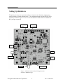
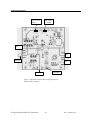
PLL Frequency
Synthesizer
Evaluation Kit
PE3293-EK
User’s Manual
6175 NANCY RIDGE DRIVE, SAN DIEGO, CA 92121
(858) 455-0660, FAX (858) 455-0770
http://www.peregrine-semi.com
Peregrine Semiconductor Corporation
1
Doc. 79/0003~03A
Table of Contents
FCC Labeling Requirement ........................................................... 3
Introduction .................................................................................... 4
Introduction ....................................................................................... 5
Getting Help ....................................................................................... 6
Internet ......................................................................................... 6
Customer Support .......................................................................... 6
Hardware Section........................................................................... 7
Evaluation Kit Contents ....................................................................... 8
Equipment Needed ............................................................................. 8
Setting Up Hardware ........................................................................... 9
Connecting the Power Supply ............................................................ 11
Parallel Port to 3-Wire Serial Interface Cable ....................................... 11
Software Section .......................................................................... 12
Software Introduction ....................................................................... 13
Description .................................................................................. 13
Screen Shots ............................................................................... 13
Installation ....................................................................................... 13
Operation ......................................................................................... 14
Overiew ...................................................................................... 14
Basic Operation ........................................................................... 14
1. Programming with the Frequency Input Loop Screens ............ 15
2. Programming with the Loop Block Diagrm Screens ............... 17
3. Programming with the Register Map Diagrm Screens ............. 19
4. Control Bits Window ........................................................... 20
5. Configuration Files .............................................................. 21
6. Printer Port Screen ............................................................. 21
Measuring lock time .......................................................................... 22
Test Results ..................................................................................... 23
Peregrine Semiconductor Corporation
2
Doc. 79/0003~03A
© Copyright 1999 Peregrine Semiconductor Corp. All rights reserved. Printed in the
United States of America. No part of this publication may be reproduced, photocopied,
stored in a retrieval system, or transmitted by electronic, mechanical or any other means
without prior written permission of Peregrine Semiconductor Corp.
Peregrine Semiconductor Corp., the Peregrine logotype, and UTSi are registered trademarks of Peregrine Semiconductor Corp. PE3293 is a trademark of Peregrine Semiconductor Corp.
Peregrine Semiconductor Corp. reserves the right to make improvments to the hardware,
firmware or software described in this manual at any time and without notice. While the
accompanying material has been carefully reviewed to insure the most accurate information possible, the data are not warranted for absolute accuracy or completeness and are
subject to change without notification.
Peregrine Semiconductor Corp. Life Support Policy
Peregrine Semiconductor Corp. products are not intended for use in life-critical situations,
or as critical components in life-support devices or systems.
Life-support devices or systems are defined as devices or systems that are intended for
surgical implant into the body, or that support or sustain life, and whose failure to
perform when used in accordance with the instructions provided by the manufacturer,
might result in injury to the user.
This device is intended for use only in a research and development environment. It has
not been tested for compliance with FCC regulations regarding interference with radio
frequency energy. It might cause harmful interference with radio communications. The
user assumes responsibliity for any interference caused by this device.
FCC Labeling Requirement
This device complies with Part 15 of the FCC Rules. Operation is subject to the following
two conditions: (1) this device may cause harmful interference, and (2) this device must
accept any interference received including interference that may cause undesired operation.
Peregrine Semiconductor Corporation
3
Doc. 79/0003~03A
Introduction
Peregrine Semiconductor Corporation
4
Doc. 79/0003~03A
Introduction
The PE3293-EK is a self contained dual PLL synthesizer on a 3.25” x 3.25” surface mount
circuit board. Externally it requires only power supplies, a reference frequency source and a
three-wire serial data programmer to make an operating dual frequency synthesizer. The board
is intended to illustrate the features of Peregrine’s fractional-N architecture and the benefits of
the UTSi process. The fractional-N PLL provides improved phase noise and low spurious
output levels. The UTSi process, with its insulating substrate, provides improved isolation to
limit crosstalk between the two PLL sections on the chip.The PE3293 minimizes current
consumption by allowing the user to choose the preferred trade off between speed and power.
The PE3293 has internal fractional spurious compensation. This compensation along with a
standard second order loop filter should limit the fractional spurs to -70 dBc or less. The
compensation requires no external components, tuning, or software commands. No special
circuit or layout features are needed on the demonstration board to fully utilize the fractional
spur compensation. The fractional spur compensation may cause stability problems if loop
bandwidths of more than 10% of the step size are used. The loop filter is a standard second
order passive filter, keeping in mind that N is calculated using the output frequency divided by
the comparison frequency, not the output frequency divided by the step size. Example: for fout
= 950 MHz, fcompare = 800 KHz, and fstep = 25 KHz, we have N = 950 / 0.8 = 1187.5. Pads
are provided on the board for installing additional components to make a 3rd order loop filter if
desired.
Special layout features are employed in the PE3293 demonstration board to maximize the
isolation between sections allowed by the fully insulating substrate of the PE3293. The power
supplies for the two VCOs are isolated and brought out to separate pins on the board. This
provides additional isolation and allows use of VCOs with power supply other than 3V.
The PE3293 board brings VDD1, the external bias for the PLL1 prescaler, and VDD2, the
external bias for the PLL2 prescaler out to separate jacks. This allows the user to set the speeds
and power usages of PLL1 and PLL2 independently. To minimize the number of power supply
needed for the evaluation board, the PLL1 and PLL2 external biases have been hard-wired to
the PLL main power supply (3V) through a voltage drop resistor (330 ohms for Vdd1 and 3.3
kohms for Vdd2). Note that only the PLL1 (RF) is populated, not the PLL2 (IF).
The outputs of the VCOs and the reference frequency input are via SMA jacks. The power
inputs and foLD output are configured for standard .100” center header pins. A test point is set
for the foLD output which can be connected to a SMA jack through a jumper.
Peregrine Semiconductor Corporation
5
Doc. 79/0003~03A
Getting Help
This User’s Manual covers all of the functions of the PE3293-EK program. The program uses well-established Windows user-interface conventions and is often self-explanatory. Still, we recommend that you read through this manual before using the program.
Internet
Software upgrades, frequently asked questions, and applications information can be
found on Peregrine’s website at http://www.peregrine-semi.com.
Customer Support
Our Applications Engineering staff will be happy to answer any questions you might have
about using the PE3293 or other Peregrine Semiconductor Corp. products. Contact us
at (858) 455-0660.
You may also contact us by fax or e-mail:
Fax:
(858) 455-0770
E-Mail:[email protected]
Peregrine Semiconductor Corporation
6
Doc. 79/0003~03A
Hardware
Section
Peregrine Semiconductor Corporation
7
Doc. 79/0003~03A
Evaluation Kit Contents
The Evaluation Kit includes all of the specific software and hardware required to evaluate the
PE3293. Included in the Evaluation Kit are:
1 PE3293 Evaluation Board
1 PE3293 1.8GHz/550MHz Dual Fractional-N PLL
1 CD with Application Software included
1 3-Wire Interface Cable with GND
2 Power Supply Cables
1 Set of Evaluation Kit Data Plots
Equipment Needed
Computer
•
•
•
•
•
Power Supply
•
•
Test Equipment
•
Intel CPU or equivalent (386 or later)
640 kB RAM
Microsoft Windows 95/98
Parallel port (LPT1)
Mouse (Microsoft or compatible)
3 VDC at 4 mA for PLL
4.1 VDC at 9 mA for VCO1 (Although VCO1 needs
only 3.3V, 4.1V is required to compensate the voltage drop
through a 100-ohm resistor).
Spectrum analyzer: HP 8561E or similar (phase noise and
spurious output measurement)
CAUTION: The PE3293-EK circuit contains components that might be
damaged by exposure to voltages in excess of the specified supply voltage
including voltages produced by electrostatic discharges. Handle the board in
accordance with procedures for handling static-sensitive components. Avoid
applying excessive voltages to the power supply terminals or signal inputs or
outputs.
Peregrine Semiconductor Corporation
8
Doc. 79/0003~03A
Setting Up Hardware
The primary test setup uses a spectrum analyzer to measure center frequency, output power,
spurious outputs, crosstalk and phase noise. The configuration used to test the PE3293-EK at
our facility is shown in Figures 1 and 2 for the evaluation kit with the PE3293 in TSSOP and
BCC package, respectively.
Vvco1 +4.1V
Input
PLL VDD
+3V Input
N/C
N/C
RF Out
N/C
REF In
Serial Input
Figure 1: PE3293 Evaluation Board Configuration for
PE3293 in TSSOP Package.
Peregrine Semiconductor Corporation
9
Doc. 79/0003~03A
Vvco1 +4.1V
Input
PLL VDD
+3V Input
N/C
N/C
RF Out
N/C
Serial Input
REF In
Figure 2: PE3293 Evaluation Board Configuration for
PE3293 in BCC Package.
Peregrine Semiconductor Corporation
10
Doc. 79/0003~03A
Connecting the Power Supply
Connect the PE3293-EK to suitable power supplies as shown in Fig. 1 or 2. The VDD to the
PE3293 is +3 volts. Although VCO1 needs only 3.3V, 4.1V is needed at VVCO1 terminal to compensate the voltage drop through a 100-ohm resistor. Because the PLL2 (IF) is not populated, no
power supply is required for the VVCO2 terminal. Connection can be made using dedicated wires
soldered into the supply holes or polarized pin plugs supplied with the evaluation kit.
PE3293 has to use the FlexiPower feature for VDD1 and VDD2. Vdd1 gets the required voltage
through a voltage drop resistor (330 ohms for Vdd1) connected to the PLL main power, 3V.
When using a 5 volt VCO, note that the maximum tuning voltage from the PE3293 will be 2.5
volts, and the tuning range of the VCO will be restricted on the high frequency end of the specified
frequency range of the VCO.
Parallel Port to 3-Wire Serial Interface Cable
Figure 3 shows the serial interface cable configuration. The PE3293 demonstration software outputs
a standard three-wire serial bus command from pins 2, 3, and 4 of the printer port of the computer.
The “Step” function carried on pin 5 of the printer port goes high with the LOAD ENABLE pulse
of the PLL1 main programming word. The software normally transmits all four programming
words, with the PLL1 main divider control word being the third word sent.
1
Clock
2
2
Data
3
3
LE
4
Ground
18
4
Cable Connector
Female 0.100” centers
Single row, 4 positions
Step
5
DB25 Male Connector
Figure 3. Serial Interface
Peregrine Semiconductor Corporation
11
Doc. 79/0003~03A
Software
Section
Peregrine Semiconductor Corporation
12
Doc. 79/0003~03A
Software Introduction
Description
The PE3293-EK software runs under Microsoft Windows 95/98. We use PE3292 software to
run PE3293, as well. The window screen or label may indicate PE3292, but procedure applies
to PE3293. It provides a convenient means of initializing and controlling the PE3293-EK
board. The user can enter frequencies directly, enter division values directly as decimal,
hexadecimal, or binary numbers, and set individual control register bits directly in a registermap window. The program calculates register values from user-specified frequencies and
performs range-checking on all values. The program communicates with the PE3293-EK
through a standard PC parallel port (LPT1, 2, or 3). The user can save the PE3293-EK control
settings as files for easy recall at any time.
Screen Shots
All screen images used in this manual are from Windows 95. The appearance of the windows
on your system might differ somewhat from the images in this manual, depending on the
version of Windows and type of display you are using.
Installation
1. Start Microsoft Windows. Insert the Peregrine CD into CDROM drive and
open CD directory. Click Sales, Products, and then PE3293 - 1.8GHz/550MHz
in the Phase Locked Loop list. Click Evaluation Board Software in the Evaluation Kit Documentation list. Choose Save this program to disk or Run this
program from its current location options. Either way, follow the instructions on
the screen.
2. Unzip the PE3293.exe file into an empty folder or directory.
3. Click the setup.exe file to start software installation procedure. Follow the
instructions on the screen.
Peregrine Semiconductor Corporation
13
Doc. 79/0003~03A
Operation
Overview
This section describes how to use all of the features of the PE3293-EK software to
control the PE3293-EK board. Since the PE3293-EK software uses a standard
three-wire interface, it can also be used to control customer-designed breadboards
or modified PE3293-EK boards. The PE3293-EK program performs range
checking on values entered by the user or calculated by the program, and warns the
user if certain limits are exceeded. The error messages are advisory; the program
will permit the user to enter values outside the normal operating range of the
PE3293. For example, an error message “fin exceeds operating limit”
appears in the screen of “Frequency Input Loop 1” if the fin is higher than
1100 MHz. This message can be ignored.
Basic Operation
The PE3293 is a dual PLL synthesizer IC. The 1.8 GHz PLL (PLL 1 or RF PLL)
and the 550 MHz PLL (PLL 2 or IF PLL) are programmed separately. Each PLL
requires two programming words. The programming words can be generated in one
of three ways. Three types of screen can be used to set the frequency of the PLLs.
These are the Frequency Input Loop screens, which accepts frequency values,
the Loop Block Diagram screens, which accept numbers to directly program the
count registers, and the Register Map screen, which allows the binary control
words to be set directly into the programming word registers.
If the Frequency Input Loop screens or the Loop Block Diagram screens are
used to program the PLL then a third screen, the Control Bits screen must be used
to set the output state of the PLL and the function of the foLD pin. For the
PE3292 the control bits screen also sets the FlexiPower function of the prescalers.
If the Register Map screen is used to set the PLLs the control bits can be set
directly in the Register Map screen.
The different screens can be accessed with the View menu from any window. The
control bits screen can be accessed from the options menu.
Peregrine Semiconductor Corporation
14
Doc. 79/0003~03A
1. Programming with the Frequency Input Loop Screens
The reference frequency, output frequency, step size, step number and comparison frequency can
be specified on the Frequency Input Loop screens. Figure 4 shows one screen of the “Frequency
Input Loop 1”. This screen can be activated by clicking the View on the main menu and select
Frequency Input Loop 1.
Figure 4. Frequency Input Loop 1 Screen.
Note: When programming the PE3293 to a frequency higher than 1.1 GHz, an error message will
appear stating “fin exceeds operating limit.” This error is derived from a known software issue and
should be ignored.
Note that the Frequency Input Loop 1 and the Frequency Input Loop 2 screens are identical in
appearance and function except that the prescaler for Loop 1 is a divide by 32 or 33, and the
prescaler for Loop 2 is a divide by 16 or 17.
The Frequency Input screens are the basic method for programming the PLLs. These screens
allow you to enter the reference frequency (fr), starting frequency, step size, step number,
maximum fractionality, and comparison frequency (fc) or reference divider ratio (R) value. From
these entered values, the software will calculate the values for the boxes in green. When fc is
changed, the software will recalculate the value of R, and vice versa.
Peregrine Semiconductor Corporation
15
Doc. 79/0003~03A
When both Frequency Input Loop screens have been programmed to the desired fin. Calc., the
settings from both screens can be sent to the output port by clicking on Send at the bottom of
either Frequency Input Loop screen or by typing Alt S.
There are a number of conditions for correct operation of the PE3293.
1. fr must be an integer multiple of fc. (i.e. R must be an integer)
2. fr must be an integer multiple of Step Size
3. Step Size must be equal to fc divided by 1, 2, 4, 8, 16, or 32.
4. Step Number must produce a calculated value for F which is compatible with Max.
fractionality.
• F = 0 for any Max. fractionality.
• F = any value for Max. fractionality of 32.
• F = even values for Max. fractionality of 16.
• F = multiples of 4 for Max. fractionality of 8.
• F = multiples of 8 for Max. fractionality of 4.
• F = multiples of 16 for Max. fractionality of 2.
• F = 0 for Max. fractionality of 1.
5. The desired output frequency must be achievable.
A. The desired output frequency (fin. Spec.) will be calculated as:
1) (Starting freq.) + (Step Size X Step Number).
B. The closest achievable frequency (fin. Calc.) will be calculated as:
1) (32 x M1 x fc1) + (A1 x fc1) + (F1/32 x fc1) for the Loop 1
screen
2) (16 x M2 x fc2) + (A2 x fc2) + (F2/32 x fc2) for the Loop 2
screen
C. fin. Spec. and fin. Calc. must match or an error message will be
displayed.
Failure to meet any of these conditions will result in an error message in the dialog box under the
Inputs window.
Input the numbers in the clear boxes by clicking on the box and typing the values in. Enter the
values by moving to another box, clicking outside the box, clicking Send or hitting the enter key.
For the Step Number, you may type the value into the box or use the up and down buttons to
increment or decrement the value by 1. The Max Fractionality is input by clicking on the box to
show its pull down list and then clicking on the desired Max Fractionality on the list.
The user must provide fr. This is the reference frequency available from your reference source.
The external reference is supplied to the input of both reference counters in the PE3293. The user
must then specify either fc or R. The program will calculate the remaining term. If you change fc
or R, the program will recalculate the other term to fit. If you specify a value for fc that cannot
be generated by dividing fr by an integer between 3 and 511, there will be an error message, “fr
is not an integer multiple of fc.”
Peregrine Semiconductor Corporation
16
Doc. 79/0003~03A
The Starting freq, Step Size, and Step Number are provided by the user. The program will
calculate fin Spec. = Starting freq + (Step Size X Step Number). The program will then generate
fin Calc. as the closest value that can be achieved using integer values for M, A, and F. If fin
Spec. cannot be achieved using integer values of M, A, and F, there will be an error message,
“Cannot achieve specified fin.”
Note: When programming the PE3293 to a frequency above 1.1 GHz, an error message will
appear stating “fin exceeds operating limit.” This error is derived from a known software issue
and should be ignored.
In general, the step size should be chosen as fc/Max fractionality and the Starting frequency
should be an integer multiple of the Step Size. Failure to do so will usually lead to numerous nonMax fractionality is set by choosing 1, 2, 4, 8, 16, or 32 from the pull down list for Max
Fractionality on the Frequency Input Loop screen. If the calculated value for F is not zero or a
multiple of 32/ Max fractionality, the error message “Max fractionality exceeded” will appear.
The values of M, A, and F cannot be entered directly in the Frequency Input Loop 1 screen. If
you wish to enter these values directly, see the “Programming With the Loop Block Diagram
Screen” below.
2. Programming with the Loop Block Diagram Screens
The count numbers for the A, F, M, and R counters can be input into the Block Diagram screen
as shown in Figure 5 as Loop 1 Block Diagram.
Note that the Loop 1 Block Diagram and the Loop 2 Block Diagram screens are identical in
appearance and function except that the prescaler block for Loop 1 shows a divide by 32 or 33 ,
and the prescaler block shown for Loop 2 is a divide by 16 or 17.
The Loop Block Diagram screens allow the user to input the values for A, F, M, and R (the
numbers shown in green) directly to the registers. The values for fin. Calc. and fc (shown in
black) can be changed only by changing A, F, M, or R, or by going to the Frequency Input
screen. If the resulting values of fin. Calc. or fc result in an error condition , the number will
display in red in the Loop Block Diagram screen. If the resulting value of fin. Calc. does not
agree with the fin. Spec. from the Frequency Input screen, the number will appear in red in the
When a Loop Block Diagram screen is open, the Number System window is active on the
main menu bar. This allows input and viewing of A, F, M, and R in decimal, hex, or binary by
clicking on Number System to pull down the menu and choosing the desired numbering system.
The default setting will be in decimal.
Peregrine Semiconductor Corporation
17
Doc. 79/0003~03A
Figure 5. PE3293 Loop 1 Block Diagram.
The Loop Block Diagram screen is useful when you have already calculated the register values
or when you wish to view the register values calculated by the program in a more intuitive
To program Loop 1, go to View on the main menu and select Loop 1 Block Diagram (Fig. 5). In
this screen you can specify the count value of the A, F, M, and R counter registers for Loop 1.
The A, F, M, and R values can be entered and displayed in decimal, hexadecimal, or binary
format.
The value of fr must be specified in the Frequency Input Loop 1 screen. The values of A, F,
M, and R from the Loop 1 Block Diagram will be transfered to the Frequency Input Loop 1
screen and used to calculte fin Calc. If the choices of A, F, M, or R entered in the Loop 1
Block Diagram cause an error message in the the Frequency Input Loop 1 screen, the value for
fin 1 displayed in the Loop 1 Block Diagram will appear in red.
Note: If R1 is changed in the Loop 1 Block Diagram, the comparison frequency (output of the
R1counter) in the Loop 1 Block Diagram screen will change to the new calculated value.
Peregrine Semiconductor Corporation
18
Doc. 79/0003~03A
3. Programming with the Register Map Screens
The Register Map screen as shown in Figure 6 allows you to set the state of any accessible bit in
the registers of the PE3293. Bits that you can set are green. Fixed or reserved bits are gray. To
access the Register Map screen, go to View on the main menu and select Register Map.
Figure 6. PE3293 Register Map Screen.
To program in the Register Map screen, place the cursor on the bit that you want to change and
press the 0 or 1 keys to change the value. In this view, the program recognizes changes immediately. It is not necessary to move the cursor to enter the new value. The control bits for the
PE3293 can be entered directly in the Register Map view to turn the individual PLLs on or off,
control the foLD output and set the charge pump Output Options.
Once the desired bits are entered click on Send to program the PE3293. You can use this feature
with the Send Continuous mode to change individual bits while automatically updating the
PE3293.
Peregrine Semiconductor Corporation
19
Doc. 79/0003~03A
4. Control Bits Window
Except in the Register Map mode,when the PLL frequency is set using either the Frequency
Input Loop screens or the Loop Block Diagram screens, the settings for the Loop Output
Options, the Prescaler FlexiPower Setting and foLD Control must be set using the Control
Bits window as shown in Figure 7.
To access the Control Bits window, go to Options in the main menu and click on Control Bits
to display
the Control Bits window. Click on any foLD Control button to choose that output function for
the foLD pin. The Loop Output Options are toggled by clicking on the function buttons. The
On button toggles the entire PLL on or off. The Invert button sets the charge pump of that loop
to invert the current sink and source relationship. The Hi-Z button turns the charge pump for that
loop off, creating a high impedance at the charge pump output.
If using the PE3293, click on one of the Prescaler FlexiPower Setting buttons to control the
prescaler function.
After the foLD Control, both Loop Output Options, and the Prescaler FlexiPower Setting (if
using the PE3293) are set to the desired states, click on Ok to transfer the new states to the
control word registers and close the window.
Figure 7. Control Bits Window. Note that none of the Loop 2 Output
Options was selected because the Loop 2 was not populated.
20
Peregrine Semiconductor Corporation
20
Doc. 79/0003~03A
5. Configuration Files
All of the register values and control states can be saved as files. Later, you can reload a saved
configuration to restore the PE3293-EK to a particular state without having to re-enter all of the
values.
Saving Configurations
From the File menu, choose Save Settings As.
In the Save As dialog box, select a directory and enter a file name, then click OK.
Loading Configurations
From the File menu, choose Load Setings.
In the Open dialog box, select a directory and a file, then click OK.
6. Printer Port Screen
The default output of the PE3293-EK software is through the LPT1 printer port as shown in
Figure 8. If you wish to use a different port to control the PE3293, go to Options, click on
Parallel Port and click on the button for the port you wish to use. Click on OK to set the output
to the selected port. The data will now be sent out through the new selected port when you click
on Send.
Figure 8. Printer Port Screen.
Peregrine Semiconductor Corporation
21
Doc. 79/0003~03A
Measuring lock time
The PE3293 software has two modes for use in measuring the lock time of PLL1.
The Toggle mode allows switching repeatedly back and forth between two chosen
frequencies. This is well suited to checking the coarse frequency acquisition by
monitoring the tuning voltage of a synthesizer using an oscilloscope, or when using
a mixer and oscilloscope to measure the phase difference between a PLL already
locked on frequency, and the experimental PLL. The standard programming mode
is more useful when measuring the lock up time as a one-shot event using a Modulation Domain Analyzer or similar instrument.
To use Toggle Mode click on Options to pull down the menu and then click on
Toggle Mode. Click on Options again. You will now see that the Repetition Rate
and Toggle Setting options are available.
Click on Repetition Rate. The Repetition Rate window will ask you to set a
number for the delay time. The actual time period represented by this number will
be machine dependent. You will have to experiment to determine the delay number
needed to give the desired time between stepping events for your computer.
Click on Toggle Setting. The Toggle Setting window will ask you to chose the
number of step sizes you wish to jump at each toggle event. The output frequency
will toggle between the specified frequency (fin Spec.) in the Frequency Input
Loop 1 screen and a frequency that is the set number of steps above or below the
starting frequency. A step is defined by the Step Size entry of the Inputs box of the
Frequency Input Loop 1 view. As an example if we set the Staring Frequency to
1730.4 MHz, the Step Size to 12.5 KHz and the Step Number to 1 we will get an
fin Spec. of 1730.4125 MHz. A Toggle Setting of 5 steps will then cause the
frequency to toggle between 1730.4125 MHz and 1730.475 MHz. A Toggle
Setting of -5 steps will cause the frequency to toggle between 1730.4125 MHz
and 1730.35 MHz.
When the Toggle Mode is used, the software sends only the programming word for
the PLL1 main divider. The rising edge of the Load Enable pulse can be used as a
start signal for measuring lock up time. The Load Enable pulse is present on pin 4
Peregrine Semiconductor Corporation
22
Doc. 79/0003~03A
of the DB25 connector, pin 3 of J3, and pin 13 of the IC. When done as a one-shot event
there is no way to distinguish between jumping to the toggle frequency and jumping back to
the specified frequency.
To use the standard programming mode to measure lock time as a single event with a
Modulation Domain Analyzer, an output for use as the trigger has been provided on pin 5
of the DB25 connector. When the standard programming mode is used the software always
sends all four programming words. The word for the PLL1 main divider is the third word
in the series. This makes it difficult to use the Load Enable pulse as the trigger for measuring lock time. The output provided on pin 5 of the DB25 connector gives a pulse which is
synchronous with the PLL1 main divider Load Enable pulse. This output is labeled
“Step”(see Fig. 3, Page 11). This signal is not available on the PE3293 board. It must be
taken from the DB25 connector.
Test Results
Three test plots are normally enclosed. Two of them are the phase noise plots with a 10 MHz
square wave or a 19.2 MHz sine wave as the reference. The third plot is a linear plot to show the
step size spur.
The test data are measured with the following parameters for PLL1 Frequency Input Loop 1:
fr (Reference freq.) (MHz):
Starting frequency (MHz):
Step size (KHz):
Step number:
Max fractionality:
fc (comparison frequency) (KHz)
Peregrine Semiconductor Corporation
10
1750.2125
12.5
0
16
160
23
19.2
1750.09
10
0
16
160
Doc. 79/0003~03A