1
PC104-30F and PC104-30G Series User’s Manual
Chapter 5: Register Structure
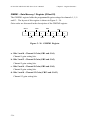
c. Bit 2 - DMA Enable
DMA operations are controlled by the combination of bit 2, and the DMA
mode bit in the ADMDE register. This interaction of the DMA enable bit and
the DMA mode bit is explained in the description of the ADMDE register.
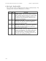
d. Bit 1- Strobe Select (STBC)
This bit controls the source of A/D strobes to the A/D converter. If it is set,
then software strobes are used. Software strobes are generated by toggling
the SSTB bit (bit 0). If the STBC bit is cleared, then A/D clock pulses are
used to start A/D conversion cycles. A/D clock pulses may be generated
from the A/D clock prescaler/divider combination, or from an external source.
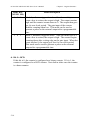
e. Bit 0 - Strobe (SSTB)
Bit 0 of the ADCCR is the software strobe bit. If the STBC bit is set, then a
software strobe is generated by taking the strobe bit high, then low. If the
STBC bit is low, then the SSTB bit is ignored.
WHENEVER YOU CHANGE THE
STATE OF THE STBC BIT, THE
SSTB BIT MUST BE 0 (CLEARED).
IF THE SSTB BIT IS NOT CLEAR,
SPURIOUS A/D CONVERSION
CYCLES MAY BE GENERATED.
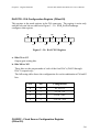
ADMDE - A/D Mode Register (Offset 3)
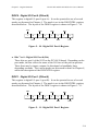
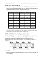
The ADMDE register contains A/D mode selection bits, the error reset control
bit and the DMA mode control bit. The bit functions of the ADMDE register are
shown in Figure 5 - 5.
If your application requires 100% compatibility with older PC26, PC104-30 or
PC39 boards, you should write the value 92 (hex) to this register.
5-8