1
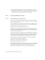
U2P™
UPA to PCI Interface User’s Manual
A Sun Microsystems, Inc. Business
2550 Garcia Avenue
Mountain View, CA 94043 USA
1-800-681-8845
www.sun.com/sparc
Part No.: 802-7835-01
May 1997
Copyright © 1997 Sun Microsystems, Inc. All Rights Reserved.
THE INFORMATION CONTAINED IN THIS DOCUMENT IS PROVIDED “AS IS”
WITHOUT ANY EXPRESS REPRESENTATIONS OR WARRANTIES. IN ADDITION, SUN
MICROSYSTEMS, INC. DISCLAIMS ALL IMPLIED REPRESENTATIONS AND
WARRANTIES, INCLUDING ANY WARRANTY OF MERCHANTABILITY, FITNESS FOR A
PARTICULAR PURPOSE, OR NON-INFRINGEMENT OF THIRD PARTY INTELLECTUAL
PROPERTY RIGHTS.
This document contains proprietary information of Sun Microsystems, Inc. or under license
from third parties. No part of this document may be reproduced in any form or by any means
or transferred to any third party without the prior written consent of Sun Microsystems, Inc.
Sun, Sun Microsystems, and the Sun logo are trademarks or registered trademarks of Sun
Microsystems, Inc. in the United States and other countries. All SPARC trademarks are used
under license and are trademarks or registered trademarks of SPARC International, Inc. in the
United States and other countries. Products bearing SPARC trademarks are based upon an
architecture developed by Sun Microsystems, Inc.
The information contained in this document is not designed or intended for use in on-line
control of aircraft, air traffic, aircraft navigation or aircraft communications; or in the design,
construction, operation or maintenance of any nuclear facility. Sun disclaims any express or
implied warranty of fitness for such uses.
Printed in the United States of America.
Contents
1.
Overview 1-1
Introduction 1-1
Product Summary 1-2
Technology 1-2
Package 1-2
Design Size 1-2
Custom Cells 1-2
Maximum Frequency of Operation 1-3
Minimum Frequency of Operation 1-3
Power Consumption 1-3
Performance 1-4
Typical System Partition 1-5
U2P External Interfaces 1-5
U2P Block Diagram 1-7
U2P Block Overviews 1-8
UPA Interface blocks 1-8
PCI Interface blocks 1-8
Interrupt block 1-9
Internal Control 1-9
Clock Ratios 1-10
Miscellaneous 1-10
PCI Address Map Overview 1-10
Contents
iii
2.
U2P Pin Descriptions 2-1
UPA Interface Signals 2-1
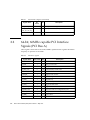
64-bit, 66MHz capable PCI Interface Signals (PCI Bus A) 2-2
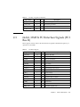
64-bit, 33MHz PCI Interface Signals (PCI Bus B) 2-3
Miscellaneous Interfaces 2-4
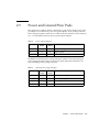
Power and Ground Pins/Pads 2-5
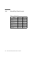
Total Pin/Pad Count 2-6
3.
U2P Functional Description 3-1
Functional Overview 3-1
Top-Level Architectural Philosophy 3-1
Block Overviews 3-4
PIO Decoder 3-4
DMA Control 3-4
Bus Control 3-5
UPA Master / Slave 3-5
UPA Reply 3-6
ECC Generate / Check 3-6
DMA Merge Buffer 3-7
PCI Bus Module (PBM) 3-7
IOMMU 3-10
Streaming Cache 3-10
MDU 3-11
Timer / Counters 3-12
Reset 3-12
Testability 3-13
4.
DMA/PIO Transactions Flow 4-1
Block Diagram 4-2
DMA Transaction Flow 4-5
DMA Write Transactions 4-6
64 and 16 Byte DMA Writes to IO Space 4-6
64 Byte DMA Write to Memory 4-8
Less than 64 Byte DMA Write to Memory 4-10
DMA Read Transactions 4-13
iv
UPA to PCI Interface (U2P) User’s Manual • May 1997
PIO Transaction Flow 4-14
PIO Write 4-15
PIO Read 4-17
5.
IOMMU 5-1
Block Diagram 5-2
TLB Entry Format 5-2
TLB CAM Tag 5-3
TLB RAM Data 5-3
DVMA Operation Modes 5-4
Translation Mode 5-4
Bypass Mode 5-5
Pass-through Mode 5-6
Translation Storage Buffer 5-6
Translation Table Entry 5-7
TSB Lookup 5-7
PIO Operations 5-9
Translation Errors 5-9
IOMMU Demap 5-10
TLB Initialization and Diagnostics 5-10
6.
PCI Bus Interface 6-1
Introduction 6-1
Supported PCI features: 6-1
Unsupported PCI features: 6-2
PCI Bus Operations 6-2
Bus Master Operation (PIO) 6-2
Target Operation (DMA) 6-4
Transaction Termination Behavior 6-5
Retries 6-5
Disconnects 6-5
Master-aborts 6-5
Target-aborts 6-6
Addressing Modes 6-7
Contents
v
Configuration Cycles 6-7
Special Cycles 6-7
Exclusive Access 6-8
Fast Back-to-Back Cycles 6-8
Functional Topics 6-9
PCI Arbiter 6-9
Arbitration Scheme 6-9
Bus Parking 6-9
Endianess 6-10
PCI Commands 6-10
Diagnostic Modes 6-11
Clocks 6-11
Reset 6-11
7.
Streaming Cache Operation 7-1
Overview 7-1
Streaming Cache Conceptual Overview 7-2
STC Subsections 7-2
Streaming Cache Functional Description 7-3
Streaming Writes 7-3
Byte Holes and Zero Byte Writes 7-4
Streaming Reads 7-4
Entry Flushing 7-5
Streaming Cache Programming Model 7-6
Performance Issues 7-6
Memory Coherency Maintenance 7-7
Error Recovery 7-8
8.
Mondo Dispatch Unit 8-1
Overview 8-1
Mondo Dispatch Overview 8-1
Mondo Dispatch Block Diagram 8-3
Mondo Unit Functional Description 8-3
Mondo Vectors 8-4
vi
UPA to PCI Interface (U2P) User’s Manual • May 1997
Overview of an Interrupt 8-4
Interrupt Number Register 8-5
Interrupt Types 8-6
Internal/External 8-6
Level/Pulse 8-7
Priority 8-8
Synchronization with DMA writes 8-9
Interrupt Table 8-9
Processing an Interrupt 8-11
Interrupt Receiver 8-12
Interrupt Decoder 8-12
Interrupt Arbiter 8-12
Interrupt Dispatcher 8-12
9.
U2P Timer/Counter 9-1
Overview 9-1
Timer Functional Description 9-2
10.
Little-endian support 10-1
Big- and Little-endian regions 10-1
Address Space 10-1
Internal blocks 10-2
Byte Twisting 10-2
Specific Cases 10-4
PIOs 10-4
DMA 10-5
11.
Error Handling 11-1
Overview 11-1
Fatal Hardware Errors 11-1
UPA Address Parity Error 11-1
Non-fatal Hardware Error 11-2
UPA Datapath Uncorrectable Error 11-2
UPA Timeout 11-3
UPA Read Error 11-3
Contents
vii
PCI Data Parity Error 11-3
PCI Target-Abort 11-4
PCI Timeout 11-4
DVMA ECC Error 11-5
IOMMU Translation Error 11-5
PCI Address Parity Error 11-5
PCI System Error 11-6
Summary of Error Reporting 11-6
Unreported Errors 11-9
12.
JTAG 12-1
Introduction 12-1
TAP Controller 12-2
Synchronous FSM and Decode 12-5
Instruction Register 12-5
Instruction Decode Logic 12-6
Bypass Register 12-6
Internal Register Clocking Logic 12-7
JTAG ID Register 12-7
Boundary Scan Control Logic 12-7
BIST Control Logic 12-7
Clock Control Registers 12-8
Clock Stop Logic 12-8
TDO MUX logic 12-8
Scan Chains 12-9
Boundary Chain 12-9
The Internal Scan Chain 12-9
ATPG Chain 12-10
Special JTAG Instructions 12-10
INTEST 12-10
The ATPG Instruction 12-10
The RUNBIST Instruction 12-11
Test Coverage Information 12-11
ATPG 12-11
BIST 12-12
viii
UPA to PCI Interface (U2P) User’s Manual • May 1997
13.
Programmer’s Model 13-1
Internal Registers 13-1
U2P Control/Status Register 13-2
UPA Registers 13-4
UPA Port ID Register 13-4
UPA Configuration Register 13-5
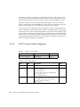
ECC Registers 13-6
ECC Control Register 13-6
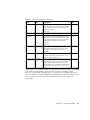
Uncorrectable Error Asynchronous Fault Status/Address Register 13-7
Correctable Error Asynchronous Fault Status/Address Register 13-9
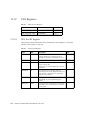
DMA Scoreboard Diagnostic Support 13-10
PCI Bus Module 13-12
PCI Control/Status Register 13-13
PCI Asynchronous Fault Status/Address Registers 13-14
PCI Diagnostic Register 13-17
PBM Configuration Space 13-18
Vendor ID 13-20
Device ID 13-20
Command Register 13-21
Status Register 13-22
Revision ID Register 13-22
Programming I/F Code Register 13-23
Sub-class Code Register 13-23
Base Class Code Register 13-23
Latency Timer Register 13-23
Header Type Register 13-24
Bus Number 13-24
Subordinate Bus Number 13-24
Unimplemented Registers 13-24
IOMMU Registers 13-25
IOMMU Control Register 13-25
TSB Base Address Register 13-28
Flush Address Register 13-29
TLB TAG Diagnostics Access 13-29
Contents
ix
TLB Data RAM Diagnostic Access 13-30
LRU Queue Diagnostic Access 13-31
Virtual Address Diagnostic Register 13-31
TLB Tag Compare Diagnostic Access 13-32
Streaming Buffer Registers 13-33
Streaming Buffer Control Register 13-34
Streaming Buffer Page Invalidate/Flush Register 13-35
Streaming Buffer Flush Synchronization Register 13-35
Streaming Buffer Page Tag Diagnostic Access 13-36
Streaming Buffer Line Tag Diagnostic Access 13-36
Streaming Buffer Data RAM Diagnostic Access 13-37
Streaming Buffer Error Status Diagnostic Access 13-37
Interrupts 13-38
Partial Interrupt Mapping Registers 13-40
Full Interrupt Mapping Registers 13-42
Clear Interrupt Registers 13-43
Interrupt State Diagnostic Registers 13-45
Interrupt Retry Timer Register 13-48
Counter/Timer Registers 13-49
Count Registers 13-49
Limit Registers 13-50
Performance Monitor Registers 13-50
Performance Monitor Control Register 13-51
Performance Counter Register 13-53
PCI Address Spaces 13-53
UPA to PCI 13-53
PCI Configuration Space 13-54
Special Cycles 13-56
PCI I/O Space 13-56
PCI Memory Space 13-56
PCI to UPA 13-57
PCI Configuration Space 13-57
PCI I/O Space 13-57
PCI Memory Space 13-57
Address Map Summary 13-59
x
UPA to PCI Interface (U2P) User’s Manual • May 1997
Figures
Typical PCI UltraSPARC System Block Diagram 1-5
U2P External Interfaces 1-6
U2P Conceptual Block Diagram 1-7
U2P PIO and DVMA address spaces 1-11
PIO Data & Address Paths 3-2
DMA Data & Address Paths 3-3
Top level block diagram for DMA and PIO transactions flow/control 4-2
DMA Write to IO space 4-6
64 Bytes DMA Writes to Memory 4-8
Less than 64 Bytes DMA Writes to Memory 4-10
DMA read request to memory or IO space 4-13
PIO Write Transaction Flow 4-15
PIO Read Transaction Flow 4-17
IOMMU top level block diagram 5-2
Virtual to physical address translation for 8K page size 5-5
Virtual to physical address translation for 64K page size 5-5
Physical address formation in bypass mode (8K and 64K) 5-5
Figures
xi
Physical address formation in pass-through mode (8k and 64K) 5-6
Computation of TTE Entry Address 5-8
Basic PCI Read Transaction 6-3
Basic PCI Write Transaction 6-3
Retry Cycle 6-5
Disconnect Cycle 6-6
Master-abort Cycle 6-6
Target-abort Cycle 6-7
Special Cycle 6-8
Fast Back-to-Back Cycles 6-9
Mondo Dispatch Unit in U2P 8-2
Mondo Dispatch Overview Block Diagram 8-3
Mondo Vector Format on UPA Data Bus 8-4
Full INR Contents 8-5
Partial INR Contents 8-6
Level Interrupt States 8-8
U2P Byte Twisting 10-3
TAP Controller Block Diagram 12-2
U2P Data registers 12-3
JTAG control signals during ATPG instruction 12-11
Legal DVMA address configurations 13-27
U2P Interrupt Format 13-38
Type 0 Configuration Address Mapping 13-55
Type 1 Configuration Address Mapping 13-55
xii
UPA to PCI Interface (U2P) User’s Manual • May 1997
Tables
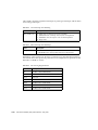
U2P Absolute Best Case Performance 1-4
UPA Interface Signals 2-1
PCI Bus A signals 2-2
PCI Bus B Signals 2-3
Miscellaneous Signals 2-4
Power and ground pins 2-5
Special power and ground pins 2-5
Total Pin Count 2-6
Type of P_REQ and S_REPLY used for DMA write to IO space 4-7
Type of S_REPLY’s U2P receives 4-7
Type of P_REQ and S_REPLY used for 64 byte DMA writes to memory 4-9
Type of P_REQ and S_REPLY used for less than 64 byte DMA writes 4-11
Type of P_REQ and S_REPLY used for DMA reads 4-14
Type of write P_REQ’s U2P receives and type of P_REPLY it generates 4-16
Type of P_REPLY’s generated by U2P 4-16
Type of read P_REQ’s U2P receives and type of P_REPLY it generates 4-18
Description of TLB Tag Fields 5-3
Tables
xiii
TLB Data Format 5-3
PCI DVMA Modes of Operation 5-4
TTE Data Format 5-7
Offset to TSB Table 5-8
PCI Command Generation and Response 6-10
Level Interrupt States 8-7
Interrupt Receiver State Register 8-8
Summary of Interrupts 8-10
Summary of Fatal Error Reporting 11-6
Summary of Non-Fatal Error Reporting 11-7
Description of signals in JTAG macro 12-3
Components of the U2P TAP controller 12-4
Instructions supported by U2P JTAG controller 12-5
U2P scan chains 12-9
BIST register files 12-12
Non-BIST register files 12-13
Offset of Control Register 13-2
U2P Control Register 13-2
Offset of UPA Registers 13-4
UPA Port ID Register 13-4
UPA Configuration Register 13-5
Offset of ECC Registers 13-6
ECC Control Register 13-6
ECC Error Reporting 13-7
UE AFSR 13-8
xiv
UPA to PCI Interface (U2P) User’s Manual • May 1997
UE AFAR 13-8
CE AFSR 13-9
CE AFAR 13-10
Offset of DMA Scoreboard Diagnostic Access 13-10
DMA Scoreboard Diagnostic Access 13-11
Offset of PBM Registers 13-12
PCI Control and Status Register 13-13
PCI AFSR 13-15
PCI AFAR 13-16
PCI Diagnostic Register 13-17
Default offset of PCI Bridge Configuration Spaces 13-18
Configuration Space Header Summary 13-19
Command Register 13-21
Status Register 13-22
Latency Timer Register 13-23
Header Type Register 13-24
Offset of IOMMU Registers 13-25
IOMMU Control Register 13-25
Address space size and base address determination 13-26
TSB Base Address Register 13-28
Flush Address Register 13-29
TLB Tag Diagnostics Access 13-29
TLB Data RAM Diagnostics Access 13-30
LRU Entry Diagnostics Access 13-31
Virtual Address Diagnostic Register 13-31
TLB Tag Comparator Diagnostics Access 13-32
Offset of Streaming Buffer Registers 13-33
Streaming Buffer General Control Register (2 copies) 13-34
Streaming Buffer Page Invalidate/Flush Register (2 copies) 13-35
Tables
xv
Streaming Buffer Flush Synchronization Register (2 copies) 13-35
Streaming Buffer Page Tag Format 13-36
Streaming Buffer Line Tag Format 13-36
Streaming Buffer Data RAM Content Format 13-37
Streaming Buffer Data RAM Error Format 13-37
Interrupt Number Offset Assignments 13-39
Offset of Partial Interrupt Mapping Registers 13-40
Format of Partial Interrupt Mapping Registers 13-42
Offset of Full Interrupt Mapping Registers 13-42
Format of Full Interrupt Mapping Registers 13-43
Offset of Clear Interrupt Pseudo Registers 13-43
Clear Interrupt Register 13-45
Offset of Interrupt State Diagnostic Registers 13-45
Level Interrupt State Meaning 13-46
Pulse Interrupt State Meanings 13-46
PCI Int Diag Reg Definition 13-46
OBIO and Misc Int Diag Reg Definition 13-47
Offset of Interrupt Retry Timer Registers 13-48
Interrupt Retry Timer Register 13-48
Offset of Counter/Timer Registers 13-49
Count Register 13-49
Limit Register 13-50
Offset of Performance Monitor Registers 13-50
Performance Monitor Control Register 13-51
Performance Counter Event Sources 13-51
Performance Counter Register 13-53
Offsets for access from UPA space to PCI space 13-53
PCI DVMA Modes of Operation 13-58
Address Map Summary 13-59
xvi
UPA to PCI Interface (U2P) User’s Manual • May 1997
CHAPTER
1
Overview
1.1
Introduction
The U2P chip is the primary connection on an UltraSPARC CPU board between the
UPA System Bus (including UltraSPARC Processors and Memory) and a PCI based
I/O Subsystem. U2P features include:
■
Full master and slave port connection to the high-speed UltraSPARC UPA
Interconnect. The UPA is a split address/data packet-switched bus which has a
potential data throughput rate of over 1 Gbyte/sec. UPA data is ECC protected.
■
Two physically separate PCI bus segments, with full master and slave support.
PCI Bus A has the following features:
■
5 volt or 3.3 volt signalling.
■
64-bit data bus.
■
Compatible with the PCI Rev 2.1 Specification.
■
Compatible with the PCI 66MHz extensions.
■
Support for up to four master devices (at 33MHz only).
PCI Bus B has the following features:
■
■
5 volt signalling.
■
64-bit data bus.
■
Compatible with the PCI Rev 2.1 Specification.
■
Support for up to six master devices.
Two separate 16-entry streaming caches, one for each bus segment, for
accelerating some kinds of PCI DVMA activity. Single IOMMU with 16-entry TLB
for mapping DVMA addresses for both busses.
1-1
■
A “Mondo-Vector” Dispatch Unit, or MDU, for delivering Interrupt requests to
UltraSparc CPU modules, including support for PCI interrupts from up to six
total slots, as well as interrupts from on board IO devices.
1.2
Product Summary
1.2.1
Technology
■
1.2.2
1.2.3
1.2.4
0.35 micron, 3 level metal, 3.3 volt optimized CMOS standard cell library from
Lucent Technologies (formerly AT&T).
Package
■
The U2P die has 352 signal pads (including specialty power/grounds) and 104
VSS/VDD pads for a total pad count of 456.
■
The U2P package is a 456 ball PBGA, with 352 signal balls and 104 VSS/VDD
balls.
Design Size
■
170K gates.
■
29K bits RAM.
■
Die size = 404.7 x 435.4 mils (10280 x 11060 microns)
Custom Cells
The following non-standard cells are used in the U2P chip design:
1-2
■
5V tolerant PCI pads.
■
66MHz capable PCI pads.
■
UPA pads (with and without holding amps).
■
PLL and PECL receiver for UPA clock.
■
PLL for main clock.
UPA to PCI Interface (U2P) User’s Manual • May 1997
1.2.5
1.2.6
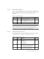
Maximum Frequency of Operation
■
UPA operation (UPACLK) up to 100 MHz (10 ns).
■
Main internal clock (PSYCLK) up to 66.7 MHz (15 ns).
■
PCI bus A clocks at 1x or 0.5x internal clock (synchronous).
■
PCI bus B clocks at 0.5x internal clock (synchronous).
Minimum Frequency of Operation
At times it is desirable to run the clocks at less than their intended frequencies.
For reliable operation, certain ratios between UPACLK and PSYCLK must be
maintained.
1.2.7
■
UPACLK > 0.9 * PSYCLK if Mode bit = 1 (Control/Status Reg bit 0).
■
PSYCLK > 0.41 UPACLK
Power Consumption
■
Maximum power consumption: 3 Watts.
Chapter 1
Overview
1-3
1.3
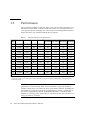
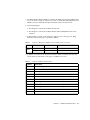
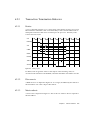
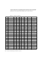
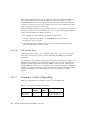
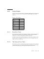
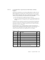
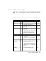
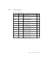
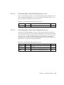
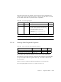
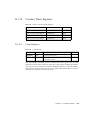
Performance
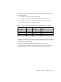
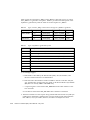
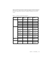
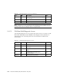
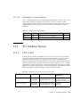
The performance numbers in the table below were extracted from simulations. For
PIO and Consistent DMA, 16 back-to-back transactions were simulated, the first 4
were ignored, and the remaining ones were timed. For Streaming DMA, 64 back-toback transactions were simulated and the first 16 ignored.
Table 1-1
Xfer
Size
U2P Absolute Best Case Performance
Bus speed Bus Width
PIO Wr
PIO Rd1
DMA Wr
DMA Rd
DMA Wr
Consistent Consistent Streaming
DMA Rd
Streaming
4
33 MHz
32 bit
22.2
8.3
10.3
7.7
22.5
24.2
16
33 MHz
32 bit
59.3
26.7
40.3
27.9
61.0
53.3
64
33 MHz
32 bit
97.0
66.7
106.7
71.1
106.7
106.7
8
33 MHz
64 bit
----
----
19.5
15.8
45.4
44.6
16
33 MHz
64 bit
----
----
39.5
29.6
79.0
59.3
64
33 MHz
64 bit
----
----
177.8
94.1
177.8
164.1
4
66 MHz
32 bit
33.3
11.1
10.1
8.6
33.6
33.3
16
66 MHz
32 bit
106.7
38.1
40.0
33.3
99.2
76.2
64
66 MHz
32 bit
185.5
103.2
193.9
106.7
193.9
185.5
8
66 MHz
64 bit
----
----
19.6
17.4
67.7
59.3
16
66 MHz
64 bit
----
----
40.5
34.3
121.9
82.1
64
66 MHz
64 bit
----
----
304.8
125.5
304.8
222.1
All performance measurements are in MBytes/sec.
1. The PIO read performance numbers shown here are not absolute best case numbers. Simulations were run with only a single outstanding PIO read allowed. In systems where multiple outstanding PIO reads are supported, somewhat higher PIO read performance
numbers are possible.
Caution – Except where noted, the table above lists the maximum achievable
performance for the U2P chip. These are not minimum or typical performance
numbers. Many factors can reduce the above performance numbers, including but
not limited to: (1) System clock speed; (2) Contention for memory or UPA bus; (3)
Specific SC implementation details; (4) IOMMU tablewalks, or thrashing in the
IOMMU or streaming cache; (5) Insertion of wait-states by PCI device (as master or
slave); (6) Software overhead.
1-4
UPA to PCI Interface (U2P) User’s Manual • May 1997
1.4
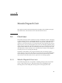
Typical System Partition
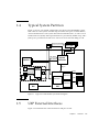
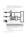
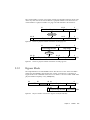
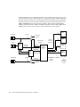
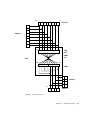
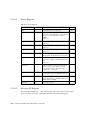
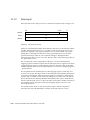
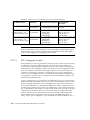
Figure 1-1 shows one possible configuration of U2P in a PCI UltraSPARC system.
U2P connects to the system controller chip and other UPA ports via UPA address,
control and data busses. The system has both PCI and EPCI slots, as well as an on
board PCI device (PCIO). Interrupt information is provided by the RIC chip, and a
JTAG port is provided for board test as well as in-circuit test and debug of U2P.
Memory Data (256+32ECC)
Memory SIMMs
XB1
UPA_D0(127:0+ECC)
UPA/S 64b
UPA_A0(35:0)
Graphics
Memory Address
Memory Control
UPA_D1(63:0+ECC)
UPA_A1(35:0)
System
Controller
UPA_Ctrl
TA(15:0)
Tag
TD(24+3+P)
Ultra
SPARC
DA(18+16BE)
PCI Bus
Clk
D(128+16P)
PCI Interface A
512KB
E$
UDB
PCI Bus
UPA Interface
PCI Interface B
RIC
Figure 1-1
1.5
PCIO
U2P
Typical PCI UltraSPARC System Block Diagram
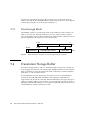
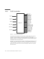
U2P External Interfaces
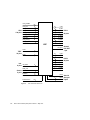
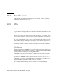
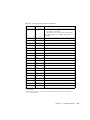
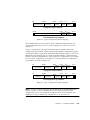
Figure 1-2 summarizes the external interfaces and pins of U2P.
Chapter 1
Overview
1-5
UPA
130 pins
UPA_DataBus
64
UPA_ECC
8
64
A_AD
UPA_Addressbus
UPA_Arbitration
36
2
A_PAR
6
8
A_C/BE#
UPA_P_Reply
5
7
A_CTRL
UPA_P_Reply
5
4
A_REQ#
UPA_Misc
3
4
A_GNT#
4
A_IDSEL
2
A_ERR
UPA_Reset_L
UPA_Sys_Clk
2
A_CLK
U2P
PCI_RST
TEST
10 pins
Intr.
6 pins
JTAG
5
MISC
5
INT_NUM
6
64
B_AD
2
B_PAR
8
B_C/BE#
7
B_CTRL
6
B_REQ#
6
B_GNT#
2
B_ERR
B_CLK
TMR_CLK
Clocks
5 pins
PSYCLK
2
BYPASS
2
VSSA
Power/Ground
Figure 1-2
1-6
104
U2P External Interfaces
UPA to PCI Interface (U2P) User’s Manual • May 1997
PCI A
96 pins
2
VDDA
5
VDD5
Shared
PCI RST
1 pin
PCI B
96 pins
Special
pwr/gnd
8 pins
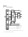
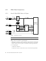
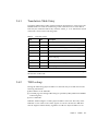
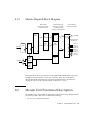
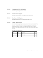
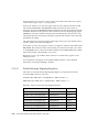
1.6
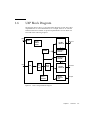
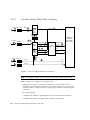
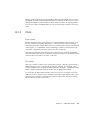
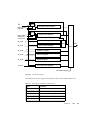
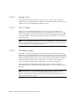
U2P Block Diagram
The diagram below shows a conceptual block diagram of U2P. The actual
implementation is somewhat different, for example, there are no internal
bidirectional busses. Details of specific implementation of each block can
be found in the following chapters.
JTAG
JTAG
PIO Ctl.
DMA Ctl.
BUS Ctl.
PCI Bus
Module A
IOMMU
PCI Bus A
Streaming
Cache A
Streaming
Cache B
UPA
UPA
ECC
Gen/
Check
Merge
Buffer
Timer/
Counters
Figure 1-3
PCI Bus B
PCI Bus
Module B
Mondo
Dispatch
Unit
Interrupts
U2P Conceptual Block Diagram
Chapter 1
Overview
1-7
1.7
U2P Block Overviews
This section gives a brief description of each top level functional block. A more
detailed description of each block can be found in Chapter 3. Each block is also
described in its own individual chapter as well. The top level blocks in U2P fall into
one of five categories:
1.7.1
■
UPA.
■
PCI.
■
Interrupt.
■
Internal Control.
■
Miscellaneous.
UPA Interface blocks
The UPA is UltraSPARC system’s packet switched main system bus. In an
UltraSPARC system, the UPA can operate up to 100 MHz. Data and address have
independent flow controls. Each type of UPA cycle (PIO read, PIO write, DMA read,
etc.) uses its own FIFO-based queueing. There is a synchronization boundary
between the UPA interface blocks and other U2P blocks, which run at 66.7 MHz.
1.7.2
■
UPA Master/Slave: This block deals exclusively with UPA address control. It
listens to UPA_A when U2P is a slave. It also arbitrates for and drives UPA_A
when U2P is a master.
■
UPA_Reply: This block deals exclusively with UPA data. It generates P_REPLY to
the System Controller (SC) ASIC during PIO and copyback cycles. It also listens
to S_REPLY from the SC and manages the UPA data FIFOs accordingly.
■
ECC Generate: Generates ECC on the outgoing 64-bit UPA data path.
■
ECC Check: Checks ECC on the incoming 64-bit UPA data path.
PCI Interface blocks
■
1-8
PCI Bus Module (PBM): This is the main portion of the PCI interface. U2P
contains two nearly identical copies of this block. One is designed to support a
64-bit PCI bus at 66 MHz or 33 MHz with up to four master devices. The other
supports a 64-bit PCI bus at 33MHz with up to six master devices. The PBM
adheres to all PCI protocol guidelines as contained in the PCI Revision 2.1
UPA to PCI Interface (U2P) User’s Manual • May 1997
specification. Each PBM controls arbitration, flow control and error handling for
its bus segment. Each PBM also handles the big- to little-endian byte twisting
required for correct operation of both PIO and DVMA datapaths.
1.7.3
■
IOMMU: For the portion of the PCI memory address space which is reserved for
DMA to the UPA bus, the IOMMU maps the PCI address into the appropriate
UPA physical address. The IOMMU keeps the 16 most recently used translations
in a TLB, and automatically performs hardware tablewalks on TLB misses. There
is a single IOMMU supporting both PCI busses. Only a single translation can be
in progress at a time, and during tablewalks, translations from the other bus
segment will be delayed.
■
Streaming Cache: The Streaming Cache (STC) is used to accelerate PCI DMA
activity. For DMA reads, the STC will speculatively prefetch 64-byte cache lines.
For DMA writes, the STC buffers up 64-byte lines before sending to the UPA
interface. There are two separate STC blocks in U2P, one associated with each
PBM block. Each STC contains storage for 16 virtual address tagged entries and
their data, which is stored in 64-byte lines, allocated on a least recently used basis.
Interrupt block
■
1.7.4
Mondo Dispatch Unit (MDU): In the Sun-4U architecture, interrupts to a
processor are sent as packets on the UPA bus. The MDU in U2P is a system
resource for generating such packets. The MDU accepts interrupt requests from
the UPA slave ports, PCI busses and internal U2P sources and dispatches
interrupt packets to the UPA.
Internal Control
■
Merge Buffer: In order to allow sub-line writes into a 64-byte memory line, it is
necessary to perform a read-modify-write operation on the UPA. The Merge
Buffer is responsible for generating the correct UPA read, merging the partial line,
and writing the whole block to the UPA.
■
PIO Control: Decodes slave requests from the UPA_A request FIFO, arbitrates for
the appropriate resource and dispatches the request.
■
Bus Control: This is an internal arbiter shared by the PIO Control and DMA
Control blocks. It schedules the use of the main internal data paths.
■
DMA Control: Arbitrates and decodes requests from internal DMA sources
(PBM, STC, IOMMU, MDU), and arbitrates for the appropriate UPA FIFO.
Chapter 1
Overview
1-9
1.7.5
Clock Ratios
At times it is desirable to run the clocks at less than their intended frequencies. Such
instances might be using the part in a low speed emulation environment, or if on
power up the clocks are defaulted to something other than their usual speed.
There are two ratios that must be adhered to:
■
UPACLK > 0.9 * PSYCLK if Mode bit = 1 (Control/Status Reg bit 0).
Prevents underrunning the UPA input FIFO which could occur if UPACLK is
running too slow in relation to PSYCLK.
■
PSYCLK > 0.41 UPACLK.
Prevents underrunning the DMA write data FIFO which could occur if PSYCLK is
running too slow in relation to UPACLK.
Note that it is clock ratios which are being specified here and not a minimum
operating frequency. U2P has been used in emulation at speeds in the 1KHz
range.
1.7.6
1.8
Miscellaneous
■
Timer/Counter: Contains two identical 32-bit timer-counters as specified by the
Sun-4U architecture. Used for system scheduling and profiling.
■
JTAG Control: Provides the necessary control for the standard IEEE 1149.1 JTAG
port, as well as additional scan based features that are useful for debugging
purposes.
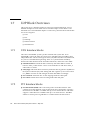
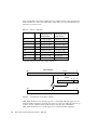
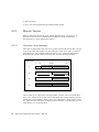
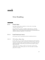
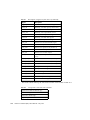
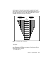
PCI Address Map Overview
Complete information on address maps and other software visible features of U2P
can be found in Chapter 13. A simplified diagram showing PIO and normal DVMA
address spaces is in Figure 1-4.
1-10
UPA to PCI Interface (U2P) User’s Manual • May 1997
1.f000.0000
PROM via PCIO
DVMA
PCI B Mem Space
xxx0.0000
Unused
8000.0000
1.8000.0000
PCI B Space
PCI A Mem Space
U2P
IOMMU
0000.0000
PCI bus B
memory space
1.0000.0000
DVMA
Unused
xxx0.0000
0.0202.0000
0.0201.0000
0.0200.0000
Unused
PCI B I/O Space
PCI A I/O Space
8000.0000
PCI A&B Config Space
0.0100.0000
U2P internal regs
PCI A Space
UPA Address
0.0000.0000
U2P UPA
address space
Figure 1-4
0000.0000
PCI bus A
memory space
U2P PIO and DVMA address spaces
Chapter 1
Overview
1-11
1-12
UPA to PCI Interface (U2P) User’s Manual • May 1997
CHAPTER
2
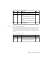
U2P Pin Descriptions
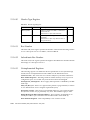
2.1
UPA Interface Signals
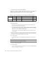
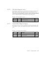
These signals connect U2P to the UPA. Maximum frequency of operation is 100 MHz.
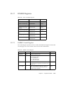
Table 2-1
UPA Interface Signals
Signal Name
Pin
Count
I/O
Description
UPA_DataBus
64
I/O
64 bit Data Bus
UPA_ECC
8
I/O
8 bits for ECC
UPA_Addressbus
36
I/O
Address/request lines + parity
UPA_Req_in
3
I
Requests from other clients on this address bus
UPA_Req_out
1
O
Request asserted by U2P
UPA_SC_Req_in
1
I
Request from the SC
UPA_Arb_Reset_L
1
I
UPA Arbiter reset
UPA_Addr_Valid
1
I/O
UPA_ECC_Valid
1
I
ECC Valid
UPA_Data_Stall
1
I
Data Stall
UPA_P_Reply
5
O
Port Reply signals
UPA_S_Reply
5
I
System Reply signals
Valid address; active high
2-1
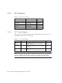
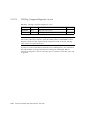
Table 2-1
UPA Interface Signals (Continued)
Signal Name
Pin
Count
I/O
UPA_Reset_L
1
I
Port/System Reset Signal
UPA_Sys_Clk_pos
UPA_Sys_Clk_neg
2
I
UPA System Clock (PECL)
UPA Total
2.2
Description
130
64-bit, 66MHz capable PCI Interface
Signals (PCI Bus A)
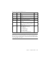
These signals connect U2P to the 64-bit, 66MHz capable PCI bus segment. Maximum
frequency of operation is 66.7 MHz.
Table 2-2
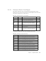
PCI Bus A signals
Signal Name
2-2
Pin Count
I/O
A_AD<63:0>
64
I/O
Address/Data Bus
A_PAR
1
I/O
Parity for AD<31:0>
A_PAR64
1
I/O
Parity for AD<63:32>
A_CBE_<7:0>
8
I/O
Command/Byte enable lines
A_FRAME_
1
I/O
Cycle frame
A_REQ64_
1
I/O
Request 64-bit transfer
A_ACK64_
1
I/O
Acknowledge 64-bit transfer
A_TRDY_
1
I/O
Target Ready
A_IRDY_
1
I/O
Initiator Ready
A_STOP_
1
I/O
Target initiated STOP
A_DEVSEL_
1
I/O
Target decoded its address
A_IDSEL<3:0>
4
O
A_PERR_
1
I/O
Parity Error
A_SERR_
1
I/O
System Error
A_CLK
1
I
UPA to PCI Interface (U2P) User’s Manual • May 1997
Description
Chip select lines for configuration cycles
PCI Clock
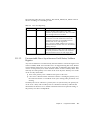
Table 2-2
PCI Bus A signals (Continued)
Signal Name
2.3
Pin Count
I/O
Description
A_REQ_<3:0>
4
I
Bus master request lines
A_GNT_<3:0>
4
O
Bus master grant lines
PCI_RST_
1
I
Reset (shared with PCI bus B)
PCI Bus A total
97
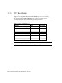
64-bit, 33MHz PCI Interface Signals (PCI
Bus B)
These signals connect U2P to the 32-bit PCI bus segment. Maximum frequency of
operation is 33.3 MHz.
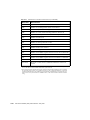
Table 2-3
PCI Bus B Signals
Signal Name
Pin Count
I/O
Description
B_AD<63:0>
64
I/O
Address/Data Bus
B_PAR
1
I/O
Parity for AD<31:0>
B_PAR64
1
I/O
Parity for AD<63:32>
B_CBE_<7:0>
8
I/O
Command/Byte enable lines
B_FRAME_
1
I/O
Cycle frame
B_REQ64_
1
I/O
Request 64-bit transfer
B_ACK64_
1
I/O
Acknowledge 64-bit transfer
B_TRDY_
1
I/O
Target Ready
B_IRDY_
1
I/O
Initiator Ready
B_STOP_
1
I/O
Target initiated STOP
B_DEVSEL_
1
I/O
Target decoded its address
B_PERR_
1
I/O
Parity Error
B_SERR_
1
I/O
System Error
B_CLK
1
I
PCI Clock
B_REQ_<5:0>
6
I
Bus master request lines
Chapter 2
U2P Pin Descriptions
2-3
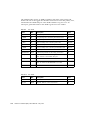
Table 2-3
PCI Bus B Signals (Continued)
Signal Name
2.4
Pin Count
I/O
Description
B_GNT_<5:0>
6
O
Bus master grant lines
PCI_RST_
0
I
Reset (shared with PCI bus A)
PCI Bus B total
96
Miscellaneous Interfaces
Clocks, interrupts, JTAG interface, and other test pins.
Table 2-4
Miscellaneous Signals
Signal Name
2-4
Pin Count
I/O
PSYCHOPS_CLK
1
I
66 MHz main clock
PSYCHOPS_CLKR
1
I
Reference pin for PSYCHOPS_CLK
PSY_BYPASS
1
I
Bypass PLL on PSYCHOPS_CLK
UPA_BYPASS
1
I
Bypass PLL on UPA_Sys_Clk
TMR_CLK
1
I
10 MHz timer/counter clock
INT_NUM
6
I
Encoded interrupt number
BOOT_BUS
1
I
Select PCI bus A or B for system boot path
EXT_EVENT
1
I
External event trigger
INT_EVENT
1
O
Internal event trigger
B_CPU_REQ
1
O
Test signal - copy of PBMB internal request
B_CPU_GNT
1
O
Test signal - copy of PBMB internal grant
JTAG
5
I/O
Misc. total
21
UPA to PCI Interface (U2P) User’s Manual • May 1997
Description
JTAG test port
2.5
Power and Ground Pins/Pads
Each signal pin (or ball) is directly connected to a pad on the U2P die. Power and
ground pins are connected to power and ground planes on the package substrate.
Power and ground pads on the die are connected to these planes as well, but there is
no 1-1 correspondence between power/ground pads and pins.
Table 2-5
Power and ground pins
Signal Name
Pad
Count
Pin
Count
Description
VDD
52
32
3.3V power supply
VSS
52
72
Digital ground
Power total
104
104
In addition to the main power and ground pins, U2P has some special purpose
power and ground pins. These are treated as signal pads/balls, and there is no
special handling on the package substrate.
Table 2-6
Special power and ground pins
Signal Name
Pad
Count
Pin
Count
Description
VDD5
5
5
5V reference voltage
VDDA
2
2
3.3V analog supply
VSSA
1
1
Analog ground
Special total
8
8
Chapter 2
U2P Pin Descriptions
2-5
2.6
Total Pin/Pad Count
Total Pin Count
Table 2-7
Interface
2-6
Pad Count
Pin Count
UPA
130
130
PCI Bus A
97
97
PCI Bus B
96
96
Miscellaneous
21
21
Special Power/Ground
8
8
Subtotal
352
352
Power/Ground
104
104
Total Count
456
456
UPA to PCI Interface (U2P) User’s Manual • May 1997
CHAPTER
3
U2P Functional Description
3.1
Functional Overview
This chapter contains the functional description of the U2P chip at the top level.
Overall chip design is discussed and the address data/flow is presented. This
chapter has 2 major sections:
3.2
■
Block diagrams of the address and data paths.
■
A description of each of the major design blocks within U2P.
Top-Level Architectural Philosophy
When reviewing the U2P internal bus structure, it is important to keep in mind the
architectural philosophy of the chip:
■
U2P has a UPA bus.
■
U2P has two PCI busses.
■
The design connects them together so that data goes as fast as possible without
making the chip too complicated.
■
Where practical, the UPA to SBus (U2S) chip design has been leveraged.
3-1
UPA Interface
UPA
UPA
Addr.
input
U2P Header
U2P_PA
41
UPA
Data
input
PIO WR Fifo
Stream
Cache
A
U2P_PD
64
Addr/
Data
PBM
A
Ctrl.
UPA_PD
STCA_PD
PBMA_PD
UPA
Data
output
PIO RD Fifo
STCB_PD
P2U_PD
PBMB_PD
64
DSB_PD
Stream
Cache
B
MDU_PD
Addr/
Data
PBM
B
MMU_PD
P_REPLY
Ctrl.
ECC_PD
P_REPLY
output
TMR_PD
PRP Mux
DMA
CTL
MDU
IO
MMU
UPA Interface
Blocks
Internal PIO
Slaves
ECC
Timer
Counter
Figure 3-1
3-2
PIO Data & Address Paths
UPA to PCI Interface (U2P) User’s Manual • May 1997
41
UPA Interface
P2U_DA
P2U Header
UPA
Addr.
output
41
S_REPLY
input
S_REPLY
DRQA Mux
PBMA_DA
STCA_DA
PBMB_DA
STCB_DA
MRG_DA
MDU_DA
MMU_DA
64
PBM
A
Ctrl.
64
41
64
DMA
CTL
64
Stream
Cache
A
41
DMA WR Fifo
UPA
Data
output
P2U_DD
64
DMA RD Fifo
UPA
Data
input
PCI
Addr/
Data
DRQD Mux
PBMA_DD
STCA_DD
PBMB_DD
STCB_DD
MRG_DD
MDU_DD
64
PCI
PBM
B
Addr/
Data
Ctrl.
64
41
64
U2P_DD
64
64
Stream
Cache
B
41
64
64
DMA
Merge
Buffer
64
41
MDU
64
UPA Interface
Blocks
Figure 3-2
40
Internal DMA
Masters
64
IO
MMU
DMA Data & Address Paths
Chapter 3
U2P Functional Description
3-3
3.3
Block Overviews
3.3.1
PIO Decoder
This block decodes requests from the U2P header request FIFO. The target of the PIO
cycle may be either PCI bus or one of the internal U2P units. For PCI, the
corresponding PBM will determine the transaction timing based on the response of
the PCI device. For internal units, the PIO Decoder and Bus Controller block control
the timing. All PIO requests are serviced strictly in order and one at a time.
For PIO accesses to PCI configuration space, the PIO Decoder does not have enough
information to determine which PBM receives the transaction. With the help of the
Bus Controller block, the PIO Decoder will forward the request to both PBM
modules. Based on the values programmed into the Bus Number and Subordinate
Bus Number registers in each PBM, one or none of the PBM’s will accept the PIO,
and the Bus Control unit will correctly handle the situation.
The PIO decoder allows the following transaction types:
3.3.2
■
P_NCBRD_REQ, P_NCBWR_REQ - Only to PCI memory space portion of address
space, not to U2P internal address space or PCI config or PCI I/O space.
■
P_NCRD_REQ - With byte masks representing 1, 2, 4, or 8-byte aligned accesses
to any U2P internal register.
■
P_NCRD_REQ - With byte masks representing 1, 2, or 4-byte aligned accesses to
PCI I/O or PCI Configuration space.
■
P_NCRD_REQ - 1, 2, 4, 8, or 16-byte accesses are allowed to PCI memory space.
■
P_NCWR_REQ - 8-byte accesses are allowed to U2P internal registers (less than 8byte access is allowed, but treated as 8 bytes).
■
P_NCWR_REQ - 4-byte or less accesses are allowed to PCI I/O or PCI
Configuration Space.
■
P_NCWR_REQ - Any arbitrary byte mask is allowed to PCI memory space.
DMA Control
This block decodes and builds the UPA packet for requests from PCI bus A or B,
streaming cache A or B, the IOMMU, the Mondo Dispatch Unit or the Merge Buffer.
This block also keeps a FIFO of the requests. All DMA transactions are issued on the
UPA with the class bit set to 0, so the UPA will service U2P DMA requests in order.
U2P is capable of generating the following transaction types:
3-4
UPA to PCI Interface (U2P) User’s Manual • May 1997
3.3.3
■
P_NCBRD_REQ, P_NCBWR_REQ - From PBM blocks only.
■
P_NCWR_REQ - From PBM block only, may have arbitrary byte mask.
■
P_RDO_REQ, P_WRB_REQ - From merge buffer for partial line DMA writes.
■
P_RDD_REQ - From PBM, STC or IOMMU.
■
P_WRI_REQ - From PBM or STC.
■
P_INT_REQ - From Mondo Dispatch Unit.
Bus Control
This is an internal arbiter shared between the DMA Control and PIO Control units.
The bus control unit handles timing of internal U2P resources based on the number
of clocks required for each kind of transaction. The bus control unit correctly handles
“ambiguous” PIO destinations (i.e. PIO’s to PCI configuration space, in which either
or none of the PBM blocks may respond).
There are separate busses for each of the following operations: PIO read, PIO write,
DMA read and DMA write. The PIO read and write busses are considered a single
resource by the bus controller, so only one PIO operation is in progress at a time. The
remaining busses are independent, however, so the bus controller allows a PIO
operation, a DMA read, and a DMA write all to be in progress at the same time.
The bus controller also handles allocation of the merge buffer. A DMA write that
requires the merge buffer is held off until it is available. Once the merge buffer is
allocated, the bus controller will not allow any other DMA operation to be initiated
until the merged data is written back to the UPA.
3.3.4
UPA Master / Slave
The UPA Master / Slave (UMS) block is U2P’s interface to the UPA_A request bus.
When U2P is addressed as a UPA slave (PIO requests), the UMS always writes the
request into the U2P Header FIFO.
When U2P is performing a DMA request, the UMS arbitrates for use of the UPA_A
bus and drives the request out from the P2U Header FIFO.
As with the UPA Reply block, the UMS runs at the UPA clock frequency, up to 100
Mhz. Signals from other internal U2P blocks are 2-clock synchronized by the UMS
before being used. Likewise, status and control which is an output of the UMS block
is 2-clock synchronized with the U2P main clock (66.7 Mhz) before being used.
Chapter 3
U2P Functional Description
3-5
3.3.5
UPA Reply
The UPA Reply unit manages replies to the system controller. P_REPLY requests are
received from the PIO Control Unit and forwarded to the UPA bus. For PIO reads,
P_REPLY indicates that U2P has read data ready in the PIO_RD FIFO. For PIO
writes, P_REPLY indicates that U2P has removed write data from the PIO_WR FIFO.
P_REPLY is not used for DMA.
S_REPLY is used for both PIO and DMA cycles. For PIO reads, S_REPLY indicates
that the system controller is ready to read data out of the PIO_RD FIFO. For PIO
writes, S_REPLY indicates that data is being written into the PIO_WR FIFO. For
DMA reads, S_REPLY indicates that data is being delivered into the DMA_RD FIFO,
and for DMA writes, S_REPLY indicates that the system controller is ready to read
data out of the DMA_WR FIFO.
The UPA Reply unit is responsible for reading and writing the appropriate data
FIFO’s and enabling the UPA Data outputs if necessary. In addition, the UPA Reply
unit must control the ECC check logic. When data is arriving at U2P (related to a
PIO write or DMA read), the data is ECC checked. The UPA Reply unit must
accumulate the ECC results for the entire packet, which may be between 1 and 64
bytes in length. The UPA Reply unit manages a separate packet status FIFO which
signals the PIO and DMA CTL units of error conditions.
3.3.6
ECC Generate / Check
The ECC unit is split into separate generate and check functions. ECC is always
calculated on 64 bits of data. The ECC generate logic is positioned on the “internal”
side of all of the data FIFO’s. (There is not enough time between receiving S_REPLY
and providing data to generate the ECC if the logic is on the UPA side of the FIFO.)
This also allows more flexibility in the circuit timing since the UPA clock is faster
than the internal U2P clock. In some situations, it is necessary for U2P to generate
intentionally bad ECC with the data. When this is needed, bits [1:0] of the outgoing
ECC are inverted to provide a guaranteed Uncorrectable Error.
The ECC check logic will detect Correctable and Uncorrectable ECC errors. (CE and
UE errors.) Refer to the ECC chapter for the rules for detecting and correcting errors.
For a correctable error, the data will be repaired before being sent to the internal
destination block. None of the internal U2P units will be aware of CE errors. For
both UE and CE errors, the ECC unit will signal the Mondo Dispatch Unit to
generate a Mondo Vector (interrupt) if enabled.
3-6
UPA to PCI Interface (U2P) User’s Manual • May 1997
3.3.7
DMA Merge Buffer
The DMA Merge Buffer block is used for servicing cacheable DMA Writes of less
than 64 bytes (partial writes). This is required in a UPA based system because there
is no way to write cacheable memory in sub-line increments. (There are at least 2
problems that force this; the SIMMS do not have individual byte controls and ECC is
generated on 8-byte boundaries.). In order to perform a sub-line write, U2P performs
a UPA Read-to-Own (P_RDO_REQ) transaction to gain control of the line, merge the
new data into the line and then flush the line to memory with a UPA Writeback
(P_WRB_REQ) transaction. Once the Merge Buffer’s request for a Read-to-Own
transaction is granted internally, no other DMA requests will be serviced until the
writeback completes.
The only blocks capable of partial writes are the two PBM’s and the two streaming
caches. The Merge Buffer contains a 64-byte buffer for storing the partial line while
waiting for data from the P_RDO_REQ transaction. There are valid bits for each byte
in the buffer, so it is able to handle completely arbitrary byte enables on a consistent
write from a PCI device. Although the merge buffer could also handle arbitrary byte
enables on a streaming access, U2P does not support this because the streaming
cache only stores a begin and end pointer for valid data, and not individual byte
enables.
To avoid the complexity of having to participate in system coherence during a
merge, the external system controller is responsible for blocking all requests to the
line for which U2P has issued a Read-to-Own until the data merge is completed and
U2P has issued a Writeback of the line to memory. U2P will not issue any other
transactions between the Read-to-Own and the Writeback.
The DMA Merge Buffer is not intended to be a high performance solution for subline DMA writes from a PCI bus; rather its purpose is to provide correct
functionality given the UPA bus constraints. The streaming cache (STC) can be used
to improve PCI performance by buffering data into 64-byte lines before flushing to
memory. STC line flushes that contain a complete 64 bytes will be able to bypass the
Merge Buffer by doing a Write Invalidate (P_WRI_REQ) on the UPA.
3.3.8
PCI Bus Module (PBM)
Each PCI Bus Module block implements a complete PCI Master and Slave interface.
Each PBM implements all of the required host bridge functions for PCI, and also acts
as the central resource for: arbitration, reset, and system error (SERR#) monitoring.
The PBM handles the timing of PIO requests to the PCI bus. These are handled one
at a time. The PBM handles target disconnects, retries and various error conditions
during the PIO. If necessary, multiple PCI transactions will be generated for each
Chapter 3
U2P Functional Description
3-7
PIO (up to 16 transactions in the case of 64-byte block reads or writes). While the
multiple transactions of a single PIO are occurring on the PCI bus, DMA requests
from other devices on that bus can be still be serviced.
Only 1, 2, 4, 8, 16 or 64-byte aligned PIO read accesses are allowed to the PCI bus
Memory Space. Writes to the PCI bus Memory Space may be of any size supported
on the UPA. For most PIO’s, the command used on the PCI bus will be Memory
Read or Memory Write. 64-byte PIO reads will use the Memory Read Line
command. Other command types can be generated by PIO’s to special regions in the
PCI address space. These include the Configuration Read, Configuration Write, I/O
Read, I/O Write, and Special Cycle commands. With these command types, only 4byte or smaller PIO’s are supported.
The PBM also responds as a target to other PCI masters. The PBM will respond to
any PCI Memory Space transaction for which address bit 31 is on. Typically, the
transaction address is treated as a virtual address, and translated to a physical
address by the IOMMU. These transactions are referred to as DVMA transactions.
The PBM communicates with the IOMMU and STC blocks as needed to complete
DVMA cycles to/from the PCI bus. (An IOMMU bypass mode is also available,
which can directly access the entire UPA physical address space using PCI DualAddress Cycles.) DVMA data can be moved from the PCI bus to either the
associated STC or directly to the UPA. Peer-to-peer DMA is also allowed between
two devices on the same PCI bus segment, but due to the way PCI addressing is
defined, U2P is not involved in these transfers (except as the central arbiter for bus
request and grant signals).
The PBM will only respond, as a target, to PCI memory space commands (Memory
Read, Memory Read Line, Memory Read Line Multiple, Memory Write, and Memory
Write & Invalidate). All other PCI command types are ignored.
All PCI transactions targeting U2P will be disconnected by the PBM if the master
attempts to cross a 64-byte boundary. Under certain conditions, the PBM will issue a
retry for an incoming PCI transaction. These conditions include:
■
■
■
PBM requests the IOMMU to do a tablewalk to get mapping for this
transaction.
STC indicates that it is initiating a request to get the desired read data.
Due to congestion, resources (buffers) are currently lacking to accept a
transaction.
For DVMA transactions to cacheable memory, based on the IOMMU mapping
information for the virtual address, the PBM will treat the DVMA cycle as a
consistent or streaming access (accesses made in IOMMU bypass mode are always
treated as consistent). Consistent accesses are sent directly to the UPA and have
strict ordering constraints; The performance of consistent accesses can be worse than
streaming accesses (particularly for reads or sub-line writes), and DVMA pages
should only be marked consistent-mode when necessary. DVMA accesses to noncacheable memory is always treated in consistent mode.
3-8
UPA to PCI Interface (U2P) User’s Manual • May 1997
For consistent DVMA reads, the PBM treats all three PCI memory read commands
identically. For streaming reads, the PBM passes the information on which command
was used to the streaming cache so that a decision can be made on prefetching data.
For all DVMA write transactions, both PCI memory write commands are treated the
same.
For DVMA reads, the DVMA master may drive arbitrary byte enables on the PCI
bus, which will be ignored. DVMA reads always generate 64-byte requests on the
UPA bus, and correct data is returned for all byte lanes on the PCI bus, regardless of
the byte enables.
For consistent DVMA writes, arbitrary byte enables are also allowed. The byte
enables for the transaction are stored along with the data, and are passed on to the
Merge Buffer for partial line writes to cacheable space. For non-cacheable partial
writes, the byte enables are passed on to the Bus Controller/DMA Controller, which
uses them for the Bytemask field of the outgoing P_NCWR_REQ packet(s).
For streaming DVMA writes, arbitrary byte enables are not allowed. Within a single
PCI transaction, all data must be contiguous bytes. If any byte holes are detected, the
PBM will set a status bit, and an interrupt will be generated if enabled. Meanwhile,
the transaction continues as if the byte hole were not there, and the appropriate byte
enables were on. This will cause incorrect data to be eventually be written to
memory for these bytes. This only applies to a single continuous PCI transaction gaps between the end address of one transaction and the start address of the next are
allowed, and correctly handled by the streaming cache (although they may cause
performance degradation).
The PBM also helps to enforce certain ordering constraints between consistent
DVMA writes (cacheable or non-cacheable) and the following synchronization
events:
■
PIO reads of PCI registers.
■
Interrupts.
■
Other consistent DVMA writes (e.g. a descriptor update).
For PIO reads (to PCI space, not internal registers), the PBM for the targeted bus
communicates with the DMA Controller to ensure that all of its previous consistent
DVMA writes have completed before allowing the PIO to complete.
For PCI related interrupts, the MDU notifies the appropriate PBM when an interrupt
is received. The PBM then notifies the MDU when all of its outstanding consistent
DVMA writes have been flushed. The MDU will not generate the interrupt packet
until the PBM has flushed data.
Descriptor updates are correctly handled by the strict ordering of all consistent
DVMA accesses.
The only PCI bus function that is not handled by the PBM is the interrupt logic. This
is contained in the MDU block.
Chapter 3
U2P Functional Description
3-9
3.3.9
IOMMU
This block is used for PCI DVMA cycles. It maps 32-bit PCI Virtual Addresses to 41bit UPA Physical Addresses for both PBM blocks. There is a single 16-entry
Translation Look-aside Buffer (TLB) to cache recently used translations. The TLB
entries are replaced on an LRU basis, without regard to the bus of origin. The
IOMMU can provide 2 levels of service when a PBM presents a virtual address for
translation:
■
First, the IOMMU examines the TLB to see if a translation for the virtual address
is already available.
■
If there is a miss in the TLB, the IOMMU block will perform a HW table-walk to
get the translation if requested by the PBM (since the PBM also checks the
streaming cache for a translation, this may not be necessary). The IOMMU does
this by reading from the TSB table by issuing a DMA read to main memory. This
is only a single-level table search, unlike previous Sun MMU models.
The IOMMU allows only a single translation to be in progress at a time. This
includes the tablewalk portion of a translation, so if one PBM has requested a
tablewalk, translation requests from the other PBM are held off until the tablewalk
completes.
In the case of simultaneous translation requests by both PBM’s, priority is given to
PBM A.
3.3.10
Streaming Cache
Each Streaming Cache (STC, but sometimes referred to as a Streaming Buffer) is used
to accelerate DVMA traffic to/from its associated PCI bus. It contains a pool of 16
64-byte entries. These entries are tagged by virtual page number, and are managed
as a fully-associative cache. Only one entry will be valid for any given virtual page.
Entries are assigned as needed by the STC logic. An LRU algorithm is used to assign
new pages to entries when all of the entries are valid. All 16 entries are available for
either read or write streams, although at a given time, each entry is only valid for a
single direction.
For DVMA writes, the STC will buffer up data in an entry until a 64 byte has been
reached. The STC will then flush the completed line into a flush buffer. As soon as
the internal busses are available, data in the flush buffer is sent to the UPA block.
The flush is guaranteed to occur if the last word of the line has been written - there
is no possibility of a completed dirty line being left in the streaming cache for an
indeterminate amount of time. For DVMA reads, the STC will often be able to
prefetch a new 64 byte line into a prefetch buffer, and then copy it into the correct
streaming cache entry before it is needed by the requesting device. This prefetch is
initiated whenever the Memory Read Line or Memory Read Line Multiple
commands are used on the PCI bus, as signalled to the STC by the PBM, and there is
3-10
UPA to PCI Interface (U2P) User’s Manual • May 1997
not already an outstanding prefetch request waiting for data. A prefetch is also
initiated if it has not already been issued and the last word of a line is read.
Prefetches are never issued when a page boundary is reached.
The STC expects that the DVMA device is accessing data in sequential and
increasing order, without any byte holes. If the actual device access pattern is
different, the STC, in concert with the PBM, will maintain data correctness but the
performance gains will not be as high. One exception to data correctness is if a
device generates byte-holes within a single write transaction. When this happens,
the byte enables in the byte hole are treated as if they were on (thus possibly causing
data corruption), and a Streaming Byte Hole Interrupt is signalled (if enabled).
Data which is stored in the STC does not participate in the UPA cache coherence
protocol. The STC implements a flush command to allow system software to
explicitly remove virtual pages from the STC when a DVMA transfer is done or
when an IOMMU demap operation occurs. In order to ensure that the STC flush
data has reached UPA memory, a special synchronization register is provided.
The two streaming caches in U2P do not communicate with each other. There is no
snooping done to determine if the same virtual page is in use in both caches. It is up
to software to ensure that either no devices from separate busses access the same
virtual page in streaming mode, or, if they do, that they do not access the same 64byte lines within the page. (Note that the same warning applies to having multiple
virtual addresses in either or both streaming caches map to the same physical
address.)
3.3.11
MDU
The Mondo Dispatch Unit is U2P’s vehicle for dispatching Interrupt packets to an
Interrupt Handler on the UPA bus (primarily a CPU). The MDU will generate a
special type of UPA packet (a Mondo Vector, P_INT_REQ). The MDU block accepts
external interrupt requests from PCI or UPA devices (encoded onto a 6-bit
INT_NUM bus) as well as internal U2P interrupt sources and dispatches Interrupt
packets to the UPA. The contents and target of the interrupt packet are controlled
through the Interrupt Number Registers (INR) within the MDU. Each INR is 16 bits,
with 5 of these bits indicating the MID of the target CPU. For simplicity, no data
other than the interrupt number (INO) is sent in the 64-byte interrupt packet from
U2P (unused bits are all sent as 0s).
There are 38 external interrupt sources that can have their requests serviced through
the MDU. In order to conserve pins on U2P, these are handled by an external
interrupt concentrator (e.g. the RIC chip). The interrupt concentrator sends interrupt
requests to the U2P by encoding them onto a 6 bit interface.
Chapter 3
U2P Functional Description
3-11
Once an interrupt is received from the external concentrator, it is put into one of 2
groups, based on the least significant bit of the target MID programmed into the
corresponding INR (U2P is optimized for a system with 2 CPU’s, but can be used in
systems with up to 4 CPU’s). Within each of these groups, the MDU performs a
priority arbitration to determine which interrupt to send.
Before any PCI related interrupt packet is sent to the UPA, the MDU checks with the
appropriate PBM block to see if it has any posted consistent DMA write data. If so,
the MDU waits until the PBM indicates that the write data has been sent to the UPA
block.
The Mondo Interrupt packet is then sent to the target CPU using the same UPA
queue that is used for DMA writes. The Mondo packet can be either ACKed or
NACKed by the UPA. If the packet is NACKed (rejected), the CPU is already busy
servicing another Mondo. In this case, the MDU will resubmit the packet at a later
time based on a free-running retry interval counter. (This retry interval is
programmable.) In the meantime, Mondo packets can still be sent to other CPU’s (as
long as they differ in the LSB of the MID). To simplify the design, U2P can only have
one Mondo vector outstanding (i.e. waiting for ACK or NACK) at any time.
3.3.12
Timer / Counters
There are two identical, independent 29-bit timer/counters in U2P. Each can provide
either periodic interrupts or single-event interrupts to a selected processor. The
interrupt is delivered to the target CPU using a Mondo vector, and each counter can
target a different CPU. The counters are driven by the TMR_CLK input, which is
nominally at 10MHz. This clock is scaled down by a factor of 10 first, so the counters
will typically increment once a microsecond, which allows periodic interrupt
intervals of up to 536 seconds.
Each counter has an associated Limit Register, and a Periodic enable bit. When a
counter reaches its limit value, an interrupt is generated (if enabled). If the Periodic
bit is set, the count is reset to 0, otherwise it is left alone (the count is also reset to 0
whenever the Limit Register is written). To obtain a periodic interrupt every ‘N’
microseconds, the limit value should be set to ‘N-1’.
3.3.13
Reset
A synchronous reset is implemented in U2P. UPA_RST_L is the source of this reset
and it is distributed to 3 internal clock domains and to the PCI bus.
3-12
UPA to PCI Interface (U2P) User’s Manual • May 1997
To the UPA domain UPA_RST_L is registered on input and distributed to the various
modules within the domain. Each of those modules further registers the reset before
distribution to the destination flops. This gives a 3 cycle delay between the external
reset pin and the time the internal logic is reset.
In the PSYCLK domain UPA_RST_L will occur at the destination flops either 1 or 2
clocks from the time of it’s assertion. This is due to the fact that UPA_RST_L is based
in the UPACLK time domain and is thus asynchronous to the PSYCLK domain. The
de-assertion of UPA_CLK_L will occur at the destination flops a maximum of 3
PSYCLK cycles later. This is accomplished by sending UPA_RST_L through a dual
rank synchronizer which feeds an AND function, and at the same time by-passing
the synchronizer with UPA_RST_L to feed the other term of the AND function.
To the PCI bus, UPA_RST_L is asserted asynchronously and de-asserted
synchronously. This is accomplished using the dual rank synchronizer and AND
function described in the previous paragraph. The PCI signal PCI_RST_ will be
asserted in the same cycle as UPA_RST_L and will be de-asserted 2 PSYCLK cycles
after UPA_RST_L.
3.3.14
Testability
U2P has a JTAG (IEEE 1149.1) compliant TAP controller and boundary scan. In
addition, all internal functional flip-flops are scannable. Several other scan based test
and debug features are implemented as well, including Built-In Self-Test (BIST)
circuitry for internal memories that are not directly accessible via PIO accesses. The
Design-for-Testability (DFT) features of U2P are further documented in Chapter 12.
Chapter 3
U2P Functional Description
3-13
3-14
UPA to PCI Interface (U2P) User’s Manual • May 1997
CHAPTER
4
DMA/PIO Transactions Flow
This chapter describes the flow of DMA and PIO transactions through U2P’s UPA
(Unified/UltraSPARC Port Architecture) bus interface. The major generic blocks
involved in any DMA transaction are the Bus Controller, DMA controller, and UPA
bus interface (and the Merge Buffer for coherent DMA writes of less than 64 Bytes).
The major blocks involved in any PIO transaction are the Bus Controller, PIO
Decoder, and the UPA bus interface.
Figure 4-1 shows a top level block diagram of the interconnection between the
blocks responsible for DMA and PIO transactions control.
Note – This chapter assumes that the reader is familiar with the basics of the UPA
(Unified/UltraSPARC Port Architecture) Interconnect. Please refer to “UPA
Interconnect Architecture” Release 2.0, Document Part Number 960-1156-01.
4-1
4.1
Block Diagram
UPA BLOCK
PIO ADDR
PIO HDR
PIO
DECODER
UPA
MASTER/
SLAVE
ADDRESS
BUSSES
DMA CTRL.
DMA ADDR
DMA
REQUEST
DMA HDR
BUS CTRL.
PIO CTRL
PIO CTRL
UPA
ECC
SREPLY
DMA
Scoreboard
DMA CTRL
DMA CTRL
PIO
ARB/CTRL
DMA
ARB/CTRL
PIO CTRL
DMA CTRL
DMA
REPLY
PREPLY
UPA
REPLY
&
DATA
MERGE
BUFFER
DMA WR
DMA WRITE DATA
DATA
DMA RD
DMA READ DATA
DATA
DATA
BUSSES
PIO WR
PIO WRITE DATA
DATA
PIO RD
PIO READ DATA
DATA
Figure 4-1
4-2
Top level block diagram for DMA and PIO transactions flow/control
UPA to PCI Interface (U2P) User’s Manual • May 1997
■
UPA Block: This block is U2P’s interface to the UPA bus. It is composed of three
major sub-blocks:
a. UPA Master/Slave: This block is so called because it simultaneously operates
in two different modes, Master and Slave. In Master mode, it arbitrates for the
UPA bus and puts a UPA request on the UPA address bus after it wins
arbitration. In slave mode, it listens to the UPA address bus waiting for a
transaction.
b. UPA Reply/Data: This block contains all data FIFO’s needed to buffer DMA
and PIO data. It also handles P_REPLY and S_REPLY packets.
c. ECC: This block generates ECC on data sent from U2P to the UPA bus, and
checks ECC on data received from the UPA bus.
■
DMA Controller: This block is responsible for building DMA transaction packets
sent to the UPA bus and for keeping track of them. It is composed of three major
sub-blocks:
a. DMA Request: DMA requests from U2P’s internal blocks are sent to this block
under control from the Bus Controller. The DMA Request block then builds the
appropriate UPA transaction and inserts it in the DMA header FIFO in UPA
Master/Slave. At the same time it sends all information related to the DMA
transaction to the Scoreboard to be stored until the DMA transaction is
completely serviced (i.e., DMA read data has been received, or DMA write
data has been taken).
b. DMA Reply: The UPA Reply/Data block forwards all DMA related S_REPLY’s
to this block to be decoded. If the S_REPLY is related to an outstanding DMA
read, the DMA reply arbitrates for U2P’s internal busses to deliver the DMA
read data and removes the DMA request from the scoreboard. If the S_REPLY
is related to an outstanding DMA write, the DMA Reply just removes the
DMA write request from the scoreboard. This block also drives the appropriate
Ack and Nack signals to U2P’s internal blocks based on the S_REPLY type.
c. Scoreboard: The scoreboard keeps a record of all outstanding DMA
transactions to the UPA. It stores the following DMA related information:
i. Transaction direction (Read/Write).
ii. Cacheable bit to indicates transaction destination (memory vs. IO).
iii. 16-bit Byte Mask.
iv. ID of the block that initiated the DMA transaction.
v. Special field (4 bits) that can be used by the block which initiated the DMA
to store any type of information. The Streaming Cache, for example, stores
an index number to its 16 buffers. This index number is returned to the
streaming cache along with the DMA read data.
vi. DMA address (used for DMA read error recording).
Chapter 4
DMA/PIO Transactions Flow
4-3
■
PIO Decoder: The UPA Master/Slave passes UPA transactions to this block to be
decoded. The PIO Decoder extracts from the UPA transaction the PIO address,
destination, direction (read or write), byte mask, and transfer size. Outputs of this
block are used by the Bus Controller to initiate the PIO access internally.
■
Bus Controller: This block is in charge of concurrently coordinating DMA and
PIO transactions inside U2P. It is composed of three major sub-blocks. The first
one controls PIO transactions to all internal blocks. The second one is responsible
for arbitration between internal blocks and for passing DMA requests to the DMA
Controller. The third block communicates with the DMA Reply to deliver DMA
read data to the requesting block.
■
Merge Buffer: The merge buffer concept was introduced to eliminate the need for
U2P to participate in the UPA cache coherence protocol. Its main function is to
handle coherent DMA writes to main memory which are less than 64 Bytes. When
the Bus Controller detects that the size of the write transaction is less than 64
Bytes it informs the merge buffer. The merge buffer fetches the addressed data
block (64 Bytes) from the memory and merges the new data, then it writes the
data block back into the memory.
U2P’s internal blocks that issue DMA transactions destined for the UPA are called in
this chapter Requesting Sources or Blocks. These sources include the PBM Modules
(A & B), the Streaming Caches (A & B), the Merge Buffer, the Mondo Dispatch Unit
(Interrupts are treated as DMA Writes), and the IOMMU. Blocks that can be accessed
in slave mode (PIO) are called Destination Blocks. These blocks include, in addition
to all requesting blocks, the UPA interface, the ECC block, the Timer block, the
Scoreboard, and the Performance registers.
The acronyms below are used in the following sections:
4-4
■
DMA_HDR: A 70 bit DMA header which is basically the two cycles of a UPA
transaction (side by side) without the parity bits.
■
DMA_HDR FIFO: DMA Header FIFO used to buffer UPA transactions until U2P
wins the UPA bus arbitration.
■
DMA_WR FIFO: DMA Write Data FIFO.
■
DMA_RD FIFO: DMA Read Data FIFO.
■
P2U_DD: PCI-to-UPA DMA Data (DMA Write Data).
■
U2P_DD: UPA-to-PCI DMA Data (DMA Read Data).
■
P2U_DA: PCI-to-UPA DMA Address.
■
PIO_HDR: A 71 bit PIO header which is basically the two cycles of a UPA
transaction received from the UPA bus (side by side) without the parity bits. Bit
71 is set if a parity error is detected in either of the two cycles.
■
PIO_HDR FIFO: PIO Header FIFO used to buffer UPA transactions forwarded to
U2P from the SC.
■
PIO_WR FIFO: PIO Write Data FIFO.
■
PIO_RD FIFO: PIO Read Data FIFO.
UPA to PCI Interface (U2P) User’s Manual • May 1997
4.2
■
U2P_PD: UPA-to-PCI PIO Data (PIO Write Data).
■
P2U_PD: PCI-to-UPA PIO Data (PIO Read Data).
■
U2P_PA: UPA-to-PCI PIO Address.
DMA Transaction Flow
This section describes the flow of a DMA request and reply through the DMA
Controller. Refer to the figures provided below for each step described in the
transaction flow (a step number is shown on the corresponding figure in a circle).
The delta between the numbers in circles does not necessarily represent the actual
number of clock cycles between steps.
The following discussion uses a simplified signal handshake protocol between the
requesting DMA source and the Bus Controller. See Chapter 3 for more details.
Note – U2P uses class 0 only for all UPA transactions. Class 1 is not used.
Chapter 4
DMA/PIO Transactions Flow
4-5
4.2.1
DMA Write Transactions
4.2.1.1
64 and 16 Byte DMA Writes to IO Space
DRQ
P_REQ
5
DMA_HDR
DMA_HDR
4b 70
3
P2U_DA 2b
41
BUILD
UPA
PACKET
4a
Scoreboard
REQUESTING
SOURCE
8
S_REPLY S_REPLY
6
(PBMA or PBMB)
DRP
DMA
REPLY
REQUEST 1
REQUEST
GRANT
BUS
ARB/CTRL
GRANT
BE
MERGE
BUFFER
UPA_D
7
DMA_WR
P2U_DD
2b
2a
8
REQUEST
REPLY
GRANT
64
DMA_RD
UPA_D
U2P_DD
Figure 4-2
64
DMA Write to IO space
Note – PBMA and PBMB are the only blocks which access IO space
PBMA is used as an example of a requesting block.
1. PBMA raises a request for a transfer. It indicates a write with the C bit clear (nonCacheable). It also indicates the size which can be either 64 bytes or any arbitrary
number of bytes less than or equal to 16. The Bus Controller begins arbitration.
2. Two things happen:
a. PBMA wins arbitration.
b. PBMA drives address and data busses. Data is entered into DMA_WR FIFO.
4-6
UPA to PCI Interface (U2P) User’s Manual • May 1997
3. The DMA header (DMA_HDR) is formed in the DMA request block (DRQ). If the
size is less than or equal to 16 bytes, the value on the Byte Enable (BE) lines from
PBMA is used to determine the Bytemask field in the UPA transaction.
4. Two things happen:
a. The Request is entered in the DMA Scoreboard.
b. The Request is entered in the DMA header (DMA_HDR) FIFO in the UPA
interface.
5. P_REQ packet is issued on the UPA bus. Table 4-1 shows the type of P_REQ
packets issued and the type of possible S_REPLY.
Table 4-1
Type of P_REQ and S_REPLY used for DMA write to IO space
Source
Size (byte)
P_REQ
S_REPLY
PBMA,
PBMB
1 - 16
P_NCWR_REQ
S_WAS
64
P_NCBWR_REQ
S_WAB
6. S_REPLY received from SC (System Controller). Table 4-2 briefly describes the
action taken by U2P based on the type of S_REPLY it receives.
Table 4-2
Type of S_REPLY’s U2P receives
S_REPLY
Description
S_WAS
Write Ack Single. U2P sources 16B of data from DMA_WR FIFO.
S_WAB
Write Ack Block. U2P sources 64B of data from DMA_WR FIFO.
S_INAK
Interrupt NACK. No data is transferred. U2P retries sometime later.
S_RBU
Read Block Ack. Unshared. U2P receives 64B of data into DMA_RD FIFO.
S_RBS
Read Block Ack. Shared. U2P receives 64B of data into DMA_RD FIFO.
S_SWB
Write Block Ack. U2P receives 64B data into PIO_WR FIFO.
S_SWS
Write Single Ack. U2P receives 16B data into PIO_WR FIFO.
S_SRB
Read Block Ack. U2P sources 64B data from PIO_RD FIFO.
S_SRS
Read Single Ack. U2P sources 16B data from PIO_RD FIFO.
S_ERR
Error. No data is transferred.
S_RTO
Read Time Out. No data is transferred.
Chapter 4
DMA/PIO Transactions Flow
4-7
7. U2P sources write data from DMA_WR data FIFO to UPA data bus.
8. The DMA Reply Controller is informed of the reply. It removes the transaction
from the scoreboard. U2P considers the DMA write transaction complete.
4.2.1.2
64 Byte DMA Write to Memory
DRQ
P_REQ
5
DMA_HDR
DMA_HDR
4b 70
3
P2U_DA 2b
41
BUILD
UPA
PACKET
4a
Scoreboard
REQUESTING
SOURCE
8
S_REPLY S_REPLY
6
DRP
DMA
REPLY
REQUEST 1
REQUEST
GRANT
BUS
ARB/CTRL
GRANT
(PBMA, PBMB,
STCA, STCB,
MDU, or MRG)
2a
MRG
REQUEST
UPA_D
7
DMA_WR
P2U_DD
2b
MERGE
BUFFER
REPLY
GRANT
64
DMA_RD
UPA_D
U2P_DD
Figure 4-3
64
64 Bytes DMA Writes to Memory
Note – PBMA, PBMB, STCA, STCB, and Merge Buffer (MRG) do 64 bytes DMA
writes to memory. Interrupt transactions from MDU have identical flow.
PBMA is used as an example of a requesting block.
1. PBMA raises a request for a transfer. It indicates a 64B write with the C bit set
(Cacheable). The Bus Controller begins arbitration.
2. Two things happen:
a. PBMA wins arbitration.
b. PBM drives address and data busses. Data is entered into DMA_WR FIFO.
4-8
UPA to PCI Interface (U2P) User’s Manual • May 1997
3. The UPA header is formed in the DRQ. 64 Byte writes bypass the merge buffer.
4. Two things happen:
a. The Request is entered in the DMA Scoreboard.
b. The Request is entered in the DMA_HDR FIFO in the UPA interface.
5. P_REQ packet is issued on the UPA bus. Table 4-3 shows the type of P_REQ
packets issued and the type of possible S_REPLY.
Table 4-3
Type of P_REQ and S_REPLY used for 64 byte DMA writes to memory
Source
Size (byte)
P_REQ
S_REPLY
PBMA, PBMB
64
P_WRI_REQ
S_WAB
STCA, STCB
64
P_WRI_REQ
S_WAB
MRG
64
P_WRB_REQ
S_WAB
64
P_INT_REQ1
S_WAB | S_INAK
MDU
1. The flow of interrupt transaction is similar to 64 byte DMA write transactions, therefore it is shown here.
6. S_REPLY received from SC (System Controller). See Table 4-2 for brief description
of the action taken by U2P based on the type of S_REPLY it receives. It is assumed
here that U2P receives S_WAB.
7. U2P sources write data from DMA_WR data FIFO to UPA data bus.
8. The DMA Reply Controller is informed of the reply. It removes the transaction
from the scoreboard. U2P considers the DMA write transaction complete.
Chapter 4
DMA/PIO Transactions Flow
4-9
4.2.1.3
Less than 64 Byte DMA Write to Memory
DRQ
P_REQ DMA_HDR
5
DMA_HDR
4b 70
17
15 3a
P2U_DA 2b
41
BUILD
UPA
PACKET
16a
16b
4a
Scoreboard
REQUESTING
SOURCE
20
S_REPLY S_REPLY
6
8
DRP
18
DMA
REPLY
REQUEST 9
GRANT
3b
12
MERGE
BUFFER
UPA_D
19
UPA_D
7
11
10a
REQUEST 1
BUS
ARB/CTRL
14b
GRANT
BE
(PBMA, PBMB,
STCA, & STCB)
2a
8
REQUEST 13
GRANT
14a
REPLY
14b 3b
DMA_WR
2b
P2U_DD
64
DMA_RD
U2P_DD
Figure 4-4
64
Less than 64 Bytes DMA Writes to Memory
Note – Only PBMA, PBMB, STCA, & STCB issue less than 64 Bytes DMA write.
PBMA is used as an example of a requesting block.
1. PBMA raises a request for a transfer. It indicates a write with the C bit set
(Cacheable). It also indicates that the size is less than 64 bytes. The size can be any
arbitrary number of bytes less than or equal 63 bytes. The Bus Controller begins
arbitration.
2. Two things happen:
a. PBMA wins arbitration. DMA Requests from all other blocks are blocked.
b. PBMA drives address and data busses (and byte enable lines).
4-10
UPA to PCI Interface (U2P) User’s Manual • May 1997
3. Two things happen:
a. The DMA header is formed in the DMA request block (DRQ). The DRQ
recognizes that it is less than 64 Byte write to memory, so it forms a Read-ToOwn transaction to read the whole block (64B) that contains the addressed data
and forwards it to the merge buffer upon return.
Note – Read-To-Own (P_RDO_REQ) transaction is issued with DVP bit set.
b. Write address and data are sent to the merge buffer along with the value on the
Byte Enable (BE) lines.
4. Two things happen:
a. The Request is entered in the DMA Scoreboard. The requestor ID is changed
from PBMA to Merge buffer (MRG) before the transaction is entered in the
scoreboard.
b. The Request is entered in the DMA_HDR FIFO in the UPA interface.
5. P_REQ packet is issued on the UPA bus. Table 4-4 shows the type of P_REQ
packets issued and the type of possible S_REPLY.
Table 4-4
Type of P_REQ and S_REPLY used for less than 64 byte DMA writes
Source
Size (byte)
P_REQ
S_REPLY
PBMA, PBMB
1-63
P_RDO_REQ
S_RBU | S_ERR |S_RTO
STCA, STCB
1-63
P_RDO_REQ
S_RBU | S_ERR |S_RTO
MRG
64
P_WRB_REQ
S_WAB
6. S_REPLY received from SC (System Controller). See Table 4-2 for brief description
of the action taken by U2P based on the type of S_REPLY it receives. It is assumed
here that U2P receives S_RBU for P_RDO_REQ and S_WAB for P_WRB_REQ.
7. U2P latches read data into DMA_RD data FIFO.
8. The DMA Reply Controller is informed of the reply. It removes the transaction
from the scoreboard.
9. The DMA Reply raises a request to return the data to the merge buffer (DMA
Reply gets the requestor ID from the scoreboard). The bus controller begins
arbitration.
10. Two things happen:
a. The DMA Reply wins arbitration.
Chapter 4
DMA/PIO Transactions Flow
4-11
b. Bus controller informs the Merge Buffer to receive the read data by asserting
signal Reply (not shown).
11. Data is sourced from DMA_RD data FIFO to merge buffer.
12. Data is merged inside the merge buffer (the byte enable value received earlier is
used during the merge).
13. Merge buffer raises a request to write back the merged data. It wins arbitration
next clock because DMA requests from other blocks are stalled.
14. Two things happen:
a. Merge Buffer wins arbitration.
b. Merge Buffer drives address and data busses. Data is entered into DMA_WR
FIFO.
15. The DMA header is formed in the DMA request block (DRQ).
16. Two things happen:
a. The Request is entered in the DMA Scoreboard.
b. The Request is entered in the DMA_HDR FIFO in the UPA interface.
17. P_REQ packet is issued on the UPA bus (See Table 4-4).
18. S_REPLY received from SC (System Controller).
19. U2P sources write data from DMA_WR data FIFO to UPA data bus.
20. The DMA Reply Controller is informed of the reply. It removes the transaction
from the scoreboard. DMA Activity is allowed to proceed. U2P considers this less
than 64 byte DMA write transaction complete.
Note – Possible overlapping between the steps above is not shown.
4-12
UPA to PCI Interface (U2P) User’s Manual • May 1997
4.2.2
DMA Read Transactions
DRQ
P_REQ
5
DMA_HDR
DMA_HDR 4b
70
3
P2U_DA 2b
41
BUILD
UPA
PACKET
4a
Scoreboard
REQUESTING
SOURCE
8
S_REPLY S_REPLY
6
DRP
DMA
REPLY
MERGE
BUFFER
UPA_D
7
DMA_RD
GRANT
10a
REQUEST 1
BUS
ARB/CTRL
GRANT
2a
REPLY
10b
REQUEST
GRANT
DMA_WR
UPA_D
REQUEST 9
(PBMA, PBMB
STCA, STCB,
or MMU)
P2U_DD
64
U2P_DD 11
64
Figure 4-5
DMA read request to memory or IO space
Note – PBMA, PBMB, STCA, STCB, and MMU submit DMA read requests. Only
PBMA and PBMB blocks access IO space.
PBMA is used in the example below.
1. PBMA raises a request for a transfer. It indicates a read and the request size. The
Bus Controller begins arbitration.
2. Two things happen:
a. PBMA wins arbitration.
b. PBMA drives the address bus.
3. The DMA header is formed in the DMA request block (DRQ). Reads from
coherent domain are sent out as a 64 byte transactions regardless of size, with the
extra data ignored upon return.
4. Two things happen:
Chapter 4
DMA/PIO Transactions Flow
4-13
a. The Request is entered in the DMA Scoreboard.
b. The Request is entered in the DMA_HDR FIFO in the UPA interface.
5. P_REQ packet is issued on the UPA bus. Table 4-5 shows the type of P_REQ
packets issued and the type of possible S_REPLY.
Table 4-5
Type of P_REQ and S_REPLY used for DMA reads
Source
C1
Size (byte)
P_REQ
S_REPLY
PBMA, PBMB
1
Any size
P_RDD_REQ
S_RBS | S_ERR | S_RTO
0
Any size
P_NCBRD_REQ
S_RBU | S_ERR | S_RTO
STCA, STCB
1
64
P_RDD_REQ
S_RBS | S_ERR | S_RTO
MMU
1
64
P_RDD_REQ
S_RBS | S_ERR | S_RTO
1. Cacheable bit (1=Cacheable, 0=Non-Cacheable)
6. S_REPLY received from SC (System Controller). See Table 4-2 for brief description
of the action taken by U2P based on the type of S_REPLY it receives. It is assumed
here that S_REPLY is not of type S_ERR or S_RTO.
7. U2P latches read data into DMA_RD data FIFO.
8. The DMA Reply Controller is informed of the reply. It removes the transaction
from the scoreboard.
9. The DMA Reply raises a request to return the data to the requesting block.
10. Two things happen:
a. The DMA Controller wins arbitration.
b. Bus controller inform the requesting block to receive the read data by asserting
signal Reply.
11. Data is sourced from DMA_RD data FIFO. U2P considers the DMA read
transaction complete.
4.3
PIO Transaction Flow
This section describes the flow of PIO transactions through U2P. Size of PIO reads
can be 1, 2, 4, 8, 16, or 64 bytes. Size of PIO writes can be 64 bytes or any arbitrary
number of bytes from 1 to 16 bytes. PIO accesses destined to U2P’s internal blocks
are restricted to be 8 bytes or less.
4-14
UPA to PCI Interface (U2P) User’s Manual • May 1997
Note – Only 1 PIO transaction is processed at a time in U2P.
4.3.1
PIO Write
PDC
P_REQ
1a
PIO_HDR
2a
71
41
2b
PIO
SIZE, BE, R/W
DECODER
2b
DESTINATION
2b
REQUEST
2c
ADVANCE
5a
SEND P_REPLY
5b
U2P_PA
STROBE
3
BUS
ARB/CTRL
DESTINATION
BLOCK
READY
4
P_REPLY P_REPLY
6
S_REPLY S_REPLY
1b
PIO_RD
UPA_D
UPA_D
2d
P2U_PD
PIO_WR
U2P_PD
Figure 4-6
64
3
64
PIO Write Transaction Flow
1. Two things happen:
a. A PIO Write request enters the PIO_HDR FIFO.
b. The corresponding S_REPLY enters S_REPLY FIFO. The S_REPLY tells U2P
that write data is valid next cycle.
Note – Since the address and data paths on the UPA bus are independent, P_REQ
and corresponding S_REPLY can arrive in any order. It is assumed here for
simplicity that they both arrive at the same time.
Chapter 4
DMA/PIO Transactions Flow
4-15
Table 4-6 lists all valid write P_REQ’s and S_REPLY’s that U2P receives as well as
the P_REPLY’s it generates in response. Table 4-7 provides brief description of the
P_REPLY’s generated by U2P. See Table 4-2 for description of S_REPLY.
Table 4-6
Type of write P_REQ’s U2P receives and type of P_REPLY it generates
Destination
Size (byte)
P_REQ
P_REPLY1
S_REPLY
PBMA, PBMB
1 - 16
P_NCWR_REQ
P_WAS | P_FERR
S_SWS
64
P_NCBWR_REQ
P_WAB | P_FERR
S_SWB
1-8
P_NCWR_REQ
P_WAS | P_FERR
S_SWS
Other Blocks
1. Default P_REPLY is P_IDLE.
Table 4-7
Type of P_REPLY’s generated by U2P
P_REPLY
Description
P_IDLE
Idle. This is the default P_REPLY.
P_RAS
Read Ack Single. Tells SC 16B of read data is ready in PIO_RD data FIFO.
P_RAB
Read Ack Block. Tells SC 64B of read data is ready in PIO_RD data FIFO.
P_WAS
Write Ack Single. Tells SC 16B of write data has been absorbed.
P_WAB
Write Ack Block. Tells SC 64B of write data has been absorbed.
P_RERR
Read Error. No data is transferred.
P_FERR
Fatal Error. No data is transferred.
P_RTO
Read Time Out. No data is transferred.
2. Four things happen:
a. PIO header is decoded by the PIO decoder (PDC). Size, destination, and
direction of PIO transaction are determined.
b. PIO transaction information is made available to the bus controller. U2P_PA,
size, and direction of transaction are visible to all internal blocks. Byte Enable
(BE) lines are used by PBMA and PBMB only.
c. A request signal is sent from the PIO_HDR FIFO in the UPA interface to the
bus controller.
d. UPA data is entered into PIO_WR FIFO. Bus Controller is informed.
3. The Bus Controller sees the request along with the PIO transaction size (and byte
enable lines), destination, and direction. It asserts Strobe signal which indicates
that address, size, byte enable, direction, and data on U2P_PD are valid.
4-16
UPA to PCI Interface (U2P) User’s Manual • May 1997
4. The destination block asserts signal READY indicating that it took the data.
Note – For multi-cycle PIO’s (size > 8 bytes), signal READY is asserted for every
data cycle (see Bus Controller chapter for details).
5. Two things happen:
a. The Bus Controller notifies the UPA interface to advance PIO_HDR FIFO and
begins processing the next request.
b. The Bus Controller inserts the P_REPLY packet from PIO decoder into
P_REPLY FIFO in the UPA interface.
6. UPA interface sends the P_REPLY packet. PIO transaction is complete as far as
U2P is concerned.
4.3.2
PIO Read
PDC
P_REQ
1
PIO_HDR
2a
71
PIO
DECODER
41
2b
SIZE, BE, R/W
2b
DESTINATION
2b
REQUEST
2c
ADVANCE
5a
SEND P_REPLY
5b
U2P_PA
STROBE
3
BUS
ARB/CTRL
DESTINATION
BLOCK
READY
4a
P_REPLY P_REPLY
6
S_REPLY S_REPLY
7
UPA_D
8
PIO_RD
PIO_WR
UPA_D
P2U_PD 4b
64
U2P_PD
64
Figure 4-7
PIO Read Transaction Flow
Chapter 4
DMA/PIO Transactions Flow
4-17
1. A PIO Read request enters the PIO_HDR FIFO.
Table 4-8 lists all valid read P_REQ’s and S_REPLY’s that U2P receives as well as the
P_REPLY’s it generates in response. Table 4-7 provides brief description of the
P_REPLY’s generated by U2P. See Table 4-2 for description of S_REPLY.
Type of read P_REQ’s U2P receives and type of P_REPLY it generates
Table 4-8
Destination
Size (byte)
P_REQ
P_REPLY1
S_REPLY
PBMA, PBMB
1, 2, 4, 8, 16
P_NCRD_REQ
P_RAS | P_PERR | P_RTO | P_FERR
S_SRS
64
P_NCBRD_REQ
P_RAB | P_PERR | P_RTO | P_FERR S_SRB
1, 2, 4, 8
P_NCRD_REQ
P_RAS | P_PERR | P_RTO | P_FERR
Other Blocks
S_SRS
1. Default P_REPLY is P_IDLE.
2. Three things happen:
a. PIO header is decoded by the PIO decoder (PDC). Size, destination, and
direction of PIO transaction is determined.
b. PIO transaction information is made available to the bus controller. U2P_PA,
size, and direction of transaction are visible to all internal blocks. Byte Enable
(BE) lines are used by PBMA and PBMB only.
c. A request signal is sent from the PIO_HDR FIFO in the UPA interface to the
bus controller.
3. The Bus Controller sees the request along with the PIO transaction size (and byte
enable lines), destination, and direction. It asserts Strobe signal which indicates
that address, size, byte enable, and direction are valid.
4. Two things happen:
a. The destination block asserts signal READY indicating that it is driving the
data.
Note – For multi-cycle PIO’s (size > 8 bytes), signal READY is asserted for every
data cycle (see Bus Controller chapter for details).
b. Data is valid on P2U_PD bus.
5. Two things happen:
a. The Bus Controller notifies the UPA interface to advance PIO_HDR FIFO and
begins processing the next request.
4-18
UPA to PCI Interface (U2P) User’s Manual • May 1997
b. The Bus Controller inserts the P_REPLY packet from PIO decoder into
P_REPLY FIFO in the UPA interface.
6. UPA interface sends the P_REPLY packet.
7. UPA interface receives S_REPLY from the SC to tell U2P to source the data from
PIO_RD FIFO.
8. PIO read data is sourced from PIO_RD. PIO read transaction is complete as far as
U2P concerned.
Chapter 4
DMA/PIO Transactions Flow
4-19
4-20
UPA to PCI Interface (U2P) User’s Manual • May 1997
CHAPTER
5
IOMMU
The IOMMU performs virtual to physical address translation during DVMA cycles.
PCI master devices provide 32-bit virtual address at the beginning of a DVMA
transfer. The IOMMU translates them into 41 bits of physical address.
The IOMMU consists of a 16-entry fully-associative TLB (Translation Lookaside
Buffer) implemented in the U2P ASIC and a TSB (Translation Storage Buffer) which
is a software managed data structure (one-level) in main memory. Hardware
performs TSB lookup (also known as a hardware table walk) when the translation
cannot be found in the TLB. The TLB stores recently used translation information.
An error is returned to the PCI master device if TSB lookup fails to locate a valid
mapping.
The U2P IOMMU supports two different page sizes, 8K and 64K. Mixed page sizes
can be used in the system, but in that case the TSB table lookup only assumes the
smaller page size. No overlapping of pages is allowed. Bypass operation is
supported to allow devices having their own translation facility to bypass IOMMU.
This chapter provides a high level description of IOMMU operations.
5-1
5.1
Block Diagram
One IOMMU provides translation for both PCI Buses (A & B).
PA
DMA Interface
for Table Walks
41
DATA
TLB
CAM
CTRL
VA
32
PA
41
PBMA
HIT
PCI A
STREAM/CACHE
CTRL
TLB
RAM
PIO Interface
to access TLB &
internal Reg’s
VA
32
PA 12
PA
41
DATA
HIT
CTRL
5.2
PCI B
STREAM/CACHE
ARB/
CTRL
Figure 5-1
PBMB
CTRL
IOMMU top level block diagram
TLB Entry Format
A TLB entry consists of TLB tag in the CAM and TLB data in the RAM.
5-2
UPA to PCI Interface (U2P) User’s Manual • May 1997
5.2.1
TLB CAM Tag
24
23 22
21 20
19
18
ERRSTS ERR W S SIZE
Table 5-1
VA[31:13]
Description of TLB Tag Fields
Field
Bits
ERRSTS
24:23
Description
Type
Error Status:
00 = Protection Error,
01 = Invalid Error,
10 = Time Out Error,
11 = ECC Error (UE).
RW
ERR
22
When set to 1 indicates that there is an error
associated with this entry
RW
W
21
Writeable, when set, the page mapped by
this TLB has write permission granted.
RW
S
20
Stream bit to determine stream vs. consistent access.
RW
SIZE
19
0 mean 8K page, 1 means 64K page.
RW
19-bit VPN (Virtual Page Number)
RW
VA [31:13]
5.2.2
0
18:0
TLB RAM Data
30 29 28 27
V
Table 5-2
0
C
PA[40:13]
TLB Data Format
Field
Bits
Description
Type
V
30
Valid bit, when set, the TLB data field is
meaningful.
RESERVED
29
RESERVED
C
28
Cacheable bit. 1=Cacheable access, 0=Noncacheable.
RW
28-bit Physical Page Number
RW
PA[40:13]
27:0
Chapter 5
RW
IOMMU
5-3
5.3
DVMA Operation Modes
U2P IOMMU operates in three different DVMA modes: translation, bypass, and
pass-through. Its operation mode is determined by the value of “MMU_EN” bit of
IOMMU Control Register, PCI addressing mode used: 64 bits Dual Address Cycle
(DAC) vs. 32 bits Single Address Cycle (SAC), and PCI virtual address (bit 31 in SAC
mode, bits 63:50 in DAC mode).
PCI DVMA Modes of Operation
Table 5-3
Mode Addr<31> MMU_EN Addr<63:50> Result
5.3.1
SAC
0
X
N/A
PCI peer-to-peer
(Ignored by U2P)
SAC
1
0
N/A
Pass-through
SAC
1
1
N/A
IOMMU Translation (DVMA)
DAC
X
X
0x00000x3FFE
Ignored by U2P
DAC
X
X
0x3FFF
Bypass (DMA)
Translation Mode
Translation is initiated by the PBM block (PBMA or PBMB) by providing a 32-bit
virtual address. The IOMMU hardware performs a TLB lookup first. If the lookup
results in a TLB hit, the IOMMU returns a 41 bits physical address to the PBM block.
If a TLB miss happens, hardware will start a TSB lookup unless the streaming cache
lookup resulted in a hit (see hardware section for details on launching a table walk).
If TSB lookup locates a valid mapping for the virtual page, information in the TSB
entry will be loaded into TLB and translation continues. If TSB lookup results in a
miss, an error will be returned to the PBM.
5-4
UPA to PCI Interface (U2P) User’s Manual • May 1997
The virtual address consists of two fields, virtual page number and page offset. Page
offset stays the same from virtual address to physical address. The conversion of
virtual address to physical address for page sizes 8K and 64K is shown below.
31
13 12
Virtual Page Number
0
Page Offset
PCI
Translation
13 12
40 39
Physical Page Number
Figure 5-2
0
Page Offset
UPA
Virtual to physical address translation for 8K page size
16 15
31
Virtual Page Number
0
Page Offset
PCI
Translation
40 39
16 15
Physical Page Number
Figure 5-3
5.3.2
0
Page Offset
UPA
Virtual to physical address translation for 64K page size
Bypass Mode
The implementation of U2P IOMMU allows PCI devices to have their own MMU
and bypass the IOMMU supported by the system. A PCI device is operating in
bypass mode if all conditions in the last row in Table 5-3 are met. In this mode UPA
physical address PA[40:0] = PCI_ADDR[40:0].
63
50
0x3FFF
Figure 5-4
40 39
Physical Page Number
0
Page Offset PCI
40 39
Physical Page Number
0
Page Offset UPA
Physical address formation in bypass mode (8K and 64K)
Chapter 5
IOMMU
5-5
A PCI device operating in bypass mode has direct access to the entire physical
address space. Bit 40 of PCI_ADDR indicates whether the PCI device is accessing the
coherent space (PA[40] = 0) or the IO space (PA[40] = 1).
5.3.3
Pass-through Mode
The IOMMU operates in pass-through mode if all conditions in the second row in
Table 5-3 are met. Pass-through mode allows access to 2 GB of memory address
space. If the higher 10 bits of physical address are padded with 0. A DVMA access in
pass-through mode will always be to the coherent space.
31 30
0
Physical Page Number
40 39
31 30
0 000000000
Physical Page Number
Figure 5-5
5.4
0
Page Offset
PCI
0
Page Offset
UPA
Physical address formation in pass-through mode (8k and 64K)
Translation Storage Buffer
Translation Storage Buffer, or TSB, is a translation table in memory. It contains onelevel mapping information for the virtual pages. IOMMU hardware will look up this
table if a translation cannot be found in the TLB. A TSB entry is called Translation
Table Entry, or TTE, and takes 8 bytes.
Several TSB table sizes are supported in the system. The size of the TSB table is
specified by the TSB_SIZE field of IOMMU Control Register. TSB table sizes
supported are 1K, 2K, 4K, 8K, 16K, 32K, 64K and 128K entries (not bytes). This gives
support for DVMA address space of 8M to 1G for an 8K page, and 64K to 2G for a
64K page (128K and 64K TSB sizes are not supported with 64K page). Software must
set up TSB before it allows translation to start.
5-6
UPA to PCI Interface (U2P) User’s Manual • May 1997
5.4.1
Translation Table Entry
Translation Table Entries (TTE) contain translation information for virtual pages. The
IOMMU hardware reads one TTE during a table walk and stores it in the TLB. A
TTE entry has valid information only when bit “DATA_V” is set. Information stored
in the TTE is shown in the following table.
Table 5-4
TTE Data Format
Field
Bits
Description
DATA_V
<63>
Valid bit (1 = TTE entry has valid mapping)
DATA_SIZE
<61>
Page size of the mapping (0 = 8K, 1 = 64K).
STREAM
<60>
Stream bit (1 = streamable page, 0 = consistent page).
LOCALBUS
<59>
Local Bus bit. Not used.
DATA_SOFT_2
<58:51>
Reserved for software use
DATA_PA
<40:13>
Contains bits <40:13> of physical address. Bits 15:13 are not
used for 64K page.
DATA_SOFT
<12:7>
Reserved for software use.
CACHEABLE
<4>
Cacheable (1 = cacheable page, 0 = non-cacheable page).
DATA_W
<1>
Set if this page is writeable
Caution – “LOCALBUS” bit is not stored in the TLB. The MMU hardware drops
this bit after a table walk.
5.4.2
TSB Lookup
During the TSB lookup physical address for the TTE entry is formed based on the
following information.
■
Base address of the TSB table.
■
Assumed page size during TSB lookup (as specified by TBW_SIZE bit in IOMMU
Control Register).
■
Size of TSB table.
TSB Base Address Register contains physical address of the first TTE entry in the
TSB table. Lower order 13 bits of this register are all zeros because the TSB table
must be aligned on 8K boundary regardless of TSB size. Physical address for an
Chapter 5
IOMMU
5-7
entry in TSB table is formed by adding the base address and an offset generated as
shown in Table 5-5. The lower order 3 bits of the offset are set to 0x0 because each
TTE entry is 8 bytes in size.
Table 5-5
Offset to TSB Table
TSB Table Size
N
Offset (8K TSB
lookup page size)
(TBW_SIZE=0)
Offset (64K TSB
lookup page size)
(TBW_SIZE=1)
1K
12
[VA<22:13>, 000]
[VA<25:16>, 000]
2K
13
[VA<23:13>, 000]
[VA<26:16>, 000]
4K
14
[VA<24:13>, 000]
[VA<27:16>, 000]
8K
15
[VA<25:13>, 000]
[VA<28:16>, 000]
16K
16
[VA<26:13>, 000]
[VA<29:16>, 000]
32K
17
[VA<27:13>, 000]
[VA<30:16>, 000]
64K
18
[VA<28:13>, 000]
Not allowed1
128K
19
[VA<29:13>, 000]
Not allowed1
1. The MMU returns an error if it detect illegal combinations.
40
Base Address
13 12
0
000000000000
N
Offset
3 2
0
000
Add
40
0
TTE Entry Physical Address
Figure 5-6
Computation of TTE Entry Address
TBW_SIZE should be set to 0 if 8K page size or mixed (8K and 64K) page sizes are
used for DVMA mappings. If mixed page sizes are used, each 64K page will use up
8 entries of TTE. Software must fill all 8 entries with the same information.
TBW_SIZE should be set to 1 if 64k page size is used for DVMA mappings.
5-8
UPA to PCI Interface (U2P) User’s Manual • May 1997
5.5
PIO Operations
To prevent random PIO operations from interfering with the internal states of the
translation, IOMMU implements some interlocking mechanism. The mechanism is
described below.
■
PIO operations to the IOMMU are held off during address translation.
■
PIO operations to the IOMMU are held off during service of TLB Miss.
■
5.6
If there is a pending PIO request, the IOMMU will begin the PIO operation
once it completes the current translation or TLB miss service. In other words,
when IOMMU is in idle state, it gives higher priority to PIO requests than
address translations.
Translation Errors
Translation errors detected by the IOMMU are:
■
Invalid Errors.
An invalid error happens if bit DATA_V in the TTE read by IOMMU hardware
indicates that the TTE is invalid (DATA_V = 0).
■
Protection Error.
A protection error is detected if the PCI device is doing DVMA write to a page
which is mapped as read-only (bit W = 0 in the TLB tag or bit DATA_W = 0 in the
TTE).
■
ECC Error.
If a correctable ECC error occurred during table walk, the ECC unit will correct the
error and the TTE received by the IOMMU is error free. If the ECC error is
uncorrectable, the received TTE will be invalid and the IOMMU will flag an error.
■
Time Out Error.
A time out error is a result of a time out on the UPA interconnect during a table
walk.
■
Out-Of-Range Virtual Address Error.
The combination of TSB_SIZE and TBW_SIZE determines the range of valid virtual
addresses as described in Table 13-28 in the Programmer’s Model Chapter. The
MMU returns error if it detects any out-of-range virtual address. The MMU also
return an error if it detects illegal combinations of TSB_SIZE and TBW_SIZE.
Chapter 5
IOMMU
5-9
Errors detected by the IOMMU will be reported to the requesting PBM immediately
after detection if the PBM is still connected. Under certain conditions the PBM can
disconnect after a table walk is initiated. In such cases an error bit along with 2-bit
error status (see Table 5-1) are loaded along with the received TTE.
5.7
IOMMU Demap
After the mapping between virtual address and physical address spaces is
established, any change to the mapping information needs to demap the existing
mapping before a new mapping can be used by the device. Demap is required for
the following occasions: taking down existing mapping to make physical memory
available to other virtual addresses, or changing access permission to a page.
During an IOMMU demap, the PCI device is not allowed to use the page that is
being demapped. If a device tries to access a page that is being demapped,
unexpected results may happen. The following events are needed to demap a page
in the IOMMU.
■
Update proper TSB entry with new information.
■
Perform TLB flush with virtual page number.
■
Flush the streaming cache if the page is marked streamable.
TLB flush is initiated by writing to IOMMU Flush Address Register with specified
virtual page number. Match criteria are different for 8K and 64K page sizes.
Hardware performing the flush will adjust the match criteria based on the page size.
The matched entry in the TLB will be marked invalid.
5.8
TLB Initialization and Diagnostics
IOMMU provides direct access to its internal resources, such as TLB Tag, TLB Data,
LRU Queue and Match Comparison Logic. Please see the hardware and the
programmer’s model sections for more details.
After power is turned on, all TLB entries are invalid. Before any DVMA is allowed to
proceed, software may want to ensure that none of the entries is marked valid as a
result of the diagnostic operations during booting. This is done by writing “0” to the
“V” bit in every entry of TLB Data RAM.
5-10
UPA to PCI Interface (U2P) User’s Manual • May 1997
CHAPTER
6
PCI Bus Interface
6.1
Introduction
This chapter describes the PCI Bus interface block of U2P. It goes by the abbreviation
“PBM” for ‘PCI Bus Module’. It is a host-PCI bridge and can be instantiated alone or
as a pair of peer Host-PCI bridges. In U2P two PBM’s are used to interface to two
PCI bus segments. The Α segment is a 64-bit wide, 33/66MHz capable PCI bus
which supports 4 external master devices, and the B segment is a 64-bit wide,
33MHz capable PCI bus which supports 6 external master devices. Both segment
clocks are synchronous to the internal 66MHz clock. The PBM’s main features are:
■
■
■
Compliant with PCI Local Bus Specification, version 2.1.
Operates with a PCI clock rate of either 1X or 0.5X the internal clock rate.
Internal interfaces to:
Streaming Cache.
IOMMU.
■ UPA Interface & Merge Buffer.
■ Mondo Interrupt Controller.
Dual 64-byte DMA write buffers, single 64-byte DMA Read buffer, and a single
64-byte PIO write buffer.
Little-endian access to the bus and to internal configuration space.
Source configurable for a 32- or 64-bit PCI data bus - same source code for both
segments.
■
■
■
■
■
6.1.1
Supported PCI features:
■
■
■
64-bit Bus Extension (as a target only, for DMA, not as master for PIO).
64-bit Addressing (Dual Address Cycle) for IOMMU bypass.
Required adapter and host-bridge configuration space header registers.
6-1
■
■
■
■
■
■
6.1.2
Fast Back-to-Back cycles as a target.
Arbitrary byte enables (Consistent mode only).
Ability to generate memory, I/O, and configuration read and write cycles.
Ability to generate special cycles.
Responds only to memory space accesses.
Peer-to-peer DMA on a single segment.
Unsupported PCI features:
■
■
■
■
■
■
■
■
■
Exclusive Access to main memory (LOCK).
Peer-to-peer DMA between different PCI bus segments.
Local (on-PCI) cache support.
External arbiter.
Cache-line Wrap Addressing Mode.
Fast Back-to-Back cycles as a PIO master.
Address/Data Stepping.
Subtractive decode.
Any DOS compatibility features.
6.2
PCI Bus Operations
6.2.1
Bus Master Operation (PIO)
Read and write transactions occur as specified in the PCI specification but are also
described here for completeness. Figure 6-1 illustrates a read transaction. Figure 6-2
illustrates a write transaction.
U2P is capable of generating aligned PIO reads of 1,2,4,8,16, and 64 bytes to memory
space and 1,2, and 4 byte accesses to I/O and configuration space. It is also capable
of generating PIO writes with arbitrary byte enables with 0-16 bytes transferred to
memory space, and 0-4 bytes transferred to I/O or configuration space. In addition,
64-byte PIO writes with all bytes enabled can be generated to memory space. PIO
write data is posted to the 64B write buffer to be dispatched by the PBM which
handles target retries and disconnects transparently to other control blocks. PIO read
data is loaded directly from the PCI bus to U2P’s internal bus in 64-bit quantities.
The PBM cannot generate 64-bit PIO cycles nor PIO’s with Dual Address Cycles
6-2
UPA to PCI Interface (U2P) User’s Manual • May 1997
CLK
FRAME#
A/D
adr
d0
C/BE#
cmd
be’s
d1
d2
IRDY#
DEVSEL
TRDY#
wait
STOP#
Figure 6-1
Basic PCI Read Transaction
CLK
FRAME#
A/D
adr
d0
C/BE#
cmd
be’s
d1
d2
IRDY#
DEVSEL
wait
TRDY#
STOP#
Figure 6-2
Basic PCI Write Transaction
Errors on PIO writes are handled asynchronously; status is logged in the AFSR and
configuration status registers, and address is logged in the AFAR. Errors on reads
are returned to the processor synchronously.
Chapter 6
PCI Bus Interface
6-3
6.2.2
Target Operation (DMA)
The PBM handles both consistent and streaming mapped DMA. The PBM responds
with medium DEVSEL# timing (2 clocks) to any PCI address with A/D[31] equal to
a 1. The PBM resolves the address before asserting TRDY# to the master. Address
resolution is done by either the IOMMU translating the address, or by hitting the
Streaming Cache. Errors or “busy” signals from either of these units may be
communicated back to the master device via target-aborts or retries. DMA errors are
the responsibility of the bus master so no interrupts are issued, however status is
logged in the configuration status register.
Address resolution may also occur in two other ways; Bypass, which occurs on Dual
Address Cycles (DAC), wherein a valid 64-bit physical address is provided by the
master, and Pass-through, where the IOMMU is disabled and the physical address is
composed by bit extending the 32-bit address PCI address with zeroes. To avoid
claiming the entire 64-bit PCI address space, U2P responds only to DAC’s where the
top 14 bits of address are ones.
DMA writes are posted to dual 64B buffers. One buffer can drain to U2P’s internal
data bus while the other is filling from the PCI bus. Byte enables are stored along
with the data. DMA reads are singly buffered in the PBM to insulate the internal
data bus from disconnects and pauses due to master wait states, master latency
time-outs, slower bus speeds, and narrower bus width.
When a DMA burst transfer attempts to go past a cache line (64B) boundary, U2P
generates a disconnect. This should cause the master device to attempt the
transaction again beginning at the address of the next untransferred data.
Arbitrary byte enables are supported for Consistent DMA transactions. In Streaming
mode, U2P only supports contiguous byte enable patterns: if a byte hole is
encountered in streaming mode, U2P will complete the transaction but the data for
those disabled bytes will be unknown. If enabled, the PBM will generate an interrupt
and set a status bit indicating the detection of a byte hole. A byte hole is defined as
any byte enable pattern in a single bus transaction which would cause a byte to not
be written while writing bytes both before and after it. Byte holes that are a result of
two separate bus transactions do not cause any errors in either consistent or
streaming mode.
Any DMA transaction which requests 64-bit data transfer will receive a 64-bit
acknowledgment from U2P.
6-4
UPA to PCI Interface (U2P) User’s Manual • May 1997
6.2.3
Transaction Termination Behavior
6.2.3.1
Retries
A retry is depicted in Figure 6-3. A count is kept of the number of retries for a given
PIO transaction. When this value exceeds the Retry Limit Count the PBM ceases to
attempt the transaction and issues an interrupt to the processor. The Retry Limit
Count is fixed at 16,384.
CLK
FRAME#
A/D
adr
d0
C/BE#
cmd
be’s
IRDY#
DEVSEL
TRDY#
STOP#
Figure 6-3
Retry Cycle
For DMA, U2P can generate retries at the request of the streaming cache, for
consistent reads which miss the IOMMU, and when the DMA write buffers are full.
6.2.3.2
Disconnects
A PBM disconnect is depicted in Figure 6-4. As a target, the PBM only disconnects at
line boundaries. No count is kept of disconnects.
6.2.3.3
Master-aborts
A master-abort is depicted in Figure 6-5. This is the case when no device responds to
the PIO address.
Chapter 6
PCI Bus Interface
6-5
.
CLK
FRAME#
A/D
adr
d0
C/BE#
cmd
be’s
d1
d2
adr
d2
cmd
be’s
IRDY#
DEVSEL
TRDY#
STOP#
Figure 6-4
6.2.3.4
Disconnect Cycle
Target-aborts
A target-abort is depicted in Figure 6-6. A target-abort may be received for a variety
of error conditions and may be generated by U2P for illegal addresses, address
parity errors, and protection errors. All cases for which U2P may signal a targetabort are given in Chapter 11.
CLK
FRAME#
A/D
adr
d0
C/BE#
cmd
be’s
IRDY#
fast
DEVSEL
TRDY#
STOP#
Figure 6-5
6-6
Master-abort Cycle
UPA to PCI Interface (U2P) User’s Manual • May 1997
med
slow
sub
CLK
FRAME#
A/D
adr
d0
d1
C/BE#
cmd
be’s
be’s
IRDY#
DEVSEL
TRDY#
STOP#
Figure 6-6
6.2.4
Target-abort Cycle
Addressing Modes
Only the Linear Incrementing addressing mode is supported. Reserved and Cache
Line Wrap address mode accesses are disconnected after the first data phase,
allowing the master to complete the transfer one data word at a time.
6.2.5
Configuration Cycles
U2P can generate both Type 0 and Type 1 configuration accesses. The type generated
depends on the bus number field within the configuration address and the bus
number and subordinate bus number registers in the bridge configuration header.
See Section 13.2.2.1, “PCI Configuration Space” for details.
6.2.6
Special Cycles
A PCI special cycle is shown in Figure 6-7. The PCI address is a don’t care and the
message (data written) is passed on the first data phase on AD[31:0]. No additional
data phases may be generated. The cycle ends in a master abort with no error
reported and the RMA status register bit not set.
Chapter 6
PCI Bus Interface
6-7
CLK
FRAME#
A/D
indd
msg
C/BE#
spcl
be’s
IRDY#
DEVSEL
TRDY#
STOP#
Figure 6-7
6.2.7
Special Cycle
Exclusive Access
U2P does not implement locking at all and the LOCK# signal is not connected. Any
exclusive access will proceed as if it were a non-exclusive access.
6.2.8
Fast Back-to-Back Cycles
The PBM is capable of handling Fast Back-to-Back DMA transactions as a target
device. The Fast Back-to-Back Capable bit in the Status register is hardwired to ‘1’. It
handles the master-based mechanism (required) and is capable of decoding the
target-based mechanism as well. The address is checked and masters presenting an
invalid address receive a target-abort termination just as in the normal case.
Figure 6-8 illustrates several Fast Back-to-Back cycles on a PCI bus. The specification
requires that TRDY#, DEVSEL#, and STOP# be delayed by one cycle unless this
device was the target of the previous transaction. This causes writes to be extended
by a cycle but is hidden on reads.
The PBM is not capable of generating Fast Back-to-Back PIO transactions and does
not implement the Fast Back-to-Back enable bit in the Command Register in the
configuration header. A Fast Back-to-Back PIO would remove the idle cycle between
6-8
UPA to PCI Interface (U2P) User’s Manual • May 1997
two transactions to the same target as long as the first transaction was a write.
Observe that this feature would place the burden on U2P of knowing which device
is targeted for each transaction.
CLK
FRAME#
normal
fast write
any target
fast read
same target
A/D
adr
d0
d1
adr
d0
d1
adr
d0
d1
C/BE#
cmd
be0
be1
cmd
be0
be1
cmd
be0
be1
IRDY#
required
dead
cycle
DEVSEL
hidden
dead
cycle
TRDY#
Figure 6-8
Fast Back-to-Back Cycles
6.3
Functional Topics
6.3.1
PCI Arbiter
6.3.1.1
Arbitration Scheme
The PBM provides the arbiter for its PCI bus segment. The arbitration scheme
implemented is fair arbitration where all enabled requests are serviced in roundrobin fashion.
6.3.1.2
Bus Parking
The ARB_PARK bit in the PCI Control Register causes the grant for the last active
bus master to be asserted when no other requests are asserted. This results in a 1
clock savings for the parked device in the “cold-start” case, and a 1 clock delay for
devices in other slots.
Chapter 6
PCI Bus Interface
6-9
6.3.2
Endianess
U2P’s main internal data busses are connected to the PBM in a “byte-twisted”
fashion where the logical byte lanes are connected together. For byte 0, the U2P data
bits [63:56] are connected to the PBM data bits [7:0], and so on. The PBM internal
control registers, which are big-endian, are byte-twisted again internally.
6.3.3
PCI Commands
Table 6-1 defines the commands the PBM is able to generate as well as how it
responds to all commands as a target.
Table 6-1
6-10
PCI Command Generation and Response
Command
C/BE#
Generate?
Response
Interrupt Acknowledge
0000
No
Ignored
Special Cycle
0001
Yes
Ignored
I/O Read
0010
Yes
Ignored
I/O Write
0011
Yes
Ignored
Reserved
0100
No
Ignored
Reserved
0101
No
Ignored
Memory Read
0110
Yes
Perform read access
Memory Write
0111
Yes
Perform write access
Reserved
1000
No
Ignored
Reserved
1001
No
Ignored
Configuration Read
1010
Yes
Ignored
Configuration Write
1011
Yes
Ignored
Memory Read Multiple
1100
No
Perform read (with prefetch if streamable)
Dual Address Cycle
1101
No
Bypass access
Memory Read Line
1110
Yes
Perform read (with prefetch if streamable)
Memory Write &
Invalidate
1111
No
Equivalent to Memory Write command
UPA to PCI Interface (U2P) User’s Manual • May 1997
6.3.4
Diagnostic Modes
U2P has the ability to count certain PBM operations such as tablewalks, retries due
to tablewalks, and number of DMA bytes transferred, via the performance monitor
block.
There is a diagnostic bit that puts the PBM interface in loopback mode. This results
in all PIO being looped back through the DMA interface and back to memory. Any
valid PIO cycle may be looped back in consistent, streaming, or pass-through mode.
There are three bits that invert parity generation for PIO address, PIO write data,
and DMA read data individually. For the DMA read data PAR64 is also inverted.
6.3.5
Clocks
The clocks are driven from an external low-skew clock driver chip. This provides the
PCI A and B clocks as well as the U2P source clock. All PBM internal registers are
clocked by the internal 66MHz U2P clock, the PCI CLK signal is only used for
reference, to determine bus speed (1X or 0.5X), and phasing.
PCI specifies a signal, “M66EN”, which indicates the ability of all devices on the bus
to run at 66MHz. To save a pin, U2P doesn’t have M66EN as an input but instead
samples PCI CLK with respect to the U2P clock to determine the correct state of
M66EN.
6.3.6
Reset
The PCI reset line are driven as a function of the chip reset signal UPA_RST_L.
Chapter 6
PCI Bus Interface
6-11
6-12
UPA to PCI Interface (U2P) User’s Manual • May 1997
CHAPTER
7
Streaming Cache Operation
7.1
Overview
The STreaming Cache (STC) implemented in the U2P ASIC is a small size fully
associative cache managed by both hardware and software, to accelerate certain PCI
bus DVMA to and from system memory.
There are two STC modules instantiated in U2P, one for PCI bus A, and one for PCI
bus B. This chapter specifies the size, functionality and algorithms of a single STC
module, but the reader should realize that all statements can be applied to both
instances, unless otherwise specified.
The U2P streaming cache performs three primary functions. The first is to
accumulate sequentially addressed PCI write bursts into quantities the size of a
system block. The second function is to speculatively prefetch the next (increasing)
sequential block of memory for an active PCI read stream. The third function is to
act as a local cache for PCI read accesses to the same block.
The implementation of the U2P streaming cache features:
■
A fully associative pool of 16 entries shared among read and write streams.
■
Dual ported data RAM for concurrent write/flush and read/fill operations.
■
64 bit wide interface to both the PBM and UPA modules.
■
Least Recently Used entry allocation scheme.
■
Virtual address tags for low lookup latency.
■
Physical address page translation for each entry to reduce flush and prefetch
latencies.
■
One entry allotment per virtual page to reduce the problem of individual
misbehaved devices from thrashing the cache.
7-1
■
Individual byte write enables to support PCI bus byte granularity.
Only accesses to virtual pages that are designated by software as streamable pages
can use the streaming cache’s functions. The cache is located in non-coherent
memory, therefore software intervention is required to ensure a consistent memory
image. PCI devices will see program order functionality; reads followed by writes
and writes followed by reads will see the correct results.
7.1.1
Streaming Cache Conceptual Overview
The streaming cache conceptually resides in close proximity to the PCI Bus
Controller Module (PBM) so that low latency will be observed by the cards on each
streaming access. A very tight coupling exists between the PBM and the streaming
cache, with the STC almost appearing as a slave device to the PBM.
The streaming cache also has its own interface to the internal bus of the U2P. One
reason is that the STC needs to pass different information to the DMA controller
than the PBM. Another reason is that there are occasions when both the STC and the
PBM would like to communicate with the UPA interface. The U2P internal bus
controller can handle this arbitration more effectively than PBM controlled arbiter
since it has superior knowledge of the resources available (merge buffer, UPA
queue). Separate internal bus interfaces mean that streaming read replies will not be
synchronized with the PBM; the data will first be placed into the cache and then the
PCI bus can consume it.
IOMMU lookups are handled as a natural part of the PBM’s functionality. The PBM
will communicate all necessary information to the STC, therefore there is no direct
connection between the STC and the IOMMU.
The STC is essentially a intermediate buffer for streaming data transfer between the
UPA and PCI busses. There is no need for the STC to generate interrupts, therefore
no connection to the Mondo Unit is necessary. Error information from the UPA on
read replies will be stored in the STC to be used by the PBM at a later time. PCI
parity error information on write requests will be stored in the STC and be used to
corrupt the ECC of the outbound data.
7.1.1.1
STC Subsections
The streaming cache is partitioned into four major subsections: the STC Central
Control Unit, the Tag block, the Data block, and the Master Request Port.
The STC Central FSM handles control signal communication between the STC and
PBM module. It also, along with the Master request Port, handles STC
communication with the U2P Bus Controller module (BCT).
7-2
UPA to PCI Interface (U2P) User’s Manual • May 1997
The Tag block contains all of the address and status information concerning the
entries within the cache. This includes the virtual page number, the corresponding
physical page number, the byte locations of dirty data within a block, and the status
of the line (invalid, fetching).
The Data block holds the actual data associated with the block of memory. It also
contains error status in the form of 32 total bits, two bits per entry, one bit associated
with PCI writes, one bit associated with PCI reads.
The Master Request Port handles most communication between the U2P internal bus
structure and the streaming cache. It is responsible for posting DMA requests and
subsequently sinking/sourcing data. To decouple streaming cache operation from
the delays and protocol associated with using U2P’s internal busses, the Master
Request Port has both a 64-byte prefetch buffer and a 64-byte flush buffer.
7.2
Streaming Cache Functional Description
The STC is first consulted whenever a PCI DMA request occurs. The virtual address
appearing on the PCI bus is compared with the VA tags to see if the page is
streamable and active in the cache. If there is a hit, then the appropriate action is
taken on the matching entry as described in the following paragraphs. If the virtual
page is not found in the STC, then this initial transaction will be ignored and the
internal state reset. A page not found in the cache does not mean that the page is not
streamable; just that it is not active in the cache at this time. The PCI controller
module will return if the results of the IOMMU lookup indicate that the page was
indeed marked streamable. In this case, the least recently used entry will be
allocated and its contents invalidated (if clean) or flushed to memory (if the contents
are dirty).
7.2.1
Streaming Writes
The STC receives write data from the PBM and fills the appropriate cache line in the
hopes of eventually accumulating an entire system block quantity of data. This block
can then be sent to memory without having to perform a read-merge-write
operation. If the write ends at a block boundary, then after the data is inserted into
the cache, the entry will be copied into the 64-byte flush buffer, from which it will be
copied to the UPA block as soon as allowed by U2P’s Bus Controller. If the flush
buffer is already full when a DMA write ends at a block boundary, the streaming
cache will wait until the flush buffer begins emptying to the UPA, then it will
transfer the entry to the flush buffer. During this wait, no further requests from the
PBM will be acknowledged. This guarantees that all completed 64-byte blocks will
be flushed without software intervention.
Chapter 7
Streaming Cache Operation
7-3
7.2.1.1
Byte Holes and Zero Byte Writes
Byte holes within a single PCI write data stream (i.e. byte enable bit is off, while byte
enable to the left and right are on), and zero byte writes are defined to be an error
condition if the page is marked streamable. The PBM detects these conditions,
signals the DVMA master, and cleanly ends its transaction with the streaming cache.
7.2.2
Streaming Reads
Streaming reads fall into one of three categories; either the requested data is already
located in the cache, the data must be fetched from memory, or the data is currently
being fetched from memory.
If the data is in the cache, and the last byte of the block will not be read, then the
data is simply fed to the PCI device. If the last byte is expected to be read, as
signalled by the PBM when it services a PCI Memory Read Line or Memory Read
Line Multiple command, then a prefetch of the next increasing sequential block of
memory will also be attempted, as long as there is not already an outstanding
prefetch request. If the master request port is not busy, the prefetch will be launched
immediately, otherwise the fetch will try to occur after the data is provided to the
PCI device. When the prefetch data arrives, it is put into the prefetch buffer. As soon
as the Data Block is not busy, the prefetch data is copied to it, provided that the last
word of the line being overwritten was really read by the PCI device. If the PCI
device did not access the last word (even though it issued a Memory Read Line or
Memory Read Line Multiple command), the prefetch (and some UPA bandwidth)
will be wasted. A prefetch can also be issued if the PCI device reads the last word of
a line. This covers the normal PCI read case (i.e. the op is not a Memory Read Line
or Memory Read Line Multiple).
If the data is not in the streaming cache (either the page or the line is not valid in the
cache), then the data must be fetched from memory. The entry will be allocated by
the fetch and marked as fetch outstanding. A demand fetch is then posted. In this
scenario, the PCI controller will be informed that the PCI device should be retried.
This is done to free up the PCI bus to perform other transactions during the memory
read latency.
If the PCI device hits on an entry in the cache that is currently marked fetch
outstanding, the streaming cache will wait while the fetch completes, then proceed
as above.
7-4
UPA to PCI Interface (U2P) User’s Manual • May 1997
7.2.3
Entry Flushing
There are several occasions when an entry containing dirty data needs to be flushed
toward coherent memory. These are:
■
End of line flush: When a DVMA write reaches end of a cache line, the hardware
will perform a line flush if the flush buffer is available, or wait until the flush
buffer is available and then perform the flush.
■
Non-sequential write to the same line: Any non-sequential write to a cache line
will cause the existing line to be flushed before new data can be accepted.
■
Line eviction on the same page: If a line is partially filled and is dirty and the
device starts writing to a new line on the same page, buffered data for the
previous write has to be flushed before new data can be accepted.
■
Line eviction different page: This happens when all the cache lines are used up
and the incoming DVMA accesses a page with no line allocated to it. If the LRU
line has dirty data, it needs to be flushed before the line can be allocated to a new
page.
■
Read from page currently mapped for Writes: If a DVMA read occurs to a cache
line currently being used for writes, and the line is dirty, then the buffer must be
flushed before the read data is accepted.
■
Software triggered flush: Software needs to flush the Streaming Buffer cache line
on any DVMA write transfers which end on sub-line boundaries.
Of the preceding, only the software triggered flush is visible to the software.
To make sure all previous flush operations are completed at the coherence domain,
U2P provides a mechanism to synchronize the flush operation. The flush
synchronization involves a PIO write to the Streaming Buffer Flush Synchronization
Register with the physical address of the flush flag provided as PIO write data. Only
one write of the synchronization register is required as a barrier for all previous
flush/invalidate writes to that streaming cache.
In all of the mentioned cases, it is possible that the entry may not contain an entire
system block of data to be written to memory. This situation requires a sub-block to
be delivered to the Merge Buffer block, whereupon the sub-block can be merged
with the rest of the block of coherent memory.
Chapter 7
Streaming Cache Operation
7-5
7.3
Streaming Cache Programming Model
7.3.1
Performance Issues
Extracting the most performance out of the streaming cache involves following
several guidelines concerning DMA accesses. Not prescribing to these guidelines
will result in less than ideal observed performance. Some access patterns may, in
fact, incur a penalty which causes the streaming cache to yield poorer performance
than equivalent non-streamable accesses.
DMA Writes
DMA writes to a block within a streamable virtual page should always access
memory in increasing total sequential order (i.e. no gaps). Failure to do so will cause
unnecessary flushing of the cache entry (and byte holes within a single DMA write
will cause errors). Better performance is exhibited when writing large sized bursts
(32 to 64 bytes). While writes within a block should be increasing and sequential, no
hardware imposed performance impact is made in regard to accesses across blocks
or pages.
DMA Reads
DMA reads from a block within a streamable virtual page should access memory in
increasing sequential order, and should use the appropriate PCI bus commands
based on amount of data to be read. Failure to do so will cause unnecessary
prefetching.
U2P always disconnects from the PCI bus at 64 byte boundaries. Optimum
performance is achieved by using PCI Memory Read Line or PCI Memory Read Line
Multiple (treated the same by U2P) in conjunction with 64 byte accesses. If a transfer
will not be reading to an aligned 64 byte boundary it should use the Memory Read
command and not the Read Line commands. Failure to adhere to this method can
result in extra UPA prefetching and PCI bus Retrys occurring on every other
transaction.
Reads across blocks should also be in increasing and sequential order. Failure to do
so will waste the prefetching, reducing the maximum read bandwidth to no more
than non-streaming reads. Prefetches are not launched if they would cross a page
boundary.
7-6
UPA to PCI Interface (U2P) User’s Manual • May 1997
Since there is only one entry allotted per virtual page, multiple devices should not
interleave their accesses to the same virtual page. If it is desired to have multiple
devices accessing non-overlapping portions of the same page, aliasing should be
used to map different virtual pages to the same physical page.
7.3.2
Memory Coherency Maintenance
The streaming cache resides outside of the coherent memory domain, therefore it
must rely on software maintenance to guarantee correctness to the PCI devices. Two
mechanisms have been defined to provide software access to the operation of the
streaming cache.
The first means of software maintenance is the “page invalidate/flush” command
(henceforth referred to simply as flush command). Software can issue a flush
command to force the streaming cache to remove any entry that matches the
indicated virtual page. If the page contains dirty data, a DMA write will be issued to
flush the data to memory. Regardless of the contents of the entry, both the virtual
page entry and its corresponding physical page translation will be invalidated from
the cache. De-mapping a streamable page must involve flush command(s) to the
streaming cache to ensure a valid virtual to physical page translation.
The flush command is enacted by performing a PIO write of the appropriate virtual
page to the streaming cache flush port. Multiple page flush commands are allowed
to be outstanding at anytime. The PIO writes will be serviced in the order received
by the cache.
Note – The streaming cache considers all pages to be 8K in size, therefore virtual
pages to be flushed need to have bits 31 through 13 to be significant. When dealing
with a 64K page size, eight separate flush commands will have to be issued to
ensure that the entire 64K page is consistent between memory and the streaming
cache.
The second mechanism provided for software to help maintain the cache is a means
to synchronize with the DMA flush stream. The positive acknowledge to the PIO
write command on a flush operation is not sufficient to indicate whether the data
from the appropriate virtual page has been flushed all the way into the coherent
memory domain. There is no ordering enforced between the PIO and DMA
datapaths; the data from the cache entry can reside in an intermediate write buffer
for an unknown period of time after the PIO acknowledge has been received by the
processor. The “synch” command has been created to properly inform software
when the flush data has actually reached the coherent domain. The command is
launched by issuing a PIO write to the streaming cache synch port with a (block
Chapter 7
Streaming Cache Operation
7-7
aligned) physical address pointer. The cache will subsequently launch a DMA block
write (data = 0x00000000 00000001, 0x0) to the supplied physical address to indicate
that the flush operation has completed.
Since PIO accesses are serviced by the STC in the order received, and write requests
across the U2P are strongly ordered, only one synch operation is needed to indicate
that all previous flush commands for a particular streaming cache have completed
and their data has entered the coherent memory domain.
7.3.3
Error Recovery
Whenever any DVMA read results in a UPA error (including uncorrectable ECC
errors), the corresponding virtual page must be invalidated in the streaming cache.
In some cases, software will only be provided with the physical address of the
erroneous location. It is software’s responsibility to determine the virtual page(s)
that correspond to the error and subsequently invalidate them. Failure to conform to
this procedure will result in a PCI device to be continuously error acked due to the
presence of the error bit in the streaming cache entry. In the case of an uncorrectable
ECC error, no further interrupts will be launched by the ECC unit, and the (stale)
entry will most likely never be replaced in the cache (on it’s own, by a prefetch)
since it will be continually accessed and error acked.
No software intervention is required for DVMA write errors. These errors (which are
the result of PCI parity errors) cause bad ECC to be written back to memory when
the bad entry is flushed. Since flushing invalidates the line the error will not repeat.
7-8
UPA to PCI Interface (U2P) User’s Manual • May 1997
CHAPTER
8
Mondo Dispatch Unit
This chapter describes the Mondo Dispatch Unit (MDU) which handles interrupts
from the PCI bus, other external sources and U2P internal sources.
8.1
Overview
The Mondo interrupt transfer mechanism used by UltraSPARC systems is designed
to reduce interrupt service overhead through the use of processor and system-based
supports. On the processor side, SPARC V9 CPUs will provide a dedicated set of
registers to be used exclusively for servicing interrupts. This eliminates the need for
the processor to save its current register set to service an interrupt, and then restore
it later. On the system side, requests for interrupt service are converted into interrupt
request packets which are sent over the memory interconnect to the processor. An
interrupt packet contains a Mondo vector which has three double words designed to
assist the processor in servicing the interrupt.
Limitations of the Mondo vector approach include: Only one interrupt request
packet can be in serviced at a time. There is no priority level associated with Mondo
vector interrupts; they are serviced on first come, first served basis. Flow control
must be done at the interconnect level to prevent loss of interrupt packets.
8.1.1
Mondo Dispatch Overview
The Mondo Dispatch Unit is responsible for fielding interrupts from external PCI
sources, other external sources, and internal U2P sources, building the UPA
Interrupt packet, and sending the interrupt packet to the appropriate CPU.
8-1
External interrupt sources include 6 PCI slots (four separate interrupts each) on two
separate PCI busses, the onboard IO devices, a graphics interrupt, and the expansion
UPA slot. These interrupts are concentrated in an external ASIC and are presented to
the Mondo Unit one at a time. Internal interrupt sources include the ECC (errors),
PBMA & PBMB (PCI bus errors), Timer/Counters, and the Power Management
Wakeup interrupt (which combines wakeup interrupts from the Timer, PBMA and
PBMB). These sources are discussed in further detail later in this chapter.
UPA Interface
P2U Header
P2U_DA
41
UPA Interrupt
Request
Interrupt
Ack, Nack
Internal
Interrupt
Requests
MDU_DA
MDU_MRQ_
Bus
CTL
P2U_DD
MDU_GNT_
MDU_DD
64
Other DMA
Sources
Figure 8-1
8-2
2
PBMA
2
PBMA
3
Timer
Counters
Mondo
Dispatch
Unit
6
DMA Write Fifo
ECC
Other DMA
Sources
S_REPLY
DMA
CTL
2
Mondo Dispatch Unit in U2P
UPA to PCI Interface (U2P) User’s Manual • May 1997
External
Interrupt
Requests
INT_NUM
From
Interrupt
Concentrator
in RIC
8.1.2
Mondo Dispatch Block Diagram
Each CPU has
38 External +7 Internal =
45 Interrupt Sources
CPU
Arbiter
Dispatch
FSM
Build
FSM
UPA req
1
1
Interrupt
Arbiter
for
CPU 0
Interrupt
Arbiter
for
CPU 1
38 External Interrupts
6PCI slots * 4 Interrupts
+ 12 OBIO Interrupts
+ Graphics + UPA Expansion
45
INR
Register
From the External
Interrupt Concentrator
6
45
intr_
From the Internal
U2P Sources
45
CPU
Decoder
ecc0_int_
ecc1_int_
pbma_int_
pbmb_int_
tmr0_int_
tmr1_int_
pawu_int_
pbwu_int_
twu_int_
45
int_vld_
UPA data
Interrupt
Packet
Buffer
CPU 0
INT_NUM
Interrupt
Receiver
INR
SRAM
Interrupt
Packet
Buffer
CPU 1
Figure 8-2
Mondo Dispatch Overview Block Diagram
The figure above shows the general flow through the Mondo Dispatch Unit. Each
triangle in a block indicates a clock cycle of latency. Thus, the overall latency
through the Mondo Dispatch Unit from the External Interrupt Concentrator to
issuing the request to the internal U2P Bus Controller is 6 cycles.
8.2
Mondo Unit Functional Description
The Mondo Unit is responsible for generating a UPA Mondo Vector Request Packet
for interrupt clients. This section contains the following:
1. An overview of Mondo Interrupts.
Chapter 8
Mondo Dispatch Unit
8-3
2. Interrupt Types.
3. Flow of an interrupt through the Mondo Dispatch Unit.
8.2.1
Mondo Vectors
Before a functional discussion on the Mondo Dispatch Unit, it is necessary to
provide a brief overview of Mondo Vectors. Refer to Sun-4U Architecture
Specification for a more detailed description.
8.2.1.1
Overview of an Interrupt
Interrupts are delivered to the process in a packet format which looks like a 64 byte
write on the UPA; this implies 4 cycles of 128 bits of data (or 8 cycles of 64 bits of
data). However, only 3 double words are used to carry “pertinent” information.
Note that U2P does not deliver interrupt data, only the Interrupt Number.
Data Cycle
0
1
10
63 64
128
63 64
128
63 64
128
63 64
128
Int Num
0
Data 0
2
0
Data 1
3
0
4
Figure 8-3
Mondo Vector Format on UPA Data Bus
The first data cycle contains the interrupt number (11 bits). The second and third
data cycles contain 64 bits of data. These data fields may contain interrupt specific
information such as address, timer values, error information, status register values,
etc. Again note that U2P does not deliver Data 0 and Data 1. All other bits are not
used (driven to 0 on the data bus).
8-4
UPA to PCI Interface (U2P) User’s Manual • May 1997
As much as possible, the interrupt number is specific to each interrupt source, which
allows software to uniquely identify the source of the interrupt without having to
poll all interrupt sources, thus reducing overhead in processing interrupts.
Note that there is no priority associated with the interrupt packet. Thus, interrupts
are processed on a first-come-first-serve basis.
Each CPU can process only one interrupt at a time. All subsequent interrupts that
are delivered to a busy CPU will get Nacked on the UPA. The interrupt source must
then retry later.
8.2.1.2
Interrupt Number Register
Generally, each interrupt source has an Interrupt Number Register (INR) associated
with it. The INR is either fully or partially software programmable and contains the
Interrupt Number, which is delivered in the first data cycle, the MID of the processor
the interrupt is to be sent, and a valid bit which enables or disables the interrupt.
31 30
26 25
V Target Processor
Figure 8-4
11 10
Reserved
0
Interrupt Number
Full INR Contents
As shown the INR has 3 fields:
1. Valid bit (1 bit) - enables the interrupt when set to 1. Note that when an interrupt
is present and the valid bit is 0, the interrupt is prevented from being delivered.
However, once the valid bit is set to 1, the interrupt is delivered.
2. Target Processor (5 bits) - used to determine the address of the Interrupt in the
UPA header. The Mondo Dispatch Unit also uses the LSB of the Target to
determine which of two arbitration pools the interrupt will go into.
3. Interrupt Number (11 bits) - delivered in the first data cycle.
For most of the interrupts, the Interrupt Number field is broken further broken
down into two separate fields: the Interrupt Group Number (IGN) and the Interrupt
Number Offset (INO). The IGN is the same for all of these interrupts, and is set in
U2P’s main Control/Status register. The INO is a fixed value depending on the
interrupt. So for these interrupts, the Interrupt Number in the INR is read-only. For
two of the interrupts that U2P handles (graphics and UPA expansion), the Interrupt
Number is fully programmable in the INR.
Chapter 8
Mondo Dispatch Unit
8-5
31 30
26 25
V Target Processor
Figure 8-5
8.2.2
11 10
Reserved
6
Int. Group. Number
5
0
Int. Num. Offset
Partial INR Contents
Interrupt Types
Interrupts that U2P processes are classified by four characteristics:
1. Internal/External.
2. Level/Pulse.
3. Priority.
4. Synchronization with DMA.
8.2.2.1
Internal/External
Internal Interrupts
Internal Interrupts refer to those interrupts that are generated within U2P. Each
internal interrupt source has a dedicated set of signals to the Mondo Unit for raising
an interrupt. There are a total of 7 internal interrupts.
8-6
■
ECC - The ECC unit will raise an interrupt when it detects a correctable or
uncorrectable error for PIO Writes Requests or DMA Read Replies. There are 2
ECC interrupt lines, one for correctable and one for uncorrectable errors.
■
Power Management - The Power Management interrupt is issued by U2P in order
to wake up a system that is sleeping. It can be triggered by a wakeup request
from a timer, or by wakeup requests from either PBM (due to DMA activity).
■
PCI Bus Modules - Each PBM has an interrupt which will be asserted for error
conditions on its associated PCI bus.
■
Timer/Counters - Each Timer/Counter will raise an interrupt when its counter
has reached its programmed limit. There are 2 Timer/Counter interrupts (1 for
each Timer/Counter).
UPA to PCI Interface (U2P) User’s Manual • May 1997
External Interrupts
External Interrupts refer to those interrupts that are generated external to U2P. All
external sources for interrupts (PCI, OBIO, Graphics, and UPA) go through the
Interrupt Concentrator. The Interrupt Concentrator logic resides external to U2P (e.g.
in the RIC ASIC).
The Interrupt Concentrator samples all interrupts lines and in round-robin fashion,
presents one of them at a time to U2P. The 38 interrupt lines are encoded into a 6 bit
value to U2P. This was done to save pins on U2P.
8.2.2.2
■
PCI - U2P supports 6 total PCI slots on two separate busses. Each PCI slot has 4
interrupt lines. So, there are 24 interrupt lines from PCI.
■
OBIO (On-board IO Devices) - There are 12 interrupts from OBIO devices.
■
Graphics/UPA - 2 UPA slot interrupts are supported. These are the only two
interrupts that are of pulse type (see paragraph 8.2.2.2). These are also the only
interrupts with the full INR register (fully software programmable). All other
interrupts have a IGN and INO fields.
Level/Pulse
An interrupt can be either level or pulse driven. Level interrupts have three states
associated with them: Idle, Received, and Pending, (see Figure 8-6). Level interrupts
include all interrupts except for the Graphics and UPA interrupts.
Table 8-1
Level Interrupt States
State
Description
00
Idle - no interrupt has been received yet
01
Received - the source has raised an interrupt; the interrupt is going
through decoding and arbitration
11
Pending - the interrupt has won arbitration; it will be or has been
delivered; the interrupt is disabled until a process PIO writes the state
register to set the interrupt back to IDLE
10
Reserved
Chapter 8
Mondo Dispatch Unit
8-7
no interrupt
IDLE
processor PIO Writes
and resets the
interrupt back
to the IDLE state
Rec
interrupt received
from interrupt
concentrator
waiting for decoding
and arbitration
Figure 8-6
Pend
interrupt won
arbitration
waiting for delivery
and Ack from
processor
Level Interrupt States
Pulse Interrupts only have two states: Idle and Received. After the U2P delivers the
interrupt, the interrupt returns to the Idle state. No software intervention is needed
as in the Level interrupts case. Pulse interrupts include the Graphics and UPA
Interrupts.
8.2.2.3
Priority
Each interrupt has a priority associated with it. There are a total of 8 priority levels
(8 being the highest priority, 1 being the lowest).
Priority is taken into account during interrupt arbitration. When multiple interrupts
are present, the highest priority interrupt is delivered first. If multiple interrupts
with the same priority are present, the interrupts are delivered in a round-robin
fashion. When all interrupts at the highest priority level are delivered, the next
highest priority level is processed.
Table 8-2
8-8
Interrupt Receiver State Register
Level
Number of Interrupts
Source
8
6
Audio Record, Power Fail, Floppy, UE ECC,
CE ECC, PBMA Error
7
6
Kbd/mouse/serial, Serial Int, PBMB Error,
Audio Playback
PCI_A0_INTA#, PCI_A1_INTA#
UPA to PCI Interface (U2P) User’s Manual • May 1997
Table 8-2
8.2.2.4
Interrupt Receiver State Register (Continued)
Level
Number of Interrupts
Source
6
6
Timer 0, Timer 1
PCI_B0_INTA#, PCI_B1_INTA#
PCI_B2_INTA#, PCI_B3_INTA#
5
6
OB Graphics, UPA64S Int
PCI_A0_INTB#, PCI_A1_INTB#
PCI_A0_INTC#, PCI_A1_INTC#
4
6
Keyboard Int, Mouse Int
PCI_B0_INTB#, PCI_B1_INTB#
PCI_B2_INTB#, PCI_B3_INTB#
3
6
SCSI Int, Ethernet Int
PCI_B0_INTC#, PCI_B1_INTC#
PCI_B2_INTC#, PCI_B3_INTC#
2
4
Parallel Port, Spare Int
PCI_A0_INTD#, PCI_A1_INTD#
1
5
Power Management
PCI_B0_INTD#, PCI_B1_INTD#
PCI_B2_INTD#, PCI_B3_INTD#
Synchronization with DMA writes
When the end of a DMA write operation is signalled to software via an interrupt,
U2P guarantees that all the DMA write data will actually be written to memory
before the interrupt is seen. In order for this to happen, the MDU and PBM blocks
communicate for any interrupt that is coming from a PCI source. Just before the
MDU block dispatches any PCI interrupt request, it notifies the appropriate PBM
block that an interrupt is pending. If there is any buffered DMA write data in the
PBM, it will stall the MDU until that write data has been sent to the UPA block of
U2P. New DMA write data that comes in while waiting for old data to flush will not
cause additional stalling.
Onboard IO devices are considered to be PCI bus B sources.
8.2.3
Interrupt Table
Table 8-3 summarizes all of the interrupts that U2P handles. For each interrupt, the
source, type, priority and any synchronization of the interrupt is listed. For external
interrupts, the value of the INT_NUM bus from the external concentrator that will
cause that interrupt is listed (this will not in general match the INO). Also included
is the name of the pin on the RIC ASIC which will cause the correct INT_NUM to be
Chapter 8
Mondo Dispatch Unit
8-9
asserted. The RIC ASIC is the standard external concentrator found in UltraSPARC
systems, and since it was originally designed for SBus based systems, there is the
potential for some confusion when hooking it up in a system with U2P.
Table 8-3
Summary of Interrupts
Offset
Interrupt
Int/Ext
Source
Type
Priority
Synch To
INT_NUM
RIC pin
000000
PCI A Slot 0, INTA#
Ext
PCI
Level
7
PBMA
000111
SB0_INTREQ7
000001
PCI A Slot 0, INTB#
Ext
PCI
Level
5
PBMA
000101
SB0_INTREQ5
000010
PCI A Slot 0, INTC#
Ext
PCI
Level
5
PBMA
010101
SB2_INTREQ5
000011
PCI A Slot 0, INTD#
Ext
PCI
Level
2
PBMA
000010
SB0_INTREQ2
000100
PCI A Slot 1, INTA#
Ext
PCI
Level
7
PBMA
001111
SB1_INTREQ7
000101
PCI A Slot 1, INTB#
Ext
PCI
Level
5
PBMA
001101
SB1_INTREQ5
000110
PCI A Slot 1, INTC#
Ext
PCI
Level
5
PBMA
011101
SB3_INTREQ5
000111
PCI A Slot 1, INTD#
Ext
PCI
Level
2
PBMA
001010
SB1_INTREQ2
010000
PCI B Slot 0, INTA#
Ext
PCI
Level
6
PBMB
000110
SB0_INTREQ6
010001
PCI B Slot 0, INTB#
Ext
PCI
Level
4
PBMB
000100
SB0_INTREQ4
010010
PCI B Slot 0, INTC#
Ext
PCI
Level
3
PBMB
000011
SB0_INTREQ3
010011
PCI B Slot 0, INTD#
Ext
PCI
Level
1
PBMB
000001
SB0_INTREQ1
010100
PCI B Slot 1, INTA#
Ext
PCI
Level
6
PBMB
001110
SB1_INTREQ6
010101
PCI B Slot 1, INTB#
Ext
PCI
Level
4
PBMB
001100
SB1_INTREQ4
010110
PCI B Slot 1, INTC#
Ext
PCI
Level
3
PBMB
001011
SB1_INTREQ3
010111
PCI B Slot 1, INTD#
Ext
PCI
Level
1
PBMB
001001
SB1_INTREQ1
011000
PCI B Slot 2, INTA#
Ext
PCI
Level
6
PBMB
010110
SB2_INTREQ6
011001
PCI B Slot 2, INTB#
Ext
PCI
Level
4
PBMB
010100
SB2_INTREQ4
011010
PCI B Slot 2, INTC#
Ext
PCI
Level
3
PBMB
010011
SB2_INTREQ3
011011
PCI B Slot 2, INTD#
Ext
PCI
Level
1
PBMB
010001
SB2_INTREQ1
011100
PCI B Slot 3, INTA#
Ext
PCI
Level
6
PBMB
011110
SB3_INTREQ6
011101
PCI B Slot 3, INTB#
Ext
PCI
Level
4
PBMB
011100
SB3_INTREQ4
011110
PCI B Slot 3, INTC#
Ext
PCI
Level
3
PBMB
011011
SB3_INTREQ3
011111
PCI B Slot 3, INTD#
Ext
PCI
Level
1
PBMB
011001
SB3_INTREQ1
100000
SCSI
Ext
OBIO
Level
3
PBMB
100000
SCSI_INT
100001
Ethernet
Ext
OBIO
Level
3
PBMB
100001
ETHERNET_INT
100010
Parallel Port
Ext
OBIO
Level
2
PBMB
100010
PARALLEL_INT
8-10
UPA to PCI Interface (U2P) User’s Manual • May 1997
Table 8-3
Summary of Interrupts (Continued)
Offset
Interrupt
Int/Ext
Source
Type
Priority
Synch To
INT_NUM
RIC pin
100011
Audio Record
Ext
OBIO
Level
8
PBMB
100100
AUDIO_INT
100100
Audio Playback
Ext
OBIO
Level
7
PBMB
011111
SB3_INTREQ7
100101
Power Fail
Ext
OBIO
Level
8
PBMB
100101
POWER_FAIL_INT
100110
Kbd/Mouse/Serial
Ext
OBIO
Level
7
PBMB
101000
KEYBOARD_INT
100111
Floppy
Ext
OBIO
Level
8
PBMB
101001
FLOPPY_INT
101000
Spare Hardware
Ext
OBIO
Level
2
PBMB
101010
SPARE_INT
101001
Keyboard
Ext
OBIO
Level
4
PBMB
101011
SKEY_INT
101010
Mouse
Ext
OBIO
Level
4
PBMB
101100
SMOU_INT
101011
Serial
Ext
OBIO
Level
7
PBMB
101101
SSER_INT
101100
Timer 0
Int
Timers
Level
6
101101
Timer 1
Int
Timers
Level
6
101110
Uncorrectable ECC
Int
ECC
Level
8
101111
Correctable ECC
Int
ECC
Level
8
110000
PCI Bus A Error
Int
PBMA
Level
8
110001
PCI Bus B Error
Int
PBMB
Level
7
110010
Power Management
Int
Timers,
PBMA,
PBMB
Level
1
From
INR
Graphics
Ext
UPA
Pulse
5
100011
GRAPHIC1_INT
From
INR
UPA Expansion Slot
Ext
UPA
Pulse
5
100110
GRAPHIC2_INT
N/A
No interrupt
Ext
None
N/A
N/A
111111
8.2.4
Processing an Interrupt
The Mondo Dispatch Unit in U2P is optimized for a two processor system. The
Mondo Dispatch Unit is composed of 4 main blocks: Interrupt Receiver, Interrupt
Decoder, Interrupt Arbiter, and the Interrupt Dispatcher. These blocks are described
as follows.
Chapter 8
Mondo Dispatch Unit
8-11
8.2.4.1
Interrupt Receiver
The Interrupt Receiver receives all of the internal interrupt requests, as well as
external interrupt numbers from the Interrupt Concentrator one at a time. It decodes
the interrupt and stores it in a 2 bit state register. There is one state register for each
interrupt source (45 total). The Graphics and UPA interrupts have a 1 bit state
register, since they are Pulse Interrupts.
When an interrupt is in the received state, its interrupt line will be asserted to the
next block, the Interrupt Decoder block.
8.2.4.2
Interrupt Decoder
The Interrupt Decoder uses the INR for each interrupt to determine the destination
CPU for that interrupt. This is optimized for a systems of one or two CPUs, as only
the least significant bit of the CPU’s ID is used. The 45 interrupt lines from the
Interrupt Receiver are fed into this block. The Mondo Unit keeps the INR of all
interrupts, external and internal.
The output of the Interrupt Decoder is 2 sets of 45 interrupt lines (45 interrupt lines
for each CPU). These are fed into the next block, the Interrupt Arbiter.
8.2.4.3
Interrupt Arbiter
The Interrupt Arbiter arbitrates among two sets of 45 interrupt lines and chooses a
winner. The first stage of arbitration involves choosing one winner for each CPU.
The highest priority level interrupts are chosen first. Then a round-robin among
those interrupts picks the winner.
After a winner has been chosen for each CPU, a round-robin chooses between the
two CPUs for a winner. This is fed into the next block, the Interrupt Dispatcher.
8.2.4.4
Interrupt Dispatcher
The Interrupt Dispatcher is composed of the following three sub-blocks.
Packet Builder FSM
The Packet Builder takes the winner from the Interrupt Arbiter and assembles the
interrupt packet in the appropriate CPU’s Packet Buffer. There is one Packet Buffer
for each CPU. Once the Packet Buffer contains an interrupt, it prevents that CPU
from winning arbitration until the buffer is cleared (i.e. - the interrupt delivered and
Acked).
8-12
UPA to PCI Interface (U2P) User’s Manual • May 1997
Dispatcher FSM
The Dispatcher checks each Packet Buffer in a round-robin fashion. If the Packet
Buffer contains a valid interrupt that is ready to be sent, the Dispatcher will raise a
request to the U2P Bus Controller to deliver an interrupt packet (which looks like a
64 byte write) to the UPA interface.
After delivering the interrupt, the Dispatcher waits for the Ack or Nack from the
System Controller. If the interrupt is Acked, the Packet Buffer is cleared. If the
interrupt is Nacked, the Dispatcher clears the Retry Bit in the Packet Buffer. In both
cases, the Dispatch proceeds to the next Packet Buffer.
Note that this means that the Mondo Unit dispatches only one interrupt at a time,
and waits for the Ack or Nack before dispatching the next interrupt.
Retry FSM
There is a Retry FSM associated with each Packet Buffer. When the Retry Bit is
cleared (by the Dispatcher), the Retry FSM waits for a common free-running counter
to roll over twice then sets the Retry Bit.
Setting the Retry Bit sets the Packet Buffer into the ready state for when the
Dispatcher comes around the next time.
Chapter 8
Mondo Dispatch Unit
8-13
8-14
UPA to PCI Interface (U2P) User’s Manual • May 1997
CHAPTER
9
U2P Timer/Counter
9.1
Overview
There are two independent but identical timers in U2P. Each provides either periodic
interrupts or alarm-clock (callout) interrupts to a selected processor.
The features supported:
■
Limit Register - to set the interrupt enable, reload, periodic bits, and the counter
interrupt comparison value.
■
Count Register - for loading the counter on write and for returning the current
count on read.
■
Periodic interrupts can be generated.
■
Interrupt can be disabled.
■
29-bit counter which allows a maximum count of 0x1FFFFFFF or 536 seconds
using a 1 microsecond count interval.
9-1
9.2
Timer Functional Description
It is expected that the two timers will have independent functions; one used for
system callout events, and the other for operating system profiling. It is up to the
processor to issue cross-calls to other processors if broadcast is needed. Each timer
has separate Count and Limit registers. In order for the processor to uniquely
identify the source of the timer interrupts, each timer will also have its own
Interrupt Number Register.
The two timers operate as follows:
■
Writes to the Limit Register set the LIMIT value, and cause the corresponding
timer to reset to zero if (RELOAD == 1).
If (RELOAD == 0), then the LIMIT gets set without affecting the value of COUNT.
■
When (COUNT == LIMIT) and (INT_EN == 1), an interrupt request is made.
When granted, the Mondo Vector with the corresponding INR is dispatched.
■
If (PERIODIC == 1), whenever (COUNT == LIMIT) then the counter is reset to
zero and continues counting.
Else if (PERIODIC == 0), when (COUNT == LIMIT) then the counter continues to
count normally without taking an intermediate reset. Note that the counter will still
wrap-around to zero if the current count has reached 0x1FFFFFFF.
■
To obtain a periodic interrupt every ‘N’ microseconds, the LIMIT should be set to
‘N-1’.
Note – If (INT_EN == 0), when (COUNT == LIMIT) then the counter will not send
interrupt. However, counter might be reset depending on the state of PERIODIC.
9-2
UPA to PCI Interface (U2P) User’s Manual • May 1997
CHAPTER
10
Little-Endian Support
On one side of U2P, the UPA bus is big-endian. On the other side, each PCI bus is
little-endian. U2P provides the necessary support to connect the two together. The
main feature is called “byte twisting”: from a hardware perspective, the bytes on the
datapath from a PCI bus are twisted around before connecting to any other datapath
within U2P, so that bits 63:56 map to bits 7:0, bits 55:48 map to bits 15:8, etc. From
another perspective, this ensures that logical byte lanes are connected: the byte at
address 0 on the big-endian side is directly wired to the byte at address 0 on the
little-endian side. As a result, all byte-sized PIOs and byte-stream DMA is handled
correctly. This, along with other features built into SPARC V9 processors, allows all
PIO and DMA activity to/from the PCI bus to take place correctly.
10.1
Big-and Little-endian regions
10.1.1
Address Space
U2P’s 8Gb UPA address space consists of several regions. The lower 16Mb, from
0x0.0000.0000-0x0.0100.0000 allows access to internal registers within U2P. This
portion of the address space is big-endian. There is no byte twisting done for
accesses within this range.
There is a large region of unused/reserved address space from 0x0.0202.00000x0.ffff.ffff. Reads to this address range cause an error response (P_RERR), and
writes are simply ignored, so there is nothing on which to perform byte twisting.
The remaining address regions are little-endian. The upper 4Gb, from 0x1.0000.00000x1.ffff.ffff is used for accesses to PCI bus memory space. The 16Mb region from
0x0.0100.0000-0x0.01ff.ffff is used for access to PCI configuration space, and there are
10-1
two 64Kb regions from 0x0.0200.0000-0x0.0201.ffff that are used to access PCI bus I/
O space. All of these address ranges are little-endian, and all accesses to them use
byte twisting.
If U2P provides the path to the system PROM, the PROM is found at offsets
0x1.f000.0000-0x1.f0ff.ffff within U2P’s UPA port. This falls in the upper 4Gb region,
which U2P considers little-endian, and does byte-twisting. In spite of the bytetwisting, and because of the way the PROM is programmed, the PROM appears to
the system correctly as a big-endian device. This is explained in more detail below.
10.1.2
Internal blocks
Most of U2P’s internal blocks are big-endian: the 64-bit data paths within these
blocks are connected to the UPA’s 64-bit data bus with no byte twisting. The only
exceptions are the two PBM blocks. Since these blocks control the little-endian PCI
busses, they are considered little-endian. For each data interface from a PBM block
to the rest of U2P (in addition to interfacing to the main internal busses, each PBM
has a data interface with a streaming cache block), byte twisting is in effect.
Note – Each PBM contains some registers mapped into the lower 16Mb of U2P’s
UPA port, which is a big-endian address region. So that these registers are not
affected by the byte twisting of the PBM’s data paths to the rest of the chip, within
the PBM, the data path to these registers is “retwisted”.
10.2
Byte Twisting
Figure 10-1 diagrams what is meant by byte twisting. It shows how data is
manipulated from a 32-bit little-endian PCI bus to a 64-bit big-endian UPA bus. The
case of a 64-bit PCI bus is a straightforward modification of this diagram, and won’t
be shown.
For each bus, a typical connection to memory is shown, along with the byte
addresses of the memory. This is mainly for reference - it is one way of showing
exactly what is meant by big- or little-endian. It helps to show that the “logical”
byte lanes of each bus are correctly connected thru U2P.
10-2
UPA to PCI Interface (U2P) User’s Manual • May 1997
63
0
UPA bus
0
1
2
Memory
3
4
5
6
7
63
0
UPA
STC
MMU
etc.
U2P
63
0
addr[2]=1
addr[2]=0
PBM
31
0
4
1
5
2
6
3
7
Memory
0
PCI bus
Figure 10-1
U2P Byte Twisting
Chapter 10
Little-Endian Support
10-3
10.3
Specific Cases
The following sections detail specific types of data transfers, and how correct byte
ordering is maintained in each case.
10.3.1
PIOs
Normal
Due to the byte twisting, all byte sized PIOs work correctly. The byte lane used for
a given address on the big-endian side is directly wired to the byte lane used for that
address on the little-endian side.
For any access larger than a byte, byte-twisting is not sufficient. For example, if the
32-bit value 0x12345678 is written to a 32-bit register on a PCI device, the PCI device
will see the value 0x78563412 instead.
To correct for this, SPARC V9 CPUs have special support for little-endian access. By
either marking the page containing the PCI register as little-endian in the processor’s
MMU, or by using one of the little-endian Address Space Identifiers (ASIs), the CPU
will alter its ordering of the bytes so that the PCI device correctly sees 0x12345678.
PROM accesses
Instruction fetches from the PROM are a special case because they are unable to use
the little-endian features of SPARC V9 processors. PROM instruction fetches, like all
instruction fetches, are always done in big-endian mode.
The PROM is a byte device on the EBus2, controlled by PCIO. PCIO allows 32-bit
access to the PROM, and stacks the bytes in little-endian format, such that the byte
at address 0 in the PROM appears on PCI bus data bits 7:0, byte 1 is on bits 15:8, etc.
To function correctly with the byte-twisting of U2P, and lack of other byte reordering by the processor, the PROM needs to be programmed in big-endian order byte 0 in the PROM should be the MSB of the first instruction.
If this is done, PROM instruction fetches will have the correct byte ordering.
10-4
UPA to PCI Interface (U2P) User’s Manual • May 1997
Because of this required byte programming ordering for the PROM, data accesses to
the PROM should not use the little-endian byte re-ordering of the processor, even
though the PROM is located within the little-endian PCI space. If only big-endian
accesses are made to the PROM, PIOs of any size return data with the correct byte
order.
10.3.2
DMA
Data streams
Because byte lanes at the same address are connected, DMA of byte streams works
correctly without any further intervention. A PCI device that receives the byte
stream (01,02,03,04) would pack the bytes into a 32-bit register starting with the LSB
of the register, i.e. 0x04030201. After transferring to memory on the PCI bus, the
value 0x01 would be at the lowest memory location, as desired.
After byte twisting, the value that appears on the UPA bus would be 0x01020304.
Since the MSB on the UPA bus is the lowest memory location, the value 0x01 is still
stored at the lowest memory location, as desired.
Descriptors
This case is similar to PIOs of size greater than one byte. With just byte twisting, a
DMA descriptor access would get the wrong byte ordering. For example, if the
value 0x12345678 were set up in an address field in a descriptor, a PCI device using
DMA to fetch the descriptor would see the value as 0x78563412 instead.
To avoid this, the little-endian features of the processor are used again. Processor
loads and stores to the descriptors should be specified as little-endian. This will reorder the bytes in memory when the descriptor is built so that after byte twisting,
the PCI device sees the correct value.
Chapter 10
Little-Endian Support
10-5
10-6
UPA to PCI Interface (U2P) User’s Manual • May 1997
CHAPTER
11
Error Handling
11.1
Overview
This chapter describes the error detection, correction, and error reporting
mechanisms supported by U2P.
Errors detected in the system are classified as either fatal errors or non-fatal
hardware errors. A fatal error may result in a system reset if the error reset is
enabled by software. Actions taken on non-fatal hardware errors include generating
interrupts, setting status register bits, or no action at all.
11.1.1
Fatal Hardware Errors
The only type of fatal error detectable by U2P is UPA address parity error.
11.1.1.1
UPA Address Parity Error
The UPA address bus carries address and control information for UPA transactions.
The format of the address packet is described in the UPA Interconnect Architecture
document. U2P supports parity generation/checking on its UPA address bus. The
parity bit is driven by a master UPA port at the same time the address packet is
driven onto the bus.
Address parity error is taken as a fatal error to the system. Any UPA device
including U2P can detect address parity errors. The action taken on an address
parity error is as follows:
11-1
■
The device detecting address parity error sends a P_FERR reply to the system
controller (SC) if it is enabled to do so. The SC will generate reset to the system if
the EN_FATAL bit is set in the SC Control Register. The SC will log the fatal error
condition in the SC Port Status Register and SC Control Register.
11.1.2
Non-fatal Hardware Error
11.1.2.1
UPA Datapath Uncorrectable Error
U2P connects to a 64 bit wide UPA data bus, with 8 bits of ECC, and does support
generation and checking of ECC syndrome and automatic correction of correctable
errors on all UPA transactions.
Two types of ECC errors are checked by UPA ports like U2P: Correctable Errors (CE)
and Uncorrectable Errors (UE). CE’s and UE’s can come from the following sources:
■
Corruption on the UPA or memory datapaths.
■
A faulty device, such as DRAM, XB1, or a UPA device.
In addition to these normal error sources, there are other cases where a device can
force a UE to the system. U2P will translate parity errors on PCI transactions into
forced UE errors on the UPA. Information related to a U2P generated UE is logged in
the U2P PCI Control/Status Register.
If U2P detects a CE, data is corrected before it is used. Data transfer continues as if
there was no error. U2P will log and report the error if enabled. Upon a UE, U2P will
also log and report the error if enabled. In addition, the error will be carried along
with the data, showing up on the PCI bus as a Target Abort, to make sure the
erroneous data is not consumed. PIO writes to U2P with UE errors are aborted.
U2P detects and corrects ECC errors on the data it receives. The checking and
correction are done on the following operations:
■
PIO writes to U2P and devices controlled by U2P.
■
PCI DVMA reads from memory and UPA devices.
■
PCI DVMA partial line writes to memory.
U2P reports ECC errors to the processor via interrupt as long as ECC checking and
ECC interrupt are both enabled. Error information is logged in the UE or CE AFSR/
AFAR. For more information about the ECC control register and UE/CE
asynchronous error registers please refer to Chapter 13, Programmers Model.
11-2
UPA to PCI Interface (U2P) User’s Manual • May 1997
11.1.2.2
UPA Timeout
A UPA timeout can be generated by U2P in response to a PIO read to a non-existing
PCI location or non-responsive PCI device. A UPA timeout can be received by U2P
for any non-cacheable read transactions it generates.
PIO writes to U2P and non-cacheable write transactions generated by U2P cannot
result in timeout responses.
11.1.2.3
UPA Read Error
Other than address parity errors the UPA does not provide for error replies to write
transactions. A UPA device can only send error replies to read transactions. Errors
detected by a UPA slave port should be reported through an interrupt. A UPA slave
can send a UPA read error reply for various reasons. For example U2P will respond
with a read error reply if a connected PCI target device issues a target-abort to it.
11.1.2.4
PCI Data Parity Error
PCI mandates that all devices generate parity for the address/data and cmd/byte
enable busses. For 32-bit transfers, a single bit parity is provided for the 32 bits of
address/data and 4-bit cmd/byte enable bus. For 64-bit data transfers, an additional
parity bit covers the high 32 bits of address/data and the high 4 lines of the cmd/
byte enable bus. PCI implements even parity.
This section covers only parity errors on data phases, address parity errors are
covered in section 11.1.2.9.
U2P’s parity checking and generation are always enabled. Error reporting may be
disabled via the PER bit in the Configuration space Command register. Setting PER
enables U2P to report PIO data parity errors to the processor and DVMA data parity
errors to the bus master. When a data parity error is detected or signalled U2P does
not terminate the transaction prematurely but attempts to take it to completion.
If PER is enabled, a parity error detected on PIO read will be reported by providing
data on the UPA bus with an intentional UE-ECC error, and by setting the DPE and
DPD bits in the Configuration space Status register. U2P also asserts the PCI signal
‘PERR#’ to indicate to the target that it received bad parity. A parity error signalled
via PERR# on a PIO write will be logged as an asynchronous error. DPE, and DPD
will be set, the AFSR P_PERR/S_PERR bits will be set, AFAR will be loaded with the
PIO address, and a PCI interrupt will be generated.
If PER is enabled, a parity error detected during a DVMA write will be reported by
asserting PERR# to the bus master and by setting the DPE Status bit. Subsequent
action taken by the master is device dependent. If the DVMA write is targeted for a
Chapter 11
Error Handling
11-3
UPA device or memory, U2P will provide data with a UE-ECC. A parity error
signalled via PERR# on a DVMA read will be reported by setting the DPE Status bit.
Subsequent action taken by the bus master is device dependent.
Note that for the PIO and DVMA cases above, if PER is disabled only the DPE Status
bit is set - no other error reporting action is taken and data is transferred as if there
had been no error.
11.1.2.5
PCI Target-Abort
If an error occurs during an access to a PCI device, the device may terminate the
transaction with a target-abort. Examples are unsupported byte enables, an
unsupported addressing mode, an address parity error, and device specific errors.
Any data that may have been transferred during the transaction before the targetabort occurred is corrupt and must not be used by the recipient.
A PIO read terminated with a target-abort results in an P_RERR reply being sent to
SC with the RTA bit in U2P’s Status register set. A PIO write which is terminated
with a target-abort results in an asynchronous error. The P_TA/S_TA bit is set in the
U2P AFSR and the physical address loaded into the AFAR. The RTA Status bit is also
set for writes.
U2P will issue a target-abort in the following cases: taking an IOMMU address
translation error, and receiving a UE ECC error on data from the UPA bus. U2P sets
the STA Status bit, but in all cases it is up to the bus master to report the error to the
system.
11.1.2.6
PCI Timeout
U2P will return a UPA Timeout Reply (P_RTO) under a variety of PIO read error
cases. If no device is mapped (or responds) to the PCI address the transaction is
terminated with a master-abort and the U2P RMA Status bit is set. If a device
terminates a PIO read with too many retries (disconnect with no data transfer) U2P
will stop retrying the access and issue a P_RTO. U2P’s Retry Limit is set to 16,384
successive retries.
PCI has no timeout mechanism once a transaction has been claimed (via DEVSEL_)
if the target never terminates. However, the PCI specification does recommend that
all targets issue a retry when more that 16 PCI clocks will be consumed waiting for
the first data transfer. When a device claims the transaction but never signals that it
is ready to transfer data, U2P will hang. This will only happen because of a device
hardware error and is equivalent to a UPA device hardware error which could also
hang the system.
11-4
UPA to PCI Interface (U2P) User’s Manual • May 1997
11.1.2.7
DVMA ECC Error
The UPA UE-AFSR/AFAR registers and the PCI AFSR/AFAR registers log DVMA
errors. Errors are logged in the following manner:
1. If UE interrupts are enabled, an interrupt will be posted when U2P detects a UE.
2. Data will be ignored by the Streaming Buffer when a UE occurs on a prefetch, and
the buffer entry will be marked invalid.
3. A UE on a read from a streamable page will cause a target-abort to the PCI master
device when any data from that cacheline is requested, even if the UE does not
happen on the particular 8 byte quantity requested.
4. A UE on a DVMA read from a consistent page will cause a target-abort to the PCI
master device only if the UE happens on the 8 bytes of data requested. Error free
bytes will be transferred without error.
5. A UE on a DVMA partial write: if the DVMA transaction totally overwrites the 8
bytes with UE, no error will reported. Good data and check bits will be provided
for the data when writing it back to memory. If a DVMA transaction does not
overwrite, or only partially overwrites, the UE data, U2P will force a UE-ECC to
memory.
11.1.2.8
IOMMU Translation Error
The IOMMU translates the PCI DVMA address to a physical page address. The
IOMMU also checks for access violations. Errors that can be detected by the IOMMU
are out of range access, access to a invalid page and access with protection violation.
An out of range access is a transaction that targets what is normally DMA space, but
which is outside the currently programmed TSB table size. An invalid error happens
when the DVMA page address does not have a valid physical page mapped to it. A
protection error happens when the PCI master tries to write to a page that is marked
as read-only. All of these errors will be reported with a target-abort to the device.
The actual reporting of translation errors from the device to the system is device
dependent.
11.1.2.9
PCI Address Parity Error
PCI Address parity errors may be reported during PIO operations and detected or
reported during DVMA transfers. PCI’s mechanism for reporting address parity
errors is the “System Error”. Address parity error reporting can be disabled (along
with all parity error reporting) via the PER Command register bit.
Chapter 11
Error Handling
11-5
When a DVMA address parity error is detected by U2P, it decodes and completes the
transaction as normal, sets the SSE and DPE bits in the Status register, sets the
PCI_SERR bit in the PCI CSR, and generates a PCI interrupt. U2P does not indicate a
system error on the bus, however, any number of devices may simultaneously check
address parity and generate a system error.
When a PIO address parity error is reported by a device via a system error, U2P will
report the system error as described in section 11.1.2.10. Upon detecting the address
parity error the target device has the option of:
1. Not claiming the transaction, thus generating a UPA timeout.
2. Issuing a target-abort, resulting in an P_RERR reply for reads and an
asynchronous error for writes.
3. Completing the cycle as if there were no error and either generating a system
error or an interrupt at some later time.
11.1.2.10
PCI System Error
The PCI System Error may occur on address parity errors as well as device specific
fatal errors. System Error reporting can be disabled by the SERR_EN Command
register bit.
Any PCI device may generate a system error at any time but only U2P is capable of
detecting and reporting it to system software. When a system error is detected U2P
generates a PCI interrupt and sets the PCI_SERR bit in the PCI CSR. The device(s)
that generated the system error is required to set it’s SSE Status register bit. Multiple
system errors generated before the system software clears the PCI CSR will not cause
additional interrupts, so it is important that software check all device Status
registers.
11.1.3
Summary of Error Reporting
Table 11-1 summarizes the reporting of fatal errors detected by U2P.
Table 11-1
11-6
Summary of Fatal Error Reporting
Error Type
Type of
operation
System
Action
Error Register
UPA Address
Parity Error
All
Reset
U2P Control/Status
Register (APERR bit)
UPA to PCI Interface (U2P) User’s Manual • May 1997
Table 11-2 summarizes non-fatal error detection/reporting in U2P. Some U2P register
abbreviations are: CSR for the PCI Control/Status Register, UE, CE, PCI-AFRs for
the various AFSR/AFARs, and Status for the PBM’s Configuration space Status
register.
Table 11-2
Summary of Non-Fatal Error Reporting
Transaction
Error Type
UPA
Response
Error
Register(s)
PCI Bus
PIO Read
Data parity
Force bad
ECC
CSR, Status
Complete
Transaction
Master-abort
P_RTO
Status
Master-abort
Target-abort
P_RERR
Status
Target-abort
Retry Limit
P_RTO
Status
Cease Retries
Timeout1
-
-
Hang
UE-ECC
UE Interrupt
UE-AFRs
No Transaction
CE-ECC
CE Interrupt
CE-AFRs
Complete
Transaction
Master-abort
PCI Interrupt
PCI-AFRs,
Status
Master-abort
Target-abort
PCI Interrupt
PCI-AFRs,
Status
Target-abort
Retry Limit
PCI Interrupt
PCI-AFRs
Cease Retries
Data Parity
PCI Interrupt
PCI-AFRs,
Status
Complete
Transaction
Timeout1
-
-
Hang
Any PIO
Address Parity
Error
-
-
Device
dependent2
Special Cycle
No Error
-
-
Master-abort
Data parity
-
-
Device
dependent2
PIO Write
Chapter 11
Error Handling
11-7
Table 11-2
Summary of Non-Fatal Error Reporting (Continued)
Transaction
Error Type
UPA
Response
Error
Register(s)
DMA Read
UE-ECC
UE Interrupt
UE-AFRs, Status Target-abort
CE-ECC
CE Interrupt
CE-AFRs
Complete
Transaction
Data Parity
-
Status
Complete
Transaction3
Prefetch ECC
Error4
UE Interrupt
UE-AFRs
Target-abort
UE-ECC5
UE Interrupt
UE-AFRs
Complete
Transaction
CE-ECC5
CE Interrupt
CE-AFRs
Complete
Transaction
Data Parity
Force bad
ECC
CSR, Status
Assert PERR#,
complete
transaction3
Address Parity
PCI Interrupt
Status
Complete
transaction
Translation
Error
-
Status
Target-abort
PCI System
Error
PCI Interrupt
CSR, Status
SERR# sampled
active
DMA Write
Any DMA
PCI System
Error
1. The target device claims the transaction but is never ready to transfer data.
2. A system error will likely be generated.
3. Master device should report error.
4. Error taken only if bad cacheline accessed
5. Sub-line writes only.
11-8
UPA to PCI Interface (U2P) User’s Manual • May 1997
PCI Bus
11.2
Unreported Errors
Certain error conditions are not reported by the U2P. Examples of these errors are
listed below. Please beware that this list may not enumerate all unreported errors.
■
A non-cacheable write from U2P to a non-existing or disconnected UPA port.
■
A write to a read-only register in U2P is ignored.
■
A non-cacheable write transaction from U2P that is directed to cacheable address
space.
■
A read from a write-only register in U2P returns unknown data, but no error.
■
A UPA bus error or timeout during a DVMA write is ignored.
■
Sending an interrupt to a non-existing or disconnected UPA port.
Chapter 11
Error Handling
11-9
11-10
UPA to PCI Interface (U2P) User’s Manual • May 1997
CHAPTER
12
JTAG
12.1
Introduction
This chapter documents describes the features of the JTAG Test Access Port (TAP)
for U2P. The JTAG macro which implements the IEEE 1149.1-1990 provides access to
the test structures on the chip.
The TAP includes the TAP controller state machine, a instruction register, a bypass
register, a device identification register and the necessary decoding logic. The TAP
requires five dedicated pads: test data input (TDI), test data output (TDO), test mode
select(TMS), test clock (TCK) and test reset (TRST).
12-1
12.2
TAP Controller
jtag_tclk
jtag_tms
jtag_tdi
JTAG_TAP
jtag_trst_l
bscan_tdo
iscan_tdo
Figure 12-1
jtag_tdo
jtag_tdo_en
bscan_tdi
bscan_cdr
bscan_sdr
bscan_udr
bscan_omc
iscan_sdr
iscan_tdi
iscan_clk1
iscan_clk2
treset_l
psyclk_mux_sel
upaclk_mux_sel
tmrclk_mux_sel
probe_mode1
probe_mode2
runbist_select
runbist_run
runbist_cdr
runbist_sdr
TAP Controller Block Diagram
The U2P JTAG TAP Controller is based around a standard IEEE 1149.1-1990 TAP
controller. The TAP controller is a synchronous finite state machine which
transitions on values of TMS (jtag_tms) and TCK (jtag_tclk). The TDI (jtag_tdi) and
TDO (jtag_tdo) ports can be used to serially load one of several test modes as well as
read and write data to the chip internals.
In addition to the required instructions used to manipulate the standard bypass and
boundary scan registers, the JTAG controller has several additional instructions to
control the internal scan register, two clock control registers as well as run several
different test modes. (See Section 12.2.2 Instruction Register and Section 12.4 Special
JTAG Instructions)
12-2
UPA to PCI Interface (U2P) User’s Manual • May 1997
TDI
atpg_select_l
jtag_tclk
MUX
Boundary Scan Register
MUX
atpg_select_l
iscan_clk1
iscan_clk2
Internal Scan Register
cs_select_l
dr_clock
Clock Stop Register
dr_clock
Clock Control Register
MUX
dr_clock
RUNBIST Register
dr_clock
JTAG ID Register
dr_clock
Bypass Register
ir_clock
JTAG Instruction Register
TDO
MUX
test mode selects
Figure 12-2
U2P Data registers
Descriptions of the I/O signals of the JTAG module can be found in Table 12-2.
Table 12-1
Description of signals in JTAG macro
Signal
Description
jtag_tclk
JTAG clock from chip pads
jtag_tdi
JTAG test data in from chip pads
jtag_tdo
JTAG test data out to chip pads
jtag_tms
JTAG mode select from chip pads
jtag_trst_l
JTAG test reset from chip pads
Chapter 12
JTAG
12-3
Table 12-1
Description of signals in JTAG macro (Continued)
Signal
Description
jtag_tdo_en
JTAG test data out enable to chip pads
bscan_tdi
Boundary scan data input (to bscan cells)
bscan_tdo
Boundary scan test data output
bscan_omc
Boundary scan output mode control
bscan_cdr
Boundary scan capture data register
bscan sdr
Boundary scan shift data register
bscan_udr
Boundary scan update data register
iscan_sdr
Internal scan mode shift enable signal
iscan_clk1
Internal scan capture clock (domain 1)
iscan_clk2
Internal scan capture clock (domain 2)
iscan_tdi
Internal scan data input
iscan_tdo
Internal scan test data output
treset_l
Boundary scan output enable reset (buffered
trst_l)
psyclk_mux_sel
Internal Scan mode select w/clock stop
upaclk_mux_sel
Internal Scan mode select w/clock stop
tmrclk_mux_sel
Internal Scan mode select w/clock stop
probe_mode1
probe_mode enable signal
probe_mode2
probe_mode enable signal
runbist_select
enable BIST logic
runbist_run
run BIST test(s)
runbist_cdr
RUNBIST capture data register
runbist_sdr
RUNBIST shift data register
The blocks which make up the U2P TAP controller can be found in Table 12-3.
Table 12-2
Components of the U2P TAP controller
Synchronous FSM and Decode logic
Instruction register
Instruction decode logic
Bypass register
12-4
UPA to PCI Interface (U2P) User’s Manual • May 1997
Table 12-2
Components of the U2P TAP controller (Continued)
Internal register clocking logic
JTAG ID register
JTAG Boundary scan control logic
Clock Control Register
Clock Stop Logic
TDO mux logic
The following sections describe each of these blocks.
12.2.1
Synchronous FSM and Decode
The TAP controller is made up of two modules: a 4-bit, 16 state finite state machine
and a block of state decode logic. Transitions between states occur synchronously at
the rising edge of jtag_tclk in response to the jtag_tms signal or when jtag_trst_l goes
low.
12.2.2
Instruction Register
The instruction register is used to select the test to be performed and/or the test data
register to be accessed. The U2P instruction register is 4-bit wide shift register with
parallel load and parallel outputs. At the start of an instruction register shift cycle
(during the CAPTURE-IR state) the least two significant bits are loaded with ‘01’
pattern. During the TEST-LOGIC-RESET controller state the instruction register is
loaded with the IDCODE. The instruction register is right shifted by one bit at each
rising edge of jtag_tclk when the state machine is in Shift-IR and is updated at the
falling edge of the jtag_tclk in Update-IR.
The instructions found in Table 12-4 are supported in U2P.
Table 12-3
Instructions supported by U2P JTAG controller
Value
Instruction
Scan Chain
OMC
BCAP
ICAP
0000
extest
boundary
1
1
0
0001
sample
boundary
0
1
0
0010
intscan
internal
0
0
1
0011
atpg
atpg
1
1
1
Chapter 12
JTAG
12-5
Table 12-3
Instructions supported by U2P JTAG controller (Continued)
Value
Instruction
Scan Chain
OMC
BCAP
ICAP
0100
debug
internal
1
0
0
0101
delay
internal
0
0
1
0110
clamp
bypass
1
0
0
0111
intest
boundary
0
1
0
1000
int_omc
internal
1
0
1
1001
sel_ccr
ccr
0
0
0
1010
probe1
bypass
0
0
0
1011
probe2
bypass
0
0
0
1100
sel_cs
cs
0
0
0
1101
runbist
runbist
0
0
0
1110
idcode
id
0
0
0
1111
bypass
bypass
0
0
0
OMC defines the value of the output Mode Control for the boundary scan chain.
Where OMC=1, the boundary cell output is driven by the internal update register;
where OMC=0, the boundary cell output is driven from the core logic for output
cells and from the pin for input cells.
BCAP indicates that a capture clock is generated for the boundary scan chain during
the capture-DR state. Similarly, ICAP indicates that a capture clock is generated for
the internal scan chain.
12.2.3
Instruction Decode Logic
The instruction decode logic decodes the value at the parallel outputs of the
instruction register and selects the appropriate scan data register and control signals.
12.2.4
Bypass Register
The Bypass register provides a minimum length path between the test data input
and the test data output. It consists of a single shift-register stage that loads a
constant 0 in the Capture-DR TAP controller state when the mandatory BYPASS
instruction is selected.
12-6
UPA to PCI Interface (U2P) User’s Manual • May 1997
12.2.5
Internal Register Clocking Logic
This module generates the scan clocks for the internal scan flops (iscan_clk1 and
iscan_clk2) and the scan enable to enable serial shifting of the internal scan chain.
Clocks are generated during Capture-DR and Shift-DR for parallel captures and
serial shifting, respectively.
12.2.6
JTAG ID Register
This is a 32 bit shift register which has four fields. The least significant bit is a one,
the next 11 bits [11:1] are the Manufacturer ID, the next 16 bits [27:12] are the chip
ID, and the most significant 4 bits [31:28] are the chip version. For version 3.1, the
fields are as follows:
Version
4’b0100
Manufacturer ID
11’b00000011101
Chip ID
16’b0001100101010100
Thus the JTAG id for U2P is 3195403b hex.
12.2.7
Boundary Scan Control Logic
This block generates the boundary scan capture, shift and update signals which
forms part of the boundary scan control bus that runs along the boundary scan
chain. This control bus feeds the boundary scan cells.
12.2.8
BIST Control Logic
This block generates the BIST control signals to run the BIST tests, performs a
capture of the BIST test results (BIST Flags) and allows the BIST test results to be
shifted out. This control bus feeds the BIST control block in the core logic.
runbist_run is asserted when the TAP controller enters the Run/Test-Idle state and
indicates to the BIST controller that the BIST test should be run. Upon entering
Capture-DR, runbist_cdr is asserts in order to capture the BIST test results into the
scan register. runbist_sdr is asserted during Shift-DR to enable the scan register to
be serial shifted. The result registers (made up on the BIST flags and the BIST control
state) are connected between TDI and TDO for the entire time that the instruction is
selected.
Chapter 12
JTAG
12-7
12.2.9
Clock Control Registers
This module actually contains two functional blocks: a Clock Stop register and a
Clock Control register. The Clock Stop register is a 2-bit register used to initialize
the clock stop logic in the TAP controller. Bit [0] enables the clocks to be stopped
upon receiving an External Event signal (a rising edge from the pin, EXT_EVENT),
which then allows the CLOCK_STOP logic to mux out the system clocks. Bit [1]
forces a clock stop event by sending a clock_stop_force signal to the CLOCK_STOP
logic. The signals clock_stop_en and clock_stop_force may be changed either by
shifting in new control data through the TAP or by asserting a hard test reset
(jtag_trst_l) which will reset the bits to 0.
The Clock Control register is a 3-bit shift register which is used to control the
generation of capture clocks (in the Capture-DR state) when using the ATPG
instruction. (See Section 12.4.2 The ATPG Instruction) Bit [0] controls the generation
of the boundary scan capture enable signal (bscan_cdr) and bit [1] and [2] control the
generation of iscan_clk1 (psyclk) and iscan_clk2 (upaclk), respectively. This logic
may be reset by asserting a test reset (either hard or soft).
The two chains are muxed through ccr_tdo, which is controlled by the Clock Stop
register enable signal, cs_select_l.
12.2.10
Clock Stop Logic
This block implements the clock stopping logic used by the Clock Control Register.
The module generates the mux select signals which are used to mux in the capture
clocks (and mux out the functional clocks) during scan mode.
12.2.11
TDO MUX logic
This block implements the muxing of the signal which is to appear at the TDO
output pin. It has one flop to ensure that changes on the TDO pin happen on the
falling edge of jtag_tclk when the data is not being shifted in the data registers.
When data is not being shifted through the chip, TDO is set to a high impedance
state. (The jtag_tdo_en signal is generated by the TAP controller logic since it is
based on the state of the JTAG FSM.)
This block also contains logic which muxes together the special ATPG chain.
12-8
UPA to PCI Interface (U2P) User’s Manual • May 1997
12.3
Scan Chains
U2P has several scan chains which are controlled by different instructions in the TAP
controller. A summary of the accessible chains and their lengths is provided in
Table 12-5.
Table 12-4
12.3.1
U2P scan chains
Scan Chain Name
Chain Length
Boundary
643
Internal
7039
atpg
7685
id
32
RUNBIST
30
ccr
3
cs
2
bypass
1
Boundary Chain
The boundary chain is IEEE 1149.1-1990 (JTAG) compliant. The described earlier, the
TAP controller fully supports the required Bypass, Sample/Preload and Extest
instructions, as well as providing Idcode and Intest instructions.
It should be noted that the signals PSYCLOPS_CLK, PSYCLOPS_CLKR, UPA_CLK
and UPA_CLK_L (clock signals which feed the PLL) are not scannable due to the
impact on the PLL feedback loop.
12.3.2
The Internal Scan Chain
The internal scan chain is a chain made up of all the sequential elements within the
core logic of the chip. For U2P, this also includes the registered I/O, which resides
in the boundary ring, but are still clocked by the internal system clocks.
Chapter 12
JTAG
12-9
12.3.3
ATPG Chain
The ATPG chain is primarily made up of the internal scan chain and boundary scan
chain and the Clock control register. Including the boundary chain gives us the
ability to apply ATPG vectors to the chip in-system.
12.4
Special JTAG Instructions
In addition to the mandatory instructions U2P JTAG implements some special
instructions.
12.4.1
INTEST
Intest can be used to apply stimulus to test the on chip logic when the chip sits on a
board. This requires that the core be driven off the input boundary scan cells and the
core drives the output boundary scan cells. Clocks must be applied either from a
tester or via the TAP controller using either the Int_OMC or ATPG instructions (by
cycling through Capture-DR without entering Shift-DR.) Intest can also be used to
apply burn-in vectors if the burn-in tester is pin limited and can’t accommodate all
the U2P pins.
12.4.2
The ATPG Instruction
The ATPG instruction is used to apply ATPG vectors to U2P. As described in Section
12.3.3 ATPG Chain, the ATPG chain includes the registers in both the internal scan
chain and boundary chain. During Shift-DR, both chains are loaded with a known
state, the core being driven off the input boundary scan cells rather than the I/O.
During Capture-DR, outputs are captured on the output boundary scan cells. Thus,
ATPG vectors can be applied to a chip in-system.
Like the Intscan instruction, the ATPG utilizes an unusual clocking scheme in order
to address the multiple clock domains. However, the ATPG also muxes in the 3-bit
Clock Control register in order to select which of the 3 time domains to clock. (See
Section 12.2.9 Clock Control Registers).
12-10
UPA to PCI Interface (U2P) User’s Manual • May 1997
jtag_tclk
JTAG State
selectDR
captureDR
shiftDR
exit1DR
updateDR
selectDR
Bscan_cdr
Bscan_sdr
Bscan_udr
Iscan_sdr
Iscan_clk1
Iscan_clk2
Figure 12-3
12.4.3
JTAG control signals during ATPG instruction
The RUNBIST Instruction
U2P will be implementing Built-In Self-Test (BIST) as a means of testing the on-chip
memory cells which are more difficult to access via internal scan. The instruction
initiates the tests which are run while the TAP state machine is in Run-Test/Idle.
Once a specified time has elapsed, the results are captured into the RUNBIST data
register which is connected between TDI and TDO.
12.5
Test Coverage Information
12.5.1
ATPG
Total parallel vectors 1357
Total Fault Coverage 95.92%
Testable Fault Coverage 99.47%
Chapter 12
JTAG
12-11
12.5.2
BIST
The actual BIST control logic (including state machines, address, pattern generators
and compare logic) is not contained within the JTAG TAP controller. U2P uses a
shared resource methodology to reduce area cost. Testable memories are grouped by
address size. There is a single control state machine and a single set of address and
pattern generators. Compare logic is duplicated for each BISTed RAM. All test
result flags (BIST flags) are registered and accessible via the TAP controller.
The BIST control logic is based on Lucent’s standard BIST algorithm which provides
100% fault coverage for stuck-at faults, transition faults, stuck-at-open faults, multiaccess port faults, static single coupling faults, dynamic single coupling faults,
linked transition and coupling faults, and addressing faults.
There are a total of 30 register files which are tested via BIST.
Table 12-5
12-12
BIST register files
Type
Instance
R8X36
MRG.MB.MBL
R8X36
MRG.MB.MBU
R8X32
PBMA.dp.drb.rdhi
R8X32
PBMA.dp.drb.rdlo
R16X36
PBMA.dp.dwb.rdhi
R16X36
PBMA.dp.dwb.rdlo
R8X36
PBMA.dp.pwb.rdhi
R8X36
PBMA.dp.pwb.rdlo
R8X32
PBMB.dp.drb.rdhi
R8X32
PBMB.dp.drb.rdlo
R16X36
PBMB.dp.dwb.rdhi
R16X36
PBMB.dp.dwb.rdlo
R8X36
PBMB.dp.pwb.rdhi
R8X36
PBMB.dp.pwb.rdlo
R8X32
STCA.mrp.fill_q.drd_data0
R8X33
STCA.mrp.fill_q.drd_data1
R8X32
STCA.mrp.fsh_q.drd_data0
R8X33
STCA.mrp.fsh_q.drd_data1
R8X32
STCB.mrp.fill_q.drd_data0
UPA to PCI Interface (U2P) User’s Manual • May 1997
Table 12-5
BIST register files (Continued)
Type
Instance
R8X33
STCB.mrp.fill_q.drd_data1
R8X32
STCB.mrp.fsh_q.drd_data0
R8X33
STCB.mrp.fsh_q.drd_data1
R16X36
UPA.URD.u_pfifo_dmawr.dmawr_fifo_l
R16X36
UPA.URD.u_pfifo_dmawr.dmawr_fifo_u
R8X36
UPA.URD.u_pfifo_piord.u_pfifo_piord_h
R8X36
UPA.URD.u_pfifo_piord.u_pfifo_piord_l
R16X33
UPA.URD.u_ufifo_dmard.u_ufifo_dmard_h
R16X32
UPA.URD.u_ufifo_dmard.u_ufifo_dmard_l
R16X32
UPA.URD.u_ufifo_piowr.u_ufifo_piowr_h
R16X32
UPA.URD.u_ufifo_piowr.u_ufifo_piowr_l
The following register files are tested by applying the BIST algorithm via directed
functional tests.
Table 12-6
Non-BIST register files
Type
Instance
R28X5
MDU.IDA.INR
S16X28
MMU.u_mmu_tlb.u_mmu_ram
B12832
STCA.dat.dt_data_ram.word_slice0
B12832
STCA.dat.dt_data_ram.word_slice1
R16X6
STCA.tag.lrm
R16X28
STCA.tag.prm
B12832
STCB.dat.dt_data_ram.word_slice0
B12832
STCB.dat.dt_data_ram.word_slice1
R16X6
STCB.tag.lrm
R16X28
STCB.tag.prm
Chapter 12
JTAG
12-13
12-14
UPA to PCI Interface (U2P) User’s Manual • May 1997
CHAPTER
13
Programmer’s Model
This chapter documents the software visible features of U2P.
All of the addresses shown in this chapter are 33-bit offsets within U2P’s UPA space,
and are not full physical addresses. For systems in which U2P occupies the main I/
O UPA port, the full physical address is constructed by adding 0x1FE.0000.0000 to
the addresses shown here.
Terms and Abbreviations Used:
R-
Read only
W-
Write only
R/W -
Read/Write
R/W1C -
Read/Write with 1 to clear
Warning – Registers which are designated as Write Only may be read, but the data
returned is UNDEFINED. No error is reported for such an access. Software should
never rely on the value returned. Writes to Read Only registers have no effect. No
error is reported for such an access.
13.1
Internal Registers
Register accesses to U2P can be in any size from one byte up to 8 bytes. Sizes and
locations for the registers are given in the sections which follow. Reads of any size
up to 8 bytes to any register are supported regardless of whether reads of that size
makes sense. Writes of any size up to 8 bytes are also supported regardless of
whether writes of that size makes sense. Writes of any size MAY corrupt unwritten
bits in the register (i.e., writes may result in all 8 bytes being written regardless of
13-1
the indicated write size). Software must insure that only the proper sized accesses
are used. No hardware checking is performed. Burst access to U2P registers is not
permitted and will result in an error return for reads, and silent failure for writes.
Addresses which are not specified below should be neither read nor written by
software. Reads will return undefined data, which software should never rely upon.
Writes to such addresses may corrupt data contained in other registers.
As a general rule, the appropriate part of U2P must be inactive when changes are
made to important control registers. This includes ensuring that there are no DMA
transactions active on the corresponding PCI bus segment when the streaming buffer
control register or PBM control/status register is modified. There should be no DMA
transactions active on either bus when the IOMMU control register is modified, and
there should be no DMA or interrupts active when the U2P control/status register or
the UPA configuration register are modified.
13.1.1
U2P Control/Status Register
Table 13-1
Register
Offset
Access Size
U2P Control Register
0x0.0000.0010
8 bytes
Table 13-2
13-2
Offset of Control Register
U2P Control Register
Field
Bits
Description
Type
IMPL
63:60
Implementation number of U2P
R
VER
59:56
Revision number of this implementation.
0x0 = Psycho pass 1
0x1 = Psycho pass 2
0x2 = Psycho pass 3 (never manufactured)
0x3 = Psycho+ pass 3
0x4 = Psycho+ pass 3.1
R
MID
55:51
UPA Module ID for U2P. Software must set up
correct MID value before allowing U2P to
generate interrupts or DMA.
Reset to 0x1f.
R/W
UPA to PCI Interface (U2P) User’s Manual • May 1997
Table 13-2
U2P Control Register (Continued)
Field
Bits
Description
Type
IGN
50:46
Interrupt Group Number; this field supplies
the upper 5 bits of the 11-bit Interrupt Number
Offset in the first word of interrupt packets
generated by U2P.
Reset to 0.
R/W
RESERVED
45:4
Reserved, read as 0
R
APCKEN
3
UPA Address parity check enable. When set,
any parity error detected results in a P_FERR
reply. When clear, parity errors are logged in
APERR bit, but transaction completes
normally.
Reset to 0.
R/W
APERR
2
Incoming UPA address parity error. Persistent
across reset. Initial value upon power-up is
undefined. Set regardless of value of
APCKEN.
R/W1C
IAP
1
Invert UPA address parity. Reset to 0. U2P
generates odd parity when this bit is set to 0
and even parity when set to 1.
R/W
MODE
0
When set to 0, it enables full-handshaking
between UPA and PCI clocks. When set to 1, it
enables performance mode which assumes
that UPACLK > 0.9 * PSYCLK (calculated limit
- not proven in the lab). Set to 0 upon reset.
R/W
The design of U2P is optimized with the assumption that UPA is running faster than
U2P clock. This assumption is true in normal operation of existing systems.
However, in the debug or bringup stage of a system, this assumption may not be
true. The “MODE” bit, which enables full-handshaking between UPA and PCI when
set to 0, allows the UPA to run slower than the U2P clock at the expense of
performance.
Chapter 13
Programmer’s Model
13-3
13.1.2
UPA Registers
Table 13-3
13.1.2.1
Offset of UPA Registers
Register
Offset
Access Size
UPA Port ID Register
0x0.0000.0000
8 bytes
UPA Configuration Reg
0x0.0000.0008
8 bytes
UPA Port ID Register
This register includes information about identification and capability of U2P UPA
interface. This register is read-only.
Table 13-4
13-4
UPA Port ID Register
Field
Bits
Description
Type
Cookie
63:56
Value is 0xFC, which is the FCODE for FERR.
Software attempts to read this register as
FCODE will be readily identifiable as errors.
R
Reserved
55:35
Reserved, read as 0.
R
ECCNotValid
34
Indicates whether port can generate ECC
when sourcing data.
Hardwired to 0, indicating that ECC will be
generated.
R
ONEREAD
33
Set if the slave port can allow only one
outstanding slave read P_REQ transaction at a
time. This bit is hardwired to 0, indicating
multiple reads allowed.
R
Reserved
32:31
Reserved and reads as 0. Would encode
PINT_RDQ for ports implementing this
feature.
R
PREQ_DQ
30:25
Specifies the size of data queue in 16-byte unit.
This field is 0x8 for U2P which has 128 bytes
of data queue.
R
UPA to PCI Interface (U2P) User’s Manual • May 1997
Table 13-4
13.1.2.2
UPA Port ID Register (Continued)
Field
Bits
Description
Type
PREQ_RQ
24:21
Specify the size of PREQ_RQ queue. U2P can
support 2 pending PREQ, this field is 0x2.
R
UPACAP
20:16
Bit <16>: Set if the port has master capability,
set to 1.
Bit <17>: Set if the port has a cache, set to 0.
Bit <18>: Set if port interrupts via
UPA_Slave_Int_L signal, set to 0.
Bit <19>: Set if the port can generate interrupt,
set to 1.
Bit <20>: Set if the port can service interrupt,
set to 0.
R
JEDEC
15:00
JEDEC identification
0x1954 for all passes of U2P
R
UPA Configuration Register
This register indicates the queue sizes for each class of UPA request. Please refer to
the UPA Architecture manual for the description of classes. U2P only uses one
request class (class 0) for its transfers. The depth of queue supported by SC for U2P
is 2, therefore SCIQ0 field should be programmed with 0x2. The initial value after
reset is 0x1.
Table 13-5
UPA Configuration Register
Field
Bits
Description
Type
Reserved
63:8
Reserved, read as 0 and write has no effect.
R
SCIQ1
7:4
Unused. Read as 0 and write has no effect.
R
SCIQ0
3:0
Size of input request queue for one master
class in SC. Software should set it to 0x2
during initialization.1
R/W
1. Note: Software must insure that no DMA is taking place when this field is changed.
Once set, the value may not be reduced; it can only be increased.
Chapter 13
Programmer’s Model
13-5
13.1.3
ECC Registers
Table 13-6
13.1.3.1
Offset of ECC Registers
Register
Offset
Access Size
ECC Control Register
0x0.0000.0020
8 bytes
UE AFSR
0x0.0000.0030
8 bytes
UE AFAR
0x0.0000.0038
8 bytes
CE AFSR
0x0.0000.0040
8 bytes
CE AFAR
0x0.0000.0048
8 bytes
ECC Control Register
This register controls enable/disable of ECC checking and generation of ECC error
related interrupts. All bits are 0 upon reset.
Table 13-7
ECC Control Register
Field
Bits
Description
Type
ECC_EN
63
Enables ECC Checking. ECC Generation is
always enabled.
R/W
UE_INTEN
62
Enable interrupt generation on uncorrectable
error (UE).
R/W
CE_INTEN
61
Enables interrupt on correctable ECC errors
(CE).
R/W
Note – The timing of changes to these enable bits when a PIO write is performed is
somewhat indeterminate. If software wants to ensure that a change takes effect
before proceeding, it should follow the PIO write by a PIO read of this register.
13-6
UPA to PCI Interface (U2P) User’s Manual • May 1997
The following table shows how the ECC_EN and UE_INTEN/CE_INTEN controls
the ECC checking, error handling in U2P.
Table 13-8
13.1.3.2
ECC Error Reporting
ECC_EN
INTEN
Description
0
X
No ECC checking and reporting, every UPA
transaction proceed as if there is no ECC error. Data
flows through from UPA to PCI bus.
1
0
ECC checking will be done, but no interrupt will be
sent on ECC error. UE on PIO write will not be
performed on PCI bus, UE on DVMA read will
terminate PCI access with target-abort
Error is logged in ARSR/AFAR but no interrupt is
generated. Software should clear error status before
enabling interrupt.
1
1
U2P sends interrupt on ECC error. UE on PIO write
will not be performed on PCI bus, UE on DVMA
read will terminate PCI access with target-abort.
Uncorrectable Error Asynchronous Fault Status/Address
Register
Any uncorrectable ECC error detected by the UPA interface of U2P will log the error
in the UE AFSR/AFAR. Uncorrectable errors can happen during PIO write, DVMA
read or DVMA partial write. Two sets of status bits are defined in this register. Bits
<63:61> are the primary error status and bits <60:58> are the secondary status. One
and only one of the primary error status can be set at any time. Primary error status
can be set only when either:
■
■
none of the primary error condition exists prior to this error.
a new error is detected at the same time software is clearing the primary error;
the same time means on coincident clock cycles. Setting takes precedence over
clearing.
Secondary bits are set whenever a primary bit is set (one and only one primary bit
can be set at a time). The secondary bits are cumulative and always indicate that
information has been lost as no address information has been captured. Setting of
the primary error bits is independent.
Chapter 13
Programmer’s Model
13-7
The AFAR and bits <47:23> of AFSR log address and status of the primary UE.
Further UE will not be logged into these bits until software clears the primary error,
which makes the AFAR and part of the AFSR available to log new error. An
interrupt is generated whenever the AFAR logs the new error address.
Table 13-9
Field
Bits
Description
Type
P_PIO
63
Set if primary UE is caused by PIO write
R/W1C
P_DRD
62
Set if primary UE is caused by PCI DVMA read
R/W1C
P_DWR
61
Set if primary UE is caused by PCI DVMA write
R/W1C
S_PIO
60
Set if secondary UE is caused by PIO write
R/W1C
S_DRD
59
Set if secondary UE is caused by PCI DVMA read
R/W1C
S_DWR
58
Set if secondary UE is caused by PCI DVMA write
R/W1C
Reserved
57:48
Reserved, read as 0.
R
BYTEMASK
47:32
16-bit UPA bytemask for the failing transaction
R
DW_OFFSET
31:29
Offset of doubleword containing ECC error in 64 byte
block, relative to PA modulo 64 bytes.
R
UPA_MID
28:24
UPA MID that causes the error transaction
R
BLK
23
Set to 1 if the error transaction was a block read or
write, in which case BYTEMASK is not valid.
R
Reserved
22:0
Reserved, read as 0.
R
Table 13-10
13-8
UE AFSR
UE AFAR
Field
Bits
Description
Type
Reserved
63:41
Reserved, read as 0.
R
UE_PA
40:00
Physical address of error transaction
R
UPA to PCI Interface (U2P) User’s Manual • May 1997
13.1.3.3
Correctable Error Asynchronous Fault Status/Address
Register
U2P logs the correctable ECC error in the CE AFSR/AFAR. Correctable errors can
happen during PIO write, DVMA read or DVMA partial write. Two sets of status
bits are defined in this register. Bits <63:61> are the primary error status and bits
<60:58> are the secondary error status. One and only one of the primary error status
can be set at any time. Primary error status can be set only when either:
■
■
none of the primary error condition exists prior to this error.
a new error is detected at the same time software is clearing the primary error;
the same time means on coincident clock cycles. Setting takes precedence over
clearing.
Secondary bits are set whenever a primary bit is set (one and only one primary bit
can be set at a time). The secondary bits are cumulative and always indicate that
information has been lost as no address information has been captured. Setting of
the primary error bits is independent.
The AFAR and bits <55:23> of AFSR log address and status of the primary CE.
Further CE will not be logged into these bits until software clears the primary error,
which makes the AFAR and part of the AFSR available to log new error. An
interrupt is generated whenever the AFAR logs the new error address.
Table 13-11
CE AFSR
Field
Bits
Description
Type
P_PIO
63
Set if primary CE is caused by PIO access
R/W1C
P_DRD
62
Set if primary CE is caused by PCI DVMA read
R/W1C
P_DWR
61
Set if primary CE is caused by PCI DVMA write
R/W1C
S_PIO
60
Set if secondary CE is caused by PIO access
R/W1C
S_DRD
59
Set if secondary CE is caused by PCI DVMA read
R/W1C
S_DWR
58
Set if secondary CE is caused by PCI DVMA write
R/W1C
Reserved
57:56
Reserved, read as 0.
R
E_SYND
55:48
CE Syndrome bits
R
BYTEMASK
47:32
16-bit UPA bytemask for failing transaction
R
DW_OFFSET
31:29
Offset of doubleword containing ECC error in 64 byte
block, relative to PA modulo 64 bytes.
R
Chapter 13
Programmer’s Model
13-9
Table 13-11
13.1.4
CE AFSR (Continued)
Field
Bits
Description
Type
UPA_MID
28:24
UPA MID that causes the error transaction
R
BLK
23
Set to 1 if the error transaction was a block transaction,
in which case the BYTEMASK field is not valid.
R
Reserved
22:00
Reserved, read as 0.
R
Table 13-12
CE AFAR
Field
Bits
Description
Type
Reserved
63:41
Reserved, read as 0.
R
UE_PA
40:00
Physical address of error transaction
R
DMA Scoreboard Diagnostic Support
Table 13-13
Offset of DMA Scoreboard Diagnostic Access
Register
Offset
Access Size
DMA Scoreboard Diag Reg 0
0x0.0000.A000
8 bytes
DMA Scoreboard Diag Reg 1
0x0.0000.A008
8 bytes
The DMA Scoreboard stores information associated with outstanding DMA
transactions. Software can perform PIO accesses to the DMA Scoreboard SRAM for
Diagnostic or status tracking purposes. Note the VALID bit is read-only, write has no
effect. Reading the DMA Scoreboard while DVMA is in progress may get stale
information. U2P can generate maximum of two pending UPA transactions, two
entries are supported in U2P as indicated in Table 13-13. The ordering of the
registers is not significant and they do not form a FIFO. Therefore, any transaction
can be in either register. The valid bit must be checked to determine whether a valid
entry exists.
13-10
UPA to PCI Interface (U2P) User’s Manual • May 1997
Table 13-14
DMA Scoreboard Diagnostic Access
Field
Bits
Description
Type
VALID
63
Indicate this entry has valid transaction
pending
R
C
62
Set if the pending transaction is mapped
cacheable
R/W
READ
61
Set if the pending transaction is read
R/W
TAG
60:57
Pending transaction identification
R/W
ADDR
56:19
Physical address bits <40:3> of the pending
transaction
R/W
BYTEMASK
18:3
Bytemask of the pending transaction (only
valid if transaction is marked non-cacheable,
will be set to 0 for a block transaction to noncacheable space).
R/W
SRC
2:0
Source of UPA DMA transactions
0x0 = IOMMU
0x1 = Merge Buffer
0x2 = Streaming Cache A
0x3 = Streaming Cache B
0x4 = PCI Bus A module
0x5 = PCI Bus B module
0x6 = Mondo Interrupt Dispatch Unit
R/W
Note – The address stored in the DMA scoreboard is the address of the original
DMA transaction, not necessarily the address of the transaction performed on the
UPA. In particular, for partial line writes, U2P issues a 64-byte aligned Read To Own
transaction on the UPA, but the DMA scoreboard reflects the 8-byte aligned address
of the original DMA write request.
Chapter 13
Programmer’s Model
13-11
13.1.5
PCI Bus Module
U2P has two independent PCI Bus Modules (PBM), each with a set of control
registers. These registers control aspects of U2P’s PCI operations that are not defined
by the PCI specification. Each PBM also has a number of registers in PCI
Configuration Space which are defined by the PCI specification.
Table 13-15
Offset of PBM Registers
Register
Offset
Access Size
PCI Bus A Control/Status Register
0x0.0000.2000
8 bytes
PCI Bus A AFSR
0x0.0000.2010
8 bytes
PCI Bus A AFAR
0x0.0000.2018
8 bytes
PCI Bus A Diagnostic Register
0x0.0000.2020
8 bytes
PCI Bus B Control/Status Register
0x0.0000.4000
8 bytes
PCI Bus B AFSR
0x0.0000.4010
8 bytes
PCI Bus B AFAR
0x0.0000.4018
8 bytes
PCI Bus B Diagnostic Register
0x0.0000.4020
8 bytes
Note – Although these registers are part of the PBM blocks, which are “littleendian”, the bit definitions below assume “big-endian” type accesses.
13-12
UPA to PCI Interface (U2P) User’s Manual • May 1997
13.1.5.1
PCI Control/Status Register
Note – There are an unequal number of PCI devices controlled by each PBM. PBM
A supports 4 devices, PBM B supports 6 devices. Some of the bits in the PCI
Control/Status Register are replicated for each supported device. The register
description below documents the maximum number of devices. Bits for unavailable
devices should be considered reserved, are read-only, and will read back as 0.
Table 13-16
PCI Control and Status Register
Field
Reserved
Bits
63:36
Description
R/W
Reserved, read as 0.
R
PCI_SBH_ERR
35
PCI streaming byte hole error
Set to 1 if a byte hole is detected during a
streaming DMA write. Reset to 0.
R/W1C
PCI_SERR
34
Set when SERR# signal is sampled asserted
on the PCI bus
R/W1C
PCI_SPEED
33
PCI bus speed
0 = U2P clock / 2
1 = U2P clock
The value of this bit reflects the status of the
bus speed input pin. It is calculated by
motherboard circuitry at power-on, based
on capabilities of plugged in devices.
R
Reserved
32:22
Reserved, Read as 0.
R
ARB_PARK
21
PCI bus arbitration parking enable
0 = no parking
1 = previous bus owner parked (including
CPU)
Reset to 0
R/W
Reserved
20:11
Reserved, read as 0.
R
SBH_INT_EN
10
Streaming byte hole interrupt enable
0 = PCI error interrupt will not be issued for
streaming byte hole errors
1 = PCI error interrupt will be issued for
streaming byte hole errors, if ERRINT_EN is
also set to 1.
Reset to 0
R/W
WAKEUP_EN
9
Power Management Wakeup Enable
Control; 1 for power management wakeup
enabled, 0 for disabled.
Resets to 0
R/W
Chapter 13
Programmer’s Model
13-13
Table 13-16
PCI Control and Status Register (Continued)
Field
Bits
ERRINT_EN
8
Reserved
ARB_EN<5:0>
Description
R/W
Enable PCI error interrupt
0 = PCI error interrupt disabled
1 = PCI error interrupt enabled
Reset to 0
R/W
7:6
Reserved, read as 0.
R
5:0
PCI DVMA arbitration enable. One independent bit for each supported device on
the bus. ARB_EN<5:0> assigned to slots 5
through 0 respectively.
0 = Bus requests from corresponding PCI
device are ignored.
1 = Bus requests from corresponding PCI
device are honored.
Reset to 0x0
R/W
WAKEUP_EN
Used by system software when putting various parts of the system to sleep. When
set to 1, any attempt by an enabled PCI device (ones with ARB_EN == 1) to arbitrate
for the PCI bus will result in an interrupt packet being delivered to a target for the
purpose of waking up the system. Refer to the interrupt section for more details.
Arbitration for PCI devices is inhibited as long as this bit is set; in other words, with
(WAKEUP_EN == 1) the system behaves as though (ARB_EN<5:0> == 0).
Additionally, this bit enables a divide by 1000 prescaler for Timer/Counter 0 thereby
changing it from incrementing once per microsecond to once per millisecond. The
divide by 1000 prescaler is enabled when the WAKEUP_EN bit is set in either or
both of the PBM blocks.
13.1.5.2
PCI Asynchronous Fault Status/Address Registers
PCI AFSR/AFAR record error information related to PIO writes to PCI slave devices.
Only asynchronous errors reported through interrupt are recorded in these registers.
Asynchronous errors include any PIO write access terminated by Master Abort,
Target Abort, or excessive retries, as well as any PIO write during which a parity
error was signaled on the PCI bus. Although status bits for Master Abort, Target
Abort and Parity Error exist in the PCI Configuration Registers for each PBM, they
are duplicated here to provide the additional functionality of identifying which error
occurred first in the case of multiple errors, and associating an address with that
error.
13-14
UPA to PCI Interface (U2P) User’s Manual • May 1997
Two sets of status bits are defined in this register. Bits <63:60> are the primary error
status and bits <59:56> are the secondary error status. One and only one of the
primary error status can be set at any time. Primary error status can be set only
when either:
■
■
none of the primary error conditions exist prior to this error.
a new error is detected at the same time software is clearing the primary error.
Secondary bits are set whenever a primary bit is set (one and only one primary bit
can be set at a time). The secondary bits are cumulative and always indicate that
information has been lost as no address information has been captured. Setting of
the primary error bits is independent.
The AFAR and bits <47:37> of AFSR log address and status of the primary PCI PIO
error. Further PCI PIO error will not be logged into these bits until software clears
the primary error, which makes the AFAR and part of the AFSR available to log new
error. An interrupt is generated whenever the AFAR logs the new error address.
Table 13-17
PCI AFSR
Field
Bits
Description
R/W
P_MA
63
Set if primary error detected is Master Abort
R/W1C
P_TA
62
Set if primary error detected is Target Abort
R/W1C
P_RTRY
61
Set if primary error detected is excessive retries
R/W1C
P_PERR
60
Set if primary error detected is parity error
R/W1C
S_MA
59
Set if secondary error detected is Master Abort
R/W1C
S_TA
58
Set if secondary error detected is Target Abort
R/W1C
S_RTRY
57
Set if secondary error detected is excessive retries
R/W1C
S_PERR
56
Set if secondary error detected is parity error
R/W1C
Reserved
55:48
Reserved, read as 0.
R
BYTEMASK
47:32
Bytemask of failed primary transfer. Only valid if BLK is 0. R
BLK
31
Set to 1 if failed primary transfer was a block read or write R
Reserved
30
Reserved, read as 0.
R
MID
29:25
UPA MID that causes error transaction
R
Reserved
24:00
Reserved, read as 0.
R
Chapter 13
Programmer’s Model
13-15
Table 13-18
Field
13-16
PCI AFAR
Bits
Description
R/W
Reserved
63:41
Reserved, read as 0.
R
PA
40:00
Physical address of error transaction
R
UPA to PCI Interface (U2P) User’s Manual • May 1997
13.1.5.3
PCI Diagnostic Register
Table 13-19
PCI Diagnostic Register
Field
Bits
Description
R/W
Reserved
63:7
Reserved, read as 0.
R
DIS_RETRY
6
Disable retry limit.
When set to 1, U2P will not abort PIO operations
after 16,384 retries, but will continue indefinitely.
Reset to 0
R/W
DIS_INTSYNC
5
R/W
Disable DMA write / interrupt synchronization.
When set to 1, interrupts will not wait until associated DMA is complete before proceeding.
Reset to 0
DIS_DWSYNC
4
Disable DMA write / PIO read synchronization.
When set to 1, PIO read completion does not wait
for prior DMA writes to complete.
Reset to 0
R/W
I_DMA_D_PAR 3
Invert DMA data parity
0 = Correct parity asserted
1 = Incorrect parity asserted for all PCI DMA read
data phases. Both the regular parity signal and the
64-bit parity extension are effected.
Reset to 0
R/W
I_PIO_D_PAR
2
Invert PIO data parity
0 = Correct parity asserted
1 = Incorrect parity asserted for all PCI PIO write
data phases.
Reset to 0
R/W
I_PIO_A_PAR
1
Invert PIO address parity
0 = Correct parity asserted
1 = Incorrect parity asserted for all PCI PIO address phases.
Reset to 0
R/W
LPBK_EN
0
Loopback enable
0 = Loopback disabled.
1 = Loopback enabled.
Reset to 0
R/W
Loopback Mode
When LPBK_EN is set to 1, U2P can act as both the initiator and target of a PCI
transaction. The immediate effect of Loopback Mode is that PCI address bit [31] will
Chapter 13
Programmer’s Model
13-17
be set in all outgoing PIO transactions. This causes the PIO’s to match U2P’s DMA
address range, and U2P will respond accordingly.
Any transaction that can be both legally generated and accepted by U2P may be
looped back in this fashion, e.g. PIO’s to Config or IO space will not loop back, but
PIO reads/writes of Memory space will cause DMA reads/writes.
Warning – When Loopback Mode for a PCI bus is enabled, all normal PIO access to
that bus becomes disabled.
13.1.6
PBM Configuration Space
Each PBM contains a configuration header whose format is specified by the PCI
Specification. The registers in the configuration header are accessed via PCI
Configuration Address Space. Each PBM is considered to be device 0, function 0 on
its PCI bus. After a reset, PBM A will be PCI bus 1, and PBM B will be PCI bus 0.
Table 13-20
Default offset of PCI Bridge Configuration Spaces
Register
Offset
PBM A Bridge Device
Config Space
0x0.0101.0000 0x0.0101.00FF
PBM B Bridge Device
Config Space
0x0.0100.0000 0x0.0100.00FF
Note – These are the offsets in effect after reset. However, since the PCI bus number
of each PBM can be changed by software, the actual offset for these spaces may be
different than what is listed above.
Note – The PCI Configuration Address Space is a little-endian address space. When
accessing configuration space registers, software should take advantage of one of the
SPARC V9 little-endian support mechanisms to get proper byte ordering. These
mechanisms include little-endian ASI’s or MMU support for marking pages littleendian.
13-18
UPA to PCI Interface (U2P) User’s Manual • May 1997
Table 13-21 lists the configuration header registers (one set for each PBM), as defined
by the PCI specification and PCI System Design Guide. Several of the registers are
not implemented in U2P which is indicated by shading in the table. The rule used is
that any optional register for which equivalent information exists elsewhere is not
implemented.
Table 13-21
Configuration Space Header Summary
Register
Offset
Size
Required PCI device configuration header:
Vendor ID
0x00
2 bytes
Device ID
0x02
2 bytes
Command
0x04
2 bytes
Status
0x06
2 bytes
Revision ID
0x08
1 byte
Programming I/F Code
0x09
1 byte
Sub-class Code
0x0A
1 byte
Base Class Code
0x0B
1 byte
Cache Line Size
0x0C
1 byte
Latency Timer
0x0D
1 byte
Header Type
0x0E
1 byte
BIST
0x0F
1 byte
Base Address
0x10-0x27
Varies
Reserved
0x28-0x2F
n/a
Expansion ROM
0x30
4 bytes
Reserved
0x34-0x3B
n/a
Interrupt Line
0x3C
1 byte
Interrupt Pin
0x3D
1 byte
MIN_GNT
0x3E
1 byte
MAX_LAT
0x3F
1 byte
Optional bridge configuration header:
Bus Number
0x40
1 byte
Subordinate Bus Number
0x41
1 byte
Reserved
0x42-0xFF
n/a
Disconnect Counter
Unspecified
1 byte
Chapter 13
Programmer’s Model
13-19
Table 13-21
Configuration Space Header Summary (Continued)
Register
Offset
Size
Bridge Command/Status
Unspecified
4 bytes
Bridge Memory Base Address
Unspecified
4 bytes
Bridge Memory Limit Address
Unspecified
4 bytes
DOS Read Attributes
Unspecified
2 bytes
DOS Write Attributes
Unspecified
2 bytes
Bridge I/O Base Address
Unspecified
2 bytes
Bridge I/O Limit Address
Unspecified
2 bytes
Note – The sizes listed in the table above are just the logical size for each register.
Actual PIO access to the registers can be in any size from 1 to 8 bytes.
13.1.6.1
Vendor ID
Read only, VendorID<15:0> = 0x108E.
13.1.6.2
Device ID
Read only, DeviceID<15:0> = 0x8000.
13-20
UPA to PCI Interface (U2P) User’s Manual • May 1997
13.1.6.3
Command Register
Table 13-22
Command Register
Field
Bits
Description
R/W
Reserved
15:10
Reserved, read as 0.
R
FAST_EN
9
Enable fast back-to-back cycles to different
targets.
Hardwired to 0 (disabled).
R
SERR_EN
8
Enable driving of SERR# pin.
Reset to 0 (disabled).
R/W
WAIT
7
Enable use of address/data stepping.
Hardwired to 0 (disabled).
R
PER
6
Enable reporting of parity errors.
Reset to 0 (disabled).
R/W
VGA
5
Enable VGA palette snooping.
Hardwired to 0 (disabled).
R
MWI
4
Enables use of Memory Write & Invalidate.
Hardwired to 0 (disabled).
R
SPCL
3
Enables monitoring of special cycles.
Hardwired to 0 (disabled).
R
MSTR
2
Enables ability to be bus master.
Hardwired to 1 (enabled).
R
MEM
1
Enables response to PCI MEM cycles.
Hardwired to 1 (enabled).
R
IO
0
Enables response to PCI I/O cycles.
Hardwired to 0 (disabled).
R
Chapter 13
Programmer’s Model
13-21
13.1.6.4
Status Register
Table 13-23
Status Register
Field
13.1.6.5
Bits
Description
R/W
DPE
15
Set if PBM detects a parity error
R/W1C
SSE
14
Set if PBM signalled a system error.
This occurs if the PBM detects a PCI address
parity error, or another device asserts
SERR#.
Reset to 0
R/W1C
RMA
13
Set if PBM receives a master-abort.
Reset to 0
R/W1C
RTA
12
Set if PBM receives a target-abort.
Reset to 0
R/W1C
STA
11
Set if PBM generates target-abort.
Reset to 0
R/W1C
DVSL
10:9
Timing of DEVSEL#.
Hardwired to 01 (medium speed response)
R
DPAR
8
Set when parity error occurs while PBM is
bus master, if PER in command register also
set.
Reset to 0
R/W1C
FASTCAP
7
Indicates ability to accept fast back-to-back
cycles as target, when the back-to-back
transactions are not to the same target.
Hardwired to 1 (allowed)
R
UDF_SUPPORT
6
User Definable Feature Support.
Hardwired to 0 (no user definable features)
R
66MHZ_CAPABLE
5
Indicates ability to run at 66MHz clock
speed. Hardwired to 1 (66MHz capable) for
PBMA and 0 for PBMB.
R
Reserved
4:0
Reserved, read as 0
R
Revision ID Register
Read only, RevisionID<7:0> = 0x00. This register will always read as 0. The actual
revision number for U2P is contained in the U2P Control/Status Register.
13-22
UPA to PCI Interface (U2P) User’s Manual • May 1997
13.1.6.6
Programming I/F Code Register
Read only, ProgrammingIFCode<7:0> = 0x00.
13.1.6.7
Sub-class Code Register
Read only, SubclassCode<7:0> = 0x00. (Specifies host bridge device).
13.1.6.8
Base Class Code Register
Read only, BaseClassCode<7:0> = 0x06. (Specifies bridge device).
13.1.6.9
Latency Timer Register
This 8-bit read/write register specifies the value of the latency timer for the PBM as
a bus master. Only the top five bits are implemented, giving a timer granularity of 8
PCI clocks. The bottom three bits will read as 0 and should be written as 0. The
maximum PIO transfer is 64 bytes, so the latency timer may come into play for
transfers to slow targets that insert many wait states. After a reset, the timer will be
set to 0x0.
Table 13-24
Latency Timer Register
Field
Bits
Description
R/W
LAT_TMR_HI
7:3
Programmable portion of latency timer.
Reset to 0x0
R/W
LAT_TMR_LO
2:0
Read only portion of latency timer.
Hardwired to 0x0
R
Chapter 13
Programmer’s Model
13-23
13.1.6.10
Header Type Register
Table 13-25
Header Type Register
Field
13.1.6.11
Bits
Description
R/W
MULTI_FUNC
7
Indicates whether the PBM is a multi-function PCI device.
Hardwired to 0 (not multi-function)
R
HDR_TYPE
6:0
Defines layout of configuration header bytes
0x10-0x3F.
Hardwired to 0 (the only defined value in
PCI specification)
R
Bus Number
This 8-bit read/write register specifies the number of the PCI bus this bridge resides
on. It’s value upon reset is 1 for PBM A, and 0 for PBM Β.
13.1.6.12
Subordinate Bus Number
This 8-bit read/write register specifies the highest subordinate bus number beneath
this bridge. It’s value upon reset is 0.
13.1.6.13
Unimplemented Registers
The following registers are defined in the PCI Specification or PCI System Design
Guide, but are not implemented in U2P’s PBM’s for the indicated reasons.
Cache Line Size - The cache line size is fixed at 64-bytes by the UPA architecture.
Base Address Registers - The bridge itself has neither memory nor I/O space. Its
configuration space is accessible only from the host and is hard-mapped.
Interrupt Line, Interrupt Pin - Do not apply. Interrupt lines are handled by the RIC
ASIC chip.
Min_Gnt, Max_Lat - There is no regular traffic pattern to programmed I/O. Values
of zero indicate there are no stringent requirements (true).
Disconnect Counter - This seems to be intended mainly for cases where the other
bus (host bus in this case) is potentially very slow. This shouldn’t apply to UPA.
Bridge Memory/IO Base and Limit Address - These registers are defined for an
entirely flat address space which the UPA and PCI busses cannot abide by.
DOS Attribute Registers - DOS compatibility is not a feature of U2P.
13-24
UPA to PCI Interface (U2P) User’s Manual • May 1997
13.1.7
IOMMU Registers
Table 13-26
13.1.7.1
Offset of IOMMU Registers
Register
Offset
Access Size
IOMMU Control Register
0x0.0000.0200
8 bytes
TSB Base Address Reg
0x0.0000.0208
8 bytes
IOMMU Flush Register
0x0.0000.0210
8 bytes
IOMMU Virtual Addr
Diag Reg
0x0.0000.A400
8 bytes
TLB Tag Compare Diag
0x0.0000.A408
8 bytes
IOMMU LRU Queue
Diag
0x0.0000.A500 0x0.0000.A57F
8 bytes
TLB Tag Diag
0x0.0000.A580 0x0.0000.A5FF
8 bytes
TLB Data RAM Diag
0x0.0000.A600 0x0.0000.A67F
8 bytes
IOMMU Control Register
The Control Register provides means to enable and disable the diagnostic mode, TSB
size and page size. It also contains some revision control information.
Table 13-27
IOMMU Control Register
Field
Bits
Description
Type
RESERVED
63:27
Reserved, read as zeros.
R
XLT_ERR_STS
26:25
Reason for most recent translation error:
00 = Protection Error,
01 = Invalid Error,
10 = Time Out Error,
11 = ECC Error (UE).
R
XLT_ERR
24
When set to 1 indicates that the IOMMU has
encountered and signaled a translation error.
Reset to 0.
R/W
LRU_LCKEN
23
LRU Lock Enable Bit. Reset to 0. When set,
only the TLB entry specified by the Lock
Pointer can be replaced.
R/W
Chapter 13
Programmer’s Model
13-25
Table 13-27
IOMMU Control Register (Continued)
Field
Bits
Description
Type
LRU_LCKPTR
22:19
LRU Lock Pointer. Works in conjunction with
the LRU Lock Enable bit to limit TLB
replacement to a single entry
R/W
TSB_SIZE
18:16
TSB table size measured in the number of 8
byte entries.
0=1K, 1=2K, 2=4K, 3=8K,
4=16K, 5=32K, 6=64K, 7=128K.
R/W
RESERVED
15:3
Reserved, read as zeros.
R
TBW_SIZE1
2
Assumed page size during TSB lookup.
0 = 8K page.
1 = 64K page
R/W
MMU_DE
1
Diagnostic mode enable, when set it enables
the diagnostic mode. See description of TLB
tag diagnostics. Reset to 0
R/W
MMU_EN
0
IOMMU enable bit, when set it enables the
translation. Reset to 0
R/W
1. If DVMA mappings are always 8K pages, or mixed 8K and 64K pages, set this bit to ‘0’ so that the index is constructed for 8K lookup. If all DVMA mappings are to 64K pages, set this bit to ‘1’ so that the index is based on
64K pages. When this bit is ‘0’, a 64K mapping should be placed in all 8 TSB entries in which it is indexed.
Table 13-28
Address space size and base address determination.
TBW_SIZ == 0
TSB_SIZE VA Space
Size
VA Base
Address
TSB Index [3]
TBW_SIZ == 1
VA Space
Size
VA Base
Address
TSB_Index [3]
0
8 MB
0xFF80.0000
VA<22:13>
64 MB
0xFC00.0000
VA<25:16>
1
16 MB
0xFF00.0000
VA<23:13>
128 MB
0xF800.0000
VA<26:16>
2
32 MB
0xFE00.0000
VA<24:13>
256 MB
0xF0000000
VA<27:16>
3
64 MB
0xFC00.0000
VA<25:13>
512 MB
0xE000.0000
VA<28:16>
4
128 MB
0xF800.0000
VA<26:13>
1 GB
0xC000.0000
VA<29:16>
5
256 MB
0xF000.0000
VA<27:13>
2 GB
6
7
512 MB
1GB
0xE000.0000
0xC000.0000
VA<28:13>
VA<29:13>
0x8000.0000
VA<30:16>
not
allowed1
--
--
not
allowed1
--
--
1. Hardware does not prevent illegal combinations from being programmed. If an illegal combination is programmed
into the IOMMU, all translation requests will be rejected as invalid.
13-26
UPA to PCI Interface (U2P) User’s Manual • May 1997
Address space size and base address are controlled by TSB_SIZE and TBW_SIZ as
shown in Table 13-28. shows the same information is a different format. Virtual
addresses that are within U2P’s DVMA range (0x8000000-0xffffffff) but below the VA
base address determined by the value of TSB_SIZE and TBW_SIZE are rejected by
the IOMMU, and result in Target Aborts on the PCI bus.
TBW SIZE = 8K
TBW SIZE = 64K
VA
TSB SIZE
TSB SIZE
1K
FFFF.FFFF
1K
4K
2K
FF80.0000
4K
16K
2K
8K
FF00.0000
16K
64K
8K
32K
FE00.0000
32K
128K
FC00.0000
F800.0000
F000.0000
E000.0000
C000.0000
8000.0000
0000.0000
Figure 13-1
Legal DVMA address configurations
TLB locking
For diagnostics and debugging, the IOMMU has the capability of restricting itself to
use just a single entry of the TLB. This is controlled by the LRU_LCKEN and
LRU_LCKPTR fields of the IOMMU Control Register. To properly turn locking on
the following sequence is required:
■
Set MMU_EN to 0.
Chapter 13
Programmer’s Model
13-27
■
Set LRU_LCKEN to 1 (must be a separate PIO write).
■
Set LRU_LCKPTR to desired value (may be combined with previous PIO).
■
Set MME_DE to 1 (may be combined with previous PIO).
■
Invalidate all TLB entries.
■
Set MMU_EN to 1 and MMU_DE to 0.
To unlock the TLB:
■
13.1.7.2
Set LRU_LCKEN to 0.
TSB Base Address Register
The TSB Base Address Register contains the pointer to the first entry of the TSB
table. Together with part of the virtual address it uniquely identifies the address
where hardware should fetch the TTE from TSB table. The TSB table has to be
aligned on 8K boundary. The lower order 13 bits are assumed to be 0x0 during TSB
table lookup. Tables larger than 8K bytes are only constrained to be on 8K
boundaries rather than having to be size aligned.
Table 13-29
13-28
TSB Base Address Register
Field
Bits
Description
Type
RESERVED
63:41
Reserved, read as zeros.
R
TSB_BASE
40:13
Upper 28 bits of the PCI TSB’s physical address.
R/W
RESERVED
12:0
Reserved, read as zeros.
R
UPA to PCI Interface (U2P) User’s Manual • May 1997
13.1.7.3
Flush Address Register
This is a write-only pseudo-register to allow software to perform an address based
flush of a mapping from the TLB. The data written to this address contains the page
number to be flushed. A TLB entry with a matching page number will be
invalidated.
Table 13-30
Flush Address Register
Field
Bits
Description
Type
RESERVED
63:32
Reserved, write has no effect.
W
FLUSH_VPN
31:13
31:16 = virtual page number if 64K page; bits
15:13 are don’t care.
31:13 = virtual page number if 8K page.
W
RESERVED
12:0
Reserved, write has no effect.
W
Note – No hardware mechanisms exist to solve the potential race between a DVMA
translation needing a TLB entry and the write to the Flush Address Register
intended to flush that entry. Software must manage the interlock by guaranteeing
that no DVMA can be going on to the page which is being flushed.
13.1.7.4
TLB TAG Diagnostics Access
The TLB Tag Diagnostics Access provides diagnostics a path to the 16-entry TLB Tag
when the MMU_DE bit in the IOMMU Control Register is turned on.
Table 13-31
TLB Tag Diagnostics Access
Field
Bits
Description
Type
RESERVED
63:25
Reserved, read as zeros.
R
ERRSTS
24:23
Error Status:
00 = Protection Error,
01 = Invalid Error,
10 = Timeout,
11 = ECC Error (UE).
R/W
ERR
22
When set to 1, indicates that there is an error
associated with this TLB entry. The specific
error is indicated by the ERRSTS field.
R/W
W
21
Writable bit. When set, the page mapped by
the TLB has write permission granted.
R/W
Chapter 13
Programmer’s Model
13-29
Table 13-31
TLB Tag Diagnostics Access (Continued)
Field
Bits
Description
Type
S
20
Stream bit, 1 = page is streamable, 0 = page is
not streamable.
R/W
SIZE
19
Page Size, 0=8K and 1=64K.
R/W
VPN
18:0
VPN[31:13]
R/W
Note – Diagnostic accesses should insure that multiple match conditions are not
generated. The result of multiple matches is unpredictable.
13.1.7.5
TLB Data RAM Diagnostic Access
The TLB Data Diagnostics Access provides direct PIO accesses to 16 entries of TLB
Data RAM. MMU_DE bit in the IOMMU Control Register must be turned on to
perform the accesses. Following table shows the information included in the
returned data.
Table 13-32
13-30
TLB Data RAM Diagnostics Access
Field
Bits
Description
Type
RESERVED
63:31
Reserved, read as zeros.
R
V
30
Valid bit, when set, the TLB data field is
meaningful.
R/W
RESERVED
29
Reserved, read as 0 (was local bus bit for
SBus).
R/W
C
28
Cacheable bit. 1=Cacheable access,
0=Non-cacheable.
R/W
PA[40:13]
27:0
28-bit Physical Page Number
R/W
UPA to PCI Interface (U2P) User’s Manual • May 1997
13.1.7.6
LRU Queue Diagnostic Access
This LRU queue can be directly accessed by PIO read for diagnostic purpose. The
MMU_DE bit in IOMMU Control Register must be set to perform direct access.
There are 16 entries in the LRU Queue. Each entry contains a unique value from 0x0
to 0x1F. Entry 0 contains the pointer to a TLB entry which is least recently used, and
entry 15 contains the pointer to a TLB entry that is most recently used.
Table 13-33
13.1.7.7
LRU Entry Diagnostics Access
Field
Bits
Description
Type
RESERVED
63:4
Reserved, read as zeros
R
LRU_DO
3:0
LRU entry selected
R
Virtual Address Diagnostic Register
This register is used to set up the virtual address for TLB compare diagnostic. The
virtual address is written to this register and the compare results from TLB can be
read.
Table 13-34
Virtual Address Diagnostic Register
Field
Bits
Description
Type
RESERVED
63:32
Reserved, read as 0.
R
VPN
31:13
Virtual page number
R/W
RESERVED
12:00
Reserved, read as 0.
R
Chapter 13
Programmer’s Model
13-31
13.1.7.8
TLB Tag Compare Diagnostic Access
Table 13-35
TLB Tag Comparator Diagnostics Access
Field
Bits
Description
Type
RESERVED
63:16
Reserved, read as zeros.
R
COMP
15:0
TLB tag comparator output for each entry
R
Note – The TLB Tag Comparator Diagnostics Access provides diagnostics a path to
the 16-entry TLB Tag Comparator when the MMU_DE bit in the IOMMU Control
Register is turned on. Bit 0 represents the comparison result of the first TLB Tag
entry, and bit 15 represents the last.
In order to avoid invalid address translation after TLB diagnostics, the valid bits in
the TLB should be reset appropriately before doing any meaningful address
translation. Diagnostics write to read-only space or read from write-only space will
be ignored.
13-32
UPA to PCI Interface (U2P) User’s Manual • May 1997
13.1.8
Streaming Buffer Registers
Table 13-36
Offset of Streaming Buffer Registers
Register
Offset
Access
Size
Streaming Buffer A Control Reg.
0x0.0000.2800
8 bytes
Streaming Buffer A Page Flush/Invalidate Reg
0x0.0000.2808
8 bytes
Streaming Buffer A Flush Synchronization Reg
0x0.0000.2810
8 bytes
Streaming Buffer B Control Reg.
0x0.0000.4800
8 bytes
Streaming Buffer B Page Flush/Invalidate Reg
0x0.0000.4808
8 bytes
Streaming Buffer B Flush Synchronization Reg
0x0.0000.4810
8 bytes
Streaming Buffer A Data RAM Diagnostic
0x0.0000.B000 - 0x0.0000.B3FF
8 bytes
Streaming Buffer A Error Status Diagnostics
0x0.0000.B400 - 0x0.0000.B7FF
8 bytes
Streaming Buffer A Tag Diagnostics
0x0.0000.B800 - 0x0.0000.B87F
8 bytes
Streaming Buffer A Line Tag Diagnostics
0x0.0000.B900 - 0x0.0000.B97F
8 bytes
Streaming Buffer B Data RAM Diagnostic
0x0.0000.C000 - 0x0.0000.C3FF
8 bytes
Streaming Buffer B Error Status Diagnostics
0x0.0000.C400 - 0x0.0000.C7FF
8 bytes
Streaming Buffer B Page Tag Diagnostics
0x0.0000.C800 - 0x0.0000.C87F
8 bytes
Streaming Buffer B Line Tag Diagnostics
0x0.0000.C900 - 0x0.0000.C97F
8 bytes
Chapter 13
Programmer’s Model
13-33
13.1.8.1
Streaming Buffer Control Register
This register controls the various functions of the selected streaming buffer.
Table 13-37
Streaming Buffer General Control Register (2 copies)
Field
Bits
Description
Type
Reserved
63:08
Reserved, read as 0
R
LRU_LPTR
7:4
LRU Lock Pointer. Works in conjunction with
LRU_LE to restrict all streaming cache
replacement operations to use a single entry.
Reset to 0
R/W
LRU_LE
3
LRU Lock Enable. Reset to 0. When set, only
the entry specified by LRU_LPTR will be
victimized.
R/W
RR_DIS
2
Rerun Disable. Reset to 0. When set, the
streaming cache will not rerun the PBM on
check or put line misses.
R/W
DE
01
Diagnostic Mode enable, Set to “1” to enable
diagnostic mode access. This bit is reset to 0.
R/W
SB_EN
00
Streaming buffer enable/disable. Set to “1” to
enable Streaming buffer. This bit is reset to 0.
R/W
Streaming cache entry locking
For diagnostics and debugging, each STC has the capability of restricting itself to use
just a single entry. This is controlled by the LRU_LE and LRU_LCKPTR fields of the
STC Control Register. To properly turn locking on the following sequence is
required:
■
Set SB_EN to 0.
■
Set LRU_LE to 1 (must be a separate PIO write).
■
Set LRU_LCKPTR to desired value (may be combined with previous PIO).
■
Set DE to 1 (may be combined with previous PIO).
■
Invalidate all STC entries.
■
Set SB_EN to 1 and DE to 0.
To unlock the STC:
■
13-34
Set LRU_LE to 0.
UPA to PCI Interface (U2P) User’s Manual • May 1997
13.1.8.2
Streaming Buffer Page Invalidate/Flush Register
This is a write-only pseudo register. It provides a means for software to cause an
entry in one streaming buffer with a matching tag to become invalidated/flushed.
The data written to this address contains the virtual page number to be used for
match comparison. The flush/invalidation is based on 8K page size.
Table 13-38
13.1.8.3
Streaming Buffer Page Invalidate/Flush Register (2 copies)
Field
Bits
Description
Type
FLUSH_A
31:13
8K virtual page to be invalidated/flushed
W
reserved
12:0
These bits are ignored
W
Streaming Buffer Flush Synchronization Register
The Flush Synchronization Register provides a means for software to determine
when flush data has entered the coherent memory domain. Data written to this
register contains the physical address of the flush flag. Writing to this register
triggers U2P to write a 64-byte block of data to FLAG_PA, when all in progress flush
operations for the indicated streaming buffer are complete.The first doubleword of
the block will be set to 0x1, and the remaining doublewords will be set to 0x0. The
low order 6 bits of the FLAG_PA Address will be ignored. Please read the Streaming
Buffer chapter for more information of how the synchronization is done.
Table 13-39
Streaming Buffer Flush Synchronization Register (2 copies)
Field
Bits
Description
Type
FLAG_PA
40:06
64-byte aligned physical address for synch update
W
Reserved
05:00
These bits are ignored
W
Chapter 13
Programmer’s Model
13-35
13.1.8.4
Streaming Buffer Page Tag Diagnostic Access
The Page Tags are directly accessible through PIO access. This can be done only
when the DE bit of the corresponding Stream Buffer Control Register is set to 1.
Table 13-40
Streaming Buffer Page Tag Format
Field
Bits
Description
Type
PTPA
59:32
Physical page number (as an 8K page)
R/W
PTVA
31:13
Virtual page number (as an 8K page)
R/W
Reserved
12:02
Reserved, read as 0.
R
PTVD
01
Valid bit for page
R/W
PTRD
00
Read (/write_) bit for page
R/W
Caution – Valid bits on all entries should be reset to “0” after finishing diagnostics
of the Page Tag.
13.1.8.5
Streaming Buffer Line Tag Diagnostic Access
The Line Tag contains information related to the line in the streaming buffer. This
information can be directly accessed when streaming buffer is in diagnostic mode,
DE bit is set in the appropriate Stream Buffer Control Register.
Table 13-41
Streaming Buffer Line Tag Format
Field
Bits
Description
Type
LRU
24:21
LRU index. Provides index of the least recently
used streaming cache line at any given time
R
LTSP
20:15
Start pointer for dirty data portion of buffer
R/W
LTLA
14:08
Line address for this entry
R/W
LTEP
07:02
End pointer (+1) for dirty data portion
R/W
LTVD
01
Valid bit for line
R/W
LTFH
00
Fetch Outstanding/Flush Necessary bit
R/W
The LTEP field should be set to zero if the page is readable. If writable, this field
should be set to one greater than the end byte address of the dirty data chunk in the
data ram (module buffer size of 64 bytes).
Caution – Valid bits on all entries should be reset to “0” after finishing diagnostics
of the Line Tag.
13-36
UPA to PCI Interface (U2P) User’s Manual • May 1997
13.1.8.6
Streaming Buffer Data RAM Diagnostic Access
There are sixteen 64-byte entries in each Streaming Buffer. Physical address bit <13>
selects which Streaming Buffer, bits <9:6> selects the entry number and bits <5:3>
selects which 8-byte quantity to access in the entry.
Table 13-42
13.1.8.7
Streaming Buffer Data RAM Content Format
Field
Bits
Description
Type
DRDA
63:00
Data
R/W
Streaming Buffer Error Status Diagnostic Access
Each entry of Streaming Buffer has an error bit associated with it for DMA read
operations and another error bit associated with DMA write operations. These bits
are only visible to software during diagnostic mode. Each pair of error bits can be
accessed at any of 8 different addresses (one for each doubleword in the line addressing is the same as for the Data RAM diagnostic access), but these different
addresses are accessing the same physical bits bit.
Table 13-43
Streaming Buffer Data RAM Error Format
Field
Bits
Description
Type
Reserved
63:2
Reserved
R
DWER
1
DMA write error (PCI parity error) bit
R/W
DRER
0
DMA read error (UPA read reply error) bit
R/W
Chapter 13
Programmer’s Model
13-37
13.1.9
Interrupts
Interrupts delivered to the processor by U2P have the format shown in Figure 13-2.
63
1110
0
word 0:
INR
word 1:
0
word 2:
0
Figure 13-2
0
U2P Interrupt Format
INR is an 11 bit interrupt number which indicates the source of the interrupt. Where
possible, the interrupt is precise (i.e., it points to only one interrupt source). This
permits the dispatch of the proper interrupt service routine without any register
polling. Bits 11 through 63 of the first word are guaranteed to be 0 for all U2P
generated interrupts. Software can use this knowledge to distinguish these
interrupts from others such as cross-calls. Words 1 and 2 of the interrupt packet are
also guaranteed to be 0.
For each interrupt source supported by U2P, there is an associated interrupt
mapping register (with the exception that all interrupts from a single PCI slot share
a single mapping register). These mapping registers contain the value of the INR
field that U2P will use for each interrupt. There are two formats of mapping registers
- partial and full.
For the partial format, the INR portion of the mapping register is read-only, and
consists of two parts. The upper 5 bits are the Interrupt Group Number (IGN) which
is shared by all interrupts using the partial format. It is read-only in the mapping
registers, but is writable via the U2P Control Register (see Table 13-2). The lower 6
bits of the INR are the Interrupt Number Offset (INO). This value is hardcoded by
U2P for each interrupt source, as shown in Table 13-44, and is available read-only in
the mapping register. For PCI slot interrupt mapping registers, INO<1:0> will
always be read as 00.
For the full format, which is only used by the Graphics and UPA expansion
interrupts, the full 11-bit INR field is writable, and under software control.
13-38
UPA to PCI Interface (U2P) User’s Manual • May 1997
Table 13-44
Interrupt Number Offset Assignments
INO (binary)
INO (hex)
Interrupt Source
0bssnn
00-1f
PCI Bus b Slot ss Interrupt nn
b = 0 for bus A, 1 for bus B
ss = 00 or 01 for bus A slots, 00-11 for bus B slots
nn = 00 for INTA#, 01 for INTB#, 10 for INTC#, 11
for INTD#
100000
20
SCSI
100001
21
Ethernet
100010
22
Parallel port
100011
23
Audio Record
100100
24
Audio Playback
100101
25
Power Fail
100110
26
Keyboard/mouse/serial1
100111
27
Floppy
101000
28
Reserved (spare HW int)
101001
29
Keyboard2
101010
2a
Mouse2
101011
2b
Serial2
101100
2c
Timer/Counter 0
101101
2d
Timer/Counter 1
101110
2e
UE
101111
2f
CE
110000
30
PCI Bus A Error
110001
31
PCI Bus B Error
110010
32
Power Management Wakeup
111111
3f
RESERVED
1. This interrupt number is used in a system where the keyboard, mouse and serial interrupts are wireORed together.
2. These interrupt numbers are used in systems where the keyboard, mouse and serial interrupts are
not wire-ORed together.
Chapter 13
Programmer’s Model
13-39
Each interrupt source also has a state register associated with it. This state register
can be either of type “level” or of type “pulse.”
In the level sensitive case, the state register has two bits, and there are three valid
states: IDLE, RECEIVED, and PENDING. IDLE represents the state where no
interrupts are reported. RECEIVED indicates that an interrupt has been detected and
should be delivered to the processor if the valid bit is set in its the mapping register.
PENDING is the state when the interrupt has been delivered to the processor. Any
subsequent detection of the same interrupt is ignored until software resets the state
machine back to IDLE.
The state register for each level sensitive interrupts can be set to any desired state by
software via the Clear Interrupt Registers.
In the pulse case, the state register consists of a single bit, with two states: IDLE and
RECEIVED. These states have the same meaning as for the level sensitive case. There
is no PENDING state, so the state machine transitions from RECEIVED back to IDLE
when the interrupt is dispatched to a processor.
Diagnostic access is provided to allow software to read the state register for all
interrupt sources.
See the hardware description of the Mondo Dispatch Unit if a more detailed
description of interrupt handling is needed.
13.1.9.1
Partial Interrupt Mapping Registers
The offset of each partial Interrupt Mapping Register can be derived from the
associated INO. There are two cases:
PCI Interrupts: IMR offset = 0x0.0000.0C00 + (INO & 0x3C) << 1
OBIO Interrupts: IMR offset = 0x0.0000.1000 + (INO & 0x1F) << 3
Table 13-45
13-40
Offset of Partial Interrupt Mapping Registers
Register
Offset
Access Size
PCI Bus A Slot 0 Int Mapping Reg
0x0.0000.0C00
8 bytes
PCI Bus A Slot 1 Int Mapping Reg
0x0.0000.0C08
8 bytes
PCI Bus B Slot 0 Int Mapping Reg
0x0.0000.0C20
8 bytes
PCI Bus B Slot 1 Int Mapping Reg
0x0.0000.0C28
8 bytes
PCI Bus B Slot2 Int Mapping Reg
0x0.0000.0C30
8 bytes
PCI Bus B Slot3 Int Mapping Reg
0x0.0000.0C38
8 bytes
SCSI Int Mapping Reg
0x0.0000.1000
8 bytes
UPA to PCI Interface (U2P) User’s Manual • May 1997
Table 13-45
Offset of Partial Interrupt Mapping Registers (Continued)
Register
Offset
Access Size
Ethernet Int Mapping Reg
0x0.0000.1008
8 bytes
Parallel Port Int Mapping Reg
0x0.0000.1010
8 bytes
Audio Record Int Mapping Reg
0x0.0000.1018
8 bytes
Audio Playback Int Mapping Reg
0x0.0000.1020
8 bytes
Power Fail Int Mapping Reg
0x0.0000.1028
8 bytes
Kbd/mouse/serial Int Mapping Reg
0x0.0000.1030
8 bytes
Floppy Int Mapping Reg
0x0.0000.1038
8 bytes
Spare HW Int Mapping Reg
0x0.0000.1040
8 bytes
Reg1
0x0.0000.1048
8 bytes
0x0.0000.1050
8 bytes
0x0.0000.1058
8 bytes
Timer 0 Int Mapping Reg
0x0.0000.1060
8 bytes
Timer 1 Int Mapping Reg
0x0.0000.1068
8 bytes
UE Int Mapping Reg
0x0.0000.1070
8 bytes
CE Int Mapping Reg
0x0.0000.1078
8 bytes
PCI A Error Int Mapping Reg
0x0.0000.1080
8 bytes
PCI B Error Int Mapping Reg
0x0.0000.1088
8 bytes
Power Management Wakeup Int
Mapping Reg
0x0.0000.1090
8 bytes
Keyboard Int Mapping
Mouse Int Mapping
Serial Int Mapping
Reg1
Reg1
1. The keyboard, mouse, and serial interrupts are defined for future devices which do not combine all
of the interrupts into one.
Chapter 13
Programmer’s Model
13-41
The format for each partial interrupt mapping register is shown in Table 13-46
Table 13-46
13.1.9.2
Format of Partial Interrupt Mapping Registers
Field
Bits
Description
Type
Reserved
63:32
Reserved, read as 0
R
V
31
Valid bit
When set to 0, interrupt will not be dispatched
to CPU. Has no other impact on interrupt
state.
Reset to 0
R/W
TID
30:26
Target ID
UPA module ID of the processor that this
interrupt will be sent to.
Undefined at reset
R/W
Reserved
25:11
Reserved, read as 0.
R
IGN
10:6
Interrupt Group Number. This field always
reflects the value of the IGN field in the U2P
Control Register.
R
INO
5:0
Interrupt Number Offset
The value of this field is hardwired for each
mapping register, as shown in Table 13-44.
R
Full Interrupt Mapping Registers
There are only two full Interrupt Mapping Registers in U2P.
Table 13-47
Offset of Full Interrupt Mapping Registers
Register
Offset
Access
Size
On board graphics Int Mapping Reg
0x0.0000.1098 and
0x0.0000.60001
8 bytes
Expansion UPA Int Mapping Reg
0x0.0000.10A0 and
0x0.0000.8000
8 bytes
1. Accesses to either of these addresses behave identically; in other words, the registers are double
mapped.
13-42
UPA to PCI Interface (U2P) User’s Manual • May 1997
The format for the full Interrupt Mapping Registers, shown in Table 13-48, is the
same as the partial Interrupt Mapping Registers, except for the INR field.
Table 13-48
13.1.9.3
Format of Full Interrupt Mapping Registers
Field
Bits
Description
Type
Reserved
63:32
Reserved, read as 0.
R
V
31
Valid bit
When set to 0, interrupt will not be dispatched
to CPU. Has no other impact on interrupt
state.
Reset to 0
R/W
TID
30:26
Target ID
UPA module ID of the processor that this
interrupt will be sent to.
Undefined at reset
R/W
Reserved
25:11
Reserved, read as 0.
R
INR
10:0
Interrupt Number
Undefined at reset
R/W
Clear Interrupt Registers
The offset of each Clear Interrupt Register can be derived from the associated INO.
There are two cases:
PCI Interrupts: CIR offset = 0x0.0000.1400 + (INO & 0x1F) << 3
OBIO Interrupts: CIR offset = 0x0.0000.1800 + (INO & 0x1F) << 3
The graphics and UPA expansion interrupts do not have associated Clear Interrupt
Registers (they are pulse type interrupts which are automatically cleared when sent).
Table 13-49
Offset of Clear Interrupt Pseudo Registers
Register
Offset
Access Size
PCI Bus A Slot 0 Clear Int Regs
0x0.0000.1400 0x0.0000.1418
8 bytes
PCI Bus A Slot 1 Clear Int Regs
0x0.0000.1420 0x0.0000.1438
8 bytes
PCI Bus B Slot 0 Clear Int Regs
0x0.0000.1480 0x0.0000.1498
8 bytes
Chapter 13
Programmer’s Model
13-43
Table 13-49
13-44
Offset of Clear Interrupt Pseudo Registers (Continued)
Register
Offset
Access Size
PCI Bus B Slot 1 Clear Int Regs
0x0.0000.14A0 0x0.0000.14B8
8 bytes
PCI Bus B Slot 2 Clear Int Regs
0x0.0000.14C0 0x0.0000.14D8
8 bytes
PCI Bus B Slot 3 Clear Int Regs
0x0.0000.14E0 0x0.0000.14F8
8 bytes
SCSI Clear Int Reg
0x0.0000.1800
8 bytes
Ethernet Clear Int Reg
0x0.0000.1808
8 bytes
Parallel Port Clear Int Reg
0x0.0000.1810
8 bytes
Audio Record Clear Int Reg
0x0.0000.1818
8 bytes
Audio Playback Clear Int Reg
0x0.0000.1820
8 bytes
Power Fail Clear Int Reg
0x0.0000.1828
8 bytes
Kbd/mouse/serial Clear Int Reg
0x0.0000.1830
8 bytes
Floppy Clear Int Reg
0x0.0000.1838
8 bytes
Spare HW Clear Int Reg
0x0.0000.1840
8 bytes
Keyboard Clear Int Reg
0x0.0000.1848
8 bytes
Mouse Clear Int Reg
0x0.0000.1850
8 bytes
Serial Clear Int Reg
0x0.0000.1858
8 bytes
Timer 0 Clear Int Reg
0x0.0000.1860
8 bytes
Timer 1 Clear Int Reg
0x0.0000.1868
8 bytes
UE Clear Int Reg
0x0.0000.1870
8 bytes
CE Clear Int Reg
0x0.0000.1878
8 bytes
PCI A Async Error Clear Int Reg
0x0.0000.1880
8 bytes
PCI B Async Error Clear Int Reg
0x0.0000.1888
8 bytes
Power Management Wakeup Clear
Int Reg
0x0.0000.1890
8 bytes
UPA to PCI Interface (U2P) User’s Manual • May 1997
One such register exists per interrupt source. The lower 2 bits of the data word
written to this register specify the operation as shown in the table below. All other
bits should be written as 0 to guarantee future compatibility.
Table 13-50
Clear Interrupt Register
Field
Bits
Description
Type
RESERVED
63:02
Reserved, undefined when read.
R
STATE
01:00
State bits for the interrupt state machine
associated with this interrupt. The following
values may be written:
00 - Set state machine to IDLE state
01 - Set state machine to RECEIVED state
10 - Reserved
11 - Set state machine to PENDING state
W
Note – The Interrupt Clear Registers are write only. To determine the current
interrupt state, use the interrupt state diagnostic registers instead.
13.1.9.4
Interrupt State Diagnostic Registers
Table 13-51
Offset of Interrupt State Diagnostic Registers
Register
Offset
Access Size
Type
PCI Int State Diag Reg
0x0.0000.A800
8 bytes
R
OBIO and Misc Int State Diag Reg
0x0.0000.A808
8 bytes
R
The meaning of the state bits and their layout are shown in the tables below.
The locations of each set of state bits can also be derived from the associated INO
(except for Graphics and UPA expansion interrupts, for which the INO is fully
programmable):
Register: if (INO & 0x20) then OBIO Int Diag Reg else PCI Int Diag Reg.
Bits: Int Diag Reg [((INO & 0x1F)<<1)+1: ((INO & 0x1F)<<1)].
Chapter 13
Programmer’s Model
13-45
The Graphics and UPA expansion interrupts are pulse type interrupts, and all others
are level type interrupts.
Table 13-52
Level Interrupt State Meaning
Field
Description
INT_STATE<1:0>
00 - IDLE state; no interrupt received or pending
01 - RECEIVED state; interrupt detected, but not dispatched
11 - PENDING state; interrupt is received and dispatched
10 - Illegal state
Table 13-53
Pulse Interrupt State Meanings
Field
Description
INT_STATE<0>
0 - IDLE state; no interrupt received.
1 - RECEIVED state; interrupt detected, but not dispatched.
Definitions of the registers are shown in a general way in the table below. Refer to
the formula above for specific bit positions. As an example, the bit position for PCI
Bus B Slot 1, INTB# is <43:42>.
Table 13-54
13-46
PCI Int Diag Reg Definition
Bits
Description
7:0
PCI Bus A Slot 0 INT# DCBA
15:8
PCI Bus A Slot 1 INT# DCBA
31:16
Reserved
39:32
PCI Bus B Slot 0 INT# DCBA
47:40
PCI Bus B Slot 1 INT# DCBA
55:48
PCI Bus B Slot 2 INT# DCBA
63:56
PCI Bus B Slot 3 INT# DCBA
UPA to PCI Interface (U2P) User’s Manual • May 1997
.
Table 13-55
OBIO and Misc Int Diag Reg Definition
Bits
Description
1:0
SCSI Int State
3:2
Ethernet Int State
5:4
Parallel Port Int State
7:6
Audio Record Int State
9:8
Audio Playback Int State
11:10
Power Fail Int State
13:12
Kbd/mouse/serial Int State
15:14
Floppy Int State
17:16
Spare HW Int State
19:18
Keyboard Int State
21:20
Mouse Int State
23:22
Serial Int State
25:24
Timer 0 Int State
27:26
Timer 1 Int State
29:28
UE Int State
31:30
CE Int State
33:32
PCI A Error Int State
35:34
PCI B Error Int State
37:36
Power Management Wakeup Int State
38
Graphics Int State
39
Expansion UPA Int State
63:40
Reserved (return 0 on read)
Chapter 13
Programmer’s Model
13-47
13.1.9.5
Interrupt Retry Timer Register
Table 13-56
Offset of Interrupt Retry Timer Registers
Register
Offset
Access Size
Interrupt Retry Reg
0x0.0000.1A00
8 bytes
If an interrupt packet sent by U2P is NACK’d by the UPA interrupt handler, U2P
will wait for a certain number of clocks and resend the interrupt. This register
controls the number of clocks the interrupt dispatch unit should wait before
resending the interrupt packet. The count specified by this register is not precise: it is
a free running counter which the logic samples. It must roll through 0 twice before
the packet is retried.
Table 13-57
Interrupt Retry Timer Register
Field
Bits
Description
Type
RESERVED
63:20
Reserved, read as 0.
R
LIMIT
19:0
Limit - the retry interval
R/W
Note – The Retry timer provides maximum of 1M clocks of delay before re-issuing
the interrupt to UPA. The maximum delay is approximately 31.5 msec. using the
internal U2P clock for a reference source (15.7 msec per iteration through the counter
with a worst case of nearly two complete cycles counting to 0). The minimum delay
is (count + 1) clock cycles.
13-48
UPA to PCI Interface (U2P) User’s Manual • May 1997
13.1.10
Counter/Timer Registers
Table 13-58
13.1.10.1
Offset of Counter/Timer Registers
Register
Offset
Access Size
Timer/Counter 0 Count Register
0x0.0000.1C00
8bytes
Timer/Counter 0 Limit Register
0x0.0000.1C08
8bytes
Timer/Counter 1 Count Register
0x0.0000.1C10
8bytes
Timer/Counter 1 Limit Register
0x0.0000.1C18
8bytes
Count Registers
Table 13-59
Count Register
Field
Bits
Description
Type
RESERVED
63:29
Reserved, read as zeros
R
COUNT
28:0
Value to preset counter on write, and current
count value on read.
R/W
Each Count Register provides means to load the timer with a preset value on write,
and return current value of timer on read. The count register normally increments
once per microsecond, however, when the WAKEUP_EN bit is set in either PBM’s
CSR, Timer/Counter 0 increments once every millisecond instead (Timer/Counter 1
continues to increment every microsecond).
Chapter 13
Programmer’s Model
13-49
13.1.10.2
Limit Registers
Table 13-60
Limit Register
Field
Bits
Description
Type
Reserved
63:32
Reserved, read as 0.
R
INT_EN
31
Enable interrupt from this timer. Reset to ‘0’ at
power up
R/W
RELOAD
30
Writes to LIMIT register with this bit set
causes the counter to restart at 0x0. Reads as
‘0’
W
PERIODIC
29
When set, causes counter to reset to 0x0 when
LIMIT is reached.
R/W
LIMIT
28:0
Counter interrupt comparison value
R/W
Each Limit Register provides means to enable and disable the interrupt, reloading
the counter, setting periodic interrupt, and setting LIMIT for counter time-out
comparison.
13.1.11
Performance Monitor Registers
Table 13-61
Offset of Performance Monitor Registers
Register
Offset
Access Size
Performance Monitor
Control Register
0x0.0000.0100
8 bytes
Performance Counter
Register
0x0.0000.0108
8 bytes
In order to gather useful statistics on the performance of U2P, a pair of registers
provide counts of key events. There are only two counters present, and the control
register selects the input for each of the counters.
13-50
UPA to PCI Interface (U2P) User’s Manual • May 1997
13.1.11.1
Performance Monitor Control Register
This register controls the events to be monitored by the Performance Counter
Register. The event counters in the Performance Counter Register will be reset when
the respective CLR{0,1} bits are written with a 1.
Table 13-62
Performance Monitor Control Register
Field
Bits
Description
Type
Reserved
63:16
Reserved, read as 0.
R
CLR1
15
Clears the counter indicated by SEL1
W
Reserved
14:13
Reserved, read as 0.
R
SEL1
12:8
Select event source for counter 1. Selected
source counter is cleared when CLR1 field is
written.
R/W
CLR0
7
Clears the counter indicated by SEL0
W
Reserved
6:5
Reserved, read as 0.
R
SEL0
4:0
Select event source for counter 0. Selected
source counter is cleared when CLR0 field is
written.
R/W
The table below defines the code to select monitored events in U2P.
Table 13-63
Performance Counter Event Sources
SEL0, SEL1
Event Sources
0x00
Number of streaming DVMA read transfers for PCI bus A
0x01
Number of streaming DVMA write transfers for PCI bus A
0x02
Number of consistent DVMA read transfers for PCI bus A
0x03
Number of consistent DVMA write transfers for PCI bus A
0x04
Number of streaming buffer misses for PCI bus A
0x05
Number of cycles PCI bus A is granted to DVMA1
0x06
Number of words transferred using DVMA on PCI bus A2
0x07
Number of U2P cycles PCI bus A is consumed by PIO1
0x08
Number of streaming DVMA read transfers for PCI bus B
0x09
Number of streaming DVMA write transfers for PCI bus B
0x0A
Number of consistent DVMA read transfers for PCI bus B
Chapter 13
Programmer’s Model
13-51
Table 13-63
Performance Counter Event Sources (Continued)
SEL0, SEL1
Event Sources
0x0B
Number of consistent DVMA write transfers for PCI bus B
0x0C
Number of streaming buffer misses for PCI bus B
0x0D
Number of cycles PCI bus B is granted to DVMA1
0x0E
Number of words transferred using DVMA on PCI bus B2
0x0F
Number of U2P cycles PCI bus B is consumed by PIO1
0x10
Number of TLB misses
0x11
Number of interrupts
0x12
Number of interrupt NACK on UPA
0x13
Number of PIO read transfers
0x14
Number of PIO write transfers
0x15
Number of merge buffer transactions
0x16
Number of PCI DMA requests retried on bus A due to tablewalks
0x17
Number of PCI DMA requests retried on bus A due to STC
0x18
Number of PCI DMA requests retried on bus B due to tablewalks
0x19
Number of PCI DMA requests retried on bus B due to STC
0x1A-0x1F
Reserved. Counter value is undefined when these sources are
chosen
1. This is the number of internal clock cycles, which may be twice the number of PCI clock cycles on
bus A, and will be twice the number of PCI clock cycles on bus B.
2. The word count will increment whenever any of the four associated byte enables is active. If, during
the recording interval, there are any DMA’s that start or end on unaligned addresses, it won’t be
possible to determine the exact number of bytes transferred. In addition, the word count will increment twice for every data transfer on a 33MHz PCI bus, so the count should be scaled down before
using.
13-52
UPA to PCI Interface (U2P) User’s Manual • May 1997
13.1.11.2
Performance Counter Register
This is a 64-bit read-only register. Value read back contains the counts of two events
selected by Performance Monitor Control Register. The two counters operate
independently. When the counter reaches its maximum count, it will wrap around to
0x0 and continues counting. Software needs to detect and handle the overflow
condition.
Table 13-64
Performance Counter Register
Field
Bits
Description
Type
CNT0<31:0>
63:32
Contains value for event counter 0
R
CNT1<31:0>
31:00
Contains value for event counter 1
R
13.2
PCI Address Spaces
13.2.1
UPA to PCI
Several regions of U2P’s UPA address space are used to access devices on the two
PCI busses supported by U2P. Most UPA transactions to these regions (exceptions
listed below) are forwarded to the appropriate bus segment, according to the
address map below. For the non-block transfers, any legal combination of bits in the
bytemask may be set (i.e. arbitrary bytemasks for writes, aligned 1, 2, 4, 8 or 16 byte
bytemasks for reads), within the size restrictions listed below. The PCI byte enables
generated by U2P for the transaction will match the UPA bytemask. The value of the
BOOT_BUS input pin affects the address map as noted in the table.
Table 13-65
Offsets for access from UPA space to PCI space
PCI Address Space
UPA Offset
UPA Commands Supported
PCI Configuration Space
0x0.0100.00000x0.01FF.FFFF
P_NCRD_REQ (max 4 bytes) Configuration Read
P_NCWR_REQ (max 4 bytes) Configuration Write
(may also be Special Cycle)
PCI Bus A I/O Space
0x0.0200.00000x0.0200.FFFF
P_NCRD_REQ (max 4 bytes) I/O Read
P_NCWR_REQ (max 4 bytes) I/O Write
Chapter 13
PCI Commands
Generated
Programmer’s Model
13-53
Table 13-65
Offsets for access from UPA space to PCI space (Continued)
PCI Address Space
UPA Offset
UPA Commands Supported
PCI Commands
Generated
PCI Bus B I/O Space
0x0.0201.00000x0.0201.FFFF
P_NCRD_REQ (max 4 bytes) I/O Read
P_NCWR_REQ (max 4 bytes) I/O Write
PCI Bus A Memory Space
(if BOOT_BUS=1, else
PCI Bus B Memory Space)
0x1.0000.00000x1.7FFF.FFFF
P_NCRD_REQ
P_NCBRD_REQ
P_NCWR_REQ
P_NCBWR_REQ
Memory
Memory
Memory
Memory
Read
Read Line
Write
Write
PCI Bus B Memory Space 0x1.8000.00000x1.FFFF.FFFF
(if BOOT_BUS=1, else
PCI Bus A Memory Space)
P_NCRD_REQ
P_NCBRD_REQ
P_NCWR_REQ
P_NCBWR_REQ
Memory
Memory
Memory
Memory
Read
Read Line
Write
Write
Note – All PCI address spaces use little-endian address byte ordering. Any accesses
made to a PCI address space should use one of the SPARC V9 little-endian support
mechanisms to get proper byte ordering. These mechanisms include little-endian
ASI’s or MMU support for marking pages little-endian.
13.2.1.1
PCI Configuration Space
PCI configuration cycles are generated by U2P in response to UPA reads and writes
to addresses in the PCI Configuration Space. The PCI Specification defines two
mechanisms for generating PCI configuration cycles, one of which is required to be
implemented for PC compatible systems; U2P, however, does not implement either
of those mechanisms. Instead, the following mechanism is used, which allows for
generation of both Type 0 and Type 1 configuration cycles. Type 0 configuration
cycles are used to configure devices on a PCI bus directly beneath this bridge. Type
1 configuration cycles are used to configure devices on subordinate PCI busses via
other bridges beneath this one.
A type 0 configuration cycle on a PCI bus is initiated by a host access to U2P where
address bits 32:24 equal 0x001 and bits 23:16 match the Bus Number register in the
bridge configuration header for one of the PBM blocks, and the Device Number is
not 0 (a Device Number of 0 designates the PBM itself, and the configuration cycle
will not appear on the PCI bus). The type 0 configuration cycle will be generated on
the corresponding PCI bus. Figure 13-3 shows how address bits 15:0 map to the PCI
configuration cycle address. Bits 10:0 come directly from the configuration space
address, and bits 30:11 are decoded from the Device Number field starting with
device number 0 (device number 0 is always used for the PBM itself). Bit 31 is
always 0 for a type 0 configuration cycle. PCI Bus B on U2P has no IDSEL# pins so
13-54
UPA to PCI Interface (U2P) User’s Manual • May 1997
32
24 23
000000001
16 15
Device
Number
Bus Number
11 10
8 7
Function Register
Number Number
2 1 0
0 0
Configuration Space Address
31 30
0
1110
2
Device Number
8 7
Function Register
Number Number
(Only one ‘1’)
2 1 0
0 0
PCI Configuration Cycle Address
Figure 13-3
Type 0 Configuration Address Mapping
device IDSEL# lines must be resistively tied to individual AD[30:12] lines. It is
recommended that slot 0 be device 1, tied to AD[12]; slot 1 be device 2; tied to
AD[13], etc.
A type 1 configuration cycle is generated when the bus number field of the
configuration space address is greater than the Bus Number configuration register
value and less than or equal to the Subordinate Bus Number register for one of the
PBM blocks. Bus numbers that are outside of the Bus Number - Subordinate Bus
Number range for both PBM blocks will not generate a configuration cycle on either
bus. The type 1 configuration cycle address is constructed from the configuration
space address as shown in Figure 13-3.
32
24 23
000000001
Bus Number
16 15
Device
Number
11 10
8 7
Function Register
Number Number
2 1 0
0 0
Configuration Space Address
31
24 23
Reserved
Bus Number
16 15
11 10
8 7
Device Function Register
Number Number Number
2 1 0
0 1
PCI Configuration Cycle Address
Figure 13-4
Type 1 Configuration Address Mapping
Note – It is up to software to ensure that the Bus Number and Subordinate Bus
Number registers of the two PBM blocks are correctly programmed so that
configuration accesses are not passed to both PCI busses. U2P will detect such
duplicate bus ranges, and pass the configuration cycle only to bus A.
Chapter 13
Programmer’s Model
13-55
13.2.1.2
Special Cycles
The generation of special cycles on a PCI bus is just a special case of the type 0
configuration cycle, where the Device Number and Function Number portions of the
address are all 1’s and the Register Number is all 0’s.
13.2.1.3
PCI I/O Space
PCI I/O cycles are generated by U2P in response to UPA reads and writes to
addresses in one of the PCI I/O Spaces (one for each bus). For each access to I/O
space, an I/O Read or I/O Write command is issued on the appropriate PCI bus. Bits
31:16 of the address on the PCI bus will be 0, and bits 15:0 will be a copy of UPA
address bits 15:0.
Note – It is expected that all PCI resources will be mapped by software into PCI
Memory space, and not PCI I/O space. Access to PCI I/O space is only provided to
allow for support of non-compliant PCI devices.
13.2.1.4
PCI Memory Space
PCI Memory cycles are generated by U2P in response to UPA reads and writes to
addresses in one of the PCI Memory Spaces (one for each bus). As a bus master, U2P
will never generate Dual-Address-Cycles; all PCI addresses generated will be 32 bits.
Bits 30:0 of the PCI address will be a copy of bits 30:0 of the UPA address, and bit 31
of the PCI address will always be 0. The memory command used for the PCI
transaction depends on the UPA transaction type, as shown in Table 13-65.
For PCI transactions with multiple data phases, U2P will always use Linear
Incrementing mode as defined by the PCI specification. Cache Line Toggle Mode is
not used.
Note – Because of the way the addressing is done, it is not possible for U2P to
generate an address in the range 0x8000.0000-0xFFFF.FFFF on either PCI bus.
Software should ensure that PCI targets on each bus are mapped into the correct
range so that they are accessible.
13-56
UPA to PCI Interface (U2P) User’s Manual • May 1997
13.2.2
PCI to UPA
13.2.2.1
PCI Configuration Space
U2P does not respond to any Configuration Read or Configuration Write cycles on
either PCI bus. U2P is the central resource for each PCI bus, and is expected to be the
only device generating configuration cycles. Accesses from the UPA bus that target
configuration registers within either of the PBM blocks will be serviced by the PBM
block without generating a configuration cycle on the PCI bus.
Peer-to-peer transfers between two PCI devices on the same bus using Configuration
Read or Configuration Write commands aren’t (and can’t be) prohibited by U2P, but
are not expected to occur, since U2P is the only device that knows the correct
method for driving the IDSEL# lines.
13.2.2.2
PCI I/O Space
U2P does not respond to I/O Read or I/O Write commands on the PCI bus.
Peer-to-peer transfers between two PCI devices on the same bus using I/O Read or
I/O Write commands aren’t (and can’t be) prohibited by U2P, but they are not
expected to occur, since all PCI resources are intended to be mapped into Memory
Space.
13.2.2.3
PCI Memory Space
This is the space in which DVMA, DMA (IOMMU bypass), and PCI peer-to-peer
activity takes place. The final destination and address translation of a PCI Memory
transaction is based on:
■
Addressing mode used: 64-bit (DAC) vs. 32-bit (SAC).
■
PCI address bit <31>.
■
Value of MMU_EN in the IOMMU Control Register.
■
Value of PCI address bits <63:50> in DAC mode.
Chapter 13
Programmer’s Model
13-57
Table 13-66 shows the various ways that U2P as a PCI target device deals with PCI
addresses.
PCI DVMA Modes of Operation
Table 13-66
Mode
Addr<31>
MMU_EN
Addr<63:50> Result
SAC
0
X
N/A
PCI peer-to-peer
(Ignored by U2P)
SAC
1
0
N/A
Pass-through
SAC
1
1
N/A
IOMMU Translation
(DVMA)
DAC
X
X
0x00000x3FFE
Ignored by U2P
DAC
X
X
0x3FFF
Bypass (DMA)
Pass-through
In pass-through mode, UPA_Addr<40:31> = 0x000, UPA_Addr<30:0> =
PCI_Addr<30:0>. Pass-through transfers always generate cacheable transactions.
IOMMU Translation mode
In IOMMU translation mode, the physical address is obtained by performing a
virtual to physical translation through the IOMMU. The value of the C bit in the TTE
for the virtual page determines whether the UPA transaction generated is cacheable
or non-cacheable.
PCI peer-to-peer mode
In peer-to-peer mode, two devices on the same PCI bus transfer data without any
involvement from U2P. There is no address translation involved - the master device
simply puts out the PCI address to which the target device has been mapped. If no
device has been mapped there, the PCI master device will terminate its cycle with a
Master-Abort.
Bypass mode
In bypass mode, the UPA_Addr<40:0> = PCI_Addr<40:0>. The decision to generate
a cacheable vs. non-cacheable transaction is determined by the value of
PCI_Addr<40>, with a 0 specifying cacheable.
In all cases, U2P will only support bursts as a target device in Linear Incrementing
mode. If any of the reserved modes are used, U2P will issue a target disconnect after
the first data phase.
13-58
UPA to PCI Interface (U2P) User’s Manual • May 1997
13.3
Address Map Summary
Table 13-67
Address Map Summary
Offset
Register
Access Size
0x0.0000.0000
UPA Port ID Register
8 bytes
0x0.0000.0008
UPA Configuration Reg
8 bytes
0x0.0000.0010
U2P Control Register
8 bytes
0x0.0000.0020
ECC Control Register
8 bytes
0x0.0000.0030
UE AFSR
8 bytes
0x0.0000.0038
UE AFAR
8 bytes
0x0.0000.0040
CE AFSR
8 bytes
0x0.0000.0048
CE AFAR
8 bytes
0x0.0000.0100
Performance Monitor Control Register
8 bytes
0x0.0000.0108
Performance Counter Register
8 bytes
0x0.0000.0200
IOMMU Control Register
8 bytes
0x0.0000.0208
TSB Base Address Reg
8 bytes
0x0.0000.0210
IOMMU Flush Register
8 bytes
0x0.0000.0C00
PCI Bus A Slot 0 Int Mapping Reg
8 bytes
0x0.0000.0C08
PCI Bus A Slot 1 Int Mapping Reg
8 bytes
0x0.0000.0C20
PCI Bus B Slot 0 Int Mapping Reg
8 bytes
0x0.0000.0C28
PCI Bus B Slot 1 Int Mapping Reg
8 bytes
0x0.0000.0C30
PCI Bus B Slot 2 Int Mapping Reg
8 bytes
0x0.0000.0C38
PCI Bus B Slot 3 Int Mapping Reg
8 bytes
0x0.0000.1000
SCSI Int Mapping Reg
8 bytes
0x0.0000.1008
Ethernet Int Mapping Reg
8 bytes
0x0.0000.1010
Parallel Port Int Mapping Reg
8 bytes
0x0.0000.1018
Audio Record Int Mapping Reg
8 bytes
0x0.0000.1020
Audio Playback Int Mapping Reg
8 bytes
0x0.0000.1028
Power Fail Int Mapping Reg
8 bytes
0x0.0000.1030
Kbd/mouse/serial Int Mapping Reg
8 bytes
Chapter 13
Programmer’s Model
13-59
Table 13-67
13-60
Address Map Summary (Continued)
Offset
Register
Access Size
0x0.0000.1038
Floppy Int Mapping Reg
8 bytes
0x0.0000.1040
Spare HW Int Mapping Reg
8 bytes
0x0.0000.1048
Keyboard Int Mapping Reg
8 bytes
0x0.0000.1050
Mouse Int Mapping Reg
8 bytes
0x0.0000.1058
Serial Int Mapping Reg
8 bytes
0x0.0000.1060
Timer 0 Int Mapping Reg
8 bytes
0x0.0000.1068
Timer 1 Int Mapping Reg
8 bytes
0x0.0000.1070
UE Int Mapping Reg
8 bytes
0x0.0000.1078
CE Int Mapping Reg
8 bytes
0x0.0000.1080
PCI A Error Int Mapping Reg
8 bytes
0x0.0000.1088
PCI B Error Int Mapping Reg
8 bytes
0x0.0000.1090
Power Management Wakeup Int Mapping Reg
8 bytes
0x0.0000.1098
On board graphics Int Mapping Reg
(also mapped at 0x0.0000.6000)
8 bytes
0x0.0000.10A0
Expansion UPA Int Mapping Reg
(also mapped at 0x0.0000.8000)
8 bytes
0x0.0000.14000x0.0000.1418
PCI Bus A Slot 0 Clear Int Regs
8 bytes
0x0.0000.14200x0.0000.1438
PCI Bus A Slot 1 Clear Int Regs
8 bytes
0x0.0000.14800x0.0000.1498
PCI Bus B Slot 0 Clear Int Regs
8 bytes
0x0.0000.14A00x0.0000.14B8
PCI Bus B Slot 1 Clear Int Regs
8 bytes
0x0.0000.14C00x0.0000.14D8
PCI Bus B Slot 2 Clear Int Regs
8 bytes
0x0.0000.14E00x0.0000.14F8
PCI Bus B Slot 3 Clear Int Regs
8 bytes
0x0.0000.1800
SCSI Clear Int Reg
8 bytes
0x0.0000.1808
Ethernet Clear Int Reg
8 bytes
0x0.0000.1810
Parallel Port Clear Int Reg
8 bytes
0x0.0000.1818
Audio Record Clear Int Reg
8 bytes
0x0.0000.1820
Audio Playback Clear Int Reg
8 bytes
UPA to PCI Interface (U2P) User’s Manual • May 1997
Table 13-67
Address Map Summary (Continued)
Offset
Register
Access Size
0x0.0000.1828
Power Fail Clear Int Reg
8 bytes
0x0.0000.1830
Kbd/mouse/serial Clear Int Reg
8 bytes
0x0.0000.1838
Floppy Clear Int Reg
8 bytes
0x0.0000.1840
Spare HW Clear Int Reg
8 bytes
0x0.0000.1848
Keyboard Clear Int Reg
8 bytes
0x0.0000.1850
Mouse Clear Int Reg
8 bytes
0x0.0000.1858
Serial Clear Int Reg
8 bytes
0x0.0000.1860
Timer 0 Clear Int Reg
8 bytes
0x0.0000.1868
Timer 1 Clear Int Reg
8 bytes
0x0.0000.1870
UE Clear Int Reg
8 bytes
0x0.0000.1878
CE Clear Int Reg
8 bytes
0x0.0000.1880
PCI A Async Error Clear Int Reg
8 bytes
0x0.0000.1888
PCI B Async Error Clear Int Reg
8 bytes
0x0.0000.1890
Power Management Wakeup Clear Int Reg
8 bytes
0x0.0000.1A00
Interrupt Retry Register
8 bytes
0x0.0000.1C00
Timer/Counter 0 Count Register
8 bytes
0x0.0000.1C08
Timer/Counter 0 Limit Register
8 bytes
0x0.0000.1C10
Timer/Counter 1 Count Register
8 bytes
0x0.0000.1C18
Timer/Counter 1 Limit Register
8 bytes
0x0.0000.2000
PCI Bus A Control/Status Register
8 bytes
0x0.0000.2010
PCI Bus A AFSR
8 bytes
0x0.0000.2018
PCI Bus A AFAR
8 bytes
0x0.0000.2020
PCI Bus A Diagnostic Register
8 bytes
0x0.0000.2800
Streaming Buffer A Control Reg.
8 bytes
0x0.0000.2808
Streaming Buffer A Page Flush/Invalidate Reg
8 bytes
0x0.0000.2810
Streaming Buffer A Flush Synchronization Reg
8 bytes
0x0.0000.4000
PCI Bus B Control/Status Register
8 bytes
0x0.0000.4010
PCI Bus B AFSR
8 bytes
0x0.0000.4018
PCI Bus B AFAR
8 bytes
0x0.0000.4020
PCI Bus B Diagnostic Register
8 bytes
Chapter 13
Programmer’s Model
13-61
Table 13-67
13-62
Address Map Summary (Continued)
Offset
Register
Access Size
0x0.0000.4800
Streaming Buffer B Control Reg
8 bytes
0x0.0000.4808
Streaming Buffer B Page Flush/Invalidate Reg
8 bytes
0x0.0000.4810
Streaming Buffer B Flush Synchronization Reg
8 bytes
0x0.0000.6000
On board graphics Int Mapping Reg
(also mapped at 0x0.0000.1098)
8bytes
0x0.0000.8000
Expansion UPA Int Mapping Reg
(also mapped at 0x0.0000.10A0)
8bytes
0x0.0000.A000
DMA Scoreboard Diag Reg 0
8 bytes
0x0.0000.A008
DMA Scoreboard Diag Reg 1
8 bytes
0x0.0000.A400
IOMMU Virtual Address Diag Reg
8 bytes
0x0.0000.A408
TLB Tag Compare Diag
8 bytes
0x0.0000.A5000x0.0000.A57F
IOMMU LRU Queue Diag
8 bytes
0x0.0000.A5800x0.0000.A5FF
TLB Tag Diag
8 bytes
0x0.0000.A6000x0.0000.A67F
TLB Data RAM Diag
8 bytes
0x0.0000.A800
PCI Int State Diag Reg
8 bytes
0x0.0000.A808
OBIO and Misc Int State Diag Reg
8 bytes
0x0.0000.B0000x0.0000.B3FF
Streaming Buffer A Data RAM Diagnostic
8 bytes
0x0.0000.B4000x0.0000.B7FF
Streaming Buffer A Error Status Diagnostics
8 bytes
0x0.0000.B8000x0.0000.B87F
Streaming Buffer A Tag Diagnostics
8 bytes
0x0.0000.B9000x0.0000.B97F
Streaming Buffer A Line Tag Diagnostics
8 bytes
0x0.0000.C0000x0.0000.C3FF
Streaming Buffer B Data RAM Diagnostic
8 bytes
0x0.0000.C4000x0.0000.C7FF
Streaming Buffer B Error Status Diagnostics
8 bytes
0x0.0000.C8000x0.0000.C87F
Streaming Buffer B Page Tag Diagnostics
8 bytes
0x0.0000.C9000x0.0000.C97F
Streaming Buffer B Line Tag Diagnostics
8 bytes
UPA to PCI Interface (U2P) User’s Manual • May 1997
Table 13-67
Address Map Summary (Continued)
Offset
Register
Access Size
0x0.0100.00000x0.01FF.FFFF
PCI Configuration Space
1-4 bytes
0x0.0100.00000x0.0100.00FF
PBM B PCI Configuration Header
(Location after reset, may be moved by SW)
1-4 bytes
0x0.0101.00000x0.0101.00FF
PBM A PCI Configuration Header
(Location after reset, may be moved by SW)
1-4 bytes
0x0.0200.00000x0.0200.FFFF
PCI Bus A I/O Space
1-4 bytes
0x0.0201.00000x0.0201.FFFF
PCI Bus B I/O Space
1-4 bytes
0x1.0000.00000x1.7FFF.FFFF
If BOOT_BUS=1, PCI Bus A Memory Space
Any
0x1.0000.00000x1.7FFF.FFFF
If BOOT_BUS=0, PCI Bus B Memory Space
Any
0x1.8000.00000x1.FFFF.FFFF
If BOOT_BUS=1, PCI Bus B Memory Space
Any
0x1.8000.00000x1.FFFF.FFFF
If BOOT_BUS=0, PCI Bus A Memory Space
Any
All others
Reserved
None
Chapter 13
Programmer’s Model
13-63
13-64
UPA to PCI Interface (U2P) User’s Manual • May 1997