1
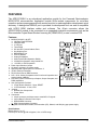
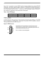
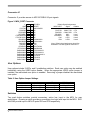
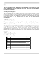
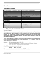
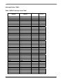
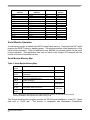
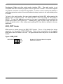
Freescale Semiconductor
User Guide
SLK0101UG
Rev. 0, 9/2006
Application Module Student Learning Kit Users
Guide featuring the Freescale MC9S12C32
For use with the following part numbers:
CSM-12C32
APS12C32SLK
PBS12C32SLK
© Freescale Semiconductor, Inc., 2006. All rights reserved.
_______________________________________________________________________
CONTENTS
CAUTIONARY NOTES ..............................................................................................................4
FEATURES ................................................................................................................................5
REFERENCES ...........................................................................................................................6
INTRODUCTION ........................................................................................................................7
GETTING STARTED..................................................................................................................7
OPERATION ..............................................................................................................................7
POWER ................................................................................................................................. 8
PWR .................................................................................................................................. 8
CONNECTOR J1............................................................................................................... 8
PWR_SEL JUMPER.......................................................................................................... 8
RESET SWITCH ................................................................................................................... 9
LOW-VOLTAGE DETECT ..................................................................................................... 9
TIMING .................................................................................................................................. 9
COMMUNICATIONS ............................................................................................................. 9
COM CONNECTOR ........................................................................................................ 10
CONNECTOR J1............................................................................................................. 11
USER OPTIONS ................................................................................................................. 11
SWITCHES ..................................................................................................................... 11
LED’S............................................................................................................................... 12
DEVELOPMENT SUPPORT ....................................................................................................12
ASCII MONITOR OPERATION ........................................................................................... 12
ASCII MONITOR MEMORY MAP ................................................................................... 12
MONITOR COMMANDS ................................................................................................. 13
INTERRUPT SUPPORT.................................................................................................. 13
INTERRUPT VECTOR TABLE........................................................................................ 14
SERIAL MONITOR OPERATION........................................................................................ 15
SERIAL MONITOR MEMORY MAP ................................................................................ 15
BDM_PORT HEADER......................................................................................................... 16
2
Freescale Semiconductor
FIGURES
Figure 1: PWR_SEL ...................................................................................................................8
Figure 2: COM Connector.........................................................................................................10
Figure 3: MCU_PORT Connector .............................................................................................11
Figure 4: BDM_PORT...............................................................................................................16
TABLES
Table 1: Serial COM Signals ....................................................................................................10
Table 2: User Option Jumper Settings......................................................................................11
Table 4: Monitor Commands ....................................................................................................13
Table 5: Monitor Memory Map..................................................................................................12
Table 6: MON12 Interrupt Vector Table....................................................................................14
Table 7: Serial Monitor Memory Map........................................................................................15
August 25, 2006
Freescale Semiconductor
A
REVISION
Initial release
3
Cautionary Notes
♦ Electrostatic Discharge (ESD) prevention measures should be used when handling this
product. ESD damage is not a warranty repair item.
♦ Axiom Manufacturing does not assume any liability arising out of the application or use of
any product or circuit described herein; neither does it convey any license under patent
rights or the rights of others.
♦ EMC Information on the APS12C32SLK module:
a) This product as shipped from the factory with associated power supplies and cables, has
been verified to meet with requirements of CE and the FCC as a CLASS B product.
b) This product is designed and intended for use as a development platform for hardware or
software in an educational or professional laboratory.
c) In a domestic environment, this product may cause radio interference in which case the
user may be required to take adequate prevention measures.
d) Attaching additional wiring to this product or modifying the products operation from the
factory default as shipped may effect its performance and cause interference with nearby
electronic equipment. If such interference is detected, suitable mitigating measures should
be taken.
TERMINOLOGY
This module uses option selection jumpers and cut-traces to setup default configuration.
Terminology for application of the option jumpers is as follows:
Jumper – a plastic shunt that connects 2 terminals electrically
Jumper on, in, or installed - jumper is installed such that 2 pins are connected together
Jumper off, out, or idle - jumper is installed on 1 pin only. It is recommended that
jumpers be idled by installing on 1 pin so they will not be lost.
Cut-Trace – a circuit trace connection between component pads. The circuit trace may
be cut using a razor knife to break the default connection. To reconnect the circuit,
simply install a suitably sized 0-ohm resistor or attach a wire across the pads.
4
Freescale Semiconductor
FEATURES
The APS12C32SLK is an educational application module for the Freescale Semiconductor
MC9S12C32 microcontroller. Application module SLK’s include components for out-of-box
operation and are preprogrammed with a serial monitor to make application development quick
and easy. A background DEBUG port is provided for development tool use and is compatible
with HCS12 BDM interface cables and software. The 40-pin connector allows the
APS12C32SLK module to be connected to an expanded evaluation environment such as the
Microcontroller Project Board Student Learning Kit (PBMCUSLK) or user’s custom PCB.
Features:
♦
♦
♦
♦
♦
♦
♦
♦
♦
♦
♦
♦
MC9S12C32 MCU, 48 QFP
♦ 32K Byte Flash EEPROM
♦ 2K Bytes RAM
♦ 31 I/O lines
♦ Timer/PWM
♦ SCI and SPI Communications Ports
♦ Key Wake-up Port
♦ BDM DEBUG Port
♦ CAN 2.0 Module
♦ Analog Comparator
♦ 8 MHz Internal Bus Operation Default
♦ 25 MHz Bus Operation using internal PLL
♦ +3.3VDC to +5VDC operation
Power Input Selection Jumper
On-board, regulated +5V power supply
Optional power input/output from Connector J1
16 MHz Ceramic Resonator
RS-232 Serial Port w/ DB9 Connector
8-Ch, 10-bit, Analog Comparator with full rail-to-rail operation and
external trigger capability
8-Channel, 16-bit Timer with Input Capture, Output Compare, and
PWM capabilities
User Components Provided
♦ 3 Push Button Switches: 2 User, RESET
♦ 3 LED Indicators: 2 User, VDD
Jumpers
♦ Disable User Components
♦ Power Select
Connectors
♦ 40 pin connector provides access to most MCU I/O signals
♦ 2.0mm Barrel Connector Power Input
♦ DEBUG BDM Connector
♦ DB9 Communications Connector
Supplied with DB9 Serial Cable, Documentation (CD), Manual, and Wall plug type power supply.
Specifications:
Module Size 2.2” x 1.6”
Power Input: +9VDC @ 200 mA typical, +6 to +16VDC range
Freescale Semiconductor
5
References
Reference documents are provided on the support CD in Acrobat Reader format.
information can be found in the Application Notes section of the Freescale Web site.
APS12C32SLKSCHEM.pdf
APS12C32SLKUG.pdf
9S12C32DGV1.pdf
9S12C32_ZIP.zip
APS12C32SLKQSUG.pdf
APS12C32SLKSW.zip
AN2548.pdf
More
APS12C32SLK Application Module Schematic
APS12C32SLK User Guide
MC9S12C32 Device User Guide
Zip file containing Device Block User Guides
Quick Start Guide for use with stand-alone module
CodeWarrior project for use with
APS12C32SLK_QSUG
Serial Monitor Program for HCS12 MCU’s
The following reference documents are for using the application module in conjunction with the
Freescale Microcontroller Project Board Student Learning Kit:
PBS12C32SLKQSUG.pdf
PBS12C32SLKSW.zip
Quick Start Guide for application module use with
PBMCUSLK
CodeWarrior project for use with
PBS12C32SLK_QSUG
Visit www.freescale.com\universityprogram for current product information, reference materials
and updates.
6
Freescale Semiconductor
INTRODUCTION
Before using this module, the user should be familiar with the hardware and software operation
of the target MCU. Refer to the MC9S12C32 User Manual and MC9S12C32 Reference
Manual for details on MCU operation. The module’s purpose is to promote the features of the
MC9S12C32 and to assist the user in quickly developing an application in a known working
environment. Users should be familiar with memory mapping, memory types, and embedded
software design for quick, successful, application development.
The APS12C32SLK Educational Module is a fully assembled, fully functional module
supporting Freescale MC9S12C32 microcontroller. The module comes with a serial cable,
power supply, and an embedded monitor for stand-alone operation. Support software for this
module is provided for Windows 95/98/NT/2000/XP operating systems.
Application development may be performed by using the embedded monitor, or any
compatible BDM cable with supporting host software. The embedded monitor provides an
effective, low cost, debug method. Note that when a BDM cable is used for debugging, the
BDM pod should be powered from an external supply.
GETTING STARTED
Please refer to the APS12C32SLK Quick Start Users Guide to quickly setup the stand-alone
application module or PBS12C32SLK Quick Start Users Guide to get started with the
microcontroller project board (PBMCUSLK).
Operation
The APS12C32SLK module provides input and output features designed to assist embedded
application development. Access to the MCU port signals is available through module
connector J1. This connector may also be used to input power to the module or to output
power to attached modules. RS-232 communications signals may also be input through
connector J1. Care must be exercised when using the J1 to power the module, as only
regulated voltage in the range of +3.3V to +5V should be supplied to this connection. The onboard regulator provides a fixed +5V voltage to the module.
Five user option jumpers and 3 cut-traces control module operation. Enabling a user option
requires installing a jumper across the associated header pins. Removing the jumper disables
the associated option. An option enabled by a cut-trace can be disabled by removing the
circuit trace between the cut-trace component pads. Use a sharp knife to cut the embedded
circuit trace. Be careful not to damage adjacent circuitry. To re-enable the option, simply
install a 1206 sized 0-ohm resistor or piece of wire across the cut-trace component pads.
Freescale Semiconductor
7
Power
Power is supplied to the module through a 2.0mm barrel connector at location PWR for standalone operation. The module may also be powered through connector J1 when connected to
the PBMCUSLK. Power may be sourced off-module through connector J1 to external circuitry.
Power routing on the module is determined by the PWR_SEL jumper.
PWR
The PWR connector accepts a 2.1mm, center-positive, barrel plug that allows the module to be
powered from a wall-plug transformer or from a desktop power supply. Input voltage should be
limited to between +7V and +20V. Input voltage of +9VDC is typical. This input supplies the
on-board +5V regulator that powers the module.
Connector J1
Power may be supplied to the module through the pins J1-1 and J1-2. Use of this option
requires a regulated voltage input limited to the range of +3.3VDC to +5VDC. This input is
connected directly to the module power and ground planes. Care should be exercised not to
over-drive this input. Use of connector J1 to supply +3.3V to the module requires disabling the
voltage supervisor (LV1) by opening cut-trace CT-1. See the Low-Voltage Detect section
below. To re-enable the low-voltage supervisor, install a 1206 sized 0-ohm resistor at CT1.
Connector J1 may also be used to source +5V power from the on-board regulator to external
modules attached to connector J1. The PWR_SEL option header determines how power is
routed to the module.
PWR_SEL Jumper
The PWR_SEL jumper is a 4-position option header that configures power routing on the
APS12C32SLK module. The module may be powered by an external transformer connected
to the PWR connector or through connector J1. The module may also source power to
auxiliary modules connected to the connector J1. Damage may occur if the J1 power input
pins are over-driven. Refer to the Figure 1 to determine correct PWR_SEL jumper setting.
Figure 1: PWR_SEL
8
1
2
Source power input from barrel connector PWR.
1
2
Source power input from connector J1.
1
2
Source power from barrel connector PWR and supply power to external
circuitry connected to J1.
Freescale Semiconductor
Reset Switch
The RESET switch provides an asynchronous reset input to the MCU. Pressing the RESET
switch produces a low-voltage level on the RESET input to the MCU. The low-voltage
supervisor (LV1) holds the RESET line low for approximately 150 ms after the pushbutton is
released.
Low-Voltage Detect
A DS1813 (LV1) provides POR, low-voltage detect, and pushbutton reset services for the
module. At power-on, LV1 holds the MCU in reset for 150 ms after VCC reaches approximately
4.35V. During normal operation, LV1 asserts RESET when VCC falls below 4.35V and holds
RESET true for 150 ms after VCC returns to normal. The push-button operation is described
in the paragraph above. Use of connector J1 to supply +3.3V to the module requires disabling
LV1.
LV1 may be disabled by opening the cut-trace CT1. Simply remove the circuit trace between
the cut-trace pads to open the circuit. To restore the circuit functionality, install a 1206 size, 0ohm, resistor or a short piece of wire across the cut-trace pads.
Timing
A ceramic resonator (Y1) provides a 16.0 MHz base operating frequency to the MCU. This
supports a default 8.0 MHz internal operating frequency. Higher frequencies are possible
using the embedded PLL. The resonator output is routed to the MCU only and is not available
at the MCU Port connector (J1). The MCU ECLK output is available to the user at connector
J1 if enabled.
Communications
The APS12C32SLK module provides a single RS-232 communications port. An RS-232
transceiver (U2) provides RS-232 signal level to TTL/CMOS logic level translation. RS232
signals TXD and RXD are routed between the transceiver and the MCU. These signals are
also routed to connector J1. RS-232 communication signals input on J1 must be TTL/CMOS
logic levels; no translation support is provided through this path. The transceiver output may
also be driven off-module if the signals are suitably buffered. As added development support,
hardware flow control signals RTS and CTS are available on the logic side of U2. These
signals are routed to vias located near the transceiver (U2). RTS has been biased properly to
support 2-wire RS-232 communications.
Freescale Semiconductor
9
Use of the J1 connector to input RS-232 signals requires disabling the on-board RS-232
transceiver. Otherwise, signal corruption may occur. Disabling the on-board transceiver is
accomplished by opening cut-traces CT1, and CT2. Simply remove the circuit trace between
the cut-trace pads to open the circuit. To restore the circuit functionality, install a 1206 size, 0ohm, resistor or a short piece of wire across the cut-trace pads.
Table 1: Serial COM Signals
COM Signal
TXD
RXD
MCU Port
PS1/TXD
PS0/RXD
Connector
J1-5
J1-7
Disable
CT5
CT4
COM Connector
A standard 9-pin D- Sub connector provides external connections for the COM port. The COM
port is configured as a DCE device. Component U2 provides RS-232 translation services.
The figure below shows the DB9 connector.
Figure 2: COM Connector
7
RTS
Female DB9 connector that interfaces to the DCE serial port via an
RS232 transceiver. It provides simple 2-wire asynchronous serial
communications without flow control. A straight-through serial cable may
be connected to a DTE device such a PC
8
CTS
Pins 1, 4, and 6 are connected together.
9
NC
1
6
TXD
2
RXD
3
4
GND
10
5
Freescale Semiconductor
Connector J1
Connector J1 provides access to APS12C32SLK I/O port signals.
Figure 3: MCU_PORT Connector
Vx
GND
PS1/TXD
PS0/RXD
PP5/KWP5
PE0/XIRQ*
PT0/PW0/IOC0
PT1/PW1/IOC1
PM4/MOSI
PM2/MISO
PM5/SCK
PM3/SS*
PE4/ELCK
PE7/XCLKS
PAD02/AN02
PAD03/AN03
PAD04/AN04
PAD05/AN05
PAD06/AN06
PAD07/AN07
1
3
5
7
9
11
13
15
17
19
21
23
25
27
29
31
33
35
37
39
2
4
6
8
10
12
14
16
18
20
22
24
26
28
30
32
34
36
38
40
PE1/IRQ*
RESET*
MODC/BKGD
NC
NC
NC
NC
NC
PAD00/AN00
PAD01/AN01
PB4
PA0
PM1/TXCAN
PM0/RXCAN
PT2/PW2/IOC2
PT3/PW3/IOC3
PT4/PW04/IOC4
PT5/IOC5
PT6/IOC6
PT7/IOC7
Default Signal Assignments
MCU PORT
Signal
Disable
PS1/TXD
PS0/RXD
PE1/IRQ*
PP5/KWP5
PA0
PB4
COM1 TXD
COM1 RXD
SW1
SW2
LED1
LED2
CT-5
CT-4
User1
User2
User3
User4
Note: Default signal assignment should be
disabled to use the signal at connector J1
User Options
User options include 2 LED’s, and 2 pushbutton switches. Each user option may be enabled
individually using the USER option header. When the appropriate USER option jumper is
installed, the associated user option is enabled. Removing a jumper disables the associated
user option.
Table 2: User Option Jumper Settings
Jumper
User 1
User 2
User 3
User 4
On
Enable SW1
Enable SW2
Enable LED1
Enable LED2
Off
Disable SW1
Disable SW2
Disable LED1
Disable LED2
MCU Signal
PE0/XIRQ*
PP5 /KWP5
PA0
PB4
Switches
Two push button switches provide momentary, active low, input to the MCU for user
applications. Pressing a switch provides a momentary low logic level input tot the MCU. SW1
and SW2 provide input to MCUI/O ports PE0 and PP5 respectively.
Freescale Semiconductor
11
LED’s
Two LED’s provide active-low, visual output for user applications. A low voltage level driven
out on the appropriate MCU port causes the LED to light. MCU ports PA0 and PB4 drive
LED1 and LED2 respectively.
Development Support
The APS12C32SLK ships from the factory with a serial monitor installed in FLASH. An ASCII
monitor is also installed to provide quick and easy debug access to the user. The text monitor
is available out of RESET. The serial monitor is available by pressing and holding SW1 as the
module exits RESET. In the discussion below, the terms text and ASCII are used
interchangeably.
ASCII Monitor Operation
The debug monitor provides a simple application development platform for developing
application code. The debug monitor allows the user to quickly and easily develop and debug
RAM based application code.
The debug monitor is accessible through the COM port using an ASCII terminal program such
as HyperTerminal or AxIDE. The terminal should be configured for 9600, 8, N, 1 with no flowcontrol. The monitor relocates the hardware interrupt vector table from 0xFF8A:0xFFFF to
0X0F8A:0x0FFF(see Table 3 below). The vectors remain in the same order as the default
hardware table. The Reset vector is reserved; user should use autostart to start applications
from reset.
ASCII Monitor Memory Map
Table 3: Monitor Memory Map
$0000 $03FF
$0800 $0DFF
$0E00 $0F8B
$0F8A $0FFF
$8000 $BFFF
$C000 $FFFF
12
Registers
1K bytes
Reserved
Internal RAM.
1.5K bytes
Monitor Reserved
Relocated Interrupt Vector Table
512 bytes
Reserved
User Program Memory
16K bytes
Protected Monitor Space
16K bytes
Freescale Semiconductor
Monitor Commands
Table 4: Monitor Commands
BF <StartAddress> <EndAddress> [<data>]
BR [<Address>]
CALL [<Address>]
GO [<Address>]
HELP
LOAD [P]
MD <StartAddress> [<EndAddress>]
MM <Address>
MW <Address>
MOVE <StartAddress> <EndAddress>
<DestAddress>
RD
OFFSET – [arg]
Proceed
RM
STOPAT <Address>
T [<count>]
Block Fill memory range with data
Set/Display user breakpoints
Call user subroutine at <Address>
Begin/continue execution of user code
Display the Mon12 command summary
Load S-Records into memory, P = Paged S2
Memory Display Bytes
Modify Memory Bytes (8 bit values)
Modify memory Words (16 bit values)
Move a block of memory
Display all CPU registers
Offset for download
Continue program execution
Modify CPU Register Contents
Trace until address
Trace <count> instructions
NOTE: Items in Italics are not implemented at this time.
Interrupt Support
All interrupt services under are provided through the relocated vector table, see Table 5 below.
Each location in the table is initialized to a value of $0000 to cause the trap of an unscheduled
interrupt. Any nonzero value will allow the interrupt to proceed to the user's service routine
that should be located at the address indicated. The interrupt service delay is +21 cycles over
the standard interrupt service.
To use vectors specified in the table, the user must insert the address of the interrupt service
routine during software initialization into the ram interrupt table. For an example, for the IRQ
vector, the following is performed:
Example:
IRQ Service routine label = IRQ_SRV
Ram Vector Table address is defined in table below, IRQ vector definition:
VIRQ EQU $0FF2 ; define ram table vector location
Place IRQ service routine address in the table:
MOVW
#IRQ_SRV,VIRQ
This vector initialization will remain in effect until a RESET is invoked.
Freescale Semiconductor
13
Interrupt Vector Table
Table 5: MON12 Interrupt Vector Table
Ram Interrupt Vector
Address
0F8A
0F8C
0F8E
0F90
0F92
0F94
0F96
0F98
0F9A
0F9C
0F9E
0FA0
0FA2
0FA4
0FA6
0FA8
0FAA
0FAC
0FAE
0FB0
0FB2
0FB4
0FB6
0FB8
0FBA
0FBC
0FBE
0FC0
0FC2
0FC4
0FC6
0FC8
0FCA
0FCC
0FCE
0FD0
0FD2
0FD4
0FD6
0FD8
0FDA
0FDC
0FDE
0FE0
0FE2
14
MCU Interrupt Vector
Address
FF8A
FF8C
FF8E
FF90
FF92
FF94
FF96
FF98
FF9A
FF9C
FF9E
FFA0
FFA2
FFA4
FFA6
FFA8
FFAA
FFAC
FFAE
FFB0
FFB2
FFB4
FFB6
FFB8
FFBA
FFBC
FFBE
FFC0
FFC2
FFC4
FFC6
FFC8
FFCA
FFCC
FFCE
FFD0
FFD2
FFD4
FFD6
FFD8
FFDA
FFDC
FFDE
FFE0
FFE2
TRAP code
02
04
06
08
0A
0C
0E
10
12
14
16
18
1A
1C
1E
20
22
24
26
28
2A
2C
2E
30
32
34
36
38
3A
3C
3E
40
42
44
46
48
4A
4C
4E
50
52
54
56
58
5A
Vector
Source
LVI
PWME
PTPI
C4TX
C4RX
C4ERR
C4WU
C3TX
C3RX
C3ERR
C3WU
C2TX
C2RX
C2ERR
C2WU
C1TX
C1RX
C1ERR
C1WU
C0TX
C0RX
C0ERR
C0WU
FEPRG
EEPRG
SPI2
SPI1
I2C
BDLC
CRGC
CRGL
PACBO
MCNT
PTHI
PTJI
ADC1
ADC0
SCI1
SCI0
SPI0
PACAI
PACAO
TOF
TC7
TC6
Freescale Semiconductor
Ram Interrupt Vector
Address
0FE6
0FE8
0FEA
0FEC
0FEE
0FF0
0FF2
0FF4
0FF6
0FF8
0FFA
0FFC
0FFE
MCU Interrupt Vector
Address
FFE6
FFE8
FFEA
FFEC
FFEE
FFF0
FFF2
FFF4
FFF6
FFF8
FFFA
FFFC
FFFE
TRAP code
5E
60
62
64
66
68
6A
6C
6E
70
72
74
76
Vector
Source
TC4
TC3
TC2
TC1
TC0
RTI
IRQ
XIRQ
SWI
TRAP
COP
CLM
RESERVED
Serial Monitor Operation
A serial binary monitor is loaded in the MCU internal flash memory. Press and hold SW1 while
pressing the RESET button or applying power. This section provides a brief description of this
serial monitor operation. Refer to application note AN2548 for complete details on the serial
monitor operation. This application note may be found on the Support CD received with the
module or from the Freescale web site.
Serial Monitor Memory Map
Table 6: Serial Monitor Memory Map
0x0000 –
0x03FF
0x3800 –
0x3FFF
0x8000 –
0xBFFF
0xC000 –
0xF77F
0xF780 –
0xF7FF
0xF800 –
0xFFFF
Registers
1K bytes
Reserved
Internal RAM
(Relocated)
Reserved
2K bytes
Fixed Flash EEPROM Block 1
(visible at RESET)
Fixed Flash EEPROM Block 2
User Vectors (Relocated)
User Reset Vector F7FE:F7FF
Vectors (Protected)
16K bytes
13.8K bytes
2.12K bytes
NOTE: Although the monitor does not support external memory, the user can enable external
memory accesses in the unfilled areas of the memory map.
The 2K-byte serial monitor program provides an RS-232 serial interface to a host PC. Serial
data rate is 115.2K bps.
The monitor is compatible with Metrowerks CodeWarrior
Freescale Semiconductor
15
Development Studio and other serial monitor interface IDE’s. The serial monitor is not
compatible with ASCII interface programs such as HyperTerm or AxIDE. The monitor supports
23 primitive commands to control the target MCU. To allow a user to specify the address of
each interrupt service routine, this monitor redirects interrupt vectors to an unprotected portion
of FLASH.
To boot to the serial monitor, the user simply pressed and holds SW1 while pressing the
RESET switch or applying power. The status of SW1 is read only during the rising edge of
RESET. To load user application on start-up, the user is responsible for programming the
pseudo-reset vector (0xF7FE:0xF7FF). Pressing SW1 after the MCU exits reset will not
access the serial monitor. After exiting reset, pressing SW1 has effect as defined in the user
application.
BDM_PORT Header
BDM access is gained through the BDM_PORT header. This is a 6-pin header that allows
connection of a compatible HCS12 BDM cable. Refer to the documentation for the specific
BDM cable used for details on its use. The figure below shows the pin-out for the DEBUG
header.
Figure 4: BDM_PORT
MODC/BKGD
16
1
3
5
2
4
6
GND
RESET*
VDD
See the HC12 Reference Manual for complete
DEBUG documentation
Freescale Semiconductor
How to Reach Us:
Home Page:
www.freescale.com
E-mail:
[email protected]
USA/Europe or Locations Not Listed:
Freescale Semiconductor
Technical Information Center, CH370
1300 N. Alma School Road
Chandler, Arizona 85224
+1-800-521-6274 or +1-480-768-2130
[email protected]
Europe, Middle East, and Africa:
Freescale Halbleiter Deutschland GmbH
Technical Information Center
Schatzbogen 7
81829 Muenchen, Germany
+44 1296 380 456 (English)
+46 8 52200080 (English)
+49 89 92103 559 (German)
+33 1 69 35 48 48 (French)
[email protected]
Japan:
Freescale Semiconductor Japan Ltd.
Headquarters
ARCO Tower 15F
1-8-1, Shimo-Meguro, Meguro-ku,
Tokyo 153-0064, Japan
0120 191014 or +81 3 5437 9125
[email protected]
Asia/Pacific:
Freescale Semiconductor Hong Kong Ltd.
Technical Information Center
2 Dai King Street
Tai Po Industrial Estate
Tai Po, N.T., Hong Kong
+800 2666 8080
[email protected]
For Literature Requests Only:
Freescale Semiconductor Literature Distribution Center
P.O. Box 5405
Denver, Colorado 80217
1-800-441-2447 or 303-675-2140
Fax: 303-675-2150
[email protected]
Design and/or Manufacturing services for this
product provided by:
Axiom Manufacturing
2813 Industrial Lane
Garland, Tx. 75041
Phone: 972-926-9303
Web: www.axman.com
Email: [email protected]
SLK0101UG
Rev. 0
09/2006
Information in this document is provided solely to enable system and
software implementers to use Freescale Semiconductor products. There are
no express or implied copyright licenses granted hereunder to design or
fabricate any integrated circuits or integrated circuits based on the
information in this document.
Freescale Semiconductor reserves the right to make changes without further
notice to any products herein. Freescale Semiconductor makes no warranty,
representation or guarantee regarding the suitability of its products for any
particular purpose, nor does Freescale Semiconductor assume any liability
arising out of the application or use of any product or circuit, and specifically
disclaims any and all liability, including without limitation consequential or
incidental damages. “Typical” parameters that may be provided in Freescale
Semiconductor data sheets and/or specifications can and do vary in different
applications and actual performance may vary over time. All operating
parameters, including “Typicals”, must be validated for each customer
application by customer’s technical experts. Freescale Semiconductor does
not convey any license under its patent rights nor the rights of others.
Freescale Semiconductor products are not designed, intended, or authorized
for use as components in systems intended for surgical implant into the
body, or other applications intended to support or sustain life, or for any
other application in which the failure of the Freescale Semiconductor product
could create a situation where personal injury or death may occur. Should
Buyer purchase or use Freescale Semiconductor products for any such
unintended or unauthorized application, Buyer shall indemnify and hold
Freescale Semiconductor and its officers, employees, subsidiaries, affiliates,
and distributors harmless against all claims, costs, damages, and expenses,
and reasonable attorney fees arising out of, directly or indirectly, any claim of
personal injury or death associated with such unintended or unauthorized
use, even if such claim alleges that Freescale Semiconductor was negligent
regarding the design or manufacture of the part.
Freescale™ and the Freescale logo are trademarks of Freescale
Semiconductor, Inc.
All other product or service names are the property of their respective
owners.
© Freescale Semiconductor, Inc. 2006. All rights reserved.