1
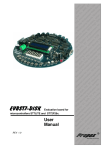
Evaluation board for
Microcontrollers, series ST7Lite1 and ST7Lite2
User’s
manual
REV 1.2
,
lu ar d ST Sta rve
a
e
,
o
Ev B VR e rs b S l
n
e
od
io , A ol
at ‘51 ntr d W inim
rr
co e
fo c ro d d s M the
e
s
d e
i
m mb o ar rs , pe C E
S
PI its n g B ro lle gh r
i
i nt H
fo
rK p
tr e to ty oco ID ers
r
F
o
rs
Pr mic s, R m m ll e
rs fo r le r gra tro
l
n
o
es ntro p r oco PC B
l
r
u o
or
c te m ic s,
f
t
m
s
s
ne Sy T stem a rd
In , S sy Bo troled PIC or ion o n b
,
es at r oc We
R
c
u
AV pr o val mic ed idd
ro E
ic ng PIC b e ds m
M n i T, m
r
ig , S s E oa e rs,
s
B
de VR Kit ng ro ll
h
t
i
r
, A rte typ on Hig
1
c
‘5 Sta oto r o ID c
P r m i R F me
rs
e
l
r s,
m rs
v e s fo lle r gra n tr l
r
Se ule tro p ro oc o
,
r
od o n s
m t c tem mic ems
i
n ne s T s t
y S y
r
he In S C , r s Bo
t
e d
PI eso tion ice
,
e R oc u a m
Sp AV op r v al IC e
r
fo icr g E T, P mb
rs s M nin , S E g
r ig
R its in
le
ol d es , AV er K typ
B `5 1 ta rt r oto roC
P for s S s P mic ,
r
r
r
rs
ds olle r we s fo o lle
r
a tr
Se ule ontr a m
n
o
d
r
b
c
c
ro We imo e t ro g o
n
p
n
e d Mi her m roc
d
t
e
d ds e st
ic
r s,
m
y
a
r
r
S T
Bo olle In , S so
e
r
d
nt ee PIC ro c sig
o
,
p
e
p
c S
o
VR cr B D Rio n
h
t
ig r A Mi
PC lua
H fo rs
,
s one solution
s
e Many ideas
a
er tro ll te m Ev ds
m n
g
s
ar
c o Sy nin Bo
1. Introduction
EVBST7-02-XXX is a development board designed for the hobbyists and engineers
who want to quickly prototype their system based on LITE1 and LITE2 family of
microcontrollers from ST Microelectronics. Developer has access to all pins of the
micro, which are brought to the header (pin connectors) and labeled accordingly.
Depending upon the board’s configuration (listed versions) some or all of the
following components are found on the board: analog thermometer, potentiometer,
relay, buzzer, RTC (real time clock) and LCD display (2x16). The pin headers
provided allow easy access to all these components. In addition, there are four
micro-switches and eight diodes which could be connected to any of the pin
connectors or additional components, which may be placed on the large, adjacent
prototype area. The power circuitry on board (bridge, voltage regulator) eliminates
the need for an external regulated power supply. This board comes with the several
examples of the C code routines (source form), to facilitate testing and quick
development in using the board’s resources.
We wish great success and full satisfaction while designing and
constructing appliances based on EVBST7-02
2
2. Board layout
1. Prototype area
2. Additional components connector
3. LED’s and micro-switches
4. Potentiometer (may be connected to the ADC of the processor)
5. LM35 thermometer
6. RESET switch and power supply LED
7. 2x16 display (optional)
8. Buzzer
9. LM317 voltage regulator
10. Power ON/OFF switch
11. Input power jack (AC/DC)
12. Relay header
13. Programmer header
14. Dual header – port A, port B
15. Programmer header
16. Standard LCD display connector
17. Socket for lithium battery
18. Real time clock M41T00 (optional)
19. Socket for processors LITE10, 15, 19, 20, 25, 29
3
3. Supported processors
ST7LITE1
ST7LITE10
FLASH
RAM(stos)
ST7LITE2
ST7LITE15
4kB
ST7LITE19
ST7LITE20
256(128)B
EEPROM
-
Peripherals
Supply voltage
Clock frequency
128B
-
-
Lite Timer with
Lite Timer with Watchdog,
Watchdog,
Autoreload Timer, SPI,
10-bit ADC with Op-Amp
Autoreload Timer
with 32-MHz clock,
SPI, 10-bit ADC with
Op-Amp
2.4V – 5.5V
To 8MHz (out OSC To 8MHz
to 16MHz
(out OSC to 1MHz)
and in 1MHz RC 1%
PLLx8/4MHz)
To 8MHz
(out OSC to 1MHz)
ST7LITE29
384(128)B
-
Lite Timer with Watchdog,
Autoreload Timer, SPI,
10-bit ADC with Op-Amp
ST7LITE25
8kB
Temperature range
Cases
256B
Lite Timer with
Watchdog,
Autoreload Timer with
32-MHz clock,
SPI, 10-bit ADC with
Op-Amp
To 8MHz (out OSC to
16MHz
and in 1MHz RC 1%
PLLx8/4MHz)
from -40ºC to 85ºC
SO20 300”, DIP20
4. Power supply for board
Recommended external power supply voltage is 7-12V AC, or 9-15V DC. A standard
power jack (bolt diameter 2.1mm - negative) is provided at the edge of the board.
Stabilized voltage Vdd is available on the double header and on the prototype area of
the board. The selection of the Vdd is provided through a 3V3 header. The default
voltage Vdd is 5VDC (no jumper on 3V3 header). By placing a jumper Vdd becomes
3.3 VDC. The SUPPLY header allows for direct access to the power jack input.
Placing a jumper bypasses the bridge and voltage regulator.
5. Peripheral circuits
5.1. LED’s
The board has 8 LED diodes, which make the simplest interface between the system
and the user. This is especially useful for the beginners, who want to manipulate or
debug their program with different hardware configurations. The diode turns on after
grounding of the associated LDn (n = 0 – 8) pin.
V dd
R
1k
LDn
L ED
L Dn
L D1
L D2
L D3
L D4
4
5.2. Switches
The board is equipped with 4 micro-switches. Pressing one of them causes
grounding of the corresponding pin on the KEY header.
V dd
R
1 0k
S Wn
Sn
SW
K EY
G ND
S W1
S W2
S W3
S W4
5.3. Relay
Access to the relay circuitry consists of the REL pin of the MISC header and pins:
NC, NO, COM of the relay header. REL pin is indirectly connected to the base of the
transistor. Logic level 1 (5 or 3.3 VDC) applied to the REL pin, will activate the relay.
External circuits can be controlled via NC, NO, COM I/O pins.
Vdd
R
Q
BC 85 7
4 k7
REL
COM
NO
RL1
RELAY
NC
D
GND
5.4. Acoustic indicator
The board has an acoustic indicator turned on and off by the transistor. The base of
the transistor is connected to the SPK pin of the MISC header. Logic level ‘1’ (5 or
3.3 VDC) applied to the SPK pin, will activate the buzzer.
Vdd
Q2
BC 557
R8
4k7
SPK
SPK
BUZER
GND
5
5.5. Thermometer
The board has one temperature sensor LM35. This voltage on output (Vout) is
proportional to the gradient of the ambient temperature. Access to Vout is provided
by LM35 pin of the MISC connector. User can wire this pin to the micro’s A/D input
and manipulate temperature measurements
GND
Vout
3
2
1
VCC
U3
LM35
Vdd
GND
R9
75
C9
1u
LM35
GND
5.6. Potentiometer
The board is equipped with one potentiometer, allowing for simulation of the analog
circuit outputs. The potentiometer enables the adjustment of voltage in the range
0-Vdd. The potentiometer output is accessible on ADJ pin of the MISC connector.
Vdd
ADJ
R10
POT1
GND
5.7. Interface RS232
There is a DB-9 connector on the board, connected with the ST3232 state converter.
On the other side of the converter there are pin connectors with converter circuit
terminals, allowing to plug in to the processor.
5.8. Real time clock M41T00
The board has one real time clock with battery back-up. The clock communicates
with the micro through the I2C interface. All the connections needed for controlling the
M41T00 circuit are brought out to the RTC pin header. The battery pin is also placed
on the header.
5.9. LCD display
The board has one LCD display interface. The LCD connector has four data lines
and two control lines: strobe line E and control line R/S. The display R/W line is
permanently connected to ground; all other lines are available at the pin header. The
adjustment of contrast is done by the selection of the resistors in the bridge circuit.
6
6. Headers and connectors
6.1. Peripherals
PA0...PA7 – processor port A
PB0...PB4 – processor port B
RST – reset
GND – ground
Vdd – voltage supply
RxD, TxD – converter ends RS232
BAT – battery
SDA – I2C real time clock interface data line
SCL – I2C real time clock interface clock line
FT – real time clock operation correction line
REL – relay
POT – potentiometer
LM35 – thermometer
BUZ – speaker
LD1...LD4 – diodes
SW1...SW4 – micro-switches
6.2. LCD display
D4...D7 – LCD data lines
RS – control line LCD data/order
E – strobe line LCD
PA0...PA5 – microcontroller port A lines
6.3. Relay
NO – normally open
NC – normally closed
COM – common
7
6.4. Programmer's connector
CLKIN –optional external clock closed with the CLK jumper
Vdd – voltage supply
GND – ground
RESET –reset
ICCLK –clock
ICDATA –data
7. Jumpers, supply LED and reset
3V3/5V – jumper shorted power is 3.3V, open 5V.
SUPPLY – shorted regulated voltage is provided from local power circuitry, open
voltage comes from the external power supply
CLK1, SWC1 – allow to choose the source of the processor'
s clock signal. When it is
quartz-controlled, both jumpers should be disconnected. When it is
controlled by internal RC circuit, both jumpers should be connected to
ground. Shorted allows for the external clock to the processor ex.
from the programmer. In that case SWC1 jumper should be closed,
and CLK1 jumper:
A – clock signal is connected from programmer’s connector to PB4
B – signal is connected from programmer’s connector to OSC1/CLK
input
C – internal RC circuit is chosen
Vdd LED – power LED indicator
RST – pressing this button causes hardware reset
8. Demo programs
LCD.c displays scrolling "EVBST7-01-XXX" string on the LCD panel
LED_ADC.c potentiometer setting is displayed by a pattern of the LED diodes
TERMOMETR.c measured temperature in [oC] is displayed on the LCD panel
RTC.c displays the current date in the form: hour : min : day : month : year.
The update of the clock settings using the keyboard. Microcontroller'
s port
lines should be connected with the appropriate lines SDL and SCL in circuit
M41T00 connected to the pin connectors.
RS.c program RS 232, the program uses external interrupts and those from
the timer, the TxD and RxD lines should be connected to the corresponding
terminals of the ST3232 circuit, brought out to the pin connectors.
LED.c pressing one of the switches turns on a pattern of LED lights
8
9. Available versions
The set System EVBST7-02 Advance includes:
EVBST7-02 board, which includes: ST7Lite29 processor, all connectors,
diodes, switches, transmitter, buzzer, thermometer, potentiometer, batterybacked RTC, converter RS with RS connector, LCD socket.
Cables to connect peripheral devices (optional)
LCD (optional)
CD-ROM with manuals and software
The price list is available on our web page: www.propox.com
9
10. Schematic diagram
RT C (Optional)
RELAY
GND
B AT
FT
SC L
SDA
Q2
B C 8 57
R EL1
4k 7
Q1
R 10
B C 5 57
4k 7
B UZ1
R 23
4. 7k
R 21
4. 7k
D1
R 20
4. 7k
Vdd
R L1
R ELAY
JP 10
REL 3
REL 2
GND
LCD (Optional)
B UZ1
POT
R ST
U3
PA5
PA4
PA3
PA2
PA1
PA0
PB 4
LC D
1
3
PA6
R 25
Vdd
PB5
PB6
PA7
R 26
4. 7k
IC CLK
PA4
PA3
PB 2/ MIS0/ AIN2
PB 3/ MOSI/ AIN3
PB 4/ CLKIN/AIN4
PB 5/ AIN5
PB 6/ AIN6
PA7
PA6/ MC O/ ICC CLK/ BR EAK
PA5/ ATPWM3 /IC CDATA
PA4/ ATPWM2
PA3/ ATPWM1
R 28
4. 7k
GND
SWITCH
+
R 16
10 k
R 15
10 k
K2
K3
K4
S0
S1
S2
S3
C 12
Vdd
10 0n
C 13
10 0n
1
2
3
4
5
6
7
8
C 1+
V+
C 1C 2+
C 2VT2 ou t
R 2in
+
GND
R7
1k
R6
1k
R5
1k
Vdd
R4
1k
Vdd
R3
1k
1
3
L4
L3
L8
L6
GND
1
3
5
7
K3
K1
2
4
6
8
L2
L1
L7
L5
R S 2 32C
GND
1
3
5
7
9
Vdd
PB 4_ 1
SUPPLY
2
4
6
8
10
IC DATA
IC CLK
R ESET
IC P
GND
C3
47 u
C6
10 0n
R 22
24 0
OUT
A DJ
+
R 11
1k
IN
3
C4
10 0n
GND
GND
R 19
82 0
+
C7
47 u
B1
GND 4
R EL4
R EL2
R EL3
3
R 17
39
B RIDGE1
3
2
1
1
2
3
R EL
JP _S
VCC _IN
2
Vdd
2
4
LED
Vdd
R2
1k
Vdd
GND
R ESET
PA0
PA1
PA2
PA3
PA4
PA5
PA6
PINS
1
6
2
7
3
8
4
9
5
Tx D
R xD
1
Vdd
2
4
6
8
10
12
14
16
18
20
C 10
10 0n
ST32 32
2
Vdd
1
3
5
7
9
11
13
15
17
19
KEY
GND
LM3 17
Vdd
SUPPLY
Vdd
GND
C8
20 p
SWC 1
GND
LEDS
Vdd
Y2
16 MHz
16
15
14
13
12
11
10
9
VCC
GND
T1 ou t
R 1in
R1ou t
T1 in
T2 in
R2ou t
GND
GND
C LKIN
PB 0
PB 1
PB 2
PB 3
PB 4
PB 5
PB 6
PA7
PA7
GND
GND
U4
+
K1
10 0n
C1
K4
K2
RS232
+
R 12
10 k
GND
GND
PA0
PA1
PA2
R EL1
TEM
GND
C 11
10 0n
Vdd
10 0n
C 14
R 13
10 k
20 p
C9
C LKIN
GND
Vdd
PB 1
PB 0
R ESET
Vdd
GND
ST7LITE10
ST7LITE15
ST7LITE19
ST7LITE20
ST7LITE25
ST7LITE29
IC DATA
Vdd
20
19
18
17
16
15
14
13
12
11
SC K/AIN1/ PB 1
SS/AIN0 /PB 0
R ESET
Vdd
Vss
C LKIN/OSC 1
OSC 2
LTIC /PA0
ATIC /PA1
ATPWM0/P A2
2
4
1
Vdd
GND
1
2
3
4
5
6
7
8
9
10
PB2
PB3
+
GND
11
9
7
5
3
1
FT
SC L
MISC
JP 9
12
10
8
6
4
2
2
4
POT
GND
C LKIN
PA5
R8
1k
1
3
R TC
R ESET
R 24
68 0
R9
1k
TEM
PB 4_ 1
7. 5k
Vdd
B AT
SDA
75
C2
1u
MCU
C LK1
GND
LC D 2X16
(o pti onal)
Vdd
1
2
R S23 2
GND
B UZ1
B UZER
GND
R xD
Tx D
GND
R 14
Vdd
Vdd
R1
ADJ
GND
GND
D7
D6
D5
D4
D3
D2
D1
D0
E
R /W
R /S
KONTR
Vcc
GND
CONNECTORS
R EL4
R TC _M41T00
B T1
3V C R2 03 2
16
15
14
13
12
11
10
9
8
7
6
5
4
3
2
1
G ND
R 27
Vdd
V ou t
8
7
6
5
Vcc
FT/OUT
SC L
SDA
V CC
OSCI
OSCO
Vbat
Vss
RES. ADJ.
Vdd
1
1
2
3
4
U1 TEMP
LM3 5
2
U2
Y1
32 .7 68k Hz
BUZZER
Vdd
Vdd
GND
3
C5
10 0n
LD0
LD1
LD2
LD3
LD4
LD5
LD6
LD7
GND
GND
http://www.propox.com
R 18
68 0
L8
L7
L6
L5
L4
L3
L2
L1
3V3/ 5V
Error : Logo FINAL_man y2 .bmp file not fo und .
Title: EVBST 7-02-XXX
Size:
GND
10
Rev:
File:
Date: 27-04-2004
GND
Sheet 1 of 1
1.00