1
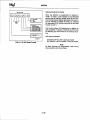
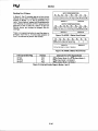
AD1000User'sManual
ffi
RearTimeDevices,
Inc.
" Accessin
g theAnalogWorld".,
ISO9001 and AS9100 Certified
^nla\a\/l
User'sManual
ffi
INC.
REALTIMEDEVICES,
Drive
820NorthUniversity
PostOfficeBox906
16804
StateCollege,Pennsylvania
Phone:(814)234-8087
FAX:(814)234-5218
Publishedby
RealTimeDevices,Inc.
820N. UniversityDr.
P.O.Box 906
StateCollege,PA 16804
Copyright@ 1993by RealTimeDevices,Inc.
All righs reserved
Printedin U.S.A.
TABLE OF CONTENTS
INTRODUCTTON......
.............t-l
Application Software
CHAPTER 1 - BOARD SETTINGS
1-l
Factor-Con
n.P3,andP4
...........14
(EOC)Interrupt(FactorySeuing:Disabled)
n. * AIDEnd-of-Convert
....'......14
P3 -8254 Timer/CounterOutputInterrupt(FactorySetting:Disabled)
..................1'5
P4 - EXTINT andPPI PC3Intemrpts(FactorySetting:Disabled)
P5 _ 8254Timer/CounterI/O HeaderConnector(FactorySettings:As Shownin Figure1-5)......................1'5
..............1-8
P6- BaseAddress(FactorySetting:300hex(768decimal) .................
........................1-9
Monitor(FactorySetting:8255PPIPortB, Bit 7) ."........
P8- End-of-Convert
CHAPTER 2 _ BOARD INSTALLATION
Connecting
andDiginl I/O ...............
theTimer/Counters
Connecting
Program
Diagnostics
RTDDIAG
Runningthe
CHAPTER 3 -
HARDWARE DESCRIPTION ...........
Interface
Peripheral
DigitalI/O, Progammable
CHAPTER 4 BA + 0:
BA + l:
BA + 2:
BA + 3:
BA + 4:
BA + 5:
BA + 6:
BA + 7:
BA + 8:
BA + 9:
BOARD OPERATION AND PROGRAMMING
ChannelI (AINI) Select(WriteOnly)..........
Channel2(AIN2)Select(WriteOnly)..........
Channel3 (AIN3) Select(WriteOnly) ..........
Channel4(AIN4)Select(WriteOnly)..........
Channel5(AIN5)Select(WriteOnly)..........
Channel
6 (AIN6)Select(WriteOnly)..........
Channcl7 (AIN7)Select(WriteOnly)..........
S (AIN8)Select(WriteOnly)..........
Channel
...........'.
MSB Data(Read/IVrite)
Start12-BitConvcrsion/Read
.............
LSB Dara@eadAMrite)
Start8-Bit Conversion/Read
............2-1
......-...........24
............-..-.-.24
..-..-.--.-.-3-1
.................34
..........-.4.1
......................4-3
---.-........-........4-3
......................4-3
......................44
......................44
......................44
......---.............44
.....................'44
..............44
-.....---.-......44
BA +
BA +
BA +
BA +
BA +
BA+
BA +
BA +
................
12: PPIPortA - DigitalI/O (ReadlTVrite)
.............
13: PPIPortB - DigitalI/O (ReadAilrite)
14:PPIPorrC - DigitalI/O (Read/write).............
15: 8255PPIControlWord (WriteOnly)...........
.................
0 (ReadAMrite)
16: 8254Timer/Counter
I (Read/IVrite).................
l7: S254TimerlCounter
2 (Read/lVrite)
18: S254TimerlCounter
ConnolWord(WriteOnly) ...........
19: 8254Timer/Counter
.............44
................4-5
.,...............4-5
.....................4-5
...-.......-.....4'6
.........-.......4'6
.............4-6
....................-...46
..................4-8
.........................4-9
.....4-9
Startingan AID Conversion
MonitoringConversion
Status..........
Data............
ReadingtheConverted
What Is
IntenuptController
8259Programmable
IntemrptMaskRegister(IlvR) ..........
End-of-Intemrpt(EOI) Command
WhenanIntemrptOccurs?
WhatExactlyHappens
UsingIntemrptsin Your Programs
for ADl000IntenuptProgramming
SpecialConsiderations
Writingan IntemrptServibeRoutine(ISR)
Savingthe StartupInterruptMaskRegister(IMR) andInterruptVector
Restoringthe StartupIMR andInterruptVector
CommonIntemrptMislakes
.................4-10
......4-10
......4-10
.....................4-10
.....4'll
.......4-11
.............4-ll
.,......-.4'12
.-..-4'13
.......-.......4-13
......4-15
Examplehograms andFlow Diagrams
SingleConvertFlow Diagram(Figure4-3).............
.....................4-16
CHAPTER5 - CALIBRATION
SPECIFICATIONS
APPENDIX A _ AD1OOO
APPENDIX B - CONNECTORPIN ASSIGNMENTS
A-1
APPENDIX C - COMPONENT DATA SHEETS
FOR SIGNAL*MATH..........
APPENDIX D _ CONFIGURING THE AD1OOO
c.t
FOR ATLANTIS
APPENDIX E_ CONFIGURING THE AD1OOO
APPENDIX F - WARRANTY
I,I
B-l
..........D.I
.E-l
F-1
LIST OF ILLUSTRATIONS
1-1
t-2
1-3
t4
1-5
1-6
t-7
1-8
2-l
2-2
3-l
4-l
4-2
4-3
5-1
Settings...................
BoardLayoutShowingFactory-Configured
InteruptChannelSelection
Jumper,P2 ................
End-of-Convert
Interrupt
P3
Output
Jumpers,
8254Timer/Counter
P4
EXTINT andPC3InterruptJumpers,
P5 ............
Timer
Interval
Jumpers,
8254Programmable
8254andP5Circuitry
P6................
BaseAddress
Jumper,
End-of-Convert
Jumper,P8 ................
Assignments
.................
Yl ltO ConnectorPin
AnalogInputConnection
..............
AD1000BlockDiagram.................
TimingDiagram
A,/DConversion
Circuiry
S?S4TimerlCounter
Flow Diagram
SingleConversion
iii
..................
l'3
...............1-4
...................1-5
..............1-5
..........1-6
......................1-7
l-8
......................
..................1-9
.....2-3
........................24
......................3-3
........................4-8
.......4-14
.......................4'16
iv
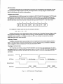
INTRODUCTION
i-1
The AD1000mediumspeedmultichannelanaloginputboardturnsyoru IBM PCIKT/AT or compatible
dataacquisitionandcontrolsystem.Installedwithin a singleshortor full-size
computerinto a high-performance
expansionslot in thecomputer,the ADl000 boardfeatures:
. Eight single-ended
analoginputchannels,
. l2-bit,20 microsecond
A/D converter,
. 25 l<7lzmaximumthroughput,
. +5 volt analoginputrange,
. Threeindependent
8-MlIz timer/counters,
. 24TILICMOS-compatible8255-based
digitalI/O lines(16 at theVO connectorand8 at on-boardpads).
The following paragraphs
briefly describethemajorfunctionsof theboard.More detaileddiscussions
of board
functionsareincludedin Chapter3, HardwareDescription,andChapter4, Board OperationandProgramming.The
boardsetupis describedin Chapterl,Board Settings.
Analog-to-DigitalConversion
The analog-todigital(A/D) circuitryreceivesup to eightsingle-ended
analoginpus andconvertstheseinputs
into l2-bit digital datawordswhich canthenbe readand/ortransferred
to PC memory.
The input voltagerangeis -5 to +5 volts,with overvoltageprotectionto +35 volts.A/D conversions
areperformedby an industrystandard12-bit successive
approximation
converter.This high-performance
converterand
amplifierprecedingit makesurethatdynamicinput voltagesareaccurately
thehigh-speedsample-and-hold
digitized.Theresolutionof a 12-bitconversionis2.4414millivolts andthemaximumthroughputis 25 kIIz.
The converteddatais readand/ortransferredto PC memory,onebyte at a time, throughttrePC databus.
8254Timer/Counter
An 8254programmable
intervaltimer containsthree16-bit,8-MHz timer&ountersto supporta wide rangeof
timing andcountingfunctions.The clock,gateandoutputpinsfor eachof the threetimer/counters
areavailableat
the I/O connector.
Digital VO
TheADl000has24TlLlCMOS-compatible
digitalVOlineswhichcanbedirectly
interfaced
withextemal
devicesor signalsto senseswitchclosures,triggerdigital evens,or activatesolid-staterelays.The linesarcproperipheralinterface@PI)chip. Sixteenof the linesarebroughtout to fie
videdby theon-board8255programmable
VO connectorandeightareavailableat a setof on-boardpads.
What ComesWith Your Board
You receivethe following itemsin your ADl000 package:
. AD1000interfaceboard
. Softwareanddiagnosticsdiskettewith exampleprognmsin BASIC, TurboPascal,andTurboC; sourcecode
. Ljser'smanual
pleasecall RealTime Devices'CustomerServiceDepartmentat
If any item is missingor damaged,
(814)234-8087.If you requireserviceoutsidetheU.S.,contactyour local distributor.
Board Accessories
In additionto theitemsincludedin your AD1000package,RealTime Devicesoffersa full line of softwareand
Call your local distributoror our mainoffice for moreinformationabouttheseaccessories
hardwareaccessories.
and
for helpin choosingthebestitemsto supportyourboard'sapplication.
i-3
Application Softwareand Drivers
provideexcellentdataacquisitionandanalysissupport.Use
Our customapplicationsoftwarepackages
digital signalprocessingandanalysis,or
SIGNAL*MATH for integrateddataacquisitionandsophisticated
ATLANTIS for real-timemonioring anddataacquisition.rtdlinx andrtdlinxA.{B driversprovidefull-featured
high level interfacesbetweenttreAD1000andcustomor third partysoftware,includingLabtechNotebook,NotebooktG,, andLT/Conuol.rtdlinx sourcecodeis availablefor a one-timefee.Our PascalandC Programmer's
sourcecodefor customprogpmming.
Toolkit providesroutineswith documented
Hardware Accessories
Hardwareaccessories
for the AD1000 includetheTB40 terminalboardand XB40 prototype/terminalboardfor
prototypedevelopment
andeasysignalaccess,EX-XT andEX-AT extenderboardsfor simplifredtestingand
debuggingof prototypecircuitry,andthe XP40singlewire flat ribboncablefor externalinterfacing.The AD1000
canbe interfacedto RTD's 50-pinchannelexpansionandsignalconditioningboardsby usinga DiscreteWire Kit
UsingThis Manual
This manualis intendedo helpyou installyour newboardandget it runningquickly,while alsoproviding
enoughdetailabouttheboardandits functionsso thatyou canenjoymaximumuseof its featuresevenin themost
of dataacquisitionprinciplesandthatyou
complexapplications.We assumethatyou alreadyhavean understanding
programs.
cancustomizetheexamplesoftwareor write yourown applications
When You NeedHelp
This manualandtheexampleprogramsin thesoftwarepackageincludedwith your boardprovideenough
informationto properlyuseall of theboard'sfeatures.If you haveanyproblemsinstallingor usingthisboard,
(814)234-8087,duringregularbusinesshours,easternsandardtime u
contactour TechnicalSupportDepartment,
qrtern daylighttime,or senda FAX requestingassistance
to (814)234-5218.Whensendinga FAX request,please
includeyour company'snameandaddress,your name,your telephonenumber,anda brief descriptionof the
problem.
i-4
CHAPTER1
BOARD SETTINGS
TheAD1000boardhasjumpersettingsyou canchangeif
as
necessary
for your application.The boardis factory-configured
listedon the tableandshownin thediagramat the beginningof
this chapter.Shouldyou needto changethesesettings,usethese
easy-to-followinstructionsbeforeyou installthe boardin your
computer.
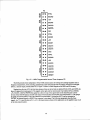
1-1
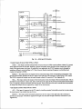
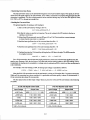
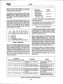
Factory-ConfiguredJumper Settings
jumperson theADl000 board.Figure 1-1showsthe
Table1-1liss thefactorysettingsof theuser-configurable
explainhow to changethe
boardlayoutandthe locationsof thefactory-setjumpers.Thefollowingparagraphs
facory settings.Payspecialattentionto the settingof P6, ttrebaseaddressheaderconnector,to avoid address
contentionwhenyou first useyour boardin your system.
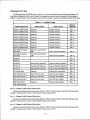
Table1-1- FactorySettlngs
Jumper
FunctlonControlled
FactorySettlng
P2
theA/Dendof-convert
Connects
signalto an interrupt
channel
Disabled(notconnected)
P3
oneof lhe 8254timer/counter
Connects
outputsto an
channel
interrupt
P4
Conneclsan externalinterrupt
or an interrupt
generated
by the PPI(INTRA)to an interrupt
channel Disabled(nolconnected)
Disabled(notconnected)
P5
Configuresthe 8254timer/counters
Alltimer/counters
are
cascaded
(seediagramfor P5)
P6
Setsthe baseaddress
300 hex(768decimal)
P8
theA/Dendofconvertsignalsothatit can
Connects
lhroughlhe PPIat PA7,PB7,or PQ7
be monitored
throughPB7
Monitored
P9
for soldering
8255PortB padsavailable
connsctions Noconnections
o
o
o
o
o
o
o
o
o
o
o
o
o
o
o
o
o
o
o
o
o
o
o
o
UI
o
o
o
o
o
o
o
o
o
o
o
o
o
o
@
Fg
Esl
ooooooooooooo
[,t deint sA
al
Real Time Dovbos, lm. State Collego,PA 16804 USA
At
pr
Fig.1-1- BoardLayoutShowingFactory-Configured
Settings
1-3
@
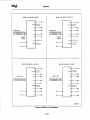
P2, P3, and P4 - Interrupts
HeaderconnectorsP2, P3, andP4 let you connectvariouson-boardand externalsignalsto the computer's
by theA/D converter'send-of-convert
signal,by any oneof thetfuee
intemrptchannels.Intemrptscanbe generated
peripheralinterfaceor from an externalinterruptsource
timer/counteroulputs,andby the 8255programmable
broughtonlo theboardthroughthe VO connector.
Beforetrying to useinterrupts,you mustbe familiar with theprocedurefor initializingthe intemrptvectorsand
arebeyondthescope
thePC's intemrptcontroller,andsettingup $reintenupthandlingroutines.Theseprocedures
to effectivelyuseint€rruptsin your computersystem.Chapter4 providesan
of this manual,but mustbe understood
overviewon usingintemrpts.
Also, be carefulto avoidcontentionwith otherdevicesthatmay useintemrptsin your computerwhenyou
chooseyour intemrpt channel.Eachinterruptsourceactivatedmustbe assignedto an unusedintemrpt channel.Use
the table insidethe back coverof this manual!o recordthe interruptchannelyou haveselected.
It is also very importantto note that the boardinternrptsourceis a TTL totem-pole(pustr&ull) type output; it is
not open-collector.Therefore,do not connectthis intenupt to any otherintemrpt output!
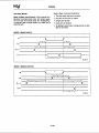
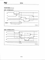
.P2 - A/D End-of-Convert(EOC)Interrupt @actorySetting:Disabled)
(EOC)signalto
HeaderconnectorP2, shownin Figurel-2, letsyou connecttheAID converter'send-of-convert
(lowest
priority
(highest
priority
IRQT
channel).
through
intemrpt
IRQ2
channel)
channels,
any of thecomputer's
jumper
jumper
placing
pins,
in
Figure
l-Za.By
leftmost
this
is
vertically
two
shown
The
stored
acrossthe top
as
generate
pins
Figure
be
used
to
intemrps.
IRQ
channels,
EOC
can
horizontally acrossthe
of oneof the
the
signal
goes
is
intercompleted;
therefore,
an
IRQ3.
EOC
high
when
1-2bshowsthe EOC connectedto
The
a conversion
(not
(converting)
converting).
EOC
line
from
low
high
rupt will occurwhenthe
transitions
to
IRQT
IRQT
IRQ6
IRQ6
IRQ5
rRos
IRQ4
IRQ4
IRQ3
IRQ3
IRQ2
IRQ2
Fig.1-2b:EOC
to 1RQ3
connected
Fig.1-2a:Factory
setting(disabled)
Fig. 1-2 -
End-of-ConvertInterruptChannelSelectionJumper, P2
. P3 - E254Timer/CounterOutput Interrupt (FactorySetting:Disabled)
HeaderconnectorP3, shownin Figure l-3, is usedto jumperoneof thethree8254timer/counteroutputs,
OUT0, OLJ"TI,or OUTZ,to oneof thecomputer'sinterruptchannels,IRQ2 (highestpriority channel)throughIRQT
(lowestpriority channel).The top six pairsof pins on this headerconnectorareusedto selectthe IRQ channel,and
thebottomthreepairsof pins areusedto selectthe desired8254output.The two jumpersstoredverticallyacrossthe
top four pairsof pins,asshownin Figure I -3a,mustbe installedto connectan 8254outputto an intemrptchannel.
Placeonejumperhorizontallyacrossthepins of theselectedtimer/counteroutput(oneof thebottomthreepairsof
pins).Thenplacethe secondjumperacrossthepins of theselectedintemrptchannel(oneof thetop six pairsof
pins).Figure1-3bshowsan example.
t4
IRQT
IRQT
IRQ6
IRQ6
IRQs
IRQ5
IRQ4
IRQ4
IRQ3
IRQ3
IRQ2
IRQ2
OUTO
OUTO
OUTl
OUTl
OUT2
OUT2
Fig.1-3b:OUT2
to lRQ4
connected
Fig.1-3a:Factory
settings(disabled)
Fig. 1-3 -8254 Timer/Counter
OutputInterruptJumpers,P3
. P4 - EXTINT and PPI PC3Interrupts (FactorySetting:Disabled)
HeaderconnectorP4, shownin Figure 14, letsyou connectan externalsignal,EXTINT, or the 8255PPI'sPC3
(tr {TRA) signalto oneof thecomputer'sinterruptchannels,IRQ2 (highestpriority channel)throughIRQT(lowest
whenthe
priority channel).EXTINT is routedontotheboardthroughexternalI/O connectorF7. PC3is generated
8255PPI is beingoperatedin modeI or mode2, asexplainedin thedatasheetin AppendixC. To connectoneof
thesetwo signalsto an interruptchhnnel,thetwo storedjumpers,shownin Figurel-4a, mustbe installedacrossthe
appropriatepairsof pins. Placeonejumperhorizontallyacrossthepinsof thesignalchosenandplacethe second
jumperhorizontallyacrossthepins of theselectedIRQ channel.Figurel-4b showsthePC3connected0oIRQ7.
IRQT
IRQT
IRQ6
IRQ6
IRQ5
IRQ5
!RQ4
IRQ4
tR03
IRQ3
IRQ2
IRQ2
PC3
PC3
EXTINT
EXTINT
Fig.1-4b:PC3
to |RQT
connected
Fig.1-4a:Factory
settings(disabled)
Fig. 1-4 -
EXTINTand PC3 InterruptJumpers,P4
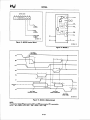
PS -8254 Timer/CounterVO HeaderConnector(FactorySettings:As Shownin Figure 1-5)
intervaltimer's clock andgate
HeaderconnectorP5, shownin Figure l-5, configuresthe 8254programmable
Also includedon P5 arepins to routean externalintenupt(EXTIIVD from andthe
sourcesandoutputconnections.
computer'sRESETsignalto extemalI/O connectorP7.Figurel-5 showsthe factorysettings.All threetimer/
Thesearethe settingsusedby SIGNAL*MATH andATLANTIS acquisitionandanalysis
countersarecascaded.
software(seeAppendixesD andE).
l-5
;l
H
XTAL
OO
EXCKO
H
+5V
OO
EXGTO
H
CKOTO
oo
CKOTO
H
cKl
xl
XTAL
H
EI
+5V
OO
EXGTl
H
CKOTl
oo
CKOTl
H
cK2
oa
XTAL
OO
EXCK2
H
+5V
oa
oo
EXCKl
5l
;l
8lo o
EXGT2
H
CKOT2
OO
CKOT2
O'
EXTINT
aa
RESET
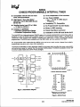
Fig. 1-5 -8254 ProgrammablelnlervalTimer Jumpers,P5
The 8254 providesttrreeindependentl6bit, 8 MHz timer/countersfor timing and countingfunctionssuchas
eventcounting,andintemrps.Eachtimer/counterhastwo inputs,clock (CK) in andgate
frequencymeasurement,
(GT) in, andoneoutput,timer/counterOUT. Figure 1-6showsa blockdiagramof the8254andP5 circuitry.
Srartingfrom thetop of P5, thefint threegroupsof pinson the left sidearelabeledCLK0, GT0, andOUTO,the
threeI/O signalsfor timer/counter0. The signalson theright sidefor timer/counter0 arelabeledXTAL, EXCK0,
+5V, EXGT0, CKOTO,CKOTO(this signalhasa bar overtop of thesignalnameon theboardbecauseit is the
timer/counter0 to timer/counter1). The goups
inverseof theCKOT0 signal),andCKI (theoutputwhichcascades
of signalsfor timer/countersI and? ue identicalo timer/counter0, exceptthat OUT2 canbe connectedto
describethese
EXTINT, an externalsignal,or RESET,thecomputer'sresetsignal.The following paragraphs
be
appliedto any or all
the
application
can
place
names
whenever
of 0, 1, or 2 in the signal
signals.An "x" is usedin
of the threetimer/counters.
t-6
82s4PtT
TIMER/
COUNTER CLK
0
GATE
CLKOUTO/CLKOUTO.
OUT
^!
TIiIEF/
COUNTEF
sMHz
il,ttot,
CLK
;-''l- *u
I
GATE
I
,,".rj ExrcLKl
cLKourr !
OUT
TIMER/
COUNTER CLK
2
GATE
cLKour2- .l
OUT
CLKOUTz/CLKOUT2.
(EXTINT/FESET)
to to
Ea^M
PCBUS
z
RESET
.^
I
Fig. 1-6 -8254 and P5 Circuitry
. CounterInputs (ConnectOnly ONE at a Time):
circuitsis from the5 MHz crystaloscillator,labeledYl, located
XTAL - This input o all ttrreetimer/counter
jumper
horizontallyacrossthepair of pinsconnectsthe 5 MHz
in the upperleft cornerof theboard.Installinga
your
application,the XTAL frequencycanbe changedby
clock to the timer/counterclock input. If requiredby
installinga differentcrystaloscillaor at Yl. Note,however,thatthemaximumfrequencyat which thetimer/
counterswill operateis 8 MHz.
EXCKX - This input allows an extemalclock to control the timing of the correspondingtimer/counter.This
pin mn be horizontallyjumperedto the CKx input on ttreright sideof the connector,in placeof the XTAL source.
The EXCKx signalsarebroughtonto the board throughextemalI/O connectorP7 (seeAppendix B).
CKx is
to theclock input of the next timer/counter.
CKx - This input connectsthe outputof onetimer/counter
providedfor timer/counters
I and2 only, andis connectedto theoutputof theprevioustimer/counter(timer/counter
areusedto cascadethetimer/counters
0 or 1) by placinga jumperhorizontallybetweenthepins.Theseconnections
for longertime delaysthanaresupportedby a singlel6-bit timer/counter.
. GateInputs (ConnectOnly ONE at a Time):
+5V - This input,if connectedto theGTx inputby installinga jumperhorizontallyacrossthetwo pins,places
the timerhounter in an enabledstateat all times.
EXGTx - This input canbe horizontallyjumperedto tre GTx input on theright sideof theconnectorto
providean extemalgate.The EXGTx signalsarebroughtonto theboardthroughextemalI/O connectorP7 (see
AppendixB).
t-7
. CounterOutputs(ConnectOnly ONE at a Time):
CKOTx - This oulput canbe horizontallyjumperedto the correspondingOUT pin on the right sideof the
connectorso that the timer/counter'soutput signalcanbe routedto externalVO connectorP7 (seeAppendix B). The
CKOTx signalsareavailableat P7.
OUT pin on theright sideof the
CKOTx - This outputcanbe horizontallyjumperedto thecorresponding
connector!o providethe inverseof thetimer/counteroutputsignalto extemalI/O connectorP7 (seeAppendixB).
TheCKOTx signalsareavailableat P7.
EXTINT and RESET (timer/counter2 only) - Thesetwo pairsof pins at thebocomof theheaderlet you
connectan externalintenuptsignalto oneof thePC'sintemrptchannels,or bring thePC busresetsignalout !o the
externalVO connector,P7. Both signalsareroutedthroughthe samen lt} pin that carriesthe CKOT2 andGOT
signals,pin 38. CKOT2,CKOT2,EXINT, andRESETareall intemallyconnectedon headerP5. Only oneof these
four pairsof pins canbejumperedat a time.Thejumperedsignalis availableatYl-38. For example,whenthe
externalintemrptis connectedto P7-38,thejumperis installedacrosstheEXTINT pins on P5 (seeFigure1-Q. This
routesthe EXTINT signalthroughP5 o headerconnectorP4 whereit canbe jumperedo a PC intemrpt channel.
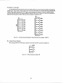
P6 - BaseAddress(FactorySetting:300hex (768decimal))
Oneof themostcommoncausesof failurewhenyou arefirst nying your boardis addresscontention.Someof
your computer'sI/O spaceis alreadyoccupiedby internalVO ando0rerperipherals.
WhentheAD1000board
attemptso useI/O addresslocationsalreadyusedby anotherdevice,contentionresultsand the boarddoesnot wolt.
To avoidthisproblem,theADl000 hasa headerconnector,P6, which les you selectany oneof eightsarting
addresses
in thecomputer'sI/O. Shouldthefactorysettingof 300hex (768decimal)be unsuitablefor your system,
you can selecta different baseaddress.Theseaddresses
are,from left o right on P6:
Hexadecimal
Declmal
200
512
240
576
280
640
2C0
704
300
768
340
832
380
896
3C0
960
To changethebaseaddresssetting,removethejumperfrom thefifth pair of pins (300hex)and,usingFigure
1-7asa guide,install it in thedesiredlocation.Recordthenewbaseaddresssettingon ttretableinsidetheback
coverof this manual.
o
o
ol
P6
o
\r
ol
C)
@
$l
o
o
ol
o
o
(r,
oooooooa
I
ooooaooo
o
ll
c,
o o
o
@
e) ci)
BASE
ADDRESS
P6
Fig.1-7- BaseAddress
Jumper,
1-8
P8 - End-of-ConvertMonitor (FactorySetting:8255PPI Port B, Bit 7)
Header
(EOC)signalcanbe usedto monitorthestatusof A/D conversions.
The A/D converter'send-of-convert
monitor
o
which
PPI
through
from
the
lines
you
choose
one
of
three
digital
les
Figure
1-8,
in
conn@torP8, shown
theEOC:Port A, bit 7 (PA7);PorrB, bit 7 (PB7);andPortC, bit ? (PC7).Oneof ilresethreelinesis selectedby
pair of pins.The selecteddigital line mustbe configuredasa
installinga jumper horizontallyacrosstheappropriate
(see
4).
Chapter
Mode0 input
r;]";
lr--ola
l..lc
P8
Jumper,P8
Fig.1-8- End-of-Convert
1-9
CHAPTER2
BOARD INSTALLATION
The AD1000boardis easyto installin your IBM PC/XT/AT or
compatiblecomputer.It canbeplacedin any slot, shoftor fullhow to install andconnect
size.This chaptertells you step-by-step
the board.
After you haveinstalledthe boardandmadeall of your connections,you canturn your systemon andrun the RTDDIAG
boarddiagnosticsprogramincludedon your examplesoftwaredisk
to verify that your boardis working.
2-1
2-2
Board Installation
Keepthe boardin its antistaticbag until you arereadyto install it in your computer.When removingit from the
bag,hold theboardat theedgesanddo not touchthecomponents
or connectors.
Beforeinstalling the boardin your computer,checkthejumper settings.Chapter1 reviewsthe factory settings
andhow to changethem.If you needto changeanysettings,referto theappropriateinstructionsin Chapter1.Note
thatincompatiblejumpersettingscanresultin unpredictable
boardoperationanderraticresponse.
To installtheboard:
1. Turn OFFthe powerto your computer.
2. Removethe top coverof thecomputerhousing(refero yourowner'smanualif you do not aheadyknow
how to do this).
3. Selectany unusedshortor full-sizeexpansionslot andremovetheslot bracket.
4. Touch the metalhousingof ttrecomputerto dischargeany staticbuildup and thenremovethe boardfrom its
antistaticbag.
5. Holdingtheboardby is edges,orientit sothatits cardedge(bus)connectorlinesup with theexpansionslot
conn@torin thebottomof theselectedexpansionslot.
6. After carefullypositioningtheboardin theexpansionslot sothat thecardedgeconnectoris restingon the
computer'sbusconnector,gentlyandevenlypressdownon theboarduntil it is securedin theslol
NOTE: Do not forcetheboardinto the slot.If theboarddoesnot slideino place,removeit andry again.
Wiggling theboardor exertingtoo muchpressure
canresultin damageo theboardor to thecomputer.
?. After theboardis installed,securetheslot bracketbackino placeandput thecoverbackon your computer.
The boardis now readyto be connectedvia the externalI/O connectorat therear panelof your comput€r.
External VO Connections
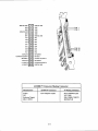
Figure2-l showstheADl000's P7 VO connectorpinout.Refero this diagramasyou makeyour VO connections.
ANALOG GND
DIGITALGND
AINE
AINT
AIN6
AINS
ANALOO OND
AIN4
AIN3
AIN2
AINl
DIGITALGItD
PA?
PA6
PA5
PA4
PA3
PA2
PAI
PAO
PC7
PC6
PC5
POI
PC3
pcl
PC0
PC2
EXTCLKO
EXTGATEO
CLKOUTO/CLKOUTO.
EXTCLKT
CLKOUTl/CLKOUTT.
EXTGATEI
EXTCIK2
EXTGATE2
+12VOLTS
.i2 VOLTS
CLKOUTZCLKOUT2DIGITALGNO
Fig.2-1-P7 VOConnector
PinAssignments
2-3
Connectingthe Analog Inputs
Connectthe high sideof eachanaloginput to oneof theanaloginput channels,AINI throughAIN8, and
connectthelow sideto anyoneof thetwo ANALOG GND signals@4-l or 7). Figure2-2 showshow theseconn@tions are made.
NOTE: It is goodpracticeto connectall unusedchannelsto ANALOG GND, asshownwith channel8 in ttre
diagrambelow.Failureto do somay affecttheaccuracyof your conversionresults.
1000
I/O CONNECTOR
P7
SIGNAL
SOURCE VOUT
1
GND
o
a
a
PIN 3
llprtlz'
. }OU CANCONNECTTHE GROUND
SIGNALSTO ANY ANALOGGNO PIN
(r oR 7)
rl
tv
Fig.2-2- AnalogInputConnection
Connectingthe Timer/Countersand Digital VO
For all of theseconnections,
the high sideof an externalsignalsourceor destinationdeviceis connectedto the
appropriatesignalpin on theI/O connector,andthelow sideis connectedto any DIGITAL GND.
Running the RTDDIAG DiagnosticsProgram
Now thatyour boardis ready[o use,you will wantto try it out. An easy-to-use
diagnosticsprogram,
RTDDIAG, is includedwith your examplesoftwareto helpyou verify your board'soperation.You canalsousethis
programto makesurethatyour curent baseaddresssettingdoesnot contendwith anotherdevice.
24
CHAPTER3
HARDWARE DESCRIPTION
This chapterdescribesthefeaturesof the AD1000hardware.
The majorcircuitsaretheA/D converter,the 8254timer/counters,
peripheralinterfacewhichprovides
andthe 8255programmable
the digital VO lines.Boardintemrptsarealsodescribedin this
chapter.
3-1
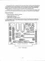
F
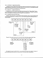
The ADl000 boardhasthreemajor circuits, the A/D converter,the timer/counters,and the programmable
peripheralinterface@PI) which providesthe digital I/O lines. Figure 3-1 showsthe block diagramof the boad.
intemrpls.
This chapterdescribeshardwarewhich makesup themajorcircuis. It alsodiscusses
Fig.3-1- AD1000
BlockDiagram
A/D ConversionCircuitry
conversions
on up to eightanaloginput channels.The following
The ADl000 boardperformsanalog-to-digital
paragraphs
A/D
circuiry.
the
describe
Analog Inputs
analoginput channelsareavailableon theAD1000board.The analoginput rangeis -5 to +5
Eight single-ended
+35
amplifierthroughan
Vdc overvoltageprotection.The channelsareconnectedto a sample-and-hold
volts,with
channel'sVO
writing
o
the
desired
software
by
is
through
The
channel
selected
active
multiplexer.
eight-channel
4.
port, asdescribedin Chapter
The SAI amplifiercapturesandholdsthe input signalat a constantlevel while theconvenionis performed,
ensuringrhatdynamic analogsignalsare accuratelydigitized. This capacitivecircuit quickly chargeso a level
to fte input voltagebeingsampledandholdsthechargefor thedurationof theconversion.The
corresponding
AD1000usesa .01gF low dielectriccapacitorwith a maximumacquisitiontime of 20 microseconds.
A/D Converter
The industrystandardHI574 ND converterperformsconversionsatarate of up to 50 kllz, or oneconversion
to
This conversiontime is addedto the SAI amplifier'sacquisitiontime of 20 microseconds
every20 microseconds.
J-J
give a boardmaximumthroughputrate of.25kl1z.The A/D outputis a l2-bit dataword which is outputin two 8-bit
canbe performedwhenspeedis morecritical thanresolution.Becausethe
bytes.Note that8-bit conversions
converteddatais containedin a single8-bit byte, 8-bit conversionstake about 13 microseconds,increasingthe
maximumboardttrroughputto about30 kHz.
Timer/Counters
0osupporta wide rangeof
intervaltimerprovidesthreel6-bit, 8 MIlz timerlcounters
An8254programmable
individually
for manyapplications,
used
These
can
be
cascaded
or
functions.
timer/counten
rimingandcounting
including tiggering an A/D conversionat a specifiedtime.
Eachtimer/counterhastwo inputs,CK in andGT in, and oneoutput, timer/counterOUT. The sourcesor
destinationsof the timer/counterVO canbe selectedusingjumperson headerconnectorP5 (seeChapterl). The
timer/counterscanbe programmedasbinary or BCD down countersby writing the appropriatedaa to the command
word, as describedin Chapter4. The commandword alsoles you set up the modeof operation.The six progam'
mablemodesare:
Mode0
Mode I
Mode 2
Mode 3
Mode 4
Mode 5
Event,Counter(Intenupton TerminalCount)
One-Shot
Hardware-Retriggerable
RateGenerator
SquareWave Mode
Software-TriggeredStrobe
HardwareTriggeredSrobe (Reniggerable)
Thesemodesaredetailedin ttre8254DataSheet,reprintedfrom Intel in AppendixC.
Digital VO, ProgrammablePeripheralInterface
periilheralinterface@PI)is usedfor digital I/O functions.This high-performance
The 8255programmable
TILICMOS compatiblechip has24 digitall/O linesdividedinto two groupsof 12lineseach:
GroupA - Port A (8 lines)andPort C Upper(4 lines);
GroupB - Port B (8 lines)andPort C Lower (4 lines).
Sixteenlines,Port A, Port,C lower, andPort C Upper,arebroughtout to theI/O connector.Port B's eightlines
areavailableat the P9 padson the board.You can usetheseportsin one of thesethreePPI operatingmodes:
Mode 0 - Basic inpuVoutput.Lets you usesimpleinput andoutput operationfor a porr Datais written !o or
readfrom the specifiedport.
Mode 1 - Strobedinput/output.Lets you EansferI/O datafrom Port A or Port B in conjunctionwitlt strobesor
signals.
handshaking
bidirectionallywith an externaldevice
L,esyou communicate
Mode 2 - StrobedbidirectionalinpuVourput.
is similarto Mode l.
throughPort A. Handshaking
Thesemodesaredetailedin ttre8255DataSheet,reprintedfrom Intel in AppendixC.
Interrupts
timerrcounter
outputs,PC3
intemrptsources:end-of-conver7,8254
The AD1000hasfour jumper-selectable
signal
(INTRA) from the 8255PPI,andanextemalintemrptbroughtontotheboardthroughP7. The end-of-convert
canbe usedto interrupt the computerwhenan A/D conversionis completed'The 8254 tinetlcounter intemrps can
be usedto generatevariousend-of-countintemrpB.The 8255PC3 intenupt canbe generatedwhenPPI Port A is
operatedin modeI or mode2, asexplainedon the 8255datasheet,AppendixC. The externalintemrptcanbe used
of how to useinterthatyou havean understanding
to generateintemrptsat any desiredinterval.We recommend
ruptsin your systembeforeyou connectan intenuptto an IRQ channel.Chapter4 providesa moredetaileddiscussionaboutintemtps.
34
CHAPTER4
BOARD OPERATIONAND PROGRAMMING
Thischaptershowsyou how to progmmanduseyourAD1000
board.It providesa completedescriptionof the VO map,a detailed
descriptionof programmingoperations,
anda flow diagramto aid
you in programming.The exampleprogrcmsprovidedon the disk
in your boardpackagearelistedat theendof this chapter.These
progmms,writtenin Turbo C, TurboPascal,andBASIC, include
sourcecodeto simplify your applicationsprogramming.
4-l
4-2
Definingthe VO Map
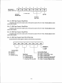
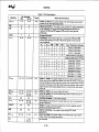
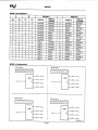
The VO mapfor the ADl000 is shownin Table4-1. As shown,theboardoccupies20VO port locations.The
baseaddress(designated
asBA) canbe selectedby changingttrejumperon headerconnectorP6,asdescribedin
Chapterl, Board Seuings.The followingsectionsdescribetheregistercontentsof eachaddressusedin the VO map.
Tabfe4.1- AD1000l/O
Map
ReglsterDescription
Channel
1 (AlN1)Select
ReadFunction
WrlteFunction
Addressr
(Decimal)
Reserved
Activatechannel1
B A +0
Channel
2 (AlN2)Select' Reserved
Activatechannel2
B A +1
(AlN3)Select
ChannelS
Reserved
Activatechannel3
BA+2
Channel4(AlN4)Select
Reserved
Activatechannel4
BA+3
Channel5(AlNs)Select
Reserved
Aclivatechannel5
B A +4
Channel6(AlN6)Select
Reserved
Activatechannel6
B A +5
Channel7 (AlN7)Select
Reserved
Activatechannel7
B A +6
ChannelS(AlN8)Select
Reserved
Activatechannel8
B A +7
Start12-bitA,/Dconversion
B A +8
Start8-bitA'lDconversion
BA+9
Start12-BitConversion/ Read A/D convededdata,
ReadData
MSB
Start8-BitConversion/
ReadData
ReadA/Dconvededdata,
LSB
Reserved
B A +1 0
Reserved
B A +1 1
PPIPortA
ReadPAO-PA7
digitall/O
digitall/O
ProgramPAO-PA7
B A +1 2
PPIPortB
ReadPB0-PB7digilall/O
ProgramPB0-PB7digitall/O
BA+13
PPlPorlC
ReadPCO-PC7
digitall/O
digitall/O
ProgramPCO-PC7
B A +1 4
PPlControlWord
Reserved
ProgramPPIconfiguration
B A +1 5
0
8254Timer/Counter
ReadTCOcountvalue
LoadTGOcountregister
B A +1 6
8254Timer/Counter
1
Read TC1 counl value
LoadTC1countregister
B A +1 7
2
S2S4TimerlCounter
ReadTC2countvalue
LoadTC2countregister
B A +1 8
8254ControlWord
' BA = BaseAddress
Reserved
Programcontrolregister
B A +1 9
BA + 0: Channel1(AINI) Select(Write Only)
Writing to this addressselectsanaloginput channelI (AINI). Thedatawrittenis irrelevanl After you select
channel1, it remainsactiveuntil you selectanotherchannelor powerdown.
BA + 1: Channel2 (AIN2) Select(Write Only)
Writing to this addressselectsanaloginput channel2 (AIN2). The datawrittenis irrelevanl After you select
channel2, it remainsactiveuntil you selectanotherchannelor powerdown.
BA + 2: Channel3(AIN3) Select(Write Only)
Writing to this addressselectsanaloginput channel3 (AIN3). The darawrittenis inelevant.After you select
channel3, it remainsactiveuntil you selectanotherchannelor powerdown.
+-J
BA + 3: Channel4(AIN4) Select(Write Only)
Writing to this addressselectsanaloginputchannel4(AIN4). The datawrittenis irrelevanLAfter you select
channel4, it.remainsactiveuntil you selectanotherchannelor powerdown.
BA + 4: ChannelS (AINS) Select(Write Only)
Writing to this addressselectsanaloginputchannel5 (AIN5). Thedatawrittenis irrelevanl After you select
channel5, it remainsactiveuntil you selectanotherchannelor powerdown.
BA + 5: Channel6(AIN6) Select(Write Only)
Writing to ttris addressselectsanaloginput channel6 (AIN6). The datawritten is irrelevant After you select
channel6, it remainsactiveuntil you selectanotherchannelor powerdown.
BA + 6: ChannelT (AIN7) Select(Write Only)
Writing to this addressselectsanaloginput channel7 (AIN7). The datawritten is irrelevant After you select
channel7, it remainsactiveuntil you selectanotherchannelor powerdown.
BA + 7: ChannelS (AIN8) Select(Write Only)
Writing to this addressselectsanaloginput channel8 (AIN8). Thedatawrittenis irrelevant After you select
channel8, it remainsactiveuntil you selectanotherchannelor powerdown.
BA + 8: Start l2-Bit Conversion/Read
MSB Data (Read/Write)
Writing to this addressstartsal?-bit A/D conversion(thedatawritten is irrelevant). A readprovidesttreMSB
(8 mostsignificantbits) of the l2-bit A/D conversion,asdefinedbelow.Theconverteddatais left-justified.When
you areperforming8-bit conversions,
only theMSB mustbe read.
MSB
D7
D6
D5
D4
D3
D2
D1
DO
12-Blt:
Bit11
Bit10
BitI
BirI
Bir7
Bit 6
Bit 5
Bir4
8-Bir:
Bir7
Bir6
Bir5
Bit4
Bir3
Bit2
Bir1
Bir0
BA + 9: Start 8-Bit Conversion/Read
LSB Data (Read/Write)
Writing to this addressstartsan 8-bit AID conversion(the datawritten is inelevant). A readprovidesthe I.SB
(4 leastsignificantbis) of the 12-bitA/D conversion,asdefinedbelow.Theconverteddatais left-justified.
LSB
D7
D6
D5
D4
Bh3
Bit2
Bitl
Bit0
D3
D2
D1
DO
BA + 10: Reserved
BA + 11: Reserved
BA + 12: PPI Port A - Digital VO (Read/Write)
Transfersthe 8-bit Port A digital input and digital outputdatabetweentheboard and an extemaldevice.A read
Eansfersdatafrom theexternaldevice,ttrroughP7, andinto PPI Port A; a write transfersthewrittendatafrom Port
A throughP7 to an extemaldevice.
+-{
BA + 13: PPI Port B - Digital VO (ReadAMrite)
Transfersthe 8-bit Port B digital input and digital outputdatabetweenthe boardand an externaldevice.A read
transfersdatafrom the externaldevice,o the on-boardpadsat P9, and ino PPI Port B; a write transfersthe wriuen
datafrom Port B throughthe on-boardpadsat P9 to an externaldevice.
BA + 14: PPI Port C - Digital UO (ReadAVrite)
Transfersthe two 4-bit Port C digitalinput anddigital outputdatagroups@ortC UpperandPort C Lower)
betweenthe boardand an extemaldevice.A readtransfersdatafrom the extemaldevice,tfuoughF/, and ino PPI
Port C; a write transfersthe written datafrom Port C throughP7 to an externaldevice.
BA + 15: 8255PPI Control Word (Write Only)
Whenbit 7 of this word is setto l, a write programsttrePPI configuration.When you want to monitor the endof-convertsignal throughP8, bit 7 of PPI Port A, B, or C, the PPI must be programmedso that the port usedis a
Mode 0 input porr
07
D6
D5
D4
D3
D1
DO
---1
-l
r
Mode Set F'"g
i
1 = active
I,
I
I
I
I
I
I
I
I
I
rde Seler;t
l= fllode
= mode
l= modg
i3it c
I
D2
I
I
I
I
PortA
0 = output
1 = input
|
I
|
lI l
I
PortB
0 = output
|
1 = input
|
I
ModeSelect
0=mode0
lr1=mode1
L
Port C Upper
0 = output
1 = input
Portc
t C Lower
0 - ooutput
ul
1 = input
inp
|
I
|
iytBJ
!ororpa
Whenbit 7 of thecontrolword is setto 0, a write canbe usedto individuallyprogmmthePort C lines.
D7
D6
D5
D4
D3
SeUReset
FunctionBit
0 = active
D2
Blt Select
000= PCO
001= pC1
010= PC2
0 1 1= P C 3
100= PC4
101= PC5
110=PC6
1 1 1= P C 7
D1
DO
Blt SeUReset
0=setbitto0
1=setbittol
For example,if you want to setPort C bit 0 to l, you would setup lhe controlword so thatbit 7 is 0; bits l, 2,
and3 are0 (this selectsPC0);andbit 0 is I (this setsPCOto l). Thecontrolword is setup like this:
4-5
X
Sets PCOto 1:
(writtento BA +15)
D7
SeUResel
Function
ion Bit
D6
D5
D3
D4
D2
D1
X = don'tcare
DO
Set PCO
Blt Select
000= PCO
BA + 16: 8254Timer/Counter 0 (Read/Write)
A readshowsthe countin thecounter,anda writ€ loadsthecounterwith a newvalue.Countingbeginsassoon
asthecountis loaded.
BA + 17: 8254Timer/Counter 1 (Read/Write)
A readshowsthecountin thecounter,anda write loadsthecounterwith a newvalue.Countingbeginsassoon
asthecountis loaded.
BA + 18: 8254Timer/Counter2 (Read/Write)
A readshowsthecountin thecounter,anda write loadsthecounterwith a newvalue.Countingbeginsassoon
asthe count is loaded.
BA + 19: 8254Timer/Counter Control Word (Write Onty)
Accessesthe8254controlregisterto directlycontrolthethreetimer/counters.
BCD/Blnary
0 = binary
1=BCD
CounterSelect
0
00 = Counter
01 = Counter1
2
10= Counter
11 = readbac*sening
Read/Load
00 = latchingoperation
01 = read/load
LSBonly
'10= read/load
MSBonly
11= Read/load
LSB,thenMSB
4-6
CounterModeSelect
000= Mclde0, evsntcount
001= Mode1, programmable
1-shot
010= Mode2, rategeneralor
011 = y96s 3, squarewavsratsgenerator
100= Mode4, software-triggered
strobe
101= Mode5, hardware-triggered
strobe
Programmingthe AD1000
This sectiongivesyou somegeneralinformationaboutprogrammingandtheAD1000board,andthenwalks
you throughthemajorAD1000programmingfunctions.Thesedescriptions
will helpyou asyou usetheexample
programsincludedwith theboardandtheprogrammingflow diagramat theendof this chapter.All of theprogarn
descriptionsin this sectionusedecimalvaluesunlessotherwisespecified.
The AD1000 is programmedby writing o and readingfrom the correctI/O port locationson the board.These
I/O portsweredefinedin theprevioussection.Most highJevellanguages
suchasBASIC,Pascal,C, andC+r, and
of courseassemblylanguage,makeit very easyto read/writetheseports.The tablebelow showsyou how to read
from and write to I/O ports using somepopularprogramminglanguages.
Language
Read
Data= INP(Address)
BASIC
Write
OUTAddress,Data
Data)
Data= inportb(Address) outportb(Address,
TurboC
TurboPascal
Assembly
Data:= Port[Address]
Port[Address]
:= Data
movdx,Address
in al,dx
movdx, Address
moval, Data
outdx, al
In additionto beingableto read/writetheI/O portson theAD1000,you mustbe ableto performa varietyof
operationsthat you might not normally usein your programming.The tablebelow showsyou someof the operaton
in this section,with an exampleof how eachis usedwith Pascal,C, andBASIC. Notethat the modulus
discussed
operatoris usedto retrievetheleas significantbyte(LSB) of a two-byteword,andtheintegerdivisionoperatoris
usedo retrievethe mostsignificantbyte (MSB).
Language
c
Modulus
o/o
2=bo/oC
IntegerDivision
I
a=b/c
AND
OR
&
a=b&c
I
a=blc
Pascal
MOD
a : = b M O Dc
DIV
a:=bDlVc
AND
a:=bANDc
OR
a:=bORc
BASIC
MOD
a=bMODc
\ (backslash)
a=b\c
AND
a=bANDc
OR
a=bORc
Many compilershavefunctionsthat canread/writeeither 8 or 16bits from/to an VO port For example,Turbo
PascalusesPort for 8-bit port operationsandPortW for 16bis, TurboC usesinportb for an 8-bit readof a port
andinport for a l6-bit read.Be sureto useonly 8-bit operationswith the AD1000!
Now thatyou know someof thelanguagebasics,we arereadyo look at theprogrammingstepsfor the
AD1000boardfunctions.
4-7
A/D Conversions
The following paragraphswalk you throughthe programmingstepsfor performingA/D conversions.You can
follow thesestepson the flow diagramat the end of this chapterand in our exampleprogramsincludedwith the
board.In thisdiscussion,BA referso thebaseaddress.
. Initializingthe AD1000
ThePPI mustbe
BeforeoperatingtheADl000, you may haveto initializethe 8255PPIand8254timer/counter.
1,
2
on
programmed
Mode
0,
or
operation,
depending
so that thedigital I/O linesarcsetup asinputsor outputs,
you
must
Port
B,
set
you
monitor
signal
through
bit
7,
your application.For example,if
theend-of-convert
wantto
=
(X
word
BA
+
15
care):
to
don't
up Port B asa Mode0 input.This is doneby writing thefollowingcontrol
D7
D6
D5
D4
D3
D2
D1
DO
If we replacetheXs (don't care)with zeros,thecommandin BASIC is:
our (BA + 15), 130
to definethedesiredmodeof operationif you areusinganyof the
The 8254timer/countermustbe programmed
The 8254is initializedby
OUT signalsasan interruptor whenusingthe8254for timing or countingoperations.
writing thecontrolword at BA + 19.Failureto initializethe8254whenan outputis connectedto an intemtpt
channelmaycauseerraticsystemoperation.
. Selectinga Channel
To selecta conversionchannel,you mustsimplywrite to theaddressport of thedesiredchannel,asshownin
Table4-1. The datawrittenis irrelevant.Notethatwhenthesystemis hrst poweredup, all channelsaredisabled.
After you progmma channel,it remainsactiveuntil you selectanotherchannel.
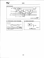
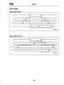
. Starting an A/D Conversion
A/D conversionsare stafiedby writing a START CONVERT commandto the appropriateI/O port. For 12-bir
Port BA + 9 is used.A START CONVERTcommandmust
Port BA + 8 is used.For 8-bit conversions,
conversions,
be writtenfor eachA/D conversion.Thedatawrittenis irrelevant.Figure4-1 showsthetiming diagramfor A/D
conversions.
StartConvert
A/D Status
Converting
NotConverting
Converting
Endof-Convert
ReadData
TimingDiagram
Fig.4-1- A/DConversion
4-8
Not Converting
. Monitoring ConversionStatus
The AlD conversionstatuscanbe monitoredthroughtheend-of-convert
@OC)signal.This signal,theinverse
of theSTATUSsignaloutputby the A/D converter,is low whena conversionis in progressandgoeshigh whenthe
conversionis completed.This low-o-high transitioncanbe monitoredthroughany oneof threePPI digital I/O lines,
PA7, PB7,or PC7,or throughan intemrptline.
. Readingthe ConvertedData
The generalalgorithm for mking an A/D readingis:
1. Starta 1,2-bitconversion.by
writing o BA + 8:
out base_address*8r 0
(Notethat thevalueyou sendis not important.Theactof writing to thisVO locationis thekey to
startinga conversion.)
2.Delayatleast20microseconds,
monitorPPIportA,
B, orC,bitTforatransition,
oruseanintemrpt
to ensurethat tle conversionis compieted.
3. Readtheleastsignificantbyteof theconverteddatafrom BA + 9:
Isb? = inp(base_addresst +9)
4. Readthemostsignificantbyteof theconverteddatafrom BA + 8:
msb? = inp(base_addresst +8)
5. Combinetheminto the l2-bitresultby shiftingthefourLSB bits o theright.TheMSB mustalso
be weightedcorrectly:
result? = (msb* * 16) + (lsbt/l-6)
.
For a 12-bitconversion,theA/D datiareadis left justifiedin a l6-bit word,with theleastsignificantfour bits
equalto zero.Becauseof this,the two bytesof A/D datareadmustbe scaledto obtaina valid AID reading.Onceit
is calculated,thereadingcanbe correlatedto a voltagevalueby subtractingZMB w scaleit andthenmultiplyingby
2.M14 millivolts.
For example,if theA/D readingis 1024,theanaloginputvoltageis calculatedasfollows:
(1024 - 2048) bits * 2.4414 mV/bit = -1.49999 volts.
Note that 8-bit A/D conversions
canalsobe performedby writing to VO locationBA + 9 to starta conversion.
While an 8-bit conversionhasa lowerresolution,it is performedmuchmorerapidly,in about13 microseconds.
A
l2-bit conversiontakesabout20 microseconds.
Thekey digital codesandtheirinputvoltagevaluesaregivenfor l2-bit and8-bit conversionsin ttrefollowing
two tables.
12-bit A/D BipolarCodeTable
8-bit A/D BipolarCodeTable
Input Voltage
OutputCode
InputVoltage
OutputCode
+4.9976votts
M S B11 1 1 1 1 1 1 1 1 1 1L S B
+4.9609volts
M S B 1 1 . I 11 1 1 1L S B
+2.500volts
1100 0000 0000
+2.500volts
1100 0000
0 volts
1000 0000 0000
0 volts
1000 0000
-2.500volts
0100 0000 0000
-2.500volts
0100 0000
-5.000volts
0000 0000 0000
-5.000volts
0000 0000
1 LSB= 2.44millivolts
1 LSB= 39.063millivolts
4-9
Interrupts
- What Is an Interrupt?
An interruptis an eventthatcausestheprocessor
in your computerto temporarilyhalt ifs curent p(rcessand
executeanotherroutine.Upon completionof thenewroutine,controlis retumedto theoriginalroutineat thepoint
whereits executionwasintemrpted.
Intemrptsarevery handyfor dealingwith asynchronous
events(eventsthatoccurat lessthanregularintervals).
Keyboardactivity is a goodexample;your computercannotpredictwhenyou mightpressa key andit wouldbe a
wasteof processortime for it o do nothingwhile waitingfor a keysnoketo occur.Thus,the intemrptschemeis
proceedswith othertasks.Then,whena keysrokedoesoccur,thekeyboard'intemrpts'the
usedandtheprocessor
processor,
processor
getsthekeyboarddata,placesit in memory,andthenreturnsto whatit wasdoing
andthe
beforeit wasinterrupted.Othercommondevicesthatuseintenups aremodems,disk drives,andmice.
Your AD1000boardcaninterruptt}reprocessorwhena varietyof conditionsaremet,suchasconversion
completed,timer countdownfinished,andothers.By usingtheseintemrpts,you canwrite softwarethateffectively
dealswith real world events.
- Interrupt RequestLines
To allow differentperipheraldevicesto generateinterruptson thesamecomputer,thePC bushaseightdifferent
intemrptrequest(IRQ) lines.A transitionfrom low to high on oneof theselinesgenerates
an intemrptrequest
which is handledby thePC's interruptcontroller.The intenuptcontrollercheckso seeif intemrptsareto be
from thatIRQ and,if anotherinterruptis alreadyin progress,it decidesif thenew requestshould
acknowledged
supersede
theonein progressor if it haso wait until theonein progressis done.This prioritizingallowsan
interrupt to be interruptedif the secondrequesthasa higherpriority. The priority level is basedon the numberof the
IRQ; IRQ0 hasthehighestpriority, IRQI is second-highest,
andso on throughIRQ7,which hasthelowest.Many of
IRQ0 is usedby the systemtimer,IRQ1 is usedby thekeytheIRQsareusedby thestandardgystemresources.
board,IRQ3 by COM2,IRQ4 by COMI, andIRQ6by thedisk drives.Therefore,it is importantfor you to know
which IRQ linesareavailablein your systemfor useby theAD1000board.
- E259ProgrammableInterrupt Controller
Thechip responsiblefor handlingintenuptrequestsin thePC is the 8259Programmable
IntemrptController.
To useinterrupts,you will needto know how to readandsetttre8259'sintenuptmaskregister(MR) andhow o
(EOI) commandto the8259.
sendttreend-of-interrupt
- Interrupt Mask Register(IMR)
Eachbit in the intemrptmaskregister(IMR) containsthemaskslatusof an IRQ line; bit 0 is for IRQO,bit I is
for IRQI, andso on. If a bit is set (equalto 1), thenfte corresponding
IRQ is maskedandit will not generatean
intemrpt If a bit is clear (equalto 0), thentheconesponding
IRQ is unmasked
andcangenerateintemrps.The
IMR is programmedthroughport 2lH.
IRQT
IRQ6
IRQs IRQ4 IRQ3 IRQ2 IRQl
IRQO
UOPort 21H
For all bits:
?=1H3ffi;li:!1tfi')
- End-of-Interrupt(EOI) Command
After an intemrptserviceroutineis completed,the8259interruptconEollermustbe notified.This is doneby
writing thevalue20H to I/O port 20H.
- What ExactlyHappensWhen an Interrupt Occurs?
to properlywrite software
thesequence
of eventswhenan interupt is riggeredis necessary
Understanding
(suchastheADl000), the
peripheral
line
is
high
device
When
an
intenupt
request
driven
interrupthandlers.
by a
4-10
interruptcontroller checksto seeif intemrptsareenabledfor that IRQ, and thencheckso seeif other intemrps are
which interrupthaspriority.The intenuptcontrollerthenintemrptstheprocesanddetermines
activeor requested
(CS),
instructionpointer(IP), andflagsarepushedon thestackfor slorage,anda new
The
code
segment
sor.
curent
loaded
from
that
a table
existsin thelowest1024bytesof memory.This tableis refenedto asthe
CS andIP are
is
intemrptvectortableandeachentry calledan intemrptvector.OncethenewCS andIP areloadedfrom the
interruptvectortable,theprocessorbeginsexecutingthecodelocatedat CS:IP.Whenthe intemrptroutineis
completed,theCS, IP, and flagsthatwerepushedon the stackwhenthe intemrptoccurredarenow poppedfrom the
stackandexecutionresumesfrom thepoint whereit wasintemrpted.
- Using Interrupts in Your Programs
Adding intemrptsto your softwareis not asdifficult as it may seem,and what they add in termsof performance
is oftenworth theeffort. Note,however,thatalthoughit is not thathardto useinterrupts,thesmallestmistakewill
often leadto a systemhangthat requiresa reboot.This canbe both frusrating and time-consuming.But, after a few
tries,you'll get thebugsworkedout andenjoythebenefitsof properlyexecutedintemrps.
- SpecialConsiderations
for AD1000Interrupt Programming
Two specialconsiderations
mustbe takeninto accountwhenusinginterruptson theADl000. First, you mustbe
very careful to makesurethat the 8259programmableintemrpt controller is properlyconfiguredto ignore intemrpts
becausethe 8254timer/countermustfirst be
on the selectedchannelimmediatelyafterpower-up.This is necessary
initializedto definethedesiredmode(s)of operation.Beforethe8254is initialized,its modes,counts,andouputs
areall undefined.If systemintemrptsarenot disabled,thecounteroutputsmaycauseenaticbehavior.
To usethe 8255PPI'sPC3intenupt,you mustenabletheinterruptby writing a "l" to theINTE maskbit in the
PPI controlword.This operationis fully describedin the 8255dau sheetincludedin AppendixC. Note thatthe
INTE maskis alwaysdisabledat power-upor resetandwhenevsrthe PPI modesare changed.
- IMriting an Interrupt ServiceRoutine(ISR)
The first stepin addingintemrptsto your softwareis to write the intemrpt serviceroutine (ISR). This is ttrc
routinethatwill automaticallybe executedeachtime an intenuptrequestoccurson thespecifiedIRQ. An ISR is
registersshouldbepushedontothe
differenttfranstandardroutinesthatyou write.First,on entrance,theprocessor
stackBEFORE you do anythingelse.Second,justbeforeexitingyour ISR, you mustwrite an end-of-intemrpt
(EOI) commandto the 8259intemrptcontroller.Finally,whenexitingtheISR, in additionto poppingall the
registersyou pushedon entrance,you mustusethe IRET instructionandnot a plain RET. The IRET automatically
popstheflags,CS, andIP thatwerepushedwhentheintemrptwascalled.
If you find yourselfintimidatedby intemrptprogramming,
takeheart.Most PascalandC compilersallow you
to identify a procedure(function) asan intemrpt type andwill auomatically addtheseinstructionsto your ISR, with
oneimportantexception:mostcompilersdo not automaticallyaddthe end-of-intemrptcommandto ttrcprocedure;
you mustdo this younelf. Otherthanthis andthefew exceptionsdiscussed
below,you canwrite your ISRjust like
in your programandit canaccessglobaldata.If you are
any otherroutine.It cancall otherfunctionsandprocedures
writing your first ISR, we recommendthatyou stick o ttrebasics;just somethingthatwill convinceyou thatit
works,suchasincrementinga globalvariable.
you areresponsible
for pushingandpopping
NOTE: If you arewriting an ISR usingassemblylanguage,
registersandusingIRET insteadof RET.
Therearea few cautionsyou mustconsiderwhenwriting your ISR.The mostimportantis, do not useany
DOS functions or routines that call DOS functionsfrom rvithin an ISR. DOS is not reentrant;that is, a DOS
functioncannotcall itself. In typicalprogramming,this will not happenbecauseof theway DOS is written.But
whataboutwhenusinginterrups?Then,you couldhavea situationsuchasthisin your program.If DOS functionX
is beingexecutedwhenan intenuptoccursandttreintenuptroutinemakesa call O DOSfunctionX, thenfunction
X is essentiallybeingcalledwhile it is alreadyactive.Sucha reentrancyattemptspellsdisasterbecauseDOS
iL Justmake
functionsaronot written to supportit. This is a complexconceptandyou do not needto understand
your
it is not
you
within
The
wrinkle
is
[hat,
unfortunately,
not
DOS
functions
from
ISR.
one
surethat
call any
do
obviouswhich library routinesincludedwith your compileruseDOS functions.A rule of thumbis thatroutines
4-ll
which write to thescreen,or checkthe statusof or readthekeyboard,andany disk VO routinesuseDOS andshould
be avoidedin your ISR.
The sameproblemof reentrancyexistsfor manyfloatingpoint emulatorsaswell, meaningyou may haveto
avoidfloatingpoint (real)mathin your ISR.
Notethattheproblemof reentrancyexists,no matterwhatprogramminglanguageyou areusing.Evenif you
arewriting your ISR in assemblylanguage,DOSandmanyfloatingpoint emulatorsarenot reenEant.Of course,
therearewaysaroundthisproblem,suchasthosewhichinvolvecheckingto seeif any DOS functionsarecurrently
activewhenyour ISR is called,but suchsolutionsarewell beyondthescopeof thisdiscussion.
The secondmajorconcemwhenwriting your ISR is to makeit asshortaspossiblein termsof executiontime.
Spendinglong periodsof time in your ISR may meanthatotherimportantintenuptsarebeingignored.Also, if you
spendtoo long in your ISR, it may be calledagainbeforeyou havecompletedhandlingthe first run.This oftenleads
to a hangthat requiresa reboot.
Your ISR shouldhavethis structure:
. Pushanyprocessorregistersusedin your ISR.Most C andPascalintenuptroutinesautomaticallydo this for
you.
. Put thebody of your routinehere.
. IssuetheEOI commandto the8259intenuptcontrollerby writing 20H to port 20H.
. Popall registerspushedon entrance.Most C andPascalintenuptroutinesautomaticallydo tttisfor you.
The following C andPascalexamplesshowwhattheshellof your ISR shouldbe like:
In C:
ISR(void)
void interrupt
{
/* Your code goes here. Do not use any DoS functions! */
outportb(Ox20, Ox20);
/* send Eor corffnandto 8259 */
In Pascal:
Procedure ISR,' Interrupt;
begin
{ Your code goes here.
port [$201 := $20;
end;
Do not
use any DOS functions ! )
{ Send EOI conmand to 8259 }
- Savingthe StartupInterrupt Mask Register(IMR) and Interrupt Vector
The next stepafterwriting the ISR is to savethesmrtupstateof ttreintenuptmaskregisterandthe intemrpt
vectorthatyou will be using.The IMR is locatedat I/O port 2lH. The intenuptvectoryou will be usingis located
in theinterruptvectortablewhich is simplyan arrayof 256-bit(a-byte)pointersandis locatedin thefint 1024
bytesof memory(Segment= 0, Offset= 0). You canreadthis valuedirectly,but it is a betterpracticeto usoDOS
function35H (getintenuptvector).Most C andPascalcompilersprovidea libraryroutinefor readingthevalueof a
vector.The vectorsfor thehardwareinterruptsarevectors8 through15,whereIRQOusesveclor8, IRQI uses
vector9, and soon. Thus,if the AD1000will be usingIRQ3,you shouldsavethevalueof intemrptvector 11.
Beforeyou installyour ISR,temporarilymaskout theIRQ you will be using.This preventstheIRQ from
requestingan interruptwhile you areinstallingandinitializingyour ISR.To masktheIRQ, readin the currentIMR
!o your IRQ (remember,
settinga bit disablesintemrps on thatIRQ
at I/O port 2lH andset the bit thatcorresponds
while clearinga bit enablesthem).The IMR is arrangedso thatbit 0 is for IRQO,bit I is for IRQI, andsoon. See
InterruptMaskRegister(IMR) earlierin this chapterfor helpin determiningyour IRQ's bit.
theparagraphentttJed
After settingthebit, write thenew valueto I/O port 2lH.
4-r2
With the startupIMR savedand the interruptson your IRQ temporarilydisabled,you can assignthe intemrpt
vectorto point to your ISR. Again,you canoverwritetheappropria@
entryin thevectorable with a directmemory
write, but this is a badpractice.Instead,useeitherDOSfunction25H (setintenuptvector)or, if your compiler
providesit, thelibrary routinefor settingan interruptvector.Rememberthatvector8 is for IRQO,vector9 is for
IRQ1,andsoon.
If you needto programthesourceof your interrupts,do ttratnext.For example,if you areusingtheprogrammableintervaltimer to generateintenupts,you mustprogramit to run in thepropermodeandat theproperrate.
Finally,clearthebit in theIMR for the IRQ you areusing.This enablesintenuptson theIRQ.
- Restoringthe StartupIMR and Interrupt Vector
Beforeexitingyour program,you mustrestorettreintemtptmaskregisterandintemrptvectorsto thestatethey
werein when your programstarted.To restorethe IMR, write the value that was savedwhen your programstarted
to I/O port 2lH. Restoretheintemrptvectorthatwassavedat startupwith eitherDOS function35H (getintenupt
vector),or usethe library routine suppliedwith your compiler.Performingthesetwo stepswill guaranteethat ttre
intemrpt statusof your computeris the sameafter runningyour programas it wasbeforeyour programstarted
running.
- CommonInterrupt Mistakes
. Rememberthathardwareintenuptsarenumbered8 through15,eventhoughfte corresponding
IRQsare
numbered0 through7.
. Oneof the mostcommonmistakeswhenwriting an ISR is forgettingto issuetheEOI commandto the8259
intemrptcontrollerbeforeexitingthe ISR.
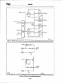
Timer/Counters
for timing andcounting
intervaltimerprovidesthreel6-bit, 8-MHz timer/counters
The 8254programmable
eventcounting,andintenupts.Figure4-2 showsthetimer/counter
functionssuchasfrequencymeasurement,
circuitry.
OUT. Theycanbe proEachtimer/counterhastwo inpus, CK in andGT in, andoneoutput,timer/counter
gammed asbinary or BCD down countersby writing the appropriatedatato the commandword, asdescribedin the
I/O mapsectionat thebeginningof thischapter.
Oneof two clock sources,theon-board5-MHz crystalor theexternalclock,canbejumperedastheclock input
canbe usedto clock thenexttimer/counterto
Or, theoutputfrom theprevioustimerrcounter
to eachtimer/counter.
a +5 volt.sourceandan
cascademultiplecounters.Two gatesourcesareavailablefor enablingthe timer/counters:
externalgatesource.The outpus areavailableat theP7 I/O connecorandinterruptheaderconnectorP3.
canbeprogrammedto operatein oneof six modes,dependingon your application.The
The timer/counters
paragraphs
describeeachmode.
briefly
following
Mode 0, Event Counter (Interrupt on Terminal Count).This modeis typicallyusedfor eventcounting.
While the timer/countercountsdown,theoutputis low, andwhenthecountis complete,it goeshigh.Theoutput
stayshigh until a new Mode0 controlword is writteno thetimer/countsr.
Mode l, Hardware-RetriggerableOne-Shot.The outputis initially high andgoeslow on fte clock pulse
following a triggerto begintheone-shotpulse.Theoutputremainslow until thecountreaches0, and$en goeshigh
andremainshigh until the clockpulseafterthenext trigger.
Mode 2, Rate Generator.This modefunctionslike a divide-by-Ncounterandis typicallyusedto generatea
to 1, the outputgoeslow for
real-timeclock intemrpt.The outputis initially high,andwhenthecountdecrements
goes
high again,tre timer/counter
reloadstheinitial count,andtheprocessis
oneclockpulse.The outputthen
This sequence
continuesindefinitely.
repeated.
4-13
825{ PIT
CLXOUTO/CLKOUTO.
o-l-----PrN
'bj-3!-ga
F-i
33
+ ExrGArEr
clKourr/clKourr-
I
Jr
E X T E R N AILN T E F R U P T I ^
-^ ^.
FnoM
PCBUS
I
z
RESET
Fig. 4-2 -
u
|
8254 Timer/CounterCircuitry
Mode 3, SquareWave Mode. SimilartLoMode2 exceptfor theduty cycleoutput,this modeis typicallyused
for baudrategeneration.Theoutputis initially high,andwhenthecountdecrements
to one-halfits initial count"the
reloadsandtheoutputgoeshighagain.This
outputgoeslow for theremainderof thecount.The timer/counter
processrepeatsindefinitely.
Mode 4, Software-TriggeredStrobe.The outputis initially high.Whentheinitial countexpircs,theouput
goeslow for oneclock pulseand thengoeshigh again.Countingis "triggered"by writing theinitial count
Mode 5, Hardware Triggered Strobe(Retriggerable).The outputis initially high.Countingis riggeredby
therising edgeof thegateinput.Whenthe initial counthasexpired,theoutputgoeslow for oneclockpulseand
thengoeshigh again.
For moreinformationaboutthe 8254,seethedatasheetincludedin AppendixC.
Digital UO
T\e24 digiul I/O linesin the8255canbe usedto transferdatabetweentle computerandexternaldevices.
Sixeen linesareavailableat the I/O connector;eightlines areavailableat theP9 on-boardpads.
For moreinformationaboutthe 8255,seethedatasheetincludedin AppendixC.
4-14
ExampleProgramsand Flow Diagrams
theuseof manyof theboard's
Includedwith ttreAD1000is a setof exampleprogramsthatdemonstrate
menu-driven
is an easy-to-use
Also
included
BASIC.
Pascal,
and
in
C,
in
written
features.Theseexamplesare
your
boardafter
out
you
first
checking
are
helpful
when
especially
program,
is
RTDDIAG, which
diagnostics
(Chapter
5).
installationandwhencalibratingtheboard
Beforeusingthe softwareincludedwith your board,makea backupcopyof the disk. You may makeasmany
backupsas you need.
C and PascalPrograms
Theseprogramsare sourcecodefiles so that you caneasily developyour own customsoftwarefor your
AD1000 board.In $reC direcory, thereare several.H files which areneededto implementthe main C programs.
Thesefiles containtheroutinescalledby the mainprograms.In thePascaldirectory,PSL files containall of the
procedures
neededto implementthemainPascalprograms.
Analog-to-Digital:
READ
how to takeAiD conversions.
Demonstrates
Timer/Counters:
TIMER
how to programthe 8254for useasa timer.
A shortpro$am demonstrating
Digital VO:
INPO
OUTO
Simpleprogramthatshowshow to setup thePPI linesasinput lines'
Simpleprogramthatshowshow to setup thePPI linesasoutputlines.
BASIC Programs
Theseprog&msincludesourcecodefiles for easycustomprogramdevelopment.
Analog-to-Digital:
READ
how to takeA/D conversions.
DemonsEates
Timer/Counters:
TIMER
how to programthe 8254for useasa timer.
A shortprogramdemonstrating
Digital VO:
INPO
OUTO
Simpleprogramthatshowshow to setup thePPI linesasinput lines.
Simpleprogramthatshowshow to setup thePPIlinesasoutputlines.
4-t5
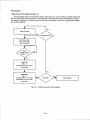
. SingleConvert Flow Diagram (Figure 4-3)
This flow diagramshowsyou thestepsfor aking a singlesampleon a selectedchannel.A sampleis takeneach
time you sendthe StartConvertcommand.All of thesampleswill be takenon thesamechanneluntil you selecta
new channel.ChangingtheI/O addressbeforeeachStartConvertcommandis issuedletsyou takethe nextreading
from a differentchannel.
ChangeChannel?
StartConversion:
BA+8for12-bit;
BA+9for8-bit
End-of-Convert
ReadLSB:
BA+9
(Contains
bitso-3of 12-bir
conversion)
ReadMSB:
BA+8
(Contains
bits4-11 of 12-bit
bils0-7of 8-bit
conversion;
conversion)
Stop Program
Fig.4-3- SingleConversion
FlowDiagram
4-16
CHAPTER5
CALIBRATION
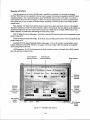
This chaptertells you how to calibratethe AD1000 using the
RTDDIAG calibration program included in the example software
packageand the two trimpots (TRl and TR2) on the board. These
trimpots calibrate the A/D converter gain and offset.
5-2
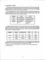
This chaptertells you how to calibratethe AID convertergain andoffset The offset and full-scaleperformance
readings,you cancheckthe
of theboard'sAfD converteris facory-calibrated.Any time you suspectinaccurate
UsingtheRTDDIAG
accuracyof yourconversionsusingtheprocedurebelow,andmakeadjussasnecessary.
programis a convenientway to monitorconversions
diagnostics
while you calibratetheboard.
Calibrationis donewith theboardinstalledin your PC. You canaccessthetrimpotswith thecomputer'scover
removed.Powerup thecomputerandlet theboardcircuitrystabilizefor 15minutesbeforeyou startcalibrating.
RequiredEquipment
The following equipmentis requiredfor calibration:
. hecision VoltageSource:-5 o +5 volrs
. Digital Voltmeter:5-12 digis
. SmallScrewdriver(for trimpotadjustment)
prograrn(includedwith examplesoftware)is helpful when
While not required,theRTDDIAG diagnostics
performingcalibrations.Figure5-l showstheboardlayout.The trimpos usedfor calibrationarelocatedin the
uppercenterareaof the board.
la
e,
t;
rct
m
rc5
R
m
m2
NA
gm
&T0
crcT0
o
o
o
o
o
o
o
o
o
'o
o
o
oo
oo
oo
oo
oo
oo
oo
oo
oo
oo
oo
tro
uto
lE-3
lk'! atl
rc7
m
m
R
m!
m
uo
ul
u2
lldol
llool
llool
|lt, {rl
rp.gl
l-li"EffiBmm
I
I li8"*?rsss-,"8ffi8"
o
Nr
I
o
16
l€
@;
''
A\ OOOOOOO
l"F;"
\7 Eroooooo
liU""odo*,,3Egr
19
rcotrrRor-sYsrsro ff
o*
a-"-
9"
6#r"
*
M;*L**oooooooooooooo
Real Timo Dovicss,Inc. StatoColl€gs,PA 16804 USA
Fig.5-1- BoardLayout
5-3
^r
pr
@
EH
Efl
@
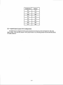
A/D Calibration
Two adjustrnents
aremadeto calibratetheAID converter.Oneis theoffsetadjustment,andttreotheris the full
TrimpotTR1 is usedto makettreoffsetadjustment,
andtrimpotTR2 is usedfor gain
scale,or gain,adjustment.
adjustment.Adjustmentsaremadeusing12-bitresolution.Table5-l shows*re idealinput voltagerangefor eachbit
weight.
Table5-1- A/D ConverterCalibrationTable
ldeal lnput Voltage,15V
(in mlllivolts)
A/DBit Weighr
4095(FullScale)
4997.6
2048
0000.0
1024
-2500.0
512
-3750.0
256
-4375.0
128
4687.s
64
-4843.8
32
-4921.9
16
-4960.9
I
,4980.5
4
-4990.2
2
4997.6
1
-5000.0
Useanaloginput channelI to calibratetheboard.Connectyour precisionvoltagesourceto channelI (positive
sideto P7-l I andgroundto P7-1or 7). Groundall otherchannels.Setthevolage sourceo 4.99878 vols, starta
conversion,andreadtheresultingdau. Adjustuimpot TRI until it flickersbetweenthe valueslistedin the table
below.Next, setthe voltagew +4.99634volts,andrepeattheprocedure,this time adjustingTR2 until thedaa
flickersbetweenthevaluesin thetable.
DataValueslor Calibrating-5 to +5 Volt Range
Offset(TR1)
ConverterGain(TR2)
Input Voltage= -4.99878V InputVoltage= +4.99634V
A/D ConvertedData
0000 0000 0000
0000 0000 0001
5-4
1 1 1 11 1 1 11 1 1 0
1 1 1 11 1 1 11 1 1 1
APPENDIX A
AD1OOO
SPECIFICATIONS
AD1000Characteristicsrypicat
@2s"c
Intertace
IBMPC/XT/AT
compatible
Jumper-selectable
baseaddress.l/O mapped
Jumper-selectable
interrupts
AnalogInput
8 single-ended
inputs
Inputimpedance,
eachchannel
........
lnputrange
protection
Overvoltage
Settling
lime.............
.............>10
megohms
t5 volts
..*35 Vdc
1 psec,max
A/DConverter...............
....Ht524
Type............
Resolution
Linearity
Conversion
speed..........
Sample-and-hold
acquisition
time
Throughput
Successive
approximation
...........
bits(guaranteed
........12
to 11bits)
...................*1
LSB,typ
psec,typ
..............20
psec,max
...................20
.25kHz
DlgltalilO.............
CMOS82Cs5
of lines
Number
(16
.........24 at UOconnector
& 8 on board)
High-level
output
voltage...................
....................4.2V,
min
voltage..................
Low-leveloutput
..................0.45V,
max
inputvoltage.
High-fevel
.2.2Y,min:.S.SV,
max
inputvoltage
Low-level
.-0.3V,min;0.8V,max
High-level
outputcurrent,lsource
100pA, max
outpulcurrsnt,1sink.,........
Low-level
1.7mA,max
drivecurrenl,I(DAR)
Darlington
1.0mA,min;-5.0mA,max
road
rnput
current
...........f:::::::::::::.T]::.::::.:::.:::itrlfl
lnputcapacitance,
1o
PF
MHz
"fi!)J"";Fl,[Tl;:
C(OUT)<@F=1
pF
.......20
TimeriCounter
.............
...........CMOS
82C54
Three16-bitdowncounters
Binaryor BCDcounting
Programmableoperatingmodes(6)..........................lnterruptonterminal
count; programmable
one-shot;rategenerator;
squarewaverategenerator;
software-triggered
strobe;
hardware-triggered
strobe
Counterinputsource
clock(8 MHz,max)or
...........
External
on-board5 MHzclock
outputs
Counter
...............Avai1ab1e
externally;
usedas PC interrupts
or
source
counrer
sare
..............*::::::
fl?::J,?Ht:;
always enabled
(PCbus-sourced)
Mlscellaneous
lnputs/Outputs
*12 volts
Digitalground
CurrentRequirements
+5 volts
+12volts......
-12 volts
........68
mA
20 mA
......28
mA
A-3
Connector
40-pin,
rightangle,shrouded
header
withejector
tabs
Slze
(99mm
Shortslot- 3.875"H
x 5.40"W
x 137mm)
A-4
APPENDIX B
CONNECTORPIN ASSIGNMENTS
B-2
ANALOG GND
D I G I T A LG N D
AINS
AINT
AIN6
AIN5
ANALOG GNO
AIN4
AIN3
AIN2
AINl
DIGITALGND
PA7
PA5
PA5
PA4
PA3
PA2
PA1
PAO
PCi
PC6
PC5
PC4
PC3
PC2
PC1
PC0
EXTCLKO
CLKOUTO/CLKOUTO.
EXTGATEl
EXTCLK2
EXTGATEO
EXTCLKl
CLKOUTl'CLKOUT1.
EXTGATE2
+12 VOLTS
CLKOUT2/CLKOUT2.
-12 VOLTS
O I G I T A LG N D
AD1000P7 Connector/MatingConnector
Manufacturer
ADf000 P7 Connector
P7 Mating Connector
Fujitsu
3M
RobinsonNugent
MrL C-83503
FCN-705Q040-AUA4
FCN-7078040-AU/B
3417-7M0
IDS-C4OPK-C.SR-TG
M83503/7-09
B-3
APPENDIX C
COMPONENTDATASHEETS
c-l
c-2
IntervalTimer
Intel82C54Programmable
DataSheetReprint
intel'
82C54
TIMER
INTERVAL
CHMOSPROGRAMMABLE
I Compatlblewith all Intel and most
other mlcroprocessors
r Hlgh Speed,'%eroWalt State"
Operationwlth 8 MHz8086/88and
80186/188
I HandlesInputsfrom DCto 8 MHz
- 10 MHzlor 82C54-2
r AvallableIn EXPRESS
- StandardTemperatureRange
- Ertended TemperatureRange
I Threeindependent16-bitcounters
I Low PowerCHMOS
- lcc : 10 mA @8 MHzCount
frequencY
I CompletelyTTL Compatlble
CounterModes
r Slx Programmable
r Binaryor BCDcounting
r StatusReadBack Gommand
I AvallableIn 24-PlnDIPand 28-PlnPLCC
CHMOSversionof the industrystandard8254 counter/timerwhich is
The lntel 82C54is a high-performance,
systemdesign.lt providesthree
designedto solve the liming control problemscommonin microcomputer
MHz. All modesare software
10
up
to
independent16-bitcounters,each capableof handlingclock inputs
programmable.
The 82C54is pin compatiblewith the HMOS8254,and is a supersetof the 8253.
Six programmabletimer modesallow the 82C54to be used as an event counter,elapsedtime indicator,
programmableone-shot,and in many other applications.
The 82C54 is fabricatedon Intel's advancedCHMOSlll technologywhich provides low power consumption
with performanceequal to or greaterthan the equivalentHMOSproduct.The 82C54 is availablein 24'pin DIP
and 28-pin plastic leaded chip canier (PLCC)packages.
s
6
t
t
9
l0
tl
t2t3rt|tIltt.
231241-3
PIISTIC LEADEDCHIPCARRIER
otl
I
Dl
2
t
a
03
Dr
Or
231244-1
Ycc
2i2
m
m
21
e5
20
Ar
D,
I
It
lo
Or
,
tt
clt
Do
I
tt
oura
,CLI O
t
OIJT O
OTTE O
Flgure1.82C54BlockDlagram
aa
t3
t0
lrt
oxo l t z
2
o^tc 2
clx I
OATET
ogT I
Diagramsare for pin tef6renc€only.
Packagesiz€sar€ not to scel€.
Ffgure2.82C54Plnout
3-83
S.PtsmbGr1989
Ordcr ilumbcn 2312't4'005
82C54
Table1.PlnDescrlption
Symbol
PlnNumber
DIP
PLCC
Dz-Do
1-8
2-9
CLK O
I
10
11
10
I
12
o
I
o
Powersuoolvconnection.
Ground:
Out1:Outputof Counter1
't6
13
14
16
17
18
19
Data:Bidirectionaltri-state
databus lines,
connectedto systemdatabus.
Clock0: Glockinputof Counter0.
Output0: Outputof Counter0.
Gate0: Gateinputof Counter0.
17
OUTO
GATEO
GND
OUT1
GATE1
CLK1
GATE2
ouT2
CLK 2
At, Ao
12
13
14
15
't8
tlo
I
I
I
Gate 1: Gateinputof Counter1.
20
o
2.
Out2: Outputof Counter
21
I
I
Clock2: Clockinputof Counter2.
20-19
23-22
6
21
24
RD
22
26
WR
23
27
Vcn
24
NC
Function
Type
Clock1:Clockinputof Counter1
Gate2: Gateinputof Counter2.
Address:
Usedto selectoneof thethreeCounters
ortheControtWordRegisterfor reador write
to thesystem
Normally
connected
operations.
addressbus.
Selects
A1
As
Counter0
o
0
1
Counter1
0
Counter2
1
0
Reqister
ControlWord
1
1
ChipSelectA lowonthisinputenablesthe82C54
to respondto FiDandWRsignals.FiDandWFiare
ignoredotheruise.
ReadControl:This inputis low duringCPUread
ooerations.
WriteControl:Thisinputis low duringCPUwrite
operations.
Power:* 5V powersupplvconnection.
28
1,11,15,25
NoConnect
sired delay.After the desireddelay,the 82C54 will
interruptthe CPU.Softwareoverheadis minimaland
variablelengthdelayscan easilybe accommodated.
DESCRIPTION
FUNCTIONAL
General
intervaltimer/counter
The82C54is a programmable
designedfor use with Intel microcomputersystems.
elementthat can
It is a generalpurpose,multi-timing
be treated as an array of l/O ports in the system
software.
The 82C54solvesone of the most commonproblems in any microcomputersystem,the generation
of accuratetime delays under software control. lnsteadol setting up timing loops in software,the programmerconfiguresthe 82C54to matchhis requirementsand programsone of the countersfor the de-
Someof the other counter/timerfunctionscommon
to microcomputers
which can be implementedwith
the 82C54 are:
r
o
o
.
o
o
.
r
3-84
Realtimeclock
Evencounter
Digitalone-shot
rate generator
Programmable
Squarewave generator
Binaryrate multiplier
Complexwaveformgenerator
Complexmotorcontroller
intef
82C54
BlockDlagram
CONTROLWORDREGISTER
DATABUSBUFFER
This 3-state,bi-directional,
8-bitbutteris usedto interfacethe 82C54to the systembus(seeFigure3).
The ControlWordRegister(seeFigure4) is selected
by the Read/WriteLogicwhenAr, Ao : 11. lf the
CPU then does a write operationto the 82C54,the
data is stored in the ControlWord Registerand is
interpretedas a ControlWord used to define the
operationof the Counters.
The ControlWord Registercan only be writtento;
status informationis availablewith the Read-Back
Command.
231244-4
Flgure3. BlockDlagramShowlngDataBus
Bufferand Read/WrlteLogicFunctlons
231214-5
READ/WRITELOGIC
The Read/WriteLogicacceptsinputsfromthe syscontrolsignalsfor the other
tem busandgenerates
funclionalblocksof the 82C54.Ar and As select
one of the threecountersor theControlWordReg
into.A "low" on the RD
ter to be readfrom/written
inputtells the 82C54that the CPll_isreadingoneol
the counters.A "low" on the WR inputtells the
82C54that the CPUis U[!ng eithera ControlWord
by
or an initialcount.BothRDandWRarequalified
F; FD and WFiare ignoredunlessthe 82C54has
beenselectedby holdingCSlow.
Flgure 4. Block Dlagram Showing Control Word
Begister and Counter Functlons
COUNTERO,COUNTER1, COUNTER2
Thesethreefunctionalblocksare identicalinoperation, so only a singleCounterwill be described.The
internalblock diagramof a singlecounteris shown
in Figure5.
The Countersare fully independent.Each Counter
may operate in a differentMode.
Tne ControlWord Registeris shown in the figure;it
is not part of the Counteritself, but its contents determine how the Counteroperates.
3-85
82C54
storedin theCRandlatertransfenedto the CE.The
ControlLogicallowsone registerat a time to b€
loadedfromthe internalbus.Bothbytesare transCRt,tand CR1are
ferredto the CE simultaneously.
In this
clearedwhenthe Counteris programmed.
for one
way,if the Counterhas beenprogrammed
byteonlyor least
bytecounts(eithermostsignilicant
significantbyte only) the other byte will be zero.
Notethatthe CEcannotbe writteninto;whenevera
countis written,it is writtenintotheCR.
TheControlLogicis alsoshownin thediagram.
CLK
to the outn, GATEn, andOUTn areallconnected
sideworldthroughthe ControlLogic.
82C54SYSTEMINTERFACE
231214-6
Flgure5. Internal Block Diagramof a Counter
The status register, shown in the Figure, when
latched,containsthe currentcontentsof the Control
Word Register and status of the output and null
count flag. (See detailed explanationof the ReadBack command.)
TheactualcounterlslabelledCE (for "CountingElement"). lt is a 16-bit presettablesynchronousdown
counter.
The 82C54 is treatedby the systemssoftware as an
arrayof peripherall/O ports;threeare countersand
the fourth is a control regisler for MODE programming.
Basically,the selectinputsA9,A1 connectto the A9,
41 addressbus signalsof the CPU.The CS can be
deriveddirectlyfrom the addressbus using a linear
select method.Or it can be connectedto the output
of a decoder,such as an lntel 8205 for larger systems.
OLM and OL1 are two 8-bit latches. OL stands for
"Output Latch"; the subscripts M and L stand for
"Most significantbyte" and "Least significantbyte"
respectively.Both are normally referred to as one
unitand calledjust OL. Theselatchesnormally"follow" the CE, but if a suitableCounterLatch Commandis sent to the 82C54,the latches"latch" the
presentcount until read by the CPU and then return
to "following" the CE. One latch at a time is enabled
by the counter's Control Logic to drive the internal
bus.This is how the 16-bitGountercommunicates
over the 8-bit internal bus. Note that the CE itself
cannot be read; wh€never you read the count, it is
the OL that is being read.
Similarly,there are two 8-bit registers called CRy
and CRg (for "Count Register").Both are normally
refened to as one unit and called just CR. When a
new count is written to the Counter, the count is
3-86
l
Ao
c3
' couxlct
oi2
OUI OAIE CLi
DrOr
aacra
cottTEi
'OUl
CAt€ Crx'
t!
9l
coutrct
Out cl?E clx'
231241-7
Flgure6.82C54System Interlace
iffier
DESCRIPTION
OPERATIONAL
the 82C54
Programming
General
Countersare programmedby writinga ControlWord
and then an initialcount.The controlwordformatis
shownin Figure7.
After power-up,the state of the 82C54is undefined.
The Mode, count value,and outputol all Counters
are undefined.
How each Counteroperatesis determinedwhen it is
programmed.Each Counler must be programmed
before it can be used.Unusedcountersneednot be
programmed.
All ControlWords are written into the ControlWord
Register,whichis selectedwhen A1, Ao : 11. The
ControlWord itselfspecifieswhich Counteris being
programmed.
By contrast,initialcountsare writteninto the Counters, not the ControlWord Register.The A1, Ag inputs are used to select the Counter to be written
into. The format of the initial count is determinedby
the ControlWordused.
ControlWord Format
A1,A6:11 FS:0
FD:t
D7
WR:0
D5
sc1 sc0
D5
Da
D3
D2
Ds
D1
RW1 RW0 M2 M1 MO BCD
SC- SelectCounter:
M - IIODE:
M2
scl
sco
0
0
SelectCounter
0
0
0
0
Mode0
0
1
SelectCounter1
0
0
1
Mode1
1
0
SelectCounter2
X
1
0
Mode2
1
1
Read-BackGommand
(SeeReadOperations)
X
1
1
Mode3
1
0
0
Mode4
1
0
1
Mode 5
RW - Read/Write:
RWl RWo
0
0
CounterLatchCommand(see Read
Operations)
0
1
0
1
Read/Writeleastsignificantbyteonly.
1
0
Read/Writemostsignificantbyteonly.
1
1
Read/Writeleastsignificantbytefirst,
then mostsignificantbyte.
BinaryCounter
16-bits
BinaryCodedDecimal(BCD)Counter
(4 Decades)
NOTE: Don't care bits (X) shouldbe 0 to insure
compatibilitywith lulure htel products.
Flgure7. ControlWordFormat
3-87
intet
82C54
structionsequenceis required.Any programming
aboveis acthatfollowstha conventions
sequencs
ceptable.
WriteOperations
procedurefor the 82C54is very
The programming
flexible.Onlytwo conventionsneed to be remembered:
1) For each Counter,the ControlWord must be
writtenbeforethe initialcountis written.
2) The initialcount must follow the count lormat
specifiedin the ControlWord (leastsignificant
byteonly,mostsignificant
byteonly,or leastsignificantbyteandthenmostsignificantbyte).
Sincethe ControlWord Registerand the three
Countershaveseparateaddresses(selectedby the
A1,Aoinputs),
andeachControlWordspecifies
the
Counterit appliesto (SCo,SC1bits),no specialinControlWord- Counter0
LSBof countCounter0
MSBof count- Counter
0
- Counter1
ControlWord
LSBofcount- Counter1
MSBof count- Counter1
ControlWord- Counter
2
LSBof countCounter2
MSBof count- Counter
2
ControlWord- Counter0
Counter
Word- Counter1
ControlWord- Counter2
LSBof countCounter2
LSBof countCounter1
LSBof countCounter0
MSBof count- Counter
0
MSBof count- Counter1
MSBol count- Counter
2
A1
1
0
0
1
0
0
1
1
1
A0
1
0
0
1
1
1
1
0
0
A1
1
1
As
1
1
0
0
0
0
1
A newinitialcountmay be writtento a Counterat
any time without affecting the Counter's programmed
Modein anyway.Countingwill be atfected
Thenewcount
in theModedefinitions.
asdescribed
mustfollowthe programmed
countformat.
to read/writetwo-byte
lf a Counteris programmed
precaution
applies:A program
counts,the following
mustnot transfercontrolbetweenwritingthe first
andsecondbyteto anotherroutinewhichalsowrites
intothatsameCounter.
the Counterwill
Othenrise,
be loadedwithan incorrect
count.
A1
11
11
11
10
10
01
01
00
00
Aq
2
Counter
Counter1
0
Counter
Counter
2
Counter
2
Counter1
Counter1
0
Counter
0
Counter
A1
11
11
01
11
00
01
10
00
10
A6
ControlWord- Counter1
- Counter0
ControlWord
LSBof count
Counter1
GontrolWord- Counter2
LSBof countCounter
0
MSBof count- Counter1
LSBof count2
Counter
MSBof count- Counter
0
MSBof count- Counter2
ControlWord
ControlWordControlWord
LSBof count
MSBof countLSBof countMSBof countLSBof countMSBof count-
1
1
1
0
1
0
0
1
0
NOTE:
In all four examples,all countersare programmedto readlwritetwo-bytecounts.
Theseare only four of manypossibleprogrammingsequences.
Figure8. A FewPosslbleProgramming
Sequences
ReadOperations
It is often desirableto read the value of a Counter
withoutdisturbingthe countin progress.This is easily done in the 82C54.
There are three possible methods lor reading the
counters: a simple read operation, the Counter
Latch Command,and the Read-BackCommand.
Eachis explainedbelow.The first method is to perform a simple read operation.To read the Counter,
which is selectedwith the A1, A0 inputs, the CLK
input of the selectedCountermust be inhibitedby
usingeitherthe GATE input or external logic. Otherwise,the count may be in the proc€ssof changing
when it is read,givingan undefinedresult.
3-88
int€t
82C54
grammingoperationsof other Countersmay be inserted betweenthem.
COUNTERLATCH COMMAND
The second methoduses the "CounterLatchCommand". Likea GontrolWord,thiscommandis written
to the Control Word Register,which is selected
when A1, Ao : 11. Also like a ControlWord,the
SCO,SC1 bits selectone of the threeCounters,but
two other bits, D5 and D4, distinguishthiscommand
from a ControlWord.
Another feature of the 82C$4 is that reads and
writes of the same Countermay be interleaved;for
example,if the Counteris programmedfor two byte
counts,the followingsequenceis valid.
1. Read least significantbYte.
2. Write new leastsignificantbyte.
3. Read most significantbYte.
4. Write new most significanlbyte.
A r ,A o : 1 1 ; 6 : 0 ; F D : t ; W F : 0
D5 Da D3 D2 D1 Ds
sc1 sc0 0 0 X X X X
D7
lf a Counter is programmedto read/write twebyte
counts,the fotlowingprecautionapplies;A program
must not transler control between readingthe lirst
and secondbyte to anotherroutinewhichalso reads
from that same Counter.Othenvise,an incorrect
counl will be read.
D5
SC1, SCo - specifycounterto be latched
sc1 sco
0l0l
0l1l
1l0l
1 |
1
Counter
0
1
2
| Read-BackCommand
READ.BACKCOMMAND
The third method uses the Read-Backcommand.
This commandallows the user to check the count
value, programmedMode, and cunent state of the
OUT pin and Null Countflag of the selectedcounte(s).
D5,D4- 00 designatesCounterLatchCommand
X - don't care
NOTE:
Don'tcare bits (X) shouldbe 0 to insurecompatibility
withfuturelntelproducts.
The commandis writtenintothe ControlWordRegister and has the format shown in Figure 10. The
command applies to the counlers selected by setbits D3,D2,D1: 1.
ting their corresponding
Figure 9. Counter l-atching CommandFormat
A0,Al:il
The selectedCounter'soutputlatch(OL)tatchesthe
count at the time the Counter Latch Commandis
received.This countis held in the latchuntilit is read
by the CPU (or until the Counteris reprogrammed).
The count is then unlatchedautomaticallyand the
OL returnsto "following"the countingelement(CE).
This allows reading the contents of the Counters
"on the fly" without affectingcountingin progress.
MultipleCounterLatch Commandsmay be usedto
latch more than one Counter. Each latched Counter's OL holds its count untilit is read.CounterLatch
Commandsdo not affect the programmedMode of
the Counterin any way.
lf a Counter is latched and then, some time later,
latched again before the count is read, the second
Counter Latch Commandis ignored.The count read
will be the count at the time the first CounterLatch
Commandwas issued.
With either method, the count must be read according to the programmed format; specifically,if the
Counter is programmed for two byte counts, two
bytes must be read.The two bytes do not haveto be
read one right atter the other; read or write or pro-
e5:0
FD:i
WF:0
Da
1
1
D
EOUNTST TUSCNT2 CNT 1 CNTO 0
D5:Q : Latch count of selectedcounter(s)
Da:0 : Lalch statusof selectedcounter(s)
D3: t : Selectcounter2
D2: 1 : Selectcounter1
D1:1 : Selectcounler0
D9:Reservedfor futureexpansion;must be 0
Figure 10.Read-BackCommandFormat
The read-backcommandmay be usedto latch multiple counter output latches (OL) by setting the
COUNTbit D5:0 and selectingthe desiredeounte(s). This single command is functionallyequivalent to several counter latch commands, one lor
each counter latched. Each counter's latchedcount
is held until it is read (or the counter is reprogrammed).That counter is automaticallyunlatched
when read, but other countersremain latched until
they are read. lf multiplecountread-backcommands
are issued to the same counterwithout readingthe
3-89
intet
82C54
count,all but the first are ignored;i.e.,the count
whichwill be readis the countat the timethe first
read-back
commandwasissued.
THISACTION:
A. Wrile to the control
r.r
wororeglsler:rrr
B. Writelo the counl
r"gitt"i (cn)rP]
C. Newcountis loaded
inlocE (cR --+ cE);
Theread-backcommandmayalsobe usedto latch
statusinformation
of selectedcounter(s)by setting
ffi'ns- bit D4:0. Statusmustbe latchedto be
read;statusof a counteris accessedby a readfrom
thatcounter.
D5
D6 D3 D2 D1 Ds
NULL
RW1 RW0 M2 M1 MO BCD
COUNT
OutPinisl
OutPinis0
N u l lc o u n t
Countavailablefor reading
CounterProgrammedMode (See Figure7)
Nullcount:0
Flgure12.NullCountOperation
Both count and status of the selected counter(s)
may be latched simultaneouslyby setting both
mmT anoSIFfUSbitsD5,D4:0.Thisis functionally
thesameasissuing
twoseparate
read-back
Flgure 11.Status Byte
NULL COUNTbit D6 indicateswhen the last count
writtento the counterregister(CR)has been loaded
into the countingelement(CE).The exact time this
happensdependson the Modeof the counterand is
describedin the ModeDefinitions,
but untilthe count
is loadedinto the countingelement(CE),it can't be
readfrom the counter.lf the countis latchedor read
beforethis time, the countvaluewill not reflectthe
new countjust written.The operationof Null Count
is shownin Figure12.
Command
D7 D5 D5 Da D3 D2 D1 Ds
Nullcount:1
lf multiplestatus latch operationsof the counter(s)
are performedwithoutreadingthe status,all but the
first are ignored;i.e.,the status that will be read is
the statusof the counterat the time the tirst status
read-backcommandwas issued.
OUTPUT
D7t =
0:
D 51 :
0 :
Ds-Do
Nullcount=1
[tl OnU the counterspecifiedby th€ control word will
have its null count set to 1. Null count bits of other
countersare unaffecled.
I2l r the counteris programmedfor two-byte counts
(least significantbyt€ th€n most significantbyte) null
countgoes to 1 whEnthe secondbyle is written.
Thecounterstatusformatis shownin Figure11.Bits
D5 throughD0 containthe counter'sprogrammed
Modeexactlyas writtenin the last ModeControl
Word.OUTPUTbit D7 containsthe currentstateof
the OUTpin. This allowsthe userto monitorthe
counter'soutputvia sottware,possiblyeliminating
somehardwarefroma system.
D6
CAUSES:
commandsat once,and the above discussionsapply here also. Specifically,if multiplecount and/or
statusread-backcommandsare issuedto the same
counter(s)withoutany interveningreads,ali but the
first are ignored.This is illustratedin Figure13.
lf bothcountand statusof a counterare latched,the
firstreadoperationof that counterwill returnlatched
status,regardlessof which was latched first. The
next one or two reads (dependingon whether the
counteris programmedfor one or two rype :ounts)
returnlatchedcount. SubsequentreaCoreturn unlatchedcount.
Descrlptlon
Besultc
1
1
0
0
0
0
1
0
Readbackcountand stafusof
Counter0
Countand statuslatched
for Gounter0
1
1
1
0
0
1
0
0
Readbackstatusof Counter1
Statuslatchedfor Counter1
1
1
1
0
1
1
0
0
Readback statusof Counters2, 1 StatuslatchedforCounter
1
't
0
1
1
0
0
Countlatchedfor Counter2
1
1
0
0
0
1
0
0
Readbackcountof Counter2
0
Readbackcountand statusot
Counter1
Countlatchedfor Counter1,
but not status
1
1
1
0
0
0
1
0
Readbackstatusol Counter1
Command
ignored,
status
latchedforCounter1
already
2,butnotCounter1
Figure13.Read-BackCommandExample
3-90
inbf
G
0
0
82C54
Thisallowsthe countingsequenceto be synchronized by sottware.Again,OUT does not go highuntilN
+ 1 CLK pulsesaftertne new count of N is written.
RD WR At Ao
1
0
0 WriteintoCounter
0
0
1
1 WriteintoCounter1
0
0
lf an initial count is written while GATE = 0, it will
still be loadedon the next CLK pulse.WhenGATE
goes high,OUT will go high N CLK pulseslater;no
CLKpulseis neededto load the Counteras thishas
alreadybeen done.
0
1
0
1
0
WriteintoCounter2
0
t
0
1
1
WriteControlWord
0
0
1
0
Readfrom Counter0
0
0
1
0
0
1
ReadfromCounter1
0
0
1
1
0
0
U
1
1
1
1
X
X
0
1
1
X
X
X
X
ReadfromCounter
2
(3-State)
No-Operation
(3-State)
No-Operation
(3-State)
No-Operation
Flgure14.Read/WrlteOperatlons
Summary
ModeDefinitions
The lollowingare definedfor usein describing
the
operationof the 82C54.
CLKPULSE:arisingedge,thena fallingedge,in
thalorder,of a Counter's
CLKinput.
TRIGGER:
a risingedgeof a Counter's
GATEinput.
COUNTER
transfer
LOADING:the
of a countfrom
the cR to the cE (referto
the "FunctionalDescription")
l-l,.l-1" l3 | ll i ll I I lslt:l
CUr l0
Ltl rl
ltl.
e
MODE0: INTERRUPT
ONTERMINAL
COUNT
Mode0 is typicallyusedforeventcounting.
Afterthe
ControlWordis written,OUTis initiallylow,andwill
remainlowuntiltheCounter
reaches
zero.OUTthen
goeshighand remainshighuntila newcountor a
new Mode0 ControlWordis writtenintothe Counter.
GATE : 1 enablescounting;
GATE: 0 disables
counting.GATEhasno effecton OUT.
AftertheControlWord
andinitialcountarewritlento
the initialcounlwillbe loadedon thenext
a Counter,
CLKpulse.ThisCLKpulsedoesnotdecrement
the
count,so for an initialcountof N, OUTdoesnotgo
highuntilN + 1 CLKpulsesaftertheinitialcountis
written.
lf a new countis writtento the Counter,it will be
loadedon the nextCLKpulseandcounting
willcontinuefromthe newcount.ll a two-bytecountis written,the followinghappens:
1) Writingthefirstbytedisables
counting.
OUTis set
(noclockpulserequired).
low immediately
2) Writingthe secondbyteallowsthe newcountto
be loadedon the nextGLKpulse.
3-91
l- l- l- l* lSlt I I ll ll ls l:il
231244-8
NOTE:
The FollowingConventionsApply To All Mode Timing
Diagrams:
1. Counters are programmedfor binary (not BCD)
countingand for Reading/Wrilingleast significantbyte
(LSB)only.
2. The counteris alwaysselected(eS alwayslow).
3. CW standsfor "ControlWord"; CW : 10 meansa
controlword ol 10, hex is writtento the counter.
4. LSBstandslor "Leasi SignificantByte" ol count.
5. Numbersbelowdiagramsare count values.
The lowernumberis the least significantbyte.
The upper number is the most significantbyte. Since
the counter is programmedto R€ad/Write LSB only,
the most significantbyte cannotbe read.
N standslor an undelinedcount.
Verticallines show transitionsbetweencount values.
Figure15.Mode 0
intef
82Cs4
MODE2: RATE GENERATOR
IIODE 1: HARDWARERETRIGGERABLE
ONE.SHOT
OUTwillbeinitiallyhigh.OUTwillgo low on the CLK
putsefotlowinga triggerto begin the one-shotpulse,
and will remain low until the Counter reacheszero'
OUTwillthen go high and remainhigh untilthe CLK
pulse after the next trigger.
After writingthe ControlWord and initialcount,the
Counteris armed. A trigger results in loadingthe
Counterand settingOUT low on the next CLK pulse,
thusstartingthe one-shotpulse.An initialcountof N
will resultin a one-shotpulseN CLK cyclesin durahence OUT will
tion. The one-shotis retriggerable,
remainlow for N CLK pulsesafter any trigger.The
one-shotpulsecan be repeatedwithoutrewritingthe
samecount into the counter.GATE has no etfect on
OUT.
lf a new countis writtento the Gounterduringa oneshot pulse,the currentone-shotis not affectedun'
less the Counter is retriggered.In that case, the
Counteris loaded with the new count and the one'
shot pulse continuesuntil the new count expires.
This Modefunctionslike a divide-by'Ncounter.lt is
typiciallyused to generatea Real Time Clock inter'
rupt.OUf will initiallybe high.When the initialcount
has decrementedto 1, OUT goes low for one CLK
pulse.OUT then goes high again, the Counter reioads the initialcount and the processis repeated.
Mode 2 is periodic;the same sequenceis repeated
indefinitely.For an initialcount of N, the sequence
repeatsevery N CLK cYcles'
GATE : 1 enablescounting;GATE : 0 disables
counting.lf GATEgoes low duringan output pulse,
OUT is set high immediately.A trigger reloads the
Gounterwith the initialcounton the next CLK pulse;
OUT goes low N CLK pulsesafter the trigger.Thus
the GATE input can be used to synchronizethe
Counter.
After writinga ControlWord and initial count, the
Counterwll[ be loadedon the next CLK pulse.OUT
goes low N CLK Pulsesafter the initialcount is written. This allowsthe Counterto be synchronizedby
softwarealso.
FT
cLt
oltE
oul
l0lolFFl0l0l
lr
l0lFFlr
lr
I
WI
cLr
GAIE
ouT
0l0
r 12
LSI -l
wt
ct,(
GA'E
lor0l
l.,tl
231244-'tO
out
liirlnir
,_.t0t0l0lfFlFFt0lol
r"lalrlolrrlFcl.Jrl
23't244-9
Figure16.Mode 1
Figure17.Mode 2
inbf
82C54
Writing a new count while countingdoes not atfect
the current counting seguence. ll a trigger is received after writing a new count but before the end
of the current period,the Gounterwill be loadedwith
the new count on the next CLK pulseand counting
will continue from the new count. Othenrrise,the
new count will be loaded at the end of the cunent
countingcycle. In mode 2, a COUNTof 1 is illegal.
OUTwill be highfor (N + 1l/2 countsand low for
(N -1)/2 counts.
"aa
M---l--l
rtODE 3: SQUAREWAVE MODE
Mode 3 is typicallyused for Baud rate generation.
Mode 3 is similarto Mode2 exceptfor the dutycycle
of OUT. OUT will initiallybe high.When half the initial count has expired,OUT goeslow for the remainder of the count. Mode 3 is periodic;the sequence
above is repeated indefinitely.An initial count of N
results in a square wave with a period of N CLK
cycles.
".: :::
--l-]
".
After writing a Control Word'and initialcount, the
Counterwill be loadedon the next CLK pulse.This
allows the Counterto be synchronizedby software
also.
Mode 3 is implementedas follows:
Even counts:OUT is initiallyhigh.The initialcountis
loaded on one CLK pulse and then is decremented
by two on succeedingCLK pulses.Whenthe count
expires OUT changesvalue and the Counteris reloaded with the initialcount. The above processis
repeatedindefinitely.
Odd counts: OUT is initiallyhigh. The initialcount
minus one (an even number)is loadedon one CLK
pulse and then is decrementedby two on succeeding CLK pulses. One CLK pulse after the count expires, OUT goes low and the Counter is reloaded
with the initial count minus one. SucceedingCLK
pulses decrementthe count by two. Whenthe count
expires, OUT goes high again and the Counter is
reloadedwith the initialcountminusone.The above
process is repeated indefinitely.So lor odd counts,
I-l
r:r:I: r:| : r:r3| r r:r:I
aaa
GATE : 1 enablescounting;GATE : 0 disables
counting.ll GATEgoes low whileOUTis low,OUTis
set high immediately;no GLK pulse is required.A
triggerreloadsthe Counterwith the initialcount on
the neld CLK pulse. Thus the GATE input can be
used to synchronizethe Counter.
Writinga new count while countingdoes not affect
the current counting sequence.lf a trigger is received atter writinga new count but beforethe end
of the current half-cycleof the square wave, the
Counter will be loaded with the new count on the
next CLK pulse and countingwill continuefrom the
new count. Othenrise,the new countwill be loaded
at the end of the cunent half-cycle.
l-l
l'l.lrl-l:
l-l
ltl:ltltl!l:i:
ll:l!l
231211-11
NOTE:
A GATEtransitionshouldnot occur one clock prior to
terminalcount.
Figure18.Mode 3
MODE4: SOFTWARETRIGGEREDSTBOBE
OUT will be initiallyhigh.When the initialcount expires,OUT will go low for one CLK pulse and then
go high again.The countingsequenceis "triggered"
by writingthe initialcount.
GATE : 1 enablescounting;GATE : 0 disables
counting.GATE has no effecton OUT.
After writing a Control Word and initial count, the
Counterwill be loadedon the next CLK pulse.This
CLK pulse does not decrementthe count, so for an
initial count of N, OUT does not strobe low until
N + 1 CLK pulsesatterthe initialcountis written.
lf a new count is writtenduringcounting,it will be
loadedon the nert CLK pulseand countingwill continue from the new count. lf a two-bytecount is writ-
ten,thefollowinghappens:
3-93
inbf
82C54
After writing the Control Word and initial count, the
counterwill not be loadeduntilthe CLK pulseafter a
trigger. This CLK pulse does not decrement thE
count, so for an initialcount of N' OUT does not
strobelow until N + 1 CLK pulsesafter a trigger'
1)Writingthe firstbytahasno effecton counting.
2) Writingthe secondbyteallowsthe newcountto
be loadedon the nextCLKPulse.
This aflowsthe sequenceto be "retriggered"by
software.OUTstrobeslow N* 1 CLK pulsesafter
the newcountof N is written.
A triggerresultsin the Counterbeingloadedwith the
initialcount on the next GLK pulse. The counting
OUT will not strobe low
sequenceis retriggerable.
for N * 1 CLK pulsesafter any trigger.GATE has
no effecton OUT.
m
lf a new countis writtenduringcounting,the current
countingsequencewill not be affected.lf a trigger
occurs after the new count is written but before the
crrrrentcount expires,the Counterwill be loaded
with the new count on the next CLK pulse and
countingwill continuefrom there.
cLt
cart
our
0lFrlFFlFFl
0 lFFlFErF0l
n
rt
ctr
CLT
oAtt
6^rt
OUT
out
l" l" l" l- l3 | 3li l3l? l3 l:[l
Ctrll
L3lrt
l5!r2
TI
ET
CLI
cLr
GA'E
GAIE
oul
out
l.l'.l"l-l3l
ololo
ilri2
I o I o I F FI
rxlr l'lrl"l'l:l
lrl0lF;l
231244-12
cs:t^
Figure19.Mode 4
Lsa=3
ll3
ll lis i::i
Lst,!
WE
ctx
IIIODE5: HARDWARETRIGGEREDSTROBE
(RETRIGGERABLE)
Glt€
OUT wilt initiallybe high.Countingis triggeredby a
risingedge of GATE.When the initialcount has expired,OUT will go low for one CLK pulse and then
go highagain.
OUI
lr "r rl t. t t t a r|t t o t lF*F t flt"t 3 r Ia lo I o l o I o l r r i r r l
"
231244-13
Flgure 20. Mode 5
3-94
o, o I
intet
82C54
Slgnal
Statur
llodes
Low
Or Golng
Low
0
Disables
countine
OperationCommonto All Modes
Rlslng
Programming
Enables
countino
3
1) Disables
counting
2) Setsoutput
immediately
hioh
'l) Disables
counting
2) Setsoutput
immediately
hioh
4
When a Control Word is written to a Gounter,all
ControlLogicis immedialelyresetand OUT goesto
a known initialstate; no CLK pulsesare requiredfor
this.
1) Initiat€s
counting
2) Resetsoutput
afternext
clock
1
2
Hlgh
GATE
lnitiates
counting
Enables
counling
lnitiates
counting
Enables
counting
Disables
countinq
The GATE input is always sampledon the rising
edgeof CLK.In Modes0,2,3, and 4 the GATEinput
is level sensitive,and the logic level is sampledon
the risingedgeof CLK.In Modes1,2,3, and 5 the
GATEinputis rising-edge
sensitive.In theseModes,
a rising edge of GATE (trigger)sets an edge-sensitiveflip-ftopin the Counter.Thisflip-flopis then sampleo on the next risingedge of CLK; the flip-flopis
reset immediatetyafter it is sampled.ln this way, a
triggerwill be detected no matterwhen it occurs-a
highlogicleveldoes not haveto be maintaineduntil
the next rising edge of CLK. Note that in Modes 2
and 3, the GATE input is both edge-and level-sensitive. ln Modes2 and 3, if a CLK sourceother than
the system clock is used, GATE should be pulsed
immediately
lollowingWR of a new countvalue.
Enables
counting
5
lnitiates
counting
Flgure21.GatePinOperations
Summary
COUNTER
mAx
iltN
[IODE
COUNT COUNT
0
1
1
1
0
0
2
3
2
0
2
0
4
1
0
New counts are loaded and Counters are decrementedon the fallingedge of CLK.
The largestpossibleinitialcount is 0; this is equivalent to 216 for binary countingand 104 for BCD
counting.
NOTE:
0 is equivalentto 216 for binarycountingand 104 lor
BCDcounting
Figure22.Mlnimumand MaxlmumInitlalCounts
The Counterdoes not stop when it reacheszero. In
Modes0, 1, 4, and 5 the Counter"wrapsaround"to
the highestcount,eitherFFFFhex for binarycounting or 9999 for BCD counting,and continuescounting. Modes2 and3 are periodic;the Counterreloads
itself with the initial count and continues counting
from there.
3-95
intel
82C54
'Notice: Sfressesabovethoselisted under'Abso
lute MaximumRatings"maycausepermanentdam'
age to the device.Thisis a str€ssrating only and
functionaloperationof the device at these or any
otherconditionsabovethoseindicatedin the opera'
tionalsectionsof thisspecificationis not implied.Fx'
posure to absotutemaximumrating conditionsfor
ertendedperiodsmayaffect devicareliability.
ABSOLUTEMAXIMUMRATINGS*
UnderBias.' . . . . .0'Cto 70'C
Temperature
Ambient
StorageTemperature .....-65'to +150'C
......-0.5to +8.0V
SupplyVoltage
..... +4Vto *7V
OperatingVoltage
.GND-2V to *6.5V
Voltage
on anylnput..
Voltage
on anyOutput. .GND-0.5Vto V6s + 0.5V
. . .1 Watt
PowerDissipation
D.C.CHARACTERISTICS
Temperature)
10%,GND:0V)fin : -40oCto t85"C for Extended
(fA:0'C to 70'C,Vcc:svt
Symbol
Vu
Vrs
Vor
Vox
Parameter
InoutLowVoltaqe
InputHighVoltage
OutputLowVoltage
OutputHighVoltage
Mln
-0.5
Mar
0.8
2.O
!1-.1 * 0.5
0.4
3.0
Ven - 0.4
Unlts
V
V
V
V
V
pA
x2.o
166
lnpuiLoadCurrenl
Currenl
OutputFloatLeakage
V66 SupplyCunent
20
rrA
mA
lccsa
V66 SupplyCurrent-StandbY
r0
pA
I11
lopr
r10
Vg6SupplyCurrent-StandbY
150
pA
Clru
Crro
InputCapacitance
pF
cour
OutputCapacitance
10
20
20
lccsgr
l/O Caoacitance
pF
pF
TeetCondltlonr
lor : 2.5mA
loH : -2.5 mA
lon = - 100p.A
Vrrrr=Vecto 0V
Vorrr:Vcc to 0.0V
Freq: '#ly;rrrTl
crk
CLKFreq : 96
eS: Vcc.
BusV66
All Inputs/Data
AllOutputsFloating
CLKFreq : 96
6 : Vcc.AllOtherInputs,
l/O Pins: V6ND,OutputsOPen
lc:1MHz
pins
Unmeasured
to GND(5)
returned
A.C.CHARACTERISTICS
:0V) (Tn : -40"C to +85"Cfor Extended
Temperature)
Ol : 0'C to 70'C,Vcc : 5V t1O%, GND
(Note1)
BUSPARAMETERS
READCYCLE
Symbol
Parameter
tlR
AddressStableBeforeRD-J
tsn
FiDJ
G staoleBefore
tRn
AddressHoldTimeAfterFD T
RDPulseWidth
DataDelayiromFiDI
tnn
tno
tlo
tor
tRv
Data Delayfrom Address
RD-f to DataFloating
Time
Recovery
Command
82C51
Mln
45
0
0
Max
150
5
200
NOTE:
1. AC timingsmeasuredat V6s = 2.0V,V61 = 0.8V'
3-96
120
220
90
82C54-2
Max
Mln
30
0
0
95
5
165
Unlta
ns
ns
ns
ns
85
ns
185
ns
65
ns
ns
intet
82C54
(continued)
A.C. CHARACTERISTICS
WRITECYCLE
tRw
AddressStableBeforeWF J
tsw
WRt
eS stauteBefore
twl
HoldTimeAfterWFt
Address
WFiPulsewidth
DataSetupTimeBeforeWFif
DataHoldTimeAfterWF f
rww
tow
two
tnv
82Cs4
Parameter
Symbol
ilin
0
llax
0
0
150
120
0
200
CommandRecoveryTime
82C54-2
Min
Max
0
0
0
95
95
0
165
Units
82Cs4-2
Units
ns
ns
ns
ns
ns
ns
ns
CLOCKANDGATE
Symbol
tcrx
tpwx
tpwl
Ts
tp
tew
tcu
Parameter
ClockPeriod
HighPulseWidth
Low PulseWidth
ClockRiseTime
ClockFallTime
GateWidthHigh
Gate Width Low
tos
tcx
GateSetupTimeto CLKT
Ton
OutputDelayfromCLKJ
tooe
twc
twe
OutputDelayfrom GateJ
CLK Delayfor Loading(a)
GateDelayfor SamPling(a)
two
tcr-
OUTDelayfromModeWrite
GateHoldTimeAfterCLKT
CLKSet Up for CountLatch
82C54
Max
Min
125
DC
60(3)
60(3)
25
25
50
Min
100
30(3)
50(3)
50
50
50
50(2)
40
50(2)
0
-5
100
0
-5
100
55
40
240
-40
40
260
-40
45
DC
25
25
50
150
120
55
50
Mar
ns
ns
ns
ns
ns
ns
ns
ns
ns
ns
ns
ns
ns
ns
ns
NOTES:
2. ln Modes 1 and 5 triggersare sampledon each risingclock edge.A secondtriggerwithin 120 ns (70 ns lor the 82C54-2')
ol the risingclock edgemaynot be detecled.
3. Low-goingglitchesthat violatetpWH,tpWl may causeenors requiringcounterreprogramming.
below.
4. Exceptfor ExtendedTemp.,See ExtendedTemp.A.C.Characteristics
5. Samplednot 100%tested.T1 : 25'C.
6. lf CLK presentat Twg min then GountequalsN+2 CLK pulses,Try6 max equalsCountN*1 CLK pulse.Tyy6min to
Tyy6max,countwill be eitherN + 1 or N + 2 CLK pulses.
7. ln Modes 1 and 5, i{ GATEis presentwhen writinga new Countvalue,at Tyy6min Counlerwill not be triggered,at Try6
max Counterwill be iriggered.
8. lf CLK presentwhen writinga CounterLatch or ReadBackCommand,at T61 min CLK will be reflectedin count value
latched,at T61 max CLK will not be reflectedin the @unt valuelalched.Writinga CounterLatch or BeadBackCommand
betweenT6s min and Tyysmax will resultin a latchedcountvalluewhich is + one leasl significantbit.
40"C to + 85'C for ExtendedTemperature)
EXTENDEDTEMPERATURE
CT
82C54
82Cs4-2
' Parameter
Symbol
Min
twc
twc
CLK Delayfor Loading
-25
llax
25
GateDelayforSampling
-25
25
3-97
Min
-25
-25
llax
25
25
Unlts
ns
ns
intef
291244-11
291241-15
RECOVERY
231244-16
inbf
CLOCKAND GATE
?3121j-17
' Llst byl€ ot counl being writlen
A.C. TESTINGINPUT.OUTPUTWAVEFORM
A.C.TESTINGLOADCIRCUIT
INPUT/OUTPUT
,,0
2.0
\,t
t\
0.t
> Ttlr rorxrt <
0.1
2312U-18
A.C.Testing:Inputsar€ drivenat 2.4Vtor a logic"1" and 0.45V
for a logic"0." Timingmeasur€m€nts
aremad€at 2,0Vtof ! logb
"1" and 0.8Vfor a logic"0."
I
oertc.
I
utocl
l?rtrll
|
I
|
FI c r .
+
llrt
Gl = 150PF
Gs includesllg cspecitance
231211-19
PeripheralInterface
Intel82C55AProgrammable
DataSheetReprint
intel'
82C55A
INTERFACE
PERIPHERAL
CHMOSPROGRAMMABLE
Capability
I ControlWord Read-Back
I Direct Bit Set/ResetCaPabllitY
r 2.5 mA DC DriveCapabilityon all l/O
Port Outputs
I Availablein 40-PinDIP and 44-PinPLCC
r Availablein EXPRESS
- StandardTemperatureRange
- ExtendedTemperatureRange
I Compatiblewith all Inteland Most
Other Microprocessors
r High Speed,"Zero Wait State"
Operationwith I MHz8086/88and
8 0 1 8 6 /1 8 8
l/O Plns
a 24 Programmable
r Low PoweTCHMOS
r CompletelyTTL Gompatible
GHMOSversionof the industrystandard82554 generalpurpose
The Intel 82C55Ais a high-performance,
ll provides
programmablel/O devicewhichis designedfor use with all lntel and most othermicroprocessors.
programmedin 2 groupsof 12 and usedin 3 majormodesof operation.
24l/O pins whichmay be individually
The 82C55Ais pin compatiblewith the NMOS8255Aand 8255A'5.
ln MODE O, each group ol 12llo pins may be programmedin sets ol 4 and I to be inputsor outputs.In
to haveI linesof inputor output.3 of the remaining4 pinsare used
MODE1, each groupmay be programmed
bus configuration.
for handshakingand interruptcontrolsignals.MODE2 is a strobedbi-directional
The 82C55Ais fabricatedon lntel'sadvancedCHMOSlll technologywhich provideslow powerconsumption
with performanceequalto or greaterthan the equivalentNMOSproduct.The 82C55Ais availablein 40-pin
DIP and 44-pinplasticleadedchip carrier(PLCC)packages.
r e3 i i 3 c i 3 ! 3 r c
7
tfs€l
I
oo
0r
,
A0
?c,
ic
&
rc5
ro
D!
rc
l2
:3
D'
D5
06
H
m
r6
17
ttltSzEEtS!
'
!:1c55
Figure1.82C554Block Diagram
Figure2.s2cssA;;t:tu;
Oiagramsare lor pin referene only.Package
sizesare nol to scale.
3-124
t9tt
S.pt.mbd
Ordor llumbe:231256S4
82C55A
Table1.PlnDescripilon
Symbol
PAs-o
PlnNumbcr
Dlp
PLCC
1-4
2-5
m
5
6
e3
6
7
GND
7
I
Ar-o
8-9
9-10
Typc
Nameand Functlon
t/o
PORTA, PINS0-3: LowErnibbteof an B-bitdata outputlatch/
bufier and an 8-bitdatainput latch.
READ CONTROL:This inputis low duringCpU read operations.
I
I
CHIPSELECT:
A lowonthisinputenabtes
theB2CS5A
to
respondto FiEandWFIsignats.
ffi andWRareignored
otherwise.
SystemGround
ADDRESS:
Theseinputsignats,
in conjunction
RE andWFi,
controltheselection
of oneof thethreeportsor the controt
wordregisters.
Ar
As
WF G
Input Operatlon (Read)
0
0
0
1
0
PortA-DataBus
0
1
0
1
0
PortB-DataBus
1
0
0
1
0
PortC-DataBus
1
1
- DataBus
0
1
0
ControlWord
OutputOperatlon(Wrlte)
0
0
1
0
0
DataBus- PortA
0
1
1
0
0
DataBus- PortB
1
0
1
0
0
DataBus- PortC
1
1
1
0
0
DataBus- Control
DisableFunctlon
X
X
x
X
1
DataBus-3-State
X
X
1
1
0
DataBus-3-State
m
PCz-l
1 0 - 1 3 1 1 , 1 3 - 1 5 t/o
PCo-s
PBo-z
14-17
16-19
t/o
18-25
20-22,
24-28
vo
PORTB, PINS0-7: An 8-bitdataoutputtatch/bufferand an 8_
bil data inputbuffer.
SYSTEMPOWER:* 5V powerSuppty.
t/o
DATA BUS:Bi-directional,
tri-statedata bus lines,connectedto
systemdatabus.
RESET:A highon thisinputclearsthe controlregisterand ail
ports are set to the inputmode.
WRITECONTROL:Thisinputis low duringCpU write
operations.
Vcc
Dz-o
26
29
27-34
30-33,
3s-38
RESET
35
39
WH
36
40
I
37-40
41-44
t/o
PAz-n
NC
1,12,
23,34
PORTC, PINS4-7: Uppernibbleof an g-bitdata outputlatch/
bufferand an 8-bitdata inputbuffer (no latch for input).This port
can be dividedintotwo4-bitportsunderthe modecontrol.Each
4-bitportcontainsa 4-bitlalchand it can be usedfor the control
signaloutputsand statussignalinputsin conjunctionwith ports
A and B.
PORTC, PINS0-3: Lowernibbteof port C.
PORTA, PINS4-7: Uppernibbleof an 8-bitdata outputtatch/
butferand an 8-bitdatainputlatch.
No Connect
3-125
intef
82C55A
DESCRIPTION
82C55AFUNCTIONAL
General
peripheralinterface
The 82C55Ais a programmable
sysdevicedesignedfor use in Intelmicrocomputer
tems. lts functionis that of a generalpurposel/O
componentto interfaceperipheralequipmentto the
microcomputersystembus. The functionalconfigurationof the 82C55Ais programmedby the system
softwareso that normallyno exlernailogicis necessary to interlaceperipheraldevicesor structures.
Data Bus Buffer
This 3-statebidirectional
8-bitbutferis usedto interface the 82C55A to the systemdata bus. Data is
transmittedor receivedby the bufleruponexecution
of inpul or output instructionsby the CPU.Control
words and status informationare also transferred
throughthe data bus buf{er.
Read/Write and Control Logic
The function of this block is to manageall of the
internal and external translers of both Data and
Controlor Statuswords. lt'acceptsinputsfrom the
CPUAddressand Gonlrolbussesand in turn,issues
commandsto both ol the GontrolGroups.
Group A and Group B Controls
The functional configurationof each port is programmedby the systemssoftware.In essence,the
CPU "outputs" a controlword to the 82C55A.The
control word containsinformalionsuch as "mode",
"bit set", "bil reset", etc., that initializesthe functional configurationol lhe 82C55A.
Each of the Controlblocks (GroupA and GroupB)
accepts"commands"from the Read/WriteControl
Logic, receives"control words" from the internal
data bus and issuesthe Propercommandsto its as'
sociatedports.
ControlGroupA - PortA and PortC upper{C7'C/.')
ControlGroupB - PortB and PortC lower(C3-C0)
The control word register can be both written and
read as shown in the addressdecode table in the
pin descriptions.Figure6 shows the control word
format tor both Read and Write operations.When
the controlwordis read,bit D7 will alwaysbe a logic
"1", as this impliescontrolword mode information.
Ports A, B, and C
The 82C55Acontainsthree8-bitports (A, B, anctC).
All can be configuredin a wide varietyof functional
characteristicsby the systemsoftwarebut each has
its own special features or "personality" to further
enhancethe powerand flexibilityof the 82C55A.
Port A. One 8-bit data output latch/butfer and one
8-bit input latch butfer. Both "pull-up" and "pull'
down" bus hold devicesare Presenton Port A.
Port B. One 8-bit data input/output latch/butfer.
Only "pull-up"bus hold devicesare presenton Port
B.
Port C. One 8-bit data output latch/buffer and one
8-bit data input butfer (no latch for input).This port
can be dividedinto two 4-bit ports underthe mode
oontrot.Each 4-bit port containsa 4'bil latch and it
can be usedfor the controlsignaloutputsand status
signalinputsin conjunctionwith ports A and B. Only
"pull-up" bus hold devicesare presenton Port C.
lor
See Figure4 for the bus-holdcircuitconfiguration
Port A, B. and C.
3-126
82C55A
tr olllcttoartt
Dlr.
aga
.t
fi
r:ta t
Flgure3. 82C55ABlockDlagramShowlngDataBus BufferandRead/WriteControlLoglcFuncttons
ETTEFilAL
POFI !.C
Pill
fiTEiilAL
DIIA
itF
.NOTe
231256-4
Portpins loadedwith morethan 20 pF capacitancemay not havetheir logicl€v€l gueranteed following a hardware reset.
Figure4. PortA 8, C, Bus-hotdConfiguration
3-127
intet
82C55A
DESCRIPTION
82C55AOPERATIONAL
coirThot roRo
q
Mode Selection
Dr
D!
J
There are three basic modeso{ operationthat can
be selected by the system software:
Mode 0 - Basic input/output
Mode 1 - Strobedlnput/ouput
Bus
Mode 2 - Bi-directional
D.iDr
e7
or
Do
II
I
L
When the reset inputgoes"high" all portswill be set
to the input modewith all 24 portlinesheldat a logic
"one" level by the internalbus hold devices(see
Figure 4 Note). After the reset is removed the
82C55Acan remainin the inputmodewith no additional initializationrequired.This eliminatesthe need
for pullup or pulldowndevicesin "all CMOS" designs. Duringthe executionof the systemprogram,
any of the other modesmay be selectedby usinga
single output instruction. This allows a single
82C55A to service a variety of peripheraldevices
with a simple software maintenanceroutine.
/
ceort!
\
foFr c trilEil
t.lftUt
0. OUtrUl
roar !
1.lt*Ut
0. OuTrul
rcDE ITLECTloil
0. rODE 0
r. rcOt r
/
cto'^
\
Fr? c rttrcRl
t .li,?ul
O. OUtruT
The modes lor Port A and Port B can be separately
defined, while Pofi C is dividedinto two portionsas
required by the Port A and Port B definitions.All of
the output registers, includingthe status flip-flops,
will be reset wheneverthe modeis changed.Modes
may be combined so that their functionaldefinition
can be "tailored" to almost any l/O structure.For
in Mode0 to
instance;Group B can be programmed
monitor simple switch closingsor displaycomputational results, Group A could be programmedin
Mode 1 to monitora keyboardor tape readeron an
basis.
interrupt-driven
ronr A
t.littl
0. OrrTtUf
rot 8tlEgtrdr
O.rcOt0
Ol - IODE
lx.Fl2
I
rcOg 8f,T FL^G
l. ICTIV!
231256-6
Figure6. Mode Definltlon Format
The modedefinitionsand possiblemodecombinationsmayseemconfusingat firstbut aftera cursory
reviewof the completedeviceoPerationa simple,
willsurlace.The designof the
logicall/O approach
82C55Ahastakeninto accountthingssuchas etficientPCboardlayout,controlsignaldefinitionvs PC
layoutand completefunctionalflexibilityto suPport
almostanyperipheraldevicewith no externallogic.
Such designrepresentsthe maximumuse of the
pins.
available
SlngleBlt Set/ResetFeature
co{ttoL
oeyo
rq+r!
rc ra;-
offitot
oerD
tart\
Anyof the eightbits of PortC can be Set or Reset
usinga singleOUTputinstruction.This leaturerein C;ontrol-based
appli'
ducessoftwarerequirements
cations.
?r.^!
WhenPortC is beingusedas status/controlforPort
A or B,thesebitscanbe set or resetby usingthoBit
Set/Resetoperationjust as if theyweredataoutput
ports.
3-128
InterruptControlFunctions
oon?to( woio
q
q
q
DOX?
cail
o.
q
or
DrlDo
tr? slr/nasf,T
l-taT
O. tltEt
Jt SEttcT
t 0 lt I t r l ' a t S ta ti l
+lot!loitlolttoltlt l
+l!loll lt ltl0lt lt llrl
-6'roliioliFiiTiE
llsfTnElcTtt
O. acrlvt
When the 82C55Ais programmedto operate in
mode1 or mode2, controlsignalsare providedthat
can be usedas interruptrequestinputsto the CPU.
Theinterruptrequestsignals,generatedfromportC,
can b€ inhibitedor enabledby settingor resetting
the associatedINTEflip-flop,usingthe bit set/reset
functionof portC.
Thisfunctionallowsthe Programmer
to disallowor
allowa specificl/O deviceto intenuptthe CPUwithout atfectinganyotherdevicein the interruptstructure.
c
INTEflip-flopdefinition:
23'1256-7
(BIT-SETFINTE
is SET-lnterruptenabte
(BIT-RESET)-INTE
is RESET-|nterrupt
disable
Flgure7. Blt Set/ResetFormat
Note:
All Mask flip-flopsare automatically
reset durrng
modeselection
anddeviceReset.
3-129
intef
82C554
Operatlng Modes
Mode 0 (Baslc Input/Output).This functionalconfigurationprovidessimple input and output operations for each of the threeports.No "handshaking"
is required, data is simplywritten to or read from a
specifiedport.
Definitions:
Mode0 BasicFunctional
o Two8-bitportsandtwo 4-bitports.
o Anyporlcan be inputor output.
o Outputsare latched.
. Inpltsare not latched.
r 16 ditferentInput/Output
configurations
arepossiblein this Mode.
iIODE 0 (BASIC INPUT)
MODEo (BASTC
OUTPUT)
231256-9
3-130
intel
82C55A
MOOE0 Port Oeflnltlon
A
B
D4
D3
D1
D6
0
0
0
0
0
0
0
0
0
1
1
1
0
1
1
1
0
0
0
1
0
1
1
1
0
0
0
0
1
1
0
0
0
0
0
0
0
1
1
1
1
1
1
1
1
0
0
1
t
1
0
1
0
1
0
0
1
1
1
1
0
1
1
1
GROUPA
PORTC
PORTA
(UPPER)
OUTPUT
OUTPUT
OUTPUT
OUTPUT
OUTPUT
OUTPUT
OUTPUT
OUTPUT
OUTPUT
INPUT
OUTPUT
INPUT
OUTPUT
INPUT
OUTPUT
INPUT
INPUT
OUTPUT
INPUT
OUTPUT
INPUT
OUTPUT
INPUT
OUTPUT
INPUT
INPUT
INPUT
INPUT
GROUP
B
PORTC
PORTB
(LOWER)
OUTPUT
OUTPUT
OUTPUT
INPUT
INPUT
OUTPUT
INPUT
INPUT
OUTPUT
OUTPUT
OUTPUT
INPUT
INPUT
OUTPUT
*
0
1
2
3
4
5
6
7
I
I
INPUT
INPUT
OUTPUT
OUTPUT
OUTPUT
OUTPUT
11
INPUT
INPUT
12
13
OUTPUT
OUTPUT
OUTPUT
14
15
INPUT
INPUT
OUTPUT
INPUT
10
INPUT
INPUT
INPUT
INPUT
MODE0 Conligurations
q?rqo.Dto:
oro.%o.o!DrDrDo
orDo
co.rtRot woto ,!
oro!qo.orDlo,oo
ot
Dr
O:
O.
Ot
02
ololol.lol'
3-131
O,
Do
I'
INPUT
INPUT
INPUT
intef
82Cs5A
(Continued)
MODE0 Conflgurations
coNrnot roro aa
corrRo! woRo o, o. o!
D.
olol'
Dr
o
or
D,
olo
Do
0
?Art\
rAl\
tcracr
rtfrc.
acrrco
rc/co
'l'q
Ert%
coN?rot woRD..
D,
Da
coillRoL
Dr
O.
OJ
D,
Oi
Do
r^/\
?Ar?\
Rrftr
Erlc.
rct'c!
Errco
tc't
'craS
cortior ioRo ar0
o, oa D! D.
rorD;
'lo
or
Dt
olo
I
02
Dt
o.
0
o
t
0
'Ay'\
pAr-r\
rf.
H.
rcrt%
rct4co
Erfto
Br{o
cofllnoL ;oeo at
o,
0
o,
cor?eolroFo rrr
D.
0
Dt
D,
Dr
Oo
0
t r.r\
tar'\
tf.
tcffc.
Er€o
Er{o
r9/lo
rSffg!
23r256-11
3-132
82C55A
I|ODE0 ConflguraUonr(Continued)
@r|Tiot iofiD rtl
o, 03 or or
I
0
0
I
Dr
ot
or
oo
0
0
o
coxlRot rono ru
DrD.qO.DrDrOtOo
0
0
t
I
0
I
0
tar'\
rclEr
Er't
tlr.tto
corfrol ||otD trt
Dr%%D.D!DrDr%
ooinrol ioto rrl
tl0l0lrltl0l0lt
OperatlngModee
MODE1 (Strobed InpuVOutput).This functional
providesa meansfor transferringl/O
configuration
datato or froma specifiedport in coniunctionwith
strobesor "handshaking"
signals.
In mode1, PortA
and Port B use the lineson PortC to generateor
acceptthese"handshaking"
signals.
Mode 1 BasicfunctionalDefinitions:
o Two Groups(GroupA and Group B).
o Eachgroupcontainsone 8-bit data port and one
4-bit control/data port.
o The 8-bit data port can be either input or output
Both inputsand outputs are latched.
o The 4-bitport is used for control and status ot the
8-bit data port.
3-133
int€f
82e55A
lnput Control Signal Deflnition
SiF lStroUe Input). A "low" on this input loads
data into the input latch.
oorattol rtolD
! rrrc I
iel
IBF (lnput Bufler Full F/F)
FF!^
DF^
A "high" on this output indicatesthat the data has
been loaded into the input latch;in essence,an acknowledgement.IBF is set by ffi irpgt being low
and is reset by the risingedge of the RD input.
Itlth^
lro
INTR (lnterrupt Request)
A "high" on this output can be used to intenuptthe
CPU when an input device is requestingservice.
INTR is set by the STE is a "ons", IBF is a "one"
and INTEis a "one". lt is resetby the fallingedgeof
F'0. Thrs prccedure allows an input device to request service from the CPU by simply strobing its
data into the port.
INTE A
Controlledby bit set/reset of PCa.
INTE B
Controlledby bit set/reset of PC2.
@NtttOL
D,
|ORD
Or Or D.
Dr D:
ltlr
||ta
tt{rir
231256-13
Flgure8. IIODE1 Input
l'|t
F
Itt?tto'EII'XCtAL
--
231256-14
Flgure9.llODEt (StrobedInput)
3-134
t
inbf
82C5sA
OutputControlSlgnalDeflntilon
6EF lOutput Buffer FuttF/F).TheOBFoutputwitl
go "low" to indicatethat the CPUhas writtendata
outto the speciliedport.The6EF flf wiflbe serby
the risingedgeof the WFIinputand resetby ffi
Inputbeinglow.
@itrtot
fi)Ro
ffi (lctnowtedge lnput). A "low" on this input
informsthe82C55Athatthe datalromportA or port
B hasbeenaccepted.ln essence,a responsefrom
the peripheraldeviceindicatingthat it hasreceived
the dataoutputby the cPU.
rxtt I
AI
,--J
INTR(lnterruptRequest).A "high"'onthisoutput
can be usedto interupt the GPUwhenan output
devicehas accepteddatatransmittedby the CpU.
INTRis set whenAeR is a "one".6EF-isa .,one"
andINTEis a "on€".lt is resetbythefallingedgeof
frp
INTEA
Controlledby bit set/resetof PC6.
INTEB
Controlledby bit set/resetof PC2.
231256- 15
Flgure11.MOOE1 (StrobedOurput)
3-135
int€t
82C5sA
Combinationsof MODE1
Port A and Port B can be individuallydefinedas inputor outputin Mode 1 to supporta wide varietyof strobed
l/O applications.
3T-B^
llfr
txtR.
l/o
o!-it
rTx.
txrRr
roFT a - tsliotEDou?n,l,
ron?8-tstRoEEorxrutl
tohla-lsTRoEEorilPu'l
roFr I - ts?RoSEDour?t ?)
231zfi-17
Figure 12.Comblnationgof MODEI
Operating Modes
Output Operatlons
MODE 2 (Strobed Bidlrectional Bus l/O).This
functionalconfigurationprovidesa meansfor communicatingwith a peripheraldeviceor structureon a
single 8-bit bus for both transmittingand receiving
data (bidirectionalbus l/O). "Handshaking"signals
are providedto maintainproperbus flow disciplinein
a similar manner to MODE 1. Interruptgeneration
and enable/disablefunctionsare also available.
6EF (Output Buffer Full). The OEF output will go
"low" to indicate thal the GPU has written data out
to port A.
MODE 2 Basic FunctionalDefinitions:
o Usedin GroupA only.
o One 8-bit,bi-directional
bus port (PortA) and a 5bit control port (PortC).
o Both inputs and outputsare latched.
o The S-bitcontrol port (PortC) is used foi control
and status for the 8-bit, bi-directionalbus port
(PortA).
INTE 1 (The INTE Flip-Flop Associated with
OBF). Controlledby bit set/reset ol PC5.
Bldirectional Bus l/O Control Signal Definition
INTR (tnterrupt Request).A high on this outputcan
be used to interruptthe CPUfor inputor outputoperations.
ffi (lcfnowledge). A "low" on this inputenables
the tri-state output bufter of Port A to send out the
data. Oherwise, the output butler will be in the high
impedancestate.
Input Operations
STB-(Strobe Input). A "low" on this input loads
data into the input latch.
IBF (lnput Buffer Full F/F). A "high" on this output
indicatesthat data has been loadedinto the input
latch.
INTE2 (The INTE Flip-FlopAssoclated with IBF).
Controlledby bit set/resetof PCa.
3-136
intef
82C55A
o.IrYnoL woio
qo.oto,
66f^
Id-r^
ront !
i;I'l
r.lilPtt
O. OUTruT
s^
llFr
Ghort B xooE
0. {ODE0
l.r|(to€l
231256-18
r^,
Figure 13.IIODE Control Word
231256- 1I
Figure14.MODE2
DAtlttol
ctu to aaclt
| '.o
oltl
rcttPnEtal
FtoI
to t2ca6
oatl Fnot
tlcatatoPcnpx€r
L
Figure15.MODE2 (Bidirectionat)
NOTE
Anysequence
ry1gg_w!qcurs beforeAffi. andsrEi occursbetoreFE is permissible.
(INTR= tBFr FIA-S. Sr-Ei.n-D+ 6EF. ilffi r [S6- o ryp-6;
3-137
intef
82CssA
MOOE 2 ANO MODE O (OUTPUTI
MODE 2 ANO MOOE O IINPUTI
?+r\
6F^
IFxr
tcr
coN?iot roiD
fc"
d-;^
Fq
Er
$DrOtD.OrD2OrDo
tcr
F-r^
tc.
fr^
rg
tlFA
fct
t3i^
tsrn
tro
t/o
tq4t
M O D E2 A N D M O D € I ( I N P U T I
MODE 2 AND MOD€ 1 (OUTPUTI
,ea
? ,'\
rlrixl'.
l.ltlo
6Fr
fg
ol^
G^
tcr
E-r.
lc.
ffi.
tc.
F-^
rq
Nle
fca
tlt^
rqrq
rqr!!
lcl
sFr
ic2
F.,
fC!
nrq
fc2
lrT\
RO
lc!
t!;r
TR
,co
ttttt
231256-21
Figure16.iIODE% Combinatlons
3-138
82C5sA
ModeDetlnltlonSummary
MODEO
MODE1
IN
OUT
IN
OUT
PAo IN
PAr IN
PAz I N
IN
IN
IN
IN
IN
IN
IN
IN
OUT
OUT
OUT
OUT
OUT
OUT
OUT
OUT
IN
IN
IN
IN
IN
IN
IN
IN
OUT
OUT
OUT
OUT
OUT
OUT
OUT
OUT
PA6
PAz
IN
IN
OUT
OUT
OUT
OUT
OUT
OUT
OUT
OUT
PBo
PBr
PBz
PBg
PB+
PBs
PBo
PBz
IN
IN
IN
IN
IN
IN
IN
IN
OUT
OUT
OUT
OUT
OUT
OUT
OUT
OUT
PGo
PCr
PCz
PCg
Pce
PCs
PCe
PCz
IN
IN
IN
IN
IN
IN
IN
IN
OUT
OUT
OUT
OUT
OUT
OUT
OUT
OUT
PAg
IN
P& I N
PAs I N
MODE2
GROUPA ONLY
e
<t+
<+
<+
MODEO
OR MODE1
ONLY
vo
INTRs INTRs
lBFs 6EFs
Sffis Fffis
INTRl INTRa
feA
t/o
lBFg t/o
tlo
t/o
INTBl
ffia
lBFa
AffiA
oBFA
t/o. Affia
t/o OFFl
SpecialMode CombinationConsiderations
Thereare severalcombinationsof modespossible.
For any combination,someor all of the PortC lines
are usedfor controlor sta:us.The remainingbits are
eitherinputsor outputsas definedby a "Set Mode"
command.
Duringa read of Port C, the slate of all the Port C
lines,exceptthe AEK and STE lines,will be placed
on the data bus. In place of the AG and STB tine
states,flag statuswill appearon the data bus in the
PCz, PCr'' and PC6 bit positionsas illustratedby
Figure18.
Througha "Write PortC" command,onlythe PortG
pinsprogrammedas outputsin a Mode 0 groupcan
be written.No otherpinscan be affectedby a "Write
PortC" command,nor can the interruptenableflags
be accessed. To write to any Port G output proErammedas an outpul in a Mode 1 group or to
changean interruptenableflag,the "Set/Reset Port
C Bit" commandmust be used.
Witha "Set/ResetPortC Bit" command,any Port C
lineprogrammed
as an output(includingit.TR, IEF
and OBF)can be written,or an interruptenableflag
can be eitherset or reset.Port C lines programmed
as inputs,includingAffi and SFEilines, aisociated
with PortC are not attectedby a "Set/Reset Port C
Bit" command.Writingle the correspondingPort C
bit positionsof the ACK and STB lines with the
"Set/Reset Port C Bit" command will affect the
GroupA and GroupB intenuptenableflags,as illustratedin Figure'18.
Current Drive Capabillty
Any outputon Port A, B or C can sink or source2.5
mA.This featureallowsthe 82C55Ato d:ectly drive
Darlingtontype drivers and high-voltagedisplays
that requiresuch sink or sourcecurrent.
3-139
inbr
82C554
INPUTCONFIGURATION
D5
D3
D2
D1
D1
Reading Port C Status
D7 D5
ln Mode 0, Port C transfersdata to or from the peripheraldevice.Whenthe 82C55Ais programmed
to
function in Modes 1 or 2, Port C generatesor accepts "hand-shaking"signalswiththe peripheraldevice. Readingthe contentsof PortC allowsthe pro
grammer to test or verify the "status" of each peripheral device and change the program flow accordingly.
GROUPA
D7
D5
Ds
GROUPB
OUTPUTCONFIGURATIONS
D5 Da Ds
D2
D1
Dg
6EFAI lNrEll tlolt/o I rrurn1lrNrEB
l6FB I rNrns
GROUPA
There is no special instructionto read the statusinformation from Port C. A normal read operationof
Port C is executedto performthis function.
GBOUPB
Figure17a.MODE1 StatusWordFormat
D?
D5
D5
Da
D3
D2
D1
Ds
AI INTE1| lBFll INTE2| INTRI
GROUPA
GBOUPB
(Defined By Mocte 0 or Mocle 1 Selection)
Figure17b.MODE2 StatusWordFormat
Interrupt Enable Flag
INTEB
INTEA2
INTEA1
Posltion
PC2
PC4
PC6
AfternatePortC PinSisnal(Mode)
Iffie (OutputMode1)orSTBg(lnputMode1)
5TE4(lnputMode1 or Mode2)
Iffia (OutoutMode1 or Mode2
Figure 18.lnterrupt EnableFlags In Modes 1 and 2
3-140
irilef
82C5sA
ABSOLUTEMAXIMUMRATINGS'
Ambient
Temperature
UnderBias.. . .0'Cto + 70'C
StorageTemperature ..- 65'Cto* 150'C
Voltage
Supply
0.5to * 8.0V
Operating
Voltage
.... + 4Vto + 7V
Voltage
onanyInput..
.GND-2Vto * 6.5V
Voltage
on anyOutput. .GND-0.5Vto V66 + 0.5V
PowerDissipation
.....1Watt
'Notice: Slressasabovethose listed under "Abso
lute MaximumRatings"maycausepermanentdamege to the device.Thisis a stressrating only and
functionaloperationof the device at these or any
otherconditionsabovethoseindicatedin the operationalsectionsof thisspecificationis not implied.Exposure to absolutemaximumrating conditionsfor
ertendedpeiods mayaffect devicereliability.
D.C.CHARACTERISTICS
T A : 0 ' C t o 7 0 ' C , V C C= + 5 V t 1 0 o / o , G N=D 0 V C I n : - 4 0 ' G t o + 8 5 ' C f o r E x t e n d e d T e m p e r t u r e )
Symbol
Parameter
Mln
Max
Unlts
Vrt
lnput LowVoltage
-0.5
0.8
V
vrx
lnputHighVoltage
2.O
Vcc
V
vol
OutputLowVoltage
0.4
V
Vox
OutputHighVoltage
3.0
Vss - 0.4
V
v
Irt
lnputLeakage
Cunent
t1
pA
lorl
OutputFloatLeakagbCunent
t10
pA
lolR
Darlington
DriveCunent
(Note4)
mA
x2.5
TestCondltlone
lgg : 2.5 mA
loH = -2.5 mA
loH = - 100pA
V;1 : Vg6 to 0V
(Note1)
V1X: V66 to 0V
(Note2)
PortsA, B, C
Rss : 500O
VExl = 1.7V
V9g1 : 1.0V
PortA only
V9g1 = 3.0V
PortsA, B, C
lpnt
Port Hold Low LeakageCunent
+50
+ 300
pA
lpxx
PortHold HighLeakageGurrent
-50
-300
pA
lpnuo
PortHoldLowOverdrive
Cunent
-350
pA
V9g1 = 0.8V
lpxxo
Port Hold HighOverdriveCurrent
+ 350
pA
V9U1 : 3.0V
lcc
V66 SupplyCunent
10
mA
(Note3)
lccsg
V66 SupplyCunent-Standby
10
pA
Vgg: 5.5V
VrN: VCCor GND
PortConditions
It llP = Open/High
O/P : OpenOnly
With Data Bus :
High/Low
Fs : High
Reset: Low
Purelnputs :
Low/High
NOTES:
1. PinsA1,Ao,eS, WFi,F6, Reset.
2. DataBus;PortsB, C.
3. Oulputsop€n.
4. Limitoutpulcunentto 4.0mA.
3-141
intel
82C55A
CAPACITANCE
TA : 25oC,VCC= GND = 0V
Symbol
Parameter
Mln
llar
Unlts
Test Condltiona
plns
Unmeasured
returned
to GND
fc : 1 MHz(s)
Crru
InputCapacitance
10
pF
Cvo
l/O Capacitance
20
pF
NOTE:
5. Samolednol 100o/o
tested.
A.C. CHARACTERISTICS
TA : 0o tO 70'C, VCC: +5V +10%, GND = 0V
TA : -40'C to +85'C for ExtendedTemperature
BUS PARAMETERS
READ CYCLE
Symbol
82C5sA.2
Parameter
llln
tnn
AddressStableBetoreR-DJ
AddressHoldTimeAfterFb f
tRn
RT PulseWidth
tno
DataDelayfromRDt
top
RE T to DataFtoating
tnv
Recovery
TimebetweenFDIWF
tln
Unlts
llax
0
ns
0
ns
150
ns
10
120
ns
75
ns
Test
Condltions
ns
200
WRITECYCLE
Symbol
82C55A-2
Parameter
llln
tnw
Address
StableBeforeWFI!
0
twR
Address
HoldTimeAfterWFit
20
Unlts
llax
Teat
Condltlona
tww'
WFIPulseWidth
100
ns
ns
ns
ns
lDw
DataSetupTimeBeforeWFif
100
ns
two
DataHoldTimeAtterWFIf
30
ns
PortsA & B
30
ns
Port C
20
3-142
PortsA & B
PortC
int€f
82C5sA
OTHERTIMII{GS
Symbol
Parameter
8rc55A.2
llln
ilar
Unlts
Condltlonr
350
ns
twg
WFi: l toOutput
!n
PeripheralDataBeforeRD
0
ns
tnn
Peripheral
DataAfterFE
0
ns
tnx
Affi PulseWidth
200
ns
tst
STEPulseWdth
100
hs
Per.DataBeforeSF Hign
Per.DataAfterSTEHign
20
ns
ns
50
ns
tpx
tlo
Iffi:0toOutput
Iffi : 1 to OutputFloat
Tect
175
ns
250
ns
150
ns
teog
WFI: l toOEiF:O
Affi:0to6EF = 1
150
ns
tsrg
SfEi:OtolBF:1
150
ns
tnrg
FE:ltolBF=0
150
ns
tnr
tsr
F-D:0toINTR:O
200
ns
SfB:ltolNTR:1
150
ns
ffi:lto1NTR:1
WFI:0to|NTR:0
150
ns
200
ns
seenote 1
ns
see note 2
txo
twog
tlrt
twr
tnes
ResetPulseWidth
20
500
NOTE
1. INTRI mayoccuras earlyas WF l.
2. Pulsewidthof initialResetpulseatterpoweron mustbe at least50 pSec.Subsequent
Fesetpulsesmaybe 500 ns
minimum.
3-143
82C55A
WAVEFORMS
toDE 0 (BASTC
TNPUT)
2312fi-22
iloDE 0 (BASTC
OUTPUT)
231256-23
3-144
intef
WAVEFORMS(Continued)
trlODE
I (STROBED
INPUT)
MODE1 (STROBED
OUTPUT)
tr
(I'
fflt
rcI
cr?tt t
82C55A
intef
82C55A
WAVEFORMS(Continued)
MODE2 (BTDTRECTTONAL)
231256-26
Nolc:
Anysequenceqlgle m occursbeforeFCRnruOffi occursbeforeFE is permissibte.
(INTR= IBFo Fi.AS. ffi. FD + 6EF. ill4ffi o fiffi r ffi1
WRITETIMING
READ TIMING
231256-28
231256,-27
A.C.TESTINGINPUT,OUTPUTWAVEFORM
A.C.TESTINGLOADCIRCUIT
c('llotF
T
l_
231256-29
:
AC. Tosting Inpds Aro Div€n At 2.4V For A Logic 1 Ard 0..15V
For A Logic 0 Timing M€asuromsnts
Are MadeAl 2.0v For A
Logic 1 And 0.8 For A Logic0.
231256-30
'Vgn ls Set At VariousVoltag€s DuringTesting To Guarantee
Th€ Speotication.Cs lncludesJig C,apachance.
3-146
APPENDIX D
CONFIGURINGTHE AD1OOO
FOR SIGNAL*MATH
JumperSettings
WhenrunningSIGNAL*MATH, you may needto changesomeof the ADl000's on-boardjumpersfrom their
currentpositions.BeforeusingSIGNAL*MATH on theAD1000board,checkthe followingjumpers:
. P6- Baseaddress
. P5- 8254timer/counter
I/O configuration
.Y2,P3 &P4- Interrupts
. P8- End-of-convertmonitor
Theboardlayoutis shownin FigureD-1.
B
o
o
o
o
o
o
o
o
o
o
o
o
o
o
o
o
o
o
o
o
o
o
o
u1
m7
m
s
o
o
o,^
gH
!l:l
oX
iil
oo
o
"-
6l-9-9-ooooooo-fa
@
FH
"'
lgj)#fuuuuuu'lel
R
F3I
m
m2
MO
MI
ua
rc7
m
m
n
m
m
rc!
m
ffi
c"(Oj-)
l,la& in l,rSA
al
Rod fimo D€vicos,lnc. S"tatsColl€gp,PA 16804 USA
ar
pl
@
Fig. D-1 - AD1000BoardLayout
P6 - BaseAddress
thatthebaseaddressof your ADl000 is the factorysettingof 300hex (768deciSIGNAL*MATH assumes
mal). If you changettrissetting,you must run the ADAINST programandresetthebaseaddress.
NOTE: WhenusingtheADAINST program,you canenterthebaseaddressin decimalor hexadecimal
notation.Whenenteringa hex value,you mustprecedethenumberby a dollar sign (for example,$300).
D-3
PS -8254 Timer/Counter UO Configuration
The 8254mustbe configuredwith ttrejumpersplacedbetweenthepins asshownin FigureD-2. This is ttre
faclorysetting.Verify ttrateachjumperis in theproperlocation.Any remainingjumpersmusrbe removedfrom the
P5 headerconnector.
H
xl
XTAL
OO
EXCKO
H
EI
+5V
OO
EXGTO
H
CKOTO
OO
CKOTO
H
cKl
oo
oo
XTAL
5l
;l
EI
H
+5V
ao
EXGTl
H
CKOTl
OO
cxorr
H
cK2
OO
XTAL
oo
EXCK2
5l
;l
EXCKl
HI
H
+5V
oo
EXGT2
H
CKOT2
ao
oo
oo
CKOT2
EXTINT
RESET
Fig.D-2-8254 Timer/Counter
P5
Jumpers,
D-4
P2,P3&P4-Interrupts
To selectIRQ channelsandinterruptsourcesfor SIGNAL*MATH, you mustinstallonejumperon P2 andtwo
jumperson P3.First, installa jumperon theend-of-convert
interruptheader,P2,acrossthepins of your desiredIRQ
channel.Then,installa jumperon P3-OUT2,anda secondjumperacrossthepair of P3 pins for the IRQ channel
you select.The
IRQ selectedon P3 must be different from the IRQ seton P2! FigureD-3 showsEOCjumperedo
IRQ3 andOUT2jumperedto IRQ4.Makesurerharnojumpersareinstalledon P4.
P2
o
o
IJJ
IRQT
IRQT
IRQ6
IRQ6
IRQ5
IRQs
IRQ4
IH
IRQ4
IRQ3
IRQ3
IRQ2
IRQ2
OUTO
OUTl
OUT2
Fig.D-3- End-of-Convert
Interupt& Timer/Counter
OutJumpers,
P2 & P3
P8- End-of-Convert
Monitor
placeajumperbetween
WhenrunningSIGNAL*MATH,
EOCandPB?,asshownin FigureD-4.
EOC
Hi
Fig.D-4- End-of-Convert
Jumper,PB
D-5
RunningADAINST
After thejumpersaresetandtheAD1000boardis installedin thecomput€r,you arereadyto configure
SIGNAL*MATH so thatit is compatiblewith your board'ssettings.This is doneby runningthe ADAINST driver
installationprogram.After runningtheprogram,openADI00O.EXEfrom theOpena File menu.You will seea
screensimilarto thescreenshownin FigureD-5 below.Thefactorydefaultsettingsareshownin theillustration.
Your settingsmay or maynot matchthedefaultsettings,dependingon whetheryou havemadechanges!o these
settingsbefore.
BaseAddress. Theboard'sbaseaddresssettingis enteredin theupperright block,asshownin the diagram.
The factory settingfor all Real Time Devicesboardsis 300 hex (768 decimal).The baseaddresscanbe enteredasa
value(hexvaluesmustbe preceded
decimalor hexadecimal
by a dollar sign(for example,$3m). Refero your
board'smanualif you needhelpin determiningthecorrectvalueto enter.
EOC IT (End-of-ConvertInterrupt). In thisblock,entertheIRQ channelnumberwhich corresponds
to your
jumpersettingon P2.
Timer IT (Timer/Counter Interrupt). In this block,entertheIRQ channelnumberwhich corresponds
to your
junper settingon P3.
LabTech SW IT (LabtechNotebookSoftwareInterrupt). This setsthe softwareintemrptaddresswhere
labtech Notebook'srtdlinVtlB-I00O driveris installed.The facory settingis $60.This seuingcanbe ignored
whenrunningSIGNAL*MATH.
A./DParameters. Six A/D boardparameters
arelisted:resolution,numberof channels,activeDMA channel,
gain,loss,andinput voltagepolarity.
End-ol-Convert
IntenuptChannel
Timer/Counter
IntenuptChannel
BaseAddress
Software
Interrupt
Address
D/A DMA
Channel
Select;
ExternalGain
& Loss
A/D DMA
Channel
Select;
ExternalGain
& Loss
A/D Unipolar/
Bipolar
Select
,.,Exit,
D/A Unipolar/
Bipolar
Select
Fig.D-5- ADAINST.EXE
Screen
D-6
Resolutionandnumberof channelsarefixed by theprogramfor your board.
The DMA channelnumberblock is not valid on the AD1000,andshouldbe left blank.
Thenexttwo blocks,gainandloss,areprovidedso thatyou canmakeadjustments
for externalgain or loss.If
your input signalis externallyattenuated,
you
then
canadjustfor this by settinga valueotherthan I for loss.If you
you
gain
factor,
can
for
havean external
then
adjust thiscondition.Numbersmustbe enteredaswholedecimal
values.Thefactorydefaultsettingfor gainandlossis 1.
Sincetheinput rangefor the AD1000is +5 volts,an X shouldbe placedbeforeBipolaron the screen(default
setting).
D/A Parameters.Thesesettingsarenot applicableto theAD1000.
D-7
APPENDIX E
FORATLANTIS
CONFIGURINGTHE ADI-OOO
E-l
E-2
ATLANTIS dataacquisitionandreal-timemonioring applicationsoftwarefor your
If you havepurchased
AD1000,pleasenotethat theATLANTIS driversfor yourboardmustbe loadedfrom thedriverdisk into the same
directoryastheATLANTIS.E)G progmm.WhenrunningttreATLANTIS dataacquisitionsoftwareyou mayneed
to changesomeof theADl000's on-boardjumpersfrom theircunentpositions.BeforeusingATLANTIS on the
ADl000 board,checkthe followingjumpers:
. P6 . P5 . P3. P8-
Baseaddress
8254 ttmerlcounterI/O configuration
Timer/counteroutputinterrupt
End-of-convertmonitor
FigureE-l showstheboardlayout.
B
lFBx
'lffi$
-tt
@
EH
E3l
FEx
1831tr
lEsl::
Its3lH
ll(Jrglu.
ar
Real Tmo Devices,Inc. Slate Collegp,PA 16804 USA
@
Fig.E-1- AD1000
BoardLayout
P6 - BaseAddress
ATLANTIS assumes
thatthebaseaddressof your AD1000is ttrefacory settingof 300 hex (seeChapter1). If
you changedthis setting,you must run the ATINST programandresetthe baseaddress.
NOTE: The baseaddresses
on the AD1000boardaregivenin hexadecimal.
The ATINST programrequiresthe
baseaddressto be enteredin decimalnotation.The following tableprovidesthehex anddecimalvalues.
E-3
Hexadeclmal
Declmal
200
512
240
576
280
640
2C0
704
300
768
340
832
380
896
3C0
960
P5 - 8254Timer/CounterVO Configuration
The 8254mustbe configuredwith ttrejumpersplacedbetweenthepins asshownin FigureE-2. This is the
facory setting.Verify thateachjumperis in ttreproperlocation.Any remainingjumpersmustbe removedfrom the
P5 headerconnec[or.
E-4
;l
H
XTAL
oo
EXCKO
EI
H
+5V
oo
EXGTO
H
CKOTO
oo
CKOTO
H
cK1
oa
ao
XTAL
5l
;l
EXCKl
H
+5V
OO
EXGTl
H
CKOTl
oo
CKOTl
H
cK2
oo
XTAL
OO
EXCK2
H
+5V
EI
5l
;l
$la o
EXGT2
H
CKOT2
OO
CKOT2
oo
oo
EXTINT
RESET
Fig.E-2- 8254TimerCounter
Jumpersfor ATLANTIS,
P5
E-5
P3- Timer/Counter
OutputInterrupt
To selectan IRQ channelandan intemrptsource,you mustinstallthe two jumperswhich arestoredon this
headerconnector.To configurethis headerfor ATLANTIS, placeonejumperacrossthepinsof your desiredIRQ
channel,andplacethe secondjumperacrossttrepins of our2, theoutputfrom timer/counter2 in the 8254.lvlake
certainthatttrereareno otherjumperson this connectorandttratthereareno jumpersinstalledacrossthepins on P2
or P4 (thefactorysettingfor all intenuptjumpersis disabled,asshownin Chapterl). Also, makesurethatthe IRQ
channelyou haveselectedis not usedby any otherdevicein your system.FigureE-3 showsyou how o configure
P3 for IRQ channel4.
IRQT
IRQ6
IRQs
IRQ4
IRQ3
IRQ2
OUTO
OUTl
OUT2
Fig.E-3- 8254Timer/Counter
OutputInterrupt
forATLANTIS,
Jumpers
P3
P8 - End-of-ConvertMonitor
Theend-of-convert
signalis monitoredthroughPB7whenusingATLANTIS. Thefactoryseuingof ttris
connectoris PB7, themiddlesetof pinson P8, asshownin FigureE4. If the factorysettinghasbeenchanged,
placethejumperacrossthepins for PB?.
EOC
Hi
Fig.E-4- End-of-Convert
Jumper,PB
E-6
APPENDIX F
WARRANTY
F-2
LIMITED WARRANTY
RealTime Devices,Inc. warrantsthehardwareandsoftwareproductsit manufactures
andproduces!o be free
from defectsin materialsandworkmanshipfor oneyearfollowing ttredateof shipmentfrom REAL TIME DEVICES.This warrantyis limited to theoriginalpurchaserof productandis not transferable.
Duringlhe oneyearwaranty period,REAL TIME DEVICESwill repairor replace,at its option,any defective
productsor p:utsat no additionalcharge,providedthattheproductis returned,shippingprepaid,to REAL TIME
DEVICES.All replacedpartsandproductsbecomethepropertyof REAL TIME DEVICES.Beforereturning any
productfor repair, customersare requiredto contactthe factoryfor an RMA number.
THIS LIMITED WARRANTY DOESNOT EXTEND TO ANY PRODUCTSWHICH HAVE BEEN DAM.
AGED AS A RESULTOF ACCIDENT,MISUSE,ABUSE (suchas:useof incorrectinput voltages,improperor
insufficientventilation,failureto follow theoperatinginstructionstharareprovidedby REAL TIME DEVICES,
"actsof God" or othercontingencies
beyondthecontrolof REAL TIME DEVICES),OR AS A RESLILTOF
SERVICEOR MODIFICATION BY AI.IYONEOTHERTHAN REAL TIME DEVICES.EXCEPTAS EXPRESSLYSETFORTH ABOVE, NO OTIMR WARRANTIESARE EXPRESSEDOR IMPLIED, INCLUDING,
B{.ITNOT LIMITED TO, ANY IMPLIED WARRANTIESOF MERCHANTABILITY AND FITNESSFOR A
PARTICULARPURPOSE,AND REAL TIME DEVICESEXPRESSLYDISCLAIMS ALL WARRANTIESNOT
STATED IIEREIN. ALL IMPLIED WARRANTIES,INCLUDINGIMPLIED WARRANTIESFOR
MECHANTABILITY AND FITNESSFOR A PARTICULAR PURPOSE,ARE LIMITED TO THE DURATION
OF THIS WARRANTY. IN THE EVENT TT{EPRODUCTIS NOT FREEFROM DEFECTSAS WARRANTED
ABOVE, TIIE PURCHASER'SSOLEREMEDY SHALL BE REPAIROR REPLACEMENTAS PROVIDED
ABOVE. UNDER NO CIRCUMSTANCESWILL REAL TIME DEVICESBE LIABLE TO TIIE PURCHASER
OR AI{Y USERFOR ANY DAMAGES,INCLUDING ANY INCIDENTAL OR CONSEQUENTIALDAMAGES,EXPENSES,LOST PROFITS,LOST SAVINGS,OR OTHERDAMAGES ARTSINGOUT OF THE USE
OR INABILITY TO USE THE PRODUCT.
SOME STATESDO NOT ALLOW TIM EXCLUSIONOR LIMITATION OF INCIDENTAL OR CONSEQIJENTIAL DAMAGES FOR CONSUMERPRODUCTS,AND SOMESTATESDO NOT ALLOW LIMITA.
TIONS ON HOW LONG AN IMPLIED WARRANry LASTS, SO T}IE ABOVE LIMITATIONS OR EXCLU.
SIONSMAYNOTAPPLY TO YOU.
THIS WARRANTY GIVES YOU SPECIFICLEGAL RIGHTS,AND YOU MAY ALSO HAVE OTIIER
RIGHTSWHICH VARY FROM STATETO STATE.
F-3
AD1000BoardUser-Selected
Settings
Basel/OAddress:
(hex)
(decimal)
IRQChannelSelected:
P2- ND End-of-Convert
IRQChannel#:
P3-8254 Timer/Counter
Out
IBQChannel#:
P4 - ExlernalInterruptlPO3
IRQChannel#:
End-of-ConvertPPIMonltorBlt Selected:
A/D End-of-Convert
PPI Bit #:
(PA7,PB7,or PC7)