1
I N T R O D U C T I O N
T O
T H E
S O F T W A R E
T O O L S
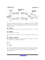
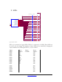
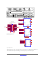
corresponding to one value of the highest nibble of the address. Hex addresses 0XXXXXXXX
are FPGA A, 1XXXXXXX are FPGA B and 2XXXXXXX are fpga C.)
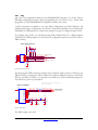
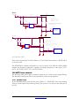
Some time after this, the FPGA should assert the DONE signal. This will allow the Spartan to
begin more transactions. The FPGA may delay this for up to 256 clock cycles before a timeout
is recorded and the transaction is cancelled.
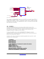
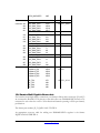
Main bus can be controlled from the USB Controller program. (Read and write single addresses,
or to/from files) It can also be written from the main.txt configuration method. The main.txt
syntax is
MAIN BUS 0x<addr> 0x<data>
Where <addr> and <data> are 8-digit (32-bit) hexadecimal numbers.
4 Compiling the Reference Design
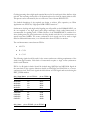
The MainTest reference design (for which bit files are included on the user CD and the
provided SmartMedia card) can be found on the user CD here.
D:\FPGA_Reference_Designs\
\common\DDR2\controller_ver\*
\ddr2_to_mb\*
\dn8000k10pci
\LVDS_intercon\source\*
The top module is
D:\FPGA_Reference_Designs\dn8000k10pci\LVDS_intercon\source\fpga.v
This module includes all of the other required sources and expects the directory structure found
on the CD. (The “LVDS_intercon directory is named that because the "LVDS" bitfiles also
found on the user CD and the "MainTest" bitfiles use the same source code with #define
statements to switch on and off features).
4.1.1
The Xilinx Embedded Development Kit (EDK)
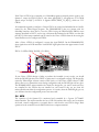
The reference design does not use the embedded PPC processors of the FX FPGA parts.
Therefore, EDK is not a required component of the reference design compilation.
4.1.2
Xinlinx XST
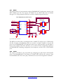
The Dini Group uses XST software to for design synthesis. The XST projects for each of the 3
FPGAs on the DN8000K10PCI can be found at ‘buildxst/*.xst’. These projects have been
compiled using XST version 9.1.
DN8000K10PCI User Guide
www.dinigroup.com
133