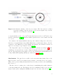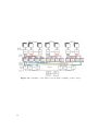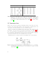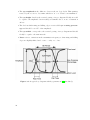
1
Department of Physics and Astronomy
University of Heidelberg
Bachelor Thesis in Physics
submitted by
Jens Kröger
born in Lübbecke (Germany)
2014
Data Transmission at High Rates
via Kapton Flexprints for the Mu3e Experiment
This Bachelor Thesis has been carried out by
Jens Kröger
at the
Physikalisches Institut Heidelberg
under the supervision of
Prof. Dr. André Schöning
Abstract
The Mu3e experiment is aiming to search for the neutrinoless muon decay µ+ → e+ e− e+
with a sensitivity of one in 1016 decays or better. This decay is lepton flavour violating
and strongly suppressed within the Standard Model. Therefore, even a single decay
signal would be a clear hint for new physics.
The concept of the Mu3e experiment is to achieve a very good momentum and time
resolution and an excellent vertex reconstruction to suppress background to a sufficient
level. Since the decay electrons have a low energy up to 53 MeV, multiple Coulomb
scattering is the dominating limiting factor for the momentum and vertex resolution.
Therefore, the material budget inside the detector region must be kept at a minimum.
To achieve this, pixel detectors with a thickness of only 50 µm will be used which
are carried by a Kapton foil support structure. The pixel detectors shall be linked to
front-end FPGAs via ultra-thin Kapton flexprints.
The production and performance tests of self-manufactured Kapton flexprints are
the main scope of this thesis. It has been shown that flexprints with a trace width of
120 µm and a trace separation of 110 µm can be manufactured reliably with a laser
platform available at the Heidelberg University. In addition, bit error rate tests have
been performed which resulted in bit error rates below O(10−15 ) for 17 parallel channels
at a transmission rate of 800 Mbit/s each. Moreover, eye diagrams have been analyzed
to understand which factors mainly affect the signal quality.
Zusammenfassung
Das Mu3e-Experiment hat zum Ziel, den neutrinolosen Myon-Zerfall µ+ → e+ e− e+ mit
einer Genauigkeit von einem in 1016 Zerfällen oder besser zu suchen. Dieser Zerfall ist
leptonzahlverletzend und damit im Standardmodell so stark unterdrückt, dass selbst
ein einziger gemessener Zerfall ein klarer Hinweis auf neue Physik wäre.
Das Konzept des Mu3e-Experiments ist es, eine sehr gute Impuls- und Zeitauflösung
und Vertexrekonstruktion zu erreichen, um den Untergrund ausreichend stark zu unterdrücken. Da die Zerfallselektronen eine niedrige Energie von bis zu 53 MeV haben, ist
hauptsächlich Coulomb-Vielfachstreuung der limitierende Faktor für die Impuls- und
Vertexauflösung. Deshalb soll innerhalb des Detektors so wenig Material wie möglich
verbaut werden. Um dies zu erreichen, sollen Pixeldetektoren mit einer Dicke von lediglich 50 µm verwendet werden, die von einer Struktur aus Kaptonfolie getragen werden.
Die Daten werden über ultradünne Kaptonflexprints zu Front-End FPGAs übertragen.
Die Herstellung sowie Performance-Tests selbsthergestellter Kapton-Flexprints sind
die Schwerpunkte dieser Arbeit. Es konnte gezeigt werden, dass Flexprints mit Leiterbahnbreiten von 120 µm und Abständen von 110 µm zuverlässig mit einer Laserplattform an der Universität Heidelberg hergestellt werden können. Zusätzlich sind
Fehlerraten-Tests durchgeführt worden, die Werte unter O(10−15 ) für 17 parallele Kanäle bei einer Datenrate von je 800 Mbit/s ergeben haben. Darüber hinaus sind Augendiagramme analysiert worden, um zu verstehen, welche Faktoren die Signalqualität im
Wesentlichen beeinflussen.
Contents
I
Theory & Background
1
1 Theoretical Background
1.1 The Standard Model . . . . . . .
1.1.1 The Elementary Particles
1.1.2 Muon Decays . . . . . . .
1.2 Experimental Situation . . . . .
.
.
.
.
.
.
.
.
.
.
.
.
.
.
.
.
.
.
.
.
.
.
.
.
.
.
.
.
.
.
.
.
.
.
.
.
.
.
.
.
.
.
.
.
.
.
.
.
.
.
.
.
.
.
.
.
.
.
.
.
.
.
.
.
.
.
.
.
.
.
.
.
.
.
.
.
.
.
.
.
.
.
.
.
.
.
.
.
2
2
2
3
4
2 The Mu3e Experiment
2.1 The Mu3e Experiment . . . .
2.1.1 The Signal Decay . . .
2.1.2 Background Decays .
2.1.3 Experimental Concept
2.1.4 The Readout Concept
2.1.5 The Muon Beam . . .
.
.
.
.
.
.
.
.
.
.
.
.
.
.
.
.
.
.
.
.
.
.
.
.
.
.
.
.
.
.
.
.
.
.
.
.
.
.
.
.
.
.
.
.
.
.
.
.
.
.
.
.
.
.
.
.
.
.
.
.
.
.
.
.
.
.
.
.
.
.
.
.
.
.
.
.
.
.
.
.
.
.
.
.
.
.
.
.
.
.
.
.
.
.
.
.
.
.
.
.
.
.
.
.
.
.
.
.
.
.
.
.
.
.
.
.
.
.
.
.
.
.
.
.
.
.
.
.
.
.
.
.
6
6
6
7
8
10
11
3 Basics of Data Transmission
3.1 Signals . . . . . . . . . . . . . . . . . . . .
3.1.1 Low Voltage Differential Signaling
3.1.2 Data Encoding . . . . . . . . . . .
3.2 Transmission Lines . . . . . . . . . . . . .
3.2.1 The Characteristic Impedance . .
3.2.2 Microstrips . . . . . . . . . . . . .
3.3 Signal Quality Checks . . . . . . . . . . .
3.3.1 Bit Error Rate Tests (BERTs) . .
3.3.2 Eye Diagrams . . . . . . . . . . . .
.
.
.
.
.
.
.
.
.
.
.
.
.
.
.
.
.
.
.
.
.
.
.
.
.
.
.
.
.
.
.
.
.
.
.
.
.
.
.
.
.
.
.
.
.
.
.
.
.
.
.
.
.
.
.
.
.
.
.
.
.
.
.
.
.
.
.
.
.
.
.
.
.
.
.
.
.
.
.
.
.
.
.
.
.
.
.
.
.
.
.
.
.
.
.
.
.
.
.
.
.
.
.
.
.
.
.
.
.
.
.
.
.
.
.
.
.
.
.
.
.
.
.
.
.
.
.
.
.
.
.
.
.
.
.
.
.
.
.
.
.
.
.
.
.
.
.
.
.
.
.
.
.
13
13
13
15
18
19
20
21
22
23
II
.
.
.
.
.
.
.
.
.
.
.
.
Measurements & Results
4 Manufacturing of Kapton Flexprints
4.1 The Laser Platform . . . . . . . .
4.2 Kapton . . . . . . . . . . . . . .
4.2.1 Physical Properties . . . .
4.2.2 Electrical Properties . . .
4.3 Aluminum . . . . . . . . . . . . .
4.4 Structure Sizes . . . . . . . . . .
4.4.1 Impedance Calculations .
25
.
.
.
.
.
.
.
.
.
.
.
.
.
.
.
.
.
.
.
.
.
.
.
.
.
.
.
.
.
.
.
.
.
.
.
.
.
.
.
.
.
.
.
.
.
.
.
.
.
.
.
.
.
.
.
.
.
.
.
.
.
.
.
.
.
.
.
.
.
.
.
.
.
.
.
.
.
.
.
.
.
.
.
.
.
.
.
.
.
.
.
.
.
.
.
.
.
.
.
.
.
.
.
.
.
.
.
.
.
.
.
.
.
.
.
.
.
.
.
.
.
.
.
.
.
.
.
.
.
.
.
.
.
.
.
.
.
.
.
.
.
.
.
.
.
.
.
.
.
.
.
.
.
.
26
26
27
27
27
29
30
30
4.5
4.4.2 Test Structures . . . . . .
Flexprint Cables . . . . . . . . .
4.5.1 Limitations . . . . . . . .
4.5.2 Obtaining Different Types
4.5.3 Mechanical Properties . .
4.5.4 Blackening of the Kapton
. . . . . . . . .
. . . . . . . . .
. . . . . . . . .
of Microstrips
. . . . . . . . .
. . . . . . . . .
5 Performance of BERTs
5.1 Hardware . . . . . . . . . . . . . . . . .
5.1.1 Field Programmable Gate Array
5.1.2 FPGA Development Board . . .
5.1.3 HSMC Flexprint Adapter Board
5.2 Software . . . . . . . . . . . . . . . . . .
5.2.1 Altera Quartus II . . . . . . . . .
5.2.2 ModelSim . . . . . . . . . . . . .
5.3 Firmware: BERT Implementation . . .
5.3.1 Data Generator . . . . . . . . . .
5.3.2 8b/10b Encoder . . . . . . . . .
5.3.3 LVDS Transmitter . . . . . . . .
5.3.4 LVDS Receiver . . . . . . . . . .
5.3.5 8b/10b Decoder . . . . . . . . .
5.3.6 Data Checker . . . . . . . . . . .
5.4 BERT Results . . . . . . . . . . . . . . .
.
.
.
.
.
.
.
.
.
.
.
.
.
.
.
.
.
.
.
.
.
.
.
.
.
.
.
.
.
.
.
.
.
.
.
.
.
.
.
.
.
.
.
.
.
.
.
.
.
.
.
.
.
.
.
.
.
.
.
.
.
.
.
.
.
.
.
.
.
.
.
.
.
.
.
.
.
.
31
34
35
37
38
39
.
.
.
.
.
.
.
.
.
.
.
.
.
.
.
.
.
.
.
.
.
.
.
.
.
.
.
.
.
.
.
.
.
.
.
.
.
.
.
.
.
.
.
.
.
.
.
.
.
.
.
.
.
.
.
.
.
.
.
.
.
.
.
.
.
.
.
.
.
.
.
.
.
.
.
.
.
.
.
.
.
.
.
.
.
.
.
.
.
.
.
.
.
.
.
.
.
.
.
.
.
.
.
.
.
42
43
43
43
43
45
45
46
46
46
47
47
47
47
48
49
6 Analysis of Eye Diagrams
6.1 Test Setup . . . . . . . . . . . . . . . . . . . . . . . . . . . . .
6.1.1 Tektronix DPO 7254C Digital Phosphor Oscilloscope .
6.1.2 Tektronix TDP3500 Differential Probe . . . . . . . . .
6.2 Eye Diagram Results . . . . . . . . . . . . . . . . . . . . . . .
6.2.1 Influence of the HSMC Flexprint Adapter Board . . .
6.2.2 Influence of the Cable Length . . . . . . . . . . . . . .
6.2.3 Influence of the Transmission Rate . . . . . . . . . . .
6.2.4 Influence of the Pre-Emphasis . . . . . . . . . . . . . .
6.2.5 Crosstalk between Trace Pairs . . . . . . . . . . . . .
6.2.6 Influence of the Microstrip Type . . . . . . . . . . . .
6.2.7 Influence of the Knee Length . . . . . . . . . . . . . .
.
.
.
.
.
.
.
.
.
.
.
.
.
.
.
.
.
.
.
.
.
.
.
.
.
.
.
.
.
.
.
.
.
.
.
.
.
.
.
.
.
.
.
.
.
.
.
.
.
.
.
.
.
.
.
.
.
.
.
.
.
.
.
.
.
.
51
51
52
52
53
53
56
59
60
61
62
64
.
.
.
.
.
.
.
.
.
.
.
.
.
.
.
.
.
.
.
.
.
.
.
.
.
.
.
.
.
.
.
.
.
.
.
.
.
.
.
.
.
.
.
.
.
.
.
.
.
.
.
.
.
.
.
.
.
.
.
.
.
.
.
.
.
.
.
.
.
.
.
.
.
.
.
.
.
.
.
.
.
.
.
.
.
.
.
.
.
.
.
.
.
.
.
.
.
.
.
.
.
.
.
.
.
.
.
.
.
.
.
.
.
.
.
.
.
.
.
.
.
.
.
.
.
.
.
.
.
.
.
.
.
.
.
.
.
.
.
.
.
.
.
.
.
.
.
.
.
.
.
.
.
.
.
.
.
.
.
.
.
.
.
.
.
III Conclusion & Outlook
7 Conclusion
7.1 Manufacturing of Kapton Flexprints
7.2 BERT Results . . . . . . . . . . . . .
7.3 Eye Diagram Results . . . . . . . . .
7.4 Recommendations . . . . . . . . . .
67
.
.
.
.
.
.
.
.
.
.
.
.
.
.
.
.
.
.
.
.
.
.
.
.
.
.
.
.
.
.
.
.
.
.
.
.
.
.
.
.
.
.
.
.
.
.
.
.
.
.
.
.
.
.
.
.
.
.
.
.
.
.
.
.
.
.
.
.
.
.
.
.
.
.
.
.
.
.
.
.
68
68
69
69
70
8 Outlook
8.1 Consequences for the Mu3e Experiment
8.1.1 Spatial Constraints . . . . . . . .
8.1.2 Transmission Errors . . . . . . .
8.2 Further Work . . . . . . . . . . . . . . .
.
.
.
.
.
.
.
.
.
.
.
.
.
.
.
.
.
.
.
.
.
.
.
.
.
.
.
.
.
.
.
.
.
.
.
.
.
.
.
.
.
.
.
.
.
.
.
.
.
.
.
.
.
.
.
.
.
.
.
.
.
.
.
.
.
.
.
.
.
.
.
.
71
71
71
72
73
List of Figures
74
List of Tables
75
Bibliography
76
Acknowledgements
80
Part I
Theory & Background
1 Theoretical Background
1.1 The Standard Model
1.1.1 The Elementary Particles
The Standard Model of particle physics (SM) [1] is a quantum field theory that comprises the description of the smallest constituents of matter, the elementary particles, as
well as the electromagnetic, the weak, and the strong interaction. Only gravity cannot
be described. The SM was developed throughout the second half of the 20th century
and has passed countless experimental tests until today. Especially the recent discovery
of a new particle, which is likely to be the long predicted Higgs boson, has given further
support to this theory [2, 3].
According to the SM, the fundamental particles comprise six quarks, six leptons, and
their corresponding anti-particles. Furthermore, there are four types of gauge bosons
and the Higgs boson (see Figure 1.1). The quarks and leptons form three generations.
The first generation contains the up quark (u) and the down quark (d) with charges of
+2/3 and -1/3 in units of the elementary charge, the electron (e− ) and the electrically
neutral electron neutrino (νe ).
The second and the third generation are also made up of a pair of quarks, a lepton
and a neutrino. These are the charm quark (c) and the strange quark (s) together with
the muon (µ− ) and the muon neutrino (νµ ) in the second generation and the top quark
(t), the bottom quark (b) together with the tau (τ ) and the tau neutrino (ντ ) in the
third generation.
All quarks and leptons are spin 1/2 particles, i.e. they are fermions. The interaction
between them is mediated by the gauge bosons which have spin 1. The eight gluons
are responsible for the strong interaction, the photon (γ) mediates the electromagnetic
force and the Z0 , W+ and W− go with the weak interaction.
In the SM, the neutrinos are considered to be massless. The so-called lepton flavour
number, i.e. the number of anti-leptons subtracted from the number of leptons of one
generation, is a conserved quantity.
2
Figure 1.1: Particles described by the SM [4].
In spite of the great successes of the SM, observations have been made which cannot
be explained by this theory. Several experiments have observed neutrino oscillation,
such as Super-Kamiokande [5], SNO [6], KamLAND [7], and Daya-Bay [8]. To explain this mixing of the flavour eigenstates, the neutrinos need a non-vanishing mass,
which is not foreseen in the SM. An extension by heavy right-handed neutrinos, called
νSM, yields consistent results with oscillation experiments [9]. Still it cannot be explained why the neutrino masses are orders of magnitude smaller than those of the other
particles. Moreover, νSM does not provide any explanation for the observed matterantimatter-asymmetry, the origin of dark matter, or the existence three generations
of particles. These phenomena motivate theories beyond the Standard Model (BSM),
such as supersymmetric theories (SUSY). In contrast to the SM, many of these predict
flavour violating processes at an observable branching ratio.
1.1.2 Muon Decays
(Anti-)muons are unstable and have a mean lifetime of about 2.2 µs. The dominating decay in the SM is µ+ → e+ νe ν̄µ [1]. Considering neutrino mixing (and therefore
allowing lepton flavour violation) the muon decay can also be realised without outgoing
neutrinos (see Figure 1.2b).
3
(a) Dominant SM muon decay: the Michel
decay.
(b) Strongly suppressed decay µ+ → e+ e+ e−
with neutrino oscillation.
Figure 1.2: Feynman diagrams of possible SM muon decays [10].
As the W+ mass of 80.4 GeV/c2 is much higher than the neutrino mass differences
(< 2 eV) [1], the decay µ+ → e+ e− e+ is strongly suppressed with a branching ratio
(BR) below 10−54 [11] and thus unobservable.
There are BSM theories that predict a much higher BR for this decay introducing
new tree couplings (see Figure 1.3a) or loop contributions with new particles (see Figure
1.3b). Therefore, any observation of this process would be a clear hint for new physics.
(a) Tree diagram involving an
unknown particle X.
(b) Penguin diagram with a SUSY
loop.
Figure 1.3: Feynman diagrams of possible BMS muon decays [10].
1.2 Experimental Situation
Since 1953 experiments are performed to search for lepton flavour violation in muon
decays (see Figure 1.4) [11–13]. Until today only upper limits for the branching ratios
were found. The current upper limit for the µ+ → e+ e+ e− decay is set by the SINDRUM experiment [14], whereas the best measurement for µ+ → e+ γ was performed
by the MEG experiment [15].
4
SINDRUM
From 1983-86, the SINDRUM experiment was in operation at the Paul-Scherrer-Institut
(PSI) in Villigen, Switzerland. Because no signal event was detected, an upper limit for
the branching ratio BR(µ+ → e+ e+ e− ) < 10−12 could be set at 90% confidence level
(CL) [14].
In the experiment, which was placed inside a solenoid magnetic field of 0.33 T, muons
with a momentum of about 28 MeV/c were stopped in a hollow double-cone target.
The decay products were measured by five tracking layers of multiwire proportional
chambers and an array of scintillators for triggering and timing measurements.
MEG
To search for the LFV decay µ+ → e+ γ the MEG experiment uses a drift chamber to
detect the positron and a liquid xenon calorimeter for the photon. It has been running
at PSI since 2008 and is currently being upgraded to MEG II [16]. The current upper
limit is BR(µ+ → e+ γ) < 5.7 · 10−13 at 90% CL [15].
Figure 1.4: The history of LFV muon decay experiments, adapted from [11].
5
2 The Mu3e Experiment
2.1 The Mu3e Experiment
Mu3e is an experiment to search for the lepton flavour violating decay µ+ → e+ e+ e− [17].
It is aiming to be sensitive for better than one signal decay in 1016 muon decays. This
would increase the sensitivity by four orders of magnitude compared to the current
upper limit given by SINDRUM.
To perform the experiment on a reasonable time scale, a very high muon stopping rate
of O(109 /s) is needed. Consequently, the main challenges for the detector design are to
handle high data rates and to have a very efficient accidental background suppression.
For the latter, a very precise vertex fitting < 200 µm as well as a momentum resolution
below 0.5 MeV/c and an excellent time resolution < 100 ps are needed.
The main limiting factors for the momentum and vertex resolution is multiple Coulomb
scattering of the decay electrons in the detector material. Thus, the material budget of
the detector must be as low as possible.
2.1.1 The Signal Decay
The muons will be stopped in a target to decay at rest. Thus the total momentum of
the decay electrons is vanishing:
p~tot =
3
X
p~i = 0.
(2.1)
i=1
The decay at rest constrains the total energy to be equal to the rest mass of the
muon:
Etot =
3
X
Ei = mµ · c2 ≈ 105.7 MeV.
(2.2)
i=1
In summary, the signal decay is given by three electrons with a vanishing total momentum and an energy between me c2 ≈ 0.5 MeV and 1/2 · mµ ≈ 53 MeV coming from
a common vertex and being coincident in time.
6
2.1.2 Background Decays
Any background is due to fake signals that can be divided into two groups: internal
conversion and random combinatorial background.
Internal Conversion
Internal conversion is the decay µ+ → e+ e− e+ νe ν̄µ (see Figure 2.1) which has a branching ratio of 3.4 · 10−5 [1]. Here, the emitted photon immediately converts into an
electron-positron pair.
Considering vertex and timing, this decay is indistinguishable from the signal decay.
The only difference is a fraction of momentum and energy carried away by the neutrinos
which cannot be detected. This clarifies the need for a very high momentum resolution.
If both neutrinos have a vanishing momentum, this decay looks exactly as the signal
decay. This is the only irreducible background.
In Figure 2.2, the branching ratio for the internal conversion as a function of the
missing energy is plotted. The missing energy corresponds to the difference of mµ · c2
and the energy carried away by the electrons which is measured. To suppress this
background sufficiently, an energy resolution below 1 MeV is needed.
Figure 2.1: The internal conversion decay
µ+ → e+ e− e+ νe ν̄µ [18].
Figure 2.2: Branching ratio for the
internal conversion as a function
of the missing energy [19].
Random Combinatorial Background
Due to a limited spatial resolution two nearby vertices cannot be properly separated if
they are too close together.
As can be seen in Figure 2.3a two positrons from the dominant Michel decay µ+ →
e+ νe ν̄µ (see Figure 1.2a) can be accidentally combined with an electron, for example produced by photon conversion or Bhabha scattering. Another possibility is the
7
(a) Accidental combination of two Michel
positrons with an electron from pair
production.
(b) Accidental combination of an
electron-positron pair from internal
conversion with a Michel positron.
Figure 2.3: Possible combinatorial background.
combination of an electron and a positron from the internal conversion process µ+ →
e+ e− e+ νe ν̄µ with a Michel positron (see Figure 2.3b).
2.1.3 Experimental Concept
As discussed above, for an efficient background suppression high rate capabilities as
well as excellent spatial, time and momentum resolution are crucial.
The basic concept of the Mu3e experiment is to measure the momenta of the muon
decay electrons in a solenoidal magnetic field of 1 T with a silicon pixel detector.
Because multiple Coulomb scattering in the detector material is the limiting factor
h of radiation
for the momentum resolution, minimizing the material budget below 1
length per layer in the active detector region is essential.
In Figure 2.4 a schematic view of the detector design is shown. The incoming muon
beam will be stopped in a hollow double-cone made of aluminum to decay at rest. Four
layers of very thin pixel detectors are arranged in two double layers (black) to track
the decay electrons. Furthermore, scintillating fibres (grey) are used for precise timing
measurements. As the experiment is placed in a magnetic field, the electrons are curled
back and detected again by another double layer of pixel sensors. Finally, they are
stopped in scintillating tiles which again yield precise timing information.
Pixel Detector The Mu3e pixel detector consists of High-Voltage Monolithic Active
Pixel Sensors (HV-MAPS) with a pixel size of 80×80 µm2 . The chips are thinned down
8
Figure 2.4: Schematic drawing of the detector design. The blue and the red lines
represent recurling positrons and an electron from a signal decay. On the
right side: view along the beam axis [17].
to 50 µm and have a size of 1 × 2 cm2 in the inner layers, and 2 × 2 cm2 in the outer
and the recurl layers [20, 21]. With 275 million pixels an area of more than 1 m2 will
be covered.
In contrast to the classical MAPS technology, the ionization charges are collected by
drift due to an applied high voltage (HV). This leads to a much faster charge collection
compared to the diffusion process in MAPS. In addition, the radiation tolerance is
improved. Several prototype chips are tested [22–24].
The chips will be glued on a self-supporting Kapton structure (see Figure 2.5) with
a thickness of 25 µm and wire bonded to Kapton flexprint cables for power supply and
readout. The triggerless readout will be done by zero-suppressed serial 800 Mbit/s Low
Voltage Differential Signaling (LVDS) (see Subsection 3.1.1) [25–27].
Fibre Detector
The pixel detector will be read out in 50 ns time frames. Due to the
high decay rate of 2·109 /s about 100 decays per frame occur in the detector acceptance.
Thus, a more precise timing measurement is needed and provided by the scintillating
fibre detector.
The fibre detector consists of two or three layers of scintillating fibres with a diameter
of 250 µm forming ribbons. The light produced by scintillation will be read out with
arrays of silicon photo-multipliers (SiPM) mounted at both ends of the ribbons [28].
9
Figure 2.5: First mechanical prototype of the Kapton support structure for the inner
two layers (length: 12 cm).
Tile Detector
7.5 × 5
mm3
The third sub-detector is a scintillating detector consisting of 7.5 ×
tiles which are also read out by SiPMs. It will be placed right underneath
the recurl pixel double-layer.
As this is the last measurement of the decay particles more material can be used.
This leads to a detection efficiency close to 100% and a very high timing accuracy below
100 ps [29].
Detector Environment As mentioned above, the whole detector will be placed in
a solenoidal homogeneous magnetic field of 1 T to bend the electron tracks. The
front-end electronics will be placed directly on the muon beam pipe. For cooling, the
whole detector volume will be filled with a circulating helium atmosphere. In addition,
channels in the Kapton support structure will be flushed with gaseous helium for cooling
of the pixel detectors [30–32].
2.1.4 The Readout Concept
In Figure 2.6, a schematic of the Mu3e readout chain is shown. The pixel sensors as
well as the fibre and tile detectors will be connected to so-called front-end FPGAs (field
programmable gate arrays, see Subsection 5.1.1). These FPGAs will be located directly
on the beam pipe inside the detector.
10
The connection between the pixel detectors and the front-end FPGAs will be realized
by serial 800 Mbit/s LVDS links (low voltage differential signalling, see Subsection 3.1.1)
which will consist of tiny aluminum traces on Kapton. The manufacturing and performance tests of these so-called flexprints are the main scope of this work (see Chapter 4).
From the front-end FPGAs, the data will be sent out from the detector to FPGAdriven readout boards via high-speed optical links. Thus, a galvanic separation is
guaranteed.
The data from the readout boards will then be transmitted via high-speed optical
links to a GPU (graphical processing unit) filter farm where an online track and event
reconstruction will be performed. Events of interest will then be sent to a data collection
server which stores them in a mass storage system.
2.1.5 The Muon Beam
As an extremely high number of muons needs to be stopped to decay, a very intense
muon beam is required. Therefore, the Mu3e experiment is supposed to be run at the
Paul-Scherrer-Institut (PSI) in Switzerland, which operates the world’s most intense
muon source.
The PSI operates a cyclotron to accelerate protons which hit a carbon target, where
pions are created as secondary particles. Slow pions decay immediately into muons
which are collected in the πE5 beamline so that a low momentum muon beam with a
rate of 2 · 108 1/s is provided for a first phase of the Mu3e experiment.
In a second phase, the Mu3e experiment aims to improve the sensitivity by another
order of magnitude. Therefore, a more intense muon beam is needed. Such a beam
could be provided by the planned High intensity Muon Beamline (HiMB) for which
the protons from the cyclotron mentioned above will be shot on the Swiss Spallation
Neutron Source (SINQ) target [33]. There, a high number of muons will be created as
a by-product and could be collected by the HiMB to provide a muon rate of 2 · 109 1/s.
11
Figure 2.6: Schematic of the Mu3e readout chain consisting of three stages.
12
3 Basics of Data Transmission
Data transmission is the transport of information from one point to another whereby
the data is represented by a physical signal [34].
3.1 Signals
A signal is the time-dependent magnitude of an observable. Electrical signals can be
represented by a voltage or current. Also electromagnetic waves (optical or radio) can
be used. To have an effective content of information, the time evolution of the signal
must be unpredictable because otherwise the receiver can foresee incoming data which
makes the transmission redundant [35].
Analogue Signals
An analogue signal is continuous in time and amplitude. In principle, every classical
physical observable like brightness, temperature, or pressure can be understood as an
analogue signal. Mathematically, it can be described by a smooth function of time [36].
Digital Signals
On the contrary, a digital signal consists of a sequence of discrete values. That is to
say, there is only a limited set of well distinguishable values which can be attained
and which are furthermore only defined at periodic points in time. An analogue signal
can be transformed into a digital signal by quantisation and sampling in constant time
intervals [36].
In electronics, it is common to use merely the two Boolean values 0 (false) and 1
(true) which are associated to two logic voltage levels or the transitions between those.
The binary numeral system provides the theoretical basis to use binary codes (sequences
of zeros and ones) for digital information processing of all kinds.
3.1.1 Low Voltage Differential Signaling
Low Voltage Differential Signaling (LVDS) is an interface standard for high-speed
data transmission. It describes the physical layer which means that it only comprises
13
Figure 3.1: Schematic drawing of a basic LVDS circuit. Also, the field coupling of the
differential pair is shown [38].
the mechanical and electronic components, i.e. the hardware, of a physical link but no
encoding schemes or protocols [37].
Figure 3.1 shows the architecture of an LVDS link. A current source is injecting a
constant current of 3.5 mA into the circuit. Transistors work as switches to control
the direction of the current towards the receiver. At the receiver side, there is a 100 Ω
terminating resistor at which a voltage of 350 mV drops according to Ohm’s law.
The receiver, which is a comparator with a transition threshold of about 50 mV,
senses the polarity of the signal to determine the logic state being transmitted.
LVDS has the advantage of generating very low electromagnetic noise due to the
closely coupled wires. As they carry the same current in opposite directions, most of
the radiation is cancelled. For the same reason, an LVDS link is relatively insensitive
to external electromagnetic noise because the noise will nearly equally affect both wires
and cancel out. This means that there is only very little cross-talk between adjacent
wire pairs even if they are close to each other.
Another considerable advantage of LVDS is the low power consumption because of
the low voltage and little radiative losses compared to other concepts of signaling. The
power consumption is particularly low if it can be ensured by the transmitter side that
there is no disparity, i.e. the number of ones equals the number of zeros transmitted,
because in this case there is not even a net current averaged over time (see 8b/10b
encoding below).
14
Figure 3.2: A binary datastream and the corresponding voltage dropping across the
terminating resistor [39].
An LVDS connection is a serial link which means that the data is transmitted bit
after bit and not in parallel (except when using several LVDS links in parallel). In
Figure 3.2, an arbitrary binary datastream and the corresponding voltage levels are
shown.
3.1.2 Data Encoding
Encoding is an injective mapping to transform data, i.e. a series of logic states, into
a pattern suitable for transmission. The purpose of so-called line codes is to specify
how the bit states ’0’ and ’1’ are represented in a signal. Because different transmission
media have different properties, there are several schemes to match these characteristics.
The simplest possible code is the non-return-to-zero code (NRZ) (see Figure 3.3a).
Ones and zeros are represented by two distinct logic levels of the signal and form a continuous sequence. Using this code can cause problems if a long sequence of subsequent
ones or zeros is transmitted because in this case the logic level remains constant over a
long period so that the synchronization with the underlying clock can be lost [40].
Another line code is the Manchester code in which falling and rising edges, i.e. the
transitions between the two logic levels, represent ones and zeros, respectively. With
this code clock recovery (see below) is relatively easy due to frequent transitions. A
disadvantage is that twice the bandwidth compared to NRZ is required to be able to
send subsequent ones or zeros (see Figure 3.3b) [42].
Line codes are not only used to specify how ones and zeros are represented in a signal.
They also provide schemes how to encode bit words of a certain length in a bit pattern
15
(a) The non-return-to-zero code: ones and (b) The Manchester code: ones and zeros are
zeros are represented by two logic levels of the
represented by falling and rising edges
signal.
respectively.
Figure 3.3: The bit pattern ”11011000100” represented in two commonly used line
codes: the NRZ and the Manchester code [41].
with properties suiting the physical link [43]. Furthermore, additional information can
be contained for the following purposes:
• If there is no extra clock transmission line sending ”0101...” continuously, the clock
has to be recovered from the data stream (clock recovery). Therefore a high
transition rate between the logic levels is favourable.
• Some encoding schemes provide the possibility to send either data or a predefined
control sequence of bits. If transmitting a continuous bit stream, control words
can be used to identify bit packets (words). Thus, the bit stream can be cut into
words of a certain length.
• For some physical layers, like LVDS, it is desirable to have DC balance, i.e. to
send an equal number of ones and zeros to achieve a vanishing net current. By
an encoding scheme like 8b/10b this can be accomplished.
• A detection of transmission errors is possible if bit patterns are used for
which a single bitflip yields an invalid word.
8b/10b Encoding
The disparity (dp) of a bit pattern is given by the difference in number of ones and
zeros, counting ones as -1/2 and zeros as 1/2. If considering a continuous data stream,
the running disparity (rd) is defined as the running sum over all previously transmitted words.
For 8 bit words encoded in 10 bits it is possible to ensure DC balance in a long run.
That is because with 8 bits 28 = 256 words can be created, whereas with 10 bits there
are 210 = 1024 combinations. Regarding the restrictions that the 10 bit patterns shall
16
Word
Data
dp=-1
dp=+1
Word
Data
dp=-1
dp=+1
D.00
D.01
D.02
D.03
D.04
D.05
D.06
D.07
D.08
D.09
D.10
D.11
D.12
D.13
D.14
D.15
00000
00001
00010
00011
00100
00101
00110
00111
01000
01001
01010
01011
01100
01101
01110
01111
100111 011000
011101 100010
101101 010010
110001
110101 001010
101001
011001
111000 000111
110001 000110
100101
010101
110100
001101
101100
011100
01011 101000
D.16
D.17
D.18
D.19
D.20
D.21
D.22
D.23
D.24
D.25
D.26
D.27
D.28
D.29
D.30
D.31
10000
10000
01010
01011
01100
01101
01110
10111
11000
11001
11010
11011
11100
11101
11110
11111
011011 100100
100011
010011
110010
001011
101010
011010
111010 000101
110011 001100
100110
010110
110110 001001
001110
101110 010001
011110 100001
101011 010100
K.28
11100
001111
110000
Table 3.1: 5b/6b encoding scheme. For several 5 bit words two different patterns with
disparity dp = ±1 exist. D.x mark the 25 = 32 possible data words, K.28 is a
control word [26].
suffice a disparity of 0 or ±2 and never have more than five equal subsequent bits, 584
of the possible 1024 combinations are left.
One way of implementing this concept has been developed by IBM in 1983 [44]. The
8 bits of a word are split into two parts and are treated separately according to an 5b/6b
and an 3b/4b part (see Tables 3.1 and 3.2), respectively. During the data transmission,
the running disparity is determined to control the combination of 6 bits and 4 bits being
used to satisfy the condition dp = 0 or dp = ±1.
Besides the advantage of DC balancing, this encoding scheme comprises some control
words (so-called K-words) which do not encode data but can be used for clock recovery
and phase alignment before beginning to transmit user data or to bypass phases when
no actual data is transmitted to retain the synchronization. The K.28.7 word is of
particular importance because it does not result from a single bit flip in the data
stream.
17
Word
Data
dp=-1
D.x.0
D.x.1
D.x.2
D.x.3
D.x.4
D.x.5
D.x.6
D.x.P7
D.x.A7
000
001
010
011
100
101
110
111
111
1011
dp=+1
0100
1001
0101
1100
0011
1101
0010
1010
0110
1110
0001
0111
1000
K-Word
Data
dp=-1
dp=+1
K.x.0
K.x.1
K.x.2
K.x.3
K.x.4
K.x.5
K.x.6
K.x.7
000
001
010
011
100
101
110
111
1011
0110
1010
1100
1101
0101
1001
0111
0100
1001
0101
0011
0010
1010
0110
1000
Table 3.2: 3b/4b encoding scheme. For several 2 bit words two different patterns with
disparity dp = ±1 exist. For D.x.7 either P7 or A7 is used to ensure that in
the resulting 10 bit pattern never more than five equal bits occur. The K.x.y
words can be combined with the K.28 word of Table 3.1 to form a control
word [26].
3.2 Transmission Lines
Only for direct and very low frequency alternating currents, electric wires can be characterized solely by their ohmic resistance. If the wavelength of a signal is in the order
of the length of the link, this simple model is not sufficient any more.
Instead, a description as a transmission line is appropriate. This comprises not only
the resistance of the wire but also its capacitance and inductance (see Figure 3.4). In
place of the total resistance R, the inductivity L and the capacitance C their normalized
(i.e. per length dx) counterparts R0 , L0 and C 0 are used. G0 represents the conductance
of the dielectric material between the transmission line and ground.
Within this model, a real wire is described as an infinite series of such elements.
Figure 3.4: Equivalent circuit diagram of an infinitesimally short piece of a transmission line with normalized inductance L0 and resistance R0 coupled to ground
via G0 and C 0 [45].
18
3.2.1 The Characteristic Impedance
If the transmission line is homogeneous along its length, a single parameter is sufficient
to describe its behaviour: the characteristic impedance Z0 . It is equal to the ratio
of the complex voltage and the complex current of a wave travelling along the line.
It can be shown (see [46]) that Z0 is given by
s
Z0 =
R0 + iωL0
.
G0 + iωC 0
(3.1)
Note that Z0 is independent of the length of the transmission line. For an ideal
conducting material (R0 = 0) and an ideal dielectric (G0 = 0) or high frequencies
(R0 iωL0 and G0 iωC 0 ) equation 3.1 reduces to
s
Z0 =
L0
,
C0
(3.2)
so that the characteristic impedance is also independent of the frequency. In such
cases, Z0 is not related to the ohmic resistance of a wire which causes an attenuation of
the amplitude of a transmitted signal and is self-evidently dependent on the length of
the transmission line. The characteristic impedance is merely a parameter to describe
a wire’s high-frequency behaviour.
When considering a pair of transmission lines with opposite current, which is the case
for LVDS, another quantity is of importance: the differential impedance Zdiff . It is
defined as the ratio of the differential voltage Vdiff and the current I1 on one line [47].
Due to an inductive coupling between the lines, a current I1 in one trace will cause
a current α · I1 in the second trace with α ∈ (0, 1) being the coupling constant. A
calculation, which can be found in [48], yields
Zdiff = 2Z0 (1 − α) .
(3.3)
The differential impedance is of particular importance for reflections which occur if
wires or other electric components with different characteristic impedances are connected. The reflection coefficient Γ is given by
Γ=
Zdiff,b − Zdiff,a
,
Zdiff,a + Zdiff,b
(3.4)
where Zdiff,a and Zdiff,b correspond to two arbitrary connected components and Zdiff = R
in case of an ohmic terminating resistor. Γ is in the range of -1 to 1 and negative values correspond to a reflection with a phase shift by π. Obviously, the characteristic
19
impedance of all components of an electric circuit should be matched as good as possible to ensure proper signal propagation and minimize reflections [49].
3.2.2 Microstrips
Microstrips are a certain type of transmission lines which are commonly used on printed
circuit boards (PCBs) and flexprint cables (see Chapter 4). They are suited for signals
in the microwave range (300 MHz to 300 GHz).
Differential Microstips
A microstrip consists of a conducting trace which is separated from a ground (or other
constant potential) plane by a dielectric layer called substrate. For LVDS links (see
Subsection 3.1.1) a pair of wires is needed. When designing a PCB, the trace width w,
the trace separation s, the trace thickness t, and the dielectric thickness h, as well as the
dielectric constant of the substrate r (see Figure 3.5a) need to be taken into account
to match the impedance to the other electric components for minimal reflections.
Therefore, the following equation can be used for differential microstrips [50]. This
approximation is valid for ratios of w/h between 0.1 and 3.0.
s
174
5.98 · h
Zdiff = √
)(1 − 0.48 · e−0.96 h )
ln (
0.8 · w + t
r + 1.14
(a) Differential microstrips.
(3.5)
(b) Coplanar striplines.
Figure 3.5: Profiles of two kinds of microstrips.
Coplanar Striplines
At first appearance, coplanar striplines seem to be very similar to differential microstrips
(see Figure 3.5b), but there is a crucial difference when calculating the characteristic
impedance. This is because in case of the latter, there is a clear boundary condition for
the electric field surrounding the conducting traces due to the ground plane. According
to [51], the impedance Z0 of a coplanar stripline can be calculated by
120π K(k0 )
,
Z0 = √
eff K(k00 )
20
(3.6)
where eff is an effective dielectric constant given by
eff = 1 + (r − 1) ·
1 K(k 0 ) K(k0 )
2 K(k) K(k00 )
(3.7)
with K(•) being the elliptic integral of first kind and
k0 =
k=
s/2
,
s/2 + w
πs
tanh 4h
tanh π w+s/2
2h
,
k00 =
q
k0 =
p
1 − k02 ,
(3.8)
1 − k2 .
(3.9)
For practical purposes, α ≈ 0 and therefore Zdiff ≈ 2Z0 is assumed for coplanar
striplines within the scope of this thesis.
Typically, PCBs and flexprints with (differential) microstrips are produced in lithographic processes consisting of many steps in which multiple substrate and copper layers
are assembled. An overview of typical dimensions of microstrips in standard and leading
edge processes is given in Table 3.3.
copper thickness t
trace width w
trace separation s
dielectric thickness h
Multilayer PCB
(standard process) [52]
≥ 50 µm
≥ 100 µm
≥ 100 µm
≥ 60 µm
Multilayer PCB
(advanced process) [52]
approx. 25 − 30 µm
≥ 75 µm
≥ 75 µm
≥ 60 µm
Flexprint
(leading edge) [53]
≥ 5 µm
≥ 20 µm
≥ 25 µm
≥ 25 µm
Table 3.3: Typical parameters for microstrips on PCBs and flexprints.
3.3 Signal Quality Checks
Once a physical link has been realized, it needs to be tested to ascertain how reliable
data can be transmitted. There are mainly two concepts which will be introduced in
the following.
21
3.3.1 Bit Error Rate Tests (BERTs)
A bit error rate test (BERT) is a method to determine the quality of a transmission
link for digital data transmission. The bit error rate (BER) is the ratio of the number
of wrongly transmitted bits k and the total number of transmitted bits n and represents
an estimation for the probability p for an error to occur if one bit is transmitted:
BER = p =
# error bits
k
=
# total bits
n
(3.10)
In principle, a BERT can be realized by sending a deterministic datastream and comparing the incoming bits to the expected pattern at the receiver side [25]. The exact
architecture of the BERT used for this thesis is described in Chapter 5.
Mathematically, a BERT can be understood as a classical counting experiment. As
for every transmitted bit there are two discrete results (false or correct), it obeys a
binomial distribution. For data transmission at high rates, n becomes large within
seconds and the probability p for an error bit should be very small (p 1) due to a good
physical link. Therefore, the binomial distribution converges to a Poisson distribution
if µ := lim p · n > 0 and the probability P (k) to find k error bits in a large number of
n→∞
transmitted bits is given by
P (k) =
µk −µ
·e .
k!
(3.11)
For large n, the Poisson distribution converges to a normal distribution so that the
√
standard deviation is given by σk = k. Thus, for the BER one gets
√
k
k
BER = ±
.
n
n
(3.12)
Upper BER Limit
If no error is detected, i.e. k = 0, an estimation for an upper limit of the BER must
be found. In the following, a perfectly working data checker is assumed so that no
error counts occur accidentally, i.e. there is no background, and no error is overlooked.
According to [54] and [55], a Bayesian approach with a flat prior distribution is used.
Assuming a Poisson distribution and not observing any error bits (kobs = 0), from [55]
1 − CL =
one arrives at
22
kX
obs
pk · e−p
= e−p ,
k!
k=0
(3.13)
BER ≤
log(−CL)
2.996
≈
at 95% CL,
N
N
(3.14)
where CL is the confidence level.
3.3.2 Eye Diagrams
Eye diagrams allow to visualize and determine the quality of a transmitted digital signal
easily and quickly [56]. An eye diagram is constructed from a digital data-stream by
superimposing the waveform of an arbitrary bit stream in a single diagram with time
on the horizontal and signal amplitude on the vertical axis. Therefore, it represents the
average statistics of the signal.
An ideal waveform of the digital signal would result in a square-shaped eye diagram
as can be seen in Figure 3.6a. Due to impairments of the signal like attenuation, crosstalk or noise and a limited bandwidth of the transmitter, real physical signals differ
from this and rather resemble the eye diagram shown in Figure 3.6b. Here, the unit
interval UI is defined as the time it takes to transmit one bit and corresponds to the
inverse of the transmission rate.
(a) Ideal high-speed digital signal with eye
diagram.
(b) Typical example of a real high-speed
digital signal with eye diagram.
Figure 3.6: An ideal and a real arbitrary digital datastream superimposed in eye diagrams [56].
From an eye diagram a number of key parameters can be determined. These are
shown in Figure 3.7 and described in detail below.
• The zero-level and the one-level are the mean values of the lower and upper
logic levels, respectively. In NRZ coding they correspond to a ’0’ and a ’1’.
23
• The eye amplitude is the difference between the two logic levels. This quantity
is used by the receiver to determine whether a ’0’ or a ’1’ has been transmitted.
• The eye height describes the vertical opening of an eye diagram. Ideally, it would
be equal to the amplitude but in reality, it is smaller due to noise or saturation
effects.
• The level at which rising and falling edges cross is called eye crossing percentage and should be at 50% of the amplitude.
• The eye width corresponds to the vertical opening of an eye diagram and should
ideally be equal to the unit interval.
• Jitter refers to variations in the transmission frequency so that rising and falling
edges are slightly shifted and occur too early or too late.
Figure 3.7: A typical eye diagram with key parameters [56] (modified).
24
Part II
Measurements & Results
4 Manufacturing of Kapton Flexprints
A flexprint is a bendable plastic film carrying conducting traces which consist of copper
or aluminum. To manufacture flexprints, usually lithographic processes are used which
resemble those for PCB production. For this thesis, it was examined in what way
Kapton foils laminated with aluminum can be processed with a laser such that the
aluminum evaporates in some areas whereas the Kapton is damaged as little as possible
and conducting traces remain.
4.1 The Laser Platform
For manufacturing the flexprints, a PLS6MW Multi-Wavelength Laser Platform from
Universal Laser Systems (see Figure 4.1) has been used. It provides a plane work area
of approximately 80 × 46 cm2 on which a broad spectrum of materials can be processed
with different wavelengths as the laser source can be changed. For this thesis, a CO2
laser with a wavelength of 9.3 µm and a fibre laser with a wavelength of 1.06 µm are
available.
Figure 4.1: A photo of the PLS6MW Laser Platform, taken from [57].
For processing, a material is placed on the work area and scanned with the pulsed
laser. For ideal results, several parameters can be adjusted, such as laser power, laser
movement velocity, pulse frequency, waveform, and vertical focus position. The laser
can either treat areas (called ’rastering’) by moving back and forth in x-direction while
scanning the y-direction incrementally, or move along lines (called ’vectoring’). When
26
’rastering’, the additional parameters contrast, definition and density are adjustable.
In order to blow away evaporated material and prevent the lens from being contaminated with debris, a nozzle points an air stream onto the focus of the laser. Apart from
compressed air, every other gas can be used if not flammable. As light materials, such
as Kapton foils, can ripple or might even be blown away by the air stream, they should
be adhered to a sticky rubber mat.
Layouts must be designed as vector graphics with a third-party graphic software,
R
such as CorelDRAW
, and different laser settings can be assigned to the RGB-encoded
colors black, red, green, yellow, blue, magenta, cyan, and orange. The laser platform is
then addressed by the Windows Print System like an arbitrary printer [58].
4.2 Kapton
TM
R
Kapton
is a multi-purpose polyimide film developed by DuPont . It has an excellent
balance of electrical, thermal, mechanical, physical, and chemical properties and was
used in applications with a wide temperature range from −269◦ C up to 400◦ C [59].
Furthermore, it can be laminated with a thin metal layer or glued to another film of
Kapton. For the Mu3e experiment 25 µm Kapton Type HN is planned to be used for
flexprints and the mechanical support structure to minimize the material budget inside
the active detector region.
4.2.1 Physical Properties
Kapton is mechanically stable though flexible and retains its physical properties over a
wide temperature range. It does not melt or burn and has the highest UL-94 flammability rating: V-0 [60].
Between 360◦ C and 410◦ C a second order phase transition occurs which is assumed to
be a glass transition. According to the manufacturer, different measurement techniques
result in different transition temperatures [60].
4.2.2 Electrical Properties
The dielectric constant r of Kapton depends on the relative humidity of the air as
well as on the temperature and the frequency. In Figure 4.2, r is plotted versus these
quantities. Assuming normal conditions and a relative humidity around 50%, r is
approximately 3.4.
27
(a) r vs. rel. humidity at room temperature,
type HN film, 25 µm.
(c) r vs. frequency at various temperatures, type HN,
25 µm.
(b) r vs. temperature for two frequencies,
type HN, 25 µm.
(d) r vs. frequency at 25◦ C and 45%
rel. humidity, type HN, 125 µm. B
corresponds to the same measurement as A
after conditioning the film at 100◦ C for 48 h.
Figure 4.2: Dependence of the dielectric constant r on various quantities,
from [60] (modified).
28
4.3 Aluminum
Though aluminum has only 63% of the electrical conductivity of copper and a lower
heat conductivity [61], it is widely used in electronic applications due to its low mass
density and easy processing [62, 63].
It also has a much lower atomic number Z than copper which makes it particularly
interesting for the Mu3e experiment because of the multiple scattering dominated electron interactions with matter. According to [64], multiple scattering can be quantified
by ΘM S being the root mean square (RMS) of the central 98% of the planar scattering
contribution. It is given by
ΘM S ∝
r
x
x
(1 + 0.038 · log
),
X0
X0
(4.1)
where x is the material thickness d multiplied with its mass density ρ (x = ρd), and
X0 the radiation length which can be approximated by [64]
X0 =
716.4 g · cm−2 · A
√
,
Z(Z + 1) log(287/ Z)
(4.2)
where A is the mass number of the nucleus. The radiation length characterizes a
material with regard to the energy loss of electromagnetically interacting particles.
With the values from Table 4.1, the ratio of ΘM S for aluminum and copper comes out
to be
ΘM S,Al (d = 12 µm)
≈ 0.59.
ΘM S,Cu (d = 5 µm)
(4.3)
Consequently, an aluminum thickness of 12 µm leads to a clearly decreased amount
of multiple scattering compared to commercial leading edge flexprints (e.g. offered by
Dyconex) which provide a minimal copper thickness of 5 µm (see Table 3.3).
Even repeating the calculation with a double layer of aluminum gives
ΘM S,Al (d = 24 µm)
≈ 0.87.
ΘM S,Cu (d = 5 µm)
Al
Cu
(4.4)
thickness d
mass density ρ
atomic number Z
mass number A
rad. length X0
12 µm
5 µm
2.699 g·cm−3
8.960 g·cm−3
13
29
26.98
63.55
24.01 g·cm−2
12.86 g·cm−2
Table 4.1: Some physical properties of aluminum and copper [1].
29
To evaporate aluminum with a laser, it needs to be heated above its boiling point at
2519◦ C [63]. According to [65], the reflectivity at a wavelength of about 1 µm is in the
range of 0.93 and at 10 µm it is approximately 0.98. Therefore, the fibre laser with a
wavelength of 1.06 µm is used to deposit the maximal possible amount of energy in the
aluminum.
4.4 Structure Sizes
4.4.1 Impedance Calculations
In a first step, the structure sizes are calculated which are needed to match Zdiff = 100 Ω
for minimal reflections. In the tables below, several calculations are presented based
on the formulas introduced in 3.2.2. A dielectric constant r = 3.4 and an aluminum
thickness of 12 µm have been assumed.
trace width w [µm]
trace separation s [µm]
Zdiff [Ω]
10
50
100
150
10
50
150
150
328
376
468
428
Table 4.2: Calculation of the impedance for coplanar striplines
on 25 µm Kapton. Coupling constant α ≈ 0 assumed.
trace width w [µm]
trace separation s [µm]
Zdiff [Ω]
35
80
100
150
60
100
150
150
100
53
38
no value*
Table 4.3: Calculation of the impedance for differential microstrips
on 25 µm Kapton. *Equation 3.5 not valid.
trace width w [µm]
trace separation s [µm]
Zdiff [Ω]
80
100
150
100
150
150
101
91
63
Table 4.4: Calculation of the impedance for differential microstrips
on 50 µm Kapton.
30
The comparison shows that much larger structure sizes suffice to achieve a differential
impedance in the range of 100 Ω with differential microstrips on 50 µm Kapton than
with thinner Kapton. For the coplanar striplines, it is not possible to find structure
sizes yielding a Zdiff close to 100 Ω.
4.4.2 Test Structures
The second step was to examine down to which scales the laser platform works properly
and to find optimal settings. Therefore, a series of test structures has been produced
(see Figure 4.3).
All of the test strutures and flexprints have been produced with the settings listed in
Table 4.5. The Kapton foil was placed on a sticky rubber mat with the aluminum layer
on top. In addition, the vertical position (not in the table) had to be adjusted to the
thickness of the rubber mat and the Kapton. Since the calibration was not very stable
and changed from day to day, it was easier to produce a quick test structure and try
out different settings for the vertical position than recalibrating the laser system again.
power [%]
speed [%]
freq. [MHz]
waveform
contrast [%]
def. [%]
density [%]
100
100
65
14
30
30
0
0
20
20
10
10
80
80
rastering
vectoring
Table 4.5: Laser settings used to produce test patterns and flexprints.
Besides the power, the speed, and the frequency of the pulsed laser, it is possible to
set a value of 0 to 5 for the waveform. In [58], the different waveforms are not specified
but only 0 yields proper results. A high contrast increases the laser power at edges in
areas with a high density of graphical details. Definition, on the contrary, increases the
laser power in areas with a low density of graphical details. A high setting for density
decreases the laser power at all edges to compensate for laser lag in turning off at high
speeds.
Table 4.6 summarizes the minimal structure sizes which could be produced such that
the traces were still conductive and properly separated, respectively. Nevertheless, it
was found out that a trace width of 80 µm does not conduct reliably at a length of
≥ 10 cm (see Subsection 4.5.3).
Microscopic images of the test structures are shown in Figure 4.3. One observes that
the 80-100 µm separations in Figures 4.3b, 4.3d, and 4.3f have the same widths. Still,
31
horizontal
45◦
vertical
min. trace width [µm]
min. trace separation [µm]
80
100
100
100 (vect.), 110 (rast.)
100 (vect.), 140 (rast.)
100 (vect.), 140 (rast.)
Table 4.6: Laser settings used to produce test patterns and flexprints.
these separations are not always proper. The laser would have to be run at a lower
velocity for these cuts. The reason why this can still not be used for the manufacturing
of flexprints is discussed in Section 4.5.1.
With this laser platform, it is in principle not possible to go below a trace separation
of 100 µm because this is the width of a single laser cut, i.e. the radius of the laser
focus. For all lines ≤ 100 µm in a layout, the laser mode is automatically changed to
from ’rastering’ to ’vectoring’. Therefore, the 80-100 µm cuts in Figures 4.3d and 4.3f
show a better result than the 110-130 µm separations.
32
(a) Horizontal connection.
(b) Horizontal separation.
(c) 45◦ connection.
(d) 45◦ separation.
(e) Vertical connection.
(f) Vertical separation.
Figure 4.3: Test patterns to examine which minimal structure sizes can be achieved by
rastering. All trace widths and trace separations are from 80 µm to 150 µm
in steps of 10 µm from top to bottom or left to right, respectively. For the
connection structures, the gap is kept constant, whereas the pitch is kept
constant for the separation structures.
33
4.5 Flexprint Cables
Multiple flexprint cables with different characteristics have been produced, examples
of which are shown in Figures 4.4, 4.5, and 4.6. Various types of flexprints have been
successfully produced at lengths of 10, 20, and 30 cm though broken traces were not
uncommon for a trace width of 100 µm (see Subsection 4.5.3). Flexprints with a trace
width of 100-150 µm have also been produced up to a length of 50 cm.
(a) Photo of the full flexprint.
(b) Microscopic image of the traces and
contact pads.
Figure 4.4: Flexprint with a trace width of 100 µm, a trace separation of 150 µm
for pairs and 650 µm between pairs, and a Kapton thickness of 50 µm plus
aluminum ground plane. Length of the flexprint: 10 cm.
The flexprint shown in Figure 4.4 consists of 17 equal trace pairs with a large separation between adjacent trace pairs. It has only horizontal structures so that it can be
produced at a higher laser velocity. This type of flexprint has also been produced with
a trace width from 100-150 µm and trace separations between 110-150 µm.
In Figure 4.5 one can see a flexprint on which all traces have the same separation
of 150 µm. To meet the 0.5 mm pitch of the Flexible Printed Circuit (FPC) connec-
34
tor, which was used to clamp the flexprints, it was necessary to introduce 45◦ sections.
Therefore, this type of flexprint had to be manufactured with a laser velocity of 65%.
(a) Photo of the full flexprint.
(b) Microscopic image of the transition
between main section, the 45◦ section and the
contact pads.
Figure 4.5: Flexprint with a trace width of 100 µm, a trace separation of 150 µm
between all traces in the horizontal section and trace width and separation
of 175 µm each in the 45◦ section, plus aluminum ground plane. Length of
the flexprint: 10 cm.
A third type of flexprints has been produced to examine the feasibility of designing
flexprint cables with an FPC connector rotated by 90◦. Such a flexprint can be seen
in Figure 4.6. Also this flexprint type had to be manufactured with a laser velocity of
65%. This arrangement of the FPC connector is of particular interest for the assembly
Mu3e experiment because of the spatial constraints.
4.5.1 Limitations
Since the laser focus has a radius of approximately 100 µm, it was expected that the
minimal trace separation which can be achieved corresponds to this value. As described
in Section 4.4.2, the laser mode changes to ’vectoring’ for all lines ≤ 100 µm in a layout.
35
(a) Photo of the full flexprint.
(b) Microscopic image of the transition
between main section and 45◦ section and the
contact pads.
Figure 4.6: Flexprint with a trace width of 100 µm, a trace separation of 150 µm
between all traces in the horizontal section and trace width of 140 µm and a
trace separation of 150 µm in the 45◦ section. Length of the flexprint: 10 cm.
When using the laser, it always rasters first before it vectors. Therefore, the idea was
to produce flexprints first with one thick trace instead of a pair and then to cut these
with a single laser movement.
However, it was observed that the mechanical laser positioning system is not precise
enough to separate the thick trace exactly in the middle (see Figure 4.7). Due to this
imprecision, one rather obtains two highly asymmetric traces or the laser even cuts so
close to the edge that it simply reduces the width of the single trace.
For the same reason, it is not possible to process the Kapton foils with multiple
laser settings successively. Trying to correct the offset in the layout itself does not
solve this problem because overlapping colours (encoding different laser settings) are
not converted correctly.
36
Figure 4.7: Attempt to cut a single trace into two thin traces.
4.5.2 Obtaining Different Types of Microstrips
The aluminum traces on the processed Kapton strips correspond to coplanar striplines
as they are mounted on a dielectric without a ground plane.
To obtain differential microstrips, an extra aluminum layer had to be added. For
this purpose, another strip of aluminum/Kapton foil of the same size has been glued
onto the back side of the flexprint. Gluing the aluminum layer directly to the back side
yields a dielectric thickness of 25 µm whereas gluing Kapton on Kapton yields 50 µm.
For gluing, a two-component adhesive was used which is also used to build the Kapton support structure for the pixel tracker. After the adhesive was dripped onto the
Kapton with the help of a syringe, the two strips were pressed together for 20-24 hours
for curing. Thus, a very homogeneous distribution of the adhesive was obtained.
37
Figure 4.8: Photo showing the thickened ends of two flexprints. Top: adhesive tape
plus plastic foil. Bottom: adhesive tape with one protection foil left.
4.5.3 Mechanical Properties
Connectivity and Interfaces
To achieve a proper connectivity of the flexprints to the FPC connector, they have to
be pushed in and adjusted carefully since the contact pins have a width of only 200 µm.
This works best with the help of a microscope.
Especially newly produced flexprints often had small aluminum filaments at their
ends which occasionally shorted two traces or contacts and thus prevented proper signal
propagation. These filaments could be easily removed by hand or with compressed air.
The FPC connectors require a flexprint thickness of 300 µm which is much more than
that of produced the flexprints (37 µm for coplanar striplines, 74 µm for differential
microstrips). For this reason and for mechanical stability, i.e. to be able to push the
flexprints into the FPC connector without bending them, it is necessary to thicken their
ends.
For this purpose, double-sided adhesive tape was used. As shown in Figure 4.8, it
was glued onto the back side of the flexprint with one protective foil left (differential
microstrips) or a small piece of a slightly thicker plastic foil (coplanar striplines). Thus,
a thickness of approximately 350-400 µm was obtained which even exceeds the required
300 µm and worked well.
In case of the coplanar striplines, this procedure leads to an increased thickness of the
dielectric at the ends of the flexprint. The dielectric constant of neither the adhesive
38
tape nor the plastic foil are known but a generic calculation with an assumed dielectric
thickness (of pure Kapton) of 350 µm yields Z0 = 174 Ω instead of 234 Ω.
In case of the differential microstrips, the adhesive tape does not affect the dielectric
properties of the flexprint since it is placed below the shielding aluminum plane.
Fragility
Is has been observed that traces break very easily if the flexprints are unintentionally
folded while pushing them into the FPC connector. Consequently, they need to be
handled carefully and the adhesive tape is absolutely necessary for mechanical stability.
However, bending the flexprint in a loop like in Figure 5.1 does not cause any damage.
On many of the cables a few traces were not conducting. This problem increased
with growing length. For 10 cm cables broken traces occurred only rarely whereas at
a length of 30 cm typically 2-3 of 17 channels did not work due to broken traces. An
attempt to produce a 50 cm cable with a trace width of 100 µm yielded only 2 working
channels.
It is likely that this problem comes up because the laser platform does not work
homogeneously throughout the whole table. This might be due to an imperfect calibration of the work area so that it is slightly slanted and the laser focus passes through
different vertical positions.
Flexprint with a trace width of ≥ 120 µm have been successfully produced at a
length of 50 cm with all channels working. From this, one concludes that a trace width
of ≥ 120 µm can be manufactured with a much higher reliability.
4.5.4 Blackening of the Kapton
The Kapton becomes darker the slower the laser is moved. The question arises what
happens to the Kapton during this process and whether the dielectric properties are
changed.
The image taken from the back side of the Kapton strips shows that bubbles have
formed inside the Kapton and buckled the surface.
This behaviour can be understood. According to [66], Kapton changes its colour
from dark brown to black if heated above a temperature of 500◦ C. Additionally, the
gases CO and CO2 emerge at the decomposition of the polyimide film. Since aluminum
evaporates at 2519◦ C, the Kapton is certainly heated above 500◦ C for a short time.
Considering also the manufacturer information that a second order phase transition is
39
(a) (Processed) front side.
(b) Back side.
Figure 4.9: Microscopic images of flexprints showing the blackening of the processed
Kapton.
assumed to occur between 360◦ C and 410◦ C [60], it is likely that mainly two things
happen:
• CO and CO2 emerge inside the Kapton which starts decomposing due to the high
temperature.
• The Kapton becomes expansible and soft as the thermal energy of the polyimide
molecules exceed the binding energy of the hydrogen bonds.
As a consequence, the gas bubbles can easily expand inside the Kapton and lead to
buckles at the surface which are stronger on the back side of the flexprint as the air
stream of the laser platform could push them down on the front side.
The front side of the Kapton, which has been processed by the laser and carries the
aluminum traces, is observed to be darker than the back side. One possibility is that
this is due to burned residues of the glue between the Kapton and the aluminum foil.
An additional effect could be that the aluminum might not completely be evaporated
by the laser but red-hot particles fly away and possibly burn holes into the front side
of the Kapton.
To find out whether this effect is enhanced by blowing the compressed air at the redhot particles and thus supplying oxygen, the compressed air was exchanged by Argon.
No observable difference has been noticed. Consequently, the oxygen does not seem to
be the reason for the blackening of the Kapton.
40
Change of the Dielectric Properties
The influence of the blackening on the dielectric properties of the Kapton is hard to estimate. One possible assumption is that due to the gas bubbles, which have originated
inside the Kapton, the dielectric constant becomes inhomogeneous and is somewhat
decreased in average. To get an impression of the order of magnitude, a decline of 20%
is assumed (which is certainly overestimated). Then Equation 3.5 yields a differential
impedance of 98 Ω instead of 91 Ω in case of differential microstrips with a trace thickness of 100 µm and a trace separation of 150 µm on 50 µm Kapton.
Two important things can be observed:
• Zdiff is only weakly dependent on r , i.e. a change of -20% of r implies a change
of only 8% of Zdiff .
√
• From Zdiff ∝ 1/ 1.14 + r , it can be concluded that the differential impedance
grows with a declining dielectric constant.
Consequently, the influence of the partial decomposition is likely to have only a small
impact on the differential impedance.
41
5 Performance of BERTs
In order to perform BERTs, an appropriate test setup has been developed, which is
shown in Figure 5.1. The concept was to implement a data generator in an FPGA to
output a continuous LVDS bitstream. The signals were conducted via the flexprints
and fed back to the FPGA where they were checked for bit errors.
Figure 5.1: Picture showing the setup used for the BERTs comprising the FPGA
development board, the HSMC adapter board and the self-manufactured
flexprint.
The hardware components needed are described in detail below, followed by a presentation of the necessary software packages. After that, the explicit architecture of
the firmware, which implements the BERT, is presented followed by a discussion of the
results.
42
5.1 Hardware
5.1.1 Field Programmable Gate Array
A field programmable gate array (FPGA) is an integrated circuit (IC) in which
a logic design can be implemented. For this purpose, it consists of multiple electronic
components, such as logic array blocks, adaptive logic modules, and embedded memory blocks, which can be arbitrarily interconnected [67, 68]. The interconnections are
realized by electrical switches, i.e. transistors, in the FPGA so that the device needs to
be reprogrammed after every power-off.
In comparison to application specific integrated circuits (ASICS), FPGAs have a
lower logic density, a higher power consumption and lower clock frequencies. But once
ASICs are produced, their logic cannot be changed anymore, whereas FPGAs can easily
be reconfigured. This advantage compensates the above named drawbacks for many
applications [68].
For this thesis, a Stratix V by Altera has been used. This FPGA is optimized for
high-bandwidth applications [69] and is planned to be employed on the readout boards
in the Mu3e detector (see Subsection 2.1.4).
5.1.2 FPGA Development Board
The Stratix V is mounted on a PCB which provides a hardware platform for the development and prototyping of high-performance designs (see Figure 5.2). Besides supplying
power for the FPGA, it provides a variety of communication ports for several interface
standards. In addition, it bears three push buttons and eight DIP switches which the
user can integrate in his design to communicate with the Stratix. Moreover, output
data from the FPGA can be sent to 16 LEDs and an LCD display [70].
5.1.3 HSMC Flexprint Adapter Board
The Altera High Speed Mezzanine Card (HSMC) standard specifies a high-performance
interface for the connection of secondary PCBs (named mezzanine cards) to the host
board of an FPGA and allows for fast differential signaling on multiple parallel channels [72].
In order to create an interface between the FPGA Development Board and the flexprint cable, an adapter board had to be designed as part of this thesis (see Figure 5.3).
On the bottom side, it hosts an HSMC connector to be plugged into the HSMC port of
the development board, and on top two FPC connectors are mounted for the connection
43
Figure 5.2: The Stratix V GX FPGA Development Board from Altera,
from [71] (modified).
of the flexprints. The FPC connectors from Molex have 34 gold plated contacts with a
pitch of 0.5 mm and require an FPC thickness of 0.3 mm.
For the data input and output of the development board, the HSMC port A (see
Figure 5.2) suits best because it provides 17 differential LVDS pairs suitable for transmission rates up to 800 Mbit/s [70].
The pin assignment of the Stratix V allows to locate the transmitter and receiver
pins in opposite rows so that a simple loopback card (see Figure 5.4) can be used to
send the data directly back and test the setup even without any flexprint.
(a) Bottom side of the adapter board with an (b) Top side of the adapter board with two
HSMC connector.
FPC connectors.
Figure 5.3: Pictures of the HSMC Flexprint Adapter Board.
44
Figure 5.4: The Altera HSMC loopback board, front side and back side view.
5.2 Software
5.2.1 Altera Quartus II
Quartus II is a software package providing the complete environment needed for the
design of programmable logic devices, in particular FPGAs, and can be used for the
synthesis and analysis of HDL (hardware description language) designs from scratch
[73].
Therefore, the logic needs to be described in VDHL [74] or Verilog HDL [75], or
assembled by using a graphical interface. It is also possible to use the MegaWizard
Plug-in Manager to input megafunctions which are predefined functional entities
like transceivers or encoders. They can easily be configured with a graphical interface
to meet the user’s individual requirements.
Moreover, the input and output pins of the logic circuit can be assigned to the real
physical pins of the FPGA and further options like a pre-emphasis (see Subsection
6.2.4) or differential termination can be enabled or disabled.
Also the compilation of the design is done within Quartus II. This process consists
of multiple steps: After analysing the code for syntactic errors, it is synthesized and
fit to the logic blocks on the FPGA considering timing constraints as well as available
resources, such as memory blocks, registers, or clocks. Finally, a netlist is written which
serves to be loaded on the FPGA by the Device Programmer. To do this, the FPGA
development board can be connected to the computer via USB.
45
5.2.2 ModelSim
ModelSim is a software by Mentor Graphics for the simulation of the logic and timing
behaviour of an HDL design [76]. All external signals, such as the position of switches
or the duration of pushing a button, can be specified by the user. Therefore, ModelSim
is a powerful tool to verify the logic validity of a code, especially because besides the
output signals, the software also allows to display internal signals, which cannot be
physically measured in practice.
5.3 Firmware: BERT Implementation
The schematic in Figure 5.5 shows the architecture of the firmware implementing the
BERT. Though not shown in the figure, 17 parallel channels have been realized in the
design to be able to examine crosstalk at a high trace density. In the following, the
depicted components will be described part by part.
Figure 5.5: Schematic of the BERT implementation.
5.3.1 Data Generator
As 8b/10b encoding is used, it is reasonable not to exceed word lengths of 8 bits. Hence,
the output data is chosen to be a simple counter from 0 to 28 −1 = 255 which increments
by 1 every clock cycle and restarts from 0 when reaching the limit.
To make sure that adjacent channels do not transmit equal data, neighbouring data
generators start counting from different values (see Table 5.1). Otherwise, crosstalk
might possibly not lead to errors because of constructive interference.
46
channel no.
0,
1,
2,
3,
4,
5,
6,
7,
8, 12, 16
9, 13
10, 14
11, 15
start value
00000000bin
01000000bin
10000000bin
11000000bin
= 0dec
= 64dec
= 128dec
= 192dec
Table 5.1: Start values of the 17 data generators.
5.3.2 8b/10b Encoder
The 8b/10b encoder maps 8 bit words onto 10 bit patterns as described in Subsection
3.1.2 to achieve DC balance and ensure a high rate of transitions which is necessary
for clock recovery. The encoded bitstream can be regarded as random on a short time
scale, i.e. if sending less than 256 words.
It was not necessary to write an own implementation of the encoder, as a block of
open source code from Critia Computer, Inc. could be inserted into the project [77].
5.3.3 LVDS Transmitter
For the transmitter, the Altera megafunction ALTLVDS TX was used. It serializes
the incoming 10 parallel bits from the encoder and outputs them as a differential signal.
The output pins of the transmitter block are directly assigned to the physical LVDS
ports of the FPGA.
The transmitter is the only entity (on the transmitter side) with an external clock
input. Its output clock is fed back to all other entities on the transmitter side, namely
the data generator and the encoder to guarantee synchronization.
5.3.4 LVDS Receiver
For the LVDS receiver Altera provides the ALTLVDS RX megafunction which is
the counterpart to the transmitter presented above. It performs clock recovery and
deserializes the incoming bit stream. The recovered clock is used for all entities on the
receiver side.
5.3.5 8b/10b Decoder
To recover the data from the encoded bit stream an open source code from Critia
Computer, Inc. was downloaded and integrated into the project just like for the encoder
[78].
47
5.3.6 Data Checker
Directly after booting or resetting the system, one can not immediately send user data
because the transmitter and receiver are not synchronized, i.e. the receiver does not
know where a 10 bit word ends and thus where to cut the bit stream. For this purpose
and for clock recovery, a fixed number of K.28.5 words (see Subsection 3.1.2) is sent
before the actual user data transmission begins.
Once synchronization is achieved, actual user data is transmitted. To check the
incoming bit stream for errors, it is compared to the expected pattern. As the data
consists of a simple counter, this can be easily implemented. Figure 5.6 shows a flow
diagram of the BERT procedure.
The incoming data Din (n) at a clock cycle n is incremented by 1 and compared to
Din (n + 1), the data received in clock cycle n + 1, by using the logic operation XOR.
The number of ones in the resulting 8 bit string Ddiff (n + 1) corresponds to the number
of wrongly transmitted bits in Din (n + 1) (presumed that Din (n) was correct).
If an error bit occurs and is detected correctly, Dexp (n + 2) will be wrongly calculated
for the incoming data in the next clock cycle. Consequently, every error bit is counted
Figure 5.6: Schematic of the functionality of the data checker.
48
twice (see Table 5.2). Therefore, the total number of error counts Errcount is divided
by two to get the true error number Errtot .
It should be kept in mind that this test concept only works for rare errors, i.e. it does
not yield reasonable results for two or more errors in a row. But since a BER far below
10−10 is headed for, it is appropriate to assume that there are never two subsequent
error bits.
Din
3rd bit flips:
0dec = 00000000bin
33dec = 00100001bin
2dec = 00000010bin
3dec = 00000011bin
...
Dexp
0dec
1dec
34dec
3dec
= 00000000bin
= 00000001bin
= 00100010bin
= 00000011bin
...
Ddiff
Errcount
00000000
00100000
00100000
00000000
...
0
1
2
2
...
Table 5.2: Example for an error being counted twice.
5.4 BERT Results
Before transmitting data via the self-manufactured flexprints, the correctness of the
BERT implementation was tested by directly connecting transmitter and receiver with
the help of the HSMC loopback board. Unless manually injected by using a push button, not a single error was detected independent of the frequency (100 MHz, 200 MHz,
..., 800 MHz).
After that, multiple flexprints with different trace densities, lengths and knees have
been tested. The BERs can be seen in Table 5.3-5.5. The results were obtained for a
data transmission at a rate of 800 Mbit/s and disabled pre-emphasis (see Subsection
6.2.4). In all shown cases not a single error has been detected. Consequently, only upper
limits are given using equations 3.12 and 3.14. Broken channels, i.e. non-conducting
traces, which were not carrying a proper signal but rather random noise, have been
ignored for the BER calculations.
49
trace width w
[µm]
trace separation s
[µm]
distance between pairs
[µm]
length
[cm]
# of working
channels
BER
100
150
100
100
150
150
150
150
150
650
150
650
10
10
20
30
14
17
15
16
≤ 4.57 · 10−15
≤ 2.04 · 10−13
≤ 1.88 · 10−15
≤ 2.09 · 10−13
Table 5.3: BERT results for various coplanar striplines.
All upper limits are given at 95% CL.
trace width w
[µm]
trace separation s
[µm]
distance between pairs
[µm]
length
[cm]
# of working
channels
BER
100
100
100
100
100
150
150
150
150
150
150
150
150
150
150
10
20
30
30
30
15
14
10
12
16
≤ 1.19 · 10−15
≤ 3.83 · 10−13
≤ 1.33 · 10−14
≤ 7.09 · 10−14
≤ 2.25 · 10−13
Table 5.4: BERT results for various differential microstrips on 25 µm Kapton.
All upper limits are given at 95% CL.
trace width w
[µm]
trace separation s
[µm]
distance between pairs
[µm]
length
[cm]
# of working
channels
BER
100
100
100
110
100
110
120
130
140
150
150
150
150
110
150
150
150
150
150
150
650
150
650
650
150
650
650
650
650
650
10
20
30
30
50
50
50
50
50
50
17
15
14
16
2
16
17
17
17
17
≤ 2.76 · 10−15
≤ 3.68 · 10−15
≤ 5.05 · 10−15
≤ 3.28 · 10−13
≤ 9.44 · 10−15
≤ 3.07 · 10−13
≤ 4.14 · 10−13
≤ 6.12 · 10−13
≤ 3.02 · 10−13
≤ 8.31 · 10−16
Table 5.5: BERT results for various differential microstrips on 50 µm Kapton.
All upper limits are given at 95% CL.
50
6 Analysis of Eye Diagrams
Besides the performance of BERTs, it can be valuable to analyse the signal quality of a
high-speed transmission line with eye diagrams. In contrast to BERTs, which need to
be run for a long time to achieve low upper limits, an eye diagram is quickly measured
and allows to extrapolate the behaviour of a transmission line for higher frequencies or
worse input signal qualities.
6.1 Test Setup
Basically, the same setup as for the BERTs is used. In addition, an active differential
probe has been deployed to pick up the voltage signal from the adapter board and
visualize it on an oscilloscope. The setup is shown in Figure 6.1.
(a) Complete setup for the measurement of
eye diagrams.
(b) Closeup of the differential probe picking
up the voltage signal from a via pair on the
adapter board.
Figure 6.1: Pictures showing the setup used for the measurement of eye diagrams.
51
6.1.1 Tektronix DPO 7254C Digital Phosphor Oscilloscope
The Tektronix DPO 7254C Digital Phosphor Oscilloscope is a high-end oscilloscope
which is suitable to analyse fast digital data transmission due to its bandwidth of
2.5 GHz and a sampling rate of 40 GS/s [79].
It provides a fast acquisition (FastAcq) mode for the analysis of dynamic signals and
the capturing of rare events such as glitches. In this mode, the oscilloscope records
sample points of the signal in constant time steps after being triggered as depicted in
Figure 6.2a. In the next acquisition cycle it does the same with a small time shift so that
after multiple acquisition cycles a complete waveform record with a very high sample
density is obtained (see Figure 6.2b). By this, the sampling rate can be increased far
beyond the real-time sampling rate which is limited by the shortest period between two
acquisitions [80].
(a) Sample points from a single sampling process.
(b) Repetitive scanning of a waveform to
obtain a very high sample density.
Figure 6.2: Schematic showing the FastAcq concept, both taken from [80].
6.1.2 Tektronix TDP3500 Differential Probe
The Tektronix TDP3500 Differential Probe is an active probe which can be connected
to an oscilloscope via the TekVPI probe interface. It features very good common mode
rejection and a high bandwidth of 3.5 GHz. With a very low differential input capacitance of ≤0.3 pF and a high input resistance of 100 kΩ it provides a high-fidelity signal
reproduction for high-frequency measurements [81].
52
6.2 Eye Diagram Results
In the following, several parameters have been varied and compared to estimate their
influence on the signal quality. If multiple eye diagrams are shown side by side, all
settings and in particular the scales are equal unless explicitly stated.
In addition, the signals have been picked up from the same channel (except in 6.2.1)
to achieve maximal comparability, i.e. to avoid observing the influence of different trace
lengths on the adapter board.
6.2.1 Influence of the HSMC Flexprint Adapter Board
Although the adapter board was designed with a differential impedance of 100 Ω, it is
likely to affect the signal quality due to imperfections at its soldering points, i.e. the
locations in which the HSMC connector and the FPC connectors are soldered onto
the PCB. In addition, reflections certainly occur as the differential impedance of the
flexprints deviate from 100 Ω.
Comparision of Adapter Board and Loopback Card
Figure 6.3a depicts an eye diagram for data transmission where input and output are
directly connected via the HSMC loopback card whereas the data transmission via a
flexprint is shown in Figure 6.3b.
The comparison reveals that the shape of the signal is changed in some ways. A clear
distinction is visible regarding the eye height which is comprehensible due to ohmic
losses along the flexprint.
In both eye diagrams, one observes two slight dips shortly after a transition. But for
the setup involving the loopback card, there is a strong dip nearly simultaneous with
the next transition whereas the corresponding dip comes a bit later when using the
adapter board and a flexprint.
It could be that the dip in Figure 6.3a is caused by reflections on the FPGA development board. Since the signal is picked up very closely to the HSMC connector in case of
the loopback card but a few centimeters away on the adapter card, this might introduce
a difference in the runtime of the reflected signal which leads to the observed shift of
the dip. Another reason could be crosstalk between adjacent traces on the flexprint.
53
(a) Transmission via loopback card.
(b) Transmission via flexprint.
Figure 6.3: Eye diagrams to compare transmission involving the loopback card and
the adapter board. The flexprint has a trace width of 100 µm, a trace
separation of 150 µm between all traces, a Kapton thickness of 50 µm plus
aluminum ground plane, and a length of 30 cm.
Comparison of Different Channels
The HSMC Adapter Board is not designed symmetrically and has traces of different
lengths. On the transmitter side, they vary between 38.6 mm and 48.2 mm and on the
receiver side between 26.2 mm and 40.0 mm, respectively.
For the eye diagrams in Figure 6.4, the signal has been picked up at channels 0,
11 and 16. Since the traces on the flexprint might slightly differ in trace thickness
or separation due to production tolerances, for the eye diagrams in the right column
the flexprint has been connected with interchanged ends (see Figure 6.5). I.e. different
channels have been compared using exactly the same differential pair on the flexprint
for maximal comparability.
It can be seen that interchanging the ends of the flexprint makes only a very slight difference, which could be introduced by an improper connectivity to the FPC connector.
On the contrary, there is a strong disparity when comparing the different channels.
For the flexprint used in this comparison it can be assumed that the reflections at
the HSMC connector dominate the total reflections on the receiver side because these
are of first order, whereas reflections caused by an improper impedance matching of
the flexprint are of second order or higher (see Figure 6.6). Therefore, it is likely that
the differences between the eye diagrams seen in Figure 6.4 are primarily caused by
different runtimes of the reflections due to different trace lengths on the receiver side of
the PCB and possibly also on the FPGA development board.
54
(a) Channel 0. PCB trace length at
transmitter/receiver side: 46.1 mm/26.2 mm.
(b) Channel 0. Flexprint connected with
interchanged ends.
(c) Channel 11. PCB trace length at
transmitter/receiver side: 38.7 mm/35.54 mm.
(d) Channel 11. Flexprint connected with
interchanged ends.
(e) Channel 16. PCB trace length at
transmitter/receiver side: 40.7 mm/40.0 mm.
(f) Channel 16. Flexprint connected with
interchanged ends.
Figure 6.4: Eye diagrams picked up at different channels. 800 Mbit/s transmission
via a flexprint with a trace width of 100 µm, a trace separation of 150 µm
for pairs and 650 µm between pairs, and a Kapton thickness of 50 µm plus
aluminum ground plane. Length: 10 cm.
55
Figure 6.5: Interchange of the ends of the flexprint for maximal comparability.
Figure 6.6: Schematic of the reflections at the FPC and the HSMC connectors. Γflex
can be calculated with equation 3.4, ΓHSMC is not known.
6.2.2 Influence of the Cable Length
To estimate the influence of the cable length on the signal quality, three flexprints with
different lengths are compared in Figure 6.7.
As can be seen, the length does not affect the qualitative shape of the eye. In all
cases, there are basically two dips after a transition. This supports the theory that the
reflections due to improper impedance matching of the flexprint do not dominate the
total reflection. In fact, one would expect different signal shapes because of different
runtimes of the reflected signals unless the cable lengths equal multiples of the wavelength. This is unlikely since with a base frequency of 400 MHz and a propagation
velocity of approximately 2/3 of the speed of light, the wavelength should be roughly
50 cm.
56
(a) Length: 10 cm.
(b) Length: 20 cm.
(c) Length: 30 cm.
Figure 6.7: Eye diagrams of 800 Mbit/s data transmission via flexprints with a trace
width of 100 µm, a trace separation of 150 µm for pairs and 650 µm between
pairs, and a Kapton thickness of 50 µm plus aluminum ground plane, but
different lengths.
As the signal deformation is independant of the cable length, one can rather proceed
on the assumption that reflections at the flexprint are not even visible in these eye
diagrams.
However, one observes that there is an attenuation of the signal which grows with the
cable length. This meets the expectation since the ohmic resistance of the aluminum
traces rises with their lengths.
In addition, the jitter is enhanced for the longer cables. Nevertheless, the basic eye
shape is conserved and the signal transmission works properly.
57
Figure 6.8: Eye diagram of an 800 Mbit/s data transmission via a flexprint with a
trace width and a trace separation of 150 µm, a Kapton thickness of
50 µm plus aluminum ground plane, and a length of 50 cm.
Another eye diagram, which is shown in Figure 6.8, has been recorded for a 50 cm
flexprint. In contrast to the flexprints discussed above, it had a trace width and a trace
separation of 150 µm.
Compared to the eye diagrams in Figure 6.7 one observes a further decrease of the eye
height and less distinct dips. This meets the expectations due to higher ohmic losses
caused by the length. Surprisingly, the amout of jitter is reduced towards the 30 cm
flexprint in Figure 6.7c, but a reason for this observation could not be found.
58
6.2.3 Influence of the Transmission Rate
In Figure 6.9, eye diagrams for different transmission rates are depicted. In all four
cases, one observes two slight dips before a strong dip appears approximately 1.7 ns
after a transition, followed by further slight dips.
Since the eye shape does not depend on the cable length, as seen in Subsection 6.2.2,
it is likely that this strong dip occurs because reflections at the HSMC connector on
the receiver side run back to the via pair where the signal is picked up.
(a) Transmission rate: 100 Mbit/s. x-axis:
2.5 ns/div.
(b) Transmission rate: 300 Mbit/s. x-axis:
2.5 ns/div.
(c) Transmission rate: 600 Mbit/s. x-axis:
500 ps/div.
(d) Transmission rate: 800 Mbit/s. x-axis:
500 ps/div.
Figure 6.9: Eye diagrams of data transmission at different rates via flexprints with
a trace width of 100 µm, a trace separation of 150 µm between all traces, and
a Kapton thickness of 50 µm plus aluminum ground plane. Length: 20 cm.
59
The slight dips might come from a limited bandwidth of the transmitter since they
appear independent of the frequency and even when using the loopback card (see Figure 6.3a) so that they are definitely not caused by the flexprint or the adapter board.
Besides, the slew rate is observed to be equal for all frequencies which indicates that
it is limited by the transmitter. Also, the eye height does not change with the frequency.
Even though the frequency could not be increased beyond 800 Mbit/s due to limitations of the transmitter, the signal shape allows to assume that the flexprints would
also work at higher transmission rates because the deformation of the signal does not
show any frequency dependence and the bit states are always clearly distinguishable.
6.2.4 Influence of the Pre-Emphasis
At high frequencies, the slew rate of the transmitter is not fast enough to reach the full
voltage level before the next transition. This conduces to a pattern dependent jitter
because the edge of a transition comes a bit earlier if the full voltage level has not been
reached yet.
To minimize this jitter, the amplitude of the high-frequency components of the output signal can be enhanced. This so-called pre-emphasis leads to a voltage overshoot
shortly after a transition and increases the slew rate [67].
(a) Pre-emphasis disabled.
(b) Pre-emphasis enabled.
Figure 6.10: Eye diagrams showing the effect of enabled pre-emphasis. The flexprint
has a trace width of 100 µm, a trace separation of 150 µm between all traces,
a Kapton thickness of 25 µm plus aluminum ground plane, and a length of
30 cm. Transmission rate: 800 Mbit/s.
60
Figure 6.10 depicts the change in the signal shape due to enabled pre-emphasis. The
overshoot and an increased slew rate are clearly recognisable. Especially in the first
quarter, the eye opening is notably larger. Furthermore, it can be seen that the amount
of jitter is reduced.
6.2.5 Crosstalk between Trace Pairs
To examine how much noise is induced on an adjacent trace pair, the firmware was
slightly changed so that only every second channel was used for data transmission and
the intermediate trace pairs were not assigned to FPGA pins.
(a) Signal on channel 0.
Kapton thickness: 25 µm, no ground plane.
(b) Induced signal on channel 1.
Kapton thickness: 25 µm, no ground plane.
(c) Signal on channel 0.
Kapton thickness: 50 µm plus ground plane.
(d) Induced signal on channel 1.
Kapton thickness: 50 µm plus ground plane.
Figure 6.11: Eye diagrams showing crosstalk for different Kapton thicknesses. Data
transmission at 800 Mbit/s via flexprints with a trace width of 100 µm, a
trace separation of 150 µm between all traces, and a length of 20 cm.
61
For the eye diagrams in the right column of Figure 6.11, the signal was picked up at
an unassigned trace pair between two properly working channels. One observes that
crosstalk is present for both types of flexprints, i.e. for coplanar striplines as well as for
differential microstrips. But in case of the coplanar striplines, there is a clear periodic
structure in the induced signal whereas for the differential microstrips it is mostly flat
and thus interpreted as noise.
Moreover, the amplitude of the induced signal is much larger for the coplanar striplines.
This means that the aluminum ground plane really effectively shields the adjacent channels and decreases the amount of crosstalk.
6.2.6 Influence of the Microstrip Type
In Figure 6.12, eye diagrams for different microstrip types can be seen. The comparison
shows that the eye diagrams clearly differ regarding the band thicknesses. The bands
in the signal for the coplanar striplines (Figure 6.12a) are notably widened and also
the amount of jitter is increased. On the other hand, the two signals for the differential microstrips with different Kapton thicknesses (Figures 6.12b and 6.12c) do not
significantly deviate from each other.
This is comprehensible when regarding the results from Subsection 6.2.5. In case of
the coplanar striplines the amount of crosstalk is much larger than for the differential
microstrips since the aluminum ground plane effectively shields adjacent trace pairs and
minimizes crosstalk.
In contrast, the basis eye shape does not differ. In all three cases, there are two
slight dips after a transition and for those bands remaining at a logic level for longer
than one unit interval, there is another stronger dip somewhat after the next transition.
Furthermore, all dips are nearly of equal intensity.
In Subsection 6.2.2, it has been seen that the signal deformation for differential
striplines on 50 µm Kapton (with ground plane) are not dependent on the length,
except for the attenuation of the amplitude. This led to the conclusion that reflections
due to improper impedance matching are not observable in the eye diagram.
Since the intensity of the dips does not notably differ for the different microstrip
types, it is likely that the effect of impedance matching is negligible in all three cases.
To support this theory, the runtime of the reflected signals are estimated: The distance, the signal has to run, comprises twice the cable length of 20 cm and a trace
length of 4 mm from the FPC connector to the via pair where the signal is picked up.
62
A propagation velocity of 2/3 of the speed of light and a base frequency of 400 Mbit/s
result in a runtime of approximately 2 ns. But 2 ns after the transition in Figures
6.12a-c no specific dip can be observed.
Therefore, it can be concluded that the impedance matching is only of minor importance for the eye shape and crosstalk affects the signal quality much more.
(a) Coplanar Stripline. Kapton thickness:
25 µm without ground plane, calculated
Zdiff ≈ 268 Ω.
(b) Differential Microstrip. Kapton
thickness: 25 µm on ground plane, calculated
Zdiff ≈ 40 Ω.
(c) Differential Microstrip. Kapton
thickness: 50 µm on ground plane, calculated
Zdiff ≈ 90 Ω.
Figure 6.12: Eye diagrams of 800 Mbit/s data transmission via flexprints with a trace
width of 100 µm, a trace separation of 150 µm between all traces, and a
length of 20 cm, but different microstrip types.
63
6.2.7 Influence of the Knee Length
For flexprints with a trace separation of 150 µm between all traces, there is a spread
at both ends to meet the 0.5 mm pitch of the FPC connectors. The question arises
whether the length of the knees (i.e. the sections running 45◦ to the main section) notably impair the signal quality because here the trace thickness and separation deviate
from the main section and the edges of the traces are less smooth (see Figures 4.5b and
4.6b).
To estimate this influence, channels 0, 8 and 16, i.e. the channel with no knee at all,
a mean knee length, and the one with the longest knee, are compared in Figure 6.13.
Again, the flexprint is connected with interchanged ends in the right column to distinguish the influence of the knee from the intrinsic differences of the channels (see
Figure 6.14).
The eye diagrams for channel 8 should and do look exactly the same in both cases
since 8 is in the middle of 17 and the direction of the data transmission should make
no difference due to the symmetric structure of the cable.
Also the other eye diagrams for no knee and the maximal knee length look fine. The
comparison of Figures 6.13a and 6.13b shows that there is only a very slight difference
in the height of the wiggles, whereas the basic signal shape is conserved. The amount
of jitter does not notably differ. The same is observed in Figures 6.13e and 6.13f.
Consequently, the influence of the knee length can be considered to be of minor
importance and the use of 45◦ sections in a flexprint does not significantly impair the
signal quality.
64
(a) No knee (channel 0).
(b) Maximal knee length (channel 0).
Flexprint connected with interchanged ends.
(c) Medium knee length (channel 8)
(d) Medium knee length (channel 8).
Flexprint connected with interchanged ends.
(e) Maximal knee length (channel 16).
(f) No knee (channel 16). Flexprint connected
with interchanged ends.
Figure 6.13: Eye diagrams for different knee lengths. 800 Mbit/s transmission via
a flexprint with a trace width of 100 µm, a trace separation of 150 µm
between all traces, and a Kapton thickness of 50 µm plus aluminum ground
plane. Length: 10 cm.
65
Figure 6.14: Interchange of the ends of the flexprint to compare different knee lengths
using the same channel.
66
Part III
Conclusion & Outlook
7 Conclusion
For this thesis, Kapton flexprints have been produced with a laser system at the Heidelberg University for the Mu3e experiment. Bit Error Rate Tests (BERTs) at a transmission rate of 800 Mbit/s have been performed which resulted in upper limits for
the bit error rates below O(10−15 ). Furthermore, eye diagrams have been analyzed to
understand which factors mainly affect the signal quality.
7.1 Manufacturing of Kapton Flexprints
It has been shown that flexprints with a (horizontal) trace width and a trace separation
of ≥ 120 µm can be manufactured with a high reliability, i.e. without any broken traces.
These can also be combined with 45◦ sections and vertical sections of traces with a width
of ≥ 150 µm. The vertical sections should rather be short and can be used as pads to
connect the flexprints to the FPC connectors.
Also flexprints with smaller (horizontal) trace widths down to 100 µm can be manufactured but show broken traces (mostly 1-3 in 34, sometimes more).
With the used laser platform, it is not possible go below a trace separation of 100 µm
which corresponds to the width of the laser focus. It is problematic to use small trace
separations in a design because the laser changes its mode from ’rastering’ to ’vectoring’
for a separation of ≤ 100 µm and an offset or imprecision introduced by the mechanics
of the laser platform leads to inaccurate traces.
This means that the production of flexprints is limited to be done with a single laser
setting for ’rastering’. ’Vectoring’ is only suited to cut out the flexprint.
It has also been shown that differential microstrips can be realized by gluing a flexprint and an unprocessed piece of Kapton laminated with aluminum of the same shape
together. This can be done with both sides of the Kapton-aluminum foil so that differential microstrips with a Kapton thickness of 25 µm plus adhesive layer or 50 µm plus
adhesive layer can be obtained. The influence of different Kapton thicknesses on the
impedance matching and crosstalk was examined and measurements were performed.
68
Possible reasons for the blackening of the Kapton due to the processing with the laser
have been discussed. According to the interpretation given, the laser treatment does
not significantly change the dielectric properties of the Kapton to the detriment of the
experiment.
7.2 BERT Results
BERTs have been performed that have shown that data transmission works flawlessly
for a variety of flexprints. Even coplanar striplines without a ground plane can be used
for an errorless data transmission though the signal quality is worse in comparison to
differential microstrips (see Section 7.3).
7.3 Eye Diagram Results
The analysis of multiple eye diagrams has lead to the following results:
• The signal deformations which can be observed in the eye diagrams are neither
dependent on the transmission rate nor on the flexprint length. The shape even
resembles the signal picked up from the loopback card alone. Therefore, the
signal deformations are unlikely to be caused by reflections at the FPC connectors
due to improper impedance matching. Consequently, a differential impedance
for flexprints of the type ’differential microstrips’ in the range of 40-60 Ω seems
sufficient to minimize the reflections to an acceptable level.
• Comparing flexprints of different lengths has shown that the eye height decreases
with increasing cable length. Nevertheless, also for 50 cm flexprints, the signal
shape allows a clear distinction between the logic states.
• The signal shape looks much better for flexprints of the type ’differential microstrips’ than ’coplanar striplines’. The additional aluminum ground plane decreases crosstalk effectively and possibly also improves impedance matching. Moreover, it provides space for ground and power supply which would have to be placed
on the flexprint itself in case of ’coplanar striplines’. Even though it increases the
material budget, the amount of scattering is notably reduced in comparison to
leading-edge flexprints applying copper (see Section 4.3).
• An enabled pre-emphasis enhances the signal quality and increases the slew rate of
the signal. Nevertheless, also without this option enabled a flawless data transmission is possible at 800 Mbit/s. Although pre-emphasis involves further electronics,
69
namely an additional LVDS driver, which leads to a higher power consumption,
this option is foreseen on the final Mupix chip [82].
7.4 Recommendations
In the present work, it could be shown that it is possible to produce Kapton flexprints
with the PLS6MW Multi-Wavelength Laser Platform and transmit data at a rate of
800 Mbit/s with a BER below O(10−15 ) at 95% CL.
A proper trace separation works down to 110 µm and the trace width can be decreased
down to 100 µm. However, it has been observed that this minimal trace width leads
to broken traces and is therefore not suitable for mass production with the used laser
platform, whereas for trace widths ≥ 120 µm the connectivity is reliable. In addition,
it has been seen that a ground (or other constant potential) plane notably improves the
signal quality.
Based on these results, the following recommendations (see also Table 7.1) can be
made:
Since a reliable connectivity of the traces is crucial, a trace width of 120 µm is
recommended. This can be combined with a trace separation of 110 µm. For traces
which are routed with an angle of 45◦ to the main section an increased trace width and
trace separation of each 150-175 µm should be used. Also structures perpendicular to
the main direction can be included in the design but should rather be used as pads for
the connection of FPC plugs or the like.
An additional aluminum plane improves the signal quality and delivers more space
for power supply and ground so that it should be used for the Mu3e experiment even
though it slightly increases the material budget.
horizontal
45◦
vertical
trace width [µm]
trace separation [µm]
120
≥ 150
≥ 150
110
≥ 150
≥ 150
Table 7.1: Recommended structure sizes for the Mu3e experiment.
70
8 Outlook
8.1 Consequences for the Mu3e Experiment
8.1.1 Spatial Constraints
When regarding the spatial constraints of the Mu3e detector, the structure sizes shown
in Table 7.1 are sufficient for flexprints to connect the Mupix chips to the front-end
FPGAs:
The inner double layer will have a polygonial shape with an active length of 12 cm
consisting of 12 and 18 sides, respectively. Since the final chip size of the Mupix chips
will be 1 × 2 cm2 in the inner region, 6 chips will be used on every side of which 3
will be connected upstream and 3 downstream. Each of these chips will have 3 LVDS
output ports.
Consequently, 9 parallel LVDS channels need to be placed on one flexprint. A trace
width of 120 µm and a trace separation of 110 µm lead to a total width of 0.414 cm
for the horizontal section. Since each chip has a length of 2 cm, there will be an area
of 0.586 × 2 cm2 to spread the traces using 45◦ sections and place bonding pads.
Ground and power could be supplied by integrating holes in the Kapton to be able
to bond on the underlying ground/power plane as depicted in Figure 8.1. For this
purpose, differential microstrips on 25 µm Kapton would be much easier to produce
than on 50 µm because in case of the latter, one would need to find a way to partially
remove the Kapton from the aluminum to bond to the underlying metal plane.
These structure sizes also suffice for the outer polygonials which will have a length
of 36 cm and 24-26 sides with a width of 2 cm. Here, the chips will have a size of
2 × 2 cm2 so that 18 chips will be mounted in a row. These will have only 1-2 LVDS
output channels so that to each side ≤18 channels need to be placed on a 2 cm wide
flexprint. This is at most as narrow as in the inner layers and should work as well [10].
71
Figure 8.1: Schematic showing the concept of bonding on the underlying aluminum
plane.
8.1.2 Transmission Errors
In phase I of the Mu3e experiment, 180 chips with 3 LVDS output channels each will
be used in the innermost double layer. The outer double layer will mount 972 chips
with 1-2 channels each so that the total number of channels adds up to ≤ 2142 [10].
With a BER ≤ 10−15 at 95% CL and equation 3.12 the mean time τ for an error to
occur can be estimated:
BER =
# errors !
1
=
# total bits
800 Mbit/s · # channels · τ
⇒ τ ≥ 86 min.
(8.1)
(8.2)
Note that the ”true” value for τ might be much larger because no error bit has been
observed.
Since the pixel detectors will be read out in time frames of 50 ns (see Subsection 2.1.3),
this means that only a very small fraction of ≤ 10−11 of the readout frames will contain
an error bit (if at all) whereas it is very unlikely that two error bits occur in the same
frame. The firmware or software should be able to detect a single error bit so that such
an unemployable readout frame can be discarded. Due to the very low rate of frames
containing error, this would not harm the experiment.
72
8.2 Further Work
Several tasks are left which must be focused on in subsequent works. These are:
• The flexprints which have been produced so far did only act as test cables to show
that data transmission at 800 Mbit/s works in principle and to find out suitable
trace widths and trace separations which can be manufactured reliably.
Further investigations have to be done on flexprint designs which really fit the
Mupix chips and the spatial constraints in the detector.
• It has been seen, that an aluminum ground plane notably increases the signal
quality since it suppresses crosstalk between adjacent trace pairs and (presumably)
also enhances impedance matching.
Still, it has the drawback of an increased material budget which leads to stronger
multiple scattering. It should be tested whether a thinner aluminum thickness of
< 12 µm can function as a ground (or power) plane.
• Research has to be done on the question how to bond the Mupix chips to the
Kapton flexprints.
• So far, no statement could be made about the lifetime of the Kapton flexprints.
The aluminum might possibly suffer from oxidation which could decrease the
conductivity to the FPC connectors or make it more vulnerable to bending since
aluminum oxide is a brittle material.
73
List of Figures
1.1
1.2
1.3
1.4
Particles described by the SM . . . . . . . . . . .
Feynman diagrams of possible SM muon decays .
Feynman diagrams of possible BMS muon decays
The history of LFV muon decay experiments . .
.
.
.
.
3
4
4
5
2.1
2.2
7
2.6
The internal conversion decay µ+ → e+ e− e+ νµ ν̄e . . . . . . . . . . . . .
Branching ratio for the internal conversion as a function of the missing
energy . . . . . . . . . . . . . . . . . . . . . . . . . . . . . . . . . . . . .
Possible combinatorial background . . . . . . . . . . . . . . . . . . . . .
Schematic drawing of the detector design . . . . . . . . . . . . . . . . .
First mechanical prototype of the Kapton support structure for the inner
two layers . . . . . . . . . . . . . . . . . . . . . . . . . . . . . . . . . . .
Schematic of the Mu3e readout chain . . . . . . . . . . . . . . . . . . . .
10
12
3.1
3.2
3.3
3.4
3.5
3.6
3.7
Basic LVDS circuit . . . . . . . . . . . . . . . . . . . . . . . . . . . . . .
Binary datastream and corresponding voltage . . . . . . . . . . . . . .
Two commonly used line codes . . . . . . . . . . . . . . . . . . . . . . .
Equivalent circuit diagram of a short piece of a transmission line . . . .
Profiles of differential microstrips and coplanar striplines . . . . . . . . .
An ideal and a real arbitrary digital datastream and their eye diagrams
A typical eye diagram with key parameters . . . . . . . . . . . . . . . .
14
15
16
18
20
23
24
4.1
4.2
4.3
PLS6MW Laser Platform . . . . . . . . . . . . . . . . . . . . . . . . . .
Dependence of the dielectric constant r on various quantities . . . . . .
Test structures to examine which minimal structure sizes can be achieved
by rastering . . . . . . . . . . . . . . . . . . . . . . . . . . . . . . . . . .
Flexprint type 1 . . . . . . . . . . . . . . . . . . . . . . . . . . . . . . .
Flexprint type 2 . . . . . . . . . . . . . . . . . . . . . . . . . . . . . . .
Flexprint type 3 . . . . . . . . . . . . . . . . . . . . . . . . . . . . . . .
Attempt to cut a single trace into two thin traces . . . . . . . . . . . . .
Photo showing the thickened ends of two flexprints . . . . . . . . . . . .
Microscopic images of flexprints showing the blackening of the processed
Kapton . . . . . . . . . . . . . . . . . . . . . . . . . . . . . . . . . . . .
26
28
2.3
2.4
2.5
4.4
4.5
4.6
4.7
4.8
4.9
5.1
5.2
5.3
5.4
74
.
.
.
.
.
.
.
.
.
.
.
.
.
.
.
.
.
.
.
.
.
.
.
.
.
.
.
.
.
.
.
.
.
.
.
.
.
.
.
.
.
.
.
.
.
.
.
.
Picture showing the setup comprising the FPGA development board, the
HSMC adapter board and the self-manufactured flexprint . . . . . . . .
Stratix V GX FPGA Development Board . . . . . . . . . . . . . . . . .
HSMC Flexprint Adapter Board . . . . . . . . . . . . . . . . . . . . . .
Altera HSMC loopback board . . . . . . . . . . . . . . . . . . . . . . . .
7
8
9
33
34
35
36
37
38
40
42
44
44
45
5.5
5.6
Schematic of the BERT implementation . . . . . . . . . . . . . . . . . .
Schematic of the functionality of the data checker . . . . . . . . . . . . .
46
48
6.1
6.2
6.3
Pictures showing the setup used for the measurement of eye diagrams .
Schematics showing the FastAcq concept . . . . . . . . . . . . . . . . . .
Eye diagrams to compare the transmission involving the loopback card
and the adapter board . . . . . . . . . . . . . . . . . . . . . . . . . . . .
Eye diagrams picked up at different channels . . . . . . . . . . . . . . .
Interchange of the ends of the flexprint for maximal comparability . . .
Schematic of the reflections at the FPC and the HSMC connectors . . .
Eye diagrams for different cable lengths . . . . . . . . . . . . . . . . . .
Eye diagram for a 50 cm long flexprint . . . . . . . . . . . . . . . . . . .
Eye diagrams at different transmission rates . . . . . . . . . . . . . . . .
Eye diagrams showing the effect of enabled pre-emphasis . . . . . . . . .
Eye diagrams showing crosstalk for different Kapton thicknesses . . . .
Eye diagrams for Kapton thicknesses . . . . . . . . . . . . . . . . . . . .
Eye diagrams for different knee lengths . . . . . . . . . . . . . . . . . . .
Interchange of the ends of the flexprint to compare different knee lengths
using the same channel . . . . . . . . . . . . . . . . . . . . . . . . . . . .
51
52
6.4
6.5
6.6
6.7
6.8
6.9
6.10
6.11
6.12
6.13
6.14
8.1
Schematic showing the concept of bonding on the underlying aluminum
plane . . . . . . . . . . . . . . . . . . . . . . . . . . . . . . . . . . . . . .
54
55
56
56
57
58
59
60
61
63
65
66
72
75
List of Tables
76
3.1
3.2
3.3
5b/6b encoding . . . . . . . . . . . . . . . . . . . . . . . . . . . . . . . .
3b/4b encoding . . . . . . . . . . . . . . . . . . . . . . . . . . . . . . . .
Typical parameters for microstrips on PCBs and flexprints . . . . . . . .
17
18
21
4.1
4.2
4.3
4.4
4.5
4.6
Some physical properties of aluminum and copper . . . . . . . . . . . .
Calculation of the impedance for coplanar striplines on 25 µm Kapton .
Calculation of the impedance for differential microstrips on 25 µm Kapton
Calculation of the impedance for differential microstrips on 50 µm Kapton
Laser settings used to produce test patterns and flexprints . . . . . . . .
Laser settings used to produce test patterns and flexprints . . . . . . . .
29
30
30
30
31
32
5.1
5.2
5.3
5.4
5.5
Start values of the data generators . . . . . . . . .
Example for an error being counted twice . . . . .
BERT results for various coplanar striplines . . . .
BERT results for various differential microstrips on
BERT results for differential microstrips on 50 µm
.
.
.
.
.
47
49
50
50
50
7.1
Recommended structures sizes for the Mu3e experiment . . . . . . . . .
70
. . . .
. . . .
. . . .
25 µm
. . . .
. . . . .
. . . . .
. . . . .
Kapton
. . . . .
.
.
.
.
.
.
.
.
.
.
Bibliography
[1] J. Beringer et al., [Particle Data Group], “Review of Particle Physics (RPP)”,
Phys.Rev., D86 010001, 2012.
[2] G. Aad et al., [ATLAS Collaboration], “Observation of a new particle in the search
for the Standard Model Higgs boson with the ATLAS detector at the LHC”, Hyperfine Interact., 214(1-3) 5–11, 2012, (arXiv:1207.7214 [hep-ex]).
[3] S. Chatrchyan et al., [CMS Collaboration], “Observation of a new boson at a
mass of 125 GeV with the CMS experiment at the LHC”, Phys.Lett.B, 2012,
(arXiv:1207.7235 [hep-ex]).
[4] Wikimedia Commons, Standard Model of Elementary Particles, http://en.
wikipedia.org/wiki/File:Standard_Model_of_Elementary_Particles.svg,
2014, [Online; accessed 10-Februar-2014].
[5] Y. Fukuda et al., [Super-Kamiokande Collaboration], “Evidence for Oscillation of Atmospheric Neutrinos”, Phys. Rev. Lett., 81 1562–1567, 1998,
(arXiv:hep-ex/9807003).
[6] Q. R. Ahmad et al., [SNO Collaboration], “Measurement of the charged current
interactions produced by B-8 solar neutrinos at the Sudbury Neutrino Observatory”,
Phys. Rev. Lett., 87 071301, 2001, (arXiv:nucl-ex/0106015).
[7] K. Eguchi et al., [KamLAND Collaboration], “First results from KamLAND: Evidence for reactor anti- neutrino disappearance”, Phys. Rev. Lett., 90 021802, 2003,
(arXiv:hep-ex/0212021).
[8] F.P. An et al., [Daya Bay Collaboration], “Observation of electron-antineutrino disappearance at Daya Bay”, Phys.Rev.Lett., 108 171803, 2012, (arXiv:1203.1669
[hep-ex]).
[9] L. Canetti and M. Shaposhnikov, “The ν MSM and muon to electron conversion
experiments”, Hyperfine Interact., DOI: 10.1007/s10751-013-0796-7, 2013.
[10] A. Blondel et al., “Research Proposal for an Experiment to Search for the Decay µ → eee”, ArXiv e-prints 1301.6113, January 2013, (arXiv:1301.6113
[physics.ins-det]).
[11] W. J. Marciano, T. Mori and J. M. Roney, “Charged Lepton Flavor Violation
Experiments”, Ann.Rev.Nucl.Part.Sci., 58 315–341, 2008.
[12] Y. Kuno and Y. Okada, “Muon Decay and Physics Beyond the Standard Model”,
Rev. Mod. Phys., 73 151–202, 2001, (arXiv:hep-ph/9909265).
77
[13] D. Nicolo, [MEG Collaboration], “The µ
Nucl.Instrum.Meth., A503 287–289, 2003.
→
eγ experiment at PSI”,
[14] U. Bellgardt et al., [SINDRUM Collaboration], “Search for the Decay µ+ →
e+ e+ e− ”, Nucl.Phys., B299 1, 1988.
[15] J. Adam et al., [MEG Collaboration], “New Constraint on the Existence of the
µ+ → e+ γ Decay”, Phys. Rev. Lett., 110 201801, May 2013.
[16] A.M. Baldini et al., “MEG Upgrade Proposal”, ArXiv e-prints, January 2013,
(arXiv:1301.7225 [physics.ins-det]).
[17] A. Blondel et al., Letter of intent for an experiment to search for the decay µ → eee,
2012.
[18] M. Kiehn, Track Fitting with Broken Lines for the MU3E Experiment, Diploma
thesis, Heidelberg University, 2012.
[19] R. M. Djilkibaev and R. V. Konoplich, “Rare Muon Decay µ+ → e+ e− e+ νe ν¯µ ”,
Phys.Rev., D79 073004, 2009, (arXiv:0812.1355 [hep-ph]).
[20] I. Perić et al., “High-voltage pixel detectors in commercial CMOS technologies for
ATLAS, CLIC and Mu3e experiments”, Nucl.Instrum.Meth., A731 131–136, 2013.
[21] N. Berger et al., “A Tracker for the Mu3e Experiment based on High-Voltage
Monolithic Active Pixel Sensors”, Nucl. Instr. Meth. A, 732 61–65, 2013,
(arXiv:1309.7896 [physics.ins-det]).
[22] H. Augustin, Charakterisierung von HV-MAPS, Bachelor thesis, Heidelberg University, 2012.
[23] A.-K. Perrevoort, Characterisation of High Voltage Monolithic Active Pixel Sensors
for the Mu3e Experiment, Master thesis, Heidelberg University, 2012.
[24] R. Philipp, Characterisation of High Voltage Monolithic Active Pixel Sensors for
the Mu3e Experiment, Master thesis, Heidelberg University, 2014.
[25] C. Grzesik, Fast Optical Readout for the Mu3e Experiment, Bachelor thesis, Heidelberg University, 2014.
[26] S. Corrodi, Fast Optical Readout of the Mu3e Pixel Detector, Master thesis, Heidelberg University, ETH Zurich, 2014.
[27] S. Bachmann et al., The proposed trigger-less TBit/s readout for the Mu3e experiment, In JINST 9 C01011 doi:10.1088/1748-0221/9/01/C01011, 2014.
[28] A. Damyanova, Development of a Scintillating Fibre Tracker/Time-of-Flight Detector with SiPM Readout for the Mu3e Experiment at PSI, Master’s thesis, Geneva
University, 2013.
[29] P. Eckert, In Preparation, PhD thesis, Kirchhoff Institut für Physik, 2015.
78
[30] M. Zimmermann, Cooling with Gaseous Helium for the Mu3e Experiment, Bachelor
thesis, Heidelberg University, 2012.
[31] L. Huxold, Cooling of the Mu3e Pixel Detector, Bachelor thesis, Heidelberg University, 2012.
[32] A. Herkert, In Preparation, Master thesis, Heidelberg University, 2015.
[33] G.S. Bauer, Y. Dai and W. Wagner, “SINQ layout, operation, applications and
R&D to high power”, J. Phys. IV France, 12(8) 3–26, 2002.
[34] A. P. Clark, Principle of Digital Data Transmission. Wiley, 1983.
[35] G. Cariolaro, Unified signal theory. London : Springer, 2011.
[36] M. Werner, Signale und Systeme, volume 3. Vieweg+Teubner, 2008.
[37] H. Zimmermann, “OSI Reference Model - The ISO Model of Architecture for Open
Systems Interconnection”, IEEE Transactions on Communications, 28(4) 425–432,
1980.
[38] Wikimedia Commons, Low-Voltage Differential Signaling, http://en.wikipedia.
org/wiki/LVDS, 2014, [Online; accessed 12-August-2014].
[39] http://www.maximintegrated.com/en/app-notes/index.mvp/id/3662, Understanding LVDS Fail-Safe Circuits, 2014, [Online; accessed 11-August-2014].
[40] M. Pauer, Return-to-zero Coding in Optical Intersatellite Links. Technische Universität Wien, 2003.
[41] Wikimedia
Commons,
Leitungscode,
http://de.wikipedia.org/wiki/
Leitungscode, 2014, [Online; accessed 12-August-2014].
[42] R. Forster, “Manchester encoding: Opposing definitions resolved”, Engineering Science & Education Journal, 2000.
[43] D. Derickson and M. Müller, Digital Communications Test and Measurement:
High-Speed Physical Layer Characterization. Prentice Hall, December 2007.
[44] A. X. Widmer and P. A. Franaszek, “A DC-Balanced, Partitioned-Block, 8B/10B
Transmission Code”, IBM Journal of Research and Development, 27(5) 440, 1983.
[45] Wikimedia Commons, Ersatzschaltbild eines kurzen Stückes einer Zweidrahtleitung,
http://de.wikipedia.org/wiki/Leitungstheorie#mediaviewer/
Datei:Leitungsbelag.svg, 2014, [Online; accessed 11-August-2014].
[46] M. Johnson and W. Graham, High-Speed Signal Propagation. Prentice Hall PTR,
2003.
[47] E. Bogatin, Training for signal integrity and interconnect design, http://www.ewh.
ieee.org/r5/denver/rockymountainemc/archive/2000/diffimp.pdf, 2000.
79
[48] D. Brooks, “Differential Impedance - What’s the Difference?”, Printed Circuit Design, 1998.
[49] P. Vielhauer, Theorie der Übertragung auf elektrischen Leitungen. Verlag Technik,
1970.
[50] D. Brooks, Printed Circuit Board Design. Prentice Hall PTR, 2003.
[51] S. Gevorgian and H. Berg, “Line Capacitance and Impedance of Coplanar-Strip
Waveguides on Substrate with Multiple Dielectric Layers”, IEEE Xplore, year unknown.
[52] Würth Elektronik, Basic Design Guide, 2012, http://www.wedirekt.de/
web/live/media/16_wedirekt/spezifikationen/leiterplatten_daten_
downloads/WEdirektBasicDesignGuide.pdf.
[53] Dyconex, Design Guide 2013 (External), 2013, Available on request via e-mail.
[54] T. Hebbeker, “Calculating Upper Limits with Poisson Statistics”, http://web.
physik.rwth-aachen.de/˜hebbeker/l3note-2633.pdf, 2001.
[55] I. Narsky, “Estimation of Upper Limits Using a Poisson Statistic”, arXiv:hepex/9904025, page 24, 1999.
[56] ON Semiconductor, “Understanding Data Eye Diagram Methodology for Analysing
High Speed Digital Signals”, Semiconductor Components Industries, LLC,
AND9075/D, 2014.
[57] http://uniquelaserengravers.tradeindia.com/pl6mw-1118929.html,
line; accessed 20-August-2014].
[On-
[58] Universal Laser Systems, PLS User Guide, 2012.
R
[59] DuPont, Kapton
HN polyimide film - Technical Data Sheet, 2011.
R
[60] DuPont, Kapton
HN - Summary of Properties, year unknown.
[61] M. Bauccio, ASM Metals Reference Book. ASM International, 1993.
[62] http://www.aluinfo.de/index.php/aluminium-in-electrical-engineeringand-electronics.html, [Online; accessed 20-August-2014].
[63] Los Alamos National Laboratory, http://periodic.lanl.gov/13.shtml, [Online; accessed 20-August-2014].
[64] S. Eidelman et al., “Passage of Particles Through Matter”, Physics Letters B592,
2004.
[65] J. Bartl and M. Baranek, “Emissivity of Aluminum and its Importance for Radiometric Measurements”, Measurement Science Review, 2004.
[66] Y. Kaburagi and Y. Hishiyama, “Ferromagnetism discovered on heat-treating the
aromatic polyimide film Kapton”, J. Mater. Res., 2002.
80
[67] Altera, Stratix V Device Handbook, 2013.
[68] W. Rogers et al., FPGA-based Implementation of Signal Processing Systems. Wiley,
2008.
[69] Altera, Stratix V Device Overview, 2014.
[70] Altera, Stratix V GX FPGA Development Board - Reference Manual, 2014.
[71] http://www.altera.com/products/devkits/altera/kit-sv-gx-host.html,
[Online; accessed 21-August-2014].
[72] Altera, High Speed Mezzanine Card (HSMC) - Specification, 2009.
[73] Altera, Quartus II Handbook Volume 1: Design and Synthesis, 2014.
[74] V. A. Pedroni, Circuit Design with VHDL. MIT Press, 2004.
[75] S. Palnitkar, Verilog HDL: A Guide to Digital Design and Synthesis. Prentice Hall
PTR, 2003.
[76] ModelSim SE, User’s Manual, 2002.
[77] Ken
Boyette,
http://read.pudn.com/downloads104/sourcecode/embed/
425959/8b_10b/8b10_enc.vhd__.htm, 2006, [Online; accessed 25-April-2014].
[78] Ken
Boyette,
http://read.pudn.com/downloads104/sourcecode/embed/
425959/8b_10b/8b10_dec.vhd__.htm, 2006, [Online; accessed 25-April-2014].
[79] Tektronix, Digital-Phosphor-Oszilloskope - DPO7000C-Serie Datenblatt, 2013.
[80] Altera, DPO7000 Series - Digital Phosphor Oscilloscopes - Quick Start User Manual.
[81] Tektronix, Differential Probes - TDP1500 and TDP3500 Datasheet, 2013.
[82] I. Peric, Personal Contact, September 2014.
81
82
Acknowledgements
At the end of my thesis, I would like to thank everyone who supported me to carry out
this thesis.
First of all, I would like to express my appreciation to Prof. Dr. André Schöning
who gave me the opportunity to work in the Mu3e group. He helped me especially by
critically questioning my strategies and supposing new approaches.
I would also like to thank Prof. Dr. Ulrich Uwer for being my second examiner.
Moreover, I would like to express my gratitude to the following persons in no
specific order:
• Carsten Grzesik, with whom I have spent much time in the lab and at the laser
platform. I also profited a lot from his experience.
• Qinhua Huang, who taught me much about VHDL and supported me on FPGA
programming.
• Dirk Wiedner, who gave me valuable of support on technical and electronic
issues and helped me to design my HSMC Flexprint Adapter Board.
• Niklaus Berger, who is an expert in FPGA programming and was able to solve
every problem Qinhua and I were facing.
• Ann-Kathrin Perrevoort and all the others who were always there to answer
questions, proof-read my thesis with great commitment and gave a lot of suggestions.
• Finally, the whole Mu3e group for providing a very pleasant and cordial work
atmosphere and sharing a time full of new experiences.
83
Erklärung
Ich versichere, dass ich diese Arbeit selbstständig verfasst und keine anderen als die
angegebenen Quellen und Hilfsmittel benutzt habe.
Heidelberg, den 15.09.2014