1
I
User’s Manual
ENDAT-4946i/M
User’s Manual
Rev. A6
PCB version: A6 and later
Jan.4.2010
II
The ENDAT-4946i/M System Board
Copyright Notice
The content of this manual has been checked for accuracy. The manufacturer
assumes no responsibility for any inaccuracies that may be contained in this
manual. The manufacturer reserves the right to make improvements or
modification to this document and/or the product at any time without prior
notice. No part of this document may be reproduced, transmitted, photocopied or
translated into any language, in any form or by any means, electronic, mechanical,
magnetic, optical or chemical, without the prior written permission of the
manufacturer.
Intel® Core™ Solo, Core™ Duo and Core™2 Duo mobile processor is registered
trademark of Intel Incorporation
Multiscan is a trademark of Sony Corp of America
IBM, EGA, VGA, PC/XT, PC/AT, OS/2 and PS/2 are registered trademarks of
International Business Machines Corporation
Plug and Play is registered trademarks of Intel Corporation
Microsoft, Windows and MS-DOS are trademarks of Microsoft Corporation
Award is a trademark of Phoenix Software Inc.
PCI is a registered trademark of PCI Special Interest Group
Other product names mentioned herein are used for identification purpose only
and may be trademarks and/or registered trademarks of their respective
companies.
Installation Notice
The manufacturer recommends using a grounded plug to ensure proper
motherboard operation. Care should be used in proper conjunction with a
grounded power receptacle to avoid possible electrical shock. All integrated
circuits on this motherboard are sensitive to static electricity. To avoid damaging
components from electrostatic discharge, please do not remove the board from the
anti-static packing before discharging any static electricity to your body, by wearing
a wrist-grounding strap. The manufacturer is not responsible for any damage to the
motherboard due to improper operation.
III
User’s Manual
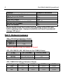
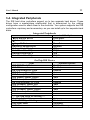
Specification:
Model
ENDAT-4946i/M
Form Factor
System Chipset
Mini-ITX 170 mm x 170 mm (6.69”x6.69”)
CPU Supporting
Memory
Ethernet
VGA
LCD Interface
DVI Interface
Display ratio
Serial / Parallel
Watchdog Timer
IDE Connector
SATA Connector
AUDIO
Expansion Slot
I/O Port
Digital IO
RS-422/485
USB Port
Power Supply
INTEL® 945GM + INTEL® ICH7
ENDAT-4946M: 533/667 FSB with 478 pin Intel® Celeron® M 423
processor
ENDAT-4946i: 533/667 FSB with 478 pin Intel® Core™ Solo, Intel®
Core™ Duo and Intel® Core™2 Duo processor
1 x 240 pin DDR2 socket supports DDR2 533/667 up to 2GB
Realtek 8111B PCIE Gigabit LAN
INTEL® GMA950 Graphic Controller with DVMT up to 224MB(max)
Onboard LVDS support 18/24/36/48bit Single/Dual Channels via internal
box header (optional)
Onboard DVI output via internal pin header (optional)
4:3 and 16:9
4 Serial Port w/+5V, +12V Power Selector / 1 Parallel port
Winbond 83627THG on-chip support 1 to 255 seconds/minutes
1 x 40pin IDE connector support UDMA 33/66/100
2 ports 300MHz Serial ATA Device
On-board AC’97 with 1.2W amplifier
One PCI slot with PCI 2.2 compliance
PS/2 Keyboard / Mouse Connector
2 x USB (2.0) + RJ-45 Connector w/LED indicator
D-sub Connector for COM 1, 2, 3 with POWER
1 x 25 Pins D-Sub Connector (LPT)
1 D-Sub Connector (VGA)
Internal pin header: KB, MS, USB (2.0) x4, AUX/CD-IN, SPDIF IN/OUT,
RF MIC IN, IR
8 bit input and 8 bit output (TTL level) by pin header
Via COM2 (Optional)
6 x USB2.0 onboard
ATX power supply
IV
The ENDAT-4946i/M System Board
TABLE OF CONTENTS
CHAPTER 1. INTRODUCTION....................................................... 1
1-1.
1-2.
1-3.
1-4.
FEATURES .............................................................................................. 2
UNPACKING ............................................................................................ 3
ELECTROSTATIC DISCHARGE PRECAUTIONS ................................... 3
MOTHERBOARD LAYOUT ...................................................................... 4
CHAPTER 2. SETTING UP THE MOTHERBOARD ....................... 5
2-1. JUMPERS AND CONNECTORS.............................................................. 5
2-2. INSTALLING MEMORY .......................................................................... 15
2-3. SHARED VGA MEMORY ....................................................................... 15
2-4. ASSIGNING IRQs FOR EXPANSION CARDS ....................................... 15
2-5. WATCHDOG TIMER…………………………………………………………. 16
2-6. DIGITAL I/O…………………………………………………………...………. 18
CHAPTER 3. AWARD BIOS SETUP ............................................ 20
3-1. STANDARD CMOS FEATURES............................................................. 21
3-2. ADVANCED BIOS FEATURES ............................................................... 22
3-3. ADVANCED CHIPSET FEATURES ........................................................ 24
3-4. INTEGRATED PERIPHERALS............................................................... 25
3-5. POWER MANAGEMENT SETUP........................................................... 39
3-6. PnP/PCI CONFIGURATIONS................................................................. 31
3-7. PC HEALTH STATUS ............................................................................. 32
User’s Manual
V
CHPATER 4. VGA, LCD, FEATURE............................................. 33
4-1. VGA FEATURE....................................................................................... 33
4-2. LVDS PANEL FEATURE......................................................................... 34
4-3. DRIVER UTILITY INSTALLATION GUIDE.............................................. 35
APPENDIX A: FLASH MEMORY UTILITY ................................... 36
APPENDIX B: CONNECTOR PIN ASSIGNMENT ....................... 37
APPENDIX C: LIMITED WARRANTY .......................................... 39
User’s Manual
1
Chapter 1. Introduction
ENDAT-4946i/M supports high performance processor of Intel® Celeron® M 423
(for ENDAT-4946M), Intel® Core™ Solo, Intel® Core™ Duo and Intel® Core™2
Duo processor (for ENDAT-4946i) with 533 and 667 Front Side Bus. It also
supports high speed DDR-2 memory with 64-bit wide interfaces with non-ECC
DIMM (up to 2GB). Only Double-Data-Rate Two Synchronous Dynamic Random
Access Memory is supported and the speed of memory can be 533 and 667 MHz.
ENDAT-4946i/M provides an integrated graphics (Intel® Graphics Media
Accelerator 950) accelerator delivering cost competitive 3D, 2D, and video
capabilities.
ENDAT-4946i/M video engines support video conferencing and other video
applications. Instead of a dedicated local graphics memory interface,
ENDAT-4946i/M uses a UMA configuration for optimal memory utilization and
performance that deliver 3D graphics with sharp images, fast rendering, smooth
motion and extreme detail.
ENDAT-4946i/M contains one integrated Serial ATA host controllers capable of
independent DMA operation on two ports. The SATA controllers are completely
software transparent with the IDE interface, while providing a lower pin count and
higher performance. The data transfer rate is up to 300 MB/s.
ENDAT-4946i/M is an ideal model for various kind of application:
- POS system
- KIOSK
- Interactive system
- Airport Terminal Controller
- Industrial controller
- Digital entertainment
- Embedded system equipment
2
The ENDAT-4946i/M System Board
1-1. Features
Basic Feature:
Board format: Mini-ITX (170mm x 170 mm)
Supports Socket 478 CPU (FSB 400/533/667 MHz)
Digital I/O: 8 bits in and 8 bits out (5V)
Supports DDR-2 533/667 SDRAM up to 2GB
Serial ATA connector x 2
Enhance IDE connector x 1
Multiple I/O ports: COM port x 4; USB (2.0) x 6
All COM ports with +5V, +12V power selector
Watchdog Timer
Realtek Gigabit LAN and Audio function onboard
Optional features:
On board chip provides LVDS interface (18/24/36/48 bit, single/dual
channels)
DVI Output interface
RS 422/485 via COM 2
Barebones system: niche into Unicorn U-6000 & U-8000 Chassis
Full Software Support:
Drivers for major operating systems and APIs: Windows 2000,
Windows XP, Direct3D, DirectDraw and DirectShow, OpenGL ICD
and DXVA for Windows 2000 and Windows XP
User’s Manual
3
1-2Unpacking
The motherboard comes securely packaged in a sturdy cardboard shipping carton.
In addition to the User’s Manual, the motherboard package includes the following
items:
ENDAT-4946i/M System Board
HDD / IO Cables
LCD cable (Optional)
CDROM Driver includes: Drivers for Windows 2000, XP and AMI / AWARD FLASH
ROM utilities.
Driver utilities for on-board VGA drivers, LAN adapter
If any of these items are missing or damage, please contact the dealer from whom
you purchase the motherboard. Save the shipping material and carton in the event
that you want to ship or store the board in the future.
Note: Please leave the motherboard in its original package until you are ready to
install it!
1-3. Electrostatic Discharge Precautions
Make sure you properly ground yourself before handling the motherboard, or other
system components. Electrostatic discharge can easily damage the components.
Note: You must take special precaution when handling the motherboard in dry or
air-conditioned environments.
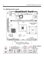
4
1-4. Motherboard Layout
The ENDAT-4946i/M System Board
5
User’s Manual
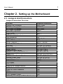
Chapter 2. Setting up the Motherboard
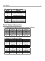
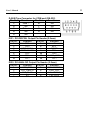
2-1. Jumpers And Connectors
Jumpers/Connectors Overview:
Function
Cooling Fan Connector
ATX Power Supply Connector
DVI Output Pin Header
LCD Panel Connector
LCD Voltage Selector
Clear CMOS
PS/2 Mouse/KB Pin Header
PS/2 Mouse/KB
USB Port
40-Pin IDE Connector
SATA 1, SATA2
Header for Case Panel
HDD LED
External Speaker
Buzzer On/Off
Hardware Reset Switch
ATX Power Supply On/Off Switch
Power LED
WDT Function Enable/Disable
External Power Good
Internal Power Good
DDR2 RAM Socket
CRT Output
IR Pin Header
COM1/2/3/4 Voltage Selector
COM1 Connector
COM2 & COM3 Connector
LPT1
LAN Connector
AC’97 Speaker Output
AC’97’ Speaker Output, MIC-In Pin Header
Jumpers/Connectors
FAN1, FAN2
ATXPWR
DVI1, DVI2
LVDS1
JP2
JBAT1
J1
CN1
CN8, J8, J9
IDE1
SATA 1, SATA2
JP6
JP6: Pin 1(-), Pin 2(+)
JP6: Pin 3(-), Pin 6(+)
JP6: Pin 4, Pin 5
JP6: Pin 7, Pin 8
JP6: Pin 9, Pin 10
JP6: Pin 11(-), Pin 12(+)
JP6: Pin 13, Pin 14
JP6: Pin 15, Pin 16
JP6: Pin 16, Pin 17
DIMM1
CN4
J3
JP5
CN2
CN5
CN3
CN8
CN9
J5
6
The ENDAT-4946i/M System Board
Function
5.1Ch Speaker output Pin Header
Line-In, CD-In Pin Header
COM2 Box Header
COM4 Box Header
RS232 / 422 / 485 Selector for COM2
DIGITAL I/O Pin Header
SPDIF Pin Header
Jumpers/Connectors
J6
J7
CN7
CN6
JP3, JP4
J2
J10
Please double-check the insertion and orientation of the LCD cable
before applying power. Improper installation will result in permanent
damage LCD panel.
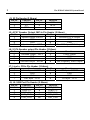
Part 1: Onboard Jumpers
JP2: LCD Voltage Selector (2.0mm)
LCD power
JP2 (2.54mm)
+3.3V
Pin-1, 2*
+5V
Pin-3, 4
+12V
Pin-5, 6
Caution: Improper setting will damage LCD panel.
JP3, JP4: RS232 / 422 / 485 Selector for COM2 (2.0mm)
TYPE
JP3 (3x4/2mm)
JP4 (2x3/2mm)
1-2, 4-5, 7-8, 10-11
1-2
RS-232 *
2-3, 5-6, 8-9, 11-12
3-4
RS-422
2-3, 5-6, 8-9, 11-12
5-6
RS-485
JP5: COM1/2/3/4 Voltage Selector (2.0mm)
Voltage
COM1
COM2
+12V
1-2
7-8
R.I*
3-4
9-10
+5V
5-6
11-12
COM3
13-14
15-16
17-18
COM4
19-20
21-22
23-24
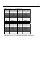
7
User’s Manual
JP6: Header for Case Panel (2.54mm)
Pin No.
Function
IDE LED
1(-), 2(+)
External Speaker
3(-), 6(+)
Buzzer On/Off
4,5
Hardware Reset Switch
7,8
ATX Power On/Off
9,10
Power LED
11(-), 12(+)
Close: Enable WDT function
13,14
External Power Good
15,16
Internal Power Good(Default)
16,17
Part 2: Onboard Connectors
J1: PS/2 Keyboard / Mouse Pin Header Connector (2.54mm)
Pin No.
Function
Pin No.
Function
KB Data
MS Data
1
2
KEY
KEY
3
4
GND
GND
5
6
+5V(DC)
+5V(DC)
7
8
KB_CLK
MS_CLK
9
10
J2: Digital I/O Pin Header (2.54mm)
Pin No.
Function
Pin No.
+5V
1
2
DIO-O0
3
4
DIO-O1
5
6
DIO-O2
7
8
DIO-O3
9
10
DIO-O4
11
12
DIO-O5
13
14
GND
15
16
DIO-O6
17
18
DIO-O7
19
20
+3.3V
21
22
Function
+5V
DIO-I0
DIO-I1
DIO-I2
DIO-I3
DIO-I4
DIO-I5
GND
DIO-I6
DIO-I7
+3.3V
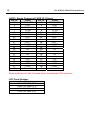
8
The ENDAT-4946i/M System Board
J3: IR Pin Header (2.54mm)
Pin No.
Function
Pin No.
VCC
1
4
N.C
2
5
IRRX
3
Function
GND
IRTX
J5: AC’97 Speaker Output, MIC-In Pin Header (2.54mm)
Pin No.
Function
Pin No.
Function
Speaker Output–RIGHT
Alternative LFE–Output
1
2
GND
GND
3
4
GND
GND
5
6
Speaker Output–LEFT
First MIC Input/CEN–Output
7
8
J6: 5.1Ch Speaker output Pin Header (2.54mm)
Pin No.
Function
Pin No.
Function
Surround Output – LEFT
Center Output
1
2
GND
GND
3
4
GND
GND
5
6
Surround Output – RIGHT
Low Frequency Effect Output
7
8
J7: Line-In, CD-In Pin Header (2.54mm)
Pin No.
Function
Pin No.
Line Input – RIGHT
1
2
GND
3
4
GND
5
6
Line Input – LEFT
7
8
J8, J9: USB Port Pin Header (2.54mm)
Pin No.
Function
Pin No.
Function
USB_VCC
USB_VCC
1
2
USBD 2/4USBD 3/53
4
USBD 2/4+
USBD 3/5+
5
6
USB_GND
USB_GND
7
8
USB_GND
USB_GND
9
10
Function
CD Input – RIGHT
GND
GND
CD Input – LEFT
9
User’s Manual
J10: SPDIF Pin Header (2.54mm)
Pin No.
Function
Pin No.
+5V
1
4
KEY
2
5
SPDIF-OUT
3
Function
GND
SPDIF-IN
ATXPWR: ATX Power Supply Connector (3.96mm)
Pin No.
Function
Pin No.
Function
+3.3V
+3.3V
1
2
+3.3V
-12V
3
4
GND
GND
5
6
+5V
PS-ON
7
8
GND
GND
9
10
+5V
GND
11
12
GND
GND
13
14
POWER OK
-5V
15
16
5V_SB
+5V
17
18
+12V
+5V
19
20
FAN1, FAN2: Cooling Fan Connector
Pin No.
Function
Sensor Pin.
1
+12V
2
GND
3
CN3: Printer (LPT1) Connector
Pin No.
Function
Pin No.
STB#
1
10
PD0
2
11
PD1
3
12
PD2
4
13
PD3
5
14
PD4
6
15
PD5
7
16
PD6
8
17
PD7
9
18-25
Function
ACK#
BUSY
PE
SLCT
AFD#
ERR#
INIT#
SLIN#
GND
10
CN4: CRT Connector
Pin No.
Function
RED
1
GREEN
2
BLUE
3
n/c
4
GND
5
GND
6
GND
7
GND
8
The ENDAT-4946i/M System Board
Pin No.
9
10
11
12
13
14
15
CN6: COM4 Pin Header (RS-232)
Pin No.
Function
Pin No.
DCD
1
6
RXD
2
7
TXD
3
8
DTR
4
9
GND
5
10
Function
n/c / +5V
GND
n/c
DDC DAT
H-Sync
V-Sync
DDC CLK
Function
DSR
RTS
CTS
RI
n/c
D-SUB Type Connector for COM2 port (RS-422 4 Wire)
Pin No.
Function
Pin No.
Function
–TXD
NA
1
6
+RXD
NA
2
7
+TXD
NA
3
8
NA
–RXD
4
9
NA
5
D-SUB Type Connector for COM2 port (RS-485 2 Wire)
Pin No.
Function
Pin No.
Function
Data –
NA
1
6
NA
NA
2
7
Data +
NA
3
8
NA
NA
4
9
NA
5
User’s Manual
D-SUB Type Connector for COM port (RS-232)
Pin No.
Function
Pin No.
Function
1
Data –
6
NA
2
NA
7
NA
3
Data +
8
NA
4
NA
9
NA
5
NA
DVI1: DVI-DIGITAL Output Pin Header (2.0mm)
Pin No.
Function
Pin No.
Function
TD2+5V
1
2
TD2+
KEY
3
4
EDID DATA
HPDET
5
6
EDID CLOCK
TD07
8
TD1TD0+
9
10
TD1
LVDS_GND
11
12
TLCTLC+
13
14
DVI2: DVI-ANALOG Output Pin Header (2.0mm)
Pin No.
Function
Pin No.
Function
CRT_RED
VGAVSYNC
1
2
CRT_GREEN
GND_CRT
3
4
CRT_BLUE
VGAHSYNC
5
6
n/c
CRT-Pin-6
7
8
11
12
The ENDAT-4946i/M System Board
IDE1: IDE Box Header (2x20 with 2.54mm)
Pin No.
Function
Pin No.
Function
1
IDE Reset#
2
GND
3
IDE data7
4
IDE data8
5
IDE data6
6
IDE data9
7
IDE data5
8
IDE data10
9
IDE data4
10
IDE data11
11
IDE data3
12
IDE data12
13
IDE data2
14
IDE data13
15
IDE data1
16
IDE data14
17
IDE data0
18
IDE data15
19
GND
20
N.C.
GND
21
IDE REQ
22
GND
23
IDE IOW#
24
GND
25
IDE IOR#
26
GND
27
IDE Ready
28
GND
29
IDE ACK#
30
31
IDE IRQ
32
N.C.
33
IDE A1
34
P66DET
35
IDE A0
36
IDE A2
37
IDECS1#
38
IDESC3#
39
HDLED#
40
GND
User’s Manual
LVDS1: Dual Channel of LVDS I/F (2.0mm)
Pin No.
Function
Pin No.
Function
VBL (+12V)
VBL (+12V)
1
2
GND
GND
3
4
DISP.ON/OFF
GND
5
6
LVDD
LVDD
7
8
GND
GND
9
10
RxO0+
RxO011
12
RxO1+
RxO113
14
RxO2+
RxO215
16
RxO3+
RxO317
18
RxOC+
RxOC19
20
GND
KEY
21
22
RxE0+
RxE023
24
RxE1+
RxE125
26
RxE2+
RxE227
28
RxE3+
RxE329
30
RxEC+
RxEC31
32
LVDD
LVDD
33
34
GND
GND
35
36
GND
GND
37
38
VBL (+12V)
VBL (+12V)
39
40
Please make sure the Pin 1 location before inserting the LCD connector.
13
14
The ENDAT-4946i/M System Board
LVDS1: Single Channel of LVDS I/F (2.0mm)
Pin No.
Signal
Pin No.
Signal
VBL (+12V)
VBL (+12V)
1
2
GND
GND
3
4
DISP.ON/OFF
GND
5
6
LVDD
LVDD
7
8
GND
GND
9
10
Rx0+
Rx011
12
Rx1+
Rx113
14
Rx2+
Rx215
16
Rx3+
Rx317
18
RxCLK+
TxCLK19
20
GND
KEY
21
22
n/c
n/c
23
24
n/c
n/c
25
26
n/c
n/c
27
28
n/c
n/c
29
30
n/c
n/c
31
32
LVDD
LVDD
33
34
GND
GND
35
36
GND
GND
37
38
VBL (+12V)
VBL (+12V)
39
40
Please make sure the Pin 1 location before inserting the LCD connector.
LCD Panel Number:
Panel Number
1024x768 24Bit 1CH
1280x1024 48Bit 2CH
1280x768 24Bit 1CH
1366x768 24Bit 1CH
User’s Manual
15
2-2. Installing Memory
ENDAT-4946i/M system board offers one 240pin DDR-2 SDRAM socket supports
up to 2GB memory and the speed can be 533 / 667 MHz.
2-3. Shared VGA Memory
ENDAT-4946i/M is using built-in INTEL® GMA950 Graphic with INTEL DVMT 3.0
up to 224MB of system memory. The amount of video memory on motherboard
determines the number of colors and the video graphic resolution.
2-4.
Assigning IRQs for Expansion Cards
Some expansion cards require an IRQ (Interrupt request vector) to operate.
Generally, each IRQ must be exclusively assigned to specific use. In a standard
design, there are 16 IRQ available with 11 of them already in used by other part of
the system.
Some PCI expansion cards need IRQ; any remaining IRQ could be assigned to
PCI Bus. Microsoft’s Diagnostic (MSD.EXE) utility included in the Windows
directory can be used to see their map. Clients can not have more than one device
apply the same IRQ in the system or it will cause the system hang up, crash, and
unexpected results. To simplify the process, this motherboard complies with the
Plug and Play (PnP) specifications, which was developed to allow automatic
system configuration. Whenever a PnP-compliant card is added to the system,
PnP card and IRQs will automatically assigned if available. The PCI and PnP
configuration in the BIOS setup utility can indicate which IRQs have being used by
Legacy cards.
In the PCI Bus design, the BIOS is automatically assigned an IRQ to a PCI slot that
has a card in it which requires an IRQ. To install PCI cards via riser card, you need
to set the correct “ADSEL” and “INT” (interrupt) assignment on the jumper of riser
card.
16
The ENDAT-4946i/M System Board
IRQ
0
1
2
3
4
5
6
7
8
9
10
11
12
13
14
15
2-5.
Status
Used
Used
Used
Used
Used
Used
Used
Used
Used
Used
Used
Used
Used
Used
Used
Used
Assignment
Timer
Keyboard
Second 8259
COM2
COM1
COM3
Floppy Disk
LPT1
RTC
Audio
COM4
LAN Adapter (on board)
PS/2 Mouse
Coprocessor
Hard Disk (IDE 1)
Reserved (IDE 2)
Watchdog Timer
Watchdog Timer (WDT) is a special design for system monitoring to secure the
system work normally. WDT has an independent clock from the oscillator and
could set time and clear/refresh WDT counter function. When time is up, WDT will
send hardware RESET signal to reset system.
Timeout Value Range
-1 to 255
-Second or Minute
User’s Manual
17
Program Sample
#include <stdio.h>
#include <dos.h>
#include <dir.h>
void show_ver();
void main()
{
unsigned int tt;
clrscr();
show_ver();
tt=0;
while((tt==0)||(tt>255))
{
printf(“\n\nPlease key in how many seconds you want to reset system
(1~255):”);
scanf(“%d”,&tt);
}
outportb(0x2e,0x87); //Unlock register
outportb(0x2e,0x87); //Unlock register
outportb(0x2e,0x07); //Set Logic Device number pointer
outportb(0x2f,0x08); //Set Logic Device number
outportb(0x2e,0xf5); //Set active register is CRF5
outportb(0x2f,0x00); //Set register value (bit3=1: minute. =0: second)
outportb(0x2e,0xf7); //Set active register is CRF7
outportb(0x2f,0x00); //Disable all WDT interrupt (bit7=Mouse,
bit6=Keyboard)
outportb(0x2e,0xf6); //Set active register is CRF6
outportb(0x2f,tt); //Set time out value of WDT
}
void show_ver()
{
unsigned char tmp0;
printf(“Designed by ROBERT LIOU of UNICORN computer corp.
\n2004/03/02 release version:1.0a\n”);
printf(“This program is design for test Watchdog Timer for W83627.\n”);
}
18
The ENDAT-4946i/M System Board
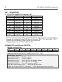
2-6.
Digital I/O
1) Pin out of digital I/O header (J2):
Pin No.
1
3
5
7
9
11
13
15
17
19
21
Function
+5V
DIO-O0
DIO-O1
DIO-O2
DIO-O3
DIO-O4
DIO-O5
GND
DIO-O6
DIO-O7
+3.3V
Pin No.
2
4
6
8
10
12
14
16
18
20
22
Function
+5V
DIO-I0
DIO-I1
DIO-I2
DIO-I3
DIO-I4
DIO-I5
GND
DIO-I6
DIO-I7
+3.3V
This function is supported by onboard super I/O chip; it can be control easily by
change the register of super I/O chip via I/O port “2Eh” “2Fh” and “4Eh” “4Fh”.
Please see the sample code of below for implement.
Voltage tolerance: +/- 5% with 0V to +5V.
2) Digital I/O control port (2E,2Fh):
Register configuration:
Bit No
7
6
Map
IN3
IN2
5
OUT3
4
OUT2
3
OUT1
2
OUT0
1
IN1
Sample code for input bit 0~3 (using Turbo C/C++ 3.0):
#define input_port 0x2f
outportb(0x2e,0x87); //Unlock register
outportb(0x2e,0x87); //Unlock register
outportb(0x2e,0x07); //Set Logic Device number pointer
outportb(0x2f,0x07); //Set Logic Device number
outportb(0x2e,0xF1); //Set active register is CRF1
read_data=inportb(input_port); // Read digital input data
printf(“DIO-Input=%02X\n”,read_data); //Show digital input data on screen
0
IN0
19
User’s Manual
Sample code for output bit 0~3 (using Turbo C/C++ 3.0):
outportb(0x2e,0x87); //Unlock register
outportb(0x2e,0x87); //Unlock register
outportb(0x2e,0x07); //Set Logic Device number pointer
outportb(0x2f,0x07); //Set Logic Device number
outportb(0x2e,0xF2); //Set active register is CRF2
outportb(0x2f,0x00); //Write data to digital output
3) Digital I/O control port (4E,4Fh):
Register configuration:
Bit No
7
6
Map
IN7
IN6
5
OUT7
4
OUT6
3
OUT5
2
OUT4
1
IN5
Sample code for input bit 4~7(using Turbo C/C++ 3.0):
#define input_port 0x2f
outportb(0x4e,0x87); //Unlock register
outportb(0x4e,0x87); //Unlock register
outportb(0x4e,0x07); //Set Logic Device number pointer
outportb(0x4f,0x07); //Set Logic Device number
outportb(0x4e,0xF1); //Set active register is CRF1
read_data=inportb(input_port); // Read digital input data
printf(“DIO-Input=%02X\n”,read_data); //Show digital input data on screen
Sample code for output bit 4~7(using Turbo C/C++ 3.0):
outportb(0x4e,0x87); //Unlock register
outportb(0x4e,0x87); //Unlock register
outportb(0x4e,0x07); //Set Logic Device number pointer
outportb(0x4f,0x07); //Set Logic Device number
outportb(0x4e,0xF2); //Set active register is CRF2
outportb(0x4f,0x00); //Write data to digital output
0
IN4
20
The ENDAT-4946i/M System Board
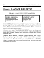
Chapter 3. AWARD BIOS SETUP
Phoenix – Award BIOS CMOS Setup Utility
> Standard CMOS Features
> Advanced BIOS Features
> Advanced Chipset Features
> Integrated Peripherals
> Power Management Setup
> PnP/PCI Configurations
> PC Health Status
> Load Optimized Defaults
> Set Supervisor Password
> Set User Password
> Save & Exit Setup
> Exit Without Saving
Use the CMOS setup program to modify the system parameters to reflect the
environment installed in your system and to customize the system as desired.
Press the <DEL> key to enter into the CMOS setup program when you turn on the
power. Settings can be accessed via arrow keys. Press <Enter> to choose an
option to configure the system properly.
In the main menu, press F10 or “SAVE & EXIT SETUP” to save your changes and
reboot the system. Choose “EXIT WITHOUT SAVING” to ignore the changes and
exit the setup procedure. Pressing <ESC> at anywhere during the setup will return
to the main menu.
“Advanced BIOS Features”, “Advanced Chipset Features” and “PnP/PCI
Configurations” requires board knowledge on PC/AT system architecture and Intel
chipset specification. They intend to be used by well-trained technicians and
experienced users. Press the <F10> key to save CMOS setting to EEPROM,
Press <F7> key can load CMOS setting from EEPROM. Incorrect setup could
cause system malfunctions.
21
User’s Manual
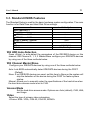
3-1. Standard CMOS Features
The Standard Setup is used for the basic hardware system configuration. The main
function is for Data/Time and Hard Disk Drive settings.
Item
Date (mm:dd:yy)
Time (hh:mm:ss)
>IDE Channel 0 Master:
>IDE Channel 0 Slave :
>IDE Channel 1 Master:
>IDE Channel 1 Slave :
Video
Halt On
Available Options:
Auto
Auto
Auto
Auto
EGA/VGA
All , But Keyboar
˙IDE HDD Auto-Detection
Press <Enter> to auto-detect the parameters of the IDE/SATA device on this
channel. IDE Channel 0, 1, 2, 3 Master/Slave configure your IDE/SATA devices
by using one of the three methods below:
˙IDE Channel Master/Slave
Configure your IDE/SATA devices by using one of the three methods below:
Auto: Lets BIOS automatically detect IDE/SATA devices during the POST.
(Default)
None: If no IDE/SATA devices are used, set this item to None so the system will
skip the detection of the device during the POST for faster system
startup.
Manual: Allows you to manually enter the specifications of the hard drive when
the hard drive access mode is set to CHS.
˙Access Mode
Set the hard drive access mode. Options are: Auto (default), CHS, LBA,
and Large.
˙Video
Select the type of primary video subsystem.
<Choice: EGA / VGA, CGA 40, CGA 80, MONO>
22
The ENDAT-4946i/M System Board
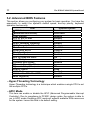
3-2. Advanced BIOS Features
This section allows you configuring your system for basic operation. You have the
opportunity to select the system’s default speed, boot-up priority, keyboard
operation and security.
Item
Available Options:
Press Enter
>CPU Feature
Press Enter
>Hard Disk Boot Priority
Virus Warning
Disabled
CPU L1 & L2 Cache
Enabled
CPU L3 Cache
Enabled
Hyper-Threading Technology
Enabled
Quick Power On Self Test
Enabled
First Boot Device
Hard Disk
Second Boot Device
CDROM
Third Boot Device
LS120
Boot Other Device
Enabled
Boot Up NumLock Status
On
Gate A20 Option
Normal
Typematic Rate Setting
Disabled
Typematic Rate (Chars/Sec)
6
Typematic Delay (Msec)
250
Security Option
Setup
APIC Mode
Enabled
OS Select For DRAM > 64MB
Non-OS2
Small Logo(EPA)
Enabled
․Hyper-Threading Technology
Hyper-Threading technology is a technique which enables a single CPU to act
like multiple CPU’s.
․APIC Mode
This item can enable or disable the APIC (Advanced Programmable Interrupt
Controller). Due to compliance to PC2001 design guide, the system is able to
run in APIC mode. Enabling APIC mode will expand available IRQs resources
for the system. Leave this field in its default setting.
23
User’s Manual
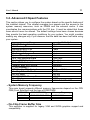
3-3. Advanced Chipset Features
This section allows you to configure the system based on the specific features of
the installed chipset. This chipset manages bus speeds and the access to the
system memory resources, such as DRAM and the external cache. It also
coordinates the communications with the PCI bus. It must be stated that these
items should never be altered. The default settings have been chosen because
they provide the best operating conditions for your system. You might consider
making any changes only if you discover that the data has been lost while using
your system.
Item
DRAM Timing Selectable
CAS Latency Time
DRAM RAS# to CAS
DRAM RAS# Precharge
Precharge dealy
System Memory Frequency
SLP_S4# Assertion Width
System BIOS Cacheable
Video BIOS Cacheable
Memory Hole At 15M-16M
** VGA Setting **
PEG/Onchip VGA Control
On-Chip Frame Buffer Size
DVMT Mode
DVMT/FIXED Memory Size
Boot Display
Panel Number
Available Options:
By SPD
Auto
Auto
Auto
Auto
Auto
4 to 5 Sec.
Enabled
Enabled
Disabled
Onboard VGA
8MB
DVMT
128MB
CRT
1024x768 24Bit 1CH
․System Memory Frequency
This main board supports different memory frequencies depend on the CPU
FSB (Front Side Bus) and the type of DDR DIMM.
CPU FSB
DDR2 DIMM Type
Memory Frequency
667 MHz
PC2-5300/PC2-4200
667/533 MHz
533 MHz
PC2-4200
533 MHz
․On-Chip Frame Buffer Size
This selection is supplied for legacy VGA and SVGA graphics support and
compatibility.
24
The ENDAT-4946i/M System Board
․DVMT Mode
This field is used to select the type of DVMT mode. DVMT (Dynamic Video
Memory Technology) is an architecture that offers breakthrough performance
for the motherboard through efficient memory utilization.
A fixed-size fragment of the system memory is allocated to the
FIXED
graphics core.
The graphics driver allocates memory as needed for running
DVMT
graphics applications and is cooperatively using this memory with
other system components.
This mode guarantees that at least 64MB of memory is available to
BOTH
the graphics core, with a possibility to increase this amount to
128MB, if necessary.
․Boot Display
This field is used to select the type of display to use when the system boots.
EFP means DVI or LCD display by main board.
CRT
Select this option if you want the system to boot the CRT display.
Select this option if you want the system to boot the DVI or LCD
EFP
flat panel display. (Optional Item)
Select this option if you want the system to boot both of the CRT
CRT+EFP
and DVI or LCD display. (Optional Item)
․Panel Number (Optional Item)
If you apply one of the standard panels shown above, select the appropriate
option according to the type of panel that you apply. Or, please contact your
dealer or sales representative for custom-made BIOS that will suit the panel that
you apply. When main board offers DVI output, this option will not be shown.
Panel Number
1024x768 24Bit 1CH
1280x1024 48Bit 2CH
1280x768 24Bit 1CH
1366x768 24Bit 1CH
25
User’s Manual
3-4. Integrated Peripherals
The IDE hard drive controllers support up to two separate hard drives. These
drives have a master/slave relationship that is determined by the cabling
configuration used to attach them to the controller. Your system supports two IDE
controllers--a primary and a secondary--so you can install up to four separate hard
disks.
Integrated Peripherals
Item
>OnChip IDE Device
>Onboard Device
>SuperIO Device
Onboard Lan Boot ROM
Onboard Serial Port 3
Serial Port 3 Use IRQ
Onboard Serial Port 4
Serial Port 4 Use IRQ
Available Options:
Press Enter
Press Enter
Press Enter
Disabled
3E8
IRQ5
2E8
IRQ10
OnChip IDE Device
Item
IDE HDD Block Mode
IDE DMA transfer access
On-Chip Primary PCI IDE
IDE Primary Master PIO
IDE Primary Slave PIO
IDE Primary Master UDMA
IDE Primary Slave UDMA
On-Chip Secondary PCI IDE
IDE Secondary Master PIO
IDE Secondary Slave PIO
IDE Secondary Master UDMA
IDE Secondary Slave UDMA
Available Options:
Enabled
Enabled
Enabled
Auto
Auto
Auto
Auto
Enabled
Auto
Auto
Auto
Auto
*** On-Chip Serial ATA Setting ***
On-Chip Serial ATA
SATA PORT Speed Settings
PATA IDE Mode
SATA Port
Auto
Disabled
Secondary
P0,P2 is Primary
26
The ENDAT-4946i/M System Board
Onboard Device
Item
Available Options:
Enabled
Enabled
Enabled
Enabled
USB Controller
USB 2.0 Controller
USB Keyboard Support
AC97 Audio Select
SuperIO Device
Item
POWER ON Function
KB Power ON Password
Hot Key Power ON
Onboard Serial Port 1
Onboard Serial Port 2
UART Mode Select
RxD, TxD Active
IR Transmission Delay
UR2 Duplex Mode
Use IR Pins
Onboard Parallel Port
Parallel Port Mode
EPP Mode Select
ECP Mode Use DMA
PWRON After PWR-Fail
Available Options:
Button ONLY
Enter
Ctrl-F1
3F8/IRQ4
2F8/IRQ3
Normal
Hi,Lo
Enabled
Half
IR-Rx2Tx2
378/IRQ7
ECP+EPP
EPP1.7
3
Off
․Onboard LAN Boot ROM
The default setting is enabled or disabled LAN boot up function.
․IDE HDD Block Mode
Block mode is also called block transfer, multiple commands, or multiple sectors
read/write.
․IDE Primary Master/Slave PIO and IDE Secondary
Master/Slave PIO
The four IDE PIO (programmed Input/Output) fields let you set a PIO mode (0-4)
for each IDE device that the internal PCI IDE interface supports. Modes 0
through 4 provide successively increased performance. In Auto mode, the
27
User’s Manual
system automatically determines the best mode for each device.
․IDE Primary Master/Slave UDMA and IDE Secondary
Master/Slave UDMA
These fields allow you to set the Ultra DMA in use. When Auto is selected, the
BIOS will select the best available option after checking your hard drive or
CD-ROM.
․On-Chip Serial ATA
Disabled
Auto
Combined Mode
Enhanced Mode
SATA Only
Disables the onboard SATA.
The system will detect the existing SATA and IDE drives
then automatically set them to the available master/slave
mode.
This option allows you to use both IDE and SATA drives;
allowing a maximum of 4 drives. You must manually set
the SATA drives’ master/slave mode in the “Serial ATA
Port0 Mode” and “Serial ATA Port1 Mode” fields.
This option allows you to use both IDE and SATA drives;
allowing a maximum of 6 drives.
This option automatically sets the SATA drives to Primary
Master and Secondary Master modes. Since both drives are
in master mode, you cannot set the IDE drives to Master
mode. The “Serial ATA Port0 Mode” and “Serial ATA
Port1 Mode” fields will not be configurable.
․SATA PORT Speed Settings
The SATA PORT Speed Settings option controls the maximum access speed
allowed for the connected SATA devices, with the GEN I setting used for
SATA-150 type devices and GEN II used for SATA II type devices.
․PATA IDE Mode
These fields are used to select the master/slave mode of the serial ATA drives.
Make sure they do not conflict with the settings of the IDE hard drives.
․USB Controller
Select “Enabled” if your system contains a Universal Serial Bus (USB) controller
and you have a USB peripheral.
28
The ENDAT-4946i/M System Board
․USB 2.0 Controller
The options for this field are Enabled and Disabled. By default, this field is set to
Disabled. In order to use USB 2.0, necessary OS drivers must be installed first.
․AC97 Audio Select
The AC97 Audio Select option allows the user to enable or disable onboard
audio function.
․UART Mode Select
Select an operating mode for the serial port 2.
<Choice: IrDA, ASKIR, Normal>
․Parallel Port Mode
This field allows you to determine parallel port mode function.
<Choice: SPP, EPP, ECP, ECP + EPP, Normal>
․PWRON After PWR-Fail
This item allows you to select if you want to power on the system after power
failure
29
User’s Manual
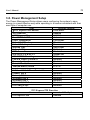
3-5. Power Management Setup
The Power Management Setup allows users configuring the system to save
energy in a most effective way while operating in a manner consistent with their
own style of computer use.
Item
Available Options:
Press Enter
>PCI Express PM Function
ACPI function
Enabled
ACPI Support Type
S1(POS)
Run VBIOS if S3 Resume
Auto
Power Management
User Define
Video Off Method
Blank Screen
Video Off In Suspend
Yes
Suspend Type
Stop Grant
Suspend Mode
Disabled
HDD Power Down
Disabled
Soft-Off by PWR-BTTN
Instant-Off
CPU THRM-Throttling
75.0%
USB KB Wake-Up From S3
Disabled
Resume by Alarm
Disabled
Date(of Month) Alarm
0
Time(hh:mm:ss) Alarm
0:0:0
** Reload Global Timer Events **
Primary IDE 0
Primary IDE 1
Secondary IDE 0
Secondary IDE 1
FDD,COM,LPT Port
PCI PIRQ[A-D]#
Disabled
Disabled
Disabled
Disabled
Disabled
Disabled
PCI Express PM Function
Item
PCI Express PME
Available Options:
Enabled
30
The ENDAT-4946i/M System Board
․ACPI Function
This function should be enabled only in operating systems that support ACPI.
Currently, only Windows® 98SE/2000/ME/XP supports this function. When this
field is enabled, the system will ignore the settings in the “Suspend Mode” and
“HDD Power Down” fields. If you want to use the Suspend to RAM function,
make sure this field is enabled then select“S3 (STR)” in the field below.
․ACPI Suspend Type
This field is used to select the type of Suspend mode.
Enables the Power On Suspend function.
S1(POS)
Enables the Suspend to RAM function.
S3(STR)
If S3 state is supported by the system, by default [S3] is
S1 & S3
automatically selected. Otherwise [S1] is selected.
․Power Management
This field allows you to select the type of power saving management modes.
․Video Off Method
This field defines the Video Off features.
Writes blanks to the video buffer.
Blank Screen
V/H SYNC + Blank Enables the Suspend to RAM function.
Allows BIOS to control the video display.
DPMS
․Soft-Off by PWR-BTTN
This field defines the power-off mode when using an ATX power supply.
․CPU THRM-Throttling
When the system enters Doze mode, the CPU clock runs only part of the time.
You may select the percent of time that the clock runs.
.
31
User’s Manual
3-6. PnP/PCI Configurations
This section describes the configuration of the PCI bus system. PCI is a system
that allows I/O device to operate at speeds nearing the speed of the CPU itself,
when communicating with its own special components. This section covers some
very technical items. It is strongly recommended that only experienced users make
any changes to the default settings.
Item
Init Display First
Reset Configuration Data
Resources Controlled By
IRQ Resources
Available Options:
PCI Slot
Disabled
Auto(ESCD)
Press Enter
․Reset Configuration Data
Enabled
Disabled
The BIOS will reset the Extended System Configuration Data
(ESCD) once automatically. It will then recreate a new set of
configuration data.
The BIOS will not reset the configuration data.
․Resources Controlled By
Auto(ESCD)
Manual
The system will automatically detect the settings for you.
Choose the specific IRQ in the “IRQ Resources” field.
․PCI/VGA Palette Snoop
When set to [Enabled], multiple VGA devices operating on different buses can
handle data from the CPU on each set of palette registers on every video device.
Bit 5 of the command register in the PCI device configuration space is the VGA
Palette Snoop bit (0 is disabled).
32
The ENDAT-4946i/M System Board
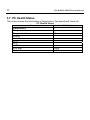
3-7. PC Health Status
This screen shows the information of temperature, Fan speed and Vcore etc.
PC Health Status
Item
Temperature 1
Temperature 2
Temperature 3
VcoreA
VcoreB
+3.3 V
+5 V
+ 12 V
CPU Fan
System Fan
Available Options:
℃
℃
℃
RPM
RPM
User’s Manual
33
Chapter 4. VGA, LCD Feature
4-1.
VGA Feature
ENDAT-4946i/M provides an integrated graphics (Intel® Graphics Media
Accelerator 950) accelerator delivering cost competitive 3D, 2D, and video
capabilities. It contains an extensive set of instructions for 3D operations, BLT
(Block Level Transfers) and Stretch BLT operations, motion compensation,
overlay, and display control. ENDAT-4946i/M video engines support video
conferencing and other video applications. Instead of a dedicated local graphics
memory interface, ENDAT-4946i/M applies UMA configuration for optimal memory
utilization and performance that deliver 3D graphics with sharp images, fast
rendering, smooth motion and extreme detail.
The Intel® 945GM Express chipset's low power design enables up to 28% less
average power consumption compared to previous generations. Featuring the
Intel® Graphics Media Accelerator 950, the Intel 945GM Express chipset delivers
up to 2 x improvements in graphics performance over the previous generation
chipset. The Intel® 945GM Express chipset enables up to 25% higher data
transfer rate compared to the previous generation bus speed.
ENDAT-4946i/M applies Intel® DVMT 3.0 for optimum the system utilization via
system chipset. DVMT is a concept be applied in the Intel® 945GM chipset
wherein the optimum amount of memory is dynamically allocated and de-allocated
as needed for balanced graphics and system performance, through Intel® Direct
AGP and a highly efficient memory utilization scheme.
The on-board INTEL® GMA950 Graphic Controller supports a full AGP
implementation internally to remain compatible with existing software and
programming models. However, since the engine is integrated, it enjoys a higher
bandwidth and lower latency than is possible with discrete solutions.
The controller of ENDAT-4946i/M supports 3 types of display: CRT, DVI and LVDS
panel.
34
4-2.
The ENDAT-4946i/M System Board
LVDS Panel Feature (optional)
The on-board graphic controller supports industry standard LCD panel, LVDS
interface only, with 1 channel (18 or 24) and 2 channels (36 or 48bit) data width.
LVDS interface provides low voltage, high speed and low EMI serial DC-balanced
differential data via optional onboard LVDS.
The flat panel interface provides or supports following functions for various panels:
- Generates LVDS flat panel channels like clock and data channel.
- Generates different video data formats to directly drive different types of
panels (18, 24, 36 or 48bit)
- Wide screen resolution as 16:9 or 16:10.
- Vertical and horizontal expansion of video displays to LCD panel resolution
- Vertical and horizontal centering
- Panel power sequence
Please note that the default setting is with “CRT”. If the LCD display features is
required, the setting will need to be revised in the system BIOS setting: “CRT+EFP”
under “Advanced Chipset Features” unless clients specified the display type while order.
User’s Manual
4-3.
35
Driver Utility Installation Guide
When finishing the installation of Windows platform (2000/XP), please install the
relative “INF” driver of Intel® chipsets firstly for compliance compatibility of
hardware environment.
Please follow the step of CD-ROM driver and complete the VGA, AUDIO,
ETHERNET and USB2.0 setup procedure. Insert the support CD that supplied with
motherboard into CD-ROM driver, which enable the access with auto-run mode; or
double –click the CD driver icon in “My Computer” to bring up the screen.
Please download or check from Intel® Web site: www.intel.com if you prefer to install the drivers
individually or you need more information.
36
The ENDAT-4946i/M System Board
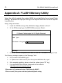
Appendix A: FLASH Memory Utility
Using this utility to update the system BIOS from a disk file to the on board Flash
memory. Be aware the improper change of the system BIOS will cause the system
to malfunction.
Using utility as follows:
1.
Insert the FLASH memory utility distribution floppy diskette in drive A:
2.
At the DOS prompt, type A:>AWDFLASH and press <Enter>
AwardBIOS FLASH Utility V8.63E
C>Phoenix Technologies Ltd. All Rights Reserved
Flash Type –
File Name to Program:
Message:
3.
Enter the name of the system BIOS disk file into the "File Name to Program" field
The following message appears in the "Message" field
4.
Do you want to save BIOS (y/n)?
5.
To update the FLASH memory from the system BIOS disk file, type Y
6.
After complete updating, please re-boot the system (press “F1” key)
7.
For upgrade BIOS procedure, please refer to our web site:
http://www.unicorn-computer.com.tw
* Please turn off system and clear CMOS data by JBAT1.
* Please restart your system and load optimal defaults setting.
37
User’s Manual
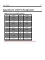
Appendix B: LCD Pin Assignment
LVDS1: Dual Channel LVDS (2.54mm)
Pin No.
1
3
5
7
9
11
13
15
17
19
21
23
25
27
29
31
33
35
37
39
Signal
VBL (+12V)
GND
DISP.ON/OFF
LVDD
GND
RxO0+
RxO1+
RxO2+
RxO3+
RxOC+
GND
RxE0+
RxE1+
RxE2+
RxE3+
RxEC+
LVDD
GND
GND
VBL (+12V)
Pin No.
2
4
6
8
10
12
14
16
18
20
22
24
26
28
30
32
34
36
38
40
Signal
VBL (+12V)
GND
GND
LVDD
GND
RxO0RxO1RxO2RxO3RxOCKEY
RxE0RxE1RxE2RxE3RxECLVDD
GND
GND
VBL (+12V)
Please make sure the Pin 1 location before inserting the LCD connector.
38
The ENDAT-4946i/M System Board
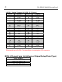
LVDS1: Single Channel of LVDS I/F (2.0mm)
Pin No.
Signal
Pin No.
Signal
VBL (+12V)
VBL (+12V)
1
2
GND
GND
3
4
DISP.ON/OFF
GND
5
6
LVDD
LVDD
7
8
GND
GND
9
10
Rx0+
Rx011
12
Rx1+
Rx113
14
Rx2+
Rx215
16
Rx3+
Rx317
18
RxCLK+
TxCLK19
20
GND
KEY
21
22
n/c
n/c
23
24
n/c
n/c
25
26
n/c
n/c
27
28
n/c
n/c
29
30
n/c
n/c
`31
32
LVDD
LVDD
33
34
GND
GND
35
36
GND
GND
37
38
VBL (+12V)
VBL (+12V)
39
40
Please make sure the Pin 1 location before inserting the LCD connector.
BIOS LCD panel type list (Advance Chipset Setup/Panel Type)
Panel Number
1024x768 24Bit 1CH
1280x1024 48Bit 2CH
1280x768 24Bit 1CH
1366x768 24Bit 1CH
User’s Manual
39
Appendix C: Limited Warranty
Standard two years limited warranty on all our ENDAT series all-in-one
motherboards and embedded boards. Products that become defective during the
warranty period shall be repaired, or subject to manufacturer’s option, replaced.
The limited warranty applies to normal proper usage of the hardware and does not
cover products that have been modified or subjected to unusual electrical or
physical stress. Unicorn Computer Corp is not liable to repair or replace defective
goods caused by improper using or use of unauthorized parts. The following
situations will be charged:
1. The products during the warranty but defective caused by improper using or
artificial external pressure and result in the components damages. According to
the damage situation, the manufacturer has the rights to decide to repair or not.
The manufacturer will charge the parts/repair cost and the returning shipping
charge.
2. The products out of warranty will charge the parts/repair cost and the returning
shipping charge as per the repair status.
3. The manufacturer has the rights to decide to repair or not based on the stock of
parts for the products which are phased out of the production.
4. Please e-mail or fax the RMA Service Request Form when have the defective
products.
40
The ENDAT-4946i/M System Board
RMA SERVICE REQUEST FORM
When requesting RMA service, please fill out this “RMA Service Request Form”.
This form needs to be shipped with your returns. Service cannot begin until we
have this information.
RMA NO.:
Company:
Person to Contact:
Phone No:
Purchase Date :
Fax No. :
Applied Date :
Return Shipping Address:
Model No.
Serial No.
Problem Code
Remark
User’s Manual
Issue Code of defect.
01 Second Times R.M.A.
11 Memory Socket Bad
02 No Screen (No Boot)
12 Hang Up Hardware
03 VGA (Display) Fail
13 Hang Up Software
04 CMOS Data Lost
14 PCB Problem
05 FDC Fail
15 CPU Socket Bad
06 HDC Fail
16 LAN Fail
07 Bad Slot
17 Audio Fail
08 BIOS Problem
18 Serial Port Fail
09 Keyboard Controller Fail
19 Parallel Port Fail
10 Cache RAM Problem
20 Others
Please specify the following when returning the RMA boards:
(1) Hardware Configuration (2) OS or Software (3) Testing Program
___________________
Authorized Signature
41