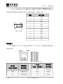
1
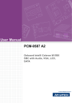
EC51712CLDNA(B) Embedded Single Board Computer with CPU/LVDS/VGA/SSD/LAN/AUDIO Version: C00
Announcement What contained in this User Manual does not represent the commitments of EVOC Company. EVOC Company reserves the right to revise this User Manual, without prior notice, and will not be held liable for any direct, indirect, intended or unintended losses and/or hidden dangers due to installation or improper operation. Before purchasing, please have a detailed understanding of the product performance to see whether it meets your requirements. EVOC is a registered trademark of EVOC Intelligent Technology Co., Ltd. All trademarks, registered trademarks, and trade names used in this User Guide are the property of their respective owners. EVOC Intelligent Technology Co., Ltd. ©2009, Copyright Reserved. No part of this manual can be reproduced in any form or by any means, such as in electronic or mechanical way, without permission in writing from EVOC. Safety Instructions 1. Please carefully read the users’ manual before handling the product; 2. For the board which is not ready to be installed, please put it in the antistatic packaging; 3. Before taking the board out from antistatic packaging, please put your hand on grounded metal object for a while (about 10 seconds) to discharge static; 4. Please wear static protective gloves when holding the board; and always hold the board by edges; 5. Before inserting, removing or reconfiguring the motherboard or the expansion card, please firstly disconnect the AC power or unplug the AC power cable from the power source to prevent damage to the product and ensure your personal safety; 6. Before removing the boards or PC boxes, firstly turn off all power resources and unplug the power cable from power source; 7. For PC Box products, when inserting or removing boards, please disconnect the AC power in advance; 8. Before connecting or disconnecting any device, make sure all power cables are unplugged in advance; 9. To avoid unnecessary damage caused by turning on/off computer frequently, wait at least 30 seconds before returning on the computer.
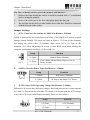
Contents Chapter 1 Product Introduction ................................................................................1 Overview ............................................................................................................1 Mechanical Dimension, Weight and Environment.................................................1 Typical Power Consumption ................................................................................2 Microprocessor ...................................................................................................2 Chipset ...............................................................................................................2 System Memory ..................................................................................................2 Video Function....................................................................................................2 Network Function................................................................................................2 Audio Function ...................................................................................................2 Expansion Bus ....................................................................................................3 CF Card ..............................................................................................................3 Power Feature .....................................................................................................3 Watchdog Function..............................................................................................3 I/O Interfaces ......................................................................................................3 Chapter 2 Installation...............................................................................................4 Product Outline ...................................................................................................4 Locations of Interfaces ........................................................................................5 Motherboard Structure.........................................................................................6 Jumper Settings...................................................................................................7 Install System Memory........................................................................................8 Video Interface....................................................................................................9 LCD Backlight Control Interface .......................................................................11 SATA Interface..................................................................................................11
Hotswap of SATA Hard Disk............................................................................ 11 IDE Interface .................................................................................................... 13 USB Interface................................................................................................... 15 Keyboard/Mouse Interface ................................................................................ 15 Parallel Port...................................................................................................... 16 Serial Port......................................................................................................... 16 Network Interface ............................................................................................. 18 Audio Interface................................................................................................. 19 Digital I/O Interface.......................................................................................... 19 Power Interface................................................................................................. 19 Fan Interface..................................................................................................... 21 Status Indicating Control Interface..................................................................... 21 CF Card............................................................................................................ 22 PCI Interface .................................................................................................... 23 Install CPU....................................................................................................... 25 Install CPU Fan ................................................................................................ 25 Chapter 3 BIOS Setup ........................................................................................... 26 BIOS Overview ................................................................................................ 26 BIOS Parameter Setup ...................................................................................... 26 BIOS Basic Function Setup............................................................................... 27 The System Resources Managed by BIOS under x86 Platform ........................... 39 Chapter 4 Install the Drivers .................................................................................. 42 Appendix.............................................................................................................. 43 Watchdog Programming Guide.......................................................................... 43 Digital IO Programming Guide ......................................................................... 45
Chapter 1 Product Introduction Chapter 1 Product Introduction Overview EC51712CLDNA(B) adopts Intel®910GMLE+ICH6M chipset with low power consumption and high performance, onboard Intel® Celeron® M/1.0G CPU, and supports Intel® Pentium® M/1.8G CPU. This board provides one 200Pin DDR2 400M SODIMM memory slot; supports CRT+LVDS dualdisplay; provides two SATA and one 40Pin standard ATA100IDE interface, one Compact Flash interface, four USB2.0, six RS232 serial ports (one of which supports RS232/RS422/RS485 mode selection), one 10/100/1000Mbps network interface, one MiniPCI interface, Intel® WirelessLAN wireless module can be expanded, MiniPCI can also provide customerdefined expansion of PCI device such as encrypt card; one PICMG1.0 PCI expansion golden finger, supports AT/ATX and single 12V optional configuration. EC51712CLDNA(B) has high performance, low consumption and abundant interfaces, so that users can use it directly without adding any parts. It can be widely used in the embedded fields such as network safety, information appliance, instruments, military affairs, multimedia inquiring and intelligent products, etc. Mechanical Dimension, Weight and Environment Ø Dimension: 212.10mm (L) x 146.00mm (W) x 40.00mm (H) Ø Net Weight: 0.375Kg; Ø Operating Environment Temperature: 0℃~60℃; Humidity: 5%~95% (noncondensing); Ø Storage Environment Temperature: 15℃~65℃; Humidity: 5%~90% (noncondensing);
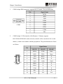
EC51712CLDNA(B) 1 Chapter 1 Product Introduction Typical Power Consumption CPU: Intel® Celeron® M 1.0GHz 400MHz Memory: DDRII533 1GB KingMAX Ø +5V@ 1.01 A; +5%/3%; Ø +3.3V@ 0.6 A; +5%/3%; Ø +12V@ 0.33 A; +5%/3%. Microprocessor Support Intel® Celeron® M 1GHz 400MHz FSB CPU or Intel® Pentium® M 1.8GHz 400MHz FSB CPU. Chipset Intel® 910GMLE + Intel® ICH6M System Memory Support SODIMM DDRII 400MHz memory, up to 1GB. Video Function System integrated video chip, supports VGA and LVDS display modes, LVDS supports up to 24bit dualchannel. Network Function One 10/100/1000Mbps network interface, supports WakeOnLAN function. Audio Function One standard AC´97 sound effect chip, provides excellent sound effect, supports MICin/Linein/Speakerout.
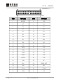
2 EC51712CLDNA(B) Chapter 1 Product Introduction Expansion Bus One PCI golden finger, compatible with PCIMG 1.0 standard; provide one Mini PCI 1.0 slot. CF Card Standard TYPE I and TYPE II CF card, meet more expansion requirements of users. Power Feature AT/ATX power, support single 12V optional configuration. Watchdog Function Ø 255 levels, programmable, by minute or second; Ø Support watchdog overtime or reset system. I/O Interfaces Ø One parallel port; Ø Six serial ports, and COM2 supports RS232/RS422/RS485 mode selection; Ø One IDE interface; Ø Two SATA interfaces; Ø Four USB2.0 interfaces; Ø One PS/2 keyboard/mouse interface; Ø One 8bit digital I/O interface;
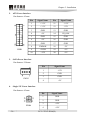
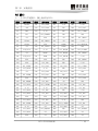
EC51712CLDNA(B) 3 Chapter 2 Installation Chapter 2 Installation Product Outline 5.00
136.00
146.00
LCDB1
5.00
193.00
203.00 Unit: mm
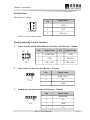
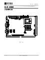
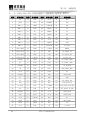
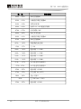
4 EC51712CLDNA(B) Chapter 2 Installation Locations of Interfaces LPT1
PWR1
SATA1 SATA2
IDE1
GPIO1
KM1
JATX1 JCF1
FP3
FP2
FP1 JP1
PWR4
PWR2
PWR3
USB1
COM1
USB2
JP2
JP3
JP4
JCC1
JP5
JP6 COM2
CPUFAN1
VGA1
LAN1
COM6
COM4
COM5
COM3
LVDS1
VGA2
LVDS2
JLCD1
AUDIO1
LCDB1
PCI1
Front View CF1 MPCI1
DIMM1
Rear View
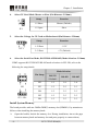
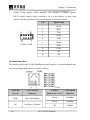
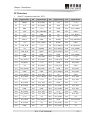
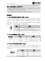
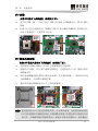
EC51712CLDNA(B) 5 Chapter 2 Installation Motherboard Structure EC51712CLDNA(B) Function Block Diagram Celeron M Dothan 1.0G/512K Processor AGTL+ Bus FSB 400Mhz CRT CH7308B GMCH CH A 910GMLE SDVO DDR2 SODIMM1 DDR Term. D M I LVDS(48BIT) CRT SATA1,2 PCIE PORT1 RTL8111C SATA 1个 USB Pin header USB 2.0 IDE 40Pin IDE IDE Compact Flash Socket 2个 USB PORT ICH6M AC'97 AC'97 PCA9534 SMBUS PCI BUS 8BIT GPIO PCI金手指
FWH BIOS Hardware Monitor LPC L P C Mini PCI
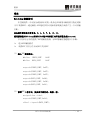
LPC LPC Super I/O W83627DHG COM2(RS232/422/485) COM1 LPT PS/2 6 F81216D COM3/COM4/C0M5/COM6 EC51712CLDNA(B) RJ45 CONNECTOR Chapter 2 Installation Tip: How to identify the first pin of the jumpers and interfaces 1. Observe the letter beside the socket, it would be marked with “1” or thickened lines or triangular symbols; 2. Observe the solder pad on the back, the square pad is the first pin; 3. The red line on the cable or other marks shows that they should be connected with the first pin of the socket. Jumper Settings 1. JCC1: Clear/Save the content of CMOS (Pin Distance: 2.54mm) CMOS is powered by the button battery on board. Clear CMOS will restore original settings (factory default). The steps are listed as follows : (1) Turn off the computer and unplug the power cable; (2) Instantly short circuit JCC1; (3) Turn on the computer; (4) Follow the prompt on screen to enter BIOS setup when starting the computer, load optimized defaults; (5) Save and exit. JCC1 2. Function 12 Open Normal Status (Default) 12 Short Clear CMOS, all the BIOS setup recovers to factory default. JATX1: Select the Power Type (Pin Distance: 2.54mm) JATX1 3. Setup Setup Function 12 Short ATX Power (Default) 23 Short AT Power and Single 12V Power JLCD1: Select LCD Operating Voltage (Pin Distance: 2.54mm) Different LCD screens have different voltages; the board provides two voltage options, 3.3V and 5V. Only when the selected LCD voltage is in accord with the LCD voltage in use, the LCD screen could display normally. Please set it as follows: JLCD1 Setup Function 12 Short +3.3V (Default) 23 Short +5V
EC51712CLDNA(B) 7 Chapter 2 Installation 4. Select CF Card Mode, Master or Slave (Pin Distance: 2.54mm) JP1 5. Setup Function 12 Short Master (Default) 12 Open Slave Select the Voltage for CF Card on Motherboard (Pin Distance: 2.54mm) JCF1 6. Setup Function 12 Short +3.3V 23 Short +5V (Default) Select the Serial Port Mode, RS232/RS422/RS485 (Mode Selection: 2.54mm) COM2 supports RS232/RS422/RS485 mode selection via JP2~JP6, refer to the following for setup details: Mode Selection Pin Setup RS232 (Default) JP2 RS422 RS485 JP2 12 56 34 JP3 12 23 23 JP4 12 23 23 JP5 12 23 23 JP6 12 23 23 JP3~JP6 Install System Memory The board provides with one 200Pin DDRⅡ memory slot (DIMM1). Pay attention as follows when installing the memory bank: Ø Open the buckles beside the memory slot. During installation, aim at the gaps between memory bank and memory slot and press properly to connect them;
8 EC51712CLDNA(B) Chapter 2 Installation Ø Support DDRⅡ 400MHz memory; memory capacity shall not exceed 1GB. Ø It is recommended to use DIMM memory with SPD to ensure stable operation. Video Interface 1. This board provides one standard DB15 interface. The pin definitions are listed as follows: Pin Signal Name Pin Signal Name 1 Red 2 Green 3 Blue 4 NC 5 GND 6 GND 7 GND 8 GND 9 +5V 10 GND 11 NC 12 DDCDATA 13 HSYNC 14 VSYNC 15 DDCCLK VGA1 2. This board provides one standard 2x8PIN interface (Pin Distance: 2.54mm), VGA device needs to be connected via transfer cable. The pin definitions are listed as follows: VGA2 Pin Signal Name Pin Signal Name 1 Red 2 GND 3 NC 4 Green 5 GND 6 DDCDATA 7 Blue 8 GND 9 HSYNC 10 NC 11 +5V 12 VSYNC 13 GND 14 GND 15 DDCCLK 16 shield_gnd
EC51712CLDNA(B) 9 Chapter 2 Installation 3. 24bit Dualchannel LVDS Connector (Pin Distance: 1.0mm) LVDS connector supports 18/24bit dualchannel or singlechannel LCD screen. Singlechannel can only adopts LVDS1 connector and the corresponding options are required to be set in CMOS. LVDS1 LVDS2 Pin Signal Name Pin Signal Name 1 LVDSO_D0+ 2 LVDSO_D0 3 GND 4 GND 5 LVDSO_D1+ 6 LVDSO_D1 7 GND 8 GND 9 LVDSO_D2+ 10 LVDSO_D2 11 GND 12 GND 13 LVDSO_CLK+ 14 LVDSO_CLK 15 GND 16 GND 17 LVDSO_D3+ 18 LVDSO_D3 19 VDD 20 VDD Pin Signal Name Pin Signal Name 1 LVDSE_D0+ 2 LVDSE_D0 3 GND 4 GND 5 LVDSE_D1+ 6 LVDSE_D1 7 GND 8 GND 9 LVDSE_D2+ 10 LVDSE_D2 11 GND 12 GND 13 LVDSE_CLK+ 14 LVDSE_CLK 15 GND 16 GND 17 LVDSE_D3+ 18 LVDSE_D3 19 VDD 20 VDD Note: LVDSOx represents dualscanning the odd line of PANEL; LVDSEx represents dualscanning the even line of PANEL.
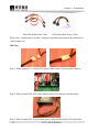
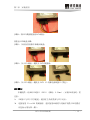
10 EC51712CLDNA(B) Chapter 2 Installation LCD Backlight Control Interface Pin distance: 2.0mm. LCDB1 Pin Signal Name 1 +12V 2 NC 3 LCD_BKLTEN 4 GND Note: the current of Pin 1 is less than 1A; LCD_BKLTEN Backlight enabling, active high. SATA Interface This board provides two SATA interfaces. The pin definitions are listed as follows: Pin SATA1/SATA2 Signal Name 1 GND 2 TX+ 3 TX 4 GND 5 RX 6 RX+ 7 GND Hotswap of SATA Hard Disk Notices for Hotswap of SATA Hard Disk 1. The hard disk shall support SATA 2.0 and use 15 pin SATA hard disk power. 2. The driver of chipset shall support the hotswap SATA hard disk. 3. Hotswap of SATA hard disk with the operating system is forbidden when system is poweron.
EC51712CLDNA(B) 11 Chapter 2 Installation SATA Hard Disk Data Cable SATA Hard Disk Power Cable
Please carry out hot plug as follows, improper operation may destroy the hard disk or result in data lost. Hot Plug Step 1: Please plug the 1 x 4 pin SATA power cable (white) into the power adapter. Step 2: Please connect the SATA data cable to the SATA interface on the board. Step 3: Please connect the 15pin SATA power cable (black) to the SATA hard disk. 12 EC51712CLDNA(B) Chapter 2 Installation Step 4: Please connect the SATA data cable to the SATA hard disk. Hot Unplug Step 1: Unplug the data cable from the SATA hard disk. Step 2: Unplug the SATA 15pin power cable (black) from the SATA hard disk. IDE Interface This board provides a set of 40pin IDE interface (IDE1) (Pin Distance: 2.54mm), please pay attention as follows when installing the IDE device: Ø IDE interface shares channel with CF card and the “Master/Slave” setup shall be corresponding with that of CF card.
EC51712CLDNA(B) 13 Chapter 2 Installation Ø When using an Ultra 100 hard disk, it is recommended to use 80pin appropriative flat cable (the Pin 1 of IDE cable is marked with red sign). IDE1 14 Pin Signal Name Pin Signal Name 1 RESET# 2 GND 3 D7 4 D8 5 D6 6 D9 7 D5 8 D10 9 D4 10 D11 11 D3 12 D12 13 D2 14 D13 15 D1 16 D14 17 D0 18 D15 19 GND 20 Key 21 DREQ 22 GND 23 IOW# 24 GND 25 IOR# 26 GND 27 IORDY 28 GND 29 DACK# 30 GND 31 IRQ 32 NC 33 DA1 34 ATA66_DET 35 DA0 36 DA2 37 CS1# 38 CS3# 39 LED# 40 GND
EC51712CLDNA(B) Chapter 2 Installation USB Interface This board provides two sets of USB interfaces, which can connect with four standard USB devices. USB1 provides two standard USB sockets, USB2 is a 2x5Pin USB pinstyle connector (Pin Distance: 2.54mm). USB2 needs transfer cable to connect the signals to the standard USB socket. The pin definitions are listed as follows: USB1 USB2 Pin Signal Name 1 +5V 2 USB_Data 3 USB_Data+ 4 GND Pin Signal Name Pin Signal Name 1 +5V 2 +5V 3 USB1_Data 4 USB2_Data 5 USB1_Data+ 6 USB2_Data+ 7 GND 8 GND 9 NA 10 GND_CHASSIS Keyboard/Mouse Interface KM1 Pin Signal Name 1 KB_DATA 2 MS_DATA 3 GND 4 +5V 5 KB_CLK 6 MS_CLK
EC51712CLDNA(B) 15 Chapter 2 Installation Parallel Port This board provides one 2x13Pin slot for parallel port (Pin Distance: 2.54mm), transfer cable is needed to fix it to the chassis, so that it can connect with the peripherals. The pin definitions are listed as follows: LPT1 Pin Signal Name Pin Signal Name 1 STB# 2 AFD# 3 PD0 4 ERR# 5 PD1 6 INIT# 7 PD2 8 SLIN# 9 PD3 10 GND 11 PD4 12 GND 13 PD5 14 GND 15 PD6 16 GND 17 PD7 18 GND 19 ACK# 20 GND 21 BUSY 22 GND 23 PE 24 GND 25 SLCT 26 NC Serial Port This board provides six serial ports, and COM2 supports RS232/RS422/RS485 mode selection, COM3~COM6 support RS232 mode.
16 EC51712CLDNA(B) Chapter 2 Installation 1. COM1 adopts DB9 connector, supports RS232 mode. The pin definitions: COM1 2. Pin Signal Name 1 DCD# 2 RXD 3 TXD 4 DTR# 5 GND 6 DSR# 7 RTS# 8 CTS# 9 RI# COM2 adopts 2×5Pin interface (Pin Distance: 2.54mm), supports RS232/RS422/RS485 mode selection, transfer cable is needed to fix it to the chassis, so that it can connect with the peripherals. The pin definitions are listed as follows: Signal Name Pin COM2 RS232 RS422 RS485 1 DCD# TXD Data 2 RXD TXD+ Data+ 3 TXD RXD+ X 4 DTR# RXD X 5 GND GND GND 6 DSR# X X 7 RTS# X X 8 CTS# X X 9 RI# X X 10 NA NA NA
EC51712CLDNA(B) 17 Chapter 2 Installation 3. COM3~COM6 adopts 2×5Pin interface (Pin Distance: 2.54mm), support RS232 mode, transfer cable is needed to fix it to the chassis, so that it can connect with the peripherals. The pin definitions are listed as follows: COM3~COM6 Pin Signal Name 1 DCD# 2 RXD 3 TXD 4 DTR# 5 GND 6 DSR# 7 RTS# 8 CTS# 9 RI# 10 NA Network Interface This board provides one 10/100/1000Mbps network interface. Its pin arrangement and the corresponding input socket are listed as follows: LAN1 ACTLED LAN Activity LILED LAN Speed (Green) Indicator (DualColor: Y/G) Indicator Flash Data Transmitting Green 1000Mbps Yellow 100Mbps Off No Data to Transmit Off 10Mbps
18 EC51712CLDNA(B) Chapter 2 Installation Audio Interface Lout can be connected to earphone or more suitable power loudspeaker via the cable attached to the motherboard. Lin is used for the computer to record the tape station or other sound sources, or play via Lout. Mic is used to connect the input sound of microphone. (Pin Distance: 2.54mm) Pin Signal Name Pin Signal Name 1 LOUT_R 2 LOUT_L 3 GND_AUDIO 4 GND_AUDIO 5 LIN_R 6 LIN_L 7 GND_AUDIO 8 GND_AUDIO 9 MIC_IN 10 MIC_P AUDIO1 Digital I/O Interface This board provides a GPIO interface with 4channel input while the other 4 channels for output. (Pin Distance: 2.54mm). GPIO1 Pin Signal Name Pin Signal Name 1 INPUT1 2 OUTPUT1 3 INPUT2 4 OUTPUT2 5 INPUT3 6 OUTPUT3 7 INPUT4 8 OUTPUT4 9 GND 10 +5V Pin Signal Name 1 +12V 2 GND 3 GND 4 +5V
Power Interface 1. AT Power Interface Pin distance: 5.08mm. PWR2 EC51712CLDNA(B) 19 Chapter 2 Installation 2. ATX Power Interface Pin distance: 4.2mm. Pin Signal Name Pin Signal Name 1 +3.3V 11 +3.3V 2 +3.3V 12 12V 3 GND 13 GND 4 +5V 14 PS_ON# 5 GND 15 GND 6 +5V 16 GND 7 GND 17 GND 8 PWROK 18 5V 9 +5VSB 19 +5V 10 +12V 20 +5V PWR1 3. SATA Power Interface Pin distance: 2.54mm. PWR3 Pin Signal Name 1 +12V 2 GND 3 GND 4 +5V 4. Single 12V Power Interface Pin distance: 4.2mm. PWR4 20 Pin Signal Name 1 GND 2 GND 3 +12V 4 +12V
EC51712CLDNA(B) Chapter 2 Installation Fan Interface Pin distance: 2.54mm. Pin Signal Name 1 GND 2 +12V 3 FAN_IO CPUFAN1 FAN_IO: Fan rev pulse output Status Indicating Control Interface 1. Power Switch and Hard Disk Indicator Interface (Pin Distance: 2.54mm) FP1 Pin Signal Name Pin Signal Name 1 PWRBTN# 2 GND 3 GND 4 RESET# 5 IDE_LED 6 IDE_LED+ 2. Power Indicator Interface (Pin Distance: 2.54mm) FP2 Pin Signal Name 1 PWR_LED+ 2 NC 3 GND 3. Loudspeaker Output Interface (Pin Distance: 2.54mm) FP3 Pin Signal Name 1 SPEAKER 2 NC 3 GND 4 +5V
EC51712CLDNA(B) 21 Chapter 2 Installation CF Card Compact Flash card is a sort of high speed memory, small in size and easy to use. Its storage capacity will vary with different cards in use, such as 128M, 256M, etc. CF card could only be inserted in one direction and it is marked as CF1. 22 Pin Signal Name Pin Signal Name 1 GND 26 CD1# 2 D3 27 D11 3 D4 28 D12 4 D5 29 D13 5 D6 30 D14 6 D7 31 D15 7 CS0# 32 CS1# 8 GND 33 VS1# 9 ATASEL# 34 IOR# 10 GND 35 IOW# 11 GND 36 WE# 12 GND 37 IRQ 13 VCC 38 VCC 14 GND 39 CSEL# 15 GND 40 VS2# 16 GND 41 RESET# 17 GND 42 IORDY 18 A2 43 DREQ 19 A1 44 DACK# 20 A0 45 DASP# 21 D0 46 ATA66_DET 22 D1 47 D8 23 D2 48 D9 24 WP/IOCS16# 49 D10 25 CD2# 50 GND
EC51712CLDNA(B) Chapter 2 Installation PCI Interface 1. One PCI expansion interface, PCI1. Pin Signal Name Pin Signal Name Pin Signal Name Pin A1 TRST# A31 PCI_AD18 B1 12V B31 +3.3V A2 +12V A32 PCI_AD16 B2 TCK B32 PCI_AD17 A3 TMS A33 +3.3V B3 GND B33 PCI_C/BE#2 A4 TDI A34 PCI_FRAME# B4 TDO B34 GND A5 +5V A35 GND B5 +5V B35 PCI_IRDY# A6 INTA# A36 PCI_TRDY# B6 +5V B36 +3.3V A7 INTC# A37 GND B7 INTB# B37 PCI_DEVSEL# A8 +5V A38 PCI_STOP# B8 INTD# B38 GND A9 CLK_PCI2 A39 +3.3V B9 PCI_REQ3# B39 PCI_PLOCK# A10 +5V A40 SDONE B10 PCI_REQ1# B40 PCI_PERR# A11 CLK_PCI3 A41 SBO# B11 PCI_GNT3# B41 +3.3V A12 GND A42 GND B12 GND B42 PCI_SERR# A13 GND A43 PCI_PAR B13 GND B43 +3.3V A14 PCI_GNT1# A44 PCI_AD15 B14 CLK_PCI0 B44 PCI_C/BE#1 A15 PCI_RST# A45 +3.3V B15 GND B45 PCI_AD14 A16 +5V A46 PCI_AD13 B16 CLK_PCI1 B46 GND A17 PCI_GNT0# A47 PCI_AD11 B17 GND B47 PCI_AD12 A18 GND A48 GND B18 PCI_REQ0# B48 PCI_AD10 A19 PCI_REQ2# A49 PCI_AD9 B19 +5V B49 GND A20 PCI_AD30 A50 PCI_C/BE#0 B20 PCI_AD31 B50 PCI_AD8 A21 +3.3V A51 +3.3V B21 PCI_AD29 B51 PCI_AD7 A22 PCI_AD28 A52 PCI_AD6 B22 GND B52 +3.3V A23 PCI_AD26 A53 PCI_AD4 B23 PCI_AD27 B53 PCI_AD5 A24 GND A54 GND B24 PCI_AD25 B54 PCI_AD3 A25 PCI_AD24 A55 PCI_AD2 B25 +3.3V B55 GND A26 PCI_GNT2# A56 PCI_AD0 B26 PCI_C/BE#3 B56 PCI_AD1 A27 +3.3V A57 +5V B27 PCI_AD23 B57 +5V A28 PCI_AD22 A58 PCI_REQ64 B28 GND B58 PCI_ACK64# A29 PCI_AD20 A59 +5V B29 PCI_AD21 B59 +5V A30 GND A60 +5V B30 PCI_AD19 B60 +5V
EC51712CLDNA(B) Signal Name 23 Chapter 2 Installation 2. One 124Pin MiniPCI expansion bus interface (on the rear of board, MPCI1). Pin Signal Name 1 TIP Pin Signal Name Pin Signal Name Pin 32 2 RING 3 8PMJ3 4 5 GND 63 33 AD31 34 PME# 8PMJ1 35 8PMJ6 36 6 8PMJ2 7 8PMJ7 8 8PMJ4 9 8PMJ8 10 Signal Name +3.3V 94 AD2 64 FRAME# 95 AD3 65 CLKRUN# 96 AD0 AD29 66 TRDY# 97 +5V NC 67 SERR# 98 NC 37 GND 68 STOP# 99 AD1 38 AD30 69 GND 100 NC 39 AD27 70 +3.3V 101 GND 40 +3.3V 71 PERR# 102 GND 8PMJ5 41 AD25 72 DEVSEL# 103 AC_SYNC 11 LED1_GRNP 42 AD28 73 C/BE1# 104 M66EN 12 LED2_YELP 43 NC 74 GND 105 AC_SDATA_IN 13 LED1_GRNN 44 AD26 75 AD14 106 AC_SDATA_OUT 14 LED2_YELN 45 C/BE3# 76 AD15 107 AC_BIT_CLK 15 CHSGND 46 AD24 77 GND 108 AC_CODEC_ID0# 16 NC 47 AD23 78 AD13 109 AC_CODEC_ID1# 17 PIRQB# 48 IDSEL 79 AD12 110 AC_RESET# 18 +5V 49 GND 80 AD11 111 MOD_AUDIO_MON 19 +3.3V 50 GND 81 AD10 112 NC 20 PIRQA# 51 AD21 82 GND 113 AUDIO_GND 21 NC 52 AD22 83 GND 114 GND 22 NC 53 AD19 84 AD9 115 SYS_AUDIO_OUT 23 GND 54 AD20 85 AD8 116 SYS_AUDIO_IN 24 +3.3AUX 55 GND 86 C/BE0# 117 SYS_AUDIO_OUT_GND 25 CLK 56 PAR 87 AD7 118 SYS_AUDIO_IN_GND 26 RESET# 57 AD17 88 +3.3V 119 AUDIO_GND 27 GND 58 AD18 89 +3.3V 120 AUDIO_GND 28 +3.3V 59 C/BE2# 90 AD6 121 NC 29 REQ# 60 AD16 91 AD5 122 MPCIACT# 30 GNT# 61 IRDY# 92 AD4 123 +5V 31 +3.3V 62 GND 93 NC 124 +3.3AUX
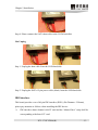
24 EC51712CLDNA(B) Chapter 2 Installation Install CPU Please install the CPU as follows (See the figure below): Ø Ø Aim the first pin of the CPU (with triangular symbol) with the gap on the CPU socket and insert the CPU into the socket. After the CPU is installed properly, tighten the screws on the CPU socket in clockwise direction via screwdriver. Pay attention to the strength and do not destroy the CPU socket. Install CPU Fan Please install the CPU fan as follows: (See the figure below): Ø Firstly, aim the backplane of the cooling fin (see figure ④) with the fixing holes on the rear of the CPU card; Ø Connect the cooling fin (see figure ⑤) with the backplane in the front and fix them; pay attention that the surface between the cooling fin and the CPU crystal wafer is well contacted; Ø Fix the cooling fin with two screws on the cross (do not tighten it) and then the other two screws; then tighten the four screws; Ø Lastly, connect the fan power cable onto the fan socket on the CPU card. Note! It is recommended to use cooling fan authenticated by Intel; before installing the fan, smear the heat sink compound on the surface between CPU and the fan cooling fin to improve the heat dissipation performance; always check whether the fan is operating normally to ensure the heat dissipation within the chassis. When holding a board, please hold the edge instead of the cooling fin.
EC51712CLDNA(B) 25 Chapter 3 BIOS Setup Chapter 3 BIOS Setup BIOS Overview BIOS (Basic Input and Output System) is solidified in the flash memory on the CPU board. Its main functions include: initialize system hardware, set the operating status of the system components, adjust the operating parameters of the system components, diagnose the functions of the system components and report failures, provide hardware operating and controlling interface for the upper level software system, guide operating system and so on. BIOS provides users with a humancomputer interface in menu style to facilitate the configuration of system parameters for users, control power management mode and adjust the resource distribution of system device, etc. Setting the parameters of the BIOS correctly could enable the system operating stably and reliably; it could also improve the overall performance of the system at the same time. Inadequate even incorrect BIOS parameter setting will decrease the system operating capability and make the system operating unstably even unable to operate normally. BIOS Parameter Setup Prompt message for BIOS setting may appear once powering on the system. At that time (inefficient at other time), press the key specified in the prompt message (usually <Del>) to enter BIOS setting. When the BIOS setting in CMOS is destroyed, system may also require entering BIOS setting or selecting certain default value. All the setup values modified by BIOS are saved in the CMOS storage in system. The CMOS storage is powered by battery; unless clearing CMOS contents, or else its contents will not be lost even if powered off. Note! BIOS setting will influent the computer performance directly. Setting parameter improperly will cause damage to the computer; it may even unable to power on. Please use the internal default value of BIOS to restore the system. Our company is constantly researching and updating BIOS, its setup interface may be a bit different. The figure below is for reference only; it may be different from your BIOS setting in use.
26 EC51712CLDNA(B) Chapter 3 BIOS Setup BIOS Basic Function Setup After starting SETUP program, you may see the main interface of CMOS Setup Utility as follows: BIOS SETUP UTILITY System Overview Processor CPU Type : Intel(R) Celeron® M processor 1.0GHz Speed :1.0GHz System Memory Size: 248MB ←→ Select Screen ↑↓ Select Item + Change Field Tab Select Field F1 General Help F10 Save and Exit ESC Exit Power Supply Type :AT System Time System Date [00:47:55] [Wed 01/02/2002] V02.57 (c)Copyright 19852004,American Megatrends, Inc. 1. Main (1) System Time Select this option and set the current time by < + > / < >, which is displayed in format of hour/minute/second. Reasonable range for each option is: Hour (0023), Minute (0059), Second (0059). (2) System Date Select this option and set the current data by < + > / < >, which is displayed in format of month/date/year. Reasonable range for each option is: Month (Jan.Dec.), Date (0131), Year (Maximum to 2099), Week (Mon. ~ Sun.).
EC51712CLDNA(B) 27 Chapter 3 BIOS Setup 2. Advanced BIOS SETUP UTILITY Configure CPU Advanced Settings WARNING:Setting wrong values in below sections may cause system to malfunction ←→ Select Screen ↑↓ Select Item Enter Go to Sub Screen Tab Select Field F1 General Help F10 Save and Exit ESC Exit „CPU Configuration „IDE Configuration „SuperIO Configration „Hardware Health Configuration „USB Configuration „Power Management Configuration „Clock Generator Configuration V02.57 (c)Copyright 19852004,American Megatrends, Inc. (1) CPU Configuration BIOS SETUP UTILITY Configure advanced CPU settings Module Version – 11.05 Manufacturer: Intel Brand String: Intel(R) Celeron® M processor 1.0GHz Frequency; : 1.0GHz FSB Speed; :400MHz Cache L1; :32 KB Cache L2; :512 KB ←→ Select Screen ↑↓ Select Item + Change Field Tab Select Field F1 General Help F10 Save and Exit ESC Exit V02.57 (c)Copyright 19852004,American Megatrends, Inc.
28 EC51712CLDNA(B) Chapter 3 BIOS Setup (2) IDE Configuration BIOS SETUP UTILITY IDE Configuration ATA/IDE Configuration [enhanced] „Primary IDE Master „Primary IDE Slave „Secondary IDE Master „Secondary IDE Slave „Third IDE Master „Third IDE Slave :[Not Detected] :[Not Detected] :[Not Detected] :[Not Detected] :[Not Detected] :[Not Detected] ←→ Select Screen ↑↓ Select Item + Change Field Tab Select Field F1 General Help F10 Save and Exit ESC Exit V02.57 (c)Copyright 19852004,American Megatrends, Inc. ① ATA/IDE Configuration There are three options for this item, Disabled, Compatible and Enhanced. Compatible mode could map the SATA hard disk interface to the corresponding interface on the parallel IDE channel. ② Legacy IDE Channels There are three options, SATA Only; SATA Pri, PATA Sec and PATA Only to set IDE channel. ③ Primary, Secondary, Third IDE Master/Slave a) Type Not Installed: system has not detected IDE device. AUTO: automatic detection of IDE parameters when power on; CD/DVD: used for ATAPI CDROM; ARMD: used for various analog IDE devices. b) LBA/Large Mode Used to set whether to support LBA mode. c) Block (Multisector Transfer) Used to set whether to support multisector simultaneous transfer or not.
EC51712CLDNA(B) 29 Chapter 3 BIOS Setup d) PIO Mode Used to set PIO mode. e) DMA Mode Used to set DMA mode. f) S.M.A.R.T This option is used to set whether to enable hard disk S.M.A.R. function, can only be applied to the hard disk that supports this function. g) 32Bit Data Transfer This option is used to enable the 32bit hard disk access mode, which will optimize the read and write speed of hard disk. (3) Super IO Configuration BIOS SETUP UTILITY Floppy A [Disabled] OnBoard Floppy Controller [Enabled] Serial Port1 Address Serial Port2 Address [3F8/IRQ4] [2F8/IRQ3] Serial Port3 Address [200] Serial Port3 IRQ [10] Serial Port4 Address [208] Serial Port4 IRQ [10] Serial Port2 Address [210] Serial Port5 IRQ [10] Serial Port6 Address [218] Serial Port6 IRQ [10] Parallel Port Address [378] Parallel Port Mode [Normal] Parallel Port IRQ [IRQ7] Allows BIOS to Enable or Disable Floppy Controller. ←→ Select Screen ↑↓ Select Item + Change Field Tab Select Field F1 General Help F10 Save and Exit ESC Exit V02.57 (c)Copyright 19852004,American Megatrends, Inc. ① Floppy A This options is used to configure floppy driver, the default value is “Disabled”.
30 EC51712CLDNA(B) Chapter 3 BIOS Setup ② Onboard Floppy Controller This option is used to configure the floppy driver controller; the default value is “Enabled”. ③ Serial Port 16 Address This option is used to set the address of serial port 1~6 on the motherboard. ④ Serial Port 36 IRQ This option is used to set the IRQ of serial port 3~6. ⑤ Parallel Port Address This option is used to set the address of parallel port on the motherboard, the default value is 378. ⑥ Parallel Port Mode This option is used to set the operating mode of the parallel port, Normal, BiDirectional, ECP, EPP. EPP represents the maximum speed under bidirectional data transmission; and ECP represents a faster speed than EPP under bidirectional data transmission. ⑦ Parallel Port IRQ This option is used to set the IRQ of the parallel port on motherboard. (4) Hardware Health Configuration BIOS SETUP UTILITY Enables Hardware Health Monitoring Device Hardware Health Configuration System Temperature : 33℃/138℉ CPU Temperature : 34℃/120℉ CPUFAN1 Speed :N/A Vcore V3.3 V5.0 V12.0 VBAT : 0.929 V : 3.298V :5.041 V :12.294V : 3.148 V ←→ Select Screen ↑↓ Select Item + Change Field Tab Select Field F1 General Help F10 Save and Exit ESC Exit V02.57 (c)Copyright 19852004,American Megatrends, Inc.
EC51712CLDNA(B) 31 Chapter 3 BIOS Setup ① System Temperature The current system temperature, typically, there is thermosensitive resistor monitor on motherboard. ② CPU Temperature The current CPU temperature, it is monitored by the temperature sensor on board. ③ CPUFAN Speed The current rev of CPU and system fan. ④ Vcore CPU core voltage. ⑤ V3.3/V5.0/V12.0 The output voltage of switch. ⑥ VBAT Battery Voltage. (5) USB Configuration USB Configuration BIOS SETUP UTILITY Enables USB host controllers. Module Version 2.24.011.4 USB Devices Enabled : Legacy USB Support ←→ Select Screen ↑↓ Select Item + Change Field F1 General Help [4 USB Ports] F10 Save and Exit ESC Exit [Enabled] USB 2.0 Controller [Enabled] None USB Function V02.57 (c)Copyright 19852004,American Megatrends, Inc. ① USB Function This option is used to set the number of USB controller, confirming how many controllers will be supported; typically, one controller support two USB interfaces.
32 EC51712CLDNA(B) Chapter 3 BIOS Setup ② Legacy USB Support Support traditional USB keyboard and mouse, when this option is set to be “Enabled”, USB device is available even under the operating system that does not support USB such as DOS. ③ USB 2.0 Controller This option is used to select whether to support USB2.0 controller. (6) Power Management Configuration BIOS SETUP UTILITY ACPI Settings ACPI Aware O/S [YES] Resume On RTC Alarm [Disabled] ←→ Select Screen ↑↓ Select Item + Change Field F1 General Help F10 Save and Exit ESC Exit V02.57 (c)Copyright 19852004,American Megatrends, Inc. ① ACPI Aware O/S This option is used to set whether the OS is ACPI or APM. (7) Clock Generator Configuration BIOS SETUP UTILITY Clock Generator Configuration Spread Spectrum : [Enabled] Auto PCI Clock : [Enabled] ←→ Select Screen ↑↓ Select Item + Change Field F1 General Help F10 Save and Exit ESC Exit V02.57 (c)Copyright 19852004,American Megatrends, Inc.
EC51712CLDNA(B) 33 Chapter 3 BIOS Setup ① Spread Spectrum This option is used to set whether to support spread spectrum function. ② Auto PCI Clock This option is used to set whether to support disabling function of unused clock. 3. Chipset BIOS SETUP UTILITY Advanced Chipset Settings WARNING:Setting wrong values in below sections may cause system to malfunction. NorthBridge Configuration DRAM Frequency [Auto] Configure DRAM Timing by SPD [Enabled] Boots Graphic Adapter Priority [PEG/PCI] Internal Graphics Mode Select [Enabled,8MB] Boot Display Device [CRT] SDVO Flat Panel Type [1024×768LVDS] SDVO Panel Connector [SPWG] LVDS Channel [Dual channel] Panel Color Depth [24bit color depth] ←→ Select Screen ↑↓ Select Item Enter Go to Sub Screen F1 General Help F10 Save and Exit ESC Exit SouthBridge Configuration Onboard Audio controller [enabled] V02.57 (c)Copyright 19852004,American Megatrends, Inc.
34 EC51712CLDNA(B) Chapter 3 BIOS Setup (1) RAM Frequency Configure the frequency of DRAM. (2) Configure DRAM Timing by SPD BIOS configures the SDRAM timing according to the content in SPD. There is a little chip on most of the memory stick for holding the memory timing and capacity parameter, i.e. SPD chip. (3) Boots Graphic Adapter Priority Select the priority of graphic adapter. (4) Internal Graphics Mode Select The graphic adapter applies a appropriative system address space for graphic memory address space. (5) Boot Display Device Select the type of boot device. (6) SDVO Flat Panel Type Select the resolution of LVDS. (7) SDVO Panel Connector Select the connector type of LVDS. (8) LVDS Channel Select the channel of LVDS, dualchannel or singlechannel. (9) Panel Color Depth Select the color depth of panel. (10) Onboard Audio Controller Select whether to turn on audio card controller.
EC51712CLDNA(B) 35 Chapter 3 BIOS Setup 4. PCIPnP BIOS SETUP UTILITY Advanced PCI/PnP Settings WARNING:Setting wrong values in below sections may cause system to malfunction. IRQ3 [Available] IRQ4 [Available] IRQ5 [Available] IRQ7 [Available] IRQ9 [Available] IRQ10 [Available] IRQ11 [Available] IRQ14 [Available] IRQ15 [Available] ←→ Select Screen ↑↓ Select Item + Change Field F1 General Help F10 Save and Exit ESC Exit V02.57 (c)Copyright 19852004,American Megatrends, Inc. (1) IRQ 3~15 This option is used to specify the IRQ interrupt mode, PNP mode or reserved for ISA. 5. Boot BIOS SETUP UTILITY Boot Settings Quick Boot [Enabled] Quiet Boot [Disabled] Waite For ‘F1’ If Error [Enabled] Boot Device Priority 1 st Boot Device ←→ Select Screen ↑↓ Select Item Enter Go to Sub Screen F1 General Help F10 Save and Exit ESC Exit [ ] V02.57 (c)Copyright 19852004,American Megatrends, Inc.
36 EC51712CLDNA(B) Chapter 3 BIOS Setup (1) Quick Boot Configure whether to permit skipping certain test during BIOS boot to reduce BIOS booting time. (2) Quiet Boot Configure whether to display the content of OEM LOGO. (3) Wait for ‘F1’ If Error Configure whether to prompt pressing “F1” if error. (4) 1 st ~4 th Boot Device Configure the preference of the startup sequence for devices when the system starts. 6. Security BIOS SETUP UTILITY Security Settings Supervisor Password :Not Installed User Password :Not Installed Change Supervisor Password Change User Password Install or Change the password ←→ Select Screen ↑↓ Select Item Enter Change F1 General Help F10 Save and Exit ESC Exit V02.57 (c)Copyright 19852004,American Megatrends, Inc. (1) Change User/ Supervisor Password After pressing Change User/ Supervisor Password and input new password in the dialog box, this column will indicate that user’s password has been installed.
EC51712CLDNA(B) 37 Chapter 3 BIOS Setup 7. Exit South Bridge Configuration Exit Options Exit system setup after saving the changes. Save Changes and Exit Discard Changes and Exit ←→ Select Screen ↑↓ Select Item Enter Go to Sub Screen F1 General Help F10 Save and Exit ESC Exit Discard Changes Load Optimal Defaults Load Failsafe Defaults V02.57 (c)Copyright 19852004,American Megatrends, Inc. (1) Save Changes and Exit When you have finished all the changes and want to cover the original parameters, you may implement this operation and save the new parameters into CMOS storage. To implement this operation, you may choose this option and press < Enter >; press < Enter > again to exit. (2) Discard Changes and Exit If you do not want to save the change into CMOS storage, please choose this option and press < Enter >; press < Enter > again to exit. (3) Discard Changes If error occurs in your change and need to be neglected, please choose this option and press < Enter > to enter corresponding options again and reconfigure it. (4) Load Optimal Defaults This menu is used to load default value in system configuration. These default values are optimized and could give play to the high capability of all hardware. (5) Load Failsafe Defaults The function of this option is to initialize the setup of each option to realize the most fundamental and secure system functional value. To implement this function, choose this option and press < Enter >; messages to be confirmed will display on the screen, press < Enter > to implement this function.
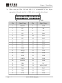
38 EC51712CLDNA(B) Chapter 3 BIOS Setup The System Resources Managed by BIOS under x86 Platform We define three kinds of system resources here: I/O port address, IRQ interrupt number and DMA number. 1. DMA Level Function DMA0 Not Assigned DMA1 Not Assigned DMA2 Not Assigned DMA3 Not Assigned (Sometimes used for hard disk) DMA4 Used for the cascade of DMAC DMA5 Not Assigned DMA6 Not Assigned DMA7 Not Assigned 2. APIC Advanced programmable interrupt controller. Most motherboards above P4 level support APIC and provide more than 16 interrupt sources, like IRQ16 IRQ23; while some others can have up to 28 interrupt sources. However, relevant OS are required to support that function, and currently, only the OS above Windows 2000 could support that function. 3. IO Port Address There are 16 I/O address lines for X86, from 0 ~ 0FFFFh; and there is altogether 64K I/O address space. In traditional ISA interface, only the first 1024 ports are in use (0000~03FFh) and the port number above 0400h are used by PCI interface and EISA
EC51712CLDNA(B) 39 Chapter 3 BIOS Setup interface. Each peripheral device shall occupy a part of the I/O address. The table below lists the I/O interfaces used roughly in X86 platform. Address 000h 00Fh DMA Controller#1 020h 021h Programmable Interrupt Controller#1 040h 043h System Timer 060h 064h Standard 101/102 Keyboard Controller 070h 071h Realtime Clock, NMI 080h 09Fh DMA Page Register 0A0h 0A1h Programmable Interrupt Controller#2 0C0h 0DFh DMA Controller#2 0F0h – 0FFh Numeric Data Processor 1F0h 1F7h Primary IDE 200h – 207h COM3 208h – 20Fh COM4 210h – 217h COM5 218h – 21Fh COM6 274h – 277h PnP Configuration Register Port 279h、A79h PnP Configuration Register Port 2F8h 2FFh COM2 378h 37Fh Parallel Port#1(LPT1) 3B0h 3DFh Display Card Interface 3F6h 3F8h 3FFh 40 Device Description Primary IDE(dual FIFO) COM1
EC51712CLDNA(B) Chapter 3 BIOS Setup 4. IRQ Assignment Table There are 15 interrupt sources in the system. Some are exclusively occupied by the system device. Only the ones which are not exclusively occupied can be distributed. The ISA devices claim to engross the interrupt. Only the plug and play ISA devices can be distributed by the BIOS or the OS. And several PCI devices can share one interrupt through the distribution of BIOS or OS. The diagram below shows parts of the interrupt distribution, but it does not show the interrupts of the PCI devices. Level Function IRQ0 System Timer IRQ1 Standard 101/102 Key or Microsoft Keyboard IRQ2 Reserved IRQ3 COM2 IRQ4 COM1 IRQ5 Reserved IRQ6 Reserved IRQ7 Reserved IRQ8 System CMOS/Realtime Clock IRQ9 Microsoft ACPI Compatible System/AMQZBM50 IDE Controller IRQ10 COM3/4/5/6 IRQ11 Intel (R)82801 FB/FBM SMBus Controller IRQ12 Mouse IRQ13 Reserved IRQ14 Primary IDE
EC51712CLDNA(B) 41 Chapter 4 Install the Drivers Chapter 4 Install the Drivers Please install the drivers of this product according to the content of the equipped CD, it will not be introduced here.
42 EC51712CLDNA(B) Appendix Appendix Watchdog Programming Guide This board provides a programmable watchdog timer (WDT) up to 255 levels. Watchdog timer overtime event can be programmed to reset system or generate maskable interrupts. The available IRQ numbers for this board are: 3, 4, 5, 7, 9, 10 and 11. Before using, please modify the corresponding IRQ number in PCIPnP of BIOS Setup interface into “Reserved”. The following gives an example for WDT programming in C language. The steps to program WDT are listed as follows: Ø Enter WDT programming mode Ø Set WDT operating mode/enable WDT/disable WDT (1) Enter WDT Programming Mode #define INDEX_PORT 0x2E #define DATA_PORT 0x2F outportb(INDEX_PORT, 0x87); outportb(INDEX_PORT, 0x87); outportb(INDEX_PORT, 0x07); outportb(DATA_PORT, 0x08); outportb(INDEX_PORT, 0x30); outportb(DATA_PORT, 0x01); (2) Configure the Operating Mode for WDT, Reset or Interrupt unsigned char oldval; outportb(INDEX_PORT,0x2d); oldval = inportb(DATA_PORT);
EC51712CLDNA(B) 43 Appendix a. Reset Mode
oldval &= 0xfe; outportb(DATA_PORT, oldval); b. Interrupt Mode oldval |= 0x01; outportb(DATA_PORT, oldval); outportb(INDEX_PORT,0xf7); outportb(DATA_PORT, IRQ_NO); /*Please replace the constant IRQ_NO with the needed IRQ number, the available range of IRQ numbers are listed at the beginning of this document.*/ (3) Cinfigure WDT to Time by Minute or Second a. Time by Minute outportb(INDEX_PORT,0xf5); outportb(DATA_PORT,0x08); b. Time by Second outportb(INDEX_PORT,0xf5); outportb(DATA_PORT,0x00); (4) Enable/Disable WDT a. Enable WDT outportb(INDEX_PORT,0xf6); outportb(DATA_PORT,TIME_OUT_VALUE); /*Please replace the constant TIME_OUT_VALUE with the unit number of timeout value(0x01~0xFF)*/ b. Disable WDT outportb(INDEX_PORT,0xf6); outportb(DATA_PORT,0x00);
44 EC51712CLDNA(B) Appendix Digital IO Programming Guide The motherboard provides 8channel programmable digital I/O pins, 4 for input while the other 4 for output. The following shows the example of digital I/O programming in C language; please follow the steps listed below to program the digital I/O: Ø Initialize digital I/O; Ø Input/output program (1) Initialize Digital I/O #define BAR 0x400 unsigned char tmp_val; outportb(BAR,0xbf); outportb(BAR+0x04,0x40); outportb(BAR+0x03,0x03); outportb(BAR+0x05,0x0F); tmp_val =(inportb(BAR+0x02)|0x08)&0xeb; tmp_val |= 0x40; outportb(BAR+0x02, tmp_val); delay(30); tmp_val =inportb(BAR); while((tmp_val &0x02)!=0x02) { tmp_val =inportb(BAR); if((tmp_val &0x04)!=0) { printf("ERROR\n"); return 0; } }
EC51712CLDNA(B) 45 Appendix (2) Input/Output Program a. Output Program: Functions input: int pin – Value 1~4 are corresponding with output pin 1~4 respectively. int lev_val – 1: output high level; 0: output low level Functions output: None void Out_Lev(int pin ,int lev_val) { unsigned int reg_val ; outportb(BAR,0xbf); outportb(BAR+0x04,0x40); outportb(BAR+0x03,0x01); reg_val = inportb(BAR+0x05); reg_val = lev_val ? reg_val|(0x01<<pin+3) :reg_val&(~(0x01<<pin+3)) ; outportb(BAR+0x05, reg_val); reg_val =(inportb(BAR+0x02)|0x08)&0xeb; reg_val |= 0x40; outportb(BAR+0x02, reg_val); delay(30); reg_val =inportb(BAR); while((reg_val &0x02)!=0x02) { reg_val =inportb(BAR); if((reg_val &0x04)!=0) { printf("ERROR\n"); return 0; } } }
46 EC51712CLDNA(B) Appendix b. Input Program Functions input: int pin – vaule 1~4 are corresponding with input pin 1~4 respectively; Functions output: int lev_val – 1: input pin is high level; 0: input pin is low level int In_Lev(int pin) { unsigned int reg_val ; int lev_val ; outportb(BAR,0xbf); outportb(BAR+0x04,0x41); outportb(BAR+0x03,0x00); reg_val =(inportb(BAR+0x02)|0x08)&0xeb; reg_val |= 0x40; outportb(BAR+0x02, reg_val); delay(30); reg_val =inportb(BAR); while((reg_val &0x02)!=0x02) { reg_val =inportb(BAR); if((reg_val &0x04)!=0) { printf("ERROR\n"); return 0; } } lev_val = inportb(BAR+0x05)&( 0x01<<pin1); lev_val = lev_val ? 1:0; /*get the value of variable lev_val here, 1 means the input pin is high level while 0 means the input pin is low level.*/ return lev_val ; } Please visit http://www.evoc.com for more information.
EC51712CLDNA(B) 47 声明
本手册包含的内容并不代表本公司的承诺,本公司保留对此手册更改的权
利,且不另行通知。对于任何因安装、使用不当而导致的直接、间接、有意或无
意的损坏及隐患概不负责。
订购产品前,请向经销商详细了解产品性能是否符合您的需求。
EVOC是研祥智能科技股份有限公司的注册商标。本手册所涉及到的其他商
标,其所有权为相应的产品厂家所拥有。
研祥智能科技股份有限公司©2009,版权所有,违者必究。未经许可,不得
以机械、电子或其它任何方式进行复制。
安全使用小常识
1.
产品使用前,务必仔细阅读产品说明书;
2.
对未准备安装的板卡,应将其保存在防静电保护袋中;
3.
在从防静电保护袋中拿出板卡前,应将手先置于接地金属物体上一会儿(比
如 10 秒钟)
,以释放身体及手中的静电;
4.
在拿板卡时,需佩戴静电保护手套,并且应该养成只触及其边缘部分的习
惯;
5.
为避免人体被电击或产品被损坏,在每次对主板、板卡进行拔插或重新配
置时,须先关闭交流电源或将交流电源线从电源插座中拔掉;
6.
在需对板卡或整机进行搬动前,务必先将交流电源线从电源插座中拔掉;
7.
对整机产品,需增加/减少板卡时,务必先拔掉交流电源;
8.
当您需连接或拔除任何设备前,须确定所有的电源线事先已被拔掉;
9.
为避免频繁开关机对产品造成不必要的损伤,关机后,应至少等待 30 秒后
再开机。
目录
第一章 产品介绍 .................................................................................................1 简介 ...................................................................................................................1 机械尺寸、重量与环境 .....................................................................................1 典型功耗............................................................................................................2 微处理器............................................................................................................2 芯片组................................................................................................................2 系统内存............................................................................................................2 显示功能............................................................................................................2 网络功能............................................................................................................2 音频功能............................................................................................................2 扩展总线............................................................................................................3 电源特性............................................................................................................3 Watchdog 功能 ...................................................................................................3 I/O 接口..............................................................................................................3 第二章 安装说明 .................................................................................................4 产品外形尺寸图.................................................................................................4 接口位置示意图.................................................................................................5 主板架构图 ........................................................................................................6 跳线设置............................................................................................................7 系统内存安装 ....................................................................................................8 显示接口............................................................................................................9 LCD 背光控制接口............................................................................................11 SATA 接口 .........................................................................................................11 SATA 硬盘热插拔..............................................................................................11
IDE 接口 .......................................................................................................... 13 USB 接口 .......................................................................................................... 15 键盘/鼠标接口 ................................................................................................ 15 并口................................................................................................................. 16 串口................................................................................................................. 16 网络接口 ......................................................................................................... 18 音频接口 ......................................................................................................... 19 数字 I/O 接口.................................................................................................. 19 电源接口 ......................................................................................................... 19 风扇接口 ......................................................................................................... 21 状态指示控制接口 .......................................................................................... 21 CF 卡 ................................................................................................................ 22 PCI 接口 .......................................................................................................... 23 CPU 安装 .......................................................................................................... 25 CPU 散热风扇安装 ........................................................................................... 25 第三章 BIOS 功能简介 ..................................................................................... 26 BIOS 简介......................................................................................................... 26 BIOS 参数设置 ................................................................................................. 26 BIOS 基本功能设置.......................................................................................... 27 x86 平台下 BIOS 所要管理的系统资源............................................................ 39 第四章 驱动程序安装说明................................................................................ 42 附录 ..................................................................................................................... 43 Watchdog 编程指引 ......................................................................................... 43 数字 IO 编程指引 ............................................................................................ 45
第一章 产品介绍
第一章
产品介绍
简介
EC5-1712CLDNA(B)采用 Intel®低功耗、高性能芯片组 910GMLE+ICH6M,板
载 Intel® Celeron® M/1.0G CPU,可支持 Intel® Pentium® M/1.8G CPU。提
供一个 200Pin DDR2 400M SO-DIMM 内存插槽、支持 CRT+LVDS 的“双显示”
、提
供两个 SATA、一个 40Pin 标准 ATA-100IDE 接口、一个 Compact Flash 电子盘接
口、
四个 USB2.0、
六个 RS-232 串口(其中一个支持 RS-232/RS-422/RS-485 可选)、
一个 10/100/1000Mbps 网口、提供一个 Mini-PCI 接口,可以扩展 Intel® WirelessLAN 无线模组,该 Mini-PCI 也可以提供客户自定义的加密卡等 PCI 设
备的扩展,1 个 PICMG1.0 PCI 扩展金手指,支持 AT/ATX 与单 12V 可选配置。
EC5-1712CLDNA(B)以其高性能、低功耗和丰富的扩展接口,用户无需增加任
何部件即可使用。可广泛应用于网络安全、信息家电、仪器仪表、军事、多媒体
查询、智能产品各种嵌入式领域。
机械尺寸、重量与环境
Ø
外形尺寸:212.10mm(长)×146.00mm(宽)×40.00mm(高)
Ø
净重:0.375Kg;
Ø
工作环境:
温度:0℃~60℃;
湿度:5%~95%(非凝结状态)
;
Ø
贮存环境:
温度:-15℃~65℃;
湿度:5%~90%(非凝结状态)
;
EC5-1712CLDNA(B)
- 1 -
第一章 产品介绍
典型功耗
CPU:Intel® Celeron® M 1.0GHz 400MHz
内存:DDRII533 1GB KingMAX
Ø
+5V@ 1.01 A;+5%/-3%;
Ø
+3.3V@ 0.6 A;+5%/-3%;
Ø
+12V@ 0.33 A;+5%/-3%。
微处理器
支持Intel® Celeron® M 1GHz 400MHz FSB CPU或Intel® Pentium® M 1.8GHz
400MHz FSB CPU。
芯片组
Intel® 910GMLE + Intel® ICH6M。
系统内存
支持SO-DIMM DDRII 400MHz内存,最大内存容量1GB。
显示功能
采用系统集成显示芯片,支持VGA和LVDS两种显示模式,LVDS最高支持双通
道24bit。
网络功能
提供1个10/100/1000Mbps网络接口,可支持网络唤醒功能。
音频功能
一个标准的AC´97音效芯片,提供优质的声音效果,支持MIC-in/Line-in/
Speaker-out。
- 2 -
EC5-1712CLDNA(B)
第一章 产品介绍
扩展总线
提供1个PCI金手指,兼容PCIMG 1.0标准,提供1个Mini PCI 1.0插槽。
CF 卡
支持标准的TYPE I和TYPE II型CF卡,满足用户更多的扩展需求。
电源特性
采用AT/ATX电源,支持单12V可选配置。
Watchdog 功能
Ø
支持 255 级,可编程按分或秒;
Ø
支持看门狗超时或复位系统。
I/O 接口
Ø
提供 1 个并口;
Ø
提供 6 个串口,其中 COM2 支持 RS-232/RS-422/RS-485 模式选择;
Ø
提供 1 个 IDE 接口;
Ø
提供 2 个 SATA 接口;
Ø
提供 4 个 USB2.0 接口;
Ø
提供 1 个 PS/2 键盘/鼠标接口;
Ø
提供 1 个 8 位数字 I/O 接口。
EC5-1712CLDNA(B)
- 3 -
第二章 安装说明
第二章
安装说明
产品外形尺寸图
5.00
136.00
146.00
LCDB1
5.00
193.00
203.00
单位:mm
- 4 -
EC5-1712CLDNA(B)
第二章 安装说明
接口位置示意图
LPT1
PWR1
SATA1 SATA2
IDE1
GPIO1
KM1
JATX1 JCF1
FP3
PWR4
PWR2
FP2
FP1 JP1
PWR3
USB1
COM1
USB2
JP2
JP3
JP4
JCC1
JP5
JP6
COM2
CPUFAN1
VGA1
LAN1
COM6
COM4
COM5
COM3
LVDS1
VGA2
LVDS2
JLCD1
AUDIO1
LCDB1
PCI1
正面示意图
CF1
MPCI1
DIMM1
背面示意图
EC5-1712CLDNA(B)
- 5 -
第二章 安装说明
主板架构图
EC51712CLDNA(B) Function Block Diagram Celeron M Dothan 1.0G/512K Processor AGTL+ Bus FSB 400Mhz CRT CH7308B GMCH CH A 910GMLE SDVO DDR2 SODIMM1 DDR Term. D M I LVDS(48BIT) CRT SATA1,2 PCIE PORT1 RTL8111C SATA 1个 USB Pin header IDE 40Pin IDE IDE Compact Flash Socket USB 2.0 2个 USB PORT ICH6M AC'97 AC'97 PCA9534 SMBUS PCI BUS 8BIT GPIO PCI金手指
FWH BIOS Hardware Monitor LPC L P C Mini PCI
LPC LPC Super I/O W83627DHG COM2(RS232/422/485) COM1 LPT PS/2 - 6 -
F81216D COM3/COM4/C0M5/COM6 EC5-1712CLDNA(B)
RJ45 CONNECTOR 第二章 安装说明
提示:如何识别跳线、接口的第一脚
1、观察插头、插座旁边的文字标记,通常用“1”或加粗的线条或三角符号表示。
2、看看背面的焊盘,通常方型焊盘为第一脚。
3、电缆上的红线或其它第一脚标记要与插座的第一脚相接。
跳线设置
1. JCC1:CMOS内容清除/保持设置(脚距:2.54mm)
CMOS由板上钮扣电池供电。清CMOS会导致永久性消除以前系统配置并将其设
为原始(工厂设置)系统设置。其步骤:(1)关闭计算机,断开电源;(2)瞬间短
接JCC1插针;(3)开计算机;(4)启动时按屏幕提示按键进入BIOS设置,重新加载
最优缺省值;(5)保存并退出设置。设置方式如下:
JCC1
设置
功能
1-2 开路
正常工作状态(Default)
1-2 短路
清除 CMOS 内容,所有 BIOS 设置恢复成出厂值
2. JATX1:电源类型选择(脚距:2.54mm)
JATX1
设置
功能
1-2 短路
ATX 电源(Default)
2-3 短路
AT 电源及单 12V 电源
3. JLCD1:LCD工作电压选择(脚距:2.54mm)
不同的 LCD 屏电压可能不同,本板提供了 3.3V 和 5V 两种电压选择,当所
选择的 LCD 电压与所使用的 LCD 屏的工作电压一致时,LCD 屏才能正常显示。设
置方式如下:
JLCD1
设置
功能
1-2 短路
+3.3V(Default)
2-3 短路
+5V
EC5-1712CLDNA(B)
- 7 -
第二章 安装说明
4.主板CF卡主从选择(脚距:2.54mm)
JP1
设置
功能
1-2 短路
Master(Default)
1-2 开路
Slave
5.主板CF卡电压选择(脚距:2.54mm)
JCF1
设置
功能
1-2 短路
+3.3V
2-3 短路
+5V(Default)
6.串口RS-232/RS-422/RS-485模式选择(脚距:2.54mm)
COM2支持RS-232/RS-422/RS-485可选,COM2通过设置JP2~JP6实现模式选
择,具体设置如下:
模式选择
管脚设置
RS-232
(Default)
JP2
RS-422
RS-485
JP2
1-2
5-6
3-4
JP3
1-2
2-3
2-3
JP4
1-2
2-3
2-3
JP5
1-2
2-3
2-3
JP6
1-2
2-3
2-3
JP3~JP6
系统内存安装
本板配有一条200Pin DDRII内存插槽(图示标识为DIMM1)
。安装内存条时,
要注意以下几点:
- 8 -
EC5-1712CLDNA(B)
第二章 安装说明
Ø
安装时,先对准内存条与内存插槽的缺口,用力插到位,再将内存条向下
并扣入内存插槽,使内存插槽两侧的手柄扣紧并锁住内存条;
Ø
支持内存为 DDRII 400MHz,内存的总容量不得超过 1GB;
Ø
最好选择带 SPD(内存自动识别功能)的内存条,以保证内存条工作稳定。
显示接口
1. 本板提供1个标准DB15接口,管脚定义如下:
管脚
信号名称
管脚
信号名称
1
Red
2
Green
3
Blue
4
NC
5
GND
6
GND
7
GND
8
GND
9
+5V
10
GND
11
NC
12
DDCDATA
13
HSYNC
14
VSYNC
15
DDCCLK
VGA1
2. 本板提供1个标准2x8PIN插针(脚距:2.54mm),需要用转接线接标准VGA设
备,管脚定义如下:
VGA2
管脚
信号名称
管脚
信号名称
1
Red
2
GND
3
NC
4
Green
5
GND
6
DDCDATA
7
Blue
8
GND
9
HSYNC
10
NC
11
+5V
12
VSYNC
13
GND
14
GND
15
DDCCLK
16
shield_gnd
EC5-1712CLDNA(B)
- 9 -
第二章 安装说明
3. 双通道24bit LVDS接口(脚距:1.0mm)
LVDS接口支持双通道18/24bit或单通道18/24bit LCD屏,单通道只能用
LVDS1接口,需要在CMOS中进行相应的设置。
LVDS1
LVDS2
管脚
信号名称
管脚
信号名称
1
LVDSO_D0+
2
LVDSO_D0-
3
GND
4
GND
5
LVDSO_D1+
6
LVDSO_D1-
7
GND
8
GND
9
LVDSO_D2+
10
LVDSO_D2-
11
GND
12
GND
13
LVDSO_CLK+
14
LVDSO_CLK-
15
GND
16
GND
17
LVDSO_D3+
18
LVDSO_D3-
19
VDD
20
VDD
管脚
信号名称
管脚
信号名称
1
LVDSE_D0+
2
LVDSE_D0-
3
GND
4
GND
5
LVDSE_D1+
6
LVDSE_D1-
7
GND
8
GND
9
LVDSE_D2+
10
LVDSE_D2-
11
GND
12
GND
13
LVDSE_CLK+
14
LVDSE_CLK-
15
GND
16
GND
17
LVDSE_D3+
18
LVDSE_D3-
19
VDD
20
VDD
注:LVDSOx 表示双扫描 PANEL 的奇数行,LVDSEx 表示双扫描 PANEL 的偶数行。
- 10 -
EC5-1712CLDNA(B)
第二章 安装说明
LCD 背光控制接口
脚距:2.0mm。
LCDB1
管脚
信号名称
1
+12V
2
NC
3
LCD_BKLTEN
4
GND
注:第 1Pin 电流小于 1A;LCD_BKLTEN ---背光使能,高有效。
SATA 接口
本板提供2个串行ATA接口,管脚定义如下:
管脚
SATA1、SATA2
信号名称
1
GND
2
TX+
3
TX-
4
GND
5
RX-
6
RX+
7
GND
SATA 硬盘热插拔
SATA 硬盘热插拔需注意: (1) 硬盘必须支持:SATA 2.0 接口,并且采用 15 芯 SATA 硬盘电源接口。 (2) 芯片组驱动程序支持 SATA 硬盘的热插拔。 (3) 不能对操作系统所在的 SATA 硬盘进行带电热插拔。
EC5-1712CLDNA(B)
- 11 -
第二章 安装说明
SATA 硬盘数据线
SATA 硬盘电源线
请按照如下步骤进行 SATA 硬盘热插拔,否则,操作不当会导致硬盘损坏和
数据丢失。
热插入SATA硬盘步骤:
步骤1:请将SATA电源线1x4-针脚(白色)一端接到电源适配器的1x4-针脚电
源线一端。
步骤2:将SATA 数据线接到主板上的SATA接口。
步骤3:将SATA电源线15-针脚接口(黑色)一端接到SATA硬盘。
- 12 -
EC5-1712CLDNA(B)
第二章 安装说明
步骤4:将SATA数据线接到SATA硬盘。
热拔出SATA硬盘步骤:
步骤 1:从设备管理器中卸载该硬盘。
步骤 2:从 SATA 硬盘一侧拔去 SATA 数据线。
步骤 3:从 SATA 硬盘一侧拔去 SATA 15-针脚电源线接口(黑色)。
IDE 接口
本板提供一组40针IDE接口(IDE1)(脚距:2.54mm),安装IDE设备时,需
注意:
Ø
IDE接口与CF卡共享通道,使用时主从设置要与CF卡对应。
Ø
连接使用 Ultra100 的硬盘时,建议使用80线的专用扁平电缆(IDE电缆有
红色标示的为第一脚)。
EC5-1712CLDNA(B)
- 13 -
第二章 安装说明
IDE1
- 14 -
管脚
信号名称
管脚
信号名称
1
RESET#
2
GND
3
D7
4
D8
5
D6
6
D9
7
D5
8
D10
9
D4
10
D11
11
D3
12
D12
13
D2
14
D13
15
D1
16
D14
17
D0
18
D15
19
GND
20
Key
21
DREQ
22
GND
23
IOW#
24
GND
25
IOR#
26
GND
27
IORDY
28
GND
29
DACK#
30
GND
31
IRQ
32
NC
33
DA1
34
ATA66_DET
35
DA0
36
DA2
37
CS1#
38
CS3#
39
LED#
40
GND
EC5-1712CLDNA(B)
第二章 安装说明
USB 接口
本主板提供2组USB接口,可连接4个标准的USB设备。USB1提供两个USB标准
插座,USB2为一组2x5Pin的USB设备接针(脚距:2.54mm)。USB2需使用转换电
缆将USB接口信号接到标准USB插座。管脚定义如下。
USB1
USB2
管脚
信号名称
1
+5V
2
USB_Data-
3
USB_Data+
4
GND
管脚
信号名称
管脚
信号名称
1
+5V
2
+5V
3
USB1_Data-
4
USB2_Data-
5
USB1_Data+
6
USB2_Data+
7
GND
8
GND
9
NA
10
GND_CHASSIS
键盘/鼠标接口
KM1
管脚
信号名称
1
KB_DATA
2
MS_DATA
3
GND
4
+5V
5
KB_CLK
6
MS_CLK
EC5-1712CLDNA(B)
- 15 -
第二章 安装说明
并口
本板提供1个2×13Pin插槽并口(脚距:2.54mm),需要用转换电缆固定到
机箱才能与外部设备连接,管脚定义如下:
LPT1
管脚
信号名称
管脚
信号名称
1
STB#
2
AFD#
3
PD0
4
ERR#
5
PD1
6
INIT#
7
PD2
8
SLIN#
9
PD3
10
GND
11
PD4
12
GND
13
PD5
14
GND
15
PD6
16
GND
17
PD7
18
GND
19
ACK#
20
GND
21
BUSY
22
GND
23
PE
24
GND
25
SLCT
26
NC
串口
本板提供6个串行通讯口,其中COM2支持RS-232/RS-422/RS-485可选,
COM3~COM6支持RS-232模式。
- 16 -
EC5-1712CLDNA(B)
第二章 安装说明
1、COM1采用DB9连接器,支持RS-232模式,管脚定义如下:
管脚
信号名称
1
DCD#
2
RXD
3
TXD
4
DTR#
5
GND
6
DSR#
7
RTS#
8
CTS#
9
RI#
COM1
2、COM2采用2×5Pin插针(脚距:2.54mm),支持RS-232/RS-422/RS-485
模式,需要用转换电缆固定到机箱才能与外部设备连接,管脚定义如下:
信号名称
管脚
COM2
RS-232
RS-422
RS-485
1
DCD#
TXD-
Data-
2
RXD
TXD+
Data+
3
TXD
RXD+
X
4
DTR#
RXD-
X
5
GND
GND
GND
6
DSR#
X
X
7
RTS#
X
X
8
CTS#
X
X
9
RI#
X
X
10
NA
NA
NA
EC5-1712CLDNA(B)
- 17 -
第二章 安装说明
3、COM3~COM6采用2×5Pin插针串口(脚距:2.54mm),支持RS-232模式,
需要用转换电缆固定到机箱才能与外部设备连接,管脚定义如下:
COM3~COM6
管脚
信号名称
1
DCD#
2
RXD
3
TXD
4
DTR#
5
GND
6
DSR#
7
RTS#
8
CTS#
9
RI#
10
NA
网络接口
本主板提供1个10/100/1000Mbps网络接口,以下给出了它的管脚安排和相应
的输入插座。
LAN1
ACTLED
网络活动
(单色:绿色灯)
指示状态
- 18 -
LILED
网络速度
(双色:黄/绿灯)
指示状态
绿色
1000Mbps
闪烁
有数据传输
黄色
100Mbps
灭
无数据传输
灭
10Mbps
EC5-1712CLDNA(B)
第二章 安装说明
音频接口
利用附在主板上的电缆,Lout可以连接到耳机或更适合的功率扬声器。Lin
用于计算机对磁带机或其他声频源的录音或通过 Lout播放。Mic用于连接麦克风
输入声音。(脚距:2.54mm)
AUDIO1
管脚
信号名称
管脚
信号名称
1
LOUT_R
2
LOUT_L
3
GND_AUDIO
4
GND_AUDIO
5
LIN_R
6
LIN_L
7
GND_AUDIO
8
GND_AUDIO
9
MIC_IN
10
MIC_P
数字 I/O 接口
主板提供四路输入、四路输出的GPIO接口(脚距:2.54mm)。
GPIO1
管脚
信号名称
管脚
信号名称
1
INPUT1
2
OUTPUT1
3
INPUT2
4
OUTPUT2
5
INPUT3
6
OUTPUT3
7
INPUT4
8
OUTPUT4
9
GND
10
+5V
电源接口
1、AT 电源接口
脚距:5.08mm。
PWR2
管脚
信号名称
1
+12V
2
GND
3
GND
4
+5V
EC5-1712CLDNA(B)
- 19 -
第二章 安装说明
2、ATX 电源接口
脚距:4.2mm。
管脚
信号名称
管脚
信号名称
1
+3.3V
11
+3.3V
2
+3.3V
12
-12V
3
GND
13
GND
4
+5V
14
PS_ON#
5
GND
15
GND
6
+5V
16
GND
7
GND
17
GND
8
PWROK
18
-5V
9
+5VSB
19
+5V
10
+12V
20
+5V
PWR1
3、SATA 电源接口
脚距:2.54mm。
PWR3
管脚
信号名称
1
+12V
2
GND
3
GND
4
+5V
4、单 12V 电源接口
脚距:4.2mm。
PWR4
- 20 -
管脚
信号名称
1
GND
2
GND
3
+12V
4
+12V
EC5-1712CLDNA(B)
第二章 安装说明
风扇接口
脚距:2.54mm。
管脚
信号名称
1
GND
2
+12V
3
FAN_IO
CPUFAN1
FAN_IO :风扇转速脉冲输出
状态指示控制接口
1、电源开关及硬盘指示灯接口(脚距:2.54mm)
FP1
管脚
信号名称
管脚
信号名称
1
PWRBTN#
2
GND
3
GND
4
RESET#
5
IDE_LED-
6
IDE_LED+
2、电源指示灯接口(脚距:2.54mm)
管脚
信号名称
1
PWR_LED+
2
NC
3
GND
FP2
3、扬声器输出接口(脚距:2.54mm)
FP3
管脚
信号名称
1
SPEAKER
2
NC
3
GND
4
+5V
EC5-1712CLDNA(B)
- 21 -
第二章 安装说明
CF 卡
Compact Flash卡是一种快速存储器,体积很小,使用方便,存储量随使用
的卡变化,
如128M,256M等。
CF卡插入时只能以一个方向插入,
板上标识为(CF1)。
管脚
信号名称
管脚
信号名称
1
GND
26
CD1#
2
D3
27
D11
3
D4
28
D12
4
D5
29
D13
5
D6
30
D14
6
D7
31
D15
7
CS0#
32
CS1#
8
GND
33
VS1#
9
ATASEL#
34
IOR#
10
GND
35
IOW#
11
GND
36
WE#
12
GND
37
IRQ
13
VCC
38
VCC
14
GND
39
CSEL#
15
GND
40
VS2#
16
GND
41
RESET#
17
GND
42
IORDY
18
A2
43
DREQ
19
A1
44
DACK#
20
A0
45
DASP#
21
D0
46
ATA66_DET
22
D1
47
D8
23
D2
48
D9
24
WP/IOCS16#
49
D10
25
CD2#
50
GND
- 22 -
EC5-1712CLDNA(B)
第二章 安装说明
PCI 接口
1、一个 PCI 扩展接口,板上标识为 PCI1。
管脚
信号名称
管脚
信号名称
管脚
信号名称
管脚
信号名称
A1
TRST#
A31
PCI_AD18
B1
-12V
B31
+3.3V
A2
+12V
A32
PCI_AD16
B2
TCK
B32
PCI_AD17
A3
TMS
A33
+3.3V
B3
GND
B33
PCI_C/BE#2
A4
TDI
A34
PCI_FRAME#
B4
TDO
B34
GND
A5
+5V
A35
GND
B5
+5V
B35
PCI_IRDY#
A6
INTA#
A36
PCI_TRDY#
B6
+5V
B36
+3.3V
A7
INTC#
A37
GND
B7
INTB#
B37
PCI_DEVSEL#
A8
+5V
A38
PCI_STOP#
B8
INTD#
B38
GND
A9
CLK_PCI2
A39
+3.3V
B9
PCI_REQ3#
B39
PCI_PLOCK#
A10
+5V
A40
SDONE
B10
PCI_REQ1#
B40
PCI_PERR#
A11
CLK_PCI3
A41
SBO#
B11
PCI_GNT3#
B41
+3.3V
A12
GND
A42
GND
B12
GND
B42
PCI_SERR#
A13
GND
A43
PCI_PAR
B13
GND
B43
+3.3V
A14
PCI_GNT1#
A44
PCI_AD15
B14
CLK_PCI0
B44
PCI_C/BE#1
A15
PCI_RST#
A45
+3.3V
B15
GND
B45
PCI_AD14
A16
+5V
A46
PCI_AD13
B16
CLK_PCI1
B46
GND
A17
PCI_GNT0#
A47
PCI_AD11
B17
GND
B47
PCI_AD12
A18
GND
A48
GND
B18
PCI_REQ0#
B48
PCI_AD10
A19
PCI_REQ2#
A49
PCI_AD9
B19
+5V
B49
GND
A20
PCI_AD30
A50
PCI_C/BE#0
B20
PCI_AD31
B50
PCI_AD8
A21
+3.3V
A51
+3.3V
B21
PCI_AD29
B51
PCI_AD7
A22
PCI_AD28
A52
PCI_AD6
B22
GND
B52
+3.3V
A23
PCI_AD26
A53
PCI_AD4
B23
PCI_AD27
B53
PCI_AD5
A24
GND
A54
GND
B24
PCI_AD25
B54
PCI_AD3
A25
PCI_AD24
A55
PCI_AD2
B25
+3.3V
B55
GND
A26
PCI_GNT2#
A56
PCI_AD0
B26
PCI_C/BE#3
B56
PCI_AD1
A27
+3.3V
A57
+5V
B27
PCI_AD23
B57
+5V
A28
PCI_AD22
A58
PCI_REQ64#
B28
GND
B58
PCI_ACK64#
A29
PCI_AD20
A59
+5V
B29
PCI_AD21
B59
+5V
A30
GND
A60
+5V
B30
PCI_AD19
B60
+5V
EC5-1712CLDNA(B)
- 23 -
第二章 安装说明
2、一个 124Pin Mini-PCI 扩展总线接口(在板背面,标识为:MPCI1)
管脚
信号名称
管脚
信号名称
管脚
信号名称
管脚
信号名称
1
TIP
32
GND
63
+3.3V
94
AD2
2
RING
33
AD31
64
FRAME#
95
AD3
3
8PMJ-3
34
PME#
65
CLKRUN#
96
AD0
4
8PMJ-1
35
AD29
66
TRDY#
97
+5V
5
8PMJ-6
36
NC
67
SERR#
98
NC
6
8PMJ-2
37
GND
68
STOP#
99
AD1
7
8PMJ-7
38
AD30
69
GND
100
NC
8
8PMJ-4
39
AD27
70
+3.3V
101
GND
9
8PMJ-8
40
+3.3V
71
PERR#
102
GND
10
8PMJ-5
41
AD25
72
DEVSEL#
103
AC_SYNC
11
LED1_GRNP
42
AD28
73
C/BE1#
104
M66EN
12
LED2_YELP
43
NC
74
GND
105
AC_SDATA_IN
13
LED1_GRNN
44
AD26
75
AD14
106
AC_SDATA_OUT
14
LED2_YELN
45
C/BE3#
76
AD15
107
AC_BIT_CLK
15
CHSGND
46
AD24
77
GND
108
AC_CODEC_ID0#
16
NC
47
AD23
78
AD13
109
AC_CODEC_ID1#
17
PIRQB#
48
IDSEL
79
AD12
110
AC_RESET#
18
+5V
49
GND
80
AD11
111
MOD_AUDIO_MON
19
+3.3V
50
GND
81
AD10
112
NC
20
PIRQA#
51
AD21
82
GND
113
AUDIO_GND
21
NC
52
AD22
83
GND
114
GND
22
NC
53
AD19
84
AD9
115
SYS_AUDIO_OUT
23
GND
54
AD20
85
AD8
116
SYS_AUDIO_IN
24
+3.3AUX
55
GND
86
C/BE0#
117
SYS_AUDIO_OUT_GND
25
CLK
56
PAR
87
AD7
118
SYS_AUDIO_IN_GND
26
RESET#
57
AD17
88
+3.3V
119
AUDIO_GND
27
GND
58
AD18
89
+3.3V
120
AUDIO_GND
28
+3.3V
59
C/BE2#
90
AD6
121
NC
29
REQ#
60
AD16
91
AD5
122
MPCIACT#
30
GNT#
61
IRDY#
92
AD4
123
+5V
31
+3.3V
62
GND
93
NC
124
+3.3AUX
- 24 -
EC5-1712CLDNA(B)
第二章 安装说明
CPU 安装
安装 CPU 按以下步骤进行(安装见下图)
:
Ø
将 CPU 的第一脚(三角记号处)对准 CPU 插座上的缺脚记号,将 CPU 插入
插座。
Ø
检查 CPU 完全安装到位后,用螺丝刀将 CPU 座上螺钉沿顺时针方向固定好,
注意力度要适中,不要拧坏 CPU 座。
CPU 散热风扇安装
安装 CPU 散热风扇按以下步骤进行(安装见下图)
:
Ø
先将散热片背板(如图④)从 CPU 卡背面的固定孔放置好;
Ø
把散热片(如图⑤)从正面与背板对接固定,注意散热片与 CPU 的晶片的平
面接触良好;
Ø
然后用两颗螺丝固定散热片的对角两端(先不要拧到紧),再添加另外对
角两颗螺丝,,再将四个螺丝拧紧;
Ø
最后将风扇电源线接到 CPU 卡上的风扇插座上。
注意!建议使用经Intel认证过的散热风扇;在安装风扇前,先把散热膏涂抹在
CPU与风扇散热片接触的表面上以增强散热效果;经常检查CPU风扇是否正
常工作,以确保机箱内的散热情况。拿板时不能拿着散热片,要拿板边。
EC5-1712CLDNA(B)
- 25 -
第三章 BIOS 功能简介
第三章
BIOS 功能简介
BIOS 简介
BIOS(Basic Input and Output System:基本输入输出系统)固化在 CPU
板上的闪存存储器中,主要功能包括:初始化系统硬件,设置各系统部件的工作
状态,调整各系统部件的工作参数,诊断系统各部件的功能并报告故障,给上层
软件系统提供硬件操作控制接口,引导操作系统等。BIOS 提供用户一个菜单式
的人机接口,方便用户配置各系统参数设置,控制电源管理模式,调整系统设备
的资源分配等等。
正确设置BIOS各项参数,可使系统稳定可靠地工作,同时也能提升系统的整
体性能。不适当的甚至错误的BIOS参数设置,则会使系统工作性能大为降低,使
系统工作不稳定,甚至无法正常工作。
BIOS 参数设置
每当系统接通电源,正常开机后,便可看见进入 BIOS 设置程序提示的信息。
此时(其它时间无效),按下提示信息所指定的按键(通常为<Del>键)即可进入
BIOS 设置程序。
CMOS 中 BIOS 设置内容被破坏时,系统也会要求进入 BIOS 设置或选择某种
默认设置值。
通过BIOS修改的所有设置值都保存在系统的CMOS存储器中,该CMOS存储器
由电池供电,即使切断外部电源,其内容也不会丢失,除非执行清除CMOS内容的
操作。
注意!BIOS的设置直接影响到电脑的性能,设置错误的参数将造成电脑的
损坏,甚至不能开机,请使用BIOS内置缺省值来恢复系统正常运行。
由于本公司不断研发更新BIOS,其设置界面也会略有不同,以下的画面供
您参考,有可能跟您目前所使用的BIOS设置程序不完全相同。
- 26 -
EC5-1712CLDNA(B)
第三章 BIOS 功能简介
BIOS 基本功能设置
当SETUP程序启动之后,您可以看到CMOS Setup Utility主画面如下:
BIOS SETUP UTILITY
System Overview
Processor
CPU Type :
Intel(R) Celeron® M processor 1.0GHz
Speed
:1.0GHz
System Memory
Size: 248MB
←→
↑↓
+ Tab
F1
F10
ESC
Select Screen
Select Item
Change Field
Select Field
General Help
Save and Exit
Exit
Power Supply
Type
:AT
System Time
System Date
[00:47:55]
[Wed 01/02/2002]
V02.57 (c)Copyright 1985-2004,American Megatrends, Inc.
1. Main
(1) System Time
选择此选项,用< + > / < - >来设置目前的时间。以时/分/秒的格式来表
示。各项目合理的范围是:Hour/时(00-23), Minute/分(00-59),Second/秒
(00-59)。
(2) System Date
选择此选项,用< + > / < - >来设置目前的日期。以月/日/年的格式来表
示。各项目合理的范围是:Month/月(Jan.-Dec.), Date/日(01-31),Year/年(最
大至 2099), Week/星期(Mon.~ Sun.)。
EC5-1712CLDNA(B)
- 27 -
第三章 BIOS 功能简介
2. Advanced
BIOS SETUP UTILITY
Configure CPU
Advanced Settings
WARNING:Setting wrong values in below
sections may cause system to malfunction
„CPU Configuration
„IDE Configuration
„SuperIO Configration
„Hardware Health Configuration
„USB Configuration
„Power Management Configuration
„Clock Generator Configuration
←→ Select Screen
↑↓ Select Item
Enter Go to Sub Screen
Tab Select Field
F1 General Help
F10 Save and Exit
ESC Exit
V02.57 (c)Copyright 1985-2004,American Megatrends, Inc.
(1) CPU Configuration
BIOS SETUP UTILITY
Configure advanced CPU settings
Module Version – 11.05
Manufacturer:
Intel
Brand String:
Intel(R) Celeron® M processor 1.0GHz
Frequency;
: 1.0GHz
FSB Speed;
:400MHz
Cache L1;
:32 KB
Cache L2;
:512 KB
←→
↑↓
+ Tab
F1
F10
ESC
Select Screen
Select Item
Change Field
Select Field
General Help
Save and Exit
Exit
V02.57 (c)Copyright 1985-2004,American Megatrends, Inc.
- 28 -
EC5-1712CLDNA(B)
第三章 BIOS 功能简介
(2) IDE Configuration
BIOS SETUP UTILITY
IDE Configuration
ATA/IDE Configuration
[enhanced]
„Primary IDE Master
„Primary IDE Slave
„Secondary IDE Master
„Secondary IDE Slave
„Third IDE Master
„Third IDE Slave
:[Not
:[Not
:[Not
:[Not
:[Not
:[Not
Detected]
Detected]
Detected]
Detected]
Detected]
Detected]
←→
↑↓
+ Tab
F1
F10
ESC
Select Screen
Select Item
Change Field
Select Field
General Help
Save and Exit
Exit
V02.57 (c)Copyright 1985-2004,American Megatrends, Inc.
① ATA/IDE Configuration
此项有Didabled,Compatible,Enhanced三个选择项,Compatible即兼容模
式,可把把SATA硬盘端口映射到并口IDE通道的相应端口,Enhanced为增强模式。
② Legacy IDE Channels
此项有SATA Only;SATA Pri, PATA Sec;PATA Only三个选择项,来设置
IDE通道。
③ Primary,Secondary,Third IDE Master/Slave
a) Type
Not Installed:系统没有检测到IDE设备。
AUTO:系统开机自动检测IDE参数。
CD/DVD:用于ATAPI CDROM。
ARMD:用于各种模拟IDE设备。
b) LBA/Large Mode
用于设置是否支持LBA模式。
EC5-1712CLDNA(B)
- 29 -
第三章 BIOS 功能简介
c) Block(Multi-sector Transfer)
用于设置是否支持多扇区同时传输的功能。
d) PIO Mode
用于PIO模式设置。
e) DMA Mode
用于DMA模式设置。
f) S.M.A.R.T
此选项用于设置是否启用硬盘S.M.A.R.T功能,只对支持该功能的硬盘有
效。
g) 32Bit Data Transfer
此选项用于使能32位的硬盘访问模式,可以使硬盘读写速度达到最佳。
(3) Super IO Configuration
BIOS SETUP UTILITY
Floppy A
[Disabled]
Allows BIOS to Enable or Disable
Floppy Controller.
OnBoard Floppy Controller [Enabled]
Serial Port1 Address
[3F8/IRQ4]
Serial Port2 Address
[2F8/IRQ3]
Serial Port3 Address
[200]
Serial Port3 IRQ
[10]
Serial Port4 Address
[208]
Serial Port4 IRQ
[10]
Serial Port2 Address
[210]
Serial Port5 IRQ
[10]
Serial Port6 Address
[218]
Serial Port6 IRQ
[10]
Parallel Port Address
[378]
Parallel Port Mode
[Normal]
Parallel Port IRQ
[IRQ7]
←→
↑↓
+ Tab
F1
F10
ESC
Select Screen
Select Item
Change Field
Select Field
General Help
Save and Exit
Exit
V02.57 (c)Copyright 1985-2004,American Megatrends, Inc.
- 30 -
EC5-1712CLDNA(B)
第三章 BIOS 功能简介
① Floppy A
设定软驱选项,默认值为:Disabled。
② Onboard Floppy Controller
设定软驱控制器选项,默认值为:Enabled。
③ Serial Port 1-6 Address
设定主机板上串口1至6的地址。
④ Serial Port 3-6 IRQ
设定主机板上串口3至6的中断。
⑤ Parallel Port Address
设定主机板上并口的地址,地址缺省值为378。
⑥ Parallel Port Mode
该项设置指定并行口的工作模式: Normal, Bi-Directional, ECP, EPP。EPP
表示双向数据传输下的最大速度;而ECP表示在双向数据传输下比EPP更快的速度。
⑦ Parallel Port IRQ
设定主机板上并口的中断。
(4) Hardware Health Configuration
BIOS SETUP UTILITY
Enables Hardware
Health Monitoring
Device
Hardware Health Configuration
System Temperature
: 33℃/138℉
CPU Temperature
: 34℃/120℉
CPUFAN1 Speed
:N/A
Vcore
V3.3
V5.0
V12.0
VBAT
: 0.929 V
: 3.298V
:5.041 V
:12.294V
: 3.148 V
←→
↑↓
+ Tab
F1
F10
ESC
Select Screen
Select Item
Change Field
Select Field
General Help
Save and Exit
Exit
V02.57 (c)Copyright 1985-2004,American Megatrends, Inc.
EC5-1712CLDNA(B)
- 31 -
第三章 BIOS 功能简介
① System Temperature
当前系统温度,一般主板上有热敏电阻监测。
② CPU Temperature
当前CPU温度。CPU的温度由板上的温度传感器监测。
③ CPUFAN Speed
显示的是CPU和系统风扇当前的转速。
④ Vcore
CPU核心电压。
⑤ V3.3/V5.0/V12.0
开关电源输出电压。
⑥ VBAT
电池电压。
(5) USB Configuration
USB Configuration
BIOS SETUP UTILITY
Enables USB host controllers.
Module Version -2.24.0-11.4
USB Devices Enabled :
Legacy USB Support
←→
↑↓
+ F1
[4 USB Ports] F10
ESC
[Enabled]
USB 2.0 Controller
[Enabled]
None
USB Function
Select Screen
Select Item
Change Field
General Help
Save and Exit
Exit
V02.57 (c)Copyright 1985-2004,American Megatrends, Inc.
① USB Function
此选项设置USB控制器的数量,即确定支持几个USB控制器,通常一个控制器
有两个USB接口。
- 32 -
EC5-1712CLDNA(B)
第三章 BIOS 功能简介
② Legacy USB Support
支持传统的USB键盘和鼠标,当该项设为Enabled(有效)时,即使不支持USB
的操作系统如DOS下也能使用USB设备。
③ USB 2.0 Controller
此选项用来选择是否支持USB 2.0 控制器。
(6) Power Management Configuration
BIOS SETUP UTILITY
ACPI Settings
ACPI Aware O/S
[YES]
Resume On RTC Alarm
←→
↑↓
+ F1
F10
ESC
[Disabled]
Select Screen
Select Item
Change Field
General Help
Save and Exit
Exit
V02.57 (c)Copyright 1985-2004,American Megatrends, Inc.
① ACPI Aware O/S
使用该选项可以设置操作系统是ACPI还是APM。
(7) Clock Generator Configuration
BIOS SETUP UTILITY
Clock Generator Configuration
Spread Spectrum :
[Enabled]
Auto PCI Clock
[Enabled]
:
←→
↑↓
+ F1
F10
ESC
Select Screen
Select Item
Change Field
General Help
Save and Exit
Exit
V02.57 (c)Copyright 1985-2004,American Megatrends, Inc.
EC5-1712CLDNA(B)
- 33 -
第三章 BIOS 功能简介
① Spread Spectrum
使用该选项可以设置是否要支持展频功能。
② Auto PCI Clock
该选项可以设置是否支持未用时钟关闭功能。
3. Chipset
BIOS SETUP UTILITY
Advanced Chipset Settings
WARNING:Setting wrong values in below sections may
cause system to malfunction.
NorthBridge Configuration
DRAM Frequency
[Auto]
Configure DRAM Timing by SPD
[Enabled]
Boots Graphic Adapter Priority [PEG/PCI]
Internal Graphics Mode Select
[Enabled,8MB]
Boot Display Device
[CRT]
SDVO Flat Panel Type
[1024×768LVDS]
SDVO Panel Connector
[SPWG]
LVDS Channel
[Dual channel]
Panel Color Depth
[24-bit color depth]
←→ Select Screen
↑↓ Select Item
Enter Go to Sub
Screen
F1 General Help
F10 Save and Exit
ESC Exit
SouthBridge Configuration
Onboard Audio controller
[enabled]
V02.57 (c)Copyright 1985-2004,American Megatrends, Inc.
- 34 -
EC5-1712CLDNA(B)
第三章 BIOS 功能简介
(1) RAM Frequency
配置DRAM的频率。
(2) Configure DRAM Timing by SPD
BIOS按照SPD芯片上的内容配置SDRAM内存的时序。绝大多数内存条上有一个
保存内存时序和容量等参数的一个小芯片,即SPD芯片。
(3) Boots Graphic Adapter Priority
指定优先使用的图形设备。
(4) Internal Graphics Mode Select
图形设备从系统地址空间申请一块专用地址空间,用于图形内存地址空间。
(5) Boot Display Device
选项用于选择启动设备的类型。
(6) SDVO Flat Panel Type
此选项用于选择LVDS的分辨率。
(7) SDVO Panel Connector
此选项用于选择LVDS的接口类型。
(8) LVDS Channel
此选项用于选择LVDS是否为单通道或者双通道。
(9) Panel Color Depth
此选项用于选择LVDS颜色位数。
(10) Onboard Audio Controller
选择是否打开声卡控制器。
EC5-1712CLDNA(B)
- 35 -
第三章 BIOS 功能简介
4. PCIPnP
BIOS SETUP UTILITY
Advanced PCI/PnP Settings
WARNING:Setting wrong values in below sections may
cause system to malfunction.
IRQ3
[Available]
IRQ4
[Available]
IRQ5
[Available]
IRQ7
[Available]
IRQ9
[Available]
IRQ10
[Available]
IRQ11
[Available]
IRQ14
[Available]
IRQ15
[Available]
←→
↑↓
+ F1
F10
ESC
Select Screen
Select Item
Change Field
General Help
Save and Exit
Exit
V02.57 (c)Copyright 1985-2004,American Megatrends, Inc.
(1) IRQ 3~15
本项目用以指定IRQ中断是PNP方式还是保留给ISA使用
5. Boot
BIOS SETUP UTILITY
Boot Settings
Quick Boot
[Enabled]
Quiet Boot
[Disabled]
Waite For ‘F1’ If Error
[Enabled]
Boot Device Priority
1st Boot Device
←→ Select Screen
↑↓ Select Item
Enter Go to Sub Screen
F1 General Help
F10 Save and Exit
ESC Exit
[ ]
V02.57 (c)Copyright 1985-2004,American Megatrends, Inc.
- 36 -
EC5-1712CLDNA(B)
第三章 BIOS 功能简介
(1) Quick Boot
配置在BIOS引导期间是否允许跳过某些项的测试, 减少BIOS引导时间
(2) Quiet Boot
配置是否显示OEM LOGO内容
(3) Wait for ‘F1’ If Error
配置在系统出错时是否提示按”F1”键
(4) 1st~4th Boot Device
配置系统启动时优先权高低的启动设备
6. Security
BIOS SETUP UTILITY
Security Settings
Supervisor Password
:Not Installed
User Password
:Not Installed
Change Supervisor Password
Change User Password
Install or Change the
password
←→ Select Screen
↑↓ Select Item
Enter Change
F1 General Help
F10 Save and Exit
ESC Exit
V02.57 (c)Copyright 1985-2004,American Megatrends, Inc.
(1) Change User/ Supervisor Password
当按Change User/ Supervisor Password后,在对话框中输入新的密码后,
此栏会显示用户密码已安装
EC5-1712CLDNA(B)
- 37 -
第三章 BIOS 功能简介
7. Exit
South Bridge Configuration
Exit Options
Exit system setup after
saving the changes.
Save Changes and Exit
Discard Changes and Exit
←→ Select Screen
↑↓ Select Item
Enter Go to Sub Screen
F1 General Help
F10 Save and Exit
ESC Exit
Discard Changes
Load Optimal Defaults
Load Failsafe Defaults
V02.57 (c)Copyright 1985-2004,American Megatrends, Inc.
(1) Save Changes and Exit
当您完成了所有的修改操作,想将原来的设置参数覆盖掉时,可执行此项
功能,新的设置参数将保存在CMOS的存储器中。要执行此操作,先选定此选项并
按下< Enter >键,再按< Enter >键即可可退出
(2) Discard Changes and Exit
当您所做的任何更改设置的动作不想存入CMOS的存储器中,可先选定此选
项并按下< Enter >键,再按<Enter >键即可退出
(3) Discard Changes
当您所做的任何更改设置的动作有误而需要忽略时,可先选定此选项并按
下< Enter >键,然后可以再次进入相应选项进行重新设置
(4) Load Optimal Defaults
此菜单用于在你的系统配置中装入缺省值。这些缺省设置是最优的,可以
发挥所有硬件的高性能
(5) Load Failsafe Defaults
该选项的功能是将各项设置初始化为实现最基本的和最安全的系统功能的
值。要执行此项功能,先选中此选项按下< Enter >即可,接着系统会在屏幕上
显示出要您确认的信息,按下< Enter >键确定执行该项功能。
- 38 -
EC5-1712CLDNA(B)
第三章 BIOS 功能简介
x86 平台下 BIOS 所要管理的系统资源
这里的系统资源我们定义三种:I/O端口地址,IRQ中断号和DMA号
1. DMA
级别
功能
DMA0
未分配
DMA1
未分配
DMA2
未分配
DMA3
未分配(有时用于硬盘)
DMA4
用于 DMAC 的级联
DMA5
未分配
DMA6
未分配
DMA7
未分配
2. APIC
高级可编程中断控制器。在现代P4以上级别的主板中,大都支持APIC,可
以提供多于16个中断源,如IRQ16—IRQ23,部分主板如支持PCI-X的主板可以有
多达28个中断源。但要启用该功能必须相应的操作系统支持,目前只有windows
2000以上的操作系统支持。
3. IO端口地址
X86的I/O地址线只设计16条,从0~0FFFFh,I/O地址空间总共有64K,在传
统的ISA接口,只使用到前面的1024个(0000~03FFh),0400h以上的端口为PCI
接口与EISA接口所使用。每一外围设备都会占用一段I/O地址空间。下表给出了
X86平台大致上所要用到的I/O接口列表。
EC5-1712CLDNA(B)
- 39 -
第三章 BIOS 功能简介
地
址
000h - 00Fh
DMA 控制器#1
020h - 021h
可编程中断控制器#1
040h - 043h
系统计时器
060h - 064h
标准 101/102 键盘控制器
070h - 071h
实时时钟,NMI
080h - 09Fh
DMA 页寄存器
0A0h - 0A1h
可编程中断控制器#2
0C0h - 0DFh
DMA 控制器#2
0F0h – 0FFh
数据数值处理器
1F0h - 1F7h
主 IDE
200h – 207h
通讯端口(COM3)
208h – 20Fh
通讯端口(COM4)
210h – 217h
通讯端口(COM5)
218h – 21Fh
通讯端口(COM6)
274h – 277h
PnP 组态寄存器端口
279h、A79h
PnP 组态寄存器端口
2F8h - 2FFh
通讯端口(COM2)
378h - 37Fh
并行端口#1(LPT1)
3B0h - 3DFh
显示卡接口
3F6h
3F8h - 3FFh
- 40 -
设备描述
主 IDE(dual FIFO)
通讯端口(COM1)
EC5-1712CLDNA(B)
第三章 BIOS 功能简介
4. IRQ中断分配表
系统共有15个中断源,有些已被系统设备独占。只有未被独占的中断才可
分配给其它设备使用。ISA设备要求独占使用中断;只有即插即用ISA设备才可由
BIOS或操作系统分配中断。而多个PCI设备可共享同一中断,并由BIOS或操作系
统分配。下表给出了X86平台部分设备的中断分配情况,但没有给出PCI设备所占
用的中断资源。
级别
功能
IRQ0
系统计时器
IRQ1
标准 101/102 键或 Microsoft 键盘
IRQ2
保留
IRQ3
通讯端口 2
IRQ4
通讯端口 1
IRQ5
保留
IRQ6
保留
IRQ7
保留
IRQ8
系统 CMOS/实时时钟
IRQ9
微软 ACPI 兼容系统/AMQZBM50 IDE 控制器
IRQ10
通讯端口 3/4/5/6
IRQ11
Intel (R)82801 FB/FBM SMBus Controller
IRQ12
鼠标端口
IRQ13
保留
IRQ14
主 IDE
EC5-1712CLDNA(B)
- 41 -
第四章 驱动程序安装说明
第四章
驱动程序安装说明
本产品的驱动程序可依据配套光盘内容安装,在此不做介绍。
- 42 -
EC5-1712CLDNA(B)
附录
附录
Watchdog 编程指引
本主板提供一个可按分或按秒计时的,最长达255级的可编程看门狗定时器
(以下简称WDT)。通过编程,WDT超时事件可用来将系统复位或者产生一个可屏蔽
中断。
本主板可使用的中断号为:3,4,5,7,9,10,11。
使用前请把BIOS Setup界面PCIPnP组中对应的IRQ号选项值改成Reserved。
以下用C语言形式提供了WDT的编程范例,对WDT的编程需遵循以下步骤:
Ø
进入WDT编程模式
Ø
设置WDT工作方式/启动WDT/关闭WDT
(1) 进入WDT编程模式。
#define
INDEX_PORT
0x2E
#define
DATA_PORT
0x2F
outportb(INDEX_PORT, 0x87);
outportb(INDEX_PORT, 0x87);
outportb(INDEX_PORT, 0x07);
outportb(DATA_PORT, 0x08);
outportb(INDEX_PORT, 0x30);
outportb(DATA_PORT, 0x01);
(2) 配置WDT工作方式,复位或中断方式,选择一种:
unsigned char oldval;
outportb(INDEX_PORT,0x2d);
oldval = inportb(DATA_PORT);
EC5-1712CLDNA(B)
- 43 -
附录
a. 配置WDT成复位工作方式
oldval &= 0xfe;
outportb(DATA_PORT, oldval);
b. 配置WDT成中断工作方式
oldval |= 0x01;
outportb(DATA_PORT, oldval);
outportb(INDEX_PORT,0xf7);
outportb(DATA_PORT, IRQ_NO); /*此处请用需要使用的中断号替换
掉常量IRQ_NO,文档前端已经列出可使用中断号的范围*/
(3) 配置WDT按分或秒计时:
a. 按分计时:
outportb(INDEX_PORT,0xf5);
outportb(DATA_PORT,0x08);
b. 按秒计时:
outportb(INDEX_PORT,0xf5);
outportb(DATA_PORT,0x00);
(4) 启动/禁止WDT
a. 启动WDT:
outportb(INDEX_PORT,0xf6);
outportb(DATA_PORT,TIME_OUT_VALUE); /*请以超时时间单位数量
(0x01~0xFF)替换掉常量TIME_OUT_VALUE*/
b. 停止WDT:
outportb(INDEX_PORT,0xf6);
outportb(DATA_PORT,0x00);
- 44 -
EC5-1712CLDNA(B)
附录
数字 IO 编程指引
本主板提供8路可编程数字I/O引脚,其中4路为输入,4路为输出。以下用C
语言形式提供了数字I/0的编程范例,对数字I/O的编程需遵循以下步骤:
Ø
初始化数字I/O
Ø
输入输出编程
(1) 初始化数字I/O:
#define
BAR 0x400
unsigned char tmp_val;
outportb(BAR,0xbf);
outportb(BAR+0x04,0x40);
outportb(BAR+0x03,0x03);
outportb(BAR+0x05,0x0F);
tmp_val =(inportb(BAR+0x02)|0x08)&0xeb;
tmp_val |= 0x40;
outportb(BAR+0x02, tmp_val);
delay(30);
tmp_val =inportb(BAR);
while((tmp_val &0x02)!=0x02)
{
tmp_val =inportb(BAR);
if((tmp_val &0x04)!=0)
{
printf("ERROR\n");
return 0;
}
}
EC5-1712CLDNA(B)
- 45 -
附录
(2) 输入输出编程:
a. 输出编程
函数输入: int pin – 取值1~4分别对应输出引脚1~4
int lev_val – 1为输出高电平,0为输出低电平
函数输出:无
void Out_Lev(int pin ,int lev_val)
{
unsigned int reg_val ;
outportb(BAR,0xbf);
outportb(BAR+0x04,0x40);
outportb(BAR+0x03,0x01);
reg_val = inportb(BAR+0x05);
reg_val = lev_val ?
reg_val|(0x01<<pin+3) :reg_val&(~(0x01<<pin+3)) ;
outportb(BAR+0x05, reg_val);
reg_val =(inportb(BAR+0x02)|0x08)&0xeb;
reg_val |= 0x40;
outportb(BAR+0x02, reg_val);
delay(30);
reg_val =inportb(BAR);
while((reg_val &0x02)!=0x02)
{
reg_val =inportb(BAR);
if((reg_val &0x04)!=0)
{
printf("ERROR\n");
return 0;
}
}
}
- 46 -
EC5-1712CLDNA(B)
附录
b. 输入编程
函数输入:int pin – 取值1~4分别对应输入引脚1~4
函数输出:int lev_val – 1: 输入引脚为高电平,0: 输入引脚为低电平
int In_Lev(int pin)
{
unsigned int reg_val ;
int lev_val ;
outportb(BAR,0xbf);
outportb(BAR+0x04,0x41);
outportb(BAR+0x03,0x00);
reg_val =(inportb(BAR+0x02)|0x08)&0xeb;
reg_val |= 0x40;
outportb(BAR+0x02, reg_val);
delay(30);
reg_val =inportb(BAR);
while((reg_val &0x02)!=0x02)
{
reg_val =inportb(BAR);
if((reg_val &0x04)!=0)
{
printf("ERROR\n");
return 0;
}
}
lev_val = inportb(BAR+0x05)&( 0x01<<pin-1);
lev_val = lev_val ? 1:0; /*此处得到变量lev_val的值,为1
表示输入引脚为高电平,为0表示输入引脚为低电平*/
return lev_val ;
}
欲获更多信息请访问研祥网站:http://www.evoc.com。
EC5-1712CLDNA(B)
- 47 -