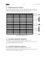
1
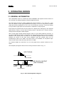
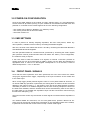
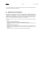
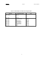
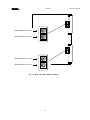
Technical
Information
Manual
Revision n. 0
25 January 2001
MOD. V534
8 CHANNEL
FLASH ADC
WITH MEMORY
CAEN will repair or replace any product within the guarantee period if the Guarantor
declares that the product is defective due to workmanship or materials and has not been
caused by mishandling, negligence on behalf of the User, accident or any abnormal
conditions or operations.
CAEN declines all responsibility for damages or
injuries caused by an improper use of the Modules
due to negligence on behalf of the User. It is strongly
recommended to read thoroughly the CAEN User's
Manual before any kind of operation.
CAEN reserves the right to change partially or entirely the contents of this Manual at any time and without
giving any notice.
25/01/96
V534 User's Manual
TABLE OF CONTENTS
TABLE OF CONTENTS ...................................................................................................... i
LIST OF FIGURES............................................................................................................. i
LIST OF TABLES ............................................................................................................... ii
1. DESCRIPTION............................................................................................................. 1
1.1. FUNCTIONAL DESCRIPTION ....................................................................... 1
2. SPECIFICATIONS........................................................................................................ 3
2.1. EXTERNAL COMPONENTS .......................................................................... 3
2.2. INTERNAL COMPONENTS ........................................................................... 3
2.3. POWER REQUIREMENTS ............................................................................ 3
2.4. CHARACTERISTICS OF THE SIGNALS ........................................................ 4
2.5. GENERAL .................................................................................................... 4
3. OPERATING MODES................................................................................................... 7
3.1. GENERAL INFORMATION............................................................................ 7
3.2. POWER-ON CONFIGURATION..................................................................... 8
3.3. VME SETTINGS............................................................................................ 8
3.4. FRONT PANEL SIGNALS.............................................................................. 8
3.5. MEMORY BLOCKS READOUT...................................................................... 9
4. VME INTERFACE ........................................................................................................ 10
4.1. ADDRESSING CAPABILITY .......................................................................... 10
4.2. MEMORY BLOCKS CONTENT...................................................................... 13
4.3. SET MODE "REGISTER" REGISTER............................................................. 13
4.4. SET MODE "MEMORY" REGISTER............................................................... 13
4.5. RESET REGISTER ....................................................................................... 14
4.6. STOP REGISTER ......................................................................................... 14
4.7. RELEASE BLOCK A REGISTER.................................................................... 14
4.8. RELEASE BLOCK B REGISTER.................................................................... 14
4.9. LATCH AND STATUS REGISTERS ............................................................... 14
4.10. DAC SET REGISTER.................................................................................... 16
4.11. EVENT COUNTER REGISTER...................................................................... 16
LIST OF FIGURES
Fig. 1.1: V534 Block Diagram .............................................................................................. 2
Fig. 2.1: Mod. V534 Front Panel .......................................................................................... 5
Fig. 2.2: Mod. V534 Components Locations ......................................................................... 6
Fig. 3.1: Mod. V534 Digitization Diagram.............................................................................. 7
Fig. 4.1: Mod. V534 Base Address Setting ........................................................................... 12
Fig. 4.2: Memory Blocks Content ......................................................................................... 13
Fig. 4.3: Latch and Status Registers .................................................................................... 15
Fig. 4.4: Complete Address of the Memory Locations ........................................................... 15
Fig. 4.5: DAC Set Register .................................................................................................. 16
Fig. 4.6: Event Counter Register.......................................................................................... 16
i
25/01/96
V534 User's Manual
LIST OF TABLES
Table 4.1: Address Map for the Mod. V534 in Memory Mode................................................. 10
Table 4.2: Address Map for the Mod. V534 in Register Mode ................................................ 11
ii
25/01/96
V534 User's Manual
1. DESCRIPTION
1.1.FUNCTIONAL DESCRIPTION
The CAEN Model V534 is a FLASH ADC WITH MEMORY housed in a 1-unit wide VME
module that implements the functions of an 8-channel 8 bit voltage sampling Analog-toDigital Converter (a functional block diagram is shown in Fig. 1.1).
The ADC block converts a differential analog voltage that must lie between +1.5 V and
+3.3 V. The User can sample an input signal (IN) varying in a 512 mV range with a pedestal
value that can be set between 0 V and +2.5 V via an internal 12 bit DAC. A Common Analog
Input provides a signal path to all 8 channels for calibration or test purposes.
Each channel is provided with 2 memory blocks of 4 Kbytes each, belonging to 2 separate
global blocks, namely A and B. Each memory block is structured as a circular memory,
holding the last 4 Kbytes of data samples.
It is possible to operate the module (selection via an internal dip switch) either by an internal
CLOCK, at a frequency of 20 MHz, or by an external one through the LEMO 00 connector
"CLK" housed on the front panel. Upon receipt of a CLOCK pulse, each input signal is
converted to an 8-bit word and stored on the first memory block available.
When a stop trigger (STOP) external signal is sent to a front panel LEMO 00 connector, or
an internal VME stop operation is performed, the working block is freezed, the first accessed
address in the memory block is stored on an Address Register and the next incoming
samples are stored on the other block available, while the freezed block can be
simultaneously read out via VME. If the other block is not available, the acquisition stops
until the User doesn't read and empty this block via VME.
Two external LEMO 00 connectors, one for each global block, provide a Block Full TTL
signal.
A front panel LED (DTACK) lights up each time the module generates the VME signal
DTACK.
The module works in A24/A32 mode; the recognized Address Modifier codes are:
AM=
AM=
AM=
AM=
%3D
%39
%0D
%09
standard supervisor data access;
standard user data access;
extended supervisor data access;
extended user data access.
The module's Base Address is fixed by 4 internal rotary switches housed on two piggy-back
boards plugged into the main printed circuit board. The Base Address can be selected in the
range:
%00 0000
--> %FF 0000
%0000 0000 --> %FFFF 0000
A24 mode;
A32 mode.
The Data Transfer occurs in D16/D32 mode.
1
25/01/96
V534 User's Manual
INPUT SECTION: ONE CHANNEL
x8
INPUT SECTION: ONE CHANNEL
COMMON IN
Σ
IN
MEMORY
ADC
VME
INTERFACE
+
IN
-
Σ
ADC
MEMORY
DAC
VME
BUS
ADDRESS
GENERATOR
A FULL
B FULL
CONTROL
LOGIC
STOP
Fig. 1.1: V534 Block Diagram
2
EVENT
COUNTER
25/01/96
V534 User's Manual
2. SPECIFICATIONS
2.1.EXTERNAL COMPONENTS
CONNECTORS
- No. 1, "IN 0÷7", input connector, Header 3M 3408-5202 type, 8+8 pins. Connector for the
INPUT differential analog signals.
- No. 1, "COMMON IN", LEMO 00 type. Connector for the COMMON IN analog signal.
- No. 2, "CLK", input bridged connectors, LEMO 00 type. Connectors for the external
CLOCK signal.
- No. 2, "STOP", input bridged connectors, LEMO 00 type. Connectors for the external
STOP signal.
- No. 2, "A F, B F", LEMO 00 type. Connectors for the output Block A Full and Block B Full
signals.
DISPLAYS
- No. 1, "DTACK", green LED, VME Selected; it lights up during a VME access.
2.2.INTERNAL COMPONENTS
SWITCHES
- No. 4, rotary switches for the module VME BASE address selection.
2.3. POWER REQUIREMENTS
+ 12 V
− 12 V
+5V
65 mA
500 mA
1.7 A
3
25/01/96
2.4. CHARACTERISTICS OF THE SIGNALS
INPUTS:
- IN 0÷7:
Differential analog signals, 110 Ω impedance;
Coupling: DC.
- COMMON IN:
Analog Level, high impedance;
Input Range: 0 V to +1.6 V.
- CLOCK:
TTL level, high impedance.
Maximum frequency: 20 MHz.
Duty cycle: 50%.
- STOP:
NIM/TTL level, high impedance.
Minimum width: 10 ns.
OUTPUTS:
- A F, B F:
Std. TTL level on 50 Ω impedance.
2.5. GENERAL
Resolution:
8 bits.
Input Sensitivity:
2 mV/count on the differential analog input (IN 0..7);
7 mV/count on the COMMON input;
7 mV/count on the internal 12 bit DAC value.
Total internal memory:
64 Kbytes.
Internal CLOCK frequency: 20 MHz.
Integral Non-linearity: ± 1 LSB.
Differential Non-linearity: ± 0.5 LSB.
4
V534 User's Manual
25/01/96
V534 User's Manual
Mod. V560E
VME selected LED
Mod. V534
DTACK
S
T
O
P
STOP input
C
L
K
External CLOCK
AF
BF
BLOCK FULL
Signals
COMMON
IN
Common Input
- +
0
Inputs 0..7
7
IN
SCALER
8 CH
MEMORY
FADC
Fig. 2.1: Mod. V534 Front Panel
5
25/01/96
V534 User's Manual
VME P1 connector
Rotary switches
for Base address selection
CLOCK Selector
Dip switch:
INTERNAL
(Visible Dot)
EXTERNAL
(No Dot)
Rotary switches
for Base address selection
VME P2 connector
Component side of the board
Fig. 2.2: Mod. V534 Components Locations
6
25/01/96
V534 User's Manual
3. OPERATING MODES
3.1.GENERAL INFORMATION
The CAEN Model V534 is a FLASH ADC WITH MEMORY that implements the functions of
an 8-channel 8 bit voltage sampling Analog-to-Digital Converter.
The ADC block converts an analog voltage that must lie between +1.5 V and +3.3 V. The
User can sample an input signal (ANALOG IN) varying in a 512 mV range with a pedestal
value that can be set between 0 V and +2.5 V via an internal 12 bit DAC. A Common Analog
Input provides a signal path to all 8 channels for calibration or test purposes.
Each channel is provided with 2 memory blocks of 4 Kbytes each, belonging to two separate
global blocks, namely A and B. Each memory block is structured as a circular memory,
holding the last 4 Kbytes of data samples.
When a stop trigger (STOP) external signal is sent to a front panel LEMO 00 connector, or
an internal VME stop operation is performed, the working block is freezed, the first accessed
address in the memory block is stored on an Address Register and the next incoming
samples are stored on the other block available, while the freezed block can be
simultaneously read out via VME. If the other block is not available, the acquisition stops
until the User doesn't read and empty this block via VME.
Two external LEMO 00 connectors, one for each global block, provide a Block Full TTL
signal.
The sampled input signal is stored in the memory blocks as shown in Fig. 3.1.
INPUT SIGNAL
STOP TRIGGER
MEMORY BLOCK CONTENT
(ONE CHANNEL)
DATUM 0
DATUM 4095
LATCH ADDRESS
Fig. 3.1: Mod. V534 Digitization Diagram
7
25/01/96
V534 User's Manual
3.2.POWER-ON CONFIGURATION
Once set the VME Address of the module via rotary switches (see § 4.1) and selected the
CLOCK mode via dip-switch (see Fig. 2.2) the module can be inserted in the VME crate and
powered-on. At Power-On the module appears to be in the following configuration:
- The module can be either in "Register" or in "Memory" mode;
- The memory blocks are full and not writable;
- The Event Counter is 0.
3.3.VME SETTINGS
In order to perform an ordinary sampling acquisition, the User must perform, before any
other operation, a RESET of the module by accessing the RESET Register.
After this, the User must release the blocks A and B by accessing the RELEASE BLOCK A
and RELEASE BLOCK B Registers.
The next operation MUST be a software STOP, performed by accessing the STOP register
(this operation must be performed also when both blocks are "IDLE"). In this configuration,
the module is ready to acquire.
If the User wants to shift the baseline of its signals, an internal 12 bit DAC provides an
analog value that can be programmed via VME by writing into the DAC SET Register the
appropriate value. A value of 0 in this Register corresponds to 0 V on the DAC; a value of
4096 corresponds to + 2.5 V on the DAC.
3.4. FRONT PANEL SIGNALS
Once that the above operations have been performed, the User must connect the cables
carrying the signals and the trigger, respectively to the Input connectors of the module and
to the STOP input.
When a stop trigger (STOP) external signal is sent to a front panel LEMO 00 connector, or
an internal VME stop operation is performed, the working block is freezed, the first accessed
address in the memory block (i. e., the location of the first of the 4096 samples containing
valid data) is stored on an Address Register and the next incoming samples are stored on
the other block available, while the freezed block can be simultaneously read out via VME. If
the other block is not available the acquisition stops until the User doesn't read and empty
this block via VME (see § 3.5).
The Event Counter counts only the number of STOP signals occurred while the acquisition is
active.
Two external LEMO 00 connectors, one for each global block, provide a Block Full TTL
signal, that can be used to provide some information on the acquisition status of the module,
in particular the fact that the module cannot accept a further STOP signal.
8
25/01/96
V534 User's Manual
Two external LEMO 00 input bridged connectors accept an external CLOCK signal (Clock
mode selection via dip switch, see Fig. 2.2).
3.5. MEMORY BLOCKS READOUT
The memory of the module is overlapped to the Registers: in Register Mode all the
Addresses up to Base Address + %0C are accessed, while in Memory Mode all the
Addresses up to Base Address + %FFFF are accessed. The switching from Register Mode
to Memory Mode is performed with a write access to appropriate registers (Mode Register,
Base Addr. + %04, and Mode Memory, Base Addr. + %06, registers).
In order to readout the content of a Memory block, the User should perform the following
operations:
- Switch the module to "Register" mode;
- Read the Latch Address in the Latch and Status Register of that block;
- Calculate the complete 32 bit address of the first latched location in the Memory block
(see § 4.9);
- Switch the module to Memory Mode,
- Start the readout of the Memory block from the first location to the end of the block, and
subsequently, from the beginning of the block to the position corresponding to Latch
Address - 4;
- Release the block with an access to the relevant Release Block Register.
9
25/01/96
V534 User's Manual
4. VME INTERFACE
4.1. ADDRESSING CAPABILITY
The V534 module works in A24/A32, D16/D32 mode. This means that the module address
must be specified in a field of 24 or 32 bits. The Address Modifiers codes recognized by the
module are:
AM=%3D:
AM=%39:
AM=%0D:
AM=%09:
standard supervisor data access
standard user data access
extended supervisor data access
extended user data access
The module's Base Address is fixed by 4 internal rotary switches housed on two piggy-back
boards plugged into the main printed circuit board (see Fig. 4.0).
The Base Address can be selected in the range:
% 00 0000 <-> % FF 0000
% 0000 0000 <--> % FFFF 0000
A24 mode
A32 mode
The Base Address reserves in this way a page of 64 Kbytes for the module.
The Address Map of the module is overlapped: in Register Mode the addresses up to Base
Add. + %0C are accessed, while in Memory mode all the addresses up to Base Add. +
%FFFF are accessed (8 Kbytes per channel, for a total of 64 Kbytes of memory). The
switching from Register Mode to Memory Mode is performed with a write access to
appropriate registers (Mode Register, Base Addr. + %04, and Mode Memory, Base Addr. +
%06, registers).
The Address Map in Memory Mode is shown in Table 4.1; the Address Map in Register
Mode is shown in Table 4.2.
Table 4.1: Address Map for the Mod. V534 in Memory Mode
ADDRESS
Base + %0000
Base + %4000
Base + %8000
Base + %C000
REGISTER/CONTENT
Block A Low (Ch. 0÷3)
Block A High (Ch. 4÷7)
Block B Low (Ch. 0÷3)
Block B High (Ch. 4÷7)
10
TYPE
read only
read only
read only
read only
25/01/96
V534 User's Manual
Table 4.2: Address Map for the Mod. V534 in Register Mode
ADDRESS
REGISTER/CONTENT
Base + %FFFE
.
.
Base + %0E
Reserved
.
.
Reserved
Base + %0C
Base + %0C
Base + %0A
Base + %0A
Base + %08
Base + %08
Base + %06
Base + %04
Base + %02
Base + %00
Read Event Counter
Stop
Release Block B
Latch B and Status
Release Block A
Latch A and Status
Set Mode Memory
Set Mode Register
Set DAC
Reset
11
TYPE
read only
write only
write only
read/write
write only
read only
write only
write only
write only
write only
25/01/96
Base address bit <23..20>
Base address bit <19..16>
Base address bit <31..28>
Base address bit <27..24>
Fig. 4.1: Mod. V534 Base Address Setting
12
V534 User's Manual
25/01/96
V534 User's Manual
4.2. MEMORY BLOCKS CONTENT
The 64 Kbytes of reserved memory contain the sampling data of both blocks for each
channel. The readout of the memory can be done only when the module is in "Memory"
mode. The content of each register/block is shown in the following Figure.
Ch. 3 Datum 0
Ch. 2 Datum 0
Ch. 1 Datum 0
Ch. 0 Datum 0
ADDRESS
Base + %0000
Ch. 3 Datum 1
Ch. 2 Datum 1
Ch. 1 Datum 1
Ch. 0 Datum 1
Base + %0004
...
...
...
...
Ch. 3 Datum 4095
Ch. 2 Datum 4095
Ch. 1 Datum 4095
Ch. 0 Datum 4095
Base + %3FFC
Ch. 7 Datum 0
Ch. 6 Datum 0
Ch. 5 Datum 0
Ch. 4 Datum 0
Base + %4000
Ch. 7 Datum 1
Ch. 6 Datum 1
Ch. 5 Datum 1
Ch. 4 Datum 1
Base + %4004
...
...
...
...
Ch. 7 Datum 4095
Ch. 6 Datum 4095
Ch. 5 Datum 4095
Ch. 4 Datum 4095
Base + %7FFC
Ch. 3 Datum 0
Ch. 2 Datum 0
Ch. 1 Datum 0
Ch. 0 Datum 0
Base + %8000
Ch. 3 Datum 1
Ch. 2 Datum 1
Ch. 1 Datum 1
Ch. 0 Datum 1
Base + %8004
...
...
...
...
Ch. 3 Datum 4095
Ch. 2 Datum 4095
Ch. 1 Datum 4095
Ch. 0 Datum 4095
Base + %BFFC
Ch. 7 Datum 0
Ch. 6 Datum 0
Ch. 5 Datum 0
Ch. 4 Datum 0
Base + %C000
Ch. 7 Datum 1
Ch. 6 Datum 1
Ch. 5 Datum 1
Ch. 4 Datum 1
Base + %C004
...
...
...
...
Ch. 7 Datum 4095
Ch. 6 Datum 4095
Ch. 5 Datum 4095
Ch. 4 Datum 4095
31 30 29 28 27 26 25 24 23 22 21 20 19 18 17 16 15 14 13 12 11 10 9 8
7 6 5
4 3
2 1 0
...
...
...
...
Base + %FFFC
Fig. 4.2: Memory Blocks Content
4.3. SET MODE "REGISTER" REGISTER
(Base Address + %04, write only, module in "Memory" or "Register" mode)
The Set Mode "Register" Register is located at the Address Base + %04. A write access to
this register switches the module in Register Mode.
4.4. SET MODE "MEMORY" REGISTER
(Base Address + %06, write only, module in "Memory" or "Register" mode)
The Set Mode "Memory" Register is located at the Address Base + %06. A write access to
this register switches the module in Memory Mode.
13
25/01/96
V534 User's Manual
4.5. RESET REGISTER
(Base Address + %00, write only, module in "Memory" or "Register" mode)
The Reset Register is located at the Address Base + %00. Any write access to this register
resets the module, i.e., the acquisition becomes "IDLE". The module can be either in
"Register" or in "Memory" mode.
4.6. STOP REGISTER
(Base Address + %0C, write only, module in "Memory" or "Register" mode)
The Stop Register is located at the Address Base + %0C. Any write access to this register
generates an internal STOP of the module. This operation must be performed via software
when both blocks are "IDLE" (see § 3.3). The module can be either in "Register" or in
"Memory" mode.
4.7. RELEASE BLOCK A REGISTER
(Base Address + %08, write only, module in "Memory" or "Register" mode)
The Release Block A Register is located at the Address Base + %08. Any write access to
this register releases the Block A of the module memory. The module can be either in
"Register" or in "Memory" mode.
4.8. RELEASE BLOCK B REGISTER
(Base Address + %0A, write only, module in "Memory" or "Register" mode)
The Release Block B Register is located at the Address Base + %0A. Any write access to
this register releases the Block B of the module memory. The module can be either in
"Register" or in "Memory" mode.
4.9. LATCH AND STATUS REGISTERS
(Base Address + %08, +%0A, read only, module in "Register" mode only)
The Latch and Status Registers consist of one 16 bit register per Memory Block: the address
Base + %08 contains the Latch Address of Block A in the 12 least significant bits; the
address Base + %0A contains the Latch Address of Block B in the 12 least significant bits;
the 4 most significant bits of both Registers are the Status bits:
bit 12 is the BUFFER A WORKING Bit (ACTIVE = 0, IDLE = 1);
bit 13 is the BUFFER A STATUS Bit (FULL=1, FREE=0);
bit 14 is the BUFFER B WORKING Bit (ACTIVE = 0, IDLE = 1);
bit 15 is the BUFFER B STATUS Bit (FULL=1, FREE=0).
14
25/01/96
15 14 13 12 11 10 9
BS
BW AS
AW
8
7
6
5
4
3
2
V534 User's Manual
1
0
LATCH ADDRESS A/B
LATCH ADDRESS
BUFFER A WORKING
BUFFER A STATUS
BUFFER B WORKING
BUFFER B STATUS
Fig. 4.3: Latch and Status Registers
In order to obtain the complete address of the first latched location in the memory blocks, the
User should shift by two the 12 bits of the Latch Address and complete the lower part of the
word with two bits to select the memory block portion (Block A Low, Block A High, Block B
low, Block B High). The 8 (16) most significant bits are the Base Address MSBs (see Fig.
4.4).
23 22 21 20 19 18 17 16 15 14 13 12 11 10 9 8 7 6 5 4 3 2 1 0
A24 mode
Base Add. (8 MSB) 0 0
Latch A Address
0 0
Block A Low
Base Add. (8 MSB) 0 1
Latch A Address
0 0
Block A High
Base Add. (8 MSB) 1 0
Base Add. (8 MSB) 1 1
Latch B Address
0 0
Block B Low
Latch B Address
0 0
Block B High
31 30 29 28 27 26 25 24 23 22 21 20 19 18 17 16 15 14 13 12 11 10 9 8 7 6 5 4 3 2 1 0
A32 mode
Base Address (16 MSB)
0 0
Latch A Address
0 0
Block A Low
Base Address (16 MSB)
0 1
Latch A Address
0 0
Block A High
Base Address (16 MSB)
1 0
Latch B Address
0 0
Block B Low
Base Address (16 MSB)
1 1
Latch B Address
0 0
Block B High
Fig. 4.4: Complete Address of the Memory Locations
15
25/01/96
V534 User's Manual
4.10. DAC SET REGISTER
(Base Address + %02, write only, module in "Memory" or "Register" mode)
The DAC Set Register is located at the Address Base + %02. This register contains in D0÷
D11 the value to be sent to the DAC. The module can be either in "Memory" or "Register"
mode.
15 14 13 12 11 10 9
8
7
6
5
4
3
2
1
0
DAC SET VALUE
12 bit DAC Setting
Not Used
Fig. 4.5: DAC Set Register
4.11. EVENT COUNTER REGISTER
(Base Address + %0C, read only)
The Event Counter Register is located at the Address Base + %0C. This register contains in
D0÷D17 the Event Counter value. This Register is incremented upon receipt of a valid STOP
signal, i. e. when the module acquisition is "ACTIVE".
15 14 13 12 11 10 9
8
7
6
5
4
3
2
1
0
EVENT COUNTER
Event Counter value
Not Used
Fig. 4.6: Event Counter Register
16