1
25/01/96
V462 User's Manual
TABLE OF CONTENTS
TABLE OF CONTENTS ..........................................................................................................i
LIST OF FIGURES .................................................................................................................i
LIST OF TABLES....................................................................................................................i
1. DESCRIPTION .................................................................................................................1
1.1. FUNCTIONAL DESCRIPTION ..........................................................................1
2. SPECIFICATIONS............................................................................................................3
2.1. EXTERNAL COMPONENTS.............................................................................3
2.2. INTERNAL COMPONENTS ..............................................................................4
2.3. POWER REQUIREMENTS ...............................................................................4
2.4. CHARACTERISTICS OF THE SIGNALS ..........................................................4
3. OPERATING MODES.......................................................................................................6
3.1. GENERAL INFORMATION ...............................................................................6
3.2. POWER-UP CONFIGURATION........................................................................6
3.3. FRONT PANEL SETTINGS ..............................................................................6
3.4. VME SETTINGS ...............................................................................................7
3.5. FRONT PANEL SIGNALS.................................................................................8
4. VME INTERFACE.............................................................................................................9
4.1. ADDRESSING CAPABILITY .............................................................................9
4.2. MODULE IDENTIFIER WORDS........................................................................11
4.3. GENERATORS REGISTERS............................................................................11
4.4. CONTROL AND STATUS REGISTER ..............................................................11
APPENDIX A: ELECTRICAL DIAGRAMS ...............................................................................A.1
APPENDIX B: COMPONENT LIST AND LOCATIONS............................................................B.1
LIST OF FIGURES
Fig. 1.1: V462 Block Diagram ..................................................................................................2
Fig. 2.1: Mod. V 462 Front Panel.............................................................................................5
Fig. 2.2: Mod. V462 components locations ..............................................................................6
Fig. 3.1: Gate Generator Width Registers................................................................................8
Fig. 3.2: Control and Status Register.......................................................................................9
Fig. 4.1: Mod. V462 Base address setting ...............................................................................11
Fig. 4.2: Module Identifier words..............................................................................................12
LIST OF TABLES
Table 4.1: Address Map for the Mod. V462..............................................................................10
i
25/01/96
V462 User's Manual
1. DESCRIPTION
1.1. FUNCTIONAL DESCRIPTION
The CAEN Model V462 is a DUAL GATE GENERATOR housed in a 1-unit wide VME
module (a functional block diagram is shown in Fig. 1.1).
Each module consists of two Gate Generators, one per channel, independently
programmable between 100 ns and 9.9999999 s. These generate three standard NIM
signals: a Gate, a Begin Marker, of fixed 100 ns width, simultaneous to the beginning of the
Gate, and an End Marker, of fixed 100 ns width, simultaneous to the end of the Gate.
The module is based on the use of Programmable Gate Arrays containing almost all the
logic of each generator's operations. There are two working registers per channel, one for
Local Mode, the other for VME Mode.
In Local Mode, the content of the Local Register is transferred to eight 4-bit multiplexers,
that allow displaying of the gate width , and is presented to some bit-to-bit comparators.
The module contains eight 4-bit BCD counters that are positioned to zero if the gate is not
triggered. When the Start signal takes place, the counters start counting at 10 MHz
frequency and the output of these counters is presented to the other input of the
comparators.
When the 32 bit word of the counters reaches the one of the selected register, the counting
stops and the gate signal ends. A new cycle is possible right after the End of Gate Marker
signal.
The Local Mode is characterized by the display of the content of the Local Register, which
becomes the register to compare with the counters. Moreover, in Local Mode, the User can
modify the content of the register via 4 push buttons and set a different width of the Gate. A
digit (unit) that is selected via the DIG SEL +/- push buttons starts blinking, and the value of
the digit can be incremented/decremented with the FIG SEL +/- push buttons.
The VME Mode is characterized by the display of the content of the VME Register, which
becomes the register to compare with the counters. The gate triggering and width are
programmable via VME. The selection switches and push-buttons for the width setting
become totally ineffective on the selected register.
Whichever operating mode is selected, the Gate can always be triggered by the NIM signal
or the push-button "START" for each channel. When the Gate signal is present, and for all
the Gate duration, all the START signals are ignored ("Non-Updating" operation).
The Model V462 is an A24 D16 VME slave; its Base address is fixed by 4 internal rotary
switches. A front panel LED (DTACK) lights up each time the module generates the VME
signal DTACK.
(This module is a CEA-IRF SACLAY design)
1
25/01/96
V462 User's Manual
DATA
TRANSFER
GENERATOR
COMMANDS
VME REGISTER
COMMON
COMMANDS
GENERATOR
NIM INPUTS
VME
VME
INTERFACE
BUS
NIM OUTPUTS
LOCAL REGISTER
DISPLAY
BLOCK
IDENTIFIER
Fig. 1.1: V462 Block Diagram
2
25/01/96
V462 User's Manual
2. SPECIFICATIONS
2.1. EXTERNAL COMPONENTS
CONNECTORS
- No. 2, "START", LEMO 00 type, 50 Ω impedance. Connectors for the START signal for
each channel.
- No. 4, "GATE", LEMO 00 type, 50 Ω impedance. Connectors for the output GATE signal
for each channel: a fan-out of 2 is provided for each channel.
- No. 4, "B. M.", LEMO 00 type, 50 Ω impedance. Connectors for the output Begin of Gate
Marker signal for each channel: a fan-out of 2 is provided for each channel.
- No. 4, "E. M.", LEMO 00 type, 50 Ω impedance. Connectors for the output End of Gate
Marker signal for each channel: a fan-out of 2 is provided for each channel.
DISPLAYS
- No. 1, "DTACK", green LED, VME Selected; it lights up during a VME access.
- No. 1, "BERR", red LED, VME Selected; it lights up if a Bus Error occurs.
- No. 4, red 7 segment 4 figures LEDs, 2 for each channel, to indicate the gate width
between 0.0000000 and 9.9999999 sec.
- No. 2, "LOC", red LEDs, 1 for each channel. Light up if the module is working in Local
Mode.
- No. 2, "OUT", green LEDs, 1 for each channel. Light up if the Gate signal is present.
SWITCHES
- No. 1, "CH0 - CH1", Lever switch selector, to modify Channel 0 or Channel 1 gate width.
- No. 2, "LOC", Manual Push-Buttons for the selection of Local or VME gate width setting.
- No. 2, "START", Manual Push-Buttons for the gate trigger .
- No. 2, "DIG SEL +, -", Manual Push-Buttons to increment/decrement the digit position in
the gate width display (i. e. the unit to increment/decrement with the FIG SEL button).
- No. 2, "FIG SEL +, -", Manual Push-Buttons to increment/decrement the value of the
selected digit of the gate width display.
3
25/01/96
V462 User's Manual
2.2. INTERNAL COMPONENTS
SWITCHES
- No. 4, rotary switches for the module VME BASE address selection.
2.3. POWER REQUIREMENTS
+ 12 V
− 12 V
+5V
30 mA
500 mA
1A
2.4. CHARACTERISTICS OF THE SIGNALS
INPUTS:
- START:
Std. NIM level, 50 Ω impedance;
Minimum pulse width: 20 ns.
OUTPUTS:
- GATE:
Std. NIM level on 50 Ω impedance;
Min. width: 100 ns;
START to GATE delay: 140 ± 10 ns;
Rise Time: < 1.5 ns;
Fall Time: < 2.5 ns.
- BEGIN MARKER:
Std. NIM level on 50 Ω impedance;
Width: 100 ns;
START to BEGIN MARKER delay: 140 ± 10 ns;
Leading Edge B. MARKER to Leading Edge GATE delay: 3 ns.
- END MARKER:
Std. NIM level on 50 Ω impedance;
Width: 100 ns;
Trailing Edge GATE to Leading Edge E. MARKER delay: 3 ns.
4
25/01/96
V462 User's Manual
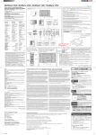
Mod. V560E
Mod. V462
BERR
DTACK
BUS ERROR LED
VME SELECTED LED
CH0
s |
DISPLAYS CH0
ms
1 |100' 10 ' 1
µ s
| ns
100 ' 10 ' 1 |100'
PUSH BUTTON FOR
LOCAL MODE SELECTION
LOC
START
PUSH BUTTON START
EXT. SIGNAL START
OUT
G
A
T
E
GATE OUT
B.
M.
BEGIN MARKER
E.
M.
END MARKER
FIG SEL
−
CHANNEL SELECTION
FIGURE SEL. PUSH BUTTON
+
CH1
CH0
−
+
DIGIT SEL. PUSH BUTTON
DIG SEL
CH1
s |
ms
1 |100' 10 ' 1
µ s
| ns
100 ' 10 ' 1 |100'
LOC
START
OUT
G
A
T
E
B.
M.
E.
M.
16 CH
SCALER
DUAL GATE
GENERATOR
Fig. 2.1: Mod. V 462 Front Panel
5
25/01/96
V462 User's Manual
VME P1 connector
Rotary switches
for Base address selection
Component side of the board
Fig. 2.2: Mod. V462 components locations
6
25/01/96
V462 User's Manual
3. OPERATING MODES
3.1. GENERAL INFORMATION
To understand the operating modes of the module, it's important to distinguish between the
VME operating mode and the totally independent manual operating mode via the front
panel.
For example, two Users can operate on the module, knowing that the front panel User has
always priority to the one operating via VME. As the module contains two generators, the
front panel User can operate only on one of the two at a time, and in this case the other
generator is completely accessible by the VME bus.
The use of the Programmable Gate Arrays (PGAs) reduces to a minimum the need for
external logic. One single Gate Array takes charge of all the register commands logic, of the
Control and Status Register management and of the front panel commands. It controls
completely the other Gate Arrays.
3.2. POWER-UP CONFIGURATION
The use of the PGAs requires a period of initialization at power-up of duration not greater
than 1 sec, thus less than 200 msec shorter than the VME Sysreset signal. During this
phase, the PGA's inputs and outputs are not available and are in high impedance
configuration. For this reason, the module is completely inaccessible either via VME or via
front panel. If the VME bus sends some commands or data, the module is completely
transparent (no response) just as if it was disconnected from the VME bus.
This period corresponds to the loading of a particular program stored on some PROMs
placed on the board. This loading enables the configuration of the inputs/outputs of the
PGAs.
The PGAs are very sensitive to the quality of the supply voltage. In fact, in case of great
fluctuations of the voltage, or in case of brief power shortages, the PGAs may be erased in
part. Thus a special circuit has been inserted to reset to zero the PGAs each time the supply
voltage falls below 4.5 V.
3.3. FRONT PANEL SETTINGS
To set manually a certain gate width, one should select the desired channel with the front
panel switch and push the button Local on the selected channel to enter in Local Mode
(Local LED lights on). Note that at power-on the two channels are in VME Mode. At the first
time the module enters in Local Mode after power-on, the display will show a value of the
gate which is NOT reliable: the User must set the gate width on ALL the digits in the display,
and after this the Local Register will always keep the set value until the next power-off.
After a pression on the "Dig Sel −" push button, the point of the most significant digit
(seconds) in the display starts blinking, indicating that the value read out on the display is
7
25/01/96
V462 User's Manual
stored automatically in the Local Register. By pushing the "Fig Sel +" or the "Fig Sel −" push
buttons, the value of the current digit (with blinking point) can be incremented/decremented.
By pushing the "Dig Sel −" or the "Dig Sel +" push buttons, the blinking point goes down to
the lower digits or up to the higher digits in the display (except for a position in which the
point doesn't appear), carrying the value of the previous blinking digit to the current one.
This last feature enables the writing of big numbers without going through each single figure.
For example, if the User wants to write 1 sec, it is sufficient to set 1 in the most significant
(seconds) digit, to position on the hundreds of milliseconds digit and set 0, and "carry" the
value 0 to the other digits with the "Dig Sel −" button. The displayed value will then be
10000000.
A second pressing of the Loc button cancels the blinking point and restores the VME
Operating Mode.
3.4. VME SETTINGS
Via VME it is possible to read/write the content of the Generators registers (gate width).
These registers are composed of two 16 bit registers per channel: the address Base + %08
contains the 4 least significant digits of the gate width for channel 1; the address Base +
%06 contains the 4 most significant digits of the gate width for channel 1; the address Base
+ %04 contains the 4 least significant digits of the gate width for channel 0; the address
Base + %02 contains the 4 most significant digits of the gate width for channel 0.
The Write operation on the VME Generator register can be done at any time, also when the
channel is in Local mode, but when the channel is in Local the Read operation returns the
content of the Local register. Anyway, it is suggested NOT to access via VME the channel in
Local mode.
It is also suggested to perform the most significant value cycles and the least significant
value cycles in the correct order (most-least) to avoid errors in the VME Registers.
If the User wants to set a desired value of the gate width, e. g. 123 µsec for channel 0,
He/She has to write 0 in the address Base + %02 and 1230 in the address Base + %04.
BASE + %08
15 14 13 12 11 10 9 8 7 6 5 4 3 2 1 0
LEAST SIGNIFICANT DIGITS CHANNEL 1
BASE + %06
15 14 13 12 11 10 9 8 7 6 5 4 3 2 1 0
MOST SIGNIFICANT DIGITS CHANNEL 1
BASE + %04
15 14 13 12 11 10 9 8 7 6 5 4 3 2 1 0
LEAST SIGNIFICANT DIGITS CHANNEL 0
BASE + %02
15 14 13 12 11 10 9 8 7 6 5 4 3 2 1 0
MOST SIGNIFICANT DIGITS CHANNEL 0
Fig. 3.1: Gate Generator Width Registers
8
25/01/96
V462 User's Manual
The Control and Status Register is located at the Address Base + %00. This register
contains some information on the status of the module in the 5 most significant bits (active
high):
the bit in D15 is an error bit, and indicates that one of the two generators is either in local
mode or that its gate signal is present; the bits in D14 and D13 indicate that, respectively,
channel 1 or channel 0 are in VME or Local mode (bits low if in VME mode); the bits in D12
and D11 indicate that, respectively, the gate signal of channel 1 or channel 0 is present.
Every attempt to write into one of these 5 bits generates a Bus Error and a LED on the front
panel (BERR) lights on.
Only two bits of the Control and Status Register can be used in write mode to trigger via
VME the gate generators. The bits in D10 and D9 of the Address Base + %00 (active high)
trigger respectively the channel 1 and channel 0 generators. Any attempt to read these two
bits is ineffective. The bits in D8 through D0 are meaningless.
BASE + %00
D15
D14
D13
D12
D11
D10
D9
ERR
VME/
VME/
GATE
GATE
START
START
LOC 1
LOC 0
CH. 1
CH. 0
CH. 1
CH 0
D8
...
D0
...
Fig. 3.2: Control and Status Register
3.5. FRONT PANEL SIGNALS
To trigger externally the Gate Generators, two START inputs (one per channel) can be sent
to the module. These should be standard NIM signals of 20 ns minimum width, otherwise
the Gate could not be triggered. A gate is triggered by the leading edge of the NIM "START"
signal.
Whichever operating mode is selected, the Gate can always be triggered by the NIM signal
or the push-button "START" for each channel. When the Gate signal is present, and for all
the Gate duration, all the START signals are ignored ("Non-Updating" operation).
There are three output signals with a fan-out of two for each channel: the Gate, the Begin
Marker and the End Marker. The Begin Marker is simultaneous with the Gate signal, and its
width is 100 ns. The End Marker is simultaneous with the Gate ending, and also its width is
100 ns.
The delay between the trigger signal and the leading edge of the Gate or Begin Marker
signals is 140 ns ± 10 ns.
9
25/01/96
V462 User's Manual
4. VME INTERFACE
4.1. ADDRESSING CAPABILITY
The V462 module works in A24 D16 mode. This means that the module address must be
specified in a field of 24 bits. The Address Modifiers codes recognized by the module are:
AM=%3D:
AM=%39:
AM=%0D:
AM=%09:
standard supervisor data access
standard user data access
extended supervisor data access
extended user data access
The module's Base Address is fixed by 4 internal rotary switches housed on two piggy-back
boards plugged into the main printed circuit board (see Fig. 4.1).
The Base Address can be selected in the range:
% 00 0000 <-> % FF FF00
A24 mode
The Base Address reserves in this way a page of 256 bytes for the module. The Address
Map is shown in table 4.1.
Table 4.1: Address Map for the Mod. V462
ADDRESS
REGISTER/CONTENT
Base + %FE
Base + %FC
Base + %FA
Version & Series
Manufacturer & Module Type
Fixed code
Base + %F8
.
.
Base + %10
Not used
.
.
Not used
Base + %08
Base + %06
Base + %04
Base + %02
Base + %00
Base + %00
L. S. B. Generator CH. 1
M. S. B. Generator CH. 1
L. S. B. Generator CH. 0
M. S. B. Generator CH. 0
Generators status
Start Gate Generators
10
TYPE
read only
read only
read only
read/write
read/write
read/write
read/write
read only
write only
25/01/96
Base address bit <11..8>
Base address bit <15..12>
Base address bit <19..16>
Base address bit <23..20>
Fig. 4.1: Mod. V462 Base address setting
11
V462 User's Manual
25/01/96
V462 User's Manual
4.2. MODULE IDENTIFIER WORDS
(Base address + %FA ,+%FC, +%FE read only)
The Three words located at the highest address on the page are used to identify the module
as shown in figure 4.2:
15 14 13 12 11 10 9
V e r s i o n
7
M o d u l e ' s
Manufacturer number
% F A
8
F i x e d
6
5
s e r i a l
M o d u l e
c o d e
4
% F 5
3
2
1
0
n u m b e r
Base + % FE
Base + % FC
t y p e
F i x e d
Address
c o d e
Base + % FA
Fig. 4.2: Module Identifier words
At the address Base + % FA the two particular bytes allow the automatic localization of the
module.
For the Mod. V462 the word at address Base + % FC has the following configuration:
Manufacturer N°=
000010 b
Type of module =
0000001010 b
The word located at the address Base + %FE identifies the single module through the
module's serial number and any change in the hardware will be shown by the Version
number.
4.3. GENERATORS REGISTERS
(Base Address + %08, +%06, + %04, + %02, read/write)
The Generators Registers (gate width duration) are composed of two 16 bit registers per
channel: the address Base + %08 contains the 4 least significant digits of the gate width for
channel 1; the address Base + %06 contains the 4 most significant digits of the gate width
for channel 1; the address Base + %04 contains the 4 least significant digits of the gate
width for channel 0; the address Base + %02 contains the 4 most significant digits of the
gate width for channel 0.
BASE + %08
15 14 13 12 11 10 9 8 7 6 5 4 3 2 1 0
LEAST SIGNIFICANT DIGITS CHANNEL 1
BASE + %06
15 14 13 12 11 10 9 8 7 6 5 4 3 2 1 0
MOST SIGNIFICANT DIGITS CHANNEL 1
BASE + %04
15 14 13 12 11 10 9 8 7 6 5 4 3 2 1 0
LEAST SIGNIFICANT DIGITS CHANNEL 0
BASE + %02
15 14 13 12 11 10 9 8 7 6 5 4 3 2 1 0
MOST SIGNIFICANT DIGITS CHANNEL 0
Fig. 3.1: Gate Generator Width Registers
12
25/01/96
V462 User's Manual
4.4. CONTROL AND STATUS REGISTER
(Base Address + %00, read only bits D15-D11, write only bits D10-D9)
The Control and Status Register is located at the Address Base + %00. This register
contains some information on the status of the module in the 5 most significant bits (active
high):
the bit in D15 is an error bit, and indicates that one of the two generators is either in local
mode or that its gate is open; the bits in D14 and D13 indicate that, respectively, channel 1
or channel 0 are in VME or Local mode (bits high if in VME mode); the bits in D12 and D11
indicate that, respectively, the gate of channel 1 or channel 0 is open. Every attempt to write
into one of these 5 bits generates a Bus Error and a LED on the front panel (BERR) lights
on.
Only two bits of the Control and Status Register can be used in write mode to trigger via
VME the gate generators. The bits in D10 and D9 of the Address Base + %00 (active high)
trigger respectively the channel 1 and channel 0 generators. Any attempt to read these two
bits is ineffective. The bits in D8 through D0 are meaningless.
BASE + %00
D15
D14
D13
D12
D11
D10
D9
ERR
VME/
VME/
GATE
GATE
START
START
LOC 1
LOC 0
CH. 1
CH. 0
CH. 1
CH 0
Fig. 3.2: Control and Status Register.
13
D8
...
...
D0
25/01/96
APPENDIX A: ELECTRICAL DIAGRAMS
A.1
V462 User's Manual
25/01/96
V462 User's Manual
APPENDIX B: COMPONENT LIST AND LOCATIONS
B.1