1
Technical
Information
Manual
Revision n. 0
21 April 1999
MOD. V 265
8 CHANNEL
CHARGE INTEGRATING
ADC
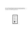
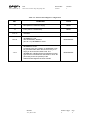
N.B.: For Mod. V265E, the following picture shows the polarities of
the GATE, CLEAR and BUSY signals on the couple of pins placed in
replacement of the LEMO 00 type connectors.
GATE
- +
CLR
- +
BUSY
- +
TEST
Document type:
User's Manual (MUT)
Title:
Mod. V265 8 channel charge integrating ADC
Revision date:
20/04/99
Revision:
0
TABLE OF CONTENTS
1.
1.1.
2.
DESCRIPTION .............................................................................................................................................3
FUNCTIONAL DESCRIPTION ......................................................................................................................3
SPECIFICATIONS .......................................................................................................................................6
2.1.
PACKAGING ..............................................................................................................................................6
2.2.
EXTERNAL COMPONENTS .........................................................................................................................6
2.3.
INTERNAL COMPONENTS ..........................................................................................................................6
2.4.
CHARACTERISTICS OF THE SIGNALS ..........................................................................................................7
2.5.
PERFORMANCES AND TEST RESULTS.........................................................................................................7
2.6.
POWER REQUIREMENTS ............................................................................................................................8
2.7.
INTEGRAL NON LINEARITY TEST PROCEDURE PERFORMED BY CAEN.......................................................9
3.
OPERATING MODE .................................................................................................................................10
3.1.
OPERATIONS TO BE PERFORMED .............................................................................................................10
3.2.
SOFTWARE PROGRAMS EXAMPLE ...........................................................................................................13
4.
CALIBRATION OPERATIONS ...............................................................................................................14
4.1.
NECESSARY INSTRUMENTS .....................................................................................................................14
4.2.
OPERATIONS TO BE PERFORMED .............................................................................................................14
5.
TEST LOGIC ..............................................................................................................................................16
Filename:
V265_REV0.DOC
Number of pages:
16
Page:
1
Document type:
User's Manual (MUT)
Title:
Mod. V265 8 channel charge integrating ADC
Revision date:
20/04/99
Revision:
0
LIST OF FIGURES
FIG. 1.1 – FUNCTIONAL BLOCK DIAGRAM OF THE MODULE...................................................................................4
FIG. 1.2 – MOD. V265 FRONT PANEL ....................................................................................................................5
FIG. 3.1 – ROTARY SWITCH AND JUMPER POSITION .............................................................................................10
FIG. 4.1 – INTERNAL TRIMMERS ..........................................................................................................................14
FIG. 4.2 – TIMING DIAGRAM ................................................................................................................................15
FIG. 5.1 – INTERNAL JUMPER J3 POSITION ...........................................................................................................16
LIST OF TABLES
TABLE 3.1 –INTERNAL ADDRESS SPECIFICATIONS ..................................................................................................11
TABLE 3.2 –STATUS/CONTROL REGISTER CONFIGURATION ....................................................................................12
Filename:
V265_REV0.DOC
Number of pages:
16
Page:
2
Document type:
User's Manual (MUT)
Title:
Mod. V265 8 channel charge integrating ADC
Revision date:
20/04/99
Revision:
0
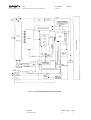
1. Description
1.1.
Functional Description
The Model V 265 8 CHANNEL CHARGE INTEGRATING ADC is an A24-D16 single width VME
Slave module provided with eight independent channels capable of converting the charge
associated with an input signal to a 16-bit word.
For each channel, the input charge is converted to a voltage level by a Charge to Voltage
Converter (CVC). The conversion process begins whenever a GATE input signal (NIM level)
becomes TRUE, and it stops when the GATE signal becomes FALSE.
As soon as the GATE becomes FALSE, each CVC output voltage is sequentially transformed to
a 16-bit word by two parallel 12-bit Analog to Digital Converters (ADC), and at the same time a
BUSY output signal is available at the corresponding front panel connector. During the time
interval in which the BUSY signal is active no GATE signal is accepted.
Each 16-bit word (containing the analog-to-digital conversion value, a channel identifier and an
ADC RANGE identifier) is stored into a FIFO memory (Data Register readable via VME) capable
of storing up to 16 events (i.e.:16*8*2 16-bit words). The current state (READY or FULL) of the
FIFO memory is signalled by two dedicated front panel LEDs ("RDY" and "FULL") and can be
known by reading the Status/Control Register via VME.
At the end of the analog-to-digital conversion of the last input signal, the BUSY signal is
automatically deactivated and the module's CVCs are cleared: in this way further inputs can be
converted.
The module (CVCs, internal registers and FIFO memory) can be cleared via VME or by a NIM
level signal sent to the CLR front panel connector.
On the inside of the module a GATE generator and a DAC are present which allow the user to
perform test operations via software.
The module's Base Address is settable through four rotary switches located on the printed
circuit board.
This module exists in two versions:
Mod. V 265 E whose control signals (GATE, CLEAR, BUSY) are ECL differential
Mod. V 265 N whose control signals (GATE, CLEAR) are std. NIM level and the BUSY signal is
open collector TTL level.
Filename:
V265_REV0.DOC
Number of pages:
16
Page:
3
Document type:
User's Manual (MUT)
Title:
Mod. V265 8 channel charge integrating ADC
Revision date:
20/04/99
Revision:
0
Fig. 1.1 – Functional Block Diagram of the Module
Filename:
V265_REV0.DOC
Number of pages:
16
Page:
4
Document type:
User's Manual (MUT)
Title:
Mod. V265 8 channel charge integrating ADC
Revision date:
20/04/99
Revision:
0
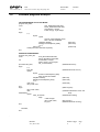
Mod.
V560E
Mod. V265
DTACK
GATE
INT
MON
ADJ
MEMORY
STATUS
RDY
FULL
GATE
CLR
BUSY
TEST
0
1
2
I
N
P
U
T
S
3
4
5
6
7
8 CH
CIA
Fig. 1.2 – Mod. V265 Front panel
Filename:
V265_REV0.DOC
Number of pages:
16
Page:
5
Document type:
User's Manual (MUT)
Title:
Mod. V265 8 channel charge integrating ADC
Revision date:
20/04/99
Revision:
0
2. Specifications
2.1.
Packaging
1-unit wide VME module.
2.2.
External components
CONNECTORS:
−No. 8 LEMO 00 type "INPUTS 0..7". Input connectors 0 to 7.
−No. 1 LEMO 00 type (or ECL type) "GATE". GATE signal input connector.
−No. 1 LEMO 00 type (or ECL type) "CLR". CLEAR signal input connector.
−No. 1 LEMO 00 type (or ECL type) "BUSY". BUSY signal output connector.
−No. 1 LEMO 00 type"TEST". TEST signal input connector.
DISPLAYS:
−No. 1 red LED "FULL". It lights up whenever the module's FIFO memory is full.
−No. 1 green LED "RDY". It lights up if the module's FIFO memory contains at least a
valid datum.
−No. 1 red LED "DTACK". It lights up during a VME access.
TEST POINTS:
−No. 1 "GATE INT MON". Internal GATE monitoring.
TRIMMERS:
−No. 1 screw-driver trimmer "GATE INT ADJ". For the internal GATE width adjustment.
2.3.
Internal Components
FUSES:
−F1: +5 V, 5 A (trinitron type);
−F2: +12 V, 2 A (trinitron type);
−F3: −12 V, 2 A (trinitron type).
Filename:
V265_REV0.DOC
Number of pages:
16
Page:
6
Document type:
User's Manual (MUT)
Title:
Mod. V265 8 channel charge integrating ADC
Revision date:
20/04/99
Revision:
0
JUMPERS:
−JP1: a two-position jumper dedicated to the selection of the interrupt generation
according to the FIFO memory state (NO EMPTY or FULL).
−JP2: a two-position jumper dedicated to the selection of an internal or external TEST
signal.
SWITCHES:
−No. 4 rotary switches for the Module's Base Address selection.
2.4.
Characteristics of the signals
INPUTS:
−signals to be converted (INPUTS 0 to 7): positive or negative polarity and AC/DC
coupled on request. 50Ω impedance;
−GATE and CLEAR: V 265E: ECL differential 110 Ω impedance;
V 265N: standard NIM level 50Ω impedance;
−TEST:
same as the signals to be converted (negative polarity only).
15K Ω impedance.
OUTPUTS:
-BUSY:
V 265E: ECL differential.
V 265N: TTL level, open collector, negative logic.
-GATE INT MON:
2.5.
ECL level, positive logic.
Performances and test results
−Input impedance: 50Ω ±1.5%.
−Input offset voltage: ± 2 mV.
−Input range: −1.5 V to +5 mV for linear response (negative input).
−Full scale: ≈120 pC (15 bits ADC range), ≈800 pC (12 bits ADC range).
−Conversion gain: ≈30 counts/pC (15 bit ADC range), ≈4 counts/pC (12 bit ADC range).
−Gain dispersion: ±2 counts/pC max.
−Gain variations versus relative timing input to GATE: 1.05%.
−Integral non linearity (see page 9): within ±7 counts (15 bit ADC range), ±2.5 counts (12 bit
ADC range).
−Gate width: 100 ns to 5 µs.
Filename:
V265_REV0.DOC
Number of pages:
16
Page:
7
Document type:
User's Manual (MUT)
Title:
Mod. V265 8 channel charge integrating ADC
Revision date:
20/04/99
Revision:
0
−Gate timing: the GATE signal must precede the analog input by ≥65 ns.
−FAST CLEAR width: ≥30 ns. The pedestal settles with ± 1 count after 200 ns (12 bits).
−Conversion time: 300 µs/8-ch.
−test sensitivity: ≈30 times less than a channel.
−Pedestal/GATE width: ≈50 counts/100 ns (15 bit ADC range), ≈7 counts/100 ns (12 bit ADC
range).
−Residual pedestal: ≈50 counts (15 bit ADC range), ≈7 counts (12 bit ADC range) (for a GATE
width of 300 ns and a high source impedance).
−Temperature coefficient: + 0.15% or + 3 counts/°C max.
2.6.
Power requirements
+5
2.62 A.
−12 V
25 mA.
+12 V
102 mA.
Filename:
V265_REV0.DOC
Number of pages:
16
Page:
8
Document type:
User's Manual (MUT)
2.7.
Title:
Mod. V265 8 channel charge integrating ADC
Revision date:
20/04/99
Revision:
0
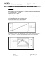
Integral non linearity test procedure performed by CAEN
PROCEDURE
1.On the V 265 printed-circuit board, set the JP3 jumper to "INT" position: the module's internal
DAC is enabled to supply the CVC inputs with an appropriate signal and an internal GATE signal
can be generated (see 5
Test logic).
2.Set the GATE width to ≈400 ns.
3.By performing a WRITE operation, set the DAC register to an initial voltage value.
4.Read "i" ADC output values (where i = 1 to 50) and calculate the corresponding ηi (medium
value) and σi (standard deviation).
5.Increase the DAC voltage value and repeat the step 4.
6.Repeat step 5 until 50 ηi and σi values are obtained.
7.Calculate the corresponding Best Fit Line (BFL):
8.Calculate the maximum value (Max) of [(BFLi−ηi)+2σi] and the minimum value (Min) of
[(BFLi−ηi)−2σi]where i = 1 to 50. The maximum integral non linearity value is: (Max-Min)/2
Filename:
V265_REV0.DOC
Number of pages:
16
Page:
9
Document type:
User's Manual (MUT)
Title:
Mod. V265 8 channel charge integrating ADC
Revision date:
20/04/99
Revision:
0
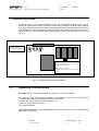
3. Operating mode
The Model V 265 is an A24-D16 VME slave and it can be operated in Data Space, User or
Supervisor mode. Before using the module it is necessary to select the module's Base Address
(in a range from 0000XXH to FFFFXXH) and on which condition of the internal FIFO memory a
VME INTERRUPT will be generated. For this purpose, the module's printed circuit board is
provided with four rotary switches (Base Address selection) and a jumper labelled "JP1" (see
Fig. 3.1).
Rotary switches for
Base Address Selection
MSD
LSD
JP1 set to NE position :
Interrupt generation as soon as the FIFO
contains a valid datum.
JP1 set to F position :
Interrupt generation as soon as the FIFO
is full.
Fig. 3.1 – Rotary Switch and Jumper Position
3.1.
Operations to be performed
CAUTION: Turn OFF the VME crate before inserting or removing the module.
1.By using the four rotary switches located on the module's printed circuit board, set the
module's Base Address as required (0000XXH to FFFFXXH).
2.Set the JP1 internal jumper as required (see Fig. 3.1).
3.Insert the module into a VME slot.
4.Turn ON the System.
THE MODULE IS READY TO BE OPERATED VIA VME (see Table 3.1 for the module's internal
addresses specifications).
Filename:
V265_REV0.DOC
Number of pages:
16
Page:
10
Document type:
User's Manual (MUT)
Title:
Mod. V265 8 channel charge integrating ADC
Revision date:
20/04/99
Revision:
0
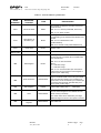
Table 3.1 –Internal Address Specifications
BASE
ADDRESS +
REGISTER/
CONTENT
TYPE
EXPLANATION
This register contains the module's version and
series number.
FEH
Version & Series
READ
Bits 15 to 12: Version (0000=NIM; 0001=ECL).
Bits 11 to 0: Series number.
FCH
This register contains the binary codes
corresponding to the module's manufacturer and
model.
Manufacturer &
Module's Type
READ
Bits 15 to 10: Manufacturer code
(CAEN=000010).
Bits 9 to 0: Module Code (V265=0000010010).
FAH
Fixed Code
READ
F8H to 0AH
UNUSED
///
HFAF5 code
/////
This register contains a channel number, an ADC
number and the converted value correlated with
the channel itself.
Bits 15 to 13: channel number.
08H
Data Register
READ
Bit 12:
0→12 bit ADC range
1→15 bit ADC range
Bits 11 to 0: converted value (the read value is
valid if RDY bit of the Status/Control Register is
equal to1[see Table 3.2]).
06H
Gate Generation
READ/WRITE
04H
DAC Register
WRITE
02H
Clear
READ/WRITE
An R/W operation generates an internal GATE
signal. The GATE width can be set by the GATE
INT ADJ trimmer located on the module's front
panel and it can be monitored by an oscilloscope
connected with the GATE INT MON test point
(ECL signal, positive logic).
Internal DAC setting (see 5
Test logic).
An R/W operation resets the module (the CVCs
and the internal registers are initialized and the
FIFO memory is cleared)
The same result can be obtained by sending a
NIM level signal to the CLR front panel connector.
00H
Status/Control
Register
READ/WRITE
Filename:
V265_REV0.DOC
See Table 3.2
Number of pages:
16
Page:
11
Document type:
User's Manual (MUT)
Title:
Mod. V265 8 channel charge integrating ADC
Revision date:
20/04/99
Revision:
0
Table 3.2 –Status/Control Register Configuration
BIT
CONTENT
TYPE
15
RDY (RDY=1 if FIFO=no empty)
READ
14
FULL (FULL=1 if FIFO=full)
READ
13 to 11
UNUSED
10 to 8
INTERRUPT Level
000=INTERRUPT disabled
(001 to 111)=INTERRUPT levels
READ/WRITE
7 to 0
INTERRUPT Vector
According to the JP1 position, an INTERRUPT can
be generated either when the FIFO memory is no
empty or when the FIFO itself is full. The
INTERRUPT is RORA (Reset On Register Access)
type and it is reset whenever the RUDY or FULL bit
(according to the JP1 position) of the
Status/Control Register becomes FALSE.
READ/WRITE
Filename:
V265_REV0.DOC
Number of pages:
16
Page:
12
Document type:
User's Manual (MUT)
3.2.
Title:
Mod. V265 8 channel charge integrating ADC
Revision date:
20/04/99
Revision:
0
Software programs example
FIFO MANAGEMENT IN POLLING MODE:
program read_ADC;
const
STS_REG=Base Addr+00H;
DATA_REG=Base Addr+08H;
var
STATE,RDY,i: integer;
buffer: array[1..16] of integer;
begin
i:=1;
repeat
repeat
STATE:=memread(STS_REG);
RDY:=STATE and 8000H
until(RDY=8000H);
buffer[i]=memread(DATA_REG);
i:=i+1;
until (i=16);
writeln('One event has been acquired');
end.
INTERRUPT MANAGEMENT:
program read_ADC_INT;
const
STS_REG=BaseAddr+00H;
DATA_REG=Base Addr+08H;
var
STATE,RDY,i: integer;
buffer: array[1..16] of integer;
INT_FLAG: boolean;
procedure INT_DRV;
begin
i:=1;
DIS_INT;
repeat
repeat
STATE:=memread(STS_REG);
RDY:=STATE and 8000H
until(RDY=8000H);
buffer[i]=memread(DATA_REG);
i:=i+1
until (i=16);
INT_FLAG:=true;
end;
begin
INT_FLAG:=false;
INIT;
INTERRUPT
repeat
if INT_FLAG then
begin
<data storage>
INT_FLAG:=false;
EN_INT
end;
.
.
until false;
end.
{RDY test}
{data read}
{buffer=full}
{INTERRUPT driver}
{INTERRUPT level set to 0}
{RDY test}
{data read}
{buffer=full}
{Main Program}
{Initialize INTERRUPT vector and
level}
{INTERRUPT waiting}
{flag recovery}
{INTERRUPT level recovery}
.
Filename:
V265_REV0.DOC
Number of pages:
16
Page:
13
Document type:
User's Manual (MUT)
Title:
Mod. V265 8 channel charge integrating ADC
Revision date:
20/04/99
Revision:
0
4. Calibration operations
The operations to be performed to calibrate the module are listed in the following paragraph 4.2.
As an example we have used the V 265 N version.
The module must be inserted into a VME slot and the system has to be power supplied.
4.1.
Necessary instruments
- No. 1 Pulse Generator capable of producing standard NIM (or ECL) level signals.
- No. 1 Voltmeter.
- No. 1 Oscilloscope.
4.2.
Operations to be performed
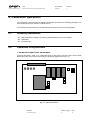
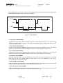
1. GATEH AND CLEARH LEVEL ADJUSTMENT
Via Pulse Generator, send a 1 µ s wide NIM pulse to the GATE connector and a 300 ns wide
NIM pulse to the CLR connector according to the timing diagram (see Fig. 4.2).
U1
P3
P2
P4
P1
U13
U43
R37
U22
R38
Fig. 4.1 – Internal Trimmers
Filename:
V265_REV0.DOC
Number of pages:
16
Page:
14
Document type:
User's Manual (MUT)
Title:
Mod. V265 8 channel charge integrating ADC
Revision date:
20/04/99
Revision:
0
On the piggy-back card, turn the P1 trimmer until a signal which has about the same GATE signal width,
but that switches between 0 and +12/13 Volt, is obtained.
CLEAR
300 ns
GATE
1 µs
1 µs
300 µs
Fig. 4.2 – Timing Diagram
2. U13 OFFSET ADJUSTMENT
Supply the CLR input with a NIM level signal (−800 mV). Connect the voltmeter to U13 - pin 6 and U13
- pin 3. Turn the P1 trimmer located on the printed circuit board until the voltage value shown on the
voltmeter is equal to zero.
3. U22 OFFSET ADJUSTMENT
Supply the CLR input with a NIM level signal (−800 mV). Connect the voltmeter to U22 - pin 6 and to
ground. Turn the P2 trimmer until the voltage value shown on the voltmeter is equal to zero.
4. U1 OFFSET ADJUSTMENT
Supply the CLR input with a NIM level signal (−800 mV). Connect the voltmeter to U1 - pin 6 and to
ground. Turn the P3 trimmer until the voltage value shown on the voltmeter is equal to zero.
5. PEDESTAL ADJUSTMENT
Via Pulse Generator send a 1 µs wide NIM pulse to the GATE connector. Read the ADC1 conversion
value and turn the P4 trimmer until the read value is ≅75. The pedestal is now set to
≈7.5 counts/100 ns (12 bit ADC range).
6. DAC OFFSET ADJUSTMENT
Load the module's DAC with 000H. Connect the voltmeter to U43 - pin 6 and to ground. Turn the R38
trimmer until the voltage value shown on the voltmeter is equal to zero.
7. DAC FULL SCALE ADJUSTMENT
Load the module's DAC with FFFH. Connect the voltmeter to U43 - pin 6 and to ground. Turn the R37
trimmer until the voltage value shown on the voltmeter is equal to -9 V .
Filename:
V265_REV0.DOC
Number of pages:
16
Page:
15
Document type:
User's Manual (MUT)
5.
Title:
Mod. V265 8 channel charge integrating ADC
Revision date:
20/04/99
Revision:
0
Test logic
The module is provided with a test circuitry capable of producing an internal GATE signal via
software by performing an R/W operation addressed to the Base Address+06H module's location.
The internal GATE width is adjustable (through the front panel trimmer GATE INT ADJ) in a range
from 400 ns to 2 µs, and it can be monitored by an oscilloscope connected to the GATE INT MON
test point (ECL level, positive logic).
A 12-bit DAC supplies the CVC inputs with an appropriate signal according to the following
formula:
Q ≅ ((9 x TGATE) ÷ (15000 x 4095)) x DAC
Where Q=INPUT CHARGE (Coulomb), TGATE=internal GATE width (seconds) and
DAC=binary code of the voltage value set to the DAC Register by a WRITE operation.
The DAC Register content generates a voltage value according to the following formula:
V = (9 ÷ 4095) x DAC
where DAC can vary in a range from 0 to 4095.Instead of using the internal DAC, it is also
possible to supply the CVC inputs with a common charge through the front panel connector
TEST. An internal jumper (JP3) allows the user to select the required operating mode (see Fig.
5.1)
JP3 set to INT position:
the internal DAC is selected
as signal source.
JP3
JP3 set to EXT position:
an external signal source is
selected (via TEST connector)
Fig. 5.1 – Internal Jumper J3 position
Filename:
V265_REV0.DOC
Number of pages:
16
Page:
16