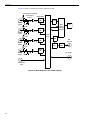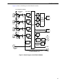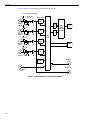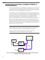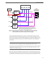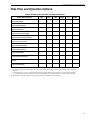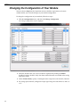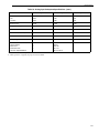
1
Title Page
UM-22417-L
DT9837 Series
User’s Manual
Copyright Page
Eleventh Edition
June, 2010
Copyright © 2006 - 2010 by Data Translation, Inc.
All rights reserved.
Information furnished by Data Translation, Inc. is believed to be
accurate and reliable; however, no responsibility is assumed by
Data Translation, Inc. for its use; nor for any infringements of
patents or other rights of third parties which may result from its
use. No license is granted by implication or otherwise under any
patent rights of Data Translation, Inc.
Use, duplication, or disclosure by the United States Government
is subject to restrictions as set forth in subparagraph (c)(1)(ii) of
the Rights in Technical Data and Computer software clause at 48
C.F.R, 252.227-7013, or in subparagraph (c)(2) of the Commercial
Computer Software - Registered Rights clause at 48 C.F.R.,
52-227-19 as applicable. Data Translation, Inc., 100 Locke Drive,
Marlboro, MA 01752.
Data Translation, Inc.
100 Locke Drive
Marlboro, MA 01752-1192
(508) 481-3700
www.datatranslation.com
Fax: (508) 481-8620
E-mail: [email protected]
Data Translation® is a registered trademark of Data Translation,
Inc. Measure Foundry™, DT-Open LayersTM, DT-Open Layers for
.NET Class LibraryTM, DataAcq SDKTM, LV-LinkTM, and DTx-EZTM
are trademarks of Data Translation, Inc.
All other brand and product names are trademarks or registered
trademarks of their respective companies.
FCC
Page
Radio and Television Interference
This equipment has been tested and found to comply with CISPR EN55022 Class A and
EN61000-6-1 requirements and also with the limits for a Class A digital device, pursuant to
Part 15 of the FCC Rules. These limits are designed to provide reasonable protection against
harmful interference when the equipment is operated in a commercial environment. This
equipment generates, uses, and can radiate radio frequency energy and, if not installed and
used in accordance with the instruction manual, may cause harmful interference to radio
communications. Operation of this equipment in a residential area is likely to cause harmful
interference, in which case the user will be required to correct the interference at his own
expense.
Changes or modifications to this equipment not expressly approved by Data Translation could
void your authority to operate the equipment under Part 15 of the FCC Rules.
Note: This product was verified to meet FCC requirements under test conditions that
included use of shielded cables and connectors between system components. It is important
that you use shielded cables and connectors to reduce the possibility of causing interference
to radio, television, and other electronic devices.
Canadian Department of Communications Statement
This digital apparatus does not exceed the Class A limits for radio noise emissions from
digital apparatus set out in the Radio Interference Regulations of the Canadian Department of
Communications.
Le présent appareil numérique n’émet pas de bruits radioélectriques dépassant les limites
applicables aux appareils numériques de la class A prescrites dans le Règlement sur le
brouillage radioélectrique édicté par le Ministère des Communications du Canada.
Table of Contents
Table of Contents
About this Manual . . . . . . . . . . . . . . . . . . . . . . . . . . . . . . . . . . . . . . . . . . . . . . . . . . . . . . 9
Intended Audience. . . . . . . . . . . . . . . . . . . . . . . . . . . . . . . . . . . . . . . . . . . . . . . . . . . . . . . . . . . . . 9
How this Manual is Organized . . . . . . . . . . . . . . . . . . . . . . . . . . . . . . . . . . . . . . . . . . . . . . . . . . 9
Conventions Used in this Manual . . . . . . . . . . . . . . . . . . . . . . . . . . . . . . . . . . . . . . . . . . . . . . . 10
Related Information . . . . . . . . . . . . . . . . . . . . . . . . . . . . . . . . . . . . . . . . . . . . . . . . . . . . . . . . . . . 10
Where To Get Help. . . . . . . . . . . . . . . . . . . . . . . . . . . . . . . . . . . . . . . . . . . . . . . . . . . . . . . . . . . . 11
Chapter 1: Overview . . . . . . . . . . . . . . . . . . . . . . . . . . . . . . . . . . . . . . . . . . . . . . . . . . . 13
Hardware Features . . . . . . . . . . . . . . . . . . . . . . . . . . . . . . . . . . . . . . . . . . . . . . . . . . . . . . . . . . . 14
Key Features of the DT9837 . . . . . . . . . . . . . . . . . . . . . . . . . . . . . . . . . . . . . . . . . . . . . . . . . 14
Key Features of the DT9837A . . . . . . . . . . . . . . . . . . . . . . . . . . . . . . . . . . . . . . . . . . . . . . . 15
Key Features of the DT9837B. . . . . . . . . . . . . . . . . . . . . . . . . . . . . . . . . . . . . . . . . . . . . . . . 16
Supported Software . . . . . . . . . . . . . . . . . . . . . . . . . . . . . . . . . . . . . . . . . . . . . . . . . . . . . . . . . . . 17
Supported Accessories. . . . . . . . . . . . . . . . . . . . . . . . . . . . . . . . . . . . . . . . . . . . . . . . . . . . . . . . . 19
Getting Started Procedure. . . . . . . . . . . . . . . . . . . . . . . . . . . . . . . . . . . . . . . . . . . . . . . . . . . . . . 20
Part 1: Getting Started . . . . . . . . . . . . . . . . . . . . . . . . . . . . . . . . . . . . . 21
Chapter 2: Setting Up and Installing the Module . . . . . . . . . . . . . . . . . . . . . . . . . . . . 23
Unpacking . . . . . . . . . . . . . . . . . . . . . . . . . . . . . . . . . . . . . . . . . . . . . . . . . . . . . . . . . . . . . . . . . . . 25
Attaching Modules to the Computer. . . . . . . . . . . . . . . . . . . . . . . . . . . . . . . . . . . . . . . . . . . . . 26
Connecting Directly to the USB Ports . . . . . . . . . . . . . . . . . . . . . . . . . . . . . . . . . . . . . . . . 26
Connecting to an Expansion Hub . . . . . . . . . . . . . . . . . . . . . . . . . . . . . . . . . . . . . . . . . . . 27
Configuring the DT9837 Series Device Drivers . . . . . . . . . . . . . . . . . . . . . . . . . . . . . . . . . . . 29
Chapter 3: Wiring Signals . . . . . . . . . . . . . . . . . . . . . . . . . . . . . . . . . . . . . . . . . . . . . . . 31
Preparing to Wire Signals . . . . . . . . . . . . . . . . . . . . . . . . . . . . . . . . . . . . . . . . . . . . . . . . . . . . . . 33
Wiring Recommendations . . . . . . . . . . . . . . . . . . . . . . . . . . . . . . . . . . . . . . . . . . . . . . . . . 33
Wiring Signals to the Module . . . . . . . . . . . . . . . . . . . . . . . . . . . . . . . . . . . . . . . . . . . . . . . 33
Connecting Analog Input Signals . . . . . . . . . . . . . . . . . . . . . . . . . . . . . . . . . . . . . . . . . . . . . . . 35
Connecting an Analog Output Signal . . . . . . . . . . . . . . . . . . . . . . . . . . . . . . . . . . . . . . . . . . . 36
Connecting a Tachometer Input Signal . . . . . . . . . . . . . . . . . . . . . . . . . . . . . . . . . . . . . . . . . . . 37
Connecting a Gate Input Signal . . . . . . . . . . . . . . . . . . . . . . . . . . . . . . . . . . . . . . . . . . . . . . . . . 38
Chapter 4: Verifying the Operation of a Module . . . . . . . . . . . . . . . . . . . . . . . . . . . . . 39
Running the Quick DataAcq Application . . . . . . . . . . . . . . . . . . . . . . . . . . . . . . . . . . . . . . . . 41
Testing Single-Value Analog Input . . . . . . . . . . . . . . . . . . . . . . . . . . . . . . . . . . . . . . . . . . . . . . 42
Testing Continuous Analog Input . . . . . . . . . . . . . . . . . . . . . . . . . . . . . . . . . . . . . . . . . . . . . . . 43
Testing Single-Value Analog Output . . . . . . . . . . . . . . . . . . . . . . . . . . . . . . . . . . . . . . . . . . . . 44
5
Contents
Part 2: Using Your Module. . . . . . . . . . . . . . . . . . . . . . . . . . . . . . . . . . 45
Chapter 5: Principles of Operation . . . . . . . . . . . . . . . . . . . . . . . . . . . . . . . . . . . . . . . 47
Analog Input Features . . . . . . . . . . . . . . . . . . . . . . . . . . . . . . . . . . . . . . . . . . . . . . . . . . . . . . . . . 51
Analog Input Channels . . . . . . . . . . . . . . . . . . . . . . . . . . . . . . . . . . . . . . . . . . . . . . . . . . . . 51
Input Ranges and Gains . . . . . . . . . . . . . . . . . . . . . . . . . . . . . . . . . . . . . . . . . . . . . . . . . . . . 51
IEPE Functions. . . . . . . . . . . . . . . . . . . . . . . . . . . . . . . . . . . . . . . . . . . . . . . . . . . . . . . . . . . . 52
Input Resolution . . . . . . . . . . . . . . . . . . . . . . . . . . . . . . . . . . . . . . . . . . . . . . . . . . . . . . . . . . 52
Input Clock Source . . . . . . . . . . . . . . . . . . . . . . . . . . . . . . . . . . . . . . . . . . . . . . . . . . . . . . . . 52
Analog Input Conversion Modes . . . . . . . . . . . . . . . . . . . . . . . . . . . . . . . . . . . . . . . . . . . . 53
Single-Value Operations . . . . . . . . . . . . . . . . . . . . . . . . . . . . . . . . . . . . . . . . . . . . . . . . 53
Single-Values Operations . . . . . . . . . . . . . . . . . . . . . . . . . . . . . . . . . . . . . . . . . . . . . . . 53
Continuous Scan Mode . . . . . . . . . . . . . . . . . . . . . . . . . . . . . . . . . . . . . . . . . . . . . . . . 54
Input Triggers . . . . . . . . . . . . . . . . . . . . . . . . . . . . . . . . . . . . . . . . . . . . . . . . . . . . . . . . . . . . 55
Data Format and Transfer . . . . . . . . . . . . . . . . . . . . . . . . . . . . . . . . . . . . . . . . . . . . . . . . . . 56
Error Conditions . . . . . . . . . . . . . . . . . . . . . . . . . . . . . . . . . . . . . . . . . . . . . . . . . . . . . . . . . . 57
Analog Output Features . . . . . . . . . . . . . . . . . . . . . . . . . . . . . . . . . . . . . . . . . . . . . . . . . . . . . . . 58
Analog Output Channels . . . . . . . . . . . . . . . . . . . . . . . . . . . . . . . . . . . . . . . . . . . . . . . . . . . 58
Output Ranges and Gains . . . . . . . . . . . . . . . . . . . . . . . . . . . . . . . . . . . . . . . . . . . . . . . . . . 58
Output Resolution. . . . . . . . . . . . . . . . . . . . . . . . . . . . . . . . . . . . . . . . . . . . . . . . . . . . . . . . . 58
Output Clocks . . . . . . . . . . . . . . . . . . . . . . . . . . . . . . . . . . . . . . . . . . . . . . . . . . . . . . . . . . . . 58
Output Conversion Modes . . . . . . . . . . . . . . . . . . . . . . . . . . . . . . . . . . . . . . . . . . . . . . . . . 59
Single-Value Mode . . . . . . . . . . . . . . . . . . . . . . . . . . . . . . . . . . . . . . . . . . . . . . . . . . . . 59
Waveform Generation Mode . . . . . . . . . . . . . . . . . . . . . . . . . . . . . . . . . . . . . . . . . . . . 59
Continuous Analog Output Operations . . . . . . . . . . . . . . . . . . . . . . . . . . . . . . . . . . 60
Reading the Analog Output Value in the Analog Input Data Stream
(DT9837A Module Only) . . . . . . . . . . . . . . . . . . . . . . . . . . . . . . . . . . . . . . . . . . . . . . . . . . 61
Output Trigger . . . . . . . . . . . . . . . . . . . . . . . . . . . . . . . . . . . . . . . . . . . . . . . . . . . . . . . . . . . . 61
Data Format and Transfer . . . . . . . . . . . . . . . . . . . . . . . . . . . . . . . . . . . . . . . . . . . . . . . . . . 62
Error Conditions . . . . . . . . . . . . . . . . . . . . . . . . . . . . . . . . . . . . . . . . . . . . . . . . . . . . . . . . . . 62
Tachometer Input Features . . . . . . . . . . . . . . . . . . . . . . . . . . . . . . . . . . . . . . . . . . . . . . . . . . . . . 63
Frequency or Period Measurements – Tachometer Counter 0 . . . . . . . . . . . . . . . . . . . . 63
Phase Measurements – Tachometer Counter 1 . . . . . . . . . . . . . . . . . . . . . . . . . . . . . . . . . 64
Gate Input Features . . . . . . . . . . . . . . . . . . . . . . . . . . . . . . . . . . . . . . . . . . . . . . . . . . . . . . . . . . . 66
Triggering Acquisition on Multiple Modules . . . . . . . . . . . . . . . . . . . . . . . . . . . . . . . . . . . . . 67
Synchronizing Acquisition on Multiple DT9837A or DT9837B Modules . . . . . . . . . . . . . . 68
Chapter 6: Supported Device Driver Capabilities. . . . . . . . . . . . . . . . . . . . . . . . . . . . 71
Data Flow and Operation Options. . . . . . . . . . . . . . . . . . . . . . . . . . . . . . . . . . . . . . . . . . . . . . . 73
Buffering . . . . . . . . . . . . . . . . . . . . . . . . . . . . . . . . . . . . . . . . . . . . . . . . . . . . . . . . . . . . . . . . . . . . 74
Triggered Scan Mode . . . . . . . . . . . . . . . . . . . . . . . . . . . . . . . . . . . . . . . . . . . . . . . . . . . . . . . . . . 74
Data Encoding. . . . . . . . . . . . . . . . . . . . . . . . . . . . . . . . . . . . . . . . . . . . . . . . . . . . . . . . . . . . . . . . 74
6
Contents
Channels . . . . . . . . . . . . . . . . . . . . . . . . . . . . . . . . . . . . . . . . . . . . . . . . . . . . . . . . . . . . . . . . . . . . 75
Gain . . . . . . . . . . . . . . . . . . . . . . . . . . . . . . . . . . . . . . . . . . . . . . . . . . . . . . . . . . . . . . . . . . . . . . . . 75
Ranges . . . . . . . . . . . . . . . . . . . . . . . . . . . . . . . . . . . . . . . . . . . . . . . . . . . . . . . . . . . . . . . . . . . . . . 76
Resolution . . . . . . . . . . . . . . . . . . . . . . . . . . . . . . . . . . . . . . . . . . . . . . . . . . . . . . . . . . . . . . . . . . . 76
Thermocouple and RTD Support. . . . . . . . . . . . . . . . . . . . . . . . . . . . . . . . . . . . . . . . . . . . . . . . 77
IEPE Support. . . . . . . . . . . . . . . . . . . . . . . . . . . . . . . . . . . . . . . . . . . . . . . . . . . . . . . . . . . . . . . . . 77
Triggers . . . . . . . . . . . . . . . . . . . . . . . . . . . . . . . . . . . . . . . . . . . . . . . . . . . . . . . . . . . . . . . . . . . . . 78
Clocks . . . . . . . . . . . . . . . . . . . . . . . . . . . . . . . . . . . . . . . . . . . . . . . . . . . . . . . . . . . . . . . . . . . . . . . 79
Counter/Timers . . . . . . . . . . . . . . . . . . . . . . . . . . . . . . . . . . . . . . . . . . . . . . . . . . . . . . . . . . . . . . 80
Chapter 7: Using the VIBpoint Framework Application . . . . . . . . . . . . . . . . . . . . . . . 81
Overview . . . . . . . . . . . . . . . . . . . . . . . . . . . . . . . . . . . . . . . . . . . . . . . . . . . . . . . . . . . . . . . . . . . . 82
Running the VIBpoint Framework Application . . . . . . . . . . . . . . . . . . . . . . . . . . . . . . . . . . . 83
Changing the Configuration of Your Module . . . . . . . . . . . . . . . . . . . . . . . . . . . . . . . . . . . . . 86
Acquire, Display, and Record Data . . . . . . . . . . . . . . . . . . . . . . . . . . . . . . . . . . . . . . . . . . . . . . 89
Recording Settings . . . . . . . . . . . . . . . . . . . . . . . . . . . . . . . . . . . . . . . . . . . . . . . . . . . . . . . . 89
Trigger Settings . . . . . . . . . . . . . . . . . . . . . . . . . . . . . . . . . . . . . . . . . . . . . . . . . . . . . . . . . . . 91
Chart Recorder. . . . . . . . . . . . . . . . . . . . . . . . . . . . . . . . . . . . . . . . . . . . . . . . . . . . . . . . . . . . 92
Channel Name . . . . . . . . . . . . . . . . . . . . . . . . . . . . . . . . . . . . . . . . . . . . . . . . . . . . . . . . 93
Channel Visibility . . . . . . . . . . . . . . . . . . . . . . . . . . . . . . . . . . . . . . . . . . . . . . . . . . . . . 93
Show Cursor . . . . . . . . . . . . . . . . . . . . . . . . . . . . . . . . . . . . . . . . . . . . . . . . . . . . . . . . . 93
Signal Group . . . . . . . . . . . . . . . . . . . . . . . . . . . . . . . . . . . . . . . . . . . . . . . . . . . . . . . . . 93
Data Tab . . . . . . . . . . . . . . . . . . . . . . . . . . . . . . . . . . . . . . . . . . . . . . . . . . . . . . . . . . . . . 94
Plot Tab . . . . . . . . . . . . . . . . . . . . . . . . . . . . . . . . . . . . . . . . . . . . . . . . . . . . . . . . . . . . . . 95
Style Tab . . . . . . . . . . . . . . . . . . . . . . . . . . . . . . . . . . . . . . . . . . . . . . . . . . . . . . . . . . . . . 95
FFTs . . . . . . . . . . . . . . . . . . . . . . . . . . . . . . . . . . . . . . . . . . . . . . . . . . . . . . . . . . . . . . . . . 96
Chart Controls . . . . . . . . . . . . . . . . . . . . . . . . . . . . . . . . . . . . . . . . . . . . . . . . . . . . . . . . 96
Device Status . . . . . . . . . . . . . . . . . . . . . . . . . . . . . . . . . . . . . . . . . . . . . . . . . . . . . . . . . 96
Channel Overview . . . . . . . . . . . . . . . . . . . . . . . . . . . . . . . . . . . . . . . . . . . . . . . . . . . . . . . . 96
Exiting from the VIBpoint Framework Application . . . . . . . . . . . . . . . . . . . . . . . . . . . . . . . . 98
Chapter 8: Troubleshooting . . . . . . . . . . . . . . . . . . . . . . . . . . . . . . . . . . . . . . . . . . . . . 99
General Checklist . . . . . . . . . . . . . . . . . . . . . . . . . . . . . . . . . . . . . . . . . . . . . . . . . . . . . . . . . . . . 100
Technical Support . . . . . . . . . . . . . . . . . . . . . . . . . . . . . . . . . . . . . . . . . . . . . . . . . . . . . . . . . . . 102
If Your Module Needs Factory Service . . . . . . . . . . . . . . . . . . . . . . . . . . . . . . . . . . . . . . . . . . 103
Chapter 9: Calibration . . . . . . . . . . . . . . . . . . . . . . . . . . . . . . . . . . . . . . . . . . . . . . . . . 105
Using the Calibration Utility . . . . . . . . . . . . . . . . . . . . . . . . . . . . . . . . . . . . . . . . . . . . . . . . . . 107
Calibrating the Analog Input Subsystem . . . . . . . . . . . . . . . . . . . . . . . . . . . . . . . . . . . . . . . 108
Connecting a Precision Voltage Source . . . . . . . . . . . . . . . . . . . . . . . . . . . . . . . . . . . . . . 108
Using the Auto-Calibration Procedure . . . . . . . . . . . . . . . . . . . . . . . . . . . . . . . . . . . . . . 108
Using the Manual Calibration Procedure . . . . . . . . . . . . . . . . . . . . . . . . . . . . . . . . . . . . 108
Calibrating the Analog Output Subsystem . . . . . . . . . . . . . . . . . . . . . . . . . . . . . . . . . . . . . . 110
7
Contents
Appendix A: Specifications . . . . . . . . . . . . . . . . . . . . . . . . . . . . . . . . . . . . . . . . . . . . 111
Analog Input Specifications . . . . . . . . . . . . . . . . . . . . . . . . . . . . . . . . . . . . . . . . . . . . . . . . . . . 112
Analog Output Specifications. . . . . . . . . . . . . . . . . . . . . . . . . . . . . . . . . . . . . . . . . . . . . . . . . . 114
Tachometer Input Specifications . . . . . . . . . . . . . . . . . . . . . . . . . . . . . . . . . . . . . . . . . . . . . . . 115
Gate Input Specifications . . . . . . . . . . . . . . . . . . . . . . . . . . . . . . . . . . . . . . . . . . . . . . . . . . . . . 116
Trigger Specifications. . . . . . . . . . . . . . . . . . . . . . . . . . . . . . . . . . . . . . . . . . . . . . . . . . . . . . . . . 117
Master Oscillator Specifications . . . . . . . . . . . . . . . . . . . . . . . . . . . . . . . . . . . . . . . . . . . . . . . . 118
Power, Physical, and Environmental Specifications . . . . . . . . . . . . . . . . . . . . . . . . . . . . . . . 119
Regulatory Specifications . . . . . . . . . . . . . . . . . . . . . . . . . . . . . . . . . . . . . . . . . . . . . . . . . . . . . 120
Connector Specifications . . . . . . . . . . . . . . . . . . . . . . . . . . . . . . . . . . . . . . . . . . . . . . . . . . . . . . 121
Appendix B: Connector Pin Assignments . . . . . . . . . . . . . . . . . . . . . . . . . . . . . . . . 123
RJ45 (LVDS) Connector . . . . . . . . . . . . . . . . . . . . . . . . . . . . . . . . . . . . . . . . . . . . . . . . . . . . . . . 124
Gate Input Connector . . . . . . . . . . . . . . . . . . . . . . . . . . . . . . . . . . . . . . . . . . . . . . . . . . . . . . . . 125
Appendix C: Register-Level Programming . . . . . . . . . . . . . . . . . . . . . . . . . . . . . . . . 127
DT9837 Register-Level Programming . . . . . . . . . . . . . . . . . . . . . . . . . . . . . . . . . . . . . . . . . . . 128
Writing to the General Control Register 2 . . . . . . . . . . . . . . . . . . . . . . . . . . . . . . . . . . . . 128
Writing to EEPROM . . . . . . . . . . . . . . . . . . . . . . . . . . . . . . . . . . . . . . . . . . . . . . . . . . . . . . 129
DT9837A and DT9837B Register-Level Programming . . . . . . . . . . . . . . . . . . . . . . . . . . . . . 131
Writing to the General Control Register 4 . . . . . . . . . . . . . . . . . . . . . . . . . . . . . . . . . . . . 131
Writing to EEPROM . . . . . . . . . . . . . . . . . . . . . . . . . . . . . . . . . . . . . . . . . . . . . . . . . . . . . . 132
Index . . . . . . . . . . . . . . . . . . . . . . . . . . . . . . . . . . . . . . . . . . . . . . . . . . . . . . . . . . . . . . . 135
8
About this Manual
The DT9837 Series includes the DT9837, DT9837A, and DT9837B modules. The first part of
this manual describes how to install and set up your DT9837 Series module and device driver,
and verify that your module is working properly.
The second part of this manual describes the features of the DT9837 Series modules, the
capabilities of the DT9837 Series Device Drivers, and how to program the DT9837 Series
modules using the DT-Open Layers for .NET Class Library™ software. Troubleshooting
information is also provided.
Note: For information on checking system requirements, installing the software, and
viewing the documentation, refer to the README file on the OMNI CD.
For more information on the class library, refer to the DT-Open Layers for .NET Class Library
User’s Manual. If you are using the DataAcq SDK or a software application to program your
device, refer to the documentation for that software for more information.
Intended Audience
This document is intended for engineers, scientists, technicians, or others responsible for
using and/or programming a DT9837 Series module for data acquisition operations in the
Microsoft® Windows® XP, Windows Vista®, or Windows 7 operating system. It is assumed
that you have some familiarity with data acquisition principles and that you understand your
application.
How this Manual is Organized
This manual is organized as follows:
• Chapter 1, “Overview,” describes the major features of the DT9837 Series modules, as well
as the supported software and accessories for the modules.
• Chapter 2, “Setting Up and Installing the Module,” describes how to install a DT9837
Series module, how to apply power to the module, and how to configure the DT9837
Series Device Drivers.
• Chapter 3, “Wiring Signals,” describes how to wire signals to a DT9837 Series module.
• Chapter 4, “Verifying the Operation of a Module,” describes how to verify the operation
of a DT9837 Series module with the Quick DataAcq application.
• Chapter 5, “Principles of Operation,” describes all of the features of the DT9837 Series
modules and how to access them in your application.
• Chapter 6, “Supported Device Driver Capabilities,” lists the data acquisition subsystems
and the associated features accessible using the DT9837 Series Device Drivers.
9
About this Manual
• Chapter 7, “Using the VIBpoint Framework Application,” provides information about
using the VIBpoint Framework application with the DT9837 Series modules.
• Chapter 8, “Troubleshooting,” provides information that you can use to resolve problems
with the DT9837 Series modules and DT9837 Series Device Drivers, should they occur.
• Chapter 9, “Calibration,” describes how to calibrate the analog I/O circuitry of the
DT9837 Series modules.
• Appendix A, “Specifications,” lists the specifications of the DT9837 Series modules.
• An index completes this manual.
Conventions Used in this Manual
The following conventions are used in this manual:
• Notes provide useful information or information that requires special emphasis, cautions
provide information to help you avoid losing data or damaging your equipment, and
warnings provide information to help you avoid catastrophic damage to yourself or your
equipment.
• Items that you select or type are shown in bold.
Related Information
Refer to the following documents for more information on using the DT9837 Series modules:
• Benefits of the Universal Serial Bus for Data Acquisition. This white paper describes why USB
is an attractive alternative for data acquisition. It is available on the Data Translation web
site (www.datatranslation.com).
• Measure Foundry Manual (UM-19298) and online help. These documents describe how to
use Measure Foundry™ to build drag-and-drop test and measurement applications for
Data Translation data acquisition devices.
• DT-Open Layers for .NET User’s Manual (UM-22161). For programmers who are developing
their own application programs using Visual C# or Visual Basic .NET, this manual
describes how to use the DT-Open Layers for .NET Class Library to access the capabilities
of Data Translation data acquisition devices.
• DataAcq SDK User’s Manual (UM-18326). For programmers who are developing their own
application programs using the Microsoft C compiler, this manual describes how to use
the DT-Open Layers DataAcq SDK™ to access the capabilities of Data Translation data
acquisition devices.
• LV-Link Online Help. This help file describes how to use LV-Link™ with the LabVIEW™
graphical programming language to access the capabilities of Data Translation data
acquisition devices.
• Microsoft Windows XP, Windows Vista, or Windows 7 documentation.
• USB web site (http://www.usb.org).
10
About this Manual
Where To Get Help
Should you run into problems installing or using a DT9837 Series module, the Data
Translation Technical Support Department is available to provide technical assistance. Refer
to Chapter 8 for more information. If you are outside the United States or Canada, call your
local distributor, whose number is listed on our web site (www.datatranslation.com).
11
About this Manual
12
1
Overview
Hardware Features. . . . . . . . . . . . . . . . . . . . . . . . . . . . . . . . . . . . . . . . . . . . . . . . . . . . . . . . . . . . 14
Supported Software . . . . . . . . . . . . . . . . . . . . . . . . . . . . . . . . . . . . . . . . . . . . . . . . . . . . . . . . . . . 17
Supported Accessories. . . . . . . . . . . . . . . . . . . . . . . . . . . . . . . . . . . . . . . . . . . . . . . . . . . . . . . . . 20
Getting Started Procedure. . . . . . . . . . . . . . . . . . . . . . . . . . . . . . . . . . . . . . . . . . . . . . . . . . . . . . 20
13
Chapter 1
Hardware Features
The DT9837, DT9837A, and DT9837B are high-performance, multifunction data acquisition
modules for the USB (Ver. 2.0 or Ver. 1.1) bus. Table 1 lists the major differences among the
modules.
Table 1: Major Differences Among the DT9837 Series Modules
Feature
DT9837
Maximum A/D Throughput
DT9837A
DT9837B
52.734 kHz
52.734 kHz
105.469 kHz
A/D Threshold Trigger
Fixed
Programmable
Programmable
Number of Tachometer Counters
1
2 (C/T 0 and 1)
2 (C/T 0 and 1)
Number of Gate Inputs
0
1b (C/T 2)
1c (C/T 2)
Number of Analog Output
Channels
1
1
0
Analog Output Readback
Capability
No
Yes
No
Analog Output Trigger Types
Software trigger only
Software trigger,
external digital trigger, or
analog threshold trigger
None
RJ45 Synchronization Connector
No
Yes
Yes
a
a. On the DT9837, the threshold level is fixed at 1.0 V. On the DT9837A and DT9837B, the analog threshold level is
programmable from 0.2 V to 9.8 V with 0.1 V of hysteresis.
b. Available on the DT9837A-OEM version.
c. Available through a BNC connector on the DT9837B module.
Key Features of the DT9837
The key hardware features of the DT9837 module are as follows:
• Simultaneous analog input and waveform analog output operations
• Analog input subsystem:
− Four, simultaneous 24-bit A/D converters
− Throughput rate up to 52.734 kSamples/s for simultaneous, high-resolution
measurements
− Input range of ±10 V with software-selectable gains of 1 and 10 for an effective input
range of ±10 V and ±1 V
− Support for IEPE (Integrated Electronic Piezoelectric) inputs, including use of a 4 mA
current source and AC or DC coupling
− The ability to return the value of tachometer counter 0 in the analog input data stream,
allowing you to measure the period or frequency of the tachometer input signal
synchronously with analog input measurements
14
Overview
− Software-programmable trigger type (software, external digital trigger, or analog
threshold trigger) to start the analog input operation.
• Analog output subsystem:
− One 24-bit D/A converter
− Waveform capability of up to 8,192 sample
− Output rate of 46.875 kSamples/s
− Output range of ±10 V
− A software trigger starts the analog output operation
• Internal clock source (shared between the analog input and analog output subsystems)
Key Features of the DT9837A
The key hardware features of the DT9837A module are as follows:
• Simultaneous analog input and waveform analog output operations
• Analog input subsystem:
− Four, simultaneous 24-bit A/D converters
− Throughput rate up to 52.734 kSamples/s for simultaneous, high-resolution
measurements
− Input range of ±10 V with software-selectable gains of 1 and 10 for an effective input
range of ±10 V and ±1 V
− Support for IEPE (Integrated Electronic Piezoelectric) inputs, including use of a 4 mA
current source and AC or DC coupling
− The ability to return the value of tachometer counter 0 in the analog input data stream,
allowing you to measure the period or frequency of the tachometer input signal
synchronously with analog input measurements
− The ability to read the value of tachometer counter 1 in the analog input data stream,
allowing you to precisely correlate tachometer measurements with analog input
measurements
− Optional OEM version of this module, called the DT9837A-OEM, supports the ability
to read the value of gate counter 2 in the analog input data stream, allowing you to
precisely correlate gate input measurements with analog input measurements
− Supports reading analog output values in the analog input data stream, allowing you
to correlate input and output values
− Software-programmable trigger type (software, external digital trigger, or analog
threshold trigger) to start the analog input operation. You can also program the analog
input threshold value.
• Analog output subsystem:
− One 24-bit D/A converter
− Single value, waveform, and continuous streaming output
− Programmable output rate from 10 kSamples/s to 52.734 kSamples/s
15
Chapter 1
− Output range of ±10 V
− Software-programmable trigger type (software trigger, external digital trigger, or
analog threshold trigger) to start the analog output operation. You can also program
the threshold value.
• Internal clock source (shared between the analog input and analog output subsystems)
• RJ45 synchronization (LVDS) connector for synchronizing acquisition on up to four
DT9837A modules
Key Features of the DT9837B
The key hardware features of the modules are as follows:
• Four, simultaneous 24-bit A/D converters
• Internal clock source with a throughput rate up to 105.469 kSamples/s for simultaneous,
high-resolution analog input measurements
• Input range of ±10 V with software-selectable gains of 1 and 10 for an effective input
range of ±10 V and ±1 V
• Support for IEPE (Integrated Electronic Piezoelectric) inputs, including use of a 4 mA
current source and AC or DC coupling
• The ability to return the value of tachometer counter 0 in the analog input data stream,
allowing you to measure the period or frequency of the tachometer input signal
synchronously with analog input measurements
• The ability to read the value of tachometer counter 1 in the analog input data stream,
allowing you to precisely correlate tachometer measurements with analog input
measurements
• The ability to read the value of gate counter 2 in the analog input data stream, allowing
you to precisely correlate gate input measurements with analog input measurements
• Software-programmable trigger type (software, external digital trigger, or analog
threshold trigger) to start the analog input operation. You can also program the analog
input threshold value.
• RJ45 synchronization (LVDS) connector for synchronizing acquisition on up to four
DT9837B modules
16
Overview
Supported Software
The following software is available for use with the DT9837 Series modules and is included on
the Data Acquisition OMNI CD:
• DT9837 Series Device Drivers – Two device drivers are provided in the DT9837 Series:
one for the DT9837 module and one for the DT9837A and DT9837B module. The DT9837
Series Device Drivers allow you to use a DT9837, DT9837A, or DT9837B module with any
of the supported software packages or utilities.
• VIBpoint Framework application – A 14-day trial version of this application is shipped
with the DT9837 Series modules. This application, described in Chapter 7, lets you do the
following:
− Discover and select available DT9837 Series modules
− Configure your DT9837 Series modules
− Acquire data from multiple DT9837A, DT9837A-OEM, and DT9837-B modules
− Display acquired data during acquisition
− Perform FFTs (Fast Fourier Transforms) on the acquired analog input data
− Use a chart recorder to display snapshot or snapshots of data and log it to disk for later
analysis
− Use the channel overview to view data from your instrument module as a digital
display
• Quick DataAcq application – The Quick DataAcq application provides a quick way to get
up and running using a DT9837 Series module. Using this application, you can verify key
features of the modules, display data on the screen, and save data to disk. (Note that this
application does not support configuring AC/DC coupling or the excitation current
source for IEPE inputs.)
• The quickDAQ application – An evaluation version of this .NET application is included
on the Data Acquisition OMNI CD. quickDAQ lets you acquire analog data from all
devices supported by DT-Open Layers for .NET software at high speed, plot it during
acquisition, analyze it, and/or save it to disk for later analysis.
• Measure Foundry – An evaluation version of this software is included or provided via a
link on the Data Acquisition OMNI CD. Measure Foundry is a drag-and-drop test and
measurement application builder designed to give you top performance with ease-of-use
development. Order the full development version of this software package to develop
your own application using real hardware.
• DT-Open Layers for .NET Class Library – Use this class library if you want to use Visual
C# or Visual Basic for .NET to develop your own application software for a DT9837 Series
module using Visual Studio 2003 or Visual Studio 2005; the class library complies with the
DT-Open Layers standard.
• DataAcq SDK – Use the Data Acq SDK if you want to use Visual Studio 6.0 and Microsoft
C or C++ to develop your own application software for a DT9837 Series module using
Windows XP, Windows Vista, or Windows 7; the DataAcq SDK complies with the
DT-Open Layers standard.
17
Chapter 1
• DAQ Adaptor for MATLAB – Data Translation’s DAQ Adaptor provides an interface
between the MATLAB Data Acquisition (DAQ) subsystem from The MathWorks and Data
Translation’s DT-Open Layers architecture.
• LV-Link – An evaluation version of LV-Link is included on the Data Acquisition OMNI
CD. Use LV-Link if you want to use the LabVIEW graphical programming language to
access the capabilities of the DT9837 Series module.
Refer to the Data Translation web site (www.datatranslation.com) for information about
selecting the right software package for your needs.
18
Overview
Supported Accessories
The following accessory is available for use with the DT9837A and DT9837B modules:
• EP386 panel – This RJ45 distribution panel contains four RJ45 connectors that are wired in
parallel, making it useful when attaching up to four DT9837A or DT9837B modules
together. Refer to page 69 for more information on using this panel.
Note: You must have revision H or later of the DT9837A module or revision F or later of the
DT9837A-OEM module to be able to attach four modules together. You can identify the
revision of your module by looking at the serial number label on your module.
If you have revision G or earlier of the DT9837A or revision E or earlier of the
DT9837A-OEM, you can attach a maximum of two modules together.
19
Chapter 1
Getting Started Procedure
The flow diagram shown in Figure 1 illustrates the steps needed to get started using a DT9837
Series module. This diagram is repeated in each Getting Started chapter; the shaded area in
the diagram shows you where you are in the getting started procedure.
Set Up and Install the Module
(see Chapter 2 starting on page 23)
Wire Signals
(see Chapter 3 starting on page 31)
Verify the Operation of the Module
(see Chapter 4 starting on page 39)
Figure 1: Getting Started Flow Diagram
20
Part 1: Getting Started
2
Setting Up and Installing the Module
Unpacking . . . . . . . . . . . . . . . . . . . . . . . . . . . . . . . . . . . . . . . . . . . . . . . . . . . . . . . . . . . . . . . . . . . 25
Attaching Modules to the Computer. . . . . . . . . . . . . . . . . . . . . . . . . . . . . . . . . . . . . . . . . . . . . 26
Configuring the DT9837 Series Device Drivers . . . . . . . . . . . . . . . . . . . . . . . . . . . . . . . . . . . . 29
23
Chapter 2
Set Up and Install the Module
(this chapter)
Wire Signals
(see Chapter 3 starting on page 31)
Verify the Operation of the Module
(see Chapter 4 starting on page 39)
24
Setting Up and Installing the Module
Unpacking
Open the shipping box and verify that the following items are present:
• DT9837, DT9837A, or DT9837B module
• EP365 USB cable
• Data Acquisition OMNI CD-ROM
If an item is missing or damaged, contact Data Translation. If you are in the United States, call
the Customer Service Department at (508) 481-3700, ext. 1323. An application engineer will
guide you through the appropriate steps for replacing missing or damaged items. If you are
located outside the United States, call your local distributor, listed on Data Translation’s web
site (www.datatranslation.com).
Note: The DT9837 Series modules are factory-calibrated. If you decide that you want to
recalibrate the analog input or analog output circuitry, refer to the instructions in Chapter 9.
25
Chapter 2
Attaching Modules to the Computer
This section describes how to attach a DT9837 Series module to the host computer.
Note: Most computers have several USB ports that allow direct connection to USB devices.
If your application requires more DT9837 Series modules than you have USB ports for, you
can expand the number of USB devices attached to a single USB port by using expansion
hubs. For more information, refer to page 27.
You can unplug a module, then plug it in again, if you wish, without causing damage. This
process is called hot-swapping. Your application may take a few seconds to recognize a
module once it is plugged back in.
The DT9837 Series modules use less than 500 mA; therefore, they do not require an external
power supply.
You must install the device driver for your module before connecting the module(s) to the
host computer. Run the installation program on your Data Acquisition OMNI CD to install the
device driver and other software for the module.
Connecting Directly to the USB Ports
To connect a DT983 Series module directly to a USB port on your computer, do the following:
1. Attach one end of the USB cable to the USB port on the module.
2. Attach the other end of the USB cable to one of the USB ports on the host computer, as
shown in Figure 2.
The operating system automatically detects the USB module and starts the Found New Hardware
wizard.
DT9837 Series Module
USB Ports
Host Computer
USB Cable
Figure 2: Attaching the Module to the Host Computer
26
Setting Up and Installing the Module
3. For Windows Vista:
a. Click Locate and install driver software (recommended).
The popup message "Windows needs your permission to continue" appears.
b. Click Continue.
The Windows Security dialog box appears.
c.
Click Install this driver software anyway.
For Windows XP:
a. Click Next and/or Finish as required in the wizard.
Once the firmware is loaded, the wizard restarts to initiate the firmware to accept commands.
b. Click Next and/or Finish again.
Note: Windows 7 finds the device automatically.
4. Repeat these steps to attach another DT9837 Series module to the host computer, if
desired.
Note: Once you have connected your module to the host computer, power is turned on to
the module when your application program opens the module. The LED on the module turns
green to indicate that power is turned on.
Power is turned off to the module when your application program terminates its connection
to the module.
Connecting to an Expansion Hub
Expansion hubs are powered by their own external power supply. The practical number of
DT9837 Series modules that you can connect to a single USB port depends on the throughput
you want to achieve.
To connect multiple DT9837 Series modules to an expansion hub, do the following:
1. Attach one end of the USB cable to the module and the other end of the USB cable to an
expansion hub.
2. Connect the power supply for the expansion hub to an external power supply.
3. Connect the expansion hub to the USB port on the host computer using another USB
cable.
The operating system automatically detects the USB module and starts the Found New Hardware
wizard.
4. For Windows Vista:
a. Click Locate and install driver software (recommended).
The popup message "Windows needs your permission to continue" appears.
27
Chapter 2
b. Click Continue.
The Windows Security dialog box appears.
c.
Click Install this driver software anyway.
For Windows XP:
a. Click Next and/or Finish as required in the wizard.
Once the firmware is loaded, the wizard restarts to initiate the firmware to accept commands.
b. Click Next and/or Finish again.
Note: Windows 7 finds the device automatically.
5. Repeat these steps until you have attached the number of expansion hubs and modules
that you require. Refer to Figure 3.
The operating system automatically detects the USB devices as they are installed.
DT9837 Series
Module
DT9837 Series
Module
USB Cables
Host Computer
USB Cable
USB Cable
Power Supply
for Hub
Expansion Hubs
Power Supply
for Hub
DT9837 Series
Module
DT9837 Series
Module
USB Cables
Figure 3: Attaching Multiple Modules Using Expansion Hubs
Note: Once you have connected your module to the host computer, power is turned on to
the DT9837 Series module when your application program opens the module. The LED on
the module turns green to indicate that power is turned on.
Power is turned off to the module when your application program terminates its connection
to the module.
28
Setting Up and Installing the Module
Configuring the DT9837 Series Device Drivers
To configure the device driver for the DT9837, DT9837A, or DT9837B module, do the
following:
1. If you have not already done so, power up the host computer and all peripherals.
2. From the Windows Start menu, select Settings|Control Panel.
3. From the Control Panel, double-click Open Layers Control Panel.
The Data Acquisition Control Panel dialog box appears.
4. If you want to rename the module, click the name of the module that you want to rename,
click Edit Name, enter a new name for the module, and then click OK. The name is used
to identify the module in all subsequent applications.
5. Select the module that you want to configure, and then click Advanced.
The Measurement Options dialog box appears.
6. For the Coupling type, select AC for AC coupling or DC for DC coupling.
7. For the Current Source, select Enabled to enable the 4 mA current source or Disabled to
disable the 4 mA current source.
Note: If you enable the use of the internal 4 mA excitation current source, it is
recommended that you choose AC coupling. Refer to page 35 for more information on
wiring IEPE inputs.
8. You can read the number of counts between two consecutive starting edges of the
tachometer input signal by including channel 4 (tachometer counter 0) in the analog input
channel list. On the DT9837 module, the starting edge is always rising; on the DT9837A
and DT9837B module, the starting edge is programmable (either rising or falling). See
page 63 for more information.
For the DT9837, skip to step 11. For the DT9837A and DT9837B, configure the Tach.CT0
measurement parameters as follows:
a. From the Start Select combo box, select the edge (Rising Edge or Falling Edge) of the
tachometer input signal that you want to use to start the measurement.
b. From the Measure Mode combo box, select Zeros (the default) if you want to read a
value of 0 between measurements, or select Previous Measurement if you want to
read the previous measurement value if the new measurement value is not yet
complete.
c.
From the Stale Data combo box, select Used (the default value) if you want to indicate
whether or not the measurement value if new, or select Not Used if you do not want
to indicate whether the measurement value is new. If you select Used, the most
significant bit (MSB) of the measurement value is set to 0 when the value is new and
set to 1 when the measurement is not yet complete. If you select Not Used, the MSB of
the measurement value is always 0.
29
Chapter 2
9. On the DT9837A and DT9837B modules, you can measure the time from the stopping
edge of the tachometer input signal to the A/D sample or from the A/D sample to the
stopping edge of the tachometer input signal by specifying channel 5 (tachometer counter
1) in the analog input channel list; see page 64 for more information. Configure the
Tach.CT1 measurement parameters as follows:
a. From the Start Select combo box, select the signal that you want to use to start the
measurement (A/D Sample, Tach Input Rising Edge, or Tach Input Falling Edge).
b. From the Stop Select combo box, select the signal that you want to use to stop the
measurement (A/D Sample, Tach Input Rising Edge, or Tach Input Falling Edge).
Note that if you choose to start the measurement using the A/D sample, choose a
tachometer edge to stop the measurement. Likewise, if you choose to stop the
measurement using the A/D sample, choose a tachometer edge to start the
measurement.
c.
From the Self Clear combo box, select Clear to zero (the default value) if you want to
return a value of 0 between measurements, or select Keep last Value if you want to
return the previous measurement value between readings.
10. For the DT9837A-OEM module and DT9837B modules only, you can also measure the
time between the A/D sample to the specified edge of the gate input signal, the time
between two gate input signals, or the time between the specified edge of the gate input
signal to the A/D sample by specifying channel 6 (gate counter 2) in the analog input
channel list; see page 66 for more information. Configure the Gate.CT2 measurement
parameters as follows:
a. From the Start Select combo box, select the signal that you want to use to start the
measurement (A/D Sample, Gate Rising Edge, or Gate Falling Edge).
b. From the Stop Select combo box, select the signal that you want to use to stop the
measurement (A/D Sample, Gate Rising Edge, or Gate Falling Edge).
Note that if you choose to start the measurement using the A/D sample, choose a gate
edge to stop the measurement. Likewise, if you choose to stop the measurement using
the A/D sample, choose a gate edge to start the measurement.
c.
From the Self Clear combo box, select Clear to zero (the default value) if you want to
return a value of 0 between measurements, or select Keep last Value if you want to
return the previous measurement value between readings.
11. When you are finished, click OK to close the Measurement Options dialog box.
12. Repeat steps 4 to 11 for the other modules that you want to configure.
13. When you are finished configuring the modules, click Close to close the Control Panel.
Note: If you need to configure these settings programmatically instead of using the Open
Layers Control Panel, you can write to the registers of the module. Refer to Appendix C
starting on page 127 for more information.
30
3
Wiring Signals
Preparing to Wire Signals . . . . . . . . . . . . . . . . . . . . . . . . . . . . . . . . . . . . . . . . . . . . . . . . . . . . . . 33
Connecting Analog Input Signals . . . . . . . . . . . . . . . . . . . . . . . . . . . . . . . . . . . . . . . . . . . . . . . 35
Connecting an Analog Output Signal . . . . . . . . . . . . . . . . . . . . . . . . . . . . . . . . . . . . . . . . . . . . 36
Connecting a Tachometer Input Signal . . . . . . . . . . . . . . . . . . . . . . . . . . . . . . . . . . . . . . . . . . . 37
Connecting a Gate Input Signal . . . . . . . . . . . . . . . . . . . . . . . . . . . . . . . . . . . . . . . . . . . . . . . . . 38
31
Chapter 3
Set Up and Install the Module
(see Chapter 2 starting on page 23)
Wire Signals
(this chapter)
Verify the Operation of the Module
(see Chapter 4 starting on page 39)
32
Wiring Signals
Preparing to Wire Signals
This section provides recommendations and information about wiring signals to a DT9837
Series module.
Wiring Recommendations
Keep the following recommendations in mind when wiring signals to a DT9837 Series
module:
• Follow standard ESD procedures when wiring signals to the module.
• Separate power and signal lines by using physically different wiring paths or conduits.
• To avoid noise, do not locate the module and cabling next to sources that produce high
electromagnetic fields, such as large electric motors, power lines, solenoids, and electric
arcs, unless the signals are enclosed in a mumetal shield.
• Prevent electrostatic discharge to the I/O while the module is operational.
• Connect all unused analog input channels to analog ground.
Wiring Signals to the Module
The DT9837 module contains five BNC connectors on one end of the module, and two BNC
connectors and a USB connector on the other end of the module as shown in Figure 4.
A/D Chan 0
USB Port
A/D Chan 1
DT9837 Module
Status LED
A/D Chan 2
D/A Chan 0
A/D Chan 3
Tachometer Input
Ext Trigger
Figure 4: Connectors on the DT9837 Module
The DT9837A module provides all of these connectors and an additional RJ45 LVDS connector
for connecting multiple DT9837A modules, as shown in Figure 5.
33
Chapter 3
A/D Chan 0
A/D Chan 1
USB Port
DT9837A Module
Status LED
RJ45 (LVDS)
A/D Chan 2
A/D Chan 3
D/A Chan 0
Ext Trigger
Tachometer Input
Gate Input Connector on the
DT9837A Module Only
Figure 5: Connectors on the DT9837A Module
The DT9837B module provides all of the connectors as on the DT9837A module, except the
analog output connector, as shown in Figure 6.
A/D Chan 0
A/D Chan 1
A/D Chan 2
A/D Chan 3
Tachometer Input
USB Port
DT9837B Module
Status LED
RJ45 (LVDS)
Gate Input
Ext Trigger
Figure 6: Connectors on the DT9837B Module
The remaining sections of this chapter describe how to attach signals to these connectors.
34
Wiring Signals
Connecting Analog Input Signals
You can connect up to four analog input signals (or IEPE sensors) to the BNC connectors on a
DT9837 Series module. Internally, these signals are connected in single-ended mode. The
DT9837 Series modules support an input signal range of ±10 V (using a gain of 1) or ±1 V
(using a gain of 10).
Note: If you enable the use of the internal 4 mA excitation current source for IEPE inputs, it
is recommended that you choose AC coupling. Refer to page 51 for more information on IEPE
inputs.
Figure 7 shows how to connect analog inputs (channels 0 and 1, in this case) to the BNC
connectors on the DT9837 Series modules.
DT9837 Series Module
Analog In 0
Signal
Source
A/D Chan 0
Analog In 1
A/D Chan 1
A/D Chan 2
A/D Chan 3
Tachometer Input
Figure 7: Connecting Analog Inputs to a DT9837 Series Module
35
Chapter 3
Connecting an Analog Output Signal
The DT9837 and DT9837A modules provide one analog output channel with an output range
of ±10 V. Figure 8 shows how to connect an analog output signal to the DT9837 or DT9837A
module.
DT9837 or DT9837A Module
USB Port
LED
Analog Out 0
D/A Chan 0
Ext Trigger
Load
Note that the BNC automatically
connects the Analog Ground
signal appropriately.
Figure 8: Connecting an Analog Output Signal to a
DT9837 or DT9837A Module
36
Wiring Signals
Connecting a Tachometer Input Signal
You can connect a ±30 V tachometer input signal to the tachometer input BNC on a DT9837
Series module, as shown in Figure 9.
Note: In software, you can read tachometer measurements as part of the analog input
channel list. Refer to page 63 for more information on tachometer measurements.
DT9837 Series Module
A/D Chan 0
A/D Chan 1
A/D Chan 2
A/D Chan 3
Signal
Source
Tachometer In 0
Tachometer Input
Figure 9: Connecting a Tachometer Input Signal to a DT9837 Series Module
37
Chapter 3
Connecting a Gate Input Signal
The DT9837A-OEM module provides a 4-pin Gate Input connector for measuring period,
frequency, and pulse width values. The DT9837B provides a BNC connector for attaching a
gate input signal. Figure 10 shows how to connect a TTL gate input signal to the
DT9837A-OEM module.
DT9837A-OEM Module
Gate Input
Connector
4
Ext Trigger
1
J12
Digital
Ground
Gate Input
External
Source
Figure 10: Connecting a Gate Input Signal to the DT9837A-OEM Module
Figure 11 shows how to attach TTL gate input signal to a DT9837B module.
DT9837B Module
USB Port
LED
Gate Input
Gate Input
Ext Trigger
Signal
Source
Note that the BNC automatically
connects the Digital Ground
signal appropriately.
Figure 11: Connecting a Gate Input Signal to a DT9837B Module
Note: In software, you can read the gate measurements as part of the analog input channel
list. Refer to page 66 for more information on gate input measurements.
38
4
Verifying the Operation of a Module
Running the Quick DataAcq Application. . . . . . . . . . . . . . . . . . . . . . . . . . . . . . . . . . . . . . . . . 41
Testing Single-Value Analog Input . . . . . . . . . . . . . . . . . . . . . . . . . . . . . . . . . . . . . . . . . . . . . . 42
Testing Continuous Analog Input . . . . . . . . . . . . . . . . . . . . . . . . . . . . . . . . . . . . . . . . . . . . . . . 43
Testing Single-Value Analog Output . . . . . . . . . . . . . . . . . . . . . . . . . . . . . . . . . . . . . . . . . . . . . 44
39
Chapter 4
Set Up and Install the Module
(see Chapter 2 starting on page 23)
Wire Signals
(see Chapter 3 starting on page 31)
Verify the Operation of the Module
(this chapter)
You can verify the operation of a DT9837 Series module using the Quick DataAcq application.
Quick DataAcq lets you do the following:
• Acquire data from a single analog input channel
• Acquire data continuously from one or more analog input channels using the strip chart
or Fast Fourier Transform (FFT) view
• Output a single value from the analog output channel (on the DT9837 and DT9837A)
Note: This application does not support configuring AC/DC coupling or the excitation
current source for IEPE inputs.
40
Verifying the Operation of a Module
Running the Quick DataAcq Application
The Quick DataAcq application is installed automatically when you install the driver
software.
To run the Quick DataAcq application, do the following:
1. If you have not already done so, power up your computer and any attached peripherals.
2. Click Start from the Task Bar.
3. Browse to Programs|Data Translation, Inc| DT-Open Layers for
Win32|QuickDataAcq.
The main menu appears.
Note: The Quick DataAcq application allows you to verify basic operations on the board;
however, it may not support all of the board’s features.
For information on each of the features provided, use the online help for the Quick DataAcq
application by pressing F1 from any view or selecting the Help menu. If the system has
trouble finding the help file, navigate to C:\Program Files\Data Translation\Win32\
dtdataacq.hlp, where C: is the letter of your hard disk drive.
41
Chapter 4
Testing Single-Value Analog Input
To verify that the module can read a single analog input value, do the following:
1. Connect a voltage source, such as a function generator, to analog input channel 0 on the
DT9837 Series module. Refer to page 35 for an example of how to connect an analog input.
2. In the Quick DataAcq application, choose Single Analog Input from the Acquisition
menu.
3. Select the appropriate module from the Board list box.
4. In the Channel list box, select analog input channel 0.
5. In the Range list box, select the range for the channel. The default is ±10 V.
6. Select Single-Ended.
7. Click Get to acquire a single value from analog input channel 0.
The application displays the value on the screen in both text and graphical form.
42
Verifying the Operation of a Module
Testing Continuous Analog Input
To verify that the module can perform a continuous analog input operation, do the following:
1. Connect known voltage sources, such as the outputs of a function generator, to analog
input channels 0 and 1 on the DT9837 Series module.
2. In the Quick DataAcq application, choose Strip Chart from the Acquisition menu.
3. Select the module from the Board list box.
4. In the V/Div list box, select the number of volts per division (.1 to 5) for the display, and in
the Rate list box, select the update rate for the display (.1 to 10).
5. In the Channel list box, select analog input channel 1, and then click Add to add the
channel to the channel list. Note that, by default, channel 0 is included in the channel list.
6. Click Config from the Toolbar.
7. In the Config dialog, select ChannelType, and then select Single-Ended.
8. In the Config dialog, select Range, and then select Bipolar.
9. Click OK to close the dialog box
10. From the Strip Chart view, double-click the input range of the channel to see the input
range of the module. The default is ±10 V.
The display reflects the selected range for all the analog input channels on the module.
11. Click Start from the Toolbar to start the continuous analog input operation.
The application displays the values acquired from each channel in a unique color on the strip chart
view.
12. Click Stop from the Toolbar to stop the operation.
43
Chapter 4
Testing Single-Value Analog Output
To verify that the module can output a single analog output value on the DT9837 or DT9837A,
do the following:
1. Connect an oscilloscope or voltmeter to analog output channel 0 on the module. Refer to
page 36 for an example of how to connect analog output signals.
2. In the Quick DataAcq application, choose Single Analog Output from the Control menu.
3. Select the appropriate module from the Board list box.
4. In the Channel list box, select analog output channel 0.
5. In the Range list box, select the output range of DAC0. The default is ±10 V.
6. Enter an output value or use the slider to select a value to output from DAC0.
7. Click Send to output a single value from analog output channel 0.
The application displays the output value both on the slider and in the text box.
44
Part 2: Using Your Module
5
Principles of Operation
Analog Input Features . . . . . . . . . . . . . . . . . . . . . . . . . . . . . . . . . . . . . . . . . . . . . . . . . . . . . . . . . 51
Analog Output Features . . . . . . . . . . . . . . . . . . . . . . . . . . . . . . . . . . . . . . . . . . . . . . . . . . . . . . . 58
Tachometer Input Features . . . . . . . . . . . . . . . . . . . . . . . . . . . . . . . . . . . . . . . . . . . . . . . . . . . . . 63
Gate Input Features . . . . . . . . . . . . . . . . . . . . . . . . . . . . . . . . . . . . . . . . . . . . . . . . . . . . . . . . . . . 66
Triggering Acquisition on Multiple Modules . . . . . . . . . . . . . . . . . . . . . . . . . . . . . . . . . . . . . 67
Synchronizing Acquisition on Multiple DT9837A or DT9837B Modules . . . . . . . . . . . . . . 68
47
Chapter 5
Figure 12 shows a block diagram of the DT9837 module.
± 18 V Compliance Voltage
4 mA Current
Source
Sigma-Deltas
24-Bit
A/D
Analog
Input 0
1M
Clock
x1, 10
0.5 Hz
HighSpeed
USB 2.0
Interface
4 mA
24-Bit
A/D
Analog
Input 1
1M
x1, 10
0.5 Hz
Control
Logic
4 mA
24-Bit
A/D
Analog
Input 2
1M
USB
2.0
8K
FIFO
D/A
Output 0
x1, 10
24-Bit
D/A
0.5 Hz
10 kHz
Filter
4 mA
24-Bit
A/D
Analog
Input 3
1M
x1, 10
0.5 Hz
Tachometer
Input
Figure 12: Block Diagram of the DT9837 Module
48
Ext Trigger
Principles of Operation
Figure 13 shows a block diagram of the DT9837A module.
± 18 V Compliance Voltage
4 mA Current
Source
Sigma-Deltas
24-Bit
A/D
Analog
Input 0
1M
0.1 Hz
8K
D/A
FIFO
x1,
10
2K
A/D
FIFO
4 mA
24-Bit
A/D
Analog
Input 1
1M
0.1 Hz
x1,
10
Control
Logic
4 mA
USB
2.0
HighSpeed
USB 2.0
Interface
A/D
Clock
24-Bit
A/D
Analog
Input 2
1M
0.1 Hz
x1,
10
Ext Trigger and Clock
RJ45
4 mA
24-Bit
A/D
Analog
Input 3
1M
0.1 Hz
x1,
10
D/A
Clock
D/A
Output 0
24-Bit D/A
SigmaDelta
10 kHz
Filter
Trigger
D/A
Readback
16-bit
A/D
Ext Gate
Tachometer
Input
* The external gate input signal is provided on
the DT9837A-OEM module.
Ext Trigger
Figure 13: Block Diagram of the DT9837A Module
49
Chapter 5
Figure 14 shows a block diagram of the DT9837B module.
± 18 V Compliance Voltage
4 mA Current
Source
Sigma-Deltas
24-Bit
A/D
Analog
Input 0
1M
0.5 Hz
4K
A/D
FIFO
x1,
10
4 mA
24-Bit
A/D
Analog
Input 1
1M
0.5 Hz
x1,
10
A/D
Clock
USB
2.0
HighSpeed
USB 2.0
Interface
Control
Logic
4 mA
24-Bit
A/D
Analog
Input 2
1M
0.5 Hz
x1,
10
Ext Trigger and Clock
RJ45
4 mA
24-Bit
A/D
Analog
Input 3
1M
0.5 Hz
x1,
10
Trigger
Ext Gate
Ext Trigger
Tachometer
Input
Figure 14: Block Diagram of the DT9837B Module
50
Principles of Operation
Analog Input Features
This section describes the following features of analog input (A/D) subsystem on the DT9837
Series modules:
• Analog input channels, described on this page
• IEPE functions, described on page 52
• Input resolution, described on page 52
• Input ranges and gains, described on page 51
• Input sample clock sources, described on page 52
• Analog input conversion modes, described on page 53
• Input triggers, described on page 55
• Data format and transfer, described on page 56
• Error conditions, described on page 57
Analog Input Channels
The DT9837 Series modules support four, single-ended analog input channels (numbered 0 to
3). All analog input channels are simultaneously clocked. If desired, you can connect IEPE
sensors to these inputs; refer to page 52 for more information on IEPE functions.
Note: To maintain simultaneous operation, all analog input connections must have the same
lead lengths.
The DT9837 Series modules use Delta-Sigma analog-to-digital converters (ADCs) that provide
anti-aliasing filters based on the clock rate. These filters remove aliasing, which is a condition
where high frequency input components erroneously appear as lower frequencies after
sampling.
DT9837 Series modules can acquire a single value from a single analog input channel, a single
value from all the analog input channels simultaneously, or multiple values from a group of
analog input channels, as well as the data tachometer counter 0. On the DT9837A and
DT9837B module, you can also acquire data from tachometer counter 1 and gate counter 2.
Additionally, the DT9837A allows you to read the value of the analog output readback
channel. Refer to“Analog Input Conversion Modes” on page 53 for more information on
specifying and reading data from these channels.
Input Ranges and Gains
The DT9837 Series modules provide an input range of ±10 V and software-selectable gains of 1
and 10. This provides effective input ranges of ±10 V (when the gain is 1) and ±1 V (when the
gain is 10).
51
Chapter 5
IEPE Functions
Applications that require accelerometer, vibration, noise, or sonar measurements often use IEPE
sensors. IEPE conditioning is built-in to the analog input circuitry of the DT9837 Series
modules. The modules support the following software-programmable IEPE functions for each
of the four analog inputs:
• Excitation current source – You can enable or disable the use of a 4 mA, internal excitation
current source. By default, the excitation current source is disabled.
• Coupling type – You can select whether AC coupling or DC coupling is used. By default,
DC coupling is selected for the DT9837 and DT9837A modules, and AC coupling is
selected for the DT9837B module.
You can change the IEPE settings using the Open Layers Control Panel applet, described on
page 29, or by writing to the registers of the module, as described on Appendix C starting on
page 127. For information on wiring IEPE inputs, refer to page 35.
Note: If you enable the use of the internal 4 mA excitation current source, it is recommended
that you choose AC coupling.
Input Resolution
The resolution of the analog input channels is fixed at 24 bits; you cannot specify the
resolution in software.
Input Clock Source
The DT9837 Series modules support an internal clock, which is derived from the USB clock.
Use software to specify the internal clock source and the frequency at which to pace the input
and output operations and to start the sample clock. For the DT9837 and DT9837A, the
sampling frequency ranges from 195.3 Hz to 52.734 kHz. For the DT9837B, the sampling
frequency ranges from 195.3 Hz to 105.469 kHz.
Note: According to sampling theory (Nyquist Theorem), specify a frequency that is at least
twice as fast as the input’s highest frequency component. For example, to accurately sample a
20 kHz signal, specify a sampling frequency of at least 40 kHz to avoid aliasing.
The modules support a wide pass band of 0.5 Hz (0.1 Hz for the DT9837A) to 25.8 kHz (0.49 x
sampling frequency) to eliminate aliasing, allowing you to measure low frequency signals
accurately at the Nyquist sampling rate.
The actual frequency that the module can achieve may be slightly different than the frequency
you specified due to the accuracy of the clock. You can determine the actual clock frequency
using software.
52
Principles of Operation
Internally, the value that you specify for the internal clock frequency is multiplied by 512 (for
frequencies of 52.734 kHz or less) or 256 (for frequencies greater than 52.734 kHz) to set the
oscillator on the module. For example, if you specify an internal clock frequency of 50 kHz,
the module sets the internal oscillator for the A/D converters to 25.6 MHz. The maximum
timebase is 27 MHz.
Once the sample clock is started, the module requires 39 clock pulses before the first A/D
conversion is completed (39/sample rate) due to the group delay of the converters. The
software automatically adjusts for the group delay to provide only valid data in each buffer.
The tachometer data (which does not have the 39 sample group delay) is synchronized with
the analog data stream. This is done through the firmware and device driver by caching the
tachometer data and aligning it in time with the analog data in the user’s data buffers.
Analog Input Conversion Modes
DT9837 Series modules support single-value, single-values, and continuous scan conversion
modes. This section describes each of these conversion modes.
Single-Value Operations
Single-value operations are simpler to use than continuous operations. Using software, you
specify the analog input channel (0, 1, 2, or 3) and the gain that you want to use. The module
acquires the data from the specified channel and returns the data immediately.
For single-value operations, you cannot specify a clock source, trigger source, scan mode, or
buffer. Single-value operations stop automatically when finished; you cannot stop a
single-value operation.
Note: You cannot read the value of tachometer counter 0 (described on page 63), tachometer
counter 1 (described on page 64), gate counter 2 (described on page 66), or the analog output
readback channel (described on page 61) using a standard single-value operation. To read
these values, specify the channels as part of the analog input channel list using continuous
scan mode, described on page 54.
Single-Values Operations
If you prefer to read a single value from all the analog input channels simultaneously using
one software call, use a single-values operation. You specify the analog input subsystem and
the gain that you want to use for the channels (not the channels themselves). The module then
acquires a value from each input channel simultaneously; the data is returned as an array of
input values.
53
Chapter 5
Note: For the DT9837, a single values operation also returns a valid value from tachometer
counter 0 (analog input channel 4), described on page 63.
For the DT9837A or DT9837B, a single values operation returns values from the analog input
channels as well as from tachometer counter 0 (described on page 63), tachometer counter 1
(described on page 64), gate counter 2 (described on page 66), and the analog output
readback channel (for the DT9837A; described on page 61), but only the data from analog
input channels 0 through 3 is valid. Use continuous scan mode, described next, to read valid
data from the tachometer counters, gate counter, and analog output readback channel.
For single-values operations, you cannot specify a clock source, trigger source, scan mode, or
buffer. Single-values operations stop automatically when finished; you cannot stop a
single-values operation.
Continuous Scan Mode
Continuous scan mode takes full advantage of the capabilities of the DT9837 Series modules.
You can specify a channel list, clock source, trigger source, and buffer using software.
On the DT9837 module, you can enter up to 5 entries in the channel list, including four analog
input channels (A/D channel 0 to 3) and tachometer counter 0 (A/D channel 4), described on
page 63.
On the DT9837A module, you can enter up to 8 entries in the channel list, including four
analog input channels (A/D channels 0 to 3), tachometer counter 0 (A/D channel 4), described
on page 63, tachometer counter 1 (A/D channel 5), described on page 64, gate counter 2 (A/D
channel 6), described on page 66, and the analog output readback value (A/D channel 7),
described on page 61. mode). Using software, specify the channels you want to sample in
sequential order.
On the DT9837B module, you can enter up to 7 entries in the channel list, including four
analog input channels (A/D channels 0 to 3), tachometer counter 0 (A/D channel 4), described
on page 63, tachometer counter 1 (A/D channel 5), described on page 64, and gate counter 2
(A/D channel 6), described on page 66. Using software, specify the channels you want to
sample in sequential order.
When it detects an initial trigger, the module simultaneously samples all of the input channels
specified in the channel list and converts the analog input data. The sampled data is placed in
the allocated buffer(s) and the operation continues until the allocated buffers are filled or until
you stop the operation. Refer to page 56 for more information about buffers.
The conversion rate is determined by the frequency of the input sample clock; refer to page 52
for more information about the input sample clock.
54
Principles of Operation
Using software, you can stop a scan by performing either an orderly stop or an abrupt stop. In
an orderly stop, the module finishes acquiring the current buffer, stops all subsequent
acquisition, and transfers the acquired data to host memory; any subsequent triggers are
ignored. In an abrupt stop, the module stops acquiring samples immediately; the current
buffer is not completely filled, it is returned to the application only partially filled, and any
subsequent triggers are ignored.
To select continuous scan mode, use software to specify the following parameters:
• Specify the data flow as Continuous
• Specify the clock source as internal and specify the clock frequency (refer to page 52)
• Specify the trigger source as any of the supported trigger sources (refer to page 55)
Figure 15 illustrates continuous scan mode using a channel list with five entries: channel 0, 1,
2, 3, and 4. In this example, data is acquired simultaneously on all channels on each clock
pulse of the input sample clock. Data is acquired continuously until all the queued buffers
have been filled or you stop the operation.
Chan 4
Chan 4
Chan 4
Chan 4
Chan 3
Chan 3
Chan 3
Chan 3
Chan 2
Chan 2
Chan 2
Chan 2
Chan 1
Chan 1
Chan 1
Chan 1
Chan 0
Chan 0
Chan 0
Chan 0
Input
Sample
Clock
Data is acquired continuously
Initial trigger event occurs
Figure 15: Continuous Scan Mode
Input Triggers
A trigger is an event that occurs based on a specified set of conditions. Acquisition starts when
the module detects the initial trigger event and stops when either all the buffers that have
been queued to the subsystem have been filled or you stop the operation.
The DT9837 Series modules support the following trigger sources for starting analog input
operations:
• Software trigger – A software trigger event occurs when you start the analog input
operation (the computer issues a write to the module to begin conversions). Using
software, specify the trigger source as a software trigger.
• External digital (TTL) trigger – An external digital (TTL) trigger event occurs when the
module detects a rising-edge transition on the signal connected to the Ext Trig BNC
connector on the module. Using software, specify the trigger source as an external,
positive digital (TTL) trigger.
55
Chapter 5
Note: On the DT9837A and DT9837B modules, if you configure the synchronization
mode as slave, the RJ45 connector accepts trigger and clock signals from the master; you
cannot use the Ext Trig BNC connector on the slave module. Refer to page 68 for more
information.
• Analog threshold trigger – For the DT9837 module only, an analog threshold trigger
event occurs when the signal attached to analog input channel 0 rises above 1.0 V (the
fixed threshold level). Using software, specify the trigger source as a positive threshold
trigger.
For the DT9837A and DT9837B modules, an analog threshold trigger event occurs when
the signal attached to analog input channel 0 rises above a user-specified threshold value
from 0.2 V to 9.8 V with 0.1 V of hysteresis. Using software, specify the trigger source as a
positive threshold trigger.
Note: Channel 0 does not have to be included in the channel list for the analog threshold
trigger to work.
On the DT9837A and DT9837B modules, if you configure the synchronization mode as
slave, the RJ45 connector accepts trigger and clock signals from the master; you cannot
use the analog threshold trigger on the slave module. Refer to page 68 for more
information.
Data Format and Transfer
DT9837 Series modules use offset binary data encoding, where 000000 represents negative
full-scale, and FFFFFFh represents positive full-scale. Use software to specify the data
encoding as binary. The ADC outputs FFFFFFh for above-range signals, and 000000 for
below-range signals.
Before you begin acquiring data, you must allocate buffers to hold the data. A Buffer Done
event is returned whenever a buffer is filled. This allows you to move and/or process the data
as needed.
We recommend that you allocate a minimum of two buffers for continuous analog input
operations. Data is written to multiple allocated input buffers continuously; when no more
empty buffers are available, the operation stops. The data is gap-free.
56
Principles of Operation
Error Conditions
DT9837 Series modules report any overrun errors by sending an overrun event to the
application program. This event indicates that data buffers are not being sent from the module
to the host fast enough, and the A/D converter ran out of buffers. To avoid this error, try one
or more of the following:
• Reduce the clock rate of the A/D
• Increase the size of the buffers
• Increase the number of buffers
• Close any other applications that are running
• Run the program on a faster computer
If one of these error conditions occurs, the module stops acquiring and transferring data to the
host computer.
57
Chapter 5
Analog Output Features
This section describes the following features of analog output operations:
• Analog output channels, described below
• Output ranges and gains, described below
• Output resolution, described on page 58
• Output conversion mode, described on page 59
• Output clocks, described on page 58
• Output triggers, described on page 61
• Data format and transfer, described on page 62
• Error conditions, described on page 62
Analog Output Channels
The DT9837 and DT9837A modules support one analog output channel through analog
output subsystem 0. Note that on the DT9837A module only, you can read back the value of
the analog output channel through the analog input channel list; refer to page 61 for more
information.
A two-pole, 10 kHz Butterworth filter is applied to prevent noise from interfering with the
output signal. The analog output channel powers up to a value of 0 V ±10 mV.
Output Ranges and Gains
The DT9837 and DT9837A modules can output bipolar analog output signals in the range of
±10 V, with a gain of 1.
Output Resolution
The resolution of the analog output channel is fixed at 24-bits; you cannot specify the
resolution in software.
Output Clocks
The output clock on the DT9837 and DT9837A modules is derived from the USB clock to
produce the output clock frequency.
On the DT9837 module, the clock frequency is fixed at 46.875 kHz. On the DT9837A module,
you can program the clock frequency to value between 10 kHz and 52.734 kHz. Use software
to specify an internal clock source and to specify the clock frequency for the analog output
subsystem.
58
Principles of Operation
Internally, the value that you specify for the analog output clock frequency is multiplied by
512 to set the oscillator on the module. The maximum timebase for the DT9837 is 24 MHz; the
maximum timebase for the DT9837A is 27 MHz.
Due to the group delay of the Delta-Sigma D/A converter, the DT9837 requires 34 clock pulses
and the DT9837A requires 29 clock pulses once the analog output sample clock is started
before the first D/A conversion is completed.
Output Conversion Modes
The DT9837 and DT9837A modules support single-value and waveform analog output
operations. The DT9837A module also supports continuous analog output operations. This
section describes each of these conversion modes.
Note: The DT9837A also provides the ability to read the value of the analog output channel
in the analog input data stream. Refer to page 61 for more information.
Single-Value Mode
Single-value mode is the simplest to use but offers the least flexibility and efficiency. Use
software to specify the analog output channel that you want to update, and the value to
output from that channel. The value is output from the specified channel immediately.
For a single-value operation, you cannot specify a clock source, trigger source, or buffer.
Single-value operations stop automatically when finished; you cannot stop a single-value
operation.
Note: On the DT9837 module, ensure that no analog input operations are running before
performing an analog output operation or an error will be reported.
Waveform Generation Mode
Waveform generation mode is supported on both the DT9837 and DT9837A modules. In this
mode, a waveform, which is specified in a single buffer, is output repetitively.
On the DT9837, allocate a buffer less than or equal to 8192 samples, and then fill the buffer
with the waveform that you want to output. On the DT9837A, you can allocate a buffer of any
size, and then fill the buffer with the waveform that you want to output.
When it detects a software trigger, the host computer transfers the entire waveform pattern to
the FIFO on the module, and the module starts writing output values to the analog output
channel at the specified clock rate. The module recycles the data, allowing you to output the
same pattern continuously without any further CPU or USB bus activity.
59
Chapter 5
When it reaches the end of the FIFO, the module returns to the first location of the FIFO and
continues outputting the data. This process continues indefinitely until you stop it.
To select waveform generation mode, use software to specify the following parameters:
• Specify the data flow as Continuous
• Specify WrapSingleBuffer as True to use a single buffer
• Specify the clock source as internal and specify the clock frequency. Refer to page 58 for
more information about the clock source and frequency.
• Specify a software trigger source, described in the next section
Note: On the DT9837, an error will be reported if you specify a buffer with greater than 8192
samples (the size of the FIFO on the module).
If you want to output data from the analog output channel on the DT9837 module while
acquiring analog input data, ensure that you set up and start the analog output operation
before starting the analog input operation, or an error will be reported.
Continuous Analog Output Operations
Continuous analog output operations are supported on the DT9837A module only. Use
continuously paced analog output mode to continuously output buffered values to the analog
output channel at a specified clock frequency.
Use software to fill multiple output buffers with the values that you want to write to the
analog output channel. When it detects the specified trigger, the module starts writing the
values from the output buffer to the analog output channel at the specified clock frequency.
The operation repeats continuously until either all the data is output from the buffers or you
stop the operation.
Note: Make sure that the host computer transfers data to the output channel list fast enough
so that the list does not empty completely; otherwise, an underrun error results.
To select continuously paced analog output mode, use software to specify the following
parameters:
• Specify the data flow as Continuous
• Specify WrapSingleBuffer as False to use multiple buffers
• Specify the clock source as internal and specify the clock frequency. Refer to page 58 for
more information about the clock source and frequency.
• Specify the trigger source as any of the supported trigger sources. Refer to page 61 for
more information about the supported trigger sources.
60
Principles of Operation
We recommend that you allocate a minimum of two buffers for a continuously paced analog
output operation. Data is written from multiple output buffers continuously; when no more
buffers of data are available, the operation stops. The data is gap-free.
To stop a continuously paced analog output operation, you can stop queuing buffers for the
analog output system, letting the module stop when it runs out of data, or you can perform
either an orderly stop or an abrupt stop using software. In an orderly stop, the module finishes
outputting the specified number of samples, and then stops; all subsequent triggers are
ignored. In an abrupt stop, the module stops outputting samples immediately; all subsequent
triggers are ignored.
Reading the Analog Output Value in the Analog Input Data Stream
(DT9837A Module Only)
On the DT9837A module, you can read back the value of the analog output channel in the
analog input data stream. Specify channel 7 in the analog input channel list to read back the
value of the analog output channel.
When the analog input operation is started, the value of the analog output channel is returned
in the analog input data stream. (An analog value is returned.) The software automatically
synchronizes the value of the analog output channel with the analog input measurements, so
that all measurements are correlated in time.
Output Trigger
The DT9837 and DT9837A modules support the following trigger sources for starting analog
output operations:
• Software trigger – A software trigger event occurs when you start the analog output
operation (the computer issues a write to the module to begin conversions). Using
software, specify the trigger source for D/A subsystem 0 as a software trigger.
• External digital (TTL) trigger – This trigger source is supported on the DT9837A only. An
external digital (TTL) trigger event occurs when the module detects a rising-edge
transition on the signal connected to the Ext Trig BNC connector on the module. Using
software, specify the trigger source for D/A subsystem 0 as an external, positive digital
(TTL) trigger.
Note: If you configure the synchronization mode as slave, the RJ45 connector accepts
trigger and clock signals from the master; you cannot use the Ext Trig BNC connector on
the slave module. Refer to page 68 for more information.
• Analog threshold trigger – This trigger source is supported on the DT9837A only. An
analog threshold trigger event occurs when the signal attached to analog input channel 0
rises above a user-specified threshold value from 0.2 V to 9.8 V with 0.1 V of hysteresis.
Using software, specify the trigger source for D/A subsystem 0 as a positive threshold
trigger. Use D/A subsystem 1 to program the threshold value.
61
Chapter 5
Note: If you configure the synchronization mode as slave, the RJ45 connector accepts
trigger and clock signals from the master; you cannot use the analog threshold trigger on
the slave module. Refer to page 68 for more information.
Data Format and Transfer
Data from the host computer must use offset binary data encoding for analog output signals,
where 000000 represents −10 V, and FFFFFFh represents +10 V. Using software, specify the data
encoding as binary.
Error Conditions
The DT9837 and DT9837A modules report any underrun errors by sending an underrun event
to the application. This event indicates that the data buffers are not being sent from the host to
the module fast enough, and the D/A converter ran out of data. To avoid this error, try one or
more of the following:
• Reduce the clock rate of the analog output operation
• For the DT9837, ensure that you allocate a single buffer with 8192 or fewer samples
• Close any other applications that are running
• Run the program on a faster computer
62
Principles of Operation
Tachometer Input Features
You can connect a tachometer signal with a range of ±30 V to the DT9837 Series modules. On
the DT9837, this signal has a maximum frequency of 380 kHz and a minimum pulse width of
1.3 μs. On the DT9837A and DT9837B, this signal has a maximum frequency of 1 MHz and a
minimum pulse width of 0.4 μs. The threshold voltage is fixed at ±2 V with 0.5 V of hysteresis.
You can measure the frequency or period of the tachometer input signal using tachometer
counter 0. On the DT9837A and DT9837B modules, you can also measure the phase of the
tachometer input signal in relation to the A/D sample using tachometer counter 1. These
measurements are described in more detail in the following subsections.
Frequency or Period Measurements – Tachometer Counter 0
Use frequency or period measurements to calculate the rotation speed for high-level (±30 V)
tachometer input signals. An internal 12 MHz counter (tachometer counter 0) is used for the
measurement, yielding a resolution of 83 ns (1/12 MHz).
You can read the number of counts between two consecutive starting edges of the tachometer
input signal by including channel 4 in the analog input channel list. On the DT9837 module,
the starting edge is always rising; on the DT9837A and DT9837B modules, the starting edge is
programmable (either rising or falling).
You can specify the following parameters for tachometer counter 0 using the Open Layers
Control Panel applet, described on page 29, or by writing to the registers of the module, as
described in Appendix C starting on page 127:
• The starting edge of the tachometer input signal to use for the measurement (rising or
falling edge). On the DT9837 module, the starting edge is always the rising edge.
• The value read between measurements (either zero, the default value, or the previous
measurement value). On the DT9837 module, this value is always the previous
measurement value.
• A flag (called Stale) indicating whether or not the data is new. If the Stale flag is set as
Used (the default value), the most significant bit (MSB) of the value is set to 0 to indicate
new data; reading the value before the measurement is complete returns an MSB of 1. If
the Stale flag is set to Not Used, the MSB is always set to 0.
On the DT9837 module, the MSB is always 0 (not used).
When the operation is started, the internal 12 MHz counter starts incrementing when it detects
the first starting edge of the tachometer input and stops incrementing when it detects the next
starting edge of the tachometer input. When the measurement is complete, the counter/timer
remains idle until it is read. On the next read, either 0 or the current value of the tachometer
input (from the previous measurement operation) is returned depending on the module and
the Control Panel settings, described above, and the next operation is started automatically.
The software automatically synchronizes the value of the tachometer input with the analog
input measurements, so that all measurements are correlated in time. The tachometer input is
treated like any other channel in the analog input channel list; therefore, all the triggering and
conversion modes supported for analog input channels are supported for the tachometer
input.
63
Chapter 5
When you read the value of the tachometer input as part of the analog input data stream, you
might see results similar to the following (note that this assumes that the previous
measurement value is returned between new measurement values):
Table 2: An Example of Reading the Tachometer Input
as Part of the Analog Input Data Stream
Time
A/D Value
Tachometer
Input Value
Status of Operation
10
5002
0
Operation started, but is not complete
20
5004
0
Operation not complete
30
5003
0
Operation not complete
40
5002
12373
Operation complete
50
5000
12373
Next operation started, but is not complete
60
5002
12373
Operation not complete
70
5004
12373
Operation not complete
80
5003
14503
Operation complete
90
5002
14503
Next operation started, but is not complete
Using the count that is returned from the tachometer input, you can determine the following:
• Frequency of a signal pulse (the number of periods per second). You can calculate the
frequency as follows:
− Frequency = 12 MHz/(Number of counts – 1)
where 12 MHz is the internal counter/timer clock frequency
For example, if the count is 21, the measured frequency is 600 kHz (12 MHz/20).
• Period of a signal pulse. You can calculate the period as follows:
− Period = 1/Frequency
− Period = (Number of counts – 1)/12 MHz
where 12 MHz is the internal counter/timer clock frequency
Phase Measurements – Tachometer Counter 1
On the DT9837A and DT9837B modules, you can measure the phase of the tachometer input
in relation to the A/D sample by reading tachometer counter 1. To read the value of this
counter, specify channel 5 in the analog input channel list.
An internal 48 MHz clock (with 21 ns resolution) is used to calculate the measurement, which
allows you to precisely correlate tachometer measurements with the analog input data.
64
Principles of Operation
You can specify the following parameters for tachometer counter 1 using the Open Layers
Control Panel applet, described on page 29, or by writing to the registers of the module, as
described in Appendix C starting on page 127:
• The signal that starts the measurement: A/D sample, rising edge of the tachometer input
signal, or falling edge of the tachometer input signal
• The signal that stops the measurement: A/D sample, rising edge of the tachometer input
signal, or falling edge of the tachometer input signal
Note: Note that if you choose to start the measurement using the A/D sample, choose a
tachometer edge to stop the measurement. Likewise, if you choose to stop the
measurement using the A/D sample, choose a tachometer edge to start the measurement.
• The value of the Self-Clear flag, which determines the value that is read between
measurements (either 0 or the previous measurement value)
65
Chapter 5
Gate Input Features
The DT9837A-OEM module provides a 4-pin gate input connector for connecting a TTL gate
input signal; see page 125 for connector pin assignments. The DT9837B module provides a
BNC connector for connecting a gate input signal.
You can read the value of gate counter 2 to measure the time between the following signals:
• Completion of the A/D sample to the rising or falling edge of the gate input signal
• Rising or falling edge of the gate input signal to the rising or falling edge of the gate input
signal, which you can use to determine the pulse width of the gate signal
• Rising or falling edge of the gate input signal to the completion of the A/D sample
For these measurements, specify channel 6 in the analog input channel list. An internal
48 MHz clock (with 21 ns resolution) is used for the measurements, which allows you to
precisely correlate analog input data with measurements from the gate input signal.
You can specify the following parameters for gate counter 2 using the Open Layers Control
Panel applet, described on page 29, or by writing to the registers of the module, as described
in Appendix C starting on page 127:
• The signal that starts the measurement: A/D sample, gate rising edge, or gate falling edge
• The signal that stops the measurement: A/D sample, gate rising edge, or gate falling edge
Note: Note that if you choose to start the measurement using the A/D sample, choose a
gate input edge to stop the measurement. Likewise, if you choose to stop the
measurement using the A/D sample, choose a gate input edge to start the measurement.
If you choose the start and stop the measurement using the same gate edge, be aware that
the stopping edge does not restart the measurement; the next starting edge will start the
next measurement.
• The value of the Self-Clear flag, which determines the value that is read between
measurements (either 0 or the previous measurement value)
66
Principles of Operation
Triggering Acquisition on Multiple Modules
Note: For DT9837A and DT9837B modules, you can synchronize acquisition on multiple
modules using the RJ45 (LVDS) synchronization connector, described on page 68.
The internal clock on the DT9837 module and on the DT9837A and DT9837B modules when
the synchronization mode is none (see page 68), is derived from the USB clock and provides
the timing for both the analog input and analog output subsystems on the module.
You can start acquisition on multiple modules by connecting all modules to a shared external
trigger input, as shown in Figure 16. When triggered, the modules start acquiring data at the
same time.
Using this connection scheme, the measurements of one module may not be synchronous with
the measurements of another module due to logic delays in the clocking and USB circuitry.
Host PC
Device Under
Test
External
Trigger
USB
Port 1
Inputs
DT9837
Series #1
Inputs
DT9837
Series #2
USB
Port 2
USB
Port n
.
.
.
Inputs
DT9837
Series #n
Figure 16: Triggering Multiple Modules Using an External Trigger Source
67
Chapter 5
Synchronizing Acquisition on Multiple DT9837A or
DT9837B Modules
DT9837A and DT9837B modules provide an RJ45 (LVDS) synchronization connector that you
can use to connect and synchronize multiple DT9837A or DT9837B modules. In this scheme,
one module is the master and the other modules are the slave. You specify the synchronization
mode (master, slave, or none) of the RJ45 connector using software.
When configured as a master, the RJ45 synchronization connector outputs trigger and clock
signals. When configured as a slave, the RJ45 connector accepts trigger and clock signals from
the master; you cannot use the Ext Trig BNC connector or the analog threshold trigger on the
slave module in this configuration. When configured as none (the default mode), the
DT9837A or DT9837B module uses the USB clock instead of the RJ45 synchronization
connector. The synchronization mode remains set until changed or until the application exits.
You can connect multiple modules in one of two ways. Figure 17 shows how to connect a
maximum of two DT9837A or DT9837B modules by daisy chaining them together through the
RJ45 connector. Figure 18 shows how to connect a maximum of four DT9837A or DT9837B
modules by using an RJ45 distribution panel, such as the EP386, where the panel contains four
RJ45 connectors that are wired in parallel.
Note: You must have revision H or later of the DT9837A module or revision F or later of the
DT9837A-OEM module to be able to attach four modules together. You can identify the
revision of your module by looking at the serial number label on your module.
If you have revision G or earlier of the DT9837A or revision E or earlier of the
DT9837A-OEM, you can attach a maximum of two modules together.
Host PC
USB
Port 1
Device
Under Test
Inputs
External
Trigger
DT9837A or
DT9837B
Master
USB
Port 2
USB
RJ45 (LVDS)
Inputs
DT9837A or
DT9837B
Slave
USB
Figure 17: Synchronizing Two DT9837A or DT9837B Modules by Daisy Chaining the RJ45
Connectors (Shown Using an External Trigger)
68
Principles of Operation
Host PC
USB
Port 1
USB
Port 2
USB
Port 3
USB
Port 4
EP386
RJ45 Distribution
Panel (connectors
wired in parallel)
Device
Under Test
Inputs
External
Trigger
Inputs
Inputs
DT9837A or
DT9837B
Master
DT9837A or
DT9837B
Slave
DT9837A or
DT9837B
Slave
USB
RJ45 (LVDS)
USB
RJ45 (LVDS)
USB
RJ45 (LVDS)
USB
Inputs
DT9837A or
DT9837B
Slave
RJ45 (LVDS)
* The RJ45 cables must be less than 1 foot in length. For
minimum clock skew, the master module must be less than 4
inches away from the RJ45 distribution panel.
Figure 18: Synchronizing Four DT9837A or DT9837B Modules Using the EP386
RJ45 Distribution Panel (Shown Using an External Trigger)
When synchronizing multiple modules, start the slave modules before starting the master
module. When the master module is triggered (using any of the supported trigger sources),
both the master and the slave modules start acquiring data at the same time (within one A/D
conversion of the clock). Note that you can set the clock rate to be the same or different on
each module.
Note: It is important that you start the slave modules first, followed by the master module
so that the slave receives the appropriate clock and trigger signals from the master.
If you start the master module before the slaves, the slaves never start; you will see a delay of
approximately 20 seconds if you try to stop or abort the analog input operation on a slave
module that is waiting for a trigger.
When you stop the master module, the slaves continue to run and return data until you stop
the analog input subsystem on the slave modules. Be sure to stop the analog input subsystems
on all DT9837A or DT9837B modules before disconnecting the cable from the RJ45 connectors.
69
Chapter 5
70
6
Supported Device Driver Capabilities
Data Flow and Operation Options. . . . . . . . . . . . . . . . . . . . . . . . . . . . . . . . . . . . . . . . . . . . . . . 73
Buffering . . . . . . . . . . . . . . . . . . . . . . . . . . . . . . . . . . . . . . . . . . . . . . . . . . . . . . . . . . . . . . . . . . . . 74
Triggered Scan Mode . . . . . . . . . . . . . . . . . . . . . . . . . . . . . . . . . . . . . . . . . . . . . . . . . . . . . . . . . . 74
Gain . . . . . . . . . . . . . . . . . . . . . . . . . . . . . . . . . . . . . . . . . . . . . . . . . . . . . . . . . . . . . . . . . . . . . . . . 75
Channels . . . . . . . . . . . . . . . . . . . . . . . . . . . . . . . . . . . . . . . . . . . . . . . . . . . . . . . . . . . . . . . . . . . . 75
Ranges . . . . . . . . . . . . . . . . . . . . . . . . . . . . . . . . . . . . . . . . . . . . . . . . . . . . . . . . . . . . . . . . . . . . . . 76
Resolution . . . . . . . . . . . . . . . . . . . . . . . . . . . . . . . . . . . . . . . . . . . . . . . . . . . . . . . . . . . . . . . . . . . 76
Thermocouple and RTD Support. . . . . . . . . . . . . . . . . . . . . . . . . . . . . . . . . . . . . . . . . . . . . . . . 77
IEPE Support. . . . . . . . . . . . . . . . . . . . . . . . . . . . . . . . . . . . . . . . . . . . . . . . . . . . . . . . . . . . . . . . . 77
Triggers . . . . . . . . . . . . . . . . . . . . . . . . . . . . . . . . . . . . . . . . . . . . . . . . . . . . . . . . . . . . . . . . . . . . . 78
Clocks . . . . . . . . . . . . . . . . . . . . . . . . . . . . . . . . . . . . . . . . . . . . . . . . . . . . . . . . . . . . . . . . . . . . . . . 79
Counter/Timers . . . . . . . . . . . . . . . . . . . . . . . . . . . . . . . . . . . . . . . . . . . . . . . . . . . . . . . . . . . . . . 80
71
Chapter 6
The DT9837 Series Device Drivers provide support for the analog input (A/D) and analog
output (D/A) subsystems. For information on how to configure the device drivers, refer to
page 29.
Table 3: DT9837 Series Subsystems
DT9837 Series Modules
Total Subsystems on Module
A/D
1
D/A
DIN
1a or 2b 0
DOUT
0
C/T
0
QUAD
0
a. The DT9837 supports D/A subsystem 0 to access the capabilities of the analog output
subsystem. The DT9837B supports D/A subsystem 0 to program the threshold value for
the analog threshold trigger.
b. The DT9837A supports two D/A subsystem (0 and 1). Use D/A subsystem 0 to access
the capabilities of the analog output subsystem; use D/A subsystem 1 to program the
threshold value for the analog threshold trigger.
The tables in this chapter summarize the features available for use with the DT-Open Layers
for .NET Class Library and the DT9837 Series modules. The DT-Open Layers for .NET Class
Library provides properties that return support information for specified subsystem
capabilities.
The first row in each table lists the subsystem types. The first column in each table lists all
possible subsystem capabilities. A description of each capability is followed by the property
used to describe that capability in the DT-Open Layers for .NET Class Library.
Note: Blank fields represent unsupported options.
For more information, refer to the description of these properties in the DT-Open Layers for
.NET Class Library online help or DT-Open Layers for .NET Class Library User’s Manual.
72
Supported Device Driver Capabilities
Data Flow and Operation Options
Table 4: DT9837 Series Data Flow and Operation Options
DT9837 Series Modules
Single-Value Operation Support
SupportsSingleValue
D/Aa
A/D
Yes
Yesb
Yes
Yesc
DIN
DOUT
C/T
QUAD
Simultaneous Single-Value Output Operations
SupportsSetSingleValues
Continuous Operation Support
SupportsContinuous
Continuous Operation until Trigger
SupportsContinuousPreTrigger
Continuous Operation before & after Trigger
SupportsContinuousPrePostTrigger
Waveform Operations Using FIFO Only
SupportsWaveformModeOnly
Yesd
Simultaneous Start List Support
SupportsSimultaneousStart
Supports Programmable Synchronization Modes
SupportsSynchronization
Yes
Synchronization Modes
SynchronizationMode
None, Master,
Slave
Interrupt Support
SupportsInterruptOnChange
Output FIFO Size
FifoSize
8K
Auto-Calibrate Support
SupportsAutoCalibrate
a. The D/A subsystem is not supported by the DT9837B module.
b. To perform a single value analog output operation, ensure that no analog input operations are running or an error will be
reported.
c. For the DT9837, if you want to output data from the analog output channel while acquiring analog input data, ensure that
you set up and start the analog output operation before starting the analog input operation, or an error will be reported.
d. The DT9837A supports continuous analog output operations in addition to waveform mode.
73
Chapter 6
Buffering
Table 5: DT9837 Series Buffering Options
DT9837 Series Modules
Buffer Support
SupportsBuffering
A/D
Yes
DIN
DOUT
C/T
QUAD
Yes
Single Buffer Wrap Mode Support
SupportsWrapSingle
Inprocess Buffer Flush Support
SupportsInProcessFlush
D/Aa
Yes
Yes
a. The D/A subsystem is not supported by the DT9837B module.
Triggered Scan Mode
Table 6: DT9837 Series Triggered Scan Mode Options
DT9837 Series Modules
A/D
D/A
DIN
DOUT
C/T
QUAD
Triggered Scan Support
SupportsTriggeredScan
Maximum Number of CGL Scans per Trigger
MaxMultiScanCount
1
0
0
0
0
0
Maximum Retrigger Frequency
MaxRetriggerFreq
0
0
0
0
0
0
Minimum Retrigger Frequency
MinRetriggerFreq
0
0
0
0
0
0
Data Encoding
Table 7: DT9837 Series Data Encoding Options
DT9837 Series Modules
Binary Encoding Support
SupportsBinaryEncoding
A/D
Yes
D/Aa
DIN
Yes
Twos Complement Support
SupportsTwosCompEncoding
Returns Floating-Point Values
ReturnsFloats
a. The D/A subsystem is not supported by the DT9837B module.
74
DOUT
C/T
QUAD
Supported Device Driver Capabilities
Channels
Table 8: DT9837 Series Channel Options
DT9837 Series Modules
D/Aa
A/D
Number of Channels
NumberOfChannels
5b or 8c 1
SE Support
SupportsSingleEnded
Yes
Yes
SE Channels
MaxSingleEndedChannels
4
DIN
DOUT
C/T
0
QUAD
0
0
0
1
0
0
0
0
0
0
0
1
0
0
0
0
0
DI Support
SupportsDifferential
DI Channels
MaxDifferentialChannels
0
5b,
7c,
Maximum Channel-Gain List Depth
CGLDepth
or 8d
Simultaneous Sample-and-Hold Support
SupportsSimultaneousSampleHold
Yes
Channel-List Inhibit
SupportsChannelListInhibit
a. The D/A subsystem is not supported by the DT9837B module.
b. On the DT9837, channels 0 to 3 correspond to the analog input channels; channel 4
corresponds to tachometer counter 0.
c. On the DT9837B, channels 0 to 3 correspond to the analog input channels; channel 4
corresponds to tachometer counter 0; channel 5 corresponds to tachometer counter 1, and
channel 6 corresponds to gate counter 2.
d. On the DT9837A, channels 0 to 3 correspond to the analog input channels; channel 4
corresponds to tachometer counter 0; channel 5 corresponds to tachometer counter 1, channel
6 corresponds to gate counter 2 on the DT9837A-OEM module only, and channel 7
corresponds to the analog output readback channel.
Gain
Table 9: DT9837 Series Gain Options
DT9837 Series Modules
D/Aa
A/D
Programmable Gain Support
SupportsProgrammableGain
Yes
Number of Gains
NumberOfSupportedGains
2
1
Gains Available
SupportedGains
1 and
10
1
DIN
0
DOUT
0
C/T
0
QUAD
0
a. The D/A subsystem is not supported by the DT9837B module.
75
Chapter 6
Ranges
Table 10: DT9837 Series Range Options
DT9837 Series Modules
D/Aa
A/D
Number of Voltage Ranges
NumberOfRanges
1
1
Available Ranges
SupportedVoltageRanges
±10 Vb
±10 V
DIN
0
DOUT
0
C/T
0
QUAD
0
Current Output Support
SupportsCurrentOutput
a. The D/A subsystem is not supported by the DT9837B module.
b. By applying a gain of 1, the effective input range is ±10 V. By applying a gain of 10, the
effective input range is ±1 V.
Resolution
Table 11: DT9837 Series Resolution Options
DT9837 Series Modules
D/Aa
A/D
DIN
DOUT
C/T
QUAD
Software Programmable Resolution
SupportsSoftwareResolution
Number of Resolutions
NumberOfResolutions
1
1
0
0
0
0
Available Resolutions
SupportedResolutions
24
24
0
0
0
0
a. The D/A subsystem is not supported by the DT9837B module.
76
Supported Device Driver Capabilities
Thermocouple and RTD Support
Table 12: DT9837 Series Thermocouple and RTD Support Options
DT9837 Series
A/D
D/A
DIN DOUT C/T QUAD
Thermocouple Support
SupportsThernocouple
RTD Support
SupportsRTD
Resistance Support
ReturnsOhms
Voltage Converted to Temperature in Hardware
SupportsTemperatureDataInStream
Supported Thermocouple Types
ThermocoupleType
Supported RTD Types
RTDType
Supports CJC Source Internally in Hardware
SupportsCjcSourceInternal
Supports CJC Channel
SupportsCjcSourceChannel
Available CJC Channels
CjcChannel
Supports Interleaved CJC Values in Data Stream
SupportsInterleavedCjcTemperaturesInStream
Supports Programmable Filters
SupportsTemperatureFilters
Programmable Filter Types
TemperatureFilterType
IEPE Support
Table 13: DT9837 Series IEPE Support Options
DT9837 Series
A/D
Software Programmable AC Coupling
SupportsACCoupling
Yes
Software Programmable DC Coupling
SupportsDCCoupling
Yes
D/A
DIN
DOUT
C/T
QUAD
Software Programmable External Excitation Current Source
SupportsExternalExcitationCurrentSrc
Software Programmable Internal Excitation Current Source
SupportsInternalExcitationCurrentSrc
Yes
Available Excitation Current Source Values
SupportedExcitationCurrentValues
.004 A
77
Chapter 6
Triggers
Table 14: DT9837 Series Trigger Options
DT9837 Series
A/D
D/A
Software Trigger Support
SupportsSoftwareTrigger
Yes
Yesa
External Positive TTL Trigger Support
SupportsPosExternalTTLTrigger
Yes
Yesb
Yesc
Yesd
DIN
DOUT
C/T
QUAD
External Negative TTL Trigger Support
SupportsNegExternalTTLTrigger
External Positive TTL Trigger Support for
Single-Value Operations
SupportsSvPosExternalTTLTrigger
External Negative TTL Trigger Support
for Single-Value Operations
SupportsSvNegExternalTTLTrigger
Positive Threshold Trigger Support
SupportsPosThresholdTrigger
Negative Threshold Trigger Support
SupportsNegThresholdTrigger
Digital Event Trigger Support
SupportsDigitalEventTrigger
a. This trigger is option is not supported for the DT9837B module.
b. On the DT9837A only, you can use the external trigger to trigger D/A subsystem 0.
c. On the DT9837, the threshold level is fixed at 1.0 V. On the DT9837A and DT9837B, you can
program the threshold level from 0.2 V to 9.8 V using the appropriate D/A subsystem (D/A
subsystem 1 for the DT9837A or D/A subsystem 0 for the DT9837B).
d. This trigger option is not supported on the DT9837B module. On the DT9837A only, you can
use the threshold trigger to trigger D/A subsystem 0; you can program the threshold level
from 0.2 V to 9.8 V using D/A subsystem 1 (set the value of channel 0 of D/A subsystem 1 to
a value from 0 to 255 using a single value call).
78
Supported Device Driver Capabilities
Clocks
Table 15: DT9837 Series Clock Options
DT9837 Series
Internal Clock Support
SupportsInternalClock
D/Aa
A/D
Yes
DIN
DOUT
C/T
QUAD
Yes
External Clock Support
SupportsExternalClock
Simultaneous Input/Output on a Single
Clock Signal
SupportsSimultaneousClocking
Yes
Base Clock Frequency
BaseClockFrequency
27 MHz
24 MHz or 27
MHzb
0
0
Maximum Clock Divider
MaxExtClockDivider
1.0
1.0
1
1
1
1
Minimum Clock Divider
MinExtClockDivider
1.0
1.0
1
1
1
1
Maximum Frequency
MaxFrequency
52.734 kHz or
105.469 kHzc
46.875 kHz or
52.734 kHzd
0
0
0
0
Minimum Frequency
MinFrequency
195.3 Hz
46.875 kHz or
10 kHzd
0
0
0
0
a. The D/A subsystem is not supported by the DT9837B module.
b. The base clock for the D/A subsystem on the DT9837 is fixed at 24 MHz; the base clock for the D/A subsystem on the
DT9837A has a maximum frequency of 27 MHz.
c. The DT9837 and DT9837A support a maximum sampling frequency of 52.734 kHz; the DT9837B supports a maximum
sampling frequency of 105.469 kHz.
d. The DT9837 supports a fixed clock frequency of 46.875 kHz for D/A subsystem 0; the DT9837A supports a
programmable clock frequencies from 10 kHz to 52.734 kHz for D/A subsystem 0.
79
Chapter 6
Counter/Timers
Table 16: DT9837 Series Counter/Timer Options
DT9837 Series
Cascading Support
SupportsCascading
Event Count Mode Support
SupportsCount
Generate Rate Mode Support
SupportsRateGenerate
One-Shot Mode Support
SupportsOneShot
Repetitive One-Shot Mode Support
SupportsOneShotRepeat
Up/Down Counting Mode Support
SupportsUpDown
Edge-to-Edge Measurement Mode Support
SupportsMeasure
Continuous Edge-to-Edge Measurement Mode Support
SupportsContinuousMeasure
High to Low Output Pulse Support
SupportsHighToLowPulse
Low to High Output Pulse Support
SupportsLowToHighPulse
Variable Pulse Width Support
SupportsVariablePulseWidth
None (internal) Gate Type Support
SupportsGateNone
High Level Gate Type Support
SupportsGateHighLevel
Low Level Gate Type Support
SupportsGateLowLevel
High Edge Gate Type Support
SupportsGateHighEdge
Low Edge Gate Type Support
SupportsGateLowEdge
Level Change Gate Type Support
SupportsGateLevel
Clock-Falling Edge Type
SupportsClockFalling
Clock-Rising Edge Type
SupportsClockRising
Gate-Falling Edge Type
SupportsGateFalling
Gate-Rising Edge Type
SupportsGateRising
Interrupt-Driven Operations
SupportsInterrupt
80
A/D
D/A
DIN
DOUT
C/T
QUAD
7
Using the VIBpoint Framework
Application
Overview . . . . . . . . . . . . . . . . . . . . . . . . . . . . . . . . . . . . . . . . . . . . . . . . . . . . . . . . . . . . . . . . . . . . 82
Running the VIBpoint Framework Application . . . . . . . . . . . . . . . . . . . . . . . . . . . . . . . . . . . 83
Changing the Configuration of Your Module . . . . . . . . . . . . . . . . . . . . . . . . . . . . . . . . . . . . . 86
Acquire, Display, and Record Data . . . . . . . . . . . . . . . . . . . . . . . . . . . . . . . . . . . . . . . . . . . . . . 89
Exiting from the VIBpoint Framework Application . . . . . . . . . . . . . . . . . . . . . . . . . . . . . . . . 98
81
Chapter 7
Overview
The VIBpoint Framework application allows you to acquire and analyze data from up to 4
synchronized DT9837A or DT9837B modules or one DT9837 module. A 14-day trial version of
this application is provided with the module. After the trial period has elapsed, you must
purchase a license to continue using this application.
Note: The VIBpoint Framework application also supports the DT8837 LXI instrument
module.
The VIBpoint Framework application lets you perform the following functions:
• Discover and select your modules.
• Configure all input channel settings, such as the enable state, AC/DC coupling, input
ranges, and edges for tachometer 0, tachometer counter 1, and gate counter 2, as well as
the clock and trigger settings.
• Load/save multiple hardware configurations.
• On each module, acquire data from all channels specified in the input channel list.
• Display acquired data during acquisition.
• Perform FFTs (Fast Fourier Transforms) on the acquired analog input data. You can select
the FFT size and window type, and choose one of the following FFT averaging modes, if
desired: Linear, Exponential, and Peak Hold.
• Use the Chart Recorder to display a snapshot of data, plot the FFT results from the
selected analog input channels, and log the data to disk in a tab-separated file.
• Open recorded data in Excel for further analysis.
• Use the Channel Overview window to view the data from your device as a digital display.
You can customize many aspects of the acquisition, display, and recording functions to suit
your needs, including which channels are recorded are displayed in the Chart Recorder and
Channel Overview windows, which units to use for the data (such as voltage, frequency, or
time), the frequency of your input analog input signals, and the trigger type used.
82
Using the VIBpoint Framework Application
Running the VIBpoint Framework Application
To run the VIBpoint Framework application, perform the following steps:
1. Click Start -> Programs -> Data Translation, Inc -> VIBpoint Framework -> VIBpoint
Framework Application
The Device Selection screen is displayed:
2. Select DT9837, DT9837A, or DT9837B from the Device Family list.
3. By default, the application "discovers" all modules that are available for the selected
Device Family and displays their names in the drop-down list. If you want to refresh this
list to determine if other modules are available, click Refresh.
4. If your module is included in the list of available devices and you want to connect to it,
select the name of the module that you want to use from the list of available devices, and
click Add.
Information about the device, including the model number, serial number, firmware version, driver
version, and scanning status is displayed.
83
Chapter 7
5. (Recommended) If you want to rename your DT9837 Series module, do the following:
a. Click the Row Selector button for the module.
b. Click the name of the module in the Name column to highlight it and enter a
meaningful name to represent each available module.
6. If you are using multiple modules, you must set up one module as the clock and trigger
master as follows:
a. Click the Row Selector button for the module that you want to be the clock and
trigger master.
b. For the clock and trigger master module, check the box under the Master column.
Note: Only one module can be the clock and trigger master. If you are using a single
module, the application automatically configures the module as the master.
7. (Optional) If you want to remove a module from the selected list of modules, click the
Row Selector button for the module, and then click Remove.
8. Once you have added all the DT9837 Series modules you want to use with the
application, click OK.
The latest state is saved and used when the application is next run, and the main window of the
VIBpoint Framework application is displayed.
84
Using the VIBpoint Framework Application
Figure 19: VIBpoint Framework Application
85
Chapter 7
Changing the Configuration of Your Module
You must choose Stop from the Acquisition menu or click the stop button on the main
window before you can make changes to your module configuration.
To change the configuration of your module, follow these steps:
1. Click the Configuration menu, and then click Change Configuration.
The Change Configuration screen is displayed:
2. Select the channels that you want to enable for acquisition by clicking the Enable
checkbox for those channels. Only data from enabled channels is included in the analog
input data stream.
3. Under Channel Name, specify a meaningful name to represent each channel, if desired.
4. For analog input channels, configure the input signal range for each channel as ±10 V or
±1 V.
86
Using the VIBpoint Framework Application
5. For analog input channels, configure the following IEPE settings:
− 4mA current source – Enable use of the 4 mA current source by checking the Current
Source checkbox, or disable use of the 4 mA current source by unchecking the Current
Source checkbox.
− Coupling type – Select AC for AC coupling or DC for DC coupling.
6. For the tachometer 0, select which period of the tachometer input signal (CT 0 for the
DT9837 Series) to measure:
− Rising – Measures from the rising-to-rising edge of the tachometer input signal.
− Falling – Measures from the falling-to-falling edge of the tachometer input signal.
Note: On the DT9837, the period of the tachometer input signal is not programmable; it
is always measured from rising-to-rising edge.
7. For tachometer counter 1, select the signal edge that will start and stop the measurement:
Tach Falling, Tach Rising, or A/D Complete. Note that this counter is not supported on
the DT9837.
8. For gate counter 2, select the signal edge that will start and stop the measurement: Gate
Rising, Gate Falling, or A/D Complete. Note that this counter is used differently
depending on the module, as shown in Table 17.
Table 17: Use of Gate Counter 2 on the DT9837 Series Modules
DT9837
Gate Counter 2 is
not supported.
DT9837A
Gate Counter 2 is not
accessible on the module.
DT9837A-OEM
DT9837B
Gate Counter 2 measures
the pulse width of the gate
input signal or the phase
between the gate signal and
the A/D completion signal.
Gate Counter 2 measures
the pulse width of the gate
input signal or the phase
between the gate signal
and the A/D completion
signal.
9. When you are finished configuring the VIBpoint Framework application, click Close.
The latest state is saved and used when the application is next run.
10. To save the configuration settings to a file, click the Configuration menu, and then click
Save Configuration.
11. Enter a name for the configuration file, select the directory in which to save the file, and
then click Save.
This file has the extension (*.xml).
87
Chapter 7
Note: If you are using a US version of Windows Vista or Windows 7, the default
configuration file (with the extension *.xml) is saved to the following location:
C:\Program Data\Data Translation\VIBpoint Framework\Config.
If you are using a US version of Windows XP, the default configuration file is saved to this
location: C:\Documents and Settings\All Users\Application Data\Data
Translation\VIBpoint Framework\Config.
You can save numerous configuration settings, if desired. To load a previously saved
configuration, click the Configuration menu, and then click Load Configuration.
12. Start acquisition by clicking Start from the Acquisition menu or by clicking the Start
(
) button from the main window.
88
Using the VIBpoint Framework Application
Acquire, Display, and Record Data
Before you start acquisition, set up the Recording and Trigger settings. You can use the Chart
Recorder and Channel Overview windows to view the acquired data. This section describes
how to acquire, display, and record data to disk.
Recording Settings
To specify how data is acquired by the DT9837 Series module, configure the following
Recording settings:
• Maximum frequency to analyze – Specify the bandwidth or span of the input signals that
you want to analyze. Internally, the software multiplies this value by 2 to set the sampling
rate of the module. This information is shown in the Acquisition info section of the
Recording tab.
• Recording Time (Sec) – Specify the amount of time, in seconds, that you want the
application to acquire data before stopping. This value must be a multiple of the FFT size.
The software automatically adjusts this value based on the values you enter for Maximum
frequency to analyze and the FFT size.
89
Chapter 7
• FFT Size – Specify how many data points are used to generate the FFTs for the analog
input channels.
• Window Type – Specify the type of windowing function to use for the FFT: Hamming,
Hanning, Bartlett, Blackman, or None.
• Averaging Type – If you want to average FFTs rather than showing an FFT for each scan,
choose one of the following spectral averaging modes; otherwise, choose None:
− Linear – With linear averaging, data from each FFT is averaged with the data from the
other FFTs; all data contributes equally to the average.
− Exponential – With exponential averaging, new FFT data is weighted differently than
older FFT data. You specify the weighting factor to apply, which either increases or
decreases the effect of the new FFT data on the average. This is a continuous averaging
mode.
− PeakHold – With PeakHold averaging, each new FFT data point is compared with the
current FFT data point, and the highest amplitude (peaks) from each FFT are retained.
This is a continuous operation that combines the results of several measurements into
a final FFT measurement.
• Weighting Factor – If you choose Exponential as the spectral averaging type, enter the
weighting factor to apply. The weighting factor either increases or decreases the effect of
new FFT data on the resultant average using on the following formula:
Result = ((New FFT Data) * Weighting Factor) + (Old Average * (1 – Weighting Factor))
Based on the information that you enter, the software configures the hardware and displays
the following configuration settings used by the device:
• The actual sample rate used by the device.
• The actual sample interval used by the device.
• The actual number of scans to acquire.
• The actual number of FFTs to calculate.
90
Using the VIBpoint Framework Application
Trigger Settings
The trigger source starts acquisition on the module. In multiple device configurations, this is
the trigger source that starts acquisition on the master module.
The following trigger sources are supported for the DT9837 Series modules:
• IMMediate – A software trigger event occurs immediately when you start acquisition.
• External TTL Pos Edge – An external digital (TTL) trigger event occurs when the device
detects a rising-edge transition on the signal connected to the Trigger In input. This
trigger provides a threshold voltage of 2 V with 0.5 V of hysteresis.
• Analog Threshold Pos Edge – A positive edge, analog threshold trigger event. When you
choose the analog threshold trigger source, the following additional options are available:
− Threshold Value – Enter the user-specified threshold value. If you select a Hardware
trigger type, enter a value between 0.2 V and 9.8 V as the threshold value. If you select
a Software trigger type, select the appropriate threshold value for that input type.
− Type – If you select Hardware, the threshold event occurs when the signal attached to
analog input channel 1 on the master module rises above the user-specified threshold
(with 0.1 V of hysteresis).
If you select Software, you can select any of the channels as the input trigger source.
The threshold event occurs when the signal attached to this input channel rises above
the user-specified threshold value.
91
Chapter 7
− Ratio of pre/post trigger data to analyze – If you select a Software trigger type, you
can specify how much data to analyze before the threshold trigger occurs (pre-trigger
data) and how much data to analyze after the threshold trigger occurs (post-trigger
data) by using the slider bar.
Start acquisition by clicking the Start button from the main window or, from the Acquisition
menu, by selecting Start.
You can display the data in the Chart Recorder provided in the main window, or as numerical
data using the Channel Overview window.
Chart Recorder
The Chart Recorder allows you to log data to disk and display data from the channels that you
enabled. You can choose to display data from a subset of the enabled channels. The Chart
Recorder shows data only from the set of channels that are being recorded to memory.
Note that you collapse or expand the view of the Chart Recorder using the
main window.
92
button on the
Using the VIBpoint Framework Application
Channel Name
The Chart Recorder shows the names of the channels that you enabled when you configured
the DT9837 Series module. Only data from the list of enabled channels is recorded to memory.
(Use the Save chart control to save the recorded data to disk.)
Channel Visibility
For each enabled channel listed under the Channel Name column, you can control which
channels are displayed using the Visible checkbox. If a box is checked under the Visible
column, a graph for the associated channel is displayed in the Chart Recorder. If a box under
the Visible column is unchecked, the graph for the associated channel is not displayed in the
Chart Recorder.
Note: Data for all enabled channels is recorded to memory regardless of whether the
channel is visible in the Chart Recorder.
For convenience, you can also make all channels visible at once by checking the Visible
checkbox under the channel configuration section of this page, and then clicking the All
button. If you do not want any of the channels to be visible, clear the Visible checkbox under
the channel configuration section of this page, and then click the All button.
Show Cursor
You can choose to display a data cursor for each of the enabled channels using the Show
Cursor column. If a box is checked under the Show Cursor column, a data cursor for the
associated channel is displayed in the Chart Recorder. If a box under the Show Cursor column
is unchecked, a data cursor for the associated channel is not displayed in the Chart Recorder.
For convenience, you can also display the data cursor for all channels at once by checking the
Cursor checkbox under the channel configuration section of this page, and then clicking the
All button. If you do not want to display the data cursor on any channel, clear the Cursor
checkbox under the channel configuration section of this page, and then click the All button.
You can enable the capability of moving the data cursor using the data-cursor chart control.
Various options are available for changing the cursor style, line style, and cursor color. Refer
to the online help for more information.
Signal Group
You can choose to display multiple signals in the same band by assigning the same Signal
Group letter to them. For each signal in the time domain, you can specify one of the following
values for the Signal Group: None, A, B, C, D, E, or F. Likewise, you can specify one of these
values for the signals in the frequency domain. If you specify None, the signal is displayed in
its own band.
93
Chapter 7
For example, to see the data from analog input signals 1 and 2 (in the time domain) in the
same band, you could set the Signal Group for both channels to letter A.
If two channels have a different plot data type (that is, one is voltage and the other is a sensor),
two Y-axes are displayed for the band. Note that the Signal Group letter is shown in the
legend beneath the x-axis:
Data Tab
The Data tab options allow you to select the units in which the data is plotted in the Chart
Recorder and Channel Overview windows.
The choices vary depending on the channel type selected under the Channel Names:
• Analog input and output channels – You can choose either Voltage (the default choice) to
plot the voltage data unaltered, or Sensor if you want to specify a linear conversion to
change the voltage to a sensor value, such as acceleration.
If you select Sensor, enter the Unit in which to display the data (such as V or g), the
number of millivolts per unit (mV/Unit) by which to scale the raw voltage, and an Offset
value to add to the scaled signal.
• Tachometer channels – Choose RPM if you want to plot the data from the tachometer in
RPMs. When you select this option, enter values in the Device Ticks Per Revolution and
Device Max RPM fields for your particular tachometer. The application can then calibrate
to the characteristics of your tachometer and yield a meaningful result.
Choose Time if you want to plot the data from the tachometer in seconds. You can enter
the maximum value for the Y axis in the Maximum expected time field.
Choose Freq if you want to plot the data from the tachometer in Hertz. You can enter the
maximum value for the Y axis in the Maximum expected frequency field.
• Counter/timer channels – Choose Time if you want to plot the data from the
counter/timer in seconds. You can enter the maximum value for the Y axis in the
Maximum expected time field.
94
Using the VIBpoint Framework Application
Choose Freq if you want to plot the data from the counter/timer in Hertz. You can enter
the maximum value for the Y axis in the Maximum expected frequency field.
Plot Tab
The Plot tab, along with the Style tab, allows you to control how the plots look in the Chart
Recorder window. You can change the following attributes of the Chart Recorder using the
Plot tab:
• For the Plot update rate, enter a value between 1 and 50 to indicate how often you want
the display to be refreshed per second.
• You can adjust how the plot scrolls to the left using the Smooth scrolling checkbox. If
Smooth scrolling is checked, the plot attempts to scroll after each data point is added.
However, scrolling is limited by the actual update rate. For example, if the Plot update
rate is set to 50, and 100 points are added per second (determined by the Recording
settings), the plot scrolls to the left by 2 samples, 50 times per second.
If the Smooth scrolling checkbox is unchecked, the plot does not attempt to scroll after
every point is added; instead, it scrolls after each buffer is plotted. The buffer size is set to
the FFT size.
• In the Chart Header Text box, enter the text that you want to display at the top of the
Chart Recorder.
• Under Time domain X axis units, select the units for the x-axis as either the number of
samples (0 to the maximum number of samples acquired) or the relative time (0 to the
total recording time).
Style Tab
The Style tab, along with the Plot tab, allows you to control how the plots look in the Chart
Recorder window. You can change the following attributes of the Chart Recorder using the
Plot tab:
• Use the Current trace color drop-down box to choose a different color for the trace on the
Chart Recorder for the currently selected channel.
• Use the Background color drop-down box to choose a different color for the background
of the Chart Recorder.
• Use the Foreground color drop-down box to choose a different color for the foreground
(axes and label text) of the Chart Recorder.
• Use the Grid line color drop-down box to choose a different color for the grid lines of the
Chart Recorder.
• In the Trace thickness box, enter the value between 1 and 5 to set the thickness of the line
used by the trace on the Chart Recorder.
95
Chapter 7
FFTs
If the FFT averaging type is None, you can use the FFT Number box to scroll through the FFTs
that were done for the corresponding analog input channel once data is acquired. For
example, if 10 FFTs were done for the analog input channels, and you are interested in looking
at FFT number 4, set the FFT number to 4 and the plot for that FFT is displayed in the Chart
Recorder.
If you want to see the actual analog input data that corresponds to a particular FFT number,
click the Link Time Series Data checkbox. The data plot for the corresponding analog input
channels is then displayed for the selected FFT number.
Chart Controls
The toolbar of the Chart Recorder provides a number of controls for viewing the data
(including scrolling and zooming), as well as printing and saving the data.
Refer to the online help for more information about using the controls provided with the
Chart Recorder.
Device Status
The status of the device is shown at the bottom of the Chart Recorder.
Channel Overview
The Channel Overview displays the data from your modules in numerical form. Open the
Channel Overview by selecting the button on the Main screen.
The Channel Overview screen is displayed.
96
Using the VIBpoint Framework Application
1. Select the channels that you want to be visible on the right side of the window by clicking
to the right of the green channel indicator. You configure the channel names using the
Change Configuration menu option.
If display is enabled, the channel indicator is bright green; if display is disabled, the
channel indicator is dark green.
2. You can select from the following data reduction methods:
− First value – Displays the first value in the buffer for each of the selected channels.
− Average – Displays the average value in the buffer for each of the selected channels
(this is the default value).
− Min – Displays the minimum value in the buffer for each of the selected channels.
− Max – Displays the maximum value in the buffer for each of the selected channels.
3. Choose how fast you want the Channel Overview display to be updated. Slide the bar to
the left for faster update rates, or slide the bar to the right for slower update rates.
4. If you want the Channel Overview window to appear on top of the other windows of the
VIBpoint Framework application, click the Keep on top checkbox. If this box is
unchecked, the window will appear behind the other windows of the VIBpoint
Framework application.
If you move or resize the Channel Overview window, the application remembers this
information and displays the window in the same location the next time you open the
application.
97
Chapter 7
Exiting from the VIBpoint Framework Application
When you are finished using the VIBpoint Framework application, exit from the application
by selecting the File menu and clicking Exit.
98
8
Troubleshooting
General Checklist . . . . . . . . . . . . . . . . . . . . . . . . . . . . . . . . . . . . . . . . . . . . . . . . . . . . . . . . . . . . 100
Technical Support . . . . . . . . . . . . . . . . . . . . . . . . . . . . . . . . . . . . . . . . . . . . . . . . . . . . . . . . . . . . 102
If Your Module Needs Factory Service . . . . . . . . . . . . . . . . . . . . . . . . . . . . . . . . . . . . . . . . . . 103
99
Chapter 8
General Checklist
Should you experience problems using a DT9837 Series module, do the following:
1. Read all the documentation provided for your product. Make sure that you have added
any “Read This First” information to your manual and that you have used this
information.
2. Check the OMNI CD for any README files and ensure that you have used the latest
installation and configuration information available.
3. Check that your system meets the requirements stated in the README file on the OMNI
CD.
4. Check that you have installed your hardware properly using the instructions in Chapter 2.
5. Check that you have installed and configured the device driver for your module using the
instructions in Chapter 2.
6. Check that you have wired your signals properly using the instructions in Chapter 3.
7. Search the DT Knowledgebase in the Support section of the Data Translation web site (at
www.datatranslation.com) for an answer to your problem.
If you still experience problems, try using the information in Table 18 to isolate and solve the
problem. If you cannot identify the problem, refer to page 102.
Table 18: Troubleshooting Problems
Symptom
Possible Solution
Module is not
recognized
You plugged the module into your
computer before installing the device
driver.
From the Control Panel > System > Hardware >
Device Manager, uninstall any unknown
devices (showing a yellow question mark).
Then, run the setup program on your OMNI CD
to install the USB device drivers, and reconnect
your USB module to the computer.
Module does not
respond
The module configuration is incorrect.
Check the configuration of your device driver;
see the instructions in Chapter 2.
The module is damaged.
Contact Data Translation for technical support;
refer to page 102.
Loose connections or vibrations exist.
Check your wiring and tighten any loose
connections or cushion vibration sources; see
the instructions in Chapter 3.
The module is overheating.
Check environmental and ambient
temperature; consult the module’s
specifications on page 119 of this manual and
the documentation provided by your computer
manufacturer for more information.
Electrical noise exists.
Check your wiring and either provide better
shielding or reroute unshielded wiring; see the
instructions in Chapter 3.
Intermittent
operation
100
Possible Cause
Troubleshooting
Table 18: Troubleshooting Problems (cont.)
Symptom
Device failure
error reported
Data appears to
be invalid
USB 2.0 is not
recognized
Possible Cause
Possible Solution
The DT9837 Series module cannot
communicate with the Microsoft bus driver
or a problem with the bus driver exists.
Check your cabling and wiring and tighten any
loose connections; see the instructions in
Chapter 3.
The DT9837 Series module was removed
while an operation was being performed.
Ensure that your module is properly connected;
see the instructions in Chapter 2.
An open connection exists.
Check your wiring and fix any open
connections; see the instructions in Chapter 3.
A transducer is not connected to the
channel being read.
Check the transducer connections; see the
instructions in Chapter 3.
The module is set up for differential inputs
while the transducers are wired as
single-ended inputs or vice versa.
Check your wiring and ensure that what you
specify in software matches your hardware
configuration; see the instructions in Chapter 3.
The module is out of calibration.
DT9837 Series modules are calibrated at the
factory. If you want to readjust the calibration of
the analog input or analog output circuitry, refer
to Chapter 9 starting on page 105.
Your operating system does not have the
appropriate Service Pack installed.
Ensure that you load the appropriate Windows
Service Pack (version 2 for Windows XP). If you
are unsure of whether you are using USB 2.0 or
USB 1.1, run the Open Layers Control Panel
applet, described in Chapter 2.
Standby mode is enabled on your PC.
For some PCs, you may need to disable
standby mode on your system for proper USB
2.0 operation. Consult Microsoft for more
information.
101
Chapter 8
Technical Support
If you have difficulty using a DT9837 Series module, Data Translation’s Technical Support
Department is available to provide technical assistance.
To request technical support, go to our web site at http://www.datatranslation.com and click
on the Support link.
When requesting technical support, be prepared to provide the following information:
• Your product serial number
• The hardware/software product you need help on
• The version of the OMNI CD you are using
• Your contract number, if applicable
If you are located outside the USA, contact your local distributor; see our web site
(www.datatranslation.com) for the name and telephone number of your nearest distributor.
102
Troubleshooting
If Your Module Needs Factory Service
If your module must be returned to Data Translation, do the following:
1. Record the module’s serial number, and then contact the Customer Service Department at
(508) 481-3700, ext. 1323 (if you are in the USA) and obtain a Return Material
Authorization (RMA).
If you are located outside the USA, call your local distributor for authorization and
shipping instructions; see our web site (www.datatranslation.com) for the name and
telephone number of your nearest distributor. All return shipments to Data Translation
must be marked with the correct RMA number to ensure proper processing.
2. Using the original packing materials, if available, package the module as follows:
− Wrap the module in an electrically conductive plastic material. Handle with ground
protection. A static discharge can destroy components on the module.
− Place in a secure shipping container.
3. Return the module to the following address, making sure the RMA number is visible on
the outside of the box.
Customer Service Dept.
Data Translation, Inc.
100 Locke Drive
Marlboro, MA 01752-1192
103
Chapter 8
104
9
Calibration
Using the Calibration Utility . . . . . . . . . . . . . . . . . . . . . . . . . . . . . . . . . . . . . . . . . . . . . . . . . . 107
Calibrating the Analog Input Subsystem . . . . . . . . . . . . . . . . . . . . . . . . . . . . . . . . . . . . . . . . 108
Calibrating the Analog Output Subsystem . . . . . . . . . . . . . . . . . . . . . . . . . . . . . . . . . . . . . . 110
105
Chapter 9
DT9837 Series modules are calibrated at the factory and should not require calibration for
initial use. We recommend that you check and, if necessary, readjust the calibration of the
analog input and analog output circuitry every six months using the DT9837 Calibration
Utility, DT9837-A Calibration Utility or DT9837-B Calibration Utility.
Note: Ensure that you installed the device driver for your module using the Data
Acquisition OMNI CD prior to using the calibration utility.
This chapter describes how to calibrate the analog input and output subsystems of a DT9837
Series module using the calibration utility.
106
Calibration
Using the Calibration Utility
Start the DT9837, DT9837-A, or DT9837-B Calibration Utility as follows:
1. Click Start from the Task Bar.
2. For the DT9837 module, select Programs | Data Translation, Inc | Calibration | DT9837
Calibration Utility.
For the DT9837A module, select Programs | Data Translation, Inc | Calibration |
DT9837-A Calibration Utility
The main menu of the calibration utility appears.
For the DT9837B module, select Programs | Data Translation, Inc | Calibration |
DT9837-B Calibration Utility
The main menu of the calibration utility appears.
3. Select the module to calibrate, and then click OK.
Once the calibration utility is running, you can calibrate the analog input circuitry (either
automatically or manually), described on page 108, or the analog output circuitry of the
module, described on page 110.
107
Chapter 9
Calibrating the Analog Input Subsystem
This section describes how to use the calibration utility to calibrate the analog input
subsystem of a DT9837 Series module.
DT9837 Series modules have separate calibration for each A/D input channel.
Connecting a Precision Voltage Source
To calibrate the analog input circuitry, you need to connect an external +9.3750 V precision
voltage source to the DT9837 Series module. Connect the precision voltage source to the first
channel you want to calibrate; for example, Analog In 0 (AD Ch0).
Using the Auto-Calibration Procedure
Auto-calibration is the easiest to use and is the recommended calibration method. To
auto-calibrate the analog input subsystem, do the following:
1. From the A/D Calibration tab of the calibration utility, select the channel that you want to
calibrate from the Type of Calibration drop-down list box in the Automatic Calibration
area.
2. For the DT9837A and DT9837B modules, enter the sampling frequency that you want to
calibrate to in the Sample Frequency text box.
3. Click the Auto Calibration Start button.
A message appears notifying you to verify that 0.000 V is applied to the channel.
4. Verify that the supplied voltage to your selected channel is 0.000 V, and then click OK.
The offset value is calibrated. When the offset calibration is complete, a message appears notifying
you to set the input voltage of the channel to +9.375 V.
5. Check that the supplied voltage to your selected channel is +9.375 V, and then click OK.
The gain value is calibrated and a completion message appears.
6. Repeat these steps for each analog input channel on the module.
Note: At any time, you can click Restore Factory Settings to reset the A/D calibration
values to their original factory settings. This process will undo any auto or manual calibration
settings.
Using the Manual Calibration Procedure
If you want to manually calibrate the analog input circuitry instead of auto-calibrating it, do
the following for each channel:
1. From the A/D Calibration tab of the calibration utility, select the channel that you want to
calibrate in the Manual Calibration area.
2. For the DT9837A and DT9837B modules, enter the sampling frequency that you want to
calibrate to in the Sample Frequency text box.
108
Calibration
3. Click the Manual Calibration Start button.
A message appears notifying you to verify that 0.000 V is applied to the channel.
Note: If you do not want the application to continue to read the voltage, click Stop.
4. Adjust the offset as follows:
a. Verify that 0.000 V is applied to the channel that you want to calibrate.
The current voltage reading for this channel is displayed in the A/D Value window.
b. Adjust the offset by entering values between 0 and 255 in the Offset edit box, or by
clicking the up/down buttons until the A/D Value is 0.000 V.
5. Adjust the gain as follows:
a. Verify that +9.375 V is applied to the channel that you want to calibrate.
The current voltage reading for this channel is displayed in the A/D Value window.
b. Adjust the gain by entering values between 0 and 255 in the Gain edit box, or by
clicking the up/down buttons until the A/D Value is 9.3750 V.
6. Repeat these steps for each analog input channel on the module.
Note: At any time, you can click Restore Factory Settings to reset the A/D calibration
values to their original factory settings. This process will undo any auto or manual calibration
settings.
Once you have finished this procedure, continue with “Calibrating the Analog Output
Subsystem.”
109
Chapter 9
Calibrating the Analog Output Subsystem
This section describes how to use the calibration utility to calibrate the analog output
subsystem of a DT9837 or DT9837A module.
To calibrate the analog output circuitry, you need to connect an external precision voltmeter to
analog output channel 0 of the DT9837 or DT9837A module.
Do the following to calibrate the analog output circuitry:
1. Select the D/A Calibration tab of the calibration utility.
2. Connect an external precision voltmeter to Analog Output 0 (DAC Ch0) of the DT9837
module.
3. In the DAC Output Voltage box, select –9.375 V.
4. Adjust the offset by entering values between 0 and 255 in the DAC 0 Offset edit box or by
clicking the up/down buttons until the voltmeter reads –9.375 V.
5. In the DAC Output Voltage box, select 9.375 V.
6. Adjust the gain by entering values between 0 and 255 in the DAC 0 Gain edit box or by
clicking the up/down buttons until the voltmeter reads 9.375 V.
Note: At any time, you can click Restore Factory Settings to reset the D/A calibration
values to their original factory settings. This process will undo any D/A calibration settings.
Once you have finished this procedure, the analog output circuitry is calibrated. To close the
calibration utility, click the close box in the upper right corner of the window.
110
A
Specifications
Analog Input Specifications . . . . . . . . . . . . . . . . . . . . . . . . . . . . . . . . . . . . . . . . . . . . . . . . . . . 112
Analog Output Specifications. . . . . . . . . . . . . . . . . . . . . . . . . . . . . . . . . . . . . . . . . . . . . . . . . . 114
Tachometer Input Specifications . . . . . . . . . . . . . . . . . . . . . . . . . . . . . . . . . . . . . . . . . . . . . . . 115
Gate Input Specifications . . . . . . . . . . . . . . . . . . . . . . . . . . . . . . . . . . . . . . . . . . . . . . . . . . . . . 116
Trigger Specifications. . . . . . . . . . . . . . . . . . . . . . . . . . . . . . . . . . . . . . . . . . . . . . . . . . . . . . . . . 117
Master Oscillator Specifications . . . . . . . . . . . . . . . . . . . . . . . . . . . . . . . . . . . . . . . . . . . . . . . . 118
Power, Physical, and Environmental Specifications . . . . . . . . . . . . . . . . . . . . . . . . . . . . . . . 119
Regulatory Specifications . . . . . . . . . . . . . . . . . . . . . . . . . . . . . . . . . . . . . . . . . . . . . . . . . . . . . 120
Connector Specifications . . . . . . . . . . . . . . . . . . . . . . . . . . . . . . . . . . . . . . . . . . . . . . . . . . . . . . 121
111
Appendix A
Analog Input Specifications
Table 19 lists the specifications for the analog input subsystem on the DT9837 Series modules.
Table 19: Analog Input Subsystem Specifications
Feature
DT9837A Specifications
DT9837B Specifications
Number of analog input channels
4, single-ended,
simultaneous
4, single-ended,
simultaneous
4, single-ended,
simultaneous
Resolution
24 bits
24 bits
24 bits
Ranges and gains
Gain of 1:
Gain of 10:
±10 V
±1 V
±10 V
±1 V
±10 V
±1 V
Gain error
Gain of 1:
Gain of 10:
±0.02%
±0.5%
±0.02%
±0.5%
±0.02%
±0.5%
A/D type
Delta-Sigma
Delta-Sigma
Delta-Sigma
Maximum sample rate
52.734 kHza
52.734 kHza
105.469 kHZa
Minimum sample rate
195.3 Hz
195.3 Hz
195.3 Hz
Group delay
39/Sample Frequency
39/Sample Frequency
39/Sample Frequency
Pass band
at –3 dB:
0.49 x Sample Frequency
0.49 x Sample Frequency
0.49 x Sample Frequency
0.55 x Sample Frequency
0.55 x Sample Frequency
0.55 x Sample Frequency
Pass band ripple
±0.005 dB
±0.005 dB
±0.005 dB
Signal/noise (typical)
106 dB
106 dB
106 dB
Total harmonic distortion
(–0.5 dB) using 1 kHz sine wave,
sampled at 50 kHz
–90 dB typical
–92 dB typical
–92 dB typical
–90 dB typical
–105 dB typical
–92 dB typical
–115 dB typical
–92 dB typical
–115 dB typical
–115 dB typical
–115 dB typical
–115 dB typical
–118 dB typical
–115 dB typical
–118 dB typical
Data encoding
Offset binary
Offset binary
Offset binary
Maximum input voltage (without
damage)
Power on:
Power off:
±30 V
±20 V
±40 V
±40 V
±40 V
±40 V
Input impedance
1 MΩ, 20 pFb
1 MΩ, 20 pFb
1 MΩ, 20 pFb
Overvoltage protection (power
on/off)
±40 V
±40 V
±40 V
at –100 dB:
Spurious free dynamic range
(SFDR) using a 1 kHz sine wave,
sampled at 50 kHz
10 V full-scale signal (–0.5 dB):
1 V signal (–20 dB):
100 mV signal (–40 dB):
0 V signal:
112
DT9837 Specifications
Specifications
Table 19: Analog Input Subsystem Specifications (cont.)
Feature
DT9837 Specifications
DT9837A Specifications
DT9837B Specifications
ESD protection
Arc:
Contact:
8 kV
4 kV
8 kV
4 kV
8 kV
4 kV
Current source
4 mA
4 mA
4 mA
Compliance voltage
18 V
18 V
18 V
Current noise @ 1 kHz bandwidth
5 nA rms
5 nA rms
5 nA rms
Current source accuracy
±1.0%
±1.0%
±1.0%
DC offset
1.5 mV
1.5 mV
1.5 mV
AC coupling at –3 dB
0.5 Hz
0.1 Hz
0.5 Hz
D/A Readback in A/D Stream
A/D resolution:
Zero error:
Full-scale error:
Clock on input A/D Done
–
–
–
–
16 bits
±15 mV
+0, –2%
42 ns to 83 ns
–
–
–
–
a. The conversion rate = Sample rate * 512.
b. Cable capacitance of typically 30 pF per foot must be added.
113
Appendix A
Analog Output Specifications
Table 20 lists the specifications for the analog output subsystem on the DT9837 and DT9837A
modules.
Table 20: Analog Output Subsystem Specifications
Feature
DT9837A Specifications
Number of analog output channels
1
1
Resolution
24 bits
24 bits
Output range
±10 V
±10 V
Data encoding
Offset binary
Offset binary
Output current
±1 mA maximum load
(10 V across 10 K)
±3 mA maximum load (
10 V across 3.3 K)
FIFO
8192 Samples, total
8192 Samples, total
ESD protection
Arc:
Contact:
8 kV
4 kV
8 kV
4 kV
DC offset
±1.5 mV
±1.5 mV
Gain error
±3.0%
±0.03%
2-pole, low-pass Butterworth filter
10 kHz
10 kHz
Time delay (typical)
34/output frequency
29/output frequency
Power fault and reset
114
DT9837 Specifications
Goes to 0 V ±10 mV if the USB cable is removed or the
power fails
Total harmonic distortion (typical at 1 kHz)
0.0015%
0.0015%
Internal clock
output frequency x 256
output frequency x 512
Minimum sample frequency
46.875 kHz
10 kHz
Maximum sample frequency
46.875 kHz
52.734 kHz
Pass band ripple (typical ±0.002 dB)
0.454 x output frequency
0.454 x output frequency
Pass band (typical)
0.454 x output frequency
0.49 x output frequency
Stop band (typical)
0.546 x output frequency
0.567 x output frequency
Specifications
Tachometer Input Specifications
Table 21 lists the specifications for the tachometer input on the DT9837 Series modules.
Table 21: Tachometer Input Specifications
DT9837
Specifications
Feature
DT9837A
Specifications
Number of channels
DT9837B
Specifications
1
Resolution
31 bits per channel
Input voltage range
±30 V
Threshold voltage
±2 V with 0.5 V hysteresis
Maximum input frequency
380 kHz
1 MHz
1 MHz
Minimum pulse width high/low
(minimum amount of time it takes a
C/T to recognize an input pulse)
1.3 μs
0.4 μs
0.4 μs
Clock frequency for tachometer
counter 0 measurements
12 MHz
(83 ns resolution)
12 MHz
(83 ns resolution)
12 MHz
(83 ns resolution)
Clock frequency for tachometer
counter 1 measurements
–
48 MHz
(21 ns resolution)
48 MHz
(21 ns resolution)
115
Appendix A
Gate Input Specifications
Table 22 lists the specifications for the gate input on the DT9837A-OEM and DT9837B
modules.
Table 22: Gate Input Specifications
Feature
116
DT9837A-OEM and DT9837B
Specifications
Signal type
LVTTL
Input voltage range for gate input signal
0 to 5 V
Threshold voltage
±2 V with 0.5 V hysteresis
Maximum input frequency
1 MHz
Minimum pulse width (high/low)
0.4 μs
Counter resolution
32 bits
Clock frequency for gate counter 2
measurements
48 MHz (21 ns resolution)
Specifications
Trigger Specifications
Table 23 lists the specifications for the trigger on the DT9837 Series modules.
Table 23: Trigger Specifications
Feature
Trigger sources
Internal software trigger:
External digital trigger:
Analog threshold trigger:
External digital trigger
Input type:
Logic family:
Input logic load:
Lower threshold:
Upper threshold:
Hysteresis:
Input sink current:
Minimum pulse width high/low:
Maximum input signal:
Input configuration:
Analog threshold trigger
Type:
Threshold level:
Hysteresis:
Trigger delay
DT9837 Specifications
DT9837A and DT9837B
Specifications
Software-initiated
Software-selectable
Software-selectable
Edge-sensitive, positive trigger
LVTTL inputs
1 LVTTL
1.1 V
1.3 V
0.2 V
33 μA
1.3 μA
±30 V
Pulled high with 100 kΩ resistor
Positive threshold trigger on
analog input channel 0
1.0 V
100 mV
Positive threshold trigger on
analog input channel 0
+0.2 to +9.8 V
100 mV
1 conversion period maximum
1 conversion period maximum
117
Appendix A
Master Oscillator Specifications
Table 24 lists the specifications for the master oscillator on the DT9837A and DT9837B module.
Table 24: Master Oscillator Specifications
Feature
118
DT9837A and DT9837B
Specifications
Frequency
48 MHz
Accuracy at 25° C
±30 ppm
Drift over temperature 0 to 70° C
(Total)
±50 ppm
Aging (first year)
±5 ppm
Maximum error (first year)
±85 ppm
Specifications
Power, Physical, and Environmental Specifications
Table 25 lists the power, physical, and environmental specifications for the DT9837 Series
modules.
Table 25: Power, Physical, and Environmental Specifications
Feature
Power, +5 V
Physical
Dimensions of enclosure:
Dimensions of PCB only:
Weight:
PCB assembly with enclosure:
PCB assembly:
Environmental
Operating temperature range:
Storage temperature range:
Relative humidity:
Altitude:
DT9837
Specifications
±0.5 V@ 0.5 A
DT9837A
Specifications
±0.30 V@ 0.5 A
DT9837B
Specifications
±0.30 V @ 425 mA
Width = 100 mm
Length = 188.98 mm
Height = 17.29 mm
Width: 100 mm
Length: 146.56mm
Thickness: 1.57 mm
490.74 g
153.09 g
0° C to 55° C
–25° C to 85° C
to 95%, noncondensing
up to 10,000 feet
119
Appendix A
Regulatory Specifications
Table 26 lists the regulatory specifications for the DT9837 Series modules.
Table 26: Regulatory Specifications
Feature
120
DT9837 Series Specifications
Emissions (EMI)
FCC Part 15,
EN55022:1994 + A1:1995 + A2:1997
VCCI, AS/NZS 3548
Class A
Immunity
EN 61000-6-1:2001
RoHS (EU Directive 2002/95/EG)
Compliant (as of July 1st, 2006)
Specifications
Connector Specifications
Table 27 lists the connector specifications for the DT9837A, DT9837A-OEM, and DT9837B
modules.
Table 27: Connector Specifications
Feature
DT9837A, DT9837A-OEM, and
DT9837B Specifications
RJ45 (LVDS) Connector
Molex part number 44661-0001
Gate Input Connectora
AMP/Tyco part number 5-146282-4
a. This connector is available on the DT9837A-OEM module only.
121
Appendix A
122
B
Connector Pin Assignments
RJ45 (LVDS) Connector . . . . . . . . . . . . . . . . . . . . . . . . . . . . . . . . . . . . . . . . . . . . . . . . . . . . . . . 124
Gate Input Connector . . . . . . . . . . . . . . . . . . . . . . . . . . . . . . . . . . . . . . . . . . . . . . . . . . . . . . . . 125
123
Appendix B
RJ45 (LVDS) Connector
Figure 20 shows the RJ45 (LVDS) synchronization connector.
Figure 20: RJ45 (LVDS) Synchronization Connector
Table 28 lists the pin assignments for the RJ45 (LVDS) synchronization connector on the
DT9837A, DT9837A-OEM, and DT9837B modules.
Table 28: RJ45 (LVDS) Synchronization Connector Pin Assignments
Pin
124
Description
1
Clock +
(An LVDS signal for synchronizing data collection
between two modules.)
2
Clock –
3
Trigger +
(An LVTTL signal that is asserted low for triggering
between modules.)
4
Sync +
(An LVTTL signal that is asserted low for synchronizing
all the analog input signals between modules for
simultaneous sample-and-hold applications.)
5
Sync –
(Connected to digital ground through a 100 Ω resistor.)
6
Trigger –
(Connected to digital ground through a 100 Ω resistor.)
7
No Connect
8
No Connect
Connector Pin Assignments
Gate Input Connector
The 4-pin Gate Input connector is available on the DT9837A-OEM module only. (The DT9837B
module uses a BNC for the gate input signal). Figure 21 shows the orientation of the Gate
Input connector on the DT9837A-OEM module.
Pin 3
Pin 4
Pin 1
Pin 2
Figure 21: Gate Input Connector
Table 29 lists the pin assignments for the Gate Input connector on the DT9837A-OEM module.
Table 29: Gate Input Connector Pin Assignments
Pin
Description
1
Gate Input
2
No Connect
3
Digital Ground
4
No Connect
125
Appendix B
126
C
Register-Level Programming
DT9837 Register-Level Programming . . . . . . . . . . . . . . . . . . . . . . . . . . . . . . . . . . . . . . . . . . . 128
DT9837A and DT9837B Register-Level Programming . . . . . . . . . . . . . . . . . . . . . . . . . . . . . 131
127
Appendix C
DT9837 Register-Level Programming
If you need to change the settings of the Open Layers Control Panel for the DT9837
programmatically, you can use the Data Acq SDK function olDiagWriteReg to write to the
following registers of the DT9837 module:
• General Control Register 2 – Write to this memory location to change the tachometer
settings.
• EEPROM – Write to this memory location to change the coupling and current source
settings.
The following subsections describe writing to these memory locations in more detail.
Writing to the General Control Register 2
The following example shows how to update the bits of General Control Register 2 on the
DT9837 module using the value specified in the RegValueToWrite variable:
#define LOCAL_BUS_BASE 0x400000
#define GENERAL_CNTRL_REG2 (LOCAL_BUS_BASE | 0x2)
olDiagWriteReg (m_hDev, GENERAL_CONTROL_REG2, RegValueToWrite,2);
General Control Register 2 (ControlReg2) Offset: 0x2
Note: The contents of the registers are reset once the application exits.
Table 30 describes the bits of General Control Register 2 on the DT9837 module that relate to
the programmable settings in the Open Layers Control Panel, described on page 29.
Table 30: DT9837 General Control Register 2
Bits
128
Type
Default
Name
Description
[7]
RW
0
Tach Counter 0 Start Select
Select the starting edge for the period
measurement on Tach Counter 0:
0 – Tach Input Rising Edge
1 – Tach Input Falling Edge
[5]
RW
0
Tach Counter 0 Mode Select
Select the value read in between measured
values on Tach Counter 0:
0 – Previous measurement
1 – Zeros
[4]
RW
0
Tach Counter 0 Flag Select
Select whether or not to use the Stale Data
flag:
0 – Stale Data flag not used
1 – Stale Data flag used
Register-Level Programming
Writing to EEPROM
The Open Layers Control Panel has controls for setting the coupling type and current source
for analog input channels 0, 1, 2, and 3. You can change these settings programmatically by
writing to a single byte location in EEPROM on the DT9837 module.
Table 31 describes the bit values in EEPROM that are used to store the coupling type and
current source values on the DT9837 module.
Table 31: DT9837 EEPROM Byte
Bits
Type
Default
Name
Description
[0]
RW
1
ADC 0 Coupling
Select the coupling type for analog input
channel 0:
0 – AC
1 – DC
[1]
RW
1
ADC 1 Coupling
Select the coupling type for analog input
channel 1:
0 – AC
1 – DC
[2]
RW
1
ADC 2 Coupling
Select the coupling type for analog input
channel 2:
0 – AC
1 – DC
[3]
RW
1
ADC 3 Coupling
Select the coupling type for analog input
channel 3:
0 – AC
1 – DC
[4]
RW
1
ADC 0 Current Source
Select whether or not to use the 4 mA current
source for analog input channel 0:
0 – Enabled
1 – Disabled
[5]
RW
1
ADC 1 Current Source
Select whether or not to use the 4 mA current
source for analog input channel 1:
0 – Enabled
1 – Disabled
[6]
RW
1
ADC 2 Current Source
Select whether or not to use the 4 mA current
source for analog input channel 2:
0 – Enabled
1 – Disabled
[7]
RW
1
ADC 3 Current Source
Select whether or not to use the 4 mA current
source for analog input channel 3:
0 – Enabled
1 – Disabled
129
Appendix C
Programmatically, you can read the EEPROM location using the olDiagReadReg() function,
and write to the EEPROM location using the olDiagWriteReg() function. To change a single
bit requires a read/modify/write operation.
The following constants define the location of the register in EEPROM:
#define EEPROM_MEM_BASE 0x100000
const ULONG EEPROM_OFFSET_SETTINGS = 15;
This example shows how to read this EEPROM location:
ULONG olddata;
OLSTATUS olStatus = olDiagReadReg(m_hDev, EEPROM_MEM_BASE +
EEPROM_OFFSET_SETTINGS, &olddata, 1);
This example shows how to write values to this EEPROM location:
ULONG newdata;
OLSTATUS olStatus = olDiagWriteReg(m_hDev, EEPROM_MEM_BASE +
EEPROM_OFFSET_SETTINGS, newdata, 1);
Note that the data must be read and written as a 32-bit value, but only the lower 8-bits of this
value is actually transferred.
130
Register-Level Programming
DT9837A and DT9837B Register-Level Programming
If you need to change the settings of the Open Layers Control Panel for the DT9837A or
DT9837B programmatically, you can use the Data Acq SDK function olDiagWriteReg to write
to the following registers of the DT9837A or DT9837B module:
• General Control Register 4 – Write to this memory location to change the tachometer and
gate settings.
• EEPROM – Write to this memory location to change the coupling and current source
settings.
The following subsections describe writing to these memory locations in more detail.
Writing to the General Control Register 4
The following example shows how to update the bits of General Control Register 4 on the
DT9837A module using the value specified in the RegValueToWrite variable:
#define LOCAL_BUS_BASE 0x400000
#define GENERAL_CNTRL_REG4 (LOCAL_BUS_BASE | 0x8)
olDiagWriteReg (m_hDev, GENERAL_CONTROL_REG4,RegValueToWrite,2);
General Control Register 4 (ControlReg4) Offset: 0x8
Note: The contents of the registers are reset once the application exits.
Table 32 describes the bits of General Control Register 4 on the DT9837A module that relate to
the tachometer and gate settings in the Open Layers Control Panel, described on page 29.
Table 32: DT9837A and DT9837B General Control Register 4
Bits
Type
Default
Name
Description
[15:14]
RW
0
Tach Counter 1 Start Select
Select the starting edge for the Tach
Counter 1 measurement function:
00 – A/D Ready Falling Edge
01 – Reserved
10 – Tach Input Falling Edge
11 – Tach Input Rising Edge
[13:12]
RW
0
Gate Counter 2 Start Select
Select the starting edge for the Gate
Counter 2 measurement function:
00 – A/D Ready Falling Edge
01 – Reserved
10 – Gate Falling Edge
11 – Gate Rising Edge
131
Appendix C
Table 32: DT9837A and DT9837B General Control Register 4 (cont.)
Bits
Type
Default
Name
Description
[11:10]
RW
0
Gate Counter 2 Stop Select
Select the stopping edge for the Gate
Counter 2 measurement function:
00 – A/D Ready Falling Edge
01 – Reserved
10 – Gate Falling Edge
11 – Gate Rising Edge
[8]
RW
0
Gate Counter 2 Self Clear
Select the value read in between measured
values on Gate Counter 2:
0 – Keep the last value
1 – Clear to 0 on write to Input FIFO
[7:6]
RW
0
Tach Counter 1 Stop Select
Select the stopping edge for the Tach
Counter 1 measurement function:
00 – A/D Ready Falling Edge
01 – Reserved
10 – Tach Input Falling Edge
11 – Tach Input Rising Edge
[4]
RW
0
Tach Counter 1 Self Clear
Select the value read in between measured
values on Tach Counter 1:
0 – Keep the last value
1 – Clear to 0 on write to Input FIFO
[3]
RW
0
Tach Counter 0 Start Select
Select the starting edge for the period
measurement on Tach Counter 0:
0 – Tach Input Rising Edge
1 – Tach Input Falling Edge
[1]
RW
0
Tach Counter 0 Mode Select
Select the value read in between measured
values on Tach Counter 0:
0 – Previous measurement
1 – Zeros
[0]
RW
0
Tach Counter 0 Flag Select
Select whether or not to use the Stale Data
flag:
0 – Stale Data flag not used
1 – Stale Data flag used
Writing to EEPROM
On the DT9837A and DT9837B modules, the Open Layers Control Panel has controls for
setting the following parameters, which are stored in 8 consecutive bytes of EEPROM:
• Channel 0, 1, 2 and 3 Coupling type. The values AC or DC are stored as constants for these
controls.
• Channel 0, 1, 2 and 3 Current Source. The values INTERNAL, EXTERNAL or DISABLED
are stored as constants for these controls. Note that while the control panel has only two
states (Enabled and Disabled), three states are actually defined, as follows:
− INTERNAL = Enabled (used by the control panel)
− EXTERNAL = Disabled
− DISABLED = Disabled (used by the control panel)
132
Register-Level Programming
These controls may also be “uninitialized” if for some reason, the module skipped the
post-manufacturing initialization process.
To access the storage locations programmatically, use the olDiagReadReg() and
olDiagWriteReg() functions. The following code shows the location of these controls in the
register map:
#define EEPROM_MEM_BASE
0x100000
// Coupling storage offsets relative to the base address for the
// four analog input channels
const EEPROM_OFFSET_COUPLING_0 = 0x0020;
const EEPROM_OFFSET_COUPLING_1 = 0x0021;
const EEPROM_OFFSET_COUPLING_2 = 0x0022;
const EEPROM_OFFSET_COUPLING_3 = 0x0023;
// Current source storage offsets relative to the base address for
// the four analog input channels
const EEPROM_OFFSET_CURRENT_SOURCE_0 = 0x0024;
const EEPROM_OFFSET_CURRENT_SOURCE_1 = 0x0025;
const EEPROM_OFFSET_CURRENT_SOURCE_2 = 0x0026;
const EEPROM_OFFSET_CURRENT_SOURCE_3 = 0x0027;
Note: olDiagReadReg() and olDiagWriteReg() require a ULONG value for the data
parameter, but we are reading and writing only a single byte (last parameter).
// To read the current source power-up default for channel 2,
// use the following code:
ULONG Channel_2_Current_Source;
OLSTATUS olStatus = olDiagReadReg(m_hDev, EEPROM_MEM_BASE +
EEPROM_OFFSET_CURRENT_SOURCE_2, &Channel_2_Current_Source, 1);
// To set the coupling power-up default for channel 0 to AC,
// use the following code:
OLSTATUS olStatus = olDiagWriteReg(m_hDev, EEPROM_MEM_BASE +
EEPROM_OFFSET_COUPLING_0, (ULONG) AC, 1);
133
Appendix C
134
Index
Index
A
AC coupling 77
accessories 19, 68, 69
aliasing 52
analog input
calibrating 108
channels 51
conversion modes 53
data format and transfer 56
error conditions 57
gain 51
IEPE functions 52
input range 51
resolution 52
sample clock 52
single-ended configuration 35
single-value operations 53
single-values operations 53
specifications 112
testing continuous operations 43
testing single-value operations 42
triggers 55
wiring 35
analog output
calibrating 110
channels 58
clock sources 58
continuous operations 60
conversion modes 59
data format and transfer 62
error conditions 62
gain 58
ranges 58
resolution 58
single-value operations 59
specifications 114
testing single-value operations 44
waveform generation mode 59
wiring 36
analog threshold trigger 56, 61
applet, Open Layers Control Panel 101
application wiring
analog inputs 35
analog output 36
gate input 38
tachometer input 37
applications
LV-Link 18
Measure Foundry 17
Quick DataAcq 17
VIBpoint Framework 17
B
base clock frequency 79
BaseClockFrequency 79
binary data encoding 74
buffers 74
inprocess flush 74
single wrap mode 74
C
C/C++ programs 17
cables, USB 26, 27
calibrating the module
analog input subsystem 108
analog output subsystem 110
running the calibration utility 107
CGLDepth 75
channel list
specifying a tachometer input 61
specifying gate counter 2 66
specifying tachometer counter 0 63
specifying tachometer counter 1 64
channel type
differential 75
single-ended 75
channel-gain list depth 75
channels
analog input 51
analog output 58
number of 75
clocks
analog input 52
analog output 58
base frequency 79
internal 79
maximum external clock divider 79
maximum throughput 79
minimum external clock divider 79
minimum throughput 79
simultaneous 79
135
Index
connecting signals
analog inputs 35
analog output 36
gate input 38
tachometer input 37
connecting to the host computer 26
connectors
Gate Input 125
RJ45 (LVDS) 121, 124
continuous analog input
post-trigger 73
scan operations 54
continuous analog output 73
continuous counter/timer 73
continuous digital I/O 73
Control Panel applet 101
conversion modes
continuous analog input (scan mode) 54
continuous analog output 60
single-value analog input 53
single-value analog output 59
single-values analog input 53
waveform generation mode 59
conversion rate 54
counter 0 63
counter 1 64
counter 2 66
counter/timer 61
channels 75
clock sources 79
coupling type 52
current source 52, 77
customer service 103
D
data encoding 56, 62, 74
data flow modes
continuous C/T 73
continuous digital input 73
continuous post-trigger 73
single-value 73
waveform stored in FIFO only 73
data format and transfer
analog input 56
analog output 62
DataAcq SDK 17
DC coupling 77
device drivers 17, 29
differential channels 75
digital trigger 55, 61
136
DT-Open Layers for .NET Class Library 17
E
encoding data 56, 62
environmental specifications 119
EP386 panel 19, 68, 69
errors
analog input 57
analog output 62
excitation current source 52
available 77
internal 77
expansion hub 27
external clock divider
maximum 79
minimum 79
external digital trigger 55, 61
positive TTL 78
F
factory service 103
features 14
FifoSize 73
formatting data
analog input 56
analog output 62
frequency
analog input operations 52
base clock 79
internal A/D clock 79
internal A/D sample clock 79
internal C/T clock 79
internal retrigger clock 74
G
gain 51
actual available 75
analog output 58
number of 75
programmable 75
gate input
counter 2 66
pin assignments 125
specifications 116, 121
wiring 38
group delay 53, 59
Index
H
hardware features 14
help, online 41
hot-swapping 26
voltage ranges 76
NumberOfChannels 75
NumberOfRanges 76
NumberOfResolutions 76
NumberOfSupportedGains 75
Nyquist Theorem 52
I
IEPE features 52
inprocess buffers 74
input
channels 51
configuration, single-ended 35
ranges 51
resolution 52
internal clock 79
internal excitation current source 77
interrupts 73
L
LabVIEW 18
LED 26, 27
LVDS connector
pin assignments 124
specifications 121
LV-Link 18
M
master oscillator, specifications 118
MaxDifferentialChannels 75
MaxExtClockDivider 79
MaxFrequency 79
MaxMultiScanCount 74
MaxRetriggerFreq 74
MaxSingleEndedChannels 75
Measure Foundry 17
MinExtClockDivider 79
MinFrequency 79
MinRetriggerFreq 74
multiple modules, triggering 67
N
number of
differential channels 75
gains 75
I/O channels 75
resolutions 76
scans per trigger 74
single-ended channels 75
O
online help 41
Open Layers Control Panel applet 101
operation modes
continuous analog input (scan mode) 54
single-value analog input 53
single-value analog output 59
single-values analog input 53
waveform generation 59
oscillator, specifications 118
output
clock sources 58
ranges 58
P
physical specifications 119
positive threshold trigger 78
post-trigger acquisition mode 73
power 27, 28
specifications 119
preparing to wire signals 33
Q
Quick DataAcq application 17
running 41
quickDAQ 17
R
ranges
analog input 51
analog output 58
number of 76
recommendations for wiring 33
register-level programming
DT9837 128
DT9837A 131
DT9837B 131
regulatory specifications 120
resolution
analog input 52
137
Index
analog output 58
available 76
number of 76
retrigger clock frequency 74
returning boards to the factory 103
RJ45 connector
pin assignments 124
specifications 121
RMA 103
S
sample clock 52
SDK 17
simultaneous clocking 79
simultaneous sample-and-hold support 75
single buffer wrap mode 74
single-ended channels 35, 75
number of 75
single-value configuration 53
single-value operations 73
analog output 59
single-values configuration 53
software trigger 55, 61, 78
specifications 111
analog input 112
analog output 114
connector 121
environmental 119
gate input 116
master oscillator 118
physical 119
power 119
regulatory 120
tachometer input 115
triggers 117
stopping an operation 55, 61
SupportedExcitationCurrentValues 77
SupportedGains 75
SupportedResolutions 76
SupportedVoltageRanges 76
SupportsACCoupling 77
SupportsBinaryEncoding 74
SupportsBuffering 74
SupportsContinuous 73
SupportsDCCoupling 77
SupportsDifferential 75
SupportsInProcessFlush 74
SupportsInternalClock 79
SupportsInternalExcitationCurrentSrc 77
SupportsPosExternalTTLTrigger 78
138
SupportsPosThresholdTrigger 78
SupportsProgrammableGain 75
SupportsSimultaneousClocking 79
SupportsSimultaneousSampleHold 75
SupportsSingleEnded 75
SupportsSingleValue 73
SupportsSoftwareTrigger 78
SupportsSynchronization 73
SupportsWaveformModeOnly 73
SupportsWrapSingle 74
synchronization modes 73
SynchronizationMode 73
synchronizing tachometer and analog input data 53
T
tachometer input 61, 63
counter 0 63
counter 1 64
specifications 115
wiring 37
technical support 102
threshold trigger, positive 78
throughput
maximum 79
minimum 79
transferring data
analog input 56
analog output 62
triggered scan
number of scans per trigger 74
retrigger frequency 74
triggering acquisition on multiple modules 67
triggers
analog input 55
analog threshold 56, 61
external 55, 61
external positive digital 78
positive analog threshold 78
software 55, 61, 78
specifications 117
troubleshooting
procedure 100
technical support 102
troubleshooting table 100
TTL trigger 55, 61
U
unpacking 25
USB cable 26, 27
Index
USB expansion hub 27
V
VIBpoint Framework Application
running 83
VIBpoint Framework application 17
acquiring data 89
Channel Overview window 96
Chart Recorder 92
configuring 86
displaying data 89
exiting 98
features 82
recording data 89
recording settings 89
trigger settings 91
Visual Basic for .NET programs 17
Visual C# programs 17
voltage ranges 51, 76
number of 76
W
wiring signals 33
analog inputs 35
analog output 36
gate input 38
preparing 33
recommendations 33
tachometer input 37
writing programs in
C/C++ 17
Visual Basic .NET 17
Visual C# 17
139
Index
140