1
20CC10C00 E1 – 2014-12-05
User Manual
CC10C – ARM® i.MX 6
Rugged COM Express®
and CC10 COM Express®
CC10 COM.0
CC10C VITA 59
CC10C – Rugged COM Express® (VITA 59 RCE) with ARM® i.MX 6
CC10C – Rugged COM Express® (VITA 59 RCE) with ARM® i.MX 6
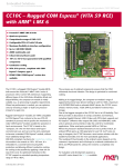
The CC10C is a Rugged COM Express® module (RCE) built around the
Freescale™ ARM® i.MX 6 series of processors with a Cortex®-A9 architecture.
Supporting different types of the i.MX 6Solo, 6DualLite, 6Dual and 6Quad
families, the computer-on-module is widely scalable, e.g., to processing or graphics
requirements. Where less performance is needed, you can optimize costs by
choosing a single- or dual-core processor instead of a quad core.
Rugged COM Express® modules are 100% compatible to COM Express® but
conform to the new VITA 59 standard (in process) which specifies the mechanics to
make COM Express® modules suitable for operation in harsh environments. The
CC10C is based on the "Compact", 95 x 95 mm form factor and Type 6 connector
pin-out, and can even be semi-customized to become a standard COM Express®
module, without much additional design effort.
With RCE-compliant mechanics for conduction cooling, the module's size extends
to 105 x 105 mm. It is embedded in a covered frame ensuring EMC protection and
allowing efficient conductive cooling. Air cooling is also possible by applying a
heat sink on top of the cover. Its optimized mechanics let the CC10C support an
extended operating temperature range of -40 to +85°C.
The exclusive use of soldered components ensures that the COM withstands shock
and vibration. The design is optimized for conformal coating.
Adding to its rugged design, the computer-on-module's range of supported
functions leave almost nothing to wish for. With a maximum of 4 GB DDR3 RAM
and an onboard eMMC device, the CC10C covers all basic memory needs. 3-Gbit
SATA is provided for external mass storage.
One of the biggest strengths of the CC10C lies in its I/O flexibility. The i.MX 6
provides an abundance of onchip controllers and interfaces, including Gigabit
Ethernet, USB 2.0 (also with OTG/client support) and PCI Express®. Different
video outputs like LVDS and HDMI/DVI, audio and an optional camera interface
make the card fit for multimedia applications. Other serial ports provide UARTs or
CAN bus.
Where the processor's standard functions are not a perfect match, an onboard FPGA
opens up 140 signal pins for user I/O. As IP cores are easy to integrate, the CC10C
becomes a semi-custom solution with the suitable functionality even for more
specialized applications.
The resulting I/O functionality in the ordered version depends on the customer's
requirements and will always be a tailored combination of i.MX 6 and FPGA-based
I/O, without the need for a completely new design.
For evaluation and development purposes a microATX carrier board, the XC15, is
available.
For more information see the XC15 carrier board data sheet.
MEN Mikro Elektronik GmbH
20CC10C00 E1 – 2014-12-05
2
Diagram
Diagram
DDR3 SDRAM
Boot
Flash
SATA (3 Gb)
GPIO/Control
SDIO/SDHC
eMMC Card
I2C
SDHC
SPI
Dual‐channel LVDS
UARTs
Freescale™
ARM® i.MX 6 Series
Processor
HDMI/DVI
MIPI CSI‐2
CAN bus
AC‘97 audio
ExpressCard
I2S audio
PWM
USB 2.0 (1 OTG)
PCIe x1
USB 2.0
Swidge
Altera® Cyclone® IV
FPGA
PHY
Gigabit Ethernet
PHY
Fast Ethernet
140 user I/Os
PCIe x1
(1.1)
COM Express® Type 6 connectors A‐B & C‐D
B Onboard
Options
MEN Mikro Elektronik GmbH
20CC10C00 E1 – 2014-12-05
B
3
Technical Data
Technical Data
CPU
• Freescale™ ARM® i.MX 6 Series (ARM® Cortex®-A9 architecture)
• The following CPU types are available:
- i.MX6S (i.MX 6Solo family)
- i.MX6DL (i.MX 6DualLite family)
- i.MX6D (i.MX 6Dual family)
- i.MX6Q (i.MX 6Quad family)
See Table 1, Processor core options on CC10C, on page 24 for processor options
and a feature matrix of the i.MX 6 series.
Memory
• System Memory
- Soldered DDR3
- 1 GB, 2 GB, or 4 GB
• Boot Flash
- 4 MB, 8 MB, or 16 MB
Mass Storage
• The following mass storage devices can be assembled:
- eMMC device, soldered; different sizes available
Graphics
• Integrated in i.MX 6 processor
• Multi-stream-capable HD video engine delivering up to 1080p60 decode,
1080p30 encode and 3D video playback in HD
• Maximum resolution: 1920 x 1200 pixels (WUXGA)
• Superior 3D graphics performance with up to four shaders performing 200 Mt/s
and OpenCL™ support
• Separate 2D and/or OpenVG Vertex acceleration engines for optimal user
interface experience
• Stereoscopic image sensor support for 3D imaging
Onboard Interfaces
• Available via COM Express® connectors
• Video
- One HDMI/DVI interface
- One LVDS interface, dual-channel
- One MIPI CSI-2 camera serial host interface; optional
• Audio
- One AC'97 audio interface
- One I2S audio interface
MEN Mikro Elektronik GmbH
20CC10C00 E1 – 2014-12-05
4
Technical Data
• SATA
- One channel, SATA Revision 2.x (3 Gbit/s); only with i.MX6D or i.MX6Q
• SDIO/SDHC
- One channel for MMC/SD/SDIO cards
• USB
- Two host channels, USB 2.0 (480 Mbit/s), or
- Six host channels, USB 2.0 (480 Mbit/s)
- One channel always implemented as OTG (On-The-Go) host/client port
• Ethernet
- One channel, 1000BASE-T (1 Gbit/s)
- One channel, 100BASE-T (100 Mbit/s); optional
- Two link and activity LED signals per channel
• PCI Express
- One x1 link (250 MB/s per link), PCIe® 1.1 (2.5 Gbit/s per lane)
• ExpressCard
- One interface
• CAN bus
- Two CAN bus channels, 2.0B CAN protocol, 1 Mbit/s
- Two additional CAN bus channels, 2.0A/B CAN protocol, 1 Mbit/s; with
FPGA; optional
- External transceivers to be implemented on carrier board
• UART
- Up to six interfaces, up to 4 Mbit/s
- Physical interfaces RS232 or RS422/RS485 depending on interface controller
and implementation on carrier board
• PWM
- Three PWM interfaces
• I2C
- Up to four I2C interfaces
• SPI
- Up to three SPI interfaces
• COM Express® control signals
- Four COM Express® control signals
• GPIO
- 9 GPIO lines, 4 GPO lines, 3 GPI lines
- 64 GPIO lines; with FPGA; optional
See Chapter 2.6 Customization Capabilities on page 26 for an overview of
configurable I/O functions.
MEN Mikro Elektronik GmbH
20CC10C00 E1 – 2014-12-05
5
Technical Data
FPGA
• No FPGA assembled, with custom configuration of i.MX 6 I/O interfaces, or
• FPGA Altera® Cyclone® IV, with custom IP core and i.MX 6 I/O configuration
- Total available pin count: 140 pins on COM Express® connectors
The IP cores that make sense and/or can be implemented depend on
the board model, available pin counts and number of logic elements.
Please contact MEN for information on feasibility.
Supervision and Control
• Power supervision and watchdog
• Temperature measurement
- i.MX 6 temperature measurement
- Additional onboard temperature sensor; optional
• Real-time clock, with supercapacitor or battery backup on the carrier board
Computer-On-Module Standard
• CC10C: VITA 59 RCE: Rugged COM Express® in process
- With conduction cooling cover and frame
- Rugged COM Express® Compact, Module Pin-out Type 6
• CC10: PICMG COM.0 COM Express® Module Base Specification
- COM Express® Compact, Module Pin-out Type 6
Electrical Specifications
• Supply voltage
- +12 V (9 to 16 V)
• Power consumption
- 12 W, measured in stress test using 15CC10C00, i.MX6Q quad-core @ 1.0
GHz
- 7.4 W, measured in test (activity on Gb Ethernet and 1 USB interface) using
15CC10C00, i.MX6Q quad-core @ 1.0 GHz
- 5 W, measured in test (activity on Gb Ethernet and 1 USB interface) using
15CC10-00, i.MX6S single-core @ 800 MHz
Mechanical Specifications
• Dimensions
- CC10C: 105 mm x 105 mm x 18 mm (conforming to VITA 59 RCE Compact
format, PCB mounted between a cover and a frame)
- CC10: 95 mm x 95 mm (conforming to PICMG COM.0 COM Express®
Compact format)
• Weight
- CC10C: 356 g (model 15CC10C00)
- CC10: 40 g (model 15CC10-00)
MEN Mikro Elektronik GmbH
20CC10C00 E1 – 2014-12-05
6
Technical Data
Environmental Specifications
• Temperature range (operation)
- -40°C to +85°C Tcase (VITA 59 cover/frame) (qualified components) (model
15CC10C00)
- -40°C to +85°C (qualified components) (model 15CC10-00)
• Temperature range (storage): -40°C to +85°C
• Cooling concept
- CC10C: Conduction-cooled according to VITA 59 RCE: Rugged COM
Express® in process, PCB with conduction cooling wings, mounted between
a cover and a frame
- CC10: Air-cooled according to PICMG COM.0 COM Express® standard
• Relative humidity (operation): max. 95% non-condensing
• Relative humidity (storage): max. 95% non-condensing
• Altitude: -300 m to +3000 m
• Shock: 50 m/s², 30 ms (EN 61373)
• Vibration (function): 1 m/s², 5 Hz to 150 Hz (EN 61373)
• Vibration (lifetime): 7.9 m/s², 5 Hz to 150 Hz (EN 61373)
• Conformal coating; optional
Reliability
• MTBF
- 652 986 h @ 40°C according to IEC/TR 62380 (RDF 2000)
(model 15CC10C00)
- 1 233 470 h @ 40°C according to IEC/TR 62380 (RDF 2000)
(model 15CC10-00)
Safety
• Flammability
- UL 94V-0
EMC
• EMC behavior generally depends on the system and housing surrounding the
COM module.
• The Rugged COM Express® module in its cover and frame supports the system
to meet the requirements of
- EN 55022 (radio disturbance)
- IEC 61000-4-2 (ESD)
- IEC 61000-4-3 (electromagnetic field immunity)
- IEC 61000-4-4 (burst)
- IEC 61000-4-5 (surge)
- IEC 61000-4-6 (conducted disturbances)
MEN Mikro Elektronik GmbH
20CC10C00 E1 – 2014-12-05
7
Technical Data
Software Support
• Linux
• VxWorks®
For more information on supported operating system versions and
drivers, please see the online data sheet.
BIOS
• U-Boot Universal Boot Loader
For available standard configurations see the online data sheet.
MEN Mikro Elektronik GmbH
20CC10C00 E1 – 2014-12-05
8
Product Safety
Product Safety
Electrostatic Discharge (ESD)
!
MEN Mikro Elektronik GmbH
20CC10C00 E1 – 2014-12-05
Computer boards and components contain electrostatic sensitive
devices. Electrostatic discharge (ESD) can damage components. To
protect the board and other components against damage from static
electricity, you should follow some precautions whenever you work on
your computer.
• Power down and unplug your computer system when working on the
inside.
• Hold components by the edges and try not to touch the IC chips,
leads, or circuitry.
• Use a grounded wrist strap before handling computer components.
• Place components on a grounded antistatic pad or on the bag that
came with the component whenever the components are separated
from the system.
• Only store the board in its original ESD-protected packaging. Retain
the original packaging in case you need to return the board to MEN
for repair.
9
About this Document
About this Document
This user manual is intended only for system developers and integrators, it is not
intended for end users.
It describes the hardware functions of the board, connection of peripheral devices
and integration into a system. It also provides additional information for special
applications and configurations of the board.
The manual does not include detailed information on individual components (data
sheets etc.). A list of literature is given in the appendix.
Product Naming
’CC10C’ is used throughout this document to name the products described.
However, descriptions are generally valid for the CC10 COM Express module, too.
Specific differences will be mentioned explicitly.
History
Issue
E1
MEN Mikro Elektronik GmbH
20CC10C00 E1 – 2014-12-05
Comments
First issue
Date
2014-12-05
10
About this Document
Conventions
!
Indicates important information or warnings concerning proper
functionality of the product described in this document.
The globe icon indicates a hyperlink that links directly to the Internet,
where the latest updated information is available.
When no globe icon is present, the hyperlink links to specific elements
and information within this document.
italics
Folder, file and function names are printed in italics.
bold
Bold type is used for emphasis.
mono
A monospaced font type is used for hexadecimal numbers, listings, C
function descriptions or wherever appropriate. Hexadecimal numbers
are preceded by "0x".
comment
Comments embedded into coding examples are shown in green text.
IRQ#
/IRQ
Signal names followed by a hashtag "#" or preceded by a forward
slash "/" indicate that this signal is either active low or that it becomes
active at a falling edge.
in/out
Signal directions in signal mnemonics tables generally refer to the
corresponding board or component, "in" meaning "to the board or
component", "out" meaning "from it the board or component".
Blue vertical lines in the outer margin indicate sections where changes
have been made to this version of the document.
MEN Mikro Elektronik GmbH
20CC10C00 E1 – 2014-12-05
11
About this Document
Legal Information
Changes
MEN Mikro Elektronik GmbH ("MEN") reserves the right to make changes without further notice to any products
herein.
Warranty, Guarantee, Liability
MEN makes no warranty, representation or guarantee of any kind regarding the suitability of its products for any
particular purpose, nor does MEN assume any liability arising out of the application or use of any product or
circuit, and specifically disclaims any and all liability, including, without limitation, consequential or incidental
damages. TO THE EXTENT APPLICABLE, SPECIFICALLY EXCLUDED ARE ANY IMPLIED
WARRANTIES ARISING BY OPERATION OF LAW, CUSTOM OR USAGE, INCLUDING WITHOUT
LIMITATION, THE IMPLIED WARRANTIES OF MERCHANTABILITY AND FITNESS FOR A
PARTICULAR PURPOSE OR USE. In no event shall MEN be liable for more than the contract price for the
products in question. If buyer does not notify MEN in writing within the foregoing warranty period, MEN shall
have no liability or obligation to buyer hereunder.
The publication is provided on the terms and understanding that:
1. MEN is not responsible for the results of any actions taken on the basis of information in the publication, nor
for any error in or omission from the publication; and
2. MEN is not engaged in rendering technical or other advice or services.
MEN expressly disclaims all and any liability and responsibility to any person, whether a reader of the publication
or not, in respect of anything, and of the consequences of anything, done or omitted to be done by any such person
in reliance, whether wholly or partially, on the whole or any part of the contents of the publication.
Conditions for Use, Field of Application
The correct function of MEN products in mission-critical and life-critical applications is limited to the
environmental specification given for each product in the technical user manual. The correct function of MEN
products under extended environmental conditions is limited to the individual requirement specification and
subsequent validation documents for each product for the applicable use case and has to be agreed upon in writing
by MEN and the customer. Should the customer purchase or use MEN products for any unintended or
unauthorized application, the customer shall indemnify and hold MEN and its officers, employees, subsidiaries,
affiliates, and distributors harmless against all claims, costs, damages, and expenses, and reasonable attorney fees
arising out of, directly or indirectly, any claim or personal injury or death associated with such unintended or
unauthorized use, even if such claim alleges that MEN was negligent regarding the design or manufacture of the
part. In no case is MEN liable for the correct function of the technical installation where MEN products are a part
of.
Trademarks
All products or services mentioned in this publication are identified by the trademarks, service marks, or product
names as designated by the companies which market those products. The trademarks and registered trademarks
are held by the companies producing them. Inquiries concerning such trademarks should be made directly to those
companies.
Conformity
MEN products are no ready-made products for end users. They are tested according to the standards given in the
Technical Data and thus enable you to achieve certification of the product according to the standards applicable in
your field of application.
MEN Mikro Elektronik GmbH
20CC10C00 E1 – 2014-12-05
12
About this Document
RoHS
Since July 1, 2006 all MEN standard products comply with RoHS legislation.
Since January 2005 the SMD and manual soldering processes at MEN have already been completely lead-free.
Between June 2004 and June 30, 2006 MEN’s selected component suppliers have changed delivery to RoHScompliant parts. During this period any change and status was traceable through the MEN ERP system and the
boards gradually became RoHS-compliant.
WEEE Application
The WEEE directive does not apply to fixed industrial plants and tools. The compliance is the responsibility of the
company which puts the product on the market, as defined in the directive; components and sub-assemblies are
not subject to product compliance.
In other words: Since MEN does not deliver ready-made products to end users, the WEEE directive is not
applicable for MEN. Users are nevertheless recommended to properly recycle all electronic boards which have
passed their life cycle.
Nevertheless, MEN is registered as a manufacturer in Germany. The registration number can be provided on
request.
Copyright © 2014 MEN Mikro Elektronik GmbH. All rights reserved.
Germany
MEN Mikro Elektronik GmbH
Neuwieder Straße 3-7
90411 Nuremberg
Phone +49-911-99 33 5-0
Fax +49-911-99 33 5-901
E-mail [email protected]
www.men.de
MEN Mikro Elektronik GmbH
20CC10C00 E1 – 2014-12-05
France
MEN Mikro Elektronik SAS
18, rue René Cassin
ZA de la Châtelaine
74240 Gaillard
Phone +33 (0) 450-955-312
Fax +33 (0) 450-955-211
E-mail [email protected]
www.men-france.fr
USA
MEN Micro Inc.
860 Penllyn Blue Bell Pike
Blue Bell, PA 19422
Phone (215) 542-9575
Fax (215) 542-9577
E-mail [email protected]
www.menmicro.com
13
Contents
Contents
1 Getting Started . . . . . . . . . . . . . . . . . . . . . . . . . . . . . . . . . . . . . . . . . . . . . . . .
1.1 Map of the Board. . . . . . . . . . . . . . . . . . . . . . . . . . . . . . . . . . . . . . . . .
1.1.1
CC10C Rugged COM Express . . . . . . . . . . . . . . . . . . . . . . .
1.1.2
CC10 COM Express . . . . . . . . . . . . . . . . . . . . . . . . . . . . . . .
1.2 First Operation. . . . . . . . . . . . . . . . . . . . . . . . . . . . . . . . . . . . . . . . . . .
1.3 Installing Operating System Software. . . . . . . . . . . . . . . . . . . . . . . . .
1.4 Installing Driver Software . . . . . . . . . . . . . . . . . . . . . . . . . . . . . . . . . .
18
18
18
19
20
21
21
2 Functional Description . . . . . . . . . . . . . . . . . . . . . . . . . . . . . . . . . . . . . . . . . .
2.1 Power Supply and Control. . . . . . . . . . . . . . . . . . . . . . . . . . . . . . . . . .
2.2 Board Supervision and Management. . . . . . . . . . . . . . . . . . . . . . . . . .
2.2.1
Temperature and Voltage. . . . . . . . . . . . . . . . . . . . . . . . . . . .
2.2.2
Watchdog. . . . . . . . . . . . . . . . . . . . . . . . . . . . . . . . . . . . . . . .
2.3 Reset . . . . . . . . . . . . . . . . . . . . . . . . . . . . . . . . . . . . . . . . . . . . . . . . . .
2.4 Real-Time Clock (RTC) . . . . . . . . . . . . . . . . . . . . . . . . . . . . . . . . . . .
2.5 Processor Core. . . . . . . . . . . . . . . . . . . . . . . . . . . . . . . . . . . . . . . . . . .
2.5.1
Thermal Considerations . . . . . . . . . . . . . . . . . . . . . . . . . . . .
2.6 Customization Capabilities . . . . . . . . . . . . . . . . . . . . . . . . . . . . . . . . .
2.6.1
FPGA I/O . . . . . . . . . . . . . . . . . . . . . . . . . . . . . . . . . . . . . . .
2.6.2
ARM i.MX 6 I/O. . . . . . . . . . . . . . . . . . . . . . . . . . . . . . . . . .
2.6.3
Interface Configurability Overview . . . . . . . . . . . . . . . . . . .
2.7 Memory . . . . . . . . . . . . . . . . . . . . . . . . . . . . . . . . . . . . . . . . . . . . . . . .
2.7.1
DRAM System Memory . . . . . . . . . . . . . . . . . . . . . . . . . . . .
2.7.2
Boot Flash . . . . . . . . . . . . . . . . . . . . . . . . . . . . . . . . . . . . . . .
2.8 Mass Storage . . . . . . . . . . . . . . . . . . . . . . . . . . . . . . . . . . . . . . . . . . . .
2.8.1
Serial ATA (SATA) . . . . . . . . . . . . . . . . . . . . . . . . . . . . . . . .
2.8.2
eMMC Multimedia Card (SDHC Interface) . . . . . . . . . . . . .
2.8.3
SDIO/SDHC Interface . . . . . . . . . . . . . . . . . . . . . . . . . . . . .
2.9 Multimedia . . . . . . . . . . . . . . . . . . . . . . . . . . . . . . . . . . . . . . . . . . . . .
2.9.1
Video . . . . . . . . . . . . . . . . . . . . . . . . . . . . . . . . . . . . . . . . . . .
2.9.2
Audio. . . . . . . . . . . . . . . . . . . . . . . . . . . . . . . . . . . . . . . . . . .
2.10 USB . . . . . . . . . . . . . . . . . . . . . . . . . . . . . . . . . . . . . . . . . . . . . . . . . . .
2.11 Ethernet . . . . . . . . . . . . . . . . . . . . . . . . . . . . . . . . . . . . . . . . . . . . . . . .
2.11.1 Ethernet MAC Addresses . . . . . . . . . . . . . . . . . . . . . . . . . . .
2.11.2 Ethernet Status LEDs . . . . . . . . . . . . . . . . . . . . . . . . . . . . . .
2.12 PCI Express . . . . . . . . . . . . . . . . . . . . . . . . . . . . . . . . . . . . . . . . . . . . .
2.13 ExpressCard Interface . . . . . . . . . . . . . . . . . . . . . . . . . . . . . . . . . . . . .
2.14 CAN Bus . . . . . . . . . . . . . . . . . . . . . . . . . . . . . . . . . . . . . . . . . . . . . . .
2.15 UART Interfaces . . . . . . . . . . . . . . . . . . . . . . . . . . . . . . . . . . . . . . . . .
2.16 PWM . . . . . . . . . . . . . . . . . . . . . . . . . . . . . . . . . . . . . . . . . . . . . . . . . .
2.17 I2C . . . . . . . . . . . . . . . . . . . . . . . . . . . . . . . . . . . . . . . . . . . . . . . . . . . .
2.17.1 I2C Interfaces Controlled by i.MX 6 . . . . . . . . . . . . . . . . . .
2.17.2 I2C Interfaces Controlled by Onboard FPGA. . . . . . . . . . . .
22
22
22
22
22
23
23
24
25
26
26
26
27
30
30
30
30
30
30
31
31
31
33
33
34
34
35
35
35
36
37
38
38
38
39
MEN Mikro Elektronik GmbH
20CC10C00 E1 – 2014-12-05
14
Contents
2.18 SPI . . . . . . . . . . . . . . . . . . . . . . . . . . . . . . . . . . . . . . . . . . . . . . . . . . . .
2.19 GPIO . . . . . . . . . . . . . . . . . . . . . . . . . . . . . . . . . . . . . . . . . . . . . . . . . .
2.19.1 GPIO Lines Controlled by i.MX 6 . . . . . . . . . . . . . . . . . . . .
2.19.2 GPIO Lines Controlled by Onboard FPGA . . . . . . . . . . . . .
2.20 Rugged COM Express (VITA 59) . . . . . . . . . . . . . . . . . . . . . . . . . . . .
2.20.1 Module Form Factors . . . . . . . . . . . . . . . . . . . . . . . . . . . . . .
2.20.2 Thermal Concept. . . . . . . . . . . . . . . . . . . . . . . . . . . . . . . . . .
2.20.3 COM Express Connectors. . . . . . . . . . . . . . . . . . . . . . . . . . .
2.20.4 COM Express Control Signals . . . . . . . . . . . . . . . . . . . . . . .
39
40
40
40
41
41
41
43
55
3 U-Boot Boot Loader . . . . . . . . . . . . . . . . . . . . . . . . . . . . . . . . . . . . . . . . . . . .
3.1 General . . . . . . . . . . . . . . . . . . . . . . . . . . . . . . . . . . . . . . . . . . . . . . . .
3.2 Getting Started: Setting Up Your Operating System . . . . . . . . . . . . . .
3.2.1
Setting Up the Boot File . . . . . . . . . . . . . . . . . . . . . . . . . . . .
3.2.2
Setting Up the Boot and TFTP Parameters . . . . . . . . . . . . . .
3.2.3
Starting Up the Operating System . . . . . . . . . . . . . . . . . . . .
3.3 Interacting with U-Boot. . . . . . . . . . . . . . . . . . . . . . . . . . . . . . . . . . . .
3.3.1
Setting Up a Console Connection . . . . . . . . . . . . . . . . . . . . .
3.3.2
Entering the U-Boot Command Line . . . . . . . . . . . . . . . . . .
3.3.3
User Interface Basics. . . . . . . . . . . . . . . . . . . . . . . . . . . . . . .
3.4 U-Boot Images and Start-Up . . . . . . . . . . . . . . . . . . . . . . . . . . . . . . . .
3.4.1
Images . . . . . . . . . . . . . . . . . . . . . . . . . . . . . . . . . . . . . . . . . .
3.4.2
Booting an Operating System . . . . . . . . . . . . . . . . . . . . . . . .
3.5 Updating the Boot Flash . . . . . . . . . . . . . . . . . . . . . . . . . . . . . . . . . . .
3.5.1
Update via the Serial Console . . . . . . . . . . . . . . . . . . . . . . . .
3.5.2
Update via Network . . . . . . . . . . . . . . . . . . . . . . . . . . . . . . .
3.5.3
Update via USB . . . . . . . . . . . . . . . . . . . . . . . . . . . . . . . . . .
3.5.4
Performing an Update . . . . . . . . . . . . . . . . . . . . . . . . . . . . . .
3.5.5
Updating U-Boot Image 1. . . . . . . . . . . . . . . . . . . . . . . . . . .
3.6 Working with Interfaces and Devices . . . . . . . . . . . . . . . . . . . . . . . . .
3.6.1
PCI . . . . . . . . . . . . . . . . . . . . . . . . . . . . . . . . . . . . . . . . . . . .
3.6.2
USB . . . . . . . . . . . . . . . . . . . . . . . . . . . . . . . . . . . . . . . . . . . .
3.6.3
eMMC/SDHC . . . . . . . . . . . . . . . . . . . . . . . . . . . . . . . . . . . .
3.6.4
I2C. . . . . . . . . . . . . . . . . . . . . . . . . . . . . . . . . . . . . . . . . . . . .
3.6.5
PWM . . . . . . . . . . . . . . . . . . . . . . . . . . . . . . . . . . . . . . . . . . .
3.6.6
Watchdog. . . . . . . . . . . . . . . . . . . . . . . . . . . . . . . . . . . . . . . .
3.7 Diagnostic Tests. . . . . . . . . . . . . . . . . . . . . . . . . . . . . . . . . . . . . . . . . .
3.8 U-Boot Configuration and Organization . . . . . . . . . . . . . . . . . . . . . . .
3.8.1
Boot Flash Memory Map . . . . . . . . . . . . . . . . . . . . . . . . . . .
3.8.2
Environment Variables . . . . . . . . . . . . . . . . . . . . . . . . . . . . .
3.9 U-Boot Commands . . . . . . . . . . . . . . . . . . . . . . . . . . . . . . . . . . . . . . .
3.10 Hardware Interfaces Not Supported by U-Boot . . . . . . . . . . . . . . . . .
56
56
57
57
57
58
59
59
59
60
63
63
63
67
67
67
67
67
69
70
70
70
71
71
72
72
73
74
74
74
77
80
MEN Mikro Elektronik GmbH
20CC10C00 E1 – 2014-12-05
15
Contents
4 Organization of the Board . . . . . . . . . . . . . . . . . . . . . . . . . . . . . . . . . . . . . . .
4.1 Global Address Map . . . . . . . . . . . . . . . . . . . . . . . . . . . . . . . . . . . . . .
4.2 PCI Devices . . . . . . . . . . . . . . . . . . . . . . . . . . . . . . . . . . . . . . . . . . . . .
4.3 SMBus Devices . . . . . . . . . . . . . . . . . . . . . . . . . . . . . . . . . . . . . . . . . .
81
81
81
81
5 Appendix . . . . . . . . . . . . . . . . . . . . . . . . . . . . . . . . . . . . . . . . . . . . . . . . . . . . .
5.1 Literature and Web Resources . . . . . . . . . . . . . . . . . . . . . . . . . . . . . . .
5.1.1
COM Express . . . . . . . . . . . . . . . . . . . . . . . . . . . . . . . . . . . .
5.1.2
Rugged COM Express . . . . . . . . . . . . . . . . . . . . . . . . . . . . .
5.1.3
CPU . . . . . . . . . . . . . . . . . . . . . . . . . . . . . . . . . . . . . . . . . . . .
5.1.4
eMMC . . . . . . . . . . . . . . . . . . . . . . . . . . . . . . . . . . . . . . . . . .
5.1.5
SATA . . . . . . . . . . . . . . . . . . . . . . . . . . . . . . . . . . . . . . . . . . .
5.1.6
LVDS. . . . . . . . . . . . . . . . . . . . . . . . . . . . . . . . . . . . . . . . . . .
5.1.7
DVI . . . . . . . . . . . . . . . . . . . . . . . . . . . . . . . . . . . . . . . . . . . .
5.1.8
USB . . . . . . . . . . . . . . . . . . . . . . . . . . . . . . . . . . . . . . . . . . . .
5.1.9
Ethernet . . . . . . . . . . . . . . . . . . . . . . . . . . . . . . . . . . . . . . . . .
5.1.10 PCI Express. . . . . . . . . . . . . . . . . . . . . . . . . . . . . . . . . . . . . .
5.1.11 AC’97 Audio . . . . . . . . . . . . . . . . . . . . . . . . . . . . . . . . . . . . .
5.1.12 CAN Bus . . . . . . . . . . . . . . . . . . . . . . . . . . . . . . . . . . . . . . . .
5.1.13 I2C Bus . . . . . . . . . . . . . . . . . . . . . . . . . . . . . . . . . . . . . . . . .
5.2 Finding out the Product’s Article Number, Revision and Serial
Number . . . . . . . . . . . . . . . . . . . . . . . . . . . . . . . . . . . . . . . . . . . . . . . .
5.3 Dimensions of CC10C Rugged COM Express Compact Module. . . .
82
82
82
82
82
82
82
83
83
83
83
83
83
84
84
MEN Mikro Elektronik GmbH
20CC10C00 E1 – 2014-12-05
84
84
16
Figures
Figure 1. Map of the board (CC10C Rugged COM Express) . . . . . . . . . . . . . . .
Figure 2. Map of the board (CC10 COM Express) . . . . . . . . . . . . . . . . . . . . . . .
Figure 3. Rugged COM Express Compact module with cooling wings (PCB
without frame and cover) . . . . . . . . . . . . . . . . . . . . . . . . . . . . . . . . . . .
Figure 4. Labels giving the product’s article number, revision and serial
number . . . . . . . . . . . . . . . . . . . . . . . . . . . . . . . . . . . . . . . . . . . . . . . . .
18
19
42
84
Tables
Table 1.
Table 2.
Table 3.
Table 4.
Table 5.
Table 6.
Table 7.
Table 8.
Table 9.
Table 10.
Table 11.
Table 12.
Table 13.
Table 14.
Table 15.
Table 16.
Table 17.
Table 18.
MEN Mikro Elektronik GmbH
20CC10C00 E1 – 2014-12-05
Processor core options on CC10C . . . . . . . . . . . . . . . . . . . . . . . . . . . .
Interface configurability overview (COM Express connectors). . . . . .
Multiplexed interfaces for i.MX 6 or FPGA use . . . . . . . . . . . . . . . . .
Ethernet status LED modes . . . . . . . . . . . . . . . . . . . . . . . . . . . . . . . . .
UART interface control and configurability . . . . . . . . . . . . . . . . . . . .
Form factors defined for Rugged COM Express . . . . . . . . . . . . . . . . .
Pin assignment of COM Express connectors J1 and J2 – CC10C . . . .
Pin assignment of COM Express connectors J1 and J2 – CC10 . . . . .
Signal Mnemonics . . . . . . . . . . . . . . . . . . . . . . . . . . . . . . . . . . . . . . . .
U-Boot – Boot Flash memory map. . . . . . . . . . . . . . . . . . . . . . . . . . . .
U-Boot – Environment variables – OS boot. . . . . . . . . . . . . . . . . . . . .
U-Boot – Environment variables – Network . . . . . . . . . . . . . . . . . . . .
U-Boot – Environment variables – Console. . . . . . . . . . . . . . . . . . . . .
U-Boot – Environment variables – Other. . . . . . . . . . . . . . . . . . . . . . .
U-Boot – Command reference . . . . . . . . . . . . . . . . . . . . . . . . . . . . . . .
Global address map . . . . . . . . . . . . . . . . . . . . . . . . . . . . . . . . . . . . . . .
PCI devices . . . . . . . . . . . . . . . . . . . . . . . . . . . . . . . . . . . . . . . . . . . . . .
SMBus devices . . . . . . . . . . . . . . . . . . . . . . . . . . . . . . . . . . . . . . . . . . .
24
27
29
35
37
41
43
47
50
74
74
75
76
76
77
81
81
81
17
Getting Started
1
Getting Started
This chapter gives an overview of the board and some hints for first installation.
1.1
Map of the Board
1.1.1
CC10C Rugged COM Express
The following board map shows the board inside the cover and frame from its
connector side (bottom). The cover includes holes for mounting the Rugged COM
Express module onto a carrier.
If you want to use a Rugged COM Express (RCE) module together with a COM
Express carrier or other custom carrier board, please make sure that the carrier
provides appropriate ’landing zones’ for the RCE frame.
For the exact dimensions of CC10C, see Chapter 5.3 Dimensions of CC10C
Rugged COM Express Compact Module on page 84.
Figure 1. Map of the board (CC10C Rugged COM Express)
Cooling Wing
Revision
Cooling Wing
Cooling Wing
Serial
No.
D110
D1
C110
C1
COM Express Connectors
B110
B1
A110
A1
Cooling Wing
COM Express screw holes for installation on the carrier board.
Screws connecting the frame and cover of the module. Do not remove.
Holes for optional carrier board fixing when used as wall-mount assembly
For more information on Rugged COM Express mechanics see the VITA 59
specification: Chapter 5.1.2 Rugged COM Express on page 82.
MEN Mikro Elektronik GmbH
20CC10C00 E1 – 2014-12-05
18
Getting Started
1.1.2
CC10 COM Express
The following board map shows the COM.0 CC10 board from its connector side
(bottom).
For the dimensions of COM Express Compact modules, please see the COM
Express COM.0 specification. See Chapter 5.1.1 COM Express on page 82.
Figure 2. Map of the board (CC10 COM Express)
Revision
Serial
No.
D110
D1
C110
C1
COM Express Connectors
B110
B1
A110
A1
COM Express screw holes for installation on the carrier board.
MEN Mikro Elektronik GmbH
20CC10C00 E1 – 2014-12-05
19
Getting Started
1.2
First Operation
You can use the following check list when installing the board for the first time and
with minimum configuration using a Windows host PC.
The U-Boot firmware is preinstalled on the CC10C and is preconfigured for the
board.
Power down the system.
If you use a Rugged COM Express (RCE) module embedded into an aluminum
frame together with a COM Express carrier or other custom carrier board,
please make sure that the carrier provides appropriate ’landing zones’ for the
RCE frame.
For the exact dimensions of CC10C, see Chapter 5.3 Dimensions of CC10C
Rugged COM Express Compact Module on page 84.
Plug the CC10C on your carrier board, making sure that the COM Express connectors are properly aligned.
Fasten the four screws connecting the COM Express module to the carrier
(marked in red in Figure 1, Map of the board (CC10C Rugged COM Express)
on page 18 and Figure 2, Map of the board (CC10 COM Express) on page 19).
To provide a better example, we assume that you are using MEN’s standard
evaluation carrier, XC15, which provides the necessary connections for a Windows
host PC.
You can find more information on the XC15 in the XC15 User Manual,
which is available for download on MEN’s website.
Connect a Windows PC to the RS232 interface of XC15.
2
6
3
7
Ethernet
RJ45
1
2
3
Dual USB 2.0
Type A
USB 3.0
Type A
RS232
9‐Pin D‐Sub
DisplayPort
HD Audio
In/Out
Power-up the system.
Start up a terminal program on your Windows PC, e.g., HyperTerm, and open a
terminal connection.
Set your terminal connection to the following protocol:
MEN Mikro Elektronik GmbH
20CC10C00 E1 – 2014-12-05
115 200 baud data transmission rate
8 data bits
1 stop bit
No parity
20
Getting Started
U-Boot will load and then display a command line. The terminal displays a
message similar to the following:
U-Boot 2013.01 (Sep 10 2014 - 17:58:33) MEN CC10-Quad V0.4 (standard)
CPU:
Freescale i.MX6Q rev1.2 at 984 MHz
Reset cause: POR
Board: MEN CC10
I2C:
ready
RAM Configuration:
Bank #0: 10000000 2 GiB
WARNING: Caches not enabled
MMC:
FSL_SDHC: 0, FSL_SDHC: 1
SF: Detected N25Q032 with page size 64 KiB, total 4 MiB
auto-detected panel HDMI
enable_hdmi: setup HDMI monitor
Display: HDMI (1024x768)
In:
serial
Out:
serial
Err:
serial
Thermal fuse is 0x59e4ec7d, raw_25c=1438 raw_hot=1260 hot_temp=125 C scale=0.56
Temperature raw=1378 temperature= 58.70 C
Net:
using phy at Nr.3, phy_id=0x221622
FEC [PRIME]
=>
Now you can make configurations for your operating system in the U-Boot
boot loader.
See the detailed description in Chapter 3 U-Boot Boot Loader on page 56.
1.3
Installing Operating System Software
The board supports Linux and VxWorks.
!
By default, no operating system is installed on the board. Please refer
to the respective manufacturer's documentation on how to configure
your operating system image!
•
•
1.4
You can find any BSP software available on the CC10C pages on
MEN’s website.
The U-Boot Chapter of this manual describes the first steps of how
to get your operating system running, see Chapter 3.2 Getting
Started: Setting Up Your Operating System on page 57.
Installing Driver Software
For a detailed description on how to install driver software please refer to the
respective documentation of the software package to be installed.
You can find any driver software available for download on the CC10C
pages on MEN’s website.
MEN Mikro Elektronik GmbH
20CC10C00 E1 – 2014-12-05
21
Functional Description
2
Functional Description
The following describes the individual functions of the board and their
configuration on the board. There is no detailed description of the individual
controller chips and the CPU. They can be obtained from the data sheets or data
books of the semiconductor manufacturer concerned.
See Chapter 5.1 Literature and Web Resources on page 82.
Please note: The board BSPs for the different operating systems may
not support all the functions of the CC10C. For more information on
hardware support please see the respective BSP data sheet on MEN’s
website.
2.1
Power Supply and Control
The CC10C board is supplied with +12 V (9 to 16 V) only via COM Express
connectors J1/J2. All other required voltages are generated on the board.
The CC10C supports the PWR_OK signal (input from main power supply) available
at the COM Express connector according to the PICMG COM.0 standard.
The CC10C supports the i.MX 6 processors’ power down modes to reduce power
consumption.
2.2
Board Supervision and Management
2.2.1
Temperature and Voltage
The board supports temperature measurement and voltage monitoring as integrated
in the i.MX 6 processor.
A voltage monitor supervises all onboard core voltages and holds the CPU in reset
condition until the supply voltage is within its nominal values.
As an option, the board is also available with an additional onboard temperature
sensor.
2.2.2
Watchdog
The CC10C supports the watchdog integrated in the i.MX 6 processor.
The watchdog can be enabled or disabled and can be triggered by a software
application. This function is supported by the CC10C board support packages.
The watchdog provides timeout periods from 0.5 to 128 seconds with a time
resolution of 0.5 seconds.
MEN Mikro Elektronik GmbH
20CC10C00 E1 – 2014-12-05
22
Functional Description
2.3
Reset
The CC10C provides the reset signals CB_RESET# (carrier board reset) and
SYS_RESET# (reset button input) which are available at the COM Express
connector according to the PICMG COM.0 standard.
You can find the pinout for the reset signals in Chapter 2.20.3 COM Express
Connectors on page 43.
2.4
Real-Time Clock (RTC)
The board includes a real-time clock inside the i.MX 6 processor. For data retention
during power off the RTC can be backed up by a supercapacitor or battery installed
on the carrier.
For back-up voltage supply from the carrier board, the board supports a 3 V input
using J1 pin VCC_RTC (J1-A47).
Also see pinout in Chapter 2.20.3 COM Express Connectors on page 43.
You can set the system date and time through the U-Boot firmware.
MEN Mikro Elektronik GmbH
20CC10C00 E1 – 2014-12-05
23
Functional Description
2.5
Processor Core
The computer-on-module is built around Freescale’s i.MX 6 scalable multicore
platform, which includes single-, dual- and quad-core families based on the ARM
Cortex-A9 architecture. The i.MX 6 series combines the power-efficient processing
capabilities of ARM Cortex-A9 with 3D and 2D graphics as well as high-definition
video, providing multimedia performance next to serial connectivity.
Table 1. Processor core options on CC10C
Family
Cores
Core
L2 Cache
Frequency
DDR3 Width
and Clock
Video
SATA
i.MX6S
(Solo)
1
800 MHz or 512 KB
1.0 GHz
32 bits, 400 MHz 3D graphics with one
shader, 2D graphics
engine, two MIPI CSI-2
data lanes
-
i.MX6DL
(DualLite)
2
800 MHz or 512 KB
1.0 GHz
64 bits, 400 MHz 3D graphics with one
shader, 2D graphics
engine, two MIPI CSI-2
data lanes
-
i.MX6D
(Dual)
2
850 MHz or 1 MB
1.0 GHz
64 bits, 533 MHz 3D graphics with four
shaders, two 2D graphics
engines, four MIPI CSI-2
data lanes
3 Gbit/s
i.MX6Q
(Quad)
4
850 MHz or 1 MB
1.0 GHz
64 bits, 533 MHz 3D graphics with four
shaders, two 2D graphics
engines, four MIPI CSI-2
data lanes
3 Gbit/s
Further options such as higher core frequencies are available on request, using
processors from Freescale’s "Consumer" category. However, these processors do not
support extended operating temperature ranges.
The processor families above support -40 to +85°C.
The CC10C supports the i.MX 6 processors’ power down modes to reduce power
consumption.
MEN Mikro Elektronik GmbH
20CC10C00 E1 – 2014-12-05
24
Functional Description
2.5.1
Thermal Considerations
The power dissipation of CC10C heavily depends on its processor and I/O
configuration and on the workload.
As measured during a stress test (e.g., with busy Ethernet and graphics functions),
the CC10C generates a typical 12 W of power dissipation with an i.MX6Q quadcore processor operated at 1.0 GHz.
If stripped down to a single-core processor and with lower I/O load, the COM’s
power dissipation reduces to approx. 5 W, as measured in a test with activity on the
Gigabit Ethernet interface and on one USB interface.
Rugged COM Express modules (VITA 59) are enclosed inside a cover and frame
and therefore provides a flexible thermal interface that can be used as needed to
fulfill the thermal needs of the application. Typically you should use it for
conduction cooling or convection cooling. It depends on the system configuration
and airflow if an additional heat sink is needed or not. In any case you should check
your thermal conditions and implement appropriate cooling.
See also Chapter 2.20.2 Thermal Concept on page 41.
!
Please note that if you do not use the cover and frame supplied by
MEN and/or no heat sink, warranty on functionality and reliability of
the CC10C may cease. If you have any questions or problems
regarding thermal behavior, please contact MEN.
COM Express modules (COM.0) may also need additional cooling facilities,
depending on the configuration of the board and the general system design, i.e.
integration of the computer-on-module into the system. Implementation is up to the
customer.
A general heat spreader solution, e.g., for evaluation purposes, is available from
MEN as an accessory for CC10 (part number 05CC10-00).
See the CC10C pages on MEN’s website for ordering information.
MEN Mikro Elektronik GmbH
20CC10C00 E1 – 2014-12-05
25
Functional Description
2.6
Customization Capabilities
The CC10C has the capability of implementing all kinds of storage and I/O
functions on a wide scale. Two main components control I/O on the board:
• ARM i.MX 6 processor
• Onboard FPGA
The signals are available at the COM Express connector. Many pins are multiplexed
to be driven by either i.MX 6 or FPGA signals.
For an overview of signals multiplexed to use either i.MX 6 or FPGA I/O, see
Chapter 2.6.3.1 Multiplexed Interfaces for i.MX 6 or FPGA I/O on page 29.
MEN offers different configurations with and without FPGA as standard versions.
Depending on your I/O needs, MEN can provide a semi-custom version of the board
with the functions desired.
While the CC10C is extremely flexible in its I/O configuration, line routing is also
complex and not all combinations are possible. The configuration of the available
standard versions of the COM reflect both the i.MX 6 and FPGA capabilities, as can
be seen in the standard COM Express connector pinouts.
You can find the pinouts for different standard board versions, with and without an
FPGA, in Chapter 2.20.3 COM Express Connectors on page 43.
2.6.1
FPGA I/O
With an Altera Cyclone IV FPGA assembled, the CC10C provides 140 FPGAcontrolled I/O pins. While some interfaces are implemented by standard with an
FPGA assembled, IP cores with the desired functionality are integrated as needed
for all free pins.
The CC10C FPGA can be updated in the field. This is supported by the available
BSPs and by a software tool for FPGA Flash updates provided by MEN.
You can find any BSP and driver software available for download on
the CC10C pages on MEN’s website.
You can find the pinout of FPGA-controlled signals in Table 7, Pin assignment of
COM Express connectors J1 and J2 – CC10C on page 43.
More information on FPGA technology and usable IP cores is available
on the MEN website in the "User I/O in FPGA" section.
2.6.2
ARM i.MX 6 I/O
Since the i.MX 6 series of processors come with an abundance of I/O functions, no
FPGA may be needed for many applications.
MEN Mikro Elektronik GmbH
20CC10C00 E1 – 2014-12-05
26
Functional Description
2.6.3
Interface Configurability Overview
This chapter gives an overview of the board’s interface options. In any case we
recommend that you contact our sales team for semi-custom configuration of
CC10C for your requirements.
Contact MEN’s sales team for further information.
The following table relates to the pinout of the COM Express connectors. It gives an
interface list to show what is configurable on the board.
It does not give a full list of options of the board. E.g., assembly of an eMMC is a
storage option, but eMMC signals are not relevant for the connector pinout.
Please see Table 1, Processor core options on CC10C, on page 24 for a feature
matrix of the i.MX 6 series.
Table 2. Interface configurability overview (COM Express connectors)
Function
Configurability
i.MX 6
I/O
FPGA
I/O
Configurable
Standard
CC10C (RCE
VITA 59)
Configuration
Standard
CC10 (COM.0)
Configuration
x
1
-
Comment
Storage
SATA
1 interface
x
SDIO/SDHC
1 interface
x
1
1
LVDS
1 dualchannel
interface
x
1
1
HDMI/DVI
1 interface
x
1
1
MIPI CSI-2
camera
1 interface, 2
or 4 data
lanes
x
-
1
(2 data lanes)
AC'97 audio
1 interface
x
1
1
I2S audio
1 interface
x
1
1
USB 2.0
2 or 6
interfaces
x
6
2
Ethernet
1 interface,
1000BASE-T
x
1
1
1
-
Depends on i.MX 6
processor type
Multimedia
x
Data lanes depend on
i.MX 6 processor type
I/O
1 interface,
100BASE-T
x
x
x
PCI Express
1.1
1 x1 link
x
1
1
ExpressCard
1 interface
x
1
1
MEN Mikro Elektronik GmbH
20CC10C00 E1 – 2014-12-05
Dedicated FPGA I/O,
with Ethernet PHY (in
addition to 140
configurable pins)
27
Functional Description
Function
UARTs
Configurability
i.MX 6
I/O
Up to 4
interfaces
with different
handshake
configuration
x
Up to 4
interfaces
with different
handshake
configuration
CAN bus
2 channels
2.0B CAN
protocol
x
9 GPIOs,
4 GPOs,
3 GPIs
x
x
PWM
3 interfaces
x
I2C
2 interfaces
x
2 interfaces
x
2 (without
handshake
lines)
4 (2 with
handshake
lines)
x
4 (with
handshake
lines)
-
2
2
2
-
9 GPIOs,
4 GPOs,
3 GPIs
9 GPIOs,
4 GPOs,
3 GPIs
64
-
More lines possible with
custom FPGA
configuration
3
3
A fourth PWM signal is
used for LVDS backlight
control
x
Up to 3
interfaces
x
COM
Express
Signals
4 control
signals
x
FPGAcontrolled I/O
Up to 140
signals
x
x
(see
Comment)
x
SPI
20CC10C00 E1 – 2014-12-05
Standard
CC10 (COM.0)
Configuration
x
64 GPIOs
MEN Mikro Elektronik GmbH
Standard
CC10C (RCE
VITA 59)
Configuration
Configurable
x
2 channels
2.0A/B CAN
protocol
GPIOs
FPGA
I/O
x
Comment
2
2
Specific MIPI CSI-2
(without MIPI (with MIPI CSI- device support optional
CSI-2 support)
2 support)
x
2
-
x
1
3
4
4
Other COM.0 defined
control signals may be
usable through GPIOs
140
-
This gives the total
number of signals
available for free
configuration. For
standard versions they
already include some
interfaces implemented
through the FPGA.
x
28
Functional Description
2.6.3.1
Multiplexed Interfaces for i.MX 6 or FPGA I/O
The following interfaces are multiplexed to be driven by either i.MX 6 or FPGA.
Table 3. Multiplexed interfaces for i.MX 6 or FPGA use
i.MX 6 Function
FPGA
I/O Signals
Default Function
UART1 (SER1)
CTS and RTS
FPGA_IO[17:18]
UART2 (SER2)
with CTS and RTS
FPGA_IO[77:80]
UART2 (SER2)
with CTS and RTS
UART3 (SER3)
FPGA_IO[83:84]
UART3 (SER3)
MIPI CSI I2C
FPGA_IO[81:82]
UART3 (SER3)
handshake lines
DSR and DTR
MIPI CSI
FPGA_IO[89:90]
UART4 (SER4)
RTS and CTS
FPGA_IO[91:92]
UART3 (SER3)
DCD and RI
FPGA_IO[93:94]
UART5 (SER5)
FPGA_IO[96:97]
UART5 (SER5)
CTS and RTS
COM.0 Group
DDI2_CTRL
PEG
FPGA_IO[98:99]
FPGA_IO[101:102]
SPI2/3
FPGA_IO[34:38]
FPGA_IO[42:43]
FPGA_IO[45:46]
For a complete overview of configurable UARTs and handshake lines, see
Chapter Table 5. UART interface control and configurability on page 37.
2.6.3.2
Standard CC10C FPGA Configuration
The following MEN IP cores are implemented in the standard CC10C FPGA (board
version 15CC10C00):
•
•
•
•
•
16Z087_ETH – Ethernet controller (10/100Base-T)
16Z125_UART – UART controller (four UARTs)
16Z029_CAN – CAN controller (two channels)
16Z127_GPIO – GPIO controller (64 lines)
16Z001_SMB – SMBus controller (two I2C interfaces)
MEN Mikro Elektronik GmbH
20CC10C00 E1 – 2014-12-05
29
Functional Description
2.7
Memory
2.7.1
DRAM System Memory
The board provides up to 4 GB onboard, soldered DDR3 (double data rate)
SDRAM. Depending on the processor family used, the memory bus is up to 64 bits
wide and operates with up to 533 MHz.
2.7.2
Boot Flash
The boot Flash memory contains the U-Boot/operating system bootstrapper and
U-Boot environment variables. It can also contain an operating system image and
application software.
The size of the boot Flash is scalable up to 16 MB, with a default size of 4 MB.
See also Chapter 3.8.1 Boot Flash Memory Map on page 74.
2.8
Mass Storage
2.8.1
Serial ATA (SATA)
The CC10C provides one SATA port controlled by the i.MX 6 processor at the
COM Express connector using pin group SATA 0 according to the PICMG COM.0
standard.
The interface is compliant with SATA Revision 2.x and supports transfer rates of
3.0 Gbit/s.
The SATA activity indicator (SATA_ACT#) according to COM.0 is also supported.
You can find the pinout for the SATA signals in Chapter 2.20.3 COM Express
Connectors on page 43.
!
2.8.2
This interface type may be implemented differently on every board
version. Board versions assembled with the i.MX6S (Solo) or i.MX6DL
(DualLite) do not provide the SATA interface.
eMMC Multimedia Card (SDHC Interface)
The CC10C comes with a 4-GB eMMC multimedia device already soldered on the
board. Higher capacities are available as hardware options.
The eMMC is controlled by the i.MX 6 uSDHC Controller (Ultra Secured Digital
Host Controller).
MEN Mikro Elektronik GmbH
20CC10C00 E1 – 2014-12-05
30
Functional Description
2.8.3
SDIO/SDHC Interface
CC10C supports an additional SDIO/SDHC interface controlled by the i.MX 6
processor at the COM Express connector according to the PICMG COM.0 standard.
You can find the pinout for the SDIO/SDHC signals in Chapter 2.20.3 COM
Express Connectors on page 43.
2.9
Multimedia
2.9.1
Video
One of the i.MX 6 processors’ strengths are next-generation graphics and highdefinition video capabilities. Controlling all of the CC10C’s graphics functions, the
i.MX 6 processor supports the following features:
• Multi-stream-capable HD video engine delivering up to 1080p60 decode,
1080p30 encode and 3D video playback in HD
• Maximum resolution: 1920 x 1200 pixels (WUXGA+)
• Superior 3D graphics performance with up to four shaders performing 200 Mt/s
and OpenCL™ support
• Separate 2D and/or OpenVG Vertex acceleration engines for optimal user interface experience
• Stereoscopic image sensor support for 3D imaging
•
•
For processor options and the main differences in graphics
capability, compare Table 1, Processor core options on CC10C on
page 24.
For a detailed description of each i.MX 6 family’s graphics
subsystem, please refer to the respective Freescale reference
manual.
The CC10C supports the following interfaces to/from the graphics subsystem:
• HDMI/DVI, standard for all versions
• LVDS, dual-channel, standard for all versions
• MIPI CSI camera interface, standard for CC10
You can find the pinout for the graphics signals in Chapter 2.20.3 COM Express
Connectors on page 43.
MEN Mikro Elektronik GmbH
20CC10C00 E1 – 2014-12-05
31
Functional Description
2.9.1.1
HDMI/DVI
The CC10C uses Digital Display Interface DDI1 at the COM Express connector
according to the PICMG COM.0 standard to provide an HDMI/DVI interface. The
interface uses TMDS signaling.
This interface also supports additional I2C device communication.
Also see Chapter 2.17.1 I2C Interfaces Controlled by i.MX 6 on page 38.
2.9.1.2
LVDS
The CC10C supports one dual-channel LVDS interface at the COM Express
connector according to the PICMG COM.0 standard.
The interface supports one port with up to 165 Mpixels/s or two single-channel
ports up to 85 Mpixels/s (e.g., WUXGA+ at 60Hz) each. The maximum resolution
is WUXGA+ with 1920 by 1200 pixels.
The LVDS ports may be used as follows:
•
•
•
•
One single-channel output
One dual channel output: single input, split to two output channels
Two identical outputs: single input sent to both output channels
Two independent outputs: two inputs sent, each, to a different output channel
This interface also supports additional I2C device communication.
2.9.1.3
MIPI CSI-2 Camera Interface
The CC10C supports one MIPI CSI-2 camera interface at the COM Express
connector. The signals are implemented in place of PCI Express Graphics (PEG)
signals on the COM Express connector and are multiplexed with FPGA I/O signals.
This interface also supports additional I2C device communication.
Also see Chapter 2.17.1 I2C Interfaces Controlled by i.MX 6 on page 38.
!
This interface type is configurable and may be implemented differently
on every board version. See Table 2, Interface configurability overview
(COM Express connectors).
For an overview of signals multiplexed to use either i.MX 6 or FPGA I/O, see
Chapter 2.6.3.1 Multiplexed Interfaces for i.MX 6 or FPGA I/O on page 29.
MEN Mikro Elektronik GmbH
20CC10C00 E1 – 2014-12-05
32
Functional Description
2.9.2
Audio
The CC10C supports AC’97 audio and I2S audio. All audio functions are controlled
by the i.MX 6 processor.
A codec for either interface type must be provided on the carrier board.
You can find the pinout for the audio signals in Chapter 2.20.3 COM Express
Connectors on page 43.
2.9.2.1
AC’97
The CC10C provides one AC’97 audio interface at the COM Express connector
according to the PICMG COM.0 standard.
2.9.2.2
I2S
The CC10C provides one I2S audio interface.
2.10
USB
The CC10C provides up to six USB 2.0 host ports at the COM Express connector
according to the PICMG COM.0 standard.
USB 0 is implemented as a USB 2.0 OTG (On-The-Go) host/client port. The
additional OTG signal is implemented using a reserved pin of the COM.0 standard.
Interfaces USB 0 and USB 1 are controlled by an FSL-EHCI controller in the i.MX
6 processor which also supports USB 1.1.
Four additional USB 2.0 interfaces are driven by controllers inside an onboard PCIe
Swidge with an integrated EHCI and OHCI controller.
You can find the pinout for the USB signals in Chapter 2.20.3 COM Express
Connectors on page 43.
!
MEN Mikro Elektronik GmbH
20CC10C00 E1 – 2014-12-05
This interface type is configurable and may be implemented differently
on every board version. See Table 2, Interface configurability overview
(COM Express connectors).
33
Functional Description
2.11
Ethernet
The CC10C provides one Gigabit Ethernet interface controlled by the i.MX 6
processor at the COM Express connector according to the PICMG COM.0 standard.
The interface is controlled by the Ethernet MAC controller inside the CPU. It
supports 10 Mbit/s up to 1000 Mbit/s as well as full-duplex operation.
Board models with an onboard FPGA provide an additional, Fast Ethernet interface
at the COM Express connector. It supports 10 Mbit/s and 100 Mbit/s in half-duplex
and full-duplex operation.
Note: While the two possible Ethernet interfaces are called GBE0 and GBE1, only
GBE0 conforms to the PICMG COM.0 standard and supports Gigabit connection.
You can find the pinout for the Ethernet signals in Chapter 2.20.3 COM Express
Connectors on page 43.
!
2.11.1
!
This interface type is configurable and may be implemented differently
on every board version. See Table 2, Interface configurability overview
(COM Express connectors).
Ethernet MAC Addresses
The unique MAC address is set at the factory and should not be
changed. Any attempt to change this address may create node or bus
contention and thereby render the board inoperable.
The naming of the interfaces may differ depending on the operating system. The
MAC addresses on CC10C are:
•
•
•
•
CC10C, port 0:
CC10C, port 1:
CC10, port 0:
CC10, port 1:
0x 00 C0 3A CA 00 00 - 0x 00 C0 3A CA 7F FF
0x 00 C0 3A CA 80 00 - 0x 00 C0 3A CA FF FF
0x 00 C0 3A CB 00 00 - 0x 00 C0 3A CB 7F FF
0x 00 C0 3A CB 80 00 - 0x 00 C0 3A CB FF FF
where "00 C0 3A" is the MEN vendor code. The last six digits describe the range
from which the addresses for the board are taken. The serial number is added by the
last three digits in the range:
Serial number 42 (CC10C, port 1): 0x8000 + 0x002A = 0x802A.
Also see Chapter 5.2 Finding out the Product’s Article Number, Revision and
Serial Number on page 84.
MEN Mikro Elektronik GmbH
20CC10C00 E1 – 2014-12-05
34
Functional Description
2.11.2
Ethernet Status LEDs
The CC10C supports two control signals per Ethernet interface for the Ethernet
status LEDs at the COM Express connector according to the definition of PICMG
COM.0 standard: GBE[0:1]_LINK# and GBE[0:1]_ACT#.
Control signals GBE[0:1]_LINK1000# and GBE[0:1]_LINK100# are not supported.
Table 4. Ethernet status LED modes
Signal
Mode
On
Off
Blinking
GBE[0:1]_LINK#
LINK
Link up
No link
n/a
GBE[0:1]_ACT#
ACT
n/a
No activity
Tx/Rx activity
2.12
PCI Express
The CC10C provides one PCI Express x1 link controlled by the i.MX 6 processor at
the COM Express connector using pin group PCIE 0 according to the PICMG
COM.0 standard.
The port supports the PCIe 1.1 standard; i.e. data rates up to 250 MB/s in each
direction (2.5 Gbit/s per lane).
You can find the pinout for the PCI Express signals in Chapter 2.20.3 COM
Express Connectors on page 43.
2.13
ExpressCard Interface
The CC10C provides one ExpressCard interface controlled by the i.MX 6 processor
at the COM Express connector according to the PICMG COM.0 standard.
ExpressCard is a small form factor expansion card for mobile systems that uses PCI
Express or USB as the interface. The CC10C provides ExpressCard signals
EXCD0_PERST# and EXCD0_CPPE#, but no PCI Express or USB link is
specifically allocated to ExpressCard use.
You can find the pinout for the PCI Express Card signals in Chapter 2.20.3 COM
Express Connectors on page 43.
MEN Mikro Elektronik GmbH
20CC10C00 E1 – 2014-12-05
35
Functional Description
2.14
CAN Bus
The CC10C provides two CAN bus interfaces controlled by the i.MX 6 processor at
the COM Express connector, and an additional, optional two interfaces driven by
the onboard FPGA.
The physical interfaces (transceivers) are implemented on the carrier board for each
channel.
Main features of i.MX 6 controlled interfaces:
• CAN 2.0B protocol
• Data rates up to 1 Mbit/s
• Flexible Controller Area Network (FLEXCAN) controller
Main features of FPGA controlled interfaces:
• CAN 2.0A/B protocol
• Data rates up to 1 Mbit/s
The CAN interfaces are implemented in place of COM.0 LPC signals.
You can find the pinout for the CAN bus signals in Chapter 2.20.3 COM Express
Connectors on page 43.
!
MEN Mikro Elektronik GmbH
20CC10C00 E1 – 2014-12-05
This interface type is configurable and may be implemented differently
on every board version. See Table 2, Interface configurability overview
(COM Express connectors).
36
Functional Description
2.15
UART Interfaces
The CC10C provides up to six UART interfaces controlled by the i.MX 6 processor
and/or the onboard FPGA at the COM Express connector. The physical layers are
defined on the carrier board for each channel.
Main features of i.MX 6 controlled interfaces:
• Data rates up to 4 Mbit/s per interface
• 64-byte transmit/receive buffer
• Handshake lines: none or CTS/RTS
Main features of FPGA controlled interfaces:
• Data rates up to 3 Mbit/s per interface
• 60-byte transmit/receive buffer (124-byte buffer on request)
• Handshake lines: CTS/RTS or full support (CTS, RTS, DSR, DTR, DCD, RI)
Configuration Varieties
There are various configuration varieties for the CC10C’s UART interfaces, with
differing handshake lines.
In general, the UARTs are implemented as follows:
• UART0 and UART1 are always controlled by the i.MX 6 processor and are
implemented according to the PICMG COM.0 standard, using the General Purpose Serial Interfaces RS1 and RS2.
• UART2 and UART3 can either be controlled by the i.MX 6 processor or by the
onboard FPGA, with different handshake line support.
• UART4 and UART5 are always controlled by the onboard FPGA.
• The signal mnemonics for the UARTs is SERn, e.g., UART0 signals are called
SER0_TX and SER0_RX.
Table 5. UART interface control and configurability
UART #
Connector
Configurable
Row
0
A
i.MX 6
1
A
i.MX 6
2
3
Controlled
by
Comments
C
x
i.MX 6
Additional handshake lines CTS and RTS
D
x
i.MX 6
or
FPGA
i.MX 6: With handshake lines CTS and RTS
i.MX 6
or
FPGA
i.MX 6: No handshake lines
D
x
FPGA: With handshake lines CTS and RTS,
on FPGA_IO[77:80]
FPGA: With handshake lines CTS, RTS,
DSR, DTR, DCD and RI, on
FPGA_IO[81:86] and FPGA_IO[91:92]
4
D
x
FPGA
With handshake lines CTS and RTS, on
FPGA_IO[87:88] and FPGA_IO[89:90]
5
D
x
FPGA
With handshake lines CTS and RTS, on
FPGA_IO[93:94] and FPGA_IO[96:97]
MEN Mikro Elektronik GmbH
20CC10C00 E1 – 2014-12-05
37
Functional Description
You can find the pinout for the UART signals in Chapter 2.20.3 COM Express
Connectors on page 43.
!
This interface type is configurable and may be implemented differently
on every board version. See Table 2, Interface configurability overview
(COM Express connectors).
Related FPGA I/O lines are not fixed to UART functionality but can
also be custom-configured with different functions.
For an overview of signals multiplexed to use either i.MX 6 or FPGA I/O, see
Chapter 2.6.3.1 Multiplexed Interfaces for i.MX 6 or FPGA I/O on page 29.
2.16
PWM
The CC10C provides three PWM (pulse-width modulation) signals controlled by
the i.MX 6 processor at the COM Express connector.
PWM1 and PWM2 are implemented in place of COM.0 PEG signals.
PWM0 is implemented in place of COM.0 signal FAN_PWMOUT, so this signal can
be used as specified by the standard to control a fan’s RPM.
Note: A fourth PWM signal is fixed to a specific function: it is used as backlight
signal for LVDS (LVDS_BKLT_CTRL).
You can find the pinout for the PWM signals in Chapter 2.20.3 COM Express
Connectors on page 43.
2.17
I2C
The CC10C provides two general-purpose I2C interfaces controlled by the i.MX 6
processor at the COM Express connector and can offer additional interfaces as
implemented in the onboard FPGA.
You can find the pinout for the I2C signals in Chapter 2.20.3 COM Express
Connectors on page 43.
2.17.1
I2C Interfaces Controlled by i.MX 6
The two interfaces driven by the i.MX 6 processor are used in different ways:
• I2C1: Used for onboard functions and for communication with the carrier board
concerning board data. The signals are implemented according to the PICMG
COM.0 standard.
Also see I2C.
MEN Mikro Elektronik GmbH
20CC10C00 E1 – 2014-12-05
38
Functional Description
• I2C2: Available for free use, but can also be connected specifically to MIPI CSI2 and HDMI/DVI devices with dedicated signals in addition to the normal I2C
signals. The normal I2C and HDMI/DVI signals are implemented according to
the PICMG COM.0 standard (SMBus and DDI1_CTRL signals). The additional
MIPI CSI-2 signals are implemented in place of PCI Express Graphics (PEG)
signals.
Also see I2C, HDMI1_CTRLCLK and MIPI_I2C_SCL.
Also see Chapter 4.3 SMBus Devices on page 81.
2.17.2
I2C Interfaces Controlled by Onboard FPGA
Additional interfaces can be implemented using the onboard FPGA. By default,
these signals are implemented in place of PCI Express signals on the COM Express
connector.
Also see I2C.
!
2.18
This interface type is configurable and may be implemented differently
on every board version. See Table 2, Interface configurability overview
(COM Express connectors).
SPI
The CC10C provides three SPI interfaces controlled by the i.MX 6 processor at the
COM Express connector.
SPI1 is implemented according to the PICMG COM.0 standard.
SPI2 and SPI3 are implemented in place of COM.0 PEG signals and are multiplexed
with FPGA I/O signals.
You can find the pinout for the SPI signals in Chapter 2.20.3 COM Express
Connectors on page 43.
!
This interface type is configurable and may be implemented differently
on every board version. See Table 2, Interface configurability overview
(COM Express connectors).
For an overview of signals multiplexed to use either i.MX 6 or FPGA I/O, see
Chapter 2.6.3.1 Multiplexed Interfaces for i.MX 6 or FPGA I/O on page 29.
MEN Mikro Elektronik GmbH
20CC10C00 E1 – 2014-12-05
39
Functional Description
2.19
GPIO
The CC10C provides nine GPIO, four GPO and three GPI lines controlled by the
i.MX 6 processor at the COM Express connector and can offer additional GPIOs as
implemented in the onboard FPGA.
You can find the pinout for GPIO signals in Chapter 2.20.3 COM Express
Connectors on page 43.
GPIOs are accessible through driver software provided by the board support
package (if i.MX 6 controlled) or other driver software (if FPGA controlled).
You can find any BSP and driver software available for download on
the CC10C pages on MEN’s website.
2.19.1
GPIO Lines Controlled by i.MX 6
A number of GPIOs controlled by the i.MX 6 processor are implemented in place of
COM.0 control signals and may partly be used as control signals through special
software support.
All GPIO lines are interrupt-capable.
•
•
For a reference to COM.0-defined standard control signals see section GPIO
of the mnemonics table.
Also see Chapter 2.20.4 COM Express Control Signals on page 55.
!
2.19.2
Note that pins GPO[0:3] refer to i.MX 6 GPO lines. They are not to be
confused with the COM.0 defined GPO pins of the same name, which
are used for different functions on CC10C.
GPIO Lines Controlled by Onboard FPGA
Additional GPIO lines can be implemented using the onboard FPGA.
!
MEN Mikro Elektronik GmbH
20CC10C00 E1 – 2014-12-05
This interface type is configurable and may be implemented differently
on every board version. See Table 2, Interface configurability overview
(COM Express connectors).
Related FPGA I/O lines are not fixed to GPIO functionality but can also
be custom-configured with different functions.
40
Functional Description
2.20
Rugged COM Express (VITA 59)
Rugged COM Express is a Computer-On-Module (COM/SOM) standard that is
based on PICMG standard COM.0 or COM Express but is especially ruggedized
and provides a high-performance, low-power architecture for harsh environments.
RCE modules are electrically compatible to standard COM Express (PICMG
COM.0) boards. For this reason, MEN is able to provide every Rugged COM
Express board also as a standard COM Express board without much development
effort.
The RCE concept has been developed for applications that require highly robust
electronics to ensure safe and reliable operation even in severe environments, e.g., in
railways and avionics, industrial automation and medical engineering or mobile
applications in general.
To make standard COM Express modules suitable for this kind of applications they
were embedded in a frame and a cover which ensures 100% EMC protection. Only
soldered components are used to withstand shock and vibration, and the design is
optimized for conformal coating.
2.20.1
Module Form Factors
Generally three form factors are defined for Rugged COM Express:
Table 6. Form factors defined for Rugged COM Express
Module Type
Length
Width
Height
MEN Product Name
Convention
Mini
94 mm
65 mm
18 mm
CMxxC
Compact
105 mm
105 mm
18 mm
CCxxC
Basic
135 mm
105 mm
18 mm
CBxxC
Related COM Express (COM.0) modules from MEN are named the same as
Rugged COM Express modules but without the ’C’ at the end, e.g., CB70 or CC10.
The CC10C module has Rugged COM Express Compact format, the CC10 has
COM Express Compact format.
2.20.2
Thermal Concept
Rugged COM Express modules are equipped with four cooling wings for
conductive cooling. The heat generated on the board is transported to the frame and
the cover via the cooling wings. The frame and the cover, however, are only part of
the thermal solution for a module. They only provide a common interface between
the Rugged COM Express module and implementation-specific thermal solutions.
The module can, e.g., be cooled via conductive cooling, where the heat is
transported to a housing or a heat sink built on top of the cover.
For applications where operating temperatures are moderate and in combination
with a suitable low-power processor and airflow, MEN’s modules can also be used
without the frame and cover as standard COM Express modules in accordance with
the PICMG COM.0 standard.
MEN Mikro Elektronik GmbH
20CC10C00 E1 – 2014-12-05
41
Functional Description
Figure 3. Rugged COM Express Compact module with cooling wings (PCB
without frame and cover)
Cooling Wing
Cooling Wing
Cooling Wing
D110
D1
C110
C1
COM Express Connectors
B110
B1
A110
A1
Cooling Wing
Please contact MEN’s sales team for further information.
MEN Mikro Elektronik GmbH
20CC10C00 E1 – 2014-12-05
42
Functional Description
2.20.3
COM Express Connectors
The CC10C is connected to the carrier board via two 220-pin connectors using
COM Express Type 6 connector pin-out. The TYPEx connector pins are
implemented accordingly, in compliance with the PICMG COM.0 standard.
Connector J1 (rows A/B) is fully COM Express Type 6 compliant. Connector J2
(rows C/D) is based on COM Express Type 6 but includes module-specific signals.
Connector types:
• 2-row, 220-pin free height 4H receptacle, 0.5 mm pitch,
e.g., Tyco Electronics 3-6318490-6
• Mating connector:
2-row, 220-pin free height 5H plug connector, 0.5 mm pitch,
e.g., Tyco Electronics 3-1827253-6
In the following pinout tables the COM Express connectors are shown
as seen on a carrier board.
!
Pins shown as ’-’ are not connected.
Table 7. Pin assignment of COM Express connectors J1 and J2 – CC10C
J1
J2
A1
GND
B1
GND
C1
GND
D1
GND
A2
GBE0_MDI3-
B2
GBE0_ACT#
C2
GND
D2
GND
A3
GBE0_MDI3+
B3
FPGA_IO111 /
CAN3_TX
C3
FPGA_IO2
D3
-
A4
-
B4
CAN1_TX
C4
FPGA_IO1
D4
-
A5
-
B5
CAN1_RX
C5
GND
D5
GND
A6
GBE0_MDI2-
B6
FPGA_IO112 /
CAN3_RX
C6
FPGA_IO4
D6
-
A7
GBE0_MDI2+
B7
FPGA_IO113 /
CAN4_TX
C7
FPGA_IO3
D7
-
A8
GBE0_LINK#
B8
CAN2_TX
C8
GND
D8
GND
A9
GBE0_MDI1-
B9
CAN2_RX
C9
FPGA_IO6
D9
-
C10
FPGA_IO5
D10
-
A10
GBE0_MDI1+
B10
FPGA_IO114 /
CAN4_RX
A11
GND
B11
GND
C11
GND
D11
GND
A12
GBE0_MDI0-
B12
PWRBTN#
C12
FPGA_IO8
D12
-
A13
GBE0_MDI0+
B13
I2C2_CK
C13
FPGA_IO7
D13
-
A14
GBE0_CTREF
B14
I2C2_DAT
C14
GND
D14
GND
A15
GPO0
B15
GPIO3
C15
-
D15
HDMI1_CTRLCLK
A16
SATA0_TX+
B16
-
C16
-
D16
HDMI1_CTRLDATA
A17
SATA0_TX-
B17
-
C17
FPGA_IO9
D17
FPGA_IO59
A18
GPO1
B18
GPO3
C18
FPGA_IO10
D18
FPGA_IO60
MEN Mikro Elektronik GmbH
20CC10C00 E1 – 2014-12-05
43
Functional Description
J1
J2
A19
SATA0_RX+
B19
-
C19
FPGA_IO11
D19
FPGA_IO61
A20
SATA0_RX-
B20
-
C20
FPGA_IO12
D20
FPGA_IO62
A21
GND
B21
GND
C21
GND
D21
GND
A22
-
B22
FPGA_IO115
C22
FPGA_IO13
D22
FPGA_IO63
A23
-
B23
FPGA_IO116
C23
FPGA_IO14
D23
FPGA_IO64
A24
GPO2
B24
PWR_OK
C24
HDMI1_HPD
D24
FPGA_IO65
A25
-
B25
FPGA_IO117
C25
-
D25
FPGA_IO32
A26
-
B26
FPGA_IO118
C26
-
D26
TMDS1_DATA2+
A27
GPIO5 (BATLOW#)
B27
WDT
C27
FPGA_IO15
D27
TMDS1_DATA2-
A28
SATA_ACT#
B28
-
C28
FPGA_IO16
D28
FPGA_VCCIO7
A29
AC/HDA_SYNC
B29
-
C29
-
D29
TMDS1_DATA1+
A30
AC/HDA_RST#
B30
AC/HDA_SDIN0
C30
-
D30
TMDS1_DATA1-
A31
GND
B31
GND
C31
GND
D31
GND
A32
AC/HDA_BITCLK
B32
FPGA_IO119
C32
FPGA_IO17
D32
TMDS1_DATA0+
A33
AC/HDA_SDOUT
B33
I2C1_CK
C33
FPGA_IO18
D33
TMDS1_DATA0-
A34
GPIO0
B34
I2C1_DAT
C34
FPGA_IO19
D34
DDI1_AUXSEL
A35
GPIO1
B35
GPIO4
C35
FPGA_IO47
D35
Reserved
A36
FPGA_IO108
B36
FPGA_IO120
C36
FPGA_IO20
D36
TMDS1_CLK+
A37
FPGA_IO109
B37
FPGA_IO121
C37
FPGA_IO21
D37
TMDS1_CLK-
A38
FPGA_IO110
B38
USB_4_5_OC#
C38
FPGA_IO22
D38
Reserved
A39
USB4-
B39
USB5-
C39
FPGA_IO23
D39
FPGA_IO66
A40
USB4+
B40
USB5+
C40
FPGA_IO24
D40
FPGA_IO67
A41
GND
B41
GND
C41
GND
D41
GND
A42
USB2-
B42
USB3-
C42
FPGA_IO25
D42
FPGA_IO68
A43
USB2+
B43
USB3+
C43
FPGA_IO26
D43
FPGA_IO69
A44
USB_2_3_OC#
B44
USB_0_1_OC#
C44
FPGA_IO27
D44
FPGA_IO70
A45
USB0-
B45
USB1-
C45
FPGA_IO33
D45
FPGA_IO71
A46
USB0+
B46
USB1+
C46
FPGA_IO28
D46
FPGA_IO72
A47
VCC_RTC
B47
FPGA_IO122 /
I2C3_SCL
C47
FPGA_IO29
D47
FPGA_IO73
A48
EXCD0_PERST#
B48
FPGA_IO123 /
I2C3_SDA
C48
USBOTG_ID
D48
FPGA_IO74
A49
EXCD0_CPPE#
B49
SYS_RESET#
C49
FPGA_IO30
D49
FPGA_IO75
A50
GPIO2
B50
CB_RESET#
C50
FPGA_IO31
D50
FPGA_IO76
A51
GND
B51
GND
C51
GND
D51
GND
A52
-
B52
FPGA_IO124 /
I2C4_SCL
C52
FPGA_IO103
D52
FPGA_IO77 /
SER2_TX
A53
-
B53
FPGA_IO125 /
I2C4_SDA
C53
FPGA_IO104
D53
FPGA_IO78 /
SER2_RX
A54
SD_DATA0
B54
SD_CMD
C54
-
D54
FPGA_IO39
MEN Mikro Elektronik GmbH
20CC10C00 E1 – 2014-12-05
44
Functional Description
J1
J2
A55
-
B55
FPGA_IO126
C55
FPGA_IO34
D55
FPGA_IO79 /
SER2_CTS
A56
-
B56
FPGA_IO127
C56
FPGA_IO35
D56
FPGA_IO80 /
SER2_RTS
A57
GND
B57
SD_WP
C57
-
D57
GND
A58
-
B58
FPGA_IO128
C58
FPGA_IO36
D58
FPGA_IO82 /
SER3_DSR
A59
-
B59
FPGA_IO129
C59
FPGA_IO37
D59
FPGA_IO81 /
SER3_DTR
A60
GND
B60
GND
C60
GND
D60
GND
A61
-
B61
FPGA_IO130
C61
FPGA_IO38
D61
FPGA_IO83 /
SER3_TX
A62
-
B62
FPGA_IO131
C62
FPGA_IO105
D62
FPGA_IO84 /
SER3_RX
A63
SD_DATA1
B63
SD_CD#
C63
FPGA_IO40
D63
FPGA_IO85 /
SER3_RTS
A64
-
B64
FPGA_IO132
C64
FPGA_IO41
D64
FPGA_IO86 /
SER3_CTS
A65
-
B65
FPGA_IO133
C65
FPGA_IO42
D65
FPGA_IO87 /
SER4_TX
A66
GND
B66
GPIO7 (WAKE0#)
C66
FPGA_IO43
D66
FPGA_IO88 /
SER4_RX
A67
SD_DATA2
B67
GPIO8 (WAKE1#)
C67
FPGA_IO44
D67
GND
A68
PCIE_TX0+
B68
PCIE_RX0+
C68
FPGA_IO45
D68
FPGA_IO89 /
SER4_RTS
A69
PCIE_TX0-
B69
PCIE_RX0-
C69
FPGA_IO46
D69
FPGA_IO90 /
SER4_CTS
A70
GND
B70
GND
C70
GND
D70
GND
A71
LVDS_A0+
B71
LVDS_B0+
C71
FPGA_IO106
D71
FPGA_IO91 /
SER3_DCD
A72
LVDS_A0-
B72
LVDS_B0-
C72
FPGA_IO107
D72
FPGA_IO92 /
SER3_RI
A73
LVDS_A1+
B73
LVDS_B1+
C73
GND
D73
GND
A74
LVDS_A1-
B74
LVDS_B1-
C74
PWM1
D74
FPGA_IO93 /
SER5_TX
A75
LVDS_A2+
B75
LVDS_B2+
C75
PWM2
D75
FPGA_IO94 /
SER5_RX
A76
LVDS_A2-
B76
LVDS_B2-
C76
GND
D76
GND
A77
LVDS_VDD_EN
B77
LVDS_B3+
C77
FPGA_IO49
D77
FPGA_IO95
A78
LVDS_A3+
B78
LVDS_B3-
C78
FPGA_IO50
D78
FPGA_IO96 /
SER5_CTS
A79
LVDS_A3-
B79
LVDS_BKLT_EN
C79
FPGA_IO51
D79
FPGA_IO97 /
SER5_RTS
A80
GND
B80
GND
C80
GND
D80
GND
MEN Mikro Elektronik GmbH
20CC10C00 E1 – 2014-12-05
45
Functional Description
J1
J2
A81
LVDS_A_CK+
B81
LVDS_B_CK+
C81
FPGA_IO52
D81
FPGA_IO98
A82
LVDS_A_CK-
B82
LVDS_B_CK-
C82
FPGA_IO53
D82
FPGA_IO99
A83
LVDS_I2C_CK
B83
LVDS_BKLT_CTRL
C83
FPGA_IO54
D83
FPGA_IO100
A84
LVDS_I2C_DAT
B84
-
C84
GND
D84
GND
A85
SD_DATA3
B85
-
C85
FPGA_IO55
D85
FPGA_IO101
A86
-
B86
-
C86
FPGA_IO56
D86
FPGA_IO102
A87
-
B87
-
C87
GND
D87
GND
A88
PCIE_CK_REF+
B88
GPIO11
C88
FPGA_IO57
D88
AC2_MCLK
A89
PCIE_CK_REF-
B89
FPGA_IO134
C89
FPGA_IO58
D89
GBE1_CTREF
A90
GND
B90
GND
C90
GND
D90
GND
A91
SPI1_PWR
B91
FPGA_IO135
C91
AC/HDA2_LRCLK
D91
GBE1_ACT#
A92
SPI1_MISO
B92
FPGA_IO136
C92
AC/HDA2_BITCLK
C92
-
A93
SD_CLK
B93
FPGA_IO137
C93
GND
D93
GND
A94
SPI1_CLK
B94
FPGA_IO138
C94
AC/HDA2_DAT_O
D94
-
A95
SPI1_MOSI
B95
FPGA_IO139
C95
AC/HDA2_DAT_U
D95
GBE1_LINK#
A96
-
B96
FPGA_IO140
C96
GND
D96
GND
A97
-
B97
SPI1_CS#
C97
FPGA_IO48
D97
Reserved
A98
SER0_TX
B98
-
C98
-
D98
-
A99
SER0_RX
B99
-
C99
-
D99
-
A100
GND
B100
GND
C100
GND
D100
GND
A101
SER1_TX
B101
PWM0
(FAN_PWMOUT)
C101
GBE1_MDI0+
D101
GBE1_MDI1+
A102
SER1_RX
B102
GPIO9
(FAN_TACHIN)
C102
GBE1_MDI0-
D102
GBE1_MDI1-
A103
GPIO6 (LID#)
B103
GND
D103
GND
A104
VCC_12V
B104
VCC_12V
C104
VCC_12V
D104
VCC_12V
A105
VCC_12V
B105
VCC_12V
C105
VCC_12V
D105
VCC_12V
A106
VCC_12V
B106
VCC_12V
C106
VCC_12V
D106
VCC_12V
A107
VCC_12V
B107
VCC_12V
D107
VCC_12V
C107
VCC_12V
A108
VCC_12V
B108
VCC_12V
D108
VCC_12V
C108
VCC_12V
A109
VCC_12V
B109
VCC_12V
C109
VCC_12V
D109
VCC_12V
A110
GND
B110
GND
C110
GND
D110
GND
MEN Mikro Elektronik GmbH
20CC10C00 E1 – 2014-12-05
GPIO10 (SLEEP#) C103
46
Functional Description
Table 8. Pin assignment of COM Express connectors J1 and J2 – CC10
J1
J2
A1
GND
B1
GND
C1
GND
D1
GND
A2
GBE0_MDI3-
B2
GBE0_ACT#
C2
GND
D2
GND
A3
GBE0_MDI3+
B3
-
C3
-
D3
-
A4
-
B4
CAN1_TX
C4
-
D4
-
A5
-
B5
CAN1_RX
C5
GND
D5
GND
A6
GBE0_MDI2-
B6
-
C6
-
D6
-
A7
GBE0_MDI2+
B7
-
C7
-
D7
-
A8
GBE0_LINK#
B8
CAN2_TX
C8
GND
D8
GND
A9
GBE0_MDI1-
B9
CAN2_RX
C9
-
D9
-
A10
GBE0_MDI1+
B10
-
C10
-
D10
-
A11
GND
B11
GND
C11
GND
D11
GND
A12
GBE0_MDI0-
B12
PWRBTN#
C12
-
D12
-
A13
GBE0_MDI0+
B13
I2C2_CK
C13
-
D13
-
A14
GBE0_CTREF
B14
I2C2_DAT
C14
GND
D14
GND
A15
GPO0
B15
GPIO3
C15
-
D15
HDMI1_CTRLCLK
A16
-
B16
-
C16
-
D16
HDMI1_CTRLDATA
A17
-
B17
-
C17
-
D17
-
A18
GPO1
B18
GPO3
C18
-
D18
-
A19
-
B19
-
C19
-
D19
-
A20
-
B20
-
C20
-
D20
-
A21
GND
B21
GND
C21
GND
D21
GND
A22
-
B22
-
C22
-
D22
-
A23
-
B23
-
C23
-
D23
-
A24
GPO2
B24
PWR_OK
C24
HDMI1_HPD
D24
-
A25
-
B25
-
C25
-
D25
-
A26
-
B26
-
C26
-
D26
TMDS1_DATA2+
A27
GPIO5 (BATLOW#)
B27
WDT
C27
-
D27
TMDS1_DATA2-
A28
-
B28
-
C28
-
D28
-
A29
AC/HDA_SYNC
B29
-
C29
-
D29
TMDS1_DATA1+
A30
AC/HDA_RST#
B30
AC/HDA_SDIN0
C30
-
D30
TMDS1_DATA1-
A31
GND
B31
GND
C31
GND
D31
GND
A32
AC/HDA_BITCLK
B32
-
C32
SER1_CTS
D32
TMDS1_DATA0+
A33
AC/HDA_SDOUT
B33
I2C1_CK
C33
SER1_RTS
D33
TMDS1_DATA0-
A34
GPIO0
B34
I2C1_DAT
C34
-
D34
DDI1_AUXSEL
A35
GPIO1
B35
GPIO4
C35
-
D35
-
A36
-
B36
-
C36
-
D36
TMDS1_CLK+
A37
-
B37
-
C37
-
D37
TMDS1_CLK-
A38
-
B38
-
C38
-
D38
-
A39
-
B39
-
C39
-
D39
-
MEN Mikro Elektronik GmbH
20CC10C00 E1 – 2014-12-05
47
Functional Description
J1
J2
A40
-
B40
-
C40
-
D40
-
A41
GND
B41
GND
C41
GND
D41
GND
A42
-
B42
-
C42
-
D42
-
A43
-
B43
-
C43
-
D43
-
A44
-
B44
USB_0_1_OC#
C44
-
D44
-
A45
USB0-
B45
USB1-
C45
-
D45
-
A46
USB0+
B46
USB1+
C46
-
D46
-
A47
VCC_RTC
B47
-
C47
-
D47
-
A48
EXCD0_PERST#
B48
-
C48
USBOTG_ID
D48
-
A49
EXCD0_CPPE#
B49
SYS_RESET#
C49
-
D49
-
A50
GPIO2
B50
CB_RESET#
C50
-
D50
-
A51
GND
B51
GND
C51
GND
D51
GND
A52
-
B52
-
C52
-
D52
SER2_TX
A53
-
B53
-
C53
-
D53
SER2_RX
A54
SD_DATA0
B54
SD_CMD
C54
-
D54
-
A55
-
B55
-
C55
SPI2_MISO
D55
SER2_CTS
A56
-
B56
-
C56
SPI2_MOSI
D56
SER2_RTS
A57
GND
B57
SD_WP
C57
-
D57
GND
A58
-
B58
-
C58
SPI2_CLK
D58
MIPI_I2C_SCL
A59
-
B59
-
C59
SPI2_CS#
D59
MIPI_I2C_SDA
A60
GND
B60
GND
C60
GND
D60
GND
A61
-
B61
-
C61
SPI2/3_PWR
D61
SER3_TX
A62
-
B62
-
C62
-
D62
SER3_RX
A63
SD_DATA1
B63
SD_CD#
C63
-
D63
-
A64
-
B64
-
C64
-
D64
-
A65
-
B65
-
C65
SPI3_MISO
D65
-
A66
GND
B66
GPIO7 (WAKE0#)
C66
SPI3_CLK
D66
-
A67
SD_DATA2
B67
GPIO8 (WAKE1#)
C67
-
D67
GND
A68
PCIE_TX0+
B68
PCIE_RX0+
C68
SPI3_MOSI
D68
CSI_ENABLE#
A69
PCIE_TX0-
B69
PCIE_RX0-
C69
SPI3_CS#
D69
CSI_RESET#
A70
GND
B70
GND
C70
GND
D70
GND
A71
LVDS_A0+
B71
LVDS_B0+
C71
-
D71
CSI_CLK+
A72
LVDS_A0-
B72
LVDS_B0-
C72
-
D72
CSI_CLK-
A73
LVDS_A1+
B73
LVDS_B1+
C73
GND
D73
GND
A74
LVDS_A1-
B74
LVDS_B1-
C74
PWM1
D74
CSI_DAT0+
A75
LVDS_A2+
B75
LVDS_B2+
C75
PWM2
D75
CSI_DAT0-
A76
LVDS_A2-
B76
LVDS_B2-
C76
GND
D76
GND
A77
LVDS_VDD_EN
B77
LVDS_B3+
C77
-
D77
-
A78
LVDS_A3+
B78
LVDS_B3-
C78
-
D78
CSI_DAT1+
A79
LVDS_A3-
B79
LVDS_BKLT_EN
C79
-
D79
CSI_DAT1-
MEN Mikro Elektronik GmbH
20CC10C00 E1 – 2014-12-05
48
Functional Description
J1
J2
A80
GND
B80
GND
C80
GND
D80
GND
A81
LVDS_A_CK+
B81
LVDS_B_CK+
C81
-
D81
CSI_DAT2+
A82
LVDS_A_CK-
B82
LVDS_B_CK-
C82
-
D82
CSI_DAT2-
A83
LVDS_I2C_CK
B83
LVDS_BKLT_CTRL
C83
-
D83
-
A84
LVDS_I2C_DAT
B84
-
C84
GND
D84
GND
A85
SD_DATA3
B85
-
C85
-
D85
CSI_DAT3+
A86
-
B86
-
C86
-
D86
CSI_DAT3-
GND
D87
GND
A87
-
B87
-
C87
A88
PCIE_CK_REF+
B88
GPIO11
C88
-
D88
AC2_MCLK
A89
PCIE_CK_REF-
B89
-
C89
-
D89
-
A90
GND
B90
GND
C90
GND
D90
GND
A91
SPI1_PWR
B91
-
C91
AC/HDA2_LRCLK
D91
-
A92
SPI1_MISO
B92
-
C92
AC/HDA2_BITCLK
C92
-
A93
SD_CLK
B93
-
C93
GND
D93
GND
A94
SPI1_CLK
B94
-
C94
AC/HDA2_DAT_O
D94
-
A95
SPI1_MOSI
B95
-
C95
AC/HDA2_DAT_U
D95
-
A96
-
B96
-
C96
GND
D96
GND
A97
-
B97
SPI1_CS#
C97
-
D97
-
A98
SER0_TX
B98
-
C98
-
D98
-
A99
SER0_RX
B99
-
C99
-
D99
-
A100
GND
B100
GND
C100
GND
D100
GND
A101
SER1_TX
B101
PWM0
(FAN_PWMOUT)
C101
-
D101
-
A102
SER1_RX
B102
GPIO9
(FAN_TACHIN)
C102
-
D102
-
A103
GPIO6 (LID#)
B103
GND
D103
GND
A104
VCC_12V
B104
VCC_12V
C104
VCC_12V
D104
VCC_12V
A105
VCC_12V
B105
VCC_12V
C105
VCC_12V
D105
VCC_12V
A106
VCC_12V
B106
VCC_12V
C106
VCC_12V
D106
VCC_12V
A107
VCC_12V
B107
VCC_12V
D107
VCC_12V
C107
VCC_12V
A108
VCC_12V
B108
VCC_12V
D108
VCC_12V
C108
VCC_12V
A109
VCC_12V
B109
VCC_12V
C109
VCC_12V
D109
VCC_12V
A110
GND
B110
GND
C110
GND
D110
GND
MEN Mikro Elektronik GmbH
20CC10C00 E1 – 2014-12-05
GPIO10 (SLEEP#) C103
49
Functional Description
Table 9. Signal Mnemonics
Signal
Power
Power &
System
Management
Control
Signals
Ethernet
PCI Express
Express
Card
Direction
Function
GND
-
Ground
VCC_12V
in
Primary power input: +12V nominal
VCC_RTC
in
Real-time clock circuit-power input. Nominally
+3.0 V
CB_RESET#
out
Reset output from module to carrier board
PWR_OK
in
Power OK signal from external main power supply
PWRBTN#
in
Power button to bring system out of S5 (soft off)
SYS_RESET#
in
Reset button input
WDT
out
Output indicating that a watchdog time-out event
has occurred
GBE0_ACT#
out
Signal for activity status LED, port 0
GBE0_CTREF
out
Port 0 reference voltage
GBE0_LINK#
out
Signal for link status LED, port 0
GBE0_MDI[0:3]+,
GBE0_MDI[0:3]-
in/out
Media Dependent Interface data, differential pairs 0
to 3, port 0 (Gigabit Ethernet)
GBE1_ACT#
out
Signal for activity status LED, port 1
GBE1_CTREF
out
Port 1 reference voltage
GBE1_LINK#
out
Signal for link status LED, port 1
GBE1_MDI[0:1]+,
GBE1_MDI[0:1]-
in/out
Media Dependent Interface data, differential pairs 0
to 1, port 1 (Fast Ethernet), MDI0 = TX, MDI1 = RX
PCIE_CK_REF+,
PCIE_CK_REF-
out
Reference clock output for all PCI Express lanes
PCIE_RX0+,
PCIE_RX0-
in
Differential PCIe receive lines, lane 0
PCIE_TX0+,
PCIE_TX0-
out
Differential PCIe transmit lines, lane 0
EXCD0_CPPE#
in
ExpressCard: PCI Express capable card request
EXCD0_PERST#
out
ExpressCard: reset
MEN Mikro Elektronik GmbH
20CC10C00 E1 – 2014-12-05
50
Functional Description
Signal
LVDS
SATA
SDHC/SDIO
USB
Direction
Function
LVDS_A_CK+,
LVDS_A_CK-
out
Differential LVDS clock output, port A
LVDS_A[0:3]+,
LVDS_A[0:3]-
out
Differential LVDS lines, port A
LVDS_B_CK+,
LVDS_B_CK-
out
Differential LVDS clock output, port B
LVDS_B[0:3]+,
LVDS_B[0:3]-
out
Differential LVDS lines, port B
LVDS_BKLT_CTRL
out
LVDS panel backlight brightness control (using
fourth PWM interface)
LVDS_BKLT_EN
out
LVDS panel backlight enable
LVDS_I2C_CK
out
I2C clock output for LVDS display use
LVDS_I2C_DAT
in/out
I2C data line for LVDS display use
LVDS_VDD_EN
out
LVDS panel power enable
SATA0_RX+,
SATA0_RX-
in
Differential SATA receive lines, port 0
SATA0_TX+,
SATA0_TX-
out
Differential SATA transmit lines, port 0
SATA_ACT#
in/out
SATA or SAS activity indicator
SD_CD#
in
SDIO Card Detect. This signal indicates when an
SDIO/MMC card is present.
SD_CLK
out
SDIO Clock. With each cycle of this signal a one-bit
transfer on the command and each data line
occurs. This signal has a maximum frequency of 48
MHz.
SD_CMD
out
SDIO Command/Response. This signal is used for
card initialization and for command transfers.
SD_DATA[0:3]
in/out
SDIO data lines
SD_WP
out
SDIO Write Protect. This signal denotes the state of
the write-protect tab on SD cards.
USB0+, USB0-
in/out
Differential USB lines, port 0
USB1+, USB1-
in/out
Differential USB lines, port 1
USB2+, USB2-
in/out
Differential USB lines, port 2
USB3+, USB3-
in/out
Differential USB lines, port 3
USB4+, USB4-
in/out
Differential USB lines, port 4
USB5+, USB5-
in/out
Differential USB lines, port 5
USB_0_1_OC#
in
USB overcurrent sense, ports 0 and 1
USB_2_3_OC#
in
USB overcurrent sense, ports 2 and 3
USB_4_5_OC#
in
USB overcurrent sense, ports 4 and 5
USBOTG_ID
in
OTG signal for port 0
MEN Mikro Elektronik GmbH
20CC10C00 E1 – 2014-12-05
51
Functional Description
Signal
AC’97 Audio
I2S Audio
MIPI CSI-2
HDMI
Direction
Function
AC/HDA_BITCLK
out
Serial data clock generated by the external codec
AC/HDA_RST#
out
Reset output to codec
AC/HDA_SDOUT
out
Serial TDM data output to the codec
AC/HDA_SDIN0
in
Serial TDM data input from codec
AC/HDA_SYNC
out
Sample-synchronization signal to the codec(s)
AC/HDA2_BITCLK
out
Serial data clock generated by the external codec
AC/HDA2_DAT_O
out
Serial data output to the codec
AC/HDA2_DAT_U
in
Serial data input from codec
AC/HDA2_LRCLK
out
I2S word clock line (left right clock)
AC2_MCLK
out
I2S master clock
CSI_CLK+,
CSI_CLK-
in
MIPI CSI-2 clock differential pair
CSI_DAT[0:3]+,
CSI_DAT[0:3]-
in
MIPI CSI-2 data lanes 0, 1, 2 and 3 differential pairs
CSI_ENABLE#
out
MIPI CSI-2 camera enable
CSI_RESET#
out
MIPI CSI-2 camera reset
MIPI_I2C_SCL
out
I2C clock output for MIPI CSI-2 use
MIPI_I2C_SDA
in/out
I2C data line for MIPI CSI-2 use
DDI1_AUXSEL
in
DDI1 DDC/AUX Select. On CC10C this
permanently sets the interface to HDMI function
HDMI1_CTRLCLK
in/out
HDMI/DVI I2C control clock
HDMI1_CTRLDATA in/out
HDMI/DVI I2C control data
HDMI1_HPD
in
HDMI/DVI hot-plug detect
TMDS1_CLK+,
TMDS1_CLK-
out
HDMI/DVI TMDS clock differential pair
TMDS1_DATA[0:2]+, out
TMDS1_DATA[0:2]-
HDMI/DVI TMDS lanes 0, 1 and 2 differential pairs
UART0
(i.MX 6)
SER0_RX
in
Receive data, UART0
SER0_TX
out
Transmit data, UART0
UART1
(i.MX 6)
SER1_CTS
in
Clear to send, UART1, only available without
onboard FPGA
SER1_RTS
out
Request to send, UART1, only available without
onboard FPGA
SER1_RX
in
Receive data, UART1
SER1_TX
out
Transmit data, UART1
MEN Mikro Elektronik GmbH
20CC10C00 E1 – 2014-12-05
52
Functional Description
Signal
UART2
(FPGA or
i.MX 6)
UART3
(FPGA)
UART4
(FPGA)
UART5
(FPGA)
CAN Bus
FPGA I/O
Direction
Function
SER2_CTS
in
Clear to send, UART2, if FPGA controlled: using
FPGA_IO79
SER2_RTS
out
Request to send, UART2, if FPGA controlled: using
FPGA_IO80
SER2_RX
in
Receive data, UART2, if FPGA controlled: using
FPGA_IO78
SER2_TX
out
Transmit data, UART2, if FPGA controlled: using
FPGA_IO77
SER3_CTS
in
Clear to send, UART3, using FPGA_IO86
SER3_DCD
in
Data carrier detected, UART3, using FPGA_IO91
SER3_DSR
in
Data set ready, UART3, using FPGA_IO82
SER3_DTR
out
Data terminal ready, UART3, using FPGA_IO81
SER3_RI
in
Ring indicator, UART3, using FPGA_IO92
SER3_RTS
out
Request to send, UART3, using FPGA_IO85
SER3_RX
in
Receive data, UART3, using FPGA_IO84
SER3_TX
out
Transmit data, UART3, using FPGA_IO83
SER4_CTS
in
Clear to send, UART4, using FPGA_IO90
SER4_RTS
out
Request to send, UART4, using FPGA_IO89
SER4_RX
in
Receive data, UART4, using FPGA_IO88
SER4_TX
out
Transmit data, UART4, using FPGA_IO87
SER5_CTS
in
Clear to send, UART5, using FPGA_IO96
SER5_RTS
out
Request to send, UART5, using FPGA_IO97
SER5_RX
in
Receive data, UART5, using FPGA_IO94
SER5_TX
out
Transmit data, UART5, using FPGA_IO93
CAN1_RX
in
CAN bus interface 1 data receive line
CAN1_TX
out
CAN bus interface 1 data transmit line
CAN2_RX
in
CAN bus interface 2 data receive line
CAN2_TX
out
CAN bus interface 2 data transmit line
CAN3_RX
in
CAN bus interface 3 data receive line, if FPGA
controlled: using FPGA_IO112
CAN3_TX
out
CAN bus interface 3 data transmit line, if FPGA
controlled: using FPGA_IO111
CAN4_RX
in
CAN bus interface 4 data receive line, if FPGA
controlled: using FPGA_IO114
CAN4_TX
out
CAN bus interface 4 data transmit line, if FPGA
controlled: using FPGA_IO113
FPGA_IO[1:140]
in/out
FPGA I/O signal. Functions depending on
implemented IP cores
MEN Mikro Elektronik GmbH
20CC10C00 E1 – 2014-12-05
53
Functional Description
Signal
I2C
Direction
Function
I2C[1:2]_CK
out
General purpose I2C port clock lines, controlled by
i.MX 6
I2C[1:2]_DAT
in/out
General purpose I2C port data I/O lines, controlled
by i.MX 6
I2C[3:4]_SCL
out
General purpose I2C port clock lines, controlled by
onboard FPGA, using FPGA_IO122 and
FPGA_IO124
I2C[3:4]_SDA
in/out
General purpose I2C port data I/O lines, controlled
by onboard FPGA, using FPGA_IO123 and
FPGA_IO125
PWM
PWM[0:2]
out
Pulse Width Modulation (PWM) interfaces
(PWM0 can be used as FAN_PWMOUT for fan
speed control.)
SPI
SPI[1:3]_CLK
out
Clock from COM module to carrier SPI
SPI[1:3]_CS#
out
Chip select for carrier board SPI
SPI[1:3]_MISO
in
Data out from COM module to carrier SPI
SPI[1:3]_MOSI
out
Data in to COM module from carrier SPI
SPI1_PWR,
SPI2/3_PWR
out
Power supply for carrier board SPI – sourced from
COM module – nominally 3.3V. SPI2/3_PWR
supplies both SPI2 and SPI3
GPIO[0:5],
GPIO[7:8], GPIO11
in/out
i.MX 6 GPIO0 (COM.0 pin definition: BIOS_DIS0#)
i.MX 6 GPIO1 (COM.0 pin definition: THRMTRIP#)
i.MX 6 GPIO2 (COM.0 pin definition:
LPC_SERIRQ)
i.MX 6 GPIO3 (COM.0 pin definition:
SMB_ALERT#)
i.MX 6 GPIO4 (COM.0 pin definition: THRM#)
i.MX 6 GPIO5 (COM.0 pin definition: BATLOW#)
i.MX 6 GPIO7 (COM.0 pin definition: WAKE0#)
i.MX 6 GPIO8 (COM.0 pin definition: WAKE1#)
i.MX 6 GPIO11 (COM.0 pin definition: BIOS_DIS1#)
GPIO6, GPIO[9:10]
in
i.MX 6 GPIO6 (COM.0 pin definition: LID#)
i.MX 6 GPIO9 (COM.0 pin definition:
FAN_TACHIN)
i.MX 6 GPIO10 (COM.0 pin definition: SLEEP#)
(These pins are only inputs.)
GPO[0:3]
out
i.MX 6 GPO0 (COM.0 pin definition: SUS_S3#)
i.MX 6 GPO1 (COM.0 pin definition: SUS_S4#)
i.MX 6 GPO2 (COM.0 pin definition: SUS_S5#)
i.MX 6 GPO3 (COM.0 pin definition: SUS_STAT#)
GPIO
!
MEN Mikro Elektronik GmbH
20CC10C00 E1 – 2014-12-05
Note that pins GPO[0:3] refer to i.MX 6 GPO lines. They are not to be
confused with the COM.0 defined GPO pins of the same name, which
are used for different functions on CC10C.
54
Functional Description
2.20.4
COM Express Control Signals
The CC10C supports a number of COM Express control signals for power and
system management at the COM Express connector.
For power and system management control signals see section Power & System
Management Control Signals in the mnemonics table.
Please note that not all COM Express control signals are supported. Unsupported
pins are used for i.MX 6 controlled GPIO pins.
You can find the pinout for GPIO signals along with a reference to COM.0-defined
standard control signals in section GPIO of the mnemonics table.
See also Chapter 2.19 GPIO on page 40.
MEN Mikro Elektronik GmbH
20CC10C00 E1 – 2014-12-05
55
U-Boot Boot Loader
3
U-Boot Boot Loader
3.1
General
U-Boot is the CPU board firmware that is invoked when the system is powered on.
The basic tasks of U-Boot are:
•
•
•
•
Initialize the CPU and its peripherals.
PCI configuration.
Provide debug/diagnostic features on the U-Boot command line.
Boot operating system via Flash, TFTP or similar methods.
The current U-Boot (patch file and complete binaries, i.e. prebuilt main
U-Boot image) is available for download on MEN’s website.
The following description only includes board-specific features. For a
general description and in-depth details on U-Boot, please refer to the
DENX U-Boot and Linux Guide (DULG) available under www.denx.de/
wiki/DULG/WebHome. (For a PDF version refer to Chapter 2.3
Availability.)
For advanced developing and programming, you can also use the
following resources:
• U-Boot source code on the DENX website (also includes README
files):
http://git.denx.de (GIT repositories) and
ftp://ftp.denx.de/pub/u-boot (TAR archives)
• U-Boot mailing list: http://lists.denx.de/mailman/listinfo/u-boot
MEN Mikro Elektronik GmbH
20CC10C00 E1 – 2014-12-05
56
U-Boot Boot Loader
3.2
Getting Started: Setting Up Your Operating System
This chapter describes a recommended procedure of how to get your operating
system running for the first time. You can use MEN’s XC15 evaluation carrier board
to do this. The carrier provides the necessary facilities, e.g., standard RJ45 and
UART connectors.
When U-Boot starts up for the first time, it does not know yet which operating
system (OS) to load and normally stops the boot procedure by its prompt. (If you
don’t see the U-Boot prompt, reset the board again and press any key during startup.) You need to make the necessary settings first and then load a boot image, e.g.,
via network.
The following gives an example of how to integrate and boot the example images
for Linux or VxWorks provided by the MEN BSPs. In the example, the images are
loaded from a host computer via TFTP.
Note: This procedure uses the U-Boot standard commands to make the individual
steps clearer. For your actual application, you can use additional environment
variables that the CC10C U-Boot provides for booting, and which short-cut
the individual steps shown below.
See Chapter 3.4.2 Booting an Operating System on page 63.
Connect the host computer where your boot image is located to the CC10C’s
GBE0 Ethernet port.
3.2.1
Setting Up the Boot File
Create a boot file for your operating system on your host computer.
3.2.2
Setting Up the Boot and TFTP Parameters
Set the network parameters through the U-Boot environment variables for the
network connection:
=> editenv ipaddr
edit: 192.1.1.120
=> editenv serverip
edit: 192.1.1.22
=> editenv gatewayip
edit: 192.1.1.22
=> editenv netmask
edit: 255.255.255.0
Edit IP address and press <Enter>
Edit TFTP server IP address and press <Enter>
Edit IP address of the gateway and press <Enter>
Edit the subnet mask and press <Enter>
Set up the boot file through environment variable bootfile, e.g.:
Linux:
=> setenv bootfile /tftpboot/pMulti_CC10C
VxWorks:
=> setenv bootfile /tftpboot/vxW_CC10C.st
MEN Mikro Elektronik GmbH
20CC10C00 E1 – 2014-12-05
57
U-Boot Boot Loader
Set the boot arguments through environment variable bootargs, e.g.:
Linux:
=> setenv bootargs root=/dev/ram rw console=ttymxc0,115200
video=mxcfb0:hdmi,1280x720@60,if=RGB24
VxWorks:
=> setenv bootargs motfec(0,0)cc10c:${bootfile} e=$
{ipaddr} h=${serverip} g=${gatewayip} u=username pw=password tn= s=
’u’ is the FTP user name
’pw’ is the FTP password
Set up the autostart script through environment variable bootcmd:
Linux:
=> setenv bootcmd 'tftpboot && bootm'
VxWorks:
=> setenv bootcmd 'tftpboot && cpenv && bootvx'
3.2.3
Starting Up the Operating System
Save the changed environment variables.
=> saveenv
Reset the board.
=> reset
U-Boot restarts the board and loads the configured operating system with the
settings made.
MEN Mikro Elektronik GmbH
20CC10C00 E1 – 2014-12-05
58
U-Boot Boot Loader
3.3
Interacting with U-Boot
U-Boot uses a shell similar to the Linux Hush shell with a command history and
autocompletion support.
3.3.1
Setting Up a Console Connection
To interact with U-Boot, you can use UART0 as a serial console port.
You can select the active console by means of environment variables stdin, stdout
and stderr.
U-Boot command coninfo lists all active consoles.
The default setting of the COM ports is 115200 baud, 8 data bits, no parity, and one
stop bit. You can set the baud rate through environment variable baudrate.
You can find all console variables in Table 13, U-Boot – Environment variables –
Console on page 76.
3.3.2
Entering the U-Boot Command Line
During normal boot, you can abort the booting process by pressing any key during
start-up.
By default, autoboot waits 3 seconds (measured from its beginning) before it starts
the operating system, to give the user a chance to abort booting and enter the
command line.
You can modify the autoboot wait time through U-Boot environment variable
bootdelay.
See Table 11, U-Boot – Environment variables – OS boot on page 74.
MEN Mikro Elektronik GmbH
20CC10C00 E1 – 2014-12-05
59
U-Boot Boot Loader
3.3.3
User Interface Basics
3.3.3.1
Help and Navigation
Use the help command to get a list of available commands.
Arrow keys "up" and "down" let you navigate in the command line history.
The <TAB> key autocompletes commands and variables.
You can press <CTRL> <c> to abort.
3.3.3.2
Configuring Your System
Use environment variables to configure your system. They can be viewed using the
printenv command. To set or add variables, you can use commands editenv and
setenv. To save the changed parameters use saveenv.
Examples: Displaying environment variables
=> printenv baudrate
baudrate=115200
=> printenv
Print all variables
baudrate=115200
bootdelay=3
...
=> echo "Server IP: ${serverip}"
Server IP: 192.1.1.22
Shell variable expansion
Examples: Editing and saving environment variables
=> editenv ipaddr
edit: 192.1.1.023
Edit the variable in the edit line and press <Enter>
=> setenv ipaddr 192.1.1.123
=> setenv ipaddr
Edit a variable directly
Deletes a variable completely
You need to save the changes made, otherwise they will be lost after next reset:
=> saveenv
Saving Environment to Flash...
For a list of the CC10C environment variables see Chapter 3.8.2 Environment
Variables on page 74.
3.3.3.3
Working with Scripts and Applications
You can use scripts or stand-alone applications for more complex tasks. Scripts can
be stored in environment variables and executed by the run command.
You can enter a sequence of commands using different separators:
• ; separated = all commands are executed
• && separated = next command is executed only if no error occurred
• || separated = next command is executed only if an error occurred
MEN Mikro Elektronik GmbH
20CC10C00 E1 – 2014-12-05
60
U-Boot Boot Loader
Simple Scripts using the Command Line
You can create a script using the command line, and you can store it in an
environment variable:
Create script (i.e. store list of commands in variable):
=> setenv menu_script 'echo "1=VxWorks"; echo "2=Linux"; echo
"3=Mem test"; askenv _number; if test ${_number} = 1; then run
vxworks; elif test ${_number} = 2; then run linux; else mtest; fi'
Also see www.denx.de/wiki/view/DULG/CommandLineParsing.
Save the script in an environment variable (optional):
=> saveenv
Execute the script:
=> run menu_script
Scripts using Source Files
For more complex scripts, you can write a text file on your host computer, convert it,
load it into the CC10C Flash and run it on the board from the source file. The
following shows how an example script is created on a Linux host computer:
Write the script as a TXT file. In the example, we have written a file called
brd_info.txt:
# example U-Boot script (show board info)
#
# convert:
# mkimage -A arm -O linux -T script -C none -a 0 -e 0 -n "board info
script" -d ./brd_info.txt ./brd_info.scr
echo
echo Version:
echo -------- \\c
# \\c = no new line
version
echo
echo Board:
echo ------ \\c
eeprod
echo
clocks
echo
echo Network:
echo -------echo Interface: ${ethact}
echo Target: ${ipaddr} (${ethaddr})
echo Server: ${serverip}
echo
echo bdinfo:
echo -------bdinfo
echo
MEN Mikro Elektronik GmbH
20CC10C00 E1 – 2014-12-05
61
U-Boot Boot Loader
Convert the TXT script to .scr format:
me@server:/> mkimage -A arm -O linux -T script -C none -a 0 -e 0 -n
"board info script" -d /examples/brd_info.txt /tftpboot/
brd_info.scr
Download the script via network using the U-Boot command line:
=> tftpboot 192.1.1.22:/tftpboot/brd_info.scr
Execute the script:
=> source ${loadaddr}
3.3.3.4
Protecting Access to the U-Boot Console
You can protect the CC10C U-Boot console from access using a password. If UBoot environment variable password is set, the protection is on; if the variable
password is not set, no password is required to access the U-Boot console.
The value of environment variable password is a hash string. U-Boot command pwd
can be used to set or clear the password.
To set a user password, do the following:
Set the new password 'men':
=> pwd men
Save the hash value of the password in the environment variable:
=> saveenv
To clear the password, do the following:
=> pwd clear
=> saveenv
The user password is case-sensitive.
The CC10C U-Boot also supports a master password, which works in any case and
which cannot be changed.
Master password: SIGRID
MEN Mikro Elektronik GmbH
20CC10C00 E1 – 2014-12-05
62
U-Boot Boot Loader
3.4
U-Boot Images and Start-Up
3.4.1
Images
U-Boot has a full-featured fallback image mainly intended for board recovery, and
another image for normal operation called "Image 1". Both images are stored in
the onboard boot Flash.
After a board reset, the CPU starts executing the fallback image. If Image 1 is valid
(i.e. a valid version string is found and the image CRC is correct), the fallback
image starts Image 1. This is done very early in the fallback image to provide startup flexibility and speed.
3.4.1.1
Loading the Fallback Image
U-Boot for CC10C includes the fallback command that can be used to start the
fallback image from within the Image 1 U-Boot's command line. E.g., you can
reduce the functions of Image 1 for fast booting. To get the full functionality, you
can call the full-featured fallback image using the fallback command.
Please note that both images use the same environment variable settings, and the
fallback uses the last configured settings. The fallback does not load default values.
3.4.2
Booting an Operating System
U-Boot provides the bootm and bootvx commands to support booting of Linux and
VxWorks.
You can completely configure how U-Boot boots the operating system through
environment variables. Variables bootargs and bootcmd include the arguments to be
set and commands to be executed at boot-up to start the operating system.
See examples in Chapter 3.2.2 Setting Up the Boot and TFTP Parameters on
page 57.
3.4.2.1
Boot Methods
Note: Please remember to save the settings you have made in the environment variables using saveenv.
OS Boot via Network
U-Boot command tftpboot allows loading of the operating system via the board’s
Ethernet interface GBE0 using the TFTP protocol.
You can find a detailed description of the necessary settings in Chapter 3.2.2
Setting Up the Boot and TFTP Parameters on page 57.
MEN Mikro Elektronik GmbH
20CC10C00 E1 – 2014-12-05
63
U-Boot Boot Loader
OS Boot via Boot Flash
Set the boot arguments through environment variable bootargs, e.g.:
Linux:
=> setenv bootargs root=/dev/ram rw console=ttymxc0,115200
video=mxcfb0:hdmi,1280x720@60,if=RGB24
VxWorks:
=> setenv bootargs motfec(0,0)cc10c:${bootfile} e=$
{ipaddr} h=${serverip} g=${gatewayip} u=username pw=password tn= s=
’u’ is the FTP user name
’pw’ is the FTP password
=> setenv bootaddr 10001100
Set up the autostart script through environment variable bootcmd:
Linux:
=> setenv bootcmd 'sf probe; sf read ${loadaddr} 0x120000 FILESIZE;
bootm ${loadaddr}'
VxWorks:
=> setenv bootcmd 'cpenv && sf probe; sf read ${loadaddr} 0x120000
FILESIZE; bootvx ${loadaddr}'
FILESIZE stands for the size of the kernel image, as a hexadecimal number
OS Boot via Mass Storage Devices (SATA, eMMC, SDHC, USB)
!
Please note that SATA and SDHC devices may not be available with
every board configuration.
USB boot is supported for ports USB 0 and USB 1.
U-Boot commands ext2load, fatload or usbboot (raw) allow loading of the operating
system via SATA, eMMC, SDHC or USB mass storage devices. The command to be
used depends on the file system of the device.
See also Chapter 3.6.2 USB on page 70.
Example with fatload:
Set the load address to the default DRAM value in environment variable loadaddr:
=> setenv loadaddr 0x12000000
Set up the boot file through environment variable bootfile, e.g.:
Linux:
=> setenv bootfile /pMulti_CC10C
VxWorks:
=> setenv bootfile /vxW_CC10C.st
MEN Mikro Elektronik GmbH
20CC10C00 E1 – 2014-12-05
64
U-Boot Boot Loader
Set the boot arguments through environment variable bootargs, e.g.:
Linux:
=> setenv bootargs root=/dev/ram rw console=ttymxc0,115200
video=mxcfb0:hdmi,1280x720@60,if=RGB24
VxWorks:
=> setenv bootargs motfec(0,0)cc10c:${bootfile} e=$
{ipaddr} h=${serverip} g=${gatewayip} u=username pw=password tn= s=
’u’ is the FTP user name
’pw’ is the FTP password
=> setenv bootaddr 10001100
Set up the autostart script through environment variable bootcmd to initialize
the device and load the boot file into DRAM.
For a SATA device:
Linux:
=> setenv bootcmd 'sata;fatload sata 0 ${loadaddr}
${bootfile};bootm'
VxWorks:
=> setenv bootcmd 'sata;fatload sata 0 ${loadaddr} ${bootfile};
cpenv && bootvx'
For an eMMC card:
Linux:
=> setenv bootcmd 'mmc rescan;fatload mmc 0 ${loadaddr}
${bootfile}; bootm'
VxWorks:
=> setenv bootcmd 'mmc rescan;fatload mmc 0 ${loadaddr}
${bootfile}; cpenv && bootvx'
For an SDHC device:
Linux:
=> setenv bootcmd 'mmc rescan;fatload mmc 1 ${loadaddr}
${bootfile}; bootm'
VxWorks:
=> setenv bootcmd 'mmc rescan;fatload mmc 1 ${loadaddr}
${bootfile}; cpenv && bootvx'
For a USB device:
Linux:
=> setenv bootcmd 'usb start; fatload usb 0:1 ${loadaddr}
0:1 = device 0 partition 1
${bootfile}; bootm'
VxWorks:
=> setenv bootcmd 'usb start; fatload usb 0:1 ${loadaddr}
0:1 = device 0 partition 1
${bootfile}; cpenv && bootvx'
MEN Mikro Elektronik GmbH
20CC10C00 E1 – 2014-12-05
65
U-Boot Boot Loader
3.4.2.2
Configuring Boot using Additional Environment
Variables
Due to additional environment variables provided by the CC10C U-Boot, it takes
only a few steps to configure booting:
Set the operating system to linux or vxworks through environment variable os:
=> setenv os linux
Set the boot method to flash, tftp, sata, mmc or usb through environment variable bootmethod:
=> setenv bootmethod tftp
Set the boot files:
Linux:
=> editenv linux_file
VxWorks:
=> editenv vxworks_file
Set the boot arguments (the defaults should work in most cases):
Linux:
=> editenv linux_setargs
VxWorks:
=> editenv vxworks_setargs
Set environment variable bootcmd:
=> setenv bootcmd 'run ${os}'
If you want to start the boot directly from U-Boot, execute:
Linux:
=> run linux
VxWorks:
=> run vxworks
MEN Mikro Elektronik GmbH
20CC10C00 E1 – 2014-12-05
66
U-Boot Boot Loader
3.5
Updating the Boot Flash
You can update U-Boot and other binaries located in the boot Flash via a serial
console connection, network or USB device. U-Boot provides commands specific
for each medium to load a binary update file, and the general sf and cp commands to
program the boot Flash.
!
3.5.1
U-Boot’s integrated Flash update functions allow you to do updates
yourself. However, you need to take great care when doing this.
Otherwise, you may make your board inoperable!
In any case, read the following instructions carefully!
Please be aware that you do U-Boot updates at your own risk.
After an incorrect update your CPU board may not be able to
boot.
Update via the Serial Console
U-Boot provides the loady tool to download a binary update file.
The terminal emulation program must be configured to start the upload via the
"Ymodem" (for loady) or "Kermit" protocol (for loadb and loads) and send the
required file.
Set the terminal emulation program to 115200 baud, 8 data bits, 1 stop bit, no parity,
no handshaking (if you haven't changed the target baud rate before).
3.5.2
Update via Network
You can use U-Boot commands tftpboot and sf to download the binary update file
from a TFTP server in the network.
3.5.3
Update via USB
You can also make a Flash update from a USB mass storage device. Use the U-Boot
ext2load or fatload command to load the binary update file.
3.5.4
Performing an Update
To perform an update, e.g., of your operating system image inside the Flash, use the
following procedure.
For instructions on how to update the U-Boot code itself, please see Chapter
3.5.5 Updating U-Boot Image 1 on page 69.
For a memory map of the Flash, please see Chapter 3.8.1 Boot Flash Memory
Map on page 74.
MEN Mikro Elektronik GmbH
20CC10C00 E1 – 2014-12-05
67
U-Boot Boot Loader
Download the update file:
Via serial console, e.g., with Y protocol:
=> loady
Via network, e.g.:
=> tftpboot 192.1.1.22:/path/file.bin
Via USB storage, e.g.:
=> usb start; fatload usb 0:1 ${loadaddr} /file.bin
0:1 = device 0 partition 1
Erase the part of the Flash that you want to update:
=> sf probe; sf erase 0x200000 +${filesize}
Write the file to Flash:
=> sf write ${loadaddr} 0x200000 ${filesize}
If you want to do your updates in a more user-friendly way, you can create a script
that includes the above steps:
Create a new update script in an environment variable, e.g.:
=> setenv update_os
editenv bootfile &&
${filesize} != 0 &&
crcSave && sf write
'setenv bootfile /tftpboot/pMulti_CC10C &&
setenv loadaddr 02000000 && tftpboot && itest
sf probe; sf erase 0x200000 +${filesize} &&
${loadaddr} 0x200000 ${filesize}'
Save the script (optional):
=> saveenv
Start the update:
=> run update_os
MEN Mikro Elektronik GmbH
20CC10C00 E1 – 2014-12-05
68
U-Boot Boot Loader
3.5.5
Updating U-Boot Image 1
Updates of the CC10C U-Boot (only Image 1) are available for
download from the CC10C pages on MEN’s website.
!
U-Boot’s integrated Flash update functions allow you to do updates
yourself. However, you need to take care and follow the instructions
given here. Otherwise, you may make your board inoperable!
In any case, read the following instructions carefully!
Please be aware that you do U-Boot updates at your own risk.
After an incorrect update your CPU board may not be able to
boot.
You can update U-Boot Image 1 via serial console, network or USB. Do the
following to update U-Boot:
Unzip the downloaded file, e.g., 14CC10C-00_01_02.zip, into a temporary
directory on your host system or on a USB device.
If you use a serial console or network connection, connect your host computer
to the CC10C.
Power on the CC10C and enter the command line.
Load the U-Boot to memory:
Via serial console, e.g., with Y protocol:
=> loady
Via network, e.g.:
=> tftpboot ${loadaddr} 192.1.1.22:/path/u-boot.imx
Via USB storage, e.g.:
=> usb start; fatload usb 0:1 ${loadaddr} /u-boot.imx
0:1 = device 0 partition 1
Erase the U-Boot Image 1 part of the Flash:
=> sf probe; sf erase 0x80000 0x80000
Write the U-Boot image to Flash:
=> crcSave && sf write ${loadaddr} 0x80400 0x7FC00
When the update procedure has completed, reset the CC10C.
MEN Mikro Elektronik GmbH
20CC10C00 E1 – 2014-12-05
69
U-Boot Boot Loader
3.6
Working with Interfaces and Devices
U-Boot provides some useful commands especially for PCI, USB and I2C devices
and for board-specific interfaces.
For a complete list of available U-Boot commands, see Chapter 3.9 U-Boot
Commands on page 77.
3.6.1
PCI
Note: The pci command also allows access to the FPGA through the PCIe interface.
List PCI devices
pci [bus] [long]
List of PCI devices on bus bus (long = detailed)
Read (config space)
pci display[.b,.w,.l] b.d.f [addr] Read config space
[no_of_objects]
pci header b.d.f
Show header of PCI device 'bus.device.function'
Write (config space)
pci write[.b,.w,.l] b.d.f addr value Write to config space
pci modify[.b,.w,.l] b.d.f addr
Modify config space (read, write)
pci next[.b,.w,.l] b.d.f addr
Modify config space (const. addr.)
3.6.2
USB
Before you access USB devices you have to call usb start. At compilation time, a
specific USB controller must be configured, e.g., the EHCI (high-speed) i.MX 6
controller. This means that high-speed and low/full-speed devices cannot be
supported at the same time.
List all devices
usb tree
Show USB device tree
usb info [dev]
Show available USB devices
List storage devices
usb storage
Show details of USB storage devices
usb part [dev]
Print partition table of one or all USB storage
devices
Read RAW data
usb dev [dev]
Show or set current USB storage device
usb read [addr] [blk#] [cnt]
Read cnt blocks starting at block blk# of the
USB device to system memory address addr
MEN Mikro Elektronik GmbH
20CC10C00 E1 – 2014-12-05
70
U-Boot Boot Loader
Read file system
Use commands ext2load, ext2ls, fatinfo, fatload, fatls, e.g.:
=> fatinfo usb 0:1
0:1 = device 0 partition 1
=> fatls usb 0:1
use usb part to find dev/part
=> fatload usb 0:1 ${loadaddr} /path/file
3.6.3
eMMC/SDHC
U-Boot command mmc supports both access to the onboard eMMC card and to
other SDHC devices, if present. The commands to access devices directly (e.g., to
read, write or erase) always refer to one selected device, i.e. the current device, if
several are present.
Read
mmc read [addr] [blk#] [cnt]
Read cnt blocks (bytes) starting at block blk#
of the eMMC/SDHC device to system
memory address addr
Write
mmc write [addr] [blk#] [cnt]
Write cnt blocks starting at block blk# of the
eMMC/SDHC device, taking content from
system memory address addr
Erase
mmc erase [blk#] [cnt]
Erase cnt blocks starting at block blk# from
the eMMC/SDHC device
Scan and display device information
mmc rescan
Scan for eMMC/SDHC devices
mmc part
List available partitions on current eMMC/
SDHC device
mmc dev [dev] [part]
Show or set current eMMC/SDHC device
partition
mmc list
List available devices
3.6.4
I2C
Set bus
i2c dev [dev]
Show or set current I2C bus
List
i2c probe
MEN Mikro Elektronik GmbH
20CC10C00 E1 – 2014-12-05
Show devices on the I2C bus
71
U-Boot Boot Loader
Read
i2c md chip addr[.0, .1, .2]
[no_of_objects]
Read from I2C device
i2c loop chip addr[.0, .1, .2]
[no_of_objects]
Loop reading of device
Write
i2c mm chip addr[.0, .1, .2]
Write (modify)
i2c mw chip addr[.0, .1, .2] value Write (fill)
[count]
i2c nm chip addr[.0, .1, .2]
3.6.5
Write (constant addr.)
PWM
This commands controls the three PWM interfaces that are implemented by
standard.
Turn on a PWM signal
pwm [number] on [period]
[dutycycle]
Turn on PWM signal (1, 2,or 3). Set the period
to a value in Hertz (Hz) with a duty cycle
given in %.
Example: Turn on PWM 3, set the period to
33 kHz and set the duty cycle to 50%.
=> pwm 3 on 33000 50
Turn off a PWM signal
pwm [number] off
Turn off PWM signal (1, 2 or 3)
Example: Turn off PWM 3.
=> pwm 3 off
3.6.6
Watchdog
Setting a watchdog time-out
wd set [seconds]
Set the watchdog time-out to a specified
period in seconds, between 0 and 128
Example, 10 seconds:
=> wd set 10
wd en
Enable watchdog
Only when the watchdog is enabled will the
time-out be used.
Example: If a time-out of 10 seconds is
enabled and the application does not trigger
the watchdog within this time, the system
reboots after 10 seconds.
MEN Mikro Elektronik GmbH
20CC10C00 E1 – 2014-12-05
72
U-Boot Boot Loader
3.7
Diagnostic Tests
U-Boot provides a test function to check the hardware interfaces and U-Boot
integrity. The following items are tested using U-Boot command test:
•
•
•
•
•
•
•
•
SDRAM: Quick SDRAM read/write test in the whole range of the SDRAM
I2C: Check presence of EEPROM
Flash: Check presence of the boot Flash
U-Boot binary: Check integrity of the fallback and standard U-Boot binary
eMMC: Check presence of the eMMC card
FPGA: Check presence of the FPGA
USB: Check presence of a USB Flash drive
Ethernet: Check connection of Gigabit Ethernet port (GBE0)
MEN Mikro Elektronik GmbH
20CC10C00 E1 – 2014-12-05
73
U-Boot Boot Loader
3.8
U-Boot Configuration and Organization
3.8.1
Boot Flash Memory Map
Table 10. U-Boot – Boot Flash memory map
Address Range
Size
Description
0x 0000 0000..0007 FFFF
512 KB
U-Boot binary, fallback image
0x 0008 0000..000F FFFF
512 KB
U-Boot binary, Image 1
0x 0010 0000..0011 FFFF
128 KB
U-Boot environment
0x 0012 0000..003F FFFF
2944 KB
Available to user
3.8.2
Environment Variables
U-Boot uses environment variables to configure the target. The available variables
are board-specific for the CC10C.
Environment variables are stored in Flash. They can be viewed using the printenv
command. To set or add variables, you can use commands editenv and setenv. To
save the changed parameters use saveenv.
See Chapter 3.3.3.2 Configuring Your System on page 60 for command line
examples.
Table 11. U-Boot – Environment variables – OS boot
Variable
Description
Default
bootargs
Boot arguments when booting an OS image
The boot command will
set bootargs.
r/w
bootcmd
Command string that is automatically
executed after reset
run ${os}
r/w
bootdelay
Delay before the default image is
automatically booted, in seconds. Set to -1 to
disable autoboot
3
r/w
bootmethod1
Method to boot operating system
Possible values: bootp, sf, mmc, tftp, usb
mmc
r/w
linux_file1
Linux boot file used by default bootcmd
/tftpboot/pMulti_CC10C r/w
linux_setargs1
Used to set bootargs
Default:
setenv bootargs root=/dev/ram rw console=ttymxc0,${baudrate}
r/w
linux1
Example script for booting Linux
Default:
setenv bootfile ${linux_file};setenv loadaddr 12000000;run
linux_setargs ${bootmethod};bootm ${loadaddr}
r/w
os1
Operating system to boot (e.g., vxworks,
linux)
r/w
MEN Mikro Elektronik GmbH
20CC10C00 E1 – 2014-12-05
--- do not boot ---
Access
74
U-Boot Boot Loader
Variable
vxworks_file1
1
Description
VxWorks boot file used by default bootcmd
Default
/tftpboot/
vxW_CC10C.st
Access
r/w
vxworks_setargs1 Used to set bootargs
Default:
setenv bootargs motfec(0,0)${hostname}:${bootfile} e=${ipaddr}
h=${serverip} g=${gatewayip} u=${user} pw=${pwd} tn=${target}
s=${script}
r/w
vxworks1
r/w
Example script for booting VxWorks
Default:
${vxworks_file};setenv loadaddr 12000000;run vxworks_setargs
${bootmethod};cpenv;bootvx ${loadaddr}
These MEN-specific variables can be used to provide a user-friendly way to boot the operating system: Once
files and arguments are set correctly, the user can boot the operating system using commands boot, run linux or
run vxworks.
Table 12. U-Boot – Environment variables – Network
Variable
Description
Default
Access
bootfile
Name of the image to load through command
tftpboot
Empty
r/w
ethact
Controls which network interface is currently
active
FEC
r/w
ethaddr
MAC address of Gigabit Ethernet interface
(see Chapter 2.11 Ethernet on page 34). You
can pass the MAC address to the OS using
the cpenv command.
00:c0:3a:c4:40:00
r
gatewayip
IP address of the gateway (router) to use
192.1.1.22
r/w
hostname
Target host name
Empty
r/w
ipaddr
IP address; needed for tftpboot command
192.1.2.120
r/w
loadaddr
Default load address for commands like
bootp, tftpboot, loadb etc.
0x12000000
r/w
netmask
Subnet mask
255.255.255.0
r/w
pwd
TFTP password
Empty
r/w
serverip
TFTP server IP address; needed for tftpboot
command
192.1.2.22
r/w
user
TFTP user name
Empty
r/w
MEN Mikro Elektronik GmbH
20CC10C00 E1 – 2014-12-05
75
U-Boot Boot Loader
Table 13. U-Boot – Environment variables – Console
Variable
Description
Default
Access
baudrate
Baud rate for serial console
Possible values: 300, 600, 1200, 2400, 4800,
9600, 19200, 38400, 57600, 115200
115200
r/w
loads_echo
If set to 1, all characters received during a
serial download (using the loads command)
are echoed back. This might be needed by
some terminal emulations (like cu), but may
just take time on others.
1
r/w
stderr
Standard error console
Possible values: serial
serial
r/w
stdin
Standard input console
Possible values: serial
serial
r/w
stdout
Standard output console
Possible values: serial
serial
r/w
Table 14. U-Boot – Environment variables – Other
Variable
update1
1
Description
Default
Example update script, see Chapter 3.5.4 Performing an Update on
page 67
Default:
tftp 0x12000000 ${uboot}; crcSave; sf probe; sf erase 0x80000
0x80000; sf write 0x12000000 0x80400 0x7FC00
Access
r/w
This example script provides a user-friendly way to update U-Boot Image 1. You can start the update using command run update.
MEN Mikro Elektronik GmbH
20CC10C00 E1 – 2014-12-05
76
U-Boot Boot Loader
3.9
U-Boot Commands
The following table gives all U-Boot commands that can be entered on the CC10C
U-Boot prompt. The available commands are board-specific.
You can access the command list using the help command (or the ? alias. More
detailed information is displayed if you enter help <command>. U-Boot supports
auto completion using the <TAB> key.
Table 15. U-Boot – Command reference
Command
?
Alias for 'help'
bdinfo
Print board info structure
boot
Boot default, i.e. run bootcmd
bootelf
Boot from an ELF image in memory
bootm
Boot application image from memory
bootp
Boot image via network using BOOTP/TFTP protocol
bootvx
Boot VxWorks from an ELF image
break
Set or clear a breakpoint
clocks
Print clock configuration
cmp
Compare memory
coninfo
Print console devices and information
continue
Continue from a breakpoint
cp
Copy memory
cpenv
Copy environment string, may be needed to forward some
additional parameters to the OS
crc32
Calculate checksum
date
Get/set/reset the date and time of the system RTC
dhcp
Boot image via network using DHCP/TFTP protocol
echo
Echo arguments to console
editenv
Edit environment variable
eeprom
EEPROM sub-system
eeprod
Print MEN’s CPU board production data
exit
Exit script
ext2load
Load binary file from an Ext2 file system
ext2ls
List files in a directory (default /)
fallback
Start fallback (full-featured) U-Boot image, see Chapter 3.4 UBoot Images and Start-Up on page 63
fatinfo
Print information about file system
fatload
Load binary file from a DOS file system
fatls
List files in a directory (default /)
fdt
Flattened device tree utility commands
MEN Mikro Elektronik GmbH
20CC10C00 E1 – 2014-12-05
Description
77
U-Boot Boot Loader
Command
go
Start application at address addr
gpio
GPIO utility, used only for diagnostic testing
help
Print online help
i2c
I2C sub-system, see Chapter 3.6.4 I2C on page 71
iminfo
Print header information for application image
itest
Return true/false on integer compare
loadb
Load binary file over serial line (Kermit mode)
loads
Load S-Record file over serial line
loady
Load binary file over serial line (Ymodem mode)
loop
Infinite read loop on address range
loopw
Infinite write loop on address range
md
Display memory
mii
MII utility commands
mm
Modify memory (auto-incrementing address)
mmc
Read from and write to eMMC card
mtest
Simple RAM read/write test
mw
Write to memory (fill)
next
Single step execution, stepping over subroutines
nfs
Boot image via network using NFS protocol
nm
Modify memory (constant address)
pci
List and access PCI Configuration Space, see Chapter 3.6.1 PCI
on page 70
ping
Send ICMP ECHO_REQUEST to network host
printenv
Print environment variables
pwd
Switches U-Boot console protection on or off, see Chapter 3.3.3.4
Protecting Access to the U-Boot Console on page 62
pwm
PWM utility, see Chapter 3.6.5 PWM on page 72
reset
Reset the CPU
run
Run commands in an environment variable
saveenv
Save environment variables to persistent storage
saves
Save S-Record file over serial line
setenv
Set environment variable
setexpr
Set environment variable as the result of eval expression
sf
Read from and write to boot Flash
showvar
Print local hush shell variables
sleep
Delay execution for some time
source
Run script from memory
step
Single step execution
MEN Mikro Elektronik GmbH
20CC10C00 E1 – 2014-12-05
Description
78
U-Boot Boot Loader
Command
temp
Display temperature
test
Perform diagnostic tests, see Chapter 3.7 Diagnostic Tests on
page 73
tftpboot
Boot image via network using TFTP protocol, see Chapter OS
Boot via Network on page 63
time
Run command and output execution time
usb
USB sub-system, see Chapter 3.6.2 USB on page 70
usbboot
Boot from USB device, see Chapter OS Boot via Mass Storage
Devices (SATA, eMMC, SDHC, USB) on page 64
version
Print U-Boot version
wd
Watchdog utility, see Chapter 3.6.6 Watchdog on page 72
MEN Mikro Elektronik GmbH
20CC10C00 E1 – 2014-12-05
Description
79
U-Boot Boot Loader
3.10
Hardware Interfaces Not Supported by U-Boot
The standard CC10C U-Boot does not support the following hardware interfaces:
•
•
•
•
•
•
•
USB2 to USB4
Fast Ethernet (FPGA-controlled)
AC’97 audio
UARTs other than UART1 and UART2
CAN bus
MIPI CSI camera
FPGA-based functions
MEN Mikro Elektronik GmbH
20CC10C00 E1 – 2014-12-05
80
Organization of the Board
4
Organization of the Board
To install software on the board or to develop low-level software it is essential to be
familiar with the board’s address and interrupt organization.
4.1
Global Address Map
Table 16. Global address map
Address Range
Size
Description
0x 0000 0000..0FFF FFFF
256 MB
i.MX 6 internal units and registers
0x 0100 0000..01FF BFFF
16 MB
- 16 KB
PCIe address space
0x 1000 0000..FFFF FFFF
3840 MB
DDR3 system RAM
4.2
PCI Devices
Table 17. PCI devices
Device
Number
Bus
Vendor
ID
Device
ID
Function
Interrupt
0
0x00
0x16C3
0xABCD
PCI bridge in i.MX 6
-
1
0x00
0x12D8
0x400A
Pericom PCI Express bridge
-
2
0x01
0x12D8
0x400A
Pericom PCI Express bridge
-
0x02
0x12D8
0x400A
Pericom PCI Express bridge
-
0x03
0x12D8
0x400A
Pericom PCI Express bridge
-
4
0x00
0x1A88
0x4D45
FPGA
INTB
5
0x00
0x12D8
0x400E
USB OHCI controller
INTA
0x00
0x12D8
0x400E
USB OHCI controller
INTD
0x00
0x12D8
0x400F
USB EHCI controller
INTC
4.3
SMBus Devices
Table 18. SMBus devices
Address
Bus
1
2
(7-bit notation) (8-bit notation)
0x50 / 0x53
0xA0 / 0xA6
CPU EEPROM (1024 bytes)
0x55
0xAA
Carrier board EEPROM (256 bytes)
Address depends on connected
device
3
MEN Mikro Elektronik GmbH
20CC10C00 E1 – 2014-12-05
Function
HDMI/DVI
MIPI CSI-2
LVDS
81
Appendix
5
Appendix
5.1
Literature and Web Resources
CC10C data sheet with up-to-date information and documentation:
www.men.de/products/15CC10C.html
XC15 carrier data sheet with up-to-date information and
documentation:
www.men.de/products/08XC15-.html
5.1.1
COM Express
•
•
5.1.2
COM Express Specification PICMG COM.0 Rev. 2.1:
2012; PCI Industrial Computers Manufacturers Group (PICMG)
www.picmg.org
COM Express Carrier Design Guide Rev. 2.0:
2013; PCI Industrial Computers Manufacturers Group (PICMG)
www.picmg.org/v2internal/resourcepage2.cfm?id=3
Rugged COM Express
Rugged COM Express Specification VITA 59.0:
Working Group - Draft; VMEbus International Trade Association (VITA)
www.vita.com/home/Specification/Specifications.html
5.1.3
CPU
i.MX 6 Series Applications Processors: Multicore, ARM Cortex-A9
Core
www.freescale.com/webapp/sps/site/
taxonomy.jsp?code=IMX6X_SERIES&cof=0&am=0
5.1.4
eMMC
Embedded Multi-Media Card (e•MMC), Electrical Standard
www.jedec.org/standards-documents/results/jesd84-b50
5.1.5
SATA
Serial ATA International Organization (SATA-IO)
www.serialata.org
MEN Mikro Elektronik GmbH
20CC10C00 E1 – 2014-12-05
82
Appendix
5.1.6
LVDS
Online Tutorial at International Engineering Consortium (IEC):
www.iec.org/online/tutorials/low_voltage/
5.1.7
DVI
Digital Visual Interface Revision 1.0
www.ddwg.org
5.1.8
USB
USB Implementers Forum, Inc.
www.usb.org
5.1.9
Ethernet
•
•
•
5.1.10
ANSI/IEEE 802.3-1996, Information Technology Telecommunications and Information Exchange between Systems
- Local and Metropolitan Area Networks - Specific Requirements Part 3: Carrier Sense Multiple Access with Collision Detection
(CSMA/CD) Access Method and Physical Layer Specifications;
1996; IEEE
www.ieee.org
Charles Spurgeon's Ethernet Web Site
Extensive information about Ethernet (IEEE 802.3) local area
network (LAN) technology.
www.ethermanage.com/ethernet/
InterOperability Laboratory, University of New Hampshire
This page covers general Ethernet technology.
www.iol.unh.edu/services/testing/ethernet/training/
PCI Express
PCI Special Interest Group
www.pcisig.com
5.1.11
AC’97 Audio
Audio Codec ‘97 component specification
http://download.intel.com/support/motherboards/desktop/sb/
ac97_r23.pdf
MEN Mikro Elektronik GmbH
20CC10C00 E1 – 2014-12-05
83
Appendix
5.1.12
CAN Bus
CAN in Automation e. V.
www.can-cia.de
5.1.13
I2C Bus
•
•
5.2
Very good introduction to the I2C bus
www.i2cbus.com
Wikipedia article with many references
http://en.wikipedia.org/wiki/I2C
Finding out the Product’s Article Number, Revision and
Serial Number
MEN user documentation may describe several different models and/or design
revisions of the CC10C. You can find information on the article number, the design
revision and the serial number on two labels attached to the board.
• Article number: Gives the product’s family and model. This is also MEN’s
ordering number. To be complete it must have 9 characters.
• Revision number: Gives the design revision of the product.
• Serial number: Unique identification assigned during production.
If you need support, you should communicate these numbers to MEN.
Figure 4. Labels giving the product’s article number, revision and serial number
Complete article number
15CC10C00
00.00.00
Revision number
5.3
Serial number
Dimensions of CC10C Rugged COM Express Compact
Module
The following drawing gives the exact dimensions of Rugged COM Express
Compact modules.
For the dimensions of COM Express Compact modules, please see the COM
Express COM.0 specification. See Chapter 5.1.1 COM Express on page 82.
MEN Mikro Elektronik GmbH
20CC10C00 E1 – 2014-12-05
84
100,2 ±0,15
98 ±0,15
105 ±0,20
87 ±0,15
95,4 ±0,20
82 ±0,20
55,4 ±0,20
75 ±0,15
A-A
A
43,5 ±0,15
30
R2 , 5
5
100,2 ±0,15
98 ±0,15
87 ±0,15
75 ±0,15
55,4 ±0,20
95,4 ±0,20
82 ±0,20
105 ±0,20
R1
R2 ,5
R2
R2
1 ±0,05
32,5 ±0,15
R2
A
6 ±0,05
8x
8x
2,9
2,2
4,4
Side carrierboard
Rz 30
Holes and edges free of burrs
Part free of swarfs, oil and grease!
ALL DIMENSIONS IN MILLIMETER
Rz 30
1.0
SDietz
2013-09-06
Initial version
Rev.: Prepared/ Date: Modification:
Responsible author: S.Dietz
RoHS-compliant (2011/65/EU): yes
Printed versions FOR INFORMATION ONLY.
This is an electronic document. It has been digitally signed. Please see release form.
For this document all rights are reserved.
Scale: 1:1
Tolerance: ISO 2768-mK DIN 7167
Material:
EN AW-6060 (AlMgSi)
--Description:
Surface:
Surtec 650 (transparent)
VITA59 COMPACT Frame
5876-0363_VITA59_CC-Frame_BtoB_5mm (1.0)
Document No.
5876-0363
Project: VITA 59
DIN ISO
13715
DIN
A3
Sheet: 1 / 1
- 0,3
- 0,0
+ 0,3
+ 0,0