1
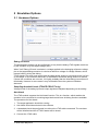
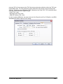
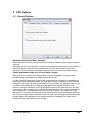
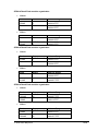
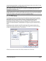
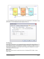
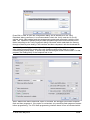
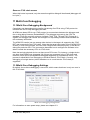
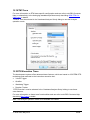
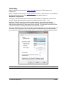
_ V9.12.225 Technical Notes ARM7/ARM9 Family On-Chip Emulation This document is intended to be used together with the CPU reference manual provided by the silicon vendor. This document assumes knowledge of the CPU functionality and the terminology and concepts defined and explained in the CPU reference manual. Basic knowledge of winIDEA is also necessary. This document deals with specifics and advanced details and it is not meant as a basic or introductory text. Contents Contents 1 1 Introduction 3 2 Emulation Options 2.1 Hardware Options 2.2 Initialization Sequence 2.3 JTAG Scan Speed 5 5 6 6 3 CPU Options 3.1 General Options 3.2 Debugging Options 3.3 Reset 3.4 NXP LPC 3.5 Advanced Options 3.6 STR9 3.7 Exceptions 9 9 10 12 13 14 15 17 4 Access Breakpoints 18 5 Hot Attach 19 6 Semihosting 20 7 Real-Time Memory Access 7.1 Introduction 7.2 Implementation 7.3 Samples 20 20 20 21 8 Internal FLASH Programming 8.1 NXP LPC2xxx Family 8.2 ST STR7 Family 8.3 ST STR9 Family 8.4 Atmel AT91SAM7S, AT91SAM7X and AT91SAM7A Series 22 22 28 30 32 9 NXP LPC32x0 ETB 35 10 JTAG Scan 37 11 Multi-Core Debugging 11.1 Multi-Core Debugging Background 11.2 Multi-Core Debugging Settings 11.2.1 Single Device Debugging in a Multi-device JTAG chain 38 38 38 39 12 Trace 12.1 ETM Trace 12.2 RTR Execution Trace 41 42 42 iSYSTEM, May 2015 1/54 13 Coverage 43 14 Profiler 44 15 Getting Started 45 16 Troubleshooting 51 17 Emulation Notes 54 iSYSTEM, May 2015 2/54 1 Introduction The JTAG interface offers all basic debug functions, based on which a debugger is implemented in winIDEA: Read and Write Memory, Read and Write Registers, Run and Stop. Single step is not supported and must be implemented by the debugger on a higher level. Two hardware breakpoints are available with ARM7, from which one is usually reserved for source debugging; the other one is available to the user. If the code is loaded into RAM, an unlimited number of software breakpoints can be set. Flash software breakpoints are also supported on some microcontroller families (Atmel SAM7, ST STR7 & STR9, NXP LPC2000). If software breakpoints are not used, the second hardware breakpoint can be freed in the Debug/Debug Options/Debugging menu by unchecking the 'Reserve one breakpoint for high level debugging' option. The ARM7TDMI core-based MCUs include the Debug Communications Channel (DCC). This is a communication channel implemented into the debug part of the MCU and enables the communication between the debugger and the MCU. The debugger communicates through the Terminal Window using JTAG, the MCU on the other side communicates through coprocessor instructions. The communication is alive when the CPU is in running mode, in stop mode there is no communication. For more information about the Terminal Window and DCC use please refer to the Software User's Guide, section 'Debug Session/Terminal Window'. Debug features: Two hardware breakpoints Unlimited software breakpoints Fast internal/external FLASH programming Software flash breakpoints (MCU Family dependant) THUMB support Hot Attach Real-time memory access through monitor Little and big endian support On-Chip Trace ARM THUMB The Thumb instruction set is a subset of the most commonly used 32-bit ARM instructions. Thumb instructions are each 16-bit long and have corresponding 32-bit ARM instruction that has the same effect on the processor model. Thumb instructions operate with standard ARM register configuration, allowing excellent interoperability between ARM and Thumb states. On execution, 16-bit Thumb instructions are transparently decompressed to full 32-bit ARM instructions in real-time, without performance loss. Thumb code is typically 65% of the size of ARM code and provides 160% of the performance of ARM code when running on a processor connected to a 16-bit memory system. Thumb therefore is an advantage in applications with restricted bandwidth, where code density is important. The availability of both 16-bit Thumb and 32-bit ARM instruction sets gives designers the flexibility to emphasize performance or code size on a subroutine level, according to the requirements of their applications. Note also that not all core registers are available in Thumb mode. iSYSTEM, May 2015 3/54 Switching from native ARM 32-bit instruction set to 16-bit Thumb and back represents some overhead for the application from the aspect of the overall performance. In the real application, the executed Thumb code should be big enough that the increase in performance due to Thumb instruction set use overcomes the loss in performance due to necessary switch from 32-bit instruction set to Thumb instruction set and switch back to native 32-bit instruction set at the end of the Thumb code. Refer to ARM Core manual for more details on Thumb mode. THUMB Code Debugging The debugging can be performed as normal. When the THUMB code is being stepped, the Data in the Code window is 16-bit long; otherwise it is 32-bit long. Not all CPU registers are available in THUMB mode, although they can be seen in the SFR window. See the THUMB section of the ARM7 manual for more information. Supported CPUs winIDEA supports all CPUs based on the ARM7DI, ARM7TDMI, ARM720T, ARM920T, ARM922T, ARM925, ARM926EJS, ARM940T, ARM946ES, ARM966ES, ARM9E and ARM9TDMI cores. Several microcontrollers have already been implemented, also with special function register (SFR) information. If a specific microcontroller is not in the CPU list, the core can be selected (i.e. ARM7TDMI, ARM7DI, etc.), the only backdraw is that the special function registers will not appear. The special function registers can be implemented for any microcontroller by request, only the SFR specification must be presented. Also custom SFR definitions can be added, see the Hardware User’s Manual for more information. Check with iSYSTEM for the latest list of supported CPUs. iSYSTEM, May 2015 4/54 2 Emulation Options 2.1 Hardware Options Debug I/O levels The development system can be configured in a way that the debug JTAG signals are driven by the emulator or by the target voltage (Vref). When 'Vref' Debug I/O level is selected, a voltage applied to the belonging reference voltage pin on the target debug connector is used as a reference voltage for voltage follower, which powers buffers, driving the debug JTAG signals. The user must ensure that the target power supply is connected to the Vref pin on the target JTAG connector and that it is switched on before the debug session is started. If these two conditions are not meet, it is highly probably that the initial debug connection will fail already. However in some cases it may succeed but then the system will behave abnormal. Sampling threshold levels (iTRACE PRO/GT only) Voltage levels of the debug input and output signals are adjusted depending on the setting. Hot Attach The JTAG module supports the Hot Attach function. This is a function, which enables the emulator to be connected to a working target device and have all debug functions available. The procedure for Hot Attach: 1. The target application should be running. 2. Hot Attach should be selected in the software. 3. A download should be performed, but without the JTAG cable connected. The emulator will be initialized and the ATTACH status will be shown. 4. Connect the JTAG cable. iSYSTEM, May 2015 5/54 5. Select the Attach option in the Debug menu. When this option is selected, the emulator tries to communicate through JTAG. If it is successful, it shows the STOP or RUNNING status. At this point, all debug functions are available. 6. When the debugging is finished, the CPU should be set to running and Detach selected from the Debug menu. The status shown is ATTACH. Now the JTAG cable can be safely removed. If Hot attach is used, please refer to Hot Attach chapter for more details. Note: Hot Attach function cannot be used for any flash programming or code download! 2.2 Initialization Sequence The user must properly configure the CPU before the debug download (including the flash programming) can take place to the memory area, which is not accessible upon the CPU reset. This is essential for the applications using memory resources, for instance external RAM or external flash, which are not accessible after the CPU reset. In such case, the debugger executes a so-called initialization sequence immediately after the CPU reset, which writes to the CPU registers configuring the CPU memory interface to the physical memory and then the debug download is executed. Note that the initialization sequence must be set up specific to the application. Besides enabling a disabled memory access upon reset, the initialization sequence can also be used for instance to disable the CPU internal watchdog being active after reset or to modify any other CPU registers, when it’s preferred to run the application with the modified CPU reset state. Detailed information may be found in the Initialization Sequence help topic. 2.3 JTAG Scan Speed JTAG Scan Speed definition Scan speed The JTAG chain scanning speed can be set to: Slow - long delays are introduced in the JTAG scanning to support the slowest devices. JTAG clock frequency varying from 1 kHz to 2000 kHz can be set. iSYSTEM, May 2015 6/54 Fast – the JTAG chain is scanned with no delays. Burst – provides the ability to set the JTAG clock frequency varying from 4 MHz to 100 MHz. Burst+ - provides the ability to set the JTAG clock frequency varying from 4 MHz to 100 MHz RTCK - Adaptive RTCK clocking for ARM Free – this mode is not supported for ARM JTAG debug interface Slow and Fast JTAG scanning is implemented by means of software toggling the necessary JTAG signals. Burst mode is a mixture of software and hardware based scanning and should normally work except when the JTAG scan frequency is an issue that is when the JTAG scan frequency used by the hardware accelerator is too high for the CPU. In general, selecting an appropriate scan frequency usually depends on scan speed limitations of the CPU. In Burst+ mode, complete scan is controlled by the hardware accelerator, which poses some preconditions, which are not met with all CPUs. Consequentially, Burst+ mode doesn’t work for all CPUs. Burst and Burst+ are not supported on iONE debug tool. RTCK speed mode is available for ARM family only and is intended for targets which use widely varying system clock during a debug session. For example, if the CPU switches to different power modes and changes system clocks, the debugger will be able to maintain synchronization with on-chip debug interface even at much slower clock. The target CPU needs to provide RTCK synchronization signal, which must be available on pin 11 on standard 20-pin ARM JTAG debug connector. RTCK clock option is available for all development systems except for older iC3000 ARMx iCARD based development system. Due to extra synchronization, top speed using "RTCK" mode is about half as fast as "Fast" mode. In general, Fast mode should be used as a default setting. If the debugger works stable with this setting, try Burst or Burst+ mode to increase the download speed. If Fast mode already fails, try Slow mode at different scan frequencies until you find a working setting. Use – Scan Speed during Initialization On some systems, slower scan speed must be used during initialization, during which the CPU clock is raised (PLL engaged) and then higher scan speeds can be used in operation. In such case, this option and the appropriate scan speed must be selected. Configuring JTAG Scan speed for the first time Sometimes, the default JTAG scan speed needs to be changed. A default ‘Fast’ JTAG scan speed may not work for all ARM CPUs. WinIDEA may report a message “Error 175: JTAG chain error. Check target VCC and Emulation Options/JTAG Position” when the debug connection cannot be established due to too high debug JTAG scan speed. Select ‘Slow’ JTAG scan speed and try different possible JTAG frequencies when initial debug connection cannot be established. NXP LPC2xxx family usually requires ‘Slow’ JTAG scan speed. In general, it is recommended to use the highest working JTAG scan speed for the optimal debug performance. ST STR91xF Family The two dies inside the STR91xF (CPU die and Flash memory die) are internally daisychained on the JTAG bus. The CPU die has two JTAG Test Access Ports (TAPs), one for boundary scan functions and one for ARM CPU debug. The Flash memory die has one TAP for program/erase of non-volatile memory. Because these three TAPs are daisy-chained, iSYSTEM, May 2015 7/54 only one TAP will converse on the JTAG bus at any given time while the other two TAPs are in BYPASS mode. The TAP positioning order within this JTAG chain is the boundary scan TAP first, followed by the ARM debug TAP, followed by the Flash TAP. TAP controllers have following JTAG instruction register length: - Flash TAP: 8 bits - Boundary scan TAP: 5 bits - ARM CPU debug TAP: 4 bits In order to debug ARM core, the user must set 8 for IR prefix and 5 for IR Postfix in winIDEA 'Hardware/Emulation Options/JTAG' dialog. iSYSTEM, May 2015 8/54 3 CPU Options 3.1 General Options Hard Interrupt Disable When Stopped When this option is checked interrupts will be enabled immediately after program execution resumes. Otherwise, the CPU must execute a couple of instructions before returning to the program to determine whether interrupts were enabled when the CPU was stopped. These extra instruction executions can prevent task preemption when an interrupt is already pending. Cache downloaded code only (do not load to target) When this option is checked, the download files will not propagate to the target using standard debug download but the Target download files will. In cases, where the application is previously programmed in the target or it's programmed through the flash programming dialog, the user may uncheck 'Load code' in the 'Properties' dialog when specifying the debug download file(s). By doing so, the debugger loads only the necessary debug information for high level debugging while it doesn't load any code. However, debug functionalities like ETM and Nexus trace will not work then since an exact code image of the executed code is required as a prerequisite for the correct trace program flow reconstruction. This applies also for the call stack on some CPU platforms. In such applications, 'Load code' option should remain checked and 'Cache downloaded code only (do not load to target)' option checked instead. This will yield in debug information and code image loaded to the debugger but no memory writes will propagate to the target, which otherwise normally load the code to the target. iSYSTEM, May 2015 9/54 3.2 Debugging Options Execution Breakpoints Hardware Breakpoints Hardware breakpoints are breakpoints that are already provided by the CPU. The number of hardware breakpoints is limited to two. The advantage is that they function anywhere in the CPU space, which is not the case for software breakpoints, which normally cannot be used in the FLASH memory, non-writeable memory (ROM) or self-modifying code. If the option 'Use hardware breakpoints' is selected, only hardware breakpoints are used for execution breakpoints. Note that the debugger, when executing source step debug command, uses one breakpoint. Hence, when all available hardware breakpoints are used as execution breakpoints, the debugger may fail to execute debug step. The debugger offers 'Reserve one breakpoint for high-level debugging' option in the Debug/Debug Options/Debugging' tab to circumvent this. By default this option is checked and the user can uncheck it anytime. Software Breakpoints ARM7 and ARM9 cores provide two hardware breakpoints, which often prove insufficient. The debugger can use unlimited software breakpoints to work around this limitation. Note: ARM has no dedicated breakpoint instruction. Instead an invalid op-code is used and one hardware breakpoint is configured to trigger when this instruction is fetched. Thus only one hardware breakpoint remains available for hardware execution breakpoints, access breakpoints and trace trigger. If breakpoints are expected to be set only in areas, where software breakpoints cannot be used, it is advised to turn software breakpoints off, since this will enable the usage of the hardware breakpoint that is normally reserved. When a software breakpoint is being used, the program first attempts to modify the source code by placing a break instruction into the code. If setting software breakpoint fails, a hardware breakpoint is used instead. iSYSTEM, May 2015 10/54 Note that the debugger additionally features unlimited software breakpoints in the internal CPU flash for following families: NXP LPC2000, ST STR7, Atmel AT91SAM7S, Atmel AT91SAM7A and Atmel AT91SAM7X. Time to set or clear the breakpoint depends on the debug JTAG scan speed, CPU clock and flash sector size. Set/clear SW BPs before Run When the option is checked, then a software breakpoint is not set/cleared immediately, but is just remembered. Only when the CPU is set to running are the breakpoints committed. This way several breakpoints can be changed but only one re-FLASH operation takes place. This is especially noticeable in testIDEA operation with many stubs and also during a regular debugging session when several breakpoints are set/cleared within the same flash erase block. Simulate instr. step ‘Never’ is selected per default. When run or source step debug command is executed from a BP location, the debugger first clears BP, executes single step, sets back the original BP and then resumes the application. All this is done in background hidden from the user. Since setting and clearing software flash breakpoint is time consuming, a new approach was introduced, which simulates the first instruction at breakpoint address without requiring clearing and setting the software flash breakpoint. Thereby, the user can select ‘FLASH SW BP’ in order to speed up the debugging. If the option yields erroneous behavior, set back to the default setting. Ext. Oscillator clk Before performing first debug download, which also programs the code into the flash, the user must enter frequency of the external oscillator connected to the target CPU. Based on this value, flash programming procedure will calculate CPU frequency whenever it’s necessary and feed it to the NXP API functions which are used for programming the flash and are part of the CPU firmware already. Note: This setting is available only for NXP devices and at the same time obligatory for these devices. Boost CPU clock after RESET Flash programming can be speed up by raising CPU frequency via CPU PLL module before flash programming takes place. This is done by checking the ‘Boost CPU clock after RESET’ option The debugger enables and configures CPU PLL before the flash programming is started. Note that the CPU PLL remains configured after the debug download and the debug reset. Therefore it cannot be assumed that the PLL is disabled when the user opens a debug session to debug the application code. The user startup code must follow the steps described in the CPU User Manual to disconnect the PLL and reconfigure it. Note: This option is available for NXP devices only. Ignore Access errors When checked, the debugger identifies memory access errors for individual memory location(s). When the option is unchecked, the debugger would declare access error for remaining memory locations once one access error is detected within a memory read block, which is used in the disassembly window or memory window. iSYSTEM, May 2015 11/54 3.3 Reset Latch target RESET When the option is checked (default), the debugger latches active target reset until it gets processed. This yields a delay between the target reset and restart of the application from reset. If this delay is not acceptable for a specific application, the option should be unchecked. An example is an application where the CPU is periodically set into a power save mode and then waken up e.g. every 6ms by an external reset circuit. In such case, a delay introduced by the debugger would yield application not operating properly. When the option is unchecked, it may happen that the debugger does not detect the target reset although the CPU gets reset. The debugger polls the CPU status ~3 times per second while the target reset can occur in between. RESET Duration The width of the RESET pulse is specified here. Post RESET Delay Typically, the on-chip debug module is reset concurrently with the CPU. After the debugger releases the CPU reset line from the active state, the on-chip debug module can require some time (delay) to become operational. This time can also depend on any additional reset circuitry on the target system. The default delay value normally allows the debugger to gain the control over the CPU. If a debug connection fails, try different delay values to try and establish the debug connection. RESET Method Typically an ARM CPU has two reset signals connected to the standard ARM debug connector. ARM debug connector defines NTRST and NSRST lines. NTRST reset line controls on-chip debug module, a so-called EmbeddedICE. Whenever a low level is asserted on this line, the on-chip debug logic is reset. An external debugger controlling the application drives this line. NSRST is a system reset and connected to the CPU reset line. An external debugger and/or other target reset sources drive this CPU reset line. How the debugger iSYSTEM, May 2015 12/54 gains the control over the application? First, the debugger asserts both reset lines to reset both, the CPU and on-chip debug module. Then it releases the NTRST line which yields in initialized on-chip debug module. Next, it sets an execution breakpoint at address 0x0, which is a CPU start address out of the reset. Finally, NSRST line is released and the CPU stops at breakpoint (address 0x0). At this moment the debugger has complete control over the application. Now, an initialization sequence can be executed (if required) and debug download carried out. In such applications 'Regular' reset method should be selected. Some CPUs (NXP LPC2000, Atmel AT91) don't provide NTRST pin externally. In such cases, it's typically connected to the NSRST internally. Such applications behave differently from the one just being described. Major difference is that the debugger cannot gain the control over the CPU immediately after it starts to run out of the reset. After the CPU reset (NSRST) is released, the on-chip debug module needs some time to become initialized and operational. The application cannot be controlled (stopped) as long as the debug module is not operational. With some delay the debugger takes the control over the CPU by forcing stop command over the debug JTAG interface and presetting program counter to the reset value. Such system exhibits short program execution out of the reset and it may not be in its reset state any longer. Note that this undesired program execution might impact on CPU registers and their reset values, CPU memory mapping, etc. In worst case, the CPU may even hang due to no valid code. This applies for any application where the program starts in a memory, which doesn't contain any code on power up, e.g. empty flash or RAM. In such applications it's recommended to use 'Stop and Preset' reset method. Then the debugger presets only program counter (PC/R15) on 'debug reset' or 'debug download' command once it gains the control over the CPU. Try different 'reset delay' values if it looks like that the CPU hangs while the debugger tries to gain the control over the CPU. 3.4 NXP LPC NXP LPC tab becomes available when NXP LPC21/22/23/24xx family is selected in the ‘Hardware/Emulation Options’ dialog. Preset MEMMAP / SYSMEMREMAP When the option is checked the debugger presets the CPU MEMMAP register. iSYSTEM, May 2015 13/54 Note: This option is available for NXP LPC2xxx devices only. 3.5 Advanced Options ARM Family Advanced options Override startup register values This option overrides the default Program Counter reset value with the value set. Force Supervisor mode while stopped If this option is checked, Supervisor mode is forced while the application is stopped. Allow real-time memory access via DCC If this option is checked, the DCC channel is used for real-time memory access. Use Handshaking When this option is checked, execution of every command is handshaked. This is required by CPUs for which the JTAG clock is too high. iSYSTEM, May 2015 14/54 3.6 STR9 STR9 tab becomes available when ST STR9 family is selected in the ‘Hardware/Emulation Options’ dialog. Mass erase before download Both flash banks are erased before the download when the option is checked. CSx Mapping Depending on the selection, CSx bit is programmed before every debug reset and debug download. Don’t forget that boot bank respectively mapping of the flash Bank 0 and Bank 1 is defined by CSx bit, non-volatile Flash based configuration bit. The firmware cannot change this configuration bit, only the JTAG interface has access. Note: Cortex debug iCARD does not support programming the ‘CSx Mapping’ bit. winIDEA complies with the following STR9 memory mapping: iSYSTEM, May 2015 15/54 STR91xFAxx2 Flash module organization CSx=0 Bank Bank 0 256kB Bank 1 32kB Sector 64kB Sectors 03 8kB Sectors 0-3 Address Range 0x0000.00000x0003.FFFF 0x0004.00000x0004.7FFF Bank Bank 1 32kB Sector 8kB Sectors 0-3 Bank 0 256kB 64kB Sectors 03 Address Range 0x0000.00000x0000.7FFF 0x0004.00000x0007.FFFF CSx=1 STR91xFAxx4 Flash module organization CSx=0 Bank Bank 0 512kB Bank 1 32kB Sector 64kB Sectors 07 8kB Sectors 0-3 Address Range 0x0000.00000x0007.FFFF 0x0008.00000x0008.7FFF Bank Bank 1 32kB Sector 8kB Sectors 0-3 Bank 0 512kB 64kB Sectors 07 Address Range 0x0000.00000x0000.7FFF 0x0008.00000x000F.FFFF CSx=1 STR91xFAxx6 Flash module organization CSx=0 Bank Bank 0 1024kB Bank 1 128kB Sector 64kB Sectors 015 16kB Sectors 07 Address Range 0x0000.00000x000F.FFFF 0x0010.00000x0011.FFFF Sector 16kB Sectors 07 64kB Sectors 015 Address Range 0x0000.00000x0001.FFFF 0x0010.00000x001F.FFFF CSx=1 Bank Bank 1 128kB Bank 0 1024kB iSYSTEM, May 2015 16/54 STR91xFAxx7 Flash module organization CSx=0 Bank Bank 0 2048kB Bank 1 128kB Sector 64kB Sectors 031 16kB Sectors 07 Address Range 0x0000.00000x001F.FFFF 0x0020.00000x0021.FFFF Sector 16kB Sectors 07 64kB Sectors 031 Address Range 0x0000.00000x0001.FFFF 0x0020.00000x003F.FFFF CSx=1 Bank Bank 1 128kB Bank 0 2048kB Note: When performing download into the STR9 flash, only above memory regions are valid. 3.7 Exceptions With the ARM9 family of products exceptions can be defined. CPU setup, Exceptions menu The debug mode will be entered (that is, the application will be stopped) on any exception selected. iSYSTEM, May 2015 17/54 4 Access Breakpoints ARM Hardware Breakpoints menu Condition Both internal ARM7 watchpoints can be used. Select the watchpoint combination that triggers the breakpoint. Note: Refer to the ARM CPU manual for explanation of the RANGE mode. WP0 and WP1 Specify the address and data bus states to monitor for the watchpoints. Address The address of the access breakpoint is entered here. The mask can be also set. The mask 0 ignores all bits of the address; the mask FFFFFFFF uses all bits of the address. Data Value The data, which triggers the breakpoint, is entered here. The mask can be also set. The mask 0 ignores all bits of the value; the mask FFFFFFFF uses all bits of the value. Access, Bus Cycle, Access Width, Mode, External Input The masks to be monitored. iSYSTEM, May 2015 18/54 When Breakpoints Occur A beep can be issued and/or a message displayed indicating that an access breakpoint has occurred. Wizard… Use Wizard in case of problems understanding and configuring the access breakpoints dialog. It helps setting a simple a breakpoint on data access or code execution. 5 Hot Attach The Hot Attach function can be enabled for troubleshooting purposes. The full hot attach is not supported, which means that the target must be first connected to the emulator and then turned on. The target must be functional, which means that it must contain a FLASH with a working code. First, make sure the Hot Attach to Target function in the Hardware/Emulation Options/Hardware dialog is turned on (checked). Typical usage, with the emulator turned on: turn the init sequence off erase the download file turn on the target invoke Reset now the emulator must be able to read the status – typically Running or Reset will be shown in the status. If the target is running, it can now be stopped with the Stop command. If the stop has succeeded, the debugging is operational (including breakpoints, stepping, etc.). With this function, the debugger does not set breakpoints to Reset or in any other way manipulates with the internal debug logic. This function is limited to polling the status of the internal CPU logic (Embedded ICE). This is especially useful for initializing and troubleshooting, on the other hand for normal debugging this option should be turned off. Note: Hot Attach function cannot be used for any flash programming or code download! iSYSTEM, May 2015 19/54 6 Semihosting ARM semihosting is feature that can be used with ARM 1.2 compiler tools and enables the user to use standard C functions (printf, fopen …) in embedded target. Calls from these functions are routed from program running on the target through CPU JTAG port and emulator to winIDEA that will actually execute them. Terminal window is used as standard input/output in this case. Refer also to ARM toolset manual for detailed description of the semihosting concept and implementation. The options for the Terminal are configured in the Terminal Options page. Semihosting terminal configuration 7 Real-Time Memory Access 7.1 Introduction Standard JTAG debug hardware on ARM based CPUs does not implement support for realtime memory access in hardware. Therefore a software based approach has to be used to provide this feature. This means is that with this approach, winIDEA debugger can also perform memory read and write accesses while the target system CPU is running, not just when the CPU is stopped. This feature allows for additional ways of debugging and controlling the target application. For example, target application parameters can be changed while the application is running. Or external client applications using iSYSTEM's iCONNECT interface can constantly gather data from a running application as well as change application's operating parameters. 7.2 Implementation winIDEA host debugger uses a small debug monitor program that must be included in the target system software to provide run-time services for the debugger. winIDEA and debug monitor communicate using debug communications channel (DCC) present in standard ARM iSYSTEM, May 2015 20/54 EmbeddedICE debug hardware. This of course means that when real-time feature is used, DCC cannot be used for any other purpose (i.e. terminal window in winIDEA). The debug monitor code is provided by iSYSTEM to customers who wish to use this feature in their systems. A set of distributable files is provided for inclusion in customer projects: dbgmon_arm.c, dbgmon_arm.h - for use as C/C++ source. dbgmon_armgnu.asm - for use as assembly language source (provided file is in GNU assembly format, but simple to tailor to other assembly formats) Simply include the appropriate files in your project and setup calls to monitor init function and the periodic service procedure. Debug monitor code itself is provided in these sources in binary format as an array of 32-bit words. Debug monitor also requires a small data area (256 bytes) for operation. This data area is also allocated in the provided source files. Debug monitor provides two entry points: first one is the initialization and the second one is the periodic service procedure. The initialization procedure must be called only once and before the service procedure is called for the first time. After that, service procedure should be invoked periodically to allow the monitor to service requests from host debugger winIDEA. Further detailed implementation notes are provided in each source file. The rate at which the periodic service procedure should be called depends on the required real-time responsiveness, throughput and allowed overhead for the target application. The more often the service procedure is called the higher the rate of memory transfers can be. On the other hand, this also means more overhead for the target application in terms of cycles stolen to service real-time access requests. Every time the service procedure is invoked it uses approximately 25 cycles even if no operation is requested by host debugger. If host debugger does request an operation, the number of consumed cycles depends on the kind of operation. The highest number of cycles consumed in one invocation of service procedure is about 50. 7.3 Samples Two sample projects are provided with winIDEA to demonstrate the real-time access feature itself and to provide an example of how the debug monitor can be integrated into the target system application. One sample uses the C source version of debug monitor files; the other sample uses the assembly language version of debug monitor files. Both samples were developed on ARM920T-based Samsung S3C2410X platform. They both use a timer to generate an IRQ interrupt to periodically invoke the debug monitor service procedure which handles requests from the host debugger - winIDEA while the target is running. Timer configuration is performed from the ini script and is setup to trigger an interrupt approximately once every millisecond. iSYSTEM, May 2015 21/54 8 Internal FLASH Programming 8.1 NXP LPC2xxx Family The target application may not run from the internal flash due to various factors. The following text might be very helpful when troubleshooting the CPU startup problems. Refer to the CPU User Manual for more details on the CPU startup. The flash boot loader code is executed every time the CPU is powered or reset. The loader can execute the ISP (In-System Programming) command handler or the user application code. P0.14 is sensed on a rising edge on the RST (CPU reset) pin. If a low level is detected, ISP command handler starts and takes over control of the CPU after reset. If there is no request for the ISP command handler execution (a high-level detected), a search is made for a valid user program. If a valid user program is found then the execution control is transferred to it. Criterion for valid user code: The reserved ARM interrupt vector location (0x14) should contain the 2’s complement of the check-sum of the remaining interrupt vectors. This causes the checksum of all of the vectors together to be 0. The boot loader code disables the overlaying of the interrupt vectors from the boot block, then checksums the interrupt vectors in sector 0 of the flash. If the signatures match then the execution control is transferred to the user code by loading the program counter with 0x0000 0000. Hence the user flash reset vector should contain a jump instruction to the entry point of the user application code. If the signature is not valid, the auto-baud routine synchronizes with the host via serial port 0. The debugger programs the code directly into the internal flash memory through the standard debug download. Based on the selected CPU, the debugger identifies which code from the download file fits into the internal flash, and loads it to the flash through the flash programming procedure hidden to the user. The flash programming procedure is implemented using NXP IAP (In-Application Programming) interface being already part of the CPU Flash Boot Loader firmware. All other code, allocated outside of the flash boundaries, is downloaded to the target through standard the memory writes. Note: Proper target CPU must be selected in the ‘Hardware/Emulation Options’ dialog since corresponding flash programming procedure is selected based on the selected CPU. Due to the CPU requirements, winIDEA extracts the necessary interrupt vectors from the download file before programming a 32-bit value to the 0x14 address, makes the 2’s complement of the check-sum of these vectors and programs the calculated value to the 0x14 address. This yields the CPU starting from the user code after the reset. Consequentially, if ‘Verify download’ is executed after the debug download, the user normally gets error for 4 bytes at address 0x14 since the programmed value doesn’t match with the one in the download file. The user can ignore the error or adjust his download file in a way that a 32-bit value at the address 0x14 contains proper value, which results in the CPU start executing the user code after the reset. The alternative is also to skip verifying 4 bytes at address 0x14. Next picture shows the necessary setting in the Download dialog. iSYSTEM, May 2015 22/54 In practice, there is no need for ‘Verify download’ after the debug download since winIDEA flash programming procedure verifies programmed code within the procedure itself and reports any errors in the Progress dialog during the download. Code Read Protection Code Read Protection is enabled by programming the flash address location 0x1FC with value 0x87654321. Address 0x1FC is used to allow some room for the fiq exception handler. When the code read protection is enabled the JTAG debug port, external memory boot and few ISP commands are disabled. The ISP erase command only allows erasure of all user sectors when the code read protection is enabled. This limitation does not exist if the code read protection is not enabled. IAP commands are not affected by the code read protection. Note: Be precautious not to accidentally write 0x87654321 at 0x1FC as this disables the JTAG debug port. The backdoor is to erase the flash through the ISP interface (serial port 0). Setting Up Flash Programming Note: Necessary settings related to the LPC2xxx flash programming have changed as of winIDEA build 9.10.83. Select the NXP LPC21/22/23/24xx family in the CPU list and select specific target CPU in the ‘Custom CPU variant’ combo box. iSYSTEM, May 2015 23/54 Before performing first debug download, which also programs the code into the flash, the user must enter frequency of the external oscillator connected to the target CPU. Based on this value, flash programming procedure will calculate CPU frequency whenever it’s necessary and feed it to the NXP API functions which are used for programming the flash and are part of the CPU firmware already. After reset the LPC2xxx CPU operates at relatively slow frequency comparing to the maximum CPU frequency. For this reason, debugger must use relatively slow JTAG scan speed to communicate with the CPU over the debug interface. iSYSTEM, May 2015 24/54 Flash programming can be speed up by raising CPU frequency via CPU PLL module before flash programming takes place. This is done by checking the ‘Boost CPU clock after RESET’ option in the ‘Debugging’ tab. The debugger enables and configures CPU PLL before the flash programming is started. Note that CPU PLL remains configured after the debug download and the debug reset. Therefore it cannot be assumed that the PLL is disabled when the user opens a debug session to debug the application code. The user startup code must follow the steps described in the CPU User Manual to disconnect the PLL and reconfigure it when used by the target application too. With ‘Boost CPU clock after RESET’ option checked, the user may try to increase JTAG scan speed of the debug interface. This should work if target application uses PLL too. iSYSTEM, May 2015 25/54 With above settings, the debugger uses slow JTAG scan speed only for the initial debug connection and initialization, while for debug download including flash programming and later CPU control use Fast JTAG scan speed. Note: For the internal flash programming requirements, the user doesn’t need to setup any debug initialization sequence (.ini). There is additional flash programming related setting, which affects the target CPU. It concerns the MEMMAP register. The MEMMAP register controls the mapping of the bottom memory including default reset and interrupt vectors. If the option is checked, the debugger presets the MEMMAP register after the CPU reset before any other debug action takes place. iSYSTEM, May 2015 26/54 If ‘Preset MEMMAP / SYSMEMREMAP’ option is not checked, flash programming procedure sets MEMMAP value to 1 (flash visible at 0x0), programs the flash and then restores the original MEMMAP register value. Such setting would yield verify errors, if debug verify is performed after the debug download, when programming an empty flash on LPC213x device or regular programming on LPC2294 despite the fact that the flash was programmed properly. It’s because the flash programming procedure restores original reset MEMMAP register before the debug verify is performed and in these two cases this yields flash memory no longer visible at the time of the debug verify. Note that after reset, erased LPC213x device boots with MEMMAP=0 and LPC229x device boots with MEMMAP = 0x3. In such case it might be more predictable behavior when the ‘Preset MEMMAP / SYSMEMREMAP’ option is checked and CPU keeps this value after the debug download too. Based on the selected CPU, belonging flash device occurs in the ‘FLASH Setup…’ dialog (Hardware menu). Press Edit in order to open the configuration dialog. As an alternative to the ‘Verify Download‘ debug command, it is recommended to check the ‘Verify‘ and the ‘On the fly’ options, which yield reading back the programmed content and comparing it with the input data during the write process. This operation is performed by the flash programming monitor and is thereby much faster comparing to the ‘Verify Download‘ debug command, which reads back the memory through a relatively slow debug JTAG interface and then compares it with the download file. Note: ‘Verify on the fly’ performed by the flash programming monitor will not report errors when debug download file contains the code residing outside of the flash (e.g. code exceeding the physical flash). It verifies only the code that gets written into the flash. For that purpose, the 'Debug/Verify' is the foolproof tool to use. iSYSTEM, May 2015 27/54 When ‘Mass erase before download’ option is checked, the debugger first erases complete flash and then programs it. If the option is unchecked, only necessary flash sectors are erased before the programming. Troubleshooting If flash cannot be programmed, first perform debug reset only, then open memory window at address 0x4000_0000 and try to modify the content. If there are problems already, try to decrease JTAG scan speed and try different reset duration and post reset delay. In case of problems with the flash programming, double check that the application does not enable the internal watchdog. This would conflict with the flash programming especially if that is performed shortly after the CPU reset. The debugger cannot take control over the microcontroller immediately after the CPU reset but takes some time, which means some application code is executed before the microcontroller takes the control over. If that code enables the watchdog, flash programming will fail. If the watchdog is enabled later on in the application this will also conflict with the debugger, which must have complete control over microcontroller all the time. Therefore, when debugging the application, the internal watchdog must not be enabled (after reset it’s disabled). It has been noticed that flash programming on LPC2103 fails at default CPU reset frequency. The solution is to check the ‘Boost CPU clock after RESET’ option. 8.2 ST STR7 Family The debugger loads the code directly into the internal flash memory through the standard debug download. Based on the selected CPU, the debugger identifies which code from the download file fits into the internal flash, and loads it to the flash through the flash programming procedure hidden to the user. The flash programming procedure is implemented through the CPU Flash registers (FLASH_CR0, FLASH_DR0, etc.). All other iSYSTEM, May 2015 28/54 code, allocated outside of the flash boundaries, is downloaded to the target through the standard memory writes. When a new project is started, flash programming must be configured first. Based on the selected CPU, belonging flash device occurs in the ‘FLASH Setup…’ dialog (Hardware menu). Press Edit in order to open the Device configuration dialog. As an alternative to the ‘Verify Download‘ debug command, it is recommended to check the ‘Verify‘ and the ‘On the fly’ options, which yield reading back the programmed data after the write command ends and comparing it with the data, which is still kept in the flash programming data buffer. This operation is performed by the flash programming monitor and is thereby much faster comparing to the ‘Verify Download‘ debug command, which reads back the memory through a relatively slow debug JTAG interface and then compares it with the download file. Note: ‘Verify on the fly’ performed by the flash programming monitor will not report errors when debug download file contains the code residing outside of the flash (e.g. code iSYSTEM, May 2015 29/54 exceeding the physical flash). It verifies only the stuff that gets written into the flash. For that purpose, the 'Debug/Verify' is the foolproof tool to use. When ‘Mass erase before download’ option is checked, the debugger first erases complete flash and then programs it. If the option is unchecked, only necessary flash sectors are erased before the programming. The STR7 internal flash starts at an absolute address 0x4000 0000 and there is a mirrored image at address 0x0. Per default, the debugger expects the code to be linked and loaded at 0x4000 0000. When the code is linked to the mirrored address range (0x0), the user should set 0 for the ‘Address in CPU space’ in the Device configuration dialog. 8.3 ST STR9 Family The debugger loads the code directly into the internal flash memory through the standard debug download. Based on the selected CPU, the debugger identifies which code from the download file fits into the internal flash, and loads it to the flash through the flash programming procedure hidden to the user. The flash programming procedure is implemented using flash programming libraries provided by ST. All other code, allocated outside of the flash boundaries, is downloaded to the target through the standard memory writes. STR9 family must be selected in the CPU list and target CPU must be selected in the ‘Custom CPU variant’ combo box. Make sure that correct target CPU is selected because complete flash programming relies on this selection. STR9 microcontroller has three JTAG TAPs connected in the JTAG chain. iSYSTEM, May 2015 30/54 To access ARM debug module, IR Prefix must be set to 8, DR Prefix to 1, IR Postfix to 5 and DR Postfix to 1 in the ‘Hardware/Emulation Options/JTAG’ tab. CSx Mapping Depending on the selection in the ‘Hardware/Emulations Options/CPU Setup/STR9’ tab, CSx bit is programmed before every debug reset and debug download. Don’t forget that boot bank respectively mapping of the flash Bank 0 and Bank 1 is defined by CSx bit, non-volatile Flash based configuration bit. The firmware cannot change this configuration bit, only the JTAG debug interface has access. Mass Erase Mass Erase can be issued on request at any time via ‘Hardware/STR9 FLASH -> Mass Erase’ button. iSYSTEM, May 2015 31/54 Unsecure Unsecure operation, which can be issued on request via ‘Hardware/STR9 FLASH -> Unsecure’ button, performs mass erase of the MCU flash over the JTAG interface. Unsecure operation should be performed as part of the troubleshooting procedure, when there are problems with flash programming or initial debug connection. There are security related registers, which could be accidentally put into the state, which protects the flash from being programmed. These registers get erased only by mass erase performed over the JTAG interface. Note: Cortex debug iCARD does not support Unsecure operation. 8.4 Atmel AT91SAM7S, AT91SAM7X and AT91SAM7A Series First of all, the internal watchdog needs to be disabled to be able to debug these CPUs and program the internal flash.. Next, CPU needs to be configured before the flash can be programmed. Proper FMCN value must be set in the Flash Mode Register (MC_FMR) depending on the CPU clock otherwise the flash programming fails. Refer to the CPU datasheet for more details on MC_FMR configuration and the FMCN value. Since the CPU starts at slow clock it’s recommend to speed up the CPU before the flash programming takes place. Otherwise the flash programming can take place quite a while. Excerpt from the initialization file (AT91SAM7S64.ini) from the AT91SAM7S64 sample project: WDT_MR L 0x8000 // disable watchdog A MC_FMR L 0x100000 // flash mode register - set FMCN properly !! A CKGR_MOR L 0x00000601 // oscillator enable, 48 (6x8) cycles start-up time A PMC_MCKR L 0x5 // main oscillator selected and main clock divided by 2 The debugger loads the code directly into the internal flash memory through the standard debug download. Based on the selected CPU, the debugger identifies which code from the download file fits into the internal flash, and loads it to the flash through the flash programming procedure hidden to the user. The flash programming procedure is implemented through the CPU Flash registers (FLASH_CR0, FLASH_DR0, etc.). All other code, allocated outside of the flash boundaries, is downloaded to the target through the standard memory writes. When a new project is started, flash programming must be configured first. Based on the selected CPU, belonging flash device occurs in the ‘FLASH Setup…’ dialog (Hardware menu). iSYSTEM, May 2015 32/54 Press Edit in order to open the configuration dialog. As an alternative to the ‘Verify Download‘ debug command, it is recommended to check the ‘Verify‘ and the ‘On the fly’ options, which yield reading back the programmed content and comparing it with the input data. This operation is performed by the flash programming monitor and is thereby much faster comparing to the ‘Verify Download‘ debug command, which reads back the memory through a relatively slow debug JTAG interface and then compares it with the download file. Note: ‘Verify on the fly’ performed by the flash programming monitor will not report errors when debug download file contains the code residing outside of the flash (e.g. code exceeding the physical flash). It verifies only the stuff that gets written into the flash. For that purpose, the 'Debug/Verify' is the foolproof tool to use. When ‘Mass erase before download’ option is checked, the debugger first erases complete flash and then programs it. If the option is unchecked, only necessary flash pages are erased before programming. The CPU flash programming interface doesn’t have a command which iSYSTEM, May 2015 33/54 would only erase individual flash pages. A page can be erased only in combination with the flash program command. Troubleshooting Flash programming can fail due to: 1) Incorrect FMCN value in the MC_FMR register 2) Improper JTAG scan speed (try different JTAG scan speeds to see if it makes any difference!) 3) Locked flash regions For instance, the AT91SAMS256 flash is divided into 16 flash lock regions and each can be protected in order to protect the pages within the region from being erased or programmed. Note that after the production, the device may have some embedded Flash lock regions locked. These locked regions are reserved for a default application. Locked sectors can be unlocked to be erased and then programmed. Note: The ‘Mass erase’ command is canceled when at least one page is locked. The debugger cannot detect when ‘Mass erase’ is canceled due to the locked region. Consequentially, when the Mass Erase command is used while one or more regions are locked, the debugger reports successful erasing although the flash was not erased. The user should have this in mind. Devices with 512 kB of flash expect the code to be linked at address 0x100000, where the flash is physically located. However, the flash has also a mirror image at 0x0 and some users might link the target application to 0x0. In such case, the debugger must be adjusted accordingly. Change the flash address offset from default 0x100000 to 0x0 (‘Address in CPU space’ field) and then also a download file linked to the address 0x0 will be successfully programmed into the flash. iSYSTEM, May 2015 34/54 9 NXP LPC32x0 ETB As process speeds increase it is increasingly difficult to obtain trace information off a chip from an Embedded Trace Macrocell (ETM). This causes difficulties in maintaining acceptable signal quality or the signals need to be demultiplexed on to what can become a very large number of trace port pins. The solution is to provide a buffer area on-chip where the trace information is stored, and read from the chip later, at a slower rate. The ETB (Embedded Trace Buffer) stores data produced by the ETM. The buffered data can then be accessed by the debugging tools using a JTAG debug interface. Providing an on-chip buffer enables the trace data generated by the ETM (at the system clock rate) to be read by the debugger (e.g. iC3000 & ARM iCARD or iC5000 development system) at a reduced clock rate. This removes the requirement for high-speed pads for the trace data. The NXP LPC32x0 ETB has a 2048 × 24 bit RAM for instruction/data history storage With winIDEA 2010 a dedicated CPU selection for NXP LPC32x0 devices is introduced. Make sure that ‘LPC32x0’ is selected in the ‘CPU’ list when debugging LPC32x0 devices. Note that older workspaces saved with winIDEA 2009 or older have to be adjusted (ARM926EJS core was selected instead). Specific target CPU is selected under ‘Custom CPU variant’. Valid settings in the CPU tab for LPC32x0 Keep default ‘This is the single device in the JTAG chain’ option in the JTAG tab checked when LPC32x0 CPU only is in the JTAG chain in the target. iSYSTEM, May 2015 35/54 To enable trace output recording to the ETB, check the “Use Embedded Trace Buffer” option in the ETM tab in the ‘CPU Setup/ETM’ dialog. Only following ETM settings are valid for NXP LPC23x0 devices: Width: 4-bit Mode: Normal Clocking: Full rate iSYSTEM, May 2015 36/54 10 JTAG Scan This functionality allows the user to have access to the JTAG chain to which the debugger is connected in order to control the debugged CPU. Primarily it was designed for troubleshooting. Operation: Scan IR and return to Run-Test-Idle: starts instruction scanning in current state and returns to Run-Test-Idle state. Scan DR and return to Run-Test-Idle: starts data scanning in current state and returns to Run-Test-Idle state. Scan IR and return to Select-DR-State: starts instruction scanning in current state and returns to Select-DR-State state. Scan DR and return to Select-DR-State: starts data scanning in current state and returns to Select-DR-State state. Invert scan order The data under “TDI” (DR scan only) can be scanned in both orders. If this option is not checked, then bit 0 (LSB bit) of first byte is scanned first. If this option is checked, then the bit pointed by “Scan length (bits)-1” is scanned first. Example: TDI: 12345, Invert scan order [ ], Scan length = 16 bits… Bit stream scanned (bit on the left side scanned first): 0 1 0 0 1 0 0 0 0 0 1 0 1 1 0 0 Example: TDI: 12345, Invert scan order [x] , Scan length = 16 bits … Bit stream scanned (bit on the left side scanned first): 0 0 0 1 0 0 1 0 0 0 1 1 0 1 0 0 Scan length (bits) The number of bits scanned at DR or IR scan. ARM scan chain Prior every DR scan the scan chain is set to this value. TDI DR/IR scan input bits TDO DR/IR scan output bits iSYSTEM, May 2015 37/54 Reserve JTAG chain access When this button is pressed, only the scans through this dialog will be allowed (debugger will be “quiet”). 11 Multi-Core Debugging 11.1 Multi-Core Debugging Background Completely new demands sprung-up after introducing first CPUs using JTAG protocol to interface with the on-chip debugging firmware. All ARM core based CPUs use JTAG protocol to communicate between the debugger and the on-chip debug firmware (EmbeddedICE). The debugger connects to the CPU via standard JTAG port requiring minimum 4 signals: TMS, TCK, TDI and TDO. Driving all 4 signals, the debugger can control and configure on-chip debug firmware and read back all the necessary information. The ARM CPU can be just one among other devices in the target, all supporting the JTAG BST and connected in the JTAG chain. (Note that the target can consist of more ARM CPUs as well.) In such environments, the user must configure the software properly, to be able to debug the particular CPU. The next section describes how to configure the software to be able to control the necessary CPU via JTAG chain. Note that a single physical device can have more CPU cores. For instance, a single device can have three ARM cores integrated. All of them are connected in the JTAG chain and therefore, each can be accessed and debugged separately as a standalone device. The process is called Multi-Core Debugging or the Multi-Device JTAG Chain. Currently, only debugging of a single device (either standalone or in a multi-device JTAG chain) is supported. 11.2 Multi-Core Debugging Settings By default, the multicore debugging is turned off, which means that there is only one core in the JTAG chain. Multi-Core Debugging Configuration For information on scan speed setup, please see chapter 2.3. iSYSTEM, May 2015 38/54 11.2.1 Single Device Debugging in a Multi-device JTAG chain winIDEA fully supports debugging of a single CPU or core in a multi-device JTAG chain. All the debug information that the software displays, holds for the currently debugged CPU or core. Note: The ARM core itself is not fully JTAG compliant and does not support JTAG BST. It depends on the CPU vendor whether he implements the JTAG BST in the CPU or not. In any case, it is strongly recommended that JTAG BST chain used for testing purposes is separated from the debug JTAG chain due to the problems, which may result from devices not fully JTAG compliant. Single device debugging in a multi-device JTAG chain is primarily meant for the debugging a single CPU in a multi-CPU target or debugging a single core in a multi-core target. The target should have the debug JTAG chain separated from the JTAG BST chain. Additionally, note that the length of instruction (IR) and data (DR) registers may vary among CPUs and devices. Typically, while debugging a single device in the JTAG chain, all others are placed in bypass mode. When in bypass mode, devices pass data from the TDI pin to the TDO pin through a single bypass register without being affected internally. Example 1: This example describes the necessary configuration for single device debugging in a multidevice JTAG chain, based on the target application containing four ARM CPUs connected in the JTAG chain. Note that each ARM CPU has a 4-bit long instruction register (IR). The goal is to debug Device 3. It is presumed that all the necessary settings for debugging a single CPU target were configured already. When addressing and debugging Device 3, it is assumed that others are placed in bypass mode. To configure all four devices properly, the debugger must shift data to all instruction (IR) and data (DR) registers accordingly via TDI. IR Scan First, the debugger must shift 4 bits for the Device 4 (IR Prefix) since Device 4 contains 4-bit long IR. Then, the debugger shifts necessary bits for Device 3, being debugged. Next, additionally, 8 (4+4) bits must be shifted for Device 2 and Device 1 (IR Postfix). A value 4 must be entered in the ‘IR Scan – Prefix’ field and 8 in the ‘IR Scan – Postfix’ field. iSYSTEM, May 2015 39/54 Configuration dialog - Debugging a single device in a multi-device chain DR Scan Note that when in bypass mode, devices pass data from the TDI pin to the TDO pin through a single bypass register. Therefore, the debugger must first shift 1 bit for the Device 4 (DR Prefix). Then, the debugger shifts necessary data for Device 3, being debugged. Next, 2 (1+1) bits must be shifted for Device 2 and Device 1 (DR Postfix). A value 1 must be entered in the ‘DR Scan – Prefix’ field and 2 in the ‘DR Scan – Postfix’ field. These are the necessary additional settings when debugging a single device in a multidevice JTAG chain target. The debugger should be operational now. For a better explanation let’s focus on two more examples. Example 2: The target consists of an FPGA device (Device 2) being fully JTAG compliant and a custom CPU (Device 1) containing three ARM cores. We’d like to debug ARM core 1. All ARM cores are connected in the JTAG chain. Device 2 has a 5-bit long IR. iSYSTEM, May 2015 40/54 IR Scan A value 13 (5+4+4) must be entered in the ‘IR Scan – Prefix’ field and 0 in the ‘IR Scan – Postfix’ field. DR Scan A value 3 (1+1+1) must be entered in the ‘DR Scan – Prefix’ field and 0 in the ‘DR Scan – Postfix’ field. Example 3: The target consists of an ARM CPU (Device 2) that we would like to debug and three ASICs being fully JTAG compliant. Device 1 has a 6-bit long IR, Device 3 has a 2-bit long IR and Device 4 has a 3-bit long IR. IR Scan A value 5 (3+2) must be entered in the ‘IR Scan – Prefix’ field and 6 in the ‘IR Scan – Postfix’ field. DR Scan A value 2 (1+1) must be entered in the ‘DR Scan – Prefix’ field and 1 in the ‘DR Scan – Postfix’ field. 12 Trace The microcontroller does not deliver the CPU buses externally to the emulator. The trace is based on the on-chip trace (OCT) concept and is called ARM ETM. The on-chip trace is based on messages and has its limitations comparing to the in-circuit emulator where the complete CPU address, data and control bus is available to the emulator in order to implement exact and advanced trace features. Due to the absence of certain trace features on ARM ETM, iSYSTEM proprietary trace RealTime Reconstruction (RTR) has been implemented for the ARM7 architecture (iTRACE PRO/GT). The RTR restores the original CPU execution bus otherwise deeply embedded in the CPU silicon and allows implementing functionalities, which are otherwise found only on development systems featuring bus trace, like advanced trace functions, long profiler session times and infinite execution coverage. Refer to winIDEA Contents Help, Analyzer Window section (or alternatively to the standalone Analyzer.pdf document) for general information on Trace user interface and use. iSYSTEM, May 2015 41/54 12.1 ETM Trace For more information on ETM trace specific configuration and use refer to winIDEA Contents Help (or alternatively to the belonging standalone pdf document) describing ARM ETM OnChip trace in details. ‘iTRACE’ must be selected in the ‘Hardware/Analyzer Setup’ dialog to use this Analyzer operation mode. 12.2 RTR Execution Trace The development system offers advanced trace features, which are based on iSYSTEM RTR technology and restricted to the instruction execution bus: 3-Level Trigger Qualifier Watchdog Trigger Duration Tracker ‘RTR Execution’ must be selected in the ‘Hardware/Analyzer Setup’ dialog to use these extra features. For more information on these trace functionalities and use refer to winIDEA Contents Help describing Bus Trace in details. Note: This analyzer operation mode is not available on iC5000. iSYSTEM, May 2015 42/54 13 Coverage Refer to winIDEA Contents Help, Coverage Concepts section for Coverage theory and background. Refer to winIDEA Contents Help, Analyzer Window section (or alternatively to the standalone Analyzer.pdf document) for information on Coverage user interface and use. Hardware Configuration Two types, real-time coverage and off-line coverage are available. Configuration is done in the Analyzer Setup dialog available through the Hardware/Analyzer Setup… menu. Select the ‘iTRACE’ selection for off-line execution coverage operation, when the decision coverage metrics is a major requirement. Set the ‘RTR Execution’ selection for real-time execution coverage operation when an unlimited session time is a major requirement and the decision coverage metrics is not required. Analyzer Setup dialog Note: Real-time coverage is not available on iC5000. iSYSTEM, May 2015 43/54 14 Profiler Refer to winIDEA Contents Help, Profiler Concepts section for Profiler theory and background. Refer to winIDEA Contents Help, Analyzer Window section (or alternatively to the standalone Analyzer.pdf document) for information on Profiler user interface and use. Hardware Configuration Two types, real-time profiler and off-line profiler are available. Configuration is done in the Analyzer Setup dialog available through the Hardware/Analyzer Setup… menu. Select the ‘iTRACE’ selection for off-line profiler operation, when profiling optimized applications (complete program flow is recorded which allows quality profiler analysis) or when profiling data events (8 data ranges can be profiled). This operation mode can be also used for co-verification when questioning ‘real-time profiler’ results. Select the ‘RTR Execution’ selection for real-time profiler operation when profiling a larger set of functions and long session time is required. No individual data events can be profiled in this configuration except for single OS task switch in case of an embedded operating system. Analyzer Setup dialog Note: Real-time profiler is not available on iC5000. iSYSTEM, May 2015 44/54 15 Getting Started Debug Connection Normally, the minimum settings required by the emulator to be able to connect to the target CPU are the emulator type, communication type, CPU type, required JTAG speed and Debug I/O Levels. Next, verify if the JTAG connector in the target matches with the pinout defined by the CPU vendor. The required connector pinout can be also found in the hardware reference document delivered beside the debug iCARD. Connect the emulator to the target. First power on the emulator and then the target! When switching off the system, switch off the target before the emulator! Close all debug windows in winIDEA except for the disassembly window. Execute debug CPU Reset command. WinIDEA should display STOP status and disassembly window should display the code around the address where the program counter points to. Next step is to download the code. As long as the code is loaded in the CPU internal flash or RAM, the user typically does not need to pre-configure the CPU. However, to load the code to an external RAM or a flash device, the user must ensure that a memory to be loaded is accessible before the download. In that case, the debugger must execute after the CPU reset a so called initialization sequence, which configures necessary CPU resources (chip selects, clocks) and then the download or flash programming can actually take place. The user must set up the initialization sequence based on his application and the target CPU. Refer to chapter 2.2 for more details on setting up initialization sequence. Debug Download Debug download is used to load the debug info to the debugger, to load the code into the target RAM memory and on some CPUs also to load the code in the CPU internal flash (e.g. STM32 family from ST). In case of an external flash device, the ‘FLASH Programming Setup’ dialog needs to be invoked to program the flash. Specify file(s) to be downloaded in the ‘Debug/Files for download/Download Files’ tab. iSYSTEM, May 2015 45/54 Make sure that ‘Initialize CPU’ before download is configured in the ‘Options’ tab. This yields in the initialization sequence (explained earlier) being executed before the actual download. iSYSTEM, May 2015 46/54 It’s recommended to check the ‘Verify’ option in the ‘Options’ tab. Then WinIDEA pops up a warning in case of download error(s). When debugging the application with the code in the target ROM, it is only necessary to download the debug info for that memory area. Code can be excluded (click on the file and press ‘Properties’ button). However, if the file specified here is used for flash programming as well, then keep the code included and check ‘Cache downloaded code only (do not load to target)’ option. When this option is checked, memory writes don’t propagate to the target during debug download. There is also no need for that if the target contains a Flash, which requires special programming algorithm. In worst case, debug session may even misbehave if memory writes propagate to the target flash memory during debug download. External Flash Programming Refer to chapter 6 in order to program the internal CPU flash. To program the external flash you need to invoke the ‘FLASH Programming Setup’ dialog (FLASH/Setup…). Let’s program AMD 29LV160DB flash located at 0xFFE00000 address as an example. First, it’s necessary to select (‘Target’ field) whether the CPU’s internal or external flash is programmed. iSYSTEM, May 2015 47/54 When the CPU internal flash is programmed, winIDEA takes care of most of the necessary settings. For the external flash, flash device has to be selected and start address set when programming the external flash device. Define the device to be programmed and its start address. Next, select flash programming type. WinIDEA supports flash programming through the debug JTAG port and fast FLASH monitor. Press ‘Hardware Setup…’ button in the ‘Target’ tab in the ‘FLASH Programming Setup’ dialog for the selection. iSYSTEM, May 2015 48/54 Normally, the user should go straight for fast FLASH monitor use. Programming through the JTAG port is much slower and recommended to be used when troubleshooting flash programming. Flash programming through FLASH monitor requires up to 3kB of target RAM, where flash programming monitor is loaded and then the flash programming algorithm executed. The user needs to enter the target RAM address and make sure that the target RAM is accessible before flash programming starts. Use the initialisation sequence to enable access to the RAM if it’s not accessible after the CPU reset. Flash programming through JTAG port is not supported for some flashes where custom FLASH monitors are written. WinIDEA pops up a warning when programming through JTAG port is not supported, Finally, the file to be programmed needs to be defined. It can be added in the ‘Download files’ tab within the ‘FLASH Programming Setup’ dialog. The recommended alternative is to specify file(s) in the ‘Debug/Files for Download/Download files’ tab, where normally files for debug download are specified. Then make sure that ‘Use Debug download files’ option (‘Target’ tab in the ‘FLASH Programming Setup’ dialog) is checked. In first case, the option must be unchecked. ‘FLASH Program’ dialog should be invoked from the ‘FLASH’ menu after the flash programming is configured. iSYSTEM, May 2015 49/54 Check boxes beside Load Files, Erase, Program and Verify buttons should be checked and flash programming started by pressing ‘Start’ button. During the flash programming, a status and eventual errors are displayed in the dialog. The debugger can program the flash automatically before the download. Then ‘before download’ in the ‘Auto program FLASH’ combo box must be selected. iSYSTEM, May 2015 50/54 Refer to hardware user’s guide for more details on flash programming. The debugger should be now operational assuming that the code is loaded in the target RAM or programmed in the target flash and the debug info loaded to the debugger. The user should be able to reset, run, stop the application, carry out instruction and source single step, set BPs, etc. 16 Troubleshooting If the debugger cannot connect to the CPU: Double check that the correct ARM core is selected in winIDEA Use Debug Reset command instead of Debug Download to establish the initial debug connection first Make sure that the power supply is applied to the target JTAG connector when ‘Vref’ is selected for the ‘Debug I/O levels’ in the ‘Hardware/Emulation Options/Hardware’ tab, otherwise emulation fails or may behave unpredictably. Try ‘Slow’ JTAG Scan speed if the debugger cannot connect to the CPU. Check if there a more JTAG complaint devices/cores connected in the same JTAG chain with the CPU. Then appropriate prefix and postfix for the JTAG scanning must be entered after the default option ‘This is the single device in the JTAG chain’ is unchecked in the ‘Hardware/Emulation Options/JTAG’ tab (chapter 2.3). Check that all the necessary JTAG pins are connected correctly to the target debug connector Check the logical levels of JTAG signals and signal integrity of the JTAG TCK (clock) signal When performing any kind of checksum, remove all software breakpoints since they may impact the checksum result. In case of problems with the NXP LPC2xxx flash programming, double check that the application does not enable the internal watchdog. This would conflict with the flash programming especially if that is performed shortly after the CPU reset. The debugger cannot take control over the microcontroller immediately after the CPU reset but takes some time, which means some application code is executed before the microcontroller takes the control over. If that code enables the watchdog, flash programming will fail. If the watchdog is enabled later on in the application this will also conflict with the debugger, which must have complete control over microcontroller all the time. Therefore, when debugging the application, the internal watchdog must not be enabled (after reset it’s disabled). Atmel ARM7 AT91SAM devices with 512 kBytes of flash expect the code to be linked at address 0x100000, where the flash is physically located. However, the flash has also a mirror image at 0x0 and some users might link the target application to 0x0. In such case, the debugger must be adjusted accordingly. Change the flash address offset from default 0x100000 to 0x0 (Address in CPU space field) and then also a download file linked to the address 0x0 will be successfully programmed into the flash. iSYSTEM, May 2015 51/54 Q: I have an old project, which I can recompile with GCC 4.0.2 compiler. When I use winIDEA, which has GCC 4.2.2 compiler integrated, the project fails to build. What’s the problem? A: The problem is in old CRT0.s startup file. Recompiling the project with GCC 4.2.2, yields an empty DATA segment, which leads to an endless loop in the CRT0.s. A simple workaround is to add a dummy global variable, for example: int dummy = 0; Q: I download the file, which is in Elf/dwarf format. I don’t get any verify errors. However, the code doesn’t run. It seems like not all code was really loaded. What could be the problem? A: In your particular case, 'Load Code from' in the winIDEA Elf/Dwarf Options dialog (click Properties after specifying the download file) is set to Program Header / Virtual. As usual, the choice between virtual and physical addresses is compiler and linker configuration dependant. If 'not all code is loaded', the following procedure is advisable: 1. generate map file 2. in winIDEA, Elf properties, select 'Dump Elf header' 3. Compare map file to the PROGRAM HEADERS entries for VIRTADDR and PHYADDR and see which is suitable In this particular case the PROGRAM HEADERS part looks like this: iSYSTEM, May 2015 52/54 =============== PROGRAM HEADERS ================ NUM TYPE OFFSET 0 LOAD 174 1 LOAD 474 2 LOAD 174 3 LOAD 48C 4 LOAD 174 5 LOAD 174 6 LOAD BB0 7 LOAD BB4 8 LOAD BB4 9 LOAD BB4 SIZE 300 18 0 724 0 0 4 0 0 18 VIRTADDR 0 400 500 500 20000000 20000400 20000400 20000404 20000520 20000520 PHYADDR 0 400 500 500 20000000 20000400 C24 20000404 20000520 C28 MEMSIZE 300 18 0 724 0 0 4 11C 0 18 FLAGS 5 5 5 5 7 7 7 7 7 7 ALIGNMNT 4 4 4 4 4 4 4 4 4 4 As you (should) know, a C/C++ application must initialize global data before entering main. The initialized data segment is copied from ROM to RAM, uninitialized (.bss) is simply zeroed. On your specific CPU, ROM/FLASH resides on address 0, while RAM resides on address 20000000h. The program headers layout shows a few entries where PHYADDR is different to VIRTADDR. It is obvious that in this configuration the PHYADDR denotes the FLASH load location and VIRTADDR the link location (the address of RAM where variables will be accessed). Since apparently the application is PROMable (i.e. startup code will copy .initdata to .data), we must ensure that the FLASH is loaded with initialized data image and the correct choice is to select "Program Header / Physical" Note that on average in 70%of cases Program Header / Virtual is the right choice, so winIDEA uses this setting per default. iSYSTEM, May 2015 53/54 17 Emulation Notes On-chip interrupt logic is not active while the user's program is stopped during the debug session. The microcontroller can also feature ETM trace port to which a development system supporting the ETM can be connected. Note that ARM7/ARM9 Debug iCARD doesn’t support ETM trace port. Contact iSYSTEM for tool solutions supporting ETM. There are also devices (e.g. LPC3180), where ETM is not broadcasted to the external development system through a dedicated ETM port, but rather an internal Embedded Trace Buffer (ETB) captures the trace information. In this case, the ETM information can also be extracted from the microcontroller by the ARM7/ARM9 Debug iCARD. NXP LPC2xxx family features Small ETM type, which consists of 1 pair of address comparators, no data comparators, 4 memory map decodes, 1 counter, no sequencer and FIFO depth 10 bytes. There is also no data trace. Since ETM trigger dialog is universal for all ETM implementations, the user gets warned about missing debugging resource as late as after pressing the begin trace. To use trace, profiler and coverage, which are based on ETM trace port, a dedicated ST STR91xF family The two die inside the STR91xF (CPU die and Flash memory die) are internally daisychained on the JTAG bus. The CPU die has two JTAG Test Access Ports (TAPs), one for boundary scan functions and one for ARM CPU debug. The Flash memory die has one TAP for program/erase of non-volatile memory. Because these three TAPs are daisychained, only one TAP will converse on the JTAG bus at any given time while the other two TAPs are in BYPASS mode. The TAP positioning order within this JTAG chain is the boundary scan TAP first, followed by the ARM debug TAP, followed by the Flash TAP. TAP controllers have following JTAG instruction register length: - Flash TAP: 8 bits - Boundary scan TAP: 5 bits - ARM CPU debug TAP: 4 bits In order to debug ARM core, the user must set 8 for IR prefix and 5 for IR Postfix in winIDEA 'Hardware/Emulation Options/JTAG' dialog. Disclaimer: iSYSTEM assumes no responsibility for any errors which may appear in this document, reserves the right to change devices or specifications detailed herein at any time without notice, and does not make any commitment to update the information herein. iSYSTEM. All rights reserved. iSYSTEM, May 2015 54/54