1
_
V9.12. 225
Technical Notes
Freescale ColdFire Family On-Chip Emulation
This document is intended to be used together with the CPU reference manual provided by
the silicon vendor. This document assumes knowledge of the CPU functionality and the
terminology and concepts defined and explained in the CPU reference manual. Basic
knowledge of winIDEA is also necessary. This document deals with specifics and advanced
details and it is not meant as a basic or introductory text.
Contents
Contents
1
1 Introduction
2
2 Emulation Options
2.1 Hardware Options
2.2 Initialization Sequence
3
3
4
3 CPU Setup
3.1 General Options
3.2 Debugging options
3.3 Reset Options
3.4 Advanced Options
3.4.1 ColdFire V2, V3, V4 and V4e core
3.4.2 ColdFire V1 core
4
4
6
8
9
9
10
4 Real-Time Memory Access
11
5 Hot Attach
11
6 Internal FLASH programming
6.1 ColdFire V2, V3, V4 and V4e core
6.2 ColdFire V1
12
12
14
7 Access Breakpoints and Trace Trigger
7.1 ColdFire V2, V3, V4 and V4e core
7.2 ColdFire V1
16
16
21
8 Trace
23
9 Profiler
28
10 Coverage
28
11 Emulation Notes
29
12 Getting Started
31
13 Troubleshooting
31
iSYSTEM, May 2015
1/35
1 Introduction
The ColdFire family implements a low-level system debugger in the microprocessor
hardware. Communication with the development system is handled through a dedicated
high-speed serial command interface. The ColdFire architecture implements the BDM
controller in a dedicated hardware module. Although some BDM operations, such as CPU
register accesses, require the CPU to be halted, other BDM commands, such as memory
accesses, can be executed while the processor is running.
The external debug hardware uses a three-pin serial, full-duplex BDM communication
protocol based on 17-bit data packets for all ColdFire cores except for the ColdFire V1 core.
The V1 ColdFire core supports BDM functionality using the HCS08’s single-pin interface
based on 8-bit data packet.
ColdFire device can feature V1, V2, V3, V4 or V4e core and a debug module Revision A, B,
B+, C or D. Refer to the Reference Manual of the CPU for the core type and the debug
module Revision.
Rev. B debug module has no longer shared debug sources comparing to Rev. A, which
restricted real-time access use together with hardware execution breakpoints, access
breakpoints or trace trigger at the same time. Rev. B+ adds three more hardware execution
breakpoints (4 total). Rev. C extends access breakpoints resources and combines trace port
into a single 8-bit port. Rev. D adds MMU support. The version 1 ColdFire core features
HCS08 physical interface and rev. B+ of the ColdFire debug architecture.
Debug Features
Limited hardware execution breakpoints (Debug module Rev. A/B = 1, Rev. B+/C/D = 4)
Unlimited internal FLASH breakpoints
Unlimited software breakpoints
Access Breakpoints
Real-time access
Hot Attach
Fast internal/external flash programming
Trace
Profiler
Execution Coverage
iSYSTEM, May 2015
2/35
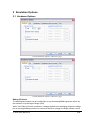
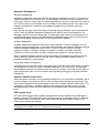
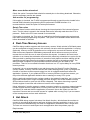
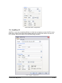
2 Emulation Options
2.1 Hardware Options
iC5000 Emulation Options, Hardware page
iC3000 Emulation Options, Hardware page
Debug I/O levels
The development system can be configured in a way that debug BDM signals are driven by
the emulator or by the target voltage (Vref).
When 'Vref' Debug I/O level is selected, a voltage applied to the belonging reference voltage
pin on the target debug connector is used as a reference voltage for voltage follower, which
iSYSTEM, May 2015
3/35
powers buffers, driving the debug
BDM signals. The user must ensure that the target power supply is connected to the Vref pin
on the target BDM connector and that it is switched on before the debug session is started. If
these two conditions are not meet, it is highly probably that the initial debug connection will
fail already. However in some cases it may succeed but then the system will behave
abnormal.
In case of ic3000 iCARD based development system, emulator firmly drives When a voltage
is selected from the combo box
Sampling threshold levels (iTRACE PRO/GT only)
Sampling threshold level can be set for the CPU trace (output) port. Default Vref/2 setting
should work unless the trace port signals are shifted. In case of problems with the trace
recording, try different voltage levels, e.g. 1.5V, 1.2V, etc.
Hot Attach
Option must be checked when Hot Attach is used. Refer to the Hot Attach chapter for more
details on Hot Attach use.
Note: Hot Attach function cannot be used for any flash programming or code download!
2.2 Initialization Sequence
The user must properly configure the CPU before the debug download (including the flash
programming) can take place to the memory area, which is not accessible upon the CPU
reset. This is essential for the applications using memory resources, for instance external
RAM or external flash, which are not accessible after the CPU reset. In such case, the
debugger executes a so-called initialization sequence immediately after the CPU reset, which
writes to the CPU registers configuring the CPU memory interface to the physical memory
and then the debug download is executed. Note that the initialization sequence must be set
up specific to the application. Besides enabling a disabled memory access upon reset, the
initialization sequence can be used for instance to disable the CPU internal watchdog being
active after reset or to modify any other CPU registers, when it’s preferred to run the
application with the modified CPU reset state. Detailed information may be found in the
Initialization Sequence help topic.
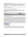
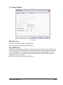
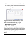
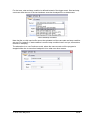
3 CPU Setup
3.1 General Options
The CPU Setup, Options page provides some emulation settings, common to most CPU
families and all emulation modes. Settings that are not valid for currently selected CPU or
emulation mode are disabled. If none of these settings is valid, this page is not shown.
iSYSTEM, May 2015
4/35
General Options
Cache downloaded code only (do not load to target)
When this option is checked, the download files will not propagate to the target using
standard debug download but the Target download files will.
In cases, where the application is previously programmed in the target or it's programmed
through the flash programming dialog, the user may uncheck 'Load code' in the 'Properties'
dialog when specifying the debug download file(s). By doing so, the debugger loads only the
necessary debug information for high level debugging while it doesn't load any code.
However, debug functionalities like the on-chip trace will not work then since an exact code
image of the executed code is required as a prerequisite for the correct trace program flow
reconstruction. This applies also for the call stack on some CPU platforms. In such
applications, 'Load code' option should remain checked and 'Cache downloaded code only
(do not load to target)' option checked instead. This will result in debug information and code
image loaded to the debugger but no memory writes will propagate to the target, which
otherwise normally load the code to the target.
iSYSTEM, May 2015
5/35
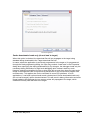
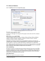
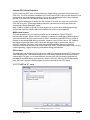
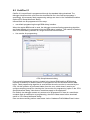
3.2 Debugging options
ColdFire Debugging options (V2, V3, V4, V4e core)
ColdFire Debugging options (V1 core)
iSYSTEM, May 2015
6/35
Execution Breakpoints
Hardware Breakpoints
Hardware breakpoints are breakpoints that are already provided by the CPU. The number of
hardware breakpoints is limited to four. The advantage is that they function anywhere in the
CPU space, which is not the case for software breakpoints, which normally cannot be used in
the FLASH memory, non-writeable memory (ROM) or self-modifying code. If the option 'Use
hardware breakpoints' is selected, only hardware breakpoints are used for execution
breakpoints.
Note that the debugger, when executing source step debug command, uses one breakpoint.
Hence, when all available hardware breakpoints are used as execution breakpoints, the
debugger may fail to execute debug step. The debugger offers 'Reserve one breakpoint for
high-level debugging' option in the Debug/Debug Options/Debugging' tab to circumvent this.
By default this option is checked and the user can uncheck it anytime.
Software Breakpoints
Available hardware breakpoints often prove to be insufficient. Then the debugger can use
unlimited software breakpoints to work around this limitation. Note that the debugger features
unlimited software breakpoints in the CF5211, CF5212, CF5213, CF5214, CF5216,
CF52210, CF52211, CF52212, CF52213, CF52221, CF52223, CF52230, CF52231,
CF52233, CF52234, CF52235, CF5281, CF5282 and ColdFire V1 internal flash too.
When a software breakpoint is being used, the program first attempts to modify the source
code by placing a break instruction into the code. If setting software breakpoint fails, a
hardware breakpoint is used instead.
Using flash software breakpoints
A flash device has a limited number of programming cycles. Belonging flash sector is erased
and programmed every time when a software breakpoint is set or removed. The debugger
sets breakpoints hidden from the user also when a source step is executed. In worst case, a
flash may become worn out due to intense and long lasting debugging using flash software
breakpoints.
Set/clear SW BPs before Run
When the option is checked, then a software breakpoint is not set/cleared immediately, but is
just remembered. Only when the CPU is set to running are the breakpoints committed. This
way several breakpoints can be changed but only one re-FLASH operation takes place. This
is especially noticeable in testIDEA operation with many stubs and also during a regular
debugging session when several breakpoints are set/cleared within the same flash erase
block.
SFR register base
IPS value (SFR register base) used by the application must be entered for the debugger to
be able to display SFRs since IPS value cannot be read by the debugger after it is relocated.
SFR register base is 0x40000000 after reset. Note that this option does not apply for all
CPUs and is disabled accordingly.
Note: This option is not available for ColdFire V1 and also not for all microcontrollers
belonging to the ColdFire V2, V3, V4 and V4e architectures.
iSYSTEM, May 2015
7/35
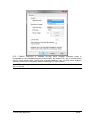
3.3 Reset Options
Reset Options
RESET Duration
The width of the RESET pulse is specified here.
Note: This option is not available for ColdFire V1.
Post RESET Delay
Typically, the on-chip debug module is reset concurrently with the CPU. After the CPU reset
line is released from the active state, the on-chip debug module requires some time (delay)
to become operational. The default delay value normally allows the debugger to gain the
control over the CPU. If a first debug connection fails already try different delay values to
establish the debug connection.
Note: This option is not available for ColdFire V1.
iSYSTEM, May 2015
8/35
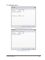
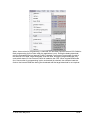
3.4 Advanced Options
3.4.1 ColdFire V2, V3, V4 and V4e core
ColdFire Debugging options (V2, V3, V4, V4e Core)
Override startup register values
If required, the debugger can change the CPU program counter after the CPU is released
from reset.
Allow writes to on-chip FLASH
This option applies only for the CF5211, CF5212, CF5213, CF5214, CF5216, CF52210,
CF52211, CF52212, CF52213, CF52221, CF52223, CF52230, CF52231, CF52233,
CF52234, CF52235, CF5281, CF5282 devices.
If this option is checked, the writes to the on-chip FLASH are allowed. In this case, the
CFMCLKD value, normally used in the target application, must be written in the dialog. Note
that the register is a write-once register and cannot be modified later in the application.
When ‘Mass erase before download’ option is checked, the debugger performs a mass erase
prior to debug download into the internal CPU flash. Note that a mass erase is only possible
when no PROTECT bits (CFMPROT register) are set for that block.
Use handshaking
By default, this option is checked ensuring successful download. Each memory write BDM
command is checked for successful completion. When no handshaking is used, download
speed is increased by up to 3 times. Verify download can be used to verify whether the “no
handshaking” download was successful. If verify errors are reported, revert to the default
settings (the ‘Use handshaking’ option checked).
Ignore Bus Errors
Bus Errors are ignored if this option is checked.
iSYSTEM, May 2015
9/35
Internal CPU Reset Detection
A CPU reset line (RSTI pin) is connected to the target debug connector and is input to the
CPU only. The CPU provides a separate CPU reset output (RSTO pin) but per default it’s not
connected to the target debug connector. Due to this, the debugger has no way to detect
internal CPU reset over the default target debug connection.
In order for the debugger to detect also the internal CPU reset, the user can connect the
CPU RSTO to pin 1 of the target debug connector (otherwise not used) and check the
‘Internal CPU Reset Detection’ option.
Note: ColdFire iCARD (IC30114) must be revision I3 or newer when debugging through
iC3000 and ColdFire iCARD. With older iCARDs this option is not supported.
BDM clock source
This setting applies only for ColdFire iCARD and is disabled for iTRACE PRO/GT
development system. When CLKOUT (default) is selected, the debugger’s BDM engine is
synchronized with the CPU output clock CLKOUT (sometimes named PSTCLK), which is
present on the target BDM debug connector. However, some CPUs runs at 150, 200MHz
and higher frequencies and in such cases the debugger fails to synchronize with the
CLKOUT and then ‘Emulator’ clock must be selected and BDM frequency specified.
Frequency should be less than half of the reset CPU clock. Try different values until you find
a working setting. Higher frequency yields better debug performance.
CPU status
The debugger can recognize CPU status (run, stop) by inspecting the trace PST port or the
CSR debug register. The disadvantage of the CSR debug register is that the status flag is
cleared after it is read. It is recommended to use the trace port (normally connected to a
standard 26-pin BDM debug connector) by default. However, there are CPUs without the
trace PST port, where the debug register must be selected for the CPU status.
3.4.2 ColdFire V1 core
ColdFire Debugging options (V1 Core)
iSYSTEM, May 2015
10/35
Mass erase before download
Check the option if complete flash should be erased prior to the debug download. Otherwise,
only the necessary sectors are erased.
Use monitor for programming
If this option is checked, the FLASH is programmed through a special monitor loaded in the
internal RAM; otherwise programming will be performed via BDM interface. It is
recommended to check the option for better performance.
Retain Trim value
The CPU has a function which allows trimming the internal period of the internal reference
clock. The trim value is stored in the internal flash and is internally read when the CPU is
powered.. Refer to the CPU user manual for more details.
If this option is checked, the Trim value is read before the flash programming and restored
back after the flash programming completes. This option is not available when ‘Mass erase
before download’ is checked.
4 Real-Time Memory Access
ColdFire debug module supports real-time memory access. Watch window’s Rt.Watch panes
can be configured to inspect memory with minimum intrusion while the application is running.
Optionally, memory and SFR windows can be configured to use real-time access as well.
Real-time access operation: BDM debug commands which reference memory must first
request the bus from the core in order to perform the access. Included in this concurrent
operation is an internal bus arbitration scheme which effectively schedules bus cycles for the
debug module by stalling the processor´s instruction fetch pipeline and then waiting until all
operand requests have been serviced before granting the bus to the debug module. The
debug module completes one bus transaction before releasing the bus back to the
processor. There is an unverified information that there is a 4..6 cycles delay for every BDM
memory access.
In general it is not recommended to use real-time access for Special Function Registers
(SFRs) window. In reality, real-time access still means stealing some cycles. As long as the
number of real-time access requests stays low, this is negligible and doesn't affect the
application. However, if you update all SFRs or memory window via real-time access, you
may notice different application behavior due to stealing too many CPU cycles.
When a particular special function register needs to be updated in real-time, put it in the realtime watch window (don't forget to enable real-time access in the SFRs window but keep
SFRs window closed or open but with SFRs collapsed). This allows observing a special
function register in real-time with minimum intrusion on the application.
Using “alternative” monitor access to update a memory location or a memory mapped special
function register while the application is running works like this: the application is stopped,
the memory is read and then the application is resumed. Hence the impact on real time
execution is severe and use monitor access for 'update while running' only if you are aware
of the consequences and can work with them.
5 Hot Attach
ColdFire BDM debug support includes a Hot Attach function, which allows the emulator to
connect to a working target device and have all debug functions available. As such, it is a
very convenient troubleshooting tool when the application misbehaves after a longer time.
The user can connect to and inspect such an application after the problem pops-up.
Requirements:
iSYSTEM, May 2015
11/35
1K ohm pull-down must be added on the DSCLK (BDM clock) CPU pin, which keeps the
DSCLK pin at low level while the debugger is not connected to the target.
To hot attach to a running target with no debugger connected:
Check the ‘Hot attach to target’ option in the ‘Hardware/Emulation Options/Hardware’ tab.
Execute Download debug command.
Connect the BDM cable to the target system
Select the 'Attach' debug command in the ‘Debug’ menu to attach to the target system.
Now, the debugger should display run status and the application can be stopped and
debugged.
Select 'Detach' debug command in the ‘Debug’ menu to disconnect from the target
application. If the CPU was stopped before detach, it will be set to running.
Note: Hot Attach function cannot be used for any flash programming or code download!
6 Internal FLASH programming
6.1 ColdFire V2, V3, V4 and V4e core
Internal CPU flash programming directly through the debug download is supported on
CF5211, CF5212, CF5213, CF5214, CF5216, CF52210, CF52211, CF52212, CF52213,
CF52221, CF52223, CF52230, CF52231, CF52233, CF52234, CF52235, CF52252(C),
CF52254(C), CF52255C, CF52256(C), CF52258(C), CF52259C, CF5281, CF5282 (check
with iSYSTEM for the latest list) and devices based on ColdFire V1 core. Software
breakpoints in the flash and flash modification through the memory window are supported
too. Flash is modified by loading a small flash programming monitor into the internal CPU
RAM, where it’s then executed. Complete operation is hidden to the user and does not
restrict any available CPU resource for the application.
In order to download the code into the internal flash, the user must (does not apply for
ColdFire V1):
iSYSTEM, May 2015
12/35
Configure the FLASHBAR register using winIDEA initialization sequence unless the
internal flash is already visible and enabled at the correct address after the CPU reset. It
is recommended that the FLASHBAR register value from the application is used or a
conflict will occur when flash modification is required while debugging the application.
Flash is modified when using software breakpoints or modifying its content in the memory
window.
Configure the RAMBAR register using winIDEA initialization sequence unless the internal
RAM is already visible and enabled at the correct address after the CPU reset. It is
recommended that the RAMBAR register value from the application is used or a conflict
will occur when flash modification is required while debugging the application. Flash is
modified when using software breakpoints or modifying its content in the memory
window.
Check the ‘Allow writes to on-chip FLASH’ option in the ‘CPU setup/Advanced’ tab.
Calculate and enter the CFMCLKD register value in the ‘CPU setup/Advanced’ tab
depending on the target CPU clock.
Double check that the CFMCLKD value matches with the target CPU clock during the
debug download when the flash is being programmed. To issue any flash command,
CFMCLKD register must be written to divide the flash input clock to within 150kHz and
200kHz range. Setting CFMCLKD to a value such that FCLK < 150kHz can destroy the
flash memory due to overstress. Setting CFMCLKD to a value such that FCLK > 200kH
can result in incomplete programming or erasure of the flash memory array cells.
Configure the CFMPROT register (sector protection) register using winIDEA initialization
unless the necessary flash logical sectors are already not protected after the CPU reset.
Flash programming may fail when any of the above settings is not done or is
configured improperly.
Refer to the CPU datasheet for more details on the ColdFire Flash Module (CFM)
configuration.
The FLASH programming is executed automatically during the debug download and hidden
from the user.
Maximum FLASH programming speed is achieved by unchecking ‘Use handshaking’ option
in the ‘Hardware/Emulation Options/CPU Setup/Advanced’ tab but it may not work always.
Note: CFMDACC register must be configured properly to be able to run the code from the
internal flash. By default the flash is mapped into the data address space. Refer to
Microcontroller Reference Manual for more details on CFMDACC register.
Unsecure flash
Flash security can be enabled through the CFM Security register (CFMSEC). Enabling flash
security disables BDM debug communication, which also means that the debug connection
can no longer be established. Security protection can be removed only through the JTAG
interface by erasing the entire CPU flash.
During BDM debug session, JTAG_EN pin is tied to low and CPU PSTCLK/TCLK pin is
connected to pin 24 of the target debug connector. To unsecure the flash, the target must be
reconfigured for the JTAG operation. JTAG_EN pin must be tied to high and CPU
PSTCLK/TCLK pin must be connected to pin 6 of the target debug connector. Refer to the
Microcontroller Reference Manual for more details. After a complete system including the
debug tool is powered up, press the Hardware/Flash->Unsecure button. This operation takes
approximately 40s. When it’s done, reconfigure the target back for the BDM operation and
new debug session can be started.
iSYSTEM, May 2015
13/35
6.2 ColdFire V1
Coldfire V1 internal flash is programmed through the standard debug download. The
debugger identifies which code from the download file fits in the flash and programs it
accordingly. All necessary flash programming settings are done in the ‘Hardware/Emulation
Options/CPU Setup/Advanced’ dialog.
Internal flash can be programmed in two ways:
use default programming through BDM debug interface
When the regular BDM mode is used, the debugger executes flash programming algorithm
and feeds the data to be programmed via the BDM debug interface. This method is relatively
slow since BDM debug interface is a single wire serial communication.
Use monitor for programming
CPU Setup/Advanced dialog
First a small programming monitor is loaded in the internal RAM and then BDM debug
interface is used only to feed the data to be programmed into the allocated monitor data
buffer. Flash programming algorithm is executed fast since the monitor is executed by the
CPU. All this operation is performed hidden from the user, which doesn’t need to preconfigure anything except for checking the ‘Use monitor for programming’ option in the ‘CPU
Setup/Advanced’ dialog. Note that no restrictions apply to the application.
Per default, the debugger erases only sectors to be programmed. If there is a need that a
complete flash is erased prior to programming, check the ‘Mass erase before download’
option in ‘CPU Setup/Advanced’ dialog.
User can also manually perform mass erase via the ‘Hardware/FLASH/Mass Erase’ button.
iSYSTEM, May 2015
14/35
When ‘Use monitor for programming’ is selected, the emulator requires internal CPU RAM for
flash programming (but not later when the application is run). During the debug download,
only the code which fits into internal FLASH is loaded. If you want to load a part of code to
the internal CPU RAM, ‘target download’ must be used. During the target download, only
code which doesn’t fit into internal FLASH is loaded to the CPU. When regular BDM mode
(the ‘Use monitor for programming’ option unchecked) is selected, the emulator loads the
code to the internal RAM also during the download and the target download is not required.
iSYSTEM, May 2015
15/35
7 Access Breakpoints and Trace Trigger
Access breakpoints and on-chip trace trigger share the same on-chip debug resources,
which means that the same CPU event can be either configured for access breakpoint or
trace trigger. Consequentially, trace and access breakpoints cannot be used at the same
time.
7.1 ColdFire V2, V3, V4 and V4e core
In the Rev. A debug module, certain hardware structures are shared between BDM and
breakpoint/trigger functionality. Loading a register to perform a specific function that shares
hardware resources is destructive to the shared function. For example, a BDM command to
access memory overwrites an address breakpoint/trigger. This means that the user must
not use real-time access (RT watch pane) while using access breakpoints or trace
trigger! Double check that ‘Update when running’ option is disabled for real-time
access while using trace! Rev. B, B+, C and D debug modules do not have this restriction.
Depending on the integrated debug module revision, there are two types of breakpoint/trace
configuration dialogs, and not all options are enabled on all CPUs, depending on the on-chip
resources available for the selected CPU.
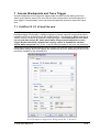
Access Breakpoint Configuration: Debug module Rev. A, B and B+
iSYSTEM, May 2015
16/35
For CPUs featuring Rev. A, B and B+ debug module, Access Breakpoint / Trigger can be
configured as 1 or 2-level logical combination of PC (execution address), Address (address
being accessed) and Data (data being accessed).
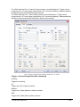
For CPUs featuring Rev. C and D debug module, Access Breakpoint / Trigger can be
configured as 1 or 2-level logical combination of PC (execution address), Address/Address1
(address being accessed) and Data/Data1 (data being accessed).
Trace Trigger Configuration: Debug module Rev. C and D
Trigger / Access Breakpoint mode combining
Anything
Triggers on anything
PC
Trigger when PC condition matches.
Address
Trigger when (Data) Address condition matches
Data
Trigger when (Data) Data condition matches.
iSYSTEM, May 2015
17/35
Address and Data
Trigger when configured address, data and access type match within the same bus cycle.
PC OR Address
Trigger when PC is reached or (Data) Address condition is matched within the same bus
cycle.
PC OR (Address AND Data)
Trigger when PC is reached or (Data) Address and (Data) Data conditions are matched
within the same bus cycle.
PC THEN Address
Trigger when first PC is reached and then (Data) Address condition is matched.
PC THEN Data
Trigger when first PC is reached and then (Data) Data condition is matched.
PC THEN (Address AND Data)
Trigger when first PC is reached and then (Data) Address and (Data) Data conditions are
matched.
Address THEN PC
Trigger when first the (Data) Address condition is matched and then PC is reached.
Data THEN PC
Trigger when first the (Data) Data condition is matched and then PC is reached.
(Address AND Data) THEN PC
Trigger when first both the (Data) Address and (Data) Data conditions are reached and then
PC is reached.
Extended configuration options
The extended configuration options of Rev. C and Rev. D on-chip debug resource logic
implements additional options to configure breakpoint and trigger events. The improved
resources include Address1 and Data1 conditions and consequently there are more
combinations of the conditions available.
iSYSTEM, May 2015
18/35
Recorder (Trace)
Start
Depending on the setting the Trace can start recording immediately or on trigger or trace can
be configured for a so called Continuous Mode.
Typical use case is start trace recording on a trigger event where focus is around the
configured trigger event. Alternatively the trace can be configured to stop recording on a
program stop where focus is on program just before application stop. ‘Continuous mode’ use
allows roll over of the trace buffer, which results in the trace recording up to the moment
when the application stops. In practice, the trace displays the program flow just before the
program stops. For instance, due to the breakpoint hit, due to the stop debug command
issued by the user or due to the erratic state of the CPU which initiated the application stop.
Buffer Size
Choose desired buffer size. Primarily trace capture time depends on this setting and later on
trace upload time as well.
Trigger Position
Depending on the needs, trigger can be located at the beginning (located at 1/64th of the
trace buffer), in the center (located in the middle of the trace buffer) or at the end of the trace
buffer (located at 63/64th of the trace buffer). Note that the trigger position may not
configurable for minimum buffer. If the user intends to analyze the trace record after the
trigger, it makes sense to use ‘Begin’ trigger position and ‘End’ trigger position when the
trace pre-history that is program behavior before trigger is required.
iSYSTEM, May 2015
19/35
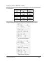
Configuring ‘Address AND Data’ condition
Below table shows relationships between processor address, access size, and location within
the 32-bit data bus.
A[1:0]
Access Size
00
Byte
Operand
Location
D[31:24]
01
Byte
D[23:16]
10
Byte
D[15:8]
11
Byte
D[7:0]
0x
Word
D[31:16]
1x
Word
D[15:0]
xx
Longword
D{31:0]
When configuring trigger or access breakpoint on a data with specific data value, the
debugger considers above table and configures on-chip debug resource accordingly.
8-bit data value configuration
16-bit data value configuration
iSYSTEM, May 2015
20/35
32-bit data value configuration
7.2 ColdFire V1
ColdFire V1 core has completely different on-chip trace comparing to other ColdFire cores.
First of all, it has on-chip trace buffer and no trace port. On chip trace buffer can store 64
PST records, which are read out via the BDM debug interface.
Trace Trigger configuration
iSYSTEM, May 2015
21/35
For the trace, start and stop condition is defined instead of the trigger event. Start and stop
event can either be one of the two hardware execution breakpoints or a data access.
Trace Start/Stop condition
Note that the on-chip trace buffer cannot be uploaded until the trace start and stop condition
are met. For instance, if start condition is met but stop condition hasn’t met yet, trace status
remains in sampling.
The alternative is to use Continous mode, where the trace records until the program is
stopped either due to execution breakpoint hit or what ever other reason.
iSYSTEM, May 2015
22/35
8 Trace
ColdFire CPUs feature real-time trace, which allows the user insight into the program
execution flow. The trace port is not available on all ColdFire devices. Typically, devices in
small pin-count package don’t have the trace port.
The ColdFire debug architecture ((V2, V3, V4, V4e core) implements an 8-bit parallel output
bus that reports processor execution status and data to an external emulator system, which
records the trace information in the trace buffer. Note that the processor status may not be
related to the current bus transfer.
Devices based on ColdFire V1 core have no trace port, but there is limited on-chip trace
buffer, which is read via debug interface.
External development system can use the trace output stream with an external image of the
program to completely track the dynamic execution path. An accurate code image (download
file) is a precondition for correct execution path reconstruction. This tracking is complicated
by any change in flow, especially when branch target address calculation is based on the
contents of a program-visible register. Trace outputs can be configured to display the target
address of such instructions in sequential nibble increments across multiple processor clock
cycles.
Rev. A, B and B+ debug module
Two 32-bit storage elements form a FIFO buffer connecting the processor’s high-speed
local bus to the external development system through PST[3:0] and DDATA[3:0] trace
port. Execution speed is affected only when both storage elements contain valid data to
be dumped to the trace output. The core stalls until one FIFO entry is available.
Rev. C and D debug module
Four 32-bit storage elements form a FIFO buffer connecting the processor’s high-speed
local bus to the external development system through PSTDDATA[7:0] trace port.
Execution speed is affected only when three storage elements contain valid data to be
dumped to the trace output. This occurs only when two values are captured
simultaneously in a read-modify-write operation. The core stalls until two FIFO entries are
available.
ColdFire V1 devices implements on-chip trace buffer that records processor execution status
and data, which can be subsequently accessed by the external emulator hardware to provide
program (and optional partial data) trace information. On-chip trace buffer provides
programmable start/stop recording conditions.
The option ‘Break on trigger’ should not be used on ColdFire (except on V1 core). If the
option is used, last part of the program executed prior to the trigger event is not displayed in
the trace window. “Missing” program part cannot be reconstructed because the CPU stops
sending the trace information as soon as the CPU is stopped even though there is still trace
information to be sent out from the internal trace FIFOs. Note also that there is latency
between the CPU bus transfer and belonging trace output information.
Real-Time Compression (RTC)
iC5000 and iC3000 based iTRACE GT development system feature a unique compression
technology, which compresses the trace information captured on the microcontroller trace
port before it’s stored in the trace storage buffer. RTC allows capturing longer trace session
with the same physical trace buffer comparing to the standard ColdFire on-chip trace.
iSYSTEM, May 2015
23/35
RTC (‘iTRACE’ selection) or standard ‘On-chip trace’ analyzer operation mode is
configurable in the Hardware/Analyzer Setup dialog. By default RTC use is recommended
since it yields longer trace, profiler and coverage sessions. Use ‘On-Chip trace’ analyzer
operation mode for co-verification when questioning RTC trace results.
Note: RTC technology is supported only on ColdFire microcontrollers featuring debug module
Rev. A, B or B+.
iSYSTEM, May 2015
24/35
ColdFire V2 Trace Examples
Example 1: Trace triggers on a function Type_Pointers. Using trace, the program flow
before the trigger event and after the trigger event can be inspected.
This is a very often used scenario. Trace triggers on a specific function or source line and the
user can inspect the program execution before and after the trigger event.
Set the Recorder to start ‘On Trigger’ and set the trigger position to ‘Center’.
On the Trigger page select ‘PC’ condition in the ‘Combining’ field and select
Type_Pointers function by pressing button on the right which invokes ‘Symbol Browser’.
Now, execute CPU reset, start trace and run the program. After Type_Pointers is
executed for the first time, trace window displays program flow before and after the entry to
the function.
iSYSTEM, May 2015
25/35
Example 2: The user gets incorrect writes to a particular address/variable. Example 2
demonstrates how to locate the code writing faulty value (0xC020) to a global variable
iCounter.
Set the Recorder to start ‘On Trigger’ and set Trigger Position to ‘Center’.
On the Trigger page select ‘Address AND Data’ condition in the ‘Combining’ field and select
iCounter variable by pressing button on the right which invokes ‘Symbol Browser’. Next,
set ‘Write’ for the access type and finally enter data value 0xC020.
iSYSTEM, May 2015
26/35
Let’s define a qualifier now. In our case, the trace should additionally capture data read and
write for operands. By default Qualifier is set to ‘None’, which results in trace recording
instructions only.
Execute CPU reset, start the trace and run the program. When faulty write occurs, a trace
trigger event occurs simultaneously. The trace buffer fills up and the program flow is
reconstructed and displayed. Since pre-trigger history is visible, the user can easily locate the
code writing 0xC020 to the iInterruptCounter variable and fix the problem. There is
always some misalignment between the actual trigger event and the one depicted in the
trace window (frame 0) due to the nature of the on-chip trace. In this particular case,
instruction which generated the trigger event, holds marker -26.0.
iSYSTEM, May 2015
27/35
9 Profiler
Refer to winIDEA Contents Help, Profiler Concepts section for Profiler theory and
background.
Refer to winIDEA Contents Help, Analyzer Window section (or alternatively to the standalone
Analyzer.pdf document) for information on Profiler user interface and use.
Coldfire V1 doesn’t feature profiler since the trace doesn’t provide time stamp information
Data profiler can be used on WDDATA instruction only. The operand data trace does not
provide the required information for the usual data profiler use.
10 Coverage
Refer to winIDEA Contents Help, Coverage Concepts section for Coverage theory and
background.
Refer to winIDEA Contents Help, Analyzer Window section (or alternatively to the standalone
Analyzer.pdf document) for information on Coverage user interface and use.
In general it makes no sense using coverage on Coldfire V1, where only up to few thousands
of program instructions can be recorded in the best case (depends on the application code).
However it can still be used if coverage is required to be performed on a particular function or
code section only.
iSYSTEM, May 2015
28/35
11 Emulation Notes
Most of ColdFire CF52xx CPUs feature the Revision A enhanced hardware debug
support while there are new CF52xx CPUs, which feature the Revision B/B+ enhanced
hardware debug support. ColdFire CF54xx feature the Revision D enhanced hardware
debug support. Since there is different debugging behavior between them, the user
should check specific Reference Manual (Debug Module chapter) in order to determine
the Revision of enhanced hardware debug support that is in his specific CPU.
In the Revision A implementation of the debug module, certain hardware structures are
shared between BDM and breakpoint functionality.
Register
ABHR
BDM Function
Bus attributes for all memory
commands
Address for all memory commands
Breakpoint Function
Attributes for address
breakpoint
Address for address
DBR
Data for all BDM write commands
breakpoint
Data for data breakpoint
AATR
Rev. A Shared BDM/Breakpoint Hardware
Thus, loading a register to perform a specific function that shares hardware resources is
destructive to the shared function. For example, a BDM command to access memory
overwrites an address breakpoint in ABHR. A BDM write command overwrites the data
breakpoint in DBR.
All above facts are important during debug support implementation but at the end they
impact the user when debugging his application. When CPU has Rev. A debug module,
the user must not use access breakpoints nor trace trigger together with any memory
referencing debug functionalities. Thereby, make sure that access breakpoints and trace
trigger are not active (disabled) when using real-time watches, setting software
breakpoints, modifying and reading memory, etc. In order to use access breakpoints or
trace trigger, disable real-time access and use one available hardware execution
breakpoint.
ColdFire data trace is noticeably different from other on-chip Nexus based trace
implementations supporting data trace. ColdFire trace was one of the first on-chip trace
solutions and was implemented quite some time before Nexus standard was defined,
which is widely adopted by silicon vendors in last few years.
ColdFire debug module provides a bit, which controls operand data capture for
PSTDDATA (trace port). The user can opt for no operand data capture, capture all write
data, capture all read data and capture all read/write data.
Let's first take a look how a data record looks in a Nexus based on-chip trace available
for instance on Freescale MPC5500 family. The trace window shows concrete memory
read and memory write access to the memory. For instance, frame 213 shows 32-bit
memory write of value 0x00000004 to address 0x40002014.
iSYSTEM, May 2015
29/35
MPC5500 Nexus trace record
Now, let’s see the ColdFire trace record for a similar code, which reads 0x3 from 32-bit
iCounter variable, increments it and writes back the new value (0x4).
ColdFire CF5235 trace record
First of all, ColdFire trace displays operand data and not concrete memory read or write
access. In this particular case, two data cycles, depicted as frame -23.2 and -23.3,
belong to ADD.L D0, (0x0010024).L
assembler instruction and not to the particular memory access. Chapter Debug Module in
the CPU Reference Manual precisely describes what kind of operand data can each
assembler instruction generate. In our example, first operand data (frame -23.2)
represent source for the instruction and second operand data destination. Trace record
does not directly show the address of the variable, which the application reads first and
then writes to.
Starting the trace while the CPU is already running
In case of ColdFire CF52xx CPUs, the data trace must not be used in order for the
debugger to be able to synchronize program trace with the current CPU program counter.
ColdFire CF54xx CPUs have slightly modified trace implementation in the debug module
comparing to CF52xx due to higher CPU frequencies. Due to these modifications, the
debugger cannot synchronize program trace with current program counter even when the
data trace is disabled. Hence, the trace needs to be started before program run while the
iSYSTEM, May 2015
30/35
CPU is in stop. Only in this case the debugger can always synchronize properly program
trace with actual program execution.
Trace Trigger
ColdFire CF54xx trace implementation does not allow reliable hardware detection of the
trigger event. The CPU transmits extra coding on the trace port for the trigger event but
the same coding can be generated as part of a trace message indicating a change in
program flow. Consequentially, when using trace trigger, the trigger marker more often
than not points to an incorrect location in the trace record. Thereby, it is recommended to
use the trace in ‘Record everything’ mode instead in ‘Trigger’ mode.
Interrupts
It is not allowed to perform source step over the code, which modifies the interrupt level
mask in the core SR register. Such step would yield wrong SR register value since
interrupts are disabled (interrupt level raised to maximum) before every source step.
Interrupts are disabled by the debugger to have a more predictable debugging of
applications using interrupts. For instance, if there is a periodic interrupt and interrupts
would not be disabled during the source step, the user would keep entering the interrupt
routine while stepping.
Watchdog
It is recommended to disable any internal or external watchdog to prevent conflicts with
the debugger. Per default, the debugger cannot detect any internal watchdog reset and
will lose the control over the CPU in case of internal CPU reset. Refer to Internal CPU
Reset detection chapter for more details on this option.
12 Getting Started
1) Connect the system
2) Make sure that the target debug connector pinout matches with the one requested by
a debug tool. If it doesn't, make the necessary adaptation to comply with the standard
connector otherwise the target or the debug tool may be damaged.
3) Power up the emulator and then power up the target.
4) Execute debug reset
5) The CPU should stop on the reset location.
6) Enable internal CPU RAM by manually initializing belonging CPU register (RAMBAR).
7) Open memory window at internal CPU RAM location and check whether you are able
to modify its content.
8) If you passed all 7 steps successfully, the debugger is operational. Now you may add
the download file and load the code to the RAM. Read the ‘Internal FLASH
Programming’ chapter before downloading the code in the CPUs with the internal
flash memory.
9) To program the external flash or download the code to the external RAM, which is not
accessible after reset, make sure you use the initialization sequence to enable the
access. First, the debugger executes reset, then the initialization sequence and finally
the download or flash programming is carried out.
13 Troubleshooting
I’m programming the code in the external flash. The flash is programmed correctly but
after the download completes, I see bad content in the memory window. I get correct
iSYSTEM, May 2015
31/35
content again if I perform a debug reset afterwards. What’s wrong?
Check the 'Cache downloaded code only (do not load to the target)' option on the
'Hardware/Emulation Options/CPU Setup/Options' tab. With current configuration, the
debugger performs additional memory writes into the flash area (as part of the debug
download) after the flash is being programming already. This seems to conflict with the
CPU and yields bad starting point. With the above option checked, memory writes
belonging to the debug download do not propagate to the target flash. However, be
careful not to use this option if you are trying to download something into the RAM. Refer
to Advanced Options chapter for more details on this option.
In case of problems with flash programming, double check that the CFMCLKD value
matches with the target CPU clock during the debug download when the flash is being
programmed. Refer to the Internal Flash Programming chapter covering the flash
programming and to CPU reference manual for more details on the CFMCLKD register.
In case of any problems with the program flow in the trace or with profiler operation or
with coverage operation, double check the settings in the ‘Hardware/Analyze
Setup/ColdFire’ tab where trace branch target address is configured.
When I trace my program I get nothing displayed in the trace window. What’s wrong?
First of all make sure that the program image is provided to the debugger via the
download file. Otherwise the trace cannot reconstruct the program. This could be an
issue if the code would be run for instance from the preprogrammed external flash. Next,
the “problem” may also come from the program. The debugger reads physical trace
memory in blocks and can read block from any location in the trace buffer depending on
the position of the scroll bar in the trace window. Sometimes it can happen that such
block has no indirect branch message recorded, which reports the debugger the program
counter from which point on a program reconstruction can start in the trace. This can
easily happen with a long program loop or an idle loop waiting for an interrupt. Such code
may not report any program counter information on the trace port but generate sequential
instruction information only. Try to shorten the loop or remove such the code for the test
and see if that’s the problem.
When Error 176 pops up, try to increase the post reset delay.
Make sure that the power supply is applied to the target BDM connector when ‘Vref’ is
selected for ‘Debug I/O levels’ in the ‘Hardware/Emulator Options/Hardware’ tab,
otherwise emulation fails or may behave unpredictably.
When initial debug connection fails, make sure that there is no capacitor on the reset line.
If there is an external reset circuitry, it is recommended to temporarily disable/disconnect
it while troubleshooting the initial debug connection.
Try different setting for debug I/O levels (‘Hardware/Emulator Options/Hardware’ tab) in
case of startup problems when debugging with ColdFire iCARD.
When the debugger addresses reserved IPSBAR memory space, it will yield an
unterminated bus cycle that causes the core to hang. Only a hard reset will allow the core
to recover. This can easily happen when for instance Variable window is open during the
iSYSTEM, May 2015
32/35
debug session and an uninitialized pointer points to the reserved IPSBAR space. For
example, on CF5213, IPSBAR window starts at 0x4000 0000 after reset and covers 1GB
memory space. Special function registers are allocated at the begging of the window.
Accessing area with no mapped registers (e.g. address 0xFFFF4000) will hang the core.
To avoid this, it is recommended to block read accesses into this area by using the
‘Debug/Debug Options/Memory Regions’ dialog. For this particular case, blocking
accesses into the 0x4500 000 – 0xFFFF FFFF memory range, would solve the problem.
Make sure you don’t block accesses into the special function registers accidentally. Note
also that the IPSBAR space can be moved by the application through the IPSBAR
register.
External flash programming CF5407, CF5470, CF5471, CF5472, CF5473, CF5474,
CF5475: Flash programming monitor must not be allocated in the internal SRAM. On
these CPUs, internal SRAM is either only connected to the instruction bus or data bus,
depending on the setting in the RAMBAR register. This means that the monitor cannot be
executed from the SRAM and at the same moment being able to write into the SRAM
(monitor data buffer).
When performing any kind of checksum, remove all software breakpoints since they may
impact the checksum result.
When the trace content doesn’t seem to match with the executed code:
o
Check if correct Sampling and debug threshold levels are set in the
‘Hardware/Emulation Options/Hardware’ tab.
o
Make sure that the ‘Entire 4 bytes’ option is set for the Branch target address in the
‘Hardware/Analyzer Setup/ColdFire’ tab.
o
Make sure that the image of the executed code is downloaded to the debugger since
the trace reconstruction is based on it.
In case of ColdFire V1 devices, it is possible to use data access address & data value for
on-chip trace start/stop condition. However, data value does not work for on-chip trace
while it works fine when configured for access breakpoint.
MCF5282 errata V2.0 (check the latest errata if the issue is fixed): The V2 core used in
MCF5282 adds support for separate user and supervisor stack pointers. The hardware
implements an active stack pointer and an “other_stack_pointer”. Whenever the
operating mode of the processor changes (supervisor->user, user->supervisor), the
processor hardware “exchanges” the active SP and the other SP.
This exchange operation does not work when the processor mode is changed by a write
to the SR from the BDM port. The hardware in the processor core required to process the
BDM load_SR operation and enable the stack pointer exchange is missing. The
exchange works properly when the SR is changed through software.
Workaround: Use software for any operations that require exchanging the stack pointers.
Q: I download the file, which is in Elf/dwarf format. I don’t get any verify errors. However,
the code doesn’t run. It seems like not all code was really loaded. What could be the
problem?
A: In your particular case, 'Load Code from' in the winIDEA Elf/Dwarf Options dialog (click
Properties after specifying the download file) is set to Program Header / Virtual.
As usual, the choice between virtual and physical addresses is compiler and linker
configuration dependant. If 'not all code is loaded', the following procedure is advisable:
1. generate map file
2. in winIDEA, Elf properties, select 'Dump Elf header'
3. Compare map file to the PROGRAM HEADERS entries for VIRTADDR and PHYADDR
and see which is suitable
iSYSTEM, May 2015
33/35
In this particular case the PROGRAM HEADERS part looks like this:
===============
PROGRAM HEADERS
================
NUM TYPE
OFFSET
0 LOAD
174
1 LOAD
474
2 LOAD
174
3 LOAD
48C
4 LOAD
174
5 LOAD
174
6 LOAD
BB0
7 LOAD
BB4
8 LOAD
BB4
9 LOAD
BB4
SIZE
300
18
0
724
0
0
4
0
0
18
VIRTADDR
0
400
500
500
20000000
20000400
20000400
20000404
20000520
20000520
PHYADDR
0
400
500
500
20000000
20000400
C24
20000404
20000520
C28
MEMSIZE
300
18
0
724
0
0
4
11C
0
18
FLAGS
5
5
5
5
7
7
7
7
7
7
ALIGNMNT
4
4
4
4
4
4
4
4
4
4
As you (should) know, a C/C++ application must initialize global data before entering main.
The initialized data segment is copied from ROM to RAM, uninitialized (.bss) is simply
zeroed.
On your specific CPU, ROM/FLASH resides on address 0, while RAM resides on address
20000000h. The program headers layout shows a few entries where PHYADDR is different
to VIRTADDR. It is obvious that in this configuration the PHYADDR denotes the FLASH load
location and VIRTADDR the link location (the address of RAM where variables will be
accessed). Since apparently the application is PROMable (i.e. startup code will copy .initdata
to .data), we must ensure that the FLASH is loaded with initialized data image and the
correct choice is to select "Program Header / Physical"
Note that on average in 70%of cases Program Header / Virtual is the right choice, so
winIDEA uses this setting per default.
iSYSTEM, May 2015
34/35
Disclaimer: iSYSTEM assumes no responsibility for any errors which may appear in this
document, reserves the right to change devices or specifications detailed herein at any time
without notice, and does not make any commitment to update the information herein.
iSYSTEM. All rights reserved.
iSYSTEM, May 2015
35/35