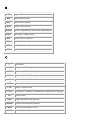
1
Choosing Components: Part 1
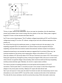
INTRODUCTION
Electronic components are specified by their parameters. A parameter is some property of the component that
has a numerical value, and describes one feature of the component's performance. The values of a given
component's parameters are found in the manufacturer's data sheet and are usually called the "specs"
(specifications).
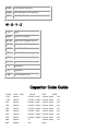
For instance, the following is a partial list of specs for a resistor:
tolerance: 5%, 1%, 0.1%, etc.
wattage: 1/4 W, 1/2 W, 1 W, etc.
material: carbon film, metal film, wire-wound, etc.
temperature range: commercial (0 to 70 degrees C), military (-55 to 125 degrees C) , etc.
temperature coefficient (tempco): given as percent/degree or ppm/degree
physical dimensions: length, diameter, etc.
form-factor: axial leads, radial leads, etc.
MTBF (mean-time-before-failure): hours
price: always a consideration
If something as simple as a resistor has that many specs, you can imagine how many a transistor or
integrated circuit must have. The obvious question is: How do you choose a part? The answer is twofold. First, know what specs a component has. Second, know which specs are important for your
application.
The first part, knowing what specs a component has, is the easy one. For something as common as a
resistor, you can find the information in an introductory text book. For any component, the best source
of information is the manufacturer's data sheet. It used to be that you had to get the data sheets as
hard-copy, often in the form of a data book. Now you can almost always go to a manufacturer's WEB
site and download the data sheets.
It's the second part, knowing which specs are important for your application, that takes some
analysis. A good source for this purpose are the application notes (ap-notes) that most component
manufacturers supply, and which also can be found at the WEB site.
WHAT IS IMPORTANT
How do you know what's important? The answer is to understand what it is you're trying to do. If you
understand what role a component plays in your design, you can identify most of the key parameters
immediately. A few may not be obvious, but can usually be recognized when you test your
breadboard.
For example, suppose you are building a "quick and dirty" 5-Volt power supply to use on your bench,
and it uses an LED to indicate when it is on. You need to choose a resistor to limit the current in the
LED. So what specs are important for that resistor? Well, certainly the value and wattage are
important. But since you just want to see whether the LED is on or off, the tolerance of the resistor is
not going to be critical. The worst tolerance you can find on a resistor is 20%, and that would be
adequate. So a common 5% resistor will work fine.
Let's look at some of the other resistor specs:
Material: since this is not a demanding application for a resistor, choose the most common, and lowest
cost, device. That would be carbon film.
Temperature Range: the supply is going to be on your bench, not in a tank. So you don't need a
military temperature range, the commercial range is sufficient.
Tempco: since the tolerance wasn't important in this application, then the drift in value due to
temperature won't be an issue since it will have less impact than the tolerance.
Physical Dimensions: once you have chosen the material, the size is mostly determined by the power
rating.
Form-factor: again, choose the most common, lowest cost, version: axial leads.
MTBF: not a concern in this application. If the proper wattage is used, even common resistors are very
reliable.
Some parameters, such as size and wattage, are interrelated. Higher wattage resistors are going to
be physically bigger than lower wattage resistors of the same type. But a 2 Watt wire-wound resistor
may be smaller than a 1 Watt carbon film resistor. Also, the dimensions of a 100 Ohm, 1/2 Watt
carbon resistor will depend on whether it has radial leads or axial leads, or is a surface mounted
device with no leads.
Some parameters depend on production considerations. We said to use a resistor with axial leads for
that LED. The assumption was that your design was for a "one-off" project you're building by hand. If
you were designing a commercial product for high-speed, high-volume production, then you would
use a surface mount device. Why? Because high-speed, high-volume production is done by
machines which can use surface-mount components more efficiently.
IDENTIFYING KEY PARAMETERS
The first step in choosing a device is to decide which parameters are crucial and which parameters
are not. For the resistor example above, wattage was crucial but tolerance was not. We decided that
by knowing what role that resistor had to play in the design. Now let's look at something more
complicated than a resistor for an LED. Let's look at a bipolar junction transistor (BJT). If you have an
Adobe reader, you can see a typical transistor data sheet at:
To be able to view this document, your free copy of Acrobat Reader software from the Adobe site.
Of all the parameters on a transistor data sheet, how do you identify the key parameters for your
application? You do it by analyzing two things: first, what does this transistor do in the design, and
second, what parameters relate to that job. While you know the role you want the transistor to play,
components sometimes interact in ways that we didn't anticipate. So it is necessary to analyze just
what the transistor is actually doing.
As for knowing how the specs relate to performance, look for those parameters that are expressed in
the same terms, or units of measure, as the key role of the transistor. Start with the obvious things:
the maximums for voltage, current, and power. Then move on to other parameters that are crucial to
the application.
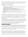
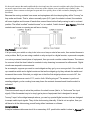
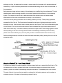
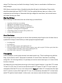
For example, suppose you want to use a transistor as a switch: either on or off (see Figure 1). When
it is on, the transistor will conduct the most current through its collector. So you need to look at the
spec for maximum collector current ( MAX IC ) which will be in Amps or milliAmps. When it is off, the
transistor will have the maximum voltage at the collector. So you need to look at the spec for
maximum collector voltage, sometimes called 'breakdown' voltage. You will find two maximum
voltage specs on the data sheet: one for collector-to-emitter ( VCE or VCEO ) and one for collectorto-base ( VCB or VCBO ). Use the lesser of the two values.
Consider speed. If you are using the transistor to switch an indicator LED on and off, then speed is
not important. But if you are using the transistor to switch an LED in a fiber-optic data transmission
circuit, then speed is important and you need to look for parameters measured in units of time
(microseconds or nanoseconds). Remember that frequency is the inverse of time, so parameters
measured in Hertz may also be important.
Suppose you are interested in speed. So you look on a transistor data sheet and find the following
four parameters: delay time td , rise time tr , storage time ts , and fall time tf all specified in
nanoseconds. You also find something called fT given in megaHertz. If you know what they mean
then you can determine if they are suitable for the application. If you don't know what they mean then
you've got some homework to do, but at least you what to look for. You can then refer to a textbook,
the manufacturer's application notes (ap-notes), or use a search engine on the Internet to find what
you need.
WHAT'S NOT SO IMPORTANT
For some parameters, the exact value is not important as long as it satisfies some minimum
requirement. One such parameter is the current gain of a BJT, called hFE or beta. Transistors with
the same part number can have values of beta that span a range of 3-to-1 or more. What's more, the
value of beta can change with temperature and even can change with collector current.
The way to deal with beta is to design the circuit both to work with the lowest expected value, and
also to be insensitive to changes in value. For example, just about any BJT will have a beta greater
than 20, so you could always take that as your minimum value. If the circuit is designed properly, then
it will work with beta equal to 20, 50, 100, or higher.
DERATING
The term 'derating' is often used to refer to the practice of using a component with a higher rating
than is actually required. This is commonly done with the maximum ratings for voltage, current, and
power dissipation. Voltage, current, and power are 'stressors' that have a strong influence on failure
rate (MTBF). The more stress, the sooner the failure.
A derating factor of 2 is commonly used. For example, suppose you determine that a transistor in
your design must withstand 50 Volts maximum collector to emitter voltage, 100 mA maximum of
collector current, and dissipate 500 milliWatts of power. If possible, you should choose a device with
a MAX VCE of at least 100 Volts, a MAX IC of at least 200 mA and a maximum power dissipation of
at least 1 Watt.
KNOWLEDGE AND EXPERIENCE
If all your projects come straight out of a 'cookbook', then all you need to pick the right components is
a catalog. But if you are modifying a circuit, of designing your own circuit 'from scratch', then you will
need to be familiar with the parameters of common components. One way to do that is by reading
textbooks, application notes, and data sheets. But it is also necessary to build your designs and test
them out.
Don't feel that you need to have analyzed every possible aspect of your design before you can build a
breadboard or prototype. And don't feel that if a breadboard circuit doesn't work perfectly the first time
that you've 'failed'. We usually learn more from our mistakes then we do from our successes. The
purpose of a breadboard is to help you identify the key areas in your design by allowing you to make
measurements on the actual components. You'll find that with experience you will get your designs up
and running more quickly.
WHAT'S NEXT
In later parts of this series of Tech Tips we will look at some specific circuits and identify the key
parameters of each component. We will look at tracking symptoms back to the problem part. And
along the way, you should be able to see common themes in design, and to become more familiar
with device parameters.
Choosing Components Part 2:
Audio Amplifier Basics
AUDIO AMPLIFIERS
Once upon a time, if you were designing an electronic system and you needed an audio amplifier, you had to
design it yourself. Today you would most likely choose an "off-the-shelf" integrated circuit "gain block". It's
usually easier to select an amplifier than to design it from scratch. But to select an IC amplifier, you need to
know which specifications are important to your application. Otherwise, you must pick a part at random and
hope it does the job; the "plug-and-chug" approach.
SO, WHAT'S TO KNOW?
As you would expect from reading Part 1 of this series, an audio amplifier has many parameters
which characterize its performance. The question is which specifications are critical to your
application and which ones are not. To answer that question you need to know three things: 1) how
you want the amplifier to perform in your design, 2) which parameters determine that performance,
and 3) what the values need to be for those parameters.
There is more to say about audio amplifiers than will fit in one article, so we there will be several Tech
Tips on this subject. In the following paragraphs we will discuss some key concepts needed to
understand amplifier specifications and relate them to performance.
GAIN
The gain of an amplifier is the ratio of the output signal to the input signal. There are three categories
of gain: voltage gain (Av), current gain (Ai) and power gain (Ap). Any amplifier has a value for all
three gains, but typically you must specify just one of them. Depending on the application, Av and Ai
may be expressed as a simple ratio or as the log (base 10) of the ratio:
Vout
EQ-1: Av = -------Vin
Vout
or
EQ-2: Av = 20 Log ------Vin
When using the log of the ratio, the result is referred to as dB. Strictly speaking, dB actually refers to
the log of the power gain:
Pout
(Vout)(Vout)/Rout
Rin
Vout
EQ-3: dB = 10 Log ---- = 10 Log ----------------- = 10 Log ----- + 20 Log ---Pin
(Vin)(Vin) / Rin
Rout
Vin
But having Av expressed as a logarithm is very useful, and referring to it as dB is part of the culture.
BANDWIDTH AND FREQUENCY
The bandwidth (BW) of an amplifier is the range of frequencies, from lowest to highest, over which
the amplifier delivers sufficient gain. The meaning of "sufficient" depends on your application, but one
common meaning is when the gain (20 Log Av) has dropped by 3dB. IC amplifiers of the "op-amp"
variety (operational amplifiers) will work from DC up to some frequency, the "break-point", where gain
has dropped by 3dB. Amplifiers which amplify DC as well as AC are said to be "direct-coupled".
How much bandwidth does an audio amplifier need? It depends on what you mean by "audio". In a
telephone circuit, 300 Hz to 3300 Hz is adequate bandwidth. In high-fidelity audio, 20 Hz to 20 kHz
would be required. In some applications, 100 kHz is considered to be an "audio" frequency. Amplifiers
are called audio amplifiers to distinguish them from either DC amplifiers used in instrumentation
applications and from high-frequency (1 MHz and up) amplifiers used in radio frequency (RF)
applications.
GBW
Amplifiers have a property referred to as the "gain-bandwidth product" or GBW. The GBW of a given
amplifier is a constant. If you set the amplifier to a gain of Av (ratio, not dB), then the bandwidth is
given by:
EQ-4: BW = GBW / Av
For example, suppose the GBW is 100,000. At a gain of 10, the amplifier will have a bandwidth of
10,000 Hertz. At a gain of 100, the amplifier will have a bandwidth of only 1000 Hertz.
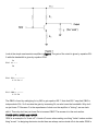
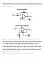
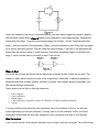
Look at the simple one-transistor amplifier in Figure 1. The gain of the circuit is given by equation EQ5 while the bandwidth is given by equation EQ-6.
Rc
EQ-5: Av = --Re
1
EQ-6: BW = --------------2 * PI * Rc * C
1
EQ-7: GBW = ----------2 * PI * Re
The GBW is found by multiplying Av by BW to get equation EQ-7. Note that EQ-7 says that GBW is
independent of Rc. So if we raise the gain by increasing Rc, we also lower the bandwidth. Why don't
we just lower C? Because C is the capacitance of what ever the amplifier is "driving", we are stuck
with it. Then why don't we just lower Re to increase GBW? The answer is in the next section.
TRADE-OFFS: SPEED and POWER
GBW is an example of a "trade-off". A trade-off occurs when making one thing "better" makes another
thing "worse". In designing electronic circuits there are always various trade-offs to be made. GBW is
a trade-off between gain and bandwidth. Speed and power-dissipation is another trade-off. When
designing an amplifier, it may be possible to increase the GBW (the "speed") if you are willing to have
it "run hotter" by dissipating more power.
Let's look again at the circuit in Figure 1. Suppose we lower Re to increase the GBW, but we want to
keep the same gain. Then we must also lower Rc. In amplifiers such as figure 1, the average (DC)
voltage across Rc is approximately half the supply voltage. So the power (P) dissipated in Rc is
V*V
EQ-8:
(Vcc / 2) * (Vcc / 2)
Vcc * Vcc
P = ------ = --------------------- = ---------R
Rc
4 * Rc
Note that the smaller Rc is, the more power is dissipated in it. So if Re and Rc are both lowered
proportionately, we will get an increased GBW but at the cost of more power being dissipated by the
circuit. The same analysis would apply to a digital circuit as well.
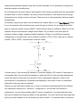
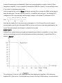
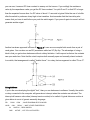
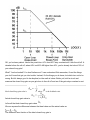
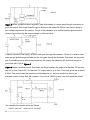
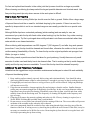
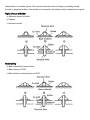
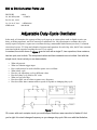
BODE PLOTS
A Bode Plot is a graph showing how gain and bandwidth are related in an amplifier. It is very useful,
and is very commonly found in books and magazine articles on electronics. A typical Bode Plot is
shown in Figure 2.
The vertical axis (Y-axis) is in dB. Remember that when dealing with amplifiers, dB is defined by
equation EQ-2 given above. The horizontal axis (X-axis) is the Log of the frequency, so each mark on
the horizontal axis represents a frequency 10 times higher than the previous mark. The distance from
one mark to another, from f to 10f, is called a "decade". The distance from f to 2f is called an "octave".
BREAK-POINT, ROLL-OFF, AND FEEDBACK
Figure 2 shows the maximum voltage gain (Av) of an amplifier as a function of frequency. There are
two important things to see on the graph. First is the "break-point" which occurs at the "breakfrequency" fB. Av is constant until the break-point. The second thing is that after fB, Av starts to "roll
off" at a constant rate of 20 dB per decade. The point where the graph crosses through the horizontal
axis is the GBW. A roll-off of 20dB / dec is typical of many amplifiers.
Figure 2 shows that the amplifier starts out with a gain of 100 dB, which is a gain of 100,000. That's
more gain than you need for most applications. So high-gain amplifiers in general, and op-amps in
particular, use "negative feedback" to reduce the gain to a usable level. A total discussion of negative
feedback is beyond the scope of this article. We will just say that negative feedback takes some of
the output signal and connects it back to the input in such a way that the signal fed back subtracts
from the input. The effect is to cause the amplifier to operate at a lower value of gain while the GBW
stays the same. With no feedback, the amplifier is said to be "open-loop". With negative feedback, it
is said to be "closed-loop".
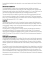
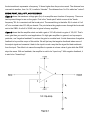
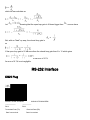
Figure 3 shows a 741 op-amp (an oldie but a goodie) in a closed-loop circuit. The gain is given by the
equation:
EQ-9:
Av = 1 + R1 / R2
Figure 4 shows how the Bode plot for the 741 has been changed by configuring it for a closed-loop
gain of 10. Note that the usable bandwidth is much greater than the original fB.
WRAP-UP
Connectors
INTRODUCTION
In electronics, connectors are one of those things we tend to take for granted. They're just something
hanging off the end of a cable so we can plug and unplug power or signals on some circuit. So what's
there to think about connectors? The answer is "plenty"!
Besides the obvious, such as having the right number of pins, there are several things to consider
when choosing a connector:
Cost: Nobody wants to spend more than they have to. But using the cheapest connector you can find
may not, in the end, be cost effective if it fails to do its job.
Ruggedness: Is it going to be plugged and unplugged once a year, or ten times a day?
Environment: Will it be exposed to the weather, such as on an outdoors antenna? How about salt water,
such as on a boat? Will it be subject to vibration, such as on a machine? Is someone likely to step on it?
Signals Type: Is it for power and ground? For analog or digital signals? If analog, what frequency? Is it
audio or RF? If digital, what clock speed or bit rate?
Power Level: If it's for power, is it for 24 Volts? Or 240 Volts? Or 2,400 Volts? Will it carry 0.25
Amps? Or 2.5 Amps? Or 25 Amps? Higher currents require larger, thicker pins. Higher voltages require
more insulation.
Signal Level: Is it for 2 Volt signals or 2 microVolt signals? Will the current be 5 milliAmps or 5
microAmps? Connectors used for very low signal levels (so-called "dry circuits") often have gold plated
pins.
Second Sources: Is it a standard type of connector available from many manufacturers, or is it available
only from one company?
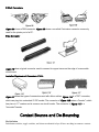
TYPES OF CONNECTORS
If you've been around electronic equipment for any length of time, then you know there are many
types of connectors. Here, in no particular order, are some of the common ones:
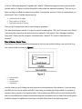
Power Connectors
Figure 1 shows a common type of 115 VAC receptacle used to connect the power cord to things such
as personal computers and test equipment.
Figure 2 shows a "Jones" or "Cinch-Jones" connector. These have been around for decades, and are
used in applications such as supplying power to a DC motor.
Audio Connectors
Like the Jones connectors, most of these have been around for decades. Figure 3 shows what is
commonly called an "RCA" plug and jack. They are two-conductor connectors typically used with
shielded cable. They are used in applications such as connecting microphones and small speakers to
audio amplifiers.
Figure 4 shows a "phone" (old telephone type) or "phono" plug and jack. They can be two or three
conductor connectors used for one (mono) or two (stereo) audio signals carried on a shielded cable.
There are several other types of connectors used for audio signals.
Modular (Telephone) Connectors These are used with UTP (unshielded twisted pair) cables. Figure 5
shows an RJ11 connector commonly used with 4-wire telephone cables. An RJ12 connector is the
same size but used with 6-wire cable. Figure 6 shows an RJ45 connector used with 8-wire local area
network (LAN) cables.
BNC and UHF Connectors
Figure 7 shows a BNC cable commonly used with shielded cable, such as RG58, carrying RF signals.
Exactly what BNC stands for is unclear, but most people think the B is for bayonet because of the
way the connector locks on to the receptacle. BNC connectors are common on electronics test
equipment such as oscilloscopes.
Figure 8 shows a UHF connector (UHF stands for Ultra High Frequency). Like the BNC connector, it
is used on coaxial cables carrying RF signals. It can be used on thicker cable such as RG8. A UHF
connector is threaded to screw onto the receptacle.
D-Shell Connectors
Figure 9A shows a DB9 connector. Figure 9B shows a so-called Centronics connector commonly
used for the printer port of a PC.
Edge Connector
Figure 10 show a typical connector used to connect to copper traces on the edge of a removable
circuit board.
Insulation Displacement Connectors (IDCs)
Figure 11 shows the types of connectors used with ribbon cables. Figure 11A is a "DIP" connector,
which can plug into a standard IC DIP socket. The connector of Figure 11B mates a "header", which
has pins on 0.1" centers and is common on circuit boards. The connector of Figure 11C is a
"shrouded" header.
Contact Bounce and De-Bouncing
The Definition
Push-button switches, toggle switches, and electro-mechanical relays all have one thing in common: contacts.
It's the metal contacts that make and break the circuit and carry the current in switches and relays. Because they
are metal, contacts have mass. And since at least one of the contacts is on a movable strip of metal, it has
springiness. Since contacts are designed to open and close quickly, there is little resistance (damping) to their
movement.
Because the moving contacts have mass and springiness with low damping they will be "bouncy" as
they make and break. That is, when a normally open (N.O.) pair of contacts is closed, the contacts
will come together and bounce off each other several times before finally coming to rest in a closed
position. The effect is called "contact bounce" or, in a switch, "switch bounce" See Figure 1. Note that
contacts can bounce on opening as well as on closing.
The Problem
If all you want your switch or relay to do is turn on a lamp or start a fan motor, then contact bounce is
not a problem. But if you are using a switch or relay as input to a digital counter, a personal computer,
or a micro-processor based piece of equipment, then you must consider contact bounce. The reason
for concern is that the time it takes for contacts to stop bouncing is measured in milliseconds. Digital
circuits can respond in microseconds.
As an example, suppose you want to count widgets as they go by on a conveyor belt. You could set
up a sensitive switch and a digital counter so that as the widgets go by they activate the switch and
increment the counter. But what you might see is that the first widget produces a count of 47, the
second widget causes a count of 113, and so forth. What's going on? The answer is you're not
counting widgets, you're counting how many times the contacts bounced each time the switch is
activated!
The Solution
There are several ways to solve the problem of contact bounce (that is, to "de-bounce" the input
signal). Often the easiest way is to simply get a piece of equipment that is designed to accept
"bouncy" input. In the widget example above, you can buy special digital counters that are designed
to accept switch input signals. They do the de-bouncing internally. If that is not an option, then you
will have to do the debouncing yourself using either hardware or software.
Using Hardware
A simple hardware debounce circuit for a momentary N.O. push-button switch is show in Figure 2. As
you can see, it uses an RC time constant to swamp out the bounce. If you multiply the resistance
value by the capacitance value you get the RC time constant. You pick R and C so that RC is longer
than the expected bounce time. An RC value of about 0.1 seconds is typical. Note the use of a buffer
after the switch to produce a sharp high-to-low transition. And remember that the time delay also
means that you have to wait before you push the switch again. If you press it again too soon it will not
generate another signal
Another hardware approach is shown in Figure 3. It uses a cross-coupled latch made from a pair of
nand gates. You can also use an SR (sometimes called an SC) flip flop. The advantage of using a
latch is that you get a clean debounce without a delay limitation. it will respond as fast as the contacts
can open and close. Note that the circuit requires both normally open and normally closed contacts.
In a switch, that arrangement is called "double throw". In a relay, that arrangement is called "Form C".
Using Software
If you're the one developing the digital "box", then you can debounce in software. Usually, the switch
or relay connected to the computer will generate an interrupt when the contacts are activated. The
interrupt will cause a subroutine (interrupt service routine) to be called. A typical debounce routine is
given below in a sort of generic assembly language.
DR:
PUSH
LOOP:
PSW
CALL
IN
CMP
; SAVE PROGRAM STATUS WORD
DELAY ; WAIT A FIXED TIME PERIOD
SWITCH ; READ SWITCH
ACTIVE ; IS IT STILL ACTIVATED?
JT
LOOP
; IF TRUE, JUMP BACK
CALL
DELAY ;
POP
PSW
EI
RETI
; RESTORE PROGRAM STATUS
; RE-ENABLE INTERRUPTS
; RETURN BACK TO MAIN PROGRAM
The idea is that as soon as the switch is activated the Debounce Routine (DR) is called. The DR calls
another subroutine called DELAY which just kills time long enough to allow the contacts to stop
bouncing. At that point the DR checks to see if the contacts are still activated (maybe the user kept a
finger on the switch). If so, the DR waits for the contacts to clear. If the contacts are clear, DR calls
DELAY one more time to allow for bounce on contact-release before finishing.
A debounce routine must be tuned to your application; the one above may not work for everything.
Also, the programmer should be aware that switches and relays can lose some of their springiness as
they age. That can cause the time it takes for contacts to stop bouncing to increase with time. So the
debounce code that worked fine when the keyboard was new might not work a year or two later.
Consult the switch manufacturer for data on worst-case bounce times.
Making Electrical Measurements Part 1
The Fundamentals
In electronics, the fundamental physical property is charge. Charged particles, such as electrons and protons,
interact with each other over time and distance by exchanging discrete bundles of energy called photons. It is
the ebb and flow of photons that gives rise to electro-magnetic phenomenon such as light and radio waves. It is
our ability to control and use electro-magnetism that lets us build all our wonderful gadgets.
Physicists have worked out elegant mathematical structures to describe electro-magnetic fields in
time and space. For the most part, we do not deal directly with such fields in the equipment and
circuits we work on every day. Instead, we deal with them one step removed by working with voltages
and currents. Roughly speaking, you can think of voltage as corresponding to the electric field and
current as corresponding to the magnetic field.
Making Measurements
To measure a quantity such as voltage or current, we must make that quantity interact with an
instrument in such a way that the instrument changes in a way that we can sense.
For example, Figure 1 shows an old-fashioned meter-movement for measuring current. The current
flows through the coil of the meter and creates a magnetic field proportional to the current.
The magnetic field attracts an iron pointer which is held back by a spring. The more current, the more
magnetic "pull", and the more the pointer moves.
Modern digital meters work on a completely different principle, but they still involve using the voltage
or current you are measuring to do something to the meter which causes a change.
The Limitation of Measurements
The fact that the quantity being measured must interact with the instrument making the measurement
implies that we change the value of the thing we are measuring by the very act of measuring it. In
other words, there is always a limitation on how accurately we can measure voltage or current. There
will always be some error, or uncertainty, in the numbers we get from our instruments and meters.
For most of the measurements we make every day, a small error is not important. For example, if the
5-volt power supply is actually 5.001 volts, it will not make a difference to our computer. However, it is
good to keep in mind that there are limits to accuracy. Think of it as "noise".
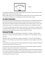
Accuracy as a Percentage
The accuracy of an instrument is often stated as a percentage. For example, a voltmeter may be
specified as 1% accurate. An important question is: 1% of what? Is it 1% of the reading or 1% of the
"full-scale"?
Suppose you have a meter which reads voltages in the range of 0 to 100 volts. Then the full-scale
value is 100 volts. Now suppose you use that meter to measure an unknown voltage, Vx, and it reads
50 volts.
If the accuracy of your meter is ±2% of the reading, then the actual voltage is somewhere between 49
volts and 51 volts since 2% of 50 volts is 1 volt.
On the other hand, if the accuracy is ±2% of full-scale (or f.s.) then the actual voltage is somewhere
between 48 volts and 52 volts since 2% of 100 volts is 2 volts.
Accuracy is often given as percentage of full-scale, which means you should use the lowest scale you
can to make the measurement. Suppose a 5% voltmeter has two ranges, 0-10 volts and 0 to 20 volts.
If you want to measure a 9-volt battery then you should use the 10-volt scale since 5% of 10 volts is
0.5 volts while 5% of 20 volts is 1.0 volts.
Digital Meters: That Last Digit
Digital meters are often compared by the number of digits they can display. For example, a 2-digit
meter can display values from 00 to 99 while a 3-digit meter can display values from 000 to 999.
Suppose you have a 2-digit voltmeter that reads 0 to 99 volts. Effectively it has a full-scale capability
of 100 volts. Suppose you use it to measure a voltage with a value of 50.5 volts. What will the meter
read? The only choices are 50 or 51, so either way there will be an error. That fact about digital
meters is expressed by saying that all readings are plus or minus a count of one.
Digital Meters: Accuracy vs. Resolution
The fact that the reading on a digital meter is always uncertain by a count of 1, either up or down,
defines the resolution of the meter. Resolution is the smallest change an instrument can measure (or
"resolve"), so in a digital instrument it is the last bit: +/- a count of 1.
Like accuracy, resolution can be expressed as a percentage. A 2-digit meter has 1% resolution (1
count out of 99) while a 3-digit meter has 0.1% resolution (1 count out of 999). However, resolution is
not accuracy. A 3-digit meter has 0.1% resolution buy may only have 0.5% f.s. accuracy. Read the
specifications of the meter carefully: it is usually the case that the resolution is better than the
accuracy.
Extra Resolution
In a digital meter, it is relatively easy to increase resolution by adding another digit. It is more difficult
to make that extra digit accurate. Even if the last digit on a meter is not accurate, there are times
when that extra resolution is useful.
For example, in radio circuits, you sometimes have to "tune-for-a-dip", meaning you adjust the
frequency until you hit resonance as indicated by the amplifier current going to minimum (not zero)
value. The exact value is not as important as the fact that it is minimum. Look at the table below
which shows actual values compared to measured values.
Actual
Freq.
Measured
Current (mA)
Current (mA)
--------------------------------------------f1
16.99
16.88
f2
16.96
16.85
f3
16.93
16.82
f4
16.91
16.80
f5
16.94
16.83
f6
16.97
16.86
A 3-digit meter, even if it was accurate, would not let you see the minimum at f4 since it would read
16.8 for f3, f4 and f5.
For the extra resolution to be useful, as in the above example, it is necessary that it "do the right
thing". That is, as the actual value increases, the measured value increases and as the actual value
decreases, the measured value decreases. Such "doing the right thing" is referred to as being
monotonic. If you do not have monotonicity, the extra resolution is useless.
Making Electrical Measurements Part 2: Loading
Meter Loading
When making a measurement with a volt-meter, an oscilloscope, or any type of electronic measurement
equipment, it is important to understand the concept of loading if you want to be sure your readings are
accurate.
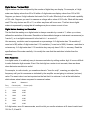
For example, suppose I use a volt-meter to measure the DC voltage at the output of a voltage-divider
as shown in Figure 1, and I get a reading of 4 Volts. Assuming my meter is working properly, am I
sure it's a good reading? Well, that depends on two things: the values of the resistors in the circuit,
and the input impedance of the meter. In order to see what's going on, I need to look at the
Thevenin's Equivalent Circuit for the voltage
divider
If you're not familiar with a Thevenin's Equivalent, it can be found in any book on circuit analysis.
Basically, it's a single voltage (Vth) in series with a single resistor (Rth) as shown in Figure 2. The
voltage (Thevenin's Voltage) is what you would measure with a perfect volt-meter. The resistance
(Thevenin's Resistance) is found from R = E/I where E is the Thevenin's Voltage and I is the current
you would get if you were to short-circuit the output to ground
For the voltage divider I'm trying to measure, since both resistors are equal, Vth would be V/2 and Rth
would be R/2. Figure 3 shows my meter as a resistor connected to the Thevenin's Equivalent of the
voltage divider. Note that the input impedance of the meter looks like a resistor forming another
divider. So the voltage across the leads of my meter is not Vth as you might expect, but is a value I
can calculate as:
Rin
Vm = ----------- x Vth
Rin + Rth
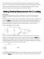
Now suppose that V is 12 Volts and R is 2k Ohms. Then Vth will be 6 Volts and Rth will be 1k Ohm.
Suppose that Rin of the meter is 10 Meg-Ohms. Using the above equation I get:
10,000k
Vm = -------------- x 6 Volts = 5.9994 Volts
10,000k + 1k
Which, on a typical 3-digit meter, will read 6.00 volts. No problem since that's the right reading.
But what if R in the divider is 2 Meg-Ohms. Then Rth is 1 Meg-Ohm and the equation will give:
10,000k
Vm = -------------- x 6 Volts = 5.4545 Volts
11,000k
Which, on a typical 3-digit meter, will read 5.45 Volts. Now I have a problem. The reading is wrong
because the meter loaded-down the circuit I was trying to measure. If R was 20 Meg-Ohms it would
be even worse!
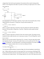
What can I do to solve the problem? A few things. First, I can see if I can get a meter with a higher
input impedance. Second, I can use a X10 probe if there is one for my meter (see Tech Tip on X10
probes). If all else fails, I can use a little math. If I know the input impedance of my meter and the Rth
of the circuit I'm trying to measure, then I can correct my readings as follows:
Rin + Rth
True Voltage = Measured Voltage x -----------Rin
If you are using a digital multimeter to measure voltage, then the input impedance is typically high
(say, 10 Meg), and the same value for all input ranges. But if you are using an old-fashioned VOM,
then the input impedance depends on the range the meter is set to. For instance, if the VOM is rated
at 10k Ohms per volt and is on the 0 - 50 Volt range, then Rin is 10k x 50 or 500k Ohms. But on the 0
- 5 Volt range Rin will only be 10k x 5 or 50k Ohms. Typical ratings for VOMs are 1 k Ohm per Volt at
the low end to 20k Ohms per Volt at the high end.
But what if I don't know the input impedance of my meter, or if there is no way to calculate Rth. Can I
find out if I have a loading problem? Yes, by running a little test. Measure the voltage with your meter.
Then put a 100 K resistor in series with the red lead of the meter and measure the voltage again. If
the readings change significantly, then you may have a problem.
So know the input impedances of all your measurement equipment. You'll find it on the specifications
page in your user's manual. And have some idea of the internal resistances in the circuits you are
measuring. Then you won't be fooled by loading. In later technical tips we will look at other factors
that affect the accuracy of your measurements.
Making Electrical Measurements Part 3:
Testing Diodes and Transistors
BACKGROUND
One of the nice things about solid-state devices is that, under normal conditions, they rarely go bad. However,
"rarely" is not the same as "never". And if conditions are not "normal", if an excessive voltage gets to a
semiconductor, it can be damaged. In this article we will discuss how to test for a damaged transistor or diode.
Device testing can be done at two levels: functional and parametric. A functional test determines
whether or not the device works well enough for the intended use. A parametric test measures all
device parameters to see if they meet the specified values. In the production of semiconductor
devices, it is often the case that functional testing is done on all units while parametric testing is done
on a small percentage of the units as test samples.
For the most part, the performance of semiconductor devices does not deteriorate gradually over a
period of time. Typically, transistors and diodes work well up to the point where they stop working
completely, so all we will need to do is make a few simple functional tests.
TESTING SILICON DIODES (NOT LED OR ZENER)
To test a silicon diode such as a 1N914 or a 1N4001 all you need is an ohm-meter. If you are using
an analog VOM type meter, set the meter to one of the lower ohms scales, say 0-2K, and measure
the resistance of the diode both ways. If you get zero both ways, the diode is shorted. If you get
INFINITY both ways, the diode is open. If you get INFINITY one way but some reading the other way
(the value is not important) then the diode is good.
If you use a digital multi-meter (DMM), then there should be a special setting on the Ohms range for
testing diodes. Often the setting is marked with a diode symbol
Measure the diode resistance both ways. One way the meter should indicate an open circuit. The
other way you should get a reading (often a reading around 600). That indicates the diode is good. If
you measure an open circuit both ways, the diode is open. If you measure low resistance both ways,
the diode is shorted.
TESTING DIODES IN CIRCUIT
The procedures described above assume the diode under test is not part of any circuit. If you are
trying to test a diode that is on a circuit board or otherwise connected to other components, then you
should disconnect one end of the diode. On a circuit board you can unsolder one end of the diode
and lift it off the board. Make sure that you first disconnect all power going to the circuit before you
disconnect the diode. After disconnecting one end, proceed as described above.
KNOW POLARITY OF YOUR METER
When set to measure resistance, both VOMs and DMMs apply voltage to the test leads. You should
know which lead is positive. Don't assume the red lead is positive, it may not be. Use another meter
set to measure DC volts on, say, the 20V scale and determine which lead of your Ohm-meter is
positive.
Another way is to take a diode you know is good and find which way you need to put the leads to get
an Ohms reading. At that point, the positive lead is on the anode and negative lead is on the cathode
(cathode is the banded end.)
One reason to know the polarity of your meter is so you can determine which end of a diode is the
cathode if the band has been removed. Also, as we will see below, you can use your Ohm-meter to
tell an NPN transistor from a PNP if you know which meter lead is positive.
TESTING ZENERS
If you just want to know if a Zener diode has opened-up or shorted-out, then just test it as described
above for standard diodes. if you want to measure its Zener voltage level, you will have to build a
circuit as shown in Figure 3.
The power supply voltage should be set to a value slightly higher than the Zener value. For example,
for a 12 volt diode, the supply voltage should be about 15 volts. The value of the resistor R should
limit the current to about a milliAmp. For example, using 15 volts with a 12 volt Zener, use a 3.3K
resistor. The exact value is not critical.
Once the circuit is built, just read the Zener voltage off the meter (if you read 0.6 volts, reverse the
diode). NOTE: Any diode will become a Zener diode if you apply enough voltage to it.
TESTING LEDS
LEDs have a larger voltage-drop across them than regular diodes. Depending on the LED, the drop
can be between 1.5 to 2.5 volts. If you have a DMM with a diode setting on the Ohms scale (see
above), then you may be able to test an LED as you test a standard diode. The difference will be that
the meter will read 1600 or 50 when the diode conducts instead of the 600 you read on a silicon
diode.
If you can't use your multi-meter, then build the circuit shown in Figure 4 and see if the LED light up.
If the LED doesn't light, reverse polarity on the diode. If it still doesn't light, it's bad. (See Figure 4).
TESTING ZENERS AND LEDS IN CIRCUIT
To test a Zener or an LED while it is in a circuit, you just need a volt-meter.
For a Zener, just measure the voltage across it. Using a VOM or a battery-operated DMM, put the
black lead on the anode and the red lead on the cathode. You should read the Zener voltage. If you
read zero volts, the Zener is shorted or the resistor feeding the Zener is open or not getting voltage. if
you read a value higher than the Zener voltage, the Zener is open.
For an LED that is supposed to be lit but isn't, use a VOM or battery-operated DMM to measure the
voltage across it. If you measure more than 3 volts or so, the LED is open.
TRANSISTORS
As with diodes, it is usually the case that a transistor either works or it doesn't. So again we will be
able to make a few simple tests with a meter to see if a transistor is good or bad.
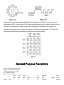
You can think of a transistor as two back-to-back diodes in one package as shown in Figure 5.
Note that transistors come in two basic types: NPN and PNP. The letters C, B, E stand for
COLLECTOR, BASE, EMITTER which are the names of the three leads which come out of a
transistor.
Transistors come in many different case styles, three of which are shown in Figure 6. It is important to
know where C, B, E are for any given case.
TESTING TRANSISTORS
Assuming you know if the transistor is NPN or PNP, and assuming you know where B, C, and E are,
then just test the B-C junction and the B-E junction as if they were standard diodes. if one of those
junctions is a "bad diode", then the transistor is bad.
Also, check the resistance from C to E using a higher Ohms scale (say, the 2 Meg scale). Be sure
your fingers don't touch the metal test points or you will just measure your skin resistance.
If the transistor is good, you should get an open-circuit reading from collector to emitter. NOTE: the
above assumes silicon. With germanium transistors you may measure a high resistance from C to E.
USING METER TO SEPARATE NPN FROM PNP
If you have a transistor but you don't know if it is NPN or PNP, then you can find out which it is using
your Ohm-meter if you know which lead of your meter is positive.
Assuming you know where C, B, and E are on the transistor, do the following. Connect the positive
lead of your Ohm-meter to the base. Touch the other lead of your meter to the collector. If you get a
reading, the transistor is NPN. To verify, move the lead from the collector to the emitter and you
should still get a reading.
If your meter reads open-circuit, then connect the negative lead to the base and touch the positive
lead to the collector. If you get a reading, then the transistor is PNP. Verify by measuring from base to
emitter.
THINGS TO WATCH FOR
Some transistors have diodes from collector to emitter built into them. They will not read open-circuit
when measuring resistance between C and E.
Some transistors have resistors from base to emitter built into them. They will read that resistance
when measuring Ohms B to E.
Some transistors are Darlingtons. They have a higher reading base to emitter which may appear as
an open on a VOM.
CHECKING TRANSISTORS IN CIRCUIT
With power disconnected from the circuit, you can try some of the above measurements on
transistors that are in the circuit. However, your readings can be deceptive due to resistors and other
components in the circuit. You can try disconnecting the base lead from the circuit before making
measurements. Be sure to reconnect it after testing.
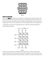
Keypads
HOW THEY ARE BUILT
A keypad, with 12 or 16 keys, is one of the most commonly used input devices in microprocessor
applications. The telephone keypad shown below in Figure 1 is a typical example. Like most such
keypads, it is wired as an X-Y switch matrix as shown in Figure 2. The normally-open switches
connect a row to a column when pressed. Note that the resistors are not part of the keypad. Because
this keypad has 12 keys, it is wired as 3 columns by 4 rows. A 16 key pad would have 4 columns by 4
rows.
Figure 1
HOW THEY ARE READ
As shown in Figure 2, the columns are connected to +5 Volts (logic level 1) by pull-up resistors. The
other ends of the columns are connected to an input port so that the logic level on each column can
be read. The rows are connected to an output port where the software pulls one row at a time low in a
repeating cycle. First row 0 is low while rows 1,2, and 3 are kept high. Then row 0 is pulled high, row
1 is pulled low, and rows 2 and 3 are kept high. And so on until each row has been pulled low, at
which point the cycle repeats.
Figure 2
Each time a row is pulled low, the software will read in the columns. If no key is pressed, all the
columns will be high. If a key is pressed, one column will be connected to one row. When that row is
pulled low, that column will also go low. By knowing the row number and column number that are low,
the software knows which key was pressed. The software runs through the scan cycle in a matter of
microseconds, so no matter how fast you press the keys the software will catch it.
Table 1 shows the pin assignments for the Electronix Express keypad (part number 1704627).
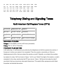
WIRING DIAGRAM FOR TELEPHONE-TYPE
3-BY-4 X - Y MATRIX KEYPAD
COL 0
COL 1
COL 2
PIN 4
PIN 2
PIN 6
ROW 0
PIN 3
1
2
3
ROW 1
PIN 8
4
5
6
ROW 2
PIN 7
7
8
9
ROW 3
PIN 5
*
0
#
Table 1
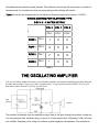
THE OSCILLATING AMPLIFIER
You say you built a simple little battery-powered audio amplifier, and instead of amplifying the darn thing just
sits there and oscillates? You say you put a capacitor from +V to ground and it still oscillates? You say you
don't know what to do next? Cheer up, you can fix it!
The problem is feedback from the amplifier's output back to it's input through the positive voltage rail.
You say you knew that, and that's why you put a 10 uF cap across the 9 Volt battery? Well, let's look
at it carefully. Suppose you're using one of those popular capacitor microphones. They need to be
biased to +V to operate. Look at the circuit in Figure 1. You see that the DC bias voltage on the
microphone comes directly from +V via a resistor. So if there is any AC "ripple" on +V, it will show up
at the input to the amplifier. Where would ripple come from you ask? Well I'll tell you.
Real batteries have some internal resistance, and as you use them that resistance gets bigger. Also,
the wires used to build the circuit (or the copper traces on a circuit board) have a small amount of
resistance. Amplifiers such as the LM386 can easily put out 500 mW of signal, which from a 9-volt
battery means an AC current of over 50 mA due to the audio signal.
Look at Figure 2. Suppose the internal resistance of the battery is 1 Ohm. Then 50 mA of AC current
will cause 50 mV of AC ripple on the +9 rail. Likewise, suppose you have .05 Ohms of resistance in
the wiring. Then you'll get 2.5 mV of ripple. While 2.5 mV may not sound like much, note that through
the biasing it ends up at the input to the amplifier, where it causes more output on the load leading to
more current being drawn and more ripple voltage getting back to the amplifier input. In other words,
you've got feedback!
What about the cap across the battery you ask? At 60 Hertz, the impedance of a 100 uF cap is about
27 Ohms, which is considerably bigger than the resistances we've been talking about. A capacitor
alone may not be enough. What you need is decoupling. Figure 3 shows a typical decoupling circuit.
First off, you want to connect the battery (or other voltage source) directly to the amplifier with a
capacitor right across the amplifier's power pins. Then you want to build an RC low-pass filter into the
+V rail for the rest of the circuitry (RD and CD). You want to make the break-frequency ( 1 / 2piRC ) at
least 10 times lower than the feedback frequency that is occurring. Be careful that you don't make RD
too big, or the DC drop across it will be too much.
For example, if the problem is 60 Hz, then with RD = 1000 Ohms C should be at least 27 uF, with
values like 47 uF or 100 uF being better. Use the formula:
1
C = ---------------
where f is the troublesome frequency.
2p x (10f) x R
Another approach is to use a zener diode. Zener diodes of 5.1 V or higher are actually avalanche
diodes, which have a very low resistance when they are conducting at their break-down voltage. Look
at Figure 4. Basically, we power the amplifier from the battery, but power the rest of the circuit from a
separate power rail. See Figure 4.
In summary, accidental feedback through the power supply is one of those things designers must be
aware of, otherwise it sneaks up and bites you.
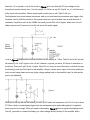
Notes On Gain-Error In Op-Amp Amplifiers
This article is about the errors you can make in calculating the gain of an op-amp amplifier circuit. I'm assuming
here that you are familiar with op-amp amplifier circuits. But let's do a quick review anyway.
As you know, the key idea in op-amp circuits is that you start with a very high gain, and then trade off
that gain in exchange for increased bandwidth and improved characteristics. What characteristics?
You remember; things like input impedance (it gets bigger), output impedance (it gets smaller),
distortion (it becomes less), and so forth.
. Open-loop gain is the gain of the op-amp chip itself
Op-amps have enormous open-loop gain
with no feedback. That gain is too big to be used, so you lower it with negative feedback. The gain
with feedback is the closed-loop gain
.
Below are schematics for the two basic feedback circuits: the inverting amplifier and the non-inverting
amplifier. The gain equation for each circuit is included. Notice that the gain equations do not include
frequency as a variable.
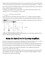
Before we get to the punch-line of this article, there's a short story to tell. So, please be patient.
Many books either say or imply that the closed-loop gain doesn't change with frequency until the line
for ACL meets the line for AOL on the amplifier's Bode plot. What's a Bode plot? C'mon, you
remember! It's a graph that shows how the gain of an amplifier "rolls off" as signal frequency
increases. Many op-amps, like the lovable old 741, roll off at 20 dB per decade. (A decade is when
the frequency changes by a factor of 10, but you knew that.) The open-loop gain of an op-amp starts
rolling off at a relatively low frequency, maybe 10 Hertz. But they have so much AOL that it doesn't
get to 1 (0 dB) until you get up to mega-Hertz.
Hey! Someone left a Bode plot right here for us to look at! It could be for a 741.
OK, you've been patient. Here's the punch-line: ACL does NOT stay constant until it hits the roll-off. A
decade before the roll-off, when AOL is still 20 dB higher than ACL, you've already lost about 10% of
your closed-loop gain!
What? You're shocked? You don't believe me? I can understand. But remember, it's not the things
you don't know that get you into trouble. Instead, it's the things you do know, but which turn out to be
wrong. But it's always good to be skeptical, so the math is below. Better yet, build a circuit and
measure the closed loop gain as you get close to the roll-off and see if the gain stays constant or not.
Ideal closed-loop gain value is
where
is the feedback ratio
Actual closed-loop gain value is
Let's call the ideal closed loop gain value
We can express the difference between the ideal value and the actual value as
The difference as a fraction of the ideal closed-loop gain is
which we can calculate as
Let
meaning that the open-loop gain is N times bigger than
now we have
But, with an "ideal" op-amp, the closed-loop gain is
so
If the open-loop gain is 20 dB more than the closed-loop gain then N = 10 which gives
or an error of 9.1%
An error of 9.1% is not negligible.
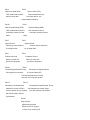
RS-232 Interface
DB25 Plug
SIGNALS FROM TERMINAL
SIGNALS FROM MODEM
---------------------
------------------
PIN 2
PIN 3
Transmitted Data (TD)
Data from terminal.
Received Data (RD)
Data from modem
PIN 4
PIN 5
Request to Send (RTS)
Clear to Send (CTS)
Tells modem that terminal
Tells terminal that it may
wants to send data.
now place data on the
transmit data line (PIN 2).
PIN 20
PIN 6
Data Terminal Ready (DTR)
Data Set Ready (DSR)
Tells modem that terminal is
Tells terminal modem is
connected, powered up and.
ready
PIN 7
connected, powered up and
ready.
PIN 7
Signal Ground
Signal Ground
Common ground reference
for all signal lines.
PIN 1
Common ground reference
for all signal lines.
PIN 1
Protective Ground
Protective Ground
Safety or power line
Safety or power line
ground for equipment.
PIN 24
ground for equipment.
PIN 8
Transmit Signal Element Timing
Clock signal from terminal.
Received Line Signal Detector
or Carrier Detect (CD)
Tells terminal that carrier is being
received from computer modem.
PIN 14
PIN 15
Secondary Transmitted Data
Identical in function to PIN 2
except it applies only to systems
Transmission Signal Element Timing
Clock signal from modem (used
only with synchronous modems.
with full secondary channel
implemented.
PIN 22
Ring Indicator
Signal telling terminal
that phone line is "ringing".
i.e. there is an incoming call.
PIN 19
PIN 17
Secondary Request to Send
Received Signal Element Timing
Tells modem to turn on the
Clock signal from modem (used
secondary channel carrier used
only with synchronous modems).
for HD supervisor operation.
PIN 23
PIN 16
Data Rate Signal Selector
Secondary Received Data
Used by Modem/Terminals with
Identical in function to PINs 3 and 5
programmable data rate selection.
except as they apply only to systems
with full secondary channels implemented.
PIN 13
Secondary Clear to Send
Identical in function to Pins 3 and 5
except as they apply only to systems
with full secondary channels implemented.
PIN 12
Secondary Received Line Dignal Detect
Tells terminal that carrier is
present on secondary channel.
used for HD supervisor operation.
PIN 21
Signal Quality Detector
Used by some modems which incorporate
signal evaluating circuitry to advise
terminal that present signal is poor
and a high error rate is probable.
Pins receiving signal
from modem:
Pins receiving signals
from terminal
3, 5, 6, 8, 12, 13,
2, 4, 14, 19, 30, 23, 24.
15, 16, 17, 21.
DB9
DB9
DB25
PIN
PIN
NAME
DESCRIPTION
------------------------------------------------1
8
CD
RLSD Carrier Detect
2
3
RD
Receive Data
3
2
TD, SD
4
20
DTR
Data Terminal Ready
5
7
GND
Signal Ground
6
6
DSR
Data Set Ready
7
4
RTS
Request to Send
8
5
CTS
Clear to Send
9
22
RI
Transmit Data
Ring Indicator
Keep in mind that on many computers, COM1 and COM2 are wired differently, COM1 being DTE,
COM2 being DCE. If COM2 is configured as a DCE, a null modem cable with TX and RX reversed
will be needed to use it. Some 9 pin to 25 pin adapters, but not all of them, also reverse TX and RX.
Importance of X10 Probes
Here is something you may have experienced: You build a simple digital circuit using flip-flops, like a
ripple-counter, and it seems to be working OK. But as soon as you try to look at one of the Q outputs
with your scope, things get funny. You don't see what you expect to see; maybe the counter even
stops working. What's going on?
The answer may be your scope probe. Instead of using an actual scope probe, you may have a
length of coaxial cable ("co-ax") with a BNC connector at one end and a couple of alligator clips at the
other. It may work fine for looking at lower frequency sine-waves, but it's the wrong thing for digital
circuits.
Here's the problem: that piece of coax has a certain amount of capacitance (50 pF/foot is typical) and
a certain amount of inductance. But it has very little resistance. So what you have is a resonant circuit
with very little damping. Trying to put a fast rise-time digital signal through it is like hitting a bell with a
hammer. That cable is going to "ring".
When a cable rings, a signal applied at the input end will travel up the cable, echo off the other end,
and travel back down to the input where it arrives, out of phase, on top of the signal you're trying to
measure. The result is that at the point you attach the cable, you cause transients: very narrow
voltage "spikes" that go both positive and negative.
Getting back to your digital circuit, by causing a voltage spike in the middle of your counter you cause
the flip-flops to change state. Obviously a spike on an input can "flip" your flip-flop. But so can a spike
on an output. The solution is to use a real scope probe instead of a piece of co-ax. Usually you want
a properly adjusted "X10" probe. Probes can be X1 ("times-one") or X10 ("times-ten"). Often a probe
has a switch on it so you can use it in either X1 mode or in X10 mode.
A scope probe is built to minimize ringing by adding resistance. A X1 is better than a piece of co-ax,
but a X10 probe is more effective than a X1. A X10 probe has the effect of reducing capacitance by a
factor of ten. The trade-off is that is also attenuates the signal by a factor of ten. That is, 1/10 the
signal applied to the tip of the probe actually reaches the input of the oscilloscope.
Above is the schematic of the circuit inside a X10 probe. You can see that it is basically a voltage
divider. Rp and Cp are selected to form a 10 to 1 divider with the input of the scope. Assume that the
scope has 1 Meg-Ohm input resistance and 100 pF of input capacitance. Then Rp is 9 Meg-Ohms
and Cp is 9 pF (remember: small C gives big X). Note that Cp is adjustable. That's to allow for
adjusting the response of the cable to fast rise times. Often Cp can be adjusted with a small
screwdriver. It may be located at the probe end of the cable, or at the end that attaches to the scope.
Most scopes have a "calibrator output" somewhere on the front panel. It supplies a square-wave to
look at with your probe. Adjust Cp until the rising edge of the square-wave looks like Figure 2 below.
Now you should be able to look at signals in your digital circuits without flipping your flops. Also, if you
are using a frequency counter to measure the frequency of a digital signal, then ringing in the coax
will give you a false reading. Again, the solution is a X10 probe.
SHUNT REGULATOR
The lab manuals for many DC circuits courses, including the ones that come with popular text books,
have experiments with circuits like the one shown in figure 1.
The problem with them is that sometimes the measured values of voltage and current don't agree
with the calculated values. It seems like a mystery: does circuit analysis not always work? Of course it
does!
The problem is likely to be in the power supply you're using. Circuits like the one in Figure 1 assume
that you are using batteries to supply the voltage. An ideal battery will sink current as well as source
current. That means that current can flow "backwards" into the battery.
Look at Figure 2 (we are using conventional current here). Using Ohm's Law, we can calculate the
current as:
E
I = ---- =
R
V1 - V2
12 - 6
---------- = -------- = 6 mA.
R
1000
But if you are using a typical power supply instead of batteries, you will measure 0 mA. What's more,
you will measure 0 Volts across the resistor. What's going on?
The answer is that the typical power supply uses a series regulator. A simplified schematic of a series
regulator is shown in Figure 3.
If you apply a voltage to the emitter that is greater than what the supply is set to put out, then you
reverse bias the transistor. That means that current can flow out the emitter of the transistor, but
current can not flow into the emitter. In fact, if too much reverse bias is applied to the transistor it will
be damaged. So often a diode is put in series with the output as protection.
Is there some way to get a power supply to sink current? Yes there is! You can use a circuit called a
shunt regulator.
Figure 4 shows a simplified shunt regulator. Note that instead of current going through a transistor to
get to the output, the current flows through a resistor to the output. By Ohm's Law, there is going to
be a voltage drop across the resistor. The job of the transistor is to conduct just the right amount of
current to ground so that the output voltage is at the set value.
If there is no load on the supply, all the current goes through the transistor. If there is a resistive load,
some current goes through the load and the rest goes through the transistor. But here's the important
part: if something tries to drive current back into the supply, the transistor will shunt that current to
ground as well. Look at Figure 5.
Figure 6 shows a practical circuit. The diodes are there because the output of a standard 741 op-amp
can not go from "rail-to-rail". So when the 741 output tries to go to zero, it can only go as low as about
2 Volts. That would mean the transistor would always be on, and you wouldn't be able to get
maximum output voltage from the regulator. If you use a CMOS op-amp, you won't need the diodes.
You calculate the resistor values as follows:
SUPPLY VOLTAGE - MAX OUTPUT VOLTAGE
R1 = --------------------------------------
MAXIMUM OUTPUT CURRENT
2
WATTAGE of R1 = (SUPPLY VOLTAGE) / R1
MAXIMUM SINK CURRENT
BASE CURRENT = -------------------------MINIMUM BETA of TRANSISTOR
SUPPLY VOLTAGE - DIODE DROP
R2 = ----------------------------BASE CURRENT
2
WATTAGE of R2 = (MAX CURRENT) x R2
EXAMPLE:
SUPPLY VOLTAGE = 20 V
MAX OUTPUT VOLTAGE = 10 V
MAX OUTPUT CURRENT = 100 mA
MIN BETA = 50
DIODE DROP (3 + 1 for BASE-EMITTER JUNCTION) = 4 x 0.625 V = 2.5 Volts
20 V - 10 V
10 V
R1 = -------------- = ----- = 100 Ohms
100 mA
0.1 A
WATTS = (20) x (20) / 100 = 4 W (use a 5 Watt resistor)
200 mA
BASE CURRENT = ------ = 4 mA
50
18 V
R2 = ----- = 4.5 K Ohms (Use 4.7 K Ohms)
4 mA
WATTS = (.004) x (.004) x (4700) = 75 mW (use 1/4 Watt)
You can use a value as low as 1 K for R2 to provide some over-drive capability since a 741 can
supply up to 20 mA. If you use a CMOS op-amp, check it's maximum current output.
To develop a voltage for the adjustable set-point, we used a 15 V, 1 W zener diode and a 4.7 K trimpot. To calculate the series resistor for the zener, we just used:
VOLTAGE DROP
(20 - 15) V
R = ------------ = ------------- = 250 Ohms. We used 200 Ohms.
ZENER CURRENT
20 mA
WATTS = (5V) x (5V) / 200 = 125 mW (Use 1/4 Watt)
Note that you don't have to build a whole new power supply to use this circuit. It can be connected to
the output of a standard supply.
Better Soldering
(A COOPERTools Reprint)
Purpose
We hope this short manual will help explain the basics of Soldering. The emphasis will be on the care and use
of equipment.
Overview
Soldering is accomplished by quickly heating the metal parts to be joined, and then applying a flux
and a solder to the mating surfaces. The finished solder joint metallurgically bonds the parts - forming
an excellent electrical connection between wires and a strong mechanical joint between the metal
parts. Heat is supplied with a soldering iron or other means. The flux is a chemical cleaner which
prepares the hot surfaces for the molten solder. The solder is a low melting point alloy of non ferrous
metals.
Solder and Flux
Solder is a metal or metallic alloy used, when melted, to join metallic surfaces together. The most
common alloy is some combination of tin and lead. Certain tin-lead alloys have a lower melting point
than the parent metals by themselves. The most common alloys used for electronics work are 60/40
and 63/37. The chart below shows the differences in melting points of some common solder alloys.
Tin/Lead
Melting Point
40/60
460 degrees F (230 degrees C)
50/50 418 degrees F
(214 degrees C)
60/40 374 degrees F
(190 degrees C)
63/37 364 degrees F
(183 degrees C)
95/5 434 degrees F
(224 degrees C)
Most soldering jobs can be done with fluxcored solder (solder wire with the flux in a "core") when the
surfaces to be joined are already clean or can be cleaned of rust, dirt and grease. Flux can also be
applied by other means. Flux only cleans oxides off the surfaces to be soldered. It does not remove
dirt, soot, oils, silicone, etc.
Base Material
The base material in a solder connection consists of the component lead and the plated circuit traces
on the printed circuit board. The mass, composition, and cleanliness of the base material all
determine the ability of the solder to flow and adhere properly (wet) and provide a reliable connection.
If the base material has surface contamination, this action prevents the solder from wetting along the
surface of the lead or board material. Component leads are usually protected by a surface finish. The
surface finishes can vary from plated tin to a solder - dipped coating. Plating does not provide the
same protection that solder coating does because of the porosity of the plated finish.
The Correct Way to Solder
Some Reasons for Unwettability
1. The selected temperature is too high. The tin coating is burnt off rapidly and oxidation occurs.
2. Oxidation may occur because of wrong or imperfect cleaning of the tip. E.G.: when other material is
used for tip cleaning instead of the original damp Weller sponge.
3. Use of impure solder or solder with flux interruptions in the flux core.
4. Insufficient tinning when working with high temperatures over 665 degrees F (350 degrees C) and after
work interruptions of more than one hour.
5. A "dry" tip, i.e. If the tip is allowed to sit without a thin coating of solder oxidation occurs rapidly.
6. Use of fluxed that are highly corrosive and cause rapid oxidation of the tip (e.g. water soluble flux).
7. Use of mild flux that does not remove normal oxides off the tip (e.g. no-clean flux).
The Soldering Iron Tip
The soldering iron tip transfers thermal energy from the heater to the solder connection. In most
soldering iron tips, the base metal is copper or some copper alloy because of its excellent thermal
conductivity. A tip's conductivity determines how fast thermal energy can be sent from the heater to
the connection.
Both geometric shape and size (mass) of the soldering iron tip affect the tip's performance. The tip's
characteristics and the heating capability of the heater determines the efficiency of the soldering
system. The length and size of the tip determines heat flow capability while the actual shape
establishes how well heat is transferred from the tip to the connection.
There are various plating processes used in making soldering iron tips. These plating operations
increase the life of the tip. The figure below illustrates the two types of plating techniques used for
soldering iron tips. One technique uses a nickel plate over the copper. Then an iron electroplate goes
over the nickel. The iron and the nickel create a barrier between the copper base material and tin
used in the solder alloy. The barrier material prevents the copper and tin from mixing together. Nickelchrome plating on the rear of the tip prevents solder from adhering to the back portion of the tip
(which could cause difficulty in tip removal) and provides a controlled wetted area on the iron tip.
Another plating technique is similar but omits the nickel electroless plating, leaving the iron to act as
the barrier metal.
What is a Weller(r) Tip - How Does It Work?
A Weller tip is made of a copper corewhich is electro-plated with iron to extend the life of the tip. The
non-working end of the tip is plated with nickel for protection against corrosion and then chrome
plated to prevent the solder from adhering except where desired. The wettable part is tin covered.
The task of the tip is to store the heat which is produced by the heating element and to conduct a
maximum amount of this heat to the working surface of the tip.
For fast and optimal heat transfer to the solder joint the tip mass should be as large as possible.
When choosing a soldering tip always select the largest possible diameter and shortest reach. Use
fine-point long reach tips only where access to the work piece is difficult.
How to Care For Your Tip
Because of the electro-plating Weller tips should never be filed or ground. Weller offers a large range
of tips and there should be no need for individual shaping by the operator. If there is a need for a
specific tip shape which is not in our standard range we can usually provide this on a special order
basis.
Although Weller tips have a standard pretinnng (solder coating) and are ready for use, we
recommend you pretin the tip with fresh solder when heating it up the first time. Any oxide covering
will then disappear. Tip life is prolonged when mildly activated rosin fluxes are selected rather than
water soluble or no-clean chemistries.
When soldering with temperatures over 665 degrees F (350 degrees C) and after long work pauses
(more than 1 hour) the tip should be cleaned and tinned often, otherwise the solder on the tip could
oxidize causing Unwettability of the tip. To clean the tip use the original synthetic wet sponges from
Weller (no rags or cloths).
When doing rework, special care should be taken for good pretinnng. Usually there are only small
amounts of solder used and the tip has to be cleaned often. The tin coating on the tip could disappear
rapidly and the tip may become unwettable. To avoid this the tip should be retinned frequently.
Additional Tip and Tiplet Care Techniques
Listed below are suggestions and preventative maintenance techniques to extend life and wettability
of tips and desoldering tiplets.
1. Keep working surfaces tinned, wipe only before using, and retin immediately. Care should be taken
when using small diameter solder to assure that there is enough tin coverage on the tip working surface.
2. If using highly activated rosin fluxes or acid type fluxes, tip life will be reduced. Using iron plated tips
will increase service life.
3. If tips become unwettable, alternate applying flux and wiping to clean the surface. Smaller diameter
solders may not contain enough flux to adequately clean the tips. In this case, larger diameter solder or
liquid fluxes may be needed for cleaning. Periodically remove the tip from your tool and clean with a
suitable cleaner for the flux being used. The frequency of cleaning will depend on the frequency and
type of usage.
4. Filing tips will remove the protective plating and reduce tip life. If heavy cleaning is required, use a
Weller WPB1 Polishing Bar available from your distributor.
5. Do not remove excess solder from a heated tip before turning off the iron. The excess solder will prevent
oxidation of the wettable surface when the tip is reheated.
6. Anti-seize compounds should be avoided (except when using threaded tips) since they may affect the
function of the iron. If seizing occurs, try removing the tip while the tool is heated. If this fails, it may be
necessary to return the tool to Weller for service. Removing the tip from the tool on a regular basis will
also help in preventing the tip from seizing.
7. We recommend using distilled water when wetting the cleaning sponge. The mineral content in most tap
water may contaminate your soldering tips.
8. Storing tips after production use:
-- Clean hot tip thoroughly with damp sponge.
-- Apply coating of solder to tip.
-- Turn unit off to allow tip to cool.
-- Put tip away in proper storage or in iron holder
How to "Renew" Your Tip
Emery cloth may be carefully used to wipe away oxidation when the tip is hot. The tip should then be
immediately retinned to prevent further oxidation. In extreme cases of tip oxidation or "tip burnout"
they may be cleaned using a soft steel brush along with an active flux. Once again, retinning the tip
immediately is important.
Soldering Iron Temperature Settings
In order to raise the temperature of solder above it's melting point, soldering tip temperatures are
usually set between 700 degrees F and 800 degrees F. Why such a high temperature when the most
commonly used solders have a melting point under 400 degrees F? Using a higher temperature
stores heat in the tip which speeds up the melting process. The operator can then complete the
solder connection without applying too much pressure on the joint. This practice also allows a proper
formation of an intermetallic layer of the parts and solder. This is critical for reliable electrical and
mechanical solder joints.
How Precise is the Indicated Tip Temperature?
Very fine long soldering tips have less heat conductivity than large short tips and therefore will run
slightly cooler. Electronic control soldering stations have a tip temperature control accuracy of at least
plus or minus 10 degrees F (6 degrees C) which is the current Mil Spec. Weller tips for electronic
soldering tools are carefully designed to give accurate temperatures measured at the center of the
solder wetted area. The specifications of the individual soldering stations are assured only if Weller
tips are used. The sensor hole in these tips is very critical to their proper operation. Use of other than
Weller tips may cause damage by overheating or tip freezing on the sensor or in the tool barrel.
Tip Temperature Measuring
Weller offers two methods for measuring tip temperature. One is a contact method which may yield
low readings but is useful in verifying tip temperature stability and showing that the tip is within the
desired range for soldering. The second method employs a welded thermocouple tip. This approach
is based on using a standard calibration tip and results in much more accurate tip temperature
measurements. Both methods require the use of the WA2000 Soldering Iron Analyzer. Please consult
with your Cooper Tools representative or your local distributor for more information.
The Operator's Effect on The Process
The operator has a definite effect on the manual soldering process. The operator controls the factors
during soldering that determine how much of the soldering iron's heat finally goes to the connection.
Besides the soldering iron configuration and the shape of the iron's tip, the operator also affects the
flow of heat from the tip to the connection. The operator can vary the iron's position and the time on
the connection, and pressure of the tool against the pad and lead of the connection.
When the tip of the iron contacts the solder connection, the tip temperature decreases as thermal
energy transfers from the tip to the connection. The ability of the soldering iron to maintain a
consistent soldering temperature from connection to connection depends on the iron's overall ability
to transfer heat as well as the operator's ability to repeat proper technique.
The Reliable Solder Connection
Two connection elements must properly function for a solder joint to be reliable. The solder within the
connection must mechanically bond the component to the PCB. The connection must also provide
electrical continuity between the device and board. The proper intermetallic layer assures both.
Mechanical
In surface mount and nonclinched through-hole technology, the solder provides the mechanical
strength within the connection. Important factors for mechanical strength include the wetting action of
the solder with the component and board materials, physical shape and composition of the
connection, and the materials' temperature within the connection during the process. The connection
temperature should not be too high, causing embrittlement, or too low, resulting in poor wetting
action.
Electrical
If a solder connection is mechanically intact, it is considered to be electrically continuous. Electrical
continuity is easily measured and quantified.
Recognizing the Reliable Solder Connection
Two easily measured indicators in the soldering process that can determine the reliability of the
solder connection are the soldering iron's tip temperature and the solder's wetting characteristics. The
tip's temperature during the soldering process is an indicator of the amount of heat being transferred
from the tip to the connection. The optimum rate of heat transfer occurs if the soldering iron tip
temperature remains constant during the soldering process.
Another indicator for determining reliability is the solder's wetting action with the lead and board
materials. As operators transfer heat to the connection, this wetting characteristic can be seen
visually. If the molten solder quickly wicks up the sides of the component on contact, the wetting
characteristic is considered good. If the operator sees the solder is flowing or spreading quickly
through or along the surface of the printed circuit assembly, the wetting is also characterized as good.
Right Amount of Solder
a) Minimum amount of solder
b) Optimal
c) Excessive solder
Solderability
a) Bad solderability of terminal wire
b) Bad soldering of PCB
c) Bad soldering of terminal wire and PCB
Key Points to Remember
1. Always keep the tip coated with a thin layer of solder.
2. Use fluxes that are as mild as possible but still provide a strong solder joint.
3. Keep temperature as low as possible while maintaining enough temperature to quickly solder a joint (2
to 3 seconds maximum for electronic soldering).
4. Match the tips size to the work.
5. Use a tip with the shortest reach possible for maximum efficiency.
Summary
Operator training and experience will, over time, provide the consistency needed for excellent hand
soldering results. Part of the training includes a proper understanding of solder characteristics, how a
soldering iron works, how to maintain tips, correct techniques, recognizing good solder joints, and
potential problems.
Reading Transistor Markings
Most transistor markings follow one of these codes: JEDEC, JIS or Pro-Electron. For ICs, look for known
numbers (e.g. 741, 4001, 7400) between the prefix and the suffix. Don't confuse it with the date code. ICs
typically have two numbers: The part number and the date code.
1. Joint Electron Device Engineering Council (JEDEC)
These part numbers take the form: digit, letter, sequential number, [suffix]
The letter is always 'N', and the first digit is 1 for diodes, 2 for transistors, 3 for four-leaded devices,
and so forth. But 4N and 5N are reserved for opto-couplers. The sequential numbers run from 100 to
9999 and indicate the approximate time the device was first made.
If present, a suffix could indicate various things. For example, a 2N2222A is an enhanced version of a
2N2222. It has higher gain, frequency, and voltage ratings. Always check the data sheet.
Examples: 1N914 (diode), 2N2222, 2N2222A, 2N904 (transistors).
NOTE: When a metal-can version of a JEDEC transistor is remade in a plastic package, it is often
given a number such as PN2222A which is a 2N2222A in a plastic case.
2. Japanese Industrial Standard (JIS)
These part numbers take the form: digit, two letters, sequential number, [optional suffix]
Digits are 1 for diodes, 2 for transistors, and so forth. The letters indicate the type and intended
application of the device according to the following code:
SA:
PNP HF transistor
SB:
PNP AF transistor
SC:
NPN HF transistor
SD:
NPN AF transistor
SE:
Diodes
SF:
Thyristors
SG:
Gunn devices
SH:
UJT
SJ:
P-channel FET
SK:
N-channel FET
SM:
Triac
SQ:
LED
SR:
Rectifier
SS:
Signal diodes
ST:
Avalanche diodes
SV:
Varicaps
SZ:
Zener diodes
The sequential numbers run from 10-9999. The optional suffix indicates that the type is approved for
use by various Japanese organizations. Since the code for transistors always begins with 2S, it is
sometimes omitted; for example, a 2SC733 could be marked C733.
Examples: 2SA1187, 2SB646, 2SC733.
3. Pro-Electron (European)
These part numbers take the form: two letters, [letter], sequential number, [suffix]
The first letter indicates the material:
A = Ge
B = Si
C = GaAs
R = compound materials.
The second letter indicates the device type and intended application:
A: diode, RF
B: diode,varactor
C: transistor, AF, small signal
D: transistor, AF, power
E: Tunnel diode
F: transistor, HF, small signal
K: Hall effect device
L: Transistor, HF, power
N: Opto-coupler
P: Radiation sensitive device
Q: Radiation producing device
R: Thyristor, Low power
T: Thyristor, Power
U: Transistor, power, switching
Y: Rectifier
Z: Zener, or voltage regulator diode
The third letter indicates if the device is intended for industrial or commercial applications. It's usually a W, X,
Y, or Z. The sequential numbers run from 100-9999.
Examples: BC108A, BAW68, BF239, BFY51.
Instead of 2N and so forth, some manufacturers use their own system of designations. Some
common prefixes are:
MJ: Motorola power, metal case
MJE: Motorola power, plastic case
MPS: Motorola low power, plastic case
MRF: Motorola HF, VHF and microwave transistor
RCA: RCA device
TIP: Texas Instruments (TI) power transistor, plastic case
TIPL: TI planar power transistor
TIS: TI small signal transistor (plastic case)
ZT: Ferranti
ZTX: Ferranti
Examples: ZTX302, TIP31A, MJE3055.
Trouble-Shooting
What Is It
Simply put, trouble-shooting is the art and science of getting something to work. If you work in electronics
then, at some level, you will be involved in trouble-shooting. If you are a repair-tech, trouble-shooting is the
name of the game. If you are a designer, then you will have to "debug" your designs which means troubleshooting of another sort. Trouble-shooting can be divided into two kinds of situations: repair and development.
In repair, you know that the equipment you are trouble-shooting did, at one time, work. Then
something happened that made it stop working. Maybe a component failed. Your job is to find out
what went wrong and then to fix it.
In development you are working on prototypes. Either new designs or modifications of existing
designs. In such a case, when it doesn't work properly there are three possibilities. First, as in repair,
there may be a faulty component. Second, the breadboard or prototype wasn't built according to
design. Third, there may be a fault in the design. Usually, there is a combination of all three in an
early prototype.
We'll discuss some basic ideas of trouble-shooting that will apply to all situations. One principle
should be stated right here: SAFETY FIRST. Don't do anything that may harm you, others, or the
equipment you are working on. Remember that high voltage can cause burns, and a shock across
your chest can stop your heart.
What You Will Need
Before starting to trouble-shoot, there are a few things you should have:
A good set of tools (see our catalog).
Appropriate test equipment (see our catalog).
Schematics, source-code, and other documentation.
A knowledge of what the equipment is supposed to do.
If possible, a working unit for comparison.
A knowledge of basic electronics theory and devices.
A clean, well-lit place to work.
Check The Obvious
Some things that can go wrong are so obvious that sometimes people forget to look for them. Here is
a partial list of things to check before you start ripping the equipment apart:
Is it plugged in?
Is it turned on?
If the "ON" light is not lit, is the light burned out?
Is the fuse blown? NOTE: If the fuse is blown, replace it once and try again. If it blows again, then there
is a major problem somewhere; do not keep replacing the fuse.
Are all the cables connected? To the right places?
Think Logically
In their frustration, novice trouble-shooters have been heard to say: "There's nothing wrong with this
thing, it just refuses to work!". Equipment is inanimate. If it doesn't work, then there is something
wrong with it. It's not being stubborn. So just keep cool and use some basic logic on it. It has to follow
the laws of science.
One basic thing you should know about logic is the idea of Logical Induction. It says that if "A" causes
"X" and "A" is true, then "X" must be true. But be careful! If "A" causes "X" and "X" is true it does not
necessarily follow that "A" is true. Look at the circuit in Figure 1. If switch "A" is closed (true) then light
bulb "X" must be on (true). But if light bulb "X" is on, it is not necessary that switch "A" is closed since
switch "B" might be closed instead. In other words, use common sense but don't leap to conclusions.
Here is an example of the above. In trouble-shooting, you often trace a signal from stage to stage to
find out where it goes wrong. Figure 2 shows a block diagram of a two-stage amplifier. Suppose the
signal going into stage_1 is good but the signal coming out of stage_1 is bad. Does that mean that
stage_1 must be defective? Not necessarily. Stage_2 could be defective in such a way that any signal
on its input is shorted to ground. That will make the output of stage_1 look bad. If you disconnect the
stages then the output of stage_1 might look good. But before separating stages, be careful! Does
stage_1 need a certain load on its output to work? Find out first.
Where to Start
You check the obvious and decide that the equipment is actually broken. Where do you start? The
answer is: where there is the most stress on the components. Stress kills. In electronic equipment
stress takes the form of heat, vibration, moisture, corrosion, high voltages across components, and
high current through components.
Places where you are likely to find high stress are:
Power supplies.
Power amplifiers.
Output stages.
Cable connectors, especially if subject to vibration or frequent coupling/uncoupling.
Sockets.
If you are a field-service technician, then remember that to the customer in front of you with the
broken equipment you are your company. You may have to "fix the customer" before you fix the
equipment. People skills are important, especially if you're not going to be able to fix it that day.
What To Do Next
If you've looked at the usual suspects and they're not to blame, then the fun begins. Two useful things
to do are "differential diagnosis" together with "what if". Differential diagnosis means you look at the
problem and try to figure out all the things that could cause the observed symptoms. Then you try to
figure out ways of telling one cause from another. For example, you see 5 Volts at a point where you
should see 8 Volts. Possible causes may be:
1. problem in power supply
2. heavy load on 8 Volt bus
3. bad solder joint in 8 Volt bus
Then you go to those areas one by one looking for problems.
The what if technique is similar. You say to yourself something like: "OK, the 8 Volt bus is low. What if
I disconnect the circuit from the bus and use an external 8 Volt supply? Can I damage something
doing that? If that cures the symptom, then what have I learned? If it doesn't, then what have I
learned?"
Time Is Money, Maybe Yours
Depending on how complicated the equipment is that you are trouble-shooting, you can divide it up
into various levels as shown in Figure 3:
sub-assembly
module
circuit-board
component
How far down you go in finding the fault depends on the economics of the situation. If you are being
paid $50 per hour and a module costs $20, then once you identify the faulty module it is cheaper to
replace it than to repair it. On the other hand, if the module costs $500 but the circuit boards are $25,
then it is cost-effective to continue trouble-shooting until you identify the bad board. But at that point it
would be cheaper to replace the board than to trouble-shoot down to the bad component.
Buttoning Up
In summary, to be an effective electronics trouble-shooter you need to know how the circuits works,
you need documentation, you need the right tools, and you need to be able to think logically. It also
helps to have self-confidence, which will only increase with experience. So roll up your sleeves, turn
on your test-equipment, get the schematic and a cup of coffee, and make that thing work!
Commonly Used Acronyms
A
A
Amperes
AC
Alternating Current
A/D
Analog to Digital
ADC
Analog to Digital Converter
AE
Applications Engineer
AI
Artificial Intelligence
ALU
Arithmetic-Logic Unit
AM
Amplitude Modulation
AMD
Advanced Micro Devices, Inc.
ANSI
American National Standards Institute
ARQ
Automatic Retransmission reQuest
ASCII
American Standard Code for Information Interchange
ASEE
American Society for Engineering Education
ASIC
Application Specific Integrated Circuit
ASPI
Advanced SCSI Programming Interface
ATDM
Asynchronous Time Division Multiplexing
ATM
Asynchronous Transfer Mode
AUI
Attached Unit Interface
B
B
Magnetic Flux
BBS
Bulletin Board System
BCC
Block Check Character
BCD
Binary Coded Decimal
BiCMOS Bipolar Complementary Metal-Oxide Semiconductor
BIOS
Basic Input / Output System
BNC
Bayonet Nut(?) Connector
BPS/bps
Bytes/bits Per Second
BSC
Binary Synchronous Communications
BSD
Berkeley Standard Distribution
C
C
Capacitance
CAD
Computer Aided Design
CAM
Computer Aided Manufacturing
CAM
Content Addressable Memory
CAS
Column Address Strobe
CBX
Common Branch eXtender
CCD
Charge Coupled Device
CCITT
CD
Consultative Committee of International Telephony and Telegraphy
Carrier Detect
CDDI
Copper Distributed Data Interface
CDROM
Compact Disk Read Only Memory
CDMA
CGA
Code Division Multiple Access
Color Graphics Adapter
CISC
Complex Instruction-Set Computer
CLA
Carry Look-ahead Adder
CMOS
Complementary Metal-Oxide Semiconductor
CP/M
Control Program / Monitor
Clocks Per Instruction
CPI
Complex Programmable Logic Device
CPLD
Central Processing Unit
CPU
Carriage Return
CR
CRC
Cyclic Redundancy Code
CRQ
Command Response Queue
CRT
Cathode Ray Tube
Chip Select / Check-Sum
CS
Carrier Sense Multiple-Access
CSMA
CSMA/CD
Carrier Sense Multiple-Access with Collision Detect
CSR
Command Status Register
CTS
Clear To Send
D
D
Dissipation Factor
D/A
Digital to Analog
DAC
Digital to Analog Converter
DAT
Digital Audio Tape
dB
dBm
DC
(DB) deciBels
dB referenced to 1 milliWatt
Direct Current
DCD
Data Carrier Detect
DCE
Data Circuit (Channel) Equipment
DD
Double Density
DDD
Direct Distance Dialing
DEC
Digital Equipment Corporation
DES
Data Encryption Standard
DID
Direct Inward Dial
DIN
Deutsche Industrie Norm
DIP
Dual-In-line Package
DMA
Direct Memory Access
DOS
Disk Operating System
DPDT
DPE
Double-Pole Double-Throw (switch)
Data Parity Error
DPSK
Differential Phase Shift Keying
DRAM
Dynamic Random Access Memory
DS
Double Sided
DSP
Digital Signal Processor
DSR
Data Set Ready
DTC
Data Terminal Controller
DTE
Data Terminal (Terminating) Equipment
DTMF
Dual-Tone Multi-Frequency
DTR
Data Terminal Ready
DVD
Digital Video Disk
E
E
EBCDIC
EMF
Extended Binary Coded Decimal Interchange Code
ECC
Error Correction Code
ECL
Emitter-Coupled Logic
ECN
Engineering Change Notice
ECO
Engineering Change Order
ECR
Engineering Change Request
EEPROM
Electrically Erasable Programmable Read-Only Memory
EGA
Enhanced Graphics Adapter
EIA
Electronic Industries Association
EISA
Enhanced Industry Standard Architecture
EMI
Electro-Magnetic Interference
EMF
Electro-Motive Force
EMS
Expanded Memory Specification
EOF
End Of File
EOL
End Of Line
EPROM
Erasable Programmable Read-Only Memory
ESD
Electro-Static Discharge
ESDI
Enhanced Small Devices Interface
F
F
Farads
FAT
File Allocation Table
FCC
Federal Communications Commission
FDD
Floppy Disk Drive
FDDI
Fiber Distributed Data Interface
FDM
Frequency Division Multiplexing
FDMA
FDX
FE
FEP
Frequency Division Multiple Access
Full-Duplex Transmission
Front End
Front End Processor
FF
Form Feed
FF
Flip-Flop
FFT
Fast Fourier Transform
FIFO
First-In First-Out
FILO
First-In Last-Out
FLOPS
FM
FPGA
Floating-point Operations Per Second
Frequency Modulation
Field Programmable Gate Array
FPU
Floating Point Unit
FRU
Field-Replaceable Unit
FSK
Frequency Shifty Keying
FTP
File Transfer Program
G-H-I
G
GAs
GFLOPS
Giga
Gallium Arsenide
Billions (10^9) of FLOating Point Operations Per Second ("Giga-Flops")
GHz
Giga Hertz
GNU
Gnu's Not Unix
GPIB
General Purpose Interface Bus
GUI
Graphical User Interface
H
Henries
H
Magnetic Force
HD
High Density
HDD
Hard Disk Drive
HDX
Half-Duplex Transmission
HFS
Hierarchical File System
HP
I
HPIB
Hewlett-Packard
Current
Hewlett-Packard Interface Bus
I/O
Input / Output
IBM
International Business Machines Corp.
IC
Integrated Circuit
IDC
Insulation Displacement Connector
IDE
Integrated Device Electronics
IEEE
Institute of Electrical and Electronic Engineers
IMP
Interface Message Processor
IP
Internet Protocol
IPC
InterProcess Communication
IRQ
Interrupt ReQuest
ISA
Industry Standard Architecture
ISDN
Integrated Services Digital Network
ISO
International Standards Organization
ISP
ISP Internet Service Provider
J-K-L
J
Joules of energy
K
Kilo
KVA
Kilo Volt-Amps
LAN
Local Area Network
LAP
Link Access Protocol
LAPB
Link Access Protocol Balanced
LCD
Liquid Crystal Display
LED
Light Emitting Diode
LF
Line Feed
LIFO
Last In First Out
LSB
Least Significant Bit (or Byte)
LSI
Large Scale Integration
LUN
Logical Unit Number
M
M
Mega
m
milli
MAN
MB
Metropolitan Area Network
Mega Bytes
MBR
Master Boot Record
MCA
Micro Channel Architecture
MCGA
Multi-Color Graphics Array
MCM
Multi-Chip Module
mfd
micro Farads
MFLOPS Millions of FLOating Point Operations per Second ("MegaFlops")
MFM
Modified Frequency Modulated
MHz
MegaHertz
MIDI
Musical Instrument Digital Interface
MIPS
Millions of Instructions per Second
MMU
Memory Management Unit
MNP
Microcom Network Protocol
MODEM
MOPS
MOS
MOdulator / DEModulator
Millions of Operations Per Second
Metal-Oxide Semiconductor
MSB
MSDOS
MSI
MTBF
Most Significant Bit (or Byte)
Microsoft Disk Operating System
Medium Scale Integration
Mean Time Between Failures
N-O
n
NAND
nano
Not And
N/C
No-Connect
NBS
National Bureau of Standards
NEMA
National Electrical Manufacturers Association
NFS
Network File System
NIC
Network Interface Card
NIST
National Institute of Standards and Technology
NMI
Non-Maskable Interrupt
NMOS
Negatively doped Metal-Oxide Semiconductor
NOP
No OPeration
NSF
National Science Foundation
NVRAM
NonVolatile Random Access Memory
OCR
Optical Character Recognition
ODI
Open Datalink Interface
OEM
Original Equipment Manufacturer
OS
Operating System
OSF
Open Software Foundation
OSI
Open Systems Interconnect
P
p
pico
PAL
Programmable Array Logic
PLA
Programmable Logic Array
PB
PBX
PC
Push Button
Private Branch eXchange
Personal Computer, Program Counter
PCB
Printed Circuit Board
PCI
Peripheral Component Interconnect
PCM
Pulse Code Modulation
PCMCIA
PE
Personal Computer Memory Card International Association
Professional Engineer
PGA
Pin Grid Array
PIA
Peripheral Interface Adapter
PIC
Programmable Interrupt Controller
PIO
Programmed Input/Output
PLCC
Plastic Leaded Chip Carrier
PLD
Programmable Logic Device
PLL
Phase Locked Loop
PMOS
POP
Positively doped Metal-Oxide Semiconductor
Post Office Protocol (email)
POST
Power On Self Test
POTS
Plain Old Telephone Service
PPP
Point-to-Point Protocol
PQFP
Plastic Quad-FlatPack
PROM
Programmable Read-Only Memory
Public Switched Telephone Network
PSTN
Q-R
Q
Charge
QAM
Quadrature Amplitude Modulation
QFP
Quad-FlatPack
R
Resistance
RAM
Random Access Memory
RAS
Row Address Strobe
RCA
Radio Corporation of America
R/C
Radio Control
RC
Resistor - Capacitor
RF
Radio Frequency
RFC
Radio Frequency Choke
RFI
Radio Frequency Interference
RFP
Request For Proposal
RFQ
Request For Quotation
RI
Ring Indicator
RISC
Reduced Instruction-Set Computer
RLL
Run Length Limited
RMS
Root Mean Square
ROM
Read-Only Memory
RPM
Revolutions Per Minute
RS
Recommended Specification
RTC
Real Time Clock
RTS
Request To Send
S
S
Siemens
SASI
Shugart Associates Standard Interface
SCSI
Small Computer Systems Interface
SD
Single Density
SDLC
Synchronous Data Link Control
SIMM
Single Inline Memory Module
SIP
Single Inline Package
SLIP
Serial Line Internet Protocol
SMD
Surface Mount Device
SMT
Surface Mount Technology
SNA
System Network Architecture
SNR
Signal to Noise Ratio
SOT
Small Outline Transistor
SOIC
Small Outline Integrated Circuit
SPOOL Simultaneous Peripheral Operation On Line
SPST
Single-Pole Single-Throw (switch)
SPT
Sectors Per Track
SQE
Signal Quality Error
SRAM
SS
STDM
Static Random Access Memory
Single Sided
Synchronous Time Division Multiplexing
STN
Super Twisted Nematic
STP
Shielded Twisted Pair
STU
Streaming Tape Unit
SVGA
Super Video Graphics Array
T
TCM
TCP/IP
TDM
TDMA
TI
Trellis Code Modulation
Transmission Control Protocol / Internet Protocol
Time Division Multiplexing
Time Division Multiple Access
Texas Instruments
TIA
Telecomm. Industry Assocation
TPI
Tracks Per Inch
TSR
Terminate and Stay Resident
TTL
Transistor-Transistor Logic
TUV
Technischer Ueberwachuags Verein
U-V
UV
UART
Ultra Violet
Universal Asynchronous Receiver/Transmitter
UDP
User Datagram Protocol
UMB
Upper Memory Block
UPS
Uninterruptible Power Supply
UTP
Unshielded Twisted Pair
UUCP
Unix to Unix Copy Program
VCR
Video Cassette Recorder
VESA
Video Enhanced Standards Association
VGA
Video Graphics Array
VLB
VESA Local Bus
VLSI
Very Large Scale Integration
VM
Virtual Memory
VME
VRAM
VTR
Versa Module Eurocard
Video Random Access Memory
Video Tape Recorder
W-X-Y-Z
W
Watts
WAN
Wide Area Network
WATS
Wide Area Telephone Service
WORM
Write-Once Read-Many
WWW
World Wide Web
XGA
eXtended Graphics Array
XMS
Extended Memory Specification
XOR
Exclusive-Or
Y
Admittance
Z
Impedance
ZIF
Zero Insertion Force
Capacitor Code Guide
VALUE
TYPE
CODE
VALUE
TYPE
CODE
1.5pF
Ceramic
1,000pF / .001uF
Ceramic / Mylar
102
3.3pF
Ceramic
1,500pF / .0015uF Ceramic / Mylar
152
10pF
Ceramic
2,000pF / .002uF
Ceramic / Mylar
202
15pF
Ceramic
2,200pF / .0022uF Ceramic / Mylar
222
20pF
Ceramic
4,700pF / .0047uF Ceramic / Mylar
472
30pF
Ceramic
5,000pF / .005uF
Ceramic / Mylar
502
33pF
Ceramic
5,600pF / .0056uF Ceramic / Mylar
562
47pF
Ceramic
6,800pF / .0068uF Ceramic / Mylar
682
56pF
Ceramic
.01
Ceramic / Mylar
103
68pF
Ceramic
.015
Mylar
75pF
Ceramic
.02
Mylar
203
82pF
Ceramic
.022
Mylar
223
91pF
Ceramic
.033
Mylar
333
100pF
Ceramic
101
.047
Mylar
473
120pF
Ceramic
121
.05
Mylar
503
130pF
Ceramic
131
.056
Mylar
563
150pF
Ceramic
151
.068
Mylar
683
180pF
Ceramic
181
.1
Mylar
104
220pF
Ceramic
221
.2
Mylar
204
330pF
Ceramic
331
.22
Mylar
224
470pF
Ceramic
471
.33
Mylar
334
560pF
Ceramic
561
.47
Mylar
474
680pF
Ceramic
681
.56
Mylar
564
750pF
Ceramic
751
1
Mylar
105
820pF
Ceramic
821
2
Mylar
205
Usually the first two digits of the code represent part of the value; the third digit corresponds to the
number of zeros to be added to the first two digits. This is the value in pf.
Diode Data
Max Surge
Device
Type
Material
Max Current Ifsm
Max Drop
PIV
Forward (Reverse)
1sec.@25C
Vf
(Volts)
Io (Ir)
Amps
Volts
----------------------------------------------------------------------------1N34
Signal
Germanium
60
8.5 mA(15.0 uA
1.0
1N34A
Signal
Germanium
60
5.0 mA(30.0 uA)
1.0
1N67A
Signal
Germanium
100
4.0 mA( 5.0 uA)
1.0
1N191
Signal
Germanium
90
5.0 mA
1.0
1N270
Signal
Germanium
80
200 mA(100 uA)
1.0
1N914
Switch
Silicon
75
10.0 mA(25.0 nA)
1N2071
Rect.
Silicon
600
0.75 mA(10.0 uA)
0.6
1N4001
Rect.
Silicon
50
1.0 A (0.03 mA
1.1
1N4002
Rect.
Silicon
100
1.0 A (0.03 mA)
1.1
1N4003
Rect.
Silicon
200
1.0 A (0.03 mA)
1.1
1N4004
Rect.
Silicon
400
1.0 A (0.03 mA)
1.1
0.5
1.0
1N4005
Rect.
Silicon
600
1.0 A (0.03 mA)
1.1
1N4006
Rect.
Silicon
800
1.0 (0.03m)
1.1
1N4007
Rect.
Silicon
1000
1.0 (0.03m)
1.1
1N4148
Signal
Silicon
75
10.0 mA (25.0 nA)
1.0
1N4149
Signal
Silicon
75
10.0 mA (25.0 nA)
1.0
1N914
Switch
Silicon
40
20.0 mA (0.05 uA)
0.8
1N4445
Signal
Silicon
100
0.1 A (50.0 nA)
1.0
1N5400
Rect.
Silicon
50
3.0
200
-
1N5401
Rect.
Silicon
100
3.0
200
-
1N5402
Rect.
Silicon
200
3.0
200
-
1N5403
Rect.
Silicon
300
3.0
200
-
1N5404
Rect.
Silicon
400
3.0
200
-
1N5405
Rect.
Silicon
500
3.0
200
-
1N5406
Rect.
Silicon
600
3.0
200
-
1N5767
Signal
Silicon
0.1(1.0uA)
Resistor Color Code Guide
1.0
EIA STANDARD RESISTOR VALUES
These values under 100 Ohms are meant to show the significant digits. All resistors
would have these values multiplied by the appropriate power of 10. For example, a
1% resistor could be 10.2 Ohms, 102 Ohms, 1020 Ohms, 10200 Ohms, and so forth.
0.1%, 0.25%,
& 0.5%
1%
2% & 5%
10%
10.0
10.0
10.0
10.0
10.1
10.2
11.0
12.0
10.2
10.5
12.0
15.0
10.4
10.7
13.0
18.0
10.5
11.0
15.0
22.0
10.6
11.3
16.0
27.0
10.7
11.5
18.0
33.0
10.9
11.8
20.0
39.0
11.0
12.1
22.0
47.0
11.1
12.4
24.0
56.0
11.3
12.7
27.0
68.0
11.4
13.0
30.0
82.0
11.5
13.3
33.0
11.7
13.7
36.0
11.8
14.0
39.0
12.0
14.3
43.0
12.1
14.7
47.0
12.3
15.0
51.0
12.4
15.4
56.0
12.6
15.8
62.0
12.7
16.2
68.0
12.9
16.5
75.0
13.0
16.9
82.0
13.2
17.4
91.0
13.3
17.8
13.5
18.2
13.7
18.7
13.8
19.1
14.0
19.6
14.2
20.0
14.3
20.5
14.5
21.0
14.7
21.5
14.9
22.1
15.0
22.6
15.2
23.2
15.4
23.7
15.6
24.3
15.8
24.9
16.0
25.5
16.2
26.1
16.4
26.7
16.5
27.4
16.7
28.0
16.9
28.7
17.2
29.4
17.4
30.1
17.6
30.9
17.8
31.6
18.0
32.4
18.2
33.2
18.4
34.0
18.7
34.8
18.9
35.7
19.1
36.5
19.3
37.4
19.6
38.3
19.8
39.2
20.0
40.2
20.3
41.2
20.5
42.2
20.8
43.2
21.0
44.2
21.3
45.3
21.5
46.4
21.8
47.5
22.1
48.7
22.3
49.9
22.6
51.1
22.9
52.3
23.2
53.6
24.4
54.9
23.7
56.2
24.0
57.6
24.3
59.0
24.6
60.4
24.9
61.9
25.2
63.4
25.5
64.9
25.8
65.5
26.1
68.1
26.4
69.8
26.7
71.5
27.1
73.2
27.4
75.0
27.7
76.8
28.0
78.7
28.4
80.6
28.7
82.5
29.1
84.5
29.4
86.6
29.8
88.7
30.1
90.9
30.5
93.1
30.9
95.3
31.2
97.6
31.6
32.0
32.4
32.8
33.2
33.6
34.0
34.4
34.8
35.2
35.7
36.1
36.5
37.0
37.4
37.9
38.3
38.8
39.2
39.7
40.2
40.7
41.2
41.7
42.2
42.7
43.2
43.7
44.2
44.8
45.3
45.9
46.4
47.0
47.5
48.1
48.7
49.3
49.9
50.5
51.1
51.7
52.3
53.0
53.6
54.2
54.9
55.6
56.2
56.9
57.6
58.3
59.0
59.7
60.4
61.2
61.9
62.9
63.4
64.2
64.9
65.7
65.5
67.3
68.1
69.0
69.8
70.6
71.5
72.3
73.2
74.1
75.0
75.9
76.8
77.7
78.7
79.6
80.6
81.6
82.5
83.5
84.5
85.6
86.6
87.6
88.7
89.8
90.9
92.0
93.1
94.2
95.3
96.5
97.6
98.8
5% Carbon Film and 1% Metal Film Resistor
Charts
5% Carbon Film Resistors
Table of Values in Ohms
1.0
5.6
33
160
820
3.9K
20K
100K
510K
2.7M
1.1
6.2
36
180
910
4.3K
22K
110K
560K
3M
1.2
6.8
39
200
1K
4.7K
24K
120K
620K
3.3M
1.3
7.5
43
220
1.1K
5.1K
27K
130K
680K
3.6M
1.5
8.2
47
240
1.2K
5.6K
30K
150K
750K
3.9M
1.6
9.1
51
270
1.3K
6.2K
33K
160K
820K
4.3M
1.8
10
56
300
1.5K
6.6K
36K
180K
910K
4.7M
2.0
11
62
330
1.6K
7.5K
39K
200K
1M
5.1M
2.2
12
68
360
1.8K
8.2K
43K
220K
1.1M
5.6M
2.4
13
75
390
2K
9.1K
47K
240K
1.2M
6.2M
2.7
15
82
430
2.2K
10K
51K
270K
1.3M
6.8M
3.0
16
91
470
2.4K
11K
56K
300K
1.5M
7.5M
3.3
18
100
510
2.7K
12K
62K
330K
1.6M
8.2M
3.6
20
110
560
3K
13K
68K
360K
1.8M
9.1M
3.9
22
120
620
3.2K
15K
75K
390K
2M
10M
4.3
24
130
680
3.3K
16K
82K
430K
2.2M
15M
4.7
27
150
750
3.6K
18K
91K
470K
2.4M
22M
5.1
30
To Top Of Page
1% Metal Film Resistors
Table of Values in Ohms
10
33
100
332
1K
3.32K
10.5K
10.2
33.2
102
340
1.02K
3.4K
10.7K
34.8K
110K
360K
10.5
34
105
348
1.05K
3.48K
11K
35.7K
113K
365K
10.7
34.8
107
350
1.07K
3.57K
11.3K
36K
115K
374K
11
35.7
110
357
1.1K
3.6K
11.3
36
113
360
1.13K
3.65K
11.8K
37.4K
120K
390K
11.5
36.5
115
365
1.15K
3.74K
12K
38.3K
121K
392K
11.8
37.4
118
374
1.18K
3.83K
12.1K
39K
124K
402K
12
38.3
120
383
1.2K
3.9K
12.1
39
121
390
1.21K
3.92K
12.7K
40.2K
130K
422K
12.4
39.2
124
392
1.24K
4.02K
13K
41.2K
133K
430K
12.7
40.2
127
402
1.27K
4.12K
13.3K
42.2K
137K
432K
11.5K
12.4K
34K
107K
36.5K
39.2K
357K
118K
127K
383K
412K
13
41.2
130
412
1.3K
13.3
42.2
133
422
1.33K
4.32K
14K
43.2K
143K
453K
13.7
43
137
430
1.37K
4.42K
14.3K
44.2K
147K
464K
14
43.2
140
432
1.4K
4.53K
14.7K
45.3K
150K
470K
14.3
44.2
143
442
1.43K
4.64K
15K
46.4K
154K
475K
14.7
45.3
147
453
1.47K
4.7K
15.4K
47K
158K
487K
15
46.4
150
464
1.5K
4.75K
15.8K
47.5K
160K
499K
15.4
47
154
470
1.54K
4.87K
16K
48.7K
162K
511K
15.8
47.5
158
475
1.58K
4.99K
16.2K
16
48.7
160
487
1.6K
16.2
49.9
162
499
1.62K
5.11K
16.9K
51.1K
174K
549K
16.5
51
165
510
1.65K
5.23K
17.4K
52.3K
178K
560K
16.9
51.1
169
511
1.69K
5.36K
17.8K
53.6K
180K
562K
17.4
52.3
174
523
1.74K
5.49K
18K
54.9K
182K
576K
17.8
53.6
178
536
1.78K
5.6K
18.2K
56K
187K
590K
18
54.9
180
549
1.8K
5.62K
18.7K
56.2K
191K
604K
18.2
56
182
560
1.82K
5.76K
19.1K
57.6K
196K
619K
18.7
56.2
187
562
1.87K
5.9K
19.6K
59K
200K
620K
19.1
57.6
191
565
1.91K
6.04K
20K
60.4K
205K
634K
19.6
59
196
578
1.96K
6.19K
20.5K
61.9K
210K
649K
20
60.4
200
590
2K
20.5
61.9
205
604
2.05K
21
62
21.5
63.4
215
620
2.15K
22
64.9
220
634
2.2K
22.1
66.5
221
649
2.21K
6.81K
23.2K
68.1K
237K
732K
22.6
68
226
665
2.26K
6.98K
23.7K
69.8K
240K
750K
23.2
68.1
232
680
2.32K
7.15K
24K
71.5K
243K
768K
23.7
69.8
237
681
2.37
7.32K
24.3K
73.2K
249K
787K
24
71.5
240
698
2.4K
7.5K
24.3
73.2
243
715
2.43K
7.68K
25.5K
76.8K
261K
820K
24.7
75
249
732
2.49K
7.87K
26.1K
78.7K
267K
825K
24.9
75.5
255
750
2.55K
8.06K
26.7K
80.6K
270K
845K
25.5
76.8
261
768
2.61K
8.2K
27K
26.1
78.7
267
787
2.67K
8.25K
27.4K
26.7
80.6
270
806
2.7K
8.45K
28K
84.5K
287K
909K
27
82
2.74K
8.66K
28.7K
86.6K
294K
910K
27.4
82.5
280
825
2.8K
8.8K
29.4K
88.7K
300K
931K
28
84.5
287
845
2.87K
8.87K
30K
90.9K
301K
953K
28.7
86.6
294
866
2.94K
9.09K
30.1K
91K
309K
976K
29.4
88.7
300
887
3.0K
9.1K
93.1K
316K
1.0M
210
274
619
820
2.1K
4.22K
13.7K
5.1K
6.2K
43K
16.5K
21K
6.34K
6.49K
6.65K
6.8K
49.9K
51K
62K
21.5K
22K
22.6K
24.9K
442K
165K
169K
215K
63.4K
64.9K
22.1K
30.9K
140K
68K
75K
536K
665K
220K
221K
66.5K
255K
82.5K
680K
681K
226K
232K
82K
523K
698K
715K
806K
274K
280K
866K
887K
30
90.9
301
909
3.01K
9.31K
31.6K
95.3K
324K
1.5M
30.1
91
309
910
3.09K
9.53K
32.4K
97.6K
330K
2.2M
30.9
93.1
316
931
3.16K
9.76K
33K
100K
332K
31.6
95.3
324
953
3.24K
10K
33.2K
102K
340K
32.4
97.6
330
976
3.3K
10.2K
33.6K
105K
348K
Telephony Dialing and Signaling Tones
North American Call Progress Tones (CPTs)
FUNCTION
FREQUENCIES
TIMING
Dial Tone
350 Hz + 440 Hz
Continuous
Ring Back
440 Hz + 480 Hz
ON 2.0, OFF 4.0 seconds
Busy
480 Hz + 620 Hz
On 0.5, OFF 0.5 seconds
RING SIGNAL TO PHONE:
Voltage: 40 Volts RMS (or more) at 20 Hertz (sinusoidal)
Timing: ON 2.0, OFF 4.0 Seconds
THE DIALER: PULSE and TONE
In the early days, to call someone you picked up the telephone and told the operator the number of
the person to whom you wanted to be connected. Then the operator connected you. But soon
telephones were built so that you entered the number yourself. Originally, you entered the numbers
by means of a rotary "dial" as shown in Figure 1 (A). As you "dialed" the digits of the number, a switch
connected to the rotary would pulse the DC loop-current. Figure 1 (B) shows that when the digit 3
was dialed, the loop-current was interrupted three times. The central office equipment would detect
the pulses and decode the number.
Newer phones use a system called "Dual-Tone Multi-Frequency" or DTMF. Touch-Tone(r) is the
name used by AT&T for the system. DTMF uses push-buttons as shown in Figure 2. When you push
the button corresponding to a digit, circuitry inside the telephone generates a pair of tones. For
example, pushing the button for digit 3 will produce a 697 Hertz tone along with a 1477 Hertz tone.
Equipment at the central office detects the tones and decodes the number.
General Purpose Transistors
Vceo - Collector-Emitter Voltage
Vcbo - Collector-Base Voltage
Vebo - Emitter-Base Voltage
Ic - Collector Current
Pd - Device Dissipation
Device
Type
Vceo
Vcbo
Vebo
Ic
Pd
Beta (hfe)
Max.
Max.
Max.
Max.
Max.
@ Ic =
V
V
V
mA
W
Low, High
Noise
BW (fT)
Figure
MHz dB
2N918
NPN
15
30
3.0
50
.0200
20, -
600
6.0
2N2102
NPN
65
120
7.0
1000
1.0
20, 40
60
6.0
2N2218
NPN
30
60
5.0
800
0.8
20, 40
250
2N2218A NPN
40
75
6.0
800
0.8
20, 40
250
2N2219
NPN
30
60
5.0
800
3.0
35,100
250
2N2219A NPN
40
75
6.0
800
3.0
35,100
300
2N2222 NPN
30
60
5.0
800
1.2
35,100
250
2N2222A NPN
40
75
6.0
800
1.2
35,100
300
2N2905 PNP
40
60
5.0
600
0.6
35
200
2N2905A PNP
60
60
5.0
600
0.6
75,100
200
2N2907 PNP
40
60
5.0
600
0.400
35
200
2N2907A PNP
60
60
5.0
600
0.400
75,100
200
2N3053 NPN
40
60
5.0
700
5.0
- , 50
100
2N3053A NPN
60
80
5.0
700
5.0
- , 50
100
4.0
4.0
__________________________________________________________________________________
Vceo
Vcbo
Vebo
Ic
Pd
Beta (hfe)
Max.
Max.
Max.
Max.
Max.
@ Ic =
BW (fT) Figure
Device Type
V
V
V
mA
W
Low, High
MHz
2N3904 NPN
40
60
6.0
200
0.625
40, -
300
5.0
2N3906 PNP
40
40
5.0
200
1.5
60, -
250
4.0
2N4037 PNP
40
60
7.0
1000
5.0
2N4123 NPN
30
40
5.0
200
0.350
250
6.0
2N4124 NPN
25
30
5.0
200
0.350 120, 60
300
5.0
2N4125 PNP
30
30
4.0
200
0.625
50, 25
200
5.0
2N4126 PNP
25
25
4.0
200
0.625 120, 60
250
4.0
2N4401 NPN
40
60
6.0
600
0.625
20,100
250
2N4403 PNP
40
40
5.0
600
0.625
30,100
200
2N5320 NPN
75
100
7.0
2000
10.0
- ,30
2N5415 PNP
200
200
4.0
1000
10.0
- ,30
MM4003 PNP
250
200
4.0
500
1.0
MPS6547 NPN
25
35
3.0
50
0.625
D.C. OHMS
WIRE DIA
SIZE
PER 1000 FT
INCHES
COVERED
APPROX. TURNS PER
INCH, SOLID ENAMEL
- , 25
15
20, 20, -
FEET PER
POUND
dB
- , 50
Wire Chart
AWG
Noise
600
1
.1264
.2893
X
3.947
2
.1593
.2576
X
4.977
3
.2009
.2294
X
6.276
4
.2533
.2043
X
7.914
5
.3195
.1819
X
9.980
6
.4028
.1620
X
12.58
7
.5080
.1443
X
15.87
8
.6405
.1286
7.6
20.01
9
.8077
.1144
8.6
25.23
10
1.018
.1019
9.6
31.82
11
1.284
.0907
10.7
40.12
12
1.619
.0808
12.0
50.59
13
2.042
.0720
13.5
63.80
14
2.524
.0641
15.0
80.44
15
3.181
.0571
16.8
101.40
16
4.018
.0508
18.9
127.90
17
5.054
.0453
21.2
161.3
18
6.386
.0403
23.6
203.4
19
8.046
.0359
26.4
256.5
20
10.13
.0320
29.4
323.4
21
12.77
.0285
33.1
407.8
22
16.20
.0253
37.0
514.2
23
20.30
.0226
41.3
648.4
24
25.67
.0201
46.3
817.7
25
32.37
.0179
51.7
1031
26
41.02
.0159
58.0
1300
27
51.44
.0142
64.9
1639
28
65.31
.0126
72.7
2067
29
81.21
.0113
81.6
2607
30
103.7
.0100
90.5
3287
31
130.9
.0089
101
4145
32
162.0
.0080
113
5227
33
205.7
.0071
127
6591
34
261.3
.0063
143
8310
35
330.7
.0056
158
10480
36
414.8
.0050
175
13210
37
512.1
.0045
198
16660
38
648.2
.0040
224
21010
39
846.6
.0036
248
26500
40
1079
.0031
282
33410
41
1323
.0028
42
1659
.0025
43
2143
.0022
44
2593
.0020
45
3348
.00176
46
4207
.00157
47
5291
.00140
Magnet wire coatings from Phelps-Dodge:
All data pertain to 18 AWG magnet wire. Build = thickness of coating
COATING
----------
MATERIAL
-----------------
-----
BUILD
DC BREAKDOWN
------------
Thermaleze-T (TZT)
polyester-imide
2.8mils
11kV
Armored
Polythemaleze
3.05mils
11kV
(APTZ)
modified polyester and
modified polyamide-imide
Imideze (ML)
Aromatic polyimide
2.9mils
12kV
Formvar
modified polyviynyl
3.0mils
10kV
formal
Sodereze
modified polyurethane
2.9mils
8.5kV
Nyleze
Polyurethane
2.9mils
8.5kV
and polyamide
Dielectric constant/DF numbers for these materials:
Material
Dielectric Const. / DF x 10^-3
1kHz
100kHz
1Mhz
TZT ..........
3.7/5.6
3.56/16.4
3.58/21.5
3rd
APTZ .........
3.86/6.9
3.69/22.1
3.67/26.6
5th
ML ...........
3.34/0.9
3.3/5.7
Formvar* .....
3.6/11.2
3.41/25.2
3.37/28.4
5th
Soldereze ....
3.85/11.3
3.66/20.7
3.66/23.1
4th
3.36/9.8
Rating
2nd to teflon
Nyleze .......
4.07/19.7
3.78/27.1
3.75/27.2
6th
Using The Find_R Utility Program
There are applications of Op-Amps, such as in active filter circuits, that require a precise gain. Such
circuits often use the non-inverting configuration as shown in Figure 1 below. The gain of the amplifier
is given by the equation below. Note that the gain must be greater than unity (i.e. Av greater than 1).
Ra
Av = 1 + -----Rb
There are two ways to achieve a precise gain:
1. Use a potentiometer
For example, a 10k Ohm, 20-turn trimmer type potentiometer could be used to set almost any value of
gain. But such potentiometers are expensive relative to the cost of other components. And they need to
be adjusted by a technician while measuring the gain. For a circuit being made in large quantities, that's
a very expensive thing to do.
2. Use two precision resistors for Ra and Rb
If an accuracy of 1% is sufficient, then using two 1% precision resistors is very cost effective. But for
arbitrary values of gain (e.g. 1.414) it can be tedious to find the pair of resistor values that will come
closest to achieving the desired value. Of course, you would need to try every likely combination of
values and see which pair comes closest. There are so many values of 1% resistors, where do you start?
But hey, that's why they make computers!
The FIND_R program is small and quick. It runs in a DOS box under Windows. When run, FIND_R
prompts you for the gain you want to achieve. It then finds the best combination of values to give you
that gain. It also calculates the actual gain you achieve using those values, as well as the percent
error between the desired gain and the actual gain. The percent error is typically in the range of 0.00
% to 0.03 %, which is well within the tolerance of 1% resistors.
If you find this program to be useful, please let us know. If you have any suggestions for other utility
programs, please pass them along. Someone on our engineering team just might write a program to
do it.
"Quick and Dirty" Audio Amplifiers
For those of you who like to experiment with audio circuits and would like a "quick and dirty" amplifier
that frees you from having to figure out the biasing resistors, we have two for you (and they run off 9
Volts too!). One uses an Op-Amp (Figure 1) and the other uses a transistor (Figure 2).
Both circuits need capacitors on the input and output to block DC while passing AC. The capacitor
values depend on which circuit you use and what signal frequency you are amplifying. Start with a
1uF and go from there. Low frequencies may require a bigger value. (See Figure 1)
While Op-Amps normally run off of a dual voltage supply (+V and -V), it is possible to run them from a
single voltage by using two equal value resistors (Rb) to create a separate DC grounding point
midway between Vcc and actual ground, just for biasing the Op-Amp. The DC ground is connected to
actual ground through a by-pass capacitor. The value of Rb is not critical; 10K should work just fine.
To minimize DC offset in the output, Rb should have a 1% tolerance.
The gain of the amplifier is set by R1 and R2 {Av = R2/R1}. R2 should be 2K or bigger so as not to
load the Op-Amp too much. If you use a bipolar device such as the venerable 741, the output can't go
lower than 2 volts above ground or higher than 2 volts below Vcc. So with a 9-volt battery, the
maximum output swing will be 5 volts: from 2V to 7V. If you want to go "rail-to-rail" from Vcc to
Ground, then use a CMOS device like the CA3130; Vcc can then be as high as the Op-Amp allows.
The CA3130 requires a 100 pF compensation capacitor.
If you really want "quick and dirty", this one transistor circuit is an 'oldie but goodie'. (See Figure 2).
Note that by connecting the base-bias resistor Rb to the collector you get two benefits: 1) the biasing
can not cause saturation or cut-off and 2) you introduce some negative feedback into the signal path
which reduces distortion. It's not as good as the Op-Amp circuit but it does work. As for gain, you'll
just have to measure it and see. Play around with different values of Rc, and make Rb = 100Rc. The
input signal should not exceed 30mVp-p.
Parts List (Based on an AF signal of 1khz):
For Circuit #1
Circuit #1 w/CA3130:
For Circuit #2:
---------------------------------------------------------------------1 LM741 Op Amp
1 CA3130 Op Amp
2 1 uF Capacitor
2 1uF Capacitor
1 10 uF Capacitor
1 10 uF Capacitor
4 10K .5W 1% Res
1 100K .5W Res
1 9V Battery
1 100pF Capacitor
4 10K .5W 1% Res
1 100K .5W Res
1 2N3904 Transistor
2 1 uF Capacitor
1 1K .5W Resistor
1 10K .5W Resistor
1 100K .5W Resistor
1 9V Battery
Simple DC-DC Converter
Allows Use of Single Battery
Have you ever wanted to build a circuit to run off a single 9 Volt battery only to find you needed levels like +12
and -12 Volts? The thought of multiple batteries might have put you off. Why not use a simple DC to DC
converter?
Just to prove a point, here's a DC to DC circuit put together just from parts found on the test-bench.
All it took was two transistors, two resistors, an audio transformer, a bridge and two caps. It may not
be the ultimate in performance, but it does work.
The key to how it works is the transformer. As you can see, two transistors drive the transformer
primary with the base drive for each coming from the collector of the other. When power is applied,
suppose Q1 turns on a few nanoseconds faster than Q2.
As Q1 turns on two things happen: The Q1 collector voltage drops shutting off Q2, and Q2 collector
voltage rises turning Q1 on more. Q1 collector voltage drops due to the inductive reactance of the
primary coil.
As current flows through the transformer primary, a voltage is induced in the secondary by the
expanding magnetic field in the transformer core. But at some point the magnetic field stops
expanding, because either the transistor reached the maximum collector current it could pass or
because the transformer core reached the maximum magnetic field it could hold. Either way, the
inductive reactance of the primary drops causing the voltage on the collector of Q1 to rise.
Since the collector of Q1 drives the base of Q2, Q2 turns on which in turn shuts off Q1. Now current is
flowing the opposite way through the primary causing the magnetic field in the core to reverse itself,
which induces an opposite voltage in the secondary which continues until the field stops expanding
and the process switches again. Basically, the circuit is a square-wave oscillator.
This circuit is perfect for enabling students to become familiar with the basics of DC to DC
conversion. Use the parts listed, or use what you have. Use a scope to look at the voltage waveshapes on the primary and secondary. Measure DC output with and without load.
See if you can improve it. Have some fun with it! And check our web site at www.elexp.com for more
information on such circuits. NOTE: Use an Ohm-meter to measure both sides of the transformer.
The side with the lower resistance, should be used as the primary. Both sides need a center tap.
DC to DC Converter Parts List
RECTIFIER
Q1, Q2 NPN power
11W01
11D40D4
R1, R2 10k, 1/4 W
C1, C2 10 uF, 50 V
XFMR audio
14ER05010U
16A10K-2K
Adjustable Duty-Cycle Oscillator
In the study of electronics, the concept of duty-cycle pops up in various places such as digital circuits, oneshots, switching regulators, and D/A converters to mention a few. Lab experiments to examine duty-cycle
usually require two parts: a square-wave oscillator driving a monostable multivibrator (one shot). A common
circuit involves two 555 chips and a bunch of resistors and capacitors for each chip. Also, the RC time constant
associated with the capacitor coupling the two 555s is critical.
In contrast, the circuit shown in Figure 1 can be built with a single IC, two capacitors, three resistors,
two trim-pots, and a diode. The component values and time-constants are not critical. And with this
simple circuit, here is what you can demonstrate:
What is hysteresis
What is a Schmitt-trigger input
How can hysteresis be used to build a square-wave oscillator
What is duty cycle
How do you adjust duty-cycle to different values
How does duty-cycle relate to DC value
What is a low-pass filter
How does filter cut-off relate to square-wave frequency
How does filter time-constant relate to speed of response to changing duty-cycle
Figure 1
Of course, with such a simple circuit you would expect that there was some kind of trade-off. And
you're right: this circuit changes frequency as you change duty-cycle. But even with that limitation,
you can still demonstrate all the items listed above. And you can use this circuit as a lead-in to a
follow-up experiment with a circuit that maintains constant frequency as you vary duty-cycle.
The key to the circuit is the CD4093 CMOS digital IC. It's a quad two-input NAND gate chip with
Schmitt-trigger inputs. In an inverting configuration, driving the inputs high will force the output low,
while driving the inputs low will force the output high. The value of the input voltage that causes the
output to change is the switching-threshold. The switching-threshold on a Schmitt-trigger input is not
fixed; it has one of two different values depending on whether the output is high or low. In the 4093,
the input voltage to force the output low is higher than the input voltage that forces the output high
(see Figure 2). The result is a hysteresis effect.
Figure 2
We all have experience with the property of hysteresis. It can be seen in an old-fashion oil-can, the
kind with a long flexible spout on a semi-spherical can with a wide, flat bottom. You pick the can up
with one hand: the spout between your fingers and your thumb on the bottom. As you press on the
bottom of the can, nothing happens until there is enough pressure to "pop" the bottom in and a squirt
of oil comes out. As you release the pressure, the bottom will "pop" back out at less pressure than it
took to "pop" it in.
The way hysteresis leads to oscillation can be seen in an automobile with a loose "front end". As you
turn the steering wheel, nothing happens at first. Then, at a certain point, the car will turn. As you turn
the wheel back to "straighten out", again nothing happens until you get to a point where the car
suddenly swerves the other way. The result is that, as you travel down the road, the car is swerving
left and right. You can't get it to go in a straight line. In effect, you're oscillating.
In this circuit, let's assume that C1 is discharged, making the input of the IC low and causing its
output to go high. The voltage on the high output is fed back to the input through R1, R2, D1 and R3.
The resistors limit the current, so C1 charges up with a certain time-constant. When the Voltage on
C1 reaches a certain point, call it V1, it will be high enough to force the output low. At that point C1
will start to discharge through R3 only, since D1 will be reverse-biased. When the Voltage on C1
drops to a certain point, call it V2, it will be low enough to force the output high again. The cycle then
repeats, and we have made a square-wave oscillator. Note that it is necessary that V1 be a higher
value than V2 so that there is a fixed amount of Voltage that C1 must charge and discharge to
produce a cycle. Then by changing the resistance, the time needed to charge and discharge (and
thereby the frequency) can be changed.
The square-wave output can be seen by placing the probe of a oscilloscope at output 'A'. We will
define the "on-time" of the cycle to be when the output is high, and the "off-time" when the output is
low. Duty-cycle is defined to be:
On-Time
Duty-Cycle = ----------------On-Time = Off-Time
Since C1 discharges through R3 only, the "off-time" of the cycle is fixed. But C1 charges partly
through the R1-R2 path, so adjusting the R2 trim-pot will vary the "on-time" and thereby vary the dutycycle. Since the square-wave output goes from 0 to +12 Volts and back to 0, it can be thought of as
an AC signal riding on top of a DC voltage. The value of the DC can determined from the duty-cycle
by the relationship:
DC Voltage = (Duty-Cycle) x (High-Output Voltage)
where, in this case, the high-output voltage is 12 Volts. The square-wave output is fed through an RC low-pass filter made up of R4, R5, and C2. The purpose of the filter is to "smooth-out" (or
"integrate") the square-wave. In effect, it removes the AC signal and leaves only the DC Voltage on
C2. the filtered voltage can be seen on output 'B'. Just how "smooth" the DC will appear (i.e. how
much AC "ripple" will be seen) depends on the RC time-constant of the filter. The "cut-off" frequency
(f0) of the filter is given by:
1
f0 = ----2pRC
Define N to be the ratio of the oscillator frequency (f) to f0 as follows: N=f/f0. Then the bigger N is, the
smoother the DC will be, as will be seen by adjusting the R5 trim-pot. One note about using CMOS
gates: don't leave any inputs "floating". Be sure to ground all unused inputs on the CD4093 chip.
So have some fun with this circuit. Play around with it and try different values for the resistors and
capacitors. Try reversing the direction of D1 and see what happens. And see if you can think of some
interesting applications for it. Maybe you can get it published in this newsletter.
Duty Cycle Demonstration Circuit Parts List
C1
0.1 uF Capacitor
C2
10 uF Capacitor
D1
1N914 Diode
IC
CD4093
R1, R4
1K Ohm 1/4 Watt Resistor
R2, R5
100K Ohm Potentiometer (STC)
R3
100K Ohm 1/4 Watt Resistor