1
E L E C R A F T KIO2
AUX I/O MODULE
Assembly and Operating Instructions
Revision C, June 6, 2012. Copyright © 2012, Elecraft; All Rights Reserved
Introduction
The KIO2 option allows the K2 to be remote-controlled by a computer. It also provides a number of useful
signals for interfacing the K2 to other equipment. With the KIO2 option and a small lap-top computer, the
K2 becomes a highly integrated field contesting or DXpedition station.
Many transceivers with serial interfaces provide only logic-level (TTL) signals, so that connection to a
computer requires an external RS-232 converter. In contrast, the KIO2 provides true RS-232 signal levels.
It also adds very little to the K2's receive-mode current drain.
RS-232 interfaces are often significant sources of RFI (radio frequency interference), which can degrade
receiver performance. This is because most RS-232 driver circuits use a 20-200 kHz square-wave RC
oscillator to generate the negative DC voltage needed for signal drivers. To minimize RFI, the KIO2's serial
interface provides an HF crystal oscillator (operating well outside of any ham band) to generate the
negative driver voltage.
In addition to the serial interface, the KIO2 includes an AuxBus output and +12 VDC for use with small
external accessories, as well as signals for controlling an external power amplifier. All signals are RFfiltered. Shielded cable and all connectors needed for connection to the computer are provided in the kit.
Specifications
RS-232 Interface
Data Rate and format
Handshaking
ESD protection
Current Drain
Size (KIO2 PC board)
4800 baud, 8 data bits, no parity, 2 stop bits
None
+/- 15 kV; signal lines RF filtered and shielded
5 to 10 mA (typ.)
1.5" (L) x 1.5" (D) x 0.5" (H) (3.8 x 3.8 x 12 cm)
i
Caution: Some components in this kit can be damaged by static discharge. Before handling any
transistors or integrated circuits, always put on an anti-static wrist strap or touch any grounded, unpainted
metal surface.
Elecraft
•
www.elecraft.com
•
831-763-4211
Parts Inventory
The table below lists all parts in the kit. Refer to the K2 manual parts lists for parts photographs.
Ref.
C14
C10
C1, C2, Ctxd
C3-C7,C9,C11,C13
C12, C15
C8
D1-D4
J1
J2
L1
L2, L3, L4
L5
Q1
R1
R2
U1
U2
X1
C2
C1
J1
J2
L1
P1
MISC
MISC
MISC
MISC
MISC
MISC
MISC
HDWR
HDWR
MISC
MISC
MISC
Description
Components on the KIO2 PC board
Capacitor, 56 pF ("56" or "560")
Capacitor, 120 pF ("121" or "120")
Capacitor, .001 µF ("102"); Ctxd used on Control Board
Capacitor, .01 µF ("103")
Capacitor, 0.1 µF ("104")
Capacitor, 10 µF low-profile electrolytic
Diode, 1N4148
9-pin female "D" connector (DB9F)
Connector not used; wires will be soldered at this location
RF choke, subminiature, 15 µH (BRN-GRN-BLK)
RF choke, subminiature, 100 µH (BRN-BLK-BRN)
Toroidal inductor, FT23-43 core (dark gray); see text
Transistor, J310
Resistor, 3.9 k, 1/4 watt, 5% (ORG-WHT-RED)
Resistor, 47 ohms, 1/4 watt, 5% (YEL-VIO-BLK)
IC, MAX1406CPE (alt: LT1039CN16)
IC, voltage regulator, 78L05
Crystal, low-profile, 16.289 MHz ("S162" or similar label)
Components on the AUX2 PC board
Capacitor, .01 µF ("103")
Capacitor, 0.1 µF ("104")
Conn., 10-pin (total), dual-row female, 0.1” spacing
Connector not used; wires will be soldered at this location
RF choke, subminiature, 15 µH (BRN-GRN-BLK)
Conn., 10-pin (total), dual-row male, 0.1" spacing
Hardware and Miscellaneous
KIO2 PC board
AUX2 PC board
9-pin female "D" connector (DB9F)
9-pin male "D" connector (DB9M)
DB9 backshell assembly w/hardware
8-conductor shielded cable
4-conductor shielded cable
Hex standoff, male/fem., 4-40 x 3/16" (qty. incl. 1 spare)
Nut, 4-40, brass (qty. includes 1 spare)
Enamel wire, #26 Thermaleze, RED
Hookup wire, green
Cable ties, 3 inch (7.6 cm)
2
Part No.
Qty
E530076
E530077
E530074
E530019
E530020
E530045
E560002
E620048
E690012
E690013
E680004
E580012
E500009
E500019
E600036
E600029
E660014
1
1
3
8
2
1
4
1
0
1
3
1
1
1
1
1
1
1
E530019
E530020
E620045
E690012
E620040
1
1
1
0
1
1
E100125
E100126
E620048
E620049
E620050
E760014
E760009
E700052
E700051
E760002
E760008
E980002
1
1
1
1
2
2 ft.
10 ft.
3
3
2 ft.
1 ft.
3
Firmware Requirements
To use the KIO2, you'll need main microcontroller firmware revision 2.01 or later (the main
microcontroller is U6 on the K2 Control board). If you received new firmware as an upgrade, you can
install it now, or at the point indicated in this manual (page 10). To check your firmware revision, hold any
switch when powering up the K2. When you release the switch, the revision will be shown on the LCD.
KIO2 PC Board Assembly
i
A fine-point, temperature-controlled soldering iron (700-800 degrees F maximum) is
required to assemble the PC boards. A higher-wattage iron or one with a wide tip may damage
components, pads, or traces. We also recommended the use of a Panavise (or equivalent bench vise)
and an illuminated magnifying glass to facilitate PCB and connector assembly.
i
Install components only in the order described below. Double-check all values before soldering,
since removing parts from double-sided PC boards can be difficult.
There are three 9-pin "D" connectors (type DB9F) supplied with the kit, two female and one male. The
two types both have solder cup terminations on one side. On the other side, the male connectors have pins
while the females have sockets. Locate one of the female connectors for use at J1 on the KIO2 board.
Locate two male/female hex standoffs and two brass nuts. Temporarily insert the standoffs through J1
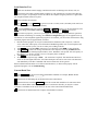
from the socket side, and secure them hand-tight only with the brass nuts as shown in Figure 1 (A).
SOLDER
(A)
(B)
Figure 1
Clamp J1 into a padded vise with the brass nuts facing up. An alternative is to temporarily attach J1 to
the K2 top cover in its intended location, labeled "AUX I/O." Either method will hold J1 firmly while
soldering in the next step.
Solder the brass nuts to the D-connector (J1) at the locations shown in Figure 1 (B). This is best
accomplished by using the tip of your soldering iron to heat both the nut and flat portion of J1 at the same
time. If you cannot melt solder onto the brass nut after heating this junction for about 8-10 seconds, use a
larger iron. Avoid overheating the connector, which could melt the plastic surrounding the solder cups.
3
Allow J1 and the brass nuts to cool, then remove the assembly from the vise.
Carefully remove the two hex standoffs. The nuts should remain firmly attached to J1. Note: If the
nuts should become loose during later assembly steps, they can be re-attached with the KIO2 in place.
Locate the larger of the two PC boards, labeled "KIO2" along one edge of the board. This is the top
side of the board. Flip the board over, so that the side with the "ELECRAFT" label is facing up.
i
In the following step, J1 may be a very tight fit onto the edge of the PC board. Press it on firmly,
but be careful not to bend any of the solder-cup pins.
Press J1 (with the nuts attached) onto the notched edge of the KIO2 board as shown in Figure 2. There
must be no gap between J1's plastic body and the edge of the board. The bottom side of the board has four
pads, corresponding to the row of 4 pins on J1. The other side has 5 pads, matching J1's 5-pin row. Each
solder-cup pin should be lined up as closely as possible with the center of its pad. Do not solder yet.
Figure 2
Note: If you have a padded vise with wide jaws, such as a PC board vise, you can use it to hold J1 firmly
against the edge of the PC board.
Make sure J1 is perpendicular to the board before soldering. Solder just one pin to its corresponding
pad, using a minimum of solder.
Re-check the position of J1. It must be pushed all the way on, and should be perpendicular to the
board. Then solder the remaining pins of both rows.
Install D1 (1N4148) on the bottom side of the board, pre-forming the leads to fit the given location.
The cathode end of the diode, which has a band (or the widest band), must be oriented towards the
banded end of the component outline. Solder D1, using a soldering time of about 1-2 seconds per lead.
Trim D1's leads as short as possible on the top side of the board after soldering.
Install D2, D3, and D4 in the same manner as D1. Note: D2's banded end faces the opposite
direction of the other three diodes.
4
Install C14 (56 pF), located near the "ELECRAFT" label. It must be seated as far down onto the PC
board as it can go, with no lead length exposed between the capacitor body and the board. Small
capacitors are fragile. Do not pull on the leads, and keep soldering time to about 1-2 seconds per lead.
Install electrolytic capacitor C8. Orient the capacitor's positive lead towards the (+) mark near the
component outline. C8 must be fully seated on the board before soldering.
Install R1 (3.9 k, ORG-WHT-RED) and R2 (47 ohms, YEL-VIO-BLK).
Install crystal X1. Make sure it is flat against the board before soldering. Use a minimum of solder.
Locate the ground pad near X1, identified by a small arrow between X1's leads on the top side of the
board. Insert a discarded component lead through this pad, then fold it over the top of X1. Solder this lead
at the ground pad, then solder it to the crystal can. Avoid overheating the crystal.
Install the capacitors listed below on the top side of the board. When soldering, be very careful not to
touch adjacent components.
__ C1, __ C2, .001 µF (102)
__ C3, __ C4, __ C5, __ C6, __ C7, __ C9, __ C11, __ C13, .01 µF (103)
__ C10, 120 pF (120 or 121)
__ C12, __ C15, 0.1 µF (104)
Install the RF chokes listed below. These miniature RF chokes are very fragile. Do not pull on the
leads, and keep soldering time to a minimum.
__ L1, 15 µH (BRN-GRN-BLK)
__ L2, __ L3, __ L4, 100 µH (BRN-BLK-BRN)
i
Touch a grounded, unpainted metal surface before handling ICs or transistors.
Install U1 (MAX1406CPE or LT1039CN16). The notched or dimpled end of the IC must be aligned
with the notched end of the component outline (pin 1 can be identified by the round pad on the PC board).
There is no need to trim the leads of U1.
Install Q1 (J310) and U2 (78L05), but do not solder yet.
Verify that Q1 and U2 are mounted in the correct locations, then solder.
5
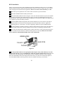
Wind 12 turns of #26 red enamel wire (7", 18 cm) on the FT23-43 toroid core (L5) as shown in Figure
3. Avoid scraping the wire against the core as you wind. The turns should occupy 80-90% of the core.
Figure 3
Trim the leads of L5 to about 1/2" long. Remove all of the enamel coating to within about 1/16"-1/8"
of the core, using a soldering iron to heat-strip the thermaleze wire. (An alternative is to use sandpaper.)
Tin the leads, and make sure they appear clean and shiny.
Install and solder the toroid vertically as indicated by L5's component outline.
On the top side of the board, to the left of C7, you'll find a small arrow. This arrow identifies a pad for
use in grounding the case of J1 (the DB9 connector). Insert a discarded component lead into this hole from
the top side of the board, then solder it at this pad.
Fold the free end of this ground lead over the top of the DB9 connector case, keeping it well away
from J1's pins. Solder the ground lead to the DB9 case. Trim excess lead length on both sides of the board.
AUX2 PC Board Assembly
Locate the smaller PC board, labeled "AUX2" on the bottom side.
On the top side of the board, install the following components:
__ C1 (0.1 µF, "104")
__ C2 (.01 µF, "103")
__ L1 (15 µH, BRN-GRN-BLK).
On the bottom side, install J1, a 10 pin female connector. Make sure J1 is flush with the board, then
solder one pin only on the top side.
If J1 is not flush with the board, re-heat the soldered pin while pushing down on the connector.
Solder the remaining pins of J1.
On the top side, install P1 (10-pin male connector). Make sure it is flush with the board, then solder.
6
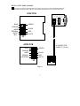
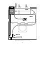
KIO2 to AUX2 Cable Assembly
Locate the 8-conductor shielded cable. This cable will be used to connect the KIO2 board to the
AUX2 board as shown in Figure 4. Refer to this illustration during the next several assembly steps.
KIO2 PCB
J2
J1
U1
BLUE
ORANGE
BARE
RED/BLK
WHITE/
BLK
J2
GREEN
BLACK
RED
WHITE
J2
AUX2 PCB
8-CONDUCTOR
CABLE, 9" (23 cm)
GREEN
BLUE
ORANGE
BARE
BLACK
RED
RED/BLK
WHITE/BLK
WHITE
J2
P1
Figure 4
7
J2
Cut a 9" (23 cm) length of the 8-conductor cable. Note: 2 feet (60 cm) of the 8-conductor is supplied.
The extra cable can be used to make a replacement if the original becomes damaged.
Carefully remove 3/4" (2 cm) of the outer gray jacket from the cable. To avoid nicking the individual
conductors, proceed slowly, using a sharp tool to cut around the circumference of the jacket. It is OK to cut
through the foil shield, which will be discarded.
Peel off and discard the thin foil shield surrounding the individual wires.
i
In the steps that follow you'll be removing insulation from all wires in the cable. If you
attempt to hold the individual wires with long-nose pliers during stripping, you may damage their
insulation or pull the wires out of the jacket. An alternative method is given in the following step.
Temporarily make a single knot in the middle of the 8-conductor cable. It should look like a pretzel,
with a diameter of about 1" (2.5 cm). The knot will apply tension to keep the wires from slipping out.
Choose any one of the eight insulated wires. Carefully remove 3/16" (5 mm) of insulation from one
end. Avoid nicking the stranded copper wires with the stripping tool.
Tightly twist the exposed strands of this wire together, then tin the strands using a very small amount
of solder. Use just enough to keep the wires from coming unraveled. Any more than this may make the
wire impossible to insert into the hole provided on the PC board.
Test the wire you just prepared to see if it will fit into one of the holes provided on the KIO2 board, at
J2. If it does not fit, you either did not twist the strands together cleanly, or you applied too much solder.
Strip 3/16" (5 mm) of insulation from each remaining insulated wire, at both ends of the cable.
Twist and tin the strands of each wire as you did above.
Twist and tin the strands of the bare wire. As with the other wires, use a minimum of solder.
Untie the knot in the cable.
If a small vise is available, clamp the KIO2 board into it in the orientation shown in Figure 4.
Otherwise you can lay the board on your work bench. Be careful not to damage crystal X1 or other
components when clamping the board into a vise.
i
CAUTION: Before proceeding, make sure you have the KIO2 board in the orientation
shown: J2's label and outline should be to the left, and the DB9 connector should be to the right. A
connector will not be used for J2; the wires will be soldered in place.
The RED and RED/BLK wires in the cable, as well as the WHITE and WHITE/BLK wires,
may be confused during assembly because the black stripes on the RED/BLK and WHITE/BLK wires are
not very prominent. To avoid confusing the striped and non-striped wires, separate out the striped wires
only and mark them with a heavy black dot using a felt pen.
8
Using long-nose pliers, insert the wires of one end of the cable into the holes of J2 on the top side of
the KIO2 board (Figure 4). Insert the wires in this order: BLUE (pin 1--round pad), GREEN (2),
ORANGE (3), BARE (5), BLACK (6), RED/BLACK (7), RED (8), WHITE/BLACK (9), WHITE (10). Be
sure to match the wire colors to their associated pads as shown. Note that the dual-row connectors have
their pins numbered left to right and top to bottom, which is different from IC pin numbering.
Turn the KIO2 board over. Bend the wires slightly so they won't fall out. Solder the wires (about 1-2
seconds per wire--excessive heat could damage the insulation). Trim off excess lead length.
When all wires are soldered, examine the solder joints carefully. All joints should be clean and shiny,
with no solder bridges.
Clamp the AUX2 PC board into a vise or place it on the work bench, using the exact orientation
shown in Figure 4. Connector P1 should be at left, and the pads for J2 should be at right. A connector will
not be used at J2. As before, the wires will be soldered into position here.
Insert the wires of the free end of the cable into the holes of J2 on the AUX2 board (Figure 4). Insert
the wires in the same order as you did on the KIO2 board: BLUE (pin 1), GREEN (2), ORANGE (3),
BARE (5), BLACK (6), RED/BLACK (7), RED (8), WHITE/BLACK (9), WHITE (10).
Turn the AUX2 board over. Carefully solder and trim the wires. Note: The wires must be trimmed as
close to the bottom of the AUX2 board as possible. This will prevent shorting to the voltmeter connector on
theK2 Control board.
Once all wires are soldered, check for (and correct) any cold solder joints or solder bridges.
K2 Control Board Preparation
Make sure the K2's power is turned OFF. If the battery is installed, put its switch in the OFF position.
Remove the 6 top cover screws shown on page 77 of the Rev. C K2 manual (Figure 7-6). Carefully lift
off the top cover and set it to the right, being careful not to short the battery terminals to the case (if
applicable). Disconnect the speaker and all top-cover option connectors.
i
If you have both the KBT2 (internal battery) and KAT2 (ATU) options installed, you should
make sure that their 2-pin connectors are visually distinguished in some manner. Otherwise, you
might reverse them during re-assembly, damaging one or more components. As of this writing, the
KBT2 12V connector was to be replaced with a different type of connector. If your KBT2's 12V connector
is the same type used for the KAT2 RF connector, you should use paint, nail polish, tape, or labels of some
type to make the two connectors easy to tell apart. For example, you could dab red model paint onto both
the male and female KBT2 12V connectors.
i
Touch a grounded, unpainted metal surface before handling the Control board in the
following steps.
9
Remove the screws that hold the Control board to the Front Panel board. If you have the KAF2 audio
filter installed, it must be unplugged first (after removing the screw on the left side).
Extract the Control board using the long-handled Allen wrench (see page 40 of the K2 manual).
If you received the revision 2.01 (or later) K2 firmware as an upgrade, and have not yet installed it,
you should do so now. Follow the steps in the K2 Revision 2 Firmware manual.
Locate 2-pin connector P5, in the upper left-hand corner of the Control board near switch S1 (top side
of the board). Trim 0.1" (2.5 mm) off both pins of P5. This will prevent shorts to the AUX2 board.
Locate the Control board revision letter, at the bottom right-hand corner near P3 (top side of the
board). If your Control board is rev. A (or XC, used during K2 field test only), you will need to modify it.
(If your board is rev. B or later, skip the next four steps.) Figure 5 shows the bottom side of the Control
board, where most of the modifications will be made. One trace will be cut (on the top side of the board).
Jumper, 4"
Cut trace on top side
P4
1
U8
.001 µF
25
Q5
40
U6
1
Jumper, 3/4"
(to pin 4 of U8,
not to RP7)
B ottom view of Control b oard
Figure 5
The trace between Q5-gate and U6 pin 25 must be cut as shown above. This trace is located on the
top side of the Control board. Once you have located the trace, use a sharp tool such as an X-acto knife to
make two small cuts near the location marked with an "X". Press down with the tip--don't draw the knife
across the trace, since you may slip, cutting adjacent pads or traces. Next, pry up and remove the small
segment between the cuts. Examine the trace closely to make sure the cut segment is completely removed.
Cut a 3/4" (19 mm) length of the supplied green-insulated hookup wire, and remove 1/8" (3 mm) of
insulation from each end. Solder this jumper on the bottom of the board, between Q5-gate and U8 pin 4, as
shown above. Make sure the jumper doesn't contact adjacent pads or component pins.
Solder a .001 µF capacitor ("102") across P4, pins 1 and 5. (Listed as Ctxd in the parts list.)
Prepare a 4" (10 cm) jumper using the green hookup wire. Solder it between U6 pin 25 and P4 pin 1
on the bottom side of the board (pin 1 is the round pad). Make sure the jumper doesn't touch adjacent pins.
10
Initial Tests
Re-install the Control board, and plug in the KAF2 module if applicable.
Plug the AUX2 board into the K2 Control board at P4 (the Aux I/O connector) as shown in Figure 6.
When the AUX2 board is correctly installed, it will be about 0.1" (2.5 mm) below the top edge of the
control board. Do not proceed until the AUX2 board is correctly installed, with all 10 pins mated.
CABLE TO KIO2 BOARD
S1
P1
AUX2 BOARD
J2
J1 ON AUX2 BOARD
PLUGGED INTO P4
ON CONTROL BOARD
U6
K2 CONTROL BOARD
Figure 6
Lay the KIO2 board over to the right side of the K2 so that it cannot contact the chassis.
Turn on the K2. If you see or smell smoke, or if the K2 does not turn on, turn power off and refer
to Troubleshooting.
The sidetone may not be working at this point, due to the Control board modifications. Tap M E N U
and locate the S T L (sidetone volume) menu entry, then hold E D I T to edit the parameter. Tap D I S P L AY
to change the sidetone source to U 8 - 4 (default is U 6 - 2 5 ). Use headphones or speaker to verify that the
sidetone can be heard. Then tap M E N U twice to return to the frequency display.
Set up a voltmeter for DC volts. Connect the (-) lead of the meter to K2 ground. Touch the (+) lead to
pin 8 of U1 on the KIO2 board. You should see a negative voltage reading of between -6 and -12 VDC.
Turn off the K2, but leave the KIO2 connected to the Control board.
11
K2 to Computer Cable Assembly
i
CAUTION: Do not use a pre-assembled cable of any kind (printer cable, etc.) between the
KIO2 and a computer. Some pins on the KIO2 provide special signals not intended for use with an RS232 interface, and you could damage the K2, KIO2, or the computer if these lines are used incorrectly. You
must assemble your own K2-to-computer cable as explained below.
Locate the 4-conductor cable. The cable can be cut to a shorter length if desired, but it will work
equally well at its full length (15', 3 m). If a longer cable is needed, contact Elecraft. Any cable substituted
for the supplied type must be shielded to minimize noise pickup.
Remove 1/2" (12 mm) of the jacket from the cable. Be very careful not to nick the individual wires.
Peel back and cut away the foil shield.
The white wire will not be used for serial communications, but should be saved as a spare. For now,
fold the white wire against the cable jacket at both ends, and secure it with small strips of tape.
Strip off 3/16" (5 mm) of insulation from each insulated wire.
Twist the strands of each wire tightly together, then tin the ends, using a minimum of solder.
Locate the DB9F (female) and DB9M (male) D connectors. Arrange them as shown in Figure 7,
with the female connector on the left and the solder cups facing up.
Each connector has a 5-pin row and a 4-pin row. Make sure the 5-pin rows are facing each other.
Figure 7 shows how the two connectors will be wired in the following steps.
Clamp the DB9F (female) connector into a padded vise, if available. This will make wiring easier.
As shown in Figure 7, pins 7 and 8 of the female connector can be wired together (using a discarded
component lead) to provide RTS/CTS loop-back1. Some application software requires this hardware
handshaking between the computer and K2. We recommend that you make this connection, unless you're
sure that your application software does not need it. Some programs use these lines for other functions,
such as CW keying of the transceiver. (If you have an existing computer-control installation, check the
present connector wiring to see if RTS/CTS loop-back can be omitted.)
Clip the bare shield wire off at the PC end of the cable only. The shield wire will be connected only at
the K2 end.
1
RTS = Request to send, CTS = Clear to send.
12
Solder the RED, GREEN, and BLACK wires of the PC end of the cable (the end with no shield wire)
to the female connector. Refer to Figure 7.
Remove the female connector from the vise, and insert the male connector. Keep this connector in the
orientation shown below.
Solder the BARE (shield), RED, GREEN, and BLACK wires to the male connector as shown.
Remove the male connector from the vise.
PC END
(FEMALE)
*
K2 END
(MALE)
BARE
1
2
RED
RED
3
4
GRN
GRN
5
BLK
1
2
3
4
5
* RTS/CTS LOOPBACK (SEE TEXT)
BLK
Figure 7
Locate the connector housings (backshells). Open the bags and remove all hardware. Each backshell
consists of two plastic halves, two long jackscrews, a small cable clamp, and associated hardware.
Attach a backshell (two halves) to one of the D connectors as shown in Figure 8. Use the provided
cable clamp to hold the cable in the proper position, then secure the clamp with two small screws. The two
jackscrews must be retained in position by the shells when the two halves are joined. Secure the backshell
halves with the provided hardware. Once this is completed, attach a backshell to the other D connector.
JACK SCREW
CLAMP
BACK SHELL
Figure 8
13
Serial Interface Test
Make sure the KIO2 board is hanging outside the K2 and is not shorting to the cabinet, tools, etc.
Connect the serial cable to the K2 and the computer. If your computer has a 25-pin serial connector,
you'll need a 9-pin to 25-pin adapter. Secure the cable at the computer using the jackscrews. Tighten them
just enough to hold the connector in place.
Turn on the K2 and computer.
Tap M E N U , then tap D I S P L AY to gain access to the secondary menu. (Secondary menu entries are
described in the K2 Revision 2 Firmware manual.)
Locate the P O R T menu entry using the B AN D + and B AN D - switches. To edit the parameter, hold
E D I T , then change it from O F F to O N (using B AN D + / B AN D - ). Tap M E N U twice to exit.
For initial test purposes, you can use your logging or control program to verify that basic operations
such as band or mode change are working. (See Software Configuration, page 18, for application set up
information.) If a K2-compatible application program is not available, you can test the serial interface using
a terminal program such as Hyperterminal, as follows:
1.
2.
3.
4.
5.
Run the terminal program. Set it up for communication at 4800 baud, with 2 stop bits (1 will also
work), 8 data bits, and no parity. Turn off hardware handshaking (RTS/CTS). It's also helpful to turn
on local echo and line-feed so you can see what you're sending to the K2.
Tap M E N U and locate the P O R T menu entry as you did earlier. Hold E D I T to enter edit mode.
Tap D I S P L AY to send a test message from the K2 to the computer. The string FA000xxxxxxxx;
should be seen in the terminal program window, where xxxxxxxx is the present VFO A frequency in
Hz. (The first "x" will be 0 if VFO A is set to a frequency below 10 MHz.)
Tap M E N U twice to exit the menu.
At the computer keyboard, type SW01; (the semicolon is required). This should cause the K2 to
switch to the next higher band. Note: You cannot backspace and correct errors since each character is
sent immediately to the K2. Commands with incorrect characters will be ignored.
If the K2 did not transmit and/or receive data as described above, or did not work properly with an
application program, refer to Troubleshooting.
Current Drain Test
Tap D I S P L AY and check current drain with the KIO2 installed. For example, E 1 3 . 8 i 0 . 2 2
indicates 0.22A. Your reading: __________ A.
Turn the K2 off and unplug the AUX2 board from the Control board.
Turn the K2 back on and tap D I S P L AY again. The current drain should now be 0.00-0.02A lower
than it was with the KIO2 connected. If the difference is much more than this, you may have a short
somewhere on the KIO2 or the AUX2 board, or an error in the Control board modifications.
Turn the K2 off and disconnect the computer from the KIO2 connector.
14
KAT2
KIO2
PCB
KBT2
ATU-J7
ATU-J8
AUX2 PCB
Figure 9. KIO2 installation in top cover (see text).
15
KIO2 Installation
Figure 9 (previous page) shows where the KIO2 board will be installed in the K2's top cover. The KIO2's
female D connector will be mounted in the hole labeled "AUX I/O" on the rear panel. The ATU's control
cable will plug into the AUX2 board (if applicable). There is no need to remove the battery or ATU.
Place the top cover upside down on a cloth or other soft surface to protect the finish.
Disconnect the KIO2/AUX2 assembly from the K2.
Position the KIO2 module as shown in Figure 9. The side of the board with the crystal (X1) should be
facing up; the side with the cable connections faces down. If you have the module placed correctly, the
female connector will be aligned with the trapezoid-shaped AUX I/O panel hole. Note: The module may be
a very tight fit if you have the battery installed.
Secure the KIO2 module using the hex male-female standoffs. Do not use washers of any kind, as
they will prevent the serial I/O cable from being fully inserted into the KIO2 connector. Tighten the
standoffs using pliers or a socket driver. Avoid over-tightening, which may strip the standoff threads.
If a battery (KBT2) is installed, route the 8-conductor cable around it as shown. If an ATU (KAT2) is
installed, position its RF cable as shown, and make sure this cable is not shorting to the KIO2 board.
If you have the antenna tuner installed, plug its control cable into P1 on the AUX2 board as shown in
Figure 10. Orient the ATU connector as shown, with the green wire at the top. Make sure the antenna
tuner's connector is mated with all 10 pins of P1 on the AUX2 board.
GREEN WIRE
AUX2 PCB
TO KAT2
TO KIO2
Figure 10
Use the provided cable ties to keep all option cables in place. If any of the cables lay across the
RF board once the top cover is re-installed, they could cause spurious signals in the receiver. The best
location for the cable ties depends on which options you have installed. If you have a battery installed,
make sure that the KIO2 cable runs along the side of the battery, just above the 2-D fastener (Figure 9).
You can bundle the KIO2 cable along with the red wires running to the battery on/off switch.
16
i
Place the top cover to the right of the K2, on its right edge, while plugging in cables in the
following steps. It may be helpful to place a 2-3" stack of books at the right side of the K2 as a support for
the top cover. Be very careful not to short the battery terminals to the chassis.
Plug in the speaker connector.
Plug the AUX2 board assembly into the K2 Control board. Make sure the AUX2 board is oriented as
shown in Figure 6.
i
Review the comments at the bottom of page 9 regarding the ATU and battery connectors.
Plugging them in at the wrong locations on the RF board can damage one or more components.
If you have an ATU (KAT2), plug its RF cable into the K2 RF board connector labeled "AUX RF".
If you have an internal battery (KBT2), plug its cable into the K2 RF board connector labeled "AUX
12V".
Place the top cover onto the K2 carefully, adjusting the positions of cables as needed. Re-install the
top cover hardware (six screws).
If a battery is installed, set its slide switch to the ON position if required.
This completes assembly and installation of the KIO2.
17
Computer Control Using the KIO2
Computer, Antenna, and Noise Considerations
Desktop computers and their peripherals--especially monitors and networking equipment--can generate
spurious signals over wide portions of the HF spectrum. If your antenna is fed with coax, you may not hear
any computer-generated noise at all. However, if you use an end-fed random-wire antenna that's connected
directly to the transceiver, or use unshielded feedline (twin-lead, ladder line, etc.) you'll almost surely hear
birdies or hash on some bands when the computer is on. Even if the computer is not being used for
communication with the K2, its RFI may be heard on quiet bands.
If computer-generated noise is a problem at your QTH, you may have to improve your ground system, reorient your antenna(s), move the antenna(s) farther away, or use coax feed. When you're only using the
computer to control the transceiver, you may be able to turn off networking equipment and switching
power supplies, which are the worst offenders.
Some types of weak, computer-modulated noise heard on quiet bands can be reduced in amplitude by
disabling the KIO2's on-board crystal oscillator. The negative supply voltage is then derived from the
computer's "RxD" signal. This alternative is described in the Troubleshooting section.
Software Configuration
The KIO2 is intended to be compatible with a wide range of existing PC-based logging, DXing, remote
control, and contesting applications. However, we cannot guarantee 100% compatibility. Some applications
have been (or will be) modified by their developers to take advantage of the K2's full command set.
In general, software used with the K2 should be set up as follows:
Radio Type:
Interface:
Handshaking:
Polling:
TX Polling:
Elecraft K22
4800 baud, 8 data bits, no parity, 2 stop bits (1 stop bit will also work)
Set to "None" if this choice is provided. No hardware handshaking is required.
Many programs periodically poll the radio to see if the operator has manually
adjusted any of the controls. The K2 can respond very quickly to these requests, but
we recommend a setting of 1-3 seconds to minimize possible computer noise.
Polling during transmit is allowed, but we recommend turning it off.
Table 1 (page 19) may provide further details about using your software with the K2. Check our web site
for more up-to-date information. Also available on the web is the Elecraft KIO2 Programmer's Reference,
which you can consult when writing your own K2 control programs.
2
If your software does not list the K2, select the TS-570D or the closest equivalent (950, 850, 50). The K2 can
recognize a large subset of TS-570 commands. (TS-570 is a trademark of the Kenwood Corporation.)
18
Table 1. Application software information.
Program
CT
DX4WIN
K2REMOTE, K2VOICE
Log-EQF, Rig-EQF
MixW
NA
RCP570
T-R Log
TRX Manager
WriteLog
YPLOG
K2 Configuration and Operating Notes
DOS program; requires a batch file to start up correctly (for details see
http://www.k1ea.com/hintkink.htm). In the batch file, use the command
COMTSRx -Px -B4800 -N82 (e.g., x = 1 for COM1)
Set Radio 1 to TS950 if K2 is not in the list. Optional: change bands from
the K2 manually the first time so CT can store the values for VFO A and
VFO B for each band (*). You can then change bands from the PC or K2.
Use Kenwood (generic) radio type, 4800 baud. Default polling rate is
6000 msec with 6 retries, but 1000-2000 msec is recommended. Clicking
on a DX spot may set the wrong mode, due to the order in which the
program sends the mode and band-change commands (*). If you use
"scanning" mode, don't set it up to scan multiple bands, since this could
cause excessive K2 relay wear, especially if unattended.
See descriptions on page 20.
A modified rig file for these programs that better supports the K2's
RTTY and RTTY-reverse modes can be found on our web site.
Ver. 2.02 and later includes K2 support (may be listed under Kenwood).
Run the "CONFIG" program. Select F4 (Serial Port Setup).
On the desired port, set baud to 4800, and set device to XCVR1.
Select F5 (Equipment Configuration). Set XCVR #1 to KENWOOD1
Run NA. Go to the Equipment Control Panel and check Radio #1.
TS-570 emulation; some controls not applicable to the K2. Since the K2
supports only a subset of TS570 commands, the program will time out on
the others, and can take up to 30 seconds to turn on the radio display on
start-up. Don't use SEND button (hangs the computer).
Ver 6.63 includes Elecraft K2 as a radio type.
For older versions, in the configuration file (.cfg), set:
RADIO ONE TYPE = TS570
Also add SHIFT KEY ENABLE = TRUE to use the right and left
SHIFT keys to change the receive frequency when RIT is on. Hitting
both shift keys simultaneously resets the RIT to zero.
RTS/CTS loop-back required at computer end (pin 7 to pin 8).
Check the "Poll" box, and select No for "Comm PTT".
Specify 2-wire mode (RxD/TxD, no handshaking). The program may
send the K2 "FL" filter selection commands, which are not supported.
(*) These issues are likely to be resolved once full K2 support is added by the program's developer.
19
Using the K2REMOTE and K2VOICE Programs
K2REMOTE provides flexible remote control of the K2, even over the Internet (using TCP/IP).
K2VOICE is a voice feedback program for the K2 which make the K2 fully usable by hams who are unable
to see the normal K2 controls and displays.
Both of these programs were developed by Elecraft for use with the KIO2. You can download the programs
and associated documentation from our web site.
CW Keying and PTT
There are three basic ways to key the K2 when using a computer:
1.
Directly-connected microphone, hand key, paddle, etc.: This is the simplest method, and may be
preferred if you don't plan to use the computer to generate CQs and contest exchanges, etc.
2.
Serial or parallel-port control line keying: Most programs support this method. In SSB mode the
computer turns a selected control line on to activate PTT. In CW mode, the computer generates the
dots and dashes, turning the selected control line on and off in response. The control line(s) used-which may be at RS-232 or TTL/CMOS levels--must be level-shifted for connection to the K2 key
and/or mic jacks.
3.
"Virtual" keying, using computer commands sent to the KIO2's serial port: In this case, no
connection to the key or mic jacks is required for keying the K2. In SSB mode, the computer sends the
K2 "TX" and "RX" commands, which the K2 responds to by turning PTT on and off internally. In CW
mode, the computer sends typed characters to the K2 using a "KY" command, and the K2 converts the
characters to dots and dashes internally. This method of keying is supported by only a few remotecontrol applications, including RCP570 and Elecraft's K2REMOTE program. (For details on the TX,
RX, and KY commands, refer to the KIO2 Programmer's Reference.)
Case (2) above is by far the most common. Connection diagrams showing how to use serial or parallel port
control lines are usually provided in the program's user manual.
In the case of a serial port control line, you can use the spare wire (white) in the 4-conductor cable for CW
or PTT keying. You'll need to connect this wire to the specified control line at the PC end. At the K2 end, a
simple level converter using an NPN transistor will be required (usually diagrammed in your program's
user manual). The white wire must then be brought out from the connector at the K2 end and routed to a
1/8th inch stereo plug for the key jack. You can optionally use two diodes (or two transistors) to take
advantage of the K2's "auto-detect" feature, allowing both the computer and a keyer paddle to be connected
to the K2's key jack at the same time.
Additional information on this topic can be found on our web site.
20
Connecting Other Equipment to the KIO2
The KIO2's 9-pin connector provides a number of signals in addition to those needed for the RS-232 serial
interface (Table 2). Note: Use pin 1 as the electrical ground for any external devices. Pin 5 should only be
used as the RS-232 ground return to the computer.
Table 2. KIO2 Signal Descriptions.
J1 Pin
1
2
3
4
Signal Description
Chassis Ground
TxD
RxD
ALC
5
6
RS-232 Sig. Ground
AuxBus
7
RF Detect
8
DC Supply Voltage
9
8 V Receive
Notes
RF/DC ground (use pin 5 for RS-232 signal ground)
RS-232 data from K2 to computer (RF filtered)
RS-232 data from computer to K2 (RF filtered)
Automatic Level Control from an external amp to the SSB
adapter. Refer to our web site for related application notes.
RS-232 ground return (for computer serial data; RF filtered)
K2 configuration network (RF filtered), intended for use
with external AuxBus-compatible peripherals. Connections
made to this line must be shielded, and total bypass
capacitance should be between .001 and .005 µF. Excessive
capacitance may cause auxBus data transmission errors.
RF level feedback (DC), intended for use with external
SWR bridges (when a KAT2 is not installed). A lowimpedance (< 100 ohms) DC signal driving this line will
override the K2's internal RF detector. Refer to the KAT2
ATU schematic for an example. Improper use of this line
could result in incorrect K2 power settings, high current, etc.
This is intended as a power-on signal from the K2, and/or
for powering low-current external peripherals. Total load
current should be kept under 50 mA continuous, 80 mA
peak to avoid damage to L1 on the AUX2 board. A 150-Ω
or larger series current limiting resistor should be used.
Bypass capacitors in external equipment must be placed on
the far end of the limiting resistor (i.e., not on the K2 end).
8 V on receive, 0 V on transmit (approx.), current-limited to
2 mA. This signal is intended for use sequencing external
amplifiers. A new firmware feature allows the 8 V receive
line to remain low during the entire T - R delay to reduce
CW-mode relay switching. See the K2 Rev. 2 Firmware
manual for further details.
21
Troubleshooting
If your symptoms are not covered below, check the orientation of all components, connectors, and wiring;
look for cold solder joints; and check all DC voltages (see DC Voltage Chart).
Band changes take longer than before: This is completely normal, and has nothing to do with the KIO2.
The new K2 firmware (revision 2.01 or later) suppresses relay switching during rapid band changes. The
receiver will come alive about 1/2 second after the last tap of B AN D + or B AN D - .
No KIO2 to computer data communication: Usually this is caused by a broken or poorly soldered I/O
connection, or by incorrect setup of the computer program. Verify the baud rate (4800) and related settings
at the computer, and make sure the P O R T menu entry in the K2 is set to O N . Your software may require
the CTS/RTS loopback shown in Figure 7. Also, some PC programs work only under DOS or require extra
serial port configuration steps. Check our web site for further information about your software or PC.
No characters are echoed when typing using Hyperterminal: There is a bug in some versions of
Hyperterminal that prevents local character echo even if the appropriate box is checked. A link to a
corrected version or patch may be available on our web site.
Missing sidetone: The Control board modification, which was made to improve RS-232 interface
performance, changes the source of the sidetone to pin 4 of U8. The original sidetone source, pin 25 of U6,
becomes the serial transmit pin. The K2 needs to be configured to recognize the new sidetone source as
explained on page 11. If the sidetone still can't be heard, re-check all Control board modification steps.
No (-) supply voltage at U1-8: The KIO2's crystal oscillator may not be running. This oscillator operates
at about 16.29 MHz. Most K2's can tune to this frequency, where you can hear the KIO2's signal. First,
switch to the 17-meter band (18 MHz). Next, tune the VFO to the KIO2's oscillator frequency; the signal
should be loud and stable. If you can't find the signal, it may be because your K2's VFO cannot tune this
low in frequency. Try looking for the KIO2 oscillator signal using a general-coverage receiver, with a short
length of wire as an antenna (drape the wire near the KIO2). If you still can't find the signal, proceed with
the DC voltage checks.
Strong noise signals heard on one or more bands: This could indicate that the KIO2's 8-wire cable, or
another option cable, is laying directly on top of the K2's RF board. Remove the top cover and re-dress the
cables using cable ties. It may actually be easier to remove the right side panel for this purpose, since you
can see exactly how all of the cables are positioned with the top cover in place.
Weak noise signals heard on quiet bands: It's nearly impossible to eliminate all computer-related noise.
However, you may be able to eliminate some weak, computer-modulated signals heard on quiet bands. This
involves disabling the KIO2's on-board 16.29 MHz crystal oscillator. If you disable the oscillator, the (-)
supply voltage for the KIO2 is then derived from the computer's "RxD" signal at pin 3 of J1 (on the KIO2
board). This will not work in all cases, since some computers don't provide an adequate voltage level on the
RxD line.
To disabled the oscillator, remove R2 on the KIO2 (47 ohms). Do before and after tests on the suspected
noise signal to verify that this eliminates it. Then test the KIO2 with the software application to make sure
it still functions correctly. Do this with each computer to be used with the K2.
22
DC Voltage Chart
These measurements were made with a 14 V power supply, R2 installed, and no computer or other external
equipment connected to J1 on the KIO2. Negative voltages may vary by +/- 3V or more without affecting
performance. Voltages marked with an asterisk (*) may vary due to DMM probe loading effects.
Pin
V
Pin
V
Pin
V
Pin
V
Pin
V
Pin
V
Pin
V
J1-1
J1-2
J1-3
J1-4
J1-5
J1-6
J1-7
J1-8
J1-9
0
-8
0.1
4.5
0
5.5
0
14
8
U1-1
U1-2
U1-3
U1-4
U1-5
U1-6
U1-7
U1-8
U1-9
14
0.1
14
0.1
-8
0.1
14
-9
0
U1-10
U1-11
U1-12
U1-13
U1-14
U1-15
U1-16
0
5
5
4.5
0
4.5
5
J2-1
J2-2
J2-3
J2-4
J2-5
J2-6
J2-7
J2-8
J2-9
5.0
5.5
5
0
0
0
4.5
14
8
J2-10
0
U2 in
Out
14
5
Q1-G
Q1-S
Q1-D
-1*
0*
14
D3-A
D3-C
D4-A
D4-C
-4*
0
-1*
5
D1-A
D1-C
D2-A
D2-C
-9
0.1
-9
-4*
Circuit Details
Refer to the schematic diagram, page 24.
U1 is an RS-232 transceiver IC. It converts the 5V logic-level signals at pins 11 and 12 (RX and TX data)
to RS-232 levels, typically +/- 5 to +/- 12 VDC. Q1 is a Colpitts oscillator that drives a negative-going
detector (D2/D3). The negative voltage is filtered by C8 and supplied to U1 (pin 8) as the (-) transmit
supply voltage (Vss). L2-L4 and C3-C6 provide pi-net RF filtering. The RS-232 signal ground (J1, pin 5) is
isolated from the chassis ground (pin 1) to reduce noise pickup.
If the on-board crystal oscillator is disabled by removing R2, the negative supply voltage (U1 pin 8) is
derived from the RxD line (J1 pin 3) rather than from the oscillator. This voltage will vary depending on
the K2's serial I/O transmit duty cycle as well as the quiescent voltage supplied by the computer on RxD. If
the on-board oscillator is running (R2 installed), the negative supply voltage will be determined by either
the RxD line or the detector output (D2/D3), whichever is more negative.
23
L2-L4: 100 µH
C3-C6: .01 µF
-6 TO -12 V
C8
D1
10 µF
D2
1N4148
+
J1
To PC
1N4148
D1-D4
1
L2
D3
2
TXD
VDD
T1IN
R1OUT
VCC
3
4
5
R1IN
R2OUT
7
T1OUT
T2IN
6
1
2
3
R2IN
R3OUT
C9
Q1
J310
D4
1N4148
C10
120
AUX
MAX1406
D
S
D
G
U1
C1
.001
Q1
.01
16
15
14
13
12
11
9
10
15µH
4
T2OUT
L1
5
R3IN
RF
12V
6
GND
T3IN
C4
T3OUT
C5 C6
12V
VSS
L4
7
C3
8
L3
ALC
8
C
1N4148
RXD
9
A
S
X1
L5
FT23-43
16.289 MHz
C11
.01
8R
C14
56
R1
3.9K
J1, BACK VIEW
1
2
3
4
R2
47
J2
5
To CTRL Board
2
4
6
8
10
/K2 RX
9
9
7
8
5
7
3
6
1
/K2 TX
ALC
8R
RF
AUX2 BOARD
C2
.001
C7 C13
.01 .01
ALL PINS OF P1, J1, AND J2 ARE CONNECTED IN PARALLEL
P1
J1
J2
To CTRL-P4
To KIO2-J2
5V
2
1
2
1
2
1
C12
0.1
OUT
IN
GND
C15
U2
3
4
3
4
3
4
5
6
5
6
5
6
0.1
OUT
IN
7
8
7
10
9
10
9
10
8
9
8
7
GND
= On bottom of PC board.
L1
12V
C1
0.1
12V
U2
78L05
EXCEPT FOR PIN 8, WHICH IS CONNECTED AS SHOWN.
To ATU-J8
AUX
15µH
Elecraft
C2
.01
By W. Burdick
E. Swartz
24
KIO2 Aux I/O Adapter
Rev.
Date
E
6-13-01
Sht.
1 of 1
G
Customer Service and Support
Technical Assistance
You can send e-mail to [email protected] and we will respond quickly – typically the same day
Monday through Friday. If you need replacement parts, send an e-mail to [email protected]. Telephone
assistance is available from 9 A.M. to 5 P.M. Pacific time (weekdays only) at 831-763-4211. Please use email rather than calling when possible since this gives us a written record of the details of your problem and
allows us to handle a larger number of requests each day.
Repair / Alignment Service
If necessary, you may return your Elecraft product to us for repair or alignment. (Note: We offer unlimited
email and phone support, so please try that route first as we can usually help you find the problem quickly.)
IMPORTANT: You must contact Elecraft before mailing your product to obtain authorization for the
return, what address to ship it to and current information on repair fees and turnaround times. (Frequently
we can determine the cause of your problem and save you the trouble of shipping it back to us.) Our repair
location is different from our factory location in Aptos. We will give you the address to ship your kit to at
the time of repair authorization. Packages shipped to Aptos without authorization will incur an additional
shipping charge for reshipment from Aptos to our repair depot.
Elecraft 1-Year Limited Warranty
This warranty is effective as of the date of first consumer purchase (or if shipped from the factory, the date the
product is shipped to the customer). It covers both our kits and fully assembled products. For kits, before
requesting warranty service, you should fully complete the assembly, carefully following all instructions in the
manual.
Who is covered: This warranty covers the original owner of the Elecraft product as disclosed to Elecraft at the
time of order. Elecraft products transferred by the purchaser to a third party, either by sale, gift, or other method,
who is not disclosed to Elecraft at the time of original order, are not covered by this warranty. If the Elecraft
product is being bought indirectly for a third party, the third party’s name and address must be provided at time
of order to ensure warranty coverage.
What is covered: During the first year after date of purchase, Elecraft will replace defective or missing parts
free of charge (post-paid). We will also correct any malfunction to kits or assembled units caused by defective
parts and materials. Purchaser pays inbound shipping to us for warranty repair; we pay shipping to return the
repaired equipment to you by UPS ground service or equivalent to the continental USA and Canada. For Alaska,
Hawaii, and other destinations outside the U.S. and Canada, actual return shipping cost is paid by the owner.
What is not covered: This warranty does not cover correction of kit assembly errors. It also does not cover
misalignment; repair of damage caused by misuse, negligence, battery leakage or corrosion, or builder
modifications; or any performance malfunctions involving non-Elecraft accessory equipment. The use of acidcore solder, water-soluble flux solder, or any corrosive or conductive flux or solvent will void this warranty in its
entirety. Also not covered is reimbursement for loss of use, inconvenience, customer assembly or alignment
time, or cost of unauthorized service.
Limitation of incidental or consequential damages: This warranty does not extend to non-Elecraft equipment
or components used in conjunction with our products. Any such repair or replacement is the responsibility of the
customer. Elecraft will not be liable for any special, indirect, incidental or consequential damages, including but
not limited to any loss of business or profits.
25