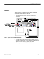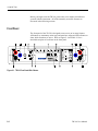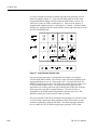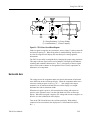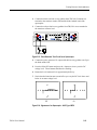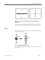
1
User Manual
TR 210 Tracker
071-0114-01
Copyright © Tektronix, Inc. All rights reserved.
Tektronix products are covered by U.S. and foreign patents, issued and pending. Information in this publication supercedes
that in all previously published material. Specifications and price change privileges reserved.
Printed in the U.S.A.
Tektronix, Inc., PO Box 500, Beaverton, OR 97077
TEKTRONIX and TEK are registered trademarks of Tektronix, Inc.
Huntron and Tracker are registered trademarks of Huntron, Inc.
WARRANTY
Tektronix warrants that the products that it manufactures and sells will be free from defects in materials and
workmanship for a period of one (1) year from the date of purchase from an authorized Tektronix distributor. If
any such product proves defective during this warranty period, Tektronix, at its option, either will repair the
defective product without charge for parts and labor, or will provide a replacement in exchange for the defective
product. Batteries are excluded from this warranty.
In order to obtain service under this warranty, Customer must notify Tektronix of the defect before the expiration
of the warranty period and make suitable arrangements for the performance of service. Customer shall be
responsible for packaging and shipping the defective product to the service center designated by Tektronix,
shipping charges prepaid, and with a copy of customer proof of purchase. Tektronix shall pay for the return of the
product to Customer if the shipment is to a location within the country in which the Tektronix service center is
located. Customer shall be responsible for paying all shipping charges, duties, taxes, and any other charges for
products returned to any other locations.
This warranty shall not apply to any defect, failure or damage caused by improper use or improper or inadequate
maintenance and care. Tektronix shall not be obligated to furnish service under this warranty a) to repair damage
resulting from attempts by personnel other than Tektronix representatives to install, repair or service the product;
b) to repair damage resulting from improper use or connection to incompatible equipment; c) to repair any
damage or malfunction caused by the use of non-Tektronix supplies; or d) to service a product that has been
modified or integrated with other products when the effect of such modification or integration increases the time
or difficulty of servicing the product.
THIS WARRANTY IS GIVEN BY TEKTRONIX WITH RESPECT TO THE LISTED PRODUCTS IN
LIEU OF ANY OTHER WARRANTIES, EXPRESS OR IMPLIED. TEKTRONIX AND ITS VENDORS
DISCLAIM ANY IMPLIED WARRANTIES OF MERCHANTABILITY OR FITNESS FOR A
PARTICULAR PURPOSE. TEKTRONIX’ RESPONSIBILITY TO REPAIR OR REPLACE DEFECTIVE
PRODUCTS IS THE SOLE AND EXCLUSIVE REMEDY PROVIDED TO THE CUSTOMER FOR
BREACH OF THIS WARRANTY. TEKTRONIX AND ITS VENDORS WILL NOT BE LIABLE FOR ANY
INDIRECT, SPECIAL, INCIDENTAL, OR CONSEQUENTIAL DAMAGES IRRESPECTIVE OF
WHETHER TEKTRONIX OR THE VENDOR HAS ADVANCE NOTICE OF THE POSSIBILITY OF
SUCH DAMAGES.
Contacting Tektronix
Product
Support
For application-oriented questions about a Tektronix measurement product, call toll free in North America:
1-800-TEK-WIDE (1-800-835-9433 ext. 2400)
6:00 a.m. – 5:00 p.m. Pacific time
Or contact us by e-mail:
[email protected]
For product support outside of North America, contact your
local Tektronix distributor or sales office.
Service
Support
Contact your local Tektronix distributor or sales office. Or visit
our web site for a listing of worldwide service locations.
http://www.tek.com
For other
information
In North America:
1-800-TEK-WIDE (1-800-835-9433)
An operator will direct your call.
To write us
Tektronix, Inc.
P.O. Box 500
Beaverton, OR 97077
Contents
General Safety Summary................................................................................ v
Introduction and Specifications .................................................................. 1-1
What is Signature Analysis?........................................................................... 1-2
Power Configuration ...................................................................................... 1-3
Signal Fuse Replacement................................................................................ 1-4
50/60Hz Selector Switch ................................................................................ 1-4
Unpacking Your TR 210 ................................................................................ 1-4
Installation ...................................................................................................... 1-5
Operating the TR 210 ..................................................................................... 1-6
Specifications ................................................................................................. 1-8
Accessories ..................................................................................................... 1-12
A Quick Tour ................................................................................................ 2-1
Front Panel...................................................................................................... 2-2
Back Panel ...................................................................................................... 2-4
Oscilloscope Display ...................................................................................... 2-5
Initial Setups ................................................................................................... 2-6
Power On ........................................................................................................ 2-6
Range Selection .............................................................................................. 2-6
Frequency Selection ....................................................................................... 2-7
Channel Selection........................................................................................... 2-7
Pulse Generator .............................................................................................. 2-8
Using Your TR 210 ....................................................................................... 3-1
Basics of ASA - How it Works ...................................................................... 3-2
Horizontal Axis .............................................................................................. 3-3
Vertical Axis................................................................................................... 3-4
Basic Analog Signatures - Open and Short .................................................... 3-5
Four Basic Component Analog Signatures .................................................... 3-7
TR 210 User Manual
i
Contents
Testing Passive Components........................................................................ 4-1
Resistors.......................................................................................................... 4-1
Shorts and Opens, Resistor Faults .................................................................. 4-4
Review ............................................................................................................ 4-4
Troubleshooting Applications ........................................................................ 4-5
Capacitors ....................................................................................................... 4-6
Capacitor Analog Signatures .......................................................................... 4-7
The Signatures of Different Capacitors in LOW2 Range............................... 4-8
Understanding Capacitor Analog Signatures.................................................. 4-9
Capacitor Failures - Leakage .......................................................................... 4-10
Review ............................................................................................................ 4-11
Applications.................................................................................................... 4-11
Inductors ......................................................................................................... 4-11
Inductor Analog Signatures ............................................................................ 4-12
The Signatures of Different Inductors in LOW2 Range................................. 4-13
Affect of Frequency Fs on Inductor Signatures .............................................. 4-13
Understanding Inductive Signatures............................................................... 4-14
Review ............................................................................................................ 4-14
Applications.................................................................................................... 4-15
Electromechanical Switching Components .................................................... 4-16
Manually Operated Mechanical Switches ...................................................... 4-16
Review ............................................................................................................ 4-18
Electomechanical Relays ................................................................................ 4-18
Relay Coil Test ............................................................................................... 4-18
Using the Pulse Generator to Test a 5V Reed Relay...................................... 4-19
Review ............................................................................................................ 4-20
Testing Discrete Semiconductors ................................................................ 5-1
Diodes ............................................................................................................. 5-1
Diode Analog Signatures ................................................................................ 5-1
Affects of Frequency (Fs) on the Diode Signature ......................................... 5-3
The Composite Diode Signature..................................................................... 5-3
Diode Failures................................................................................................. 5-4
Internal Resistance Flaw in a Diode ............................................................... 5-5
Internal Leakage Flaw in a Diode................................................................... 5-6
Zener Diodes................................................................................................... 5-6
Review ............................................................................................................ 5-8
Applications.................................................................................................... 5-8
Transistors ...................................................................................................... 5-9
Bipolar Transistor Signatures ......................................................................... 5-9
Bipolar Transistor Base-Collector Signatures ................................................ 5-10
Identifying Unknown Transistors ................................................................... 5-12
Darlington Bipolar Transistor Signatures....................................................... 5-14
Using the Pulse Generator to Test Transistor Operation................................ 5-15
Analyzing the Active Characteristics of a Transistor..................................... 5-16
Review ............................................................................................................ 5-17
Applications.................................................................................................... 5-18
Optical Switches ............................................................................................. 5-18
Phototransistors .............................................................................................. 5-19
ii
TR 210 User Manual
Contents
Optocoupler Dynamic Testing........................................................................ 5-20
Optocoupler Signatures .................................................................................. 5-20
SCRs and Triacs ............................................................................................. 5-22
Silicon Controlled Rectifiers (SCRs) ............................................................. 5-22
Active Testing of an SCR............................................................................... 5-24
Triacs .............................................................................................................. 5-25
Active Testing of Triacs ................................................................................. 5-26
Review ............................................................................................................ 5-27
Applications.................................................................................................... 5-27
Testing Integrated Circuits.......................................................................... 6-1
Digital Integrated Circuits .............................................................................. 6-1
Integrated Circuit Failures.............................................................................. 6-1
Digital Integrated Circuit Signatures.............................................................. 6-2
Signatures of a Digital IC ............................................................................... 6-3
Signatures for Different Logic Chip Families ................................................ 6-4
Comparing Two TTL Families....................................................................... 6-4
CMOS Logic Family ...................................................................................... 6-5
CMOS Components and Test Signal Frequency Fs ........................................ 6-7
Troubleshooting Digital Logic ICs................................................................. 6-8
Comparison Testing for Digital ICs ............................................................... 6-9
Review ............................................................................................................ 6-10
Applications.................................................................................................... 6-10
Analog Circuits............................................................................................... 6-11
Op Amps......................................................................................................... 6-11
Op Amp Signatures ........................................................................................ 6-12
Troubleshooting Op Amp Circuits ................................................................. 6-13
Linear Voltage Regulators.............................................................................. 6-14
Review ............................................................................................................ 6-15
Applications.................................................................................................... 6-15
Low Voltage ................................................................................................... 6-16
Review ............................................................................................................ 6-18
Applications.................................................................................................... 6-18
TR 210 User Manual
iii
Contents
iv
TR 210 User Manual
General Safety Summary
Review the following safety precautions to avoid injury and prevent damage to
this product or any products connected to it. To avoid potential hazards, use this
product only as specified.
Only qualified personnel should perform service procedures.
To Avoid Fire or Personal
Injury
Use Proper Power Cord. Use only the power cord specified for this product and
certified for the country of use.
Use Proper Voltage Setting. Before applying power, ensure that the line selector is
in the proper position for the power source being used.
Connect and Disconnect Properly. Do not connect or disconnect probes or test leads
while they are connected to a voltage source.
Ground the Product. This product is grounded through the grounding conductor of
the power cord. To avoid electric shock, the grounding conductor must be
connected to earth ground. Before making connections to the input or output
terminals of the product, ensure that the product is properly grounded.
Observe All Terminal Ratings. To avoid fire or shock hazard, observe all ratings and
markings on the product. Consult the product manual for further ratings
information before making connections to the product.
Do not apply a potential to any terminal, including the common terminal, that
exceeds the maximum rating of that terminal.
Do Not Operate Without Covers. Do not operate this product with covers or panels
removed.
Use Proper Fuse. Use only the fuse type and rating specified for this product.
Avoid Exposed Circuitry. Do not touch exposed connections and components when
power is present.
Do Not Operate With Suspected Failures. If you suspect there is damage to this
product, have it inspected by qualified service personnel.
Do Not Operate in Wet/Damp Conditions.
Do Not Operate in an Explosive Atmosphere.
Keep Product Surfaces Clean and Dry.
TR 210 User Manual
v
General Safety Summary
Symbols and Terms
Terms in this Manual. These terms may appear in this manual:
WARNING. Warning statements identify conditions or practices that could result in
injury or loss of life.
CAUTION. Caution statements identify conditions or practices that could result in
damage to this product or other property.
Terms on the Product. These terms may appear on the product:
DANGER indicates an injury hazard immediately accessible as you read the
marking.
WARNING indicates an injury hazard not immediately accessible as you read
the marking.
CAUTION indicates a hazard to property including the product.
Symbols on the Product. The following symbols may appear on the product:
vi
TR 210 User Manual
Introduction and Specifications
The Tektronix TR 210 is an accessory to an oscilloscope which allows power off
troubleshooting of electronic circuits by using the technique of Analog Signature
Analysis.
This signature shows the V/I characteristics of an electronic device which when
compared with a known good device, can assist in locating faulty components of
a circuit without applying power to the board under test. This technique of
troubleshooting simply involves the visual comparison of circuit signatures
which can assist in isolating circuit failures due to opens, shorts, device leakage,
ESD damage, power supply over-voltage and transients.
Figure 1-1. TR 210
TR 210 User Manual
1-1
Introduction and Specifications
What is Analog Signature Analysis?
Analog Signature Analysis or ASA is a unique, power-off troubleshooting
technique. It uses an alternating current (AC) sinewave stimulus to show the
current (I) vs. voltage (V) characteristic of an unpowered component on a CRT.
The IV characteristic is called an analog signature and each pin of a component
can have a unique signature. When components fail, their signatures change so
troubleshooting using ASA is simply a matter of finding the defective
component by analyzing its signature. You can compare signatures of suspect
components to signatures of known-good components.
Test current applied across a component is limited. When used carefully, this
technique is non-destructive and does not damage any components. ASA has
many advantages as a proven, fast, and effective troubleshooting technique.
You can:
1-2
■
Troubleshoot circuitry that cannot be powered up due to a shorted condition.
■
Troubleshoot in a qualitative mode, allowing you to see physical problems
with a suspect component.
■
Compare device characteristics with known types for better matching.
■
Eliminate risk of accidental shorting across other points during POWER ON
testing which could further damage the component or other components on
the board.
■
Minimize the risk of shock hazard since the ASA troubleshooting approach
requires no power applied to the circuitry.
■
Perform preventative maintenance by seeing flaws in components that could
possibly lead to untimely failures.
■
Look at replacement components before they are installed in circuitry to
reduce the risk of installing defective ones.
TR 210 User Manual
Introduction and Specifications
The Tektronix TR 210 graphically displays the analog signature when connected
to two terminals of a component for visual interpretation. ASA may be
universally applied to any type of passive component like a resistor, capacitor, or
inductor, or a solid state semiconductor component like a diode, transistor, SCR,
digital, analog, or mixed-signal IC. When troubleshooting a board, the resultant
signature is a composite of various component signatures at a particular node in
the circuitry. By understanding what different signatures mean, you can
determine which components are faulty.
Power Configuration
CAUTION. To avoid product damage, set the line selector switch to the correct
position and install the correct fuse before applying line power.
Line Selector Switch
Line Fuse
The Line Selector Switch, located on the TR 210’s back panel, selects between
100/115VAC and 230VAC. Slide the switch to the line voltage that you will be
using.
The power entry module on the TR 210 includes the power switch (0 = OFF,
1 = ON), power cord connector, and a removable tray which holds the line fuse
and a spare fuse. Make sure that replacement fuses are of the type and current
rating specified. If necessary, insert the specified line fuse (see line fuse
specification on page 1-9) into the fuse tray.
Figure 1-2. Back panel.
The line fuse should only open when there is a failure inside the instrument.
Therefore the problem should always be located and corrected before fuse
replacement. Be sure to always use a fuse with the type and rating specified on
page 1-9.
TR 210 User Manual
1-3
Introduction and Specifications
Signal Fuse Replacement
The Signal fuse is located on the back panel of the TR 210 in a panel mounted
fuse holder. If the fuse opens, replace it with another 5 mm x 20 mm, F250 mA
250 V (IEC127-2/II type GDB) fuse.
50/60Hz Selector Switch
The 50/60Hz Selector Switch, located on the TR 210 back panel, is for
indicating to the TR 210 what your line frequency is. Slide the switch to the
setting that matches your line frequency.
Unpacking Your TR 210
Your instrument was shipped with the following items:
Table 1-2. TR 210 Shipping and Replaceable Parts List
Part Number
Description
Quantity
ATL25
98-0043*
98-0270*
161-0230-01
071-0114-XX
Tracker Probes
Black Ground Leads
Blue Clip Leads
†
Power Cord (115V)
†
TR 210 User Manual
1 pair
2
2
1
1
* Replacements available from Huntron, Inc. See page 1-12 for ordering information.
†
Options add international power cords and translated manuals.
Check the shipment carefully and contact the place of purchase if anything is
missing. If there is shipping damage, then contact your freight company. If
shipment is necessary, please use the original shipping carton and packing foam.
If these are not available, be sure that the instrument is packed in a box with a
minimum of two inches (5 cm) of cushioning material on all sides.
1-4
TR 210 User Manual
Introduction and Specifications
Installation
The TR 210 requires a 2 channel Oscilloscope with X/Y capability for
displaying the signature of the device under test.
1. The figure below shows a typical connection of a TR 210 to an
oscilloscope.
Figure 1-3. Typical TR 210-to-Oscilloscope connection.
2. Using BNC cables, connect the first oscilloscope channel 1 or X to the
Horizontal (X) channel of the TR 210. Connect the second oscilloscope
channel 2 or Y to the Vertical (Y) channel of the TR 210.
3. Connect the power cord to the TR 210 and switch the unit on.
TR 210 User Manual
1-5
Introduction and Specifications
4. Setup the oscilloscope as follows:
1 V/div vertical scale on each channel
5 ms/div time base
Trigger on channel 1
X/Y mode
The TR 210 will be in the LOW2 range. Adjust the Horizontal position so
that the open circuit trace which should be a horizontal line is at the
horizontal crosshair of the graticule. Connect the test probes to the front
panel A and COM terminals of the TR 210. Short the test terminals. A
vertical Trace will be displayed. Adjust the vertical position of the trace so
that it is at the vertical crosshair of the graticule.
5. You are now ready to use the TR 210.
Operating the TR 210
1. To select a test range, press one of the five range buttons.
2. To select a test frequency, press one of the three frequency buttons. All test
ranges will then be using the selected frequency.
3. To compare two devices, connect the test terminal of channel A to the
reference or good device. Plug the banana jack of a second test probe to the
channel B test terminal. See Figure 1-4 for instructions on adjusting the
probe tips. Connect the test probe to the suspect device. Connect the
common lead to one of the COM terminals. Press the ALT button and set the
speed at which channel A and B will switch by turning the RATE knob. The
signature of Channel A will alternate with the signature of channel B for an
easy visual comparison of the two signatures.
1-6
TR 210 User Manual
Introduction and Specifications
Figure 1-4. Adjusting the Probe Tips.
4. To avoid pressing each one of the test ranges, press the SCAN button. This
will scan through all the test ranges one at a time.
5. The pulse generator is used to test gate fired devices like SCRs and Triacs.
By connecting the G1 terminal to the gate of the device and applying the test
terminal across the anode and cathode of the device, it is possible to actually
turn the device on and look at the V/I characteristics of the device. This is
particularly useful for power supplies where you are unable to turn on
devices because the power supply is faulty on power up.
6.
TR 210 User Manual
Refer to later chapters of this manual for details on testing resistors,
capacitors, inductors, diodes, multiple component circuits, integrated
circuits, SCRs and optocouplers.
1-7
Introduction and Specifications
Specifications
The specifications for the TR 210 are listed in Table 1-1.
Table 1-1. TR 210 Specifications
Electrical
Test Signal:
Open Circuit Voltage (VS):
Sine wave
60 Vpk HIGH Range
20 Vpk MED 2 Range
15 Vpk MED 1 Range
10 Vpk LOW 2 Range
3 Vpk LOW 1 Range
Source Resistance (RS):
74 kΩ HIGH Range
27.6 kΩ MED 2 Range
1.24 kΩ MED 1 Range
54 Ω LOW 2 Range
Frequency (FS):
Channels:
Number
Display modes
Overload Protection
Overvoltage Category
Pulse Generator:
Number of Outputs:
Level
DC Mode
Pulse Mode
Frequency
Width (pulse mode)
Source resistance
Short circuit current
1-8
10 kΩ LOW 1 Range
50/60 Hz
200 Hz
2000 Hz
2
A, B, Alt
Fuse: 5 mm x 20 mm, F250 mA, 250 V
(IEC 127-2/II, type GDB)
CAT I
2
0 V to +/- 5 V, open circuit
+/- DC Level
+/- or Composite
Matches selected test signal frequency
2% to 50% duty cycle
100 Ω each output
50 mA max. each output
TR 210 User Manual
Introduction and Specifications
Table 1-1. TR 210 Specifications (continued)
Electrical (continued):
Power Requirements:
Line Voltage
Frequency
Power
Line Fuse
100/115 VAC or 230 VAC
50 Hz to 60 Hz
15 W maximum
100/115 V: 5 mm x 20 mm, T160 mA, 250 V
(IEC127-2/III, type GDC)
230 V:
5 mm x 20 mm, T160 mA, 250 V
(IEC127-2/III, type GDC)
Mechanical
Dimensions
Weight
Shipping Weight
11.5” W x 2.7” H x 10.2” D
(29.1 cm W x 6.9 cm H x 25.9 cm D)
4.6 lbs (2.1 kg)
approx. 7 lbs (3.0 kg)
Environmental
Indoor Use
Altitude
Temperature
Operating
Storage
Relative Humidity
TR 210 User Manual
<2000m (<6560')
0°C to +40°C (32°F to 104°F)
-50°C to +60°C (-58°F to 140°F)
< 80% up to 31°C,
derated linearly to 50% at 40°C
1-9
Introduction and Specifications
Table 1-1. TR 210 Specifications (continued)
Certifications and Compliances
EC Declaration of Conformity - EMC Directive
EC Declaration of Conformity - Low Voltage
Directive
Meets the intent of Directive 89/336/EC for
Electromagnetic Compatibility. Compliance
was demonstrated to the following
specifications as listed in the Official Journal of
the European Communities:
EN 50081-1 Emissions:
EN 55011 Class B Radiated and
Conducted Emissions
EN 50082-1 Immunity:
IEC1000-4-2 Electrostatic Discharge
IEC1000-4-3 RF Electromagnetic
Field
IEC1000-4-4 Electrical Fast Transient/
Burst
IEC1000-4-5 Power Line Surge
Compliance was demonstrated to the following
specification as listed in the Official Journal of
the European Communities:
Low Voltage Directive 73/23/EEC, as
ammended by 93/68/EEC
EN 61010-1:1993
Safety requirements for electrical
equipment for measurement,
control, and laboratory use
1-10
TR 210 User Manual
Introduction and Specifications
Table 1-1. TR 210 Specifications (continued)
Certifications and Compliances (continued)
Approvals
Installation Category Descriptions
UL3111-1 Standard for electrical measuring
and test equipment
CAN/CSA C22.2 No. 1010.1 Safety
requirements for electrical equipment for
measurement, control, and laboratory use
Terminals on this product may have different
category designations. The installation
categories are:
CAT III - Distribution-level mains (usually
permanently connected). Equipment at this
level is typically in a fixed industrial location.
CAT II - Local-level mains (wall sockets).
Equipment at this level includes appliances,
portable tools, and similar products. Equipment
is usually cord connected.
Pollution Degree
CAT I - Secondary (signal level) or battery
operated circuits of electronic equipment.
2
NOTE. Tektronix does not offer a Certificate of Traceable Calibration for the
TR 210. The TR 210 is a troubleshooting tool and is not intended for use in
calibration or conformance-testing applications.
TR 210 User Manual
1-11
Introduction and Specifications
Accessories
You can order a foot switch (part number 98-0314) and other replacement parts
from Huntron, Inc., at the address below:
Huntron, Inc.
15720 Mill Creek Blvd.
Mill Creek, WA 98012 U.S.A.
phone: 425-743-3171, or 1-800-426-9265 in the U.S.A.
The foot switch connects to the back panel of the TR 210. When the switch is
depressed, the next test range is automatically selected. Using the foot switch is a
convenient way of avoiding having to manually select the test range on the
TR 210 front panel.
1-12
TR 210 User Manual
A Quick Tour
The Tektronix TR 210 is a versatile troubleshooting tool having the following
features:
■
Four test ranges and an additional low voltage (3 Volt) range for Low Power
Surface Mounted devices.
■
Two-channel pulse generator allowing the testing of gate fired devices.
■
Three test frequencies to expand the range capability for testing capacitors
and inductors.
■
Two-channel compairson mode allowing the automatic switching between
the reference signature and the suspect signature.
■
Easy hookup to an oscilloscope with X/Y capability for displaying the
signatures.
The TR 210 tests components using a two terminal system (three terminal
system when the built-in pulse generator is used) where two leads are placed on
the leads of the component under test. The TR 210 tests components in-circuit,
even when there are several components in parallel.
All voltage sources in boards and systems must be in a power-off condition when
using the TR 210. Electronic protection is a signal fuse connected in series with
the channel A and B test terminals. Accidental contact of the test leads to active
voltage sources, for example, line voltage, powered-up boards or systems,
charged high voltage capacitors, etc., may cause the signal fuse to open. An
open signal fuse is indicated by channel A and B showing a short-circuit
signature at all times regardless if anything is connected across the probes.
When this condition occurs, follow the directions in Signal Fuse Replacement on
page 1-4 for replacing the signal fuse.
CAUTION. The device to be tested must have all power turned off, and have all
high voltage capacitors discharged before connecting the TR 210 to the device.
TR 210 User Manual
2-1
A Quick Tour
Before you begin to use the TR 210, please take a few minutes to familiarize
yourself with the instrument. All of the externally accessible features are
discussed in the following sections.
Front Panel
The front panel of the TR 210 is designed to ease access to its many features.
All buttons are momentary action type and most have adjacent LED indicators to
show which functions are active. Refer to Figure 2-1 and Table 2-1 for a
detailed description of each item on the front panel.
Figure 2-1. TR 210 Front Panel With Callouts.
2-2
TR 210 User Manual
A Quick Tour
Table 2-1. Front Panel Controls And Connections.
TR 210 User Manual
Name
Function
1
Range Selectors
2
Scan Switch
3
4
Channel A Switch
Channel A Test Terminal
5
ALT Switch
6
COM Test Terminal
7
8
Channel B Switch
Channel B Test Terminal
9
RATE Control
10
11
12
13
G1 & G2 Terminals
WIDTH Control
LEVEL Control
Pulse Generator Selectors
14
Frequency Selectors
15
NO HIGH range Switch
Push buttons that select one of five impedance
ranges: LOW1, LOW2, MED1, MED2 and HIGH
Push button that initiates automatic scanning of the
five ranges from LOW1 to HIGH. The scanning
speed is determined by the RATE control (see item
#9).
Selects channel A for display on the oscilloscope.
Safety shrouded banana jack for channel A test
signal.
Causes the TR 210 to alternate between channel A
and channel B at a speed determined by the RATE
control (see item #9).
Safety shrouded banana jack that is the instrument
common and the common reference point for both
channel A and channel B.
Selects channel B for display on the oscilloscope.
Safety shrouded banana jack for channel B test
signal.
Controls the speed of channel alternation and/or
range scanning.
Pulse Generator dual outputs.
Controls the duty cycle of the pulse generator output.
Controls the amplitude of the pulse generator output.
Push buttons that select various output modes of the
pulse generator: Positive(+), Negative (-) and
PULSE/DC.
Push buttons that select one of the three signal
frequencies: 50/60 Hz, 200 Hz and 2000 Hz.
Push button that activates a mode where it is not
possible to enter the HIGH range either by manual or
scan range selection.
2-3
A Quick Tour
Back Panel
Secondary controls and connectors are on the back panel. Refer to Figure 2-2
and Table 2-2 for a detailed description of each item on the back panel
Figure 2-2. TR 210 Back Panel.
Table 2-2. Back Panel Connections.
2-4
Name
Function
1
Input Voltage Selector
2
3
4
5
Power cord connector
Power fuse holder
Power switch
X & Y output
Input Hz selector
Remote Switch
Select between 100/115 VAC and 230 VAC input
voltage.
IEC standard connector that mates with any CDD-22
power cord. Power fuse holder and Power switch.
6
Signal Fuse
X & Y outputs connects to oscilloscope.
Select between 50 or 60 Hz input frequency
Using the Foot Switch accessory, you can change to
the next range in the scan sequence.
250 mA fuse.
TR 210 User Manual
A Quick Tour
Oscilloscope Display
The TR 210 uses the display of any oscilloscope that is capable of displaying an
untriggered XY waveform. The oscilloscope display can be divided into four
quadrants. Each quadrant displays different portions of the signatures. Quadrant
1 displays positive voltage (+V) and positive current (+I), quadrant 2 displays
negative voltage (-V) and positive current (+I), quadrant 3 displays negative
voltage (-V) and negative current (-I), and quadrant 4 displays positive voltage
(+V) and negative current (-I).
Figure 2-3. Oscilloscope Display.
TR 210 User Manual
2-5
A Quick Tour
Initial Setups
The following setups assume that the TR 210 has been connected to an
oscilloscope and the TR 210s power cord has been plugged into an appropriate
wall socket.
Power On
Turn the power on to your TR 210 using the power switch located on the rear
panel. The TR 210 should come on with the LEDs for channel A, 50/60 Hz,
LOW2 range and Pulse/DC illuminated.
Range Selection
The TR 210 is designed with five impedance ranges (LOW1, LOW2, MED1,
MED2 and HIGH). These ranges are selected by pressing the appropriate button
on the front panel. It is best to start with one of the medium ranges (i.e. MED1
or MED2). If the signature on the oscilloscope display is close to an open
(horizontal trace), go to the next higher range for a more descriptive signature. If
the signature is close to a short (vertical trace), go to the next lower range.
NOTE: In HIGH range, up to 60 Vpk is present on the A and B test terminals.
When using the HIGH range, be careful not to touch probe tips or any circuits
connected to the A or B test terminals.
The NO HIGH lock feature, when activated, prevents the instrument from
entering the HIGH range in either the manual or scan mode.
The scan feature scans through the five ranges (four with the NO HIGH lock
activated) at a speed set by the RATE control This feature allows the user to see
the signature of a component in different ranges while keeping hands free to hold
the test leads.
2-6
TR 210 User Manual
A Quick Tour
Frequency Selection
Three test frequencies can be selected by pressing the appropriate button on the
front panel.
The 50/60 Hz button selects either 50 or 60 Hz depending on the position of the
rear-panel switch. Set this switch to match the local power line frequency in use.
In most cases this selection is the best one to use for general troubleshooting.
The 200 Hz button selects 200 Hz as the test signal frequency. This frequency
also allows you to see smaller values of capacitance. The 2000 Hz button selects
2000 Hz as the test signal frequency. This frequency allows you to see even
smaller values of capacitance.
The 200 Hz or 2000 Hz frequency selections may require you to adjust the
oscilloscope time base to optimize the display.
Channel Selection
There are two test signal channels in the TR 210, Channel A and Channel B.
There are three buttons, Alt, A and B to select what channel will be displayed on
the oscilloscope.
Before you view an analog signature on the TR 210, make sure that the analog
signature is displayed in the correct quadrants on the display by following this
procedure. When using a single channel, plug the red test probe into the
corresponding channel test terminal and plug the black test probe into the
common test terminal. When testing solid state or polarity sensitive
components, place the red test probe to its positive terminal (i.e., anode, +V,
etc.) and place the black probe to its negative terminal (i.e. cathode, -V, ground,
etc.).
Push the corresponding channel button, A or B to view a single analog signature.
Push the Alt button to enable the Alternate display mode of the TR 210. This
mode provides an automatic alternating display of channel A and channel B. It's
easy to make a visual comparison of analog signatures for two of the same
components or the same node points on two identical circuit boards when in Alt
mode. Alternate display mode is one of the most useful features for comparing a
known good device with a unknown device of the same type. The alternation
frequency is varied by the RATE control. Refer to Figure 2-4 for an example on
how to connect your test leads for comparison testing.
TR 210 User Manual
2-7
A Quick Tour
Figure 2-4. Comparison Testing with Alternate Display Mode.
Pulse Generator
The pulse generator is used to drive the control input of a device under test
which provides a dynamic test for certain types of devices. The normal two
terminal mode of using the TR 210 can be thought of as a static test since
devices with three or more terminals are not tested in their active state.
However, with the pulse generator, an in-circuit active test of a device is
possible. Figure 2-5 shows the equivalent circuit of the pulse generator and the
signal section with the display connections remove for clarity.
Figure 2-5. Pulse Generator/Signal section Equivalent Circuit.
2-8
TR 210 User Manual
A Quick Tour
In pulse mode, this circuit uses the zero crossing of the test signal to trigger the
start of a pulse. When positive (+) is enabled, a positive-going zero crossing
triggers a positive pulse. When negative (-) is enabled, a negative-going zero
crossing triggers a negative pulse. If both polarities are enabled, then both
positive and negative pulses are produced on alternate zero crossings (composite
pulses). Once triggered, the duration of a pulse is set by the width control.
Figure 2-6 shows the waveforms for the three pulse polarity types at various
settings of the width control.
Figure 2-6. Pulse Generator Waveforms.
The LEVEL control adjusts the peak of each pulse from zero to 5 Volts is
absolute magnitude with the polarity dependent on the pulse polarity type
selected. The maximum open circuit outputs are, therefore, 5 Volts peak-to-peak
with either positive or negative enabled, and 10 Volts peak-to-peak when the
composite pulse is activated.
When DC mode is selected, a zero to 5 Volt DC level is produced at G1 and G2.
The polarity is again controlled by the positive and negative buttons. Pressing
the positive button enables a positive DC output and disables the negative
button. The negative button enables a negative DC output only when positive is
off. Using this configuration, it is easy to change polarities with only one
button: first press the negative button (which is remembered by the control
logic) then press the positive button which switches the output polarity to
positive. The next time the positive button is pressed, the positive output is
turned off which re-enables the negative output. Therefore, each time the
positive button is pressed the output polarity will toggle back and forth between
positive and negative. The Width control has no effect in DC modes.
TR 210 User Manual
2-9
A Quick Tour
A variety of output waveforms is available using the pulse generator selector
buttons as shown in Figure 2-7. First select the Pulse mode or the DC mode
using the PULSE/DC button. In Pulse mode, the LED flashes at a slow rate,
while in DC mode, the LED is continuously on. Then select the polarity of
output desired using the positive (+) and negative (-) buttons. All three buttons
function in a “push-on/push-off” mode and only interact with each other to avoid
the NOT ALLOWED state.
Figure 2-7. Pulse Generator Selector Chart.
Once the specific output type is selected, the exact output is set using the
LEVEL and WIDTH controls. The LEVEL control varies the magnitude of the
output amplitude from zero to 5 Volts (peak or DC). During Pulse mode, the
WIDTH control adjusts the duty cycle of the pulse output from a low duty cycle
to 50% maximum (square wave). The start of a pulse is triggered by the
appropriate zero crossing of the test signal which results in the pulse frequency
being equal to the selected test signal frequency. The end of a pulse is
determined by the Width control setting which selects the duty cycle. The
WIDTH control has no effect when DC mode is selected.
The pulse generator of the TR 210 has dual tracking outputs (G1 and G2) so that
you can visually compare the analog signatures of two of these three or more
terminal components by using the Alt mode. The following figure illustrates
how to connect the TR 210 when using the pulse generator in ALT mode.
2-10
TR 210 User Manual
A Quick Tour
Figure 2-8. Comparison Testing with the Pulse Generator.
TR 210 User Manual
2-11
A Quick Tour
Notes:
2-12
TR 210 User Manual
Using Your TR 210
Electronic troubleshooting is a skilled art, based largely on logical deduction,
experience and intuition. The Tektronix TR 210 uses Analog Signature Analysis
or ASA to take full advantage of a technician's skills. ASA is the examination of
the current verses voltage characteristic of a component under power-off
conditions for the purpose of troubleshooting. The component's analog signature
is displayed for visual analysis and indicates its relative health and condition.
For solid state components, ASA enables you to visualize component leakage
and substrate damage that is difficult to find with conventional test methods.
With ASA, you can troubleshoot components without applying power, saving
circuits from possible further damage. By comparing the signatures of a
questionable component with those of a known-good component, you can
quickly locate failed and marginal components in most cases. You can
troubleshoot and quickly find problems on circuit boards even if there is no
schematic.
Figure 3-1. TR 210 with Test Probes.
TR 210 User Manual
3-1
Using Your TR 210
Basics of ASA - How it Works
Here's how ASA and power-off testing works:
The TR 210 outputs a precision current-limited AC sine wave signal to a
component and displays the resulting current flow, voltage drop and any phase
shift on the oscilloscope X-Y display. The current flow causes a vertical trace
deflection on the display, while the voltage across the component causes a
horizontal trace deflection. This resultant trace on the display is called an analog
signature.
Understanding the TR 210's basic core circuit is the key to understanding how
analog signatures respond to different types of components. Since the induced
current is a function of the impedance of the circuit, the analog signature
displayed can be thought of as a visual representation of Ohm’s Law,
V = IR
where V = voltage, I = current and R = resistance
The next figure shows a simplified diagram of the Tracker core circuit. The sine
wave generator is the test signal source and is connected to a resistor voltage
divider made up of RS and RL. The load impedance, RL, is the impedance of the
component under test. RL is in series with the TR 210's internal or source
impedance RS. Because RS is constant, both the voltage across the component
under test and the current through it is a function solely of RL.
3-2
TR 210 User Manual
Using Your TR 210
Rs = Source Resistance, Vs = Source Voltage,
RL = Load Resistance, Fs = Source Frequency.
Figure 3-2. TR 210 Core Circuit Block Diagram.
Each test signal or range has two parameters: source voltage Vs,and resistance Rs
and source frequency Fs. When using ASA for troubleshooting, the objective is
to select the range that will display the most descriptive analog signature
information.
The TR 210 can readily accomplish this by changing the proper range parameter.
The range of the test signal can be used to enhance or disregard semiconductor
switching and avalanche characteristics. The Fs or frequency of the test signal
source can be used to enhance or disregard the reactive factor (capacitance or
inductance) of a component.
Horizontal Axis
The voltage across the component under test controls the amount of horizontal
trace deflection on the oscilloscope display. When the component under test is
removed, creating an open circuit (e.g., RL = ∞), the voltage at the output
terminals is at its maximum and thus the trace on the display is a straight
horizontal line with its maximum width.
When the test signal is positive, this means that the voltage and current are
positive so the signature's trace is on the right hand side of the oscilloscope
display. When the test signal is negative, the voltage and current are negative so
the trace is in the left hand side of the display.
Turn on the TR 210 and observe the oscilloscope display. With nothing
connected to its test terminals, the display trace is a horizontal line (that is,
RL=∞).
TR210 User Manual
3-3
Using Your TR 210
Figure 3-3. TR 210 CRT Display with Open Test Terminals.
Vertical Axis
The amount of vertical trace deflection on the oscilloscope display is controlled
by the voltage dropped across the internal impedance Rs of the TR 210. Because
Rs is in series with the load RL, this voltage will be proportional to the current
flowing through RL. This current that flows through the component under test is
the vertical part of the analog signature.
When the RL is zero ohms (0 Ω) as when you short an output terminal to the
common terminal, there is no voltage dropped across RL, so there is no
horizontal component in the analog signature. This short circuit signature is a
vertical line trace on the oscilloscope display.
1. Connect the red microprobe to the output channel A jack on the TR 210 and
the black microprobe to the Common jack.
2. Touch and hold the probes together and observe the analog signature on the
oscilloscope display.
3. You will see a vertical line trace in the middle of the oscilloscope display.
3-4
TR 210 User Manual
Using Your TR 210
Figure 3-4. TR 210 Oscilloscope Display with Short Circuit Signature.
Basic Analog Signatures - Open and Short
In ASA, the two most basic analog signatures are the open and the short. The
open signature occurs when an output terminal is not connected to anything. The
short signature occurs when an output terminal is directed connected to the
common terminal. In the following figures, the upper screen represents the
TR 210's oscilloscope X-Y display and the lower screen is a graphical plot of the
sine wave test signal at the output terminal showing its current and voltage
relationship. The current and voltage graphical plots are for illustration only and
cannot be displayed on the display.
Figure 3-5. "OPEN" Analog Signature on Oscilloscope display (Horizontal Line).
TR210 User Manual
3-5
Using Your TR 210
Figure 3-6. Test Signal (Open Circuit) with Current and Voltage Waveforms.
Minimum Current and Maximum Voltage
Figure 3-7. "SHORT" Analog Signature on the Oscilloscope Display (Vertical Line).
Figure 3-8. Test Signal (Short Circuit) with Current and Voltage Waveforms.
Maximum Current and Minimum Voltage
3-6
TR 210 User Manual
Using Your TR 210
Four Basic Component Analog Signatures
All analog signatures are a composite of one or more of the four basic
component signatures which are: resistance, capacitance, inductance and
semiconductor. Each one of these basic components responds differently to
TR 210's test signal, so recognizing these four basic unique signatures on the
oscilloscope display are one of the keys to successful ASA troubleshooting.
When components are connected together to form a circuit, the signature at each
circuit node is a composite of the basic component signatures in that circuit. For
example, a circuit with both resistance and capacitance will have a signature that
combines the analog signatures of a resistor and capacitor. The signature of a
resistor is always indicated by a straight line at an angle from 0 to 90 degrees.
The signature of a capacitor is always in the form of a circle or ellipse shape.
The signature of an inductor is also a circle or ellipsoid shape, that may also
have internal resistance. Finally, the semiconductor diode signature is always
made up of two or more linear line segments that most of the time form an
approximate right angle.
RESISTOR
CAPACITOR
INDUCTOR
SEMICONDUCTOR
Figure 3-9. Analog Signatures of 4 Basic Components.
TR210 User Manual
3-7
Using Your TR 210
Notes:
3-8
TR 210 User Manual
Testing Passive Components
Resistors
Exploring how the TR†210 ranges interact with different resistance values is a
good introduction on how basic ASA troubleshooting is applied. This section
will briefly familiarize you with TR†210 basic operation and teach you how
resistor signatures relate to both test range and the resistance of the circuit under
test. After completing this section, you will know how to:
Apply test probes across a resistor
Identify a pure resistive signature
Analyze and predict resistive signatures
As you go through the following section, make a mental note on the relationship
between the TR†210's test range parameters: voltage, resistance and frequency.
Turn power on to your TR†210. Put the red test lead in the A jack, and the black
test lead in the Common jack.
Figure 4-1. TR 210 with Test Probe Leads.
To display the analog signature of a resistor:
1. Press the LOW2 range button.
2. The LED will be on indicating that LOW2 range is active.
TR†210 User Manual
4-1
Testing Passive Components
3. Place or clip a test lead on the opposite ends of a resistor and observe the
signature on the Oscilloscope CRT display.
Figure 4-2. TR 210 Connected to a Resistor.
4-2
TR†210 User Manual
Testing Passive Components
Below are four analog signatures of different resistors, 150, 1.5 k, 15 k and 150 k
ohms in the upper four ranges. Note how the slope or angle of each analog
signature changes with each resistor's value.
150 Ω
1.5 kΩ
15 kΩ
150 kΩ
15 kΩ
150 kΩ
15 kΩ
150 kΩ
15 kΩ
150 kΩ
HIGH Range
150 Ω
1.5 kΩ
MED2 Range
150 Ω
1.5 kΩ
MED1 Range
150 Ω
1.5 kΩ
LOW2 Range
Figure 4-3. Signatures of Resistors in Different Ranges.
TR210 User Manual
4-3
Testing Passive Components
Shorts and Opens, Resistor Faults
Two of the most common faults that occur in electronic components and circuits
are shorts and opens. A short circuit is typically a 0 Ω to 10 Ω low resistive path
between two points in a component or circuit that normally would have a higher
resistance between them. An open circuit is a break between two points in a
component or circuit that prevents current from flowing.
Short
Open
Figure 4-4. Short and Open Signature.
Review
The signature of a purely resistive circuit is a straight line because the
relationship between voltage and current in a purely resistive circuit is linear.
4-4
■
This straight line signature can vary from
ñcompletely horizontal (an open)
ñcompletely vertical ( a short)
■
As resistance increases
ñcurrent decreases
ñthe signature becomes more horizontal
■
As the range increases
ñthe volts per division of the horizontal axis increases
ñthe internal resistance increases
ñthe signature becomes more vertical
TR†210 User Manual
Testing Passive Components
Troubleshooting Applications
■
The TR†210 is a fast and efficient continuity tester, providing real time
information.
■
The TR†210 will quickly locate resistor defects, shorts, opens and
degradation that other testers cannot find.
■
A majority of component failures are resistive in nature. This is important to
remember; a component fault may only appear in one range because of the
resistive nature of the fault.
■
The TR†210ís ability to determine the approximate fault resistance value
greatly enhances the troubleshooting capability if the correct value is known.
■
The Oscilloscopeís CRT is a real time display and using the TR†210 for
testing noisy or dirty potentiometer (variable resistors) is an excellent
application. Connect TR†210's test terminals to one fixed pot lead and the
other to the pot's wiper lead. Simply monitor the wiper signature while
rotating the pot back and forth. A flawed pot would have the telltale
intermittent angular signature.
Figure 4-5. Using TR 210 to Test a Potentiometer.
TR210 User Manual
4-5
Testing Passive Components
The TR†210 can be used to adjust a potentiometer in circuit to an approximate
operational setting. This application requires a known good board. Adjust each
potentiometer on the board under repair to match the settings on a known good
operational board. In most cases, the board under repair can now be powered up
to an operational state where it can be adjusted to true specifications.
Figure 4-6. Using TR 210 to Compare Two Potentiometers.
Capacitors
With a capacitor connected to the TR†210, the test signal across it responds
quite differently than a resistor. The typical analog signature of a capacitor is an
elliptical circular pattern and this is due to the fact that relationship between the
test signal's current and voltage are non linear. The current's waveform is 90
degrees out of phase with respect to the voltage. The diagram below illustrates
this basic principle for capacitors.
Figure 4-7. Capacitor Circuit with Test Signal's Current and Voltage Waveforms.
4-6
TR†210 User Manual
Testing Passive Components
As the test signal's voltage crosses zero volts and becomes more positive, the
current flowing in the circuit is at its maximum and becoming smaller. By the
time the voltage has reached its maximum value, the current in the circuit has
ceased flowing. As the voltage begins decreasing toward zero, the current
begins increasing toward maximum. When the voltage reaches zero, the current
is at its maximum value. Similarly, this same pattern follows as the voltage goes
negative.
Because the current is at its maximum value when the voltage is at zero, the
current leads the voltage. This is called phase shift and in a purely capacitive
circuit, this phase shift equals 90°. This analog signature appears as a circular or
elliptical waveform.
Capacitor Analog Signatures
The goal of this part is to explore some capacitive signatures and to help you
understand how capacitor signatures are related to:
The capacitance (µf) of the circuit under test
The frequency (Fs) of the test signal
The current range of the TR†210.
Turn power on to your TR†210. Plug the red test microprobe in the A jack, and
the black test clip lead in the Common jack.
CAUTION. The device to be tested must have all power turned off, and have all
high voltage capacitors discharged before connecting the TR†210 to the device.
Do the following to display the analog signature of a capacitor:
1. Press the LOW2 range button.
2. The buttonís LED will be on indicating that the LOW2 range is active.
3. Place or clip a test lead on the opposite ends of a resistor and observe the
signature on the Oscilloscopeís display.
TR210 User Manual
4-7
Testing Passive Components
Figure 4-8. TR 210 with Test Probes Connected to a Capacitor.
The Signatures of Different Capacitors in LOW2 Range
The figure below shows analog signatures for four different value capacitors,
1000 µf, 100 µf, 10 µf and 1µf. The TR†210 LOW2 range is selected.
1000 µF
100 µF
10 µF
1 µF
Figure 4-9. Signatures Of 4 Capacitors In the LOW2 Range.
Note that as the capacitance values decrease, each signature changes from a
vertical elliptical pattern to a horizontal elliptical pattern. In ASA, a large value
capacitor has a signature that looks similar to a short circuit. And likewise, a
small value capacitor has a signature that's similar to an open circuit.
4-8
TR†210 User Manual
Testing Passive Components
Understanding Capacitor Analog Signatures
Figure 4-10. TR 210 Core Circuit Block Diagram With A Capacitor.
The Oscilloscopes CRT displays as a response to the test signal, an analog
signature that represents the relationship between voltage, current and resistance
of a component. For circuits that contain capacitors, the effective resistance is
called capacitive reactance, XC. The mathematical formula is:
Xc =
1
2 π fC
XC is inversely related to both capacitance and frequency. So to review and
summarize capacitive analog signatures up to this point:
TR210 User Manual
■
Changing capacitance: As the capacitance of a circuit increases, the
capacitive reactance XC decreases. This means that when capacitance
increases, the amount of current in the component or circuit will increase.
On the TR†210, the elliptical signature will become increasingly vertical
that implies more current flow.
■
Changing frequency FS: As the frequency of the test signal increases, the
capacitive reactance XC will decrease and the amount of current in the circuit
will increase. On the TR†210, the elliptical signature will become
increasingly vertical that implies more current flow.
■
Changing the range from LOW1 to HIGH the following occurs:
XC of the capacitor is not affected
VS increases so current decreases proportionately
The elliptical signature becomes increasingly vertical
4-9
Testing Passive Components
Capacitor Failures - Leakage
One common physical failure in capacitors is dielectric leakage. The dielectric
or insulator in a capacitor normally acts as a non conductor between the
capacitor's two plates. A flawed capacitor develops a conductive or leakage path
between its two plates. This can be thought of as a resistance in parallel with the
capacitance when observing its analog signature. The following examples show
what some capacitor leakage problems may look like on the TR†210 display.
Normal Capacitor
Leaky Capacitor
Figure 4-11. Signatures of a 100 µF Capacitor with Dielectric Leakage. LOW2
Range, FS = 60 Hz
This example only simulates the leakage flaw by adding a 100 Ω resistor in
parallel to a 100 µF capacitor. It shows the signature change from a normal
circular ellipse pattern to a sloped and depressed vertical pattern. The signature
of a real capacitive leakage would be quite similar to this example.
Another example of capacitive leakage is shown for a 10 µF capacitor.
Normal Capacitor
Leaky Capacitor
Figure 4-12. Signatures of a 10 µF Capacitor with Dielectric Leakage. LOW2
Range, FS = 60 Hz
Again, this example only simulates the leakage flaw by adding a 68 Ω resistor in
parallel to a 10 µF capacitor. It shows the signature change from a normal
circular ellipse pattern to a sloped and depressed vertical pattern. The signature
of a real capacitive leakage would be quite similar to this example.
4-10
TR†210 User Manual
Testing Passive Components
As you can see from the two previous examples, adding resistance in parallel to
a capacitor distorts the normal signature with a diagonal bend to it. This is our
first look at a composite signature, the kind of signature the TR†210 displays
when there are several components connected together in a circuit.
Review
■
Capacitors have circular or elliptical signatures due to the current and
voltage phase shift.
■
As the test signal's frequency increases, the capacitor's signature becomes
more vertical due to decreasing XC of the component.
■
Capacitors with leakage flaws have their ellipses tilted diagonally due to an
internal resistance in parallel with the capacitance.
■
The TR†210 can locate defective capacitors in or out of circuit. The ranges
cover 10 pF to 20,000 µF.
■
When analyzing a capacitor's signature, adjust the TR†210's ranges and
frequencies for the most pronounced ellipse.
■
The test signal frequency FS can be changed to enhance a composite
signature by emphasizing or de-emphasizing the capacitance.
■
Besides resistance, faulty capacitor signatures often exhibit other
irregularities such as non-symmetry, broken or distorted ellipse and sawtoothed shapes that can be seen in on the CRT display.
Applications
Inductors
Inductors, like capacitors, have elliptical analog signatures. Also like capacitors,
an inductor's reactance (resistance to an AC test signal) is dependent on the test
signal's frequency. Because of the way they are constructed using wire which
some amount of resistance in it, it is hard to find a pure inductance. An
inductor's analog signature will usually be an elliptical pattern with a some slope
or tilt to it due to the resistance of the coil wire.
TR210 User Manual
4-11
Testing Passive Components
Inductor Analog Signatures
The goal of this part is to explore some inductive signatures and to help you
understand how inductor signatures are related to:
The inductance (L in µH) of the circuit under test
The frequency (FS in Hz) of the test signal
The active range of the TR†210
Turn power on to your TR†210. Plug the red test microprobe in the A jack, and
the black test clip lead in the Common jack.
Do the following to display the analog signature of an inductor:
1. Press the LOW2 range button.
2. The LED will be on to indicate that the LOW2 range is activae.
3. Place or clip each test lead on the opposite ends of an inductor and observe
the signature on the Oscilloscope CRT display.
Figure 4-13. TR 210 with Probes to an Inductor.
4-12
TR†210 User Manual
Testing Passive Components
The Signatures of Different Inductors in LOW2 Range
The figure below shows analog signatures for four different value inductors,
12,000 µH, 1200 µH, 120 µH and 12 µH in LOW2 range.
12000 µH
1200 µH
120 µH
12 µH
Figure 4-14. Signatures of 4 Inductors in LOW2 Range. 2000 Hz
Note that as the inductance values decrease, each signature changes from a
horizontal elliptical pattern to a vertical elliptical pattern. In ASA, a large value
inductor has a signature that looks similar to an open circuit. And likewise, a
small value inductor has a signature that's similar to a short circuit.
Affect of Frequency FS on Inductor Signatures
FS = 50/60 Hz
FS = 200 Hz
FS = 2000 Hz
Figure 4-15. Affect of Varying FS on Inductor Signatures in LOW2
Note that the signature changes from a vertical position to a horizontal position
as the frequency increases. This means the resistance of an inductor increases as
frequency increases.
TR210 User Manual
4-13
Testing Passive Components
Understanding Inductive Signatures
Figure 4-16. TR 210 Core Circuit Block Diagram with an Inductor.
The TR†210's block diagram shows an inductor between the test terminals. The
current is represented by the vertical axis and is derived as a series current that
flows through TR†210ís internal resistance, RS. The voltage is represented by
the horizontal axis and is derived as a voltage across the inductor.
The formula for the reactance XL of an inductor is:
XL = 2πfL
As the test signal frequency increases, the inductive reactance XL becomes
larger. As a result, the inductorís analog signature will change from a rounder
elliptical to a flatter resistive type pattern. The size and shape of the ellipse
depend on the inductor value, test signal frequency, and the selected ranges
internal resistance RS.
Since inductors in reality are not pure inductors, the elliptical signatures they
form on the oscilloscopes display are sometimes distorted. Inductors constructed
with a ferrite core makes the inductive characteristics different from those
constructed without. The TR†210 responds with a unique analog signature for
each inductor type.
Review
4-14
■
Inductors display elliptical signatures similar to capacitors. Since the
inductor also exhibits resistance, due to its construction, the ellipse may be
tilted.
■
As the TR†210 test signalís frequency is increased, the ellipse signature
becomes flatter. This response is opposite to that of a capacitor.
TR†210 User Manual
Testing Passive Components
■
As the TR†210 range increases, an inductor's signature becomes more
vertical (like the capacitor signature).
■
When an inductor has a ferrite core, its signature distorts from a non ferrite
inductorís ellipse.
■
The TR†210 is excellent for troubleshooting inductors. It can reveal shorted
or open windings in large variety of inductive components.
■
Components that are inductors or have inductive characteristics can be found
in many real world applications. For example, some of these are power
transformers, relays, solenoids, flybacks, speakers, magnetic sensors,
stepping motors and motor windings.
■
The best technique for testing inductors is the comparison of a known good
component's signature to a suspect component. For example, a motor
armature has typically numerous windings so every winding should have a
similar analog signature. This fact is true whether it's from an elevator or a
tape deck. The armature of a DC motor can be tested by simply connecting
to the motor brush leads and then adjusting the test range for the most
pronounced or descriptive signature. Slowly turn the armature. Observe the
TR†210ís CRT display. This test will check continuity, the inductance, and
the condition of each brush contact without disassembling the motor.
■
A computer switching power supply contains inductors. For example, a
computer is reported ìdead." To make a quick diagnosis of the possible
problem first make sure the computer is disconnected from AC power. Then
connect the red and black test probes across the prongs on the AC line cord
going to the computer. Turn the computer power switch to the On position.
If there is a response on the ProTrack display, adjust the test range for the
most pronounced inductive signature. Flick the power switch off and on and
watch for noisy switch contacts. If there is no response, start by checking
each component up to the primary winding of the transformer. With this
technique, we have just verified the AC cord, the AC noise filter, the fuse,
the power switch and the primary winding of the transformer, without
removing the cover of the computer.
■
Another simple test for a speaker or microphone is to apply the TR†210
signal in LOW2 range to the device input leads and listen for the 60 Hz tone
or audible hum.
■
To test solenoids, connect the test probes to the coil leads and manually
move the plunger or activator in and out while observing if its signature
changes.
Applications
TR210 User Manual
4-15
Testing Passive Components
Electromechanical Switching Components
Switches are electrical devices that either stop or allow current to flow in a
circuit. They are either in an on or off state. Switching devices come in all types
and sizes. There are simple mechanical switches, relays, optical switches, and
many kinds of semiconductor switches. They are different because each uses a
different kind of stimulus to turn them on or off. Because there are so many
kinds of switching devices, there is no single testing procedure that will test
them all completely. With the TR†210, the test signal can be setup so that the
switch's analog signature will verify its switching function. The goal of this
section is to develop a test strategy using ASA to test the switching function.
This is not a complete test, but it will be enough to determine whether or not the
device is functioning as a switch.
Manually Operated Mechanical Switches
A mechanical switch has two states: it is either open or closed. When open, no
current can flow; when closed, it acts as a short and allows current to flow. The
TR†210 can test the switching function of mechanically activated switches
easily. Unlike the DVM that samples and gives a continuity measurement, the
TR†210 displays real time activity so if a switch has noisy or intermittent
operation, its analog signature on TR†210's display will reflect these conditions.
Turn power on to your TR†210. Plug the red test microprobe in the A jack, and
the black test clip lead in the Common jack.
Do the following to display the analog signature of a mechanical switch:
1. Press the LOW2 range button.
2. The LED will be on indicating that the LOW2 range is activated.
3. Place or clip each test lead to the switch leads and observe its signature on
the CRT display.
4. Turn the switch to its on or off position.
4-16
TR†210 User Manual
Testing Passive Components
Figure 4-17. TR 210 with Probes to an Elastomeric Switch - SPST Type.
MED2
MED1
LOW2
Figure 4-18. Signatures of a Keyboard Pushbutton Conductive Elastomer Switch. SPST Type, "ON" position,
Note that as the ranges change from MED2 to MED1 to LOW2, the signature
tilts away from the vertical. This characteristic is similar to other components
with internal resistance.
TR210 User Manual
4-17
Testing Passive Components
Review
The elastomeric switch has significant internal resistance.
■
As the test signal's voltage decreases with each range change, the volts per
division of the horizontal axis also decreases so that its analog signature
becomes more pronounced. This is caused by the small voltage drop across
the switch's internal resistance.
Electromechanical Relays
A relay is a switch that's activated by an electrical control input. The relay
consists of switch contacts, magnets and an electromagnetic coil. The TR†210
can test the coil part of the relay by looking at its inductive analog signature.
You can also connect the TR†210ís pulse generator to the magnetic coil of a 5V
relay, while at the same time connecting Trackerís test signal to the relay
contacts, to test the relayís switching action directly.
Relay Coil Test
Do the following:
1. Press the LOW2 button .
2. Press the 2000 Hz button.
3. Connect the black test lead from TR†210ís COMMON terminal to one side
the relay coil (normally, the minus lead).
4. Connect the red test lead from TR†210ís TEST terminal to the other side of
the relay coil (normally, the plus lead).
4-18
TR†210 User Manual
Testing Passive Components
Figure 4-19. TR 210 with Test Leads Connected to Relay's Coil.
Observe the analog signatures of a magnetic reed type relay in the following
figure.
LOW2
MED1
MED2
Figure 4-20. Signatures Of A Magnetic Reed Relay Coil.
Note the characteristic inductive oval in LOW2 and MED1 ranges. When
applying TR†210ís test signal to the coil, there may be an audible ringing sound
generated from the relay under test from the switch contacts being excited.
Using the Pulse Generator to Test a 5V Reed Relay
Do the following:
1. Press the LOW2 button.
2. Connect the TR†210 pulse generator output G1 to the positive (+) lead of the
relay coil.
3. Connect the TR†210 COMMON to the relay's negative (-) lead).
TR210 User Manual
4-19
Testing Passive Components
4. Connect the black test lead from TR†210ís COMMON terminal to one side
of the relay switch contact.
5. Connect the red test lead from TR†210ís TEST terminal to the other side of
the relay switch contact.
6. Press Pulse/DC button on the TR†210.
7. Press the + button to activate the positive DC output (+ blue LED should be
on).
8. Rotate the Level knob slowly and watch the relay's signature for a short
circuit. At this point, turn the knob back and forth and watch the relay
relayís signature change between an open and a short.
If the relay does not activate and you know that it is known good, then connect
both pulse generator outputs G1 and G2 in parallel to the relay coil terminal for
more output drive current. This will effectively double the drive current
available to the device.
Review
4-20
■
The TR†210 can test switches in real time. This makes an excellent test for
microswitches, power switches, control switches, pressure and heat sensor
switches.
■
As the mechanical switch closes, watch for erratic or discontinous signature.
Switch bounce will display as multiple closure signatures. Resistive
contacts will display a resistive signature in LOW2 range.
TR†210 User Manual
Testing Discrete Semiconductors
Diodes
The most basic type of solid state semiconductor component is the diode.
Diodes are formed by creating a junction between p-type and n-type
semiconductor material. The pn junction gives diodes and semiconductor
components polarity characteristics that allow them to conduct current when an
external voltage is applied. They conduct current in one direction, but not in the
other. Current flows in a diode when the positive terminal (anode) is made more
positive than the negative terminal (cathode). Figure 5-1 shows how the diode
symbol indicates the polarity of the diode.
Figure 5-1. Diode and Schematic Symbol.
Diode Analog Signatures
Diode signatures demonstrate the fundamental operation of a semiconductor
junction. There is a threshold or forward voltage VF (about 0.6V for a silicon
diode) at which the diode begins to conduct current. The diode acts as an open
circuit and no current flows as long as the voltage differential between the anode
and cathode is below that threshold. As the anode to cathode voltage becomes
more positive, the diode will begin to conduct current. Once current begins to
flow in the diode, very small increases in anode voltage will cause very large
increases in current. In analog signature analysis, this is called the ìkneeî effect
in a which is characteristic of a good semiconductor junction.
TR 210 User Manual
5-1
Testing Discrete Semiconductors
Figure 5-2. TR 210 Core Circuit Block Diagram with a Diode.
You can see this "knee" signature on some diodes in the next section.
Do the following to display the analog signature of a diode:
1. Turn power on to your TR†210.
2. Press the LOW2 range button.
3. Place or clip the red test lead from the TR†210's A test terminal to anode
lead of the diode.
4. Place or clip the black test lead from the TR†210's Common terminal to
anode lead of the diode.
Figure 5-3. TR 210 with Probes to a Diode.
5-2
TR 210 User Manual
Testing Discrete Semiconductors
LOW2
LOW1
Figure 5-4. Signature of a 1N914 Type Silicon Diode.
Affects of Frequency (FS) on the Diode Signature
With the LOW2 range selected and the test signal frequency of 60 Hz, the
signature of the diode is shown on the left figure below. Changing only the test
signal frequency to 2000 Hz displays the signature on the right. At FS = 2000
Hz, the diode's signature has slight circular loop added to it. This loop in the
signature is due to a physical characteristic of diodes called junction capacitance.
60 Hz
2000 Hz
Figure 5-5. Signature of a 1N914 Diode at Different Frequencies.
The Composite Diode Signature
A composite analog signature is a combination of several components connected
together in an electronic circuit. Up to this point, we have been showing you
what the basic component signatures look like out of circuit. In the real world of
electronics troubleshooting, components are connected together in a circuit and
when testing with ASA, the signatures are a composite that may appear quite
complex. However, with knowledge of ASA fundamentals and experience you
will find that even the most complex looking signatures can be analyzed quickly
and efficiently.
TR 210 User Manual
5-3
Testing Discrete Semiconductors
This section will introduce you to some examples of composite diode signatures.
Figure 5-6. Composite Model of a Diode and Capacitor in Parallel.
LOW2 Range, Fs = 60 Hz
LOW2 Range, Fs = 2000 Hz
Figure 5-7. Composite Signature - 1N914 Diode and 1 µF Capacitor in Parallel.
LOW2 Range.
The signature on the left shows only the diode signature because the test signal
frequency is set below any visible contribution due the capacitive reactance. The
composite signature in the center consists of the distinctive loop of the capacitor
and the "knee" pattern of the diode. The signature on the right shows only the
capacitor signature because the test signal voltage is below the diode's turn on
level. When multiple components are connected together, it's important to
realize that the TR†210 has the ability to selectively display the signature of a
single component.
Diode Failures
Diodes can fail in a number of ways, and each type of failure will cause the
signature to change. The defective diodes often appear as open and short
signatures. Two other types of flaws are internal resistance and leakage.
5-4
TR 210 User Manual
Testing Discrete Semiconductors
Internal Resistance Flaw in a Diode
Figure 5-8. Defective Diode Model With A Small Series Resistor.
LOW2 range
MED1 range
MED2 range
Figure 5-9. Defective Diode Signature with a 50 Ω Series Resistor.
The LOW2 range shows that there is a resistive component to the signature when
the diode is conducting. This is the result of a defect in the diode's internal PN
junction. The resistance is visible only in LOW2 range because the voltage drop
across it is small. In the other two ranges, the resistance is masked due to the
internal resistances being too large to show such a small voltage drop.
TR 210 User Manual
5-5
Testing Discrete Semiconductors
Internal Leakage Flaw in a Diode
Figure 5-10. Defective Diode Model with an Internal Leakage Resistance.
LOW2
MED1
MED2
Figure 5-11. Signature of a Diode with Internal Leakage Flaw. 1N914 Diode with a 10 kΩ Resistor in Parallel.
Notice that in LOW2 range there does not seem to be any problem, but that in
both medium ranges, you can see the diode conducting when it should be acting
like an open. This is called leakage. The diode acts like a diode when it is
forward biased. When reverse biased, the diode acts like a resistor when it
should be acting as an open.
Zener Diodes
Normal switching and signal diodes conduct when forward biased only. When
reverse biased, they act as opens unless they are operated outside design limits.
If this condition occurs then so much voltage is applied that they break down and
can no longer prevent current flow.
A zener diode is a different type of diode and is designed for operation when
reverse biased (diode's cathode connected to positive and anode to negative), but
under carefully controlled conditions. When the zener diode is forward biased
(diode's cathode connected to negative and anode connected to positive), they act
as regular diodes and begin to conduct at approximately 0.6V.
5-6
TR 210 User Manual
Testing Discrete Semiconductors
When reverse biased, they act as an open until the applied voltage reaches their
specified zener voltage, at which time the zener diode begins to conduct current.
Even if the reverse voltage is increased, the voltage across the zener remains
constant. It is this feature of zener diodes that allows them to be used as voltage
regulators and references. Because they conduct in both directions, the zener
diode's analog signature has two knees, one at 0.6V and the other at the zener
voltage of the diode. In ASA terminology, this two knee signature is known as
the classic "chair" pattern that is common in many solid state semiconductor
components.
Figure 5-12. TR 210 Core Circuit Block Diagram with a Zener Diode.
Figure 5-13. Single Zener Diode and 2 Zener Diodes in Series.
Single 1N5239B Zener Diode
Zener Diodes in Series, 1N5239B
Figure 5-14. Signature of a Single Zener Diode and 2 Zener Diodes in Series. MED2
Range
TR 210 User Manual
5-7
Testing Discrete Semiconductors
Since each horizontal division on the CRT graticule (in MED2 range) is
approximately 5 volts, from the signature on the left you can estimate that this is
about a 9 volt zener diode. The signature at the right is the signature of two
zener diodes connected in series. The Zener voltage (VZ) of this circuit is the
sum VZ of each of the separate diodes. The signature shows this voltage to be
approximately 18 volts.
Review
■
Diodes conduct current in one direction (forward biased) and not the other.
The diode's analog signature displays this characteristic as the ìkneeî effect
or pattern.
■
Diodes have polarity, an anode and a cathode.
■
Diode defects, other than opens and shorts, are usually resistive.
■
A diode in series or parallel with a resistor or capacitor will create a
composite signature displaying both characteristics. The TR†210 makes it
easier to separate these characteristics from composite signatures using the
two parameters, range and FS.
■
Zener diodes are special diodes that conduct when reverse biased at a
specific voltage.
■
Diode damage or degradation can appear as a loss of sharpness or rounding
in the ìkneeî.
■
While faulty diodes display resistive current and voltage legs, they are
usually nonlinear or curved.
■
The polarity of an unmarked diode can be determined by the orientation of
the display with a known diode.
■
The TR†210 can be used to identify an unknown zener diode. If the zener
diode is damaged, locate a good one, possibly on another board or in the
same circuit and use the TR†210 to approximate the voltage.
Applications
5-8
TR 210 User Manual
Testing Discrete Semiconductors
Transistors
A bipolar transistor is a three layer device. There are two basic types. A pnp
transistor has a layer of n-type silicon material sandwiched between two layers
of p-type material. A npn transistor has a layer of p-type silicon material
sandwiched between two layers of n-type material. Figure 5-15 shows the
relationship between type of material and circuit symbol for a pnp and a npn
transistor.
Figure 5-15. Diagram Of A NPN And PNP Bipolar Transistor.
Bipolar Transistor Signatures
In order to better understand the signatures that transistors create on the TR†210,
we can model these devices in terms of equivalent diode circuits. These are
shown in figure 5-16. These figures show that the collector-based junction
analog signature looks similar to a diode signature, and the emitter-base junction
signature looks similar to a zener diode signature. Because we have already seen
the signatures of these two types of junctions when we tested diodes, they should
be familiar to you.
TR 210 User Manual
5-9
Testing Discrete Semiconductors
Figure 5-16. NPN and PNP Bipolar Transistors Equivalent Circuits.
Bipolar Transistor Base-Collector Signatures
CAUTION. A high-frequency bipolar transistor can be degraded by excessive
reverse current in its base-emitter junction. The degradation results in a loss of
current gain (hFE). To minimize the possibility of degrading a high-frequency
bipolar transistor, use only the MED 2 range when probing its terminals..
Do the following to display the analog signatures of a bipolar transistor:
1. Turn power on to your TR†210.
2. Press the MED2 range button.
3. Place or clip the red test lead from the TR†210's A test terminal to collector
lead of the transistor.
4. Place or clip the black test lead from the TR†210's Common terminal to base
lead of the transistor.
5-10
TR 210 User Manual
Testing Discrete Semiconductors
Figure 5-17. TR 210 Connected to the Collector and Base Leads of a Transistor.
Diode 1N914
PNP Transistor 2N3906 NPN Transistor PN2222A
Figure 5-18. Signature of a Diode and Collector-Base of a Transistor. MED1 Range
Notice that the collector-base signature of a NPN transistor is identical to the
signature of diode. The collector-base signature of a PNP transistor, which has
opposite polarity from a NPN, looks similar to a diode with its polarity reversed.
These are the signatures we expected from our circuit modeling. We can do the
same kind of comparison with the emitter-base circuits.
Zener Diode 1N5239B
PNP Transistor 2N3906
NPN Transistor PN2222A
Figure 5-19. Signature of a Diode and Emitter-Base of a Transistor. MED1 Range
TR 210 User Manual
5-11
Testing Discrete Semiconductors
We can see that the base-emitter signature of the NPN transistor is nearly
identical to the signature of the zener diode. The emitter-base signature of a PNP
transistor is also nearly identical but opposite in polarity to the zener diode.
PNP Transistor - 2N3906
NPN Transistor - PN2222A
Figure 5-20. Signature of the Collector-Emitter of a PNP and NPN Transistor. MED1
Range, Emitter to Common.
You can see that the collector-emitter signature of a PNP transistor looks like a
forward biased diode with the knee at approximately +7 volts. The collectoremitter signature of a NPN transistor looks similar to a reverse biased diode with
the knee at approximately -7 volts.
All bipolar junction transistors have essentially the same looking signatures.
Identifying Unknown Transistors
Sometimes, we need to identify unknown transistors. We may need to replace
one in a circuit for which we do not have a schematic. The TR†210 makes this a
relatively simple procedure because each type of junction has a characteristic
signature. This makes it possible to identify each of the terminals and the
polarity of the transistor.
CAUTION. A high-frequency bipolar transistor can be degraded by excessive
reverse current in its base-emitter junction. The degradation results in a loss of
current gain (hFE). To minimize the possibility of degrading a high-frequency
bipolar transistor, use only the MED 2 range when probing its terminals.
The gate in many power MOSFET transistors is not internally protected and can
be damaged by excessive gate-to-source voltage. To minimize the possibility of
damage, use only the LOW 2 or MED 1 range when probing power MOSFET
transistors.
5-12
TR 210 User Manual
Testing Discrete Semiconductors
Figure 5-21. TR 210 with Probes to an Unmarked Transistor.
Do the following:
1. Probe pin 1 with the red probe and pin 2 with the black probe.
2. Identify the signature.
Figure 5-22. Signature of Pins 1 and 2 of an Unknown Transistor, MED2 Range.
3. This looks like a collector-base signature. What you do not know yet is
which pin is the collector and which pin is the base.
4. Probe pin 3 with the red probe and pin 2 with the black probe.
5. Identify the signature.
TR 210 User Manual
5-13
Testing Discrete Semiconductors
Figure 5-23. Signature of Pins 3 and 2 of an Unknown Transistor, MED2 Range.
6. This looks like a collector-emitter signature.
7. Now that you know that pin 2 of the unknown transistor is the collector.
Place the black probe to the base on pin 1 and move the red probe to the
emitter on pin 3. A base to emitter signature will be displayed. This
transistor is a NPN type since the base-emitter signature matches a NPN
transistor.
Figure 5-24. Signature of Pins 1 and 3 of an Unknown Transistor, MED2 Range.
Darlington Bipolar Transistor Signatures
The Darlington transistor is basically two transistors paired together in a special
configuration. The emitter of the first transistor is connected to the base of the
second transistor. The collectors of both transistors are connected together. The
base of the first transistor serves as the external base lead and the emitter of the
second transistor serves as the external emitter lead. A block diagram of a
darlington transistor and its analog signature are shown in the following figures.
5-14
TR 210 User Manual
Testing Discrete Semiconductors
Figure 5-25. Diagram of a Darlington Transistor.
B-E Junction*
C-E Junction**
C-B Junction*
Figure 5-26. Signature of a Darlington Transistor, TIP112 NPN Type. MED2 Range, Base to Common*, Emitter to
Common**
NOTE. The B-E junction has a sloped leg bend in its signature caused by internal
resistors R1 and R2.
Using the Pulse Generator to Test Transistor Operation
CAUTION. The following technique can inject up to 50 ma into the base of a
transistor, which is sufficient current to damage small, high-frequency
transistors. To avoid damage, do not use this technique if the Ic maximum
specification for the transistor is 50 ma or less.
Figure 5-27 shows the test circuit for a NPN transistor using the pulse generator
to drive the base. The constant current signature produced is similar to that
produced by a transistor curve tracer except that only one curve is shown instead
of a family of curves. This technique can be useful for functionally testing and
matching transistor gain characteristics.
TR 210 User Manual
5-15
Testing Discrete Semiconductors
Figure 5-27. Pulse Generator Test Circuit for a NPN Transistor.
Figure 5-28 shows the test setup for a PNP transistor. As for the NPN transistor,
this signature will be the result of the collector-base junction of the transistor.
Figure 5-28. Pulse Generator Test Circuit for a PNP Transistor.
Analyzing the Active Characteristics of a Transistor
Setup:
1. Setup the test circuit shown in figure 5-27 or 5-28 depending on what type of
bipolar transistor you wish to test.
2. Connect the blue grabber test lead from G1 on the TR†210 to the transistor's
base lead.
3. Press the MED1 range button.
4. Set the frequency to 60 Hz.
Do the following:
1. Press the Pulse/DC button.
2. Press the + button for testing PNP type transistors, or the - button for NPN
testing.
3. Rotate the level knob until the transistor switches on (short circuit
signature).
5-16
TR 210 User Manual
Testing Discrete Semiconductors
Figure 5-29. Testing Transistors with the Pulse Generator - DC Mode, MED1 Range.
4. Press the Pulse/DC button again to select pulse. The Pulse/DC button LED
will flash on and off.
5. Use the Width knob to adjust the pulse width of the pulse generator output.
Figure 5-30. Testing Transistors with the Pulse Generator - Pulse Mode.
6. Look at the transistor's signature change as the duty cycle changes. The
figure above shows these signatures as dotted lines. This composite signature
shows multiple operating states as the base stimulus varies. The transistor is
actually being switched on and off by the TR†210.
Review
TR 210 User Manual
■
A PNP bipolar transistor consists of a layer of N-type silicon sandwiched
between two layers of P-type silicon.
■
A NPN bipolar transistor consists of a layer of P-type silicon sandwiched
between two layers of N-type silicon.
5-17
Testing Discrete Semiconductors
■
To test a transistor, the base-emitter (B-E), collector-base (C-B) and
collector-emitter (C-E) junctions all need to be examined.
■
The transistor signature resembles the diode signatures previously examined.
They have polarity and may exhibit the Zener effect.
■
Transistors will display the same type of faulty signature as diodes, with a
rounded ìkneeî and non-linear or resistive current and voltage legs.
■
The TR†210 can be used to determine the type of transistor; bipolar,
Darlington, FET, etc.
■
The TR†210 can be used to identify the polarity of a transistor (PNP or
NPN).
■
The TR†210 can be used to determine the base, collector and emitter on an
unknown transistor.
■
The TR†210 can be used to match the gain (beta) of two transistors.
■
The above techniques of identification are invaluable when repairing foreign
electronics and systems without schematics.
■
Use the MED2 range when testing high frequency (RF) transistors.
■
Use the LOW 2 or MED1 range when testing power MOSFET transistors.
Applications
Optical Switches
There are two types of optical switches: phototransistors and optocouplers.
Phototransistors can be used in two modes depending on the application. It can
be used as either a light activated transistor or as a light activated diode. In
either mode, light is used to turn it on and allow current to flow.
The optocoupler consists of a light emitting diode and a phototransistor in the
same package. They are electrically isolated. When the diode is turned on by an
external signal, it radiates light. This light falls on the phototransistor base
junction that results in the device turning on.
5-18
TR 210 User Manual
Testing Discrete Semiconductors
Phototransistors
Figure 5-31. Phototransistor Schematic Diagram.
Do the following to display the analog signature of a phototransistor:
1. Press the MED1 range button.
2. Place or clip the red test lead from the TR†210's A test terminal to collector
lead of the component.
3. Place or clip the black test lead from the TR†210's Common terminal to
emitter lead of the component.
Figure 5-32. TR 210 with Test Probes to a Phototransistor.
TR 210 User Manual
5-19
Testing Discrete Semiconductors
No Light
With Light
Figure 5-33. Signatures of a NPN Phototransistor - MRD3056 Type. MED1, C-E
Junction
The phototransistor's signature is similar to a diode's signature in reverse
breakdown mode when not activated by light and as a short signature when
activated by a bright external light.
Optocoupler Dynamic Testing
The TR†210ís pulse generator can perform a dynamic test of optocouplers.
Apply the pulse generator's output to the control input of a switching device and
connect TR†210's test leads across the component's switch terminals. Observe
the optocoupler's signature for on and off states.
Figure 5-34. Diagram of an Optocoupler.
Optocoupler Signatures
Do the following to display the analog signature of a optocoupler:
1. Press the MED1 range button.
5-20
TR 210 User Manual
Testing Discrete Semiconductors
2. Connect the black test lead or easy grabber from TR†210's Common test
terminal to the transistor emitter lead and the diode cathode lead of the
optocoupler.
3. Connect the red test lead or easy grabber from TR†210's A test terminal to
the transistor collector lead.
Figure 5-35. Pulse Generator Test Circuit for an Optocoupler.
4. Connect the pulse generator G1 output with the blue easy grabber test clip to
the diode anode lead.
5. Press the Pulse/DC button and press the + button to select a positive DC
voltage level. These buttons should not be flashing.
6. Rotate the Level knob until it is approximately half way.
7. Notice that the Junction turns on and off as you vary the DC level above and
below its on state voltage level.
Off
On
Figure 5-36. Signatures of an Optocoupler - 4N33 Type MED1
TR 210 User Manual
5-21
Testing Discrete Semiconductors
SCRs and Triacs
A SCR and triac are semiconductor components that are used in switching
applications. A SCR (silicon controlled rectifier) is used for DC switching
circuits. A triac is used for AC switching circuits. This section will demonstrate
how to dynamically test these components.
Silicon Controlled Rectifiers (SCRs)
The SCR is a switching semiconductor device that conducts positive current
only. Its symbol and equivalent circuit can be seen below. When the gate (G) is
at the same voltage level as the cathode (K), the SCR acts as an open. When the
gate is forced more positive than the cathode, positive current flows between the
anode (A) and the cathode.
Figure 5-37. Diagram of a Silicon Controlled Rectifier.
Do the following to display the analog signature of an SCR:
1. Press the MED2 range button.
2. Place or clip the red test probe from the TR†210's A test terminal to gate
lead (G) of the component.
5-22
TR 210 User Manual
Testing Discrete Semiconductors
Figure 5-38. TR 210 with Test Leads to an SCR.
3. Place or clip the black test probe from the TR†210's Common terminal to
anode lead (A) of the component.
4. Observe the gate-anode signature of the SCR.
5. Move the black test probe from the SCR's anode lead to cathode lead (K) of
the component.
6. Observe the gate-cathode signature of the SCR.
7. Place the red test probe to the SCR's anode lead and the black test probe to
the SCR's cathode lead.
8. Observe the SCR's anode-gate signature.
Gate-Anode
Gate-Cathode
Anode-Cathode
Figure 5-39. Signatures of an SCR - C106B Type. MED2 Range.
TR 210 User Manual
5-23
Testing Discrete Semiconductors
Active Testing of an SCR
Connect the SCR to the TR†210 as illustrated below:
Figure 5-40. Pulse Generator Test Circuit for a SCR.
Do the following to dynamically test a SCR using the TR†210:
1. Press the MED1 range button.
2. Set the frequency to 50/60 Hz.
3. Press Pulse/DC and press + for selecting DC positive pulse generation
voltage. The Pulse/DC LED should be on and not flashing.
4. Connect the blue easy grabber from TR†210 pulse generator G1 output
terminal to the component's gate lead.
5. Connect the red test probe from TR†210 A test terminal to the SCR's anode
lead.
6. Connect the black test probe from TR†210 Common test terminal to the
SCR's cathode lead.
7. Turn the Level knob clockwise to increase the voltage level from 0.0VDC.
5-24
TR 210 User Manual
Testing Discrete Semiconductors
Off
On
Figure 5-41. Signature of a SCR (C106B Type ) with the Pulse Generator Test.
MED1 Range
Observe that as the test voltage increases to about 0.6 volts, the SCR begins to
turn on. Watch its signature change from an open signature to a short signature.
Triacs
The TRIAC is a device designed to switch an AC current with either positive or
negative gate control pulses.
Figure 5-42. Diagram and Symbol of a TRIAC.
The next section demonstrates how to dynamically test a triac with the TR†210's
pulse generator.
TR 210 User Manual
5-25
Testing Discrete Semiconductors
Active Testing of Triacs
Connect the TR†210 to the TRIAC as shown in figure 5-43.
Figure 5-43. Pulse Generator Test Circuit for a TRIAC.
Do the following to dynamically test a TRIAC using the TR†210:
1. Press the MED2 range button.
2. Set the frequency to 50/60 Hz.
3. Press the Pulse/DC button twice so that the LED flashes.
4. Press the + and - buttons. This invokes both positive and negative going
pulses.
5. Connect the blue easy grabber from TR†210's pulse generator G1 output
terminal to the gate lead on the component.
6. Connect the red test probe from TR†210's A test terminal to the triac's MT2
lead.
7. Connect the black test probe from TR†210's Common test terminal to the
triac's MT1 lead.
8. Turn the Level knob clockwise to increase the voltage level.
9. Observe the TRIAC begin to conduct first in a forward direction and then in
a reverse direction. You will see that the TRIAC is turned on by pulses of
either polarity.
5-26
TR 210 User Manual
Testing Discrete Semiconductors
+ Pulse
- Pulse
+/- Pulse
Figure 5-44. TRIAC Signatures with the Pulse Generator Test. MED2 Range.
Review
■
Solid state photosensitive switch components are turned on by light.
■
SCRs and TRIACs are solid state switches that are turned on by a control
input pin called a gate. SCRs conduct current in one direction while
TRIACs conduct current in both directions.
■
The TR†210 can also dynamically test optocouplers and phototransistors.
These components are commonly found in isolation and switching circuits.
Their operation can slowly deteriorate making them intermittent. This type
of problem is extremely difficult to troubleshoot. With analog signature
analysis, the TR†210 will detect small amounts of degradation in an
optocoupler's LED and the phototransistor's emitter-collector junction.
■
The SCR and TRIAC can also be a problem to troubleshoot. They may be
used to switch large currents. Quite often these components are susceptible
to degradation and eventual failure. The TR†210 can easily show these
failures.
Applications
TR 210 User Manual
5-27
Testing Discrete Semiconductors
Notes:
5-28
TR 210 User Manual
Testing Integrated Circuits
Digital Integrated Circuits
Digital integrated circuit (IC) chips are made from transistors on a common
substrate. Their analog signatures are typically variations of the discrete diode
and transistor signatures. Most logic ICs contain multiple circuits on one chip.
These chips can have pins from 14 to over 200, although quite often many pins
share quite similar signatures. This can make troubleshooting easier by giving us
an easy-to-find signature to use as a comparison.
Integrated Circuit Failures
A functioning IC may stop working for a number of reasons. Some of the most
common causes of IC failures are:
TR 210 User Manual
■
EOS (Electrical Over Stress) occurs when the ICís maximum electrical
specifications have been exceeded. This condition may result in the IC
developing internal shorts and opens.
■
ESD (Electrostatic Discharge) may cause internal resistance to develop in
the IC junctions. This internal resistance may vary from 5 kΩ to 25 kΩ
with a typical value of 20 kΩ. ESD exposure can cause internal flaws such
as resistance, opens and shorts.
■
Dendrites are a process flaw that results in particles growing between
conductors on a substrate causing shorts.
■
Ionic Contamination is contamination introduced at the time of
manufacturing that develops into leakage between substrate channels. This
causes 5 kΩ to 25 kΩ of resistance.
■
“Purple Plague” is a destructive interaction between gold and aluminum
metal layers. Junction connections become very brittle and may cause
internal opens.
■
Corrosion or Electromigration is another process flaw in which aluminum
metalization causes pinholes, corrosion and resistance. This will create
opens and resistance.
6-1
Testing Integrated Circuits
Digital Integrated Circuit Signatures
Before we examine the analog signatures of an IC, let's study the block diagram
of a 74LS245 octal bi-directional bus buffer to introduce some basic concepts.
This IC is a member of the low power Schottky transistor-transistor logic family
(LSTTL). Examine the block diagram for this chip below. You will see that
there are only four different kinds of circuits on this chip.
Figure 6-1. Digital IC 74LS245 Block Diagram.
■
Circuit 1 - Pins 2 through 9 and 11 through 18 are all the same function.
Each pin is connected to both an input and an output of a buffer.
■
Circuit 2 - Pins 1 and 19, although they have different names, are both
enables and are inputs to AND gates.
■
Circuit 3 - Power supply ground input, pin 10.
■
Circuit 4 - Power supply VCC input, pin 20.
Each circuit type will produce a different analog signature. Because there are
only four types of circuits on the chip, there will be only four unique analog
signatures when out of circuit.
6-2
TR 210 User Manual
Testing Integrated Circuits
Signatures of a Digital IC
Do the following to display the analog signatures of a digital IC (out of circuit):
1. Press the MED1 range button.
2. Place or clip the black test lead from the TR†210 Common terminal to the
IC's ground pin. For this example, the ground pin of the 74LS245 is pin 10.
3. Use the red test lead from the TR†210 A test terminal. Probe each pin of the
IC and view its signature on Oscilloscopes CRT display. For this example,
pins 2 to 9 and 11 to 18 are all buffer circuits so they will have identical
signatures. (Note: This is only for ICs out of circuit.)
4. Use the red test lead from the TR†210 A test terminal. Probe the enable
input pins of the IC and view their signatures on the display. For this
example, the enable pins of the 74LS245 are pin 1 and 19 and will have the
same signatures. (Note: This is only for ICs out of circuit.)
5. Probe the power supply VCC input pin and view its signature on the CRT
display. For this example, the VCC pin of the 74LS245 is pin 20.
Buffer pins - MED1 range
Enable pins - MED1 range
VCC Power pin - MED1 range
Figure 6-2. Signatures of a Digital IC, 74LS245. Ground Pin to Test Common
Compare these signatures with other signatures of discrete components such as
transistors and diodes. Note that there are quite a few similarities here.
TR 210 User Manual
6-3
Testing Integrated Circuits
Signatures for Different Logic Chip Families
There are a wide variety of logic circuit families. Each has its special functions,
advantages, and limitations. They range from TTL and its variations (F, LS, S,
etc.), emitter-coupled logic (ECL), to the complementary metal oxide
semiconductor (CMOS) and its variations (C, HC, HCT, VC, etc.).
Comparing Two TTL Families
Although the logic function is the same, there are differences in the circuitry of
each logic family. These differences can be readily seen in their signatures using
the TR†210.
Figure 6-3. Diagram of 7404 & 74LS04.
We will illustrate these concepts with the following example of two hex
inverters, a 7404 and a 74LS04 from different logic families. From the logic
diagram below, you can see that they have the same logic functions and pin
order. The difference is that the LS chip uses Schottky transistors in its internal
construction for increased performance and reduced power consumption. Note
that there are only four types of circuit connections and therefore only four
signatures on this chip: inverter inputs, inverter outputs, VCC and ground.
6-4
TR 210 User Manual
Testing Integrated Circuits
Pin 1 input - MED1 range
Pin 2 output - MED1 range
Pin 14 power - MED1 range
Figure 6-4. Signatures of a 7404 Hex Inverter.
Pin 1 input - MED1 range
Pin 2 output - MED1 range
Pin 14 power - MED1 range
Figure 6-5. Signatures of 74LS04 Hex Inverter.
Note the differences between the two logic families. They have the same logic
function but different construction, therefore different signatures. To test one of
these chips without another reference chip available just compare each input's
signature with the other five inputs. Similarly, compare each output's signature
with the other five outputs.
CMOS Logic Family
CMOS circuits are constructed differently than TTL circuits. The inputs
to CMOS transistors are capacitive due to the use of field-effect transistors
(FET) instead of bipolar transistors used in TTL.
TR 210 User Manual
6-5
Testing Integrated Circuits
Figure 6-6. 74HC14 Block Diagram.
In this example, we will choose a 74HC14 Schmidt Trigger Hex Inverter. The
HC designation means that it's a member of the high-speed CMOS logic family.
From the block diagram of this part, you can see that it has only four different
circuit functions. They are inverter input, inverter output, power supply VCC
input, and power supply ground.
Do the following to display the analog signatures of a digital IC:
1. Press the MED1 range button.
2. Set the test signal frequency to 60 Hz, if needed.
3. Place or clip the black test lead from the TR†210 Common terminal to the
IC's ground pin. For this example, the ground pin of the 74HC14 is pin 7.
4. Use the red test lead from the TR†210 A test terminal and probe each pin of
the IC. For this example, pins 1, 3, 5, 9, 11, and 13 are all input buffer
circuits so they will have identical signatures. (Note: This is only for ICs out
of circuit.)
5. Similarly, use the red test lead and probe the output buffer pins 2, 4, 6, 8, 10,
and 12. These pins will have the same signatures. (Note: This is only for ICs
out of circuit.)
6. Use the red test lead from the TR†210 A test terminal and probe the power
supply VCC input pin. For this example, the VCC pin of the 74HC14 is pin
14.
6-6
TR 210 User Manual
Testing Integrated Circuits
Pin 1 Input - MED1 range
Pin 2 Output - MED1 range
Pin 14 VCC - MED1 range
Figure 6-7. Signatures of a 74HC14 CMOS Hex Inverter.
CMOS Components and Test Signal Frequency FS
CMOS logic circuits inherently have a significant amount of internal
capacitance. This junction capacitance is visible in the CMOS signatures when
using the TR†210. Capacitance in CMOS circuitry may be emphasized or deemphasized by changing the frequency of the test signal.
FS = 50/60 Hz
FS = 200 Hz
Figure 6-8. Signatures of a 74HC14 Input Pin at Different Frequencies.
TR 210 User Manual
6-7
Testing Integrated Circuits
Troubleshooting Digital Logic ICs
The TR†210 ALT mode makes comparing digital IC signatures quick and
simple. Instead of having to remember the specific signatures of a good
component, all that's needed is to have a reference component or board along
side the one that's suspect. This section gave many examples of signatures from
TTL, Schottky TTL and CMOS logic families. Although from first inspection,
these signatures appear to be complex, remember that each of the ICs in the
examples had really only four unique signatures (buffer input, buffer output,
power supply VCC and power supply ground). We can use this characteristic to
develop an effective model for troubleshooting digital logic chips.
Figure 6-9. TR 210 with Test Leads Setup for Comparing 2 ICs.
6-8
TR 210 User Manual
Testing Integrated Circuits
Comparison Testing for Digital ICs
Do the following to setup comparison testing and display the analog signatures
of a digital IC:
1. Press the MED1 range button.
2. Set the test signal frequency to 50/60 Hz.
3. Place or connect the black or blue ground clip lead from the TR†210
Common terminal to both reference and suspect IC or boards ground pin.
4. Place or clip the black test lead from the TR†210 B test terminal to the
suspect IC's pin. For this example, start with pin 1 of the suspect IC.
5. Place or clip the red test lead from the TR†210 A test terminal to the
reference or known good IC's pin. For this example, start with pin 1 of the
known good IC.
6. Push the Channel A button. Observe the signature. This is the signature of
the pin of the known good component.
7. Push the Channel B button. Observe the signature. This is the signature of
the pin of the suspect component.
Or press the Alt button to display the A and B channels alternately. Rotate
the Rate knob to change the speed of alternating between the two channels.
8. Visually compare the reference signature (channel A) with the suspect
signature (channel B).
9. Keep the red probe on pin 1, an input pin. Probe all the other input pins of
the suspect component with the black probe until you have identified all the
pins that have signatures that are the same as pin 1.
10. Move the red probe on pin 2, an output pin. Probe all the other output pins
of the suspect component with the black probe until you have identified all
the pins that have signatures that are the same as pin 2.
TR 210 User Manual
6-9
Testing Integrated Circuits
Review
■
Integrated circuits are complex devices that are built using basic electronic
components.
■
The IC signatures resemble zener diodes.
■
There are many causes for IC failures and the TR†210 can display its
"health" as resistive leakage, an open or a short.
■
Functionally identical pins on a single IC out-of-circuit will display the same
signature.
■
The most common point for reference is ground, but VCC or another point
might give a more informative signature.
■
Different logic families exhibit different characteristic signatures.
■
To simplify the large number of signature variations, use the comparison test
strategy with the TR†210. The TR†210 features alternately switching
display of the A and B channels to allow comparison of two individual
signatures
■
Testing for faulty ICís is one of the more common uses for the TR†210. A
technician can compare ICís in or out of circuit.
Applications
6-10
TR 210 User Manual
Testing Integrated Circuits
Analog Circuits
Analog components and circuits represent another family of integrated circuit
components and include operational amplifiers (op amps), comparators,
references, regulators, timers and many other specialized functions. These
components and circuits present more troubleshooting challenges that are unique
to this particular family of ICs.
Op Amps
Frequently, each pin of an op amp creates a different signature on the TR†210.
This signature is the result of the internal design of the chip and both the internal
and external circuit elements connected to it. This type of analog component
typically has many internal junctions connected to each pin and each pin may
also be connected to numerous external components.
The following example will demonstrate ASA with a commonly used 741 type
op amp. In this case it is configured as an inverting amplifier circuit as in the
schematic below.
Figure 6-10. Op Amp Symbol and Schematic Diagram of an Inverter Circuit.
We will examine the signatures of this analog IC and present some
troubleshooting concepts for this type of component.
TR 210 User Manual
6-11
Testing Integrated Circuits
Op Amp Signatures
Figure 6-11. TR 210 with Test Leads to an Op Amp.
Do the following to display the analog signatures of an op amp:
1. Press the MED1 range button.
2. Set the test signal frequency to 50/60 Hz.
3. Place or clip the black test lead from the TR†210 Common terminal to the
IC's ground or a power supply pin. For this example, the negative power
supply pin of the 741 is pin 4 and the positive power supply is pin 8.
4. Use the red test lead from the TR†210 A test terminal and probe each pin of
the IC.
5. Observe that the signature of each of the op amp's pins are unique.
6-12
TR 210 User Manual
Testing Integrated Circuits
Pin 2 -Input
Pin 3 +Input
Pin 6 Output
Figure 6-12. Signatures of an Op Amp (741 Type) in LOW2 Range.
Pin 2 -Input
Pin 3 +Input
Pin 6 Output
Figure 6-13. Signatures of an Op Amp (741 Type) in MED2 Range. Common to Pin 4.
Troubleshooting Op Amp Circuits
Troubleshooting an op amp in-circuit may be very challenging. These circuits
usually have numerous connections that act as feedback or compensation loops.
This results in almost an infinite number of possible analog signatures. Use the
comparison test method when troubleshooting op amps in-circuit. In this case,
components on a suspect board is compared to those on a known good board.
The TR†210 can help locate the defective component quickly.
The op amp has three main terminals; + input, - input and output. An alternative
way to test an op amp is to connect the TR†210 Common terminal to the op
amp's output while making a comparison with the red test probe to the ì + î and
then the ì - î leg. This eliminates problems encountered when probing op-amps
that are isolated from power and common. When there is more than one op amp
in a package, compare one with the other. The dual op amp and quad op amps
are very common. This technique also works with comparators.
TR 210 User Manual
6-13
Testing Integrated Circuits
Linear Voltage Regulators
Voltage regulators are commonly found in many electronic assemblies. One of
the most popular integrated circuit of this type is the three terminal device like
the 7805, a +5 volt DC regulator.
The next figure shows the schematic and pin layout of the 7805 regulator.
Different manufacturers implement their products with different topologies and
manufacturing processes. So it's not unexpected that the same functionally
equivalent component from different manufacturers may have different
signatures.
Figure 6-14. Diagram and Symbol of a Linear Voltage Regulator, 7805.
Input - MED2 range
Output pin - MED2 range
Figure 6-15. Signatures of a 7805 Voltage Regulator by SGS Thomson. Ground Pin
to Common.
6-14
TR 210 User Manual
Testing Integrated Circuits
Input - MED2 range
Output pin - MED2 range
Figure 6-16. Signatures of a 7805 Voltage Regulator by Motorola. Ground Pin to
Common.
Review
■
Integrated circuits are complex devices that are built using basic electronic
components.
■
The IC signatures resemble zener diodes.
■
There are many causes for IC failures and the TR†210 can display its
"health" as resistive leakage, an open or a short.
■
Functionally identical pins on a single IC out-of-circuit will display the same
signature.
■
The most common point for reference is ground, but VCC or another point
might give a more informative signature.
■
Different analog IC families exhibit different characteristic signatures.
■
Testing for faulty ICís is one of the more common uses for the TR†210. A
technician can compare ICís in or out of circuit.
Applications
TR 210 User Manual
6-15
Testing Integrated Circuits
Low Voltage
There is a new family of logic that offers lower dynamic power consumption,
lower operating voltages, higher output drive, faster AC speed, lower noise and
better dynamic thresholds than HC CMOS. These features make this family
attractive for low power applications such as battery operated portable
applications (that is, laptop computers, pagers, phones, etc.).
In order to achieve this new improved level of performance, the manufacturers of
this LV (low voltage) family of logic ICs have redesigned the internal structure
of the device. Some manufacturers have changed the input structure by
eliminating the input protection diode to VCC. Similarly, the design of the
output structure also has changed by eliminating the output protection diode to
VCC and replacing it with a N-Channel pull-up transistor. As a result of these
changes, the analog signatures of the LV logic family are different from the
conventional HC logic family.
The TR†210 has the built-in "SMT" test range group which has been optimized
for this LV logic. SMT is an abbreviation for surface mount technology and
refers to the physical IC package type in which the LV logic family is commonly
available.
Figure 6-17. TR 210 with Test Probes to a 20 Pin Surface Mount IC.
1. Press the LOW1 range button.
2. Set the test signal frequency to 50/60 Hz.
3. Place or clip the black test lead from the TR†210 Common terminal to the
IC's ground pin. For this example, the ground pin of the 74LVQ245 is pin
10.
6-16
TR 210 User Manual
Testing Integrated Circuits
4. Use the red test lead from the TR†210 A test terminal and probe each pin of
the IC. For this example, pins 2 to 9 and 11 to 18 are all buffer circuits so
they will have identical signatures. (Note: This is only for ICs out of circuit.)
5. Use the red test lead from the TR†210 A test terminal and probe the enable
input pins. For this example, the enable pins of the 74LVQ245 are pin 1 and
19 and will have the same signatures. (Note: This is only for ICs out of
circuit.)
6. Use the red test lead from the TR†210 A test terminal and probe the power
supply VCC input pin. For this example, the VCC pin of the 74LVQ245 is
pin 20.
Buffer pins - LOW1 range
Enable pins - LOW1 range
VCC Power pin - LOW1 range
Figure 6-18. Signatures of a Low Voltage IC (74LVQ45 Type). Ground Pin to Common.
The LOW1 test range have been developed to enhance the resistive fault
signatures that are commonly found when troubleshooting this logic family. The
test signal voltage VS is lower than theLOW2 range to ensure that most
descriptive signature is displayed. A higher VS may result is a signature going
toward a short with would mask out flaws. The short signature can be attributed
by the LV family's lower voltage characteristics.
Compare these signatures with the CMOS logic family and other discrete
components such as transistors and diodes. Note that these signatures have some
common similarities with the other components' analog signature we have seen
already.
TR 210 User Manual
6-17
Testing Integrated Circuits
Review
■
Integrated circuits are complex devices that are built using basic electronic
components.
■
The IC signatures resemble regular and zener diode signatures.
■
There are many causes for IC failures and the TR†210 can display its
"health" as resistive leakage, an open or a short.
■
Functionally identical pins on a single IC out-of-circuit will display the same
signature.
■
The most common point for reference is ground, but VCC or another point
might give a more informative signature.
■
Testing for faulty ICís is one of the more common uses for the TR†210. A
technician can compare ICís in or out of circuit.
Applications
6-18
TR 210 User Manual