1
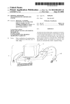
As shown in FIG. 3, the flash memory circuits receive a plurality of
input address signals A0-A16, data signals D00-D07 and control
signals consisting of chip enable, write enable, output enable, power
down and erase/program power supply signals CE, WE, OE, PWD,
and VPP respectively. The functions performed by these signals are
described in Appendix I. Ex. 1003, at 7:39-45.
OE
OUTPUT ENABLE: Gates the device’s outputs through the
data buffers during a read cycle.
OE is active low.
WE WRITE ENABLE: Controls writes to the command register and
array blocks. WE is active low. Addresses and data are latched
on the rising edge of the WE pulse.
Vpp ERASE/PROGRAM POWER SUPPLY
for erasing blocks of the array or programming bytes of each
block. Note: With Vpp < VPPI Max, memory contents cannot
be altered. When Vpp is at a high level, programming can take
place; if Vpp is at a low level, the memory array 54 functions as
a read only memory. Ex. 1003, at 15:25-37.
Ex. 1005, at ¶ 32.
Holtey I describes using, as an example, the same flash memory as Holtey
II, Intel’s 28F001BX 1M. Since both Holtey II and I use the same flash memory,
the teachings of Holtey I are applicable to and are necessarily present in Holtey II.
22


![SS400G MLSS Converter [Style:S2.2]](http://vs1.manualzilla.com/store/data/005726371_1-b873ef07ceb169a0226d293b313a67fd-150x150.png)