1
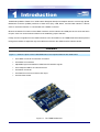
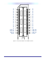
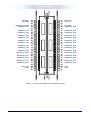
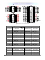
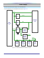
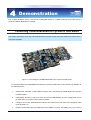
Terasic THDB-SUM
THDBHDB-SUM
Terasic HSMC to Santa Cruz Daughter Board
User Manual
Document Version 1.3
JULY. 29, 2009 by Terasic
Introduction
Page Index
INTRODUCTION................................................................................................................................................................................. 1
1.1
FEATURES ........................................................................................................................................................................... 1
1.2
GETTING HELP .................................................................................................................................................................... 2
ARCHITECTURE ................................................................................................................................................................................ 3
2.1
LAYOUT AND COMPONETS .................................................................................................................................................. 3
2.2
BLOCK DIAGRAM................................................................................................................................................................. 5
BOARD COMPONENTS ................................................................................................................................................................... 6
3.1
THE HSMC CONNECTOR ................................................................................................................................................... 6
3.2
SANTA CRUZ CONNECTOR ............................................................................................................................................... 10
3.3
USB ON-THE-GO TRANSCEIVER ..................................................................................................................................... 14
3.4
MICTOR CONNECTOR ....................................................................................................................................................... 16
3.5
SD CARD INTERFACE ....................................................................................................................................................... 18
3.6
SMA CONNECTOR ............................................................................................................................................................ 19
3.7
I2C SERIAL EEPROM ..................................................................................................................................................... 20
3.8
POWER SUPPLY ................................................................................................................................................................ 21
DEMONSTRATION .......................................................................................................................................................................... 22
4.1
CONNECTING THDB-SUM BOARD TO CYCLONE III START BOARD ............................................................................... 22
APPENDIX ......................................................................................................................................................................................... 24
5.1
REVISION HISTORY ........................................................................................................................................................... 24
5.2
ALWAYS VISIT THDB-SUM W EBPAGE FOR NEW MAIN BOARD ...................................................................................... 24
ii
Introduction
1
Introduction
THDB-SUM (HSMC to Santa Cruz / USB / Mictor Daughter Board) is an adapter board to convert High Speed
Mezzanine Connector (HSMC) interface to Santa Cruz (SC), USB, Mictor, and SD Card interface. It allows
users to use these interface on a host board with a HSMC connector.
Because of limited I/O numbers of the HSMC interface, the SC interface and USB port have to share the same
I/O pins. Users can choose which interface to be enabled by jumper selection.
Finally, the source signals from the HSMC interface to the SC header on the THDB-SUM board will be passed
through level shifters to adjust the logic level difference between the HSMC and SC interface board.
1.1 Features
Figure 1.1 shows the photo of the THDB-SUM board. The important features are listed below:
•
One HSMC connector for interface conversion
•
One Santa Cruz interface
•
Adjustable logic levels between HSMC and SC interface signals
•
One Hi-Speed USB On-The-Go transceiver
•
One Mictor Connector
•
One SMA Connector for external clock input
•
One SD Card Socket
Figure 1.1. The THDB-SUM board
1
Introduction
1.2 Getting Help
Here are some places to get help if you encounter any problem:
Email to [email protected]
Taiwan & China: +886-3-550-8800
Korea : +82-2-512-7661
Japan: +81-428-77-7000
2
Architecture
2
Architecture
This chapter describes the architecture of the THDB-SUM board including its PCB and block diagram.
2.1 Layout and Componets
The picture of the TDRB-SUM board is shown in Figure 2.1 and Figure 2.2. It depicts the layout of the board
and indicates the location of the connectors and key components.
HSMC Logical Level
Configuration Header (JP3)
Mini USB AB type
receptacle connector (J8)
USB Host/Peripheral Mode
Configuration Header(JP2)
JTAG TDI/TDO
Loopback Header (JP0)
USB On-The-Go transceiver (U11)
Santa Cruz Connector (J3)
EEPROM(U10)
Bus Switch (U1~U2)
SMA Connector (J6)
Level Shifters (U7~U8)
Santa Cruz Connector (J5)
Level Shifters (U3~U6)
Mictor Connector (J2)
Santa Cruz Connector (J4)
USB/SC Function Select
Header (JP1)
SC Connector Logical Level
Configuration Header (JP3)
Figure 2.1. The THDB-SUM PCB and component diagram
3
Architecture
HSMC Connector (J1)
SD Card Socket (J7)
Figure 2.2. The THDB-SUM Back side – HSMC connector view
The following components are provided on the THDB-SUM board :
•
HSMC expansion connector (J1)
•
Santa Cruz Headers(J3,J4,J5)
•
Mictor connector (J2)
•
SMA connector (J6)
•
Hi-Speed USB On-The-Go transceiver (U11)
o
Fully compliant with Universal Serial Bus Specification Rev. 2.0
o
Supplement to the USB 2.0 Specification Rev. 1.3
o
Supplement UTMI+ Low Pin Interface (ULPI) Specification Rev. 1.1
•
Mini USB AB type receptacle connector(J8)
•
Logic level configuration headers (JP3,JP4)
•
SD Card socket(J7)
•
I2C serial EEPROM (U10)
•
Level translator (U3~U9)
•
Bus Switches (U1~U2)
4
Architecture
2.2 Block Diagram
Figure 2.3 shows the block diagram of the THDB-SUM board
THDB-SUM
HSMC
Connector
Level
Shift
Bus
Switch
To
HSMC Interface
Host Board
SD Card Interface
SC Interface
USB Interface
Level
Shift
Santa Cruz
Connector
USB
Transceiver
SD Card
Socket
Mictor Connector Interface
Mictor
Connector
External Clock Input
SMA
Connector
I2C Interface
I2C Serial
EEPROM
Figure 2.3. The block diagram of the THDB-SUM board
5
Board Components
3
Board Components
This section will describe the detailed information of the components, connector interfaces, and the pin
mapping tables of the THDB-SUM board
3.1 The HSMC Connector
This section describes the HSMC connector on the THDB-SUM board
THDB-SUM board contains an Altera standard HSMC connector. All the other connector interfaces on the
THDB-SUM board are connected to the HSMC connector. Figure 3.1, Figure 3.2, and Figure 3.3 show the
pin-outs of the HSMC connector. Also, the JTAG interface of the HSMC connector is shown in the Figure 3.4. If
users don’t need to use the JTAG interface on the THDB-SUM board, please short the header JP0 to loopback
the TDI and TDO signals on the HSMC connector.
6
Board Components
NC
NC
2
4
1
3
NC
NC
NC
NC
6
8
5
NC
7
NC
NC
NC
10
12
9
11
NC
NC
NC
NC
14
16
13
NC
15
NC
NC
18
NC
20
17
19
NC
NC
NC
NC
22
24
21
NC
23
NC
NC
26
NC
28
25
27
NC
NC
NC
NC
30
32
29
31
NC
NC
HSMC_SCL
34
HSMC_TMS
36
33
35
HSMC_SDA
HSMC_TCK
HSMC_TDI
SD Wpn
38
40
37
39
HSMC_TDO
SD DAT1
Figure 3.1. The pin-outs of Bank 1 on the HSMC connector
7
Board Components
SD DAT3
SD DAT2
42
44
46
HSPROTO_RESET
48
HSPROTO_IO0
50
52
HSPROTO_IO1
54
HSPROTO_IO2
56
58
HSPROTO_IO3
60
HSPROTO_IO4
62
64
HSPROTO_IO5
66
HSPROTO_IO6
68
70
HSPROTO_IO7
72
HSPROTO_IO8
74
76
HSPROTO_IO9
78
HSPROTO_IO10
80
82
HSPROTO_IO11
84
HSPROTO_IO12
86
88
HSPROTO_IO13
90
HSPROTO_IO14
92
94
EXT_CLK
96
CLK2
98
100
41
43
45
47
49
51
53
55
57
59
61
63
65
67
69
71
73
75
77
79
81
83
85
87
89
91
93
95
97
99
SD_DAT0
SD_CLK
SD_CMD
HSPROTO_IO40
HSPROTO_IO29
HSPROTO_IO30
HSPROTO_IO31
HSPROTO_IO33
HSPROTO_IO32
HSPROTO_IO35
HSPROTO_IO34
HSPROTO_IO37
HSPROTO_IO36
HSPROTO_IO39
HSPROTO_IO38
HSPROTO_IO15
HSPROTO_IO16
HSPROTO_IO17
OSC
CLK1
Figure 3.2. The pin-outs of Bank 2 of the HSMC connector.
8
Board Components
MICTOR_D14
MICTOR_D15
12V
MICTOR_D16
MICTOR_D17
12V
MICTOR_D18
MICTOR_D19
12V
MICTOR_D20
MICTOR_D21
12V
MICTOR_D22
MICTOR_D23
12V
MICTOR_D24
HSPROTO_IO23
12V
HSPROTO_IO24
HSPROTO_IO25
12V
HSPROTO_IO26
HSPROTO_IO27
12V
HSPROTO_CARDSEL
HSPROTO_IO28
12V
MICTOR_CLK
DEV_SEL_R5
0
GND
102
104
106
108
110
112
114
116
118
120
122
124
126
128
130
132
134
136
138
140
142
144
146
148
150
152
154
156
158
160
101
103
105
107
109
111
113
115
117
119
121
123
125
127
129
131
133
135
137
139
141
143
145
147
149
151
153
155
157
159
MICTOR_D0
MICTOR_D1
V C C 33
MICTOR_D4
MICTOR_D5
V C C 33
MICTOR_D2
MICTOR_D3
V C C 33
MICTOR_D6
MICTOR_D13
V C C 33
MICTOR_D12
MICTOR_D11
V C C 33
MICTOR_D10
MICTOR_D9
V C C 33
MICTOR_D8
MICTOR_D7
V C C 33
HSPROTO_IO18
HSPROTO_IO19
V C C 33
HSPROTO_IO20
HSPROTO_IO21
V C C 33
HSPROTO_IO22
TR_CLK
V C C 33
Figure 3.3. The pin-outs of Bank 3 of the HSMC connector
HSMC_TDI
R1
0
MICTOR_TDI
HSMC_TDO
R2
0
MICTOR_TDO
R3
0 NM
R4
0 NM
HSMC_TDI
1
2
NM:No Mount
HSMC_TDI
JP0
Open : JTAG Chain
Close : JTAG Pass
Figure 3.4. The JTAG interface setting of the HSMC connector.
9
Board Components
3.2 Santa Cruz Connector
This section describes the Santa Cruz connector on the THDB-SUM board
The THDB-SUM board comes with Santa Cruz connectors (J3, J4 and J5) to connect to a daughter board with
Santa Cruz interface. On the THDB-SUM, the pin of SC connector not directly connects with HSMC connector.
Owing to the limitation of number of HSMC connector I/O pins, SC connector and USB transceiver share some
I/O pins together, Please refer to Figure 3.5, those I/O pass through a Bus Switch chip first and then connect with
HSMC connector. Therefore users can only choose one function between SC connector and USB transceiver.
Users can refer to Table3.1 and use JP2 to choose a function
In addition, from the Figure 3.6, there are several level shift chips between HSMC and SC. Theses level shift
chips convert the logic levels of the signals between the HSMC and Santa Cruz connectors according to the
configurations of the headers (JP3, JP4). With this feature, users can use different I/O standards between the
HSMC host board and SC interface daughter board. Table 3.2 and Table 3.3 list the configurations of the voltage
level of the HSPROTO_IO BUS and the PROTO_IO BUS, respectively.
HSMC Connector (J1)
HSPROTO_CARDSEL
HSPROTO_IO[40..15]
Level
Shifters
(U3~U8)
27
PROTO_RESET
PROTO_CARDSEL
PROTO_IO[40..0]
43
Santa Cruz
Connectors
(J3~J5)
SWPROTO_RESET
SWPROTO_IO[14..0]
HSPROTO_RESET
HSPROTO_IO[14..0]
16
16
BUS
Switches
(U1~U2)
USB_D[7..0]
USB_CS_n
USB_CLKOUT
14
DEV_SEL
JP1
Open : USB
Close : Santa Cruz
USB_STP
USB_DIR
USB_NXT
USB_RESET_n
USB OTG
Transceiver
(U11)
Figure 3.5. The I/O distribution of the HSMC, Santa Cruz, and USB transceiver interface.
Table 3.1 The configuration of the Enable function on bus switch chip
JP1 setting
Enable Function
Open
USB OTC Transceiver
Close
Santa Cruz conenctor
10
Board Components
Open : 3.3V
Close : 5V
Open : 2.5V
Close : 3.3V
JP3
JP4
HSMC Connector (J1)
VCCA
HSPROTO_RESET
HSPROTO_CARDSEL
HSPROTO_IO[40..0]
VCCB
Level
Shifters
(U3~U8)
PROTO_RESET
PROTO_CARDSEL
PROTO_IO[40..0]
43
43
Santa Cruz
Connectors
(J3~J5)
Figure 3.6 The diagram of the logic level transform block
Table 3.2 The configuration of the logic level on the HSPROTO_IO
BUS
JP3 setting
Logic level of the HSPROTO_IO BUS
Open
2.5V
Close
3.3V
Table 3.3 The configuration of the logic level on the PROTO_IO BUS
JP4 setting
Logic level of the PROTO_IO BUS
Open
3.3V
Close
5V
Finally, Figure 3.5 shows the pin-outs of the Santa Cruz connector. Detailed pin mappings between J3, J4, and
J5 to the HSMC connector is listed in Table 3.4, Table 3.5, and Table 3.6, respectively.
Note:
Because of the characteristic of the level translators, the data rate of the HSPROTO_IO and PROTO_IO
bus should be under 100 Mbps.
11
Board Components
Figure 3.7 Santa Cruz connector pin-outs
Table 3.4 The pin assignments of the Santa Cruz connector J3
HSMC Pin
SC Pin Number
SC Signal Name
HSMC Signal Name
HSMC Pin Name
Number
3
PROTO_IO40
49
HSPROTO_IO40
HSMC_TX_N0
4
PROTO_IO29
53
HSPROTO_IO29
HSMC_TX_P1
5
PROTO_IO30
55
HSPROTO_IO30
HSMC_TX_N1
6
PROTO_IO31
59
HSPROTO_IO31
HSMC_TX_P2
7
PROTO_IO32
65
HSPROTO_IO32
HSMC_TX_P3
8
PROTO_IO33
61
HSPROTO_IO33
HSMC_TX_N2
9
PROTO_IO34
71
HSPROTO_IO34
HSMC_TX_P4
10
PROTO_IO35
67
HSPROTO_IO35
HSMC_TX_N3
11
PROTO_IO36
77
HSPROTO_IO36
HSMC_TX_P5
12
PROTO_IO37
73
HSPROTO_IO37
HSMC_TX_N4
13
PROTO_IO38
83
HSPROTO_IO38
HSMC_TX_P6
14
PROTO_IO39
79
HSPROTO_IO39
HSMC_TX_N5
Table 3.5 The pin assignments of the Santa Cruz connector J4
HSMC Pin
SC Pin Number
SC Signal Name
HSMC Signal Name
HSMC Pin Name
Number
9
OSC
95
OSC
HSMC_CLKOUT_P1
11
CLK1
97
CLK1
HSMC_CLKOUT_N1
13
CLK2
98
CLK2
HSMC_CLKIN_N1
12
Board Components
Table 3.6 The pin assignments of the Santa Cruz connector J5
HSMC Pin
SC Pin Number
SC Signal Name
HSMC Signal Name
HSMC Pin Name
Number
1
PROTO_RESET
48
HSPROTO_RESET
HSMC_RX_P0
3
PROTO_IO0
50
HSPROTO_IO0
HSMC_RX_N0
4
PROTO_IO1
54
HSPROTO_IO1
HSMC_RX_P1
5
PROTO_IO2
56
HSPROTO_IO2
HSMC_RX_N1
6
PROTO_IO3
60
HSPROTO_IO3
HSMC_RX_P2
7
PROTO_IO4
62
HSPROTO_IO4
HSMC_RX_N2
8
PROTO_IO5
66
HSPROTO_IO5
HSMC_RX_P3
9
PROTO_IO6
68
HSPROTO_IO6
HSMC_RX_N3
10
PROTO_IO7
72
HSPROTO_IO7
HSMC_RX_P4
11
PROTO_IO8
74
HSPROTO_IO8
HSMC_RX_N4
12
PROTO_IO9
78
HSPROTO_IO9
HSMC_RX_P5
13
PROTO_IO10
80
HSPROTO_IO10
HSMC_RX_N5
14
PROTO_IO11
84
HSPROTO_IO11
HSMC_RX_P6
15
PROTO_IO12
86
HSPROTO_IO12
HSMC_RX_N6
16
PROTO_IO13
90
HSPROTO_IO13
HSMC_RX_P7
17
PROTO_IO14
92
HSPROTO_IO14
HSMC_RX_N7
18
PROTO_IO15
85
HSPROTO_IO15
HSMC_TX_N6
21
PROTO_IO16
89
HSPROTO_IO16
HSMC_TX_P7
23
PROTO_IO17
91
HSPROTO_IO17
HSMC_TX_N7
25
PROTO_IO18
143
HSPROTO_IO18
HSMC_TX_P15
27
PROTO_IO19
145
HSPROTO_IO19
HSMC_TX_N15
28
PROTO_IO20
149
HSPROTO_IO20
HSMC_TX_P16
29
PROTO_IO21
151
HSPROTO_IO21
HSMC_TX_N16
31
PROTO_IO22
155
HSPROTO_IO22
HSMC_CLKOUT_P2
32
PROTO_IO23
134
HSPROTO_IO23
HSMC_RX_N13
33
PROTO_IO24
138
HSPROTO_IO24
HSMC_RX_P14
35
PROTO_IO25
140
HSPROTO_IO25
HSMC_RX_N14
36
PROTO_IO26
144
HSPROTO_IO26
HSMC_RX_P15
37
PROTO_IO27
146
HSPROTO_IO27
HSMC_RX_N15
38
PROTO_CARDSEL
150
HSPROTO_CARDSEL
HSMC_RX_P16
39
PROTO_IO28
152
HSPROTO_IO28
HSMC_RX_N16
13
Board Components
3.3 USB On-The-Go transceiver
This section describes the USB On-The-Go transceiver on the THDB-SUM board
The THDB-SUM is equipped with a NXP ISP1504C USB On-The-Go transceiver (U11) and Mini USB AB type
receptacle connector (J8) to provide USB interface to the HSMC interface host board. The ISP1504 is a
Universal Serial Bus (USB) On-The-Go (OTG) transceiver that is fully compliant with Universal Serial Bus
Specification Rev. 2.0, On-The-Go Supplement to the USB 2.0 Specification Rev. 1.3 and UTMI+ Low Pin
Interface (ULPI) Specification Rev. 1.1.
The pervious section, Santa Cruz Connector, has mentioned that USB transceiver and Santa Cruz connector
share the I/Os which connect to HSMC connector, which means users can only choose one function between
USB and Satan Cruz interface, If users would like to choose the function of USB transceiver, please turn on
JP2. For more detailed information about this transceiver, please refer to the datasheet which can be found in
the NXP’s website.
In addition, for OTG implementations, a 2-pin header named JP1 is connected with ID (identification) pin of
the USB OTG transceiver and micro-USB receptacle. As shown in Figure 3.8, The logic level of the ID pin on
the USB OTG transceiver can be configured to logic high or low via JP1. As defined in On-The-Go supplement
to the USB 2.0 specification Rev. 1.3, the ID pin dictates the initial role of the link. If ID is detected as HIGH,
the link must assume the role of a peripheral. If ID is detected as LOW, the link must assume a
host role. Table 3.7 shows the JP1 configuration setting for the ID.
Finally, the detailed pin mappings between the USB On-The-Go transceiver and the HSMC connector are
shown in Table3.8.
Table 3.7 The configuration of the ID pin
JP2 setting
Host or peripheral role
Open
Peripheral
Close
Host
14
Board Components
HSMC Connector
(J1)
Jack-Mini- USB-AB
(J8)
USB
USB _D[7..0]
USB_RESET_n
HSPROTO_IO
VBUS
DM
DP
ID
DATA[7..0]
USB_CS_n
CS
RESET
Bus
Switch
(U1,U2)
NXP
ISP1504C
(U11)
USB_DIR
USB_STP
USB_NXT
USB_CLKOUT
JP2 Close = Host
Open = Peripheral
DIR
STP
NXT
CLOCK
X1
XTAL1
XTAL2
XTAL1
XTAL2
26MHZ
JP1 Open
Figure 3.8 The block diagram of the USB OTG transceiver and HSMC connector
Table 3.8 The pin assignments of the USB OTG Transceiver U11
USB Pin
HSMC Pin
USB Signal Name
Number
HSMC Pin
HSMC Signal Name
Number
Name
1
USB_D0
48
HSPROTO_RESET
HSMC_RX_P0
17
USB_RESET_n
86
HSPROTO_IO12
HSMC_RX_N6
19
USB_DIR
84
HSPROTO_IO11
HSMC_RX_P6
20
USB_STP
80
HSPROTO_IO10
HSMC_RX_N5
21
USB_NXT
78
HSPROTO_IO9
HSMC_RX_P5
23
USB_D7
74
HSPROTO_IO8
HSMC_RX_N4
24
USB_D6
72
HSPROTO_IO7
HSMC_RX_P4
25
USB_D5
68
HSPROTO_IO6
HSMC_RX_N3
26
USB_D4
66
HSPROTO_IO5
HSMC_RX_P3
27
USB_CLKOUT
62
HSPROTO_IO4
HSMC_RX_N2
28
USB_D3
60
HSPROTO_IO3
HSMC_RX_P2
29
USB_CS_n
56
HSPROTO_IO2
HSMC_RX_N1
31
USB_D2
54
HSPROTO_IO1
HSMC_RX_P1
32
USB_D1
50
HSPROTO_IO0
HSMC_RX_N0
15
Board Components
3.4 Mictor Connector
This section describes how to use the Mictor connector on the THDB-SUM board
The Mictor connector (J2) can be used for logic analysis on the HSMC-interfaced host board by connecting an
external scope or a logic analyzer to it. Figure 3.9 shows the pin-outs of the Mictor connector. Table 3.9 shows
the detailed pin mappings between the Mictor connector and the HSMC connector.
Figure 3.9 Mictor connector pin-outs
Table 3.9 The pin assignments of the Mictor connector J2
Mictor
Mictor Connector
HSMC Pin
Signal Name
Number
5
MICTOR_CLK
6
Connector
HSMC Signal Name
HSMC Pin Name
156
MICTOR_CLK
HSMC_CLKIN_P2
TR_CLK
157
TR_CLK
HSMC_CLKOUT_N2
7
MICTOR_D24
132
MICTOR_D24
HSMC_RX_P13
8
MICTOR_D13
121
MICTOR_D13
HSMC_TX_N11
9
MICTOR_D23
128
MICTOR_D23
HSMC_RX_N12
10
MICTOR_D12
125
MICTOR_D12
HSMC_TX_P12
13
MICTOR_D22
126
MICTOR_D22
HSMC_RX_P12
16
MICTOR_D11
127
MICTOR_D11
HSMC_TX_N12
18
MICTOR_D10
131
MICTOR_D10
HSMC_TX_P13
20
MICTOR_D9
133
MICTOR_D9
HSMC_TX_N13
22
MICTOR_D8
137
MICTOR_D8
HSMC_TX_P14
23
MICTOR_D21
122
MICTOR_D21
HSMC_RX_N11
Pin Number
16
Board Components
24
MICTOR_D7
139
MICTOR_D7
HSMC_TX_N14
25
MICTOR_D20
120
MICTOR_D20
HSMC_RX_P11
26
MICTOR_D6
119
MICTOR_D6
HSMC_TX_P11
27
MICTOR_D19
116
MICTOR_D19
HSMC_RX_N10
28
MICTOR_D5
109
MICTOR_D5
HSMC_TX_N9
29
MICTOR_D18
114
MICTOR_D18
HSMC_RX_P10
30
MICTOR_D4
107
MICTOR_D4
HSMC_TX_P9
31
MICTOR_D17
110
MICTOR_D17
HSMC_RX_N9
32
MICTOR_D3
115
MICTOR_D3
HSMC_TX_N10
33
MICTOR_D16
108
MICTOR_D16
HSMC_RX_P9
34
MICTOR_D2
113
MICTOR_D2
HSMC_TX_P10
35
MICTOR_D15
104
MICTOR_D15
HSMC_RX_N8
36
MICTOR_D1
103
MICTOR_D1
HSMC_TX_N8
37
MICTOR_D14
102
MICTOR_D14
HSMC_RX_P8
38
MICTOR_D0
101
MICTOR_D0
HSMC_TX_P8
11
MICTOR_TDO
37
HSMC_TDO
HSMC_TDO
15
MICTOR_TCK
35
HSMC_TCK
HSMC_TCK
17
MICTOR_TMS
36
HSMC_TMS
HSMC_TMS
19
MICTOR_TDI
38
HSMC_TDI
HSMC_TDI
To use this interface, user needs to configure the JTAG interface on the HSMC interface host board. For
example, the steps of controlling the Cyclone III start board using Mictor interface is shown below:
1. Connecting the THDB-SUM board to the Cyclone III Start Board.
2. Removing the jumpers of JP1 and JP2 of the Cyclone III Start Board to connect the JTAG interface
between Cyclone III FPGA and the THDB-SUM board.
3. Short the TDI and TDO pins of the JTAG connector(J4), as shown in Figure 3.10
4. Disable the built-in USB blaster by shorting JP8 on the Cyclone III Starter Board
The above FOUR steps will make a closed JTAG chain as shown in Figure 3.11
17
Board Components
Open JP1 nad JP2
Short TDI and TDO
pin of the J4
J4
Short
Close JP8
With jumper
Figure 3.10 The configuration of the Cyclone III start board for controlling the JTAG chain using the Mictor
connector
THDB-SUM Board
Cyclone III Start Board
USB3V
CLOSE
JP8
VCC25
OPEN
Mictor connector
J2
JP1
OPEN
TDI
TDI
TDO
TDO
J4
MICOTR_TDI
MICOTR_TDI
MICOTR_TDO
JP2
MICOTR_TDO
HSMC_TDI
HSMC_TDI
JTAG_TDO
LF_TDI
HSMC_TDO
HSMC_TDO
Cyclone III
TDO
LF_TDO
HSMC
SHORT
LF_TDO
TDI
ADG3304
MAX 3128
Built-in
Blaster
TDI
TDO
CII_TDO
ADG3308
Figure 3.11 The JTAG chain between the THDB-SUM board and Cyclone III Start Board
3.5 SD Card Interface
This section describes the SD Card Interface on the THDB-SUM board
The THDB-SUM has a SD card socket and can be accessed as optional external memory in both SPI and
1-bit SD mode. Table X shows the pinout of the SD card socket with HSMC connector. Figure 3.12 and Table
3.10 shows the pin connection and pin-out between the Mictor connector and HSMC connector, respectively.
18
Board Components
HSMC Connector
SD Card Socket
SD_DAT2
LF_DAT2
9
DAT2
SD_DAT3
SD_CMD
SD_CLK
SD_DAT0
SD_DAT1
SD_WPn
LF_DAT3
LF_CMD
LF_CLK
LF_DAT0
LF_DAT1
LF_WPn
1
2
DAT3
CMD
CLK
DAT0
DAT1
WPn
Level
Shift
(U9)
5
7
8
11
Figure 3.12 The block diagram of the SD Card socket and HSMC connector
Table 3.10 The pin assignments of the SD Card Socket J7
SD Card Socket
SD Card Socket
HSMC Pin
Pin Number
Signal Name
Number
1
LF_DAT3
2
HSMC Signal Name
HSMC Pin Name
42
SD_DAT3
HSMC_D1
LF_CMD
47
SD_CMD
HSMC_TX_P0
5
LF_CLK
43
SD_CLK
HSMC_D2
7
LF_DAT0
41
SD_DAT0
HSMC_D0
8
LF_DAT1
39
SD_DAT1
HSMC_CLKOUT0
9
LF_DAT2
44
SD_DAT2
HSMC_D3
11
LF_WPn
40
SD_WP_N
HSMC_CLKIN0
3.6 SMA Connector
This section describes the SMA connector on the THDB-SUM board
The THDB-SUM board provides a SMA connector (J6) for external clock input. The pin assignments of the
SMA connector are shown in Table 3.11.
Table 3.11 The pin assignments of the SMA Connector J6
SD Card Socket
SD Card Socket
HSMC Pin
Pin Number
Signal Name
Number
1
EXT_CLK
96
19
HSMC Signal Name
HSMC Pin Name
EXT_CLK
HSMC_CLKIN_P1
Board Components
3.7 I2C Serial EEPROM
This section describes the I2C Serial EEPROM on the THDB-SUM board
The THDB-SUM board provides an EEPROM (U10) which can be configured by the I2C interface. The size of
the EEPROM is 128 bit that can store the board information or user’s data. The detailed pin description
between EEPROM and HSMC connector is listed in the Table 3.12.
HSMC Connector
R31
HSMC_SCL
HSMC_SDA
VCC33
A0
R32
SCL
SDA
EEPROM
(U10)
R33
VCC33
A1
R34
R35
A2
VCC33
R36
Default Address : 0x0
Table 3.13 The block diagram of the EEPROM and HSMC connector
Table 3.12 The pin assignments of the EEPROM U10
EEPROM Pin
EEPROM Signal
HSMC Pin
Number
Name
Number
5
HSMC_SDA
33
HSMC_SDA
6
HSMC_SCL
34
HSMC_SCL
HSMC Signal Name
20
Board Components
3.8 Power Supply
This section describes the power supply on the THDB-SUM board
The power distribution on the THDB-SUM board is shown in Figure 3.14.
12V
VCC50
REG3
REG2
HSMC
Connector
(J1)
Santa Cruz
Connector
(J3~J5)
VSC
JP4
VHSMC
VCCA VCCB
Level
Shifters
(U3~U8)
VCC33
REG1
JP3
VCCA VCCB
Level
Shifters
(U9)
EEPROM
(U10)
Mictor
Connector
(J2)
VCC33
VCC50
SD Card
Socket
(J7)
Figure 3.14. THDB-SUM board power distribution diagram.
21
USB
(U11)
Demonstration
4
Demonstration
This chapter illustrates how to connect the THDB-SUM board to a HSMC interface host board using a
Cyclone III Starter Board as an example
4.1 Connecting THDB-SUM Board to Cyclone III Start Board
This section describes how to use THD-SUM board the Cyclone III start board and what users need to know
during the operation
Figure 4.1 Connecting the THDB-SUM board to the Cyclone III start board
To correctly operate the THDB-SUM board with the Cyclone III start board, users need to pay attention to
the following notes:
1.
Observe the orientation of the HSMC connector when connecting the THDB-SUM to the Cyclone
III Starter Board.
2.
Users MUST short Pin 1 and Pin 2 of the JP3 on the THDB-SUM to force the voltage level to 2.5V
to match the 2.5V IO pins of the Cyclone III board.
3.
Configure JP4 of the THDB-SUM according to the logic level of the Santa Cruz daughter board
(refer to Table 3.2)
4.
Please note that there are two LVDS pairs on the HSMC connector: the HSMC_CLK_p1/n1 (form a
22
Demonstration
close loop via R3) and HSMC_CLKIN_p2/n2 (form a close loop via R4). Therefore, using any one
of the signal in a LVDS pair under single-ended mode will prevent users from using the other signal
in the same pair.
23
Appendix
5
Appendix
5.1 Revision History
Date
Change Log
SEP 3, 2008
Initial Version
MAR 13,2009
Modify Figure 3.3
DEC 2, 2009
Corrections for tables 3.1 & 3.7. Modify Ch.4 section
5.2 Always Visit THDB-SUM Webpage for New Main board
We will be continuing providing interesting examples and labs on our THDB-SUM
webpage. Please visit www.altera.com or SUM.terasic.com for more information.
24