1
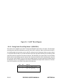
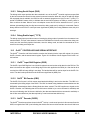
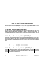
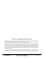
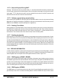
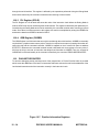
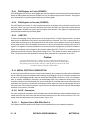
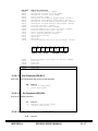
SECTION 10 ON-CHIP EMULATOR 10.1 INTRODUCTION Conventional methods of system development (for example the DSP56001) consist of a program which resides in the DSP program memory (monitor). An interface circuit which either uses on-chip resources or an additional program memory address communicates with a host computer or terminal. This technique is not transparent, loads the DSP bus and sometimes interferes with the user system configuration. To emulate the DSP in a user’s target system an expensive cable must be used to bring out the DSP pins onto the system under development. The DSP96002’s on-chip emulation (OnCE) circuitry provides a means of interacting with the DSP96002 and its peripherals non-intrusively so that a user may examine registers, memory or on-chip peripherals. This will facilitate hardware/software development on the DSP96002 processor. To achieve this, special circuits and dedicated pins on the DSP96002 die are defined to avoid sacrificing any user accessible on-chip resource. A key feature of the OnCE dedicated pins is to allow the user to insert the DSP96002 into his target system yet retaining debug control. The need for a costly cable which brings out the DSP96002 footprint on an emulator system is eliminated because of the easy access to the dedicated OnCE debug serial port. Figure 10-1illustrates the block diagram of the OnCE serial interface. 10.2 ON-CHIP EMULATION (OnCE ) PINOUT 10.2.1 Debug Serial Input/Chip Status 0 (DSI/OS0) Serial data or commands are provided to the OnCE controller through the DSI/OS0 pin when it is an input. The data received on the DSI pin will be recognized only when the DSP96002 has entered the debug mode of operation. Data must have valid TTL logic levels before being latched on the falling edge of the serial clock. Data is always shifted into the OnCE serial port most significant bit (MSB) first. When an output, this pin in conjunction with the OS1 pin, provides information about the chip status indicating why the debug mode cannot be entered in response to an external request. The DSI/OS0 pin is an output when not in Debug Mode (until the acknowledge signal is issued to the Command Controller). When switching from output to input, the pin is three-stated. In order to avoid any possible glitches, an external pull-down resistor should be attached to this pin. During hardware reset, this pin is defined as an output and it is driven low. OnCE is a trademark of Motorola Inc. MOTOROLA DSP96002 USER’S MANUAL 10 - 1 Figure 10-1. OnCE Block Diagram 10.2.2 Debug Serial Clock/Chip Status 1 (DSCK/OS1) The serial clock is supplied to the OnCE through the DSCK/OS1 pin when it is an input. The serial clock provides pulses required to shift data into and out of the OnCE serial port. Data is clocked into the OnCE on the falling edge and is clocked out of the OnCE serial port on the rising edge. When an output, this pin in conjunction with the OS0 pin, provides information about the chip status describing why the debug mode cannot be entered in response to an external request. The DSCK/OS1 pin is output when not in the Debug Mode (until the acknowledge signal is issued to the Command Controller). When switching from output to input, the pin is three-stated. In order to avoid any possible glitches, an external pull-down resistor should be attached to this pin. During hardware reset, this pin is defined as an output and it is driven low. The maximum SCK frequency is one third of the system clock frequency. OS1 0 0 1 1 10 - 2 OS0 0 1 0 1 Status Normal state STOP or WAIT state Core busy state Core or DMA busy state DSP96002 USER’S MANUAL MOTOROLA 10.2.3 Debug Serial Output (DSO) The debug serial output provides the data contained in one of the OnCE controller registers as specified by the last command received from the external command controller. When idle, this pin is held high. When the requested data is available, the DSO line will be asserted (negative true logic) for two T cycles (2T = period of DSP96002 master clock) to indicate that the serial shift registers are ready to receive clocks in order to deliver the data. When a trace or breakpoint occurs this line will be asserted for one T cycle to indicate (acknowledge) that the chip has entered the debug mode and is waiting for commands. Data is always shifted out the OnCE serial port most significant bit (MSB) first. During hardware reset, this pin is held high. — – 10.2.4 Debug Enable Input ( D R) The debug request input provides a means of entering the debug mode of operation from the external command controller. This pin, when asserted, causes the DSP96002 to finish the current instruction being executed, save the instruction pipeline information, enter the debug mode, and wait for commands to be entered from the debug serial input line. 10.3 OnCE CONTROLLER AND SERIAL INTERFACE The OnCE Controller and Serial Interface contains the following blocks: input shift register, bit counter, OnCE decoder, and the status/control register. Figure 10-2 illustrates a block diagram of the OnCE serial interface. 10.3.1 OnCE Input Shift Register (OISR) The OnCE Input Shift Register is an 8-bit shift register that receives the serial data from the DSI line. The data is clocked into the register on the falling edge of the clock applied to the DSCK pin. After the 8th bit is received, the OISR will stop shifting in new data. The latched data will be used as input for the OnCE Decoder. The data is always shifted into the OISR most significant bit (MSB) first. 10.3.2 OnCE Bit Counter (OBC) The OnCE Bit Counter is a 5-bit counter associated with shifting in and out the data bits. The OBC is incremented by the falling edges of the DSCK. The OBC is cleared during hardware reset and whenever the DSP96002 acknowledges that the Debug Mode has been entered. The OBC supplies two signals to the OnCE Decoder: one indicating that the first 8 bits were shifted-in (so a new command is available) and the second indicating that 32 bits were shifted-in (the data associated with that command is available) or that 32 bits were shifted-out (the data required by a read command was shifted out). 10.3.3 OnCE Decoder (ODEC) The OnCE Decoder supervises the entire OnCE activity. It receives as input the 8-bit command from the OISR, two signals from OBC (one indicating that 8 bits have been received and the other that 32 bits have MOTOROLA DSP96002 USER’S MANUAL 10 - 3 Figure 10-2. OnCE Controller and Serial Interface been received), and two signals indicating that the core was halted and the DMA was halted. The ODEC generates all the strobes required for reading and writing the selected OnCE registers. 10.3.4 OnCE Status and Control Register (OSCR) The Status and Control Register is a 32-bit register used to select the events that will put the chip in Debug Mode (see Figure 10-3). Breakpoints may be disabled or enabled on one or more memory spaces. The Trace Mode of operation is also selected from OSCR. The control bits are read/write while the status bits are read only. 10.3.4.1 Program Memory Breakpoint Enable (PBE0-PBE1) Bits 0-1 These control bits unmask program memory breakpoints allowing break-point interrupts to occur when a program memory address is within the low and high program memory address registers and will select whether the breakpoint will be recognized for read or write accesses. These bits are cleared on hardware reset. PBE1 0 0 1 1 PBE0 0 1 0 1 Selection Breakpoint Breakpoint Breakpoint Breakpoint disabled on write accesses on read accesses on both read and write accesses 10.3.4.2 Program Memory Breakpoint Selection (PBS0-PBS1) Bits 2-3 These control bits select whether the program memory breakpoints will be recognized on core program memory fetches, core program memory accesses (MOVEM or MOVEP) or DMA program memory accesses. These bits are cleared on hardware reset. 10 - 4 DSP96002 USER’S MANUAL MOTOROLA 31 19 18 * TO 17 DBO 16 15 PBO 9 * 8 TME 7 6 DBS1 DBS0 5 4 DBE1 DBE0 3 PBS1 2 1 0 PBS0 PBE1 PBE0 * Read as zeroes, should be written with zero for future compatibility. Figure 10-3. OnCE Programming Model PBS1 0 0 1 1 PBS0 0 1 0 1 Selection Breakpoint Breakpoint Breakpoint Breakpoint on on on on Core fetch accesses Core P move accesses Core and P move accesses DMA accesses When PBS1=0 and PBS0=0, program memory breakpoints are enabled only for fetches of the first instruction word of instructions that are actually executed (not the killed instructions and not the second word of jump instructions that are not taken). Program memory address breakpoints occur after the fetched instruction is executed and the breakpoint counter has been decremented to zero. When PBS1=0 and PBS0=1, program memory breakpoints are enabled only for explicit program memory access resulting from MOVEP and MOVEM instructions to/from P: memory space (MOVEP P:..,.. or MOVE ..,P:..). When PBS1=1 and PBS0=0, program memory breakpoints are enabled for any access to the Program space (any kind of PMOVE, true and false fetches, fetches of 2nd word, etc.). When PBS1=1 and PBS0=1, program memory breakpoints are enabled only for DMA accesses to program memory space. 10.3.4.3 Data Memory Breakpoint Enable (DBE0-DBE1) Bit 4-5 These control bits enable data memory breakpoints to occur when a data memory address is within the low and high data memory address registers and will select whether the breakpoint will be recognized for read or write accesses. These bits are cleared on hardware reset. DBE1 0 0 1 1 DBE0 0 1 0 1 Selection Breakpoint Breakpoint Breakpoint Breakpoint disabled on write accesses on read accesses on both read and write accesses 10.3.4.4 Data Memory Breakpoint Selection (DBS0-DBS1) Bits 6-7 These control bits select whether the data memory breakpoints will be recognized on core or DMA data memory accesses for X or Y data spaces. These bits are cleared on hardware reset. DBS1 0 0 1 1 MOTOROLA DBS0 0 1 0 1 Selection Breakpoint Breakpoint Breakpoint Breakpoint on on on on X Y X Y DSP96002 USER’S MANUAL Core Core DMA DMA fetch fetch fetch fetch addresses addresses addresses addresses 10 - 5 10.3.4.5 Trace Mode Enable (TME) Bit 8 This control bit, when set, enables the Trace Mode causing the chip to enter the Debug Mode whenever the execution of an instruction is completed and the Trace Counter is zero. This bit is cleared on hardware reset. 10.3.4.6 Reserved (Bits 9-15, 20-31) These bits are reserved for future use. They are read as zero and should be written as zero for future compatibility. 10.3.4.7 Program Memory Breakpoint Occurrence (PBO) Bit 16 This read only status bit is set when a program memory breakpoint occurs. It is used by the external command controller to determine how the Debug Mode was entered. This bit is cleared on hardware reset and when the OSCR is read. 10.3.4.8 Data Memory Breakpoint Occurrence (DBO) Bit 17 This read only status bit is set when a data memory breakpoint occurs. It is used by the external command controller to determine how the debug mode was entered. This bit is cleared on hardware reset and when the OSCR is read. 10.3.4.9 Trace Occurrence (TO) Bit 18 This read only status bit is set when the debug mode of operation is entered from a decrement to zero of the trace counter and the trace mode has been armed. This bit is cleared on hardware reset and when the OSCR is read. 10.3.4.10 Software Debug Occurrence (SWO) Bit 19 This status bit is set when the debug mode of operation is entered due to the execution of the (F)DEBUGcc instruction with condition true. This bit is cleared on hardware reset and when the OSCR is read. 10.4 OnCE HARDWARE BREAKPOINT LOGIC Hardware breakpoints may be set on program memory or data memory locations. Also, the breakpoint does not have to be in the program flow but within an approximate address range of where the program may be executing. This significantly increases the programmer’s ability to monitor what the program is doing realtime (see Section 10-3.4 for programming details). The breakpoint logic has two identical sections: one for program memory breakpoints and one for data memory breakpoints. Each section contains latches for core or DMA addresses, registers that store the upper and lower address limit, comparators and a counter. Figure 10-4 illustrates a block diagram of the OnCE Program Memory Breakpoint Logic and Figure 10-5 illustrates a block diagram of the OnCE Data Memory Breakpoint Logic. 10.4.1 Address Comparator Breakpoint Registers Address comparators are useful in determining where a program may be getting lost or when data is being written to areas that should not be written to in real-time. They are also useful in halting a program at a spe- 10 - 6 DSP96002 USER’S MANUAL MOTOROLA Figure 10-4. Program Memory Breakpoint Logic cific point to examine/change registers or memory. Using address comparators to set breakpoints enables the user to set breakpoints in RAM or ROM and while in any operating mode. The low address comparator will cause a logic true signal when the address on the bus is greater than or equal to the low boundary. The high address comparator will cause a logic true signal when the address on the bus is less than or equal to the high boundary. If the low address comparator and high address comparator both issue a logic true signal, the address is within the address range and the breakpoint counter is decremented if the contents are greater than zero. If zero, the counter is not decremented and the breakpoint exception occurs. Conditional jump addresses produced by the instruction pipeline that are within a program address block being monitored are only valid if the conditional jump instruction occurs, otherwise the conditional jump ad- MOTOROLA DSP96002 USER’S MANUAL 10 - 7 Figure 10-5. Data Memory Breakpoint Logic dress is ignored. Program memory address breakpoints occur after the opcode or operand is executed and the breakpoint counter has been decremented to zero. Data memory address breakpoints also occur after the execution of the instruction which formed the data memory address and the breakpoint counter has decremented to zero. All breakpoint registers are controlled by the debug status and control register, OSCR. 10.4.2 Breakpoint Counter The breakpoint counter is useful for stopping at the nth iteration of a program loop or when the nth occurrence of a data memory access occurs. This information significantly decreases algorithm debug time and 10 - 8 DSP96002 USER’S MANUAL MOTOROLA provides a means of checking hot spots in program segments as well as peripheral or data memory accesses. Program hot spots may be statistically evaluated by setting the breakpoint counter to a value, setting a program address in the program address comparator registers, passing control of the DSP96002 back to the user program and checking to see if a breakpoint occurs after n iterations of the program memory access. The breakpoint counter becomes a powerful tool when debugging real-time fast interrupt sequences such as servicing an A/D or D/A converter or stopping after a specific number of host transfers have occurred. The breakpoint counters are cleared by hardware reset. 10.4.3 Program Memory Address Latch (OPAL) The Program Memory Address Latch is a 32-bit register that latches the PAB on every cycle during the core slot or during the DMA slot according to the PBS1-PBS0 bits in OSCR. 10.4.4 Program Memory Upper Limit Register (OPULR) The Program Memory Upper Limit Register is a 32-bit register that stores the program memory breakpoint upper limit. OPULR can only be read or written through the serial interface. Before enabling breakpoints, OPULR must be loaded by the command controller. 10.4.5 Program Memory Lower Limit Register (OPLLR) The Program Memory Lower Limit Register is a 32-bit register that stores the program memory breakpoint lower limit. OPLLR can only be read or written through the serial interface. Before enabling breakpoints, OPLLR must be loaded by the command controller. 10.4.6 Program Memory High Address Comparator (OPHC) The Program Memory High Address Comparator compares the current program memory address (stored by OPAL) with the OPULR contents. If OPULR is higher or equal than OPAL then the comparator delivers a signal indicating that the address is lower than or equal to the high limit. 10.4.7 Program Memory Low Address Comparator (OPLC) The Program Memory Low Address Comparator compares the current program memory address (stored by OPAL) with the OPLLR contents. If OPLLR is lower or equal than OPAL then the comparator delivers a signal indicating that the address is higher than or equal to the low limit. 10.4.8 Program Memory Breakpoint Counter (OPBC) The Program Memory Breakpoint Counter is a 32-bit counter which is loaded with a value equal to the number of times minus one that a program memory address should be accessed before a breakpoint is acknowledged. On each occurrence of the program memory address access, the counter is decremented. When the counter has reached the value of zero and a new occurrence takes place a signal is generated and if PBE is set the chip will enter the Debug Mode. The OPBC can only be read or written through the serial interface. Before enabling Program Memory Breakpoints, OPBC must be loaded by the command controller. Figure 10-5 illustrates a block diagram of the Program Memory Breakpoint Counter logic. MOTOROLA DSP96002 USER’S MANUAL 10 - 9 10.4.9 Data Memory Address Latch (ODAL) The Data Memory Address Latch is a 32-bit register that latches the XAB or YAB on every cycle during the core or DMA slot according to the DBS1-DBS0 bits in OSCR. 10.4.10 Data Memory Upper Limit Register (ODULR) The Data Memory Upper Limit Register is a 32-bit register that stores the program memory breakpoint upper limit. ODULR can only be read or written through the serial interface. Before enabling breakpoints, ODULR must be loaded by the command controller. 10.4.11 Data Memory Lower Limit Register (ODLLR) The Data Memory Lower Limit Register is a 32-bit register that stores the program memory breakpoint lower limit. ODLLR can only be read or written through the serial interface. Before enabling breakpoints, ODLLR must be loaded by the command controller. 10.4.12 Data Memory High Address Comparator (ODHC) The Data Memory High Address Comparator compares the current data memory address (stored by ODAL) with the ODULR contents. If ODULR is higher than or equal to ODAL then the comparator delivers a signal indicating that the address is lower than or equal to the high limit. 10.4.13 Data Memory Low Address Comparator (ODLC) The Data Memory Low Address Comparator compares the current data memory address (stored by ODAL) with the ODLLR contents. If ODLLR is lower than or equal to ODAL then the comparator delivers a signal indicating that address is higher than or equal to the low limit. 10.4.14 Data Memory Breakpoint Counter (ODBC) The Data Memory Breakpoint Counter is a 32-bit counter which is loaded with a value equal to the number of times minus one that a data memory address should be accessed before a breakpoint is acknowledged. On each data memory access, the counter is decremented. When the counter has reached the value of zero and a new occurrence takes place, a signal is generated and if the DBE bit is set, the chip will enter the Debug Mode. ODBC can only be read or written through the serial interface. Before enabling Data Memory Breakpoints, ODBC must be loaded by the command controller. Figure 10-5 illustrates a block diagram of the Program Memory Breakpoint Counter logic. 10.5 TRACE/STEP MODE To execute DSP96002 instructions in single or multiple steps, a special mode similar to the trace mode of operation on the DSP56001 is necessary. The DSP96002 does not cause an interrupt exception as is the case with the DSP56001 but enters the debug mode of operation instead and waits for further instructions from the debug serial port after each instruction or group of instructions. 10.5.1 Trace Counter (OTC) The trace mode has a 32-bit counter associated with it so that more than one instruction may be executed before returning back to the debug mode of operation. The objective of the counter is to allow the user to take multiple instruction steps real-time with no interference from the debug mode. This feature helps the 10 - 10 DSP96002 USER’S MANUAL MOTOROLA software developer debug sections of code which do not have a normal flow or are getting hung up in infinite loops. The trace counter also enables the user to debug areas of code which are time critical. To enable the trace mode of operation the counter is loaded with a value, the program counter is set to the start location of the instruction(s) to be executed real-time, the trace mode is selected in the OSCR and the DSP96002 exits the debug mode by executing the appropriate command issued by the external command controller. Upon exiting the debug mode the counter is decremented after each execution of an instruction. Interrupts are serviceable and all instructions executed (including fast interrupt services) will decrement the trace counter. Upon decrementing to zero, the DSP96002 will re-enter the debug mode (interrupt service breakpoint signal, ISBKPT, set), the trace occurrence bit in the OSCR will be set and the DSO pin will be toggled to indicate that the DSP96002 has entered debug mode and is requesting service. The Trace Counter is cleared by hardware reset or whenever the debug mode of operation is entered. Figure 10-6 illustrates a block diagram of the Trace Counter logic. 10.6 OnCE SERIAL PORT TIMING External data is fed into the serial input line by clocking each bit at a variable rate. The minimum clock rate should be 1 MHZ and the maximum clock rate should be 10 MHZ. The serial input bit must be stable at least 10 ns before the falling edge of the serial clock (set up time) and must remain stable for at least 10 ns after the falling edge of the clock (hold time). The serial output line will clock out data from selected register as specified by the last command entered from the command controller. The data bit value will be valid on the rising edge of the clock and will remain valid for at least 10 ns after the rising edge of the clock. After entering the debug mode of operation the serial output line will go low for at least one T cycle to flag the command controller that the DSP96002 is requesting a breakpoint or trace service. 10.7 METHODS OF ENTERING THE DEBUG MODE Entering the Debug Mode is acknowledged by the chip by toggling the DSO line for 1 T cycle. This informs the external command controller that the chip has entered the Debug Mode and is waiting for commands. There are seven ways in which the Debug Mode may be entered. 10.7.1 External request during — — — — – R E S E T — – — — — — – D R line asserted during the assertion of R E S E T causes the chip to enter the De— – bug Mode. After receiving the acknowledge, the command controller must deassert the D R line. Note that in this case the chip does not perform any fetch or memory access before entering the Debug Mode. Holding the 10.7.2 External request during normal activity — – Holding the D R line asserted during normal chip activity causes the chip to finish the execution of the current instruction and then enter the Debug Mode. After receiving the acknowledge, the command control— – ler must deassert the D R line. Note that in this case the chip completes the execution of the current instruction and stops after the newly fetched instruction enters the instruction latch. This process is the same MOTOROLA DSP96002 USER’S MANUAL 10 - 11 Figure 10-6. Breakpoint and Trace Counter Logic for any newly fetched instruction including instructions fetched by the interrupt processing or instructions that will be killed by the interrupt processing. 10.7.3 External Request During STOP — – Asserting D R when the chip is in the STOP state (i. e., has executed a STOP instruction) causes the chip to exit the STOP state and enter the Debug Mode. After receiving the acknowledge, the command con— – troller must negate D R . Note that in this case, the chip completes the execution of the STOP instruction and halts after the next instruction enters the instruction latch. 10 - 12 DSP96002 USER’S MANUAL MOTOROLA 10.7.4 External Request During WAIT — – Asserting D R when the chip is in the WAIT state (i. e., has executed a WAIT instruction) causes the chip to exit the WAIT state and enter the Debug Mode. After receiving the acknowledge, the command controller — – must negate D R . Note that in this case, the chip completes the execution of the WAIT instruction and halts after the next instruction enters the instruction latch. 10.7.5 Software request during normal activity Upon executing the (F)DEBUGcc instruction when the specified condition is true, the chip enters the Debug Mode after the instruction following the (F)DEBUGcc instruction has entered the instruction latch (see the DEBUGcc and FDEBUGcc instruction descriptions in Appendix A). 10.7.6 Enabling Trace Mode When operating in Trace Mode and the Trace Counter has reached a value of zero, the chip enters the Debug Mode after completing the execution of the instruction that caused the last Trace Counter decrement. Only instructions actually executed cause the Trace Counter to decrement i.e. a killed instruction will not decrement the Trace Counter and will not cause the chip to enter the Debug Mode. 10.7.7 Enabling breakpoints When operating in Trace Mode or in Normal Mode, and the breakpoint mechanism is enabled with a Breakpoint Counter value of zero, the chip enters the Debug Mode after completing the execution of the instruction that caused the Breakpoint Counter decrement. In case of breakpoints on Program memory addresses, the breakpoint will be acknowledged immediately after the execution of the instruction that has caused the occurrence of the specified address. In case of breakpoints on Data memory addresses, the breakpoint will be acknowledged after the completion of the instruction following the instruction that caused the occurrence of the specified address. 10.8 PIPELINE INFORMATION In order restore the pipeline to resume normal chip activity upon returning from the Debug Mode, a number of on-chip registers store the chip pipeline status. Figure 10-7 illustrates a block diagram of Pipeline Information Registers with the exception of the PAB registers which are shown in Figure 10-7. 10.8.1 PAB Registers (OPABF, OPABD) There are two read only PAB registers which give pipeline information when the debug mode is entered. The OPABF register tells which opcode address is in the fetch stage of the pipeline and OPABD tells which opcode is in the decode stage. Under normal program flow conditions, the program address saved will be that of the instruction preceding the last instruction fetched and decoded before the debug mode was entered. The PAB registers can only be read or written through the serial interface. 10.8.2 PDB Register (OPDBR) The PDB Register is a 32-bit latch that stores the value of the Program Data Bus generated by the last Program Memory access of the core before the Debug Mode is entered. OPDBR can only be read or written MOTOROLA DSP96002 USER’S MANUAL 10 - 13 through the serial interface. This register is affected by the operations performed during the Debug Mode and must be restored by the command controller when returning to normal mode. 10.8.3 PIL Register (OPILR) The PIL Register is a 32-bit latch that stores the value of the Instruction Latch before the Debug Mode is entered. OPILR can only be read through the serial interface. This register is affected by the operations performed during the Debug Mode and must be restored by the command controller when returning to normal mode. Since there is no direct access to this register, this task is accomplished by writing the OPDBR first and then the data from OPDBR is latched in OPILR. 10.8.4 GDB Register (OGDBR) The GDB Register is a 32-bit latch that can only be read through the serial interface. OGDBR is not actually required from a pipeline status restore point of view but is required as a means of passing information between the chip and the command controller. OGDBR is mapped on the X internal I/O space at address $FFFFFFF0. Whenever the command controller needs a data word such as a register or memory value, it will force the chip to execute an instruction that brings that information to OGDBR. Then, the contents of OGDBR will be delivered serially to the command controller by the command "READ GDB REGISTER". 10.9 PAB HISTORY BUFFER To ease the debugging activity and keep track of the program flow, a First-In-First-Out buffer is provided which stores the addresses of the last five instructions that were executed as well as the addresses of the last fetched instruction and of the instruction currently in the Instruction Latch. Figure 10-7. Pipeline Information Registers 10 - 14 DSP96002 USER’S MANUAL MOTOROLA Figure 10-8. Program Address Bus FIFO MOTOROLA DSP96002 USER’S MANUAL 10 - 15 10.9.1 PAB Register for Fetch (OPABFR) The PAB Register for Fetch is a 32-bit register that stores the address of the last instruction that was fetched before the Debug Mode was entered. OPABFR can only be read through the serial interface. This register is not affected by the operations performed during the Debug Mode. 10.9.2 PAB Register for Decode (OPABDR) The PAB Register for Decode is a 32-bit register that stores the address of the instruction currently in the Instruction Latch. This is the instruction that would have been decoded if the chip would not have entered the Debug Mode. OPABDR can only be read through the serial interface. This register is not affected by the operations performed during the Debug Mode. 10.9.3 PAB FIFO To ease the debugging activity and keep track of the program flow, a First-In-First-Out buffer is provided which stores the addresses of the last five instructions that were executed. The FIFO is implemented as a circular buffer containing five 32-bit registers and one 3-bit counter. All the registers have the same address but any read access to the FIFO address will cause the counter to increment thus pointing to the next FIFO register. The registers are serially available to the command controller through their common FIFO address. Figure 10-8 illustrates a block diagram of the Program Address Bus FIFO. The FIFO is not affected by the operations performed during the Debug Mode except for the FIFO pointer increment when reading the FIFO. The last instruction executed before entering debug mode will be on the bottom of the FIFO. Caution To ensure FIFO coherence, a complete set of five reads of the FIFO must be performed. This is necessary due to the fact that each read increments the FIFO pointer thus pointing to the next location. After five reads the pointer will point to the same location as before starting the read procedure. 10.10 SERIAL PROTOCOL DESCRIPTION In order to permit an efficient means of communication between the command controller and the DSP96002 chip, the following protocol is adopted. Before starting any debugging activity the command controller has to wait for an acknowledge that the chip has entered the Debug Mode. Note that in case of a breakpoint, trace, or software (F)DEBUGcc instruction, the acknowledge itself is the initiates the debug session. The command controller communicates with the chip by sending 8-bit commands that may be accompanied by 32-bit data. After sending a command the command processor waits for the chip to acknowledge execution of the command. The command processor may send a new command only after the chip has acknowledged execution of the previous command. 10.10.1 OnCE Commands There are two types of commands: read commands (when the chip will deliver required data) and write commands (when the chip will receive data and will write the data in one of the on-chip resources). The commands are 8 bits long and have the format shown in Figure 10-9. 10.10.1.1 Register Select (RS4-RS0) Bits 0-4 The Register Select bits define which register is source(destination) for the read(write) operation. 10 - 16 DSP96002 USER’S MANUAL MOTOROLA RS4-RS0 00000 00001 00010 00011 00100 00101 00110 00111 01000 01001 01010 01011 01100 01101 01110 01111 10000 10001 Register Selected Debug Status/Control (OSCR) Breakpoint Counter Program (OPBC) Breakpoint Counter Data (ODBC) Trace Counter (OTC) Breakpoint Data Memory Higher-Equal (ODULR) Breakpoint Data Memory Lower-Equal (ODLLR) Breakpoint Program Memory Higher-Equal (OPULR) Breakpoint Program Memory Lower-Equal (OPLLR) Transfer Register (OGDBR) Program Data Bus Latch (OPDBR) Program Address Bus Latch for Fetch (OPABF) Program Instruction Latch (OPILR) Clear Program Breakpoint Counter Clear Data Breakpoint Counter Clear Trace Counter Reserved Reserved Program Address Bus FIFO and Increment Counter 7 6 R/W GO 5 4 3 2 EX RS4 RS3 RS2 1 0 RS1 RS0 Figure 10-9. OnCE Command Format 10010 10011 101xx 11xx0 11x0x 110xx 11111 10.10.1.2 Program Address Bus Latch for Decode (OPABD) Reserved Reserved Reserved Reserved Reserved No Register Selected Exit Command (EX) Bit 5 If EX is set, leave Debug Mode and resume normal operation. EX 0 1 10.10.1.3 Action remain in Debug Mode leave Debug Mode Go Command (GO) Bit 6 If GO is set, execute instruction. GO 0 1 10.10.1.4 Read/Write Command (R/W) Bit 7 R/W MOTOROLA Action inactive (no action taken) execute instruction Action DSP96002 USER’S MANUAL 10 - 17 0 1 write the data associated with the command into the register specified by RS4-RS0 read the data contained in the register specified by RS4-RS0 10.11 DSP96002 TARGET SITE DEBUG SYSTEM REQUIREMENTS A typical DSP96002 debug environment consists of a target system where the DSP96002 resides in the user defined hardware. The debug serial port interfaces to the command convertor over a 6 wire link consisting of the 4 OnCE wires, a ground and reset wire. The reset wire is optional and is only used to reset the DSP96002 and its associated circuitry. The command controller acts as the medium between the DSP96002 target system and a host computer. The host computer interfaces to the controller using a standard RS232 three wire cable or the DSP96002 Application Development System parallel bus. A jumper option on the command controller board selects which method of communications will be used. This allows a variety of different host computers to communicate with the controller circuit. The controller circuit provides several important functions. It acts as a DSP96002 serial debug port driver, host computer command interpreter, and DSP96002 controller. The DSP96002 acts as a slave when in the debug mode and provides data only upon request. The controller issues commands based on the host computer inputs from a user interface program which communicates with the user. 10.12 USING THE OnCE The following notations are used: ACK = Wait for acknowledge on the DSO pin CLK = issue 32 clocks to read out data from selected register 10.12.1 Begin Debug Activity Most of the Debug activities will have the following beginning: 1. ACK 2. Save pipeline information: 3. 10 - 18 1. Send command READ PDB REGISTER 2. ACK 3. CLK 4. Send command READ PIL REGISTER (instruction latch). 5. ACK 6. CLK Read PAB FIFO and fetch/decode info (this step is optional): 1. Send command READ PAB address for fetch 2. ACK 3. CLK 4. Send command READ PAB address for decode 5. ACK DSP96002 USER’S MANUAL MOTOROLA 10.12.2 1. 6. CLK 7. Send command READ FIFO REGISTER (and increment pointer). 8. ACK 9. CLK 10. Send command READ FIFO REGISTER (and increment pointer). 11. ACK 12. CLK 13. Send command READ FIFO REGISTER (and increment pointer). 14. ACK 15. CLK 16. Send command READ FIFO REGISTER (and increment pointer). 17. ACK 18. CLK 19. Send command READ FIFO REGISTER (and increment pointer). 20. ACK 21. CLK Displaying a specified register Send command WRITE PDB REGISTER and GO (no EX). (ODEC selects PDB as destination for serial data.) 2. ACK 3. Send the 32-bit opcode: "MOVE reg,x:OGDB" (After 32 bits have been received, the PDB register drives the PDB. ODEC releases the chip from the "halt" state and the contents of the register specified in the instruction are loaded in the GDB REGISTER. The signal that marks the end of the instruction returns the chip to the "halt" state and an acknowledge is issued to the command controller.) 4. ACK 5. Send command READ GDB REGISTER (ODEC selects GDB as source for serial data and an acknowledge is issued to the command controller.) 6. ACK 7. CLK 10.12.3 Displaying X memory area starting from address xxxx This command uses Rn to minimize serial traffic. 1. Send command WRITE PDB REGISTER and GO (no EX). (ODEC selects PDB as destination for serial data.) 2. ACK 3. Send the 32-bit opcode: "MOVE R0,x:OGDB" (After 32 bits have been received the PDB register drives the PDB. ODEC releases the chip from the "halt" state and the contents of R0 are loaded in the GDB REGISTER. The signal that marks the end of the instruction returns the chip to the "halt" state and an acknowledge is issued to the command controller.) MOTOROLA DSP96002 USER’S MANUAL 10 - 19 4. ACK 5. Send command READ GDB REGISTER (ODEC selects GDB as source for serial data and an acknowledge is issued to the command controller. 6. ACK 7. CLK (The command controller generates 32 clocks that shift out the contents of the GDB register. The value of R0 is thus saved and will be restored before exiting the Debug Mode.) 8. Send command WRITE PDB REGISTER (no GO, no EX). (ODEC selects PDB as destination for serial data.) 9. ACK 10. Send the 32-bit opcode: "MOVE #$xxxx,R0" (After 32 bits have been received, the PDB register drives the PDB. ODEC causes the core to load the opcode. An acknowledge is issued to the command controller.) 11. ACK 12. Send command WRITE PDB REGISTER and GO (no EX). (ODEC selects PDB as destination for serial data.) 13. ACK 14. Send the 32-bit 2nd word of: "MOVE #$xxxx,R0" (the xxxx field). (After 32 bits have been received, the PDB register drives the PDB. ODEC releases the chip from the "halt" state and the instruction starts execution. The signal that marks the end of the instruction returns the chip to the "halt" state and an acknowledge is issued to the command controller.) 15. ACK 16. Send command WRITE PDB REGISTER and GO (no EX). (ODEC selects PDB as destination for serial data.) 17. ACK 18. Send the 32-bit opcode: "MOVE X:(R0)+,x:OGDB" (After 32 bits have been received, the PDB register drives the PDB. ODEC releases the chip from the "halt" state and the contents of X:(R0) are loaded in the GDB REGISTER. The signal that marks the end of the instruction returns the chip to the "halt" state and an acknowledge is issued to the command controller.) 19. ACK 20. Send command READ GDB REGISTER (ODEC selects GDB as source for serial data and an acknowledge is issued to the command controller.) 21. ACK 22. CLK 23. Send command NO SELECTION and GO (no EX). 10 - 20 DSP96002 USER’S MANUAL MOTOROLA (ODEC releases the chip from the "halt" state and the instruction is executed again (in a "REPEAT-like" fashion. The signal that marks the end of the instruction returns the chip to the "halt" state and an acknowledge is issued to the command controller.) 24. ACK 25. Send command READ GDB REGISTER (ODEC selects GDB as source for serial data and an acknowledge is issued to the command controller.) 26. ACK 27. CLK 28. Repeat from step 23 until the entire memory area is examined. At the end of the process R0 has to be restored. 10.12.4 Returning from Debug Mode to Normal Mode There are two cases for returning from the debug mode. Either control will be returned to the program that was running before debug was initiated or the registers will be changed to jump to a different program. 10.12.4.1 Case 1: Return to the previous program (Return to normal mode). 1. Send command WRITE PDB REGISTER (no GO, no EX). (ODEC selects the PDB as the destination for serial data – also, ODEC selects the on-chip PAB register as the source for the PAB bus. After the PAB was driven, an acknowledge is issued to the command controller.) 2. ACK 3. Send the 32 bits of the saved PIL (instruction latch) value. (After all the 32-bits have been received the PDB register drives the PDB. ODEC causes the core to load the opcode. An acknowledge is issued to the command controller.) 4. ACK 5. Send command WRITE PDB REGISTER (GO, EX). (ODEC selects PDB as destination for serial data.) 6. ACK 7. Send the 32-bit of the saved PDB value. (After 32 bits have been received, the PDB register drives the PDB. ODEC releases the chip from the "halt" state and the Debug Mode bit in OSCR is cleared. The chip continues to execute instructions until a Debug Mode condition occurs.) 10.12.4.2 1. Case 2: Jump to a new program (Go from address $xxxxxxxx). Send command WRITE PDB REGISTER (no GO, no EX). (ODEC selects PDB as destination for serial data.) 2. ACK 3. Send 32 bits of the opcode of a two word jump instruction ($030c3f80) instead of the saved PIL (instruction latch) value. (After all the 32-bits have been received the PDB register drives the PDB. ODEC causes the core to load the opcode. An acknowledge is issued to the command controller.) MOTOROLA DSP96002 USER’S MANUAL 10 - 21 4. ACK 5. Send command WRITE PDB REGISTER (GO, EX). (ODEC selects PDB as destination for serial data.) 6. ACK 7. Send 32 bits of the target absolute address ($xxxxxxxx). The chip will resume fetching from the target address (you do not have to worry about the pipeline). Note that the trace counter will count this instruction so the current trace counter may need to be corrected if the trace mode enable bit in the OSCR has been set. (e. g., After 32 bits have been received, the PDB register drives the PDB. ODEC releases the chip from the "halt" state and the Debug Mode bit in OSCR is cleared. The chip executes first the jump instruction and will then fetch the instruction from the target address. The chip continues to execute instructions from that address until a Debug Mode condition occurs.) 10 - 22 DSP96002 USER’S MANUAL MOTOROLA