1
DSP56307 OVERVIEW
1
SIGNAL/CONNECTION DESCRIPTIONS
2
MEMORY CONFIGURATION
3
CORE CONFIGURATION
4
GENERAL-PURPOSE INPUT/OUTPUT
5
HOST INTERFACE (HI08)
6
ENHANCED SYNCHRONOUS SERIAL INTERFACE
7
SERIAL COMMUNICATION INTERFACE
8
TIMER MODULE
9
ENHANCED FILTER COPROCESSOR
10
ON-CHIP EMULATION MODULE
11
JTAG PORT
12
BOOTSTRAP PROGRAM
A
EQUATES
B
BSDL LISTING
C
EFCOP PROGRAMMING
D
PROGRAMMING REFERENCE
E
INDEX
I
1
DSP56307 OVERVIEW
2
SIGNAL/CONNECTION DESCRIPTIONS
3
MEMORY CONFIGURATION
4
CORE CONFIGURATION
5
GENERAL PURPOSE I/O
6
HOST INTERFACE (HI08)
7
ENHANCED SYNCHRONOUS SERIAL INTERFACE
8
SERIAL COMMUNICATION INTERFACE (SCI)
9
TIMER MODULE
10
ENHANCED FILTER COPROCESSOR (EFCOP)
11
ON-CHIP EMULATION MODULE
12
JTAG PORT
A
BOOTSTRAP PROGRAM
B
EQUATES
C
BSDL LISTING
D
EFCOP PROGRAMMING
E
PROGRAMMING REFERENCE
I
INDEX
DSP56307
24-Bit Digital Signal Processor
User’s Manual
Motorola, Incorporated
Semiconductor Products Sector
6501 William Cannon Drive West
Austin, TX 78735-8598
This document (and other documents) can be viewed on the World Wide Web
at http://www.motorola-dsp.com.
This manual is one of a set of three documents. You need the following
manuals to have complete product information: Family Manual, User’s Manual,
and Technical Data.
OnCE is a trademark of Motorola, Inc.
Intel is a registered trademark of the Intel Corporation.
All other trademarks are those of their respective owners.
MOTOROLA INC., 1998
Reg. U.S. Pat. & Tm. Off.
Order this document by DSP56307UM/D.
Rev. 0, 08/10/98
Motorola reserves the right to make changes without further notice to any products
herein to improve reliability, function, or design. Motorola does not assume any liability
arising out of the application or use of any product or circuit described herein; neither
does it convey any license under its patent rights nor the rights of others. Motorola
products are not authorized for use as components in life support devices or systems
intended for surgical implant into the body or intended to support or sustain life. Buyer
agrees to notify Motorola of any such intended end use whereupon Motorola shall
determine availability and suitability of its product or products for the use intended.
are registered trademarks of Motorola, Inc. Motorola, Inc. is an Equal
Motorola and
Employment Opportunity /Affirmative Action Employer.
TABLE OF CONTENTS
SECTION 1
OVERVIEW . . . . . . . . . . . . . . . . . . . . . . . . . . . . . . . 1-1
1.1
INTRODUCTION . . . . . . . . . . . . . . . . . . . . . . . . . . . . . . . . . . 1-3
1.2
MANUAL ORGANIZATION . . . . . . . . . . . . . . . . . . . . . . . . . . 1-3
1.3
MANUAL CONVENTIONS . . . . . . . . . . . . . . . . . . . . . . . . . . . 1-4
1.4
FEATURES . . . . . . . . . . . . . . . . . . . . . . . . . . . . . . . . . . . . . . 1-6
1.5
CORE DESCRIPTION . . . . . . . . . . . . . . . . . . . . . . . . . . . . . . 1-7
1.6
DSP56300 CORE FUNCTIONAL BLOCKS . . . . . . . . . . . . . . 1-7
1.6.1
Data ALU . . . . . . . . . . . . . . . . . . . . . . . . . . . . . . . . . . . . . . 1-8
1.6.1.1
Data ALU Registers . . . . . . . . . . . . . . . . . . . . . . . . . . . 1-8
1.6.1.2
Multiplier-Accumulator (MAC) . . . . . . . . . . . . . . . . . . . . 1-8
1.6.2
Address Generation Unit (AGU) . . . . . . . . . . . . . . . . . . . . 1-9
1.6.3
Program Control Unit (PCU) . . . . . . . . . . . . . . . . . . . . . . . 1-9
1.6.4
PLL and Clock Oscillator . . . . . . . . . . . . . . . . . . . . . . . . . 1-11
1.6.5
JTAG TAP and OnCE Module . . . . . . . . . . . . . . . . . . . . . 1-11
1.6.6
On-Chip Memory . . . . . . . . . . . . . . . . . . . . . . . . . . . . . . . 1-12
1.6.7
Off-Chip Memory Expansion . . . . . . . . . . . . . . . . . . . . . . 1-12
1.7
INTERNAL BUSES . . . . . . . . . . . . . . . . . . . . . . . . . . . . . . . 1-13
1.8
BLOCK DIAGRAM . . . . . . . . . . . . . . . . . . . . . . . . . . . . . . . . 1-14
1.9
DMA . . . . . . . . . . . . . . . . . . . . . . . . . . . . . . . . . . . . . . . . . . . 1-15
1.10
ARCHITECTURE . . . . . . . . . . . . . . . . . . . . . . . . . . . . . . . . . 1-15
1.10.1
GPIO Functionality. . . . . . . . . . . . . . . . . . . . . . . . . . . . . . 1-15
1.10.2
HI08 . . . . . . . . . . . . . . . . . . . . . . . . . . . . . . . . . . . . . . . . . 1-16
1.10.3
ESSI. . . . . . . . . . . . . . . . . . . . . . . . . . . . . . . . . . . . . . . . . 1-16
1.10.4
SCI. . . . . . . . . . . . . . . . . . . . . . . . . . . . . . . . . . . . . . . . . . 1-17
1.10.5
Timer Module . . . . . . . . . . . . . . . . . . . . . . . . . . . . . . . . . . 1-17
1.10.6
EFCOP . . . . . . . . . . . . . . . . . . . . . . . . . . . . . . . . . . . . . . 1-18
SECTION 2
SIGNAL/CONNECTION DESCRIPTIONS. . . . . . . . 2-1
2.1
SIGNAL GROUPINGS . . . . . . . . . . . . . . . . . . . . . . . . . . . . . . 2-3
2.2
POWER . . . . . . . . . . . . . . . . . . . . . . . . . . . . . . . . . . . . . . . . . 2-5
2.3
GROUND . . . . . . . . . . . . . . . . . . . . . . . . . . . . . . . . . . . . . . . . 2-6
2.4
CLOCK . . . . . . . . . . . . . . . . . . . . . . . . . . . . . . . . . . . . . . . . . . 2-7
MOTOROLA
DSP56307 User’s Manual
i
2.5
2.6
2.6.1
2.6.2
2.6.3
2.7
2.8
2.9
2.10
2.11
2.12
2.13
PLL . . . . . . . . . . . . . . . . . . . . . . . . . . . . . . . . . . . . . . . . . . . . 2-7
EXTERNAL MEMORY EXPANSION PORT (PORT A). . . . . 2-8
External Address Bus . . . . . . . . . . . . . . . . . . . . . . . . . . . . 2-8
External Data Bus . . . . . . . . . . . . . . . . . . . . . . . . . . . . . . . 2-9
External Bus Control . . . . . . . . . . . . . . . . . . . . . . . . . . . . . 2-9
INTERRUPT AND MODE CONTROL . . . . . . . . . . . . . . . . . 2-13
HI08 . . . . . . . . . . . . . . . . . . . . . . . . . . . . . . . . . . . . . . . . . . . 2-16
ENHANCED SYNCHRONOUS SERIAL INTERFACE 0 . . . 2-22
ENHANCED SYNCHRONOUS SERIAL INTERFACE 1 . . . 2-25
SCI. . . . . . . . . . . . . . . . . . . . . . . . . . . . . . . . . . . . . . . . . . . . 2-28
TIMERS . . . . . . . . . . . . . . . . . . . . . . . . . . . . . . . . . . . . . . . . 2-30
JTAG AND ONCE INTERFACE . . . . . . . . . . . . . . . . . . . . . 2-31
SECTION 3
MEMORY CONFIGURATION . . . . . . . . . . . . . . . . . 3-1
3.1
INTRODUCTION . . . . . . . . . . . . . . . . . . . . . . . . . . . . . . . . . . 3-3
3.2
PROGRAM MEMORY SPACE . . . . . . . . . . . . . . . . . . . . . . . 3-3
3.2.1
Internal Program Memory . . . . . . . . . . . . . . . . . . . . . . . . 3-3
3.2.2
Memory Switch Modes—Program Memory . . . . . . . . . . . 3-4
3.2.3
Instruction Cache . . . . . . . . . . . . . . . . . . . . . . . . . . . . . . . 3-5
3.2.4
Program Bootstrap ROM. . . . . . . . . . . . . . . . . . . . . . . . . . 3-5
3.2.5
Accessing External Program Memory. . . . . . . . . . . . . . . . 3-5
3.3
X DATA MEMORY SPACE . . . . . . . . . . . . . . . . . . . . . . . . . . 3-5
3.3.1
Internal X Data Memory . . . . . . . . . . . . . . . . . . . . . . . . . . 3-6
3.3.2
Memory Switch Modes—X Data Memory . . . . . . . . . . . . . 3-6
3.3.3
Internal X I/O Space . . . . . . . . . . . . . . . . . . . . . . . . . . . . . 3-7
3.3.4
Accessing External X Data Memory . . . . . . . . . . . . . . . . . 3-7
3.4
Y DATA MEMORY SPACE . . . . . . . . . . . . . . . . . . . . . . . . . . 3-7
3.4.1
Internal Y Data Memory . . . . . . . . . . . . . . . . . . . . . . . . . . 3-8
3.4.2
Memory Switch Modes—Y Data Memory . . . . . . . . . . . . . 3-8
3.4.3
Internal Y I/O Space . . . . . . . . . . . . . . . . . . . . . . . . . . . . . 3-9
3.4.4
External Y I/O Space. . . . . . . . . . . . . . . . . . . . . . . . . . . . . 3-9
3.4.5
Accessing External Y Data Memory . . . . . . . . . . . . . . . . 3-10
3.5
DYNAMIC MEMORY CONFIGURATION SWITCHING . . . 3-10
3.6
SIXTEEN-BIT COMPATIBILITY MODE CONFIGURATION 3-11
3.7
MEMORY MAPS . . . . . . . . . . . . . . . . . . . . . . . . . . . . . . . . . 3-11
ii
DSP56307 User’s Manual
MOTOROLA
SECTION 4
CORE CONFIGURATION . . . . . . . . . . . . . . . . . . . . 4-1
4.1
INTRODUCTION . . . . . . . . . . . . . . . . . . . . . . . . . . . . . . . . . . 4-3
4.2
OPERATING MODES . . . . . . . . . . . . . . . . . . . . . . . . . . . . . . 4-3
4.2.1
Mode 0—Expanded Mode . . . . . . . . . . . . . . . . . . . . . . . . . 4-5
4.2.2
Modes 1 to 7: Reserved. . . . . . . . . . . . . . . . . . . . . . . . . . . 4-5
4.2.3
Mode 8—Expanded Mode . . . . . . . . . . . . . . . . . . . . . . . . . 4-5
4.2.4
Mode 9—Boot from Byte-Wide External Memory . . . . . . . 4-6
4.2.5
Mode A—Boot from SCI . . . . . . . . . . . . . . . . . . . . . . . . . . 4-6
4.2.6
Mode B—Reserved . . . . . . . . . . . . . . . . . . . . . . . . . . . . . . 4-6
4.2.7
Mode C—Boot from HI08 in ISA Mode (8-Bit Bus) . . . . . . 4-7
4.2.8
Mode D—Boot from HI08 in HC11 Nonmultiplexed Mode. 4-7
4.2.9
Mode E—Boot from HI08 in 8051 Multiplexed Bus Mode . 4-7
4.2.10
Mode F—Boot from HI08: MC68302/68360 Bus Mode . . . 4-8
4.3
BOOTSTRAP PROGRAM . . . . . . . . . . . . . . . . . . . . . . . . . . . 4-8
4.4
INTERRUPT SOURCES AND PRIORITIES . . . . . . . . . . . . . 4-9
4.4.1
Interrupt Sources . . . . . . . . . . . . . . . . . . . . . . . . . . . . . . . . 4-9
4.4.2
Interrupt Priority Levels . . . . . . . . . . . . . . . . . . . . . . . . . . 4-12
4.4.3
Interrupt Source Priorities within an IPL . . . . . . . . . . . . . 4-13
4.5
DMA REQUEST SOURCES . . . . . . . . . . . . . . . . . . . . . . . . 4-15
4.6
OMR . . . . . . . . . . . . . . . . . . . . . . . . . . . . . . . . . . . . . . . . . . 4-16
4.7
PLL CONTROL REGISTER . . . . . . . . . . . . . . . . . . . . . . . . . 4-17
4.7.1
Predivider Factor Bits (PD[3:0])—PCTL Bits 23–20 . . . . 4-17
4.7.2
Clock Output Disable (COD) Bit—PCTL Bit 19 . . . . . . . . 4-17
4.7.3
PLL Enable (PEN) Bit—PCTL Bit 18 . . . . . . . . . . . . . . . . 4-17
4.7.4
PLL Stop State (PSTP) Bit—Bit 17 . . . . . . . . . . . . . . . . . 4-17
4.7.5
XTAL Disable (XTLD) Bit—PCTL Bit 16 . . . . . . . . . . . . . 4-17
4.7.6
Crystal Range (XTLR) Bit—PCTL Bit 15 . . . . . . . . . . . . . 4-18
4.7.7
PCTL Bits 14–12 . . . . . . . . . . . . . . . . . . . . . . . . . . . . . . . 4-18
4.7.8
PLL Multiplication Factor—PCTL Bits 11–0. . . . . . . . . . . 4-18
4.8
DEVICE IDENTIFICATION REGISTER (IDR) . . . . . . . . . . . 4-18
4.9
ADDRESS ATTRIBUTE REGISTERS (AAR1–AAR4) . . . . . 4-19
4.10
JTAG IDENTIFICATION (ID) REGISTER . . . . . . . . . . . . . . 4-19
4.11
JTAG BOUNDARY SCAN REGISTER (BSR) . . . . . . . . . . . 4-20
MOTOROLA
DSP56307 User’s Manual
iii
SECTION 5
GENERAL-PURPOSE INPUT/OUTPUT . . . . . . . . .
5.1
INTRODUCTION . . . . . . . . . . . . . . . . . . . . . . . . . . . . . . . . . .
5.2
PROGRAMMING MODEL . . . . . . . . . . . . . . . . . . . . . . . . . . .
5.2.1
Port B Signals and Registers . . . . . . . . . . . . . . . . . . . . . .
5.2.2
Port C Signals and Registers . . . . . . . . . . . . . . . . . . . . . .
5.2.3
Port D Signals and Registers . . . . . . . . . . . . . . . . . . . . . .
5.2.4
Port E Signals and Registers . . . . . . . . . . . . . . . . . . . . . .
5.2.5
Triple Timer Signals . . . . . . . . . . . . . . . . . . . . . . . . . . . . .
5-1
5-3
5-3
5-3
5-3
5-4
5-4
5-4
SECTION 6
HOST INTERFACE (HI08) . . . . . . . . . . . . . . . . . . . 6-1
6.1
INTRODUCTION . . . . . . . . . . . . . . . . . . . . . . . . . . . . . . . . . . 6-3
6.2
HI08 FEATURES . . . . . . . . . . . . . . . . . . . . . . . . . . . . . . . . . . 6-3
6.2.1
Host-to-DSP Core Interface . . . . . . . . . . . . . . . . . . . . . . . 6-3
6.2.2
HI08 to Host Processor Interface . . . . . . . . . . . . . . . . . . . 6-4
6.3
HI08 HOST PORT SIGNALS. . . . . . . . . . . . . . . . . . . . . . . . . 6-6
6.4
HI08 BLOCK DIAGRAM . . . . . . . . . . . . . . . . . . . . . . . . . . . . 6-7
6.5
HI08—DSP-SIDE PROGRAMMER’S MODEL . . . . . . . . . . . 6-8
6.5.1
Host Receive Data Register (HRX). . . . . . . . . . . . . . . . . . 6-9
6.5.2
Host Transmit Data Register (HTX) . . . . . . . . . . . . . . . . . 6-9
6.5.3
Host Control Register (HCR). . . . . . . . . . . . . . . . . . . . . . . 6-9
6.5.3.1
HCR Host Receive Interrupt Enable (HRIE) Bit 0. . . . 6-10
6.5.3.2
HCR Host Transmit Interrupt Enable (HTIE) Bit 1 . . . 6-10
6.5.3.3
HCR Host Command Interrupt Enable (HCIE) Bit 2 . . 6-10
6.5.3.4
HCR Host Flags 2, 3 (HF[3:2]) Bits 3, 4 . . . . . . . . . . . 6-10
6.5.3.5
HCR Reserved Bits 5–15 . . . . . . . . . . . . . . . . . . . . . . 6-11
6.5.4
Host Status Register (HSR) . . . . . . . . . . . . . . . . . . . . . . 6-11
6.5.4.1
HSR Host Receive Data Full (HRDF) Bit 0. . . . . . . . . 6-11
6.5.4.2
HSR Host Transmit Data Empty (HTDE) Bit 1 . . . . . . 6-11
6.5.4.3
HSR Host Command Pending (HCP) Bit 2. . . . . . . . . 6-11
6.5.4.4
HSR Host Flags 0, 1 (HF[1:0]) Bits 3, 4 . . . . . . . . . . . 6-12
6.5.4.5
HSR Reserved Bits 5–15 . . . . . . . . . . . . . . . . . . . . . . 6-12
6.5.5
Host Base Address Register (HBAR) . . . . . . . . . . . . . . . 6-12
6.5.5.1
HBAR Base Address (BA[10:3]) Bits 0–7 . . . . . . . . . . 6-12
6.5.5.2
HBAR Reserved Bits 8–15 . . . . . . . . . . . . . . . . . . . . . 6-12
6.5.6
Host Port Control Register (HPCR). . . . . . . . . . . . . . . . . 6-13
6.5.6.1
HPCR Host GPIO Port Enable (HGEN) Bit 0 . . . . . . . 6-13
iv
DSP56307 User’s Manual
MOTOROLA
6.5.6.2
HPCR Host Address Line 8 Enable (HA8EN) Bit 1. . . 6-14
6.5.6.3
HPCR Host Address Line 9 Enable (HA9EN) Bit 2. . . 6-14
6.5.6.4
HPCR Host Chip Select Enable (HCSEN) Bit 3 . . . . . 6-14
6.5.6.5
HPCR Host Request Enable (HREN) Bit 4 . . . . . . . . . 6-14
6.5.6.6
HPCR Host Acknowledge Enable (HAEN) Bit 5 . . . . . 6-14
6.5.6.7
HPCR Host Enable (HEN) Bit 6 . . . . . . . . . . . . . . . . . 6-15
6.5.6.8
HPCR Reserved Bit 7 . . . . . . . . . . . . . . . . . . . . . . . . . 6-15
6.5.6.9
HPCR Host Request Open Drain (HROD) Bit 8 . . . . . 6-15
6.5.6.10
HPCR Host Data Strobe Polarity (HDSP) Bit 9 . . . . . . 6-15
6.5.6.11
HPCR Host Address Strobe Polarity (HASP) Bit 10 . . 6-15
6.5.6.12
HPCR Host Multiplexed Bus (HMUX) Bit 11 . . . . . . . . 6-15
6.5.6.13
HPCR Host Dual Data Strobe (HDDS) Bit 12 . . . . . . . 6-16
6.5.6.14
HPCR Host Chip Select Polarity (HCSP) Bit 13 . . . . . 6-16
6.5.6.15
HPCR Host Request Polarity (HRP) Bit 14 . . . . . . . . . 6-16
6.5.6.16
HPCR Host Acknowledge Polarity (HAP) Bit 15 . . . . . 6-17
6.5.7
Host Data Direction Register (HDDR) . . . . . . . . . . . . . . . 6-17
6.5.8
Host Data Register (HDR) . . . . . . . . . . . . . . . . . . . . . . . . 6-18
6.5.9
DSP-Side Registers after Reset . . . . . . . . . . . . . . . . . . . 6-19
6.5.10
Host Interface DSP Core Interrupts . . . . . . . . . . . . . . . . . 6-20
6.6
HI08—EXTERNAL HOST PROGRAMMER’S MODEL . . . . 6-21
6.6.1
Interface Control Register (ICR) . . . . . . . . . . . . . . . . . . . 6-22
6.6.1.1
ICR Receive Request Enable (RREQ) Bit 0 . . . . . . . . 6-23
6.6.1.2
ICR Transmit Request Enable (TREQ) Bit 1. . . . . . . . 6-23
6.6.1.3
ICR Double Host Request (HDRQ) Bit 2. . . . . . . . . . . 6-23
6.6.1.4
ICR Host Flag 0 (HF0) Bit 3 . . . . . . . . . . . . . . . . . . . . 6-24
6.6.1.5
ICR Host Flag 1 (HF1) Bit 4 . . . . . . . . . . . . . . . . . . . . 6-24
6.6.1.6
ICR Host Little Endian (HLEND) Bit 5 . . . . . . . . . . . . . 6-24
6.6.1.7
ICR Reserved Bit 6 . . . . . . . . . . . . . . . . . . . . . . . . . . . 6-24
6.6.1.8
ICR Initialize Bit (INIT) Bit 7 . . . . . . . . . . . . . . . . . . . . 6-24
6.6.2
Command Vector Register (CVR) . . . . . . . . . . . . . . . . . . 6-25
6.6.2.1
CVR Host Vector (HV[6:0]) Bits 0–6 . . . . . . . . . . . . . . 6-25
6.6.2.2
CVR Host Command Bit (HC) Bit 7. . . . . . . . . . . . . . . 6-25
6.6.3
Interface Status Register (ISR) . . . . . . . . . . . . . . . . . . . . 6-26
6.6.3.1
ISR Receive Data Register Full (RXDF) Bit 0 . . . . . . . 6-26
6.6.3.2
ISR Transmit Data Register Empty (TXDE) Bit 1 . . . . 6-26
6.6.3.3
ISR Transmitter Ready (TRDY) Bit 2 . . . . . . . . . . . . . 6-27
MOTOROLA
DSP56307 User’s Manual
v
6.6.3.4
ISR Host Flag 2 (HF2) Bit 3 . . . . . . . . . . . . . . . . . . . .
6.6.3.5
ISR Host Flag 3 (HF3) Bit 4 . . . . . . . . . . . . . . . . . . . .
6.6.3.6
ISR Reserved Bits 5, 6 . . . . . . . . . . . . . . . . . . . . . . . .
6.6.3.7
ISR Host Request (HREQ) Bit 7. . . . . . . . . . . . . . . . .
6.6.4
Interrupt Vector Register (IVR) . . . . . . . . . . . . . . . . . . . .
6.6.5
Receive Byte Registers (RXH: RXM: RXL). . . . . . . . . . .
6.6.6
Transmit Byte Registers (TXH:TXM:TXL) . . . . . . . . . . . .
6.6.7
Host Side Registers after Reset . . . . . . . . . . . . . . . . . . .
6.6.8
GPIO . . . . . . . . . . . . . . . . . . . . . . . . . . . . . . . . . . . . . . . .
6.7
SERVICING THE HOST INTERFACE . . . . . . . . . . . . . . . .
6.7.1
HI08 Host Processor Data Transfer . . . . . . . . . . . . . . . .
6.7.2
Polling . . . . . . . . . . . . . . . . . . . . . . . . . . . . . . . . . . . . . . .
6.7.3
Servicing Interrupts . . . . . . . . . . . . . . . . . . . . . . . . . . . . .
6.8
HI08 PROGRAMMING MODEL—QUICK REFERENCE . .
SECTION
7.1
7.2
7.3
7.3.1
7.3.2
7.3.3
7.3.4
7.3.5
7.3.6
7.4
7.4.1
7.4.1.1
7.4.1.2
7.4.1.3
7.4.1.4
7.4.1.5
7.4.1.6
7.4.1.7
7.4.1.8
vi
6-27
6-27
6-27
6-27
6-28
6-28
6-29
6-30
6-30
6-31
6-31
6-31
6-33
6-34
7
ENHANCED SYNCHRONOUS SERIAL
INTERFACE . . . . . . . . . . . . . . . . . . . . . . . . . . . . . . 7-1
INTRODUCTION . . . . . . . . . . . . . . . . . . . . . . . . . . . . . . . . . . 7-3
ENHANCEMENTS TO THE ESSI . . . . . . . . . . . . . . . . . . . . . 7-3
ESSI DATA AND CONTROL SIGNALS . . . . . . . . . . . . . . . . 7-4
Serial Transmit Data Signal (STD) . . . . . . . . . . . . . . . . . . 7-4
Serial Receive Data Signal (SRD) . . . . . . . . . . . . . . . . . . 7-4
Serial Clock (SCK) . . . . . . . . . . . . . . . . . . . . . . . . . . . . . . 7-5
Serial Control Signal (SC0) . . . . . . . . . . . . . . . . . . . . . . . . 7-6
Serial Control Signal (SC1) . . . . . . . . . . . . . . . . . . . . . . . . 7-7
Serial Control Signal (SC2) . . . . . . . . . . . . . . . . . . . . . . . . 7-8
ESSI PROGRAMMING MODEL . . . . . . . . . . . . . . . . . . . . . . 7-9
ESSI Control Register A (CRA). . . . . . . . . . . . . . . . . . . . 7-11
CRA Prescale Modulus Select PM[7:0] Bits 7–0 . . . . 7-11
CRA Reserved Bits 8–10 . . . . . . . . . . . . . . . . . . . . . . 7-11
CRA Prescaler Range (PSR) Bit 11 . . . . . . . . . . . . . . 7-11
CRA Frame Rate Divider Control DC[4:0] Bits 16–12 7-12
CRA Reserved Bit 17 . . . . . . . . . . . . . . . . . . . . . . . . . 7-13
CRA Alignment Control (ALC) Bit 18 . . . . . . . . . . . . . 7-13
CRA Word Length Control (WL[2:0]) Bits 21–19 . . . . 7-14
CRA Select SC1 (SSC1) Bit 22 . . . . . . . . . . . . . . . . . 7-14
DSP56307 User’s Manual
MOTOROLA
7.4.1.9
7.4.2
7.4.2.1
7.4.2.1.1
7.4.2.1.2
7.4.2.2
7.4.2.3
7.4.2.4
7.4.2.5
7.4.2.6
7.4.2.7
7.4.2.8
7.4.2.9
7.4.2.10
7.4.2.11
7.4.2.12
7.4.2.13
7.4.2.14
7.4.2.15
7.4.2.16
7.4.2.17
7.4.2.18
7.4.2.19
7.4.2.20
7.4.2.21
7.4.2.22
7.4.2.23
7.4.3
7.4.3.1
7.4.3.2
7.4.3.3
7.4.3.4
7.4.3.5
7.4.3.6
7.4.3.7
7.4.3.8
CRA Reserved Bit 23 . . . . . . . . . . . . . . . . . . . . . . . . . 7-14
ESSI Control Register B (CRB) . . . . . . . . . . . . . . . . . . . . 7-15
CRB Serial Output Flags (OF0, OF1) Bits 0, 1 . . . . . . 7-15
CRB Serial Output Flag 0 (OF0) Bit 0 . . . . . . . . . . 7-15
CRB Serial Output Flag 1 (OF1) Bit 1 . . . . . . . . . . 7-16
CRB Serial Control Direction 0 (SCD0) Bit 2 . . . . . . . 7-16
CRB Serial Control Direction 1 (SCD1) Bit 3 . . . . . . . 7-16
CRB Serial Control Direction 2 (SCD2) Bit 4 . . . . . . . 7-16
CRB Clock Source Direction (SCKD) Bit 5 . . . . . . . . . 7-16
CRB Shift Direction (SHFD) Bit 6 . . . . . . . . . . . . . . . . 7-17
CRB Frame Sync Length FSL[1:0] Bits 7 and 8 . . . . . 7-17
CRB Frame Sync Relative Timing (FSR) Bit 9 . . . . . . 7-17
CRB Frame Sync Polarity (FSP) Bit 10. . . . . . . . . . . . 7-17
CRB Clock Polarity (CKP) Bit 11. . . . . . . . . . . . . . . . . 7-18
CRB Synchronous/Asynchronous (SYN) Bit 12 . . . . . 7-18
CRB ESSI Mode Select (MOD) Bit 13 . . . . . . . . . . . . 7-20
Enabling, Disabling ESSI Data Transmission . . . . . . . 7-22
CRB ESSI Transmit 2 Enable (TE2) Bit 14 . . . . . . . . . 7-22
CRB ESSI Transmit 1 Enable (TE1) Bit 15 . . . . . . . . . 7-23
CRB ESSI Transmit 0 Enable (TE0) Bit 16 . . . . . . . . . 7-24
CRB ESSI Receive Enable (RE) Bit 17. . . . . . . . . . . . 7-25
CRB ESSI Transmit Interrupt Enable (TIE) Bit 18. . . . 7-26
CRB ESSI Receive Interrupt Enable (RIE) Bit 19 . . . . 7-26
Transmit Last Slot Interrupt Enable (TLIE) Bit 20 . . . . 7-26
Receive Last Slot Interrupt Enable (RLIE) Bit 21 . . . . 7-27
Transmit Exception Interrupt Enable (TEIE) Bit 22 . . . 7-27
Receive Exception Interrupt Enable (REIE) Bit 23 . . . 7-27
ESSI Status Register (SSISR) . . . . . . . . . . . . . . . . . . . . . 7-27
SSISR Serial Input Flag 0 (IF0) Bit 0 . . . . . . . . . . . . . 7-27
SSISR Serial Input Flag 1 (IF1) Bit 1 . . . . . . . . . . . . . 7-28
SSISR Transmit Frame Sync Flag (TFS) Bit 2 . . . . . . 7-28
SSISR Receive Frame Sync Flag (RFS) Bit 3 . . . . . . 7-28
SSISR Transmitter Underrun Error Flag (TUE) Bit 4 . 7-29
SSISR Receiver Overrun Error Flag (ROE) Bit 5 . . . . 7-29
SSISR ESSI Transmit Data Register Empty (TDE) Bit 67-29
SSISR ESSI Receive Data Register Full (RDF) Bit 7 . 7-29
MOTOROLA
DSP56307 User’s Manual
vii
7.4.4
ESSI Receive Shift Register . . . . . . . . . . . . . . . . . . . . . .
7.4.5
ESSI Receive Data Register (RX). . . . . . . . . . . . . . . . . .
7.4.6
ESSI Transmit Shift Registers. . . . . . . . . . . . . . . . . . . . .
7.4.7
ESSI Transmit Data Registers (TX0-2) . . . . . . . . . . . . . .
7.4.8
ESSI Time Slot Register (TSR). . . . . . . . . . . . . . . . . . . .
7.4.9
Transmit Slot Mask Registers (TSMA, TSMB) . . . . . . . .
7.4.10
Receive Slot Mask Registers (RSMA, RSMB) . . . . . . . .
7.5
OPERATING MODES . . . . . . . . . . . . . . . . . . . . . . . . . . . . .
7.5.1
ESSI after Reset . . . . . . . . . . . . . . . . . . . . . . . . . . . . . . .
7.5.2
ESSI Initialization . . . . . . . . . . . . . . . . . . . . . . . . . . . . . .
7.5.3
ESSI Exceptions . . . . . . . . . . . . . . . . . . . . . . . . . . . . . . .
7.5.4
Operating Modes: Normal, Network, and On-Demand . .
7.5.4.1
Normal/Network/On-Demand Mode Selection . . . . . .
7.5.4.2
Synchronous/Asynchronous Operating Modes . . . . .
7.5.4.3
Frame Sync Selection . . . . . . . . . . . . . . . . . . . . . . . .
7.5.4.3.1
Frame Sync Signal Format . . . . . . . . . . . . . . . . . .
7.5.4.3.2
Frame Sync Length for Multiple Devices . . . . . . . .
7.5.4.3.3
Word Length Frame Sync and Data Word Timing .
7.5.4.3.4
Frame Sync Polarity . . . . . . . . . . . . . . . . . . . . . . .
7.5.4.4
Byte Format (LSB/MSB) for the Transmitter. . . . . . . .
7.5.5
Flags . . . . . . . . . . . . . . . . . . . . . . . . . . . . . . . . . . . . . . . .
7.6
GPIO SIGNALS AND REGISTERS. . . . . . . . . . . . . . . . . . .
7.6.1
Port Control Register (PCR) . . . . . . . . . . . . . . . . . . . . . .
7.6.2
Port Direction Register (PRR) . . . . . . . . . . . . . . . . . . . . .
7.6.3
Port Data Register (PDR) . . . . . . . . . . . . . . . . . . . . . . . .
7-32
7-32
7-32
7-33
7-33
7-33
7-34
7-35
7-35
7-35
7-36
7-39
7-39
7-39
7-40
7-40
7-40
7-41
7-41
7-41
7-42
7-42
7-43
7-44
7-44
SECTION 8
SERIAL COMMUNICATION INTERFACE . . . . . . .
8.1
INTRODUCTION TO THE SCI . . . . . . . . . . . . . . . . . . . . . . .
8.2
SCI I/O SIGNALS . . . . . . . . . . . . . . . . . . . . . . . . . . . . . . . . .
8.2.1
Receive Data (RXD) . . . . . . . . . . . . . . . . . . . . . . . . . . . . .
8.2.2
Transmit Data (TXD) . . . . . . . . . . . . . . . . . . . . . . . . . . . . .
8.2.3
SCI Serial Clock (SCLK) . . . . . . . . . . . . . . . . . . . . . . . . . .
8.3
SCI PROGRAMMING MODEL . . . . . . . . . . . . . . . . . . . . . . .
8.3.1
SCI Control Register (SCR) . . . . . . . . . . . . . . . . . . . . . . .
8.3.1.1
SCR Word Select (WDS[0:2]) Bits 0–2. . . . . . . . . . . . .
8.3.1.2
SCR SCI Shift Direction (SSFTD) Bit 3 . . . . . . . . . . . .
viii
DSP56307 User’s Manual
8-1
8-3
8-3
8-3
8-4
8-4
8-4
8-8
8-8
8-9
MOTOROLA
8.3.1.3
SCR Send Break (SBK) Bit 4 . . . . . . . . . . . . . . . . . . . . 8-9
8.3.1.4
SCR Wakeup Mode Select (WAKE) Bit 5 . . . . . . . . . . . 8-9
8.3.1.5
SCR Receiver Wakeup Enable (RWU) Bit 6 . . . . . . . . . 8-9
8.3.1.6
SCR Wired-OR Mode Select (WOMS) Bit 7 . . . . . . . . 8-10
8.3.1.7
SCR Receiver Enable (RE) Bit 8. . . . . . . . . . . . . . . . . 8-10
8.3.1.8
SCR Transmitter Enable (TE) Bit 9 . . . . . . . . . . . . . . . 8-11
8.3.1.9
SCR Idle Line Interrupt Enable (ILIE) Bit 10 . . . . . . . . 8-11
8.3.1.10
SCR SCI Receive Interrupt Enable (RIE) Bit 11 . . . . . 8-12
8.3.1.11
SCR SCI Transmit Interrupt Enable (TIE) Bit 12 . . . . . 8-12
8.3.1.12
SCR Timer Interrupt Enable (TMIE) Bit 13 . . . . . . . . . 8-12
8.3.1.13
SCR Timer Interrupt Rate (STIR) Bit 14 . . . . . . . . . . . 8-12
8.3.1.14
SCR SCI Clock Polarity (SCKP) Bit 15 . . . . . . . . . . . . 8-12
8.3.1.15
Receive with Exception Interrupt Enable (REIE) Bit 168-13
8.3.2
SCI Status Register (SSR) . . . . . . . . . . . . . . . . . . . . . . . 8-13
8.3.2.1
SSR Transmitter Empty (TRNE) Bit 0 . . . . . . . . . . . . . 8-13
8.3.2.2
SSR Transmit Data Register Empty (TDRE) Bit 1 . . . 8-13
8.3.2.3
SSR Receive Data Register Full (RDRF) Bit 2 . . . . . . 8-14
8.3.2.4
SSR Idle Line Flag (IDLE) Bit 3. . . . . . . . . . . . . . . . . . 8-14
8.3.2.5
SSR Overrun Error Flag (OR) Bit 4. . . . . . . . . . . . . . . 8-14
8.3.2.6
SSR Parity Error (PE) Bit 5 . . . . . . . . . . . . . . . . . . . . . 8-14
8.3.2.7
SSR Framing Error Flag (FE) Bit 6 . . . . . . . . . . . . . . . 8-15
8.3.2.8
SSR Received Bit 8 (R8) Address Bit 7 . . . . . . . . . . . 8-15
8.3.3
SCI Clock Control Register (SCCR) . . . . . . . . . . . . . . . . 8-15
8.3.3.1
SCCR Clock Divider (CD[11:0]) Bits 11–0 . . . . . . . . . 8-16
8.3.3.2
SCCR Clock Out Divider (COD) Bit 12 . . . . . . . . . . . . 8-16
8.3.3.3
SCCR SCI Clock Prescaler (SCP) Bit 13 . . . . . . . . . . 8-17
8.3.3.4
SCCR Receive Clock Mode Source (RCM) Bit 14 . . . 8-17
8.3.3.5
SCCR Transmit Clock Source Bit (TCM) Bit 15 . . . . . 8-18
8.3.4
SCI Data Registers . . . . . . . . . . . . . . . . . . . . . . . . . . . . . 8-18
8.3.4.1
SCI Receive Register (SRX) . . . . . . . . . . . . . . . . . . . . 8-19
8.3.4.2
SCI Transmit Register (STX) . . . . . . . . . . . . . . . . . . . 8-20
8.4
OPERATING MODES . . . . . . . . . . . . . . . . . . . . . . . . . . . . . 8-21
8.4.1
SCI after Reset . . . . . . . . . . . . . . . . . . . . . . . . . . . . . . . . 8-22
8.4.2
SCI Initialization . . . . . . . . . . . . . . . . . . . . . . . . . . . . . . . . 8-24
8.4.3
SCI Initialization Example . . . . . . . . . . . . . . . . . . . . . . . . 8-25
8.4.4
Preamble, Break, and Data Transmission Priority . . . . . . 8-26
MOTOROLA
DSP56307 User’s Manual
ix
8.4.5
8.5
8.5.1
8.5.2
8.5.3
SCI Exceptions . . . . . . . . . . . . . . . . . . . . . . . . . . . . . . . .
GPIO SIGNALS AND REGISTERS. . . . . . . . . . . . . . . . . . .
Port E Control Register (PCRE) . . . . . . . . . . . . . . . . . . .
Port E Direction Register (PRRE) . . . . . . . . . . . . . . . . . .
Port E Data Register (PDRE) . . . . . . . . . . . . . . . . . . . . .
8-26
8-27
8-27
8-27
8-28
SECTION 9
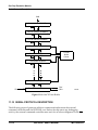
TRIPLE TIMER MODULE . . . . . . . . . . . . . . . . . . . . 9-1
9.1
INTRODUCTION . . . . . . . . . . . . . . . . . . . . . . . . . . . . . . . . . . 9-3
9.2
TRIPLE TIMER MODULE ARCHITECTURE . . . . . . . . . . . . 9-3
9.2.1
Triple Timer Module Block Diagram . . . . . . . . . . . . . . . . . 9-3
9.2.2
Timer Block Diagram. . . . . . . . . . . . . . . . . . . . . . . . . . . . . 9-4
9.3
TRIPLE TIMER MODULE PROGRAMMING MODEL. . . . . . 9-5
9.3.1
Prescaler Counter . . . . . . . . . . . . . . . . . . . . . . . . . . . . . . . 9-7
9.3.2
Timer Prescaler Load Register (TPLR). . . . . . . . . . . . . . . 9-7
9.3.2.1
TPLR Prescaler Preload Value (PL[20:0]) Bits 20–0 . . 9-7
9.3.2.2
TPLR Prescaler Source (PS[1:0]) Bits 22–21. . . . . . . . 9-7
9.3.2.3
TPLR Reserved Bit 23 . . . . . . . . . . . . . . . . . . . . . . . . . 9-8
9.3.3
Timer Prescaler Count Register (TPCR). . . . . . . . . . . . . . 9-8
9.3.3.1
TPCR Prescaler Counter Value (PC[20:0]) Bits 20–0 . 9-9
9.3.3.2
TPCR Reserved Bits 23–21 . . . . . . . . . . . . . . . . . . . . . 9-9
9.3.4
Timer Control/Status Register (TCSR) . . . . . . . . . . . . . . . 9-9
9.3.4.1
Timer Enable (TE) Bit 0 . . . . . . . . . . . . . . . . . . . . . . . . 9-9
9.3.4.2
Timer Overflow Interrupt Enable (TOIE) Bit 1. . . . . . . . 9-9
9.3.4.3
Timer Compare Interrupt Enable (TCIE) Bit 2 . . . . . . . 9-9
9.3.4.4
Timer Control (TC[3:0]) Bits 4–7. . . . . . . . . . . . . . . . . 9-10
9.3.4.5
Inverter (INV) Bit 8 . . . . . . . . . . . . . . . . . . . . . . . . . . . 9-11
9.3.4.6
Timer Reload Mode (TRM) Bit 9. . . . . . . . . . . . . . . . . 9-13
9.3.4.7
Direction (DIR) Bit 11 . . . . . . . . . . . . . . . . . . . . . . . . . 9-13
9.3.4.8
Data Input (DI) Bit 12 . . . . . . . . . . . . . . . . . . . . . . . . . 9-13
9.3.4.9
Data Output (DO) Bit 13 . . . . . . . . . . . . . . . . . . . . . . . 9-13
9.3.4.10
Prescaler Clock Enable (PCE) Bit 15 . . . . . . . . . . . . . 9-14
9.3.4.11
Timer Overflow Flag (TOF) Bit 20 . . . . . . . . . . . . . . . 9-14
9.3.4.12
Timer Compare Flag (TCF) Bit 21 . . . . . . . . . . . . . . . 9-14
9.3.4.13
TCSR Reserved Bits 3, 10, 14, 16–19, 22, 23 . . . . . . 9-14
9.3.5
Timer Load Register (TLR) . . . . . . . . . . . . . . . . . . . . . . . 9-14
9.3.6
Timer Compare Register (TCPR) . . . . . . . . . . . . . . . . . . 9-15
x
DSP56307 User’s Manual
MOTOROLA
9.3.7
Timer Count Register (TCR) . . . . . . . . . . . . . . . . . . . . . . 9-15
9.4
TIMER MODES OF OPERATION . . . . . . . . . . . . . . . . . . . . 9-16
9.4.1
Timer Modes . . . . . . . . . . . . . . . . . . . . . . . . . . . . . . . . . . 9-16
9.4.1.1
Timer GPIO (Mode 0) . . . . . . . . . . . . . . . . . . . . . . . . . 9-17
9.4.1.2
Timer Pulse (Mode 1) . . . . . . . . . . . . . . . . . . . . . . . . . 9-17
9.4.1.3
Timer Toggle (Mode 2) . . . . . . . . . . . . . . . . . . . . . . . . 9-18
9.4.1.4
Timer Event Counter (Mode 3) . . . . . . . . . . . . . . . . . . 9-19
9.4.2
Signal Measurement Modes . . . . . . . . . . . . . . . . . . . . . . 9-20
9.4.2.1
Measurement Accuracy . . . . . . . . . . . . . . . . . . . . . . . 9-20
9.4.2.2
Measurement Input Width (Mode 4) . . . . . . . . . . . . . . 9-20
9.4.2.3
Measurement Input Period (Mode 5) . . . . . . . . . . . . . 9-21
9.4.2.4
Measurement Capture (Mode 6) . . . . . . . . . . . . . . . . . 9-22
9.4.3
Pulse Width Modulation (PWM, Mode 7) . . . . . . . . . . . . . 9-23
9.4.4
Watchdog Modes . . . . . . . . . . . . . . . . . . . . . . . . . . . . . . . 9-24
9.4.4.1
Watchdog Pulse (Mode 9). . . . . . . . . . . . . . . . . . . . . . 9-24
9.4.4.2
Watchdog Toggle (Mode 10). . . . . . . . . . . . . . . . . . . . 9-24
9.4.5
Reserved Modes . . . . . . . . . . . . . . . . . . . . . . . . . . . . . . . 9-26
9.4.6
Special Cases . . . . . . . . . . . . . . . . . . . . . . . . . . . . . . . . . 9-26
9.4.6.1
Timer Behavior during Wait. . . . . . . . . . . . . . . . . . . . . 9-26
9.4.6.2
Timer Behavior during Stop . . . . . . . . . . . . . . . . . . . . 9-26
9.4.7
DMA Trigger . . . . . . . . . . . . . . . . . . . . . . . . . . . . . . . . . . 9-26
SECTION 10 ENHANCED FILTER COPROCESSOR . . . . . . . . 10-1
10.1
INTRODUCTION TO EFCOP. . . . . . . . . . . . . . . . . . . . . . . . 10-3
10.2
KEY FEATURES . . . . . . . . . . . . . . . . . . . . . . . . . . . . . . . . . 10-3
10.3
GENERAL DESCRIPTION. . . . . . . . . . . . . . . . . . . . . . . . . . 10-4
10.3.1
PMB Interface . . . . . . . . . . . . . . . . . . . . . . . . . . . . . . . . . 10-5
10.3.2
EFCOP Memory Banks . . . . . . . . . . . . . . . . . . . . . . . . . . 10-7
10.3.3
Filter Multiplier and Accumulator (FMAC) . . . . . . . . . . . . 10-8
10.4
EFCOP PROGRAMMING MODEL . . . . . . . . . . . . . . . . . . . 10-9
10.4.1
Filter Data Input Register (FDIR) . . . . . . . . . . . . . . . . . . . 10-9
10.4.2
Filter Data Output Register (FDOR) . . . . . . . . . . . . . . . 10-10
10.4.3
Filter K-Constant Input Register (FKIR) . . . . . . . . . . . . . 10-10
10.4.4
Filter Count (FCNT) Register . . . . . . . . . . . . . . . . . . . . . 10-10
10.4.5
EFCOP Control Status Register (FCSR) . . . . . . . . . . . . 10-11
10.4.6
EFCOP ALU Control Register (FACR) . . . . . . . . . . . . . 10-16
MOTOROLA
DSP56307 User’s Manual
xi
10.4.7
10.4.8
10.4.9
10.4.10
EFCOP Data Base Address (FDBA). . . . . . . . . . . . . . .
EFCOP Coefficient Base Address (FCBA) . . . . . . . . . .
Decimation/Channel Count Register (FDCH) . . . . . . . .
EFCOP Interrupt Vectors . . . . . . . . . . . . . . . . . . . . . . .
10-17
10-18
10-18
10-19
SECTION 11 ON-CHIP EMULATION MODULE. . . . . . . . . . . . . 11-1
11.1
INTRODUCTION . . . . . . . . . . . . . . . . . . . . . . . . . . . . . . . . . 11-3
11.2
ONCE MODULE SIGNALS . . . . . . . . . . . . . . . . . . . . . . . . . 11-3
11.3
DEBUG EVENT . . . . . . . . . . . . . . . . . . . . . . . . . . . . . . . . . . 11-4
11.4
ONCE CONTROLLER. . . . . . . . . . . . . . . . . . . . . . . . . . . . . 11-4
11.4.1
OnCE Command Register (OCR) . . . . . . . . . . . . . . . . . . 11-5
11.4.1.1
Register Select (RS4–RS0) Bits 0–4 . . . . . . . . . . . . . 11-5
11.4.1.2
Exit Command (EX) Bit 5 . . . . . . . . . . . . . . . . . . . . . . 11-7
11.4.1.3
GO Command (GO) Bit 6 . . . . . . . . . . . . . . . . . . . . . . 11-7
11.4.1.4
Read/Write Command (R/W) Bit 7 . . . . . . . . . . . . . . . 11-7
11.4.2
OnCE Decoder (ODEC) . . . . . . . . . . . . . . . . . . . . . . . . . 11-8
11.4.3
OnCE Status and Control Register (OSCR) . . . . . . . . . . 11-8
11.4.3.1
Trace Mode Enable (TME) Bit 0 . . . . . . . . . . . . . . . . . 11-8
11.4.3.2
Interrupt Mode Enable (IME) Bit 1 . . . . . . . . . . . . . . . 11-8
11.4.3.3
Software Debug Occurrence (SWO) Bit 2 . . . . . . . . . 11-8
11.4.3.4
Memory Breakpoint Occurrence (MBO) Bit 3 . . . . . . . 11-8
11.4.3.5
Trace Occurrence (TO) Bit 4 . . . . . . . . . . . . . . . . . . . 11-9
11.4.3.6
Reserved OCSR Bit 5 . . . . . . . . . . . . . . . . . . . . . . . . 11-9
11.4.3.7
Core Status (OS0, OS1) Bits 6–7. . . . . . . . . . . . . . . . 11-9
11.4.3.8
Reserved Bits 8–23 . . . . . . . . . . . . . . . . . . . . . . . . . . 11-9
11.5
ONCE MEMORY BREAKPOINT LOGIC. . . . . . . . . . . . . . . 11-9
11.5.1
OnCE Memory Address Latch (OMAL). . . . . . . . . . . . . 11-11
11.5.2
OnCE Memory Limit Register 0 (OMLR0). . . . . . . . . . . 11-11
11.5.3
OnCE Memory Address Comparator 0 (OMAC0) . . . . . 11-11
11.5.4
OnCE Memory Limit Register 1 (OMLR1). . . . . . . . . . . 11-11
11.5.5
OnCE Memory Address Comparator 1 (OMAC1) . . . . . 11-11
11.5.6
OnCE Breakpoint Control Register (OBCR) . . . . . . . . . 11-11
11.5.6.1
Memory Breakpoint Select (MBS0–MBS1) . . . . . . . 11-12
11.5.6.2
Breakpoint 0 Read/Write Select (RW00–RW01) . . . 11-12
11.5.6.3
Breakpoint 0 Condition Code Select (CC00–CC01). 11-13
11.5.6.4
Breakpoint 1 Read/Write Select (RW10–RW11) . . . 11-13
xii
DSP56307 User’s Manual
MOTOROLA
11.5.6.5
Breakpoint 1 Condition Code Select (CC10–CC11) . 11-14
11.5.6.6
Breakpoint 0 and 1 Event Select (BT0–BT1) . . . . . . 11-14
11.5.6.7
OnCE Memory Breakpoint Counter (OMBC) . . . . . . 11-14
11.5.6.8
Reserved Bits 12–15. . . . . . . . . . . . . . . . . . . . . . . . . 11-15
11.6
ONCE TRACE LOGIC . . . . . . . . . . . . . . . . . . . . . . . . . . . . 11-15
11.7
METHODS OF ENTERING DEBUG MODE . . . . . . . . . . . 11-16
11.7.1
External Debug Request during RESET Assertion . . . . 11-16
11.7.2
External Debug Request during Normal Activity . . . . . . 11-16
11.7.3
Executing the JTAG DEBUG_REQUEST Instruction . . 11-17
11.7.4
External Debug Request during Stop . . . . . . . . . . . . . . 11-17
11.7.5
External Debug Request during Wait . . . . . . . . . . . . . . 11-17
11.7.6
Software Request during Normal Activity . . . . . . . . . . . 11-17
11.7.7
Enabling Trace Mode. . . . . . . . . . . . . . . . . . . . . . . . . . . 11-18
11.7.8
Enabling Memory Breakpoints . . . . . . . . . . . . . . . . . . . . 11-18
11.8
PIPELINE INFORMATION AND OGDB REGISTER . . . . . 11-18
11.8.1
OnCE PDB Register (OPDBR) . . . . . . . . . . . . . . . . . . . 11-19
11.8.2
OnCE PIL Register (OPILR) . . . . . . . . . . . . . . . . . . . . . 11-19
11.8.3
OnCE GDB Register (OGDBR) . . . . . . . . . . . . . . . . . . . 11-19
11.9
TRACE BUFFER . . . . . . . . . . . . . . . . . . . . . . . . . . . . . . . . 11-20
11.9.1
OnCE PAB Register for Fetch (OPABFR) . . . . . . . . . . . 11-20
11.9.2
PAB Register for Decode (OPABDR) . . . . . . . . . . . . . . 11-20
11.9.3
OnCE PAB Register for Execute (OPABEX) . . . . . . . . . 11-20
11.9.4
Trace Buffer . . . . . . . . . . . . . . . . . . . . . . . . . . . . . . . . . . 11-21
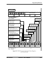
11.10 SERIAL PROTOCOL DESCRIPTION . . . . . . . . . . . . . . . . 11-22
11.11 TARGET SITE DEBUG SYSTEM REQUIREMENTS . . . . 11-23
11.12 EXAMPLES OF USING THE ONCE . . . . . . . . . . . . . . . . . 11-23
11.12.1
Checking Whether the Chip Has Entered Debug Mode 11-24
11.12.2
Polling the JTAG Instruction Shift Register . . . . . . . . . . 11-24
11.12.3
Saving Pipeline Information . . . . . . . . . . . . . . . . . . . . . . 11-24
11.12.4
Reading the Trace Buffer. . . . . . . . . . . . . . . . . . . . . . . . 11-25
11.12.5
Displaying a Specified Register . . . . . . . . . . . . . . . . . . . 11-26
11.12.6
Displaying X Memory Area Starting at Address $xxxx . 11-26
11.12.7
Returning from Debug to Normal Mode (Same Program)11-27
11.12.8
Returning from Debug to Normal Mode (New Program) 11-28
11.13 EXAMPLES OF JTAG AND ONCE INTERACTION. . . . . . 11-28
MOTOROLA
DSP56307 User’s Manual
xiii
SECTION 12 JOINT TEST ACTION GROUP PORT . . . . . . . . . 12-1
12.1
INTRODUCTION TO THE JTAG PORT . . . . . . . . . . . . . . . 12-3
12.2
JTAG SIGNALS . . . . . . . . . . . . . . . . . . . . . . . . . . . . . . . . . . 12-4
12.2.1
Test Clock (TCK). . . . . . . . . . . . . . . . . . . . . . . . . . . . . . . 12-5
12.2.2
Test Mode Select (TMS) . . . . . . . . . . . . . . . . . . . . . . . . . 12-5
12.2.3
Test Data Input (TDI) . . . . . . . . . . . . . . . . . . . . . . . . . . . 12-5
12.2.4
Test Data Output (TDO) . . . . . . . . . . . . . . . . . . . . . . . . . 12-5
12.2.5
Test Reset (TRST) . . . . . . . . . . . . . . . . . . . . . . . . . . . . . 12-5
12.3
TAP CONTROLLER . . . . . . . . . . . . . . . . . . . . . . . . . . . . . . 12-6
12.3.1
Boundary Scan Register . . . . . . . . . . . . . . . . . . . . . . . . . 12-7
12.3.2
Instruction Register . . . . . . . . . . . . . . . . . . . . . . . . . . . . . 12-7
12.3.2.1
EXTEST (B[3:0] = 0000). . . . . . . . . . . . . . . . . . . . . . . 12-8
12.3.2.2
SAMPLE/PRELOAD (B[3:0] = 0001) . . . . . . . . . . . . . 12-9
12.3.2.3
IDCODE (B[3:0] = 0010). . . . . . . . . . . . . . . . . . . . . . . 12-9
12.3.2.4
CLAMP (B[3:0] = 0011) . . . . . . . . . . . . . . . . . . . . . . 12-10
12.3.2.5
HI-Z (B[3:0] = 0100) . . . . . . . . . . . . . . . . . . . . . . . . . 12-10
12.3.2.6
ENABLE_ONCE(B[3:0] = 0110) . . . . . . . . . . . . . . . . 12-11
12.3.2.7
DEBUG_REQUEST(B[3:0] = 0111) . . . . . . . . . . . . . 12-11
12.3.2.8
BYPASS (B[3:0] = 1111) . . . . . . . . . . . . . . . . . . . . . 12-11
12.4
DSP56300 RESTRICTIONS . . . . . . . . . . . . . . . . . . . . . . . 12-12
12.5
DSP56307 BOUNDARY SCAN REGISTER . . . . . . . . . . . 12-13
APPENDICES:
A
BOOTSTRAP PROGRAMS
B
EQUATES
C
DSP56307 BSDL LISTING
D
EFCOP PROGRAMMING
E
PROGRAMMING REFERENCE
xiv
DSP56307 User’s Manual
MOTOROLA
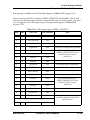
LIST OF FIGURES
Figure 1-1
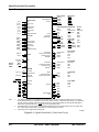
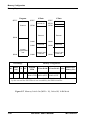
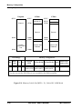
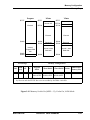
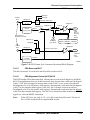
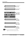
DSP56307 Block Diagram. . . . . . . . . . . . . . . . . . . . . . . . . . . . . 1-14
Figure 2-1
Signals Identified by Functional Group . . . . . . . . . . . . . . . . . . . . 2-4
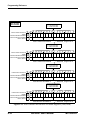
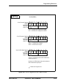
Figure 3-1
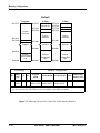
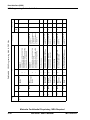
Memory Switch Off, Cache Off, 24-Bit Mode (default) . . . . . . . 3-12
Figure 3-2
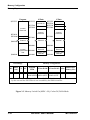
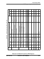
Memory Switch Off, Cache On, 24-Bit Mode . . . . . . . . . . . . . . 3-13
Figure 3-3
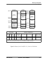
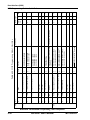
Memory Switch On (MSW = 00), Cache Off, 24-Bit Mode . . . . 3-14
Figure 3-4
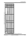
Memory Switch On (MSW = 00), Cache On, 24-Bit Mode . . . . 3-15
Figure 3-5
Memory Switch On (MSW = 01), Cache Off, 24-Bit Mode . . . . 3-16
Figure 3-6
Memory Switch On (MSW = 01), Cache On, 24-Bit Mode . . . . 3-17
Figure 3-7
Memory Switch On (MSW = 10), Cache Off, 24-Bit Mode . . . . 3-18
Figure 3-8
Memory Switch On (MSW = 10), Cache On, 24-Bit Mode . . . . 3-19
Figure 3-9
Memory Switch On (MSW = 11), Cache Off, 24-Bit Mode . . . . 3-20
Figure 3-10
Memory Switch On (MSW = 11), Cache On, 24-Bit Mode . . . . 3-21
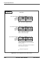
Figure 3-11
Memory Switch Off, Cache Off, 16-Bit Mode . . . . . . . . . . . . . . 3-22
Figure 3-12
Memory Switch Off, Cache On, 16-Bit Mode . . . . . . . . . . . . . . 3-23
Figure 3-13
Memory Switch On (MSW = 00), Cache Off, 16-Bit Mode . . . . 3-24
Figure 3-14
Memory Switch On (MSW = 00), Cache On, 16-Bit Mode . . . . 3-25
Figure 3-15
Memory Switch On (MSW = 01), Cache Off, 16-Bit Mode . . . . 3-26
Figure 3-16
Memory Switch On (MSW = 01), Cache On, 16-Bit Mode . . . . 3-27
Figure 3-17
Memory Switch On (MSW = 10), Cache Off, 16-Bit Mode . . . . 3-28
MOTOROLA
DSP56307 User’s Manual
xv
Figure 3-18
Memory Switch On (MSW = 10), Cache On, 16-Bit Mode . . . . 3-29
Figure 3-19
Memory Switch On (MSW = 11), Cache Off, 16-Bit Mode . . . . 3-30
Figure 3-20
Memory Switch On (MSW = 11), Cache On, 16-Bit Mode . . . . 3-31
Figure 4-1
Interrupt Priority Register C (IPR-C) (X:$FFFFFF). . . . . . . . . . . 4-12
Figure 4-2
Interrupt Priority Register P (IPR-P) (X:$FFFFFE). . . . . . . . . . . 4-12
Figure 4-3
DSP56307 Operating Mode Register (OMR) Format. . . . . . . . . 4-16
Figure 4-4
PLL Control Register (PCTL) . . . . . . . . . . . . . . . . . . . . . . . . . . . 4-17
Figure 4-5
Identification Register Configuration (Revision 0) . . . . . . . . . . . 4-18
Figure 4-6
Address Attribute Registers (AAR0–AAR3) . . . . . . . . . . . . . . . . 4-19
Figure 4-7
JTAG Identification Register Configuration (Revision 0) . . . . . . 4-20
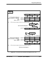
Figure 6-1
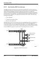
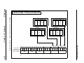
HI08 Block Diagram . . . . . . . . . . . . . . . . . . . . . . . . . . . . . . . . . . . 6-7
Figure 6-2
Host Control Register (HCR) (X:$FFFFC2) . . . . . . . . . . . . . . . . . 6-9
Figure 6-3
Host Status Register (HSR) (X:$FFFFC3) . . . . . . . . . . . . . . . . . 6-11
Figure 6-4
Host Base Address Register (HBAR) (X:$FFFFC5). . . . . . . . . . 6-12
Figure 6-5
Self Chip Select Logic . . . . . . . . . . . . . . . . . . . . . . . . . . . . . . . . 6-13
Figure 6-6
Host Port Control Register (HPCR) (X:$FFFFC4) . . . . . . . . . . . 6-13
Figure 6-7
Single Strobe Bus. . . . . . . . . . . . . . . . . . . . . . . . . . . . . . . . . . . . 6-16
Figure 6-8
Dual Strobe Bus . . . . . . . . . . . . . . . . . . . . . . . . . . . . . . . . . . . . . 6-16
Figure 6-9
Host Data Direction Register (HDDR) (X:$FFFFC8) . . . . . . . . . 6-17
Figure 6-10
Host Data Register (HDR) (X:$FFFFC9) . . . . . . . . . . . . . . . . . . 6-18
Figure 6-11
HSR-HCR Operation . . . . . . . . . . . . . . . . . . . . . . . . . . . . . . . . . 6-20
Figure 6-12
Interface Control Register (ICR). . . . . . . . . . . . . . . . . . . . . . . . . 6-22
xvi
DSP56307 User’s Manual
MOTOROLA
Figure 6-13
Command Vector Register (CVR) . . . . . . . . . . . . . . . . . . . . . . . 6-25
Figure 6-14
Interface Status Register . . . . . . . . . . . . . . . . . . . . . . . . . . . . . . 6-26
Figure 6-15
Interrupt Vector Register (IVR) . . . . . . . . . . . . . . . . . . . . . . . . . 6-28
Figure 6-16
HI08 Host Request Structure. . . . . . . . . . . . . . . . . . . . . . . . . . . 6-32
Figure 7-1
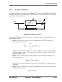
ESSI Block Diagram . . . . . . . . . . . . . . . . . . . . . . . . . . . . . . . . . . 7-5
Figure 7-2
ESSI Control Register A (CRA) . . . . . . . . . . . . . . . . . . . . . . . . . . 7-9
Figure 7-3
ESSI Control Register B (CRB) . . . . . . . . . . . . . . . . . . . . . . . . . . 7-9
Figure 7-4
ESSI Status Register (SSISR). . . . . . . . . . . . . . . . . . . . . . . . . . . 7-9
Figure 7-5
ESSI Transmit Slot Mask Register A (TSMA) . . . . . . . . . . . . . . 7-10
Figure 7-6
ESSI Transmit Slot Mask Register B (TSMB) . . . . . . . . . . . . . . 7-10
Figure 7-7
ESSI Receive Slot Mask Register A (RSMA) . . . . . . . . . . . . . . 7-10
Figure 7-8
ESSI Receive Slot Mask Register B (RSMB) . . . . . . . . . . . . . . 7-10
Figure 7-9
ESSI Clock Generator Functional Block Diagram . . . . . . . . . . . 7-12
Figure 7-10
ESSI Frame Sync Generator Functional Block Diagram. . . . . . 7-13
Figure 7-11
CRB FSL0 and FSL1 Bit Operation (FSR = 0) . . . . . . . . . . . . . 7-19
Figure 7-12
CRB SYN Bit Operation. . . . . . . . . . . . . . . . . . . . . . . . . . . . . . . 7-20
Figure 7-13
CRB MOD Bit Operation . . . . . . . . . . . . . . . . . . . . . . . . . . . . . . 7-21
Figure 7-14
Normal Mode, External Frame Sync (8 Bit, 1 Word in Frame) . 7-22
Figure 7-15
Network Mode, External Frame Sync (8 Bit, 2 Words in Frame) 7-23
Figure 7-16
ESSI Data Path Programming Model (SHFD = 0). . . . . . . . . . . 7-30
Figure 7-17
ESSI Data Path Programming Model (SHFD = 1). . . . . . . . . . . 7-31
Figure 7-18
Port Control Register (PCR) (PCRC X:$FFFFBF). . . . . . . . . . . 7-43
MOTOROLA
DSP56307 User’s Manual
xvii
Figure 7-19
Port Direction Register (PRR)(PRRC X:$FFFFBE) . . . . . . . . . . 7-44
Figure 7-20
Port Data Register (PDR) (PDRC X:$FFFFBD) . . . . . . . . . . . . . 7-45
Figure 8-1
SCI Control Register (SCR) . . . . . . . . . . . . . . . . . . . . . . . . . . . . . 8-5
Figure 8-2
SCI Status Register (SSR) . . . . . . . . . . . . . . . . . . . . . . . . . . . . . . 8-5
Figure 8-3
SCI Clock Control Register (SCCR). . . . . . . . . . . . . . . . . . . . . . . 8-5
Figure 8-5
16 x Serial Clock . . . . . . . . . . . . . . . . . . . . . . . . . . . . . . . . . . . . 8-16
Figure 8-6
SCI Baud Rate Generator . . . . . . . . . . . . . . . . . . . . . . . . . . . . . 8-18
Figure 8-7
SCI Programming Model - Data Registers . . . . . . . . . . . . . . . . . 8-19
Figure 8-8
Port E Control Register (PCRE) . . . . . . . . . . . . . . . . . . . . . . . . . 8-27
Figure 8-9
Port E Direction Register (PRRE) . . . . . . . . . . . . . . . . . . . . . . . 8-28
Figure 8-10
Port E Data Register (PDRE) . . . . . . . . . . . . . . . . . . . . . . . . . . . 8-29
Figure 9-1
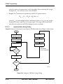
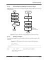
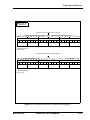
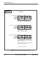
Triple Timer Module Block Diagram . . . . . . . . . . . . . . . . . . . . . . . 9-4
Figure 9-2
Timer Module Block Diagram . . . . . . . . . . . . . . . . . . . . . . . . . . . . 9-5
Figure 9-3
Timer Module Programmer’s Model . . . . . . . . . . . . . . . . . . . . . . . 9-6
Figure 9-4
Timer Prescaler Load Register (TPLR) . . . . . . . . . . . . . . . . . . . . 9-7
Figure 9-5
Timer Prescaler Count Register (TPCR) . . . . . . . . . . . . . . . . . . . 9-8
Figure 10-1
EFCOP Block Diagram. . . . . . . . . . . . . . . . . . . . . . . . . . . . . . . . 10-5
Figure 10-2
EFCOP Register Layout. . . . . . . . . . . . . . . . . . . . . . . . . . . . . . . 10-5
Figure 10-3
Storage of Filter Coefficients . . . . . . . . . . . . . . . . . . . . . . . . . . . 10-7
Figure 10-4
EFCOP Memory Organization . . . . . . . . . . . . . . . . . . . . . . . . . . 10-8
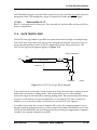
Figure 11-1
OnCE Module Block Diagram . . . . . . . . . . . . . . . . . . . . . . . . . . 11-3
Figure 11-2
OnCE Module Multiprocessor Configuration . . . . . . . . . . . . . . . 11-4
xviii
DSP56307 User’s Manual
MOTOROLA
Figure 11-3
OnCE Controller Block Diagram . . . . . . . . . . . . . . . . . . . . . . . . 11-5
Figure 11-4
OnCE Command Register. . . . . . . . . . . . . . . . . . . . . . . . . . . . . 11-5
Figure 11-5
OnCE Status and Control Register (OSCR) . . . . . . . . . . . . . . . 11-8
Figure 11-6
OnCE Memory Breakpoint Logic 0 . . . . . . . . . . . . . . . . . . . . . 11-10
Figure 11-7
OnCE Breakpoint Control Register (OBCR) . . . . . . . . . . . . . . 11-12
Figure 11-8
OnCE Trace Logic Block Diagram. . . . . . . . . . . . . . . . . . . . . . 11-15
Figure 11-9
OnCE Pipeline Information and GDB Registers . . . . . . . . . . . 11-19
Figure 11-10
OnCE Trace Buffer . . . . . . . . . . . . . . . . . . . . . . . . . . . . . . . . . 11-22
Figure 12-1
TAP Block Diagram . . . . . . . . . . . . . . . . . . . . . . . . . . . . . . . . . . 12-4
Figure 12-2
TAP Controller State Machine . . . . . . . . . . . . . . . . . . . . . . . . . . 12-6
Figure 12-3
JTAG Instruction Register . . . . . . . . . . . . . . . . . . . . . . . . . . . . . 12-7
Figure 12-4
JTAG ID Register . . . . . . . . . . . . . . . . . . . . . . . . . . . . . . . . . . . 12-9
Figure 12-5
BYPASS Register . . . . . . . . . . . . . . . . . . . . . . . . . . . . . . . . . . 12-11
MOTOROLA
DSP56307 User’s Manual
xix
xx
DSP56307 User’s Manual
MOTOROLA
LIST OF TABLES
Table 1-1
High True/Low True Signal Conventions. . . . . . . . . . . . . . . . . . . 1-5
Table 1-2
Available Memory Configurations . . . . . . . . . . . . . . . . . . . . . . . 1-12
Table 2-1
DSP56307 Functional Signal Groupings . . . . . . . . . . . . . . . . . . 2-3
Table 2-2
Power Inputs . . . . . . . . . . . . . . . . . . . . . . . . . . . . . . . . . . . . . . . . 2-5
Table 2-3
Grounds. . . . . . . . . . . . . . . . . . . . . . . . . . . . . . . . . . . . . . . . . . . . 2-6
Table 2-4
Clock Signals . . . . . . . . . . . . . . . . . . . . . . . . . . . . . . . . . . . . . . . 2-7
Table 2-5
Phase-Locked Loop Signals . . . . . . . . . . . . . . . . . . . . . . . . . . . . 2-7
Table 2-6
External Address Bus Signals . . . . . . . . . . . . . . . . . . . . . . . . . . . 2-8
Table 2-7
External Data Bus Signals. . . . . . . . . . . . . . . . . . . . . . . . . . . . . . 2-9
Table 2-8
External Bus Control Signals . . . . . . . . . . . . . . . . . . . . . . . . . . . 2-9
Table 2-9
Interrupt and Mode Control . . . . . . . . . . . . . . . . . . . . . . . . . . . . 2-13
Table 2-10
Host Interface . . . . . . . . . . . . . . . . . . . . . . . . . . . . . . . . . . . . . . 2-16
Table 2-11
Enhanced Synchronous Serial Interface 0 . . . . . . . . . . . . . . . . 2-22
Table 2-12
Enhanced Serial Synchronous Interface 1 . . . . . . . . . . . . . . . . 2-25
Table 2-13
Serial Communication Interface . . . . . . . . . . . . . . . . . . . . . . . . 2-28
Table 2-14
Triple Timer Signals . . . . . . . . . . . . . . . . . . . . . . . . . . . . . . . . . 2-30
Table 2-15
OnCE/JTAG Interface . . . . . . . . . . . . . . . . . . . . . . . . . . . . . . . . 2-32
Table 4-1
DSP56307 Operating Modes . . . . . . . . . . . . . . . . . . . . . . . . . . 4-4
Table 4-2
Interrupt Sources . . . . . . . . . . . . . . . . . . . . . . . . . . . . . . . . . . . 4-10
MOTOROLA
DSP56307 User’s Manual
xxi
Table 4-3
Interrupt Priority Level Bits . . . . . . . . . . . . . . . . . . . . . . . . . . . . . 4-13
Table 4-4
Interrupt Source Priorities within an IPL . . . . . . . . . . . . . . . . . . 4-13
Table 4-5
DMA Request Sources . . . . . . . . . . . . . . . . . . . . . . . . . . . . . . . 4-15
Table 6-1
HI08 Signal Definitions for Various Operational Modes . . . . . . . . 6-6
Table 6-2
HI08 Data Strobe Signals. . . . . . . . . . . . . . . . . . . . . . . . . . . . . . . 6-6
Table 6-3
HI08 Host Request Signals . . . . . . . . . . . . . . . . . . . . . . . . . . . . . 6-6
Table 6-4
Host Command Interrupt Priority List . . . . . . . . . . . . . . . . . . . . . 6-10
Table 6-5
HDR and HDDR Functionality . . . . . . . . . . . . . . . . . . . . . . . . . . 6-18
Table 6-6
DSP Side Registers after Reset . . . . . . . . . . . . . . . . . . . . . . . . . 6-19
Table 6-7
Host Side Register Map . . . . . . . . . . . . . . . . . . . . . . . . . . . . . . . 6-22
Table 6-8
TREQ and RREQ modes (HDRQ = 0) . . . . . . . . . . . . . . . . . . . . 6-23
Table 6-9
TREQ and RREQ modes (HDRQ = 1) . . . . . . . . . . . . . . . . . . . . 6-23
Table 6-10
INIT Command Effects . . . . . . . . . . . . . . . . . . . . . . . . . . . . . . . . 6-24
Table 6-11
HREQ and HDRQ Settings . . . . . . . . . . . . . . . . . . . . . . . . . . . . 6-28
Table 6-12
Host Side Registers after Reset . . . . . . . . . . . . . . . . . . . . . . . . . 6-30
Table 6-13
Host Control Register (HCR) . . . . . . . . . . . . . . . . . . . . . . . . . . . 6-34
Table 6-14
HI08 Programming Model: DSP Side. . . . . . . . . . . . . . . . . . . . . 6-35
Table 6-15
HI08 Programming Model: Host Side. . . . . . . . . . . . . . . . . . . . . 6-38
Table 7-1
ESSI Clock Sources . . . . . . . . . . . . . . . . . . . . . . . . . . . . . . . . . . . 7-8
Table 7-2
ESSI Word Length Selection . . . . . . . . . . . . . . . . . . . . . . . . . . . 7-14
Table 7-3
FSL1 and FSL0 Encoding . . . . . . . . . . . . . . . . . . . . . . . . . . . . . 7-17
Table 7-4
Mode and Signal Definition Table
xxii
. . . . . . . . . . . . . . . . . . . . . . 7-24
DSP56307 User’s Manual
MOTOROLA
Table 7-5
Port Control Register and Port Direction Register Bits . . . . . . . 7-44
Table 8-1
Word Formats . . . . . . . . . . . . . . . . . . . . . . . . . . . . . . . . . . . . . . . 8-8
Table 8-2
TCM and RCM Bit Configuration . . . . . . . . . . . . . . . . . . . . . . . . 8-17
Table 8-3
SCI Registers after Reset . . . . . . . . . . . . . . . . . . . . . . . . . . . . . 8-23
Table 8-4
Port Control Register and Port Direction Register Bits . . . . . . . 8-28
Table 9-1
Prescaler Source Selection . . . . . . . . . . . . . . . . . . . . . . . . . . . . . 9-8
Table 9-2
Timer Control Bits . . . . . . . . . . . . . . . . . . . . . . . . . . . . . . . . . . . 9-10
Table 9-3
Inverter (INV) Bit Operation . . . . . . . . . . . . . . . . . . . . . . . . . . . . 9-11
Table 10-1
EFCOP Register Descriptions . . . . . . . . . . . . . . . . . . . . . . . . . 10-6
Table 10-2
EFCOP Registers and Base Addresses . . . . . . . . . . . . . . . . . . 10-9
Table 10-3
FCNT Register Bit Descriptions. . . . . . . . . . . . . . . . . . . . . . . . 10-11
Table 10-4
FCSR Bit Descriptions . . . . . . . . . . . . . . . . . . . . . . . . . . . . . . 10-12
Table 10-5
FACR Bit Description. . . . . . . . . . . . . . . . . . . . . . . . . . . . . . . . 10-17
Table 10-6
FDCH Register Bit Descriptions . . . . . . . . . . . . . . . . . . . . . . . 10-20
Table 10-7
EFCOP Interrupt Vectors. . . . . . . . . . . . . . . . . . . . . . . . . . . . . 10-21
Table 10-8
EFCOP DMA Request Sources. . . . . . . . . . . . . . . . . . . . . . . . 10-21
Table 11-1
OnCE Register Select Encoding . . . . . . . . . . . . . . . . . . . . . . . 11-6
Table 11-2
EX Bit Definition. . . . . . . . . . . . . . . . . . . . . . . . . . . . . . . . . . . . . 11-7
Table 11-3
GO Bit Definition . . . . . . . . . . . . . . . . . . . . . . . . . . . . . . . . . . . . 11-7
Table 11-4
R/W Bit Definition . . . . . . . . . . . . . . . . . . . . . . . . . . . . . . . . . . . 11-7
Table 11-5
Core Status Bits Description . . . . . . . . . . . . . . . . . . . . . . . . . . . 11-9
Table 11-6
Memory Breakpoint 0 and 1 Select . . . . . . . . . . . . . . . . . . . . . 11-12
MOTOROLA
DSP56307 User’s Manual
xxiii
Table 11-7
Breakpoint 0 Read/Write Select . . . . . . . . . . . . . . . . . . . . . . . 11-13
Table 11-8
Breakpoint 0 Condition Select . . . . . . . . . . . . . . . . . . . . . . . . . 11-13
Table 11-9
Breakpoint 1 Read/Write Select . . . . . . . . . . . . . . . . . . . . . . . 11-13
Table 11-10
Breakpoint 1 Condition Select Table . . . . . . . . . . . . . . . . . . . . 11-14
Table 11-11
Breakpoint 0 and 1 Event Select Table . . . . . . . . . . . . . . . . . . 11-14
Table 11-12
TMS Sequencing for DEBUG_REQUEST . . . . . . . . . . . . . . . 11-29
Table 11-13
TMS Sequencing for ENABLE_ONCE . . . . . . . . . . . . . . . . . . . 11-30
Table 11-14
TMS Sequencing for Reading Pipeline Registers
Table 12-1
JTAG Instructions. . . . . . . . . . . . . . . . . . . . . . . . . . . . . . . . . . . . 12-8
Table 12-2
DSP56306 BSR Bit Definitions. . . . . . . . . . . . . . . . . . . . . . . . . 12-13
xxiv
DSP56307 User’s Manual
. . . . . . . . . 11-30
MOTOROLA
SECTION 1
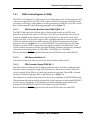
OVERVIEW
MOTOROLA
DSP56307 User’s Manual
1-1
Overview
1.1
1.2
1.3
1.4
1.5
1.6
1.7
1.8
1.9
1.10
1-2
INTRODUCTION . . . . . . . . . . . . . . . . . . . . . . . . . . . . . . . . . . . . 1-3
MANUAL ORGANIZATION . . . . . . . . . . . . . . . . . . . . . . . . . . . . 1-3
MANUAL CONVENTIONS . . . . . . . . . . . . . . . . . . . . . . . . . . . . 1-4
FEATURES . . . . . . . . . . . . . . . . . . . . . . . . . . . . . . . . . . . . . . . . 1-6
CORE DESCRIPTION. . . . . . . . . . . . . . . . . . . . . . . . . . . . . . . . 1-7
DSP56300 CORE FUNCTIONAL BLOCKS . . . . . . . . . . . . . . . 1-7
INTERNAL BUSES . . . . . . . . . . . . . . . . . . . . . . . . . . . . . . . . . 1-13
BLOCK DIAGRAM. . . . . . . . . . . . . . . . . . . . . . . . . . . . . . . . . . 1-14
DMA. . . . . . . . . . . . . . . . . . . . . . . . . . . . . . . . . . . . . . . . . . . . . 1-15
ARCHITECTURE. . . . . . . . . . . . . . . . . . . . . . . . . . . . . . . . . . . 1-15
DSP56307 User’s Manual
MOTOROLA
Overview
Introduction
1.1
INTRODUCTION
This manual describes the DSP56307 24-bit digital signal processor (DSP), its memory,
operating modes, and peripheral modules. The DSP56307 is an implementation of the
DSP56300 core with a unique configuration of on-chip memory, cache, and peripherals.
This manual is to be used with the DSP56300 Family Manual (DSP56300FM/AD), which
describes the CPU, core programming models, and instruction set details. DSP56307
Technical Data (DSP56307/D)—referred to as the data sheet—provides electrical
specifications, timing, pinout, and packaging descriptions of the DSP56307.
You can obtain these documents, as well as Motorola’s DSP development tools, through
a local Motorola Semiconductor Sales Office or authorized distributor.
To receive the latest information on this DSP, access the Motorola DSP home page at the
address given on the back cover of this document.
1.2
MANUAL ORGANIZATION
This manual contains the following sections and appendices:
• Section 1 Overview provides a brief description of the DSP56307, including a
features list and block diagram, lists related documentation needed to use this
chip, and describes the organization of this manual.
• Section 2 Signal/Connection Descriptions describes the DSP56307 signals and
their functional groupings.
• Section 3 Memory Configuration describes the DSP56307 memory spaces, RAM
configuration, memory configuration bit settings, memory configurations, and
memory maps.
• Section 4 Core Configuration describes the registers for configuring the
DSP56300 core when programming the DSP56307, in particular the interrupt
vector locations and the operation of the interrupt priority registers, and explains
the operating modes and how they affect the processor’s program and data
memories.
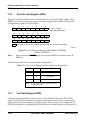
• Section 5 GeneraL-Purpose Input/Output describes the DSP56307
general-purpose input/output (GPIO) capability and the programming model for
the GPIO signals (operation, registers, and control).
• Section 6 Host Interface (HI08) describes the 8-bit host interface (HI08),
including a quick reference to the HI08 programming model.
MOTOROLA
DSP56307 User’s Manual
1-3
Overview
Manual Conventions
• Section 7 Enhanced Synchronous Serial Interface describes the 24-bit ESSI,
which provides two identical full duplex UART-style serial ports for
communications with devices such as codecs, DSPs, microprocessors, and
peripherals implementing the Motorola serial peripheral interface (SPI) protocol.
• Section 8 Serial Communication Interface describes the 24-bit SCI, a full duplex
serial port for serial communication to DSPs, microcontrollers, or other
peripherals (such as modems or other RS-232 devices).
• Section 9 Triple Timer Module describes the three identical devices that may be
used as internals or event counters.
• Section 10 Enhanced Filter Coprocessor describes the echo cancellation and
filtering coprocessor.
• Section 11 On-Chip Emulation Module describes the On-Chip Emulation
(OnCE™) module, which is accessed through the joint test action group (JTAG)
port.
• Section 12 Joint Test Action Group Port describes the specifics of the JTAG port
on the DSP56307.
• Appendix Overview lists the bootstrap code used for the DSP56307.
• Appendix B Equates lists the equates (I/O, HI08, SCI, ESSI, exception
processing, timer, direct memory access (DMA), phase-locked loop (PLL), BIU,
and interrupts for the DSP56307.
• Appendix C DSP56307 BSDL Listing provides the BSDL listing for the
DSP56307.
• Appendix D EFCOP Programming describes the two types of digital filters
supported by the enhanced filter coprocessor (EFCOP) and provides examples of
how to use them.
• Appendix E Programming Reference lists peripheral addresses, interrupt
addresses, and interrupt priorities for the DSP56307 and contains programming
sheets listing the contents of the major DSP56307 registers for programmer’s
reference.
1.3
MANUAL CONVENTIONS
This manual uses the following conventions:
• Bits within registers are always listed from most significant bit (MSB) to least
significant bit (LSB).
1-4
DSP56307 User’s Manual
MOTOROLA
Overview
Manual Conventions
• Bits within a register are indicated AA[n:m], n > m, when more than one bit is
involved in a description. For purposes of description, the bits are presented as if
they are contiguous within a register. However, this is not always the case. Refer
to the programming model diagrams or to the programmer’s sheets to see the
exact location of bits within a register.
• When a bit is described as “set,” its value is 1. When a bit is described as
“cleared,” its value is 0.
• The word “assert” means that a high true (active high) signal is pulled high to
VCC or that a low true (active low) signal is pulled low to ground. The word
“deassert” means that a high true signal is pulled low to ground or that a low true
signal is pulled high to VCC. See Table 1-1.
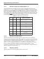
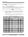
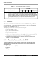
Table 1-1 High True/Low True Signal Conventions
1.
2.
3.
Signal/Symbol
Logic State
Signal State
Voltage
PIN1
True
Asserted
Ground2
PIN
False
Deasserted
VCC3
PIN
True
Asserted
VCC
PIN
False
Deasserted
Ground
PIN is a generic term for any pin on the chip.
Ground is an acceptable low voltage level. See the appropriate data sheet for the range of
acceptable low voltage levels (typically a TTL logic low).
VCC is an acceptable high voltage level. See the appropriate data sheet for the range of
acceptable high voltage levels (typically a TTL logic high).
• Pins or signals that are asserted low (made active when pulled to ground) are
indicated like this in text:
–
In text, they have an overbar: for example, RESET is asserted low.
–
In code examples, they have a tilde in front of their names. In Example 1-1,
line 3 refers to the SS0 signal (shown as ~SS0).
• Sets of signals are indicated by the first and last signals in the set, for instance
HA1–HA8.
• “Input/Output” indicates a bidirectional signal. “Input or Output” indicates a
signal that is exclusively one or the other.
MOTOROLA
DSP56307 User’s Manual
1-5
Overview
Features
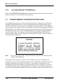
• Code examples are displayed in a monospaced font, as shown in Example 1-1.
Example 1-1 Sample Code Listing
BFSET
#$0007,X:PCC; Configure:
line
1
;
MISO0, MOSI0, SCK0 for SPI master
; ~SS0 as PC3 for GPIO
line 2
line 3
• Hex values are indicated with a dollar sign ($) preceding the hex value, as
follows: $FFFFFF is the X memory address for the core interrupt priority register.
• The word “reset” is used in four different contexts in this manual:
1.4
–
the reset signal, written as RESET,
–
the reset instruction, written as RESET,
–
the reset operating state, written as Reset, and
–
the reset function, written as reset.
FEATURES
Motorola developed the DSP56307, a member of the DSP56300 core family of
programmable DSPs, to support wireless infrastructure applications with general
filtering operations. The on-chip EFCOP processes filter algorithms in parallel with core
operation, thus increasing overall DSP performance and efficiency. Like the other family
members, the DSP56307 uses a high-performance, single-clock-cycle-per-instruction
engine (code compatible with Motorola's popular DSP56000 core family), a barrel shifter,
24-bit addressing, instruction cache, and DMA controller. The DSP56307 offers 100
million instructions per second (MIPS) performance using an internal 100 MHz clock
with 2.5 V core and independent 3.3 V input/output (I/O) power.
All DSP56300 core family members contain the DSP56300 core and additional modules.
The modules are chosen from a library of standard predesigned elements, such as
memories and peripherals. New modules may be added to the library to meet customer
specifications. A standard interface between the DSP56300 core and the on-chip memory
and peripherals supports a wide variety of memory and peripheral configurations. In
particular, the DSP56307 includes Motorola’s JTAG port as well as Motorola’s OnCE
module.
1-6
DSP56307 User’s Manual
MOTOROLA
Overview
Core Description
The DSP56307, with its large on-chip memory array of 64K words and its EFCOP, is well
suited for high-end multichannel telecommunication applications, such as wireless
infrastructure, multi-line voice/data/fax processing, video conferencing, and general
digital signal processing.
1.5
CORE DESCRIPTION
Core features are described fully in the DSP56300 Family Manual. (This manual, in
contrast, documents pinout, memory, and peripheral features.)
• 100 MIPS with a 100 MHz clock at 3.3 V
• Object code compatible with the DSP56000 core
• Highly parallel instruction set
• Large on-chip RAM memory of 64K words
• EFCOP running concurrently with the core, capable of executing 100 million filter
taps per second at peak performance
• Hardware debugging support
–
JTAG test access port (TAP)
–
OnCE module
–
Address trace mode reflects internal accesses at the external port
• Reduced power dissipation
1.6
–
Very low-power CMOS design
–
Wait and stop low-power standby modes
–
Fully-static logic, operation frequency down to 0 Hz (dc)
–
Optimized power-management circuitry (instruction-dependent,
peripheral-dependent, and mode-dependent)
DSP56300 CORE FUNCTIONAL BLOCKS
The DSP56300 core provides the following functional blocks:
• Data arithmetic logic unit (ALU)
• Address generation unit
MOTOROLA
DSP56307 User’s Manual
1-7
Overview
DSP56300 Core Functional Blocks
• Program control unit
• PLL and clock oscillator
• JTAG TAP and OnCE module
• Memory
In addition, the DSP56307 provides a set of on-chip peripherals, shown in Section 1.8.
1.6.1
Data ALU
The data ALU performs all the arithmetic and logical operations on data operands in the
DSP56300 core. These are the components of the data ALU:
• Fully pipelined 24 × 24-bit parallel multiplier-accumulator
• Bit field unit, comprising a 56-bit parallel barrel shifter (fast shift and
normalization; bit stream generation and parsing)
• Conditional ALU instructions
• Software-controllable 24-bit or 16-bit arithmetic support
• Four 24-bit input general purpose registers: X1, X0, Y1, and Y0
• Six data ALU registers (A2, A1, A0, B2, B1, and B0) that are concatenated into two
general purpose, 56-bit accumulators, A and B, accumulator shifters
• Two data bus shifter/limiter circuits
1.6.1.1
Data ALU Registers
The data ALU registers can be read or written over the X data bus and the Y data bus as
16- or 32-bit operands. The source operands for the data ALU, which can be 16, 32, or 40
bits, always originate from data ALU registers. The results of all data ALU operations
are stored in an accumulator.
All the data ALU operations are performed in two clock cycles in pipeline fashion so that
a new instruction can be initiated in every clock cycle, yielding an effective execution
rate of one instruction per clock cycle. The destination of every arithmetic operation can
be used as a source operand for the immediate following operation without penalty.
1.6.1.2
Multiplier-Accumulator (MAC)
The MAC unit comprises the main arithmetic processing unit of the DSP56300 core and
performs all of the calculations on data operands. In the case of arithmetic instructions,
the unit accepts as many as three input operands and outputs one 56-bit result of the
1-8
DSP56307 User’s Manual
MOTOROLA
Overview
DSP56300 Core Functional Blocks
following form: extension:most significant product:least significant product
(EXT:MSP:LSP).
The multiplier executes 24-bit × 24-bit, parallel, fractional multiplies between
two’s-complement signed, unsigned, or mixed operands. The 48-bit product is
right-justified and added to the 56-bit contents of either the A or B accumulator. A 56-bit
result can be stored as a 24-bit operand. The LSP can either be truncated or rounded into
the MSP. Rounding is performed if specified.
1.6.2
Address Generation Unit (AGU)
The AGU performs the effective address calculations using integer arithmetic necessary
to address data operands in memory and contains the registers that generate the
addresses. It implements four types of arithmetic: linear, modulo, multiple wrap-around
modulo, and reverse-carry. The AGU operates in parallel with other chip resources to
minimize address-generation overhead.
The AGU is divided into two halves, each with its own address ALU. Each address ALU
has four sets of register triplets, and each register triplet is composed of an address
register, an offset register, and a modifier register. The two address ALUs are identical.
Each contains a 16-bit full adder (called an offset adder).
A second full adder (called a modulo adder) adds the summed result of the first full
adder to a modulo value that is stored in its respective modifier register. A third full
adder (called a reverse-carry adder) is also provided.
The offset adder and the reverse-carry adder work in parallel and share common inputs.
The only difference between them is that the carry propagates in opposite directions.
Test logic determines which of the three summed results of the full adders is output.
Each address ALU can update one address register from its own address register file
during one instruction cycle. The contents of the associated modifier register specifies
the type of arithmetic to be used in the address register update calculation. The modifier
value is decoded in the address ALU.
1.6.3
Program Control Unit (PCU)
The PCU performs instruction prefetch, instruction decoding, hardware DO loop
control, and exception processing. The PCU implements a seven-stage pipeline and
MOTOROLA
DSP56307 User’s Manual
1-9
Overview
DSP56300 Core Functional Blocks
controls the different processing states of the DSP56300 core. The PCU consists of three
hardware blocks:
• Program decode controller
• Program address generator
• Program interrupt controller
The program decode controller decodes the 24-bit instruction loaded into the instruction
latch and generates all signals necessary for pipeline control. The program address
generator contains all the hardware needed for program address generation, system
stack, and loop control. The program interrupt controller arbitrates among all interrupt
requests (internal interrupts, as well as the five external requests IRQA, IRQB, IRQC,
IRQD, and NMI), and generates the appropriate interrupt vector address.
PCU features include the following:
• Position-independent code support
• Addressing modes optimized for DSP applications (including immediate offsets)
• On-chip instruction cache controller
• On-chip memory-expandable hardware stack
• Nested hardware DO loops
• Fast auto-return interrupts
The PCU implements its functions using the following registers:
• Program counter register
• Status register
• Loop address register
• Loop counter register
• Vector base address register
• Size register
• Stack pointer
• Operating mode register
• Stack counter register
The PCU also includes a hardware system stack.
1-10
DSP56307 User’s Manual
MOTOROLA
Overview
DSP56300 Core Functional Blocks
1.6.4
PLL and Clock Oscillator
The clock generator in the DSP56300 core comprises two main blocks: the PLL, which
performs clock input division, frequency multiplication, and skew elimination; and the
clock generator, which performs low-power division and clock pulse generation.
These features allow you to do the following:
• Change the low-power divide factor without losing the lock.
• Output a clock with skew elimination.
The PLL allows the processor to operate at a high internal clock frequency using a
low-frequency clock input, a feature that offers two immediate benefits:
• A lower-frequency clock input reduces the overall electromagnetic interference
generated by a system.
• The ability to oscillate at different frequencies reduces costs by eliminating the
need to add additional oscillators to a system.
1.6.5
JTAG TAP and OnCE Module
The DSP56300 core provides a dedicated user-accessible TAP that is fully compatible
with the IEEE 1149.1 Standard Test Access Port and Boundary Scan Architecture.
Problems associated with testing high-density circuit boards have led to development of
this standard under the sponsorship of the Test Technology Committee of IEEE and the
JTAG. The DSP56300 core implementation supports circuit-board test strategies based
on this standard.
The test logic includes a TAP consisting of four dedicated signals, a 16-state controller,
and three test data registers. A boundary scan register links all device signals into a
single shift register. The test logic, implemented utilizing static logic design, is
independent of the device system logic. More information about the JTAG port is
provided in Section 12 Joint Test Action Group Port on page 12-1.
The OnCE module provides a means of interacting with the DSP56300 core and its
peripherals nonintrusively so that a user can examine registers, memory, or on-chip
peripherals. This facilitates hardware and software development on the DSP56300 core
processor. OnCE module functions are provided through the JTAG TAP signals. More
information on the OnCE module is provided in Section 11 On-Chip Emulation
Module on page 11-1.
MOTOROLA
DSP56307 User’s Manual
1-11
Overview
DSP56300 Core Functional Blocks
1.6.6
On-Chip Memory
The memory space of the DSP56300 core is partitioned into program memory space,
X data memory space, and Y data memory space. The data memory space is divided into
X data memory and Y data memory in order to work with the two address ALUs and to
feed two operands simultaneously to the data ALU. Memory space includes internal
RAM and ROM and can be expanded off-chip under software control. More information
about the internal memory is provided in Section 3 Memory Configuration on page 3-1.
Program RAM, instruction cache, X data RAM, and Y data RAM size are programmable,
as shown in Table 1-2:
Table 1-2 Available Memory Configurations
Program RAM
Size
Instruction
Cache Size
X Data RAM
Size*
Y Data RAM
Size*
Instruction
Cache
Switch
Mode
M1
M0
16K × 24-bit
0
24K × 24-bit
24K × 24-bit
disabled
disabled
0/1
0/1
15K × 24-bit
1024 × 24-bit
24K × 24-bit
24K × 24-bit
enabled
disabled
0/1
0/1
48K × 24-bit
0
8K × 24-bit
8K × 24-bit
disabled
enabled
0
0
47K × 24-bit
1024 × 24-bit
8K × 24-bit
8K × 24-bit
enabled
enabled
0
0
40K × 24-bit
0
12K × 24-bit
12K × 24-bit
disabled
enabled
0
1
39K × 24-bit
1024 × 24-bit
12K × 24-bit
12K × 24-bit
enabled
enabled
0
1
32K × 24-bit
0
16K × 24-bit
16K × 24-bit
disabled
enabled
1
0
31K × 24-bit
1024 × 24-bit
16K × 24-bit
16K × 24-bit
enabled
enabled
1
0
24K × 24-bit
0
20K × 24-bit
20K × 24-bit
disabled
enabled
1
1
23K × 24-bit
1024 × 24-bit
20K × 24-bit
20K × 24-bit
enabled
enabled
1
1
*Includes 4K × 24-bit shared memory (i.e., memory shared by the core and the EFCOP and not accessible
by the DMA controller)
There is an on-chip 192 x 24-bit bootstrap ROM.
1.6.7
Off-Chip Memory Expansion
Memory can be expanded off chip to the following capacities:
• Data memory expansion to two 16 M × 24-bit word memory spaces in 24-bit
address mode (64K in 16-bit address mode)
• Program memory expansion to one 16 M × 24-bit word memory space in 24-bit
address mode (64K in 16-bit address mode)
Further features of off-chip memory include the following:
• External memory expansion port
1-12
DSP56307 User’s Manual
MOTOROLA
Overview
Internal Buses
• Simultaneous glueless interface to static RAM (SRAM) and dynamic RAM
(DRAM)
1.7
INTERNAL BUSES
To provide data exchange between these blocks, the DSP56307 implements the following
buses:
• Peripheral I/O expansion bus to peripherals
• Program memory expansion bus to program ROM
• X memory expansion bus to X memory
• Y memory expansion bus to Y memory
• Global data bus between PCU and other core structures
• Program data bus for carrying program data throughout the core
• X memory data bus for carrying X data throughout the core
• Y memory data bus for carrying Y data throughout the core
• Program address bus for carrying program memory addresses throughout the
core
• X memory address bus for carrying X memory addresses throughout the core
• Y memory address bus for carrying Y memory addresses throughout the core.
The block diagram in Figure 1-1 illustrates those buses among other components.
MOTOROLA
DSP56307 User’s Manual
1-13
Overview
Block Diagram
1.8
BLOCK DIAGRAM
With the exception of the program data bus, all internal buses on the DSP56300 family
members are 24-bit buses. The program data bus is also a 24-bit bus. Figure 1-1 shows a
block diagram of the DSP56307.
3
16
6
6
Memory Expansion Area
EFCOP
PIO_EB
Peripheral
Expansion Area
Address
Generation
Unit
Six Channel
DMA Unit
DDB
YDB
XDB
PDB
GDB
Internal
Data
Bus
Switch
EXTAL
XTAL
RESET
PINIT/NMI
YAB
XAB
PAB
DAB
Y Data
RAM
24K ¥ 24
24-Bit
DSP56300
Core
Bootstrap
ROM
Clock
Generator
X Data
RAM
24K ¥ 24
YM_EB
ESSI
Interface
Program
RAM
16K ¥ 24 or
(Program
RAM
15K ¥ 24 and
Instruction
Cache
1024 ¥ 24)
XM_EB
Triple
Timer
Enhanced
Filtering
Coprocessor
PM_EB
SCI
Interface
Host
Interface
HI08
Program
Interrupt
Controller
PLL
2
Program
Decode
Controller
Program
Address
Generator
External
Address
Bus
Switch
External
Bus
Interface
and
I - Cache
Control
External
Data
Bus
Switch
Data ALU
24 ¥ 24+56Æ56-bit MAC
Two 56-bit Accumulators
56-bit Barrel Shifter
MODA/IRQA
MODB/IRQB
MODC/IRQC
MODD/IRQD
Power
Mngmnt.
18
Address
13
Control
24
Data
5
JTAG
OnCE™
DE
AA1367
Figure 1-1 DSP56307 Block Diagram
Note:
1-14
See Section 1.6.6 On-Chip Memory on page 1-12 for details about memory
size.
DSP56307 User’s Manual
MOTOROLA
Overview
DMA
1.9
DMA
The DMA block has the following features:
• Six DMA channels supporting internal and external accesses
• One-, two-, and three-dimensional transfers (including circular buffering)
• End-of-block-transfer interrupts
• Triggering from interrupt lines and all peripherals
1.10
ARCHITECTURE
Motorola designed the DSP56307 to perform a wide variety of fixed-point digital signal
processing functions. In addition to the core features previously discussed, the
DSP56307 provides the following peripherals:
• As many as 34 user-configurable GPIO signals
• HI08 to external hosts
• Dual ESSI
• SCI
• Triple timer module
• Memory switch mode
• Four external interrupt/mode control lines
1.10.1
GPIO Functionality
The GPIO port consists of as many as 34 programmable signals, all of which are also
used by the peripherals (HI08, ESSI, SCI, and timer). There are no dedicated GPIO
signals. After a reset, the signals are automatically configured as GPIO. Three
memory-mapped registers per peripheral control GPIO functionality. The techniques to
use when programming these registers to control GPIO functionality are detailed in
Section 5 GeneraL-Purpose Input/Output .
MOTOROLA
DSP56307 User’s Manual
1-15
Overview
Architecture
1.10.2
HI08
The HI08 is a byte-wide, full-duplex, double-buffered, parallel port that can connect
directly to the data bus of a host processor. The HI08 supports a variety of buses and
provides connection with a number of industry-standard DSPs, microcomputers, and
microprocessors without requiring any additional logic. The DSP core treats the HI08 as
a memory-mapped peripheral occupying eight 24-bit words in data memory space. The
DSP can use the HI08 as a memory-mapped peripheral, using either standard polled or
interrupt programming techniques. Separate transmit and receive data registers are
double-buffered to allow the DSP and host processor to transfer data efficiently at high
speed. Memory mapping allows you to program DSP core communication with the HI08
registers by using standard instructions and addressing modes.
1.10.3
ESSI
The DSP56307 provides two independent and identical ESSI. Each ESSI provides a
full-duplex serial port for communication with a variety of serial devices, including one
or more industry-standard codecs, other DSPs, microprocessors, and peripherals that
implement the Motorola SPI. The ESSI consists of independent transmitter and receiver
sections and a common ESSI clock generator.
The capabilities of the ESSI include the following:
• Independent (asynchronous) or shared (synchronous) transmit and receive
sections with separate or shared internal/external clocks and frame syncs
• Normal mode operation using frame sync
• Network mode operation with as many as 32 time slots
• Programmable word length (8, 12, or 16 bits)
• Program options for frame synchronization and clock generation
•
1-16
One receiver and three transmitters per ESSI
DSP56307 User’s Manual
MOTOROLA
Overview
Architecture
1.10.4
SCI
The DSP56307’s SCI provides a full-duplex port for serial communication with other
DSPs, microprocessors, or peripherals such as modems. The SCI interfaces without
additional logic to peripherals that use TTL-level signals. With a small amount of
additional logic, the SCI can connect to peripheral interfaces that have non-TTL level
signals, such as the RS-232C, RS-422, etc.
This interface uses three dedicated signals: transmit data, receive data, and SCI serial
clock. It supports industry-standard asynchronous bit rates and protocols, as well as
high-speed synchronous data transmission (up to 12.5 Mbps for a 100 MHz clock). The
asynchronous protocols supported by the SCI include a multidrop mode for
master/slave operation with wakeup on idle line and wakeup on address bit capability.
This mode allows the DSP56307 to share a single serial line efficiently with other
peripherals.
The SCI consists of separate transmit and receive sections that can operate
asynchronously with respect to each other. A programmable baud-rate generator
provides the transmit and receive clocks. An enable vector and an interrupt vector have
been included so that the baud-rate generator can function as a general purpose timer
when it is not being used by the SCI or when the interrupt timing is the same as that
used by the SCI.
1.10.5
Timer Module
The triple timer module is composed of a common 21-bit prescaler and three
independent and identical general purpose 24-bit timer/event counters, each one having
its own memory-mapped register set. Each timer has a single signal that can function as
a GPIO signal or as a timer signal. Each timer can use internal or external clocking and
can interrupt the DSP after a specified number of events (clocks) or signal an external
device after counting internal events. Each timer connects to the external world through
one bidirectional signal. When this signal is configured as an input, the timer can
function as an external event counter or measures external pulse width/signal period.
When the signal is used as an output, the timer can function as either a timer, a
watchdog, or a pulse width modulator.
MOTOROLA
DSP56307 User’s Manual
1-17
Overview
Architecture
1.10.6
EFCOP
The EFCOP is a peripheral block interfacing with the DSP core via the peripheral
module bus. The EFCOP is a general-purpose, fully programmable coprocessor
designed to perform filtering tasks concurrently with the DSP core with minimum core
overhead. The DSP core and the EFCOP can share data by means of an 8K-word shared
data memory. DMA channels shuttle input and output data between the DSP core and
the EFCOP.
The EFCOP supports a variety of filter modes, some of which are optimized for cellular
base station applications:
• Real finite impulse response (FIR) with real taps
• Complex FIR with complex taps
• Complex FIR generating pure real or pure imaginary outputs alternately
• A 4-bit decimation factor in FIR filters, thus providing a decimation ratio up to 16
• Direct form 1 (DFI) infinite impulse response (IIR) filter
• Direct form 2 (DFII) IIR filter
• Four scaling factors (1, 4, 8, 16) for IIR output
• Adaptive FIR filter with true least mean square (LMS) coefficient updates
• Adaptive FIR filter with delayed LMS coefficient updates
The EFCOP supports up to 4K taps and 4K coefficients in any combination of number
and length of filters (e.g., eight filters of length 512, or 16 filters of length 256). It can
perform either 24-bit or 16-bit precision arithmetic with full support for saturation
arithmetic.
The EFCOP is a cost-effective and power-efficient coprocessor that accelerates filtering
tasks, such as echo cancellation or correlation, concurrently with software running on
the DSP core.
1-18
DSP56307 User’s Manual
MOTOROLA
SECTION 2
2
SIGNAL/CONNECTION
DESCRIPTIONS
MOTOROLA
DSP56307 User’s Manual
2-1
Signal/Connection Descriptions
2.1
2.2
2.3
2.4
2.5
2.6
2.7
2.8
2.9
2.10
2.11
2.12
2.13
2-2
SIGNAL GROUPINGS. . . . . . . . . . . . . . . . . . . . . . . . . . . . . . . . 2-3
POWER . . . . . . . . . . . . . . . . . . . . . . . . . . . . . . . . . . . . . . . . . . . 2-5
GROUND. . . . . . . . . . . . . . . . . . . . . . . . . . . . . . . . . . . . . . . . . . 2-6
CLOCK . . . . . . . . . . . . . . . . . . . . . . . . . . . . . . . . . . . . . . . . . . . 2-7
PLL . . . . . . . . . . . . . . . . . . . . . . . . . . . . . . . . . . . . . . . . . . . . . . 2-7
EXTERNAL MEMORY EXPANSION PORT (PORT A). . . . . . . 2-8
INTERRUPT AND MODE CONTROL . . . . . . . . . . . . . . . . . . . 2-13
HI08 . . . . . . . . . . . . . . . . . . . . . . . . . . . . . . . . . . . . . . . . . . . . . 2-16
ENHANCED SYNCHRONOUS SERIAL INTERFACE 0
(ESSI0) . . . . . . . . . . . . . . . . . . . . . . . . . . . . . . . . . . . . . . . . . . 2-22
ENHANCED SYNCHRONOUS SERIAL INTERFACE 1
(ESSI1) . . . . . . . . . . . . . . . . . . . . . . . . . . . . . . . . . . . . . . . . . . 2-25
SCI. . . . . . . . . . . . . . . . . . . . . . . . . . . . . . . . . . . . . . . . . . . . . . 2-28
TIMERS . . . . . . . . . . . . . . . . . . . . . . . . . . . . . . . . . . . . . . . . . . 2-30
JTAG AND OnCE INTERFACE. . . . . . . . . . . . . . . . . . . . . . . . 2-31
DSP56307 User’s Manual
MOTOROLA
Signal/Connection Descriptions
Signal Groupings
2.1
SIGNAL GROUPINGS
The DSP56307 input and output signals are organized into functional groups, as shown
in Table 2-1 and as illustrated in Figure 2-1.
Table 2-1 DSP56307 Functional Signal Groupings
Number of
Signals
Detailed
Description
Power (VCC)
20
Figure 2-2
Ground (GND)
19
Figure 2-3
Clock
2
Figure 2-4
PLL
3
Figure 2-5
18
Figure 2-6
24
Figure 2-7
Bus control
13
Figure 2-8
Interrupt and mode control
5
Figure 2-9
Functional Group
Address bus
Port A
Data bus
1
HI08
Port B2
16
Figure 2-10
ESSI
Ports C and D3
12
Figure 2-11 and
Figure 2-12
SCI
Port E4
3
Figure 2-13
Timer5
3
Figure 2-14
OnCE/JTAG Port
6
Figure 2-15
Note:
1.
2.
3.
4.
5.
Port A signals define the external memory interface port, including the external address bus,
data bus, and control signals. The data bus lines have internal keepers.
Port B signals are the HI08 port signals multiplexed with the GPIO signals. All Port B signals
have keepers.
Port C and D signals are the two ESSI port signals multiplexed with the GPIO signals. All
Port C and D signals have keepers.
Port E signals are the SCI port signals multiplexed with the GPIO signals. All Port C signals
have keepers.
All timer signals have keepers.
Figure 2-1 is a diagram of DSP56307 signals by functional group.
MOTOROLA
DSP56307 User’s Manual
2-3
Signal/Connection Descriptions
Signal Groupings
DSP56307
VCCP
VCCQL
VCCQH
VCCA
VCCD
VCCC
VCCH
VCCS
GNDP
GNDP1
GNDQ
GNDA
GNDD
GNDC
GNDH
GNDS
4
3
3
4
2
2
Grounds:
PLL
PLL
Internal Logic
Address Bus
Data Bus
Bus Control
HI08
ESSI/SCI/Timer
4
4
4
2
2
EXTAL
XTAL
During
Reset
PINIT
Power Inputs:
PLL
Core Logic
I/O
Address Bus
Data Bus
Bus Control
HI08
ESSI/SCI/Timer
Clock
CLKOUT
PCAP
After
Reset
NMI
Interrupt/Mode
Control
8
Host
Interface
(HI08) Port1
Enhanced
Synchronous Serial
Interface Port 0
(ESSI0)2
3
Enhanced
Synchronous Serial
Interface Port 1
(ESSI1)2
3
During Reset
MODA
MODB
MODC
MODD
RESET
After Reset
IRQA
IRQB
IRQC
IRQD
RESET
Non-Multiplexed
Bus
H0–H7
HA0
HA1
HA2
HCS/HCS
Single DS
HRW
HDS/HDS
Single HR
HREQ/HREQ
HACK/HACK
Multiplexed
Bus
HAD0–HAD7
HAS/HAS
HA8
HA9
HA10
Double DS
HRD/HRD
HWR/HWR
Double HR
HTRQ/HTRQ
HRRQ/HRRQ
SC00–SC02
SCK0
SRD0
STD0
Port C GPIO
PC0–PC2
PC3
PC4
PC5
SC10–SC12
SCK1
SRD1
STD1
Port D GPIO
PD0–PD2
PD3
PD4
PD5
RXD
TXD
SCLK
Port E GPIO
PE0
PE1
PE2
PLL
Port B
GPIO
PB0–PB7
PB8
PB9
PB10
PB13
PB11
PB12
PB14
PB15
Port A
A0–A17
D0–D23
AA0–AA3/
RAS0–RAS3
RD
WR
TA
BR
BG
BB
CAS
BCLK
BCLK
Note:
1.
2.
3.
18
24
4
External
Address Bus
External
Data Bus
External
Bus
Control
Serial
Communications
Interface (SCI) Port2
Timers3
TIO0
TIO1
TIO2
Timer GPIO
TIO0
TIO1
TIO2
TCK
TDI
TDO
OnCE/JTAG
TMS
Port
TRST
DE
The HI08 port supports a non-multiplexed or a multiplexed bus, single or double Data Strobe (DS), and single or
double Host Request (HR) configurations. Since each of these modes is configured independently, any combination
of these modes is possible. These HI08 signals can also be configured alternately as GPIO signals (PB0–PB15).
Signals with dual designations (e.g., HAS/HAS) have configurable polarity.
The ESSI0, ESSI1, and SCI signals are multiplexed: ESSI0 with the Port C GPIO signals (PC0–PC5), ESSI1 with
Port D GPIO signals (PD0–PD5), and SCI with Port E GPIO signals (PE0–PE2).
TIO0–TIO2 can be configured as GPIO signals.
AA1502
Figure 2-1 Signals Identified by Functional Group
2-4
DSP56307 User’s Manual
MOTOROLA
Signal/Connection Descriptions
Power
2.2
POWER
Table 2-2 Power Inputs
Power Name
Description
VCCP
PLL Power—VCCP is VCC dedicated for PLL use. The voltage should be
well-regulated and the input should be provided with an extremely low
impedance path to the VCC power rail.
VCCQL
Quiet Core (Low) Power—VCCQL is an isolated power for the core
processing logic. This input must be isolated externally from all other chip
power inputs. The user must provide adequate external decoupling
capacitors.
VCCQH
Quiet External (High) Power—VCCQH is a quiet power source for I/O lines.
This input must be tied externally to all other chip power inputs, except
VCCQL. The user must provide adequate decoupling capacitors.
VCCA
Address Bus Power—VCCA is an isolated power for sections of the address
bus I/O drivers. This input must be tied externally to all other chip power
inputs, except VCCQL. The user must provide adequate external decoupling
capacitors.
VCCD
Data Bus Power—VCCD is an isolated power for sections of the data bus I/O
drivers. This input must be tied externally to all other chip power inputs,
except VCCQL. The user must provide adequate external decoupling
capacitors.
VCCC
Bus Control Power—VCCC is an isolated power for the bus control I/O
drivers. This input must be tied externally to all other chip power inputs,
except VCCQL. The user must provide adequate external decoupling
capacitors.
VCCH
Host Power—VCCH is an isolated power for the HI08 I/O drivers. This
input must be tied externally to all other chip power inputs, except VCCQL.
The user must provide adequate external decoupling capacitors.
VCCS
ESSI, SCI, and Timer Power—VCCS is an isolated power for the ESSI, SCI,
and timer I/O drivers. This input must be tied externally to all other chip
power inputs, except VCCQL. The user must provide adequate external
decoupling capacitors.
MOTOROLA
DSP56307 User’s Manual
2-5
Signal/Connection Descriptions
Ground
2.3
GROUND
Table 2-3 Grounds
Ground
Name
Description
GNDP
PLL Ground—GNDP is ground-dedicated for PLL use. The connection should be
provided with an extremely low-impedance path to ground. VCCP should be
bypassed to GNDP by a 0.47 µF capacitor located as close as possible to the chip
package.
GNDP1
PLL Ground 1—GNDP1 is ground-dedicated for PLL use. The connection should be
provided with an extremely low-impedance path to ground.
GNDQ
Quiet Ground—GNDQ is an isolated ground for the internal processing logic. This
connection must be tied externally to all other chip ground connections. The user
must provide adequate external decoupling capacitors.
GNDA
Address Bus Ground—GNDA is an isolated ground for sections of the address bus
I/O drivers. This connection must be tied externally to all other chip ground
connections. The user must provide adequate external decoupling capacitors. There
are four GNDA connections.
GNDD
Data Bus Ground—GNDD is an isolated ground for sections of the data bus I/O
drivers. This connection must be tied externally to all other chip ground
connections. The user must provide adequate external decoupling capacitors.
GNDC
Bus Control Ground—GNDC is an isolated ground for the bus control I/O drivers.
This connection must be tied externally to all other chip ground connections. The
user must provide adequate external decoupling capacitors.
GNDH
Host Ground—GNDH is an isolated ground for the HI08 I/O drivers. This
connection must be tied externally to all other chip ground connections. The user
must provide adequate external decoupling capacitors.
GNDS
ESSI, SCI, and Timer Ground—GNDS is an isolated ground for the ESSI, SCI, and
timer I/O drivers. This connection must be tied externally to all other chip ground
connections. The user must provide adequate external decoupling capacitors.
2-6
DSP56307 User’s Manual
MOTOROLA
Signal/Connection Descriptions
Clock
2.4
CLOCK
Table 2-4 Clock Signals
Signal
Name
Type
State During
Reset
Signal Description
EXTAL
Input
Input
External Clock/Crystal Input—EXTAL interfaces the
internal crystal oscillator input to an external crystal or
an external clock.
XTAL
Output
Chip-driven
Crystal Output—XTAL connects the internal crystal
oscillator output to an external crystal. If an external
clock is used, leave XTAL unconnected.
2.5
PLL
Table 2-5 Phase-Locked Loop Signals
Signal
Name
PCAP
Type
Input
State During
Reset
Input
Signal Description
PLL Capacitor—PCAP is an input connecting an
off-chip capacitor to the PLL filter. Connect one
capacitor terminal to PCAP and the other terminal to
VCCP.
If the PLL is not used, PCAP may be tied to VCC,
GND, or left floating.
CLKOUT
Output
Chip-driven
Clock Output—CLKOUT provides an output clock
synchronized to the internal core clock phase.
If the PLL is enabled and both the multiplication and
division factors equal one, then CLKOUT is also
synchronized to EXTAL.
If the PLL is disabled, the CLKOUT frequency is half
the frequency of EXTAL.
MOTOROLA
DSP56307 User’s Manual
2-7
Signal/Connection Descriptions
External Memory Expansion Port (Port A)
Table 2-5 Phase-Locked Loop Signals (Continued)
Signal
Name
Type
PINIT
Input
NMI
Input
2.6
State During
Reset
Input
Signal Description
PLL Initial—During assertion of RESET, the value of
PINIT is written into the PLL enable (PEN) bit of the
PLL control (PCTL) register, determining whether
the PLL is enabled or disabled.
Nonmaskable Interrupt—After RESET deassertion
and during normal instruction processing, this
Schmitt-trigger input is the negative-edge-triggered
NMI request internally synchronized to CLKOUT.
EXTERNAL MEMORY EXPANSION PORT (PORT A)
Note:
2.6.1
When the DSP56307 enters a low-power standby mode (stop or wait), it
releases bus mastership and tri-states the relevant Port A signals: A0–A17,
D0–D23, AA0/RAS0–AA3/RAS3, RD, WR, BB, CAS, BCLK, BCLK.
External Address Bus
Table 2-6 External Address Bus Signals
Signal
Name
A0–A17
2-8
Type
Output
State During
Reset
Tri-stated
Signal Description
Address Bus—When the DSP is the bus master,
A0–A17 are active-high outputs that specify the
address for external program and data memory
accesses. Otherwise, the signals are tri-stated. To
minimize power dissipation, A0–A17 do not
change state when external memory spaces are not
being accessed.
DSP56307 User’s Manual
MOTOROLA
Signal/Connection Descriptions
External Memory Expansion Port (Port A)
2.6.2
External Data Bus
Table 2-7 External Data Bus Signals
Signal
Name
Type
D0–D23
2.6.3
Input/
Output
State During
Reset
Tri-stated
Signal Description
Data Bus—When the DSP is the bus master,
D0–D23 are active-high, bidirectional
input/outputs that provide the bidirectional data
bus for external program and data memory
accesses. Otherwise, D0–D23 are tri-stated. These
lines have weak keepers to maintain the last state
even if all drivers are tri-stated.
External Bus Control
Table 2-8 External Bus Control Signals
Signal
Name
AA0–AA3
Type
State During
Reset
Output Tri-stated
Signal Description
Address Attribute—When defined as AA, these signals
can be used as chip selects or additional address lines.
The default use defines a priority scheme under which
only one AA signal can be asserted at a time. Setting the
AA priority disable (APD) bit (Bit 14) of the OMR, the
priority mechanism is disabled and the lines can be
used together as four external lines that can be decoded
externally into 16 chip select signals.
Row Address Strobe—When defined as RAS, these
signals can be used as RAS for DRAM interface. These
signals are tri-statable outputs with programmable
polarity.
RAS0–RAS3 Output
RD
Output Tri-stated
Read Enable—When the DSP is the bus master, RD is
an active-low output that is asserted to read external
memory on the data bus (D0–D23). Otherwise, RD is
tri-stated.
WR
Output Tri-stated
Write Enable—When the DSP is the bus master, WR is
an active-low output that is asserted to write external
memory on the data bus (D0–D23). Otherwise, the
signals are tri-stated.
MOTOROLA
DSP56307 User’s Manual
2-9
Signal/Connection Descriptions
External Memory Expansion Port (Port A)
Table 2-8 External Bus Control Signals (Continued)
Signal
Name
TA
Type
Input
State During
Reset
Signal Description
Ignored Input Transfer Acknowledge—If the DSP56307 is the bus
master and there is no external bus activity, or the
DSP56307 is not the bus master, the TA input is ignored.
The TA input is a data transfer acknowledge (DTACK)
function that can extend an external bus cycle
indefinitely. Any number of wait states (1, 2. . .infinity)
may be added to the wait states inserted by the bus
control register (BCR) by keeping TA deasserted. In
typical operation, TA is deasserted at the start of a bus
cycle, is asserted to enable completion of the bus cycle,
and is deasserted before the next bus cycle. The current
bus cycle completes one clock period after TA is
asserted synchronous to CLKOUT. The number of wait
states is determined by the TA input or by the BCR,
whichever is longer. The BCR can be used to set the
minimum number of wait states in external bus cycles.
In order to use the TA functionality, the BCR must be
programmed to at least one wait state. A zero wait state
access cannot be extended by TA deassertion;
otherwise, improper operation may result. TA can
operate synchronously or asynchronously depending
on the setting of the TAS bit in the OMR.
TA functionality may not be used while performing
DRAM type accesses; otherwise, improper operation
may result.
2-10
DSP56307 User’s Manual
MOTOROLA
Signal/Connection Descriptions
External Memory Expansion Port (Port A)
Table 2-8 External Bus Control Signals (Continued)
Signal
Name
Type
State During
Reset
BR
Output Output
(deasserted)
BG
Input
Signal Description
Bus Request—BR is an active-low output, never
tri-stated. BR is asserted when the DSP requests bus
mastership. BR is deasserted when the DSP no longer
needs the bus. BR may be asserted or deasserted
independently of whether the DSP56307 is a bus master
or a bus slave. Bus “parking” allows BR to be deasserted
even though the DSP56307 is the bus master. (See the
description of bus “parking” in the BB signal
description.) The bus request hole (BRH) bit in the BCR
allows BR to be asserted under software control even
though the DSP does not need the bus. BR is typically
sent to an external bus arbitrator that controls the
priority, parking, and tenure of each master on the same
external bus. BR is only affected by DSP requests for the
external bus, never for the internal bus. During
hardware reset, BR is deasserted and the arbitration is
reset to the bus slave state.
Ignored Input Bus Grant—BG is an active-low input. BG must be
asserted/deasserted synchronous to CLKOUT for
proper operation. BG is asserted by an external bus
arbitration circuit when the DSP56307 becomes the next
bus master. When BG is asserted, the DSP56307 must
wait until BB is deasserted before taking bus
mastership. When BG is deasserted, bus mastership is
typically given up at the end of the current bus cycle.
This may occur in the middle of an instruction that
requires more than one external bus cycle for execution.
The default operation of this bit requires a setup and
hold time as specified in DSP56307 Technical Data (the
data sheet). An alternate mode can be invoked: set the
asynchronous bus arbitration enable (ABE) bit (Bit 13) in
the OMR. When this bit is set, BG and BB are
synchronized internally. This eliminates the respective
setup and hold time requirements but adds a required
delay between the deassertion of an initial BG input and
the assertion of a subsequent BG input.
MOTOROLA
DSP56307 User’s Manual
2-11
Signal/Connection Descriptions
External Memory Expansion Port (Port A)
Table 2-8 External Bus Control Signals (Continued)
Signal
Name
BB
Type
State During
Reset
Input/ Input
Output
Signal Description
Bus Busy—BB is a bidirectional active-low
input/output and must be asserted and deasserted
synchronous to CLKOUT. BB indicates that the bus is
active. Only after BB is deasserted can the pending bus
master become the bus master (and then assert the
signal again). The bus master may keep BB asserted
after ceasing bus activity regardless of whether BR is
asserted or deasserted. Called “bus parking,” this
allows the current bus master to reuse the bus without
rearbitration until another device requires the bus. The
deassertion of BB is done by an “active pull-up” method
(i.e., BB is driven high and then released and held high
by an external pull-up resistor).
The default operation of this bit requires a setup and
hold time as specified in the DSP56307 Technical Data
sheet. An alternate mode can be invoked: set the ABE
bit (Bit 13) in the OMR. When this bit is set, BG and BB
are synchronized internally. See BG for additional
information.
BB requires an external pull-up resistor.
CAS
Output Tri-stated
Column Address Strobe—When the DSP is the bus
master, CAS is an active-low output used by DRAM to
strobe the column address. Otherwise, if the bus
mastership enable (BME) bit in the DRAM control
register is cleared, the signal is tri-stated.
BCLK
Output Tri-stated
Bus Clock—When the DSP is the bus master, BCLK is
an active-high output. BCLK is active as a sampling
signal when the program address tracing mode is
enabled (i.e., the ATE bit in the OMR is set). When
BCLK is active and synchronized to CLKOUT by the
internal PLL, BCLK precedes CLKOUT by one-fourth of
a clock cycle. The BCLK rising edge may be used to
sample the internal program memory access on the
A0–A23 address lines.
BCLK
Output Tri-stated
Bus Clock Not—When the DSP is the bus master, BCLK
is an active-low output and is the inverse of the BCLK
signal. Otherwise, the signal is tri-stated.
2-12
DSP56307 User’s Manual
MOTOROLA
Signal/Connection Descriptions
Interrupt and Mode Control
2.7
INTERRUPT AND MODE CONTROL
The interrupt and mode control signals select the chip’s operating mode as it comes out
of hardware reset. After RESET is deasserted, these inputs are hardware interrupt
request lines.
Table 2-9 Interrupt and Mode Control
Type
State During
Reset
RESET
Input
Input
Reset—RESET is an active-low, Schmitt-trigger input.
Deassertion of RESET is internally synchronized to
CLKOUT. When asserted, the chip is placed in the
Reset state and the internal phase generator is reset.
The Schmitt-trigger input allows a slowly rising input
(such as a capacitor charging) to reset the chip reliably.
If RESET is deasserted synchronous to CLKOUT, exact
start-up timing is guaranteed, allowing multiple
processors to start synchronously and operate
together in “lock-step.” When the RESET signal is
deasserted, the initial chip operating mode is latched
from the MODA, MODB, MODC, and MODD inputs.
The RESET signal must be asserted after power up.
MODA
Input
Input
Mode Select A—MODA is an active-low
Schmitt-trigger input, internally synchronized to
CLKOUT. MODA, MODB, MODC, and MODD select
one of 16 initial chip operating modes, latched into the
OMR when the RESET signal is deasserted.
IRQA
Input
Signal Name
MOTOROLA
Signal Description
External Interrupt Request A—After reset, this input
becomes a level-sensitive or negative-edge-triggered,
maskable interrupt request input during normal
instruction processing. If IRQA is asserted
synchronous to CLKOUT, multiple processors can be
resynchronized using the WAIT instruction and
asserting IRQA to exit the wait state. If the processor is
in the stop standby state and IRQA is asserted, the
processor will exit the stop state.
DSP56307 User’s Manual
2-13
Signal/Connection Descriptions
Interrupt and Mode Control
Table 2-9 Interrupt and Mode Control (Continued)
Type
State During
Reset
MODB
Input
Input
IRQB
Input
MODC
Input
IRQC
Input
Signal Name
2-14
Signal Description
Mode Select B—MODB is an active-low
Schmitt-trigger input, internally synchronized to
CLKOUT. MODA, MODB, MODC, and MODD select
one of 16 initial chip operating modes, latched into the
OMR when the RESET signal is deasserted.
External Interrupt Request B—After reset, this input
becomes a level-sensitive or negative-edge-triggered,
maskable interrupt request input during normal
instruction processing. If IRQB is asserted
synchronous to CLKOUT, multiple processors can be
resynchronized using the WAIT instruction and
asserting IRQB to exit the wait state. If the processor is
in the stop standby state and IRQB is asserted, the
processor will exit the stop state.
Input
Mode Select C—MODC is an active-low
Schmitt-trigger input, internally synchronized to
CLKOUT. MODA, MODB, MODC, and MODD select
one of 16 initial chip operating modes, latched into the
OMR when the RESET signal is deasserted.
External Interrupt Request C—After reset, this input
becomes a level-sensitive or negative-edge-triggered,
maskable interrupt request input during normal
instruction processing. If IRQC is asserted
synchronous to CLKOUT, multiple processors can be
resynchronized using the WAIT instruction and
asserting IRQC to exit the wait state. If the processor is
in the stop standby state and IRQC is asserted, the
processor will exit the stop state.
DSP56307 User’s Manual
MOTOROLA
Signal/Connection Descriptions
Interrupt and Mode Control
Table 2-9 Interrupt and Mode Control (Continued)
Type
State During
Reset
MODD
Input
Input
IRQD
Input
Signal Name
MOTOROLA
Signal Description
Mode Select D—MODD is an active-low
Schmitt-trigger input, internally synchronized to
CLKOUT. MODA, MODB, MODC, and MODD select
one of 16 initial chip operating modes, latched into the
OMR when the RESET signal is deasserted.
External Interrupt Request D—After reset, this input
becomes a level-sensitive or negative-edge-triggered,
maskable interrupt request input during normal
instruction processing. If IRQD is asserted
synchronous to CLKOUT, multiple processors can be
resynchronized using the WAIT instruction and
asserting IRQD to exit the wait state. If the processor is
in the stop standby state and IRQD is asserted, the
processor will exit the stop state.
DSP56307 User’s Manual
2-15
Signal/Connection Descriptions
HI08
2.8
HI08
The HI08 provides a fast parallel-data-to-8-bit port that may be connected directly to the
host bus. The HI08 supports a variety of standard buses and can be directly connected to
a number of industry standard microcomputers, microprocessors, DSPs, and DMA
hardware.
Table 2-10 Host Interface
Signal Name
Type
State
During
Reset
Signal Description
H0–H7
Input/
Output
HAD0–HAD7
Input/
Output
Host Address—When HI08 is programmed to
interface a multiplexed host bus and the HI function
is selected, these signals are lines 0–7 of the
address/data bidirectional, multiplexed, tri-state
bus.
PB0–PB7
Input or
Output
Port B 0–7—When the HI08 is configured as GPIO
through the host port control register (HPCR), these
signals are individually programmed as inputs or
outputs through the HI08 data direction register
(HDDR).
Tri-stated
Host Data—When the HI08 is programmed to
interface a nonmultiplexed host bus and the HI
function is selected, these signals are lines 0–7 of the
data bidirectional, tri-state bus.
Note:
2-16
This signal has a weak keeper to maintain the last state
even if all drivers are tri-stated.
DSP56307 User’s Manual
MOTOROLA
Signal/Connection Descriptions
HI08
Table 2-10 Host Interface (Continued)
Signal Name
Type
State
During
Reset
HA0
Input
Input
HAS/HAS
Input
PB8
Signal Description
Host Address Input 0—When the HI08 is
programmed to interface a nonmultiplexed host bus
and the HI function is selected, this signal is line 0 of
the host address input bus.
Host Address Strobe—When HI08 is programmed
to interface a multiplexed host bus and the HI
function is selected, this signal is the host address
strobe (HAS) Schmitt-trigger input. The polarity of
the address strobe is programmable but is
configured active-low (HAS) following reset.
Port B 8—When the HI08 is configured as GPIO
through the HPCR, this signal is individually
programmed as an input or output through the
HDDR.
Input or
Output
Note:
HA1
Input
HA8
Input
PB9
Input or
Output
Input
Host Address Input 1—When the HI08 is
programmed to interface a nonmultiplexed host bus
and the HI function is selected, this signal is line 1 of
the host address (HA1) input bus.
Host Address 8—When HI08 is programmed to
interface a multiplexed host bus and the HI function
is selected, this signal is line 8 of the host address
(HA8) input bus.
Port B 9—When the HI08 is configured as GPIO
through the HPCR, this signal is individually
programmed as an input or output through the
HDDR.
Note:
MOTOROLA
This signal has a weak keeper to maintain the last state
even if all drivers are tri-stated.
This signal has a weak keeper to maintain the last state
even if all drivers are tri-stated.
DSP56307 User’s Manual
2-17
Signal/Connection Descriptions
HI08
Table 2-10 Host Interface (Continued)
Signal Name
Type
State
During
Reset
HA2
Input
Input
HA9
Input
PB10
Input or
Output
Signal Description
Host Address Input 2—When the HI08 is
programmed to interface a nonmultiplexed host bus
and the HI function is selected, this signal is line 2 of
the host address (HA2) input bus.
Host Address 9—When HI08 is programmed to
interface a multiplexed host bus and the HI function
is selected, this signal is line 9 of the host address
(HA9) input bus.
Port B 10—When the HI08 is configured as GPIO
through the HPCR, this signal is individually
programmed as an input or output through the
HDDR.
Note:
HRW
Input
HRD/HRD
Input
PB11
Input or
Output
Input
Host Read/Write—When HI08 is programmed to
interface a single-data-strobe host bus and the HI
function is selected, this signal is the Host
Read/Write (HRW) input.
Host Read Data—When HI08 is programmed to
interface a double-data-strobe host bus and the HI
function is selected, this signal is the HRD strobe
Schmitt-trigger input. The polarity of the data strobe
is programmable, but is configured as active-low
(HRD) after reset.
Port B 11—When the HI08 is configured as GPIO
through the HPCR, this signal is individually
programmed as an input or output through the
HDDR.
Note:
2-18
This signal has a weak keeper to maintain the last state
even if all drivers are tri-stated.
This signal has a weak keeper to maintain the last state
even if all drivers are tri-stated.
DSP56307 User’s Manual
MOTOROLA
Signal/Connection Descriptions
HI08
Table 2-10 Host Interface (Continued)
Signal Name
Type
State
During
Reset
HDS/HDS
Input
Input
HWR/HWR
Input
PB12
Signal Description
Host Data Strobe—When HI08 is programmed to
interface a single-data-strobe host bus and the HI
function is selected, this signal is the host data strobe
(HDS) Schmitt-trigger input. The polarity of the data
strobe is programmable, but is configured as
active-low (HDS) following reset.
Host Write Data—When HI08 is programmed to
interface a double-data-strobe host bus and the HI
function is selected, this signal is the host write data
strobe (HWR) Schmitt-trigger input. The polarity of
the data strobe is programmable, but is configured as
active-low (HWR) following reset.
Port B 12—When the HI08 is configured as GPIO
through the HPCR, this signal is individually
programmed as an input or output through the
HDDR.
Input or
Output
Note:
HCS
Input
HA10
Input
PB13
Input or
Output
Input
Host Chip Select—When HI08 is programmed to
interface a nonmultiplexed host bus and the HI
function is selected, this signal is the host chip select
(HCS) input. The polarity of the chip select is
programmable, but is configured active-low (HCS)
after reset.
Host Address 10—When HI08 is programmed to
interface a multiplexed host bus and the HI function
is selected, this signal is line 10 of the host address
(HA10) input bus.
Port B 13—When the HI08 is configured as GPIO
through the HPCR, this signal is individually
programmed as an input or output through the
HDDR.
Note:
MOTOROLA
This signal has a weak keeper to maintain the last state
even if all drivers are tri-stated.
This signal has a weak keeper to maintain the last state
even if all drivers are tri-stated.
DSP56307 User’s Manual
2-19
Signal/Connection Descriptions
HI08
Table 2-10 Host Interface (Continued)
Signal Name
Type
State
During
Reset
HREQ/HREQ
Output
Input
HTRQ/HTRQ
Output
Transmit Host Request—When HI08 is
programmed to interface a double host request host
bus and the HI function is selected, this signal is the
transmit host request (HTRQ) output. The polarity of
the host request is programmable, but is configured
as active-low (HTRQ) following reset. The host
request may be programmed as a driven or
open-drain output.
PB14
Input or
Output
Port B 14—When the HI08 is programmed to
interface a multiplexed host bus and the signal is
configured as GPIO through the HPCR, this signal is
individually programmed as an input or output
through the HDDR.
Signal Description
Host Request—When HI08 is programmed to
interface a single host request host bus and the HI
function is selected, this signal is the host request
(HREQ) output. The polarity of the host request is
programmable, but is configured as active-low
(HREQ) following reset. The host request may be
programmed as a driven or open-drain output.
Note:
2-20
This signal has a weak keeper to maintain the last state
even if all drivers are tri-stated.
DSP56307 User’s Manual
MOTOROLA
Signal/Connection Descriptions
HI08
Table 2-10 Host Interface (Continued)
Signal Name
Type
State
During
Reset
HACK/
HACK
Input
Input
HRRQ/
HRRQ
Output
Receive Host Request—When HI08 is programmed
to interface a double host request host bus and the HI
function is selected, this signal is the receive host
request (HRRQ) output. The polarity of the host
request is programmable, but is configured as
active-low (HRRQ) after reset. The host request may
be programmed as a driven or open-drain output.
PB15
Input or
Output
Port B 15—When the HI08 is configured as GPIO
through the HPCR, this signal is individually
programmed as an input or output through the
HDDR.
Signal Description
Host Acknowledge—When HI08 is programmed to
interface a single host request host bus and the HI
function is selected, this signal is the host
acknowledge (HACK) Schmitt-trigger input. The
polarity of the host acknowledge is programmable,
but is configured as active-low (HACK) after reset.
Note:
MOTOROLA
This signal has a weak keeper to maintain the last state
even if all drivers are tri-stated.
DSP56307 User’s Manual
2-21
Signal/Connection Descriptions
Enhanced Synchronous Serial Interface 0
2.9
ENHANCED SYNCHRONOUS SERIAL INTERFACE 0
There are two synchronous serial interfaces (ESSI0 and ESSI1) that provide a full-duplex
serial port for serial communication with a variety of serial devices, including one or
more industry-standard codecs, other DSPs, microprocessors, and peripherals which
implement the Motorola serial peripheral interface (SPI).
Table 2-11 Enhanced Synchronous Serial Interface 0
Signal Name
SC00
Type
Input or
Output
State During
Reset
Input
PC0
Signal Description
Serial Control 0—The function of SC00 is
determined by the selection of either
synchronous or asynchronous mode. For
asynchronous mode, this signal will be used for
the receive clock I/O (Schmitt-trigger input).
For synchronous mode, this signal is used either
for transmitter 1 output or for serial I/O flag 0.
Port C 0—The default configuration following
reset is GPIO input PC0. When configured as
PC0, signal direction is controlled through the
port directions register (PRR0). The signal can
be configured as ESSI signal SC00 through the
port control register (PCR0).
Note:
SC01
Input/
Output
PC1
Input or
Output
Input
Serial Control 1—The function of this signal is
determined by the selection of either
synchronous or asynchronous mode. For
asynchronous mode, this signal is the receiver
frame sync I/O. For synchronous mode, this
signal is used either for transmitter 2 output or
for serial I/O flag 1.
Port C 1—The default configuration following
reset is GPIO input PC1. When configured as
PC1, signal direction is controlled through
PRR0. The signal can be configured as an ESSI
signal SC01 through PCR0.
Note:
2-22
This signal has a weak keeper to maintain the last
state even if all drivers are tri-stated.
This signal has a weak keeper to maintain the last
state even if all drivers are tri-stated.
DSP56307 User’s Manual
MOTOROLA
Signal/Connection Descriptions
Enhanced Synchronous Serial Interface 0
Table 2-11 Enhanced Synchronous Serial Interface 0 (Continued)
Signal Name
Type
SC02
Input/
Output
PC2
Input or
Output
State During
Reset
Input
Signal Description
Serial Control Signal 2—SC02 is used for frame
sync I/O. SC02 is the frame sync for both the
transmitter and receiver in synchronous mode,
and for the transmitter only in asynchronous
mode. When configured as an output, this
signal is the internally generated frame sync
signal. When configured as an input, this signal
receives an external frame sync signal for the
transmitter (and the receiver in synchronous
operation).
Port C 2—The default configuration following
reset is GPIO input PC2. When configured as
PC2, signal direction is controlled through
PRR0. The signal can be configured as an ESSI
signal SC02 through PCR0.
Note:
SCK0
Input/
Output
Input
This signal has a weak keeper to maintain the last
state even if all drivers are tri-stated.
Serial Clock—SCK0 is a bidirectional
Schmitt-trigger input signal providing the serial
bit rate clock for the ESSI. The SCK0 is a clock
input or output, used by both the transmitter
and receiver in synchronous modes or by the
transmitter in asynchronous modes.
Although an external serial clock can be
independent of and asynchronous to the DSP
system clock, it must exceed the minimum clock
cycle time of 6T (i.e., the system clock frequency
must be at least three times the external ESSI
clock frequency). The ESSI needs at least three
DSP phases inside each half of the serial clock.
PC3
Input or
Output
Port C 3—The default configuration following
reset is GPIO input PC3. When configured as
PC3, signal direction is controlled through
PRR0. The signal can be configured as an ESSI
signal SCK0 through PCR0.
Note:
MOTOROLA
This signal has a weak keeper to maintain the last
state even if all drivers are tri-stated.
DSP56307 User’s Manual
2-23
Signal/Connection Descriptions
Enhanced Synchronous Serial Interface 0
Table 2-11 Enhanced Synchronous Serial Interface 0 (Continued)
Signal Name
Type
SRD0
Input/
Output
PC4
Input or
Output
State During
Reset
Input
Signal Description
Serial Receive Data—SRD0 receives serial data
and transfers the data to the ESSI receive shift
register. SRD0 is an input when data is being
received.
Port C 4—The default configuration following
reset is GPIO input PC4. When configured as
PC4, signal direction is controlled through
PRR0. The signal can be configured as an ESSI
signal SRD0 through PCR0.
Note:
STD0
Input/
Output
PC5
Input or
Output
Input
Serial Transmit Data—STD0 is used for
transmitting data from the serial transmit shift
register. STD0 is an output when data is being
transmitted.
Port C 5—The default configuration following
reset is GPIO input PC5. When configured as
PC5, signal direction is controlled through
PRR0. The signal can be configured as an ESSI
signal STD0 through PCR0.
Note:
2-24
This signal has a weak keeper to maintain the last
state even if all drivers are tri-stated.
This signal has a weak keeper to maintain the last
state even if all drivers are tri-stated.
DSP56307 User’s Manual
MOTOROLA
Signal/Connection Descriptions
Enhanced Synchronous Serial Interface 1
2.10
ENHANCED SYNCHRONOUS SERIAL INTERFACE 1
Table 2-12 Enhanced Serial Synchronous Interface 1
Signal Name
Type
SC10
Input or
Output
PD0
Input or
Output
State During
Reset
Input
Signal Description
Serial Control 0—The function of SC10 is
determined by the selection of either
synchronous or asynchronous mode. For
asynchronous mode, this signal will be used for
the receive clock I/O (Schmitt-trigger input).
For synchronous mode, this signal is used either
for transmitter 1 output or for serial I/O flag 0.
Port D 0—The default configuration following
reset is GPIO input PD0. When configured as
PD0, signal direction is controlled through the
port directions register (PRR1). The signal can
be configured as an ESSI signal SC10 through
the port control register (PCR1).
Note:
SC11
Input/
Output
PD1
Input or
Output
Input
Serial Control 1—The function of this signal is
determined by the selection of either
synchronous or asynchronous mode. For
asynchronous mode, this signal is the receiver
frame sync I/O. For synchronous mode, this
signal is used either for Transmitter 2 output or
for Serial I/O Flag 1.
Port D 1—The default configuration following
reset is GPIO input PD1. When configured as
PD1, signal direction is controlled through
PRR1. The signal can be configured as an ESSI
signal SC11 through PCR1.
Note:
MOTOROLA
This signal has a weak keeper to maintain the last
state even if all drivers are tri-stated.
This signal has a weak keeper to maintain the last
state even if all drivers are tri-stated.
DSP56307 User’s Manual
2-25
Signal/Connection Descriptions
Enhanced Synchronous Serial Interface 1
Table 2-12 Enhanced Serial Synchronous Interface 1 (Continued)
Signal Name
Type
SC12
Input/
Output
PD2
Input or
Output
State During
Reset
Input
Signal Description
Serial Control Signal 2—SC12 is used for frame
sync I/O. SC12 is the frame sync for both the
transmitter and receiver in synchronous mode,
and for the transmitter only in asynchronous
mode. When configured as an output, this
signal is the internally generated frame sync
signal. When configured as an input, this signal
receives an external frame sync signal for the
transmitter (and the receiver in synchronous
operation).
Port D 2—The default configuration following
reset is GPIO input PD2. When configured as
PD2, signal direction is controlled through
PRR1. The signal can be configured as an ESSI
signal SC12 through PCR1.
Note:
SCK1
Input/
Output
Input
This signal has a weak keeper to maintain the last
state even if all drivers are tri-stated.
Serial Clock—SCK1 is a bidirectional
Schmitt-trigger input signal providing the serial
bit rate clock for the ESSI. The SCK1 is a clock
input or output used by both the transmitter
and receiver in synchronous modes, or by the
transmitter in asynchronous modes.
Although an external serial clock can be
independent of and asynchronous to the DSP
system clock, it must exceed the minimum clock
cycle time of 6T (i.e., the system clock frequency
must be at least three times the external ESSI
clock frequency). The ESSI needs at least three
DSP phases inside each half of the serial clock.
PD3
Input or
Output
Port D 3—The default configuration following
reset is GPIO input PD3. When configured as
PD3, signal direction is controlled through
PRR1. The signal can be configured as an ESSI
signal SCK1 through PCR1.
Note:
2-26
This signal has a weak keeper to maintain the last
state even if all drivers are tri-stated.
DSP56307 User’s Manual
MOTOROLA
Signal/Connection Descriptions
Enhanced Synchronous Serial Interface 1
Table 2-12 Enhanced Serial Synchronous Interface 1 (Continued)
Signal Name
Type
SRD1
Input/
Output
PD4
Input or
Output
State During
Reset
Input
Signal Description
Serial Receive Data—SRD1 receives serial data
and transfers the data to the ESSI receive shift
register. SRD1 is an input when data is being
received.
Port D 4—The default configuration following
reset is GPIO input PD4. When configured as
PD4, signal direction is controlled through
PRR1. The signal can be configured as an ESSI
signal SRD1 through PCR1.
Note:
STD1
Input/
Output
PD5
Input or
Output
Input
Serial Transmit Data—STD1 is used for
transmitting data from the serial transmit shift
register. STD1 is an output when data is being
transmitted.
Port D 5—The default configuration following
reset is GPIO input PD5. When configured as
PD5, signal direction is controlled through
PRR1. The signal can be configured as an ESSI
signal STD1 through PCR1.
Note:
MOTOROLA
This signal has a weak keeper to maintain the last
state even if all drivers are tri-stated.
This signal has a weak keeper to maintain the last
state even if all drivers are tri-stated.
DSP56307 User’s Manual
2-27
Signal/Connection Descriptions
SCI
2.11
SCI
The SCI provides a full duplex port for serial communication to other DSPs,
microprocessors, or peripherals such as modems.
Table 2-13 Serial Communication Interface
Signal Name
Type
RXD
Input
PE0
Input or
Output
State During
Reset
Input
Signal Description
Serial Receive Data—This input receives byte
oriented serial data and transfers it to the SCI
receive shift register.
Port E 0—The default configuration following
reset is GPIO input PE0. When configured as
PE0, signal direction is controlled through the
SCI port directions register (PRR). The signal
can be configured as an SCI signal RXD through
the SCI port control register (PCR).
Note:
TXD
Output
PE1
Input or
Output
Input
Serial Transmit Data—This signal transmits
data from SCI transmit data register.
Port E 1—The default configuration following
reset is GPIO input PE1. When configured as
PE1, signal direction is controlled through the
SCI PRR. The signal can be configured as an SCI
signal TXD through the SCI PCR.
Note:
2-28
This signal has a weak keeper to maintain the last
state even if all drivers are tri-stated.
This signal has a weak keeper to maintain the last
state even if all drivers are tri-stated.
DSP56307 User’s Manual
MOTOROLA
Signal/Connection Descriptions
SCI
Table 2-13 Serial Communication Interface (Continued)
Signal Name
SCLK
Type
Input/
Output
PE2
Input or
Output
State During
Reset
Input
Signal Description
Serial Clock—This is the bidirectional
Schmitt-trigger input signal providing the input
or output clock used by the transmitter and/or
the receiver.
Port E 2—The default configuration following
reset is GPIO input PE2. When configured as
PE2, signal direction is controlled through the
SCI PRR. The signal can be configured as an SCI
signal SCLK through the SCI PCR.
Note:
MOTOROLA
This signal has a weak keeper to maintain the last
state even if all drivers are tri-stated.
DSP56307 User’s Manual
2-29
Signal/Connection Descriptions
Timers
2.12
TIMERS
Three identical and independent timers are implemented in the DSP56307. Each timer
can use internal or external clocking and can either interrupt the DSP56307 after a
specified number of events (clocks) or signal an external device after counting a specific
number of internal events.
Table 2-14 Triple Timer Signals
Signal Name
TIO0
Type
Input or
Output
State During
Reset
Input
Signal Description
Timer 0 Schmitt-Trigger Input/Output—
When Timer 0 functions as an external event
counter or in measurement mode, TIO0 is used
as input. When Timer 0 functions in watchdog,
timer, or pulse modulation mode, TIO0 is used
as output.
The default mode after reset is GPIO input. This
can be changed to output or configured as a
timer I/O through the timer 0 control/status
register (TCSR0).
Note:
TIO1
Input or
Output
Input
This signal has a weak keeper to maintain the last
state even if all drivers are tri-stated.
Timer 1 Schmitt-Trigger Input/Output—
When Timer 1 functions as an external event
counter or in measurement mode, TIO1 is used
as input. When Timer 1 functions in watchdog,
timer, or pulse modulation mode, TIO1 is used
as output.
The default mode after reset is GPIO input. This
can be changed to output or configured as a
timer I/O through the timer 1 control/status
register (TCSR1).
Note:
2-30
This signal has a weak keeper to maintain the last
state even if all drivers are tri-stated.
DSP56307 User’s Manual
MOTOROLA
Signal/Connection Descriptions
JTAG and OnCE Interface
Table 2-14 Triple Timer Signals (Continued)
Signal Name
TIO2
Type
Input or
Output
State During
Reset
Input
Signal Description
Timer 2 Schmitt-Trigger Input/Output—
When timer 2 functions as an external event
counter or in measurement mode, TIO2 is used
as input. When timer 2 functions in watchdog,
timer, or pulse modulation mode, TIO2 is used
as output.
The default mode after reset is GPIO input. This
can be changed to output or configured as a
timer I/O through the timer 2 control/status
register (TCSR2).
Note:
2.13
This signal has a weak keeper to maintain the last
state even if all drivers are tri-stated.
JTAG AND OnCE INTERFACE
The DSP56300 family and in particular the DSP56307 support circuit-board test
strategies based on the IEEE 1149.1 Standard Test Access Port and Boundary Scan
Architecture, the industry standard developed under the sponsorship of the Test
Technology Committee of IEEE and the JTAG.
The OnCE module interfaces nonintrusively with the DSP56300 core and its peripherals
so that you can examine registers, memory, or on-chip peripherals. Functions of the
OnCE module are provided through the JTAG TAP signals.
For programming models, see Section 12 Joint Test Action Group Port and
Section 11 On-Chip Emulation Module .
MOTOROLA
DSP56307 User’s Manual
2-31
Signal/Connection Descriptions
JTAG and OnCE Interface
Table 2-15 OnCE/JTAG Interface
Signal Name
Type
State During
Reset
Signal Description
TCK
Input
Input
Test Clock—TCK is a test clock input signal
used to synchronize the JTAG test logic.
TDI
Input
Input
Test Data Input—TDI is a test data serial input
signal used for test instructions and data. TDI is
sampled on the rising edge of TCK and has an
internal pull-up resistor.
TDO
Output
Tri-stated
Test Data Output—TDO is a test data serial
output signal used for test instructions and
data. TDO is tri-statable and is actively driven
in the shift-IR and shift-DR controller states.
TDO changes on the falling edge of TCK.
TMS
Input
Input
Test Mode Select—TMS is an input signal used
to sequence the test controller’s state machine.
TMS is sampled on the rising edge of TCK and
has an internal pull-up resistor.
TRST
Input
Input
Test Reset—TRST is an active-low
Schmitt-trigger input signal used to
asynchronously initialize the test controller.
TRST has an internal pull-up resistor. TRST
must be asserted after power up.
2-32
DSP56307 User’s Manual
MOTOROLA
Signal/Connection Descriptions
JTAG and OnCE Interface
Table 2-15 OnCE/JTAG Interface (Continued)
Signal Name
DE
Type
Input/
Output
State During
Reset
Input
Signal Description
Debug Event—DE is an open-drain,
bidirectional, active-low signal that provides, as
an input, a means of entering the debug mode
of operation from an external command
controller, and, as an output, a means of
acknowledging that the chip has entered the
debug mode. This signal, when asserted as an
input, causes the DSP56300 core to finish the
current instruction being executed, save the
instruction pipeline information, enter the
debug mode, and wait for commands to be
entered from the debug serial input line. This
signal is asserted as an output for three clock
cycles when the chip enters the debug mode as
a result of a debug request or as a result of
meeting a breakpoint condition. The DE has an
internal pull-up resistor.
This is not a standard part of the JTAG TAP
controller. The signal connects directly to the
OnCE module to initiate debug mode directly
or to provide a direct external indication that
the chip has entered the debug mode. All other
interface with the OnCE module must occur
through the JTAG port.
MOTOROLA
DSP56307 User’s Manual
2-33
Signal/Connection Descriptions
JTAG and OnCE Interface
2-34
DSP56307 User’s Manual
MOTOROLA
SECTION 3
MEMORY CONFIGURATION
MOTOROLA
DSP56307 User’s Manual
3-1
Memory Configuration
3.1
3.2
3.3
3.4
3.5
3.6
3.7
3-2
INTRODUCTION . . . . . . . . . . . . . . . . . . . . . . . . . . . . . . . . . . . . 3-3
PROGRAM MEMORY SPACE . . . . . . . . . . . . . . . . . . . . . . . . . 3-3
X DATA MEMORY SPACE . . . . . . . . . . . . . . . . . . . . . . . . . . . . 3-5
Y DATA MEMORY SPACE . . . . . . . . . . . . . . . . . . . . . . . . . . . . 3-7
DYNAMIC MEMORY CONFIGURATION SWITCHING . . . . . 3-10
SIXTEEN-BIT COMPATIBILITY MODE CONFIGURATION . . 3-11
MEMORY MAPS . . . . . . . . . . . . . . . . . . . . . . . . . . . . . . . . . . . 3-11
DSP56307 User’s Manual
MOTOROLA
Memory Configuration
Introduction
3.1
INTRODUCTION
Like all members of the DSP56300 core family, the DSP56307 can address three sets of
16 M × 24-bit memory internally: program, X data, and Y data. Each of these memory
spaces can include both on-chip and external memory (accessed through the external
memory interface). The DSP56307 is extremely flexible because it has several modes to
allocate on-chip memory between the program memory and the two data memory
spaces. You can also configure it to operate in a special sixteen-bit compatibility mode
that allows the chip to use DSP56000 object code without any change; this can result in
higher performance of existing code for applications that do not require a larger address
space. This section provides detailed information about each of these memory spaces.
See the DSP56300 Family Manual for general information about memory.
3.2
PROGRAM MEMORY SPACE
Program memory space consists of the following:
• Internal program memory (program RAM, 16K by default, up to 40K)
• (Optional) instruction cache (1K) formed from program RAM
• Bootstrap program ROM (192 x 24-bit)
• (Optional) Off-chip memory expansion (as much as 64K in 16-bit mode or 256K in
24-bit mode using the 18 external address lines or 4 M using the external address
lines and the four address attribute lines)
Note:
3.2.1
Program memory space at locations $FF00C0–$FFFFFF is reserved and should
not be accessed.
Internal Program Memory
The default on-chip program memory consists of a 24-bit-wide, high-speed, SRAM
occupying the lowest 16K locations ($0–$3FFF) in program memory space. The on-chip
program RAM is organized in 64 banks with 256 locations each. You can make
additional program memory available using the memory switch mode described in
Section 3.2.2Memory Switch Modes—Program Memory .
MOTOROLA
DSP56307 User’s Manual
3-3
Memory Configuration
Program Memory Space
3.2.2
Memory Switch Modes—Program Memory
Memory switch mode allows reallocation of portions of X and Y data RAM as program
RAM. Bit 7 in the OMR is the memory switch (MS) bit that controls this function, as
follows:
• When the MS bit is cleared, program memory consists of the default 16K × 24-bit
memory space described in the previous section. In this default mode, the lowest
external program memory location is $4000.
• When the MS bit is set, a portion of the higher locations of the internal X and
Y data memory are switched to internal program memory. The memory switch
configuration (MSW[1:0]) bits (also called M1 and M0) in the OMR select one of
the following options:
3-4
–
MSW[1:0] = 00—The 16K higher locations ($2000–$5FFF) of the internal X data
memory and the 16K higher locations ($2000–$5FFF) of the internal Y data
memory are switched to internal program memory. In such a case, the on-chip
program memory occupies the lowest 48K locations ($0–$BFFF) in the
program memory space. The instruction cache, if enabled, occupies the lowest
1K program words (locations $0–$3FF). The lowest external program memory
location in this mode is $C000.
–
MSW[1:0] = 01—The 12K higher locations ($3000–$5FFF) of the internal X data
memory and the 12K higher locations ($3000–$5FFF) of the internal Y data
memory are switched to internal program memory. In such a case, the on-chip
program memory occupies the lowest 40K locations ($0–$9FFF) in the
program memory space. The instruction cache, if enabled, occupies the lowest
1K program words (locations $0–$3FF). The lowest external program memory
location in this mode is $C000, while program memory locations
$A000–$BFFF are considered reserved and should not be accessed.
–
MSW[1:0] = 10—The 8K higher locations ($4000–$5FFF) of the internal X data
memory and the 8K higher locations ($4000–$5FFF) of the internal Y data
memory are switched to internal program memory. In such a case, the on-chip
program memory occupies the lowest 32K locations ($0–$7FFF) in the
program memory space. The instruction cache, if enabled, occupies the lowest
1K program words (locations $0–$3FF). The lowest external program memory
location in this mode is $C000, while program memory locations $8000–$BFFF
are considered reserved and should not be accessed.
–
MSW[1:0] = 11—The 4K higher locations ($5000–$5FFF) of the internal
X memory and the 4K higher locations ($5000–$5FFF) of the internal
Y memory are switched to internal program memory. In such a case, the
on-chip program memory occupies the lowest 24K locations ($0–$5FFF) in the
DSP56307 User’s Manual
MOTOROLA
Memory Configuration
X Data Memory Space
program memory space. The instruction cache, if enabled, occupies the lowest
1 K program words (locations $0–$3FF). The lowest external program memory
location in this mode is $C000, while program memory locations $6000-$BFFF
are considered reserved and should not be accessed.
3.2.3
Instruction Cache
In program memory space, the lowest 1024 (1K) program words (located at locations
$0–$3FF) function as an internal instruction cache. When the instruction cache is enabled
(i.e., the CE bit in the SR is set), the lowest 1K program words are reserved for instruction
cache and should not be accessed for other purposes.
Note:
3.2.4
When using an enabled instruction cache, you must assign a valid value for
the vector address bus so that interrupts can be handled properly.
Program Bootstrap ROM
The program memory space occupying locations $FF0000–$FF00BF includes the internal
bootstrap ROM. This ROM contains 192 words combining the bootstrap program for the
DSP56307.
3.2.5
Accessing External Program Memory
Refer to the DSP56300 Family Manual, especially Section 2 Expansion Port, for detailed
information on using the external memory interface to access external program memory.
3.3
X DATA MEMORY SPACE
The X data memory space consists of the following:
• Internal X data memory (24K by default down to 8K)
• Internal X I/O space (upper 128 locations)
• (Optionally) Off-chip memory expansion (as much as 64K in 16-bit mode, or 256K
in 24-bit mode using the 18 external address lines, or 4 M using the external
address lines and the four address attribute lines).
MOTOROLA
DSP56307 User’s Manual
3-5
Memory Configuration
X Data Memory Space
The X memory space, located at locations $FF0000–$FFEFFF, is reserved and
should not be accessed.
Note:
3.3.1
Internal X Data Memory
The default on-chip X data RAM is a 24-bit-wide, internal, static memory occupying the
lowest 24 K locations ($0–$5FFF) in X memory space. The on-chip X data RAM is
organized in 96 banks, 256 locations each. Available X data memory space is reduced
and reallocated to program memory using the memory switch mode described in the
next section.
3.3.2
Memory Switch Modes—X Data Memory
Memory switch mode reallocates of portions of X and Y data RAM as program RAM. Bit
7 in the OMR is the MS bit that controls this function, as follows:
• When the MS bit is cleared, the X data memory consists of the default 24K × 24-bit
memory space described in the previous section. In this default mode, the lowest
external X data memory location is $6000.
• When the MS bit is set, a portion of the higher locations of the internal X memory
is switched to internal program memory. The memory switch (MSW[1:0])
configuration bits in the OMR select one of the following options:
3-6
–
MSW[1:0] = 00—The 16K higher locations ($2000–$5FFF) of the internal
X memory are switched to internal program memory, and therefore the
highest internal X memory location is $1FFF. The X memory space at the
switched locations ($2000–$5FFF) becomes reserved and should not be
accessed. The lowest external X memory location is $6000.
–
MSW[1:0] = 01—The 12K higher locations ($3000–$5FFF) of the internal
X memory are switched to internal program memory, and therefore the
highest internal X memory location will be $2FFF. The X memory space at the
switched locations ($3000–$5FFF) becomes reserved and should not be
accessed. The lowest external X memory location is $6000.
–
MSW[1:0] = 10—The 8K higher locations ($4000–$5FFF) of the internal
X memory are switched to internal program memory, and therefore the
highest internal X memory location will be $3FFF. The X memory space at the
switched locations ($4000–$5FFF) becomes reserved and should not be
accessed. The lowest external X memory location is $6000.
DSP56307 User’s Manual
MOTOROLA
Memory Configuration
Y Data Memory Space
–
Note:
3.3.3
MSW[1:0] = 11—The 4K higher locations ($5000–$5FFF) of the internal
X memory are switched to internal program memory, and therefore the
highest internal X memory location will be $4FFF. The X memory space at the
switched locations ($5000–$5FFF) becomes reserved and should not be
accessed. The lowest external X memory location is $6000.
The 4K lowest locations ($0–$FFF) of the internal X memory are considered
shared memory. The shared memory is accessible by the core and by the
on-chip EFCOP. The EFCOP connects to the shared memory in place of the
DMA bus. Therefore, there is no DMA accessibility to the shared memory, and
simultaneous accesses are not permitted by core and EFCOP to the same
memory bank (of 256 locations) of the shared memory. It is your responsibility
to prevent such simultaneous accesses.
Internal X I/O Space
One part of the on-chip peripheral registers and some of the DSP56307 core registers
occupy the top 128 locations of the X data memory ($FFFF80–$FFFFFF). This area is
referred to as the internal X I/O space and it can be accessed by MOVE, MOVEP
instructions and by bit-oriented instructions (BCHG, BCLR, BSET, BTST, BRCLR,
BRSET, BSCLR, BSSET, JCLR, JSET, JSCLR and JSSET). The contents of the internal X
I/O memory space are listed in Appendix E Programming Reference, Table E-2
on page E-5.
3.3.4
Accessing External X Data Memory
Refer to the DSP56300 Family Manual, especially Section 2 Expansion Port, for detailed
information on using the external memory interface to access external X data memory.
3.4
Y DATA MEMORY SPACE
The Y data memory space consists of the following:
• Internal Y data memory (24K by default down to 8K)
• Internal Y I/O space (16 locations—$FFFF80–$FFFF8F)
• External Y I/O space (upper 112 locations)
MOTOROLA
DSP56307 User’s Manual
3-7
Memory Configuration
Y Data Memory Space
• (Optionally) Off-chip memory expansion (as much as 64K in 16-bit mode or 256K
in 24-bit mode using the 18 external address lines or 4 M using the external
address lines and the four address attribute lines)
The Y memory space at locations $FF0000–$FFEFFF is reserved and should
not be accessed.
Note:
3.4.1
Internal Y Data Memory
The default on-chip Y data RAM is a 24-bit-wide, internal, static memory occupying the
lowest 24K locations ($0–$5FFF) in Y memory space. The on-chip Y data RAM is
organized in 96 banks, 256 locations each. Available Y data memory space is reduced
and reallocated to program memory by using the memory switch mode described in the
following paragraphs.
3.4.2
Memory Switch Modes—Y Data Memory
Memory switch mode reallocates of portions of X and Y data RAM as program RAM. Bit
7 in the OMR is the MS bit that controls this function, as follows:
• When the MS bit is cleared, the Y data memory consists of the default 24K × 24-bit
memory space described in the previous section. In this default mode, the lowest
external Y data memory location is $6000.
• When MS mode bit in the OMR is set, a portion of the higher locations of the
internal Y memory are switched to internal program memory. The memory
switch configuration (MSW[1:0]) bits in the OMR select one of the following
options:
3-8
–
MSW[1:0] = 00—The 16K higher locations ($2000–$5FFF) of the internal
Y memory are switched to internal program memory, and therefore the
highest internal Y memory location is $1FFF. The Y memory space at the
switched locations ($2000–$5FFF) becomes reserved and should not be
accessed by the user. The lowest external Y memory location is $6000.
–
MSW[1:0] = 01—The 12K higher locations ($3000–$5FFF) of the internal
Y memory are switched to internal program memory, and therefore the
highest internal Y memory location is $2FFF. The Y memory space at the
switched locations ($3000–$5FFF) becomes reserved and should not be
accessed. The lowest external Y memory location is $6000.
DSP56307 User’s Manual
MOTOROLA
Memory Configuration
Y Data Memory Space
Note:
3.4.3
–
MSW[1:0] = 10—The 8K higher locations ($4000–$5FFF) of the internal
Y memory are switched to internal program memory, and therefore the
highest internal Y memory location is $3FFF. The Y memory space at the
switched locations ($4000–$5FFF) becomes reserved and should not be
accessed. The lowest external Y memory location is $6000.
–
MSW[1:0] = 11—The 4K higher locations ($5000–$5FFF) of the internal
Y memory are switched to internal program memory, and therefore the
highest internal Y memory location is $4FFF. The Y memory space at the
switched locations ($5000-$5FFF) becomes reserved and should not be
accessed. The lowest external Y memory location is $6000.
The 4K lowest locations ($0-$FFF) of the internal Y memory are shared
memory, which is accessible to the core and the on-chip EFCOP. The EFCOP
connects to the shared memory in place of the DMA bus. Therefore, DMA
cannot access the shared memory, and simultaneous accesses are not
permitted by core and EFCOP to the same memory bank (of 256 locations) of
the shared memory. It is your responsibility to prevent such simultaneous
accesses.
Internal Y I/O Space
The second part of the on-chip peripheral registers occupies 64 locations
($FFFF80–$FFFFBF) of the Y data memory. This area is referred to as the internal
Y I/O space, and it can be accessed by MOVE, MOVEP instructions and by bit-oriented
instructions (BCHG, BCLR, BSET, BTST, BRCLR, BRSET, BSCLR, BSSET, JCLR, JSET,
JSCLR and JSSET). The contents of the internal Y I/O memory space are listed in
Appendix E Programming Reference, Table E-3 Internal Y I/O Memory Map on
page E-12.
3.4.4
External Y I/O Space
Off-chip peripheral registers should be mapped into the top 64 locations
($FFFFC0–$FFFFFF) to take advantage of the move peripheral data (MOVEP) instruction
and the bit-oriented instructions (BCHG, BCLR, BSET, BTST, BRCLR, BRSET, BSCLR,
BSSET, JCLR, JSET, JSCLR and JSSET). This area is referred to as the external Y I/O
space.
MOTOROLA
DSP56307 User’s Manual
3-9
Memory Configuration
Dynamic Memory Configuration Switching
3.4.5
Accessing External Y Data Memory
Refer to the DSP56300 Family Manual for detailed information about using the external
memory interface to access external Y data memory.
3.5
DYNAMIC MEMORY CONFIGURATION SWITCHING
As described in the previous sections, the internal memory configuration is altered by
remapping RAM modules from X and Y data memories into program memory space
and vice versa. Data contents of the switched RAM modules are preserved. The memory
can be dynamically switched from one configuration to another by changing the MS and
MSW[1:0] bits in the OMR. Address ranges directly affected by the switch operation are
described in the previous sections and summarized by the memory maps presented at
the end of this section. The memory switch can be accomplished provided that the
affected address ranges are not being accessed during the instruction cycle in which the
switch operation takes place.
CAUTION
To ensure that dynamic switching is
trouble-free, do not allow any
accesses
(including
instruction
fetches) to or from the affected
address ranges in program and data
memories during the switch cycle.
Note:
The switch cycle actually occurs 3 instruction cycles after the instruction that
modifies MS/MSW bits.
Any sequence that complies with the switch condition is valid. For example, if the
program flow executes in the address range that is not affected by the switch, the switch
condition can be met very easily. In this case, a switch can be accomplished by just
changing MS/MSW bits in OMR in the regular program flow, assuming no accesses to
the affected address ranges of the data memory occur up to three instructions after the
instruction that changes the OMR bits. Because an interrupt could cause the DSP to fetch
3-10
DSP56307 User’s Manual
MOTOROLA
Memory Configuration
Sixteen-Bit Compatibility Mode Configuration
instructions out of sequence and might violate the switch condition, special care should
be taken in relation to the interrupt vector routines.
CAUTION
Special attention must be paid when executing a
memory switch routine using the OnCE port.
Running the switch routine in trace mode, for
example, can cause the switch to complete after
the MS/MSW bits change while the DSP is in
debug mode. As a result, subsequent
instructions might be fetched according to the
new memory configuration (after the switch),
and thus might execute improperly.
3.6
SIXTEEN-BIT COMPATIBILITY MODE CONFIGURATION
The sixteen-bit compatibility (SC) mode allows the DSP56307 to use DSP56000 object
code without change. The SC bit (Bit 13 in the SR) is used to switch from the default
24-bit mode to this special 16-bit mode. SC is cleared by reset. You must set this bit to
select the SC mode. The address ranges described in the previous sections apply in the
SC mode with regard to the reallocation of X and Y data memory to program memory in
MS mode, but the maximum addressing ranges are limited to $FFFF, and all data and
program code are 16 bits wide.
3.7
MEMORY MAPS
The following figures illustrate each of the memory space and RAM configurations
defined by the settings of the MS (and MSW[1:0]), CE, and SC bits. The figures show the
configuration and describe the bit settings, memory sizes, and memory locations.
MOTOROLA
DSP56307 User’s Manual
3-11
Memory Configuration
Memory Maps
Default
Program
$FFFFFF
X Data
$FFFFFF
Internal I/O
$FFFF80
Internal
Reserved
$FFF000
$FF00C0
$FF0000 Bootstrap ROM $FF0000
External
External
Y Data
$FFFFFF
$FFFFC0
$FFFF80
$FFF000
External I/O
Internal I/O
External
Internal
Reserved
Internal
Reserved
$FF0000
External
External
$006000
$006000
$004000
Internal
Program RAM
16K
$000000
$000000
Bit Settings
MS
0
*
MSW
[1:0]
any
value
Internal
Y data RAM
24K
Internal
X data RAM
24K
$000000
Memory Configuration
CE
SC
0
0
Program
RAM
X Data RAM* Y Data RAM* Cache
16K
24K
$0000–$3FFF $0000–$5FFF
24K
$0000–$5FFF
Addressable
Memory Size
None
16 M
Lowest 4K of X data RAM and 4K of Y data RAM are shared memory that can be accessed
by the core and the EFCOP but is not accessible by the DMA controller.
Figure 3-1 Memory Switch Off, Cache Off, 24-Bit Mode (default)
3-12
DSP56307 User’s Manual
MOTOROLA
Memory Configuration
Memory Maps
Program
X Data
$FFFFFF
$FFFFFF
Internal I/O
$FFFF80
$FFF000
Internal
Reserved
$FFF000
Bootstrap ROM
Internal I/O
External
$FF0000
$FF0000
External
External I/O
Internal
Reserved
Internal
Reserved
$FF00C0
$FF0000
External
Y Data
$FFFFFF
$FFFFC0
$FFFF80
External
External
$006000
$006000
$004000
Internal
Program RAM
15K
$000400
Reserved
$000000
$000000
Bit Settings
MS
0
*
MSW
[1:0]
$000000
Memory Configuration
CE
SC
1
0
any
value
Internal
Y data RAM
24K
Internal
X data RAM
24K
Program
RAM
X Data RAM* Y Data RAM* Cache
15K
24K
$0400–$3FFF $0000–$5FFF
24K
Enabled
$0000–$5FFF
Addressable
Memory Size
16 M
Lowest 4K of X data RAM and 4K of Y data RAM are shared memory that can be accessed
by the core and the EFCOP but is not accessible by the DMA controller.
Figure 3-2 Memory Switch Off, Cache On, 24-Bit Mode
MOTOROLA
DSP56307 User’s Manual
3-13
Memory Configuration
Memory Maps
Program
$FFFFFF
X Data
$FFFFFF
Internal I/O
$FFFF80
Internal
Reserved
$FFF000
$FF00C0
$FF0000 Bootstrap ROM $FF0000
External
External
$FFF000
Internal I/O
External
$FF0000
External
$006000
$006000
Internal
Reserved
Internal
Program RAM $002000
Internal X data
48K
RAM 8K
$000000
$000000
Bit Settings
External I/O
Internal
Reserved
Internal
Reserved
External
$00C000
$002000
Internal
Reserved
Internal Y data
RAM 8K
$000000
Memory Configuration
MS
MSW
[1:0]
CE
SC
1
00
0
0
*
Y Data
$FFFFFF
$FFFFC0
$FFFF80
Program
RAM
X Data RAM* Y Data RAM* Cache
48K
8K
$0000–$BFFF $0000–$1FFF
8K
$0000–$1FFF
None
Addressable
Memory Size
16 M
Lowest 4K of X data RAM and 4K of Y data RAM are shared memory that can be accessed
by the core and the EFCOP but is not accessible by the DMA controller.
Figure 3-3 Memory Switch On (MSW = 00), Cache Off, 24-Bit Mode
3-14
DSP56307 User’s Manual
MOTOROLA
Memory Configuration
Memory Maps
Program
$FFFFFF
X Data
$FFFFFF
Internal I/O
$FFFF80
Internal
Reserved
$FFF000
External
$FFF000
$FF0000 Bootstrap ROM $FF0000
External
$006000
Internal
Program RAM
47K
$002000
$000400
$000000
Reserved
External
$006000
Internal
Reserved
Internal X data
RAM 8K
$000000
Bit Settings
Internal I/O
External
$FF0000
External
$00C000
External I/O
Internal
Reserved
Internal
Reserved
$FF00C0
$002000
Internal
Reserved
Internal Y data
RAM 8K
$000000
Memory Configuration
MS
MSW
[1:0]
CE
SC
1
00
1
0
*
Y Data
$FFFFFF
$FFFFC0
$FFFF80
Program
RAM
X Data RAM* Y Data RAM* Cache
47K
8K
$0400–$BFFF $0000–$1FFF
Addressable
Memory Size
8K
Enabled
$0000–$1FFF
16 M
Lowest 4K of X data RAM and 4K of Y data RAM are shared memory that can be accessed
by the core and the EFCOP but is not accessible by the DMA controller.
Figure 3-4 Memory Switch On (MSW = 00), Cache On, 24-Bit Mode
MOTOROLA
DSP56307 User’s Manual
3-15
Memory Configuration
Memory Maps
Program
$FFFFFF
X Data
$FFFFFF
Internal I/O
$FFFF80
Internal
Reserved
$FFF000
$FF00C0
$FF0000 Bootstrap ROM $FF0000
External
$00C000
$00A000
External
$FFF000
External I/O
Internal I/O
External
Internal
Reserved
Internal
Reserved
$FF0000
External
External
Reserved
$006000
$006000
Internal
Reserved
Internal
$003000
Program RAM
Internal X data
40K
RAM 12K
$000000
$000000
Bit Settings
$003000
Internal
Reserved
Internal Y data
RAM 12K
$000000
Memory Configuration
MS
MSW
[1:0]
CE
SC
1
01
0
0
*
Y Data
$FFFFFF
$FFFFC0
$FFFF80
Program
RAM
X Data RAM* Y Data RAM* Cache
40K
12K
$0000–$9FFF $0000–$2FFF
12K
$0000–$2FFF
None
Addressable
Memory Size
16 M
Lowest 4K of X data RAM and 4K of Y data RAM are shared memory that can be accessed
by the core and the EFCOP but is not accessible by the DMA controller.
Figure 3-5 Memory Switch On (MSW = 01), Cache Off, 24-Bit Mode
3-16
DSP56307 User’s Manual
MOTOROLA
Memory Configuration
Memory Maps
Program
$FFFFFF
X Data
$FFFFFF
Internal I/O
$FFFF80
Internal
Reserved
$FFF000
$FF00C0
$FF0000 Bootstrap ROM $FF0000
External
$00C000
$00A000
External
External I/O
Internal I/O
External
Internal
Reserved
$FF0000
External
External
Reserved
Internal
Program RAM
$003000
39K
Reserved
$000000
$006000
Internal
Reserved
Internal X data
RAM 12K
$000000
Bit Settings
$003000
Internal
Reserved
Internal Y data
RAM 12K
$000000
Memory Configuration
MS
MSW
[1:0]
CE
SC
1
01
1
0
*
$FFF000
Internal
Reserved
$006000
$000400
Y Data
$FFFFFF
$FFFFC0
$FFFF80
Program
RAM
X Data RAM* Y Data RAM* Cache
39K
12K
$0400–$9FFF $0000–$2FFF
Addressable
Memory Size
12K
Enabled
$0000–$2FFF
16 M
Lowest 4K of X data RAM and 4K of Y data RAM are shared memory that can be accessed
by the core and the EFCOP but is not accessible by the DMA controller.
Figure 3-6 Memory Switch On (MSW = 01), Cache On, 24-Bit Mode
MOTOROLA
DSP56307 User’s Manual
3-17
Memory Configuration
Memory Maps
Program
$FFFFFF
X Data
$FFFFFF
Internal I/O
$FFFF80
Internal
Reserved
$FFF000
$FF00C0
$FF0000 Bootstrap ROM $FF0000
External
External I/O
Internal I/O
External
Internal
Reserved
Internal
Reserved
$FF0000
External
Reserved
$006000
$006000
Reserved
$004000
Internal
Program RAM
Internal X data
32K
RAM 16K
$000000
$000000
Bit Settings
Reserved
$004000
Internal Y data
RAM 16K
$000000
Memory Configuration
MS
MSW
[1:0]
CE
SC
1
10
0
0
*
$FFF000
External
$00C000
$008000
External
Y Data
$FFFFFF
$FFFFC0
$FFFF80
Program
RAM
X Data RAM* Y Data RAM* Cache
32K
16K
$0000–$7FFF $0000–$3FFF
16K
$0000–$3FFF
None
Addressable
Memory Size
16 M
Lowest 4K of X data RAM and 4K of Y data RAM are shared memory that can be accessed
by the core and the EFCOP but is not accessible by the DMA controller.
Figure 3-7 Memory Switch On (MSW = 10), Cache Off, 24-Bit Mode
3-18
DSP56307 User’s Manual
MOTOROLA
Memory Configuration
Memory Maps
Program
$FFFFFF
X Data
$FFFFFF
Internal I/O
$FFFF80
Internal
Reserved
$FFF000
$FF00C0
$FF0000 Bootstrap ROM $FF0000
External
External I/O
Internal I/O
External
Internal
Reserved
Internal
Reserved
$FF0000
External
Reserved
$008000
$006000
$006000
Internal
Program RAM $004000
31K
Reserved
$000000
Reserved
Internal X data
RAM 16K
$000000
Bit Settings
$004000
Reserved
Internal Y data
RAM 16K
$000000
Memory Configuration
MS
MSW
[1:0]
CE
SC
1
10
1
0
*
$FFF000
External
$00C000
$000400
External
Y Data
$FFFFFF
$FFFFC0
$FFFF80
Program
RAM
X Data RAM* Y Data RAM* Cache
31K
16K
$0400–$7FFF $0000–$3FFF
Addressable
Memory Size
16K
Enabled
$0000–$3FFF
16 M
Lowest 4K of X data RAM and 4K of Y data RAM are shared memory that can be accessed
by the core and the EFCOP but is not accessible by the DMA controller.
Figure 3-8 Memory Switch On (MSW = 10), Cache On, 24-Bit Mode
MOTOROLA
DSP56307 User’s Manual
3-19
Memory Configuration
Memory Maps
Program
$FFFFFF
X Data
$FFFFFF
Internal I/O
$FFFF80
Internal
Reserved
$FFF000
$FF00C0
$FF0000 Bootstrap ROM $FF0000
External
External
Y Data
$FFFFFF
$FFFFC0
$FFFF80
$FFF000
Internal I/O
External
Internal
Reserved
Internal
Reserved
$FF0000
External
$00C000
External I/O
External
Reserved
$006000
$005000
Internal
Program RAM
24K
$000000
Reserved
$005000
Internal X data
RAM 20K
$000000
Bit Settings
Reserved
Internal Y data
RAM 20K
$000000
Memory Configuration
MS
MSW
[1:0]
CE
SC
1
11
0
0
*
$006000
$006000
Program
RAM
X Data RAM* Y Data RAM* Cache
24K
20K
$0000–$5FFF $0000–$4FFF
20K
$0000–$4FFF
None
Addressable
Memory Size
16 M
Lowest 4K of X data RAM and 4K of Y data RAM are shared memory that can be accessed
by the core and the EFCOP but is not accessible by the DMA controller.
Figure 3-9 Memory Switch On (MSW = 11), Cache Off, 24-Bit Mode
3-20
DSP56307 User’s Manual
MOTOROLA
Memory Configuration
Memory Maps
Program
$FFFFFF
X Data
$FFFFFF
Internal I/O
$FFFF80
Internal
Reserved
$FFF000
$FF00C0
$FF0000 Bootstrap ROM $FF0000
External
External
Y Data
$FFFFFF
$FFFFC0
$FFFF80
$FFF000
Internal I/O
External
Internal
Reserved
Internal
Reserved
$FF0000
External
$00C000
External I/O
External
Reserved
$006000
$000400
$006000
Internal
$005000
Program RAM
23K
Reserved
$000000
Internal X data
RAM 20K
$000000
Bit Settings
$005000
Reserved
Internal Y data
RAM 20K
$000000
Memory Configuration
MS
MSW
[1:0]
CE
SC
1
11
1
0
*
$006000
Reserved
Program
RAM
X Data RAM* Y Data RAM* Cache
23K
20K
$0400–$5FFF $0000–$4FFF
Addressable
Memory Size
20K
Enabled
$0000–$4FFF
16 M
Lowest 4K of X data RAM and 4K of Y data RAM are shared memory that can be accessed
by the core and the EFCOP but is not accessible by the DMA controller.
Figure 3-10 Memory Switch On (MSW = 11), Cache On, 24-Bit Mode
MOTOROLA
DSP56307 User’s Manual
3-21
Memory Configuration
Memory Maps
Program
$FFFF
X Data
$FFFF
$FFFF
Internal I/O
$FF80
External
Y Data
$FFC0
$FF80
External
External I/O
Internal I/O
External
$6000
$6000
$4000
Internal
Program RAM
16K
$0000
Internal
X data RAM
24K
MS
0
MSW
[1:0]
any
value
$0000
$0000
Bit Settings
Internal
Y data RAM
24K
Memory Configuration
CE
SC
0
1
Program
RAM
X Data RAM* Y Data RAM* Cache
16K
24K
$0000–$3FFF $0000–$5FFF
24K
$0000–$5FFF
None
Addressable
Memory Size
64K
*Lowest 4K of X data RAM and 4K of Y data RAM are shared memory that can be accessed by
the core and the EFCOP but is not accessible by the DMA controller.
Figure 3-11 Memory Switch Off, Cache Off, 16-Bit Mode
3-22
DSP56307 User’s Manual
MOTOROLA
Memory Configuration
Memory Maps
Program
X Data
$FFFF
Internal I/O
$FF80
External
Y Data
$FFFF
$FFFF
$FFC0
$FF80
External
External I/O
Internal I/O
External
$6000
$6000
$4000
$0400
$0000
Internal
Program RAM
15K
Reserved
Internal
X data RAM
24K
MS
0
*
MSW
[1:0]
Memory Configuration
CE
SC
1
1
any
value
$0000
$0000
Bit Settings
Internal
Y data RAM
24K
Program
RAM
X Data RAM* Y Data RAM* Cache
15K
24K
$0400–$3FFF $0000–$5FFF
24K
Enabled
$0000–$5FFF
Addressable
Memory Size
64K
Lowest 4K of X data RAM and 4K of Y data RAM are shared memory that can be accessed
by the core and the EFCOP but is not accessible by the DMA controller.
Figure 3-12 Memory Switch Off, Cache On, 16-Bit Mode
MOTOROLA
DSP56307 User’s Manual
3-23
Memory Configuration
Memory Maps
Program
X Data
$FFFF
$FFFF
$FFFF
Internal I/O
External
Y Data
$FF80
$FFC0
$FF80
External I/O
Internal I/O
$C000
External
External
$6000
$6000
Reserved
Internal
Program RAM
48K
$0000
$2000
$0000
Bit Settings
$2000
Internal X data
RAM 8K
$0000
Internal Y data
RAM 8K
Memory Configuration
MS
MSW
[1:0]
CE
SC
1
00
0
1
*
Reserved
Program
RAM
X Data RAM* Y Data RAM* Cache
48K
8K
$0000–$BFFF $0000–$1FFF
8K
$0000–$1FFF
None
Addressable
Memory Size
64K
Lowest 4K of X data RAM and 4K of Y data RAM are shared memory that can be accessed
by the core and the EFCOP but is not accessible by the DMA controller.
Figure 3-13 Memory Switch On (MSW = 00), Cache Off, 16-Bit Mode
3-24
DSP56307 User’s Manual
MOTOROLA
Memory Configuration
Memory Maps
Program
X Data
$FFFF
$FFFF
Internal I/O
External
Y Data
$FFFF
$FF80
External I/O
$FFC0
$FF80
Internal I/O
$C000
External
$6000
External
$6000
Reserved
$0400
$0000
Internal
Program RAM
47K
Reserved
$2000
$2000
Internal X data
RAM 8K
$0000
$0000
Bit Settings
Internal Y data
RAM 8K
Memory Configuration
MS
MSW
[1:0]
CE
SC
1
00
1
1
*
Reserved
Program
RAM
X Data RAM* Y Data RAM* Cache
47K
8K
$0400–$BFFF $0000–$1FFF
Addressable
Memory Size
8K
Enabled
$0000–$1FFF
64K
Lowest 4K of X data RAM and 4K of Y data RAM are shared memory that can be accessed
by the core and the EFCOP but is not accessible by the DMA controller.
Figure 3-14 Memory Switch On (MSW = 00), Cache On, 16-Bit Mode
MOTOROLA
DSP56307 User’s Manual
3-25
Memory Configuration
Memory Maps
Program
$FFFF
X Data
$FFFF
$FFFF
Internal I/O
External
Y Data
$FF80
$FFC0
$FF80
External I/O
Internal I/O
$A000
External
External
$6000
$6000
Reserved
Internal
Program RAM
40K
$0000
$3000
$3000
Internal Y data
RAM 12K
Internal X data
RAM 12K
$0000
$0000
Bit Settings
Memory Configuration
MS
MSW
[1:0]
CE
SC
1
01
0
1
*
Reserved
Program
RAM
X Data RAM* Y Data RAM* Cache
40K
12K
$0000–$9FFF $0000–$2FFF
12K
$0000–$2FFF
None
Addressable
Memory Size
64K
Lowest 4K of X data RAM and 4K of Y data RAM are shared memory that can be accessed
by the core and the EFCOP but is not accessible by the DMA controller.
Figure 3-15 Memory Switch On (MSW = 01), Cache Off, 16-Bit Mode
3-26
DSP56307 User’s Manual
MOTOROLA
Memory Configuration
Memory Maps
Program
X Data
$FFFF
$FFFF
$FFFF
Internal I/O
$FF80
External
Y Data
$FFC0
$FF80
External I/O
Internal I/O
$A000
External
External
$6000
$6000
Reserved
Internal
Program RAM
39K
$3000
Reserved
$0000
$0400
$0000
$3000
Internal Y data
RAM 12K
Internal X data
RAM 12K
Bit Settings
$0000
Memory Configuration
MS
MSW
[1:0]
CE
SC
1
01
1
1
*
Reserved
Program
RAM
X Data RAM* Y Data RAM* Cache
39K
12K
$0400–$9FFF $0000–$2FFF
Addressable
Memory Size
12K
Enabled
$0000–$2FFF
64K
Lowest 4K of X data RAM and 4K of Y data RAM are shared memory that can be accessed
by the core and the EFCOP but is not accessible by the DMA controller.
Figure 3-16 Memory Switch On (MSW = 01), Cache On, 16-Bit Mode
MOTOROLA
DSP56307 User’s Manual
3-27
Memory Configuration
Memory Maps
Program
$FFFF
X Data
$FFFF
$FFFF
Internal I/O
External
Y Data
$FF80
$FFC0
$FF80
External
External I/O
Internal I/O
External
$8000
$6000
$6000
$4000
Internal
Program RAM
32K
$0000
Internal X data
RAM 16K
$0000
Bit Settings
$4000
Reserved
Internal Y data
RAM 16K
$0000
Memory Configuration
MS
MSW
[1:0]
CE
SC
1
10
0
1
*
Reserved
Program
RAM
X Data RAM* Y Data RAM* Cache
32K
16K
$0000–$7FFF $0000–$3FFF
16K
$0000–$3FFF
None
Addressable
Memory Size
64K
Lowest 4K of X data RAM and 4K of Y data RAM are shared memory that can be accessed
by the core and the EFCOP but is not accessible by the DMA controller.
Figure 3-17 Memory Switch On (MSW = 10), Cache Off, 16-Bit Mode
3-28
DSP56307 User’s Manual
MOTOROLA
Memory Configuration
Memory Maps
Program
X Data
$FFFF
$FFFF
$FFFF
Internal I/O
$FF80
External
Y Data
$FFC0
$FF80
External
External I/O
Internal I/O
External
$8000
$6000
$6000
Reserved
$4000
Internal
Program RAM
31K
$0400
$0000
Reserved
$0000
Bit Settings
Internal X data
RAM 16K
$0000
Internal Y data
RAM 16K
Memory Configuration
MS
MSW
[1:0]
CE
SC
1
10
1
1
*
Reserved
$4000
Program
RAM
X Data RAM* Y Data RAM* Cache
31K
16K
$0400–$7FFF $0000–$3FFF
Addressable
Memory Size
16K
Enabled
$0000–$3FFF
64K
Lowest 4K of X data RAM and 4K of Y data RAM are shared memory that can be accessed
by the core and the EFCOP but is not accessible by the DMA controller.
Figure 3-18 Memory Switch On (MSW = 10), Cache On, 16-Bit Mode
MOTOROLA
DSP56307 User’s Manual
3-29
Memory Configuration
Memory Maps
Program
$FFFF
X Data
$FFFF
$FFFF
Internal I/O
External
Y Data
$FF80
$FFC0
$FF80
External
$6000
$6000
$5000
Internal
Program RAM
24K
$0000
Internal I/O
External
$6000
$5000
Reserved
Internal Y data
RAM 20K
Internal X data
RAM 20K
$0000
$0000
Bit Settings
Memory Configuration
MS
MSW
[1:0]
CE
SC
1
11
0
1
*
Reserved
External I/O
Program
RAM
X Data RAM* Y Data RAM* Cache
24K
20K
$0000–$5FFF $0000–$4FFF
20K
$0000–$4FFF
None
Addressable
Memory Size
64K
Lowest 4K of X data RAM and 4K of Y data RAM are shared memory that can be accessed
by the core and the EFCOP but is not accessible by the DMA controller.
Figure 3-19 Memory Switch On (MSW = 11), Cache Off, 16-Bit Mode
3-30
DSP56307 User’s Manual
MOTOROLA
Memory Configuration
Memory Maps
Program
X Data
$FFFF
$FFFF
$FFFF
Internal I/O
$FF80
External
Y Data
$FFC0
$FF80
External
$6000
$6000
$5000
Internal
Program RAM
23K
$0400
$0000
Reserved
Internal I/O
External
$6000
$5000
Reserved
Internal Y data
RAM 20K
Internal X data
RAM 20K
$0000
$0000
Bit Settings
Memory Configuration
MS
MSW
[1:0]
CE
SC
1
11
1
1
*
Reserved
External I/O
Program
RAM
X Data RAM* Y Data RAM* Cache
23K
20K
$0400–$5FFF $0000–$4FFF
Addressable
Memory Size
20K
Enabled
$0000–$4FFF
64K
Lowest 4K of X data RAM and 4K of Y data RAM are shared memory that can be accessed
by the core and the EFCOP but is not accessible by the DMA controller.
Figure 3-20 Memory Switch On (MSW = 11), Cache On, 16-Bit Mode
MOTOROLA
DSP56307 User’s Manual
3-31
Memory Configuration
Memory Maps
3-32
DSP56307 User’s Manual
MOTOROLA
SECTION 4
CORE CONFIGURATION
MOTOROLA
DSP56307 User’s Manual
4-1
Core Configuration
4.1
4.2
4.3
4.4
4.5
4.6
4.7
4.8
4.9
4.11
4-2
INTRODUCTION . . . . . . . . . . . . . . . . . . . . . . . . . . . . . . . . . . . . 4-3
OPERATING MODES . . . . . . . . . . . . . . . . . . . . . . . . . . . . . . . . 4-3
BOOTSTRAP PROGRAM . . . . . . . . . . . . . . . . . . . . . . . . . . . . . 4-8
INTERRUPT SOURCES AND PRIORITIES . . . . . . . . . . . . . . . 4-9
DMA REQUEST SOURCES . . . . . . . . . . . . . . . . . . . . . . . . . . 4-15
OMR . . . . . . . . . . . . . . . . . . . . . . . . . . . . . . . . . . . . . . . . . . . . 4-16
PLL CONTROL REGISTER . . . . . . . . . . . . . . . . . . . . . . . . . . 4-17
DEVICE IDENTIFICATION REGISTER (IDR). . . . . . . . . . . . . 4-18
ADDRESS ATTRIBUTE REGISTERS (AAR1–AAR4) . . . . . . 4-19
JTAG BOUNDARY SCAN REGISTER (BSR) . . . . . . . . . . . . . 4-20
DSP56307 User’s Manual
MOTOROLA
Core Configuration
Introduction
4.1
INTRODUCTION
This chapter presents DSP56300 core configuration details specific to the DSP56307.
These configuration details include the following:
• Operating modes
• Bootstrap program
• Interrupt sources and priorities
• DMA request sources
• OMR
• PLL control register
• AA control registers
• JTAG boundary scan register
For information on specific registers or modules in the DSP56300 core, refer to the
DSP56300 Family Manual.
4.2
OPERATING MODES
The DSP56307 begins operation by leaving the Reset state and going into one of eight
operating modes. As the DSP56307 exits the Reset state, it loads the values of MODA,
MODB, MODC, and MODD into bits MA, MB, MC, and MD of the OMR. These bit
settings determine the chip’s operating mode, which determines the bootstrap program
option the chip uses to start up.
The MA–MD bits of the OMR can also be set directly by software. A jump directly to the
bootstrap program entry point ($FF0000) after the OMR bits are set causes the DSP56307
to execute the specified bootstrap program option (except modes 0 and 8).
Table 4-1 shows the DSP56307 bootstrap operation modes, the corresponding settings of
the external operational mode signal lines (the mode bits MA–MD in the OMR), and the
reset vector address to which the DSP56307 jumps once it leaves the Reset state.
MOTOROLA
DSP56307 User’s Manual
4-3
Core Configuration
Operating Modes
Table 4-1 DSP56307 Operating Modes
Mode MODD MODC MODB MODA
Reset
Vector
Description
0
0
0
0
0
$C00000
Expanded mode 1
1
0
0
0
1
$FF0000
Reserved
2
0
0
1
0
$FF0000
Reserved
3
0
0
1
1
$FF0000
Reserved
4
0
1
0
0
$FF0000
Reserved
5
0
1
0
1
$FF0000
Reserved
6
0
1
1
0
$FF0000
Reserved
7
0
1
1
1
$FF0000
Reserved
8
1
0
0
0
$008000
Expanded mode
9
1
0
0
1
$FF0000
Bootstrap from byte-wide memory
A
1
0
1
0
$FF0000
Bootstrap through SCI
B
1
0
1
1
$FF0000
Reserved
C
1
1
0
0
$FF0000
HI08 bootstrap in ISA/DSP5630X mode
D
1
1
0
1
$FF0000
HI08 bootstrap in HC11 nonmultiplexed
mode
E
1
1
1
0
$FF0000
HI08 bootstrap in 8051 multiplexed bus
mode
F
1
1
1
1
$FF0000
HI08 bootstrap in MC68302 bus mode
Note:
4-4
1.
Address $C00000 is reflected as address $00000 on Port A signals A0–A17.
DSP56307 User’s Manual
MOTOROLA
Core Configuration
Operating Modes
4.2.1
Mode 0—Expanded Mode
Mode
MODD
MODC
MODB
MODA
0
0
0
0
0
Reset
Vector
$C00000
Description
Expanded mode
The bootstrap ROM is bypassed and the DSP56307 starts fetching instructions beginning
at address $C00000. Memory accesses are performed using SRAM memory access type
with 31 wait states and no address attributes selected (default).
4.2.2
Modes 1 to 7: Reserved
These modes are reserved for future use.
4.2.3
Mode 8—Expanded Mode
Mode
MODD
MODC
MODB
MODA
8
1
0
0
0
Reset
Vector
$008000
Description
Expanded mode
The bootstrap ROM is bypassed and the DSP56307 starts fetching instructions beginning
at address $008000. Memory accesses are performed using SRAM memory access type
with 31 wait states and no address attributes selected.
MOTOROLA
DSP56307 User’s Manual
4-5
Core Configuration
Operating Modes
4.2.4
Mode 9—Boot from Byte-Wide External Memory
Mode
MODD
MODC
MODB
MODA
9
1
0
0
1
Reset
Vector
$FF0000
Description
Bootstrap from byte-wide
memory (at $D00000)
The bootstrap program loads instructions through Port A from external byte-wide
memory, starting at P:$D00000. The SRAM memory access type is selected by the values
in address attribute register 1 (AAR1). Thirty-one wait states are inserted between each
memory access. Address $D00000 is reflected as address $00000 on Port A signals
A0–A17. The boot program concatenates every 3 bytes read from the external memory
into a 24-bit wide DSP56307 word.
4.2.5
Mode A—Boot from SCI
Mode
MODD
MODC
MODB
MODA
A
1
0
1
0
Reset
Vector
$FF0000
Description
Bootstrap through SCI
Instructions are loaded through the SCI. The bootstrap program sets the SCI to operate
in 10-bit asynchronous mode, with 1 start bit, 8 data bits, 1 stop bit, and no parity. Data is
received in this order: start bit, 8 data bits (LSB first), and one stop bit. Data is aligned in
the SCI receive data register with the LSB of the least significant byte of the received data
appearing at Bit 0.The user must provide an external clock source with a frequency at
least 16 times the transmission data rate. Each byte received by the SCI is echoed back
through the SCI transmitter to the external transmitter. The boot program concatenates
every 3 bytes read from the SCI into a 24-bit wide DSP56307 word.
4.2.6
Mode B—Reserved
Mode
MODD
MODC
MODB
MODA
B
1
0
1
1
Reset
Vector
Description
$FF0000 Reserved
This mode is reserved for future use.
4-6
DSP56307 User’s Manual
MOTOROLA
Core Configuration
Operating Modes
4.2.7
Mode C—Boot from HI08 in ISA Mode (8-Bit Bus)
Mode
MODD
MODC
MODB
MODA
C
1
1
0
0
Reset
Vector
$FF0000
Description
HI08 bootstrap in
ISA/DSP5630X
In this mode, the HI08 is configured to interface with an ISA bus or with the memory
expansion port of a master DSP5630n processor through the HI08. The HI08 pin
configuration is optimized for connection to the ISA bus or memory expansion port of a
master DSP based on DSP56300 core.
4.2.8
Mode D—Boot from HI08 in HC11 Nonmultiplexed Mode
Mode
MODD
MODC
MODB
MODA
D
1
1
0
1
Reset
Vector
$FF0000
Description
HI08 Bootstrap in HC11
nonmultiplexed
The bootstrap program sets the host interface to interface with the Motorola HC11
microcontroller through the HI08. The HI08 pin configuration is optimized for
connection to Motorola HC11 nonmultiplexed bus.
.
4.2.9
Mode E—Boot from HI08 in 8051 Multiplexed Bus Mode
Mode
MODD
MODC
MODB
MODA
E
1
1
1
0
Reset
Vector
$FF0000
Description
HI08 bootstrap in 8051
multiplexed bus
The bootstrap program sets the host interface to interface with the Intel 8051 bus through
the HI08. The program stored in this location, after testing MODA, MODB, MODC, and
MODD, bootstraps through HI08. The HI08 pin configuration is optimized for
connection to the Intel 8051 multiplexed bus.
MOTOROLA
DSP56307 User’s Manual
4-7
Core Configuration
Bootstrap Program
4.2.10
Mode F—Boot from HI08: MC68302/68360 Bus Mode
Mode
MODD
MODC
MODB
MODA
7
F
1
1
1
Reset
Vector
$FF0000
Description
HI08 bootstrap in MC68302 bus
The bootstrap program sets the host interface to interface with the Motorola MC68302 or
MC68360 bus through the HI08. The HI08 pin configuration is optimized for connection
to a Motorola MC68302 or MC68360 bus.
4.3
BOOTSTRAP PROGRAM
The bootstrap program is factory-programmed in an internal 192-word by 24-bit
bootstrap ROM located in program memory space at locations $FF0000–$FF00BF. The
bootstrap program can load any program RAM segment from an external byte-wide
EPROM, the SCI, or the host port. The bootstrap program code is listed in
Appendix A Bootstrap Programs.
Upon exiting the Reset state, the DSP56307 performs these steps:
1. Samples the MODA, MODB, MODC, and MODD signal lines.
2. Loads their values into bits MA, MB, MC, and MD in the OMR.
As explained in Section 4.2, the mode input signals (MODA–MODD) and the resulting
MA, MB, MC, and MD bits determine which bootstrap mode the DSP56307 enters:
• If MA, MB, MC, and MD are all cleared (bootstrap mode 0), the program bypasses
the bootstrap ROM, and the DSP56307 starts loading instructions from external
program memory location $C00000.
• If MA, MB, and MC are cleared and MD is set (bootstrap mode 8), the program
bypasses the bootstrap ROM and the DSP56307 starts loading in instruction
values from external program memory location $008000.
• Otherwise, the DSP56307 jumps to the bootstrap program entry point at $FF0000.
Note:
4-8
The bootstrap in any HI08 bootstrap mode may be stopped by setting the Host
Flag 0 (HF0). This starts execution of the loaded user program from the
specified starting address.
DSP56307 User’s Manual
MOTOROLA
Core Configuration
Interrupt Sources and Priorities
You can invoke the bootstrap program options (except modes 0 and 8) at any time by
setting the MA, MB, MC, and MD bits in the OMR and jumping to the bootstrap
program entry point, $FF0000. Software can directly set the mode selection bits in the
OMR. Bootstrap modes 0 and 8 are the normal DSP56307 functioning modes. Bootstrap
modes 9, A, and C–F select different specific bootstrap loading source devices. In these
modes, the bootstrap program expects the following data sequence when downloading
the user program through an external port:
1. Three bytes defining the number of (24-bit) program words to be loaded
2. Three bytes defining the (24-bit) start address to which the user program loads in
the DSP56307 program memory
3. The user program (three bytes for each 24-bit program word)
Note:
The three bytes for each data sequence must be loaded least significant byte
first.
Once the bootstrap program completes loading the specified number of words, it jumps
to the specified starting address and executes the loaded program.
4.4
INTERRUPT SOURCES AND PRIORITIES
DSP56307 interrupt handling, like that of all DSP56300 family members, is optimized for
DSP applications. Refer to Section 7 of the DSP56300 Family Manual. The interrupt table is
located in the 256 locations of program memory to which by the vector base address
(VBA) register in the PCU points.
4.4.1
Interrupt Sources
Because each interrupt is allocated two instructions in the table, there are 128 table
entries for interrupt handling. Table 4-2 shows the table entry address for each interrupt
source. The DSP56307 initialization program loads the table entry for each interrupt
serviced with two interrupt servicing instructions. In the DSP56307, only some of the 128
vector addresses are used for specific interrupt sources. The remaining interrupt vectors
are reserved and can be used for host NMI (IPL = 3) or for host command interrupt
(IPL = 2). If certain interrupts are not to be used, those interrupt vector locations can be
used for program or data storage.
MOTOROLA
DSP56307 User’s Manual
4-9
Core Configuration
Interrupt Sources and Priorities
Table 4-2 Interrupt Sources
4-10
Interrupt
Starting
Address
Interrupt
Priority
Level
Range
VBA:$00
3
Hardware RESET
VBA:$02
3
Stack error
VBA:$04
3
Illegal instruction
VBA:$06
3
Debug request interrupt
VBA:$08
3
Trap
VBA:$0A
3
Nonmaskable interrupt (NMI)
VBA:$0C
3
Reserved
VBA:$0E
3
Reserved
VBA:$10
0–2
IRQA
VBA:$12
0–2
IRQB
VBA:$14
0–2
IRQC
VBA:$16
0–2
IRQD
VBA:$18
0–2
DMA channel 0
VBA:$1A
0–2
DMA channel 1
VBA:$1C
0–2
DMA channel 2
VBA:$1E
0–2
DMA channel 3
VBA:$20
0–2
DMA channel 4
VBA:$22
0–2
DMA channel 5
VBA:$24
0–2
TIMER 0 compare
VBA:$26
0–2
TIMER 0 overflow
VBA:$28
0–2
TIMER 1 compare
VBA:$2A
0–2
TIMER 1 overflow
VBA:$2C
0–2
TIMER 2 compare
VBA:$2E
0–2
TIMER 2 overflow
VBA:$30
0–2
ESSI0 receive data
VBA:$32
0–2
ESSI0 receive data with exception status
VBA:$34
0–2
ESSI0 receive last slot
VBA:$36
0–2
ESSI0 transmit data
VBA:$38
0–2
ESSI0 transmit data with exception status
VBA:$3A
0–2
ESSI0 transmit last slot
Interrupt Source
DSP56307 User’s Manual
MOTOROLA
Core Configuration
Interrupt Sources and Priorities
Table 4-2 Interrupt Sources (Continued)
Interrupt
Starting
Address
Interrupt
Priority
Level
Range
VBA:$3C
0–2
Reserved
VBA:$3E
0–2
Reserved
VBA:$40
0–2
ESSI1 receive data
VBA:$42
0–2
ESSI1 receive data with exception status
VBA:$44
0–2
ESSI1 receive last slot
VBA:$46
0–2
ESSI1 transmit data
VBA:$48
0–2
ESSI1 transmit data with exception status
VBA:$4A
0–2
ESSI1 transmit last slot
VBA:$4C
0–2
Reserved
VBA:$4E
0–2
Reserved
VBA:$50
0–2
SCI receive data
VBA:$52
0–2
SCI receive data with exception status
VBA:$54
0–2
SCI transmit data
VBA:$56
0–2
SCI idle line
VBA:$58
0–2
SCI timer
VBA:$5A
0–2
Reserved
VBA:$5C
0–2
Reserved
VBA:$5E
0–2
Reserved
VBA:$60
0–2
Host receive data full
VBA:$62
0–2
Host transmit data empty
VBA:$64
0–2
Host command (default)
VBA:$66
0–2
Reserved
VBA:$68
0-2
EFCOP data input buffer empty
VBA:$6A
0-2
EFCOP data output buffer full
VBA:$6C
0-2
Reserved
VBA:$6E
0-2
Reserved
:
:
VBA:$FE
0–2
MOTOROLA
Interrupt Source
:
Reserved
DSP56307 User’s Manual
4-11
Core Configuration
Interrupt Sources and Priorities
4.4.2
Interrupt Priority Levels
There are two interrupt priority registers in the DSP56307. The IPR–C is dedicated to
DSP56300 core interrupt sources, and IPR–P is dedicated to DSP56307 peripheral
interrupt sources. IPR–C is shown on Figure 4-1 and IPR–P is shown in Figure 4-2.
23
22
21
20
19
18
17
D5L1
D5L0
D4L1
D4L0
D3L1
D3L0
D2L1
16
15
D2L0 D1L1
14
13
12
D1L0
D0L1
D0L0
DMA0 IPL
DMA1 IPL
DMA2 IPL
DMA3 IPL
DMA4 IPL
DMA5 IPL
11
10
9
8
7
6
5
4
3
2
1
0
IDL2
IDL1
IDL0
ICL2
ICL1
ICL0
IBL2
IBL1
IBL0
IAL2
IAL1
IAL0
IRQA IPL
IRQA mode
IRQB IPL
IRQB mode
IRQC IPL
IRQC mode
IRQD IPL
IRQD mode
AA1539
Figure 4-1 Interrupt Priority Register C (IPR-C) (X:$FFFFFF)
23
22
21
20
19
18
17
16
15
14
13
12
reserved
11
10
9
8
T0L1 T0L0
7
6
SCL1
5
SCL0 S1L1
4
S1L0
3
2
S0L1
S0L0
1
0
HPL1 HPL0
HI08 IPL
ESSI0 IPL
ESSI1 IPL
SCI IPL
TRIPLE TIMER IPL
EFCOP IPL
AA1540
Figure 4-2 Interrupt Priority Register P (IPR-P) (X:$FFFFFE)
4-12
DSP56307 User’s Manual
MOTOROLA
Core Configuration
Interrupt Sources and Priorities
.
Table 4-3 Interrupt Priority Level Bits
IPL bits
4.4.3
Interrupts
Enabled
Interrupts
Masked
Interrupt
Priority
Level
xxL1
xxL0
0
0
No
—
0
0
1
Yes
0
1
1
0
Yes
0, 1
2
1
1
Yes
0, 1, 2
3
Interrupt Source Priorities within an IPL
If more than one interrupt request is pending when an instruction executes, the interrupt
source with the highest IPL is serviced first. When several interrupt requests with the
same IPL are pending, another fixed-priority structure within that IPL determines which
interrupt source is serviced first. This fixed-priority list of interrupt sources within an
IPL is shown in Table 4-4.
Table 4-4 Interrupt Source Priorities within an IPL
Priority
Interrupt Source
Level 3 (nonmaskable)
Highest
Hardware RESET
Stack error
Illegal instruction
Debug request interrupt
Trap
Lowest
Nonmaskable interrupt
Levels 0, 1, 2 (maskable)
Highest
IRQA (external interrupt)
IRQB (external interrupt)
IRQC (external interrupt)
IRQD (external interrupt)
DMA channel 0 interrupt
MOTOROLA
DSP56307 User’s Manual
4-13
Core Configuration
Interrupt Sources and Priorities
Table 4-4 Interrupt Source Priorities within an IPL (Continued)
Priority
Interrupt Source
DMA channel 1 interrupt
DMA channel 2 interrupt
DMA channel 3 interrupt
DMA channel 4 interrupt
DMA channel 5 interrupt
Host command interrupt
Host transmit data empty
Host receive data full
ESSI0 RX data with exception interrupt
ESSI0 RX data interrupt
ESSI0 receive last slot interrupt
ESSI0 TX data with exception interrupt
ESSI0 transmit last slot interrupt
ESSI0 TX data interrupt
ESSI1 RX data with exception interrupt
ESSI1 RX data interrupt
ESSI1 receive last slot interrupt
ESSI1 TX data with exception interrupt
ESSI1 transmit last slot interrupt
ESSI1 TX data interrupt
SCI receive data with exception interrupt
SCI receive data
SCI transmit data
SCI idle line
SCI timer
TIMER0 overflow interrupt
TIMER0 compare interrupt
TIMER1 overflow interrupt
TIMER1 compare interrupt
4-14
DSP56307 User’s Manual
MOTOROLA
Core Configuration
DMA Request Sources
Table 4-4 Interrupt Source Priorities within an IPL (Continued)
Priority
Interrupt Source
TIMER2 overflow interrupt
TIMER2 compare interrupt
EFCOP data input buffer empty
Lowest
4.5
EFCOP data output buffer full
DMA REQUEST SOURCES
The DMA request source bits (DRS[4:0]) in the DMA control/status registers) encode the
source of DMA requests used to trigger DMA transfers. The DMA request sources may
be internal peripherals or external devices requesting service through the IRQA, IRQB,
IRQC, or IRQD signals. Table 4-5 shows the values of the DRS bits.
Table 4-5 DMA Request Sources
DMA Request Source Bits
DRS4 . . . DRS0
MOTOROLA
Requesting Device
00000
External (IRQA signal)
00001
External (IRQB signal)
00010
External (IRQC signal)
00011
External (IRQD signal)
00100
Transfer done from DMA channel 0
00101
Transfer done from DMA channel 1
00110
Transfer done from DMA channel 2
00111
Transfer done from DMA channel 3
01000
Transfer done from DMA channel 4
01001
Transfer done from DMA channel 5
01010
ESSI0 receive data (RDF0 = 1)
01011
ESSI0 transmit data (TDE0 = 1)
01100
ESSI1 receive data (RDF1 = 1)
01101
ESSI1 transmit data (TDE1 = 1)
01110
SCI receive data (RDRF = 1)
01111
SCI transmit data (TDRE = 1)
DSP56307 User’s Manual
4-15
Core Configuration
OMR
Table 4-5 DMA Request Sources (Continued)
DMA Request Source Bits
DRS4 . . . DRS0
Requesting Device
10000
Timer0 (TCF0 = 1)
10001
Timer1 (TCF1 = 1)
10010
Timer2 (TCF2 = 1)
10011
Host receive data full (HRDF = 1)
10100
Host transmit data empty (HTDE = 1)
10101
EFCOP input buffer empty (FDIBE=1)
10110
EFCOP output buffer full (FDOBF=1)
10111–11111
4.6
Reserved
OMR
The OMR is a 24-bit read/write register divided into three byte-sized units. The lowest
two bytes (EOM and COM) are used to control the chip’s operating mode. The high byte
(SCS) is used to control and monitor the stack extension. The OMR control bits are
shown in Figure 4-3. See the DSP56300 Family Manual for a complete description of the
OMR.
SCS
23
22
21
20
19
EOM
18
17
16
15
14
13
12
11
COM
10
MSW[1:0] SEN WRP EOV EUN XYS ATE APD ABE BRT TAS BE
MSW1–
MSW0 - Memory Switch Configuration
9
8
CDP1:0
7
6
MS
SD
5
4
3
2
1
0
EBD MD MC MB MA
ATE
- Address Tracing Enable
MS
- Memory Switch Mode
APD
- Address Attribute Disable
SD
- Stop Delay
SEN
- Stack Extension Enable
ABE
- Async. Bus Arbitration Enable
EBD
- External Bus Disable
WRP
- Extended Stack Wrap Flag
BRT
- Bus Release Timing
MD
- Operating Mode D
EOV
- Extended Stack Overflow Flag
TAS
- TA Synchronize Select
MC
- Operating Mode C
EUN
- Extended Stack Underflow Flag
BE
- Burst Mode Enable
MB
- Operating Mode B
XYS
- Stack Extension Space Select
CDP1
- Core-DMA Priority 1
MA
- Operating Mode A
CDP0
- Core-DMA Priority 0
AA1541
- Reserved bit; read as zero; should be written with zero for future compatibility
Figure 4-3 DSP56307 Operating Mode Register (OMR) Format
4-16
DSP56307 User’s Manual
MOTOROLA
Core Configuration
PLL Control Register
4.7
PLL CONTROL REGISTER
The PLL control register (PCTL) is an X-I/O mapped, 24-bit read/write register used to
direct the operation of the on-chip PLL. The PCTL control bits are shown in Figure 4-4.
See the DSP56300 Family Manual for a full description of the PCTL.
23
22
21
20
19
18
17
16
15
14
13
12
PD3
PD2
PD1
PD0
COD
PEN
PSTP
XTLD
XTLR
DF2
DF1
DF0
11
10
9
8
7
6
5
4
3
2
1
0
MF11
MF10
MF9
MF8
MF7
MF6
MF5
MF4
MF3
MF2
MF1
MF0
AA0852
Figure 4-4 PLL Control Register (PCTL)
4.7.1
Predivider Factor Bits (PD[3:0])—PCTL Bits 23–20
The predivider factor bits (PD[3:0]) define the predivision factor (PDF) to be applied to
the PLL input frequency. The PD[3:0] bits are cleared during DSP56307 hardware reset,
which corresponds to a PDF of one.
4.7.2
Clock Output Disable (COD) Bit—PCTL Bit 19
The COD bit controls the output buffer of the clock at the CLKOUT pin. When COD is
set, the CLKOUT output is pulled high. When COD is cleared, the CLKOUT pin
provides a 50% duty cycle clock synchronized to the internal core clock.
4.7.3
PLL Enable (PEN) Bit—PCTL Bit 18
The PEN bit enables PLL operation.
4.7.4
PLL Stop State (PSTP) Bit—Bit 17
The PSTP bit controls PLL and on-chip crystal oscillator behavior during the stop
processing state.
4.7.5
XTAL Disable (XTLD) Bit—PCTL Bit 16
The XTLD bit controls the on-chip crystal oscillator XTAL output. The XTLD bit is
cleared during DSP56307 hardware reset; consequently, the XTAL output signal is
active, permitting normal operation of the crystal oscillator.
MOTOROLA
DSP56307 User’s Manual
4-17
Core Configuration
Device Identification Register (IDR)
4.7.6
Crystal Range (XTLR) Bit—PCTL Bit 15
The XTLR bit controls the on-chip crystal oscillator transconductance. The XTLR bit is
set to a predetermined value during hardware reset.
4.7.7
PCTL Bits 14–12
The division factor bits DF[2:0] define the DF of the low-power divider. These bits
specify the DF as a power of two in the range from 20 to 27.
4.7.8
PLL Multiplication Factor—PCTL Bits 11–0
The multiplication factor bits (MF[11:0]) define the multiplication factor (MF) that is
applied to the PLL input frequency. The MF bits are cleared during DSP56307 hardware
reset, and thus it corresponds to an MF of one.
4.8
DEVICE IDENTIFICATION REGISTER (IDR)
The IDR is a 24-bit, read-only factory-programmed register that identifies DSP56300
family members. It specifies the derivative number and revision number of the device.
This information is used in testing or by software. Figure 4-5 shows the contents of the
IDR.
Revision numbers are assigned as follows: $0 is revision 0, $1 is revision A, and so on.
23
16
15
12
11
0
Reserved
Revision Number
Derivative Number
$00
$0
$307
AA1503
Figure 4-5 Identification Register Configuration (Revision 0)
4-18
DSP56307 User’s Manual
MOTOROLA
Core Configuration
Address Attribute Registers (AAR1–AAR4)
4.9
ADDRESS ATTRIBUTE REGISTERS (AAR1–AAR4)
An AAR is shown in Figure 4-6. There are four of these registers in the DSP56307
(AAR0–AAR3), one for each address attribute signal. For a full description of the
address attribute registers see the DSP56300 Family Manual. Address multiplexing is not
supported by the DSP56307. Bit 6 (BAM) of the AAR is reserved and should be written
with 0 only.
11
10
9
8
7
6
BNC3 BNC2 BNC1 BNC0 BPAC
5
4
3
2
1
0
BYEN BXEN BPEN BAAP BAT1 BAT0
External Access Type
AA pin polarity
Program space Enable
X data space Enable
Y data space Enable
Reserved
Packing Enable
Number of Address bit to
compare
23
22
21
20
19
18
17
16
15
14
13
12
BAC11 BAC10 BAC9 BAC8 BAC7 BAC6 BAC5 BAC4 BAC3 BAC2 BAC1 BAC0
Address to Compare
- Reserved Bit
AA1504
Figure 4-6 Address Attribute Registers (AAR0–AAR3)
(X:$FFFFF9–$FFFFF6)
4.10
JTAG IDENTIFICATION (ID) REGISTER
The JTAG ID register is a 32-bit read-only factory-programmed register that
distinguishes the component on a board according to the IEEE 1149.1 standard.
Figure 4-7 shows the JTAG ID register configuration. Version information corresponds
to the revision number ($0 for revision 0, $1 for revision A, etc.).
MOTOROLA
DSP56307 User’s Manual
4-19
Core Configuration
JTAG Boundary Scan Register (BSR)
I)
31
28
27
22
21
12
11
1
0
Version Information
Customer Part
Number
Sequence
Number
Manufacturer
Identity
1
0000
000110
0000000111
00000001110
1
AA1505
Figure 4-7 JTAG Identification Register Configuration (Revision 0)
4.11
JTAG BOUNDARY SCAN REGISTER (BSR)
The BSR in the DSP56307 JTAG implementation contains bits for all device signals, clock
pins, and their associated control signals. All DSP56307 bidirectional pins have a
corresponding register bit in the BSR for pin data and are controlled by an associated
control bit in the BSR. The BSR is documented in Section 12 Joint Test Action Group
Port of this manual, and the JTAG code listing is in Appendix C DSP56307 BSDL
Listing.
4-20
DSP56307 User’s Manual
MOTOROLA
SECTION 5
GENERAL-PURPOSE INPUT/OUTPUT
MOTOROLA
DSP56307 User’s Manual
5-1
GeneraL-Purpose Input/Output
5.1
5.2
5-2
INTRODUCTION . . . . . . . . . . . . . . . . . . . . . . . . . . . . . . . . . . . . 5-3
PROGRAMMING MODEL . . . . . . . . . . . . . . . . . . . . . . . . . . . . . 5-3
DSP56307 User’s Manual
MOTOROLA
GeneraL-Purpose Input/Output
Introduction
5.1
INTRODUCTION
The DSP56307 provides 34 bidirectional signals that can be configured as GPIO signals
or as peripheral dedicated signals. No dedicated GPIO signals are provided. All of these
signals are GPIO by default after reset. The control register settings of the DSP56307
peripherals determine whether these signals function as GPIO or as peripheral
dedicated signals. This section tells how signals can be used as GPIO.
5.2
PROGRAMMING MODEL
Section 2 Signal/Connection Descriptions of this manual documents in detail the
special uses of the 34 bidirection signals. These signals fall into five groups and are
controlled separately or as the following groups.
• Port B: 16 GPIO signals (shared with the HI08 signals)
• Port C: six GPIO signals (shared with the ESSI0 signals)
• Port D: six GPIO signals (shared with the ESSI1 signals)
• Port E: three GPIO signals (shared with the SCI signals)
• Timers: three GPIO signals (shared with the triple timer signals)
5.2.1
Port B Signals and Registers
Each of the 16 Port B signals not used as an HI08 signal can be configured as a GPIO
signal. The GPIO functionality of Port B is controlled by three registers: host control
register (HCR), host port GPIO data register (HDR), and host port GPIO direction
register (HDDR). These registers are documented in Section 6 Host Interface (HI08) of
this manual.
5.2.2
Port C Signals and Registers
Each of the six Port C signals not used as an ESSI0 signal can be configured as a GPIO
signal. The GPIO functionality of Port C is controlled by three registers: Port C control
register (PCRC), Port C direction register (PRRC), and Port C data register (PDRC).
These registers are documented in Section 7 Enhanced Synchronous Serial Interface of
this manual.
MOTOROLA
DSP56307 User’s Manual
5-3
GeneraL-Purpose Input/Output
Programming Model
5.2.3
Port D Signals and Registers
Each of the six Port D signals not used as an ESSI1 signal can be configured as a GPIO
signal. The GPIO functionality of Port D is controlled by three registers: Port D control
register (PCRD), Port D direction register (PRRD), and Port D data register (PDRD).
These registers are documented in Section 7 Enhanced Synchronous Serial Interface of
this manual.
5.2.4
Port E Signals and Registers
Each of the three Port E signals not used as an SCI signal can be configured as a GPIO
signal. The GPIO functionality of Port E is controlled by three registers: Port E control
register (PCRE), Port E direction register (PRRE) and Port E data register (PDRE). These
registers are documented in Section 8 Serial Communication Interface of this manual.
5.2.5
Triple Timer Signals
Each of the three triple timer interface signals (TIO0–TIO2) not used as a timer signal can
be configured as a GPIO signal. Each signal is controlled by the appropriate timer
control status register (TCSR0–TCSR2). These registers are documented in
Section 9 Triple Timer Module of this manual.
5-4
DSP56307 User’s Manual
MOTOROLA
SECTION 6
HOST INTERFACE (HI08)
MOTOROLA
DSP56307 User’s Manual
6-1
Host Interface (HI08)
6.1
6.2
6.3
6.4
6.5
6.6
6.7
6.8
6-2
INTRODUCTION . . . . . . . . . . . . . . . . . . . . . . . . . . . . . . . . . . . . 6-3
HI08 FEATURES . . . . . . . . . . . . . . . . . . . . . . . . . . . . . . . . . . . . 6-3
HI08 HOST PORT SIGNALS. . . . . . . . . . . . . . . . . . . . . . . . . . . 6-6
HI08 BLOCK DIAGRAM . . . . . . . . . . . . . . . . . . . . . . . . . . . . . . 6-7
HI08—DSP-SIDE PROGRAMMER’S MODEL . . . . . . . . . . . . . 6-8
HI08—EXTERNAL HOST PROGRAMMER’S MODEL . . . . . . 6-21
SERVICING THE HOST INTERFACE . . . . . . . . . . . . . . . . . . 6-31
HI08 PROGRAMMING MODEL—QUICK REFERENCE . . . . 6-34
DSP56307 User’s Manual
MOTOROLA
Host Interface (HI08)
Introduction
6.1
INTRODUCTION
The host interface (HI08) is a byte-wide, full-duplex, double-buffered parallel port that
can connect directly to the data bus of a host processor. The HI08 supports a variety of
buses and provides glueless connection with a number of industry-standard
microcomputers, microprocessors, and DSPs.
Because the host bus can operate asynchronously to the DSP core clock, the HI08
registers are divided into two banks. The host register bank is accessible to the external
host and the DSP register bank is accessible to the DSP core.
The HI08 supports two classes of interfaces:
• Host processor/microcontroller connection interface
• GPIO port
Signals not used as HI08 port signals can be configured as GPIO signals, up to a
total of 16.
6.2
HI08 FEATURES
This section lists the features of the host-to-DSP and DSP-to-host interfaces. Sections 6.5
and 6.6 contain further details.
6.2.1
Host-to-DSP Core Interface
• Mapping:
–
Registers are directly mapped into eight internal X data memory locations.
• Data word:
–
DSP56307 24-bit (native) data words are supported, as are 8-bit and 16-bit
words.
• Transfer modes:
–
DSP-to-host
–
Host-to-DSP
–
Host command
MOTOROLA
DSP56307 User’s Manual
6-3
Host Interface (HI08)
HI08 Features
• Handshaking protocols:
–
Software polled
–
Interrupt driven
–
Core DMA accesses
• Instructions:
–
Memory-mapped registers allow the standard MOVE instruction to transfer
data between the DSP56307 and external hosts.
–
A special MOVEP instruction provides for I/O service capability using fast
interrupts.
–
Bit addressing instructions (e.g., BCHG, BCLR, BSET, BTST, JCLR, JSCLR,
JSET, JSSET) simplify I/O service routines.
6.2.2
HI08 to Host Processor Interface
• Sixteen signals support nonmultiplexed or multiplexed buses:
–
H0–H7/HAD0–HAD7 host data bus (H0–H7) or host multiplexed
address/data bus (HAD0–HAD7)
–
HAS/HA0 address strobe (HAS) or host address line (HA0)
–
HA8/HA1 host address line (HA8) or host address line (HA1)
–
HA9/HA2 host address line (HA9) or host address line (HA2)
–
HRW/HRD read/write select (HRW) or read strobe (HRD)
–
HDS/HWR data strobe (HDS) or write strobe (HWR)
–
HCS/HA10 host chip select (HCS) or host address line (HA10)
–
HREQ/HTRQ host request (HREQ) or host transmit request (HTRQ)
–
HACK/HRRQ host acknowledge (HACK) or host receive request (HRRQ)
• Mapping:
–
HI08 registers are mapped into eight consecutive locations in external bus
address space.
–
The HI08 acts as a memory or I/O-mapped peripheral for microprocessors,
microcontrollers, etc.
• Data word: 8 bits
6-4
DSP56307 User’s Manual
MOTOROLA
Host Interface (HI08)
HI08 Features
• Transfer modes:
–
Mixed 8-bit, 16-bit, and 24-bit data transfers
• DSP-to-host
• Host-to-DSP
–
Host command
• Handshaking protocols:
–
Software polled
–
Interrupt-driven (Interrupts are compatible with most processors, including
the MC68000, 8051, HC11, and Hitachi H8.)
• Dedicated interrupts:
–
Separate interrupt lines for each interrupt source
–
Special host commands force DSP core interrupts under host processor
control. These commands are useful for
• Real-time production diagnostics
• Creation of a debugging window for program development
• Host control protocols
• Interface capabilities:
–
Glueless interface (no external logic required) to
• Motorola HC11
• Hitachi H8
• 8051 family
• Thomson P6 family
–
Minimal glue-logic (pull-ups, pull-downs) required to interface to
• ISA bus
• Motorola 68K family
• Intel X86 family
MOTOROLA
DSP56307 User’s Manual
6-5
Host Interface (HI08)
HI08 Host Port Signals
6.3
HI08 HOST PORT SIGNALS
The host port signals are documented in Section 2 Signal/Connection Descriptions.
Each host port signal may be programmed as a host port signal or as a GPIO signal,
PB0–PB15. See Table 6-1 through Table 6-3.
Table 6-1 HI08 Signal Definitions for Various Operational Modes
HI08 Port
Signal
Multiplexed Address/Data
Bus Mode
Nonmultiplexed Bus
Mode
GPIO
Mode
HAD0–HAD7
HAD0–HAD7
H0–H7
PB0–PB7
HAS/HA0
HAS/HAS
HA0
PB8
HA8/HA1
HA8
HA1
PB9
HA9/HA2
HA9
HA2
PB10
HCS/HA10
HA10
HCS/HCS
PB13
Table 6-2 HI08 Data Strobe Signals
HI08 Port
Signal
Single Strobe Bus
Dual Strobe Bus
GPIO Mode
HRW/HRD
HRW
HRD/HRD
PB11
HDS/HWR
HDS/HDS
HWR/HWR
PB12
Table 6-3 HI08 Host Request Signals
HI08 Port
Signal
Vector Required
No Vector Required
GPIO Mode
HREQ/
HTRQ
HREQ/HREQ
HTRQ/HTRQ
PB14
HACK/
HRRQ
HACK/HACK
HRRQ/HRRQ
PB15
6-6
DSP56307 User’s Manual
MOTOROLA
Host Interface (HI08)
HI08 Block Diagram
6.4
HI08 BLOCK DIAGRAM
Figure 6-1 shows the HI08 registers. The DSP core can access the top row of registers
(HCR, HSR, HDDR, HDR, HBAR, HPCR, HTX, HRX) can be accessed by the DSP core.
The host processor can access the bottom row of registers (ISR, ICR, CVR, IVR,
RXH:RXM:RXL, and TXH:TXM:TXL).
HCR = host control register
HSR = host status register
HPCR = host port control register
HBAR = host base address register
HTX = host transmit register
HRX = host receive register
HDDR = host data direction register
HDR = host data register
Core DMA Data Bus
DSP Peripheral Data Bus
24
HCR
24
HSR
24
HDDR
24
24
HDR
24
HBAR
8
24
HPCR
24 24
HTX
Address
Comparator
24
HRX
24
24
5
3
ISR
ICR
8
8
CVR
8
IVR
8
Latch
8
RXH RXM RXL
3
8
8
8
TXH TXM TXL
8
8
8
HOST Bus
ICR = interface control register
CVR = command vector register
ISR = interface status register
IVR = interrupt vector register
RXH = receive register high
RXM = receive register middle
RXL = receive register low
TXH = transmit register high
TXM = transmit register middle
TXL = transmit register low
AA0657
Figure 6-1 HI08 Block Diagram
MOTOROLA
DSP56307 User’s Manual
6-7
Host Interface (HI08)
HI08—DSP-Side Programmer’s Model
6.5
HI08—DSP-SIDE PROGRAMMER’S MODEL
The DSP56307 core treats the HI08 as a memory-mapped peripheral occupying eight
24-bit words in X data memory space. The DSP can use the HI08 as a normal
memory-mapped peripheral, employing either standard polled or interrupt-driven
programming techniques. Separate transmit and receive data registers are
double-buffered to allow the DSP and host processor to transfer data efficiently at high
speed. Direct memory mapping allows the DSP56307 core to communicate with the HI08
registers using standard instructions and addressing modes. In addition, the MOVEP
instruction allows direct data transfers between DSP56307 internal memory and the
HI08 registers or vice versa.
There are two kinds of host processor registers, data and control, with eight registers in
all. All eight registers can be accessed by the DSP core, but not by the external host.
The following are data registers, 24-bit registers used for high-speed data transfer to and
from the DSP.
• Host data receive register (HRX)
• Host data transmit register (HTX)
The DSP-side control registers are 16-bit registers that control DSP functions. The
DSP56307 needs the eight MSBs in the DSP-side control registers as 0. These registers are
the following:
• Host control register (HCR)
• Host status register (HSR)
• Host base address register (HBAR)
• Host port control register (HPCR)
• Host GPIO data direction register (HDDR)
• Host GPIO data register (HDR)
Both hardware and software resets disable the HI08. After a reset, the HI08 signals are
configured as GPIO and disconnected from the DSP56307 core (i.e., the signals are left
floating).
6-8
DSP56307 User’s Manual
MOTOROLA
Host Interface (HI08)
HI08—DSP-Side Programmer’s Model
6.5.1
Host Receive Data Register (HRX)
The HRX register performs host-to-DSP data transfers.The DSP56307 views it as a 24-bit
read-only register. Its address is X:$FFFFC6. It is loaded with 24-bit data from the
transmit data registers (TXH:TXM:TXL on the host side) when both the transmit data
register empty (TXDE (ISR, Bit 1), on the host side) and host receive data full (HRDF
(HSR, Bit 0) on the DSP side) bits are cleared. The transfer operation sets both the TXDE
and HRDF bits. When the HRDF bit is set, the HRX register contains valid data. The
DSP56307 may set the HRIE bit (HCR, Bit 0) to cause a host receive data interrupt when
HRDF is set. When the DSP56307 reads the HRX register, the HRDF bit is cleared.
6.5.2
Host Transmit Data Register (HTX)
The HTX register performs DSP-to-host data transfers. The DSP56307 views it as a 24-bit
write-only register. Its address is X:$FFFFC7. Writing to the HTX register clears the host
transfer data empty bit (HTDE (HSR Bit 1), on the DSP side). The contents of the HTX
register are transferred as 24-bit data to the receive byte registers (RXH:RXM:RXL) when
both the HTDE and receive data full (RXDF (ISR, Bit 0), on the host side) bits are cleared.
This transfer operation sets the RXDF and HTDE bits. The DSP56307 can set the HTIE bit
to cause a host transmit data interrupt when HTDE is set. To prevent the previous data
from being overwritten, data should not be written to the HTX until the HTDE bit is set.
Note:
When data is written to a peripheral device, there is a two-cycle pipeline delay
until any status bits affected by this operation are updated. If the user reads
any of those status bits within the next two cycles, the bit will not reflect its
current status. See the DSP56300 Family Manual, Appendix B, Polling a
Peripheral Device for Write for further details.
6.5.3
Host Control Register (HCR)
The HCR is a 16-bit read/write control register by which the DSP core controls the HI08
operating mode. The HCR bits are described in the following paragraphs. Initialization
values for HCR bits are documented in Section 6.5.9 DSP-Side Registers after Reset on
page 6-19. Reserved bits are read as 0 and should be written with 0 for future
compatibility.
15
14
13
12
11
10
9
8
7
6
5
4
3
2
1
0
HF3 HF2 HCIE HTIE HRIE
Figure 6-2 Host Control Register (HCR) (X:$FFFFC2)
MOTOROLA
DSP56307 User’s Manual
6-9
Host Interface (HI08)
HI08—DSP-Side Programmer’s Model
15
14
13
12
11
10
9
8
7
6
5
4
3
2
1
0
—Reserved bit; read as 0; should be written with 0 for future compatibility.
AA0658
Figure 6-2 Host Control Register (HCR) (X:$FFFFC2)
6.5.3.1
HCR Host Receive Interrupt Enable (HRIE) Bit 0
When set, the HRIE bit generates a host receive data interrupt request if the host receive
data full (HRDF) bit in the host status register (HSR, Bit 0) is set. The HRDF bit is set
when data is transferred to the HRX from the TXH, TXM, or TXL registers. If HRIE is
cleared, HRDF interrupts are disabled.
6.5.3.2
HCR Host Transmit Interrupt Enable (HTIE) Bit 1
When set, the HTIE bit generates a host transmit data interrupt request if the host
transmit data empty (HTDE) bit in the HSR is set. The HTDE bit is set when data is
transferred from the HTX to the RXH, RXM, or RXL registers. If HTIE is cleared, HTDE
interrupts are disabled.
6.5.3.3
HCR Host Command Interrupt Enable (HCIE) Bit 2
When set, the HCIE bit generates a host command interrupt request if the host command
pending (HCP) status bit in the HSR is set. If HCIE is cleared, HCP interrupts are
disabled. The interrupt address is determined by the host command vector
register (CVR).
Note:
If more than one interrupt request source is asserted and enabled (e.g., HRDF
is set, HCP is set, HRIE is set, and HCIE is set), the HI08 generates interrupt
requests according to priorities shown in Table 6-4.
Table 6-4 Host Command Interrupt Priority List
Priority
Interrupt Source
Highest
Host Command (HCP = 1)
Transmit Data (HTDE = 1)
Lowest
Receive Data (HRDF = 1)
6.5.3.4
HCR Host Flags 2, 3 (HF[3:2]) Bits 3, 4
HF[3:2] bits function as general-purpose flags for DSP-to-host communication. HF[3:2]
can be set or cleared by the DSP core. The values of HF[3:2] are reflected in the interface
status register (ISR); that is, if they are modified by the DSP software, the host processor
can read the modified values by reading the ISR.
6-10
DSP56307 User’s Manual
MOTOROLA
Host Interface (HI08)
HI08—DSP-Side Programmer’s Model
These two general-purpose flags can be used individually or as encoded pairs in a
simple DSP-to-host communication protocol, implemented in both the DSP and the host
processor software.
6.5.3.5
HCR Reserved Bits 5–15
These bits are reserved. They are read as 0 and should be written with 0.
6.5.4
Host Status Register (HSR)
The HSR is a 16-bit read-only status register by which the DSP reads the HIO8 status and
flags. The host processor cannot access it directly. Reserved bits are read as 0 and should
be written with 0. The initialization values for the HSR bits are documented in
Section 6.5.9 DSP-Side Registers after Reset on page 6-19. The HSR bits are
documented in the following paragraphs.
15
14
13
12
11
10
9
8
7
6
5
4
3
2
HF1
HF0
HCP
1
0
HTDE HRDF
—Reserved bit; read as 0; should be written with 0 for future compatibility.
AA0659
Figure 6-3 Host Status Register (HSR) (X:$FFFFC3)
6.5.4.1
HSR Host Receive Data Full (HRDF) Bit 0
The HRDF bit indicates that the host receive data register (HRX) contains data from the
host processor. HRDF is set when data is transferred from the TXH:TXM:TXL registers
to the HRX register. If HRDF is set, the HI08 generates a receive data full DMA request.
HRDF is cleared when HRX is read by the DSP core. HRDF can also be cleared by the
host processor using the initialize function.
6.5.4.2
HSR Host Transmit Data Empty (HTDE) Bit 1
The HTDE bit indicates that the host transmit data register (HTX) is empty and can be
written by the DSP core. HTDE is set when the HTX register is transferred to the
RXH:RXM:RXL registers. HTDE can also be set by the host processor using the initialize
function. If HTDE is set, the HI08 generates a transmit data full DMA request. HTDE is
cleared when HTX is written by the DSP core.
6.5.4.3
HSR Host Command Pending (HCP) Bit 2
The HCP bit indicates that the host has set the HC bit and that a host command interrupt
is pending. The HCP bit reflects the status of the HC bit in the CVR. HC and HCP are
cleared by the HI08 hardware when the interrupt request is serviced by the DSP core. If
the host clears HC, HCP is also cleared.
MOTOROLA
DSP56307 User’s Manual
6-11
Host Interface (HI08)
HI08—DSP-Side Programmer’s Model
6.5.4.4
HSR Host Flags 0, 1 (HF[1:0]) Bits 3, 4
HF[1:0] bits are used as general-purpose flags for host-to-DSP communication. HF[1:0]
may be set or cleared by the host. These bits reflect the status of host flags HF[1:0] in the
ICR on the host side.
These two general-purpose flags can be used individually or as encoded pairs in a
simple host-to-DSP communication protocol, implemented in both the DSP and the host
processor software.
6.5.4.5
HSR Reserved Bits 5–15
These bits are reserved. They are read as 0 and should be written with 0.
6.5.5
Host Base Address Register (HBAR)
The HBAR is used in multiplexed bus modes to select the base address where the
host-side registers are mapped into the bus address space. The address from the host bus
is compared with the base address as programmed in the base address register. An
internal chip select is generated if a match is found. Figure 6-5 shows how the chip-select
logic uses this register.
15
14
13
12
11
10
9
8
7
6
5
4
3
2
1
BA10
BA9
BA8
BA7
BA6
BA5
BA4
0
BA3
AA0665
Figure 6-4 Host Base Address Register (HBAR) (X:$FFFFC5)
6.5.5.1
HBAR Base Address (BA[10:3]) Bits 0–7
These bits reflect the base address where the host-side registers are mapped into the bus
address space.
6.5.5.2
HBAR Reserved Bits 8–15
These bits are reserved. They are read as 0 and should be written with 0.
6-12
DSP56307 User’s Manual
MOTOROLA
Host Interface (HI08)
HI08—DSP-Side Programmer’s Model
HAD[0–7]
A[3:7]
Comparator
Latch
HAS
HA[8:10]
Base
Address
Register
DSP Peripheral
Data Bus
8 bits
Chip select
AA0666
Figure 6-5 Self Chip Select Logic
6.5.6
Host Port Control Register (HPCR)
The HPCR is a 16-bit read/write control register by which the DSP controls the HI08
operating mode. Reserved bits are read as 0 and should be written with 0 for future
compatibility. The initialization values for the HPCR bits are given in Section 6.5.9
DSP-Side Registers after Reset on page 6-19. The HPCR bits are documented in the
following paragraphs.
15
14
HAP
HRP
13
12
11
10
9
8
HCSP HDDS HMUX HASP HDSP HROD
7
6
HEN
5
4
3
2
1
0
HAEN HREN HCSEN HA9EN HA8EN HGEN
—Reserved bit, read as 0, should be written with 0 for future compatibility.
AA0660
Figure 6-6 Host Port Control Register (HPCR) (X:$FFFFC4)
Note:
To assure proper operation of the DSP56307, the HPCR bits HAP, HRP, HCSP,
HDDS, HMUX, HASP, HDSP, HROD, HAEN, and HREN should be changed
only if HEN is cleared.
Likewise, the HPCR bits HAP, HRP, HCSP, HDDS, HMUX, HASP, HDSP,
HROD, HAEN, HREN, HCSEN, HA9EN, and HA8EN should not be set when
HEN is set nor simultaneously with HEN being set.
6.5.6.1
HPCR Host GPIO Port Enable (HGEN) Bit 0
If HGEN is set, signals configured as GPIO are enabled. If this bit is cleared, signals
configured as GPIO are disconnected: outputs are high impedance, inputs are
electrically disconnected. Signals configured as HI08 are not affected by the value of
HGEN.
MOTOROLA
DSP56307 User’s Manual
6-13
Host Interface (HI08)
HI08—DSP-Side Programmer’s Model
6.5.6.2
HPCR Host Address Line 8 Enable (HA8EN) Bit 1
If HA8EN is set and the HI08 is used in multiplexed bus mode, then HA8/A1 is used as
host address line 8 (HA8). If this bit is cleared and the HI08 is used in multiplexed bus
mode, then HA8/HA1 is used as a GPIO signal according to the value of the HDDR and
HDR.
Note:
HA8EN is ignored when the HI08 is not in the multiplexed bus mode (i.e.,
when HMUX is cleared).
6.5.6.3
HPCR Host Address Line 9 Enable (HA9EN) Bit 2
If HA9EN is set and the HI08 is used in multiplexed bus mode, then HA9/HA2 is used
as host address line 9 (HA9). If this bit is cleared, and the HI08 is used in multiplexed bus
mode, then HA9/HA2 is configured as a GPIO signal according to the value of the
HDDR and HDR.
Note:
HA9EN is ignored when the HI08 is not in the multiplexed bus mode (i.e.,
when HMUX is cleared).
6.5.6.4
HPCR Host Chip Select Enable (HCSEN) Bit 3
If the HCSEN bit is set, then HCS/HA10 is used as host chip select (HCS) in the
nonmultiplexed bus mode (i.e., when HMUX is cleared), and as host address line 10
(HA10) in the multiplexed bus mode (i.e., when HMUX is set). If this bit is cleared, then
HCS/HA10 is configured as a GPIO signal according to the value of the HDDR and
HDR.
6.5.6.5
HPCR Host Request Enable (HREN) Bit 4
The HREN bit controls the host request signals. If HREN is set and the HI08 is in the
single host request mode (i.e., if HDRQ is cleared in the host interface control register
(ICR)), then HREQ/HTRQ is configured as the host request (HREQ) output. If HREN is
cleared, HREQ/HTRQ and HACK/HRRQ are configured as GPIO signals according to
the value of the HDDR and HDR.
If HREN is set in the double host request mode (i.e., if HDRQ is set in the ICR), then
HREQ/HTRQ is configured as the host transmit request (HTRQ) output and
HACK/HRRQ as the host receive request (HRRQ) output. If HREN is cleared,
HREQ/HTRQ and HACK/HRRQ are configured as GPIO signals according to the value
of the HDDR and HDR.
6.5.6.6
HPCR Host Acknowledge Enable (HAEN) Bit 5
The HAEN bit controls the HACK signal. In the single host request mode (HDRQ is
cleared in the ICR), if HAEN and HREN are both set, HACK/HRRQ is configured as the
host acknowledge (HACK) input. If HAEN or HREN is cleared, HACK/HRRQ is
6-14
DSP56307 User’s Manual
MOTOROLA
Host Interface (HI08)
HI08—DSP-Side Programmer’s Model
configured as a GPIO signal according to the value of the HDDR and HDR. In the double
host request mode (HDRQ is set in the ICR), HAEN is ignored.
6.5.6.7
HPCR Host Enable (HEN) Bit 6
If HEN is set, the HI08 operates as the host interface. If HEN is cleared, the HI08 is not
active, and all the HI08 signals are configured as GPIO signals according to the value of
the HDDR and HDR.
6.5.6.8
HPCR Reserved Bit 7
This bit is reserved. It is read as 0 and should be written as 0.
6.5.6.9
HPCR Host Request Open Drain (HROD) Bit 8
The HROD bit controls the output drive of the host request signals.
In the single host request mode (i.e., when HDRQ is cleared in ICR), if HROD is cleared
and host requests are enabled (i.e., if HREN is set and HEN is set in the host port control
register (HPCR)), then the HREQ signal is always driven by the HI08. If HROD is set and
host requests are enabled, the HREQ signal is an open drain output.
In the double host request mode (i.e., when HDRQ is set in the ICR), if HROD is cleared
and host requests are enabled (i.e., if HREN is set and HEN is set in the HPCR), then the
HTRQ and HRRQ signals are always driven. If HROD is set and host requests are
enabled, the HTRQ and HRRQ signals are open drain outputs.
6.5.6.10
HPCR Host Data Strobe Polarity (HDSP) Bit 9
If HDSP is cleared, the data strobe signals are configured as active low inputs, and data
is transferred when the data strobe is low. If HDSP is set, the data strobe signals are
configured as active high inputs, and data is transferred when the data strobe is high.
The data strobe signals are either HDS by itself or both HRD and HWR together.
6.5.6.11
HPCR Host Address Strobe Polarity (HASP) Bit 10
If HASP is cleared, the host address strobe (HAS) signal is an active low input, and the
address on the host address/data bus is sampled when the HAS signal is low. If HASP is
set, HAS is an active-high address strobe input, and the address on the host address or
data bus is sampled when the HAS signal is high.
6.5.6.12
HPCR Host Multiplexed Bus (HMUX) Bit 11
If HMUX is set, the HI08 latches the lower portion of a multiplexed address/data bus. In
this mode the internal address line values of the host registers are taken from the internal
latch. If HMUX is cleared, it indicates that the HI08 is connected to a nonmultiplexed
type of bus. The values of the address lines are then taken from the HI08 input signals.
MOTOROLA
DSP56307 User’s Manual
6-15
Host Interface (HI08)
HI08—DSP-Side Programmer’s Model
6.5.6.13
HPCR Host Dual Data Strobe (HDDS) Bit 12
If the HDDS bit is cleared, the HI08 operates in single strobe bus mode. In this mode, the
bus has a single data strobe signal for both reads and writes. If the HDDS bit is set, the
HI08 operates in dual strobe bus mode. In this mode, the bus has two separate data
strobes: one for data reads, the other for data writes. See Figure 6-7 and Figure 6-8 for
more information about the two types of buses.
.
HRW
HDS
In a single strobe bus, a DS (data strobe) signal qualifies the access, while a R/W (Read-Write)
signal specifies the direction of the access.
AA0661
Figure 6-7 Single Strobe Bus
Write Data In
Data
HWR
Write Cycle
Data
Read Data Out
HRD
Read Cycle
In dual strobe bus, there are separate HRD and HWR signals that specify the access as being
a read or write access, respectively.
AA0662
Figure 6-8 Dual Strobe Bus
6.5.6.14
HPCR Host Chip Select Polarity (HCSP) Bit 13
If the HCSP bit is cleared, the host chip select (HCS) signal is configured as an active low
input and the HI08 is selected when the HCS signal is low. If the HCSP signal is set, HCS
is configured as an active high input and the HI08 is selected when the HCS signal is
high.
6.5.6.15
HPCR Host Request Polarity (HRP) Bit 14
The HRP bit controls the polarity of the host request signals.
6-16
DSP56307 User’s Manual
MOTOROLA
Host Interface (HI08)
HI08—DSP-Side Programmer’s Model
In single host request mode (i.e., when HDRQ is cleared in the ICR), if HRP is cleared
and host requests are enabled (i.e., if HREN is set and HEN is set), then the HREQ signal
is an active low output. If HRP is set and host requests are enabled, the HREQ signal is
an active high output.
In the double host request mode (i.e., when HDRQ is set in the ICR), if HRP is cleared
and host requests are enabled (i.e., if HREN is set and HEN is set), then the HTRQ and
HRRQ signals are active low outputs. If HRP is set and host requests are enabled, the
HTRQ and HRRQ signals are active high outputs.
6.5.6.16
HPCR Host Acknowledge Polarity (HAP) Bit 15
If the HAP bit is cleared, the host acknowledge (HACK) signal is configured as an active
low input. The HI08 drives the contents of the IVR onto the host bus when the HACK
signal is low. If the HAP bit is set, the HACK signal is configured as an active high input.
The HI08 outputs the contents of the IVR when the HACK signal is high.
6.5.7
Host Data Direction Register (HDDR)
The HDDR controls the direction of the data flow for each of the HI08 signals configured
as GPIO. Even when the HI08 functions as the host interface, its unused signals can be
configured as GPIO signals. For information about the HI08 GPIO configuration options,
see Section 6.6.8 GPIO on page 6-30. If Bit DRxx is set, the corresponding HI08 signal is
configured as an output signal. If Bit DRxx is cleared, the corresponding HI08 signal is
configured as an input signal.
15
14
13
12
11
10
DR15 DR14 DR13 DR12 DR11 DR10
9
8
7
6
5
4
3
2
1
0
DR9
DR8
DR7
DR6
DR5
DR4
DR3
DR2
DR1
DR0
AA0663
Figure 6-9 Host Data Direction Register (HDDR) (X:$FFFFC8)
MOTOROLA
DSP56307 User’s Manual
6-17
Host Interface (HI08)
HI08—DSP-Side Programmer’s Model
6.5.8
Host Data Register (HDR)
The HDR register holds the data value of the corresponding bits of the HI08 signals
configured as GPIO signals. The functionality of Bit Dxx depends on the corresponding
HDDR bit (i.e., DRxx). The HDR cannot be accessed by the host processor.
15
14
13
12
11
10
9
8
7
6
5
4
3
2
1
D15
D14
D13
D12
D11
D10
D9
D8
D7
D6
D5
D4
D3
D2
D1
0
D0
AA0664
Figure 6-10 Host Data Register (HDR) (X:$FFFFC9)
Table 6-5 HDR and HDDR Functionality
HDDR
HDR
Dxx
DRxx
GPIO Signala
a.
6-18
Non-GPIO Signala
0
Read-only bit—The value read is the
binary value of the signal. The
corresponding signal is configured as
an input.
Read-only bit—Does not contain
significant data.
1
Read/write bit— The value written is
the value read. The corresponding
signal is configured as an output, and
is driven with the data written to Dxx.
Read/write bit— The value written is
the value read.
defined by the selected configuration
DSP56307 User’s Manual
MOTOROLA
Host Interface (HI08)
HI08—DSP-Side Programmer’s Model
6.5.9
DSP-Side Registers after Reset
Table 6-6 shows the results of the four reset types on the bits in each of the HI08 registers
accessible to the DSP56307. The hardware reset (HW) is caused by the RESET signal. The
software reset (SW) is caused by execution of the RESET instruction. The individual reset
(IR) is caused by the HEN bit (HPCR Bit 6) being cleared. The stop reset (ST) is caused by
execution of the STOP instruction.
Table 6-6 DSP Side Registers after Reset
Reset Type
Note:
Register
Name
Register
Data
HCR
HW
Reset
SW
Reset
IR
Reset
ST
Reset
All bits
0
0
—a
—
HPCR
All bits
0
0
—
—
HSR
HF[1:0]
0
0
—
—
HCP
0
0
0
0
HTDE
1
1
1
1
HRDF
0
0
0
0
HBAR
BA[10:3]
$80
$80
—
—
HDDR
DR[15:0]
0
0
—
—
HDR
D[15:0]
—
—
—
—
HRX
HRX [23:0]
empty
empty
empty
empty
HTX
HTX [23:0]
empty
empty
empty
empty
a. The bit value is indeterminate after reset.
MOTOROLA
DSP56307 User’s Manual
6-19
Host Interface (HI08)
HI08—DSP-Side Programmer’s Model
6.5.10
Host Interface DSP Core Interrupts
The HI08 can request interrupt service from either the DSP56307 or the host processor.
The DSP56307 interrupts are internal and do not require the use of an external interrupt
signal. When the appropriate interrupt enable bit in the HCR is set, an interrupt
condition caused by the host processor sets the appropriate bit in the HSR, generating an
interrupt request to the DSP56307. The DSP56307 acknowledges interrupts caused by the
host processor by jumping to the appropriate interrupt service routine. The following
interrupts are possible.
• Host command
• Transmit data register empty
• Receive data register full
Although there is a set of vectors reserved for host command use, the host command can
access any interrupt vector in the interrupt vector table. The DSP interrupt service
routine must read or write the appropriate HI08 register (e.g., clearing HRDF or HTDE)
to clear the interrupt. In the case of host command interrupts, the interrupt acknowledge
from the DSP56307 program controller clears the pending interrupt condition.
Enable
15
X:HCR
0
HF3
HF2
HCIE
HTIE
HRIE
HCR
DSP Core Interrupts
Receive Data Full
Transmit Data Empty
Host Command
15
X:HSR
0
HF1
HF0
HCP
HTDE HRDF HSR
Status
AA0667
Figure 6-11 HSR-HCR Operation
6-20
DSP56307 User’s Manual
MOTOROLA
Host Interface (HI08)
HI08—External Host Programmer’s Model
6.6
HI08—EXTERNAL HOST PROGRAMMER’S MODEL
The HI08 provides a simple, high-speed interface to a host processor. To the host bus, the
HI08 appears to be eight byte-wide registers. Separate transmit and receive data
registers are double-buffered to allow the DSP core and host processor to transfer data
efficiently at high speed. The host can access the HI08 asynchronously by using polling
techniques or interrupt-based techniques.
The HI08 appears to the host processor as a memory-mapped peripheral occupying
eight bytes in the host processor address space. (See Table 6-7.)The eight HI08 registers
include the following:
• A control register (ICR)
• A status register (ISR)
• Three data registers (RXH/TXH, RXM/TXM, and RXL/TXL)
• Two vector registers (IVR and CVR)
The CVR is a special command register by which the host processor issues commands to
the DSP56307. Only by the host processor can access this register.
Host processors can use standard host processor instructions (e.g., byte move) and
addressing modes to communicate with the HI08 registers. The HI08 registers are
aligned so that 8-bit host processors can use 8-, 16-, or 24-bit load and store instructions
for data transfers. The HREQ/HTRQ and HACK/HRRQ handshake flags are provided
for polled or interrupt-driven data transfers with the host processor. Because of the
speed of the DSP56307 interrupt response, most host microprocessors can load or store
data at their maximum programmed I/O instruction rate without testing the handshake
flags for each transfer. If full handshake is not needed, the host processor can treat the
DSP56307 as a fast device, and data can be transferred between the host processor and
the DSP56307 at the fastest data rate of the host processor.
One of the most innovative features of the host interface is the host command feature.
With this feature, the host processor can issue vectored interrupt requests to the
DSP56307. The host can select any of 128 DSP interrupt routines for execution by writing
a vector address register in the HI08. This flexibility allows the host processor to execute
up to 128 pre-programmed functions inside the DSP56307. For example, the DSP56307
host interrupts allow the host processor to read or write DSP registers (X, Y, or program
memory locations), force interrupt handlers (e.g., SSI, SCI, IRQA, IRQB interrupt
routines), and perform control or debugging operations.
Note:
When the DSP enters stop mode, the HI08 signals are electrically disconnected
internally, thus disabling the HI08 until the core leaves stop mode. While the
MOTOROLA
DSP56307 User’s Manual
6-21
Host Interface (HI08)
HI08—External Host Programmer’s Model
HI08 configuration remains unchanged in stop mode, the core cannot be
restarted via the HI08 interface.
Do not issue a STOP command to the DSP via the HI08 unless you provide
some other mechanism to exit stop mode.
Table 6-7 Host Side Register Map
6.6.1
Host
Address
Big Endian
HLEND = 0
Little Endian
HLEND = 1
0
ICR
ICR
Interface Control
1
CVR
CVR
Command Vector
2
ISR
ISR
Interface Status
3
IVR
IVR
Interrupt Vector
4
00000000
00000000
Unused
5
RXH/TXH
RXL/TXL
6
RXM/TXM
RXM/TXM
7
RXL/TXL
RXH/TXH
Receive/Transmit
Bytes
Interface Control Register (ICR)
The ICR is an 8-bit read/write control register by which the host processor controls the
HI08 interrupts and flags. The DSP core cannot access the ICR. The ICR is a read/write
register, which allows the use of bit manipulation instructions on control register bits.
The control bits are described in the following paragraphs.
7
INIT
6
5
4
3
2
1
0
HLEND
HF1
HF0
HDRQ
TREQ
RREQ
—Reserved bit; read as 0; should be written with 0 for future compatibility.
AA0668
Figure 6-12 Interface Control Register (ICR)
6-22
DSP56307 User’s Manual
MOTOROLA
Host Interface (HI08)
HI08—External Host Programmer’s Model
6.6.1.1
ICR Receive Request Enable (RREQ) Bit 0
The RREQ bit controls the HREQ signal for host receive data transfers. RREQ enables
host requests via the host request (HREQ or HRRQ) signal when the receive data register
full (RXDF) status bit in the ISR is set. If RREQ is cleared, RXDF interrupts are disabled.
If RREQ and RXDF are set, the host request signal (HREQ or HRRQ) is asserted.
6.6.1.2
ICR Transmit Request Enable (TREQ) Bit 1
TREQ is enables host requests via the host request (HREQ or HTRQ) signal when the
transmit data register empty (TXDE) status bit in the ISR is set. If TREQ is cleared, TXDE
interrupts are disabled. If TREQ and TXDE are set, the host request signal is asserted.
Table 6-8 and Table 6-9 summarize the effect of RREQ and TREQ on the HREQ and
HRRQ signals.
Table 6-8 TREQ and RREQ modes (HDRQ = 0)
TREQ
RREQ
HREQ Signal
0
0
No interrupts (polling)
0
1
RXDF request (interrupt)
1
0
TXDE request (interrupt)
1
1
RXDF and TXDE request (interrupts)
Table 6-9 TREQ and RREQ modes (HDRQ = 1)
TREQ
RREQ
HTRQ Signal
HRRQ Signal
0
0
No interrupts (polling)
No interrupts (polling)
0
1
No interrupts (polling)
RXDF request (interrupt)
1
0
TXDE request (interrupt)
No interrupts (polling)
1
1
TXDE request (interrupt)
RXDF request (interrupt)
6.6.1.3
ICR Double Host Request (HDRQ) Bit 2
If cleared, the HDRQ bit configures HREQ/HTRQ and HACK/HRRQ as HREQ and
HACK, respectively. If HDRQ is set, HREQ/HTRQ is configured as HTRQ, and
HACK/HRRQ is configured as HRRQ.
MOTOROLA
DSP56307 User’s Manual
6-23
Host Interface (HI08)
HI08—External Host Programmer’s Model
6.6.1.4
ICR Host Flag 0 (HF0) Bit 3
The HF0 bit is a general-purpose flag for host-to-DSP communication. HF0 can be set or
cleared by the host processor and cannot be changed by the DSP56307. HF0 is reflected
in the HSR on the DSP side of the HI08.
6.6.1.5
ICR Host Flag 1 (HF1) Bit 4
The HF1 bit is a general-purpose flag for host-to-DSP communication. HF1 can be set or
cleared by the host processor and cannot be changed by the DSP56307. HF1 is reflected
in the HSR on the DSP side of the HI08.
6.6.1.6
ICR Host Little Endian (HLEND) Bit 5
If the HLEND bit is cleared, the host can access the HI08 in big-endian byte order. If set,
the host can access the HI08 in little-endian byte order. If the HLEND bit is cleared the
RXH/TXH register is located at address $5, the RXM/TXM register at $6, and the
RXL/TXL register at $7. If the HLEND bit is set, the RXH/TXH register is located at
address $7, the RXM/TXM register at $6, and the RXL/TXL register at $5.
6.6.1.7
ICR Reserved Bit 6
This bit is reserved. It is read as 0 and should be written with 0.
6.6.1.8
ICR Initialize Bit (INIT) Bit 7
The host processor uses the INIT bit to force initialization of the HI08 hardware. During
initialization, the HI08 transmit and receive control bits are configured.
It may or may not be necessary to use the INIT bit to initialize the HI08 hardware,
depending on the software design of the interface.
The type of initialization when the INIT bit is set depends on the state of TREQ and
RREQ in the HI08. The INIT command, which is local to the HI08 conveniently
configures the HI08 into the desired data transfer mode. Table 6-10 shows the effect of
the INIT command. When the host sets the INIT bit, the HI08 hardware executes the
INIT command. The interface hardware clears the INIT bit after the command executes.
Table 6-10 INIT Command Effects
TREQ
RREQ
After INIT Execution
Transfer Direction
Initialized
0
0
INIT = 0
None
0
1
INIT = 0; RXDF = 0; HTDE = 1
DSP to host
1
0
INIT = 0; TXDE = 1; HRDF = 0
Host to DSP
6-24
DSP56307 User’s Manual
MOTOROLA
Host Interface (HI08)
HI08—External Host Programmer’s Model
Table 6-10 INIT Command Effects
Transfer Direction
Initialized
TREQ
RREQ
After INIT Execution
1
1
INIT = 0; RXDF = 0; HTDE = 1; TXDE = 1;
HRDF = 0
6.6.2
Host to/from DSP
Command Vector Register (CVR)
The host processor uses the CVR to cause the DSP56307 to execute an interrupt. The host
command feature is independent of any of the data transfer mechanisms in the HI08. It
can cause execution of any of the 128 possible interrupt routines in the DSP core.
7
6
5
4
3
2
1
0
HC
HV6
HV5
HV4
HV3
HV2
HV1
HV0
AA0669
Figure 6-13 Command Vector Register (CVR)
6.6.2.1
CVR Host Vector (HV[6:0]) Bits 0–6
The seven HV bits select the host command interrupt address to be used by the host
command interrupt logic. When the host command interrupt is recognized by the DSP
interrupt control logic, the address of the interrupt routine taken is 2 × HV. The host can
write HC and HV in the same write cycle.
The host processor can select any of the 128 possible interrupt routine starting addresses
in the DSP by writing the interrupt routine address divided by 2 into the HV bits. This
means that the host processor can force any of the existing interrupt handlers (SSI, SCI,
IRQA, IRQB, etc.) and can use any of the reserved or otherwise unused addresses
(provided they have been pre-programmed in the DSP). HV is set to $32 (vector location
$0064) by hardware, software, individual, and stop resets.
6.6.2.2
CVR Host Command Bit (HC) Bit 7
The host processor uses the HC bit to handshake the execution of host command
interrupts. Normally, the host processor sets HC to request a host command interrupt
from the DSP56307. When the host command interrupt is acknowledged by the
DSP56307, HIO8 hardware clears the HC bit. The host processor can read the state of HC
to determine when the host command has been accepted. After setting HC, the host
must not write to the CVR again until the HIO8 hardware clears the HC. Setting the HC
bit causes host command pending (HCP) to be set in the HSR. The host can write to the
HC and HV bits in the same write cycle.
MOTOROLA
DSP56307 User’s Manual
6-25
Host Interface (HI08)
HI08—External Host Programmer’s Model
6.6.3
Interface Status Register (ISR)
The host processor uses the ISR, an 8-bit read-only status register, to interrogate the
status and flags of the HI08. The host processor can write to this address without
affecting the internal state of the HI08. The ISR cannot be accessed by the DSP core. The
following paragraphs document the ISR bits.
7
HREQ
6
5
4
3
2
1
0
HF3
HF2
TRDY
TXDE
RXDF
—Reserved bit; read as 0; should be written with 0 for future compatibility.
AA0670
Figure 6-14 Interface Status Register
6.6.3.1
ISR Receive Data Register Full (RXDF) Bit 0
The RXDF bit indicates that the receive byte registers (RXH:RXM:RXL) contain data from
the DSP56307 and may be read by the host processor. RXDF is set when the HTX is
transferred to the receive byte registers. RXDF is cleared when the receive data register
(RXL or RXH according to HLEND bit) is read by the host processor. The host processor
can clear RXDF using the initialize function. RXDF can assert the external HREQ signal if
the RREQ bit is set. Regardless of whether the RXDF interrupt is enabled, RXDF
indicates whether the RX registers are full and data can be latched out (so that the host
processor can use polling techniques).
6.6.3.2
ISR Transmit Data Register Empty (TXDE) Bit 1
The TXDE bit indicates that the transmit byte registers (TXH:TXM:TXL) are empty and
can be written by the host processor. TXDE is set when the contents of the transmit byte
registers are transferred to the HRX register. TXDE is cleared when the transmit register
(TXL or TXH according to HLEND bit) is written by the host processor. The host
processor can set TXDE using the initialize function. TXDE may be used to assert the
external HTRQ signal if the TREQ bit is set. Regardless of whether the TXDE interrupt is
enabled, TXDE indicates whether the TX registers are full and data can be latched in (so
that polling techniques may be used by the host processor).
6-26
DSP56307 User’s Manual
MOTOROLA
Host Interface (HI08)
HI08—External Host Programmer’s Model
6.6.3.3
ISR Transmitter Ready (TRDY) Bit 2
The TRDY status bit indicates that TXH:TXM:TXL and the HRX registers are empty.
CAUTION
TRDY = TXDE and HRDF
If TRDY is set, the data that the host processor writes to TXH:TXM:TXL is immediately
transferred to the DSP side of the HI08. This feature has many applications. For example,
if the host processor issues a host command that causes the DSP56307 to read the HRX,
the host processor can be guaranteed that the data it just transferred to the HI08 is that
being received by the DSP56307.
6.6.3.4
ISR Host Flag 2 (HF2) Bit 3
The HF2 bit in the ISR indicates the state of HF2 in the HCR on the DSP side. HF2 can be
changed only by the DSP56307. See Section 6.5.3.4 HCR Host Flags 2, 3 (HF[3:2]) Bits 3,
4 on page 6-10 for related information.
6.6.3.5
ISR Host Flag 3 (HF3) Bit 4
The HF3 bit in the ISR indicates the state of HF3 in the HCR on the DSP side. HF3 can be
changed only by the DSP56307. See Section 6.5.3.4 HCR Host Flags 2, 3 (HF[3:2]) Bits 3,
4 on page 6-10 for related information.
6.6.3.6
ISR Reserved Bits 5, 6
These bits are reserved. They are read as 0 and should be written with 0.
6.6.3.7
ISR Host Request (HREQ) Bit 7
If HDRQ is set, the HREQ bit indicates the status of the external transmit and receive
request output signals (HTRQ and HRRQ). If HDRQ is cleared, it indicates the status of
the external host request output signal (HREQ).
MOTOROLA
DSP56307 User’s Manual
6-27
Host Interface (HI08)
HI08—External Host Programmer’s Model
Table 6-11 HREQ and HDRQ Settings
HDRQ
HREQ
Effect
0
0
HREQ is cleared; no host processor interrupts are requested.
0
1
HREQ is set; an interrupt is requested.
1
0
HTRQ and HRRQ are cleared, no host processor interrupts are
requested.
1
1
HTRQ or HRRQ are set; an interrupt is requested.
The HREQ bit can be set from either or both of two conditions—either the receive byte
registers are full or the transmit byte registers are empty. These conditions are indicated
by status bits: ISR RXDF indicates that the receive byte registers are full, and ISR TXDE
indicates that the transmit byte registers are empty. If the interrupt source is enabled by
the associated request enable bit in the ICR, HREQ is set if one or more of the two
enabled interrupt sources is set.
6.6.4
Interrupt Vector Register (IVR)
The IVR is an 8-bit read/write register that typically contains the interrupt vector
number used with MC68000 family processor vectored interrupts. Only the host
processor can read and write this register. The contents of the IVR are placed on the host
data bus, H[7:0], when both the HREQ and HACK signals are asserted. The contents of
this register are initialized to $0F by a hardware or software reset. This value
corresponds to the uninitialized interrupt vector in the MC68000 family.
7
6
5
4
3
2
1
0
IV7
IV6
IV5
IV4
IV3
IV2
IV1
IV0
AA0671
Figure 6-15 Interrupt Vector Register (IVR)
6.6.5
Receive Byte Registers (RXH: RXM: RXL)
The host processor views the receive byte registers as three 8-bit read-only registers.
These registers are the receive high register (RXH), the receive middle register (RXM),
and the receive low register (RXL). They receive data from the high, middle, and low
6-28
DSP56307 User’s Manual
MOTOROLA
Host Interface (HI08)
HI08—External Host Programmer’s Model
bytes, respectively, of the HTX register and are selected by the external host address
inputs (HA[2:0]) during a host processor read operation.
The memory address of the receive byte registers are set by the HLEND bit in the ICR. If
the HLEND bit is set, the RXH is located at address $7, RXM at $6, and RXL at $5. If the
HLEND bit is cleared, the RXH is located at address $5, RXM at $6, and RXL at $7.
When data is transferred from the HTX register to the receive byte register at host
address $7, the receive data register full (RXDF) bit is set. The host processor may
program the RREQ bit to assert the external HREQ signal when RXDF is set. This
indicates that the HI08 has a full word (either 8, 16, or 24 bits) for the host processor. The
host processor may program the RREQ bit to assert the external HREQ signal when
RXDF is set. Assertion of the HREQ signal informs the host processor that the receive
byte registers have data to be read. When the host reads the receive byte register at host
address $7, the RXDF bit is cleared.
6.6.6
Transmit Byte Registers (TXH:TXM:TXL)
The host processor views the transmit byte registers as three 8-bit write-only registers.
These registers are the transmit high register (TXH), the transmit middle register (TXM),
and the transmit low register (TXL). These registers send data to the high, middle, and
low bytes, respectively, of the HRX register and are selected by the external host address
inputs, HA[2:0], during a host processor write operation.
If the HLEND bit in the ICR is set, the TXH register is located at address $7, the TXM
register at $6, and the TXL register at $5. If the HLEND bit in the ICR is cleared, the TXH
register is located at address $5, the TXM register at $6, and the TXL register at $7.
Data can be written into the transmit byte registers when the transmit data register
empty (TXDE) bit is set. The host processor can program the TREQ bit to assert the
external HREQ/HTRQ signal when TXDE is set. This informs the host processor that the
transmit byte registers are empty. Writing to the data register at host address $7 clears
the TXDE bit. The contents of the transmit byte registers are transferred as 24-bit data to
the HRX register when both the TXDE and the HRDF bit are cleared. This transfer
operation sets TXDE and HRDF.
Note:
When data is written to a peripheral device, there is a two-cycle pipeline delay
until any status bits affected by this operation are updated. If you read any of
those status bits within the next two cycles, the bit will not reflect its current
status. See the DSP56300 Family Manual, Appendix B, Polling a Peripheral
Device for Write for further details.
MOTOROLA
DSP56307 User’s Manual
6-29
Host Interface (HI08)
HI08—External Host Programmer’s Model
6.6.7
Host Side Registers after Reset
Table 6-12 shows the result of the four kinds of reset on bits in each of the HI08 registers
seen by the host processor. To cause a hardware reset, assert the RESET signal. To cause
a software reset, execute the RESET instruction. To reset the HEN bit individually, clear
the HEN bit in the HPCR. To cause a stop reset, execute the STOP instruction.
Table 6-12 Host Side Registers after Reset
Reset Type
Register
Name
Register
Data
ICR
CVR
HW
Reset
SW
Reset
IR
Reset
ST
Reset
All bits
0
0
—
—
HC
0
0
0
0
HV[0:6]
$32
$32
—
—
HREQ
0
0
1 if TREQ is set;
0 otherwise
1 if TREQ is set;
0 otherwise
HF3 -HF2
0
0
—
—
TRDY
1
1
1
1
TXDE
1
1
1
1
RXDF
0
0
0
0
IVR
IV[0:7]
$0F
$0F
—
—
RX
RXH: RXM:RXL
empty
empty
empty
empty
TX
TXH: TXM:TXL
empty
empty
empty
empty
ISR
6.6.8
GPIO
When configured as GPIO, the HI08 is viewed by the DSP56307 as memory-mapped
registers (as in Section 6.5) that control up to 16 I/O signals. Software and hardware
resets clear all DSP-side control registers and configure the HI08 as GPIO with all 16
signals disconnected. External circuitry connected to the HI08 may need external
pull-up/pull-down resistors until the signals are configured for operation. The registers
cleared are the HPCR, HDDR, and HDR. You can select either GPIO or HI08: to select
6-30
DSP56307 User’s Manual
MOTOROLA
Host Interface (HI08)
Servicing the Host Interface
GPIO functions, clear HPCR bits 6 through 1; to select other HI08 functions, set those
same bits. If the HI08 is in GPIO mode, the HDDR configures each corresponding signal
in the HDR as an input signal if the HDDR bit is cleared or as an output signal if the
HDDR bit is set. For more details, see Sections 6.5.7 Host Data Direction Register
(HDDR) on page 6-17 and 6.5.8 Host Data Register (HDR) on page 6-18.
6.7
SERVICING THE HOST INTERFACE
The HI08 can be serviced by one of the following protocols:
• Polling
• Interrupts
The host processor writes to the appropriate HI08 register to reset the control bits and
configure the HI08 for proper operation.
6.7.1
HI08 Host Processor Data Transfer
To the host processor, the HI08 appears as a contiguous block of SRAM. To transfer data
between itself and the HI08, the host processor performs the following steps:
1. The host processor asserts the HI08 address to select the register to be read or
written. Chip select is in non-mux mode. The address strobe is in mux mode.
2. The host processor selects the direction of the data transfer. If it is writing, the
host processor sources the data on the bus.
3. The host processor strobes the data transfer.
6.7.2
Polling
In polling mode, the HREQ/HTRQ signal is not connected to the host processor and
HACK must be deasserted to insure IVR data is not being driven on H[7:0] when other
registers are being polled. If the HACK function is not needed, the HACK signal can be
configured as a GPIO signal; see Section 6.5.6 Host Port Control Register (HPCR) on
page 6-13 for more about that topic.
MOTOROLA
DSP56307 User’s Manual
6-31
Host Interface (HI08)
Servicing the Host Interface
The host processor first performs a data read transfer to read the ISR, as in Figure 6-16.
This allows the host processor to assess the status of the HI08 and perform the
appropriate actions.
Generally, after the appropriate data has been transferred, the corresponding status bit is
updated to reflect the transfer.
• If RXDF is set, the receive data register is full, and a data read can be performed
by the host processor.
• If TXDE is set, the transmit data register is empty. A data write can be performed
by the host processor.
• If TRDY is set, the transmit data register is empty. This implies that the receive
data register on the DSP side is also empty. Data written by the host processor to
the HI08 is transferred directly to the DSP side.
• If (HF2 and HF3) ≠ 0, depending on how the host flags have been used, this
condition may indicate that an application-specific state within the DSP56307 has
been reached. Intervention by the host processor may be required.
• If HREQ is set, the HREQ/TRQ signal has been asserted, and the DSP56307 is
requesting the attention of the host processor. One of the other four conditions
exists.
If the host processor issues a command to the DSP56307 by writing to the CVR and
setting the HC bit, it can read the HC bit in the CVR to determine whether the command
has been accepted by the interrupt controller in the DSP core. When the command is
accepted for execution, the HC bit is cleared by the interrupt controller in the DSP core.
Status
7
$2 HREQ
0
0
HF3
HF2
TRDY
TXDE
0
RXDF
ISR
Host Request
Asserted
HRRQ
HREQ
HTRQ
7
$0
INIT
0
0
0
HF1
HF0
HBEND TREQ
RREQ ICR
Enable
AA0672
Figure 6-16 HI08 Host Request Structure
6-32
DSP56307 User’s Manual
MOTOROLA
Host Interface (HI08)
Servicing the Host Interface
6.7.3
Servicing Interrupts
If either the HREQ/HTRQ or HRRQ signal or both are connected to the interrupt input
of a host processor, the HI08 can request service from that host processor by asserting
one of these signals. Figure 6-16 illustrates several possibilities:
• When TXDE is set and the corresponding enabling bit (TREQ) is set, then HTRQ
is asserted.
• When RXDF is set and the corresponding enabling bit (RREQ) is set, then HRRQ
is asserted.
• When both TXDE and RXDF as well as their corresponding enabling bits (TREQ
and RREQ) are all set, then HREQ is asserted.
HREQ normally connects to the maskable interrupt input of the host processor. The host
processor acknowledges host interrupts by executing an interrupt service routine. The
two LSBs (RXDF and TXDE) of the ISR register may be tested by the host processor to
determine the interrupt source, as indicated in Figure 6-16. The host processor interrupt
service routine must read or write the appropriate HI08 data register to clear the
interrupt. HREQ/HTRQ and/or HRRQ is deasserted under either of the following
conditions:
• The enabled request is cleared or masked.
• The DSP is reset.
If the host processor is a member of the MC68000 family, there is no need for the
additional step when the host processor reads the ISR to determine how to respond to an
interrupt generated by the DSP56307. Instead, the DSP56307 automatically sources the
contents of the IVR on the data bus when the host processor acknowledges the interrupt
by asserting HACK. The contents of the IVR are placed on the host data bus while
HREQ/TRQ (or HRRQ) and HACK are simultaneously asserted. The IVR data tells the
MC680XX host processor which interrupt routine to execute to service the DSP56307.
MOTOROLA
DSP56307 User’s Manual
6-33
Host Interface (HI08)
HI08 Programming Model—Quick Reference
6.8
HI08 PROGRAMMING MODEL—QUICK REFERENCE
The HI08 programming model consists of a DSP side and a host side.
Table 6-13 shows the DSP-side registers.
Table 6-13 Host Control Register (HCR)
Value After Reset Type:
Bit #
Bit
Values
Bit Name
Function
H/W
or S/W
Ind.
STOP
0
Host Receive Interrupt Enable
(HRIE)
0
1
HRRQ Interrupt
Disabled
HRRQ Interrupt
Enabled
0
—
—
1
Host Transmit Interrupt Enable
(HTIE)
0
1
HTRQ Interrupt
Disabled
HTRQ Interrupt
Enabled
0
—
—
2
Host Command Interrupt
Enable (HCIE)
0
1
HCP Interrupt
Disabled
HCP Interrupt
Enabled
0
—
—
3
Host Flag 2
4
Host Flag 3
—
—
General purpose flags
defined by user software.
0
0
Table 6-14 shows the DSP-side programming model. Table 6-15 beginning on page 6-38
shows the host-side programming model.
6-34
DSP56307 User’s Manual
MOTOROLA
MOTOROLA
HPC
R
HCR
Reg
HCIE
HF2
HF3
HGEN
HA8EN
HA9EN
HCSE
N
3
4
0
1
2
3
HTIE
1
2
HRIE
0
#
DSP56307 User’s Manual
Host Chip
Select Enable
Host Address
Line 9 Enable
Host Address
Line 8 Enable
Host GPIO
Enable
Host Flag 3
Host Flag 2
Host
Command
Interrupt
Enable
Transmit
Interrupt
Enable
Receive
Interrupt
Enable
Name
0
1
0
1
0
1
0
1
0
1
0
1
0
1
Value
Bit
HCS/A10 = GPIO
HCS/A10 = HCS
HA9/A2 = GPIO
HA9/A2 = HA9
HA8/A1 = GPIO
HA8/A1 = HA8
GPIO signal disconnected
GPIO signals active
HCP interrupt disabled
HCP interrupt enabled
HTRQ interrupt disabled
HTRQ interrupt enabled
HRRQ interrupt disabled
HRRQ interrupt enabled
Function
This bit is treated as
0 if HEN = 0.
This bit is treated as
1 if HMUX = 0.
This bit is treated as
0 if HEN = 0.
This bit is treated as
1 if HMUX = 0.
This bit is treated as
0 if HEN = 0.
Comments
Table 6-14 HI08 Programming Model: DSP Side
0
0
0
0
0
0
0
0
0
HW/
SW
—
—
—
—
—
—
—
—
—
—
—
—
—
—
—
ST
—
IR
Reset Type
Host Interface (HI08)
HI08 Programming Model—Quick Reference
Motorola Confidential Proprietary, NDA Required
6-35
6-36
HPC
R
Reg
HEN
HROD
HDSP
HASP
HMUX
HDDS
8
9
10
11
12
HAEN
HREN
6
5
4
#
DSP56307 User’s Manual
Host Dual Data
Strobe
Host
Multiplexed
Bus
Host Address
Strobe Polarity
Host Data
Strobe Polarity
Host Request
Open Drain
Host Enable
Host
Acknowledge
Enable
Host Request
Enable
Name
0
1
0
1
0
1
0
1
0
1
0
1
1
0
1
0
Value
Bit
Single Data Strobe (HDS)
Double Data Strobe (HWR, HRD)
Separate address and data lines
Multiplexed address/data
HAS active low
HAS active high
HDS/HRD/HWR active low
HDS/HRD/HWR active high
HREQ/HTRQ/HRRQ = driven
HREQ/HTRQ/HRRQ = open drain
Host Port = GPIO
Host Port Active
HDRQ = 0
HDRQ=1
HACK/HRRQ = GPIO HREQ/HTRQ
HACK/HRRQ = GPIO
HACK/HRRQ = HACK HREQ/HTRQ
HACK/HRRQ = HTRQ, HRRQ
HDRQ = 0
HDRQ = 1
HREQ/HTRQ = GPIO HREQ/HTRQ
HACK/HRRQ = GPIO
HREQ/HTRQ = HREQ,HREQ/HTRQ
HACK/HRRQ = HTRQ, HRRQ
Function
This bit is ignored if
HEN = 0.
This bit is ignored if
HEN = 0.
This bit is ignored if
HEN = 0.
This bit is ignored if
HEN = 0.
This bit is ignored if
HEN = 0.
This bit is ignored if
HDRQ = 1.
This bit is treated as
0 if HREN = 0.
This bit is treated as
0 if HEN = 0.
Comments
Table 6-14 HI08 Programming Model: DSP Side
0
0
0
0
0
0
0
0
HW/
SW
—
—
—
—
—
—
—
IR
Reset Type
—
—
—
—
—
—
—
ST
Host Interface (HI08)
HI08 Programming Model—Quick Reference
Motorola Confidential Proprietary, NDA Required
MOTOROLA
MOTOROLA
DSP56307 User’s Manual
HF1
BA10BA3
4
7-0
23-0
23-0
16-0
HBA
R
HRX
HTX
HDR
16-0
HF0
3
HDR
R
HCP
2
DR16DR0
D16D0
HTDE
1
HAP
15
HRDF
HRP
HCSP
14
13
#
0
HSR
HPC
R
Reg
GPIO signal
Direction
GPIO signal
Data
DSP Transmit
Data Register
DSP Receive
Data Register
Host Base
Address
Register
Host Flag 1
Host Flag 0
Host
Command
Pending
Host Transmit
Data Empty
Host Receive
Data Full
Host
Acknowledge
Polarity
Host Request
Polarity
Host Chip
Select Polarity
Name
[0]
[1]
0
1
1
0
0
1
0
1
0
1
0
1
Value
Bit
Input
Output
no host command pending
host command pending
The Transmit Data Register is empty.
The Transmit Data Register is not empty.
no receive data to be read
Receive Data Register is full
HACK active low
HACK active high
HREQ/HTRQ/HRRQ active low
HREQ/HTRQ/HRRQ active high
HCS active low
HCS active high
Function
This bit is ignored if
HEN = 0.
This bit is ignored if
HEN = 0.
This bit is ignored if
HEN = 0.
Comments
Table 6-14 HI08 Programming Model: DSP Side
$0000
$0000
empty
empty
$80
0
0
0
1
0
0
0
0
HW/
SW
—
—
—
—
0
1
0
—
—
—
IR
Reset Type
—
—
—
—
0
1
0
—
—
—
ST
Host Interface (HI08)
HI08 Programming Model—Quick Reference
Motorola Confidential Proprietary, NDA Required
6-37
6-38
ISR
ICR
Reg
DSP56307 User’s Manual
HF2
HF3
HREQ
3
4
7
TRDY
2
INIT
7
TXDE
HLEND
5
1
HF1
4
RXDF
HF0
3
0
HDRQ
TREQ
1
2
RREQ
0
#
Bit
Host Request
Host Flag 3
Host Flag 2
Transmitter Ready
Transmit Data Register Empty
Receive Data Register Full
Initialize
Host Little Endian
Host Flag 1
Host Flag 0
Double Host Request
Transmit Request Enable
Receive Request Enable
Name
0
1
1
0
1
0
0
1
1
0
1
1
0
0
1
0
1
Value
HREQ signal is deasserted
HREQ signal is asserted (if enabled)
transmit FIFO (6 deep) is empty
transmit FIFO is not empty
Host Transmit Register is empty
Host Transmit Register is full
Host Receive Register is empty
Host Receive Register is full
Reset data paths according to TREQ
and RREQ
Big Endian order
Little Endian order
HREQ/HTRQ = HREQ,
HACK/HRRQ = HACK
HREQ/HTRQ = HTRQ,
HACK/HRRQ = HRRQ
HTRQ interrupt disabled
HTRQ interrupt enabled
HRRQ interrupt disabled
HRRQ interrupt enabled
Function
cleared by HI08 hardware
Comments
Table 6-15 HI08 Programming Model: Host Side
—
0
0
—
1
1
0
—
—
—
—
—
—
—
IR
0
0
1
1
0
0
0
0
0
0
0
0
HW/
SW
Reset Type
0
—
—
1
1
0
—
—
—
—
—
—
—
ST
Host Interface (HI08)
HI08 Programming Model—Quick Reference
Motorola Confidential Proprietary, NDA Required
MOTOROLA
MOTOROLA
7-0
7-0
IVR
7-0
RXH/
M/L
TXH/
M/L
7
6-0
#
Bit
CVR
CVR
Reg
IV7-IV0
HC
HV6-H
V0
Interrupt Register
Host Transmit Data Register
Host Receive Data Register
Host Command
Host Command Vector
Name
0
1
Value
68000 family vector register
no host command pending
host command pending
Function
cleared by HI08 hardware when the
HC interrupt request is serviced
default vector via
programmable
Comments
Table 6-15 HI08 Programming Model: Host Side
$0F
empty
empty
0
$32
HW/
SW
—
0
—
IR
Reset Type
—
0
—
ST
Host Interface (HI08)
HI08 Programming Model—Quick Reference
Motorola Confidential Proprietary, NDA Required
DSP56307 User’s Manual
6-39
Host Interface (HI08)
HI08 Programming Model—Quick Reference
6-40
DSP56307 User’s Manual
MOTOROLA
SECTION 7
ENHANCED SYNCHRONOUS SERIAL
INTERFACE
MOTOROLA
DSP56307 User’s Manual
7-1
Enhanced Synchronous Serial Interface
7.1
7.3
7.4
7.5
7.6
7-2
INTRODUCTION . . . . . . . . . . . . . . . . . . . . . . . . . . . . . . . . . . . . 7-3
ESSI DATA AND CONTROL SIGNALS . . . . . . . . . . . . . . . . . . 7-4
ESSI PROGRAMMING MODEL . . . . . . . . . . . . . . . . . . . . . . . . 7-9
OPERATING MODES . . . . . . . . . . . . . . . . . . . . . . . . . . . . . . . 7-35
GPIO SIGNALS AND REGISTERS. . . . . . . . . . . . . . . . . . . . . 7-42
DSP56307 User’s Manual
MOTOROLA
Enhanced Synchronous Serial Interface
Introduction
7.1
INTRODUCTION
The ESSI provides a full-duplex serial port for serial communication with a variety of
serial devices, including one or more industry-standard codecs, other DSPs,
microprocessors, and peripherals that implement the Motorola serial peripheral
interface (SPI). The ESSI consists of independent transmitter and receiver sections and a
common ESSI clock generator.
There are two independent and identical ESSIs in the DSP56307: ESSI0 and ESSI1. For
the sake of simplicity, a single generic ESSI is described here.
The ESSI block diagram is shown in Figure 7-1. This interface is synchronous because all
serial transfers are synchronized to one clock.
This synchronous interface should not be confused with the asynchronous
channels mode of the ESSI, in which separate clocks are used for the receiver
and transmitter. In that mode, the ESSI is still a synchronous device because
all transfers are synchronized to these clocks.
Note:
Additional synchronization signals are used to delineate the word frames. The normal
mode of operation is used to transfer data at a periodic rate, one word per period. The
network mode is similar in that it is also intended for periodic transfers; however, it
supports up to 32 words (time slots) per period. The network mode can be used to build
time division multiplexed (TDM) networks. In contrast, the on-demand mode is
intended for nonperiodic transfers of data. This mode can be used to transfer data
serially at high speed when the data become available. This mode offers a subset of the
SPI protocol.
Since each ESSI unit can be configured with one receiver and three transmitters, the two
units can be used together for surround sound applications (which need two digital
input channels and six digital output channels).
7.2
ENHANCEMENTS TO THE ESSI
The SSI used in the DSP56000 family has been enhanced in the following ways to make
the ESSI:
• Network enhancements
–
Time slot mask registers (receive and transmit)
–
End-of-frame interrupt
–
Drive enable signal (to be used with transmitter 0)
MOTOROLA
DSP56307 User’s Manual
7-3
Enhanced Synchronous Serial Interface
ESSI Data and Control Signals
• Audio enhancements
–
Three transmitters per ESSI (for six-channel surround sound)
• General enhancements
–
Can trigger DMA interrupts (receive or transmit)
–
Separate exception enable bits
• Other changes
7.3
–
One divide-by-2 removed from the internal clock source chain
–
Control register A prescaler range (CRA(PSR)) bit definition is reversed
–
Gated clock mode not available
ESSI DATA AND CONTROL SIGNALS
Three to six signals are required for ESSI operation, depending on the operating mode
selected. The serial transmit data (STD) signal and serial control (SC0 and SC1) signals
are fully synchronized to the clock if they are programmed as transmit-data signals.
7.3.1
Serial Transmit Data Signal (STD)
The STD signal transmits data from the serial transmit shift register. STD is an output
when data is being transmitted from the TX0 shift register. With an internally-generated
bit clock, the STD signal becomes a high impedance output signal for a full clock period
after the last data bit is transmitted if another data word does not follow immediately. If
sequential data words are transmitted, the STD signal does not assume a
high-impedance state. The STD signal can be programmed as a GPIO signal (P5) when
the ESSI STD function is not is use.
7.3.2
Serial Receive Data Signal (SRD)
The SRD signal receives serial data and transfers the data to the ESSI receive shift
register. SRD can be programmed as a GPIO signal (P4) when the ESSI SRD function is
not in use.
7-4
DSP56307 User’s Manual
MOTOROLA
Enhanced Synchronous Serial Interface
ESSI Data and Control Signals
GDB DDB
RCLK
RSMA
RX SHIFT REG
SRD
RSMB
RX
TSMA
TCLK
TX0 SHIFT REG
STD
TSMB
TX0
CRA
TX1 SHIFT REG
CRB
SC0
TX1
TSR
TX2 SHIFT REG
SSISR
SC1
TX2
Interrupts
Clock/Frame Sync Generators and Control Logic
SC2
SCK
AA0678
Figure 7-1 ESSI Block Diagram
7.3.3
Serial Clock (SCK)
The SCK signal is a bidirectional signal providing the serial bit rate clock for the ESSI
interface. The SCK signal is a clock input or output used by all the enabled transmitters
and receiver in synchronous modes or by all the enabled transmitters in asynchronous
MOTOROLA
DSP56307 User’s Manual
7-5
Enhanced Synchronous Serial Interface
ESSI Data and Control Signals
modes. See Table 7-1 on page 7-8 for details. SCK can be programmed as a GPIO signal
(P3) when the ESSI SCK function is not in use.
Notes:
1. Although an external serial clock can be independent of and asynchronous
to the DSP system clock, the external ESSI clock frequency must not exceed
Fcore/3, and each ESSI phase must exceed the minimum of 1.5 CLKOUT
cycles.
2. The internally sourced ESSI clock frequency must not exceed Fcore/4.
7.3.4
Serial Control Signal (SC0)
ESSI0: SC00; ESSI1: SC10
The programmer determines the function of this signal by selecting either synchronous
or asynchronous mode, according to Table 7-4 on page 7-24. In asynchronous mode, this
signal is used for the receive clock I/O. In synchronous mode, this signal is used as the
transmitter data out signal for transmit shift register TX1 or for serial flag I/O. A typical
application of serial flag I/O would be multiple device selection for addressing in codec
systems.
If SC0 is configured as a serial flag signal or receive clock signal, its direction is
determined by the serial control direction 0 (SCD0) bit in ESSI control register B (CRB).
When configured as an output, SC0 functions as the serial output flag 0 (OF0) or as a
receive shift register clock output. If SC0 is used as the serial output flag 0, its value is
determined by the value of the serial output flag 0 (OF0) bit in the CRB.
If SC0 is an input, it functions as either serial Input Flag 0 or a receive shift register clock
input. As serial input flag 0, SC0 controls the state of the serial input flag 0 (IF0) bit in the
ESSI status register (SSISR).
When SC0 is configured as a transmit data signal, it is always an output signal,
regardless of the SCD0 bit value. SC0 is fully synchronized with the other transmit data
signals (STD and SC1).
SC0 can be programmed as a GPIO signal (P0) when the ESSI SC0 function is not in use.
Note:
7-6
The ESSI can operate with more than one active transmitter only in
synchronous mode.
DSP56307 User’s Manual
MOTOROLA
Enhanced Synchronous Serial Interface
ESSI Data and Control Signals
7.3.5
Serial Control Signal (SC1)
ESSI0:SC01; ESSI1: SCI11
The programmer determines the function of this signal by selecting either synchronous
or asynchronous mode, according toTable 7-4 on page 7-24. In asynchronous mode
(such as a single codec with asynchronous transmit and receive), SC1 is the receiver
frame sync I/O. In synchronous mode, SC1 is used for the transmitter data out signal of
transmit shift register TX2, for the transmitter 0 drive-enabled signal, or for serial flag
I/O.
When used as serial flag I/O, it operates like SC0. SC0 and SC1 are independent flags,
but can be used together for multiple serial device selection. SC0 and SC1 can be
unencoded to select up to two codecs or decoded externally to select up to four codecs. If
SC1 is configured as a serial flag signal, its direction is determined by the SCD1 bit in the
CRB.
If SC1 is configured as a serial flag or receive frame sync signal, its direction is
determined by the serial control direction 1 (SCD1) bit in the CRB.
When configured as an output, the SC1 signal functions as a serial output flag, as the
transmitter 0 drive-enabled signal, or as the receive frame sync signal output. If SC1 is
used as serial output flag 1, its value is determined by the value of the serial output
flag 1 (OF1) bit in the CRB.
When configured as an input, this signal can receive frame sync signals from an external
source, or it acts as a serial input flag. As a serial input flag, SC1controls status bit IF1 in
the SSISR.
When this signal is configured as a transmit data signal, it is always an output signal,
regardless of the SCD1 bit value. As an output, it is fully synchronized with the other
ESSI transmit data signals (STD and SC0).
SC1 can be programmed as a GPIO signal (P1) when the ESSI SC1 function is not in use.
MOTOROLA
DSP56307 User’s Manual
7-7
Enhanced Synchronous Serial Interface
ESSI Data and Control Signals
Table 7-1 ESSI Clock Sources
SYN
SCKD
SCD0
RX Clock
Source
RX
Clock
Out
TX Clock
Source
TX Clock Out
Asynchronous
0
0
0
EXT, SC0
—
EXT, SCK
—
0
0
1
INT
SC0
EXT, SCK
—
0
1
0
EXT, SC0
—
INT
SCK
0
1
1
INT
SC0
INT
SCK
Synchronous
1
0
0/1
EXT, SCK
—
EXT, SCK
—
1
1
0/1
INT
SCK
INT
SCK
7.3.6
Serial Control Signal (SC2)
ESSI0:SC02; ESSI1:SC02
This signal is used for frame sync I/O. The frame sync is SC2 for both the transmitter
and receiver in synchronous mode and for the transmitter only in asynchronous mode.
The direction of this signal is determined by the SCD2 bit in the CRB.
When configured as an output, this signal outputs the internally generated frame sync
signal.
When configured as an input, this signal receives an external frame sync signal for the
transmitter in asynchronous mode and for both the transmitter and receiver when in
synchronous mode.
SC2 can be programmed as a GPIO signal (P2) when the ESSI SC2 function is not in use.
7-8
DSP56307 User’s Manual
MOTOROLA
Enhanced Synchronous Serial Interface
ESSI Programming Model
7.4
ESSI PROGRAMMING MODEL
The ESSI is composed of the following registers:
• Two control registers (CRA, CRB)
• One status register (SSISR)
• Three transmit data registers (TX0, TX1, TX2)
• One receive data register (RX)
• Two transmit slot mask registers (TSMA, TSMB)
• Two receive slot mask registers (RSMA, RSMB)
• One special-purpose time slot register (TSR)
The following paragraphs document each of the bits in the ESSI registers. Section 7.6
documents the GPIO of the ESSI.
11
10
9
8
PSR
23
7
6
5
4
3
2
1
0
PM7
PM6
PM5
PM4
PM3
PM2
PM1
PM0
17
22
21
20
19
18
SSC1
WL2
WL1
WL0
ALC
16
15
14
13
12
DC4
DC3
DC2
DC1
DC0
AA0857
Figure 7-2 ESSI Control Register A (CRA)
(ESSI0 X:$FFFFB5, ESSI1 X:$FFFFA5)
11
10
9
8
7
6
5
4
3
2
1
0
CKP
FSP
FSR
FSL1
FSL0
SHFD
SCKD
SCD2
SCD1
SCD0
OF1
OF0
23
22
21
20
19
18
17
16
15
14
13
12
REIE
TEIE
RLIE
TLIE
RIE
TIE
RE
TE0
TE1
TE2
MOD
SYN
AA0858
Figure 7-3 ESSI Control Register B (CRB)
(ESSI0 X:$FFFFB6, ESSI1 X:$FFFFA6)
11
23
10
22
9
21
8
20
7
6
5
4
3
2
1
0
RDF
TDE
ROE
TUE
RFS
TFS
IF1
IF0
19
18
17
16
15
14
13
12
AA0859
Figure 7-4 ESSI Status Register (SSISR)
(ESSI0 X:$FFFFB7, ESSI1 X:$FFFFA7)
MOTOROLA
DSP56307 User’s Manual
7-9
Enhanced Synchronous Serial Interface
ESSI Programming Model
11
10
9
8
7
6
5
4
3
2
1
0
TS11
TS10
TS9
TS8
TS7
TS6
TS5
TS4
TS3
TS2
TS1
TS0
23
22
21
20
19
18
17
16
15
14
13
12
TS15
TS14
TS13
TS12
AA0860
Figure 7-5 ESSI Transmit Slot Mask Register A (TSMA)
(ESSI0 X:$FFFFB4, ESSI1 X:$FFFFA4)
11
10
9
8
7
6
5
4
3
2
1
0
TS27
TS26
TS25
TS24
TS23
TS22
TS21
TS20
TS19
TS18
TS17
TS16
23
22
21
20
19
18
17
16
15
14
13
12
TS31
TS30
TS29
TS28
AA0861
Figure 7-6 ESSI Transmit Slot Mask Register B (TSMB)
(ESSI0 X:$FFFFB3, ESSI1 X:$FFFFA3)
11
10
9
8
7
6
5
4
3
2
1
0
RS11
RS10
RS9
RS8
RS7
RS6
RS5
RS4
RS3
RS2
RS1
RS0
23
22
21
20
19
18
17
16
15
14
13
12
RS15
RS14
RS13
RS12
AA0862
Figure 7-7 ESSI Receive Slot Mask Register A (RSMA)
(ESSI0 X:$FFFFB2, ESSI1 X:$FFFFA2)
11
10
9
8
7
6
5
4
3
2
1
0
RS27
RS26
RS25
RS24
RS23
RS22
RS21
RS20
RS19
RS18
RS17
RS16
23
22
21
20
19
18
17
16
15
14
13
12
RS31
RS30
RS29
RS28
– Reserved bit; read as zero; should be written with zero for future compatibility
AA0863
Figure 7-8 ESSI Receive Slot Mask Register B (RSMB)
(ESSI0 X:$FFFFB1, ESSI1 X:$FFFFA1)
7-10
DSP56307 User’s Manual
MOTOROLA
Enhanced Synchronous Serial Interface
ESSI Programming Model
7.4.1
ESSI Control Register A (CRA)
The ESSI Control Register A (CRA) is one of two 24-bit read/write control registers used
to direct the operation of the ESSI. CRA controls the ESSI clock generator bit and frame
sync rates, word length, and number of words per frame for serial data. The CRA control
bits are documented in the following paragraphs and in Figure 7-2.
7.4.1.1
CRA Prescale Modulus Select PM[7:0] Bits 7–0
The PM[7:0] bits specify the divide ratio of the prescale divider in the ESSI clock
generator. A divide ratio from 1 to 256 (PM = $0 to $FF) can be selected. The bit clock
output is available at the transmit clock signal (SCK) and/or the receive clock (SC0)
signal of the DSP. The bit clock output is also available internally for use as the bit clock
to shift the transmit and receive shift registers. The ESSI clock generator functional
diagram is shown in Figure 7-9. Fcore is the DSP56307 core clock frequency (the same
frequency as the CLKOUT signal when that signal is enabled). Careful choice of the
crystal oscillator frequency and the prescaler modulus generates the industry-standard
codec master clock frequencies of 2.048 MHz, 1.544 MHz, and 1.536 MHz.
Both the hardware RESET signal and the software RESET instruction clear PM[7:0].
7.4.1.2
CRA Reserved Bits 8–10
These bits are reserved. They are read as 0 and should be written with 0.
7.4.1.3
CRA Prescaler Range (PSR) Bit 11
The PSR controls a fixed divide-by-eight prescaler in series with the variable prescaler.
This bit is used to extend the range of the prescaler for those cases where a slower bit
clock is needed. When PSR is set, the fixed prescaler is bypassed. When PSR is cleared,
the fixed divide-by-eight prescaler is operational, as in Figure 7-9.
This definition is reversed from that of the SSI in other members of the DSP56000 family.
The maximum allowed internally generated bit clock frequency is the internal DSP56307
clock frequency divided by 4; the minimum possible internally generated bit clock
frequency is the DSP56307 internal clock frequency divided by 4096.
Both the hardware RESET signal and the software RESET instruction clear PSR.
MOTOROLA
DSP56307 User’s Manual
7-11
Enhanced Synchronous Serial Interface
ESSI Programming Model
The combination PSR = 1 and PM[7:0] = $00 (dividing Fcore by 2) can cause
synchronization problems and thus should not be used.
Note:
TX #1 or Flag0 Out
CRB(TE1) CRB(OF0)
(Sync Mode)
Flag0 In
SSISR(IF0)
(Sync Mode)
CRA(WL2:0)
RX
Word
Clock
/8, /12, /16, /24, /32
SCD0 = 0
SYN = 0
CRB(SYN) = 1
SCn0
Sync:
TX #1, or
Flag0
CRB(SCD0)
Async:
RX clk
0
SCD0 = 1
3
4,5
RCLOCK
SYN = 1
CRA(WL2:0)
TCLOCK
TX
Word
Clock
/8, /12, /16, /24, /32
1
2
3
4,5
Internal Bit Clock
SCKn
Sync:
TX/RX clk
Async:
CRB(SCKD)
TX clk
TX Shift Register
CRA(PSR)
FCORE
2
RX Shift Register
SYN = 0
0
/2
1
/1 or /8
0
1
(Opposite
from SSI)
CRA(PM7:0)
/1 to /256
0
255
Note: 1. FCORE is the DSP56300 Core internal
clock frequency.
2. ESSI internal clock range:
min = FOSC/4096
max = FOSC/4
3. ‘n’ in signal name is ESSI # (0 or 1)
AA0679
Figure 7-9 ESSI Clock Generator Functional Block Diagram
7.4.1.4
CRA Frame Rate Divider Control DC[4:0] Bits 16–12
The values of the DC[4:0] bits control the divide ratio for the programmable frame rate
dividers used to generate the frame clocks. In network mode, this ratio can be
interpreted as the number of words per frame minus one. In normal mode, this ratio
determines the word transfer rate.
The divide ratio can range from 1 to 32 (DC = 00000 to 11111) for normal mode and 2 to
32 (DC = 00001 to 11111) for network mode. A divide ratio of one (DC = 00000) in
network mode is a special case known as on-demand mode. In normal mode, a divide
ratio of one (DC = 00000) provides continuous periodic data word transfers. A bit-length
frame sync must be used in this case; you select it by setting the FSL[1:0] bits in the CRA
to (01).
Both the hardware RESET signal and the software RESET instruction clear DC[4:0].
The ESSI frame sync generator functional diagram is shown in Figure 7-10.
7-12
DSP56307 User’s Manual
MOTOROLA
Enhanced Synchronous Serial Interface
ESSI Programming Model
RX Word
Clock
CRB(FSL1)
CRB(FSR)
CRA(DC4:0)
Sync
Type
/1 to /32
0
Internal Rx Frame Sync
CRB(SCD1)
31
CRB(SCD1) = 1
SYN = 0
CRB(SYN) = 0
Receive
Control Logic
SCn1
Receive
Frame Sync
SCD1 = 0
Sync:
TX #2,
Flag1, or
drive enb.
SYN = 1
SYN = 1
These signals are
identical in sync mode.
Async:
RX F.S.
Flag1 In
SSISR(IF1)
(Sync Mode)
CRB(FSL1:0)
CRB(FSR)
TX #2,
Flag1 Out, or drive enb.
CRB(TE2) CRB(OF1) CRA(SSC1)
(Sync Mode)
TX Word
Clock
CRB(SCD2)
CRA(DC4:0)
/1 to /32
0
Sync
Type
Internal TX Frame Sync
SCn2
31
Sync:
TX/RX F.S.
Async:
TX F.S.
Transmit
Control Logic
Transmit
Frame Sync
AA0680
Figure 7-10 ESSI Frame Sync Generator Functional Block Diagram
7.4.1.5
CRA Reserved Bit 17
This bit is reserved. It is read as 0 and should be written with 0.
7.4.1.6
CRA Alignment Control (ALC) Bit 18
The ESSI handles 24-bit fractional data. Shorter data words are left-aligned to the MSB,
bit 23. For applications that use 16-bit fractional data, shorter data words are left-aligned
to bit 15. The ALC bit supports shorter data words. If ALC is set, received words are
left-aligned to bit 15 in the receive shift register. Transmitted words must be left-aligned
to bit 15 in the transmit shift register. If the ALC bit is cleared, received words are
left-aligned to bit 23 in the receive shift register. Transmitted words must be left-aligned
to bit 23 in the transmit shift register. The ALC bit is cleared by either a hardware RESET
signal or a software RESET instruction.
Note:
If the ALC bit is set, only 8-, 12-, or 16-bit words should be used. The use of
24- or 32-bit words leads to unpredictable results.
MOTOROLA
DSP56307 User’s Manual
7-13
Enhanced Synchronous Serial Interface
ESSI Programming Model
7.4.1.7
CRA Word Length Control (WL[2:0]) Bits 21–19
The WL[2:0] bits select the length of the data words transferred via the ESSI. Word
lengths of 8-, 12-, 16-, 24-, or 32-bits can be selected, as in Table 7-2. The ESSI data path
programming model in Figure 7-16 and Figure 7-17 shows additional information about
how to select different length data words. The ESSI data registers are 24 bits long. The
ESSI transmits 32-bit words either by duplicating the last bit 8 times when WL[2:0] = 100,
or by duplicating the first bit 8 times when WL[2:0] = 101. The WL[2:0] bits are cleared
by a hardware RESET signal or by a software RESET instruction.
Table 7-2 ESSI Word Length Selection
7.4.1.8
WL2
WL1
WL0
Number of Bits/Word
0
0
0
8
0
0
1
12
0
1
0
16
0
1
1
24
1
0
0
32
(valid data in the first 24 bits)
1
0
1
32
(valid data in the last 24 bits)
1
1
0
Reserved
1
1
1
Reserved
CRA Select SC1 (SSC1) Bit 22
The SSC1 bit controls the functionality of the SC1 signal. If SSC1 is set, the ESSI is
configured in Synchronous mode (the CRB synchronous/asynchronous bit (SYN) is set),
and transmitter 2 is disabled (transmit enable (TE2) = 0)), then the SC1 signal acts as the
transmitter 0 driver-enabled signal while the SC1 signal is configured as output
(SCD1 = 1). This configuration enables an external buffer for the transmitter 0 output.
If SSC1 is cleared, the ESSI is configured in synchronous mode (SYN = 1), and
transmitter 2 is disabled (TE2 = 0), then the SC1 acts as the serial I/O flag while the SC1
signal is configured as output (SCD1 = 1).
7.4.1.9
CRA Reserved Bit 23
This bit is reserved. It is read as 0 and should be written with 0.
7-14
DSP56307 User’s Manual
MOTOROLA
Enhanced Synchronous Serial Interface
ESSI Programming Model
7.4.2
ESSI Control Register B (CRB)
Control Register B (CRB) is one of two 24-bit read/write control registers that direct the
operation of the ESSI, as shown in Figure 7-3 on page 7-9. CRB controls the ESSI
multifunction signals, SC[2:0], which can be used as clock inputs or outputs, frame
synchronization signals, transmit data signals, or serial I/O flag signals.
The serial output flag control bits and the direction control bits for the serial control
signals are in the ESSI CRB. Interrupt enable bits for the receiver and the transmitter are
also in the CRB. The bit setting of the CRB also determines how many transmitters are
enabled; 0, 1, 2, or 3 transmitters can be enabled. The CRB settings also determine the
ESSI operating mode.
Either a hardware RESET signal or a software RESET instruction clear all the bits in the
CRB.
The relationship between the ESSI signals SC[2:0], SCK, and the CRB bits is summarized
in Table 7-4 on page 7-24. The ESSI CRB bits are described in the following paragraphs.
7.4.2.1
CRB Serial Output Flags (OF0, OF1) Bits 0, 1
The ESSI has two serial output flag bits, OF1 and OF0. The normal sequence follows for
setting output flags when transmitting data (by transmitter 0 through the STD signal
only).
1. Wait for TDE (TX0 empty) to be set.
2. Write the flags.
3. Write the transmit data to the TX register.
Bits OF0 and OF1 are double-buffered so that the flag states appear on the signals when
the TX data is transferred to the transmit shift register. The flag bit values are
synchronized with the data transfer.
Note:
The timing of the optional serial output signals SC[2:0] is controlled by the
frame timing and is not affected by the settings of TE2, TE1, TE0, or the receive
enable (RE) bit of the CRB.
7.4.2.1.1
CRB Serial Output Flag 0 (OF0) Bit 0
When the ESSI is in synchronous mode and transmitter 1 is disabled (TE1 = 0), the SC0
signal is configured as ESSI flag 0. If the serial control direction bit (SCD0) is set, the SC0
signal is an output. Data present in Bit OF0 is written to SC0 at the beginning of the
frame in normal mode or at the beginning of the next time slot in network mode.
Bit OF0 is cleared by a hardware RESET signal or by a software RESET instruction.
MOTOROLA
DSP56307 User’s Manual
7-15
Enhanced Synchronous Serial Interface
ESSI Programming Model
7.4.2.1.2
CRB Serial Output Flag 1 (OF1) Bit 1
When the ESSI is in synchronous mode and transmitter 2 is disabled (TE2 = 0), the SC1
signal is configured as ESSI flag 1. If the serial control direction bit (SCD1) is set, the SC1
signal is an output. Data present in bit OF1 is written to SC1 at the beginning of the
frame in normal mode or at the beginning of the next time slot in network mode.
Bit OF1 is cleared by a hardware RESET signal or by a software RESET instruction.
7.4.2.2
CRB Serial Control Direction 0 (SCD0) Bit 2
In synchronous mode (SYN = 1) when transmitter 1 is disabled (TE1 = 0), or in
asynchronous mode (SYN = 0), SCD0 controls the direction of the SC0 I/O signal. When
SCD0 is set, SC0 is an output; when SCD0 is cleared, SC0 is an input.
When TE1 is set, the value of SCD0 is ignored and the SC0 signal is always an output.
Bit SCD0 is cleared by a hardware RESET signal or by a software RESET instruction.
7.4.2.3
CRB Serial Control Direction 1 (SCD1) Bit 3
In synchronous mode (SYN = 1) when transmitter 2 is disabled (TE2 = 0), or in
asynchronous mode (SYN = 0), SCD1 controls the direction of the SC1 I/O signal. When
SCD1 is set, SC1 is an output; when SCD1 is cleared, SC1 is an input.
When TE2 is set, the value of SCD1 is ignored and the SC1 signal is always an output.
Bit SCD1 is cleared by a hardware RESET signal or by a software RESET instruction.
7.4.2.4
CRB Serial Control Direction 2 (SCD2) Bit 4
SCD2 controls the direction of the SC2 I/O signal. When SCD2 is set, SC2 is an output;
when SCD2 is cleared, SC2 is an input. SCD2 is cleared by a hardware RESET signal or
by a software RESET instruction.
7.4.2.5
CRB Clock Source Direction (SCKD) Bit 5
SCKD selects the source of the clock signal that clocks the transmit shift register in
asynchronous mode and both the transmit and receive shift registers in synchronous
mode. If SCKD is set and the ESSI is in synchronous mode, the internal clock is the
source of the clock signal used for all the transmit shift registers and the receive shift
register. If SCKD is set and the ESSI is in asynchronous mode, the internal clock source
becomes the bit clock for the transmit shift register and word length divider. The internal
clock is output on the SCK signal.
When SCKD is cleared, the external clock source is selected. The internal clock generator
is disconnected from the SCK signal, and an external clock source may drive this signal.
Either a hardware RESET signal or a software RESET instruction clears SCKD.
7-16
DSP56307 User’s Manual
MOTOROLA
Enhanced Synchronous Serial Interface
ESSI Programming Model
7.4.2.6
CRB Shift Direction (SHFD) Bit 6
The SHFD bit determines the shift direction of the transmit or receive shift register. If
SHFD is set, data is shifted in and out with the LSB first. If SHFD is cleared, data is
shifted in and out with the MSB first, as in Figure 7-16 on page 7-30 and Figure 7-17
on page 7-31.
Either a hardware RESET signal or a software RESET instruction clears SHFD.
7.4.2.7
CRB Frame Sync Length FSL[1:0] Bits 7 and 8
These bits select the length of frame sync to be generated or recognized, as in Figure 7-11
on page 7-19, Figure 7-14 on page 7-22, and Figure 7-15 on page 7-23. Table 7-3 shows
the values of FSL[1:0].
Table 7-3 FSL1 and FSL0 Encoding
Frame Sync Length
FSL1
FSL0
RX
TX
0
0
word
word
0
1
word
bit
1
0
bit
bit
1
1
bit
word
Either a hardware RESET signal or a software RESET instruction clears FSL[1:0].
7.4.2.8
CRB Frame Sync Relative Timing (FSR) Bit 9
The FSR bit determines the relative timing of the receive and transmit frame sync signal
in reference to the serial data lines for word length frame sync only. When FSR is
cleared, the word length frame sync occurs together with the first bit of the data word of
the first slot. When FSR is set, the word length frame sync occurs one serial clock cycle
earlier (i.e., simultaneously with the last bit of the previous data word).
Either a hardware RESET signal or a software RESET instruction clears FSR.
7.4.2.9
CRB Frame Sync Polarity (FSP) Bit 10
The FSP bit determines the polarity of the receive and transmit frame sync signals. When
FSP is cleared, the frame sync signal polarity is positive; that is, the frame start is
indicated by the frame sync signal going high. When FSP is set, the frame sync signal
polarity is negative; that is, the frame start is indicated by the frame sync signal going
low.
MOTOROLA
DSP56307 User’s Manual
7-17
Enhanced Synchronous Serial Interface
ESSI Programming Model
Either a hardware RESET signal or a software RESET instruction clears FRB.
7.4.2.10
CRB Clock Polarity (CKP) Bit 11
The CKP bit controls which bit clock edge data and frame sync are clocked out and
latched in.
If CKP is cleared, the data and the frame sync are clocked out on the rising edge of the
transmit bit clock and latched in on the falling edge of the receive bit clock.
If CKP is set, the data and the frame sync are clocked out on the falling edge of the
transmit bit clock and latched in on the rising edge of the receive bit clock.
Either a hardware RESET signal or a software RESET instruction clears CKP.
7.4.2.11
CRB Synchronous/Asynchronous (SYN) Bit 12
SYN controls whether the receive and transmit functions of the ESSI occur
synchronously or asynchronously with respect to each other. (See Figure 7-12
on page 7-20.)
When SYN is cleared, the ESSI is in asynchronous mode, and separate clock and frame
sync signals are used for the transmit and receive sections.
When SYN is set, the ESSI is in synchronous mode, and the transmit and receive sections
use common clock and frame sync signals. Only in synchronous mode can more than
one transmitter be enabled.
Either a hardware RESET signal or a software RESET instruction clears SYN.
7-18
DSP56307 User’s Manual
MOTOROLA
Enhanced Synchronous Serial Interface
ESSI Programming Model
Word Length: FSL1 = 0, FSL0 = 0
Serial Clock
RX, TX Frame SYNC
RX, TX Serial Data
Data
Data
NOTE: Frame sync occurs while data is valid.
One Bit Length: FSL1 = 1, FSL0 = 0
Serial Clock
RX, TX Frame SYNC
RX, TX Serial Data
Data
Data
NOTE: Frame sync occurs for one bit time preceding the data.
Mixed Frame Length: FSL1 = 0, FSL0 = 1
Serial Clock
RX Frame Sync
RXSerial Data
Data
Data
Data
Data
TX Frame SYNC
TX Serial Data
Mixed Frame Length: FSL1 = 1, FSL0 = 1
Serial Clock
RX Frame SYNC
RX Serial Data
Data
Data
Data
Data
TX Frame SYNC
TX Serial Data
AA0681
Figure 7-11 CRB FSL0 and FSL1 Bit Operation (FSR = 0)
MOTOROLA
DSP56307 User’s Manual
7-19
Enhanced Synchronous Serial Interface
ESSI Programming Model
7.4.2.12
CRB ESSI Mode Select (MOD) Bit 13
MOD selects the operational mode of the ESSI, as in Figure 7-13 on page 7-21,
Figure 7-14 on page 7-22, and Figure 7-15 on page 7-23. When MOD is cleared, the
normal mode is selected; when MOD is set, the network mode is selected. In normal
mode, the frame rate divider determines the word transfer rate: one word is transferred
per frame sync during the frame sync time slot. In network mode, a word can be
transferred every time slot. For details, see Section 7.5. Either a hardware RESET signal
or a software RESET instruction clears MOD.
Asynchronous (SYN = 0)
Transmitter
Clock
SC
ESSI Bit
Clock
SC0
STD
Frame
SYNC
External Transmit Clock
External Transmit Frame SYNC
Internal Clock
Internal Frame SYNC
External Receive Clock
External Receive Frame SYNC
Clock
SC2
SC1
Frame
SYNC
SRD
RECEIVER
NOTE: Transmitter and receiver may have different clocks and frame syncs.
SYNCHRONOUS (SYN = 1)
Transmitter
Clock
SCK
ESSI Bit
Clock
STD
Frame
SYNC
External Clock
External Frame SYNC
Internal Clock
Internal Frame SYNC
Clock
SC2
Frame
SYNC
SRD
Receiver
NOTE: Transmitter and receiver may have the same clock frame syncs.
AA0682
Figure 7-12 CRB SYN Bit Operation
7-20
DSP56307 User’s Manual
MOTOROLA
MOTOROLA
Data
DSP56307 User’s Manual
Slot 1
Network Mode (MOD = 1)
Slot 2
Slot 1
Receiver Interrupt (or DMA Request) and Flags Set
Slot 3
Transmitter Interrupts (or DMA Request) and Flags Set
Figure 7-13 CRB MOD Bit Operation
NOTE: Interrupts occur every time slot and a word may be transferred.
Serial Data
Frame SYNC
Serial Clock
Data
Receiver Interrupt (or DMA Request) and Flags Set
Transmitter Interrupt (or DMA Request) and Flags Set
NOTE: Interrupts occur and data is transferred once per frame sync.
Serial Data
Frame SYNC
Serial Clock
Normal Mode (MOD = 0)
Slot 2
SSI Control Register B (CRB)
(READ/WRITE)
AA0683
Enhanced Synchronous Serial Interface
ESSI Programming Model
Motorola Confidential Proprietary, NDA Required
7-21
Enhanced Synchronous Serial Interface
ESSI Programming Model
Frame SYNC
(FSL0 = 0, FSL1 = 0)
Frame SYNC
(FSL0 = 0, FSL1 = 1)
Data Out
Flags
Slot 0
Wait
Slot 0
AA0684
Figure 7-14 Normal Mode, External Frame Sync (8 Bit, 1 Word in Frame)
7.4.2.13
Enabling, Disabling ESSI Data Transmission
The ESSI has three transmit enable bits (TE[2:0]), one for each data transmitter. The
process of transmitting data from TX1 and TX2 is the same. TX0 differs from those two
bits in that it can also operate in asynchronous mode. The normal transmit enable
sequence is to write data to one or more transmit data registers (or the time slot register
(TSR)) before you set the TE bit. The normal transmit disable sequence is to set the
transmit data empty (TDE) bit and then to clear the TE, transmit interrupt enable (TIE),
and transmit exception interrupt enable (TEIE) bits. In network mode, if you clear the
appropriate TE bit and set it again, then you disable the corresponding transmitter (0, 1,
or 2) after transmission of the current data word. The transmitter remains disabled until
the beginning of the next frame. During that time period, the corresponding SC (or STD
in the case of TX0) signal remains in a high-impedance state.
7.4.2.14
CRB ESSI Transmit 2 Enable (TE2) Bit 14
The TE2 bit enables the transfer of data from TX2 to transmit shift register 2. TE2 is
functional only when the ESSI is in synchronous mode and is ignored when the ESSI is
in asynchronous mode.
When TE2 is set and a frame sync is detected, transmitter 2 is enabled for that frame.
When TE2 is cleared, transmitter 2 is disabled after completing transmission of data
currently in the ESSI transmit shift register. Any data present in TX2 is not transmitted. If
TE2 is cleared, data can be written to TX2; the TDE bit is cleared, but data is not
transferred to transmit shift register 2.
If the TE2 bit is kept cleared until the start of the next frame, it causes the SC1 signal to
act as a serial I/O flag from the start of the frame in both normal and network mode. The
7-22
DSP56307 User’s Manual
MOTOROLA
Enhanced Synchronous Serial Interface
ESSI Programming Model
transmit enable sequence in on-demand mode can be the same as in normal mode, or the
TE2 bit can be left enabled.
The TE2 bit is cleared by either a hardware RESET signal or a software RESET
instruction.
The setting of the TE2 bit does not affect the generation of frame sync or
output flags.
Note:
Frame SYNC
(FSL0 = 0, FSL1 = 0)
Frame SYNC
(FSL0 = 0, FSL1 = 1)
Data
Flags
SLOT 0
SLOT 1
SLOT 0
SLOT 1
AA1593
Figure 7-15 Network Mode, External Frame Sync (8 Bit, 2 Words in Frame)
7.4.2.15
CRB ESSI Transmit 1 Enable (TE1) Bit 15
The TE1 bit enables the transfer of data from TX1 to Transmit Shift Register 1. TE1 is
functional only when the ESSI is in synchronous mode and is ignored when the ESSI is
in asynchronous mode.
When TE1 is set and a frame sync is detected, transmitter 1 is enabled for that frame.
When TE1 is cleared, transmitter 1 is disabled after completing transmission of data
currently in the ESSI transmit shift register. Any data present in TX1 is not transmitted. If
TE1 is cleared, data can be written to TX1; the TDE bit is cleared, but data is not
transferred to transmit shift register 1.
If the TE1 bit is kept cleared until the start of the next frame, it causes the SC0 signal to
act as serial I/O flag from the start of the frame in both normal and network mode. The
transmit enable sequence in on-demand mode can be the same as in normal mode, or the
TE1 bit can be left enabled.
The TE1 bit is cleared by either a hardware RESET signal or a software RESET
instruction.
MOTOROLA
DSP56307 User’s Manual
7-23
Enhanced Synchronous Serial Interface
ESSI Programming Model
Note:
The TE1 bit does not affect the generation of frame sync or output flags.
7.4.2.16
CRB ESSI Transmit 0 Enable (TE0) Bit 16
The TE0 bit enables the transfer of data from TX1 to transmit shift register 0. TE0 is
functional when the ESSI is in either synchronous or asynchronous mode.
When TE0 is set and a frame sync is detected, the transmitter 0 is enabled for that frame.
When TE0 is cleared, transmitter 0 is disabled after the transmission of data currently in
the ESSI transmit shift register. The STD output is tri-stated, and any data present in TX0
is not transmitted. In other words, data can be written to TX0 with TE0 cleared; the TDE
bit is cleared, but data is not transferred to the transmit shift register 0.
The TE0 bit is cleared by either a hardware RESET signal or a software RESET
instruction.
The transmit enable sequence in on-demand mode can be the same as in normal mode,
or TE0 can be left enabled.
Note:
Transmitter 0 is the only transmitter that can operate in asynchronous mode
(SYN = 0). TE0 does not affect the generation of frame sync or output flags.
Table 7-4 Mode and Signal Definition Table
Control Bits
ESSI Signals
SYN
TE0
TE1
TE2
RE
SC0
SC1
SC2
SCK
STD
SRD
0
0
X
X
0
U
U
U
U
U
U
0
0
X
X
1
RXC
FSR
U
U
U
RD
0
1
X
X
0
U
U
FST
TXC
TD0
U
0
1
X
X
1
RXC
FSR
FST
TXC
TD0
RD
1
0
0
0
0
U
U
U
U
U
U
1
0
0
0
1
F0/U
F1/T0D/U
FS
XC
U
RD
1
0
0
1
0
F0/U
TD2
FS
XC
U
U
1
0
0
1
1
F0/U
TD2
FS
XC
U
RD
1
0
1
0
0
TD1
F1/T0D/U
FS
XC
U
U
1
0
1
0
1
TD1
F1/T0D/U
FS
XC
U
RD
1
0
1
1
0
TD1
TD2
FS
XC
U
U
7-24
DSP56307 User’s Manual
MOTOROLA
Enhanced Synchronous Serial Interface
ESSI Programming Model
Table 7-4 Mode and Signal Definition Table (Continued)
Control Bits
ESSI Signals
SYN
TE0
TE1
TE2
RE
SC0
SC1
SC2
SCK
STD
SRD
1
0
1
1
1
TD1
TD2
FS
XC
U
RD
1
1
0
0
0
F0/U
F1/T0D/U
FS
XC
TD0
U
1
1
0
0
1
F0/U
F1/T0D/U
FS
XC
TD0
RD
1
1
0
1
0
F0/U
TD2
FS
XC
TD0
U
1
1
0
1
1
F0/U
TD2
FS
XC
TD0
RD
1
1
1
0
0
TD1
F1/T0D/U
FS
XC
TD0
U
1
1
1
0
1
TD1
F1/T0D/U
FS
XC
TD0
RD
1
1
1
1
0
TD1
TD2
FS
XC
TD0
U
1
1
1
1
1
TD1
TD2
FS
XC
TD0
RD
TXC
RXC
XC
FST
FSR
FS
TD0
TD1
TD2
T0D
RD
F0
F1
U
X
=
=
=
=
=
=
=
=
=
=
=
=
=
=
=
Transmitter clock
Receiver clock
Transmitter/receiver clock (synchronous operation)
Transmitter frame sync
Receiver frame sync
Transmitter/receiver frame sync (synchronous operation)
Transmit data signal 0
Transmit data signal 1
Transmit data signal 2
Transmitter 0 drive enable if SSC1 = 1 & SCD1 = 1
Receive data
Flag 0
Flag 1 if SSC1 = 0
Unused (can be used as GPIO signal)
Indeterminate
7.4.2.17
CRB ESSI Receive Enable (RE) Bit 17
When the RE bit is set, the receive portion of the ESSI is enabled. When this bit is cleared,
the receiver is disabled: data transfer into RX is inhibited. If data is being received while
this bit is cleared, the remainder of the word is shifted in and transferred to the ESSI
receive data register.
RE must be set in both normal and on-demand modes for the ESSI to receive data. In
network mode, clearing RE and setting it again disables the receiver after reception of
MOTOROLA
DSP56307 User’s Manual
7-25
Enhanced Synchronous Serial Interface
ESSI Programming Model
the current data word. The receiver remains disabled until the beginning of the next data
frame.
RE is cleared by either a hardware RESET signal or a software RESET instruction.
Note:
7.4.2.18
The setting of the RE bit does not affect the generation of a frame sync.
CRB ESSI Transmit Interrupt Enable (TIE) Bit 18
When the TIE bit is set, it enables a DSP transmit interrupt; the interrupt is generated
when both the TIE and the TDE bits in the ESSI status register are set. When TIE is
cleared, the transmit interrupt is disabled. The transmit interrupt is documented in
Section 7.5.3. When data is written to the data registers of the enabled transmitters or to
the TSR, it clears TDE and also clears the interrupt.
Transmit interrupts with exception conditions have higher priority than normal transmit
data interrupts. If the transmitter underrun error (TUE) bit is set (signaling that an
exception has occurred) and the TEIE bit is set, the ESSI requests an SSI transmit data
with exception interrupt from the interrupt controller.
TIE is cleared by either a hardware RESET signal or a software RESET instruction.
7.4.2.19
CRB ESSI Receive Interrupt Enable (RIE) Bit 19
When the RIE bit is set, it enables a DSP receive data interrupt; the interrupt is generated
when both the RIE and receive data register full (RDF) bit (in the SSISR) are set. When
RIE is cleared, this interrupt is disabled. The receive interrupt is documented in
Section 7.5.3. When the receive data register is read, it clears RDF and the pending
interrupt. Receive interrupts with exception have higher priority than normal receive
data interrupts. If the receiver overrun error (ROE) bit is set (signaling that an exception
has occurred) and the REIE bit is set, the ESSI requests an SSI receive data with exception
interrupt from the interrupt controller.
RIE is cleared by either a hardware RESET signal or a software RESET instruction.
7.4.2.20
Transmit Last Slot Interrupt Enable (TLIE) Bit 20
When the TLIE bit is set, it enables an interrupt at the beginning of the last slot of a frame
when the ESSI is in network mode. When TLIE is set, the DSP is interrupted at the start
of the last slot in a frame regardless of the transmit mask register setting. When TLIE is
cleared, the transmit last slot interrupt is disabled. The transmit last slot interrupt is
documented in Section 7.5.3.
TLIE is cleared by either a hardware RESET signal or a software RESET instruction. TLIE
is disabled when the ESSI is in on-demand mode (DC = $0).
7-26
DSP56307 User’s Manual
MOTOROLA
Enhanced Synchronous Serial Interface
ESSI Programming Model
7.4.2.21
Receive Last Slot Interrupt Enable (RLIE) Bit 21
When the RLIE bit is set, it enables an interrupt after the last slot of a frame ends when
the ESSI is in network mode. When RLIE is set, the DSP is interrupted after the last slot
in a frame ends regardless of the receive mask register setting. When RLIE is cleared, the
receive last slot interrupt is disabled. The use of the receive last slot interrupt is
documented in Section 7.5.3.
RLIE is cleared by either a hardware RESET signal or a software RESET instruction. RLIE
is disabled when the ESSI is in on-demand mode (DC = $0).
7.4.2.22
Transmit Exception Interrupt Enable (TEIE) Bit 22
When the TEIE bit is set, the DSP is interrupted when both TDE and TUE in the ESSI
status register are set. When TEIE is cleared, this interrupt is disabled. The use of the
transmit interrupt is documented in Section 7.5.3. A read of the status register, followed
by a write to all the data registers of the enabled transmitters, clears both TUE and the
pending interrupt.
TEIE is cleared by either a hardware RESET signal or a software RESET instruction.
7.4.2.23
Receive Exception Interrupt Enable (REIE) Bit 23
When the REIE bit is set, the DSP is interrupted when both RDF and ROE in the ESSI
status register are set. When REIE is cleared, this interrupt is disabled. The receive
interrupt is documented in Section 7.5.3. A read of the status register followed by a read
of the receive data register clears both ROE and the pending interrupt.
REIE is cleared by either a hardware RESET signal or a software RESET instruction.
7.4.3
ESSI Status Register (SSISR)
The SSISR (in Figure 7-4 on page 7-9) is a 24-bit read-only status register used by the
DSP to read the status and serial input flags of the ESSI. The SSISR bits are documented
in the following paragraphs.
7.4.3.1
SSISR Serial Input Flag 0 (IF0) Bit 0
The IF0 bit is enabled only when SC0 is an input flag and the synchronous mode is
selected; that is, when SC0 is programmed as ESSI in the port control register (PCR), the
SYN bit is set, and the TE1 and SCD0 bits are cleared.
The ESSI latches any data present on the SC0 signal during reception of the first received
bit after the frame sync is detected. The IF0 bit is updated with this data when the data in
the receive shift register is transferred into the receive data register.
MOTOROLA
DSP56307 User’s Manual
7-27
Enhanced Synchronous Serial Interface
ESSI Programming Model
If it is not enabled, the IF0 bit is cleared.
A hardware RESET signal, software RESET instruction, ESSI individual reset, or STOP
instruction reset all clear the IF0 bit.
7.4.3.2
SSISR Serial Input Flag 1 (IF1) Bit 1
The IF1 bit is enabled only when SC1 is an input flag and synchronous mode is selected;
that is, when SC1 is programmed as ESSI in the port control register (PCR), the SYN bit is
set, and the TE2 and SCD1 bits are cleared.
The ESSI latches any data present on the SC1 signal during reception of the first received
bit after the frame sync is detected. The IF1 bit is updated with this data when the data in
the receive shift register is transferred into the receive data register.
If it is not enabled, the IF1 bit is cleared.
A hardware RESET signal, software RESET instruction, ESSI individual reset, or STOP
instruction reset all clear the IF1 bit.
7.4.3.3
SSISR Transmit Frame Sync Flag (TFS) Bit 2
When set, TFS indicates that a transmit frame sync occurred in the current time slot. TFS
is set at the start of the first time slot in the frame and cleared during all other time slots.
If the transmitter is enabled, data written to a transmit data register during the time slot
when TFS is set is transmitted (in network mode) during the second time slot in the
frame. TFS is useful in network mode to identify the start of a frame. TFS is valid only if
at least one transmitter is enabled (i.e., when TE0, TE1, or TE2 is set).
A hardware RESET signal, software RESET instruction, ESSI individual reset, or STOP
instruction reset all clear TFS.
Note:
7.4.3.4
In normal mode, TFS is always read as 1 when data is being transmitted
because there is only one time slot per frame, the frame sync time slot.
SSISR Receive Frame Sync Flag (RFS) Bit 3
When set, the RFS bit indicates that a receive frame sync occurred during the reception
of a word in the serial receive data register. In other words, the data word is from the
first time slot in the frame. When the RFS bit is cleared and a word is received, it
indicates (only in network mode) that the frame sync did not occur during reception of
that word. RFS is valid only if the receiver is enabled (i.e., if the RE bit is set).
A hardware RESET signal, software RESET instruction, ESSI individual reset, or STOP
instruction reset all clear RFS.
Note:
7-28
In normal mode, RFS is always read as 1 when data is read because there is
only one time slot per frame, the frame sync time slot.
DSP56307 User’s Manual
MOTOROLA
Enhanced Synchronous Serial Interface
ESSI Programming Model
7.4.3.5
SSISR Transmitter Underrun Error Flag (TUE) Bit 4
The TUE bit is set when at least one of the enabled serial transmit shift registers is empty
(i.e., there is no new data to be transmitted) and a transmit time slot occurs. When a
transmit underrun error occurs, the previous data (which is still present in the TX
registers not written) is retransmitted. In normal mode, there is only one transmit time
slot per frame. In network mode, there can be up to 32 transmit time slots per frame. If
the TEIE bit is set, a DSP transmit underrun error interrupt request is issued when the
TUE bit is set.
A hardware RESET signal, software RESET instruction, ESSI individual reset, or STOP
instruction reset all clear TUE. The programmer can also clear TUE by first reading the
SSISR with the TUE bit set, then writing to all the enabled transmit data registers or to
the TSR.
7.4.3.6
SSISR Receiver Overrun Error Flag (ROE) Bit 5
The ROE bit is set when the serial receive shift register is filled and ready to transfer to
the receive data register (RX) but RX is already full (i.e., the RDF bit is set). If the REIE bit
is set, a DSP receiver overrun error interrupt request is issued when the ROE bit is set.
A hardware RESET signal, software RESET instruction, ESSI individual reset, or STOP
instruction reset all clear ROE. The programmer can also clear ROE by reading the SSISR
with the ROE bit set and then reading the RX.
7.4.3.7
SSISR ESSI Transmit Data Register Empty (TDE) Bit 6
The TDE bit is set when the contents of the transmit data register of every enabled
transmitter are transferred to the transmit shift register. It is also set for a TSR disabled
time slot period in network mode (as if data were being transmitted after the TSR has
been written). When set, the TDE bit indicates that data should be written to all the TX
registers of the enabled transmitters or to the TSR. The TDE bit is cleared when the
DSP56307 writes to all the transmit data registers of the enabled transmitters, or when
the DSP writes to the TSR to disable transmission of the next time slot. If the TIE bit is
set, a DSP transmit data interrupt request is issued when TDE is set.
A hardware RESET signal, software RESET instruction, ESSI individual reset, or STOP
instruction reset all clear the TDE bit.
7.4.3.8
SSISR ESSI Receive Data Register Full (RDF) Bit 7
The RDF bit is set when the contents of the receive shift register are transferred to the
receive data register. The RDF bit is cleared when the DSP reads the receive data
register. If RIE is set, a DSP receive data interrupt request is issued when RDF is set.
A hardware RESET signal, software RESET instruction, ESSI individual reset, or STOP
instruction reset all clear the RDF bit.
MOTOROLA
DSP56307 User’s Manual
7-29
Enhanced Synchronous Serial Interface
ESSI Programming Model
23
8 7
16 15
Receive High Byte
0
Receive Middle Byte
ESSI Receive Data Register
(Read Only)
Receive Low Byte
0 7
0
8 7
16 15
Serial 23
Receive
Receive High Byte
Receive Middle Byte
Shift
Register 7
0 7
0 7
0
7
0
7
Receive Low Byte
0
24 Bit
16 Bit
12 Bit
8 Bit
SRD
WL1, WL0
MSB
LSB
8-bit Data
MSB
0
0
Least Significant
Zero Fill
0
LSB
12-bit Data
LSB
MSB
16-bit Data
MSB
LSB
24-bit Data
NOTES:
Data is received MSB first if SHFD = 0.
24-bit fractional format (ALC = 0).
32-bit mode is not shown.
(a) Receive Registers
23
16 15
Transmit High Byte
8 7
Transmit Middle Byte
0
ESSI Transmit Data
Register
(Write Only)
Transmit Low Byte
7
0
7
0 7
0
23
16 15
0 7
0
Transmit High Byte
STD
7
Transmit Middle Byte
0
MSB
MSB
MSB
7
0 7
0
LSB
8-bit Data
0
0
ESSI Transmit
Shift Register
Transmit Low Byte
Least Significant
Zero Fill
0
LSB
12-bit Data
LSB
16-bit Data
MSB
(b) Transmit Registers
LSB
24-bit Data
NOTES:
Data is transmitted MSB first if
SHFD = 0.
4-bit fractional format (ALC = 0).
32-bit mode is not shown.
AA0686
Figure 7-16 ESSI Data Path Programming Model (SHFD = 0)
7-30
DSP56307 User’s Manual
MOTOROLA
Enhanced Synchronous Serial Interface
ESSI Programming Model
23
8 7
16 15
Receive High Byte
Receive Middle Byte
0
ESSI Receive Data Register
(Read Only)
Receive Low Byte
7
0
7
0 7
0
23
16 15
0 7
0
Receive High Byte
SRD
7
Receive Middle Byte
0
MSB
ESSI Receive
Shift Register
Receive Low Byte
7
0 7
0
LSB
8-bit Data
0
MSB
0
Least Significant
Zero Fill
0
LSB
12-bit Data
LSB
MSB
16-bit Data
MSB
LSB
24-bit Data
(a) Receive Registers
23
16 15
Transmit High Byte
8 7
Transmit Middle Byte
7
0
7
0 7
23
16 15
0 7
Transmit High Byte
7
Transmit Middle Byte
0
7
NOTES:
Data is received MSB first if SHFD = 0.
24-bit fractional format (ALC = 0).
32-bit mode is not shown.
0
ESSI Transmit Data
Register
Transmit Low Byte
(Write Only)
0
0
ESSI Transmit Shift
Register
Transmit Low Byte
0 7
0
24 Bit
16 Bit
12 Bit
8 Bit
MSB
STD
LSB
8-bit Data
0
MSB
0
0
WL1, WL0
Least Significant
Zero Fill
LSB
12-bit Data
LSB
MSB
16-bit Data
MSB
LSB
24-bit Data
(b) Transmit Registers
NOTES:
Data is received MSB first if SHFD = 0.
4-bit fractional format (ALC = 0).
32-bit mode is not shown.
AA0687
Figure 7-17 ESSI Data Path Programming Model (SHFD = 1)
MOTOROLA
DSP56307 User’s Manual
7-31
Enhanced Synchronous Serial Interface
ESSI Programming Model
7.4.4
ESSI Receive Shift Register
The 24-bit receive shift register (see Figure 7-16 and Figure 7-17) receives incoming data
from the serial receive data signal. Data is shifted in by the selected (internal/external)
bit clock when the associated frame sync I/O is asserted. It is assumed that data is
received MSB first if SHFD is cleared and LSB first if SHFD is set. Data is transferred to
the ESSI receive data register after 8, 12, 16, 24, or 32 serial clock cycles have been
counted, depending on the word-length control bits in the CRA.
7.4.5
ESSI Receive Data Register (RX)
The receive data register (RX) is a 24-bit read-only register that accepts data from the
receive shift register as it becomes full, according to Figure 7-16 and Figure 7-17. The
data read is aligned according to the value of the ALC bit. When the ALC bit is cleared,
the MSB is bit 23, and the least significant byte is unused. When the ALC bit is set, the
MSB is bit 15, and the most significant byte is unused. Unused bits are read as 0. If the
associated interrupt is enabled, the DSP is interrupted whenever the RX register
becomes full.
7.4.6
ESSI Transmit Shift Registers
The three 24-bit transmit shift registers contain the data being transmitted, as in
Figure 7-16 and Figure 7-17. Data is shifted out to the serial transmit data signals by the
selected (whether internal or external) bit clock when the associated frame sync I/O is
asserted. The word-length control bits in CRA determine the number of bits that must be
shifted out before the shift registers are considered empty and can be written again.
Depending on the setting of the CRA, the number of bits to be shifted out can be 8, 12, 16,
24, or 32.
The data transmitted is aligned according to the value of the ALC bit. When the ALC bit
is cleared, the MSB is Bit 23 and the least significant byte is unused. When ALC is set, the
MSB is Bit 15 and the most significant byte is unused. Unused bits are read as 0. Data is
shifted out of these registers MSB first if the SHFD bit is cleared and LSB first if the
SHFD bit is set.
7-32
DSP56307 User’s Manual
MOTOROLA
Enhanced Synchronous Serial Interface
ESSI Programming Model
7.4.7
ESSI Transmit Data Registers (TX0-2)
ESSI0:TX20, TX10, TX00; ESSI1:TX21, TX11, TX01
TX2, TX1, and TX0 are 24-bit write-only registers. Data to be transmitted is written into
these registers and automatically transferred to the transmit shift registers. (See
Figure 7-16 and Figure 7-17.) The data transmitted (8, 12, 16, or 24 bits) is aligned
according to the value of the ALC bit. When the ALC bit is cleared, the MSB is Bit 23.
When ALC is set, the MSB is Bit 15. If the transmit data register empty interrupt has been
enabled, the DSP is interrupted whenever a transmit data register becomes empty.
Note:
7.4.8
When data is written to a peripheral device, there is a two-cycle pipeline delay
until any status bits affected by this operation are updated. If you read any of
those status bits within the next two cycles, the bit does not reflect its current
status. For details, see the DSP56300 Family Manual, Appendix B, Polling a
Peripheral Device for Write.
ESSI Time Slot Register (TSR)
TSR is effectively a write-only null data register that prevents data transmission in the
current transmit time slot. For timing purposes, TSR is a write-only register that behaves
like an alternative transmit data register, except that, rather than transmitting data, the
transmit data signals of all the enabled transmitters are in the high-impedance state for
the current time slot.
7.4.9
Transmit Slot Mask Registers (TSMA, TSMB)
The transmit slot mask registers are two 16-bit read/write registers. When the TSMA or
TSMB is read to the internal data bus, the register contents occupy the two low-order
bytes of the data bus, and the high-order byte is filled by 0. In network mode the
transmitter(s) use these registers to determine which action to take in the current
transmission slot. Depending on the setting of the bits, the transmitter(s) either tri-state
the transmitter(s) data signal(s) or transmit a data word and generate a transmitter
empty condition.
TSMA and TSMB (as in Figure 7-16 and Figure 7-17) can be seen as a single 32-bit
register: TSM. Bit n in TSM (TSn) is an enable/disable control bit for transmission in slot
number N. When TSn is cleared, all the transmit data signals of the enabled transmitters
are tri-stated during transmit time slot number N. The data is still transferred from the
enabled transmit data register(s) to the transmit shift register. However, the TDE and the
TUE flags are not set. Consequently, during a disabled slot, no transmitter empty
MOTOROLA
DSP56307 User’s Manual
7-33
Enhanced Synchronous Serial Interface
ESSI Programming Model
interrupt is generated. The DSP is interrupted only for enabled slots. Data written to the
transmit data register when the transmitter empty interrupt request is being serviced is
transmitted in the next enabled transmit time slot.
When TSn is set, the transmit sequence proceeds normally. Data is transferred from the
TX register to the shift register during slot number N and the TDE flag is set.
The TSM slot mask does not conflict with the TSR. Even if a slot is enabled in the TSM,
you can chose to write to the TSR to tri-state the signals of the enabled transmitters
during the next transmission slot. Setting the bits in the TSM affects the next frame
transmission. The frame being transmitted is not affected by the new TSM setting. If the
TSM is read, it shows the current setting.
After a hardware RESET signal or software RESET instruction, the TSM register is reset
to $FFFFFFFF; that value enables all 32 slots for data transmission.
7.4.10
Receive Slot Mask Registers (RSMA, RSMB)
The receive slot mask registers are two 16-bit read/write registers. In network mode, the
receiver(s) use these registers to determine which action to take in the current time slot.
Depending on the setting of the bits, the receiver(s) either tri-state the receiver(s) data
signal(s) or receive a data word and generate a receiver full condition.
RSMA and RSMB (as in Figure 7-16 and Figure 7-17) can be seen as one 32-bit register,
RSM. Bit n in RSM (RSn) is an enable/disable control bit for time slot number N. When
RSn is cleared, all the data signals of the enabled receivers are tri-stated during time slot
number N. Data is transferred from the receive data register(s) to the receive shift
register(s), but the RDF and ROE flags are not set. During a disabled slot, no receiver full
interrupt is generated. The DSP is interrupted only for enabled slots.
When RSn is set, the receive sequence proceeds normally. Data is received during slot
number N, and the RDF flag is set.
When the bits in the RSM are set, their setting affects the next frame transmission. The
frame currently being transmitted is not affected by the new RSM setting. If the RSM is
read, it shows the current setting.
When RSMA or RSMB is read by the internal data bus, the register contents occupy the
two low-order bytes of the data bus, and the high-order byte is filled by 0.
After a hardware RESET signal or a software RESET instruction, the RSM register is reset
to $FFFFFFFF; that value enables all 32 time slots for data transmission.
7-34
DSP56307 User’s Manual
MOTOROLA
Enhanced Synchronous Serial Interface
Operating Modes
7.5
OPERATING MODES
The ESSI operating modes are selected via the ESSI control registers (CRA and CRB). The
operating modes are documented in the following paragraphs.
7.5.1
ESSI after Reset
A hardware RESET signal or software RESET instruction clears the port control register
and the port direction control register, thus configuring all the ESSI signals as GPIO. The
ESSI is in the reset state while all ESSI signals are programmed as GPIO; it is active only
if at least one of the ESSI I/O signals is programmed as an ESSI signal.
7.5.2
ESSI Initialization
To initialize the ESSI, do the following:
1. Send a reset: hardware RESET signal, software RESET instruction, ESSI
individual reset, or STOP instruction reset.
2. Program the ESSI control and time slot registers.
3. Write data to all the enabled transmitters.
4. Configure at least one signal as ESSI signal.
5. If an external frame sync is used, from the moment the ESSI is activated, at least
five (5) serial clocks are needed before the first external frame sync is supplied.
Otherwise, improper operation may result.
When the PC[5:0] bits in the GPIO port control register (PCR) are cleared during
program execution, the ESSI stops serial activity and enters the individual reset state. All
status bits of the interface are set to their reset state. The contents of CRA and CRB are
not affected. The ESSI individual reset allows a program to reset each interface
separately from the other internal peripherals. During ESSI individual reset, internal
DMA accesses to the data registers of the ESSI are not valid, and data read there are
undefined.
To insure proper operation of the ESSI, use an ESSI individual reset when you change
the ESSI control registers (except for bits TEIE, REIE, TLIE, RLIE, TIE, RIE, TE2, TE1,
TE0, and RE).
MOTOROLA
DSP56307 User’s Manual
7-35
Enhanced Synchronous Serial Interface
Operating Modes
Here is an example of how to initialize the ESSI.
1. Put the ESSI in its individual reset state by clearing the PCR bits.
2. Configure the control registers (CRA, CRB) to set the operating mode. Disable the
transmitters and receiver by clearing the TE[2:0] and RE bits. Set the interrupt
enable bits for the operating mode chosen.
3. Enable the ESSI by setting the PCR bits to activate the input/output signals to be
used.
4. Write initial data to the transmitters that are in use during operation. This step is
needed even if DMA services the transmitters.
5. Enable the transmitters and receiver to be used.
Now the ESSI can be serviced by polling, interrupts, or DMA.
Once the ESSI has been enabled (Step 3), operation starts as follows:
• For internally generated clock and frame sync, these signals start activity
immediately after the ESSI is enabled.
• Data is received by the ESSI after the occurrence of a frame sync signal (either
internally or externally generated) only when the receive enable (RE) bit is set.
• Data is transmitted after the occurrence of a frame sync signal (either internally or
externally generated) only when the transmitter enable (TE[2:0]) bit is set.
7.5.3
ESSI Exceptions
The ESSI can generate six different exceptions. They are discussed in the following
paragraphs (ordered from the highest to the lowest exception priority):
1. ESSI receive data with exception status:
Occurs when the receive exception interrupt is enabled, the receive data register
is full, and a receiver overrun error has occurred. This exception sets the ROE bit.
The ROE bit is cleared when you first read the SSISR and then read RX.
2. ESSI receive data:
Occurs when the receive interrupt is enabled, the receive data register is full, and
no receive error conditions exist. A read of RX clears the pending interrupt. This
error-free interrupt can use a fast interrupt service routine for minimum
overhead.
3. ESSI receive last slot interrupt:
Occurs when the ESSI is in network mode and the last slot of the frame has ended.
This interrupt is generated regardless of the receive mask register setting. The
7-36
DSP56307 User’s Manual
MOTOROLA
Enhanced Synchronous Serial Interface
Operating Modes
receive last slot interrupt can signal that the receive mask slot register can be
reset, the DMA channels can be reconfigured, and data memory pointers can be
reassigned. Using the receive last slot interrupt guarantees that the previous
frame is serviced with the previous setting and the new frame is serviced with the
new setting without synchronization problems.
Note:
The maximum time it takes to service a receive last slot interrupt should not
exceed N – 1 ESSI bits service time (where N is the number of bits the ESSI can
transmit per time slot).
4. ESSI transmit data with exception status:
Occurs when the transmit exception interrupt is enabled, at least one transmit
data register of the enabled transmitters is empty, and a transmitter underrun
error has occurred. This exception sets the TUE bit. The TUE bit is cleared when
you first read the SSISR and then write to all the transmit data registers of the
enabled transmitters, or when you write to TSR to clear the pending interrupt.
5. ESSI transmit last slot interrupt:
Occurs when the ESSI is in network mode at the start of the last slot of the frame.
This exception occurs regardless of the transmit mask register setting. The
transmit last slot interrupt can signal that the transmit mask slot register can be
reset, the DMA channels can be reconfigured, and data memory pointers can be
reassigned. Using the transmit last slot interrupt guarantees that the previous
frame is serviced with the previous setting and the new frame is serviced with the
new setting without synchronization problems.
Note:
The maximum transmit last slot interrupt service time should not exceed
N – 1 ESSI bits service time (where N is the number of bits in a slot).
6. ESSI transmit data:
Occurs when the transmit interrupt is enabled, at least one of the enabled transmit
data registers is empty, and no transmitter error conditions exist. Write to all the
enabled TX registers or to the TSR to clear this interrupt. This error-free interrupt
uses a fast interrupt service routine for minimum overhead (if no more than two
transmitters are used).
MOTOROLA
DSP56307 User’s Manual
7-37
Enhanced Synchronous Serial Interface
Operating Modes
To configure an ESSI exception, perform the following steps:
1. Configure interrupt service routine (ISR)
a. Load vector base address register
VBA (b23:8)
b. Define I_VEC to be equal to the VBA value (if that is nonzero). If it is defined,
I_VEC must be defined for the assembler before the interrupt equate file is
included.
c. Load the exception vector table entry: two-word fast interrupt, or
jump/branch to subroutine (long interrupt).
p:I_SI0TD
2. Configure interrupt trigger; preload transmit data
a. Enable and prioritize overall peripheral interrupt functionality.
IPRP (S0L1:0)
b. Write data to all enabled transmit registers.
TX00
c. Enable a peripheral interrupt-generating function. CRB (TE0)
Notes:
d. Enable a specific peripheral interrupt.
CRB0 (TIE)
e. Enable peripheral and associated signals.
PCRC (PC5:0)
f. Unmask interrupts at the global level.
SR (I1:0)
1. The example material to the right of the steps above shows register settings
for configuring an ESSI0 transmit interrupt using transmitter 0.
2. The order of the steps is optional except that the interrupt trigger
configuration must not be completed until the ISR configuration is
complete. Since step c. may cause an immediate transmit without
generating an interrupt, perform the transmit data preload in step b.
before step c. to insure valid data is sent in the first transmission.
3. After the first transmit, subsequent transmit values are typically loaded
into TXnn by the ISR (one value per register per interrupt). Therefore, if N
items are to be sent from a particular TXnn, the ISR will need to load the
transmit register (N – 1) times.
4. Steps c. and d. be performed in a single instruction.
5. If an interrupt trigger event occurs at a time before all interrupt trigger
configuration steps are performed, the event is ignored forever; in other
words, the event is not queued.
7-38
DSP56307 User’s Manual
MOTOROLA
Enhanced Synchronous Serial Interface
Operating Modes
6. If interrupts derived from the core or other peripherals need to be enabled
at the same time as ESSI interrupts, step f. should be done last.
7.5.4
Operating Modes: Normal, Network, and On-Demand
The ESSI has three basic operating modes and several data and operation formats. These
modes can be programmed using the ESSI control registers. The data and operation
formats available to the ESSI are selected when you set or clear control bits in the CRA
and CRB. These control bits are WL[2:1], MOD, SYN, FSL[1:0], FSR, FSP, CKP, and
SHFD.
7.5.4.1
Normal/Network/On-Demand Mode Selection
You select either normal mode or network mode by clearing or setting the MOD bit in
the CRB. In normal mode, the ESSI sends or receives one data word per frame (per
enabled receiver or transmitter). In network mode, 2 to 32 time slots per frame may be
selected. During each frame, 0 to 32 data words may be received or transmitted (from
each enabled receiver or transmitter). In either case, the transfers are periodic.
The normal mode typically transfers data to or from a single device. Network mode is
typically used in time division multiplexed networks of codecs or DSPs with multiple
words per frame.
Network mode has a submode called on-demand mode. You set the MOD bit in the CRB
for network mode, and you set the frame rate divider to 0 (DC = $00000) to select
on-demand mode.This submode does not generate a periodic frame sync. A frame sync
pulse is generated only when data is available to transmit. The frame sync signal
indicates the first time slot in the frame. On-demand mode requires that the transmit
frame sync be internal (output) and the receive frame sync be external (input). For
simplex operation, synchronous mode could be used; however, for full-duplex
operation, asynchronous mode must be used. You can enable data transmission that is
data-driven by writing data into each TX. Although the ESSI is double-buffered, only
one word can be written to each TX, even if the transmit shift register is empty. The
receive and transmit interrupts function normally, using TDE and RDF; however,
transmit underruns are impossible for on-demand transmission and are disabled. This
mode is useful to interface to codecs requiring a continuous clock.
7.5.4.2
Synchronous/Asynchronous Operating Modes
The transmit and receive sections of the ESSI interface are synchronous or asynchronous.
The transmitter and receiver use common clock and synchronization signals in
synchronous mode; they use separate clock and sync signals in asynchronous mode. The
SYN bit in CRB selects synchronous or asynchronous operation. When the SYN bit is
cleared, the ESSI TX and RX clocks and frame sync sources are independent. If the SYN
MOTOROLA
DSP56307 User’s Manual
7-39
Enhanced Synchronous Serial Interface
Operating Modes
bit is set, the ESSI TX and RX clocks and frame sync are driven by the same source (either
external or internal). Since the ESSI is designed to operate either synchronously or
asynchronously, separate receive and transmit interrupts are provided.
Transmitter 1 and transmitter 2 operate only in synchronous mode. Data clock and
frame sync signals are generated internally by the DSP or obtained from external
sources. If clocks are internally generated, the ESSI clock generator derives bit clock and
frame sync signals from the DSP internal system clock. The ESSI clock generator consists
of a selectable fixed prescaler with a programmable prescaler for bit rate clock
generation and a programmable frame-rate divider with a word-length divider for
frame-rate sync-signal generation.
7.5.4.3
Frame Sync Selection
The transmitter and receiver can operate independently. The transmitter can have either
a bit-long or word-long frame-sync signal format, and the receiver can have the same or
another format. The selection is made by programming FSL[1:0], FSR, and FSP bits in the
CRB.
7.5.4.3.1
Frame Sync Signal Format
FSL1 controls the frame-sync signal format.
• If the FSL1 bit is cleared, the RX frame sync is asserted during the entire data
transfer period. This frame sync length is compatible with Motorola codecs, serial
peripherals that conform to the Motorola SPI, serial A/D and D/A converters,
shift registers, and telecommunication pulse code modulation serial I/O.
• If the FSL1 bit is set, the RX frame sync pulses active for one bit clock immediately
before the data transfer period. This frame sync length is compatible with Intel
and National components, codecs, and telecommunication pulse code
modulation serial I/O.
7.5.4.3.2
Frame Sync Length for Multiple Devices
The ability to mix frame sync lengths is useful to configure systems in which data is
received from one type of device (e.g., codec) and transmitted to a different type of
device. FSL0 controls whether RX and TX have the same frame sync length.
• If the FSL0 bit is cleared, both RX and TX have the same frame sync length.
• If the FSL0 bit is set, RX and TX have different frame sync lengths.
FSL0 is ignored when the SYN bit is set.
7-40
DSP56307 User’s Manual
MOTOROLA
Enhanced Synchronous Serial Interface
Operating Modes
7.5.4.3.3
Word Length Frame Sync and Data Word Timing
The FSR bit controls the relative timing of the word length frame sync relative to the data
word timing.
• When the FSR bit is cleared, the word length frame sync is generated (or
expected) with the first bit of the data word.
• When the FSR bit is set, the word length frame sync is generated (or expected)
with the last bit of the previous word.
FSR is ignored when a bit-length frame sync is selected.
7.5.4.3.4
Frame Sync Polarity
The FSP bit controls the polarity of the frame sync.
• When the FSP bit is cleared, the polarity of the frame sync is positive; that is, the
frame sync signal is asserted high. The ESSI synchronizes on the leading edge of
the frame sync signal.
• When the FSP bit is set, the polarity of the frame sync is negative; that is, the
frame sync is asserted low. The ESSI synchronizes on the trailing edge of the
frame sync signal.
The ESSI receiver looks for a receive frame sync edge (leading edge if FSP is cleared,
trailing edge if FSP is set) only when the previous frame is completed. If the frame sync
is asserted before the frame is completed (or before the last bit of the frame is received in
the case of a bit frame sync or a word-length frame sync with FSR set), the current frame
sync is not recognized, and the receiver is internally disabled until the next frame sync.
Frames do not have to be adjacent; that is, a new frame sync does not have to follow the
previous frame immediately. Gaps of arbitrary periods can occur between frames. All
the enabled transmitters are tri-stated during these gaps.
7.5.4.4
Byte Format (LSB/MSB) for the Transmitter
Some devices, such as codecs, require a MSB-first data format. Other devices, such as
those that use the AES-EBU digital audio format, require the LSB first. To be compatible
with all formats, the shift registers in the ESSI are bidirectional. You select either MSB or
LSB by programming the SHFD bit in the CRB.
• If the SHFD bit is cleared, data is shifted into the receive shift register MSB first
and shifted out of the transmit shift register MSB first.
• If the SHFD bit is set, data is shifted into the receive shift register LSB first and
shifted out of the transmit shift register LSB first.
MOTOROLA
DSP56307 User’s Manual
7-41
Enhanced Synchronous Serial Interface
GPIO Signals and Registers
7.5.5
Flags
Two ESSI signals (SC[1:0]) are available for use as serial I/O flags. Their operation is
controlled by the SYN, SCD[1:0], SSC1, and TE[2:1] bits in the CRB/CRA.The control bits
OF[1:0] and status bits IF[1:0] are double-buffered to and from SC[1:0]. Double-buffering
the flags keeps the flags in sync with TX and RX.
The SC[1:0] flags are available in the Synchronous mode only. Each flag can be
separately programmed.
Flag SC0 is enabled when transmitter 1 is disabled (TE1 = 0). The flag’s direction is
selected by the SCD0 bit. When SCD0 is set, SC0 is configured as output. When SCD0 is
cleared, SC0 is configured as input.
Similarly, the SC1 flag is enabled when transmitter 2 is disabled (TE2 = 0), and the SC1
signal is not configured as the transmitter 0 drive-enabled signal (Bit SSC1 = 0). The
direction of SC1 is determined by the SCD1 bit. When SCD1 is set, SC1 is an output flag.
When SCD1 is cleared, SC1 is an input flag.
When programmed as input flags, the value of the SC[1:0] bits is latched at the same
time as the first bit of the received data word is sampled. Once the input has been
latched, the signal on the input flag signal (SC0 and SC1) can change without affecting
the input flag. The value of SC[1:0] does not change until the first bit of the next data
word is received. When the received data word is latched by RX, the latched values of
SC[1:0] are latched by the SSISR IF[1:0] bits respectively and can be read by software.
When programmed as output flags, the value of the SC[1:0] bits is taken from the value
of the OF[1:0] bits. The value of the OF[1:0] bits is latched when the contents of TX are
transferred to the transmit shift register. The value on SC[1:0] is stable from the time the
first bit of the transmit data word is transmitted until the first bit of the next transmit
data word is transmitted. The OF[1:0] values can be set directly by software. This allows
the DSP56307 to control data transmission by indirectly controlling the value of the
SC[1:0] flags.
7.6
GPIO SIGNALS AND REGISTERS
The GPIO functionality of an ESSI port (whether C or D) is controlled by three registers:
port control register (PCRC, PCRD), port direction register (PRRC, PRRD), and port data
register (PDRC, PDRD).
7-42
DSP56307 User’s Manual
MOTOROLA
Enhanced Synchronous Serial Interface
GPIO Signals and Registers
7.6.1
Port Control Register (PCR)
The read/write 24-bit PCR controls the functionality of the ESSI GPIO signals. Each of
PC[5:0] bits controls the functionality of the corresponding port signal. When a PC[i] bit
is set, the corresponding port signal is configured as an ESSI signal. When a PC[i] bit is
cleared, the corresponding port signal is configured as a GPIO signal. Either a hardware
RESET signal or a software RESET instruction clears all PCR bits.
7
6
5
4
3
2
1
0
PC5
PC4
PC3
PC2
PC1
PC0
STDn
SRDn
SCKn SCKn2 SCKn1 SCKn0
15
14
13
12
11
10
9
8
23
22
21
20
19
18
17
16
0 = GPIO, 1 = ESSI
PCRC: ESSI0, PCRD: ESSI1
Reserved bit; read as zero; should be written with zero for future compatibility
AA0688
Figure 7-18 Port Control Register (PCR) (PCRC X:$FFFFBF)
(PCRD X:$FFFFAF)
MOTOROLA
DSP56307 User’s Manual
7-43
Enhanced Synchronous Serial Interface
GPIO Signals and Registers
7.6.2
Port Direction Register (PRR)
The read/write 24-bit PRR controls the data direction of the ESSI GPIO signals. When
PRR[i] is set, the corresponding signal is an output signal. When PRR[i] is cleared, the
corresponding signal is an input signal.
7
6
5
4
3
2
1
0
PDC5
PDC4
PDC3
PDC2
PDC1
PDC0
STDn
SRDn
SCKn SCKn2 SCKn1 SCKn0
15
14
13
12
11
10
9
8
23
22
21
20
19
18
17
16
0 = Input, 1 = Output
PRRC: ESSI0, PRRD: ESSI1
Reserved bit; read as zero; should be written with zero for future compatibility
AA0689
Figure 7-19 Port Direction Register (PRR)(PRRC X:$FFFFBE)
(PRRD X:$FFFFAE)
Note:
Either a hardware RESET signal or a software RESET instruction clears all
PRR bits.
The following table shows the port signal configurations.
Table 7-5 Port Control Register and Port Direction Register Bits
PC[i]
PDC[i]
Port Signal[i] Function
1
X
ESSI
0
0
GPIO input
0
1
GPIO output
Note:
7.6.3
X: The signal setting is irrelevant to Port
Signal[i] function.
Port Data Register (PDR)
The read/write 24-bit PDR is used to read or write data to and from the ESSI GPIO
signals. The PD[5:0] bits are used to read or write data from and to the corresponding
port signals if they are configured as GPIO signals. If a port signal [i] is configured as a
GPIO input, then the corresponding PD[i] bit reflects the value present on this signal. If a
7-44
DSP56307 User’s Manual
MOTOROLA
Enhanced Synchronous Serial Interface
GPIO Signals and Registers
port signal [i] is configured as a GPIO output, then the value written into the
corresponding PD[i] bit is reflected on this signal.
7
6
5
4
3
2
1
0
PD5
PD4
PD3
PD2
PD1
PD0
STDn
SRDn
SCKn SCKn2 SCKn1 SCKn0
15
14
13
12
11
10
9
8
23
22
21
20
19
18
17
16
PDRD: ESSI0, PDRD: ESSI1
Reserved bit; read as zero; should be written with zero for future compatibility
AA0690
Figure 7-20 Port Data Register (PDR) (PDRC X:$FFFFBD)
(PDRD X:$FFFFAD)
Note:
Either a hardware RESET signal or a software RESET instruction clears all
PDR bits.
MOTOROLA
DSP56307 User’s Manual
7-45
Enhanced Synchronous Serial Interface
GPIO Signals and Registers
7-46
DSP56307 User’s Manual
MOTOROLA
SECTION 8
SERIAL COMMUNICATION INTERFACE
MOTOROLA
DSP56307 User’s Manual
8-1
Serial Communication Interface
8.1
8.2
8.3
8.4
8.5
8-2
INTRODUCTION . . . . . . . . . . . . . . . . . . . . . . . . . . . . . . . . . . . . 8-3
SCI I/O SIGNALS . . . . . . . . . . . . . . . . . . . . . . . . . . . . . . . . . . . 8-3
SCI PROGRAMMING MODEL . . . . . . . . . . . . . . . . . . . . . . . . . 8-4
OPERATING MODES . . . . . . . . . . . . . . . . . . . . . . . . . . . . . . . 8-21
GPIO SIGNALS AND REGISTERS. . . . . . . . . . . . . . . . . . . . . 8-27
DSP56307 User’s Manual
MOTOROLA
Serial Communication Interface
Introduction to the SCI
8.1
INTRODUCTION TO THE SCI
The DSP56307 serial communication interface (SCI) provides a full-duplex port for serial
communication with other DSPs, microprocessors, or peripherals such as modems. The
SCI interfaces without additional logic to peripherals that use TTL-level signals. With a
small amount of additional logic, the SCI can connect to peripheral interfaces that have
non-TTL level signals, such as RS232C, RS422, etc.
This interface uses three dedicated signals: transmit data, receive data, and SCI serial
clock. It supports industry-standard asynchronous bit rates and protocols, as well as
high-speed synchronous data transmission (up to 8.25 Mbps for a 66 MHz clock). The
asynchronous protocols supported by the SCI include a multidrop mode for
master/slave operation with wakeup on idle line and wakeup on address bit capability.
This mode allows the DSP56302 to share a single serial line efficiently with other
peripherals.
The SCI consists of separate transmit and receive sections that can operate
asynchronously with respect to each other. A programmable baud-rate generator
provides the transmit and receive clocks. An enable vector and an interrupt vector have
been included so that the baud-rate generator can function as a general purpose timer
when it is not being used by the SCI, or when the interrupt timing is the same as that
used by the SCI.
8.2
SCI I/O SIGNALS
Each of the three SCI signals (RXD, TXD, and SCLK) can be configured as either a GPIO
signal or as a specific SCI signal. Each signal is independent of the others. For example, if
only the TXD signal is needed, the RXD and SCLK signals can be programmed for GPIO.
However, at least one of the three signals must be selected as an SCI signal to release the
SCI from reset.
SCI interrupts are enabled by programming the SCI control registers before any of the
SCI signals are programmed as SCI functions. In this case, only one transmit interrupt
can be generated because the Transmit Data Register is empty. The timer and timer
interrupt operate regardless of how the SCI pins are configured - either as SCI or GPIO.
8.2.1
Receive Data (RXD)
This input signal receives byte-oriented serial data and transfers the data to the SCI
receive shift register. Asynchronous input data is sampled on the positive edge of the
MOTOROLA
DSP56307 User’s Manual
8-3
Serial Communication Interface
SCI Programming Model
receive clock (1 × SCLK) if SCKP is cleared. RXD can be configured as a GPIO signal
(PE0) when the SCI RXD function is not being used.
8.2.2
Transmit Data (TXD)
This output signal transmits serial data from the SCI transmit shift register. Data changes
on the negative edge of the asynchronous transmit clock (SCLK) if SCKP is cleared. This
output is stable on the positive edge of the transmit clock. TXD can be programmed as a
GPIO signal (PE1) when the SCI TXD function is not being used.
8.2.3
SCI Serial Clock (SCLK)
This bidirectional signal provides an input or output clock from which the transmit
and/or receive baud rate is derived in asynchronous mode and from which data is
transferred in synchronous mode. SCLK can be programmed as a GPIO signal (PE2)
when the SCI SCLK function is not being used. This signal can be programmed as PE2
when data is being transmitted on TXD, since the clock does not need to be transmitted
in asynchronous mode. Because SCLK is independent of SCI data I/O, there is no
connection between programming the PE2 signal as SCLK and data coming out the TXD
signal.
8.3
SCI PROGRAMMING MODEL
The SCI programming model can be viewed as three types of registers:
• Control
–
SCI Control Register (SCR) in Figure 8-1
–
SCI Clock Control Register (SCCR) in Figure 8-3
• Status
–
SCI Status Register (SSR) in Figure 8-2
• Data transfer
8-4
–
SCI Receive Data Registers (SRX) in Figure 8-7
–
SCI Transmit Data Registers (STX) in Figure 8-7
–
SCI Transmit Data Address Register (STXA) in Figure 8-7
DSP56307 User’s Manual
MOTOROLA
Serial Communication Interface
SCI Programming Model
The SCI includes the GPIO functions documented in Section 8.5 GPIO Signals and
Registers on page 8-27. The following paragraphs describe each bit in the programming
model.
7
WOMS
6
RWU
5
WAKE
4
SBK
3
SSFTD
2
WDS2
1
WDS1
0
WDS0
15
SCKP
14
STIR
13
TMIE
12
TIE
11
RIE
10
ILIE
9
TE
8
RE
23
22
21
20
19
18
17
16
REIE
AA0854
Figure 8-1 SCI Control Register (SCR)
7
R8
6
FE
5
PE
4
OR
3
IDLE
2
RDRF
1
TDRE
0
TRNE
15
14
13
12
11
10
9
8
23
22
21
20
19
18
17
16
AA0855
Figure 8-2 SCI Status Register (SSR)
7
CD7
6
CD6
5
CD5
4
CD4
3
CD3
2
CD2
1
CD1
0
CD0
15
TCM
14
RCM
13
SCP
12
COD
11
CD11
10
CD10
9
CD9
8
CD8
23
22
21
20
19
18
17
16
Reserved bit; read as 0; should be written with 0 for future compatibility
AA0856
Figure 8-3 SCI Clock Control Register (SCCR)
MOTOROLA
DSP56307 User’s Manual
8-5
Serial Communication Interface
SCI Programming Model
Mode 0
0
0
0
WDS2
WDS1
WDS0
TX
(SSFTD = 0)
8-bit Synchronous Data (Shift Register Mode)
D0
D1
D2
D3
D4
D5
D6
D7
D6
D7 or
Data
Type
One Byte From Shift Register
Mode 2
0
1
0
WDS2
WDS1
WDS0
TX
(SSFTD = 0)
Start
Bit
10-bit Asynchronous (1 Start, 8 Data, 1 Stop)
D0
D1
D2
D3
D4
D5
Stop
Bit
Mode 4
1
0
0
WDS2
WDS1
WDS0
TX
(SSFTD = 0)
Start
Bit
11-bit Asynchronous (1 Start, 8 Data, 1 Even Parity, 1 Stop)
D0
D1
D2
D3
D4
D5
D6
D7 or
Data
Type
Even
Parity
Stop
Bit
Mode 5
1
0
1
WDS2
WDS1
WDS0
TX
(SSFTD = 0)
Start
Bit
11-bit Asynchronous (1 Start, 8 Data, 1 Odd Parity, 1 Stop)
D0
D1
D2
D3
D4
D5
D6
D7 or
Data
Type
Odd
Parity
Stop
Bit
Mode 6
1
1
0
WDS2
WDS1
WDS0
TX
(SSFTD = 0)
Start
Bit
11-bit Asynchronous Multidrop (1 Start, 8 Data, 1 Data Type, 1 Stop)
D0
D1
D2
D3
D4
D5
D6
D7
Data
Type
Stop
Bit
Data Type: 1 = Address Byte Note: 1. Modes 1, 3, and 7 are reserved.
0 = Data Byte
2. D0 = LSB; D7 = MSB
3. Data is transmitted and received LSB first if SSFTD = 0, or MSB first if
AA0691
8-6
DSP56307 User’s Manual
MOTOROLA
Serial Communication Interface
SCI Programming Model
Mode 0
0
0
0
WDS2
WDS1
WDS0
TX
(SSFTD = 1)
8-bit Synchronous Data (Shift Register Mode)
D7
D6
D5
D4
D3
D2
D1
D0
D1
D0 or
Data
Type
One Byte From Shift Register
Mode 2
0
1
0
WDS2
WDS1
WDS0
TX
(SSFTD = 1)
Start
Bit
10-bit Asynchronous (1 Start, 8 Data, 1 Stop)
D7
D6
D5
D4
D3
D2
Stop
Bit
Mode 4
1
0
0
WDS2
WDS1
WDS0
TX
(SSFTD = 1)
Start
Bit
11-bit Asynchronous (1 Start, 8 Data, 1 Even Parity, 1 Stop)
D7
D6
D5
D4
D3
D2
D1
D0 or
Data
Type
Even
Parity
Stop
Bit
Odd
Parity
Stop
Bit
Mode 5
1
0
1
WDS2
WDS1
WDS0
TX
(SSFTD = 1)
Start
Bit
11-bit Asynchronous (1 Start, 8 Data, 1 Odd Parity, 1 Stop)
D7
D6
D5
D4
D3
D2
D1
D0 or
Data
Type
Mode 6
1
1
0
WDS2
WDS1
WDS0
TX
(SSFTD = 1)
Start
Bit
11-bit Asynchronous Multidrop (1 Start, 8 Data, 1 Data Type, 1 Stop)
D7
D6
D5
D4
D3
D2
D1
D0
Data
Type
Stop
Bit
Data Type: 1 = Address Byte Note: 1. Modes 1, 3, and 7 are reserved.
0 = Data Byte
2. D0 = LSB; D7 = MSB
3. Data is transmitted and received LSB first if SSFTD = 0, or MSB first if
AA0691 (cont.)
Figure 8-4 SCI Data Word Formats
MOTOROLA
DSP56307 User’s Manual
8-7
Serial Communication Interface
SCI Programming Model
8.3.1
SCI Control Register (SCR)
The SCR is a 24-bit read/write register that controls the serial interface operation.
Seventeen of the 24 bits are currently defined. Each bit is documented in the following
paragraphs.
8.3.1.1
SCR Word Select (WDS[0:2]) Bits 0–2
The word select WDS[0:2] bits select the format of transmitted and received data. Format
modes are listed in Table 8-1 and shown in Figure 8-4.
Table 8-1 Word Formats
WDS2
WDS1
WDS0
Mode
Word Formats
0
0
0
0
8-Bit Synchronous Data (shift register mode)
0
0
1
1
Reserved
0
1
0
2
10-Bit Asynchronous (1 start, 8 data, 1 stop)
0
1
1
3
Reserved
1
0
0
4
11-Bit Asynchronous
(1 start, 8 data, 1 even parity, 1 stop)
1
0
1
5
11-Bit Asynchronous
(1 start, 8 data, 1 odd parity, 1 stop)
1
1
0
6
11-Bit Multidrop Asynchronous
(1 start, 8 data, 1 data type, 1 stop)
1
1
1
7
Reserved
Asynchronous modes are compatible with most UART-type serial devices, and support
standard RS232C communication links. Multidrop asynchronous mode is compatible
with the MC68681 DUART, the M68HC11 SCI interface, and the Intel 8051 serial
interface. Synchronous data mode is essentially a high-speed shift register used for I/O
expansion and stream-mode channel interfaces. You can synchronize data by using a
gated transmit and receive clock compatible with the Intel 8051 serial interface mode 0.
When odd parity is selected, the transmitter counts the number of 1s in the data word. If
the total is not an odd number, the parity bit is set, thus producing an odd number. If the
receiver counts an even number of 1s, an error in transmission has occurred. When even
parity is selected, an even number must result from the calculation performed at both
ends of the line, or an error in transmission has occurred.
8-8
DSP56307 User’s Manual
MOTOROLA
Serial Communication Interface
SCI Programming Model
Either a hardware RESET signal or a software RESET instruction clears the word select
bits.
8.3.1.2
SCR SCI Shift Direction (SSFTD) Bit 3
The SSFTD bit determines the order in which the SCI data shift registers shift data in or
out: MSB first when set, LSB first when cleared. The parity and data type bits do not
change their position in the frame, and remain adjacent to the stop bit. Either a hardware
RESET signal or a software RESET instruction clears SSFTD.
8.3.1.3
SCR Send Break (SBK) Bit 4
A break is an all-zero word frame—a start bit 0, characters of all 0s (including any
parity), and a stop bit 0 (i.e., ten or eleven 0s, depending on the mode selected). If SBK is
set and then cleared, the transmitter completes transmission of the current frame, sends
10 or 11 0s (depending on WDS mode), and reverts to idle or sending data. If SBK
remains set, the transmitter continually sends whole frames of 0s (10 or 11 bits with no
stop bit). At the completion of the break code, the transmitter sends at least one high (set)
bit before transmitting any data to guarantee recognition of a valid start bit. Break can be
used to signal an unusual condition, message, etc., by forcing a frame error; the frame
error is caused by a missing stop bit. Either a hardware RESET signal or a software
RESET instruction clears SBK.
8.3.1.4
SCR Wakeup Mode Select (WAKE) Bit 5
When WAKE is cleared, the wakeup on idle line mode is selected. In the wakeup on idle
line mode, the SCI receiver is re-enabled by an idle string of at least 10 or 11 (depending
on WDS mode) consecutive 1s. The transmitter’s software must provide this idle string
between consecutive messages. The idle string cannot occur within a valid message
because each word frame there contains a start bit that is 0.
When WAKE is set, the wakeup on address bit mode is selected. In the wakeup on
address bit mode, the SCI receiver is re-enabled when the last (eighth or ninth) data bit
received in a character (frame) is 1. The ninth data bit is the address bit (R8) in the 11-bit
multidrop mode; the eighth data bit is the address bit in the 10-bit asynchronous and
11-bit asynchronous with parity modes. Thus, the received character is an address that
has to be processed by all sleeping processors—that is, each processor has to compare
the received character with its own address and decide whether to receive or ignore all
following characters. Either a hardware RESET signal or a software RESET instruction
clears WAKE.
8.3.1.5
SCR Receiver Wakeup Enable (RWU) Bit 6
When RWU is set and the SCI is in asynchronous mode, the wakeup function is enabled;
i. e., the SCI is asleep and can be awakened by the event defined by the WAKE bit. In
MOTOROLA
DSP56307 User’s Manual
8-9
Serial Communication Interface
SCI Programming Model
Sleep state, all interrupts and all receive flags except IDLE are disabled. When the
receiver wakes up, RWU is cleared by the wakeup hardware. The programmer can also
clear the RWU bit to wake up the receiver.
RWU can be used by the programmer to ignore messages that are for other devices on a
multidrop serial network. Wakeup on idle line (i. e., WAKE is cleared) or wakeup on
address bit (i. e., WAKE is set) must be chosen.
• When WAKE is cleared and RWU is set, the receiver does not respond to data on
the data line until an idle line is detected.
• When WAKE is set and RWU is set, the receiver does not respond to data on the
data line until a data frame with Bit 9 set is detected.
When the receiver wakes up, the RWU bit is cleared, and the first frame of data is
received. If interrupts are enabled, the CPU is interrupted and the interrupt routine
reads the message header to determine whether the message is intended for this DSP.
• If the message is for this DSP, the message is received, and RWU is set to wait for
the next message.
• If the message is not for this DSP, the DSP immediately sets RWU. Setting RWU
causes the DSP to ignore the remainder of the message and wait for the next
message.
Either a hardware RESET signal or a software RESET instruction clears RWU. RWU is
ignored in synchronous mode.
8.3.1.6
SCR Wired-OR Mode Select (WOMS) Bit 7
When the WOMS bit is set, the SCI TXD driver is programmed to function as an
open-drain output and can be wired together with other TXD signals in an appropriate
bus configuration, such as a master-slave multidrop configuration. An external pullup
resistor is required on the bus. When the WOMS is cleared, the TXD signal uses an active
internal pullup. Either a hardware RESET signal or a software RESET instruction clears
WOMS.
8.3.1.7
SCR Receiver Enable (RE) Bit 8
When RE is set, the receiver is enabled. When RE is cleared, the receiver is disabled, and
data transfer from the receive shift register to the receive data register (SRX) is inhibited.
If RE is cleared while a character is being received, the reception of the character is
completed before the receiver is disabled. RE does not inhibit RDRF or receive
interrupts. Either a hardware RESET signal or a software RESET instruction clears RE.
8-10
DSP56307 User’s Manual
MOTOROLA
Serial Communication Interface
SCI Programming Model
8.3.1.8
SCR Transmitter Enable (TE) Bit 9
When TE is set, the transmitter is enabled. When TE is cleared, the transmitter completes
transmission of data in the SCI transmit data shift register, and then the serial output is
forced high (i.e., idle). Data present in the SCI transmit data register (STX) is not
transmitted. STX can be written and TDRE cleared, but the data is not transferred into
the shift register. TE does not inhibit TDRE or transmit interrupts. Either a hardware
RESET signal or a software RESET instruction clears TE.
Setting TE causes the transmitter to send a preamble of ten or eleven consecutive 1s
(depending on WDS). This procedure gives the programmer a convenient way to ensure
that the line goes idle before starting a new message. To force this separation of
messages by the minimum idle line time, we recommend the following sequence:
1. Write the last byte of the first message to STX.
2. Wait for TDRE to go high, indicating the last byte has been transferred to the
transmit shift register.
3. Clear TE and set TE to queue an idle line preamble to follow immediately the
transmission of the last character of the message (including the stop bit).
4. Write the first byte of the second message to STX.
In this sequence, if the first byte of the second message is not transferred to STX prior to
the finish of the preamble transmission, the transmit data line remains idle until STX is
finally written.
8.3.1.9
SCR Idle Line Interrupt Enable (ILIE) Bit 10
When ILIE is set, the SCI interrupt occurs when IDLE (SCI status register bit 3) is set.
When ILIE is cleared, the IDLE interrupt is disabled. Either a hardware RESET signal or
a software RESET instruction clears ILIE.
An internal flag, the shift register idle interrupt (SRIINT) flag, is the interrupt request to
the interrupt controller. SRIINT is not directly accessible to the user.
When a valid start bit has been received, an idle interrupt is generated if both IDLE and
ILIE are set. The idle interrupt acknowledge from the interrupt controller clears this
interrupt request. The idle interrupt is not asserted again until at least one character has
been received. The results are as follows:
• The IDLE bit shows the real status of the receive line at all times.
• An idle interrupt is generated once for each idle state, no matter how long the idle
state lasts.
MOTOROLA
DSP56307 User’s Manual
8-11
Serial Communication Interface
SCI Programming Model
8.3.1.10
SCR SCI Receive Interrupt Enable (RIE) Bit 11
The RIE bit is set to enable the SCI receive data interrupt. If RIE is cleared, the receive
data interrupt is disabled, and then the RDRF bit in the SCI status register must be polled
to determine whether the receive data register is full. If both RIE and RDRF are set, the
SCI requests an SCI receive data interrupt from the interrupt controller.
Receive interrupts with exception have higher priority than normal receive data
interrupts. Therefore, if an exception occurs (i.e., if PE, FE, or OR are set) and REIE is set,
the SCI requests an SCI receive data with exception interrupt from the interrupt
controller. Either a hardware RESET signal or a software RESET instruction clears RIE.
8.3.1.11
SCR SCI Transmit Interrupt Enable (TIE) Bit 12
The TIE bit is set to enable the SCI transmit data interrupt. If TIE is cleared, transmit data
interrupts are disabled, and the transmit data register empty (TDRE) bit in the SCI status
register must be polled to determine whether the transmit data register is empty. If both
TIE and TDRE are set, the SCI requests an SCI transmit data interrupt from the interrupt
controller. Either a hardware RESET signal or a software RESET instruction clears TIE.
8.3.1.12
SCR Timer Interrupt Enable (TMIE) Bit 13
The TMIE bit is set to enable the SCI timer interrupt. If TMIE is set, timer interrupt
requests are sent to the interrupt controller at the rate set by the SCI clock register. The
timer interrupt is automatically cleared by the timer interrupt acknowledge from the
interrupt controller. This feature allows DSP programmers to use the SCI baud rate
generator as a simple periodic interrupt generator if the SCI is not in use, if external
clocks are used for the SCI, or if periodic interrupts are needed at the SCI baud rate. The
SCI internal clock is divided by 16 (to match the 1 × SCI baud rate) for timer interrupt
generation. This timer does not require that any SCI signals be configured for SCI use to
operate. Either a hardware RESET signal or a software RESET instruction clears TMIE.
8.3.1.13
SCR Timer Interrupt Rate (STIR) Bit 14
The STIR bit controls a divide-by-32 in the SCI Timer interrupt generator. When STIR is
cleared, the divide-by-32 is inserted in the chain. When STIR is set, the divide-by-32 is
bypassed, thereby increasing timer resolution by a factor of 32. Either a hardware RESET
signal or a software RESET instruction clears this bit. To insure proper operation of the
timer, STIR must not be changed during timer operation (i.e., if TMIE = 1).
8.3.1.14
SCR SCI Clock Polarity (SCKP) Bit 15
The SCKP bit controls the clock polarity sourced or received on the clock signal (SCLK),
eliminating the need for an external inverter. When SCKP is cleared, the clock polarity is
positive; when SCKP is set, the clock polarity is negative. In synchronous mode, positive
polarity means that the clock is normally positive and transitions negative during valid
8-12
DSP56307 User’s Manual
MOTOROLA
Serial Communication Interface
SCI Programming Model
data. Negative polarity means that the clock is normally negative and transitions
positive during valid data. In asynchronous mode, positive polarity means that the
rising edge of the clock occurs in the center of the period that data is valid. Negative
polarity means that the falling edge of the clock occurs during the center of the period
that data is valid. Either a hardware RESET signal or a software RESET instruction clears
SCKP.
8.3.1.15
Receive with Exception Interrupt Enable (REIE) Bit 16
The REIE bit is set to enable the SCI receive data with exception interrupt. If REIE is
cleared, the receive data with exception interrupt is disabled. If both REIE and RDRF are
set, and PE, FE, and OR are not all cleared, the SCI requests an SCI receive data with
exception interrupt from the interrupt controller. Either a hardware RESET signal or a
software RESET instruction clears REIE.
8.3.2
SCI Status Register (SSR)
The SSR is a 24-bit read-only register used by the DSP to determine the status of the SCI.
The status bits are described in the following paragraphs.
8.3.2.1
SSR Transmitter Empty (TRNE) Bit 0
The TRNE flag bit is set when both the transmit shift register and transmit data register
(STX) are empty to indicate that there is no data in the transmitter. When TRNE is set,
data written to one of the three STX locations or to the transmit data address register
(STXA) is transferred to the transmit shift register and is the first data transmitted. TRNE
is cleared when TDRE is cleared by data being written into the STX or the STXA, or
when an idle, preamble, or break is transmitted. This bit, when set, indicates that the
transmitter is empty; therefore, the data written to STX or STXA is transmitted next. That
is, there is no word in the transmit shift register presently being transmitted. This
procedure is useful when initiating the transfer of a message (i.e., a string of characters).
Either a hardware RESET signal, a software RESET instruction, an SCI individual reset,
or a STOP instruction sets TRNE.
8.3.2.2
SSR Transmit Data Register Empty (TDRE) Bit 1
The TDRE flag bit is set when the SCI transmit data register is empty. When TDRE is set,
new data can be written to one of the SCI transmit data registers (STX) or the transmit
data address register (STXA). TDRE is cleared when the SCI transmit data register is
written. Either a hardware RESET signal, a software RESET instruction, an SCI
individual reset, or a STOP instruction sets TDRE.
In synchronous mode, when the internal SCI clock is in use, there is a delay of up to 5.5
serial clock cycles between the time that STX is written until TDRE is set, indicating the
MOTOROLA
DSP56307 User’s Manual
8-13
Serial Communication Interface
SCI Programming Model
data has been transferred from the STX to the transmit shift register. There is a delay of 2
to 4 serial clock cycles between writing STX and loading the transmit shift register; in
addition, TDRE is set in the middle of transmitting the second bit. When using an
external serial transmit clock, if the clock stops, the SCI transmitter stops. TDRE is not set
until the middle of the second bit transmitted after the external clock starts. Gating the
external clock off after the first bit has been transmitted delays TDRE indefinitely.
In asynchronous mode, the TDRE flag is not set immediately after a word is transferred
from the STX or STXA to the transmit shift register nor when the word first begins to be
shifted out. TDRE is set 2 cycles (of the 16 × clock) after the start bit; that is, 2 (16 × clock)
cycles into the transmission time of the first data bit.
8.3.2.3
SSR Receive Data Register Full (RDRF) Bit 2
The RDRF bit is set when a valid character is transferred to the SCI receive data register
from the SCI receive shift register (regardless of the error bits condition). RDRF is
cleared when the SCI receive data register is read. Also a hardware RESET signal, a
software RESET instruction, an SCI individual reset, or a STOP instruction clears RDRF.
8.3.2.4
SSR Idle Line Flag (IDLE) Bit 3
IDLE is set when 10 (or 11) consecutive 1s are received. IDLE is cleared by a start-bit
detection. The IDLE status bit represents the status of the receive line. The transition of
IDLE from 0 to 1 can cause an IDLE interrupt (ILIE). A hardware RESET signal, a
software RESET instruction, an SCI individual reset, or a STOP instruction clears IDLE.
8.3.2.5
SSR Overrun Error Flag (OR) Bit 4
The OR flag bit is set when a byte is ready to be transferred from the receive shift register
to the receive data register (SRX) that is already full (RDRF = 1). The receive shift register
data is not transferred to the SRX. The OR flag indicates that character(s) in the received
data stream may have been lost. The only valid data is located in the SRX. OR is cleared
when the SCI status register is read, followed by a read of SRX. The OR bit clears the FE
and PE bits; that is, overrun error has higher priority than FE or PE. A hardware RESET
signal, a software RESET instruction, an SCI individual reset, or a STOP instruction
clears OR.
8.3.2.6
SSR Parity Error (PE) Bit 5
In 11-bit asynchronous modes, the PE bit is set when an incorrect parity bit has been
detected in the received character. It is set simultaneously with RDRF for the byte which
contains the parity error; that is, when the received word is transferred to the SRX. If PE
is set, further data transfer into the SRX is not inhibited. PE is cleared when the SCI
status register is read, followed by a read of SRX. A hardware RESET signal, a software
RESET instruction, an SCI individual reset, or a STOP instruction also clears PE. In 10-bit
asynchronous mode, 11-bit multidrop mode, and 8-bit synchronous mode, the PE bit is
8-14
DSP56307 User’s Manual
MOTOROLA
Serial Communication Interface
SCI Programming Model
always cleared since there is no parity bit in these modes. If the byte received causes both
parity and overrun errors, the SCI receiver recognizes only the overrun error.
8.3.2.7
SSR Framing Error Flag (FE) Bit 6
The FE bit is set in asynchronous mode when no stop bit is detected in the data string
received. FE and RDRE are set simultaneously when the received word is transferred to
the SRX. However, the FE flag inhibits further transfer of data into the SRX until it is
cleared. FE is cleared when the SCI status register is read followed by the SRX being
read. A hardware RESET signal, a software RESET instruction, an SCI individual reset,
or a STOP instruction clears FE. In 8-bit synchronous mode, FE is always cleared. If the
byte received causes both framing and overrun errors, the SCI receiver recognizes only
the overrun error.
8.3.2.8
SSR Received Bit 8 (R8) Address Bit 7
In 11-bit asynchronous multidrop mode, the R8 bit is used to indicate whether the
received byte is an address or data. R8 is set for addresses and is cleared for data. R8 is
not affected by reads of the SRX or SCI status register. A hardware RESET signal, a
software RESET instruction, an SCI individual reset, or a STOP instruction clears R8.
8.3.3
SCI Clock Control Register (SCCR)
The SCCR is a 24-bit read/write register that controls the selection of clock modes and
baud rates for the transmit and receive sections of the SCI interface. The control bits are
documented in the following paragraphs. The SCCR is cleared by a hardware RESET
signal. The basic features of the clock generator, as in Figure 8-5 and Figure 8-6, follow:
• The SCI logic always uses a 16 × internal clock in asynchronous mode and always
uses a 2 × internal clock in synchronous mode. The maximum internal clock
available to the SCI peripheral block is the oscillator frequency divided by 4.
These maximum rates are the same for internally or externally supplied clocks.
• The 16 × clock is necessary for asynchronous modes to synchronize the SCI to the
incoming data (as in Figure 8-5).
• For asynchronous modes, the user must provide a 16 × clock if the user wishes to
use an external baud rate generator (i.e., SCLK input).
• For asynchronous modes, the user can select either 1 × or 16 × for the output clock
when using internal TX and RX clocks (TCM = 0 and RCM = 0).
• When SCKP is cleared, the transmitted data on the TXD signal changes on the
negative edge of the 1 × serial clock and is stable on the positive edge. When
MOTOROLA
DSP56307 User’s Manual
8-15
Serial Communication Interface
SCI Programming Model
SCKP is set, the data changes on the positive edge and is stable on the negative
edge.
• The received data on the RXD signal is sampled on the positive edge (if SCKP = 0)
or on the negative edge (if SCKP = 1) of the 1 × serial clock.
• For asynchronous mode, the output clock is continuous.
• For synchronous mode, a 1 × clock is used for the output or input baud rate. The
maximum 1 × clock is the crystal frequency divided by 8.
• For synchronous mode, the clock is gated.
• For synchronous mode, the transmitter and receiver are synchronous with each
other.
Select 8-or 9-bit Words
0
Idle Line
1
2
3
4
5
6
7
8
RX, TX Data
(SSFTD = 0)
Start
Stop
Start
x1 Clock
x16 Clock
(SCKP = 0)
AA0692
Figure 8-5 16 x Serial Clock
8.3.3.1
SCCR Clock Divider (CD[11:0]) Bits 11–0
The CD[11:0] bits specify the divide ratio of the prescale divider in the SCI clock
generator. A divide ratio from 1 to 4096 (CD[11:0] = $000 to $FFF) can be selected. A
hardware RESET signal or a software RESET instruction clears CD11–CD0.
8.3.3.2
SCCR Clock Out Divider (COD) Bit 12
The clock output divider is controlled by COD and the SCI mode. If the SCI mode is
synchronous, the output divider is fixed at divide by 2.
If the SCI mode is asynchronous, either:
• If COD is cleared and SCLK is an output (i.e., TCM and RCM are both cleared),
then the SCI clock is divided by 16 before being output to the SCLK signal. Thus,
the SCLK output is a 1 × clock.
8-16
DSP56307 User’s Manual
MOTOROLA
Serial Communication Interface
SCI Programming Model
• If COD is set and SCLK is an output, the SCI clock is fed directly out to the SCLK
signal. Thus, the SCLK output is a 16 × baud clock.
A hardware RESET signal or a software RESET instruction clears COD.
8.3.3.3
SCCR SCI Clock Prescaler (SCP) Bit 13
The SCP bit selects a divide by 1 (SCP is cleared) or divide by 8 (SCP is set) prescaler for
the clock divider. The output of the prescaler is further divided by 2 to form the SCI
clock. A hardware RESET signal or a software RESET instruction clears SCP.
8.3.3.4
SCCR Receive Clock Mode Source (RCM) Bit 14
RCM selects whether an internal or external clock is used for the receiver. If RCM is
cleared, the internal clock is used. If RCM is set, the external clock (from the SCLK
signal) is used. A hardware RESET signal or a software RESET instruction clears RCM.
Table 8-2 TCM and RCM Bit Configuration
TCM
RCM
TX Clock
RX Clock
SCLK
Signal
0
0
Internal
Internal
Output
0
1
Internal
External
Input
Asynchronous only
1
0
External
Internal
Input
Asynchronous only
1
1
External
External
Input
Synchronous/asynchronous
MOTOROLA
Mode
Synchronous/asynchronous
DSP56307 User’s Manual
8-17
Serial Communication Interface
SCI Programming Model
Fcore
Divide
By 2
12-bit Counter
CD11–CD0
Divide
By 2
Prescaler:
Divide by
1 or 8
SCP
Internal Clock
Divide
By 16
SCI Core Logic
Uses Divide by 16 for
Asynchronous
Uses Divide by 2 for
Synchronous
Timer
Interrupt
(STMINT)
BPS =
SCKP
SCKP = 0
SCKP = 1
Fcore
64 × (7 × SCP + 1) × CD + 1)
where:
COD
If Asynchronous
Divide by 1 or 16
If Synchronous
Divide By 2
SCP = 0 or 1
CD = $000 to $FFF
+
–
TO SCLK
AA0693
Figure 8-6 SCI Baud Rate Generator
8.3.3.5
SCCR Transmit Clock Source Bit (TCM) Bit 15
TCM selects whether an internal or external clock is used for the transmitter. If TCM is
cleared, the internal clock is used. If TCM is set, the external clock (from the SCLK
signal) is used. A hardware RESET signal or a software RESET instruction clears TCM.
8.3.4
SCI Data Registers
The SCI data registers are divided into two groups: receive and transmit, as in
Figure 8-7. There are two receive registers: a receive data register (SRX) and a
serial-to-parallel receive shift register. There are also two transmit registers: a transmit
data register (called either STX or STXA) and a parallel-to-serial transmit shift register.
8-18
DSP56307 User’s Manual
MOTOROLA
Serial Communication Interface
SCI Programming Model
23
16 15
8 7
0
SRX
SCI Receive Data Register High (Read Only)
SRX
SCI Receive Data Register Middle (Read Only)
SRX
SCI Receive Data Register Low (Read Only)
SCI Receive Data Shift Register
RXD
Note: 1. SRX is the same register decoded at three different addresses.
(a) Receive Data Register
23
16 15
8 7
0
STX
SCI Transmit Data Register High (Write Only)
STX
SCI Transmit Data Register Middle (Write Only)
STX
SCI Transmit Data Register Low (Write Only)
SCI Transmit Data Shift Register
23
16 15
TXD
8 7
0
STXA
SCI Transmit Data Address Register (Write Only)
Note: 1. Bytes are masked on the fly.
2. STX is the same register decoded at four different addresses.
(b) Transmit Data Register
AA0694
Figure 8-7 SCI Programming Model - Data Registers
8.3.4.1
SCI Receive Register (SRX)
Data bits received on the RXD signal are shifted into the SCI receive shift register. When
a complete word has been received, the data portion of the word is transferred to the
byte-wide SRX. This process converts the serial data to parallel data and provides
double buffering. Double buffering provides flexibility to the programmer and increased
throughput since the programmer can save (and process) the previous word while the
current word is being received.
The SRX can be read at three locations as SRXL, SRXM, and SRXH. When SRXL is read,
the contents of the SRX are placed in the lower byte of the data bus and the remaining
bits on the data bus are read as 0s. Similarly, when SRXM is read, the contents of SRX are
placed in the middle byte of the bus, and when SRXH is read, the contents of SRX are
placed in the high byte with the remaining bits are read as 0s. This way of mapping SRX
efficiently packs three bytes into one 24-bit word by OR-ing three data bytes read from
the three addresses.
MOTOROLA
DSP56307 User’s Manual
8-19
Serial Communication Interface
SCI Programming Model
The length and format of the serial word are defined by the WDS0, WDS1, and WDS2
control bits in the SCR. The clock source is defined by the receive clock mode (RCM)
select bit in the SCR.
In synchronous mode, the start bit, the eight data bits, the address/data indicator bit or
the parity bit, and the stop bit are received in that order. Data bits are sent LSB first if
SSFTD is cleared, and MSB first if SSFTD is set. In synchronous mode, a gated clock
provides synchronization.
In either synchronous or asynchronous mode, when a complete word has been clocked
in, the contents of the shift register can be transferred to the SRX and the flags; RDRF, FE,
PE, and OR are changed appropriately. Because the operation of the receive shift register
is transparent to the DSP, the contents of this register are not directly accessible to the
programmer.
8.3.4.2
SCI Transmit Register (STX)
The transmit data register is a one-byte-wide register mapped into four addresses as
STXL, STXM, STXH, and STXA. In asynchronous mode, when data is to be transmitted,
STXL, STXM, and STXH are used. When STXL is written, the low byte on the data bus is
transferred to the STX. When STXM is written, the middle byte is transferred to the STX.
When STXH is written, the high byte is transferred to the STX. This structure makes it
easy for the programmer to unpack the bytes in a 24-bit word for transmission. TDXA
should be written in 11-bit asynchronous multidrop mode when the data is an address
and the programmer wants to set the ninth bit (the address bit). When STXA is written,
the data from the low byte on the data bus is stored in it. The address data bit is cleared
in 11-bit asynchronous multidrop mode when any of STXL, STXM, or STXH is written.
When either STX (STXL, STXM, or STXH) or STXA is written, TDRE is cleared.
The transfer from either STX or STXA to the transmit shift register occurs automatically,
but not immediately, after the last bit from the previous word is shifted out; that is, the
transmit shift register is empty. Like the receiver, the transmitter is double-buffered.
However, a delay of two to four serial clock cycles occurs between when the data is
transferred from either STX or STXA to the transmit shift register and when the first bit
appears on the TXD signal. (A serial clock cycle is the time required to transmit one data
bit.)
The transmit shift register is not directly addressable, and there is no dedicated flag for
this register. Because of this fact and the two- to four-cycle delay, two bytes cannot be
written consecutively to STX or STXA without polling, as the second byte might
overwrite the first byte. Consequently, you should always poll the TDRE flag prior to
writing STX or STXA to prevent overruns unless transmit interrupts have been enabled.
Either STX or STXA is usually written as part of the interrupt service routine. An
interrupt is generated only if TDRE is set. The transmit shift register is indirectly visible
via the TRNE bit in the SSR.
8-20
DSP56307 User’s Manual
MOTOROLA
Serial Communication Interface
Operating Modes
In synchronous mode, data is synchronized with the transmit clock; that clock can have
either an internal or external source, as defined by the TCM bit in the SCCR. The length
and format of the serial word is defined by the WDS0, WDS1, and WDS2 control bits in
the SCR.
In asynchronous mode, the start bit, the eight data bits (with the LSB first if SSFTD = 0
and the MSB first if SSFTD = 1), the address/data indicator bit or parity bit, and the stop
bit are transmitted in that order.
The data to be transmitted can be written to any one of the three STX addresses. If SCKP
is set and SSHTD is set, SCI synchronous mode is equivalent to the SSI operation in 8-bit
data on-demand mode.
Note:
8.4
When data is written to a peripheral device, there is a two-cycle pipeline delay
until any status bits affected by this operation are updated. If you read any of
those status bits within the next two cycles, the bit does not reflect its current
status. For details see the DSP56300 Family Manual, Appendix B, Polling a
Peripheral Device for Write.
OPERATING MODES
The operating modes for the DSP56307 SCI are the following:
• 8-bit synchronous (shift register mode)
• 10-bit asynchronous (1 start, 8 data, 1 stop)
• 11-bit asynchronous (1 start, 8 data, 1 even parity, 1 stop)
• 11-bit asynchronous (1 start, 8 data, 1 odd parity, 1 stop)
• 11-bit multidrop asynchronous (1 start, 8 data, 1 data type, 1 stop)
This mode is used for master/slave operation with wakeup on idle line and
wakeup on address bit capability. It allows the DSP56307 to share a single serial
line efficiently with other peripherals.
These modes are selected by the WD[0:2] bits in the SCR.
Synchronous data mode is essentially a high-speed shift register used for I/O expansion
and stream-mode channel interfaces. A gated transmit and receive clock compatible with
the Intel 8051 serial interface mode 0 synchronizes data.
Asynchronous modes are compatible with most UART-type serial devices. Standard
RS232C communication links are supported by these modes.
Multidrop asynchronous mode is compatible with the MC68681 DUART, the M68HC11
SCI interface, and the Intel 8051 serial interface.
MOTOROLA
DSP56307 User’s Manual
8-21
Serial Communication Interface
Operating Modes
8.4.1
SCI after Reset
There are several different ways to reset the SCI:
• Hardware RESET signal
• Software RESET instruction:
Both hardware and software resets clear the port control register bits, which
configure all I/O as GPIO input. The SCI remains in the Reset state as long as all
SCI signals are programmed as GPIO (PC2, PC1, and PC0 all are cleared); the SCI
becomes active only when at least one of the SCI I/O signals is not programmed
as GPIO.
• Individual reset:
During program execution, the PC2, PC1, and PC0 bits can be cleared (i.e.,
individually reset), causing the SCI to stop serial activity and enter the Reset state.
All SCI status bits are set to their reset state. However, the contents of the SCR are
not affected, to allow the DSP program to reset the SCI separately from the other
internal peripherals. During individual reset, internal DMA accesses to the data
registers of the SCI are not valid, and the data read is unknown.
• Stop processing state reset (i.e., the STOP instruction)
Executing the STOP instruction halts operation of the SCI until the DSP is
restarted, causing the SSR to be reset. No other SCI registers are affected by the
STOP instruction.
Table 8-3 illustrates how each type of reset affects each register in the SCI.
8-22
DSP56307 User’s Manual
MOTOROLA
Serial Communication Interface
Operating Modes
Table 8-3 SCI Registers after Reset
Reset Type
Register
Bit
SCR
SSR
MOTOROLA
Bit Mnemonic
Bit Number
REIE
HW
Reset
SW
Reset
IR
Reset
ST
Reset
16
0
0
—
—
SCKP
15
0
0
—
—
STIR
14
0
0
—
—
TMIE
13
0
0
—
—
TIE
12
0
0
—
—
RIE
11
0
0
—
—
ILIE
10
0
0
—
—
TE
9
0
0
—
—
RE
8
0
0
—
—
WOMS
7
0
0
—
—
RWU
6
0
0
—
—
WAKE
5
0
0
—
—
SBK
4
0
0
—
—
SSFTD
3
0
0
—
—
WDS[2:0]
2–0
0
0
—
—
R8
7
0
0
0
0
FE
6
0
0
0
0
PE
5
0
0
0
0
OR
4
0
0
0
0
IDLE
3
0
0
0
0
RDRF
2
0
0
0
0
TDRE
1
1
1
1
1
DSP56307 User’s Manual
8-23
Serial Communication Interface
Operating Modes
Table 8-3 SCI Registers after Reset (Continued)
Reset Type
Register
Bit
Bit Mnemonic
Bit Number
TRNE
HW
Reset
SW
Reset
IR
Reset
ST
Reset
0
1
1
1
1
TCM
15
0
0
—
—
RCM
14
0
0
—
—
SCP
13
0
0
—
—
COD
12
0
0
—
—
CD[11:0]
11–0
0
0
—
—
SRX
SRX [23:0]
23–16, 15–8, 7–0
—
—
—
—
STX
STX[23:0]
23–0
—
—
—
—
SRSH
SRS[8:0]
8–0
—
—
—
—
STSH
STS[8:0]
8–0
—
—
—
–
SCCR
SRSH
HW
SW
IR
ST
1
0
—
8.4.2
SCI receive shift register, STSH — SCI transmit shift register
Hardware reset is caused by asserting the external RESET signal.
Software reset is caused by executing the RESET instruction.
Individual reset is caused by clearing PCRE (bits 0–2) (configured for GPIO).
Stop reset is caused by executing the STOP instruction.
The bit is set during this reset.
The bit is cleared during this reset.
The bit is not changed during this reset.
SCI Initialization
The correct way to initialize the SCI is as follows:
1. Use a hardware RESET signal or software RESET instruction.
2. Program SCI control registers.
3. Configure at least one SCI signal as not GPIO.
8-24
DSP56307 User’s Manual
MOTOROLA
Serial Communication Interface
Operating Modes
If interrupts are to be used, the signals must be selected, and interrupts must be enabled
and unmasked before the SCI can operate. The order does not matter; any one of these
three requirements for interrupts can be used to enable the SCI.
Synchronous applications usually require exact frequencies. Consequently, the crystal
frequency must be chosen carefully. An alternative to selecting the system clock to
accommodate the SCI requirements is to provide an external clock to the SCI.
8.4.3
SCI Initialization Example
One way to initialize the SCI is described here as an example.
1. Ensure that the SCI is in its individual reset state (PCR = $0).
2. Configure the control registers (SCR, SCCR) according to the operating mode, but
do not enable transmitter (TE = 0) or receiver (RE = 0).
It is now possible to set the interrupts enable bits that used during the operation.
No interrupt occurs yet.
3. Enable the SCI by setting the PCR bits according to which signals are used during
operation.
4. If transmit interrupt is not used, write data to the transmitter.
If transmitter interrupt enable is set, an interrupt is issued and the interrupt
handler should write data into the transmitter.
SCI transmit request is serviced by DMA channel if it is programmed to service
the SCI transmitter.
5. Enable transmitters (TE = 1) and receiver (RE = 1), according to use.
Operation starts as follows:
• For an internally generated clock, the SCLK signal starts operation immediately
after the SCI is enabled (Step 3 above) for asynchronous modes. In synchronous
mode, the SCLK signal is active only while transmitting (i.e., a gated clock).
• Data is received only when the receiver is enabled (RE = 1) and after the
occurrence of the SCI receive sequence on the RXD signal, as defined by the
operating mode (i.e., idle line sequence).
• Data is transmitted only after the transmitter is enabled (TE = 1), and after the
initialization sequence has been transmitted (depending on the operating mode).
MOTOROLA
DSP56307 User’s Manual
8-25
Serial Communication Interface
Operating Modes
8.4.4
Preamble, Break, and Data Transmission Priority
Two or three transmission commands can be set simultaneously:
• A preamble (TE is set.)
• A break (SBK is set or is cleared.)
• An indication that there is data for transmission (TDRE is cleared.)
After the current character transmission, if two or more of these commands are set, the
transmitter executes them in the following order:
1. Preamble
2. Break
3. Data
8.4.5
SCI Exceptions
The SCI can cause five different exceptions in the DSP. These exceptions are as follows
(ordered from the highest to the lowest priority):
1. SCI receive data with exception status is caused by receive data register full with
a receiver error (parity, framing, or overrun error). To clear the pending interrupt,
read the SCI status register; then read SRX. A long interrupt service routine
should be used to handle the error condition. This interrupt is enabled by SCR bit
16 (REIE).
2. SCI receive data is caused by receive data register full. Read SRX to clear the
pending interrupt. This error-free interrupt can use a fast interrupt service routine
for minimum overhead. This interrupt is enabled by SCR bit 11 (RIE).
3. SCI transmit data is caused by transmit data register empty. Write STX to clear
the pending interrupt. This error-free interrupt can use a fast interrupt service
routine for minimum overhead. This interrupt is enabled by SCR bit 12 (TIE).
4. SCI idle line is caused by the receive line entering the idle state (10 or 11 bits
of 1s). This interrupt is latched and then automatically reset when the interrupt is
accepted. This interrupt is enabled by SCR bit 10 (ILIE).
5. SCI timer is caused by the baud rate counter reaching zero. This interrupt is
automatically reset when the interrupt is accepted. This interrupt is enabled by
SCR bit 13 (TMIE).
8-26
DSP56307 User’s Manual
MOTOROLA
Serial Communication Interface
GPIO Signals and Registers
8.5
GPIO SIGNALS AND REGISTERS
The GPIO functionality of port SCI is controlled by three registers: Port E control register
(PCRE), Port E direction register (PRRE) and Port E data register (PDRE).
8.5.1
Port E Control Register (PCRE)
The read/write 24-bit PCRE controls the functionality of SCI GPIO signals. Each of
PC[2:0] bits controls the functionality of the corresponding port signal. When a PC[i] bit
is set, the corresponding port signal is configured as an SCI signal. When a PC[i] bit is
cleared, the corresponding port signal is configured as a GPIO signal.
7
6
5
4
3
2
1
0
PC2
PC1
PC0
Port Control Bits: 1 = SCI
0 = GPIO
15
14
13
12
11
10
9
8
23
22
21
20
19
18
17
16
Reserved bit; read as 0; should be written with 0 for future compatibility
AA0695
Figure 8-8 Port E Control Register (PCRE)
Note:
8.5.2
A hardware RESET signal or a software RESET instruction clears all PCR bits.
Port E Direction Register (PRRE)
The read/write 24-bit PRRE controls the direction of SCI GPIO signals. When port
signal[i] is configured as GPIO, PDC[i] controls the port signal direction. When PDC[i] is
set, the GPIO port signal[i] is configured as output. When PDC[i] is cleared, the GPIO
port signal[i] is configured as input.
MOTOROLA
DSP56307 User’s Manual
8-27
Serial Communication Interface
GPIO Signals and Registers
7
6
5
4
3
2
1
0
PDC2 PDC1 PDC0
Direction Control Bits: 1 = Output
0 = Input
15
14
13
12
11
10
9
8
23
22
21
20
19
18
17
16
Reserved bit; read as 0; should be written with 0 for future compatibility
AA0696
Figure 8-9 Port E Direction Register (PRRE)
Note:
A hardware RESET signal or a software RESET instruction clears all PRR bits.
The following table shows the port signal configurations.
Table 8-4 Port Control Register and Port Direction Register Bits
8.5.3
PC[i]
PDC[i]
Port Signal[i] Function
1
1 or 0
0
0
GPIO input
0
1
GPIO output
SCI
Port E Data Register (PDRE)
The read/write 24-bit PDRE is reads or writes data to or from SCI GPIO signals. Bits
PD[2:0] read or write data to or from the corresponding port signals if they are
configured as GPIO. If a port signal [i] is configured as a GPIO input, then the
corresponding PD[i] bit reflects the value of this signal. If a port signal [i] is configured
as a GPIO output, then the value of the corresponding PD[i] bit is reflected on this signal.
8-28
DSP56307 User’s Manual
MOTOROLA
Serial Communication Interface
GPIO Signals and Registers
7
6
5
4
3
2
1
0
PD2
PD1
PD0
15
14
13
12
11
10
9
8
23
22
21
20
19
18
17
16
Reserved bit; read as 0; should be written with 0 for future compatibility
AA0697
Figure 8-10 Port E Data Register (PDRE)
Note:
A hardware RESET signal or a software RESET instruction clears all PDRE
bits.
MOTOROLA
DSP56307 User’s Manual
8-29
Serial Communication Interface
GPIO Signals and Registers
8-30
DSP56307 User’s Manual
MOTOROLA
SECTION 9
TRIPLE TIMER MODULE
MOTOROLA
DSP56307 User’s Manual
9-1
Triple Timer Module
9.1
9.2
9.3
9.4
9-2
INTRODUCTION . . . . . . . . . . . . . . . . . . . . . . . . . . . . . . . . . . . . 9-3
TRIPLE TIMER MODULE ARCHITECTURE . . . . . . . . . . . . . . 9-3
TRIPLE TIMER MODULE PROGRAMMING MODEL. . . . . . . . 9-5
TIMER MODES OF OPERATION . . . . . . . . . . . . . . . . . . . . . . 9-16
DSP56307 User’s Manual
MOTOROLA
Triple Timer Module
Introduction
9.1
INTRODUCTION
The timers in the DSP56307 internal triple timer module act as timed pulse generators or
as pulse-width modulators. Each timer has a single signal that can function as a GPIO
signal or as a timer signal. Each timer can also function as an event counter, to capture an
event or to measure the width or period of a signal.
9.2
TRIPLE TIMER MODULE ARCHITECTURE
The timer module contains a common 21-bit prescaler and three independent and
identical general-purpose 24-bit timer/event counters, each with its own register set.
Each timer can use internal or external clocking and can interrupt the DSP56307 after a
specified number of events (clocks) or signal an external device after counting internal
events. Each timer can also trigger DMA transfers after a specified number of events
(clocks) occurs. Each timer connects to the external world through one bidirectional
signal, designated TIO0–TIO2 for timers 0–2.
When the TIO signal is configured as input, the timer functions as an external event
counter or measures external pulse width/signal period. When the TIO signal is used as
output, the timer functions as a timer, a watchdog timer, or a pulse-width modulator.
When the TIO signal is not used by the timer, it can be used as a GPIO signal (also called
TIO0–TIO2).
9.2.1
Triple Timer Module Block Diagram
Figure 9-1 shows a block diagram of the triple timer module. Note the 24-bit timer
prescaler load register (TPLR) and the 24-bit timer prescaler count register (TPCR). Each
of the three timers can use the prescaler clock as its clock source.
MOTOROLA
DSP56307 User’s Manual
9-3
Triple Timer Module
Triple Timer Module Architecture
GDB
24
24
24
TPLR
TPCR
Timer Prescaler
Load Register
Timer Prescaler
Count Register
24
Timer 0
Timer 1
21-bit Counter
Timer 2
CLK/2
TIO0 TIO1 TIO2
AA0673
Figure 9-1 Triple Timer Module Block Diagram
9.2.2
Timer Block Diagram
The timer block diagram in Figure 9-2 shows the structure of a timer module.The timer
programmer’s model in Figure 9-3 shows the structure of the timer registers. The three
timers are identical in structure and function. A generic timer is discussed in this section.
The timer includes a 24-bit counter, a 24-bit read/write timer control and status register
(TCSR), a 24-bit read-only timer count register (TCR), a 24-bit write-only timer load
register (TLR), a 24-bit read/write timer compare register (TCPR), and logic for clock
selection and interrupt/DMA trigger generation.
The timer mode is controlled by the TC[3:0] bits of the timer control/status register
(TCSR). For a listing of the timer modes, see Section 9.4. For a description of their
operation, see Section 9.4.1.
9-4
DSP56307 User’s Manual
MOTOROLA
Triple Timer Module
Triple Timer Module Programming Model
The DSP56307 treats each timer as a memory-mapped peripheral with four registers
occupying four 24-bit words in the X data memory space. Either standard polled or
interrupt programming techniques can be used to service the timers. The timer
programming model is shown in on page 9-6.
GDB
24
24
24
TCSR
24
Load
Register
9
TCPR
TCR
TLR
Control/Status
Register
24
Count
Register
Compare
Register
24
24
24
2
24
Timer Control
Logic
Counter
=
Timer interrupt/
DMA request
TIO
CLK/2 prescaler CLK
AA0676
Figure 9-2 Timer Module Block Diagram
9.3
TRIPLE TIMER MODULE PROGRAMMING MODEL
The programming model for the triple timer module is shown in Figure 9-3.
MOTOROLA
DSP56307 User’s Manual
9-5
Triple Timer Module
Triple Timer Module Programming Model
23
0
Timer Prescaler Load
Register (TPLR)
TPLR = $FFFF83
23
0
Timer Prescaler Count
Register (TPCR)
TPLR = $FFFF82
7
6
5
4
TC3
TC2 TC1 TC0
15
14
PCE
23
22
3
2
1
TCIE TOIE
13
12
11
DO
DI
DIR
21
20
19
10
9
0
TE
8
TRM INV
18
17
Timer Control/Status
Register (TCSR)
TCSR0 = $FFFF8F
TCSR1 = $FFFF8B
TCSR2 = $FFFF87
16
TCF TOF
23
0
Timer Load
Register (TLR)
TLR0 = $FFFF8E
TLR1 = $FFFF8A
TLR2 = $FFFF86
23
0
Timer Compare
Register (TCPR)
TCPR0 = $FFFF8D
TCPR1 = $FFFF89
TCPR2 = $FFFF85
23
0
Timer Count
Register (TCR)
TCR0 = $FFFF8C
TCR1 = $FFFF88
TCR2 = $FFFF84
- Reserved bit; read as 0; should be written with 0 for future compatibility
Figure 9-3 Timer Module Programmer’s Model
9-6
DSP56307 User’s Manual
MOTOROLA
Triple Timer Module
Triple Timer Module Programming Model
9.3.1
Prescaler Counter
The prescaler counter is a 21-bit counter that decrements on the rising edge of the
prescaler input clock. The counter is enabled when at least one of the three timers is
enabled (i.e., one or more of the timer enable bits are set) and is using the prescaler
output as its source (i.e., one or more of the PCE bits are set).
9.3.2
Timer Prescaler Load Register (TPLR)
The timer prescaler load register (TPLR) is a 24-bit read/write register that controls the
prescaler divide factor (i. e., the number that the prescaler counter will load and begin
counting from) and the source for the prescaler input clock. The control bits are
documented in the following paragraphs and in Figure 9-4.
23
22
21
20
19
18
17
16
15
14
13
12
PS1
PS0
PL20
PL19
PL18
PL17
PL16
PL15
PL14
PL13
PL12
11
10
9
8
7
6
5
4
3
2
1
0
PL11
PL10
PL9
PL8
PL7
PL6
PL5
PL4
PL3
PL2
PL1
PL0
— Reserved bit; read as 0; should be written with 0 for future compatibility
Figure 9-4 Timer Prescaler Load Register (TPLR)
9.3.2.1
TPLR Prescaler Preload Value (PL[20:0]) Bits 20–0
These 21 bits contain the prescaler preload value, which is loaded into the prescaler
counter when the counter value reaches 0 or the counter switches state from disabled to
enabled.
If PL[20:0] = N, then the prescaler counts N+1 source clock cycles before generating a
prescaler clock pulse. Therefore, the prescaler divide factor = (preload value) + 1.
The PL[20:0] bits are cleared by a hardware RESET signal or a software RESET
instruction.
9.3.2.2
TPLR Prescaler Source (PS[1:0]) Bits 22–21
The two PS bits control the source of the prescaler clock. Table 9-1 summarizes PS bit
functionality. The prescaler’s use of a TIO signal is not affected by the TCSR settings of
the timer of the corresponding TIO signal.
MOTOROLA
DSP56307 User’s Manual
9-7
Triple Timer Module
Triple Timer Module Programming Model
If the prescaler source clock is external, the prescaler counter is incremented by signal
transitions on the TIO signal. The external clock is internally synchronized to the internal
clock. The external clock frequency must be lower than the DSP56307 internal operating
frequency divided by 4 (i.e., CLK/4).
The PS[1:0] bits are cleared by a hardware RESET signal or a software RESET instruction.
Note:
To insure proper operation, change the PS[1:0] bits only when the prescaler
counter is disabled. Disable the prescaler counter by clearing the TE bit in the
TCSR of each of three timers.
Table 9-1 Prescaler Source Selection
PS1
PS0
Prescaler Clock Source
0
0
Internal CLK/2
0
1
TIO0
1
0
TIO1
1
1
TIO2
9.3.2.3
TPLR Reserved Bit 23
This reserved bit is read as 0 and should be written with 0 for future compatibility.
9.3.3
Timer Prescaler Count Register (TPCR)
The TPCR is a 24-bit read-only register that reflects the current value in the prescaler
counter. The register bits are documented in the following paragraphs and in Figure 9-5.
23
22
21
20
19
18
17
16
15
14
13
12
PC20
PC19
PC18
PC17
PC16
PC15
PC14
PC13
PC12
11
10
9
8
7
6
5
4
3
2
1
0
PC11
PC10
PC9
PC8
PC7
PC6
PC5
PC4
PC3
PC2
PC1
PC0
— Reserved bit; read as 0; should be written with 0 for future compatibility
Figure 9-5 Timer Prescaler Count Register (TPCR)
9-8
DSP56307 User’s Manual
MOTOROLA
Triple Timer Module
Triple Timer Module Programming Model
9.3.3.1
TPCR Prescaler Counter Value (PC[20:0]) Bits 20–0
These 21 bits contain the current value of the prescaler counter.
9.3.3.2
TPCR Reserved Bits 23–21
These reserved bits are read as 0 and should be written with 0 for future compatibility.
9.3.4
Timer Control/Status Register (TCSR)
The TCSR is a 24-bit read/write register controlling the timer and reflecting its status.
The control and status bits are documented in the following paragraphs and in
Table 9-2.
9.3.4.1
Timer Enable (TE) Bit 0
The TE bit enables or disables the timer. When set, TE enables the timer and clears the
timer counter. The counter starts counting according to the mode selected by the timer
control (TC[3:0]) bit values.
When clear, TE bit disables the timer. The TE bit is cleared by a hardware RESET signal
or a software RESET instruction.
Note:
When all the three timers are disabled and the signals are not in GPIO mode,
all three TIO signals are tri-stated. To prevent undesired spikes on the TIO
signals when you switch from tri-state into active state, these signals should be
tied to the high or low signal state by pull-up or pull-down resistors.
9.3.4.2
Timer Overflow Interrupt Enable (TOIE) Bit 1
The TOIE bit enables timer overflow interrupts. When set, TOIE enables overflow
interrupt generation. The timer counter can hold a maximum value of $FFFFFF. When
the counter value is at the maximum value and a new event causes the counter to be
incremented to $000000, the timer generates an overflow interrupt.
When cleared, TOIE bit disables overflow interrupt generation. The TOIE bit is cleared
by a hardware RESET signal or a software RESET instruction.
9.3.4.3
Timer Compare Interrupt Enable (TCIE) Bit 2
The TCIE bit enables or disables the timer compare interrupts. When set, TCIE enables
the compare interrupts. In the timer, pulse width modulation (PWM), or watchdog
modes, a compare interrupt is generated after the counter value matches the value of the
TCPR. The counter starts counting up from the number loaded from the TLR and if the
TCPR value is N, an interrupt occurs after (N – M + 1) events, where M is the value of
TLR.
MOTOROLA
DSP56307 User’s Manual
9-9
Triple Timer Module
Triple Timer Module Programming Model
When cleared, TCIE bit disables the compare interrupts. The TCIE bit is cleared by a
hardware RESET signal or a software RESET instruction.
9.3.4.4
Timer Control (TC[3:0]) Bits 4–7
The four TC bits control the source of the timer clock, the behavior of the TIO signal, and
the Timer mode of operation. Table 9-2 summarizes the TC bit functionality. A detailed
description of the timer operating modes appears in Section 9.4 on page 9-16.
The TC bits are cleared by a hardware RESET signal or a software RESET instruction.
If the clock is external, the counter is incremented by the transitions on the
TIO signal. The external clock is internally synchronized to the internal clock,
and its frequency should be lower than the internal operating frequency
divided by 4 (i.e., CLK/4).
Note:
To insure proper operation, the TC[3:0] bits should be changed only when the
timer is disabled (i.e., when the TE bit in the TCSR has been cleared).
Table 9-2 Timer Control Bits
Bit Settings
9-10
Mode Characteristics
TC3
TC2
TC1
TC0
Mode
Number
Mode Function
TIO
Clock
0
0
0
0
0
Timer and GPIO
GPIO 1
Internal
0
0
0
1
1
Timer pulse
Output
Internal
0
0
1
0
2
Timer toggle
Output
Internal
0
0
1
1
3
Event counter
Input
External
0
1
0
0
4
Input width
measurement
Input
Internal
0
1
0
1
5
Input period
measurement
Input
Internal
0
1
1
0
6
Capture event
Input
Internal
0
1
1
1
7
Pulse width modulation
Output
Internal
1
0
0
0
8
Reserved
—
—
1
0
0
1
9
Watchdog pulse
Output
Internal
DSP56307 User’s Manual
MOTOROLA
Triple Timer Module
Triple Timer Module Programming Model
Table 9-2 Timer Control Bits (Continued)
Bit Settings
Mode Characteristics
TC3
TC2
TC1
TC0
Mode
Number
Mode Function
TIO
Clock
1
0
1
0
10
Watchdog Toggle
Output
Internal
1
0
1
1
11
Reserved
—
—
1
1
0
0
12
Reserved
—
—
1
1
0
1
13
Reserved
—
—
1
1
1
0
14
Reserved
—
—
1
1
1
1
15
Reserved
—
—
Note: The GPIO function is enabled only if all of the TC[3:0] bits are 0.
9.3.4.5
Inverter (INV) Bit 8
The INV bit affects the polarity definition of the incoming signal on the TIO signal when
TIO is programmed as input. It also affects the polarity of the output pulse generated on
the TIO signal when TIO is programmed as output.
Table 9-3 Inverter (INV) Bit Operation
TIO Programmed as Input
TIO Programmed as Output
Mode
INV = 0
INV = 1
0
GPIO signal on
the TIO signal
read directly.
GPIO signal on
the TIO signal
inverted.
1
Counter is
incremented on
the rising edge of
the signal from
the TIO signal.
Counter is
incremented on
the falling edge of
the signal from
the TIO signal.
Counter is
incremented on
the rising edge of
the signal from
the TIO signal.
Counter is
incremented on
the falling edge of
the signal from
the TIO signal.
2
MOTOROLA
INV = 0
INV = 1
Bit written to
GPIO put on TIO
signal directly.
Bit written to GPIO
inverted and put
on TIO signal.
—
—
TCRx output put
on TIO signal
directly.
DSP56307 User’s Manual
TCRx output
inverted and put
on TIO signal.
9-11
Triple Timer Module
Triple Timer Module Programming Model
Table 9-3 Inverter (INV) Bit Operation (Continued)
TIO Programmed as Input
TIO Programmed as Output
Mode
3
4
5
6
INV = 0
INV = 1
INV = 0
INV = 1
Counter is
incremented on
the rising edge of
the signal from
the TIO signal.
Counter is
incremented on
the falling edge of
the signal from
the TIO signal.
—
—
Width of the high
input pulse is
measured.
Width of the low
input pulse is
measured.
—
—
Period is
measured
between the
rising edges of
the input signal.
Period is
measured
between the
falling edges of
the input signal.
—
—
Event is captured
on the rising edge
of the signal from
the TIO signal.
Event is captured
on the falling
edge of the signal
from the TIO
signal.
—
—
—
—
Pulse generated
by the timer has
positive polarity.
Pulse generated by
the timer has
negative polarity.
—
—
Pulse generated
by the timer has
positive polarity.
Pulse generated by
the timer has
negative polarity.
—
Pulse generated
by the timer has
positive polarity.
Pulse generated by
the timer has
negative polarity.
7
9
10
—
The INV bit is cleared by a hardware RESET signal or a software RESET instruction.
Note:
9-12
The INV bit affects both the timer and GPIO modes of operation. To ensure
correct operation, change this bit only when one or both of the following
conditions is true: the timer is disabled (the TE bit in the TCSR is cleared). The
timer is in GPIO mode.
DSP56307 User’s Manual
MOTOROLA
Triple Timer Module
Triple Timer Module Programming Model
The INV bit does not affect the polarity of the prescaler source when the TIO is input to
the prescaler.
9.3.4.6
Timer Reload Mode (TRM) Bit 9
The TRM bit controls the counter preload operation.
In timer (0–3) and watchdog (9–10) modes, the counter is preloaded with the TLR value
after the TE bit is set and the first internal or external clock signal is received. If the TRM
bit is set, the counter is reloaded each time after it reaches the value contained by the
TCR. In PWM mode (7), the counter is reloaded each time counter overflow occurs. In
measurement (4–5) modes, if the TRM and the TE bits are set, the counter is preloaded
with the TLR value on each appropriate edge of the input signal.
If the TRM bit is cleared, the counter operates as a free running counter and is
incremented on each incoming event. The TRM bit is cleared by a hardware RESET
signal or a software RESET instruction.
9.3.4.7
Direction (DIR) Bit 11
The DIR bit determines the behavior of the TIO signal when it functions as a GPIO
signal. When the DIR bit is set, the TIO signal is an output; when the DIR bit is cleared,
the TIO signal is an input. The TIO signal functions as a GPIO signal only when the
TC[3:0] bits are cleared. If any of the TC[3:0] bits are set, then the GPIO function is
disabled, and the DIR bit has no effect.
The DIR bit is cleared by a hardware RESET signal or a software RESET instruction.
9.3.4.8
Data Input (DI) Bit 12
The DI bit reflects the value of the TIO signal. If the INV bit is set, the value of the TIO
signal is inverted before it is written to the DI bit. If the INV bit is cleared, the value of
the TIO signal is written directly to the DI bit.
DI is cleared by a hardware RESET signal or a software RESET instruction.
9.3.4.9
Data Output (DO) Bit 13
The DO bit is the source of the TIO value when it is a data output signal. The TIO signal
is data output when the GPIO mode is enabled and DIR is set. A value written to the DO
bit is written to the TIO signal. If the INV bit is set, the value of the DO bit is inverted
when written to the TIO signal. When the INV bit is cleared, the value of the DO bit is
written directly to the TIO signal. When GPIO mode is disabled, writing the DO bit has
no effect.
The DO bit is cleared by a hardware RESET signal or a software RESET instruction.
MOTOROLA
DSP56307 User’s Manual
9-13
Triple Timer Module
Triple Timer Module Programming Model
9.3.4.10
Prescaler Clock Enable (PCE) Bit 15
The PCE bit selects the prescaler clock as the timer source clock. When the PCE bit is
cleared, the timer uses either an internal (CLK/2) signal or an external (TIO) signal as its
source clock. When the PCE bit is set, the prescaler output is the timer source clock for
the counter, regardless of the timer operating mode. To insure proper operation, the PCE
bit is changed only when the timer is disabled (i.e., when the TE bit is cleared). The
PS[1:0] bits of the TPLR determine which source clock is used for the prescaler. A timer
can be clocked by a prescaler clock that is derived from the TIO of another timer.
9.3.4.11
Timer Overflow Flag (TOF) Bit 20
The TOF bit is set to indicate that a counter overflow has occurred. This bit is cleared by
a 1 written to the TOF bit. A 0 written to the TOF bit itself has no effect. The bit is also
cleared when the timer overflow interrupt is serviced.
The TOF bit is cleared by a hardware RESET signal, a software RESET instruction, the
STOP instruction, or by clearing the TE bit to disable the timer.
9.3.4.12
Timer Compare Flag (TCF) Bit 21
The TCF bit is set to indicate that the event count is complete. In timer, PWM, and
watchdog modes, the TCF bit is set after (N – M + 1) events are counted. (N is the value
in the compare register and M is the TLR value.) In measurement modes, the TCF bit is
set when the measurement has been completed.
Writing a 1 to the TCF bit clears it. A 0 written to the TCF bit has no effect. The bit is also
cleared when the timer compare interrupt is serviced.
The TCF bit is cleared by a hardware RESET signal, a software RESET instruction, the
STOP instruction, or by clearing the TE bit to disable the timer.
Note:
The TOF and TCF bits are cleared by a 1 written to the specific bit. To insure
that only the target bit is cleared, do not use the BSET command. The proper
way to clear these bits is to write 1, using a MOVEP instruction, to the flag to
be cleared and 0 to the other flag.
9.3.4.13
TCSR Reserved Bits 3, 10, 14, 16–19, 22, 23
These reserved bits are read as 0 and should be written with 0 for future compatibility.
9.3.5
Timer Load Register (TLR)
The TLR is a 24-bit write-only register. In all modes, the counter is preloaded with the
TLR value after the TE bit in the TCSR is set and a first event occurs.
9-14
DSP56307 User’s Manual
MOTOROLA
Triple Timer Module
Triple Timer Module Programming Model
• In timer modes, if the TRM bit in the TCSR is set, the counter is reloaded each
time after reaches the value contained by the timer compare register and the new
event occurs.
• In measurement modes, if the TRM bit in the TCSR is set and the TE bit in the
TCSR is set, the counter is reloaded with the value in the TLR on each appropriate
edge of the input signal.
• In PWM modes, if the TRM bit in the TCSR is set, the counter is reloaded each
time after it overflows and the new event occurs.
• In watchdog modes, if the TRM bit in the TCSR is set, the counter is reloaded each
time after it reaches the value contained by the timer compare register and the
new event occurs. In this mode, the counter is also reloaded whenever the TLR is
written with a new value while the TE bit in the TCSR is set.
• In all modes, if the TRM bit in the TCSR is cleared (TRM = 0), the counter operates
as a free-running counter.
9.3.6
Timer Compare Register (TCPR)
The TCPR is a 24-bit read/write register that contains the value to be compared to the
counter value. These two values are compared every timer clock after the TE bit in the
TCSR is set. When the values match, the timer compare flag bit is set and an interrupt is
generated if interrupts are enabled (i.e., if the timer compare interrupt enable bit in the
TCSR is set). The TCPR is ignored in measurement modes.
9.3.7
Timer Count Register (TCR)
The TCR is a 24-bit read-only register. In timer and watchdog modes, the contents of the
counter can be read at any time from the TCR register. In measurement modes, the TCR
is loaded with the current value of the counter on the appropriate edge of the input
signal, and its value can be read to determine the width, period, or delay of the leading
edge of the input signal. When the timer is in measurement mode, the TIO signal is used
for the input signal.
MOTOROLA
DSP56307 User’s Manual
9-15
Triple Timer Module
Timer Modes of Operation
9.4
TIMER MODES OF OPERATION
Each timer has operational modes that meet a variety of system requirements, as follows:
• Timer
–
GPIO, mode 0: Internal timer interrupt generated by the internal clock
–
Pulse, mode 1: External timer pulse generated by the internal clock
–
Toggle, mode 2: Output timing signal toggled by the internal clock
–
Event counter, mode 3: Internal timer interrupt generated by an external clock
• Measurement
–
Input width, mode 4: Input pulse width measurement
–
Input pulse, mode 5: Input signal period measurement
–
Capture, mode 6: Capture external signal
• PWM, mode 7: Pulse width modulation
• Watchdog
–
Pulse, mode 9: Output pulse, internal clock
–
Toggle, mode 10: Output toggle, internal clock
To select timer modes, select the TC[3:0] bits in the TCSR. Table 9-2 on page 9-10 shows
you how to select different timer modes by setting the bits in the TCSR. The table also
shows the TIO signal direction and the clock source for each timer mode. The following
paragraphs document these modes in detail.
Note:
9.4.1
To insure proper operation, the TC[3:0] bits are changed only when the timer
is disabled (i.e., when the TE bit in the TCSR is cleared).
Timer Modes
The following timer modes are provided:
• Timer GPIO
• Timer pulse
• Timer toggle
• Event counter
9-16
DSP56307 User’s Manual
MOTOROLA
Triple Timer Module
Timer Modes of Operation
9.4.1.1
Timer GPIO (Mode 0)
Bit Settings
Mode Characteristics
TC3
TC2
TC1
TC0
TIO
Clock
#
Function
Name
0
0
0
0
GPIO
Internal
0
Timer
GPIO
In this mode, the timer generates an internal interrupt when a counter value is reached
(if the timer compare interrupt is enabled).
Set the TE bit to clear the counter and enable the timer. Load the value the timer is to
count into the TCPR. The counter is loaded with the TLR value when the first timer clock
signal is received. The timer clock can be taken from either the DSP56307 clock divided
by two (CLK/2) or from the prescaler clock output. Each subsequent clock signal
increments the counter.
When the counter equals the TCPR value, the TCF bit in TCSR is set, and a compare
interrupt is generated if the TCIE bit is set. If the TRM bit in the TCSR is set, the counter
is reloaded with the TLR value at the next timer clock and the count is resumed. If the
TRM bit is cleared, the counter continues to be incremented on each timer clock
signal.This process repeats until the timer is disabled (i.e., TE is cleared).
If the counter overflows, the TOF bit is set, and if TOIE is set, an overflow interrupt is
generated. You can read the counter contents at any time from the TCR.
9.4.1.2
Timer Pulse (Mode 1)
Bit Settings
Mode Characteristics
TC3
TC2
TC1
TC0
TIO
Clock
#
Function
Name
0
0
0
1
Output
Internal
1
Timer
Pulse
In this mode, the timer generates an external pulse on its TIO signal when the timer
count reaches a pre-set value.
Set the TE bit to clear the counter and enable the timer. The value to which the timer is to
count is loaded into the TCPR. The counter is loaded with the TLR value when the first
timer clock signal is received. The TIO signal is loaded with the value of the INV bit. The
timer clock signal can be taken from either the DSP56307 clock divided by two (CLK/2)
or from the prescaler clock output. Each subsequent clock signal increments the counter.
MOTOROLA
DSP56307 User’s Manual
9-17
Triple Timer Module
Timer Modes of Operation
When the counter matches the TCPR value, the TCF bit in TCSR is set and a compare
interrupt is generated if the TCIE bit is set. The polarity of the TIO signal is inverted for
one timer clock period.
If the TRM bit is set, the counter is loaded with the TLR value on the next timer clock and
the count is resumed. If the TRM bit is cleared, the counter continues to be incremented
on each timer clock. This process repeats until the TE bit is cleared (disabling the timer).
You can read the counter contents at any time from the TCR.
The value of the TLR sets the delay between starting the timer and generating the output
pulse. To generate successive output pulses with a delay of X clocks between signals, set
the TLR value to X/2 and set the TRM bit. This process repeats until the timer is disabled
(i.e., TE is cleared).
If the counter overflows, the TOF bit is set, and if TOIE is set, an overflow interrupt is
generated. You can read the counter contents at any time from the TCR.
9.4.1.3
Timer Toggle (Mode 2)
Bit Settings
Mode Characteristics
TC3
TC2
TC1
TC0
TIO
Clock
#
Function
Name
0
0
1
0
Output
Internal
0
Timer
Toggle
In this mode, the timer periodically toggles the polarity of the TIO signal.
Set the TE bit in the TCR to clear the counter and enable the timer. The value the timer is
to count is loaded into the TPCR.The counter is loaded with the TLR value when the first
timer clock signal is received. The TIO signal is loaded with the value of the INV bit. The
timer clock signal can be taken from either the DSP56307 clock divided by two
(i.e., CLK/2) or from the prescaler clock output. Each subsequent clock signal
increments the counter.
When the counter value matches the value in the TCPR, the polarity of the TIO output
signal is inverted.The TCF bit in the TCSR is set, and a compare interrupt is generated if
the TCIE bit is set.
If the TRM bit is set, the counter is loaded with the value of the TLR when the next timer
clock is received, and the count resumes. If the TRM bit is cleared, the counter continues
to increment on each timer clock.
9-18
DSP56307 User’s Manual
MOTOROLA
Triple Timer Module
Timer Modes of Operation
This process is repeats until the TE bit is cleared, disabling the timer. You can read the
counter contents at any time from the TCR.
The TLR value in the TCPR sets the delay between starting the timer and toggling the
TIO signal. To generate output signals with a delay of X clock cycles between toggles, set
the TLR value to X/2, and set the TRM bit. This process repeats until the timer is
disabled (i.e., TE is cleared). If the counter overflows, the TOF bit is set, and if TOIE is
set, an overflow interrupt is generated.
You can read the counter contents at any time from the TCR.
9.4.1.4
Timer Event Counter (Mode 3)
Bit Settings
Mode Characteristics
TC3
TC2
TC1
TC0
TIO
Clock
#
Function
Name
0
0
1
1
Input
External
3
Timer
Event Counter
In this mode, the timer counts external events and issues an interrupt (if interrupt enable
bits are set) when a preset number of events is counted.
Set the TE bit to clear the counter and enable the timer. The value to which the timer is to
count is loaded into the TPCR. The counter is loaded with the TLR value when the first
timer clock signal is received. The timer clock signal can be taken from either the TIO
input signal or the prescaler clock output. Each subsequent clock signal increments the
counter. If an external clock is used, it must be internally synchronized to the internal
clock, and its frequency must be less than the DSP56307 internal operating frequency
divided by 4.
The value of the INV bit in the TCSR determines whether low-to-high (0 to 1) transitions
or high-to-low (1 to 0) transitions increment the counter. If the INV bit is set, high-to-low
transitions increment the counter. If the INV bit is cleared, low-to-high transitions
increment the counter.
When the counter matches the value contained in the TCPR, the TCF bit in the TCSR is
set and a compare interrupt is generated if the TCIE bit is set. If the TRM bit is set, the
counter is loaded with the value of the TLR when the next timer clock is received, and
the count is resumed. If the TRM bit is cleared, the counter continues to increment on
each timer clock. This process repeats until the timer is disabled (i.e., TE is cleared). If the
counter overflows, the TOF bit is set, and if TOIE is set, an overflow interrupt is
generated.
MOTOROLA
DSP56307 User’s Manual
9-19
Triple Timer Module
Timer Modes of Operation
You can read the counter contents at any time from the TCR.
9.4.2
Signal Measurement Modes
The following signal measurement modes are provided:
• Measurement input width
• Measurement input period
• Measurement capture
9.4.2.1
Measurement Accuracy
The external signal is synchronized with the internal clock that increments the counter.
This synchronization process can cause the number of clocks measured for the selected
signal value to vary from the actual signal value by plus or minus one counter clock
cycle.
9.4.2.2
Measurement Input Width (Mode 4)
Bit Settings
Mode Characteristics
TC3
TC2
TC1
TC0
Mode
Name
Function
TIO
Clock
0
1
0
0
4
Input width
Measurement
Input
Internal
In this mode, the timer counts the number of clocks that occur between opposite edges of
an input signal.
Set the TE bit to clear the counter and enable the timer. Load the count value of the timer
into the TLR. After the first appropriate transition (as determined by the INV bit) occurs
on the TIO input signal, the counter is loaded with the TLR value on the first timer clock
signal received either from the DSP56307 clock divided by two (i.e., CLK/2) or from the
prescaler clock input. Each subsequent clock signal increments the counter.
If the INV bit is set, the timer starts on the first high-to-low (1 to 0) signal transition on
the TIO signal. If the INV bit is cleared, the timer starts on the first low-to-high
(i.e., 0 to 1) transition on the TIO signal.
When the first transition opposite in polarity to the INV bit setting occurs on the TIO
signal, the counter stops. The TCF bit in the TCSR is set and a compare interrupt is
generated if the TCIE bit is set. The value of the counter (which measures the width of
9-20
DSP56307 User’s Manual
MOTOROLA
Triple Timer Module
Timer Modes of Operation
the TIO pulse) is loaded into the TCR. The TCR can be read to determine the external
signal pulse width.
If the TRM bit is set, the counter is loaded with the TLR value on the first timer clock
received following the next valid transition occurring on the TIO input signal, and the
count is resumed. If the TRM bit is cleared, the counter continues to be incremented on
each timer clock. This process repeats until the timer is disabled (i.e., TE is cleared).
If the counter overflows, the TOF bit is set, and if TOIE is set, an overflow interrupt is
generated. You can read the counter contents at any time from the TCR.
9.4.2.3
Measurement Input Period (Mode 5)
Bit Settings
Mode Characteristics
TC3
TC2
TC1
TC0
Mode
Name
Function
TIO
Clock
0
1
0
1
5
Input period
Measurement
Input
Internal
In this mode, the timer counts the period between the reception of signal edges of the
same polarity across the TIO signal.
Set the TE bit to clear the counter and enable the timer. The value to which the timer is to
count is loaded into the TLR. The value of the INV bit determines whether the period is
measured between consecutive low-to-high (0 to 1) transitions of TIO or between
consecutive high-to-low (1 to 0) transitions of TIO. If INV is set, high-to-low signal
transitions are selected. If INV is cleared, low-to-high signal transitions are
selected.After the first appropriate transition occurs on the TIO input signal, the counter
is loaded with the TLR value on the first timer clock signal received from either the
DSP56307 clock divided by two (i.e., CLK/2) or the prescaler clock output. Each
subsequent clock signal increments the counter.
On the next signal transition of the same polarity that occurs on TIO, the TCF bit in the
TCSR is set, and a compare interrupt is generated if the TCIE bit is set. The contents of
the counter are loaded into the TCR. The TCR then contains the value of the time that
elapsed between the two signal transitions on the TIO signal.
After the second signal transition, if the TRM bit is set, the TE bit is set to clear the
counter and enable the timer. The counter is loaded with the TLR value on the first timer
clock signal. Each subsequent clock signal increments the counter. This process repeats
until the timer is disabled (i.e., TE is cleared).
MOTOROLA
DSP56307 User’s Manual
9-21
Triple Timer Module
Timer Modes of Operation
If the counter overflows, the TOF bit is set, and if TOIE is set, an overflow interrupt is
generated. You can read the counter contents at any time from the TCR.
9.4.2.4
Measurement Capture (Mode 6)
Bit Settings
Mode Characteristics
TC3
TC2
TC1
TC0
Mode
Name
Function
TIO
Clock
0
1
1
0
6
Capture
Measurement
Input
Internal
In this mode, the timer counts the number of clocks that elapse between starting the
timer and receiving an external signal.
Set the TE bit to clear the counter and enable the timer. The value to which the timer is to
count is loaded into the TLR. When the first timer clock signal is received, the counter is
loaded with the TLR value. The timer clock signal can be taken from either the DSP56307
clock divided by two (CLK/2) or from the prescaler clock output. Each subsequent clock
signal increments the counter.
At the first appropriate transition of the external clock detected on the TIO signal, the
TCF bit in the TCSR is set and, if the TCIE bit is set, a compare interrupt is generated.
The counter halts. The contents of the counter are loaded into the TCR. The value of the
TCR represents the delay between the setting of the TE bit and the detection of the first
clock edge signal on the TIO signal.
The value of the INV bit determines whether a high-to-low (1 to 0) or low-to-high (0 to 1)
transition of the external clock signals the end of the timing period. If the INV bit is set, a
high-to-low transition signals the end of the timing period. If INV is cleared, a
low-to-high transition signals the end of the timing period.
If the counter overflows, the TOF bit is set, and if TOIE is set, an overflow interrupt is
generated.
You can read the counter contents at any time from the TCR.
9-22
DSP56307 User’s Manual
MOTOROLA
Triple Timer Module
Timer Modes of Operation
9.4.3
Pulse Width Modulation (PWM, Mode 7)
Bit Settings
Mode Characteristics
TC3
TC2
TC1
TC0
Mode
Name
Function
TIO
Clock
0
1
1
1
7
Pulse width
modulation
PWM
Output
Internal
In this mode, the timer generates periodic pulses of a preset width.
Set the TE bit to clear the counter and enable the timer. The value to which the timer is to
count is loaded into the TPCR. When first timer clock is received from either the
DSP56307 internal clock divided by two (CLK/2) or the prescaler clock output, the
counter is loaded with the TLR value. Each subsequent timer clock increments the
counter. When the counter equals the value in the TCPR, the TIO output signal is
toggled and the TCF bit in the TCSR is set. The contents of the counter are placed into the
TCR. If the TCIE bit is set, a compare interrupt is generated. The counter continues to
increment on each timer clock.
If counter overflow occurs, the TIO output signal is toggled, the TOF bit in TCSR is set,
and an overflow interrupt is generated if the TOIE bit is set. If the TRM bit is set, the
counter is loaded with the TLR value on the next timer clock and the count resumes. If
the TRM bit is cleared, the counter continues to increment on each timer clock. This
process repeats until the timer is disabled by the TE bit being cleared.
TIO signal polarity is determined by the value of the INV bit. When the counter is
started by the TE bit being set, the TIO signal assumes the value of the INV bit. On each
subsequent toggle of the TIO signal, the polarity of the TIO signal is reversed. For
example, if the INV bit is set, the TIO signal generates the following signal: 1010. If the
INV bit is cleared, the TIO signal generates the following signal: 0101.
You can read the counter contents at any time from the TCR.
The value of the TLR determines the output period ($FFFFFF − TLR + 1). The timer
counter increments the initial TLR value and toggles the TIO signal when the counter
value exceeds $FFFFFF.
The duty cycle of the TIO signal is determined by the value in the TCPR. When the value
in the TLR increments to a value equal to the value in the TCPR, the TIO signal is
MOTOROLA
DSP56307 User’s Manual
9-23
Triple Timer Module
Timer Modes of Operation
toggled. The duty cycle is equal to ($FFFFFF – TCPR) divided by ($FFFFFF − TLR + 1).
For a 50 percent duty cycle, the value of TCPR is equal to ($FFFFFF + TLR + 1)/2.
Note:
9.4.4
The value in TCPR must be greater than the value in TLR.
Watchdog Modes
The following watchdog timer modes are provided:
• Watchdog pulse
• Watchdog toggle
9.4.4.1
Watchdog Pulse (Mode 9)
Bit Settings
Mode Characteristics
TC3
TC2
TC1
TC0
Mode
Name
Function
TIO
Clock
1
0
0
1
9
Pulse
Watchdog
Output
Internal
In this mode, the timer generates an external signal at a preset rate. The signal period is
equal to the period of one timer clock.
Set the TE bit to clear the counter and enable the timer. The value to which the timer is to
count is loaded into the TCPR. The counter is loaded with the TLR value on the first
timer clock received from either the DSP56307 internal clock divided by two
(i.e., CLK/2) or the prescaler clock output. Each subsequent timer clock increments the
counter. When the counter matches the value of the TCPR, the TCF bit in the TCSR is set,
and a compare interrupt is generated if the TCIE bit is also set.
If the TRM bit is set, the counter is loaded with the TLR value on the next timer clock and
the count resumes. If the TRM bit is cleared, the counter continues to be incremented on
each subsequent timer clock. This process repeats until the timer is disabled (i.e., TE is
cleared).
If the counter overflows, the TOF bit is set, and if TOIE is set, an overflow interrupt is
generated. At the same time, a pulse is output on the TIO signal with a pulse width equal
to the timer clock period. The pulse polarity is determined by the value of the INV bit. If
the INV bit is set, the pulse polarity is high (logical 1). If the INV bit is cleared, the pulse
polarity is low (logical 0).
9-24
DSP56307 User’s Manual
MOTOROLA
Triple Timer Module
Timer Modes of Operation
You can read the counter contents at any time from the TCR.
The counter is reloaded whenever the TLR is written with a new value while the TE bit is
set.
Note:
In this mode, internal logic preserves the TIO value and direction for an
additional 2.5 internal clock cycles after the DSP56307 hardware RESET signal
is asserted. This convention insures that a valid RESET signal is generated
when the TIO signal is used to reset the DSP56307.
9.4.4.2
Watchdog Toggle (Mode 10)
Bit Settings
Mode Characteristics
TC3
TC2
TC1
TC0
Mode
Name
Function
TIO
Clock
1
0
1
0
10
Toggle
Watchdog
Output
Internal
In this mode, the timer toggles an external signal after a preset period.
Set the TE bit to clear the counter and enable the timer. The value to which the timer is to
count is loaded into the TPCR. The counter is loaded with the TLR value on the first
timer clock received from either the DSP56307 internal clock divided by two (CLK/2) or
the prescaler clock output. Each subsequent timer clock increments the counter. The TIO
signal is set to the value of the INV bit. When the counter equals the value in the TCPR,
the TCF bit in the TCSR is set, and a compare interrupt is generated if the TCIE bit is also
set. If the TRM bit is set, the counter is loaded with the TLR value on the next timer clock
and the count resumes. If the TRM bit is cleared, the counter continues to increment on
each subsequent timer clock.
When a counter overflow occurs, the polarity of the TIO output signal is inverted, the
TOF bit in the TCSR is set, and an overflow interrupt is generated if the TOIE bit is also
set. The TIO polarity is determined by the INV bit.
The counter is reloaded whenever the TLR is written with a new value while the TE bit is
set. This process is repeated until the timer is disabled when the TE bit is cleared. The
counter contents can be read at any time from the TCR.
Note:
In this mode, internal logic preserves the TIO value and direction for an
additional 2.5 internal clock cycles after the DSP56307 hardware RESET signal
is asserted. This convention insures that a valid reset signal is generated when
the TIO signal resets the DSP56307.
MOTOROLA
DSP56307 User’s Manual
9-25
Triple Timer Module
Timer Modes of Operation
9.4.5
Reserved Modes
Modes 8, 11, 12, 13, 14, and 15 are reserved.
9.4.6
Special Cases
The following special cases apply during wait and stop state.
9.4.6.1
Timer Behavior during Wait
Timer clocks are active during the execution of the WAIT instruction and timer activity
is undisturbed. If a timer interrupt is generated, the DSP56307 leaves the wait state and
services the interrupt.
9.4.6.2
Timer Behavior during Stop
During the execution of the STOP instruction, the timer clocks are disabled, timer
activity is stopped, and the TIO signals are disconnected. Any external changes that
happen to the TIO signals are ignored when the DSP56307 is in stop state. To insure
correct operation, disable the timers before the DSP56307 is placed in stop state.
9.4.7
DMA Trigger
Each timer can also trigger DMA transfers if a DMA channel is programmed to be
triggered by a timer event. The timer issues a DMA trigger on every event in all modes
of operation. The DMA channel save multiple DMA triggers generated by the timer. To
ensure that all DMA triggers are serviced, provide for the preceding DMA trigger to be
serviced before the DMA channel receives the next trigger.
9-26
DSP56307 User’s Manual
MOTOROLA
SECTION 10
ENHANCED FILTER COPROCESSOR
z-1
x
z-1
z-1
x
x
Σ
MOTOROLA
DSP56307 User’s Manual
10-1
Enhanced Filter Coprocessor
10.1
10.2
10.3
10.4
10-2
INTRODUCTION TO EFCOP . . . . . . . . . . . . . . . . . . . . . . . . .
KEY FEATURES . . . . . . . . . . . . . . . . . . . . . . . . . . . . . . . . . . .
GENERAL DESCRIPTION . . . . . . . . . . . . . . . . . . . . . . . . . . .
EFCOP PROGRAMMING MODEL . . . . . . . . . . . . . . . . . . . . .
DSP56307 User’s Manual
10-3
10-3
10-4
10-9
MOTOROLA
Enhanced Filter Coprocessor
Introduction to EFCOP
10.1
INTRODUCTION TO EFCOP
The EFCOP is a peripheral module that functions as a general-purpose, fully
programmable filter. It has optimized modes of operation to perform real and complex
finite impulse response (FIR) filtering, infinite impulse response (IIR) filtering, adaptive
FIR filtering, and multichannel FIR filtering.
The EFCOP allows filter operations to be completed concurrently with DSP56300 core
operations with minimal CPU intervention. For optimal performance, the EFCOP has
one dedicated Filter Multiplier Accumulator (FMAC) unit. Thus, for filtering, the
combination Core/EFCOP offers dual MAC capabilities.
Its dedicated modes make the EFCOP a very flexible filtering co-processor with
operations optimized for cellular base station applications. The EFCOP architecture also
allows adaptive FIR filtering in which the filter coefficient update is performed using
any fixed-point standard or non-standard adaptive algorithms—for example, the
well-known Least Mean Square (LMS) algorithm, the Normalized LMS and customized
update algorithms. In a transceiver base station, the EFCOP can perform complex
matched filtering to maximize the signal-to-noise ratio (SNR) within an equalizer. In a
transcoder base station or a mobile switching center, the EFCOP can perform all types of
FIR and IIR filtering within a vocoder, as well as LMS-type echo cancellation.
10.2
KEY FEATURES
• Fully programmable real/complex filter machine with 24-bit resolution
• FIR filter options
– Four modes of operation with optimized performance:
• Mode 0—FIR machine with real taps
• Mode 1—FIR machine with complex taps
• Mode 2—Complex FIR machine generating pure real/imaginary outputs
alternately
• Mode 3—Magnitude (calculate the square of each input sample)
– 4-bit decimation factor in FIR filters providing up to 1:16 decimation ratio
– Easy to use adaptive mode supporting true or delayed LMS-type algorithms
– K-constant input register for coefficient updates (in adaptive mode)
• IIR filter options:
– Direct form 1 (DFI) and direct form 2 (DFII) configurations1
– Three optional output scaling factors (1, 8, or 16)
1.For details on DFI and DFII modes, refer to the Motorola application note entitled Implementing
IIR/FIR Filters with Motorola’s DSP56000/DSP56001 (APR7/D).
MOTOROLA
DSP56307 User’s Manual
10-3
Enhanced Filter Coprocessor
General Description
• Multichannel mode to process multiple, equal-length filter channels (up to 64)
simultaneously with minimal core intervention
• Optional input scaling for both FIR and IIR filters
• Two filter initialization modes
– No initialization
– Data initialization
• Sixteen-bit arithmetic mode support
• Three rounding options available:
– No rounding
– Convergent rounding
– Two’s complement rounding
• Arithmetic saturation mode support for bit-exact applications
• Sticky saturation status bit indication
• Sticky data/coefficient transfer contention status bit
• 4-word deep input data buffer for maximum performance
• EFCOP-shared and core-shared 4K-word filter data memory bank and 4K-word
filter coefficient memory bank
• Two memory bank base address pointers, one for data memory (shared with
X memory) and one for coefficient memory (shared with Y memory)
• I/O data transfers via core or DMA with minimal core intervention
• Core-concurrent operation with minimal core intervention
10.3
GENERAL DESCRIPTION
As shown in Figure 10-1, the EFCOP comprises these main functional blocks:
• Peripheral module bus (PMB) interface, including:
– Data input buffer
– Constant input buffer
– Output buffer
– Filter counter
• Filter data memory (FDM) bank
• Filter coefficient memory (FCM) bank
• Filter multiplier accumulator (FMAC) machine
• Address generator
• Control logic
10-4
DSP56307 User’s Manual
MOTOROLA
Enhanced Filter Coprocessor
General Description
DMA BUS
PMB
Interface
GDB BUS
FDIR
Control
Logic
4-Word
Data Input Buffer
FDM
X Memory
Shared
RAM
DATA
Memory Bank
24-bit
FCNT
Filter Count
FCBA
Coeff. Base Ad.
FDBA
Data Base Ad.
Address
Generator
Y Memory
Shared
RAM
FCM
COEFFICIENT
Memory Bank
24-bit
FMAC
24x24 -> 56-bit
Rounding & Limiting
FKIR
Filter Constant
Output Buffer
FDOR
Figure 10-1 EFCOP Block Diagram
10.3.1
PMB Interface
The PMB interface block provides control and status registers, buffering of the internal
bus from the PMB, address decoding and generation, and control of the handshake
signals required for DMA and interrupt operations. Various control and status registers
are provided by the interface logic. The block generates interrupt and DMA trigger
signals when data transfer is required. The interface registers accessible to the DSP56300
core through the PMB are shown in Figure 10-2 and summarized in Table 10-1.
23
0
EFCOP data input register (FDIR)
EFCOP data output register (FDOR)
EFCOP K-constant input register (FKIR)
EFCOP filter count register (FCNT)
EFCOP control status register (FCSR)
EFCOP ALU control register (FACR)
EFCOP data buffer base address (FDBA)
EFCOP coeff. buffer base address (FCBA)
EFCOP decimation/channel register(FDCH)
Figure 10-2 EFCOP Register Layout
MOTOROLA
DSP56307 User’s Manual
10-5
Enhanced Filter Coprocessor
General Description
Table 10-1 EFCOP Register Descriptions
Register Name
Description
Filter data input
register (FDIR)
The FDIR is a 4-word-deep 24-bit-wide FIFO used for DSP-to-EFCOP
data transfers. Data from the FDIR is transferred to the FDM for filter
processing.
Filter data output
register (FDOR)
The FDOR is a 24-bit-wide register used for EFCOP-to-DSP data
transfers. Data is transferred to FDOR after processing of all filter taps is
completed for a specific set of input samples.
Filter K-constant
input register
(FKIR)
The FKIR is a 24-bit register for DSP-to-EFCOP constant transfers.
Filter count
(FCNT) register
The FCNT is a 24-bit register that specifies the number of filter taps. The
count stored in the FCNT register is used by the EFCOP address
generation logic to generate correct addressing to the FDM and FCM.
EFCOP control
status register
(FCSR)
The FCSR is a 24-bit read/write register used by the DSP56300 core to
program the EFCOP and to examine the status of the EFCOP module.
EFCOP ALU
control register
(FACR)
The FACR is a 24-bit read/write register used by the DSP56300 core to
program the EFCOP data ALU operating modes.
EFCOP data buffer
base address
(FDBA)
The FDBA is a 16-bit read/write register used by the DSP56300 core to
indicate the EFCOP the data buffer base start address pointer in FDM
RAM.
EFCOP coefficient
buffer base address
(FCBA)
The FCBA is a 16-bit read/write register by which the DSP56300 core
indicates the EFCOP coefficient buffer base start address pointer in FCM
RAM.
Decimation/
channel count
register (FDCH)
The FDCH is a 24-bit register that sets the number of channels in
multichannel mode and the filter decimation ratio. The EFCOP address
generation logic uses this information to supply the correct addressing
to the FDM and FCM.
10-6
DSP56307 User’s Manual
MOTOROLA
Enhanced Filter Coprocessor
General Description
10.3.2
EFCOP Memory Banks
The EFCOP contains two memory banks:
• Filter Data Memory (FDM)—This 24-bit-wide memory bank is mapped as X
memory and stores input data samples for EFCOP filter processing. The FDM is
written via a 4-word FIFO (FDIR), and its addressing is generated by the EFCOP
address generation logic. The input data samples are read sequentially from the
FDM into the MAC. The FDM is accessible for writes by the core, and the DMA
controller and is shared with the 4K lowest locations ($0–$FFF) of the on-chip
internal X memory.
• Filter Coefficient Memory (FCM)—This 24-bit-wide memory bank is mapped as
Y memory and stores filter coefficients for EFCOP filter processing. The FCM is
written via the DSP56300 core, and the EFCOP address generation logic generates
its addressing. The filter coefficients are read sequentially from the FCM into the
MAC. The FCM is accessible for writes only by the core. The FCM is shared with
the 4K lowest locations ($0–$FFF) of the on-chip internal Y memory.
Note:
The filter coefficients, H(n), are stored in “reverse order,” where H(N-1) is
stored at the lowest address of the FCM register as shown in Figure 10-4.
Data
Memory
Bank
(FDM)
D(0)
D(1)
D(2)
D(3)
D(4)
D(5)
-
H(N - 1)
H(N - 2)
H(1)
Coefficient
Memory
Bank
(FCM)
H(0)
AA1506
Figure 10-3 Storage of Filter Coefficients
The EFCOP connects to the shared memory in place of the DMA bus. Simultaneous
accesses by core and EFCOP to the same memory module block (256 locations) of the
shared memory are not permitted. It is the user’s responsibility to prevent such
simultaneous accesses. Figure 10-4 illustrates the shared memory between core and
EFCOP.
MOTOROLA
DSP56307 User’s Manual
10-7
Enhanced Filter Coprocessor
General Description
Figure 10-4.
X RAM
Y RAM
DATA
COEFF.
(FDM)
(FCM)
X RAM
Y RAM
P RAM
YDB
PDB
XDB
FDB
CDB
DDB
EFCOP
CORE
GDB
Figure 10-4 EFCOP Memory Organization
10.3.3
Filter Multiplier and Accumulator (FMAC)
The FMAC machine can perform a 24-bit × 24-bit multiplication with accumulation in a
56-bit accumulator. The FMAC operates a pipeline: the multiplication is performed in
one clock cycle, and the accumulation occurs in the following clock cycle. Throughput is
one MAC result per clock cycle. The two MAC operands are read from the FDM and
from the FCM. The full 56-bit width of the accumulator is used for intermediate results
during the filter calculations.
For operations in which saturation mode is disabled, the final result is rounded
according to the selected rounding mode and limited to the most positive number
($7FFFFF, if overflow occurred) or most negative number ($800000, if underflow
occurred) after processing of all filter taps is completed. In saturation mode, the result is
limited to the most positive number ($7FFFFF, if overflow occurred), or the most
negative number ($800000, if underflow occurred) after each MAC operation. The 24-bit
result from the FMAC is stored in the EFCOP output buffer, FDOR.
When operating in sixteen-bit arithmetic mode, the FMAC performs a 16-bit × 16-bit
multiplication with accumulation into a 40-bit accumulator. As with 24-bit operations, if
saturation mode is disabled, the result is rounded according to the selected rounding
10-8
DSP56307 User’s Manual
MOTOROLA
Enhanced Filter Coprocessor
EFCOP Programming Model
mode and limited to the most positive number ($7FFF, if overflow occurred) or the most
negative number ($8000, if underflow occurred) after processing of all filter taps is
completed. In saturation mode, the result is limited to the most positive number ($7FFF,
if overflow occurred) or the most negative number ($8000, if underflow occurred) after
every MAC operation. The 16-bit result from the FMAC is stored in the EFCOP output
buffer, FDOR.
10.4
EFCOP PROGRAMMING MODEL
This section documents the registers for configuring and operating the EFCOP.
Appendix D EFCOP Programming on page D-1 discusses EFCOP programming. The
EFCOP interrupt vector table is shown in Table 10-7 on page 10-19. The EFCOP registers
available to the DSP programmer are listed in Table 10-2. The following paragraphs
describe these registers in detail.
Table 10-2 EFCOP Registers and Base Addresses
Address
EFCOP Register Name
Y:$FFFFB0
Filter data input register (FDIR)
Y:$FFFFB1
Filter data output register (FDOR)
Y:$FFFFB2
Filter K-constant register (FKIR)
Y:$FFFFB3
Filter count register (FCNT)
Y:$FFFFB4
Filter control status register (FCSR)
Y:$FFFFB5
Filter ALU control register (FACR)
Y:$FFFFB6
Filter data buffer base address (FDBA)
Y:$FFFFB7
Filter coefficient base address (FCBA)
Y:$FFFFB8
Filter decimation/channel register (FDCH)
NOTE: The EFCOP registers are mapped onto Y data memory space.
10.4.1
Filter Data Input Register (FDIR)
The FDIR is a 4-word deep, 24-bit wide FIFO for DSP-to-EFCOP data transfers. Up to
four data samples can be written into the FDIR at the same address. Data from the FDIR
is transferred to the FDM for filter processing. For proper operation, write data to the
FDIR only if the FDIBE status bit is set, indicating that the FIFO is empty. A write to the
FDIR clears the FDIBE bit. Data transfers can be triggered by an interrupt request (for
MOTOROLA
DSP56307 User’s Manual
10-9
Enhanced Filter Coprocessor
EFCOP Programming Model
core transfers) or a DMA request (for DMA transfers). The FDIR is accessible for writes
by the DSP56300 core and the DMA controller.
10.4.2
Filter Data Output Register (FDOR)
The FDOR is a 24-bit read-only register for EFCOP-to-DSP data transfers. The result of
the filter processing is transferred from the FMAC to the FDOR. For proper operation,
read data from the FDOR only if the FDOBF status bit is set, indicating that the FDOR
contains data. A read from the FDOR clears the FDOBF bit. Data transfers can be
triggered by an interrupt request (for core transfers) or a DMA request (DMA transfers).
The FDOR is accessible for reads by the DSP56300 core and the DMA controller.
10.4.3
Filter K-Constant Input Register (FKIR)
The Filter K-Constant Input Register (FKIR) is a 24-bit write-only register for
DSP-to-EFCOP data transfers in adaptive mode where the value stored in FKIR
represents the weight update multiplier. FKIR is accessible only to the DSP core for
reads or writes. When adaptive mode is enabled, the EFCOP immediately starts the
coefficient update if a K-Constant value is written to FKIR. If no value is written to FKIR
for the current data sample, the EFCOP halts processing until the K-Constant is written
to FKIR. After the weight update multiplier is written to FKIR, the EFCOP transfers it to
the FMAC unit and starts updating the filter coefficients according to the following
equation:
New_coefficients = Old_coefficients + FKIR * Input_buffer
10.4.4
Filter Count (FCNT) Register
23
22
21
20
19
18
17
16
15
14
13
12
11
10
9
8
7
6
5
4
3
2
1
0
FCNT11 FCNT10 FCNT9 FCNT8 FCNT7 FCNT6 FCNT5 FCNT4 FCNT3 FCNT2 FCNT1 FCNT0
=
10-10
Reserved bit; read as 0; should be written with 0 for future compatibility
DSP56307 User’s Manual
MOTOROLA
Enhanced Filter Coprocessor
EFCOP Programming Model
The FCNT register is a 24-bit read/write register used to select the filter length (number
of filter taps). Always write the initial count into the FCNT register before you enable the
EFCOP (i.e., before you set FEN).
Note:
To ensure correct operation, never change the contents of the FCNT register
unless the EFCOP is in the individual reset state (i.e., FEN = 0).
The number stored in FCNT is used by the EFCOP address generation logic to generate
the correct addressing for the FDM and for the FCM.
Note:
In the individual reset state (i.e., FEN = 0), the EFCOP module is inactive, but
the contents of the FCNT register are preserved.
Table 10-3 FCNT Register Bit Descriptions
Bit #
Abbr.
23–12
—
11–0
FCNT
10.4.5
23
Description
These bits are reserved and unused. They are read as 0 and should be
written with 0 for future compatibility.
Filter Count—The actual value written to the FCNT register must be the
number of coefficient values minus one. The number of coefficient values is
the number of locations used in the FCM. For a real FIR filter, the number of
coefficient values is identical to the number of filter taps. For a complex FIR
filter, the number of coefficient values is twice the number of filter taps.
EFCOP Control Status Register (FCSR)
22
21
20
19
18
17
16
15
14
13
12
FDOBF FDIBE FCONT FSAT
11
10
FDOIE
FDIIE
=
9
8
7
6
5
4
3
2
1
0
FSCO
FPRC
FMLC
FOM1
FOM0
FUPD
FADP
FLT
FEN
Reserved bit; read as 0; should be written with 0 for future compatibility
The FCSR is a 24-bit read/write register by which the DSP56300 core controls the main
operation modes of the EFCOP and monitors the EFCOP status. The FCSR bits are
MOTOROLA
DSP56307 User’s Manual
10-11
Enhanced Filter Coprocessor
EFCOP Programming Model
described in the following paragraphs. All FCSR bits are cleared by a hardware RESET
signal or a software RESET instruction.
Table 10-4 FCSR Bit Descriptions
Bit #
Abbr.
23–16
—
Description
These bits are reserved and unused. They are read as 0 and should be
written with 0 for future compatibility.
15
FDOBF Filter Data Output Buffer Full—This read-only status bit indicates, when
set, that the FDOR is full and the DSP can read data from the FDOR. The
FDOBF bit is set when a result from FMAC is transferred to the FDOR. For
proper operation, read data from the FDOR only if the FDOBF status bit is
set, indicating that the FDOR is full. A read from the FDOR clears the
FDOBF bit. FDOBF is also cleared by a hardware RESET signal, a software
RESET instruction, or an individual reset. When the FDOBF bit is set, the
EFCOP generates an FDOBF interrupt request to the DSP56300 core if that
interrupt is enabled (i.e., FDOIE = 1). A DMA request is always generated
when the FDOBF bit is set, but a DMA transfer takes place only if a DMA
channel is activated and triggered by this event.
14
FDIBE
13
12
10-12
Filter Data Input Buffer Empty—This read-only status bit indicates, when
set, that the FDIR is empty and the DSP can write data to the FDIR. The
FDIBE bit is set when all four FDIR locations are empty. For proper
operation, write data to the FDIR only if the FDIBE status bit is set,
indicating that the FDIR is empty. A write to the FDIR clears the FDIBE bit.
The FDIBE bit is also cleared by a hardware RESET signal, a software RESET
instruction, or an individual reset. After EFCOP is enabled by setting FEN,
FDIBE is set, indicating that the FDIR is empty. When FDIBE is set, the
EFCOP generates a FDIR empty interrupt request to the DSP56300 core if
enabled (i.e., FDIIE = 1). A DMA request is always generated when the
FDIBE bit is set, but a DMA transfer takes place only if a DMA channel is
activated and triggered by this event.
FCONT Filter Contention—This read-only status bit indicates, when set, that both
the DSP56300 core and the EFCOP tried to access the same 256-word bank in
either the shared FDM or FCM. A dual access could result in faulty data
output in the FDOR. Once set, the FCONT bit is a sticky bit that can only be
cleared by a hardware RESET signal, a software RESET instruction, or an
individual reset.
FSAT
Filter Saturation—This read-only status bit indicates, when set, that an
overflow or underflow occurred in the MAC result. When an overflow
occurs, the FSAT bit is set, and the result is saturated to the most positive
number (i.e., $7FFFFF). When an underflow occurs, the FSAT bit is set, and
the result is saturated to the most negative number (i.e., $800000). FSAT is a
sticky status bit that is set by hardware and can be cleared only by a
hardware RESET signal, a software RESET instruction, or an individual
reset.
DSP56307 User’s Manual
MOTOROLA
Enhanced Filter Coprocessor
EFCOP Programming Model
Table 10-4 FCSR Bit Descriptions (Continued)
Bit #
11
Abbr.
Description
FDOIE Filter Data Output Interrupt Enable—This read/write control bit is used to
enable the filter data output interrupt. If FDOIE is cleared, the filter data
output interrupt is disabled, and the FDOBF status bit should be polled to
determine whether the FDOR is full. If both FDOIE and FDOBF are set, the
EFCOP requests a data output buffer full interrupt service from the
DSP56300 core. A DMA transfer is enabled if a DMA channel is activated
and triggered by this event.
Note:
10
FDIIE
Filter Data Input Interrupt Enable—This read/write control bit is used to
enable the data input buffer empty interrupt. If FDIIE is cleared, the data
input buffer empty interrupt is disabled, and the FDIBE status bit should be
polled to determine whether the FDIR is empty. If both FDIIE and FDIBE are
set, the EFCOP requests a data input buffer empty interrupt service from the
DSP56300 core. DMA transfer is enabled if a DMA channel is activated and
triggered by this event.
Note:
9
—
8
FSCO
For proper operation, enable the interrupt service routine and the
corresponding interrupt for core processing or enable the DMA transfer and
configure the proper trigger for the selected channel. Never enable both
simultaneously.
For proper operation, enable the interrupt service routine and the
corresponding interrupt for core processing or enable the DMA transfer and
configure the proper trigger for the selected channel. Never enable both
simultaneously.
This bit is reserved. It is read as 0 and should be written with 0 for future
compatibility.
Filter Shared Coefficients Mode—This read/write control bit is valid only
when the EFCOP is operating in multichannel mode (i.e., FMLC is set).
When the FSCO bit is set, the EFCOP uses the coefficients in the same
memory area (i.e., the same coefficients) to implement the filter for each
channel. This mode is used when several channels are being filtered through
the same filter. When the FSCO bit is cleared, the EFCOP filter coefficients
are stored sequentially in memory for each channel.
Note:
To ensure proper operation, never change the FSCO bit unless the EFCOP is
in individual reset state (i.e., FEN = 0).
FSCO is cleared by a hardware RESET signal or a software RESET
instruction.
MOTOROLA
DSP56307 User’s Manual
10-13
Enhanced Filter Coprocessor
EFCOP Programming Model
Table 10-4 FCSR Bit Descriptions (Continued)
Bit #
Abbr.
Description
7
FPRC
Filter Processing (FPRC) State Initialization Mode—This read/write
control bit defines the EFCOP processing initialization mode. When this bit
is cleared, the EFCOP starts processing after a state initialization. (The
EFCOP machine starts computing once the FDM bank contains N input
samples for an N tap filter). When this bit is set, the EFCOP starts processing
with no state initialization. (The EFCOP machine starts computing as soon
as the first data sample is available in the input buffer.)
Note:
To ensure proper operation, never change the FPRC bit unless the EFCOP is
in individual reset state (i.e., FEN = 0).
FPRC is cleared by a hardware RESET signal or a software RESET
instruction.
6
FMLC
Filter Multichannel (FMLC) Mode—This read/write control bit, when set,
enables multichannel mode, allowing the EFCOP to process several filters
(defined by FCHL[5:0] bits in FDCH register) concurrently by sequentially
entering a different sample to each filter. If FMLC is cleared, multichannel
mode is disabled, and the EFCOP operates in single filter mode.
Note:
To ensure proper operation, never change the FMLC bit unless the EFCOP
is in individual reset state (i.e., FEN = 0).
FMLC is cleared by a hardware RESET signal or a software RESET
instruction.
5–4
FOM
Filter Operation Mode—This pair of read/write control bits defines one of
four operation modes if the FIR filter has been selected (i.e., FLT is cleared):
• FOM = 00—Mode 0: Real FIR filter
• FOM = 01—Mode 1: Full complex FIR filter
• FOM = 10—Mode 2: Complex FIR filter with alternate real and
imaginary outputs
• FOM = 11—Mode 3: Magnitude
Note:
To ensure proper operation, never change the FOM bits unless the EFCOP is
in the individual reset state (i.e., FEN = 0).
The FOM bits are cleared by a hardware RESET signal or a software RESET
instruction.
3
10-14
FUPD
Filter Update—When set, this read/write control/status bit enables the
EFCOP to start a single coefficient update session. Upon completion of the
session, the FUPD bit is automatically cleared. FUPD is set automatically
when the EFCOP is in adaptive mode (i.e., FADP = 1). FUPD is cleared by a
hardware RESET signal, a software RESET instruction, or an individual
reset.
DSP56307 User’s Manual
MOTOROLA
Enhanced Filter Coprocessor
EFCOP Programming Model
Table 10-4 FCSR Bit Descriptions (Continued)
Bit #
Abbr.
Description
2
FADP
Filter Adaptive (FADP) Mode—When set, this read/write control bit
enables adaptive mode. adaptive mode provides an efficient way to
implement a LMS-type filter, and therefore it is used when the EFCOP
operates in FIR filter mode (FLT = 0). In adaptive mode, processing of every
input data sample consists of FIR processing followed by a coefficient
update. When this bit is set, the EFCOP completes the FIR processing on the
current data sample and immediately starts the coefficient update assuming
that a K-constant value is written to the FKIR. If no value has been written to
the FKIR for the current data sample, the EFCOP halts processing until the
K-constant is written to the FKIR. During the coefficient update, the FUPD
bit is automatically set to indicate an update session. After completion of the
update, the EFCOP starts processing the next data sample. FADP is cleared
by a hardware RESET signal or a software RESET instruction.
1
FLT
Filter (FLT) Type—This read/write control bit selects one of two available
filter types:
• FLT = 0—FIR filter
• FLT = 1—IIR filter
Note:
To ensure proper operation, never change the FLT bit unless the EFCOP is
in the individual reset state (i.e., FEN = 0).
The FLT bit is cleared by a hardware RESET signal or a software RESET
instruction.
0
FEN
Filter Enable—This read/write control bit, when set, enables the operation
of the EFCOP. When FEN is cleared, operation is disabled and the EFCOP is
in the individual reset state.
Note:
MOTOROLA
While in the individual reset state, the EFCOP is inactive, internal logic and
status bits assume the same state as that produced by a hardware RESET
signal or a software RESET instruction, the contents of the FCNT, FDBA,
and FCBA registers are preserved, and the control bits in FCSR and FACR
remain unchanged.
DSP56307 User’s Manual
10-15
Enhanced Filter Coprocessor
EFCOP Programming Model
10.4.6
EFCOP ALU Control Register (FACR)
23
22
21
20
19
18
17
16
15
14
13
12
11
10
9
8
7
6
5
4
3
2
1
0
FISL
FSA
FSM
FRM1
=
Reserved bit; read as 0; should be written with 0 for future compatibility
=
Reserved for internal use; read as 0; should be written with 0 for proper use.
FRM0 FSCL1 FSCL0
The FACR is a 24-bit read/write register by which the DSP56300 core controls the main
operation modes of the EFCOP ALU. The FACR bits are described in the following
paragraphs. All FACR bits are cleared after hardware and software reset.
Table 10-5 FACR Bit Description
Bit #
Abbr.
23–16
—
These bits are reserved. They are read as 0 and should be written with 0 for
future compatibility.
15–12
—
These bits are reserved for internal use and should always be written as 0 for
proper operation.
11–7
—
These bits are reserved and unused. They read as 0 and should be written with
0 for future compatibility.
6
FISL
Filter Input Scale—When set, this read/write control bit directs the EFCOP
ALU to scale the IIR feedback terms but not the IIR input. When cleared, the
EFCOP ALU scales both the IIR feedback terms and the IIR input. The scaling
value in both cases is determined by the FSCL[1:0] bits. The FISL bit is cleared
by a hardware RESET signal or a software RESET instruction.
5
FSA
Filter Sixteen-bit Arithmetic (FSA) Mode—When set, this read/write control
bit enables FSA mode. In this mode, the rounding of the arithmetic operation is
performed on Bit 31 of the 56-accumulator instead of the usual bit 23 of the
56-bit accumulator. The scaling of the EFCOP data ALU is affected
accordingly. The FSA bit is cleared by a hardware RESET signal or a software
RESET instruction.
4
FSM
Filter Saturation Mode—When set, this read/write control bit selects
automatic saturation on 48 bits for the results going to the accumulator. A
special circuit inside the EFCOP MAC unit then saturates those results. The
purpose of this bit is to provide arithmetic saturation mode for algorithms that
do not recognize or cannot take advantage of the extension accumulator. The
FSM bit is cleared by a hardware RESET signal or a software RESET
instruction.
10-16
Description
DSP56307 User’s Manual
MOTOROLA
Enhanced Filter Coprocessor
EFCOP Programming Model
Table 10-5 FACR Bit Description
Bit #
Abbr.
Description
3–2
FRM
1–0
FSCL Filter Scaling (FSCL)—These read/write control bits select the scaling factor
of the FMAC result:
• FSCL = 00—Scaling factor = 1 (no shift)
• FSCL = 01—Scaling factor = 8 (3-bit arithmetic left shift)
• FSCL = 10—Scaling factor = 16 (4-bit arithmetic left shift)
• FSCL = 11—Reserved for future expansion
Filter Rounding Mode—These read/write control bits select the type of
rounding performed by the EFCOP data ALU during arithmetic operation:
• FRM = 00—Convergent rounding
• FRM = 01—Two’s complement rounding
• FRM = 10—Truncation (no rounding)
• FRM = 11—Reserved for future expansion
These bits affect operation of the EFCOP data ALU. The FRM bits are cleared
by a hardware RESET signal or a software RESET instruction.
Note:
To ensure proper operation, never change the FSCL bits unless the EFCOP is
in the individual reset state (i.e., FEN = 0).
The FSCL bits are cleared by a hardware RESET signal or a software RESET
instruction.
10.4.7
EFCOP Data Base Address (FDBA)
The FDBA is a 16-bit read/write counter register used as an address pointer to the
EFCOP FDM bank. FDBA points to the location to write the next data sample. The FDBA
points to a modulo delay buffer of size M, defined by the filter length
(M = FCNT[11:0] + 1). The address range of this modulo delay buffer is defined by lower
and upper address boundaries. The lower address boundary is the FDBA value with 0 in
–
the k-LSBs, where 2 k ≥ M ≥ 2 k 1 ; it therefore must be a multiple of 2k. The upper
boundary is equal to the lower boundary plus (M – 1). Since M ≤ 2 k , once M has been
chosen (i.e., FCNT has been assigned), a sequential series of data memory blocks (each of
length 2k) will be created where multiple circular buffers for multichannel filtering can
be located. If M < 2 k , there will be a space between sequential circular buffers of 2 k – M .
The address pointer is not required to start at the lower address boundary or to end on
the upper address boundary. It can point anywhere within the defined modulo address
range. If the data address pointer (FDBA) increments and reaches the upper boundary of
the modulo buffer, it will wrap around to the lower boundary.
MOTOROLA
DSP56307 User’s Manual
10-17
Enhanced Filter Coprocessor
EFCOP Programming Model
10.4.8
EFCOP Coefficient Base Address (FCBA)
The FCBA is a 16-bit read/write counter register used as an address pointer to the
EFCOP FCM bank. FCBA points to the first location of the coefficient table. The FCBA
points to a modulo buffer of size M, defined by the filter length (M = FCNT[11:0] + 1).
The address range of this modulo buffer is defined by lower and upper address
boundaries. The lower address boundary is the FCBA value with 0 in the k-LSBs, where
2 k ≥ M ≥ 2 k – 1 ; it therefore must be a multiple of 2k. The upper boundary is equal to the
lower boundary plus (M – 1). Since M ≤ 2 k , once M has been chosen (i.e., FCNT has been
assigned), a sequential series of coefficient memory blocks (each of length 2k) is created
where multiple circular buffers for multichannel filtering can be located. If M < 2 k , there
will be a space between sequential circular buffers of 2 k – M . The FCBA address pointer
must be assigned to the lower address boundary (i.e., it must have 0 in its k-LSBs). In a
compute session, the coefficient address pointer always starts at the lower boundary and
ends at the upper address boundary. Therefore, a FCBA read always gives the value of
the lower address boundary.
10.4.9
Decimation/Channel Count Register (FDCH)
The FDCH is a 24-bit read/write register used to set the number of channels used in
multichannel mode (FCHL) and to set the decimation ratio in FIR filter mode. FDCH
should be written before the EFCOP is enabled by FEN. FDCH should be changed only
when EFCOP is in individual reset state (FEN = 0); otherwise, improper operation may
result. The number stored in FCHL is used by the EFCOP address generation logic to
generate the correct address for the FDM bank and for the FCM bank in multichannel
mode. When the EFCOP enable bit (FEN) is cleared, the EFCOP is in individual reset
state. In this state, the EFCOP is inactive, and the contents of FDCH register are
preserved.
23
22
21
20
19
18
17
16
15
14
13
12
11
10
9
8
7
6
5
4
3
2
1
0
FDCM3 FDCM2 FDCM1 FDCM0
=
10-18
FCHL5 FCHL4 FCHL3 FCHL2 FCHL1 FCHL0
Reserved bit; read as 0; should be written with 0 for future compatibility
DSP56307 User’s Manual
MOTOROLA
Enhanced Filter Coprocessor
EFCOP Programming Model
Table 10-6 FDCH Register Bit Descriptions
Bit #
Abbr.
Description
23–12
—
These bits are reserved and unused. They are read as 0 and should be written
with 0 for future compatibility.
11–8
FDCM Filter Decimation—These read/write control bits select the decimation
function. There are 16 decimation factor options (from 1 to 16).
Note:
To ensure proper operation, never change the FDCM bits unless the EFCOP
is in the individual reset state (FEN = 0).
The bits are cleared by a hardware RESET or a software RESET instruction.
7–6
—
These bits are reserved and unused. They are read as 0 and should be written
with 0 for future compatibility.
5–0
FCHL
Filter Channels—These read/write control bits determine the number of
filter channels to process simultaneously (from 1 to 64) in multichannel mode.
The number represented by the FCHL bits is one less than the number of
channels to be processed; that is, if FCHL = 0, then 1 channel is processed; if
FCHL =1, then 2 channels are processed; and so on.
Note:
To ensure proper operation, never change the FCHL bits unless the EFCOP is
in the individual reset state (FEN = 0).
The bits are cleared by a hardware RESET or a software RESET instruction.
10.4.10
EFCOP Interrupt Vectors
Table 10-7 shows the EFCOP interrupt vectors, and Table 10-8 shows the DMA request
sources.
Table 10-7 EFCOP Interrupt Vectors
Interrupt
Address
Interrupt
Vector
Priority
Interrupt
Enable
Interrupt
Conditions
VBA + $68
Data input buffer empty
Highest
FDIIE
FDIBE = 1
VBA + $6A
Data output buffer full
Lowest
FDOIE
FDOBF = 1
Table 10-8 EFCOP DMA Request Sources
Request Conditions
Peripheral
Request MDRQ
EFCOP input buffer empty
FDIBE = 1
MDRQ11
EFCOP output buffer full
FDOBF = 1
MDRQ12
Requesting Device Number
MOTOROLA
DSP56307 User’s Manual
10-19
Enhanced Filter Coprocessor
EFCOP Programming Model
10-20
DSP56307 User’s Manual
MOTOROLA
SECTION 11
ON-CHIP EMULATION MODULE
MOTOROLA
DSP56307 User’s Manual
11-1
On-Chip Emulation Module
11.1
11.2
11.4
11.5
11.6
11.7
11.8
11.9
11.10
11.11
11.12
11.13
11-2
INTRODUCTION . . . . . . . . . . . . . . . . . . . . . . . . . . . . . . . . . 11-3
ONCE MODULE SIGNALS . . . . . . . . . . . . . . . . . . . . . . . . . 11-3
ONCE CONTROLLER. . . . . . . . . . . . . . . . . . . . . . . . . . . . . 11-4
ONCE MEMORY BREAKPOINT LOGIC. . . . . . . . . . . . . . . 11-9
ONCE TRACE LOGIC . . . . . . . . . . . . . . . . . . . . . . . . . . . . 11-15
METHODS OF ENTERING DEBUG MODE . . . . . . . . . . . 11-16
PIPELINE INFORMATION AND OGDB REGISTER. . . . . 11-18
TRACE BUFFER . . . . . . . . . . . . . . . . . . . . . . . . . . . . . . . . 11-20
SERIAL PROTOCOL DESCRIPTION . . . . . . . . . . . . . . . . 11-22
TARGET SITE DEBUG SYSTEM REQUIREMENTS . . . . 11-23
EXAMPLES OF USING THE ONCE . . . . . . . . . . . . . . . . . 11-23
EXAMPLES OF JTAG AND ONCE INTERACTION . . . . . 11-28
DSP56307 User’s Manual
MOTOROLA
On-Chip Emulation Module
Introduction
11.1
INTRODUCTION
The DSP56300 core OnCE module interacts with the DSP56300 core and its peripherals
non-intrusively so that you can examine registers, memory, or on-chip peripherals, thus
facilitating hardware and software development on the DSP56300 core processor.
Special circuits and dedicated signals on the DSP56300 core are defined to avoid
sacrificing any user-accessible on-chip resource. OnCE module resources are accessible
only after execution of the JTAG instruction ENABLE_ONCE; these resources are
accessible even when the chip operates in normal mode. See Section 12 Joint Test
Action Group Port for a description of JTAG and its relation to OnCE. Figure 11-1
shows the block diagram of the OnCE module.
PDB PIL GDB
Pipeline
Information
Trace Logic
TCK
Control Bus
TDI
OnCE
Controller
XAB
YAB
PAB
TDO
TRST
DE
Trace
Buffer
Tags
Buffer
Breakpoint
Logic
AA0702
Figure 11-1 OnCE Module Block Diagram
11.2
OnCE MODULE SIGNALS
The OnCE module controller is accessed through the JTAG port. There are no dedicated
OnCE module signals for the clock, data in, or data out. The JTAG TCK, TDI, and TDO
signals shift data and instructions in and out. See Section 12.2 JTAG Signals on
page 12-4 for documentation of the JTAG signals. One additional signal, called DE
facilitates emulation-specific functions.
MOTOROLA
DSP56307 User’s Manual
11-3
On-Chip Emulation Module
Debug Event
11.3
DEBUG EVENT
The debug event signal (DE) is a bidirectional open drain. As input, it provides a fast
means of entering debug mode from an external command controller; as output, it
provides a fast means of acknowledging to an external command controller that the chip
has entered debug mode. When a command controller asserts this signal, the DSP56300
core finishes the current instruction being executed, saves the instruction pipeline
information, enters debug mode, and waits for commands to be entered from the TDI
line. If the DE signal is used to enter debug mode, then it must be deasserted after the
OnCE port responds with an acknowledge and before the first OnCE command is sent.
The assertion of this signal by the DSP56300 core indicates that the DSP has entered
debug mode and is waiting for commands to be entered from the TDI line. The DE signal
also facilitates multiple processor connections, as shown in Figure 11-2.
DE
TDI
TDI
TDO
TDI
TDO
TDI
TDO
TDO
TMS
TCK
TRST
AA0703
Figure 11-2 OnCE Module Multiprocessor Configuration
Thus you can stop all the devices in the system when one of the devices enters debug
mode. You can also stop all devices synchronously by asserting the DE line.
11.4
OnCE CONTROLLER
The OnCE controller contains the following blocks: OnCE command register (OCR),
OnCE decoder, and the status/control register. Figure 11-3 shows a block diagram of the
OnCE controller.
11-4
DSP56307 User’s Manual
MOTOROLA
On-Chip Emulation Module
OnCE Controller
TDI
TCK
OnCE Command Register
ISBKPT
Update
ISTRACE
ISDR
OnCE Decoder
ISDEBUG
ISSWDBG
Status and Control
Register
Register Read
Register Write
TDO
Mode Select
AA0704
Figure 11-3 OnCE Controller Block Diagram
11.4.1
OnCE Command Register (OCR)
The OCR is an 8-bit shift register that receives its serial data from the TDI signal. It holds
the 8-bit commands to be used as input for the OnCE decoder. The OCR is shown in
Figure 11-4.
OCR
OnCE Command
Register
Reset = $00
Write Only
7
6
5
R/W
GO
EX
4
3
2
1
0
RS4 RS3 RS2 RS1 RS0
AA0106
Figure 11-4 OnCE Command Register
11.4.1.1
Register Select (RS4–RS0) Bits 0–4
The register select bits define which register is the source or destination for read or write
operations. See Table 11-1 for the OnCE register select encoding.
MOTOROLA
DSP56307 User’s Manual
11-5
On-Chip Emulation Module
OnCE Controller
Table 11-1 OnCE Register Select Encoding
RS[4:0]
11-6
Register Selected
00000
OnCE status and control register (OSCR)
00001
Memory breakpoint counter (OMBC)
00010
Breakpoint control register (OBCR)
00011
Reserved address
00100
Reserved address
00101
Memory limit register 0 (OMLR0)
00110
Memory limit register 1 (OMLR1)
00111
Reserved address
01000
Reserved address
01001
GDB register (OGDBR)
01010
PDB register (OPDBR)
01011
PIL register (OPILR)
01100
PDB GO-TO register (for GO TO command)
01101
Trace counter (OTC)
01110
Reserved address
01111
PAB register for fetch (OPABFR)
10000
PAB register for decode (OPABDR)
10001
PAB register for execute (OPABEX)
10010
Trace buffer and increment pointer
10011
Reserved address
101xx
Reserved address
11xx0
Reserved address
11x0x
Reserved address
110xx
Reserved address
11111
No register selected
DSP56307 User’s Manual
MOTOROLA
On-Chip Emulation Module
OnCE Controller
11.4.1.2
Exit Command (EX) Bit 5
If the EX bit is set, the core leaves debug mode and resumes normal operation. The EXIT
command is executed only if the GO command is issued and the operation is a write to
OPDBR or a read/write to “no register selected”. Otherwise, the EX bit is ignored.
Table 11-2 shows the values of the EX bit.
Table 11-2 EX Bit Definition
EX
Action
0
Remain in debug mode
1
Leave debug mode
11.4.1.3
GO Command (GO) Bit 6
If the GO bit is set, the core executes the instruction that resides in the PIL register. To
execute the instruction, the core leaves debug mode. If the EX bit is cleared, the core
returns to debug mode immediately after executing the instruction. If the EX bit is set,
the core goes on to normal operation. The GO command is executed only if the operation
is a write to OPDBR or a read/write to “no register selected”. Otherwise, the GO bit is
ignored. Table 11-3 shows the values of the GO bit.
Table 11-3 GO Bit Definition
GO
Action
0
Inactive—no action taken
1
Execute instruction in PIL
11.4.1.4
Read/Write Command (R/W) Bit 7
The R/W bit specifies the direction of a data transfer.
Table 11-4 R/W Bit Definition
R/W
Action
0
Write the data associated with the command into the register specified by
RS4–RS0.
1
Read the data contained in the register specified by RS4–RS0.
MOTOROLA
DSP56307 User’s Manual
11-7
On-Chip Emulation Module
OnCE Controller
11.4.2
OnCE Decoder (ODEC)
The ODEC supervises the all OnCE module activity. It receives as input an 8-bit
command from the OCR, a signal from JTAG controller (indicating that 8 or 24 bits have
been received and that an update of the selected data register must be performed), and a
signal indicating that the core has halted. The ODEC generates all the strobes required to
read and write the selected OnCE registers.
11.4.3
OnCE Status and Control Register (OSCR)
The OSCR is a 24-bit register that enables trace mode and indicates the reason to enter
debug mode. The control bits can be read or written, whereas the status bits are
read-only. The OSCR bits are cleared by a hardware RESET signal. The OSCR is shown
in Figure 11-5.
23
9
8
OnCE Status and
Control Register
Read/Write
7
6
OS1 OS0
5
4
3
2
1
0
TO MBO SWO IME TME
Reserved bits; read as 0; should be written as 0 for future compatibility
AA0705
Figure 11-5 OnCE Status and Control Register (OSCR)
11.4.3.1
Trace Mode Enable (TME) Bit 0
When set, the TME control bit enables trace mode.
11.4.3.2
Interrupt Mode Enable (IME) Bit 1
When the IME control bit is set, the chip executes a vectored interrupt at the address
VBA:$06 instead of entering debug mode.
11.4.3.3
Software Debug Occurrence (SWO) Bit 2
The SWO bit is a read-only status bit that is set when debug mode is entered because of
the execution of the DEBUG or DEBUGcc instruction with condition true. This bit is
cleared when the core leaves debug mode.
11.4.3.4
Memory Breakpoint Occurrence (MBO) Bit 3
The MBO bit is a read-only status bit that is set when Debug mode is entered because a
memory breakpoint has been encountered. This bit is cleared when the core leaves
debug mode.
11-8
DSP56307 User’s Manual
MOTOROLA
On-Chip Emulation Module
OnCE Memory Breakpoint Logic
11.4.3.5
Trace Occurrence (TO) Bit 4
The TO bit is a read-only status bit that is set when debug mode is entered because the
trace counter is 0 while trace mode is enabled. This bit is cleared when the core leaves
debug mode.
11.4.3.6
Reserved OCSR Bit 5
Bit 5 is reserved for future use. It is read as 0 and should be written with 0 for future
compatibility.
11.4.3.7
Core Status (OS0, OS1) Bits 6–7
The OS0, OS1 bits are read-only status bits that provide core status information. By
examining the status bits, you can determine whether the chip has entered debug mode.
SWO, MBO, and TO identify the reason for entering debug mode. You can also examine
these bits to determine why the chip has not entered debug mode after debug event
assertion (DE) or after execution of the JTAG debug request instruction (e.g., core
waiting for the bus, STOP or WAIT instruction, etc.). These bits are also reflected in the
JTAG instruction shift register, so you can poll core status information at the JTAG level.
This convention is useful to allow a read of OSCR when the DSP56300 core executes the
STOP instruction (and therefore there are no clocks). See Table 11-5 for the values of the
OS0–OS1 bits.
Table 11-5 Core Status Bits Description
OS1
OS0
Description
0
0
DSP56300 core is executing instructions
0
1
DSP56300 core is in wait or stop
1
0
DSP56300 core is waiting for the bus
1
1
DSP56300 core is in debug mode
11.4.3.8
Reserved Bits 8–23
Bits 8–23 are reserved for future use. They are read as 0 and should be written with 0 for
future compatibility.
11.5
OnCE MEMORY BREAKPOINT LOGIC
Memory breakpoints can be set on locations in program memory or data memory. In
addition, the breakpoint does not have to be in a specific memory address, but within an
approximate address range of where the program may be executing. This flexibility
MOTOROLA
DSP56307 User’s Manual
11-9
On-Chip Emulation Module
OnCE Memory Breakpoint Logic
significantly increases the programmer’s ability to monitor what the program is doing in
real-time.
The breakpoint logic, illustrated in Figure 11-6, contains a latch for addresses of registers
that store the upper and lower address limits, address comparators, and a breakpoint
counter.
TCK
TDO
TDI
PAB
XAB
YAB
Memory Address Latch
Memory Bus Select
N,V
TDI TCK TDO
Address Comparator 0
Breakpoint Control
Memory Limit Register 0
Address Comparator 1
N,V
Memory
Breakpoint
Selection
Memory Limit Register 1
Breakpoint Counter
DEC
Breakpoint
Occurred
Count = 0
ISBKPT
AA0706
Figure 11-6 OnCE Memory Breakpoint Logic 0
Address comparators are useful to determine where a program may be getting lost or
when data is being written where it should not be written. They are also useful in halting
a program at a specific point to examine or change registers or memory. Using address
comparators to set breakpoints enables the user to set breakpoints in RAM or ROM in
any operating mode. Memory accesses are monitored according to the contents of the
OBCR as specified in Section 11.5.6 OnCE Breakpoint Control Register (OBCR) on
page 11-11.
11-10
DSP56307 User’s Manual
MOTOROLA
On-Chip Emulation Module
OnCE Memory Breakpoint Logic
11.5.1
OnCE Memory Address Latch (OMAL)
The OMAL is a 16-bit register that latches the PAB, XAB, or YAB on every instruction
cycle according to the MBS1–MBS0 bits in OBCR.
11.5.2
OnCE Memory Limit Register 0 (OMLR0)
The OMLR0 is a 16-bit register that stores the memory breakpoint limit. OMLR0 can be
read or written through the JTAG port. Before breakpoints are enabled, OMLR0 must be
loaded by the external command controller.
11.5.3
OnCE Memory Address Comparator 0 (OMAC0)
The OMAC0 compares the current memory address (stored in OMAL0) with the
OMLR0 contents.
11.5.4
OnCE Memory Limit Register 1 (OMLR1)
The OMLR1 is a 16-bit register that stores the memory breakpoint limit. OMLR1 can be
read or written through the JTAG port. Before breakpoints are enabled, OMLR1 must be
loaded by the external command controller.
11.5.5
OnCE Memory Address Comparator 1 (OMAC1)
The OMAC1 compares the current memory address (stored in OMAL0) with the
OMLR1 contents.
11.5.6
OnCE Breakpoint Control Register (OBCR)
The OBCR is a 16-bit register that defines memory breakpoint events. OBCR can be read
or written through the JTAG port. OBCR bits are cleared by a hardware RESET signal.
MOTOROLA
DSP56307 User’s Manual
11-11
On-Chip Emulation Module
OnCE Memory Breakpoint Logic
The OBCR is illustrated in Figure 11-7.
OnCE Breakpoint
Control Register
Reset = $0010
Read/Write
15
14
13
12
*
*
*
*
11
10
BT1 BT0
9
8
7
6
5
4
3
2
1
0
CC
11
CC
10
RW
11
RW
10
CC
01
CC
00
RW
01
RW
00
MB
S1
MB
S0
* Reserved bits; read as 0; should be written as 0 for future compatibility
AA0707
Figure 11-7 OnCE Breakpoint Control Register (OBCR)
11.5.6.1
Memory Breakpoint Select (MBS0–MBS1)
Bits 0–1
The MBS0–MBS1 bits enable memory breakpoints 0 and 1, allowing them to occur when
a memory access is performed in P, X, or Y space. Table 11-6 lists the values of the
MBS0–MBS1 bits.
Table 11-6 Memory Breakpoint 0 and 1 Select
MBS1
MBS0
Description
0
0
Reserved
0
1
Breakpoint on P access
1
0
Breakpoint on X access
1
1
Breakpoint on Y access
11.5.6.2
Breakpoint 0 Read/Write Select (RW00–RW01)
Bits 2–3
The RW00–RW01 bits define the memory breakpoints 0 to occur when a memory
address access is performed to read, write, or both. Table 11-7 lists the values of the
RW00–RW01 bits.
11-12
DSP56307 User’s Manual
MOTOROLA
On-Chip Emulation Module
OnCE Memory Breakpoint Logic
Table 11-7 Breakpoint 0 Read/Write Select
RW01
RW00
Description
0
0
Breakpoint disabled
0
1
Breakpoint on write access
1
0
Breakpoint on read access
1
1
Breakpoint on read or write access
11.5.6.3
Breakpoint 0 Condition Code Select (CC00–CC01)
Bits 4–5
The CC00–CC01 bits define what to do after a comparison of a current memory address
(OMAL0) and the memory limit register 0 (OMLR0). Table 11-8 lists the values of the
CC00–CC01 bits.
Table 11-8 Breakpoint 0 Condition Select
CC01
CC00
Description
0
0
Breakpoint on not equal
0
1
Breakpoint on equal
1
0
Breakpoint on less than
1
1
Breakpoint on greater than
11.5.6.4
Breakpoint 1 Read/Write Select (RW10–RW11)
Bits 6–7
The RW10–RW11 bits make a memory breakpoint 1 occur when a memory address
access is performed to read, write, or both. Table 11-9 lists the values of the RW10–RW11
bits.
Table 11-9 Breakpoint 1 Read/Write Select
RW11
RW10
0
0
Breakpoint disabled
0
1
Breakpoint on write access
1
0
Breakpoint on read access
1
1
Breakpoint read or write access
MOTOROLA
Description
DSP56307 User’s Manual
11-13
On-Chip Emulation Module
OnCE Memory Breakpoint Logic
11.5.6.5
Breakpoint 1 Condition Code Select (CC10–CC11)
Bits 8–9
The CC10–CC11 bits define what to do after a comparison of a current memory address
(OMAL0) and the OnCE memory limit register 1 (OMLR1). Table 11-10 lists values of
the CC10–CC11 bits.
Table 11-10 Breakpoint 1 Condition Select Table
CC11
CC10
Description
0
0
Breakpoint on not equal
0
1
Breakpoint on equal
1
0
Breakpoint on less than
1
1
Breakpoint on greater than
11.5.6.6
Breakpoint 0 and 1 Event Select (BT0–BT1)
Bits 10–11
The BT0–BT1 bits define the sequence between breakpoint 0 and 1. If the condition
defined by BT0–BT1 is met, then the breakpoint counter (OMBC) is decremented.
Table 11-11 lists values of the BT0–BT1 bits.
Table 11-11 Breakpoint 0 and 1 Event Select Table
BT1
BT0
Description
0
0
Breakpoint 0 and Breakpoint 1
0
1
Breakpoint 0 or Breakpoint 1
1
0
Breakpoint 1 after Breakpoint 0
1
1
Breakpoint 0 after Breakpoint 1
11.5.6.7
OnCE Memory Breakpoint Counter (OMBC)
The OMBC is a 16-bit counter that is loaded with a value equal to the number of times
minus one that a memory access event should occur before a memory breakpoint is
declared. The memory access event is specified by the OBCR and by the memory limit
registers. On each occurrence of the memory access event, the breakpoint counter
decrements. When the counter reaches 0 and a new occurrence takes place, the chip
enters debug mode. The OMBC can be read or written through the JTAG port. Every
time the limit register changes or a different breakpoint event is selected in the OBCR,
the breakpoint counter must be written afterwards. This convention insures that the
11-14
DSP56307 User’s Manual
MOTOROLA
On-Chip Emulation Module
OnCE Trace Logic
OnCE breakpoint logic is reset and that no previous events can affect the newly selected
breakpoint event. The breakpoint counter is cleared by a hardware RESET signal.
11.5.6.8
Reserved Bits 12–15
Bits 12–15 are reserved for future use. They are read as 0 and should be written with 0 for
future compatibility.
11.6
OnCE TRACE LOGIC
The OnCE trace logic makes it possible to execute instructions in single or multiple steps.
The OnCE trace logic causes the chip to enter debug mode after the execution of one or
more instructions and to wait for OnCE commands from the debug serial port. The
OnCE trace logic block diagram appears in Figure 11-8.
End of Instruction
TDI
TDO
Trace Counter
DEC
TCK
Count = 0
ISTRACE
AA0708
Figure 11-8 OnCE Trace Logic Block Diagram
Trace mode has an associated counter so that more than one instruction can be executed
before the core returns to debug mode. This counter allows you to take multiple
instruction steps in real time before entering debug mode. This feature helps you debug
sections of code that do not have a normal flow or are looping. The trace counter also
enables you to count the number of instructions executed in a code segment.
To enable trace mode, the counter is loaded with a value, the program counter is set to
the start location of the instruction(s) to be executed in real time, the TME bit is set in the
OSCR, and the DSP56300 core exits debug mode by executing the appropriate command
issued by the external command controller.
MOTOROLA
DSP56307 User’s Manual
11-15
On-Chip Emulation Module
Methods of Entering Debug mode
When the core exits debug mode, the counter decrements after each execution of an
instruction. Interrupts are serviceable, and all executed instructions (including fast
interrupt services and repeated instructions) cause the trace counter to be decremented.
When the counter decrements to 0, the DSP56300 core reenters debug mode, the trace
occurrence bit (TO) in the OSCR register is set, the core status bits OS[1:0] are set to 11,
and the DE signal asserts to indicate that the DSP56300 core has entered debug mode
and is requesting service.
The OnCE trace counter (OTC) is a 16-bit counter that can be read or written through the
JTAG port. If N instructions are to execute before debug mode, the trace counter should
be loaded with N – 1. The trace counter is cleared by a hardware RESET signal.
11.7
METHODS OF ENTERING DEBUG MODE
The DSP56307 acknowledges that it has entered debug mode by setting the core status
bits OS1 and OS0 and asserting the DE line. This acknowledgment informs the external
command controller that the chip has entered debug mode and is waiting for
commands.The DSP56300 core can disable the OnCE module if the ROM security option
is implemented so that the OnCE module remains inactive until the core executes a write
operation to the OGDBRDSP56300.
11.7.1
External Debug Request during RESET Assertion
If the DE line is held asserted during the assertion of RESET, then the chip enters debug
mode. After receiving the acknowledgment, the external command controller must
negate the DE line before sending the first command.
Note:
11.7.2
In this case, the chip does not execute any instructions before entering debug
mode.
External Debug Request during Normal Activity
If the DE line is held asserted during normal chip activity, the chip finishes executing the
current instruction and enters debug mode. After receiving the acknowledge, the
external command controller must negate the DE line before sending the first command.
This process is the same for any newly-fetched instruction, including instructions
fetched by interrupt processing or instructions to be aborted by interrupt processing.
11-16
DSP56307 User’s Manual
MOTOROLA
On-Chip Emulation Module
Methods of Entering Debug mode
Note:
11.7.3
In this case, the chip finishes executing the current instruction and stops after
the newly fetched instruction enters the instruction latch.
Executing the JTAG DEBUG_REQUEST Instruction
Execution of the JTAG instruction DEBUG_REQUEST asserts an internal debug request
signal. Consequently, the chip finishes execution of the current instruction and stops
after the newly-fetched instruction enters the instruction latch. After the core enters
debug mode, the core status bits OS1 and OS0 are set, and the DE line is asserted, thus
acknowledging to the external command controller that debug mode has been entered.
11.7.4
External Debug Request during Stop
Execution of the JTAG instruction DEBUG_REQUEST (or assertion of DE) while the chip
is in stop state (i. e., it has executed a STOP instruction) causes the chip to exit stop state
and enter debug mode. After receiving the acknowledgment, the external command
controller must negate DE before sending its first command.
Note:
11.7.5
In this case, the chip finishes executing of the STOP instruction and halts after
the next instruction enters the instruction latch.
External Debug Request during Wait
Execution of the JTAG instruction DEBUG_REQUEST (or assertion of DE) while the chip
is in wait state (i. e., it has executed a WAIT instruction) causes the chip to exit wait state
and enter debug mode. After receiving the acknowledgment, the external command
controller must negate DE before sending its first command.
Note:
11.7.6
In this case, the chip completes execution of the WAIT instruction and halts
after the next instruction enters the instruction latch.
Software Request during Normal Activity
Executing the DSP56300 core instruction DEBUG (or DEBUGcc when the specified
condition is true), the chip enters debug mode after the instruction following the DEBUG
instruction enters the instruction latch.
MOTOROLA
DSP56307 User’s Manual
11-17
On-Chip Emulation Module
Pipeline Information and OGDB Register
11.7.7
Enabling Trace Mode
When trace mode is enabled and the trace counter is greater than zero, the trace counter
decrements after the execution of each instruction. Execution of an instruction when the
value in the trace counter is 0 causes the chip to enter debug mode after it completes the
execution of the instruction. Only instructions actually executed cause the trace counter
to decrement. An aborted instruction does not decrement the trace counter, nor does it
cause the chip to enter debug mode.
11.7.8
Enabling Memory Breakpoints
When the memory breakpoint mechanism is enabled with a breakpoint counter value
of 0, the chip enters debug mode after it finishes executing the instruction that caused
the memory breakpoint to occur. In case of breakpoints on executed program memory
fetches, the breakpoint is acknowledged immediately after the fetched instruction
executes. In case of breakpoints on accesses to X, Y, or program memory spaces by
MOVE instructions, the breakpoint is acknowledged after the completion of the
instruction following the instruction that accessed the specified address.
11.8
PIPELINE INFORMATION AND OGDB REGISTER
To restore the pipeline and to resume normal chip activity upon a return from debug
mode, a number of on-chip registers store the chip pipeline status. Figure 11-9 shows the
block diagram of the pipeline information registers (with the exception of the PAB
registers shown in Figure 11-10 on page 11-22).
11-18
DSP56307 User’s Manual
MOTOROLA
On-Chip Emulation Module
Pipeline Information and OGDB Register
GDB Register (OGDBR)
GDB
PDB Register (OPDBR)
TDI
PDB
PIL Register (OPILR)
TDO
TCK
PIL
AA0709
Figure 11-9 OnCE Pipeline Information and GDB Registers
11.8.1
OnCE PDB Register (OPDBR)
The OPDBR is a 24-bit latch that stores the value of the PDB generated by the last
program memory access of the core before debug mode is entered. The OPDBR register
can be read or written through the JTAG port. This register is affected by the operations
performed during debug mode and must be restored by the external command
controller at a return to normal mode.
11.8.2
OnCE PIL Register (OPILR)
The OPILR is a 24-bit latch that stores the value of the instruction latch before debug
mode is entered. OPILR can be read only through the JTAG port.
Note:
11.8.3
Since the instruction latch is affected by operations performed during debug
mode, it must be restored by the external command controller at a return to
normal mode. Since there is no direct write access to the instruction latch, it is
restored by a write to OPDBR with no-GO and no-EX. In this case, the data
written on PDB is transferred into the instruction latch.
OnCE GDB Register (OGDBR)
The OGDBR is a 16-bit latch that can be read only through the JTAG port. The OGDBR is
not actually required for restoring pipeline status, but it is required as a means of
MOTOROLA
DSP56307 User’s Manual
11-19
On-Chip Emulation Module
Trace Buffer
passing information between the chip and the external command controller. The
OGDBR is mapped to the X internal I/O space at address $FFFC. Whenever the external
command controller needs the contents of a register or memory location, it forces the
chip to execute an instruction that brings that information to the OGDBR. Then the
contents of the OGDBR are delivered serially to the external command controller by the
command READ GDB REGISTER.
11.9
TRACE BUFFER
To make debugging easier and to keep track of program flow, the DSP56300 core
provides a number of on-chip dedicated resources. Three read-only PAB registers give
pipeline information when debug mode is entered, and a trace buffer stores the address
of the last instruction that was executed as well as the addresses of the last 12
change-of-flow instructions.
11.9.1
OnCE PAB Register for Fetch (OPABFR)
The OPABFR is a 16-bit register that stores the address of the last instruction whose fetch
was started before debug mode was entered.The OPABFR can be read only through the
JTAG port. This register is not affected by the operations performed during debug mode.
11.9.2
PAB Register for Decode (OPABDR)
The OPABDR is a 16-bit register that stores the address of the instruction currently in the
PDB. The fetch for this instruction was completed before the chip entered debug mode.
The OPABDR can be read only through the JTAG port. This register is not affected by the
operations performed during debug mode.
11.9.3
OnCE PAB Register for Execute (OPABEX)
The OPABEX is a 16-bit register that stores the address of the instruction currently in the
instruction latch. This instruction would have been decoded and executed if the chip had
not entered debug mode. The OPABEX register can be read only through the JTAG port.
This register is not affected by operations performed during debug mode.
11-20
DSP56307 User’s Manual
MOTOROLA
On-Chip Emulation Module
Trace Buffer
11.9.4
Trace Buffer
The trace buffer stores the addresses of the last 12 change-of-flow instructions executed,
as well as the address of the last executed instruction. The trace buffer is a circular buffer
containing 17-bit registers and one 4-bit counter. All the registers have the same address,
but any read access to the trace buffer address increments the counter, thus pointing to
the next trace buffer register. The registers are serially available to the external command
controller through their common trace buffer address. Figure 11-10 on page 11-22 shows
the block diagram of the trace buffer. The trace buffer is not affected by operations
performed during debug mode except for the trace buffer pointer increment when the
trace buffer is being read. When the chip enters debug mode, the trace buffer counter
points to the trace buffer register containing the address of the last executed instructions.
The first trace buffer read obtains the oldest address, and the following trace buffer reads
get the other addresses from the oldest to the newest, in order of execution.
Notes:
1. To ensure trace buffer coherence, a complete set of 12 reads of the trace
buffer must be performed. Twelve reads are necessary because each read
increments the trace buffer pointer, thus pointing to the next location.
After 12 reads, the pointer indicates the same location as it did before the
read procedure started.
2. On any change-of-flow instruction, the trace buffer stores both the address
of the change-of-flow instruction, as well as the address of the target of the
change-of-flow instruction. In the case of conditional changes-of-flow, the
address of the change-of-flow instruction is always stored (regardless of
whether the change-of-flow is true or false), but if the conditional
change-of-flow is false (i.e., not taken) the address of the target is not
stored. In order to facilitate the program trace reconstruction, every trace
buffer location has an additional invalid bit (Bit 24). If a conditional
change-of-flow instruction includes “condition false,” the invalid bit is set,
thus marking this instruction as not taken. Therefore, it is imperative to
read 17 bits of data when you read the 12 trace buffer registers. Since data
is read LSB first, the invalid bit is the first bit to be read.
MOTOROLA
DSP56307 User’s Manual
11-21
On-Chip Emulation Module
Serial Protocol Description
PAB
Fetch Address (OPABFR)
Decode Address (OPABDR)
Execute Address (OPABEX)
Trace Buffer Register 0
Circular
Buffer
Pointer
Trace Buffer Register 1
Trace Buffer Register 2
Trace Buffer Register 11
TDI
Trace Buffer Shift Register
TCK
TDO
AA0710
Figure 11-10 OnCE Trace Buffer
11.10 SERIAL PROTOCOL DESCRIPTION
The following protocol promotes efficient communication between the external
command controller and the DSP56300 core. Before the chip starts any debugging
activity, the external command controller must wait for an acknowledgment on the DE
11-22
DSP56307 User’s Manual
MOTOROLA
On-Chip Emulation Module
Target Site Debug System Requirements
line indicating that the chip has entered Debug mode; optionally, the external command
controller can poll the OS1 and OS0 bits in the JTAG instruction shift register for the
same information. The external command controller communicates with the chip by
sending 8-bit commands that can be accompanied by 24 bits of data. Both commands
and data are sent or received LSB first. After sending a command, the external command
controller should wait for the DSP56300 to acknowledge execution of the command. The
external command controller can send a new command only after the chip has
acknowledged execution of the previous command.
OnCE commands are classified as follows:
• Read commands (when the chip delivers the required data)
• Write commands (when the chip receives data and writes the data in one of the
OnCE registers)
• Commands that do not have data transfers associated with them.
The commands are 8 bits long and have the format shown in Figure 11-4 on page 11-5.
11.11 TARGET SITE DEBUG SYSTEM REQUIREMENTS
A typical debugging environment consists of a target system where the DSP56300
core-based device resides in the user-defined hardware. The JTAG port interfaces to the
external command controller over a 8-wire link consisting of the five JTAG port wires,
one OnCE module wire, a ground, and a reset wire. The reset wire is optional and is
used only to reset the DSP56300 core-based device and its associated circuitry.
The external command controller acts as the medium between the DSP56300 core target
system and a host computer. The external command controller circuit acts as a JTAG
port driver and an interpreter for host computer commands. The controller issues
commands based on the host computer inputs from a user interface program that
communicates with the user.
11.12 EXAMPLES OF USING THE OnCE
This section presents examples of debugging procedures. All examples assume that the
DSP is the only device in the JTAG chain. If there is more than one device in the chain
(such as additional DSPs or other devices), the other devices can be forced to execute the
JTAG BYPASS instruction so that their effect in the serial stream is one bit per additional
device. The events (such as select-DR, select-IR, update-DR, and shift-DR) mean to bring
MOTOROLA
DSP56307 User’s Manual
11-23
On-Chip Emulation Module
Examples of Using the OnCE
the JTAG TAP into the corresponding state. Section 12 Joint Test Action Group Port on
page 12-1 contains a detailed description of the JTAG protocol.
11.12.1
Checking Whether the Chip Has Entered Debug Mode
There are two methods to verify that the chip has entered debug mode:
• Every time the chip enters debug mode, a pulse is generated on the DE signal. A
pulse is also generated every time the chip acknowledges the execution of an
instruction while in debug mode. An external command controller can connect
the DE line to an interrupt signal in order to sense the acknowledgment.
• An external command controller can poll the JTAG instruction shift register for
the status bits OS[1:0]. When the chip is in debug mode, these bits are set to the
value 11.
Note:
11.12.2
In the following paragraphs, ACK denotes the operation performed by the
command controller to check whether debug mode has been entered (either by
sensing DE or by polling JTAG instruction shift register).
Polling the JTAG Instruction Shift Register
To poll the core status bits in the JTAG instruction shift register, perform the following
steps:
1. Select shift-IR. When you pass through capture-IR, it loads the core status bits into
the instruction shift register.
2. Shift in ENABLE_ONCE. While the new instruction is being shifted in, the
captured status information is shifted-out. Pass through update-IR.
3. Return to run-test/idle.
The external command controller can analyze the information shifted out and detect
whether the chip has entered debug mode.
11.12.3
Saving Pipeline Information
Debugging is accomplished by means of DSP56300 core instructions supplied from the
external command controller. Therefore, the current state of the DSP56300 core pipeline
11-24
DSP56307 User’s Manual
MOTOROLA
On-Chip Emulation Module
Examples of Using the OnCE
must be saved before debugging starts, and of course the state must be restored before a
return to normal mode. Here is how to save the current pipeline state; these instructions
assume that ENABLE_ONCE has been executed and debug mode has been entered and
verified, as explained in Checking Whether the Chip Has Entered Debug Mode on
page 11-24:
1. Select shift-DR. Shift in “Read PDB”. Pass through update-DR.
2. Select shift-DR. Shift out the 24-bit OPDB register. Pass through update-DR.
3. Select shift-DR. Shift in “Read PIL”. Pass through update-DR.
4. Select shift-DR. Shift out the 24-bit OPILR register. Pass through update-DR.
There is no need to verify an acknowledgment between steps 1 and 2, nor
between 3 and 4, because their completion is guaranteed.
11.12.4
Reading the Trace Buffer
An optional step during debugging is to read the information associated with the trace
buffer in order to enable an external program to reconstruct the full trace of the executed
program. Here is how to read the trace buffer; these instructions assume that all actions
explained in Saving Pipeline Information have already been executed:
1. Select shift-DR. Shift in “Read PABFR”. Pass through update-DR.
2. Select shift-DR. Shift out the 16-bit OPABFR. Pass through update-DR.
3. Select shift-DR. Shift in “Read PABDR”. Pass through update-DR.
4. Select shift-DR. Shift out the 16-bit OPABDR. Pass through update-DR.
5. Select shift-DR. Shift in “Read PABEX”. Pass through update-DR.
6. Select shift-DR. Shift out the 16-bit OPABEX register. Pass through update-DR.
7. Select shift-DR. Shift in “Read FIFO”. Pass through update-DR.
8. Select shift-DR. Shift out the 17-bit FIFO register. Pass through update-DR.
9. Repeat steps 7 and 8 for the entire FIFO (i.e., 12 times).
Note:
You must read the entire FIFO because each read increments the FIFO pointer,
thus pointing to the next FIFO location. At the end of this repetition, the FIFO
pointer points back to the beginning of the FIFO.
The information read by the external command controller now contains the address of
the newly fetched instruction, the address of the instruction currently on the PDB, the
MOTOROLA
DSP56307 User’s Manual
11-25
On-Chip Emulation Module
Examples of Using the OnCE
address of the instruction currently on the instruction latch, as well as the addresses of
the last 12 instructions that have been executed and are changes of flow. A user program
can now reconstruct the flow of a full trace based on this information and on the original
source code of the currently running program.
11.12.5
Displaying a Specified Register
The DSP56300 must be in debug mode, and all actions described in Saving Pipeline
Information on page 11-24 must have been executed. The sequence of actions follows:
1. Select shift-DR. Shift in “Write PDB with GO no-EX”. Pass through update-DR.
2. Select shift-DR. Shift in the 24-bit opcode: “MOVE reg, X:OGDB”. Pass through
update-DR to write OPDBR and thus begin execution of the MOVE instruction.
3. Wait for DSP to reenter debug mode (i.e., wait for DE or poll core status).
4. Select shift-DR and shift in “READ GDB REGISTER”. Pass through update-DR;
this selects OGDBR as the data register to read.
5. Select shift-DR. Shift out the OGDBR contents. Pass through update-DR. Wait for
the next command.
11.12.6
Displaying X Memory Area Starting at Address $xxxx
The DSP56300 must be in Debug mode, and all actions explained in Saving Pipeline
Information on page 11-24 must have been executed. Since R0 is used as a pointer for
the memory, R0 is saved first. The sequence of actions to display X memory, starting at a
specific address, is the following:
1. Select shift-DR. Shift in “Write PDB with GO no-EX”. Pass through update-DR.
2. Select shift-DR. Shift in the 24-bit opcode: “MOVE R0, X:OGDB”. Pass through
update-DR to write OPDBR and thus begin execution of the MOVE instruction.
3. Wait for DSP to reenter debug mode (i.e., wait for DE or poll core status).
4. Select shift-DR and shift in “READ GDB REGISTER.” Pass through update-DR;
this step selects OGDBR as the data register to read.
5. Select shift-DR. Shift out the OGDBR contents. Pass through update-DR. R0 has
now been saved.
11-26
DSP56307 User’s Manual
MOTOROLA
On-Chip Emulation Module
Examples of Using the OnCE
6. Select shift-DR. Shift in “Write PDB with no-GO no-EX”. Pass through
update-DR.
7. Select shift-DR. Shift in the 24-bit opcode: “MOVE #$xxxx,R0”. Pass through
update-DR to actually write OPDBR.
8. Select shift-DR. Shift in “Write PDB with GO no-EX”. Pass through update-DR.
9. Select shift-DR. Shift in the second word of the 24-bit opcode: “MOVE #$xxxx,R0”
(the $xxxx field). Pass through update-DR to write OPDBR and execute the
instruction. R0 is loaded with the base address of the memory block to be read.
10. Wait for DSP to reenter debug mode (i.e., wait for DE or poll core status).
11. Select shift-DR. Shift in “Write PDB with GO no-EX”. Pass through update-DR.
12. Select shift-DR. Shift in the 24-bit opcode: “MOVE X:(R0)+, X:OGDB”. Pass
through update-DR to write OPDBR and thus begin execution of the MOVE
instruction.
13. Wait for DSP to reenter debug mode (i.e., wait for DE or poll core status).
14. Select shift-DR, and shift in “READ GDB REGISTER”. Pass through update-DR;
this step selects OGDBR as the data register to read.
15. Select shift-DR. Shift out the OGDBR contents. Pass through update-DR. The
memory contents of address $xxxx have now been read.
16. Select shift-DR. Shift in “NO SELECT with GO no-EX”. Pass through update-DR;
this step re-executes the same “MOVE X:(R0)+, X:OGDB” instruction.
17. Repeat from Step 14 to finish reading the entire block. When you finish, restore
the original value of R0.
11.12.7
Returning from Debug to Normal Mode (Same Program)
To return to normal mode from debug mode, you must have finished examining the
current state of the machine, changed some of the registers, and be ready to continue
executing a program from the point where it stopped. Therefore, you must restore the
pipeline of the machine and enable normal instruction execution, as follows:
1. Select shift-DR. Shift in “Write PDB with no-GO no-EX”. Pass through
update-DR.
2. Select shift-DR. Shift in the 24 bits of saved PIL (instruction latch value). Pass
through update-DR to write the instruction latch.
3. Select shift-DR. Shift in “Write PDB with GO and EX”. Pass through update-DR.
MOTOROLA
DSP56307 User’s Manual
11-27
On-Chip Emulation Module
Examples of JTAG and OnCE interaction
4. Select shift-DR. Shift in the 24 bits of saved PDB. Pass through update-DR to
actually write the PDB. At the same time as the internally saved value of the PAB
is driven back from the PABFR onto the PAB, the ODEC releases the chip from
debug mode, and the normal flow of execution continues.
11.12.8
Returning from Debug to Normal Mode (New Program)
To return to normal mode from debug mode, you must have finished examining the
current state of the machine, changed some of the registers, and be ready to start
executing a new program (the GOTO command). Therefore, you must force a
change-of-flow to the starting address of the new program ($xxxx), as follows:
1. Select shift-DR. Shift in “Write PDB with no-GO no-EX”. Pass through
update-DR.
2. Select shift-DR. Shift in the 24-bit $0AF080 (i.e., the opcode of the JUMP
instruction). Pass through update-DR to write the Instruction Latch.
3. Select shift-DR. Shift in “Write PDB-GO-TO with GO and EX”. Pass through
update-DR.
4. Select shift-DR. Shift in the 16-bit $xxxx. Pass through update-DR to write the
PDB. At this time, the ODEC releases the chip from Debug mode, and execution
starts from the address $xxxx.
Note:
If Debug mode has been entered during a DO LOOP, REP instruction, or other
special case (such as interrupt processing, STOP, WAIT, or conditional
branching), it is mandatory that the user first resets the DSP56300 and only
afterwards proceeds with execution of the new program.
11.13 EXAMPLES OF JTAG AND OnCE INTERACTION
This subsection details interaction between the JTAG port and the OnCE module as well
as the TMS sequencing needed to achieve the communication described in Examples of
Using the OnCE on page 11-23.
The external command controller forces the DSP56300 into debug mode by executing the
JTAG instruction DEBUG_REQUEST. To check whether the DSP56300 has entered
debug mode, the external command controller must poll the status by reading the
OS[1:0] bits in the JTAG instruction shift register. The TMS sequencing to do so appears
in Table 11-12.
11-28
DSP56307 User’s Manual
MOTOROLA
On-Chip Emulation Module
Examples of JTAG and OnCE interaction
The sequence to enable the OnCE module appears in Table 11-13 on page 11-30.
After executing the JTAG instructions DEBUG_REQUEST and ENABLE_ONCE, and
after the core status has been polled to verify that the chip is in debug mode, you must
save the pipeline. The TMS sequencing for this procedure appears in Table 11-14
on page 11-30.
Table 11-12 TMS Sequencing for DEBUG_REQUEST
Step
TMS
JTAG Port
OnCE Module
a
0
Run-Test/Idle
Idle
b
1
Select-DR-Scan
Idle
c
1
Select-IR-Scan
Idle
d
0
Capture-IR
Idle
The status is sampled in the shifter.
e
0
Shift-IR
Idle
The four bits of the JTAG
DEBUG_REQUEST (0111) are
shifted in while status is
shifted out.
..................................................................
Note
e
0
Shift-IR
Idle
f
1
Exit1-IR
Idle
g
1
Update-IR
Idle
h
1
Select-DR-Scan
Idle
i
1
Select-IR-Scan
Idle
j
0
Capture-IR
Idle
The status is sampled in the shifter.
k
0
Shift-IR
Idle
The four bits of the JTAG
DEBUG_REQUEST (0111) are
shifted in while status is
shifted out
..................................................................
k
0
Shift-IR
Idle
l
1
Exit1-IR
Idle
m
1
Update-IR
Idle
n
0
Run-Test/Idle
Idle
................................................
n
0
MOTOROLA
Run-Test/Idle
The debug request is generated.
This step is repeated, enabling an
external command controller to
poll the status.
Idle
DSP56307 User’s Manual
11-29
On-Chip Emulation Module
Examples of JTAG and OnCE interaction
In step n, the external command controller verifies that the OS[1:0] bits have the value
11, indicating that the chip has entered debug mode. If the chip has not yet entered
debug mode, the external command controller goes to step b, step c, etc., until debug
mode is acknowledged.
Table 11-13 TMS Sequencing for ENABLE_ONCE
Step
TMS
JTAG Port
OnCE Module
a
1
Test-Logic-Reset
Idle
b
0
Run-Test/Idle
Idle
c
1
Select-DR-Scan
Idle
d
1
Select-IR-Scan
Idle
e
0
Capture-IR
Idle
The core status bits are captured.
f
0
Shift-IR
Idle
g
0
Shift-IR
Idle
h
0
Shift-IR
Idle
The four bits of the JTAG
ENABLE_ONCE instruction
(0110) are shifted into the JTAG
instruction register while status is
shifted out.
i
0
Shift-IR
Idle
j
1
Exit1-IR
Idle
k
1
Update-IR
Idle
The OnCE module is enabled.
l
0
Run-Test/Idle
Idle
This step can be repeated,
enabling an external command
controller to poll the status.
................................................
l
0
Run-Test/Idle
Note
Idle
Table 11-14 TMS Sequencing for Reading Pipeline Registers
Step
TMS
JTAG Port
OnCE Module
a
0
Run-Test/Idle
Idle
b
1
Select-DR-Scan
Idle
c
0
Capture-DR
Idle
11-30
DSP56307 User’s Manual
Note
MOTOROLA
On-Chip Emulation Module
Examples of JTAG and OnCE interaction
Table 11-14 TMS Sequencing for Reading Pipeline Registers (Continued)
Step
TMS
JTAG Port
OnCE Module
Note
d
0
Shift-DR
Idle
The eight bits of the OnCE
command “Read PIL”
(10001011) are shifted in.
..................................................................
d
0
Shift-DR
Idle
e
1
Exit1-DR
Idle
f
1
Update-DR
Execute “Read PIL”
g
1
Select-DR-Scan
Idle
h
0
Capture-DR
Idle
i
0
Shift-DR
Idle
..................................................................
i
0
Shift-DR
Idle
j
1
Exit1-DR
Idle
k
1
Update-DR
Idle
l
1
Select-DR-Scan
Idle
m
0
Capture-DR
Idle
n
0
Shift-DR
Idle
..................................................................
n
0
Shift-DR
Idle
o
1
Exit1-DR
Idle
p
1
Update-DR
Execute “Read PDB”
q
1
Select-DR-Scan
Idle
r
0
Capture-DR
Idle
s
0
Shift-DR
Idle
..................................................................
s
0
MOTOROLA
Shift-DR
The PIL value is loaded in
the shifter.
The 24 bits of the PIL are
shifted out (24 steps).
The eight bits of the OnCE
command “Read PDB”
(10001010) are shifted in.
PDB value is loaded in
shifter.
The 24 bits of the PDB are
shifted out (24 steps).
Idle
DSP56307 User’s Manual
11-31
On-Chip Emulation Module
Examples of JTAG and OnCE interaction
Table 11-14 TMS Sequencing for Reading Pipeline Registers (Continued)
Step
TMS
JTAG Port
OnCE Module
t
1
Exit1-DR
Idle
u
1
Update-DR
Idle
v
0
Run-Test/Idle
Idle
................................................
v
0
Run-Test/Idle
Idle
Note
This step can be repeated,
enabling an external
command controller to
analyze the information.
During step v, the external command controller stores the pipeline information, and
afterwards it can proceed with the debug activities as requested by the user.
11-32
DSP56307 User’s Manual
MOTOROLA
SECTION 12
JOINT TEST ACTION GROUP PORT
MOTOROLA
DSP56307 User’s Manual
12-1
Joint Test Action Group Port
11.1
11.2
11.3
11.4
12-2
INTRODUCTION . . . . . . . . . . . . . . . . . . . . . . . . . . . . . . . . . . . 11-3
JTAG SIGNALS . . . . . . . . . . . . . . . . . . . . . . . . . . . . . . . . . . . . 11-5
TAP CONTROLLER . . . . . . . . . . . . . . . . . . . . . . . . . . . . . . . . 11-6
DSP56300 RESTRICTIONS . . . . . . . . . . . . . . . . . . . . . . . . . 11-12
DSP56307 User’s Manual
MOTOROLA
Joint Test Action Group Port
Introduction to the JTAG Port
12.1
INTRODUCTION TO THE JTAG PORT
The DSP56300 core provides a dedicated user-accessible TAP based on the IEEE 1149.1
Standard Test Access Port and Boundary Scan Architecture. Problems associated with
testing high density circuit boards led to the development of this standard under the
sponsorship of the Test Technology Committee of IEEE and the JTAG. The DSP56300
core implementation supports circuit-board test strategies based on this standard.
The test logic includes a TAP that consists of five dedicated signals, a 16-state controller,
and three test data registers. (Figure 12-1 on page 12-4 shows a block diagram of the
TAP port.) A boundary scan register (BSR) links all device signals into a single shift
register. The test logic, implemented by static logic design, is independent of the device
system logic. The DSP56300 core implementation provides the following capabilities:
• Performing boundary scan operations to test circuit-board electrical continuity
(EXTEST).
• Bypassing the DSP56300 core for a given circuit-board test by effectively reducing
the BSR to a single cell (BYPASS).
• Sampling the DSP56300 core-based device system signals during operation and
transparently shifting out the result in the BSR.
• Preloading values to output signals prior to invoking the EXTEST instruction
(SAMPLE/PRELOAD).
• Disabling the output drive to signals during circuit-board testing (HI-Z).
• Providing a means of accessing the OnCE controller and circuits to control a
target system (ENABLE_ONCE).
• Providing a means of entering debug mode (DEBUG_REQUEST).
• Querying identification information (manufacturer, part number and version)
from a DSP56300 core-based device (IDCODE).
• Forcing test data onto the outputs of a DSP56300 core-based device while
replacing its boundary scan register in the serial data path with a single bit
register (CLAMP).
This section, which includes aspects of the JTAG implementation that are specific to the
DSP56300 core, is intended for use with the supporting IEEE 1149.1 standard. The
discussion includes those items required by the standard to be defined and, in certain
cases, provides additional information specific to the DSP56300 core implementation.
For internal details and applications of the standard, refer to the IEEE 1149.1 standard.
MOTOROLA
DSP56307 User’s Manual
12-3
Joint Test Action Group Port
JTAG Signals
Boundary Scan Register
TDI
MUX
Bypass
ID Register
OnCE Logic
3
2
1
0
4-Bit Instruction Register
MUX
Decoder
TDO
TMS
TCK
TAP
Ctrl
AA0113
TRST
Figure 12-1 TAP Block Diagram
12.2
JTAG SIGNALS
As described in the IEEE 1149.1 standard, the JTAG port requires a minimum of four
signals to support TDI, TDO, TCK, and TMS signals. The DSP56300 family also provides
12-4
DSP56307 User’s Manual
MOTOROLA
Joint Test Action Group Port
JTAG Signals
the optional TRST signal. On the DSP56307, the debug event (DE) signal is provided for
use by the OnCE module; it is documented in Section 11.3 Debug Event on page 11-3.
The other signals are documented in the following paragraphs.
12.2.1
Test Clock (TCK)
The TCK input signal is used to synchronize the test logic.
12.2.2
Test Mode Select (TMS)
The TMS input signal is used to sequence the state machine of the test controller. The
TMS is sampled on the rising edge of TCK, and it has an internal pull-up resistor.
12.2.3
Test Data Input (TDI)
Serial test instruction and data are received through the TDI signal. TDI is sampled on
the rising edge of TCK, and it has an internal pull-up resistor.
12.2.4
Test Data Output (TDO)
The TDO signal is the serial output for test instructions and data. TDO is tri-stateable
and is actively driven in the shift-IR and shift-DR controller states. TDO changes on the
falling edge of TCK.
12.2.5
Test Reset (TRST)
The TRST input signal is used asynchronously to initialize the test controller. The TRST
signal has an internal pull-up resistor.
MOTOROLA
DSP56307 User’s Manual
12-5
Joint Test Action Group Port
TAP Controller
12.3
TAP CONTROLLER
The TAP controller is responsible for interpreting the sequence of logical values on the
TMS signal. It is a synchronous state machine that controls the operation of JTAG logic.
The state machine appears in Figure 12-2. The TAP controller responds to changes at the
TMS and TCK signals. Transitions from one state to another occur on the rising edge of
the TCK signal. The value shown adjacent to each state transition represents the value of
the TMS signal sampled on the rising edge of the TCK signal. For a description of the
TAP controller states, refer to the IEEE 1149.1 standard.
Test-Logic-Reset
1
0
Run-Test/Idle
1
Select-DR-Scan
0
1
Select-IR-Scan
0
0
1
1
Capture-DR
Capture-IR
0
0
Shift-DR
Shift-IR
0
1
0
1
1
1
Exit1-DR
Exit1-IR
0
0
Pause-IR
Pause-DR
0
1
0
Exit2-DR
0
1
0
Exit2-IR
1
1
Update-DR
1
1
0
Update-IR
1
0
AA0114
Figure 12-2 TAP Controller State Machine
12-6
DSP56307 User’s Manual
MOTOROLA
Joint Test Action Group Port
TAP Controller
12.3.1
Boundary Scan Register
The BSR in the DSP56307 JTAG implementation contains bits for all device signals, clock
signals, and associated control signals. All DSP56307 bidirectional signals have a single
register bit in the BSR for signal data and are controlled by an associated control bit in
the BSR. The DSP56307 BSR bit definitions are listed in Table 12-2 on page 12-13.
12.3.2
Instruction Register
The DSP56307 JTAG implementation includes the three mandatory public instructions
(EXTEST, SAMPLE/PRELOAD, and BYPASS); it also supports the optional CLAMP
instruction defined by IEEE 1149.1. Using the HI-Z public instruction, it possible to
disable all device output drivers. The ENABLE_ONCE public instruction enables the
JTAG port to communicate with the OnCE circuitry. The DEBUG_REQUEST public
instruction enables the JTAG port to force the DSP56300 core into debug mode. The
DSP56300 core includes a 4-bit instruction register without parity consisting of a shift
register with four parallel outputs. Data is transferred from the shift register to the
parallel outputs during the update-IR controller state. Figure 12-3 shows the JTAG
instruction register.
JTAG Instruction
Register (IR)
B3
B2
B1
B0
AA0746
Figure 12-3 JTAG Instruction Register
The four bits are used to decode the eight unique instructions shown in Table 12-1. All
other encodings are reserved for future enhancements and are decoded as BYPASS.
MOTOROLA
DSP56307 User’s Manual
12-7
Joint Test Action Group Port
TAP Controller
Table 12-1 JTAG Instructions
Code
Instruction
B3
B2
B1
B0
0
0
0
0
EXTEST
0
0
0
1
SAMPLE/PRELOAD
0
0
1
0
IDCODE
0
0
1
1
CLAMP
0
1
0
0
HI-Z
0
1
0
1
RESERVED
0
1
1
0
ENABLE_ONCE
0
1
1
1
DEBUG_REQUEST
1
0
x
x
RESERVED
1
1
0
x
RESERVED
1
1
1
0
RESERVED
1
1
1
1
BYPASS
The parallel output of the instruction register is reset to 0010 in the test-logic-reset
controller state, equivalent to the IDCODE instruction.
In the capture-IR controller state, the parallel inputs to the instruction shift register are
loaded with 01 in the LSBs as required by the standard. The two MSBs are loaded with
the values of the core status bits OS1 and OS0 from the OnCE controller. See Section 11.4
OnCE Controller on page 11-4 for a description of the status bits.
12.3.2.1
EXTEST (B[3:0] = 0000)
The external test (EXTEST) instruction selects the BSR. EXTEST also asserts internal reset
for the DSP56300 core system logic to force a predictable internal state while it performs
external boundary scan operations.
By using the TAP, the BSR is capable of the following:
• Scanning user-defined values into the output buffers
• Capturing values presented to input signals
12-8
DSP56307 User’s Manual
MOTOROLA
Joint Test Action Group Port
TAP Controller
• Controlling the direction of bidirectional signals
• Controlling the output drive of tri-stateable output signals
For more details about the function and use of the EXTEST instruction, refer to the
IEEE 1149.1 standard.
12.3.2.2
SAMPLE/PRELOAD (B[3:0] = 0001)
The SAMPLE/PRELOAD instruction provides two separate functions.
First, it can make a snapshot of system data and control signals. The snapshot occurs on
the rising edge of TCK in the capture-DR controller state. You can then scrutinize the
data by shifting it transparently through the BSR.
Since there is no internal synchronization between the JTAG clock (TCK) and
the system clock (CLK), you must provide some form of external
synchronization to achieve meaningful results.
Note:
The second function of the SAMPLE/PRELOAD instruction is to initialize the BSR
output cells prior to selection of EXTEST. This insures that known data appear on the
outputs when the EXTEST instruction is entered.
12.3.2.3
IDCODE (B[3:0] = 0010)
The IDCODE instruction selects the ID register. It is provided as a public instruction to
allow the manufacturer, part number, and version of a component to be determined
through the TAP. Figure 12-4 shows the ID register configuration.
31
28 27
22 21
Version
Information
0000
17 16
12 11
Manufacturer
Identity
Customer Part Number
Design
Center
Number
Core
Number
Chip
Derivative
Number
000110
00000
00011
1 0
1
00000001110 1
AA0718
Figure 12-4 JTAG ID Register
One application of the ID register is to distinguish the manufacturer(s) of components on
a multiply sourced board. As more components emerge which conform to the
IEEE 1149.1 standard, a system diagnostic controller unit can thus interrogate a board
design blindly in order to determine the type of each component in each location. This
MOTOROLA
DSP56307 User’s Manual
12-9
Joint Test Action Group Port
TAP Controller
information is also available for factory process monitoring and for failure mode
analysis of assembled boards.
Motorola’s manufacturer identity is 00000001110. The customer part number consists of
two parts: the Motorola design center number (bits 27:22) and a sequence number (bits
21:12). The sequence number is divided into two parts: core number (bits 21:17) and chip
derivative number (bits 16:12). Motorola Semiconductor IsraeL (MSIL) design center
number is 000110, and the DSP56300 core number is 00001.
Once the IDCODE instruction is decoded, it selects the ID register (a 32-bit data register).
The BYPASS register loads a logical 0 at the start of a scan cycle, whereas the ID register
loads a logical 1 into its LSB. Therefore, examination of the first bit of data shifted out of
a component during a test data scan sequence and immediately following exit from
test-logic-reset controller state shows whether such a register is included in the design.
When the IDCODE instruction is selected, the operation of the test logic has no effect on
the operation of the on-chip system logic, as required by the IEEE 1149.1 standard.
12.3.2.4
CLAMP (B[3:0] = 0011)
The CLAMP instruction is not included in the IEEE 1149.1 standard. It is provided as a
public instruction that selects the 1-bit BYPASS register as the serial path between TDI
and TDO while allowing signals driven from the component signals to be determined
from the BSR. While testing integrated circuits on printed circuit boards, it may be
necessary to place static guarding values on signals that control operation of logic not
involved in the test. The EXTEST instruction could be used for this purpose, but since it
selects the boundary scan register, the required guarding signals would be loaded as
part of the complete serial data stream shifted in, both at the start of the test and each
time a new test pattern is entered. Since the CLAMP instruction allows guarding values
to be applied using the boundary scan register of the appropriate integrated circuits
when their bypass registers are selected, it allows much faster testing than does the
EXTEST instruction. Data in the boundary scan cell remains unchanged until a new
instruction is shifted in or the JTAG state machine is reset. The CLAMP instruction also
asserts internal reset for the DSP56300 core system logic to force a predictable internal
state while external boundary scan operations are performed.
12.3.2.5
HI-Z (B[3:0] = 0100)
The HI-Z instruction is not included in the IEEE 1149.1 standard. It is provided as a
manufacturer’s optional public instruction to prevent having to backdrive the output
signals during circuit-board testing. When HI-Z is invoked, all output drivers, including
the two-state drivers, are turned off (i.e., high impedance). The instruction selects the
BYPASS register. The HI-Z instruction also asserts internal reset for the DSP56300 core
system logic to force a predictable internal state while performing external boundary
scan operations
12-10
DSP56307 User’s Manual
MOTOROLA
Joint Test Action Group Port
TAP Controller
12.3.2.6
ENABLE_ONCE(B[3:0] = 0110)
The ENABLE_ONCE instruction is not included in the IEEE 1149.1 standard. It is
provided as a public instruction to allow the user to perform system debug functions.
When the ENABLE_ONCE instruction is decoded the TDI and TDO signals are
connected directly to the OnCE registers. The particular OnCE register connected
between TDI and TDO at a given time is selected by the OnCE controller depending on
the OnCE instruction currently being executed. All communication with the OnCE
controller is done through the Select-DR-Scan path of the JTAG TAP controller. See
Section 11 On-Chip Emulation Module for more information about OnCE.
12.3.2.7
DEBUG_REQUEST(B[3:0] = 0111)
The DEBUG_REQUEST instruction is not included in the IEEE 1149.1 standard. It is
provided as a public instruction to allow the user to generate a debug request signal to
the DSP56300 core. When the DEBUG_REQUEST instruction is decoded, the TDI and
TDO signals are connected to the instruction registers. Due to the fact that in the
capture-IR state of the TAP the OnCE status bits are captured in the Instruction shift
register, the external JTAG controller must continue to shift-in the DEBUG_REQUEST
instruction while polling the status bits that are shifted-out until debug mode is entered
(acknowledged by the combination 11 on OS1–OS0). After the acknowledgment of
debug mode is received, the external JTAG controller must issue the ENABLE_ONCE
instruction to allow the user to perform system debug functions.
12.3.2.8
BYPASS (B[3:0] = 1111)
The BYPASS instruction selects the single-bit BYPASS register, as shown in Figure 12-5.
This creates a shift-register path from TDI to the BYPASS register, and finally to TDO,
circumventing the BSR. This instruction is used to enhance test efficiency when a
component other than the DSP56300 core-based device becomes the device under test.
When the BYPASS register is selected by the current instruction, the shift-register state is
set to a logical 0 on the rising edge of TCK in the capture-DR controller state. Therefore,
the first bit shifted out after selecting the BYPASS register is always a logical 0.
Shift DR
0
From TDI
G1
1
1
Mux
D
C
CLOCKDR
To TDO
AA0115
Figure 12-5 BYPASS Register
MOTOROLA
DSP56307 User’s Manual
12-11
Joint Test Action Group Port
DSP56300 Restrictions
12.4
DSP56300 RESTRICTIONS
The control afforded by the output enable signals using the BSR and the EXTEST
instruction requires a compatible circuit-board test environment to avoid
device-destructive configurations. The user must avoid situations in which the
DSP56300 core output drivers are enabled into actively driven networks. In addition, the
EXTEST instruction can be performed only after a power-up or regular hardware RESET
signal while EXTAL is provided. Then, during the execution of EXTEST, EXTAL can
remain inactive.
There are two constraints related to the JTAG interface. First, the TCK input does not
include an internal pull-up resistor and should not be left unconnected. Secondly, the
JTAG test logic must be kept transparent to the system logic by forcing the TAP into the
test-logic-reset controller state, using either of two methods. During power-up, TRST
must be externally asserted to force the TAP controller into this state. After power-up is
concluded, TMS must be sampled as a logical 1 for five consecutive TCK rising edges. If
TMS either remains unconnected or is connected to VCC, then the TAP controller cannot
leave the test-logic-reset state, regardless of the state of TCK.
The DSP56300 core features a low-power stop mode; that mode is invoked by the STOP
instruction. The JTAG interface interacts with low-power stop mode like this:
• The TAP controller must be in the test-logic-reset state to enter or to remain in
low-power stop mode. To leave the TAP controller test-logic-reset state negates
the ability to achieve low-power, but does not otherwise affect device
functionality.
• The TCK input is not blocked in low-power stop mode. To consume minimal
power, the TCK input should be externally connected to VCC or GND.
• The TMS and TDI signals include on-chip pull-up resistors. In low-power stop
mode, these two signals should remain either unconnected or connected to V CC to
achieve minimal power consumption.
All DSP56307 core clocks are disabled during stop mode; consequently, the JTAG
interface provides a means of polling the device status (sampled in the capture-IR state).
12-12
DSP56307 User’s Manual
MOTOROLA
Joint Test Action Group Port
DSP56307 Boundary Scan Register
12.5
DSP56307 BOUNDARY SCAN REGISTER
Table 12-2 provides a listing of the contents of the BSR for the DSP56307.
Table 12-2 DSP56306 BSR Bit Definitions
Bit
#
Pin Name
Pin Type
BSR Cell
Type
IRQA
Input
IRQB
Bit
#
Pin Name
Pin Type
BSR Cell
Type
Data
RES
Input
Data
Input
Data
HAD0
—
Control
IRQC
Input
Data
HAD0
Input/Output
Data
IRQD
Input
Data
HAD1
—
Control
D23
Input/Output
Data
HAD1
Input/Output
Data
D22
Input/Output
Data
HAD2
—
Control
D21
Input/Output
Data
HAD2
Input/Output
Data
D20
Input/Output
Data
HAD3
—
Control
D19
Input/Output
Data
HAD3
Input/Output
Data
D18
Input/Output
Data
HAD4
—
Control
D17
Input/Output
Data
HAD4
Input/Output
Data
D16
Input/Output
Data
HAD5
—
Control
D15
Input/Output
Data
HAD5
Input/Output
Data
D[23:13]
—
Control
HAD6
—
Control
D14
Input/Output
Data
HAD6
Input/Output
Data
D13
Input/Output
Data
HAD7
—
Control
D12
Input/Output
Data
HAD7
Input/Output
Data
D11
Input/Output
Data
HAS/A0
—
Control
D10
Input/Output
Data
HAS/A0
Input/Output
Data
D9
Input/Output
Data
HA8/A1
—
Control
D8
Input/Output
Data
HA8/A1
Input/Output
Data
D7
Input/Output
Data
HA9/A2
—
Control
D6
Input/Output
Data
HA9/A2
Input/Output
Data
D5
Input/Output
Data
HCS/A10
—
Control
MOTOROLA
DSP56307 User’s Manual
12-13
Joint Test Action Group Port
DSP56307 Boundary Scan Register
Table 12-2 DSP56306 BSR Bit Definitions (Continued)
Bit
#
12-14
Pin Name
Pin Type
BSR Cell
Type
D4
Input/Output
D3
Bit
#
Pin Name
Pin Type
BSR Cell
Type
Data
HCS/A10
Input/Output
Data
Input/Output
Data
TIO0
—
Control
D[12:0]
—
Control
TIO0
Input/Output
Data
D2
Input/Output
Data
TIO1
—
Control
D1
Input/Output
Data
TIO1
Input/Output
Data
D0
Input/Output
Data
TIO2
—
Control
A17
Tri-State
Data
TIO2
Input/Output
Data
A16
Tri-State
Data
HREQ/TRQ
—
Control
A15
Tri-State
Data
HREQ/TRQ
Input/Output
Data
A[17:9]
—
Control
HACK/RRQ
—
Control
A14
Tri-State
Data
A13
Tri-State
Data
HRW/RD
—
Control
A12
Tri-State
Data
HRW/RD
Input/Output
Data
A11
Tri-State
Data
HDS/WR
—
Control
A10
Tri-State
Data
HDS/WR
Input/Output
Data
A9
Tri-State
Data
SCK0
—
Control
A8
Tri-State
Data
SCK0
Input/Output
Data
A7
Tri-State
Data
SCK1
—
Control
A6
Tri-State
Data
SCK1
Input/Output
Data
A[8:0]
—
Control
SCLK
—
Control
A5
Tri-State
Data
SCLK
Input/Output
Data
A4
Tri-State
Data
TXD
—
Control
A3
Tri-State
Data
TXD
Input/Output
Data
A2
Tri-State
Data
RXD
—
Control
A1
Tri-State
Data
RXD
Input/Output
Data
A0
Tri-State
Data
SC00
—
Control
BG
Input
Data
SC00
Input/Output
Data
HACK/RRQ Input/Output
DSP56307 User’s Manual
Data
MOTOROLA
Joint Test Action Group Port
DSP56307 Boundary Scan Register
Table 12-2 DSP56306 BSR Bit Definitions (Continued)
Bit
#
Pin Name
Pin Type
BSR Cell
Type
AA0
Tri-State
AA1
Bit
#
Pin Name
Pin Type
BSR Cell
Type
Data
SC10
—
Control
Tri-State
Data
SC10
Input/Output
Data
RD
Tri-State
Data
STD0
—
Control
WR
Tri-State
Data
STD0
Input/Output
Data
AA0
—
Control
SRD0
—
Control
AA1
—
Control
SRD0
Input/Output
Data
BB
—
Control
PINIT
Input
Data
BB
Input/Output
Data
DE
—
Control
BR
Output
Data
DE
Input/Output
Data
TA
Input
Data
SC01
—
Control
BCLK
Tri-State
Data
SC01
Input/Output
Data
BCLK
Tri-State
Data
SC02
—
Control
CLKOUT
Output
Data
SC02
Input/Output
Data
RD,WR,BCLK,
BCLK,BS
—
Control
STD1
—
Control
CAS
—
Control
STD1
Input/Output
Data
AA2
—
Control
SRD1
—
Control
AA3
—
Control
SRD1
Input/Output
Data
EXTAL
Input
Data
SC11
—
Control
CAS
Tri-State
Data
SC11
Input/Output
Data
AA2
Tri-State
Data
SC12
—
Control
AA3
Tri-State
Data
SC12
Input/Output
Data
MOTOROLA
DSP56307 User’s Manual
12-15
Joint Test Action Group Port
DSP56307 Boundary Scan Register
12-16
DSP56307 User’s Manual
MOTOROLA
APPENDIX A
BOOTSTRAP PROGRAMS
; BOOTSTRAP CODE FOR DSP56307- (C) Copyright 1997 Motorola Inc.
; Revised March, 18 1997.
;
; Bootstrap through the Host Interface, External EPROM or SCI.
;
; This is the Bootstrap program contained in the DSP56307 192-word
Boot
; ROM. This program can load any program RAM segment from an external
; EPROM, from the Host Interface or from the SCI serial interface.
MOTOROLA
DSP56307 User’s Manual
A-1
Bootstrap Programs
A-2
DSP56307 User’s Manual
MOTOROLA
Bootstrap Programs
; BOOTSTRAP CODE FOR DSP56307 - (C) Copyright 1997 Motorola Inc.
; Revised March, 18 1997.
;
; Bootstrap through the Host Interface, External EPROM or SCI.
;
; This is the Bootstrap program contained in the DSP56307 192-word Boot
; ROM. This program can load any program RAM segment from an external
; EPROM, from the Host Interface or from the SCI serial interface.
;
;;;;;;;;;;;;;;;;;;;;;;;;;;;;;;;;;;;;;;;;;;;;;;;;;;;;;;;;;;;;;;;;;;;;;;;;;;;
; If MD:MC:MB:MA=x000, then the Boot ROM is bypassed and the DSP56302A
; will start fetching instructions beginning with address $C00000 (MD=0)
; or $008000 (MD=1) assuming that an external memory of SRAM type is
; used. The accesses will be performed using 31 wait states with no
; address attributes selected (default area).
;
;
;;;;;;;;;;;;;;;;;;;;;;;;;;;;;;;;;;;;;;;;;;;;;;;;;;;;;;;;;;;;;;;;;;;;;;;;;;;
; Operation modes MD:MC:MB:MA=0001-0111 are reserved.
;
;
;;;;;;;;;;;;;;;;;;;;;;;;;;;;;;;;;;;;;;;;;;;;;;;;;;;;;;;;;;;;;;;;;;;;;;;;;;;
; If MD:MC:MB:MA=1001, then it loads a program RAM segment from consecutive
; byte-wide P memory locations, starting at P:$D00000 (bits 7-0).
; The memory is selected by the Address Attribute AA1 and is accessed with
; 31 wait states.
; The EPROM bootstrap code expects to read 3 bytes
; specifying the number of program words, 3 bytes specifying the address
; to start loading the program words and then 3 bytes for each program
; word to be loaded. The number of words, the starting address and the
; program words are read least significant byte first followed by the
; mid and then by the most significant byte.
; The program words will be condensed into 24-bit words and stored in
; contiguous PRAM memory locations starting at the specified starting address.
; After reading the program words, program execution starts from the same
; address where loading started.
;
;
;;;;;;;;;;;;;;;;;;;;;;;;;;;;;;;;;;;;;;;;;;;;;;;;;;;;;;;;;;;;;;;;;;;;;;;;;;;
; If MD:MC:MB:MA=1010, then it loads the program RAM from the SCI interface.
; The number of program words to be loaded and the starting address must
; be specified. The SCI bootstrap code expects to receive 3 bytes
; specifying the number of program words, 3 bytes specifying the address
; to start loading the program words and then 3 bytes for each program
; word to be loaded. The number of words, the starting address and the
; program words are received least significant byte first followed by the
; mid and then by the most significant byte. After receiving the
; program words, program execution starts in the same address where
; loading started. The SCI is programmed to work in asynchronous mode
; with 8 data bits, 1 stop bit and no parity. The clock source is
; external and the clock frequency must be 16x the baud rate.
; After each byte is received, it is echoed back through the SCI
; transmitter.
MOTOROLA
DSP56307 User’s Manual
A-3
Bootstrap Programs
;;;;;;;;;;;;;;;;;;;;;;;;;;;;;;;;;;;;;;;;;;;;;;;;;;;;;;;;;;;;;;;;;;;;;;;;;;;
; Operation mode MD:MC:MB:MA=1011 is reserved.
;
;
;;;;;;;;;;;;;;;;;;;;;;;;;;;;;;;;;;;;;;;;;;;;;;;;;;;;;;;;;;;;;;;;;;;;;;;;;;;
; If MD:MC:MB:MA=1100, then it loads the program RAM from the Host
; Interface programmed to operate in the ISA mode.
; The HOST ISA bootstrap code expects to read a 24-bit word
; specifying the number of program words, a 24-bit word specifying the address
; to start loading the program words and then a 24-bit word for each program
; word to be loaded. The program words will be stored in
; contiguous PRAM memory locations starting at the specified starting address.
; After reading the program words, program execution starts from the same
; address where loading started.
; The Host Interface bootstrap load program may be stopped by
; setting the Host Flag 0 (HF0). This will start execution of the loaded
; program from the specified starting address.
;
;
;;;;;;;;;;;;;;;;;;;;;;;;;;;;;;;;;;;;;;;;;;;;;;;;;;;;;;;;;;;;;;;;;;;;;;;;;;;
; If MD:MC:MB:MA=1101, then it loads the program RAM from the Host
; Interface programmed to operate in the HC11 non multiplexed mode.
;
; The HOST HC11 bootstrap code expects to read a 24-bit word
; specifying the number of program words, a 24-bit word specifying the address
; to start loading the program words and then a 24-bit word for each program
; word to be loaded. The program words will be stored in
; contiguous PRAM memory locations starting at the specified starting address.
; After reading the program words, program execution starts from the same
; address where loading started.
; The Host Interface bootstrap load program may be stopped by
; setting the Host Flag 0 (HF0). This will start execution of the loaded
; program from the specified starting address.
;
;
;;;;;;;;;;;;;;;;;;;;;;;;;;;;;;;;;;;;;;;;;;;;;;;;;;;;;;;;;;;;;;;;;;;;;;;;;;;
; If MD:MC:MB:MA=1110, then it loads the program RAM from the Host
; Interface programmed to operate in the 8051 multiplexed bus mode,
; in double-strob pin configuration.
; The HOST 8051 bootstrap code expects accesses that are byte wide.
; The HOST 8051 bootstrap code expects to read 3 bytes forming a 24-bit word
; specifying the number of program words, 3 bytes forming a 24-bit word
; specifying the address to start loading the program words and then 3 bytes
; forming 24-bit words for each program word to be loaded.
; The program words will be stored in contiguous PRAM memory locations
; starting at the specified starting address.
; After reading the program words, program execution starts from the same
; address where loading started.
; The Host Interface bootstrap load program may be stopped by setting the
; Host Flag 0 (HF0). This will start execution of the loaded program from
; the specified starting address.
;
; The base address of the HI08 in multiplexed mode is 0x80 and is not
A-4
DSP56307 User’s Manual
MOTOROLA
Bootstrap Programs
; modified by the bootstrap code. All the address lines are enabled
; and should be connected accordingly.
;
;;;;;;;;;;;;;;;;;;;;;;;;;;;;;;;;;;;;;;;;;;;;;;;;;;;;;;;;;;;;;;;;;;;;;;;;;;;
; If MD:MC:MB:MA=1111, then it loads the program RAM from the Host
; Interface programmed to operate in the MC68302 (IMP) bus mode,
; in single-strob pin configuration.
; The HOST MC68302 bootstrap code expects accesses that are byte wide.
; The HOST MC68302 bootstrap code expects to read 3 bytes forming a 24-bit word
; specifying the number of program words, 3 bytes forming a 24-bit word
; specifying the address to start loading the program words and then 3 bytes
; forming 24-bit words for each program word to be loaded.
; The program words will be stored in contiguous PRAM memory locations
; starting at the specified starting address.
; After reading the program words, program execution starts from the same
; address where loading started.
; The Host Interface bootstrap load program may be stopped by setting the
; Host Flag 0 (HF0). This will start execution of the loaded program from
; the specified starting address.
;
;;;;;;;;;;;;;;;;;;;; MEMORY EQUATES ;;;;;;;;;;;;;;;;;;;;;;;;
page
132,55,0,0,0
opt
mex
EQUALDATA
equ
1
;; 1 if xram and yram are of equal
;; size and addresses, 0 otherwise.
if
start_dram
length_dram
else
start_xram
length_xram
start_yram
length_yram
endif
(EQUALDATA)
equ
0
equ
$1C00
equ
equ
equ
equ
0
$1C00
0
$1C00
;; 7k XRAM
start_pram
length_pram
equ
equ
0
$5000
;; 20k PRAM
;; 7k X and Y RAM
;; same addresses
;; 7k YRAM
;;
;;;;;;;;;;;;;;;;;;;; GENERAL EQUATES ;;;;;;;;;;;;;;;;;;;;;;;;
;;
BOOT
equ
$D00000
AARV
equ
$D00409
MOTOROLA
;
;
;
;
;
;
;
this is the location in P memory
on the external memory bus
where the external byte-wide
EPROM would be located
AAR1 selects the EPROM as CE~
mapped as P from $D00000 to
$DFFFFF, active low
DSP56307 User’s Manual
A-5
Bootstrap Programs
;;
;;;;;;;;;;;;;;;;;;;; DSP I/O REGISTERS ;;;;;;;;;;;;;;;;;;;;;;;;
;;
M_OGDB
M_PDRC
M_PRRC
M_SSR
M_STXL
M_SRXL
M_SCCR
M_SCR
M_PCRE
M_AAR1
M_HPCR
M_HSR
M_HRX
HRDF
HF0
HEN
SCK0
EQU
EQU
EQU
EQU
EQU
EQU
EQU
EQU
EQU
EQU
EQU
EQU
EQU
EQU
EQU
EQU
EQU
$FFFFFC
$FFFFBD
$FFFFBE
$FFFF93
$FFFF95
$FFFF98
$FFFF9B
$FFFF9C
$FFFF9F
$FFFFF8
$FFFFC4
$FFFFC3
$FFFFC6
$0
$3
$6
$3
;; OnCE GDB Register
;; Port C GPIO Data Register
;; Port C Direction Register
; SCI Status Register
; SCI Transmit Data Register (low)
; SCI Receive Data Register (low)
; SCI Clock Control Register
; SCI Control Register
; Port E Control register
; Address Attribute Register 1
; Host Port Control Register
; Host Status Rgister
; Host Recceive Register
; Host Receive Data Full
; Host Flag 0
; Host Enable
;; SCK0 is bit #3 as GPIO
ORG PL:$ff0000,PL:$ff0000
; bootstrap code starts at $ff0000
START
clr a #$0,r5
jclr #3,omr,OMR0XXX
jclr #2,omr,EPRSCILD
jclr #1,omr,OMR1IS0
jclr #0,omr,I8051HOSTLD
;
;
;
;
;
;
clear a and init r5=0
If MD:MC:MB:MA=0xxx, go to OMR0XXX
If MD:MC:MB:MA=10xx, load from EPROM/SCI
IF MD:MC:MB:MA=110x, look for ISA/HC11
If MD:MC:MB:MA=1110, load from 8051 Host
If MD:MC:MB:MA=1111, load from MC68302 Host
;========================================================================
; This is the routine which loads a program through the HI08 host port
; The program is downloaded from the host MCU with the following rules:
; 1) 3 bytes - Define the program length.
; 2) 3 bytes - Define the address to which to start loading the program to.
; 3) 3n bytes (while n is any integer number)
; The program words will be stroed in contiguous PRAM memory locations starting
; at the specified starting address.
; After reading the program words, program execution starts from the same
; address where loading started.
; The host MCU may terminate the loading process by setting the HF1=0 and HF0=1.
; When the downloading is terminated, the program will start execution of the
; loaded program from the specified starting address.
; The HI08 boot ROM program enables the following busses to download programs
; through the HI08 port:
;
; 1 - ISA
- Dual strobes non-multiplexed bus with negative strobe
;
pulses duale positive request
; 2 - HC11
- Single strobe non-multiplexed bus with positive strobe
A-6
DSP56307 User’s Manual
MOTOROLA
Bootstrap Programs
;
pulse single negative request.
; 4 - i8051
- Dual strobes multiplexed bus with negative strobe pulses
;
dual negative request.
; 5 - MC68302
- Single strobe non-multiplexed bus with negative strobe
;
pulse single negative request.
;========================================================================
MC68302HOSTLD
movep
bra
#%0000000000111000,x:M_HPCR
; Configure
; HAP
= 0
; HRP
= 0
; HCSP = 0
; HD/HS = 0
; HMUX = 0
; HASP = 0
;
; HDSP = 0
; HROD = 0
; spare = 0
;
; HEN
= 0
;
; HAEN = 1
; HREN = 1
; HCSEN = 1
; HA9EN = 0
;
; HA8EN = 0
;
; HGEN = 0
<HI08CONT
the following conditions:
Negative host acknowledge
Negative host request
Negatice chip select input
Single strobe bus (R/W~ and DS)
Non multiplexed bus
(address strobe polarity has no
meaning in non-multiplexed bus)
Negative data stobes polarity
Host request is active when enabled
This bit should be set to 0 for
future compatability
When the HPCR register is modified
HEN should be cleared
Host acknowledge is enabled
Host requests are enabled
Host chip select input enabled
(address 9 enable bit has no
meaning in non-multiplexed bus)
(address 8 enable bit has no
meaning in non-multiplexed bus)
Host GPIO pins are disabled
OMR1IS0
jset #0,omr,HC11HOSTLD
ISAHOSTLD
movep
MOTOROLA
; If MD:MC:MB:MA=1101, go load from HC11 Host
; If MD:MC:MB:MA=1100, go load from ISA HOST
#%0101000000011000,x:M_HPCR
; Configure
; HAP
= 0
; HRP
= 1
; HCSP = 0
; HD/HS = 1
; HMUX = 0
; HASP = 0
;
; HDSP = 0
; HROD = 0
; spare = 0
;
; HEN
= 0
;
; HAEN = 0
the following conditions:
Negative host acknowledge
Positive host request
Negatice chip select input
Dual strobes bus (RD and WR)
Non multiplexed bus
(address strobe polarity has no
meaning in non-multiplexed bus)
Negative data stobes polarity
Host request is active when enabled
This bit should be set to 0 for
future compatability
When the HPCR register is modified
HEN should be cleared
Host acknowledge is disabled
DSP56307 User’s Manual
A-7
Bootstrap Programs
;
;
;
;
;
;
;
bra
HC11HOSTLD
movep
bra
I8051HOSTLD
movep
A-8
HREN = 1 Host requests are enabled
HCSEN = 1 Host chip select input enabled
HA9EN = 0 (address 9 enable bit has no
meaning in non-multiplexed bus)
HA8EN = 0 (address 8 enable bit has no
meaning non-multiplexed bus)
HGEN = 0 Host GPIO pins are disabled
<HI08CONT
#%0000001000011000,x:M_HPCR
; Configure
; HAP
= 0
; HRP
= 0
; HCSP = 0
; HD/HS = 0
; HMUX = 0
; HASP = 0
;
; HDSP = 1
; HROD = 0
; spare = 0
;
; HEN
= 0
;
; HAEN = 0
; HREN = 1
; HCSEN = 1
; HA9EN = 0
;
; HA8EN = 0
;
; HGEN = 0
<HI08CONT
#%0001110000011110,x:M_HPCR
; Configure
; HAP
= 0
; HRP
= 0
; HCSP = 0
; HD/HS = 1
; HMUX = 1
; HASP = 1
; HDSP = 0
; HROD = 0
; spare = 0
;
; HEN
= 0
;
; HAEN = 0
; HREN = 1
; HCSEN = 1
; HA9EN = 1
; HA8EN = 1
the following conditions:
Negative host acknowledge
Negative host request
Negatice chip select input
Single strobe bus (R/W~ and DS)
Non multiplexed bus
(address strobe polarity has no
meaning in non-multiplexed bus)
Negative data stobes polarity
Host request is active when enabled
This bit should be set to 0 for
future compatability
When the HPCR register is modified
HEN should be cleared
Host acknowledge is disabled
Host requests are enabled
Host chip select input enabled
(address 9 enable bit has no
meaning in non-multiplexed bus)
(address 8 enable bit has no
meaning in non-multiplexed bus)
Host GPIO pins are disabled
the following conditions:
Negative host acknowledge
Negatice host request
Negatice chip select input
Dual strobes bus (RD and WR)
Multiplexed bus
Positive address strobe polarity
Negative data stobes polarity
Host request is active when enabled
This bit should be set to 0 for
future compatability
When the HPCR register is modified
HEN should be cleared
Host acknowledge is disabled
Host requests are enabled
Host chip select input enabled
Enable address 9 input
Enable address 8 input
DSP56307 User’s Manual
MOTOROLA
Bootstrap Programs
; HGEN
HI08CONT
bset
#HEN,x:M_HPCR
= 0 Host GPIO pins are disabled
;
;
;
;
jclr
#HRDF,x:M_HSR,*
movep
jclr
x:M_HRX,a0
#HRDF,x:M_HSR,*
movep
move
do
x:M_HRX,r0
r0,r1
a0,HI08LOOP
jset
#HRDF,x:M_HSR,HI08NW
jclr
#HF0,x:M_HSR,HI08LL
enddo
bra
<HI08LOOP
movep
x:M_HRX,p:(r0)+
Enable the HI08 to operate as host
interface (set HEN=1)
wait for the program length to be
written
; wait for the program starting address
; to be written
; set a loop with the downloaded length
HI08LL
;
;
;
;
;
If new word was loaded then jump to
read that word
If HF0=0 then continue with the
downloading
Must terminate the do loop
HI08NW
; Move the new word into its destination
; location in the program RAM
; pipeline delay
nop
HI08LOOP
bra
<FINISH
;========================================================================
EPRSCILD
jclr #1,omr,EPROMLD
; If MD:MC:MB:MA=1001, go load from EPROM
;
jset #0,omr,SCILD
; If MD:MC:MB:MA=1011, reserved, default to SCI
;========================================================================
; This is the routine that loads from the SCI.
; MD:MC:MB:MA=1010 - external SCI clock
SCILD
movep #$0302,X:M_SCR
movep #$C000,X:M_SCCR
movep #7,X:M_PCRE
; Configure SCI Control Reg
; Configure SCI Clock Control Reg
; Configure SCLK, TXD and RXD
do #6,_LOOP6
;
;
;
;
;
;
;
jclr #2,X:M_SSR,*
movep X:M_SRXL,A2
jclr #1,X:M_SSR,*
movep A2,X:M_STXL
asr #8,a,a
get 3 bytes for number of
program words and 3 bytes
for the starting address
Wait for RDRF to go high
Put 8 bits in A2
Wait for TDRE to go high
echo the received byte
_LOOP6
move a1,r0
move a1,r1
; starting address for load
; save starting address
do a0,_LOOP7
; Receive program words
MOTOROLA
DSP56307 User’s Manual
A-9
Bootstrap Programs
do #3,_LOOP8
jclr #2,X:M_SSR,*
movep X:M_SRXL,A2
jclr #1,X:M_SSR,*
movep a2,X:M_STXL
asr #8,a,a
;
;
;
;
movem a1,p:(r0)+
nop
; Store 24-bit result in P mem.
; pipeline delay
bra <FINISH
; Boot from SCI done
Wait for RDRF to go high
Put 8 bits in A2
Wait for TDRE to go high
echo the received byte
_LOOP8
_LOOP7
;========================================================================
; This is the routine that loads from external EPROM.
; MD:MC:MB:MA=1001
EPROMLD
move #BOOT,r2
movep #AARV,X:M_AAR1
; r2 = address of external EPROM
; aar1 configured for SRAM types of access
do #6,_LOOP9
movem p:(r2)+,a2
asr #8,a,a
;
;
;
;
;
;
;
_LOOP9
move a1,r0
move a1,r1
read number of words and starting address
Get the 8 LSB from ext. P mem.
Shift 8 bit data into A1
starting address for load
save it in r1
a0 holds the number of words
do a0,_LOOP10
do #3,_LOOP11
movem p:(r2)+,a2
asr #8,a,a
; read program words
; Each instruction has 3 bytes
; Get the 8 LSB from ext. P mem.
; Shift 8 bit data into A1
_LOOP11
; Go get another byte.
movem a1,p:(r0)+
; Store 24-bit result in P mem.
nop
; pipeline delay
_LOOP10
; and go get another 24-bit word.
; Boot from EPROM done
;========================================================================
FINISH
; This is the exit handler that returns execution to normal
; expanded mode and jumps to the RESET vector.
andi #$0,ccr
; Clear CCR as if RESET to 0.
jmp (r1)
; Then go to starting Prog addr.
;========================================================================
A-10
DSP56307 User’s Manual
MOTOROLA
APPENDIX B
EQUATES
;*****************************************************************************
;
;
EQUATES for DSP56307 I/O registers and ports
;
;
Last update: June 11 1998
;
;*****************************************************************************
page
opt
ioequ
ident
132,55,0,0,0
mex
1,0
;------------------------------------------------------------------------
MOTOROLA
DSP56307 User’s Manual
B-1
Equates
B.1
B.2
B.4
B.4
B.5
B.6
B.7
B.8
B.9
B.10
B-2
I/O EQUATES . . . . . . . . . . . . . . . . . . . . . . . . . . . . . . . . . . . . . . B-3
HI08 EQUATES . . . . . . . . . . . . . . . . . . . . . . . . . . . . . . . . . . . . . B-3
ESSI EQUATES . . . . . . . . . . . . . . . . . . . . . . . . . . . . . . . . . . . . B-7
ESSI EQUATES . . . . . . . . . . . . . . . . . . . . . . . . . . . . . . . . . . . . B-7
EXCEPTION PROCESSING EQUATES. . . . . . . . . . . . . . . . . . B-9
TIMER MODULE EQUATES . . . . . . . . . . . . . . . . . . . . . . . . . . B-10
DMA EQUATES. . . . . . . . . . . . . . . . . . . . . . . . . . . . . . . . . . . . B-11
PLL EQUATES . . . . . . . . . . . . . . . . . . . . . . . . . . . . . . . . . . . . B-14
BIU EQUATES. . . . . . . . . . . . . . . . . . . . . . . . . . . . . . . . . . . . . B-14
INTERRUPT EQUATES . . . . . . . . . . . . . . . . . . . . . . . . . . . . . B-16
DSP56307 User’s Manual
MOTOROLA
Equates
B.1
I/O EQUATES
;***********************************************************************
;
;
EQUATES for 56307 I/O registers and ports
;
Reference: Specifications Revision 3.00
;
+ 56307 spec rev 1.2
;***********************************************************************
;---------------------------------------------------------------------;
;
EQUATES for I/O Port Programming
;
;----------------------------------------------------------------------;
M_DATH
M_DIRH
M_PCRC
M_PRRC
M_PDRC
M_PCRD
M_PRRD
M_PDRD
M_PCRE
M_PRRE
M_PDRE
M_OGDB
B.2
Register Addresses
EQU
EQU
EQU
EQU
EQU
EQU
EQU
EQU
EQU
EQU
EQU
EQU
$FFFFCF
$FFFFCE
$FFFFBF
$FFFFBE
$FFFFBD
$FFFFAF
$FFFFAE
$FFFFAD
$FFFF9F
$FFFF9E
$FFFF9D
$FFFFFC
;
;
;
;
;
;
;
;
;
;
;
;
Host
Host
Port
Port
Port
Port
Port
Port
Port
Port
Port
OnCE
port GPIO data Register
port GPIO direction Register
C Control Register
C Direction Register
C GPIO Data Register
D Control register
D Direction Data Register
D GPIO Data Register
E Control register
E Direction Register
E Data Register
GDB Register
HI08 EQUATES
;----------------------------------------------------------------------;
;
EQUATES for Host Interface
;
;----------------------------------------------------------------------;
M_DTXS
M_DTXM
M_DRXR
M_DPSR
M_DSR
M_DPAR
M_DPMC
M_DPCR
M_DCTR
Register Addresses
EQU
EQU
EQU
EQU
EQU
EQU
EQU
EQU
EQU
MOTOROLA
$FFFFCD
$FFFFCC
$FFFFCB
$FFFFCA
$FFFFC9
$FFFFC8
$FFFFC7
$FFFFC6
$FFFFC5
;
;
;
;
;
;
;
;
;
DSP
DSP
DSP
DSP
DSP
DSP
DSP
DSP
DSP
SLAVE TRANSMIT DATA FIFO (DTXS)
MASTER TRANSMIT DATA FIFO (DTXM)
RECEIVE DATA FIFO (DRXR)
PCI STATUS REGISTER (DPSR)
STATUS REGISTER (DSR)
PCI ADDRESS REGISTER (DPAR)
PCI MASTER CONTROL REGSTER (DPMC)
PCI CONTROL REGISTER (DPCR)
CONTROL REGISTER (DCTR)
DSP56307 User’s Manual
B-3
Equates
;
M_HCIE
M_STIE
M_SRIE
M_HF35
M_HF3
M_HF4
M_HF5
M_HINT
M_HDSM
M_HRWP
M_HTAP
M_HDRP
M_HRSP
M_HIRP
M_HIRC
M_HM0
M_HM1
M_HM2
M_HM
;
M_PMTIE
M_PMRIE
M_PMAIE
M_PPEIE
M_PTAIE
M_PTTIE
M_PTCIE
M_CLRT
M_MTT
M_SERF
M_MACE
M_MWSD
M_RBLE
M_IAE
;
M_ARH
M_BL
M_FC
;
M_ARL
M_C
M_BE
;
B-4
Host Control Register Bit Flags
EQU
EQU
EQU
EQU
EQU
EQU
EQU
EQU
EQU
EQU
EQU
EQU
EQU
EQU
EQU
EQU
EQU
EQU
EQU
0
1
2
$38
3
4
5
6
13
14
15
16
17
18
19
20
21
22
$700000
;
;
;
;
;
;
;
;
;
;
;
;
;
;
;
;
;
;
;
Host Command Interrupt Enable
Slave Transmit Interrupt Enable
Slave Receive Interrupt Enable
Host Flags 5-3 Mask
Host Flag 3
Host Flag 4
Host Flag 5
Host Interrupt A
Host Data Strobe Mode
Host RD/WR Polarity
Host Transfer Acknowledge Polarity
Host Dma Request Polarity
Host Reset Polarity
Host Interrupt Request Polarity
Host Interupt Request Control
Host Interface Mode
Host Interface Mode
Host Interface Mode
Host Interface Mode Mask
Host PCI Control Register Bit Flags
EQU
EQU
EQU
EQU
EQU
EQU
EQU
EQU
EQU
EQU
EQU
EQU
EQU
EQU
1
2
4
5
7
9
12
14
15
16
18
19
20
21
;
;
;
;
;
;
;
;
;
;
;
;
;
;
PCI Master Transmit Interrupt
PCI Master Receive
Interrupt
PCI Master Address
Interrupt
PCI Parity Error
Interrupt
PCI Transacton Abort Interrupt
PCI Transaction Term Interrupt
PCI Transfer Complet Interrupt
Clear Transmitter
Master Transfer Terminate
HSERR~ Force
Master Access Counter Enable
Master Wait States Disable
Receive Buffer Lock Enable
Insert Address Enable
Enable
Enable
Enable
Enable
Enable
Enable
Enable
Host PCI Master Control Register Bit Flags
EQU
EQU
EQU
$00ffff
$3f0000
$c00000
; DSP PCI Transaction Address (High)
; PCI Data Burst Length
; Data Transfer Format Control
Host PCI Address Register Bit Flags
EQU
EQU
EQU
$00ffff
$0f0000
$f00000
; DSP PCI Transaction Address (Low)
; PCI Bus Command
; PCI Byte Enables
DSP Status Register Bit Flags
DSP56307 User’s Manual
MOTOROLA
Equates
M_HCP
M_STRQ
M_SRRQ
M_HF02
M_HF0
M_HF1
M_HF2
;
M_MWS
M_MTRQ
M_MRRQ
M_MARQ
M_APER
M_DPER
M_MAB
M_TAB
M_TDIS
M_TRTY
M_TO
M_RDC
M_RDC0
M_RDC1
M_RDC2
M_RDC3
M_RDC4
M_RDC5
M_HACT
B.3
EQU
EQU
EQU
EQU
EQU
EQU
EQU
0
1
2
$38
3
4
5
;
;
;
;
;
;
;
Host Command pending
Slave Transmit Data Request
Slave Receive Data Request
Host Flag 0-2 Mask
Host Flag 0
Host Flag 1
Host Flag 2
DSP PCI Status Register Bit Flags
EQU
EQU
EQU
EQU
EQU
EQU
EQU
EQU
EQU
EQU
EQU
EQU
EQU
EQU
EQU
EQU
EQU
EQU
EQU
0
1
2
4
5
6
7
8
9
10
11
$3F0000
16
17
18
19
20
21
23
;
;
;
;
;
;
;
;
;
;
;
;
;
;
;
;
;
;
;
PCI Master Wait States
PCI Master Transmit Data Request
PCI Master Receive Data Request
PCI Master Address Request
PCI Address Parity Error
PCI Data Parity Error
PCI Master Abort
PCI Target Abort
PCI Target Disconnect
PCI Target Retry
PCI Time Out Termination
Remaining Data Count Mask (RDC5-RDC0)
Remaining Data Count 0
Remaining Data Count 1
Remaining Data Count 2
Remaining Data Count 3
Remaining Data Count 4
Remaining Data Count 5
Hi32 Active
SCI EQUATES
;---------------------------------------------------------------------;
;
EQUATES for Serial Communications Interface (SCI)
;
;---------------------------------------------------------------------;
M_STXH
M_STXM
M_STXL
M_SRXH
M_SRXM
M_SRXL
M_STXA
M_SCR
M_SSR
M_SCCR
Register Addresses
EQU
EQU
EQU
EQU
EQU
EQU
EQU
EQU
EQU
EQU
MOTOROLA
$FFFF97
$FFFF96
$FFFF95
$FFFF9A
$FFFF99
$FFFF98
$FFFF94
$FFFF9C
$FFFF93
$FFFF9B
;
;
;
;
;
;
;
;
;
;
SCI
SCI
SCI
SCI
SCI
SCI
SCI
SCI
SCI
SCI
Transmit Data Register (high)
Transmit Data Register (middle)
Transmit Data Register (low)
Receive Data Register (high)
Receive Data Register (middle)
Receive Data Register (low)
Transmit Address Register
Control Register
Status Register
Clock Control Register
DSP56307 User’s Manual
B-5
Equates
;
M_WDS
M_WDS0
M_WDS1
M_WDS2
M_SSFTD
M_SBK
M_WAKE
M_RWU
M_WOMS
M_SCRE
M_SCTE
M_ILIE
M_SCRIE
M_SCTIE
M_TMIE
M_TIR
M_SCKP
M_REIE
;
M_TRNE
M_TDRE
M_RDRF
M_IDLE
M_OR
M_PE
M_FE
M_R8
;
M_CD
M_COD
M_SCP
M_RCM
M_TCM
B-6
SCI Control Register Bit Flags
EQU
EQU
EQU
EQU
EQU
EQU
EQU
EQU
EQU
EQU
EQU
EQU
EQU
EQU
EQU
EQU
EQU
EQU
$7
0
1
2
3
4
5
6
7
8
9
10
11
12
13
14
15
16
;
;
;
;
;
;
;
;
;
;
;
;
;
;
;
;
;
;
Word Select Mask (WDS0-WDS3)
Word Select 0
Word Select 1
Word Select 2
SCI Shift Direction
Send Break
Wakeup Mode Select
Receiver Wakeup Enable
Wired-OR Mode Select
SCI Receiver Enable
SCI Transmitter Enable
Idle Line Interrupt Enable
SCI Receive Interrupt Enable
SCI Transmit Interrupt Enable
Timer Interrupt Enable
Timer Interrupt Rate
SCI Clock Polarity
SCI Error Interrupt Enable (REIE)
SCI Status Register Bit Flags
EQU
EQU
EQU
EQU
EQU
EQU
EQU
EQU
0
1
2
3
4
5
6
7
;
;
;
;
;
;
;
;
Transmitter Empty
Transmit Data Register Empty
Receive Data Register Full
Idle Line Flag
Overrun Error Flag
Parity Error
Framing Error Flag
Received Bit 8 (R8) Address
SCI Clock Control Register
EQU
EQU
EQU
EQU
EQU
$FFF
12
13
14
15
;
;
;
;
;
Clock Divider Mask (CD0-CD11)
Clock Out Divider
Clock Prescaler
Receive Clock Mode Source Bit
Transmit Clock Source Bit
DSP56307 User’s Manual
MOTOROLA
Equates
B.4
ESSI EQUATES
;----------------------------------------------------------------------;
;
EQUATES for Synchronous Serial Interface (SSI)
;
;----------------------------------------------------------------------;
;
Register
M_TX00
EQU
M_TX01
EQU
M_TX02
EQU
M_TSR0
EQU
M_RX0
EQU
M_SSISR0 EQU
M_CRB0
EQU
M_CRA0
EQU
M_TSMA0 EQU
M_TSMB0 EQU
M_RSMA0 EQU
M_RSMB0 EQU
Addresses Of SSI0
$FFFFBC
; SSI0 Transmit Data Register 0
$FFFFBB
; SSIO Transmit Data Register 1
$FFFFBA
; SSIO Transmit Data Register 2
$FFFFB9
; SSI0 Time Slot Register
$FFFFB8
; SSI0 Receive Data Register
$FFFFB7
; SSI0 Status Register
$FFFFB6
; SSI0 Control Register B
$FFFFB5
; SSI0 Control Register A
$FFFFB4
; SSI0 Transmit Slot Mask Register A
$FFFFB3
; SSI0 Transmit Slot Mask Register B
$FFFFB2
; SSI0 Receive Slot Mask Register A
$FFFFB1
; SSI0 Receive Slot Mask Register B
;
Register
M_TX10
EQU
M_TX11
EQU
M_TX12
EQU
M_TSR1
EQU
M_RX1
EQU
M_SSISR1 EQU
M_CRB1
EQU
M_CRA1
EQU
M_TSMA1 EQU
M_TSMB1 EQU
M_RSMA1 EQU
M_RSMB1 EQU
Addresses Of SSI1
$FFFFAC
; SSI1 Transmit Data Register 0
$FFFFAB
; SSI1 Transmit Data Register 1
$FFFFAA
; SSI1 Transmit Data Register 2
$FFFFA9
; SSI1 Time Slot Register
$FFFFA8
; SSI1 Receive Data Register
$FFFFA7
; SSI1 Status Register
$FFFFA6
; SSI1 Control Register B
$FFFFA5
; SSI1 Control Register A
$FFFFA4
; SSI1 Transmit Slot Mask Register A
$FFFFA3
; SSI1 Transmit Slot Mask Register B
$FFFFA2
; SSI1 Receive Slot Mask Register A
$FFFFA1
; SSI1 Receive Slot Mask Register B
;
M_PM
M_PSR
M_DC
M_ALC
M_WL
M_SSC1
;
M_OF
M_OF0
M_OF1
M_SCD
SSI Control Register A Bit Flags
EQU
EQU
EQU
EQU
EQU
EQU
$FF
11
$1F000
18
$380000
22
;
;
;
;
;
;
Prescale Modulus Slct Mask (PM0-PM7)
Prescaler Range
Frm Rate Divider Contl Mask (DC0-DC7)
Alignment Control (ALC)
Word Length Control Mask (WL0-WL7)
Select SC1 as TR #0 drive enable (SSC1)
SSI Control Register B Bit Flags
EQU
EQU
EQU
EQU
MOTOROLA
$3
0
1
$1C
;
;
;
;
Serial
Serial
Serial
Serial
Output Flag Mask
Output Flag 0
Output Flag 1
Control Direction Mask
DSP56307 User’s Manual
B-7
Equates
M_SCD0
M_SCD1
M_SCD2
M_SCKD
M_SHFD
M_FSL
M_FSL0
M_FSL1
M_FSR
M_FSP
M_CKP
M_SYN
M_MOD
M_SSTE
M_SSTE2
M_SSTE1
M_SSTE0
M_SSRE
M_SSTIE
M_SSRIE
M_STLIE
M_SRLIE
M_STEIE
M_SREIE
;
M_IF
M_IF0
M_IF1
M_TFS
M_RFS
M_TUE
M_ROE
M_TDE
M_RDF
;
M_SSTSA
;
M_SSTSB
;
M_SSRSA
;
M_SSRSB
B-8
EQU
EQU
EQU
EQU
EQU
EQU
EQU
EQU
EQU
EQU
EQU
EQU
EQU
EQU
EQU
EQU
EQU
EQU
EQU
EQU
EQU
EQU
EQU
EQU
2
3
4
5
6
$180
7
8
9
10
11
12
13
$1C000
14
15
16
17
18
19
20
21
22
23
;
;
;
;
;
;
;
;
;
;
;
;
;
;
;
;
;
;
;
;
;
;
;
;
Serial Control 0 Direction
Serial Control 1 Direction
Serial Control 2 Direction
Clock Source Direction
Shift Direction
Frame Sync Length Mask (FSL0-FSL1)
Frame Sync Length 0
Frame Sync Length 1
Frame Sync Relative Timing
Frame Sync Polarity
Clock Polarity
Sync/Async Control
SSI Mode Select
SSI Transmit enable Mask
SSI Transmit #2 Enable
SSI Transmit #1 Enable
SSI Transmit #0 Enable
SSI Receive Enable
SSI Transmit Interrupt Enable
SSI Receive Interrupt Enable
SSI Transmit Last Slot Intrupt Enable
SSI Receive Last Slot Interupt Enable
SSI Transmit Error Interrupt Enable
SSI Receive Error Interrupt Enable
SSI Status Register Bit Flags
EQU
EQU
EQU
EQU
EQU
EQU
EQU
EQU
EQU
$3
0
1
2
3
4
5
6
7
;
;
;
;
;
;
;
;
;
Serial Input Flag Mask
Serial Input Flag 0
Serial Input Flag 1
Transmit Frame Sync Flag
Receive Frame Sync Flag
Transmitter Underrun Error FLag
Receiver Overrun Error Flag
Transmit Data Register Empty
Receive Data Register Full
SSI Transmit Slot Mask Register A
EQU
$FFFF
; SSI Xmit Slot Bits Mask A (TS0-TS15)
SSI Transmit Slot Mask Register B
EQU
$FFFF
; SSI Xmit Slot Bits Mask B (TS16-TS31)
SSI Receive Slot Mask Register A
EQU
$FFFF
; SSI Rcv Slot Bits Mask A (RS0-RS15)
SSI Receive Slot Mask Register B
EQU
$FFFF
; SSI Rcv Slot Bits Mask B (RS16-RS31)
DSP56307 User’s Manual
MOTOROLA
Equates
B.5
EXCEPTION PROCESSING EQUATES
;---------------------------------------------------------------------;
;
EQUATES for Exception Processing
;
;----------------------------------------------------------------------
;
M_IPRC
M_IPRP
;
M_IAL
M_IAL0
M_IAL1
M_IAL2
M_IBL
M_IBL0
M_IBL1
M_IBL2
M_ICL
M_ICL0
M_ICL1
M_ICL2
M_IDL
M_IDL0
M_IDL1
M_IDL2
M_D0L
M_D0L0
M_D0L1
M_D1L
M_D1L0
M_D1L1
M_D2L
M_D2L0
M_D2L1
M_D3L
M_D3L0
M_D3L1
M_D4L
M_D4L0
M_D4L1
M_D5L
M_D5L0
M_D5L1
Register Addresses
EQU
EQU
$FFFFFF
$FFFFFE
; Interrupt Priority Register Core
; Interupt Priority Register Peripheral
Interrupt Priority Register Core (IPRC)
EQU
EQU
EQU
EQU
EQU
EQU
EQU
EQU
EQU
EQU
EQU
EQU
EQU
EQU
EQU
EQU
EQU
EQU
EQU
EQU
EQU
EQU
EQU
EQU
EQU
EQU
EQU
EQU
EQU
EQU
EQU
EQU
EQU
EQU
MOTOROLA
$7
0
1
2
$38
3
4
5
$1C0
6
7
8
$E00
9
10
11
$3000
12
13
$C000
14
15
$30000
16
17
$C0000
18
19
$300000
20
21
$C00000
22
23
;
;
;
;
;
;
;
;
;
;
;
;
;
;
;
;
;
;
;
;
;
;
;
;
;
;
;
;
;
;
;
;
;
;
IRQA
IRQA
IRQA
IRQA
IRQB
IRQB
IRQB
IRQB
IRQC
IRQC
IRQC
IRQC
IRQD
IRQD
IRQD
IRQD
DMA0
DMA0
DMA0
DMA1
DMA1
DMA1
DMA2
DMA2
DMA2
DMA3
DMA3
DMA3
DMA4
DMA4
DMA4
DMA5
DMA5
DMA5
Mode Mask
Mode Interupt Priority Level (low)
Mode Interrupt Priority Level (high)
Mode Trigger Mode
Mode Mask
Mode Interrupt Priority Level (low)
Mode Interrupt Priority Level (high)
Mode Trigger Mode
Mode Mask
Mode Interrupt Priority Level (low)
Mode Interrupt Priority Level (high)
Mode Trigger Mode
Mode Mask
Mode Interrupt Priority Level (low)
Mode Interrupt Priority Level (high)
Mode Trigger Mode
Interrupt priority Level Mask
Interrupt Priority Level (low)
Interrupt Priority Level (high)
Interrupt Priority Level Mask
Interrupt Priority Level (low)
Interrupt Priority Level (high)
Interrupt priority Level Mask
Interrupt Priority Level (low)
Interrupt Priority Level (high)
Interrupt Priority Level Mask
Interrupt Priority Level (low)
Interrupt Priority Level (high)
Interrupt priority Level Mask
Interrupt Priority Level (low)
Interrupt Priority Level (high)
Interrupt priority Level Mask
Interrupt Priority Level (low)
Interrupt Priority Level (high)
DSP56307 User’s Manual
B-9
Equates
;
M_HPL
M_HPL0
M_HPL1
M_S0L
M_S0L0
M_S0L1
M_S1L
M_S1L0
M_S1L1
M_SCL
M_SCL0
M_SCL1
M_T0L
M_T0L0
M_T0L1
M_KPL
M_KPL0
M_KPL1
M_VPL
M_VPL0
M_VPL1
M_CPL
M_CPL0
M_CPL1
B.6
Interrupt Priority Register Peripheral (IPRP)
EQU
EQU
EQU
EQU
EQU
EQU
EQU
EQU
EQU
EQU
EQU
EQU
EQU
EQU
EQU
EQU
EQU
EQU
EQU
EQU
EQU
EQU
EQU
EQU
$3
0
1
$C
2
3
$30
4
5
$C0
6
7
$300
8
9
$C00
10
11
$3000
12
13
$C000
14
15
;
;
;
;
;
;
;
;
;
;
;
;
;
;
;
;
;
;
;
;
;
;
;
;
Host Interrupt Priority Level Mask
Host Interrupt Priority Level (low)
Host Interrupt Priority Level (high)
SSI0 Interrupt Priority Level Mask
SSI0 Interrupt Priority Level (low)
SSI0 Interrupt Priority Level (high)
SSI1 Interrupt Priority Level Mask
SSI1 Interrupt Priority Level (low)
SSI1 Interrupt Priority Level (high)
SCI Interrupt Priority Level Mask
SCI Interrupt Priority Level (low)
SCI Interrupt Priority Level (high)
TIMER Interrupt Priority Level Mask
TIMER Interrupt Priority Level (low)
TIMER Interrupt Priority Level (high)
FKOP Interrupt Priority Level Mask
FKOP Interrupt Priority Level (low)
FKOP Interrupt Priority Level (high)
VCOP Interrupt Priority Level Mask
VCOP Interrupt Priority Level (low)
VCOP Interrupt Priority Level (high)
CCOP Interrupt Priority Level Mask
CCOP Interrupt Priority Level (low)
CCOP Interrupt Priority Level (high)
TIMER MODULE EQUATES
;---------------------------------------------------------------------;
;
EQUATES for TIMER
;
;---------------------------------------------------------------------;
M_TCSR0
M_TLR0
M_TCPR0
M_TCR0
;
M_TCSR1
M_TLR1
M_TCPR1
M_TCR1
B-10
Register Addresses Of TIMER0
EQU
EQU
EQU
EQU
$FFFF8F
$FFFF8E
$FFFF8D
$FFFF8C
;
;
;
;
TIMER0
TIMER0
TIMER0
TIMER0
Control/Status Register
Load Reg
Compare Register
Count Register
Register Addresses Of TIMER1
EQU
EQU
EQU
EQU
$FFFF8B
$FFFF8A
$FFFF89
$FFFF88
;
;
;
;
TIMER1
TIMER1
TIMER1
TIMER1
Control/Status Register
Load Reg
Compare Register
Count Register
DSP56307 User’s Manual
MOTOROLA
Equates
;
M_TCSR2
M_TLR2
M_TCPR2
M_TCR2
M_TPLR
M_TPCR
;
M_TE
M_TOIE
M_TCIE
M_TC
M_INV
M_TRM
M_DIR
M_DI
M_DO
M_PCE
M_TOF
M_TCF
;
M_PS
M_PS0
M_PS1
Register Addresses Of TIMER2
EQU
EQU
EQU
EQU
EQU
EQU
$FFFF87
$FFFF86
$FFFF85
$FFFF84
$FFFF83
$FFFF82
;
;
;
;
;
;
TIMER2 Control/Status Register
TIMER2 Load Reg
TIMER2 Compare Register
TIMER2 Count Register
TIMER Prescaler Load Register
TIMER Prescalar Count Register
Timer Control/Status Register Bit Flags
EQU
EQU
EQU
EQU
EQU
EQU
EQU
EQU
EQU
EQU
EQU
EQU
0
1
2
$F0
8
9
11
12
13
15
20
21
;
;
;
;
;
;
;
;
;
;
;
;
Timer Enable
Timer Overflow Interrupt Enable
Timer Compare Interrupt Enable
Timer Control Mask (TC0-TC3)
Inverter Bit
Timer Restart Mode
Direction Bit
Data Input
Data Output
Prescaled Clock Enable
Timer Overflow Flag
Timer Compare Flag
Timer Prescaler Register Bit Flags
EQU
EQU
EQU
$600000
21
22
;
M_TC0
M_TC1
M_TC2
M_TC3
Timer Control Bits
EQU
4
EQU
5
EQU
6
EQU
7
B.7
DMA EQUATES
; Prescaler Source Mask
;
;
;
;
Timer
Timer
Timer
Timer
Control
Control
Control
Control
0
1
2
3
;---------------------------------------------------------------------;
;
EQUATES for Direct Memory Access (DMA)
;
;---------------------------------------------------------------------;
M_DSTR
M_DOR0
M_DOR1
Register
EQU
EQU
EQU
MOTOROLA
Addresses Of DMA
$FFFFF4
; DMA Status Register
$FFFFF3
; DMA Offset Register 0
$FFFFF2
; DMA Offset Register 1
DSP56307 User’s Manual
B-11
Equates
M_DOR2
M_DOR3
;
M_DSR0
M_DDR0
M_DCO0
M_DCR0
;
M_DSR1
M_DDR1
M_DCO1
M_DCR1
;
M_DSR2
M_DDR2
M_DCO2
M_DCR2
;
M_DSR3
M_DDR3
M_DCO3
M_DCR3
;
M_DSR4
M_DDR4
M_DCO4
M_DCR4
;
EQU
EQU
$FFFFF1
$FFFFF0
Register Addresses Of DMA0
EQU
EQU
EQU
EQU
$FFFFEF
$FFFFEE
$FFFFED
$FFFFEC
;
;
;
;
DMA0
DMA0
DMA0
DMA0
Source Address Register
Destination Address Register
Counter
Control Register
DMA1
DMA1
DMA1
DMA1
Source Address Register
Destination Address Register
Counter
Control Register
DMA2
DMA2
DMA2
DMA2
Source Address Register
Destination Address Register
Counter
Control Register
DMA3
DMA3
DMA3
DMA3
Source Address Register
Destination Address Register
Counter
Control Register
DMA4
DMA4
DMA4
DMA4
Source Address Register
Destination Address Register
Counter
Control Register
;
;
;
;
DMA5
DMA5
DMA5
DMA5
Source Address Register
Destination Address Register
Counter
Control Register
;
;
;
;
DMA
DMA
DMA
DMA
Register Addresses Of DMA1
EQU
EQU
EQU
EQU
$FFFFEB
$FFFFEA
$FFFFE9
$FFFFE8
;
;
;
;
Register Addresses Of DMA2
EQU
EQU
EQU
EQU
$FFFFE7
$FFFFE6
$FFFFE5
$FFFFE4
;
;
;
;
Register Addresses Of DMA4
EQU
EQU
EQU
EQU
$FFFFE3
$FFFFE2
$FFFFE1
$FFFFE0
;
;
;
;
Register Addresses Of DMA4
EQU
EQU
EQU
EQU
$FFFFDF
$FFFFDE
$FFFFDD
$FFFFDC
;
;
;
;
Register Addresses Of DMA5
M_DSR5
M_DDR5
M_DCO5
M_DCR5
EQU
EQU
EQU
EQU
;
DMA Control Register
M_DSS
M_DSS0
M_DSS1
M_DDS
EQU
EQU
EQU
EQU
B-12
; DMA Offset Register 2
; DMA Offset Register 3
$FFFFDB
$FFFFDA
$FFFFD9
$FFFFD8
$3
0
1
$C
Source Space Mask (DSS0-Dss1)
Source Memory space 0
Source Memory space 1
Destination Space Mask (DDS-DDS1)
DSP56307 User’s Manual
MOTOROLA
Equates
M_DDS0
M_DDS1
M_DAM
M_DAM0
M_DAM1
M_DAM2
M_DAM3
M_DAM4
M_DAM5
M_D3D
M_DRS
M_DCON
M_DPR
M_DPR0
M_DPR1
M_DTM
M_DTM0
M_DTM1
M_DTM2
M_DIE
M_DE
;
M_DTD
M_DTD0
M_DTD1
M_DTD2
M_DTD3
M_DTD4
M_DTD5
M_DACT
M_DCH
M_DCH0
M_DCH1
M_DCH2
EQU
EQU
EQU
EQU
EQU
EQU
EQU
EQU
EQU
EQU
EQU
EQU
EQU
EQU
EQU
EQU
EQU
EQU
EQU
EQU
EQU
2
3
$3f0
4
5
6
7
8
9
10
$F800
16
$60000
17
18
$380000
19
20
21
22
23
;
;
;
;
;
;
;
;
;
;
;
;
;
;
;
;
;
;
;
;
;
DMA
DMA
DMA
DMA
DMA
DMA
DMA
DMA
DMA
DMA
DMA
DMA
DMA
DMA
DMA
DMA
DMA
DMA
DMA
DMA
DMA
Destination Memory Space 0
Destination Memory Space 1
Address Mode Mask (DAM5-DAM0)
Address Mode 0
Address Mode 1
Address Mode 2
Address Mode 3
Address Mode 4
Address Mode 5
Three Dimensional Mode
Request Source Mask (DRS0-DRS4)
Continuous Mode
Channel Priority
Channel Priority Level (low)
Channel Priority Level (high)
Transfer Mode Mask (DTM2-DTM0)
Transfer Mode 0
Transfer Mode 1
Transfer Mode 2
Interrupt Enable bit
Channel Enable bit
;
;
;
;
;
;
;
;
;
;
;
;
Channel Transfer Done Status MASK (DTD0-DTD5)
DMA Channel Transfer Done Status 0
DMA Channel Transfer Done Status 1
DMA Channel Transfer Done Status 2
DMA Channel Transfer Done Status 3
DMA Channel Transfer Done Status 4
DMA Channel Transfer Done Status 5
DMA Active State
DMA Active Channel Mask (DCH0-DCH2)
DMA Active Channel 0
DMA Active Channel 1
DMA Active Channel 2
DMA Status Register
EQU
EQU
EQU
EQU
EQU
EQU
EQU
EQU
EQU
EQU
EQU
EQU
MOTOROLA
$3F
0
1
2
3
4
5
8
$E00
9
10
11
DSP56307 User’s Manual
B-13
Equates
B.8
PLL EQUATES
;----------------------------------------------------------------------;
;
EQUATES for Phase Locked Loop (PLL)
;
;---------------------------------------------------------------------;
M_PCTL
;
M_MF
M_DF
M_XTLR
M_XTLD
M_PSTP
M_PEN
M_PCOD
M_PD
B.9
Register Addresses Of PLL
EQU
$FFFFFD
; PLL Control Register
PLL Control Register
EQU
EQU
EQU
EQU
EQU
EQU
EQU
EQU
$FFF
$7000
15
16
17
18
19
$F00000
;
;
;
;
;
;
;
;
Multiplication Factor Bits Mask (MF0-MF11)
Division Factor Bits Mask (DF0-DF2)
XTAL Range select bit
XTAL Disable Bit
STOP Processing State Bit
PLL Enable Bit
PLL Clock Output Disable Bit
PreDivider Factor Bits Mask (PD0-PD3)
BIU EQUATES
;---------------------------------------------------------------------;
;
EQUATES for BIU
;---------------------------------------------------------------------;
M_BCR
M_DCR
M_AAR0
M_AAR1
M_AAR2
M_AAR3
M_IDR
;
M_BA0W
M_BA1W
M_BA2W
M_BA3W
B-14
Register Addresses Of BIU
EQU
EQU
EQU
EQU
EQU
EQU
EQU
$FFFFFB
$FFFFFA
$FFFFF9
$FFFFF8
$FFFFF7
$FFFFF6
$FFFFF5
;
;
;
;
;
;
;
Bus Control Register
DRAM Control Register
Address Attribute Register
Address Attribute Register
Address Attribute Register
Address Attribute Register
ID Register
;
;
;
;
Area
Area
Area
Area
0
1
2
3
Bus Control Register
EQU
EQU
EQU
EQU
$1F
$3E0
$1C00
$E000
0
1
2
3
Wait
Wait
Wait
Wait
Control
Control
Control
Control
Mask
Mask
Mask
Mask
DSP56307 User’s Manual
(BA0W0-BA0W4)
(BA1W0-BA14)
(BA2W0-BA2W2)
(BA3W0-BA3W3)
MOTOROLA
Equates
M_BDFW
M_BBS
M_BLH
M_BRH
;
M_BCW
M_BRW
M_BPS
M_BPLE
M_BME
M_BRE
M_BSTR
M_BRF
M_BRP
;
EQU
EQU
EQU
EQU
$1F0000
21
22
23
;
;
;
;
Default Area Wait Control Mask (BDFW0-BDFW4)
Bus State
Bus Lock Hold
Bus Request Hold
;
;
;
;
;
;
;
;
;
In Page Wait States Bits Mask (BCW0-BCW1)
Out Of Page Wait States Bits Mask (BRW0-BRW1)
DRAM Page Size Bits Mask (BPS0-BPS1)
Page Logic Enable
Mastership Enable
Refresh Enable
Software Triggered Refresh
Refresh Rate Bits Mask (BRF0-BRF7)
Refresh prescaler
DRAM Control Register
EQU
EQU
EQU
EQU
EQU
EQU
EQU
EQU
EQU
$3
$C
$300
11
12
13
14
$7F8000
23
Address Attribute Registers
M_BAT
EQU
$3
M_BAAP
M_BPEN
M_BXEN
M_BYEN
M_BAM
M_BPAC
M_BNC
M_BAC
EQU
EQU
EQU
EQU
EQU
EQU
EQU
EQU
2
3
4
5
6
7
$F00
$FFF000
; External Access Type
;and Pin Definition Bits Mask (BAT0-BAT1)
; Address Attribute Pin Polarity
; Program Space Enable
; X Data Space Enable
; Y Data Space Enable
; Address Muxing
; Packing Enable
; No of Addr Bits to Compare Mask (BNC0-BNC3)
; Address to Compare Bits Mask (BAC0-BAC11)
;
control and status bits in SR
M_CP
M_CA
M_V
M_Z
M_N
M_U
M_E
M_L
M_S
M_I0
M_I1
M_S0
M_S1
M_SC
M_DM
M_LF
M_FV
M_SA
M_CE
M_SM
M_RM
EQU
EQU
EQU
EQU
EQU
EQU
EQU
EQU
EQU
EQU
EQU
EQU
EQU
EQU
EQU
EQU
EQU
EQU
EQU
EQU
EQU
MOTOROLA
$c00000
0
1
2
3
4
5
6
7
8
9
10
11
13
14
15
16
17
19
20
21
;
;
;
;
;
;
;
;
;
;
;
;
;
;
;
;
;
;
;
;
;
mask for CORE-DMA priority bits in SR
Carry
Overflow
Zero
Negative
Unnormalized
Extension
Limit
Scaling Bit
Interupt Mask Bit 0
Interupt Mask Bit 1
Scaling Mode Bit 0
Scaling Mode Bit 1
Sixteen_Bit Compatibility
Double Precision Multiply
DO-Loop Flag
DO-Forever Flag
Sixteen-Bit Arithmetic
Instruction Cache Enable
Arithmetic Saturation
Rounding Mode
DSP56307 User’s Manual
B-15
Equates
M_CP0
M_CP1
EQU
EQU
22
23
; bit 0 of priority bits in SR
; bit 1 of priority bits in SR
;
M_CDP
M_MA
M_MB
M_MC
M_MD
M_EBD
M_SD
M_CDP0
M_CDP1
M_BEN
M_TAS
M_BRT
M_XYS
M_EUN
M_EOV
M_WRP
M_SEN
control
EQU
EQU
EQU
EQU
EQU
EQU
EQU
EQU
EQU
EQU
EQU
EQU
EQU
EQU
EQU
EQU
EQU
and status bits in OMR
$300
; mask for CORE-DMA priority bits in OMR
0
; Operating Mode A
1
; Operating Mode B
2
; Operating Mode C
3
; Operating Mode D
4
; External Bus Disable bit in OMR
6
; Stop Delay
8
; bit 0 of priority bits in OMR
9
; bit 1 of priority bits in OMR
10
; Burst Enable
11
; TA Synchronize Select
12
; Bus Release Timing
16
; Stack Extension space select bit in OMR.
17
; Extensed stack UNderflow flag in OMR.
18
; Extended stack OVerflow flag in OMR.
19
; Extended WRaP flag in OMR.
20
; Stack Extension Enable bit in OMR.
B.10 INTERRUPT EQUATES
;***********************************************************************
;
EQUATES for 56307 interrupts
;
Reference: Specifications Revision 3.00
;
+ 56307 spec 1.2
;
Last update: July
1 1997
;***********************************************************************
;----------------------------------------------------------------------;
Non-Maskable Interrupts
;----------------------------------------------------------------------I_RESET EQU
I_VEC+$00
; Hardware RESET
I_STACK EQU
I_VEC+$02
; Stack Error
I_ILL
EQU
I_VEC+$04
; Illegal Instruction
I_DBG
EQU
I_VEC+$06
; Debug Request
I_TRAP
EQU
I_VEC+$08
; Trap
I_NMI
EQU
I_VEC+$0A
; Non Maskable Interrupt
;----------------------------------------------------------------------; Interrupt Request Pins
;----------------------------------------------------------------------I_IRQA
EQU
I_VEC+$10
; IRQA
I_IRQB
EQU
I_VEC+$12
; IRQB
I_IRQC
EQU
I_VEC+$14
; IRQC
I_IRQD
EQU
I_VEC+$16
; IRQD
;-----------------------------------------------------------------------
B-16
DSP56307 User’s Manual
MOTOROLA
Equates
; DMA Interrupts
;----------------------------------------------------------------------I_DMA0
EQU
I_VEC+$18
; DMA Channel 0
I_DMA1
EQU
I_VEC+$1A
; DMA Channel 1
I_DMA2
EQU
I_VEC+$1C
; DMA Channel 2
I_DMA3
EQU
I_VEC+$1E
; DMA Channel 3
I_DMA4
EQU
I_VEC+$20
; DMA Channel 4
I_DMA5
EQU
I_VEC+$22
; DMA Channel 5
;----------------------------------------------------------------------; Timer Interrupts
;----------------------------------------------------------------------I_TIM0C EQU
I_VEC+$24
; TIMER 0 compare
I_TIM0OF EQU
I_VEC+$26
; TIMER 0 overflow
I_TIM1C EQU
I_VEC+$28
; TIMER 1 compare
I_TIM1OF EQU
I_VEC+$2A
; TIMER 1 overflow
I_TIM2C EQU
I_VEC+$2C
; TIMER 2 compare
I_TIM2OF EQU
I_VEC+$2E
; TIMER 2 overflow
;----------------------------------------------------------------------; ESSI Interrupts
;----------------------------------------------------------------------I_SI0RD EQU
I_VEC+$30
; ESSI0 Receive Data
I_SI0RDE EQU
I_VEC+$32
; ESSI0 Receive Data With Exception Status
I_SI0RLS EQU
I_VEC+$34
; ESSI0 Receive last slot
I_SI0TD EQU
I_VEC+$36
; ESSI0 Transmit data
I_SI0TDE EQU
I_VEC+$38
; ESSI0 Transmit Data With Exception Status
I_SI0TLS EQU
I_VEC+$3A
; ESSI0 Transmit last slot
I_SI1RD EQU
I_VEC+$40
; ESSI1 Receive Data
I_SI1RDE EQU
I_VEC+$42
; ESSI1 Receive Data With Exception Status
I_SI1RLS EQU
I_VEC+$44
; ESSI1 Receive last slot
I_SI1TD EQU
I_VEC+$46
; ESSI1 Transmit data
I_SI1TDE EQU
I_VEC+$48
; ESSI1 Transmit Data With Exception Status
I_SI1TLS EQU
I_VEC+$4A
; ESSI1 Transmit last slot
;----------------------------------------------------------------------; SCI Interrupts
;----------------------------------------------------------------------I_SCIRD EQU
I_VEC+$50
; SCI Receive Data
I_SCIRDE EQU
I_VEC+$52
; SCI Receive Data With Exception Status
I_SCITD EQU
I_VEC+$54
; SCI Transmit Data
I_SCIIL EQU
I_VEC+$56
; SCI Idle Line
I_SCITM EQU
I_VEC+$58
; SCI Timer
;----------------------------------------------------------------------; HOST Interrupts
;----------------------------------------------------------------------I_HPTT
EQU
I_VEC+$60
; Host PCI Transaction Termination
I_HPTA
EQU
I_VEC+$62
; Host PCI Transaction Abort
I_HPPE
EQU
I_VEC+$64
; Host PCI Parity Error
I_HPTC
EQU
I_VEC+$66
; Host PCI Transfer Complete
I_HPMR
EQU
I_VEC+$68
; Host PCI Master Receive
I_HSR
EQU
I_VEC+$6A
; Host Slave Receive
MOTOROLA
DSP56307 User’s Manual
B-17
Equates
I_HPMT
I_HST
I_HPMA
I_HCNMI
EQU
EQU
EQU
EQU
I_VEC+$6C
I_VEC+$6E
I_VEC+$70
I_VEC+$72
;
;
;
;
Host
Host
Host
Host
PCI Master Transmit
Slave Transmit
PCI Master Address
Command/Host NMI (Default)
;----------------------------------------------------------------------; EFCOP Filter Interrupts
;----------------------------------------------------------------------I_FDIIE
I_FDOIE
EQU
EQU
I_VEC+$68
I_VEC+$6A
; EFilter input buffer empty
; EFilter output buffer full
;----------------------------------------------------------------------; INTERRUPT ENDING ADDRESS
;----------------------------------------------------------------------I_INTEND EQU
B-18
I_VEC+$FF
; last address of interrupt vector space
DSP56307 User’s Manual
MOTOROLA
APPENDIX C
DSP56307 BSDL LISTING
-- M O T O R O L A
S S D T
J T A G
S O F T W A R E
-- BSDL File Generated: Mon Apr 8 10:13:47 1996
--- Revision History:
-entity DSP56307 is
generic (PHYSICAL_PIN_MAP : string := "TQFP144");
port (
MOTOROLA
DE_:
SC02:
SC01:
SC00:
STD0:
SCK0:
inout
inout
inout
inout
inout
inout
bit;
bit;
bit;
bit;
bit;
bit;
DSP56307 User’s Manual
C-1
DSP56307 BSDL Listing
C-2
DSP56307 User’s Manual
MOTOROLA
DSP56307 BSDL Listing
---------------------------------------------------------------------- M O T O R O L A
S S D T
J T A G
S O F T W A R E
-- BSDL File Generated: Wed May 20 09:52:21 1998
--- Revision History:
--- 1) Date : Tue Oct 14 20:31:41 1997
-Changes : Created for dsp56307 rev0, PBGA, mask 0H83G
--- 2) Date : Thu Nov 20 21:26:28 1997
-Changes : Correction in the COMPONENT_CONFORMANCE statement
--- 3) Date : Mon Dec 15 15:28:06 1997
-Changes : Indentifiers ending with an underscore (_)
-were replaced by indentifiers ending with (_N)
--- 4) Date : Wed May 20 09:52:21 1998
-Changes : Fix in definition of DE_N, it is Pull1 when disabled
-Updated by Roman Sajman
-entity DSP56307 is
generic (PHYSICAL_PIN_MAP : string := “PBGA196”);
port (
MOTOROLA
DE_N:
SC02:
SC01:
SC00:
STD0:
SCK0:
SRD0:
SRD1:
SCK1:
STD1:
SC10:
SC11:
SC12:
TXD:
SCLK:
RXD:
TIO0:
TIO1:
TIO2:
HAD:
HREQ:
MODD:
MODC:
MODB:
MODA:
D:
A:
EXTAL:
XTAL:
inout
inout
inout
inout
inout
inout
inout
inout
inout
inout
inout
inout
inout
inout
inout
inout
inout
inout
inout
inout
inout
in
in
in
in
inout
out
in
linkage
bit;
bit;
bit;
bit;
bit;
bit;
bit;
bit;
bit;
bit;
bit;
bit;
bit;
bit;
bit;
bit;
bit;
bit;
bit;
bit_vector(0 to 7);
bit;
bit;
bit;
bit;
bit;
bit_vector(0 to 23);
bit_vector(0 to 17);
bit;
bit;
DSP56307 User’s Manual
C-3
DSP56307 BSDL Listing
RD_N:
WR_N:
AA:
BR_N:
BG_N:
BB_N:
PCAP:
RESET_N:
PINIT:
TA_N:
CAS_N:
BCLK:
BCLK_N:
CLKOUT:
TRST_N:
TDO:
TDI:
TCK:
TMS:
RESERVED:
SVCC:
HVCC:
DVCC:
AVCC:
HACK:
HDS:
HRW:
CVCC:
HCS:
HA9:
HA8:
HAS:
GND:
QVCCL:
QVCCH:
PVCC:
PGND:
PGND1:
out
out
out
buffer
in
inout
linkage
in
in
in
out
out
out
buffer
in
out
in
in
in
linkage
linkage
linkage
linkage
linkage
inout
inout
inout
linkage
inout
inout
inout
inout
linkage
linkage
linkage
linkage
linkage
linkage
bit;
bit;
bit_vector(0
bit;
bit;
bit;
bit;
bit;
bit;
bit;
bit;
bit;
bit;
bit;
bit;
bit;
bit;
bit;
bit;
bit_vector(0
bit_vector(0
bit;
bit_vector(0
bit_vector(0
bit;
bit;
bit;
bit_vector(0
bit;
bit;
bit;
bit;
bit_vector(0
bit_vector(0
bit_vector(0
bit;
bit;
bit);
to 3);
to 4);
to 1);
to 3);
to 2);
to 1);
to 63);
to 3);
to 2);
use STD_1149_1_1994.all;
attribute COMPONENT_CONFORMANCE of DSP56307 : entity is “STD_1149_1_1993”;
attribute PIN_MAP of DSP56307 : entity is PHYSICAL_PIN_MAP;
constant PBGA196 : PIN_MAP_STRING :=
“RESERVED: (A1, A14, B14, P1, P14), “ &
“SC11:
A2, “ &
“TMS:
A3, “ &
“TDO:
A4, “ &
“MODB:
A5, “ &
“D:
(E14, D12, D13, C13, C14, B13, C12, A13, B12, A12, B11, A11,
C10, B10, A10, B9, “ &
C-4
DSP56307 User’s Manual
MOTOROLA
DSP56307 BSDL Listing
“A9, B8, C8, A8, B7, B6, C6, A6), “ &
“DVCC:
(A7, C9, C11, D14), “ &
“SRD1:
B1, “ &
“SC12:
B2, “ &
“TDI:
B3, “ &
“TRST_N:
B4, “ &
“MODD:
B5, “ &
“SC02:
C1, “ &
“STD1:
C2, “ &
“TCK:
C3, “ &
“MODA:
C4, “ &
“MODC:
C5, “ &
“QVCCL:
(C7, G13, H2, N9), “ &
“PINIT:
D1, “ &
“SC01:
D2, “ &
“DE_N:
D3, “ &
“GND:
(E8, E9, E10, E11, F4, F5, F11, G4, G5, G6, G7, G8, G9, G10,
G11, H4, H5, H6, “ &
“H7, H8, H9, H10, H11, J4, J5, J6, J7, J8, J9, J10, J11, K4, K5,
K6, K7, K8, K9, “ &
“K10, K11, L4, L5, L6, L7, L8, L9, L10, L11, D4, D5, D6, D7, D8,
D9, D10, D11, E4, “ &
“E5, E6, E7, F6, F7, F8, F9, F10), “ &
“STD0:
E1, “ &
“SVCC:
(E2, K1), “ &
“SRD0:
E3, “ &
“A:
(N14, M13, M14, L13, L14, K13, K14, J13, J12, J14, H13, H14,
G14, G12, F13, F14, “ &
“E13, E12), “ &
“RXD:
F1, “ &
“SC10:
F2, “ &
“SC00:
F3, “ &
“QVCCH:
(F12, H1, M7), “ &
“SCK1:
G1, “ &
“SCLK:
G2, “ &
“TXD:
G3, “ &
“SCK0:
H3, “ &
“AVCC:
(H12, K12, L12), “ &
“HACK:
J1, “ &
“HRW:
J2, “ &
“HDS:
J3, “ &
“HREQ:
K2, “ &
“TIO2:
K3, “ &
“HCS:
L1, “ &
“TIO1:
L2, “ &
“TIO0:
L3, “ &
“HA8:
M1, “ &
“HA9:
M2, “ &
“HAS:
M3, “ &
“HVCC:
M4, “ &
“HAD:
(M5, P4, N4, P3, N3, P2, N1, N2), “ &
“PVCC:
M6, “ &
“EXTAL:
M8, “ &
MOTOROLA
DSP56307 User’s Manual
C-5
DSP56307 BSDL Listing
“CLKOUT:
“BCLK_N:
“WR_N:
“RD_N:
“RESET_N:
“PGND:
“AA:
“CAS_N:
“BCLK:
“BR_N:
“CVCC:
“PCAP:
“PGND1:
“XTAL:
“TA_N:
“BB_N:
“BG_N:
attribute
attribute
attribute
attribute
attribute
M9, “ &
M10, “ &
M11, “ &
M12, “ &
N5, “ &
N6, “ &
(N13, P12, P7, N7), “ &
N8, “ &
N10, “ &
N11, “ &
(N12, P9), “ &
P5, “ &
P6, “ &
P8, “ &
P10, “ &
P11, “ &
P13 “;
TAP_SCAN_IN
TAP_SCAN_OUT
TAP_SCAN_MODE
TAP_SCAN_RESET
TAP_SCAN_CLOCK
of
of
of
of
of
TDI
TDO
TMS
TRST_N
TCK
:
:
:
:
:
signal
signal
signal
signal
signal
is
is
is
is
is
true;
true;
true;
true;
(20.0e6, BOTH);
attribute INSTRUCTION_LENGTH of DSP56307 : entity is 4;
attribute INSTRUCTION_OPCODE of DSP56307 : entity is
“EXTEST
(0000),” &
“SAMPLE
(0001),” &
“IDCODE
(0010),” &
“CLAMP
(0101),” &
“HIGHZ
(0100),” &
“ENABLE_ONCE
(0110),” &
“DEBUG_REQUEST
(0111),” &
“BYPASS
(1111)”;
attribute INSTRUCTION_CAPTURE of DSP56307 : entity is “0001”;
attribute IDCODE_REGISTER
of DSP56307 : entity is
“0000”
& -- version
“000110”
& -- manufacturer’s use
“0000000111”
& -- sequence number
“00000001110”
& -- manufacturer identity
“1”;
-- 1149.1 requirement
attribute REGISTER_ACCESS of DSP56307 : entity is
“ONCE[8]
(ENABLE_ONCE,DEBUG_REQUEST)” ;
attribute BOUNDARY_LENGTH of DSP56307 : entity is 144;
attribute
-- num
“0
“1
C-6
BOUNDARY_REGISTER of DSP56307 : entity is
cell
port
func
safe [ccell dis
(BC_1, MODA,
input,
X),” &
(BC_1, MODB,
input,
X),” &
DSP56307 User’s Manual
rslt]
MOTOROLA
DSP56307 BSDL Listing
“2
“3
“4
“5
“6
“7
“8
“9
“10
“11
“12
“13
“14
“15
“16
“17
“18
“19
-- num
“20
“21
“22
“23
“24
“25
“26
“27
“28
“29
“30
“31
“32
“33
“34
“35
“36
“37
“38
“39
-- num
“40
“41
“42
“43
“44
“45
“46
“47
“48
“49
“50
“51
“52
MOTOROLA
(BC_1,
(BC_1,
(BC_6,
(BC_6,
(BC_6,
(BC_6,
(BC_6,
(BC_6,
(BC_6,
(BC_6,
(BC_6,
(BC_1,
(BC_6,
(BC_6,
(BC_6,
(BC_6,
(BC_6,
(BC_6,
cell
(BC_6,
(BC_6,
(BC_6,
(BC_6,
(BC_6,
(BC_6,
(BC_1,
(BC_6,
(BC_6,
(BC_6,
(BC_1,
(BC_1,
(BC_1,
(BC_1,
(BC_1,
(BC_1,
(BC_1,
(BC_1,
(BC_1,
(BC_1,
cell
(BC_1,
(BC_1,
(BC_1,
(BC_1,
(BC_1,
(BC_1,
(BC_1,
(BC_1,
(BC_1,
(BC_1,
(BC_1,
(BC_1,
(BC_1,
MODC,
input,
MODD,
input,
D(23),
bidir,
D(22),
bidir,
D(21),
bidir,
D(20),
bidir,
D(19),
bidir,
D(18),
bidir,
D(17),
bidir,
D(16),
bidir,
D(15),
bidir,
*,
control,
D(14),
bidir,
D(13),
bidir,
D(12),
bidir,
D(11),
bidir,
D(10),
bidir,
D(9),
bidir,
port
func
D(8),
bidir,
D(7),
bidir,
D(6),
bidir,
D(5),
bidir,
D(4),
bidir,
D(3),
bidir,
*,
control,
D(2),
bidir,
D(1),
bidir,
D(0),
bidir,
A(17),
output3,
A(16),
output3,
A(15),
output3,
*,
control,
A(14),
output3,
A(13),
output3,
A(12),
output3,
A(11),
output3,
A(10),
output3,
A(9),
output3,
port
func
A(8),
output3,
A(7),
output3,
A(6),
output3,
*,
control,
A(5),
output3,
A(4),
output3,
A(3),
output3,
A(2),
output3,
A(1),
output3,
A(0),
output3,
BG_N,
input,
AA(0),
output3,
AA(1),
output3,
X),” &
X),” &
X,
13,
X,
13,
X,
13,
X,
13,
X,
13,
X,
13,
X,
13,
X,
13,
X,
13,
1),” &
X,
13,
X,
13,
X,
13,
X,
26,
X,
26,
X,
26,
safe [ccell dis
X,
26,
X,
26,
X,
26,
X,
26,
X,
26,
X,
26,
1),” &
X,
26,
X,
26,
X,
26,
X,
33,
X,
33,
X,
33,
1),” &
X,
33,
X,
33,
X,
33,
X,
33,
X,
33,
X,
33,
safe [ccell dis
X,
43,
X,
43,
X,
43,
1),” &
X,
43,
X,
43,
X,
43,
X,
43,
X,
43,
X,
43,
X),” &
X,
55,
X,
56,
DSP56307 User’s Manual
1,
1,
1,
1,
1,
1,
1,
1,
1,
Z),”
Z),”
Z),”
Z),”
Z),”
Z),”
Z),”
Z),”
Z),”
&
&
&
&
&
&
&
&
&
1,
Z),”
1,
Z),”
1,
Z),”
1,
Z),”
1,
Z),”
1,
Z),”
rslt]
1,
Z),”
1,
Z),”
1,
Z),”
1,
Z),”
1,
Z),”
1,
Z),”
&
&
&
&
&
&
1,
1,
1,
1,
1,
1,
Z),”
Z),”
Z),”
Z),”
Z),”
Z),”
&
&
&
&
&
&
1,
Z),”
1,
Z),”
1,
Z),”
1,
Z),”
1,
Z),”
1,
Z),”
rslt]
1,
Z),”
1,
Z),”
1,
Z),”
&
&
&
&
&
&
1,
1,
1,
1,
1,
1,
Z),”
Z),”
Z),”
Z),”
Z),”
Z),”
&
&
&
&
&
&
1,
1,
Z),” &
Z),” &
&
&
&
&
&
&
&
&
&
C-7
DSP56307 BSDL Listing
“53
“54
“55
“56
“57
“58
“59
-- num
“60
“61
“62
“63
“64
“65
“66
“67
“68
“69
“70
“71
“72
“73
“74
“75
“76
“77
“78
“79
-- num
“80
“81
“82
“83
“84
“85
“86
“87
“88
“89
“90
“91
“92
“93
“94
“95
“96
“97
“98
“99
-- num
“100
“101
“102
C-8
(BC_1,
(BC_1,
(BC_1,
(BC_1,
(BC_1,
(BC_6,
(BC_1,
cell
(BC_1,
(BC_1,
(BC_1,
(BC_1,
(BC_1,
(BC_1,
(BC_1,
(BC_1,
(BC_1,
(BC_1,
(BC_1,
(BC_1,
(BC_1,
(BC_1,
(BC_6,
(BC_1,
(BC_6,
(BC_1,
(BC_6,
(BC_1,
cell
(BC_6,
(BC_1,
(BC_6,
(BC_1,
(BC_6,
(BC_1,
(BC_6,
(BC_1,
(BC_6,
(BC_1,
(BC_6,
(BC_1,
(BC_6,
(BC_1,
(BC_6,
(BC_1,
(BC_6,
(BC_1,
(BC_6,
(BC_1,
cell
(BC_6,
(BC_1,
(BC_6,
RD_N,
output3,
WR_N,
output3,
*,
control,
*,
control,
*,
control,
BB_N,
bidir,
BR_N,
output2,
port
func
TA_N,
input,
BCLK_N,
output3,
BCLK,
output3,
CLKOUT,
output2,
*,
control,
*,
control,
*,
control,
*,
control,
EXTAL,
input,
CAS_N,
output3,
AA(2),
output3,
AA(3),
output3,
RESET_N,
input,
*,
control,
HAD(0),
bidir,
*,
control,
HAD(1),
bidir,
*,
control,
HAD(2),
bidir,
*,
control,
port
func
HAD(3),
bidir,
*,
control,
HAD(4),
bidir,
*,
control,
HAD(5),
bidir,
*,
control,
HAD(6),
bidir,
*,
control,
HAD(7),
bidir,
*,
control,
HAS,
bidir,
*,
control,
HA8,
bidir,
*,
control,
HA9,
bidir,
*,
control,
HCS,
bidir,
*,
control,
TIO0,
bidir,
*,
control,
port
func
TIO1,
bidir,
*,
control,
TIO2,
bidir,
X,
64,
X,
64,
1),” &
1),” &
1),” &
X,
57,
X),” &
safe [ccell dis
X),” &
X,
64,
X,
64,
X),” &
1),” &
1),” &
1),” &
1),” &
X),” &
X,
65,
X,
66,
X,
67,
X),” &
1),” &
X,
73,
1),” &
X,
75,
1),” &
X,
77,
1),” &
safe [ccell dis
X,
79,
1),” &
X,
81,
1),” &
X,
83,
1),” &
X,
85,
1),” &
X,
87,
1),” &
X,
89,
1),” &
X,
91,
1),” &
X,
93,
1),” &
X,
95,
1),” &
X,
97,
1),” &
safe [ccell dis
X,
99,
1),” &
X,
101,
DSP56307 User’s Manual
1,
1,
Z),” &
Z),” &
1,
Z),” &
rslt]
1,
1,
Z),” &
Z),” &
1,
1,
1,
Z),” &
Z),” &
Z),” &
1,
Z),” &
1,
Z),” &
1,
Z),” &
rslt]
1,
Z),” &
1,
Z),” &
1,
Z),” &
1,
Z),” &
1,
Z),” &
1,
Z),” &
1,
Z),” &
1,
Z),” &
1,
Z),” &
1,
Z),” &
rslt]
1,
Z),” &
1,
Z),” &
MOTOROLA
DSP56307 BSDL Listing
“103
“104
“105
“106
“107
“108
“109
“110
“111
“112
“113
“114
“115
“116
“117
“118
“119
-- num
“120
“121
“122
“123
“124
“125
“126
“127
“128
“129
“130
“131
“132
“133
“134
“135
“136
“137
“138
“139
-- num
“140
“141
“142
“143
(BC_1,
(BC_6,
(BC_1,
(BC_6,
(BC_1,
(BC_6,
(BC_1,
(BC_6,
(BC_1,
(BC_6,
(BC_1,
(BC_6,
(BC_1,
(BC_6,
(BC_1,
(BC_6,
(BC_1,
cell
(BC_6,
(BC_1,
(BC_6,
(BC_1,
(BC_6,
(BC_1,
(BC_6,
(BC_1,
(BC_6,
(BC_1,
(BC_1,
(BC_6,
(BC_1,
(BC_6,
(BC_1,
(BC_6,
(BC_1,
(BC_6,
(BC_1,
(BC_6,
cell
(BC_1,
(BC_6,
(BC_1,
(BC_6,
*,
control,
HREQ,
bidir,
*,
control,
HACK,
bidir,
*,
control,
HRW,
bidir,
*,
control,
HDS,
bidir,
*,
control,
SCK0,
bidir,
*,
control,
SCK1,
bidir,
*,
control,
SCLK,
bidir,
*,
control,
TXD,
bidir,
*,
control,
port
func
RXD,
bidir,
*,
control,
SC00,
bidir,
*,
control,
SC10,
bidir,
*,
control,
STD0,
bidir,
*,
control,
SRD0,
bidir,
PINIT,
input,
*,
control,
DE_N,
bidir,
*,
control,
SC01,
bidir,
*,
control,
SC02,
bidir,
*,
control,
STD1,
bidir,
*,
control,
SRD1,
bidir,
port
func
*,
control,
SC11,
bidir,
*,
control,
SC12,
bidir,
1),” &
X,
103,
1),” &
X,
105,
1),” &
X,
107,
1),” &
X,
109,
1),” &
X,
111,
1),” &
X,
113,
1),” &
X,
115,
1),” &
X,
117,
1),” &
safe [ccell dis
X,
119,
1),” &
X,
121,
1),” &
X,
123,
1),” &
X,
125,
1),” &
X,
127,
X),” &
1),” &
X,
130,
1),” &
X,
132,
1),” &
X,
134,
1),” &
X,
136,
1),” &
X,
138,
safe [ccell dis
1),” &
X,
140,
1),” &
X,
142,
1,
Z),” &
1,
Z),” &
1,
Z),” &
1,
Z),” &
1,
Z),” &
1,
Z),” &
1,
Z),” &
1,
Z),” &
rslt]
1,
Z),” &
1,
Z),” &
1,
Z),” &
1,
Z),” &
1,
Z),” &
1,
Pull1),” &
1,
Z),” &
1,
Z),” &
1,
Z),” &
1,
Z),” &
rslt]
1,
Z),” &
1,
Z)”;
end DSP56307;
MOTOROLA
DSP56307 User’s Manual
C-9
DSP56307 BSDL Listing
C-10
DSP56307 User’s Manual
MOTOROLA
APPENDIX D
EFCOP PROGRAMMING
z-1
x
z-1
z-1
x
x
Σ
MOTOROLA
DSP56307 User’s Manual
D-1
EFCOP Programming
D.1
D.2
D.3
D.4
D-2
EFCOP PROGRAMMING . . . . . . . . . . . . . . . . . . . . . . . . . . . . . 3
OVERVIEW . . . . . . . . . . . . . . . . . . . . . . . . . . . . . . . . . . . . . . . . 4
EXAMPLES . . . . . . . . . . . . . . . . . . . . . . . . . . . . . . . . . . . . . . . . 6
VERIFICATION FOR ALL EXAMPLES . . . . . . . . . . . . . . . . . . 14
DSP56307 User’s Manual
MOTOROLA
EFCOP Programming
D.1
EFCOP PROGRAMMING
The DSP56307 Enhanced Filter Coprocessor (EFCOP) supports both Finite Impulse
Response (FIR) filters and Infinite Impulse Response (IIR) filters.1 This appendix
discusses the different ways data can be transferred in and out of the EFCOP and
presents some programming examples in which such transfers are performed for FIR
and IIR filters.
EFCOP operation is determined by the control bits in the EFCOP Control/Status
Register (FCSR), described in Section 10.4.5. Further filtering operations are enabled via
the appropriate bits in the FACR and FDCH registers. After the FCSR is configured to
the mode of choice, enable the EFCOP by setting Bit 0 of the FCSR. To ensure proper
EFCOP operation, most FCSR bits must not be changed while the EFCOP is enabled.
Table D-1 summarizes the EFCOP operating modes.
Table D-1 EFCOP Operating Modes
FCSR Bits
Mode Description3
2
3
2
FUPD FADP2
1
FLT
0
FEN
x
x
0
0
0
0
1
00
0
1
0
1
0
00
1
0
0
1
FIR, Real, adaptive + coeff. update,
single channel
0
00
1
1
0
1
FIR, Real, multichannel
1
00
0
0
0
1
FIR, Real, adaptive, multichannel
1
00
0
1
0
1
FIR, Real, coeff. update, multichannel
1
00
1
0
0
1
FIR, Real, adaptive + coeff. update,
multichannel
1
00
1
1
0
1
FIR, Full Complex, single channel
0
01
0
0
0
1
FIR, Complex Alternating, single channel
0
10
0
0
0
1
FIR, Magnitude, single channel
0
11
0
0
0
1
IIR, Real, single channel
0
00
0
0
1
1
IIR, Real, multichannel
1
00
0
0
1
1
6
FMLC
5–4
FOM
EFCOP Disabled1
x
x
x
FIR, Real, single channel
0
00
FIR, Real, adaptive, single channel
0
FIR, Real, coeff. update, single channel
1.For details on FIR and IIR filters, refer to the Motorola application note entitled Implementing
IIR/FIR Filters with Motorola’s DSP56000/DSP56001 (APR7/D).
MOTOROLA
DSP56307 User’s Manual
D-3
EFCOP Programming
Table D-1 EFCOP Operating Modes (Continued)
FCSR Bits
Mode Description3
Note:
1.
2.
3.
D.2
6
FMLC
5–4
FOM
2
3
2
FUPD FADP2
1
FLT
0
FEN
An x indicates that the specified value can be 1 or 0.
If the user sets the FUPD bit, the EFCOP updates the coefficients and clears the FUPD bit.
The adaptive mode (i.e., FADP = 1) sets the FUPD bit, which causes the EFCOP to update the
coefficients and then automatically clear the FUPD bit. Therefore, the value assigned to the
FUPD bit in this table refers only to its initial setting and not its dynamic state during
operation.
All bit combinations not defined by this table are reserved for future development.
OVERVIEW
This section describes how to transfer data to and from the EFCOP using an FIR filter
configuration. Here, we provide background information to help you understand the
examples in D.3 Examples on page D-6.
The following notations are used throughout the examples:
• D(n): Data sample at time n
• H(n): Filter coefficient at time n
• F(n): Output result at time n
• #filter_count: Number of coefficient values in the coefficient memory bank FCM;
it is equal to the initial value written to the FCNT register plus 1.
• Compute: Perform all calculations to determine one filter output F(n) for a
specific set of input data samples
D.2.1
Transferring Data to and From the EFCOP
To transfer data to/from the EFCOP input/output registers, the Filter Data Input
Register (FDIR) and the Filter Data Output Register (FDOR) are triggered by three
different methods:
• Direct Memory Access (DMA)
• Interrupts
• Polling
D-4
DSP56307 User’s Manual
MOTOROLA
EFCOP Programming
Two FCSR bits (FDIBE and FDOBF) indicate the status of the FDIR and the FDOR,
respectively. All three data transfer methods use these two FCSR bits as their control
mechanism. If FDIBE is set, the input buffer is empty; if FDOBF is set, the output buffer
is full. Because these bits come into full operation only when the EFCOP is enabled
(FCSR:FEN is set), the polling, DMA, or interrupt methods can be initialized either
before or after the EFCOP is enabled. No service request is issued until the EFCOP is
enabled, since FDIBE and FDOBF are cleared while the EFCOP is in the Individual Reset
state.
The most straightforward EFCOP transfer implementation is to use the core processor to
poll the status flags, monitoring for input/output service requests. The disadvantage of
this approach is that it demands large amounts of (if not all of) the core’s processing
time. The interrupt and DMA methods are more efficient in their use of the core
processor. Interrupts intervene on the core processor infrequently in order to service
input/output data.
DMA can operate concurrently with the processor core and demands only minimal core
resource for setup. DMA transfers are recommended when the EFCOP is in FIR/IIR
filtering mode since the core can operate independently of the EFCOP while DMA
transfers data to the FDIR and from the FDOR. Since the EFCOP’s input buffer (FDIR) is
four words deep, the DMA can input in blocks of up to four words. A combination of
DMA transfer for input and an interrupt request for processing the output is
recommended for adaptive FIR mode. This combination gives the following benefits:
• Input data transfers to the FDIR can occur independently of the core.
• There is minimal intervention of the core while the weight update multiplier is
updated.
If the initialization mode is enabled (i.e., if the FCSR:FPRC bit is cleared), the core can
initialize the coefficient bank while the DMA controller concurrently transfers initial
data values to the data bank. The EFCOP state machine starts computation as soon as
#filter_count data samples are input.
If no initialization mode is used (the FPRC bit is set), the EFCOP machine starts
computation as soon as the first data sample becomes available in the input buffer. The
filter coefficient bank must therefore be initialized prior an input data transfer starts. The
DMA input channel can continue transferring data whenever the input FIFO becomes
empty, while the EFCOP state machine takes data words from the FIFO whenever
required.
MOTOROLA
DSP56307 User’s Manual
D-5
EFCOP Programming
D.3
EXAMPLES
The following sections provide examples of how to use the EFCOP in different modes.
D.3.1
Real FIR Filter: Mode 0
In this example, an N tap FIR filter is represented as follows:
N–1
F(n) =
∑ H(i) ⋅ D(n – i)
i=0
The filter is implemented with three different data transfers using the EFCOP in data
initialization mode:
1. DMA input/DMA output
2. DMA input/Polling output
3. DMA input/Interrupt output
This transfer combination is only one of many possible combinations.2
DMA Input/DMA Output
D.3.1.1
A 20-tap FIR filter using a 28-input sample signal is implemented in the following stages:
1. Setup:
–
–
–
–
–
Set the filter count register (FCNT) to the length of the filter coefficients –1 (i.e
N-1).
Set the Data and Coefficient Base Address pointers (FDBA, FCBA).
Set the operation mode (FCSR[5:4] = FOM[00]).
Set Initialization mode (FCSR[7] = FPRC = 0).
Set DMA registers:
• DMA input: A two-dimensional (2D) DMA transfer fills up the FDM bank
via channel 0. DCR0 (DMA Control Register 0) is initialized as follows:
–
DIE = 0
Disables end-of-transfer interrupt.
–
DTM = 2
Chooses line transfer triggered by request; DE auto clear
on end of transfer.
–
DPR = 2
Priority 2.
2.For information on DMA transfers, refer to the Motorola application note entitled Using the
DSP56300 Direct Memory Access Controller (APR23/D).
D-6
DSP56307 User’s Manual
MOTOROLA
EFCOP Programming
–
DCON = 0
Disables continuous mode.
–
DRS = $15
Chooses DMA to trigger on EFCOP input buffer empty.
–
D3D = 0
Chooses non-3D mode.
–
DAM = $20
Sets the following DMA Address Mode: source address - 2D,
counter mode B, offset DOR0; destination address - no
update, no offset.
–
DDS = 1
Destination in Y memory space (because EFCOP is in Y
memory).
–
DSS = 0
Source in X memory space.
–
DOR0=1
Offset register
–
DCO0=
$006003. Gives transfer of 7 * 4 = 28 items (input sequence
length).
–
DSR0 =
address of source data
–
DDR0 =
$FFFFB0
• DMA output: Channel 1 is used, with a configuration similar to that of the
DMA input channel, except for a 1D transfer. DCR1 (DMA Control
Register 1) is initialized as follows:
–
DIE = 0
Disables end-of-transfer interrupt.
–
DTM = 1
Chooses word transfer triggered by request, DE auto clear on
end of transfer.
–
DPR = 3
Priority 3.
–
DCON = 0
Disables continuous mode.
–
DRS = $16
Chooses DMA to trigger on EFCOP output buffer full.
–
D3D = 0
Chooses non-3D mode.
–
DAM = $2C
Sets the following DMA Address Mode: source address - no
update, no offset; destination address - 1D, post-increment by
1, no offset.
–
DDS = 0
Destination in X memory space.
–
DSS = 1
Source in Y memory space (because EFCOP is in Y memory).
–
DCO1 = $12
Gives transfer of 9 items.
–
DSR1 =
address of FDOR = $FFFFFB1
–
DDR1 =
address of destination memory space
Setting the DCO0 and DCO1 must be considered carefully. These registers
must be loaded with one less than the number of items to be transferred. Also,
the following equality must hold: DCO1=input length - filter length.
Note:
2. Initialization:
–
Enable DMA channel 1 (output) DCR1[23] DE=1
MOTOROLA
DSP56307 User’s Manual
D-7
EFCOP Programming
– Enable EFCOP FCSR[0] FEN=1
– Enable DMA channel 0. (input) DCR0[23] DE=1
3. Processing:
–
–
Note:
Whenever the Input Data Buffer (FDIR) is empty (i.e., FDIBE = 1), the EFCOP
triggers DMA input to transfer up to four new data words to FDIR.
Compute F(n); The result is stored in FDOR, and this triggers the DMA for an
output data transfer.
The filter coefficients are stored in “reverse order,” as shown in Figure D-1.
in “reverse
Data
Memory
Bank
(FDM)
D(0)
D(1)
D(2)
D(3)
D(4)
D(5)
-
Output Data
Stream
F(0)
F(1)
F(2)
F(3)
F(4)
F(5)
-
H(N - 1)
H(N - 2)
H(1)
H(0)
Coefficient
Memory
Bank
(FCM)
AA1506
Figure D-1 Real FIR Filter Data stream
Example D-1 Real FIR Filter Using DMA Input/DMA Output
INCLUDE ’ioequ.asm’
;;******************************************************************
; equates
;;******************************************************************
Start
equ
$00100
; main program starting address
FCON
equ
$001
; EFCOP FSCR register contents:
; enable the EFCOP
FIR_LEN
equ
20
; EFCOP FIR length
SRC_ADDRS
equ
$10A0
; DMA source address point to DATA bank
DST_ADDRS
equ
$1000
; address at which to begin output
SRC_COUNT
equ
$006003
; DMA0 count (7*4 word transfers)
DST_COUNT
equ
8
; number of outputs generated.
FDBA_ADDRS
equ
0
; Input samples Start Address x:$0
FCBA_ADDRS
equ
0
; Coeff. Start Address y:$0
;;******************************************************************
; main program
;;******************************************************************
ORG
D-8
p:Start
DSP56307 User’s Manual
MOTOROLA
EFCOP Programming
move
#FDBA_ADDRS,r0
; FDM memory area
move
#0,x0
rep
#DST_COUNT
move
x0,x:(r0)+
; clear FDM memory area
; ** DMA channel 1 initialisation - output from EFCOP **
movep
#M_FDOR,x:M_DSR1
; DMA source address points to the EFCOP FDIR
movep
#DST_ADDRS,x:M_DDR1 ; Init DMA destination address.
movep
#DST_COUNT,x:M_DCO1 ; Init DMA count.
movep
#$8EB2C1,x:M_DCR1
; Start DMA 1 with FDOBF request.
; ** EFCOP initialisation **
movep
#FIR_LEN-1,y:M_FCNT ; FIR length
movep
#FDBA_ADDRS,y:M_FDBA ; FIR input samples Start Address
movep
#FCBA_ADDRS,y:M_FCBA ; FIR Coeff. Start Address
movep
#FCON,y:M_FCSR
; Enable EFCOP
; ** DMA channel 0 initialisation - input to EFCOP **
movep
#SRC_ADDRS,x:M_DSR0 ; DMA source address points to the DATA bank.
movep
#M_FDIR,x:M_DDR0
; Init DMA destination address.
movep
#SRC_COUNT,x:M_DCO0 ; Init DMA count to line mode.
movep
#$1,x:M_DOR0
; DMA offset reg. is 1.
movep
#$94AA04,x:M_DCR0
; Init DMA control reg to line mode FDIBE request.
nop
nop
;;******************************************************************
jclr #0,x:M_DSTR,*
jclr #1,x:M_DSTR,*
nop
nop
stop_label
nop
jmp stop_label
org x:SRC_ADDRS
INCLUDE ‘input.asm’
org y:FCBA_ADDRS
INCLUDE ‘coefs.asm’
D.3.1.2
DMA Input/Polling Output
The different stages of Input/Polling are as follows:
1. Setup:
–
–
–
–
–
Set the filter count register (FCNT) to the length of the filter coefficients –1 (i.e
N-1).
Set the data and coefficient base address pointers (FDBA, FCBA).
Set the operation mode (FCSR[5:4] = FOM[00],), = 1).
Set the initialization mode (FCSR[7] = FPRC = 0).
Set DMA registers: DMA input: as per channel 0 in Section D.3.1.1
MOTOROLA
DSP56307 User’s Manual
D-9
EFCOP Programming
2. Initialization:
– Enable EFCOP FCSR[0] FEN=1.
– Enable DMA input channel, DCR0[23] DE=1.
3. Processing:
–
–
–
Whenever the Input Data Buffer (FDIR) is empty (i.e., FDIBE = 1), the EFCOP
triggers DMA input to transfer up to four new data words to FDM via FDIR.
Compute F(n); the result is stored in FDOR.
The core keeps polling the FCSR:FDOBF bit and stores the data in memory.
Example D-2 Real FIR Filtering using DMA input/Polling output
INCLUDE ’ioequ.asm’
;;******************************************************************
; equates
;;******************************************************************
Start
equ
$00100
; main program starting address
FCON
equ
$001
; EFCOP FSCR register contents:
; enable the EFCOP
FIR_LEN
equ
20
; EFCOP FIR length
SRC_ADDRS
equ
$10A0 ; DMA source address point to DATA bank
DST_ADDRS
equ
$1000 ; address at which to begin output
SRC_COUNT
equ
$006003 ; DMA0 count (7*4 word transfers)
DST_COUNT
equ
8
; number of outputs generated.
FDBA_ADDRS
equ
0
; Input samples Start Address x:$0
FCBA_ADDRS
equ
0
; Coeff. Start Address y:$0
;;******************************************************************
; main program
;;******************************************************************
ORG
p:Start
move
#0,b
move
#0,a
move
#DST_COUNT,b0
move
#FDBA_ADDRS,r0
move
#0,x0
rep
#DST_COUNT
move
x0,x:(r0)+
move
#DST_ADDRS,r0
; ** EFCOP initialisation **
movep
#FIR_LEN-1,y:M_FCNT
movep
#FDBA_ADDRS,y:M_FDBA
movep
#FCBA_ADDRS,y:M_FCBA
movep
#FCON,y:M_FCSR
; counter for output interrupt
; FDM memory area
; clear FDM memory area
; Destination address
;
;
;
;
FIR length
FIR input samples Start Address
FIR Coeff. Start Address
Enable EFCOP
; ** DMA channel 0 initialisation - input to EFCOP **
movep
#SRC_ADDRS,x:M_DSR0 ; DMA source address points to the DATA bank.
D-10
DSP56307 User’s Manual
MOTOROLA
EFCOP Programming
movep
#M_FDIR,x:M_DDR0
; Init DMA destination address.
movep
#SRC_COUNT,x:M_DCO0 ; Init DMA count to line mode.
movep
#$1,x:M_DOR0
; DMA offset reg. is 1.
movep
#$94AA04,x:M_DCR0
; Init DMA control reg to line mode FDIBE request.
nop
nop
;;******************************************************************
do
#DST_COUNT,endd
nop
jclr #15,y:M_FCSR,*
movep y:M_FDOR,x:(r0)+
endd
nop
nop
stop_label
nop
jmp stop_label
org x:SRC_ADDRS
INCLUDE ‘input.asm’
org y:FCBA_ADDRS
INCLUDE ‘coefs.asm’
D.3.1.3
DMA Input/Interrupt Output
The different stages of DMA input and interrupt output are as follows:
1. Setup:
–
Set the filter count register (FCNT) to the length of the filter coefficients –1 (i.e
N-1).
– Set the Data and Coefficient Base Address pointers (FDBA, FCBA).
– Set the operation mode (FCSR[5:4] = FOM[00],).
– Set Initialization mode (FCSR[7] = FPRC = 0).
– Set Filter Data Output Interrupt Enable FSCR[11]=FDOIE=1.
– Set DMA register with DMA input as per channel 0 in Section D.3.1.1.
2. Initialization:
– Enable interrupts in the Interrupt Priority Register IPRP[10:11]=E0L=11.
– Enable interrupts in the Status Register SR[8:9]=00.
– Enable EFCOP FCSR[0]=FEN=1.
– Enable the DMA input channel, DCR0[23]=DE=1.
3. Processing:
–
Whenever the Input Data Buffer (FDIR) is empty (i.e., FDIBE = 1), the EFCOP
triggers DMA, which loads the next input into the FDIR.
MOTOROLA
DSP56307 User’s Manual
D-11
EFCOP Programming
–
Compute F(n); the result is stored in FDOR; The core is interrupted when
FDOBF is set and stores the data in memory.
Example D-3 Real FIR Filter DMA Input/Interrupt Output
INCLUDE ’ioequ.asm’
;;******************************************************************
; equates
;;******************************************************************
Start
equ
$00100
; main program starting address
FCON
equ
$801
; EFCOP FSCR register contents:
; enable output interrupt
; enable the EFCOP
FIR_LEN
equ
20
; EFCOP FIR length
SRC_ADDRS equ
$10A0
; DMA source address point to DATA bank
DST_ADDRS equ
$1000
; address at which to begin output
SRC_COUNT equ
$006003
; DMA0 count (7*4 word transfers)
DST_COUNT equ
8
; number of outputs generated.
FDBA_ADDRS equ
0
; Input samples Start Address x:$0
FCBA_ADDRS equ
0
; Coeff. Start Address y:$0
;;******************************************************************
org P:$0
jmp
Start
ORG
p:$6a
jsr
>kdo
nop
nop
;;******************************************************************
; main program
;;******************************************************************
ORG
p:Start
; ** interrupt initialisation **
bset
#10,x:M_IPRP
bset
#11,x:M_IPRP
bclr
#8,SR
bclr
#9,SR
move
#0,b
move
#0,a
move
#DST_COUNT,b0
move
#FDBA_ADDRS,r0
move
#0,x0
rep
#DST_COUNT
move
x0,x:(r0)+
move
#DST_ADDRS,r0
; ** EFCOP initialisation **
movep
#FIR_LEN-1,y:M_FCNT
movep
#FDBA_ADDRS,y:M_FDBA
movep
#FCBA_ADDRS,y:M_FCBA
movep
#FCON,y:M_FCSR
D-12
;
; enable EFCOP interrupts in IPRP
;
; enable interrupts in SR
; counter for output interrupt
; FDM memory area
; clear FDM memory area
; Destination address
;
;
;
;
FIR length
FIR input samples Start Address
FIR Coeff. Start Address
Enable EFCOP
DSP56307 User’s Manual
MOTOROLA
EFCOP Programming
; ** DMA channel 0 initialisation - input to EFCOP **
movep
#SRC_ADDRS,x:M_DSR0 ; DMA source address points to the DATA bank.
movep
#M_FDIR,x:M_DDR0
; Init DMA destination address.
movep
#SRC_COUNT,x:M_DCO0 ; Init DMA count to line mode.
movep
#$1,x:M_DOR0
; DMA offset reg. is 1.
movep
#$94AA04,x:M_DCR0
; Init DMA control reg to line mode FDIBE request.
nop
nop
;;******************************************************************
wait1
jset
#11,y:M_FCSR,*
; Wait until FDOIE is cleared.
do
#40,endd
nop
endd
nop
nop
stop_label
nop
jmp stop_label
;;******************************************************************
kdo
; Interrupt handler for EFCOP output
movep
y:M_FDOR,x:(r0)+ ; Get y(k) from FDOR
; Store in destination memory space.
nop
dec
b
jne
cont
nop
bclr
#11,y:M_FCSR
; Disable output interrupt
cont
rti
nop
nop
nop
org
x:SRC_ADDRS
INCLUDE
‘input.asm’
org
INCLUDE
D.3.2
y:FCBA_ADDRS
‘coefs.asm’
Real FIR Filter With Decimation by M
An N tap real FIR filter with decimation by M of a sequence of real numbers is
represented by,
N–1
F(n
) =
M
∑ H(i) ⋅ D(n – i)
i=0
MOTOROLA
DSP56307 User’s Manual
D-13
EFCOP Programming
A DMA data transfer occurs in the following stages for both input and output.The stages
are the similar to the ones described in Section D.3.1.1. The difference is: set FDCH[11:8]
= FDCM =M.
1. Processing:
–
–
–
Whenever the Input Data Buffer (FDIR) is empty (i.e., FDIBE = 1), the EFCOP
triggers DMA input to transfer up to four new data words to FDM via FDIR.
Compute F(n); the result is stored in FDOR; the EFCOP triggers DMA output
for an output data transfer.
Repeat M times:
{
Get new data word; EFCOP increments data memory pointer.
}
Data
Memory
Bank
(FDM)
D(0)
D(1)
D(2)
D(3)
D(4)
D(5)
-
Output Data
Stream
F(0)
F(M)
F(2M)
F(3M)
F(4M)
-
H(N - 1)
H(N - 2)
H(1)
H(0)
Coefficient
Memory
Bank
(FCM)
AA1507
Figure D-2 Real FIR Filter Data stream with Decimation by M
D-14
DSP56307 User’s Manual
MOTOROLA
EFCOP Programming
D.3.3
Adaptive FIR Filter
An adaptive FIR filter is represented in Figure D-3. The goal of the FIR filter is to adjust
the filter coefficients so that the output, F(n), becomes as close as possible to the desired
signal, R(n)—that is, E(n) -> 0.
R(n)
D(n)
F(n)
Adaptive
FIR Filter
Filter Update
E(n)
Figure D-3 Adaptive FIR Filter
The adaptive FIR filter typically comprises four stages, which are performed for each
input sample at time n:
• Stage 1. The FIR filter output value is calculated for the EFCOP FIR session
according to this equation:
N–1
F(n ) =
∑ Hn ( i )D ( n – i )
i=0
where Hn(i) are the filter coefficients at time n, D(n) is the input signal and F(n) is
the filter output at time n,. This stage requires N MAC operations, calculated by
the EFCOP FMAC unit.
• Stage 2. The core calculates the error signal, E(n), in software according to the
following equation:
E(n) = R(n) – F(n )
where R(n) is the desired signal at time n. This stage requires a single arithmetic
operation.
• Stage 3. The core calculates the weight multiplier, Ke(n), in software according to
the following equation:
Ke(n) = K * E(n)
MOTOROLA
DSP56307 User’s Manual
D-15
EFCOP Programming
where K is the convergence factor of the algorithm. After calculating the weight
multiplier, K , the core must write it into the FKIR.
e
• Stage 4. The coefficients are updated by the EFCOP update session:
H n + 1 ( i ) = H n ( i ) + Ke D ( n – i )
where Hn+1(i) are the adaptive filter coefficients at time n+1, Ke(n) is the weight
multiplier at time n, and D(n) is the input signal. This stage starts immediately
after Ke(n) is written in the FKIR (if adaptive mode is enabled).
D.3.3.1
Implementation Using Polling
Figure D-4 shows a flowchart for an adaptive FIR filter that uses polling to transfer data.
Start
Set FCNT=N-1
Set FDBA, FCBA
Calculate Ke
Enable EFCOP
(ADP) Real FIR Mode
Write Ke to FKIR
Write next x(n)
Set FUPD = 1
No
(opt.)
Automatically
Done in ADP Mode
Output Buffer
Full?
Yes
Read y(n)
Block
Done?
No
Yes
AA1511
End
Figure D-4 Adaptive FIR Filter Using Polling
D-16
DSP56307 User’s Manual
MOTOROLA
EFCOP Programming
D.3.3.2
Implementation Using DMA Input and Interrupt Output
Figure D-5 shows a flowchart for an adaptive FIR filter that uses DMA and an interrupt
to transfer data.
Start
Output Buffer
Full
Interrupt
Set DMA/Int for input
on FDIBE
Set FCNT=L-1
Set FDBA, FCBA
Read y(n)
Enable EFCOP
ADP Real FIR Mode
Calculate Ke
Block
Done?
No
Write Ke to FKIR
Yes
Set FUPD = 1
End
(opt.)
Automatically
Done in ADP Mode
RTI
Figure D-5 Adaptive FIR Filter Using DMA Input and Interrupt Output
D.3.3.3
Updating an FIR Filter
The following example shows an FIR adaptive filter that is updated using the LMS
algorithm.
Example D-4 FIR Adaptive Filter Update Using the LMS Algorithm
TITLE ’ADAPTIVE’
INCLUDE ’ioequ.asm’
;;**************************************************************************************
; equates
;;**************************************************************************************
Start
equ
$00100
; main program starting address
FCON
equ
$805
; EFCOP FSCR register contents:
; enable output interrupt
; Choose adaptive real FIR mode
; enable the EFCOP
MOTOROLA
DSP56307 User’s Manual
D-17
EFCOP Programming
FIR_LEN
DES_ADDRS
SRC_ADDRS
DST_ADDRS
SRC_COUNT
DST_COUNT
MU2
FDBA_ADDRS
FCBA_ADDRS
equ
equ
equ
equ
equ
equ
equ
equ
equ
20
$1200
$1100
$1000
$06003
8
$100000
0
0
;
;
;
;
;
;
;
;
;
EFCOP FIR length
Desired signal R(n)
Reference signal D(n)
address at which to begin output (signal F(n))
DMA0 count (7*4 word transfers)
number of outputs generated.
stepsize mu = 0.0625 (i.e. 2mu = 0.125)
Input samples Start Address x:$0
Coeff. Start Address y:$0
;;**************************************************************************************
org p:$0
jmp
Start
ORG p:$6a
jsr
nop
nop
>kdo
;;**************************************************************************************
; main program
;;**************************************************************************************
ORG p:Start
; ** interrupt initialisation **
bset
bset
#10,x:M_IPRP
#11,x:M_IPRP
;
; enable EFCOP interrupts in IPRP
bclr
bclr
#8,SR
#9,SR
;
; enable interrupts in SR
move
move
move
#0,b
#0,a
#DST_COUNT,b0
; counter for output interrupt
; ** FDM memory initialisation **
move
move
rep
move
#FDBA_ADDRS,r0
#0,x0
#FIR_LEN
x0,x:(r0)+
; FDM memory area
; clear FDM memory area
; ** address register initialisation **
D-18
move
move
#DST_ADDRS,r0
#DES_ADDRS,r1
; Destination address
; Desired signal address
rep
move
#FIR_LEN-1
(r1)+
; Set reference pointer correctly
DSP56307 User’s Manual
MOTOROLA
EFCOP Programming
; ** EFCOP initialisation **
movep
movep
movep
movep
#FIR_LEN-1,y:M_FCNT
#FDBA_ADDRS,y:M_FDBA
#FCBA_ADDRS,y:M_FCBA
#FCON,y:M_FCSR
;
;
;
;
FIR length
FIR input samples Start Address
FIR Coeff. Start Address
Enable EFCOP
; ** DMA channel 0 initialisation - input to EFCOP **
movep
movep
movep
movep
movep
#SRC_ADDRS,x:M_DSR0
#M_FDIR,x:M_DDR0
#SRC_COUNT,x:M_DCO0
#$1,x:M_DOR0
#$94AA04,x:M_DCR0
;
;
;
;
;
DMA source address points to the DATA bank.
Init DMA destination address.
Init DMA count to line mode.
DMA offset reg. is 1.
Init DMA control reg to line mode FDIBE request.
nop
nop
;;******************************************************************
wait1
jset
#11,y:M_FCSR,*
; Wait until FDOIE is cleared.
do
#40,endd
nop
endd
nop
nop
stop_label
nop
jmp stop_label
;;******************************************************************
kdo
; Interrupt handler for EFCOP output
movep
y:M_FDOR,x:(r0)
; Get F(n) from FDOR
; Store in destination memory space.
;******* Calculate Ke *********
move
x:(r1)+,a
; Retrieve desired value R(n)
move
sub
x:(r0)+,y0
y0,a
;
; calculate E(n) = R(n) - F(n)
move
move
mpy
#MU2,y0
a,y1
y0,y1,a
;
;
; calculate Ke = mu * 2 * E(n)
;******************************
movep
a1,y:M_FKIR
dec
jne
nop
bclr
MOTOROLA
; store Ke in FKIR
b
cont
#11,y:M_FCSR
; Disable output interrupt
DSP56307 User’s Manual
D-19
EFCOP Programming
cont
rti
nop
nop
nop
;;******************************************************************
;;******************************************************************
ORG y:FCBA_ADDRS
dc
dc
dc
dc
dc
dc
dc
dc
dc
dc
dc
dc
dc
dc
dc
dc
dc
dc
dc
dc
dc
$000000
$000000
$000000
$000000
$000000
$000000
$000000
$000000
$000000
$000000
$000000
$000000
$000000
$000000
$000000
$000000
$000000
$000000
$000000
$000000
$000000
ORG x:SRC_ADDRS
INCLUDE ’input.asm’; Reference signal D(n)
ORG x:DES_ADDRS
INCLUDE ’desired.asm’; Desired signal R(n)
D.4
D.4.1
VERIFICATION For All Exercises
Input Sequence (input.asm)
dc
$000000
dc
$37cc8a
dc
$343fae
dc
$0b63b1
D-20
DSP56307 User’s Manual
MOTOROLA
EFCOP Programming
dc
$0595b4
dc
$38f46e
dc
$6a4ea2
dc
$5e8562
dc
$2beda5
dc
$1b3cd0
dc
$42f452
dc
$684ca0
dc
$5093b0
dc
$128ab8
dc
$f74ee1
dc
$15c13a
dc
$336e48
dc
$15e98e
dc
$d428d2
dc
$b76af5
dc
$d69eb3
dc
$f749b6
dc
$dee460
dc
$a43601
dc
$903d59
dc
$b9999a
dc
$e5744e
D.4.2
Filter Coefficients (coefs.asm)
dc
$F8125C
dc
$F77839
dc
$F4E9EE
dc
$F29373
dc
$F2DC9A
dc
$F51D6E
dc
$F688CE
dc
$F6087E
dc
$F5B5D3
dc
$F7E65E
dc
$FBE0F8
MOTOROLA
DSP56307 User’s Manual
D-21
EFCOP Programming
dc
$FEC8B7
dc
$FF79F5
dc
$000342
dc
$02B24F
dc
$06C977
dc
$096ADD
dc
$097556
dc
$08FD54
dc
$0A59A5
D.4.3
Output Sequence for Examples D-1, D-2, and D-3
$d69ea9
$ccae36
$c48f2a
$be8b28
$bad8c5
$b9998c
$bad8cb
$be8b2d
$c48f27
D.4.4
Desired Signal for Example D-4
dc
$000000
dc
$0D310F
dc
$19EA7C
dc
$25B8E2
dc
$30312E
dc
$38F46D
dc
$3FB327
dc
$443031
dc
$4642D6
dc
$45D849
dc
$42F452
dc
$3DB126
dc
$363E7F
D-22
DSP56307 User’s Manual
MOTOROLA
EFCOP Programming
dc
$2CDFE8
dc
$21EA5B
dc
$15C13A
dc
$08D2CE
dc
$FB945D
dc
$EE7E02
dc
$E2066F
dc
$D69EB2
dc
$CCAE3C
dc
$C48F2F
dc
$BE8B32
dc
$BAD8D3
dc
$B99999
dc
$BAD8D3
dc
$BE8B32
D.4.5
Output Sequence for Example D-4
$000000
$f44c4c
$ee54b3
$e7cd6b
$daed26
$cc1071
$c7db1c
$cdfe45
MOTOROLA
DSP56307 User’s Manual
D-23
EFCOP Programming
D-24
DSP56307 User’s Manual
MOTOROLA
APPENDIX E
PROGRAMMING REFERENCE
MOTOROLA
DSP56307 User’s Manual
E-1
Programming Reference
E.1
E.2
E.3
E.4
E.5
E-2
INTRODUCTION . . . . . . . . . . . . . . . . . . . . . . . . . . . . . . . . . . E-3
INTERNAL I/O MEMORY MAP . . . . . . . . . . . . . . . . . . . . . . . E-5
INTERRUPT ADDRESSES AND SOURCES . . . . . . . . . . . E-13
INTERRUPT PRIORITIES. . . . . . . . . . . . . . . . . . . . . . . . . . E-15
PROGRAMMING SHEETS . . . . . . . . . . . . . . . . . . . . . . . . . E-17
DSP56307 User’s Manual
MOTOROLA
PERIPHERAL ADDRESSES
E.1
Programming Reference
INTRODUCTION
This reference for programmers includes a table showing the addresses of all DSP
memory-mapped peripherals, an exception priority table, and programming sheets for
the major programmable DSP registers. The programming sheets are grouped in the
following order: central processor, Phase Lock Loop, (PLL), Host Interface (HI08),
Enhanced Synchronous Serial Interface (ESSI), Serial Communication Interface (SCI),
Timer, GPIO, and EFCOP. Each sheet provides room to write in the value of each bit
and the hexadecimal value for each register. You can photocopy these sheets and reuse
them for each application development project. For details on the instruction set of the
DSP56300 family of DSPs, see the DSP56300 Family Manual.
• Table E-2 Internal X I/O Memory Map on page E-5 and Table E-3 Internal Y I/O
Memory Map on page E-12 list the memory addresses of all on-chip peripherals.
• Table E-4 Interrupt Sources on page E-13 lists the interrupt starting addresses
and sources.
• Table E-5 Interrupt Source Priorities within an IPL on page E-15 lists the
priorities of specific interrupts within interrupt priority levels.
• The programming sheets appear in this manual as figures (listed in Table E-1);
they show the major programmable registers on the DSP56307.
Table E-1 Programming Sheets
Central Processor
Figure E-1 Status Register (SR) on page E-17
Figure E-2 Interrupt Priority Register–Core (IPR–C) on page E-18
Figure E-3 Interrupt Priority Register – Peripherals (IPR–P) on page E-19
PLL
Figure E-4 Phase Lock Loop Control Register (PCTL) on page E-20
HI08
Figure E-5 Host Receive and Host Transmit Data Registers on page E-21
Figure E-6 Host Control and Host Status Registers on page E-22
Figure E-7 Host Base Address and Host Port Control Registers on page E-23
Figure E-8 Interrupt Control and Interrupt Status Registers on page E-24
MOTOROLA
DSP56307 User’s Manual
E-3
Programming Reference
Table E-1 Programming Sheets
Figure E-9 Interrupt Vector and Command Vector Registers on page E-25
Figure E-10 Host Receive and Host Transmit Data Registers on page E-26
ESSI
Figure E-11 ESSI Control Register A (CRA) on page E-27
Figure E-12 ESSI Control Register B (CRB) on page E-28
Figure E-13 ESSI Status Register (SSISR) on page E-29
Figure E-14 ESSR Transmit and Receive Slot Mask Registers (TSM, RSM) on page E-30
SCI
Figure E-15 SCI Control Register (SCR) on page E-31
Figure E-16 SCI Status and Clock Control Registers (SSR, SCCR) on page E-32
Figure E-17 SCI Receive and Transmit Data Registers (SRX, TRX) on page E-33
Timers
Figure E-18 Timer Prescaler Load/Count Register (TPLR, TPCR) on page E-34
Figure E-19 Timer Control/Status Register (TCSR) on page E-35
Figure E-20 Timer Load, Compare, Count Registers (TLR, TCPR, TCR) on page E-36
GPIO
Figure E-21 Host Data Direction and Host Data Registers (HDDR, HDR) on page E-37
Figure E-22 Port C Registers (PCRC, PRRC, PDRC) on page E-38
Figure E-23 Port D Registers (PCRD, PRRD, PDRD) on page E-39
Figure E-24 Port E Registers (PCRE, PRRE, PDRE) on page E-40
EFCOP
Figure E-25 EFCOP Counter and Control Status Registers on page E-41
Figure E-26 EFCOP FACR, FDBA, FCBA, and FDCH Registers on page E-42
E-4
DSP56307 User’s Manual
MOTOROLA
Programming Reference
E.2
INTERNAL I/O MEMORY MAP
Table E-2 Internal X I/O Memory Map
Peripheral
IPR
16-Bit
Address
24-Bit
Address
Register Name
$FFFF
$FFFFFF
Interrupt Priority Register Core (IPR-C)
$FFFE
$FFFFFE
Interrupt Priority Register Peripheral (IPR-P)
PLL
$FFFD
$FFFFFD
PLL Control Register (PCTL)
OnCE
$FFFC
$FFFFFC
OnCE GDB Register (OGDB)
BIU
$FFFB
$FFFFFB
Bus Control Register (BCR)
$FFFA
$FFFFFA
DRAM Control Register (DCR)
$FFF9
$FFFFF9
Address Attribute Register 0 (AAR0)
$FFF8
$FFFFF8
Address Attribute Register 1 (AAR1)
$FFF7
$FFFFF7
Address Attribute Register 2 (AAR2)
$FFF6
$FFFFF6
Address Attribute Register 3 (AAR3)
$FFF5
$FFFFF5
ID Register (IDR)
$FFF4
$FFFFF4
DMA Status Register (DSTR)
$FFF3
$FFFFF3
DMA Offset Register 0 (DOR0)
$FFF2
$FFFFF2
DMA Offset Register 1 (DOR1)
$FFF1
$FFFFF1
DMA Offset Register 2 (DOR2)
$FFF0
$FFFFF0
DMA Offset Register 3 (DOR3)
$FFEF
$FFFFEF
DMA Source Address Register (DSR0)
$FFEE
$FFFFEE
DMA Destination Address Register (DDR0)
$FFED
$FFFFED
DMA Counter (DCO0)
$FFEC
$FFFFEC
DMA Control Register (DCR0)
DMA
DMA0
MOTOROLA
DSP56307 User’s Manual
E-5
Programming Reference
Table E-2 Internal X I/O Memory Map (Continued)
Peripheral
DMA1
DMA2
DMA3
DMA4
DMA5
E-6
16-Bit
Address
24-Bit
Address
Register Name
$FFEB
$FFFFEB
DMA Source Address Register (DSR1)
$FFEA
$FFFFEA
DMA Destination Address Register (DDR1)
$FFE9
$FFFFE9
DMA Counter (DCO1)
$FFE8
$FFFFE8
DMA Control Register (DCR1)
$FFE7
$FFFFE7
DMA Source Address Register (DSR2)
$FFE6
$FFFFE6
DMA Destination Address Register (DDR2)
$FFE5
$FFFFE5
DMA Counter (DCO2)
$FFE4
$FFFFE4
DMA Control Register (DCR2)
$FFE3
$FFFFE3
DMA Source Address Register (DSR3)
$FFE2
$FFFFE2
DMA Destination Address Register (DDR3)
$FFE1
$FFFFE1
DMA Counter (DCO3)
$FFE0
$FFFFE0
DMA Control Register (DCR3)
$FFDF
$FFFFDF
DMA Source Address Register (DSR4)
$FFDE
$FFFFDE
DMA Destination Address Register (DDR4)
$FFDD
$FFFFDD
DMA Counter (DCO4)
$FFDC
$FFFFDC
DMA Control Register (DCR4)
$FFDB
$FFFFDB
DMA Source Address Register (DSR5)
$FFDA
$FFFFDA
DMA Destination Address Register (DDR5)
$FFD9
$FFFFD9
DMA Counter (DCO5)
$FFD8
$FFFFD8
DMA Control Register (DCR5)
DSP56307 User’s Manual
MOTOROLA
Programming Reference
Table E-2 Internal X I/O Memory Map (Continued)
Peripheral
PORT B
HI08
MOTOROLA
16-Bit
Address
24-Bit
Address
Register Name
$FFD7
$FFFFD7
Reserved
$FFD6
$FFFFD6
Reserved
$FFD5
$FFFFD5
Reserved
$FFD4
$FFFFD4
Reserved
$FFD3
$FFFFD3
Reserved
$FFD2
$FFFFD2
Reserved
$FFD1
$FFFFD1
Reserved
$FFD0
$FFFFD0
Reserved
$FFCF
$FFFFCF
Reserved
$FFCE
$FFFFCE
Reserved
$FFCD
$FFFFCD
Reserved
$FFCC
$FFFFCC
Reserved
$FFCB
$FFFFCB
Reserved
$FFCA
$FFFFCA
Reserved
$FFC9
$FFFFC9
Host Port GPIO Data Register (HDR)
$FFC8
$FFFFC8
Host Port GPIO Direction Register (HDDR)
$FFC7
$FFFFC7
Host Transmit Register (HTX)
$FFC6
$FFFFC6
Host Receive Register (HRX)
$FFC5
$FFFFC5
Host Base Address Register (HBAR)
$FFC4
$FFFFC4
Host Port Control Register (HPCR)
$FFC3
$FFFFC3
Host Status Register (HSR)
$FFC2
$FFFFC2
Host Control Register (HCR)
$FFC1
$FFFFC1
Reserved
$FFC0
$FFFFC0
Reserved
DSP56307 User’s Manual
E-7
Programming Reference
Table E-2 Internal X I/O Memory Map (Continued)
Peripheral
PORT C
ESSI 0
PORT D
E-8
16-Bit
Address
24-Bit
Address
Register Name
$FFBF
$FFFFBF
Port C Control Register (PCRC)
$FFBE
$FFFFBE
Port C Direction Register (PRRC)
$FFBD
$FFFFBD
Port C GPIO Data Register (PDRC)
$FFBC
$FFFFBC
ESSI 0 Transmit Data Register 0 (TX00)
$FFBB
$FFFFBB
ESSI 0 Transmit Data Register 1 (TX01)
$FFBA
$FFFFBA
ESSI 0 Transmit Data Register 2 (TX02)
$FFB9
$FFFFB9
ESSI 0 Time Slot Register (TSR0)
$FFB8
$FFFFB8
ESSI 0 Receive Data Register (RX0)
$FFB7
$FFFFB7
ESSI 0 Status Register (SSISR0)
$FFB6
$FFFFB6
ESSI 0 Control Register B (CRB0)
$FFB5
$FFFFB5
ESSI 0 Control Register A (CRA0)
$FFB4
$FFFFB4
ESSI 0 Transmit Slot Mask Register A (TSMA0)
$FFB3
$FFFFB3
ESSI 0 Transmit Slot Mask Register B (TSMB0)
$FFB2
$FFFFB2
ESSI 0 Receive Slot Mask Register A (RSMA0)
$FFB1
$FFFFB1
ESSI 0 Receive Slot Mask Register B (RSMB0)
$FFB0
$FFFFB0
Reserved
$FFAF
$FFFFAF
Port D Control Register (PCRD)
$FFAE
$FFFFAE
Port D Direction Register (PRRD)
$FFAD
$FFFFAD
Port C GPIO Data Register (PDRD)
DSP56307 User’s Manual
MOTOROLA
Programming Reference
Table E-2 Internal X I/O Memory Map (Continued)
Peripheral
ESSI 1
PORT E
MOTOROLA
16-Bit
Address
24-Bit
Address
Register Name
$FFAC
$FFFFAC
ESSI 1 Transmit Data Register 0 (TX10)
$FFAB
$FFFFAB
ESSI 1 Transmit Data Register 1 (TX11)
$FFAA
$FFFFAA
ESSI 1 Transmit Data Register 2 (TX12)
$FFA9
$FFFFA9
ESSI 1 Time Slot Register (TSR1)
$FFA8
$FFFFA8
ESSI 1 Receive Data Register (RX1)
$FFA7
$FFFFA7
ESSI 1 Status Register (SSISR1)
$FFA6
$FFFFA6
ESSI 1 Control Register B (CRB1)
$FFA5
$FFFFA5
ESSI 1 Control Register A (CRA1)
$FFA4
$FFFFA4
ESSI 1 Transmit Slot Mask Register A (TSMA1)
$FFA3
$FFFFA3
ESSI 1 Transmit Slot Mask Register B (TSMB1)
$FFA2
$FFFFA2
ESSI 1 Receive Slot Mask Register A (RSMA1)
$FFA1
$FFFFA1
ESSI 1 Receive Slot Mask Register B (RSMB1)
$FFA0
$FFFFA0
Reserved
$FF9F
$FFFF9F
Port E Control Register (PCRE)
$FF9E
$FFFF9E
Port E Direction Register (PRRE)
$FF9D
$FFFF9D
Port E GPIO Data Register (PDRE)
DSP56307 User’s Manual
E-9
Programming Reference
Table E-2 Internal X I/O Memory Map (Continued)
Peripheral
SCI
E-10
16-Bit
Address
24-Bit
Address
Register Name
$FF9C
$FFFF9C
SCI Control Register (SCR)
$FF9B
$FFFF9B
SCI Clock Control Register (SCCR)
$FF9A
$FFFF9A
SCI Receive Data Register - High (SRXH)
$FF99
$FFFF99
SCI Receive Data Register - Middle (SRXM)
$FF98
$FFFF98
SCI Recieve Data Register - Low (SRXL)
$FF97
$FFFF97
SCI Transmit Data Register - High (STXH)
$FF96
$FFFF96
SCI Transmit Data Register - Middle (STXM)
$FF95
$FFFF95
SCI Transmit Data Register - Low (STXL)
$FF94
$FFFF94
SCI Transmit Address Register (STXA)
$FF93
$FFFF93
SCI Status Register (SSR)
$FF92
$FFFF92
Reserved
$FF91
$FFFF91
Reserved
$FF90
$FFFF90
Reserved
DSP56307 User’s Manual
MOTOROLA
Programming Reference
Table E-2 Internal X I/O Memory Map (Continued)
Peripheral
Triple Timer
MOTOROLA
16-Bit
Address
24-Bit
Address
Register Name
$FF8F
$FFFF8F
Timer 0 Control/Status Register (TCSR0)
$FF8E
$FFFF8E
Timer 0 Load Register (TLR0)
$FF8D
$FFFF8D
Timer 0 Compare Register (TCPR0)
$FF8C
$FFFF8C
Timer 0 Count Register (TCR0)
$FF8B
$FFFF8B
Timer 1 Control/Status Register (TCSR1)
$FF8A
$FFFF8A
Timer 1 Load Register (TLR1)
$FF89
$FFFF89
Timer 1 Compare Register (TCPR1)
$FF88
$FFFF88
Timer 1 Count Register (TCR1)
$FF87
$FFFF87
Timer 2 Control/Status Register (TCSR2)
$FF86
$FFFF86
Timer 2 Load Register (TLR2)
$FF85
$FFFF85
Timer 2 Compare Register (TCPR2)
$FF84
$FFFF84
Timer 2 Count Register (TCR2)
$FF83
$FFFF83
Timer Prescaler Load Register (TPLR)
$FF82
$FFFF82
Timer Prescaler Count Register (TPCR)
$FF81
$FFFF81
Reserved
$FF80
$FFFF80
Reserved
DSP56307 User’s Manual
E-11
Programming Reference
Table E-3 Internal Y I/O Memory Map
Peripheral
Enhanced
Filter
Coprocessor
(EFCOP)
E-12
16-Bit
Address
24-Bit
Address
Register Name
$FFBF
$FFFFBF
RESERVED
$FFBE
$FFFFBE
RESERVED
$FFBD
$FFFFBD
RESERVED
$FFBC
$FFFFBC
RESERVED
$FFBB
$FFFFBB
RESERVED
$FFBA
$FFFFBA
RESERVED
$FFB9
$FFFFB9
RESERVED
$FFB8
$FFFFB8
EFCOP Decimation/Channel (FDCH) Register
$FFB7
$FFFFB7
EFCOP Coefficient Base Address (FCBA)
$FFB6
$FFFFB6
EFCOP Data Base Address (FDBA)
$FFB5
$FFFFB5
EFCOP ALU Control Register (FACR)
$FFB4
$FFFFB4
EFCOP Control Status Register (FCSR)
$FFB3
$FFFFB3
EFCOP Filter Count (FCNT) Register
$FFB2
$FFFFB2
EFCOP K-Constant Register (FKIR)
$FFB1
$FFFFB1
EFCOP Data Output Register (FDOR)
$FFB0
$FFFFB0
EFCOP Data Input Register (FDIR)
$FFAF–
$FF80
$FFFFAF–
$FFFF80
RESERVED
DSP56307 User’s Manual
MOTOROLA
Programming Reference
E.3
INTERRUPT ADDRESSES AND SOURCES
Table E-4 Interrupt Sources
Interrupt
Starting
Address
Interrupt
Priority
Level
Range
VBA:$00
3
Hardware RESET
VBA:$02
3
Stack Error
VBA:$04
3
Illegal Instruction
VBA:$06
3
Debug Request Interrupt
VBA:$08
3
Trap
VBA:$0A
3
Non-Maskable Interrupt (NMI)
VBA:$0C
3
Reserved
VBA:$0E
3
Reserved
VBA:$10
0–2
IRQA
VBA:$12
0–2
IRQB
VBA:$14
0–2
IRQC
VBA:$16
0–2
IRQD
VBA:$18
0–2
DMA Channel 0
VBA:$1A
0–2
DMA Channel 1
VBA:$1C
0–2
DMA Channel 2
VBA:$1E
0–2
DMA Channel 3
VBA:$20
0–2
DMA Channel 4
VBA:$22
0–2
DMA Channel 5
VBA:$24
0–2
TIMER 0 Compare
VBA:$26
0–2
TIMER 0 Overflow
VBA:$28
0–2
TIMER 1 Compare
VBA:$2A
0–2
TIMER 1 Overflow
VBA:$2C
0–2
TIMER 2 Compare
VBA:$2E
0–2
TIMER 2 Overflow
VBA:$30
0–2
ESSI0 Receive Data
VBA:$32
0–2
ESSI0 Receive Data With Exception Status
VBA:$34
0–2
ESSI0 Receive Last Slot
VBA:$36
0–2
ESSI0 Transmit Data
MOTOROLA
Interrupt Source
DSP56307 User’s Manual
E-13
Programming Reference
Table E-4 Interrupt Sources (Continued)
Interrupt
Starting
Address
Interrupt
Priority
Level
Range
VBA:$38
0–2
ESSI0 Transmit Data With Exception Status
VBA:$3A
0–2
ESSI0 Transmit Last Slot
VBA:$3C
0–2
Reserved
VBA:$3E
0–2
Reserved
VBA:$40
0–2
ESSI1 Receive Data
VBA:$42
0–2
ESSI1 Receive Data With Exception Status
VBA:$44
0–2
ESSI1 Receive Last Slot
VBA:$46
0–2
ESSI1 Transmit Data
VBA:$48
0–2
ESSI1 Transmit Data With Exception Status
VBA:$4A
0–2
ESSI1 Transmit Last Slot
VBA:$4C
0–2
Reserved
VBA:$4E
0–2
Reserved
VBA:$50
0–2
SCI Receive Data
VBA:$52
0–2
SCI Receive Data With Exception Status
VBA:$54
0–2
SCI Transmit Data
VBA:$56
0–2
SCI Idle Line
VBA:$58
0–2
SCI Timer
VBA:$5A
0–2
Reserved
VBA:$5C
0–2
Reserved
VBA:$5E
0–2
Reserved
VBA:$60
0–2
Host Receive Data Full
VBA:$62
0–2
Host Transmit Data Empty
VBA:$64
0–2
Host Command (Default)
VBA:$66
0–2
Reserved
VBA:$68
0–2
EFCOP Data Input Buffer Empty
VBA:$6A
0–2
EFCOP Data Output Buffer Full
VBA:$6C
0–2
Reserved
VBA:$6E
0–2
Reserved
:
:
VBA:$FE
0–2
E-14
Interrupt Source
:
Reserved
DSP56307 User’s Manual
MOTOROLA
Programming Reference
E.4
INTERRUPT PRIORITIES
Table E-5 Interrupt Source Priorities within an IPL
Priority
Interrupt Source
Level 3 (Nonmaskable)
Highest
Hardware RESET
Stack Error
Illegal Instruction
Debug Request Interrupt
Trap
Lowest
Non-Maskable Interrupt
Levels 0, 1, 2 (Maskable)
Highest
IRQA (External Interrupt)
IRQB (External Interrupt)
IRQC (External Interrupt)
IRQD (External Interrupt)
DMA Channel 0 Interrupt
DMA Channel 1 Interrupt
DMA Channel 2 Interrupt
DMA Channel 3 Interrupt
DMA Channel 4 Interrupt
DMA Channel 5 Interrupt
Host Command Interrupt
Host Transmit Data Empty
Host Receive Data Full
ESSI0 RX Data with Exception Interrupt
MOTOROLA
DSP56307 User’s Manual
E-15
Programming Reference
Table E-5 Interrupt Source Priorities within an IPL (Continued)
Priority
Interrupt Source
ESSI0 RX Data Interrupt
ESSI0 Receive Last Slot Interrupt
ESSI0 TX Data With Exception Interrupt
ESSI0 Transmit Last Slot Interrupt
ESSI0 TX Data Interrupt
ESSI1 RX Data With Exception Interrupt
ESSI1 RX Data Interrupt
ESSI1 Receive Last Slot Interrupt
ESSI1 TX Data With Exception Interrupt
ESSI1 Transmit Last Slot Interrupt
ESSI1 TX Data Interrupt
SCI Receive Data With Exception Interrupt
SCI Receive Data
SCI Transmit Data
SCI Idle Line
SCI Timer
TIMER0 Overflow Interrupt
TIMER0 Compare Interrupt
TIMER1 Overflow Interrupt
TIMER1 Compare Interrupt
TIMER2 Overflow Interrupt
TIMER2 Compare Interrupt
EFCOP Data Input Buffer Empty
Lowest
E-16
EFCOP Data Output Buffer Full
DSP56307 User’s Manual
MOTOROLA
Programming Reference
E.5
PROGRAMMING SHEETS
Central Processor
Carry
Over?ow
Zero
Negative
Unnormalized ( U = Acc(47) xnor Acc(46) )
Extension
Limit
FFT Scaling ( S = Acc(46) xor Acc(45) )
I(1:0)
00
01
10
11
Scaling Mode
S(1:0) Scaling Mode
00 No scaling
01 Scale down
10 Scale up
11 Reserved
Interrupt Mask
Exceptions Masked
None
IPL 0
IPL 0, 1
IPL 0, 1, 2
Reserved
Sixteen-Bit Compatibilitity
Double Precision Multiply Mode
Loop Flag
DO-Forever Flag
Sixteenth-Bit Arithmetic
Reserved
Instruction Cache Enable
Arithmetic Saturation
Rounding Mode
Core Priority
CP(1:0) Core Priority
00
0 (lowest)
01
1
10
2
11
3 (highest)
23 22 21 20 19 18 17 16 15 14 13 12 11 10 9
8
7
6
5
4
3
2
1
0
CP1
I0
S
L
E
U
N
Z
V
C
CP0
RM
SM
CE
*0
SA
Extended Mode Register (MR)
Status Register (SR)
Read/Write
Reset = $C00300
FV
LF
DM
SC
*0
S1
S0
I1
Mode Register (MR)
Condition Code Register (CCR)
= Reserved, Program as 0
*
Figure E-1 Status Register (SR)
MOTOROLA
DSP56307 User’s Manual
E-17
E-18
DSP56307 User’s Manual
ICL1
0
0
1
1
IDL0
0
1
0
1
Enabled
No
Yes
Yes
Yes
IPL
—
0
1
2
Enabled
No
Yes
Yes
Yes
IPL
—
0
1
2
IBL2
0
1
D5L1 D5L0 D4L1 D4L0 D3L1 D3L0 D2L1 D2L0 D1L1 D1L0 D0L1 D0L0
IDL2 IDL1
IAL1
0
0
1
1
8
7
6
IBL0
0
1
0
1
5
4
Enabled
No
Yes
Yes
Yes
3
2
IPL
—
0
1
2
Enabled
No
Yes
Yes
Yes
1
IPL
—
0
1
2
0
IDL0 ICL2 ICL1 ICL0 IBL2 IBL1 IBL0 IAL2 IAL1 IAL0
9
IBL1
0
0
1
1
IAL0
0
1
0
1
IRQA Mode
IRQB Mode
Trigger
Level
Neg. Edge
Trigger
Level
Neg. Edge
IAL2
0
1
23 22 21 20 19 18 17 16 15 14 13 12 11 10
IDL1
0
0
1
1
ICL0
0
1
0
1
IRQC Mode
IRQD Mode
Trigger
Level
Neg. Edge
Trigger
Level
Neg. Edge
Interrupt Priority
Register (IPR–C)
X:$FFFF Read/Write
Reset = $000000
IDL2
0
1
ICL2
0
1
CENTRAL PROCESSOR
Programming Reference
Figure E-2 Interrupt Priority Register–Core (IPR–C)
MOTOROLA
MOTOROLA
CENTRAL PROCESSOR
DSP56307 User’s Manual
Host IPL
IPL
—
0
1
2
HPL1 HPL0 Enabled
0
0
No
0
1
Yes
1
0
Yes
1
1
Yes
SCI IPL
SCL1
0
0
1
1
SCL0
0
1
0
1
Enabled
No
Yes
Yes
Yes
ESSI0 IPL
*0 *0 *0 *0 *0 *0 *0 *0 *0 *0 *0 *0 *0 *0
$0
$0
= Reserved, Program as 0
E-19
*
$0
S0L1 S0L0 Enabled
0
0
No
0
1
Yes
1
0
Yes
1
1
Yes
IPL
—
0
1
2
23 22 21 20 19 18 17 16 15 14 13 12 11 10
Interrupt Priority
Register (IPR–P)
X:$FFFF Read/Write
Reset = $000000
IPL
—
0
1
2
9
8
7
6
5
4
3
IPL
—
0
1
2
2
1
0
T0L1 T0L0 SCL1 SCL0 S1L1 S1L0 SOL1 S0L0 HPL1 HPL0
Programming Reference
Figure E-3 Interrupt Priority Register – Peripherals (IPR–P)
ESSI1 IPL
S1L1 S1L0 Enabled
0
0
No
0
1
Yes
1
0
Yes
1
1
Yes
E-20
DSP56307 User’s Manual
PLL Control
Register (PCTL)
X:$FFFFFD Read/Write
Reset = $000000
PD3 PD2
PD1
PD0 COD PEN PSTP XTLD XTLR DF2
DF1
1 = EXTAL Driven From
An External Source
0 = Enable Xtal Oscillator
XTAL Disable Bit (XTLD)
8
DF0 MF11 MF10 MF9 MF8
7
5
4
3
2
MF7 MF6 MF5 MF4 MF3 MF2
6
0
MF1 MF0
1
Multiplication Factor Bits MF0 – MF11
MF11 – MF0 Multiplication Factor MF
$000
1
$001
2
$002
3
•
•
•
•
•
•
$FFF
4095
$FFF
4096
1 = External Xtal Freq < 200KHz
Crystal Range Bit (XTLR)
0 = External Xtal Freq> 200KHz
Division Factor Bits (DF0 – DF2)
DF2 – DF0
Division Factor DF
$0
20
21
$1
22
$2
•
•
•
•
•
•
27
$7
23 22 21 20 19 18 17 16 15 14 13 12 11 10 9
Predivision Factor Bits (PD0 – PD3)
PD3 – PD0 Predivision Factor PDF
$0
1
$1
2
$2
3
•
•
•
•
•
•
$F
16
1 = Pin Held In High State
0 = 50% Duty Cycle Clock
Clock Output Disable (COD)
PSTP and PEN Relationship
Operation During STOP
PSTP PEN
PLL
Oscillator
0
1 Disabled
Disabled
1
0 Disabled
Enabled
1
1 Enabled
Enabled
PLL
Programming Reference
Figure E-4 Phase Lock Loop Control Register (PCTL)
MOTOROLA
Programming Reference
HOST
Host Receive Data (usually Read by program)
23 22 21 20 19 18 17 16 15 14 13 12 11 10 9
Receive High Byte
8
7
6
Receive Middle Byte
5
4
3
2
1
0
1
0
Receive Low Byte
Host Receive Data Register (HRX)
X:$FFEC6 Read Only
Reset = empty
Host Transmit Data (usually Loaded by program)
23 22 21 20 19 18 17 16 15 14 13 12 11 10 9
Transmit High Byte
8
Transmit Middle Byte
7
6
5
4
3
2
Transmit Low Byte
Host Transmit Data Register (HTX)
X:$FFEC7 Write Only
Reset = empty
Figure E-5 Host Receive and Host Transmit Data Registers
MOTOROLA
DSP56307 User’s Manual
E-21
Programming Reference
HOST
Host Receive Interrupt Enable
0 = Disable 1 = Enable if HRDF = 1
Host Transmit Interrupt Enable
0 = Disable 1 = Enable if HTDE = 1
Host Command Interrupt Enable
0 = Disable 1 = Enable if HCP = 1
Host Flag 2
Host Flag 3
15 7
Host Control Register (HCR)
X:$FFFFC2 Read /Write
Reset = $0
6
5
*0 *0 *0 *0
4
3
HF3
HF2
2
1
HCIE HTIE
0
HRIE
DSP Side
Host Receive Data Full
0 = ³ Wait
1 = ³ Read
Host Transmit Data Empty
0 = ³ Wait
1 = ³ Write
Host Command Pending
0 = ³ Wait
1 = ³ Ready
Host Flags
Read Only
15 7
Host Staus Register (HSR)
X:$FFFFC3 Read Only
Reset = $2
6
5
*0 *0 *0 *0
4
3
HF1
HF0
2
1
0
HCP HTDE HRDF
= Reserved, Program as 0
*
Figure E-6 Host Control and Host Status Registers
E-22
DSP56307 User’s Manual
MOTOROLA
Programming Reference
HOST
15
8
7
*0 *0
Host Base Address Register (HBAR)
X:$FFFFC5
Reset = $80
Host Request Open Drain
HDRQ
HROD
HREN/HEW
1
0
0
1
1
0
1
0
1
1
1
1
BA9
5
4
3
2
1
0
BA8
BA7
BA6
BA5
BA4
BA3
Host GPIO Port Enable
0 = GPIO Pins Disable, 1 = GPIO Pin Enable
Host Address Line 8 Enable
0 Æ HA8 = GPIO, 1 Æ HA8 = HA8
Host Address Line 9 Enable
0 Æ HA9 = GPIO, 1 Æ HA9 = HA9
Host Data Strobe Polarity
0 = Strobe Active Low, 1 = Strobe Active High
Host Chip Select Enable
0 Æ HCS/HAI0 = GPIO,
1 Æ HCS/HA10 = HC8, if HMUX = 0
1 Æ HCS/HA10 = HC10, if HMUX = 1
Host Address Strobe Polarity
0 = Strobe Active Low, 1 = Strobe Active High
Host Multiplexed Bus
0 = Nonmultiplexed, 1 = Multiplexed
Host Request Enable
0 Æ HREQ/HACK = GPIO,
1 Æ HREQ = HREQ, if HDRQ = 0
Host Dual Data Strobe
0 = Single Strobe, 1 = Dual Strobe
Host Chip Select Polarity
0 = HCS Active Low
HTRQ & HRRQ Enable
1 = HCS Active High
HDRQ
0
0
1
1
6
BA10
Host Acknowledge Enable
0 Æ HACK = GPIO
If HDRQ & HREN = 1,
HACK = HACK
Host Request Polarity
HRP
0
HREQ Active Low
1
HREQ Active High
0
HTRQ,HRRQ Active Low
1
HTRQ,HRRQ Active High
Host Enable
0 Æ HI08 Disable
Pins = GPIO
1 Æ HI08 Enable
Host Acknowledge Polarity
0 = HACK Active Low, 1 = HACK Active High
15
Host Port Control
Register (HPCR)
X:$FFFFC4
Read/Write
Reset = $0
HAP
14
13
12
HRP
HCSP
HDDS HMUX HASP
11
10
9
8
7
6
5
HDSP
HROD
*0
HEN
HAEN
4
3
2
1
0
HREN HCSEN HA9EN HA8EN HGEN
= Reserved, Program as 0
*
Figure E-7 Host Base Address and Host Port Control Registers
MOTOROLA
DSP56307 User’s Manual
E-23
Programming Reference
Processor Side
HOST
Receive Request Enable
DMA Off
0 = ³ Interrupts Disabled
DMA On
0 = Host Æ DSP
1 = Interrupts Enabled
1 = DSP Æ Host
Transmit Request Enable
DMA Off
0 = ’ Interrupts Disabled
DMA On
0 = DSP Æ Host
1 = Interrupts Enabled
1 = Host Æ DSP
HDRQ HREQ/HTRQ HACK/HRRQ
0
HREQ
HACK
1
HTRQ
HRRQ
Host Flags
Write Only
Host Little Endian
Initialize (Write Only)
0 = ³ No Action
1 = ³ Initialize DMA
7
6
5
4
3
INIT
*0
HLEND
HF1
HF0
7
6
5
4
3
HREQ
DMA
*0
HF3
HF2
Interrupt Control Register (ICR)
X:$
Read/Write
Reset = $0
2
1
0
HDRQ TREQ RREQ
Receive Data Register Full
0 = Wait
1 = Read
Transmit Data Register Empty
0 = Wait
1 = Write
Transmitter Ready
0 = Data in HI 1 = Data Not in HI
Host Flags
Read Only
DMA Status
0 = ³ DMA Disabled
1 = ³ DMA Enabled
Host Request
0 = ³ HREQ Deasserted 1 = ³ HREQ Asserted
Interrupt Status Register (ISR)
$2 Read/Write
Reset = $06
2
1
TRDY TXDE
0
RXDF
= Reserved, Program as 0
*
Figure E-8 Interrupt Control and Interrupt Status Registers
E-24
DSP56307 User’s Manual
MOTOROLA
Programming Reference
HOST
7
6
5
4
3
2
1
0
IV7
IV6
IV5
IV4
IV3
IV2
IV1
IV0
Interrupt Vector Register (IVR)
Reset = $0F
Contains the interruptvectoror number
Host Vector
Contains Host Command Interrupt Address ³ 2
Host Command
Handshakes Executing Host Command Interrupts
7
6
5
4
3
2
1
0
HC7
HC6
HC5
HC4
HC3
HC2
HC1
HC0
Command Vector Register (CVR)
Reset = $2A
Contains the host command interrupt addressr
Figure E-9 Interrupt Vector and Command Vector Registers
MOTOROLA
DSP56307 User’s Manual
E-25
Programming Reference
HOST
Processor Side
Host Receive Data (usually Read by program)
7
0 7
Receive Low Byte
0 7
Receive Middle Byte
0 7
Not Used
0
$6
$7
0
Receive High Byte
0
0
0
$5
0
0
0
0
$4
Receive Byte Registers
$7, $6, $5, $4 Read Only
Reset = $00
Receive Byte Registers
Host Transmit Data (usually loaded by program)
7
0 7
Transmit Low Byte
0 7
Transmit Middle Byte
0 7
Not Used
0
$7
$6
0
Transmit High Byte
$5
0
0
0
0
0
0
0
$4
Transmit Byte Registers
$7, $6, $5, $4 Write Only
Reset = $00
Figure E-10 Host Receive and Host Transmit Data Registers
E-26
DSP56307 User’s Manual
MOTOROLA
MOTOROLA
DSP56307 User’s Manual
Frame Rate Divider Control
DC4:0 = $00-$1F (1 to 32)
Divide ratio for Normal mode
# of time slots for Network
*
WL1
WL0 ALC
*0
= Reserved, Program as 0
*0
SSC1 WL2
DC4
DC3 DC2
DC1
DC0
PSR
*0 *0 *0
8
6
4
3
2
1
PM5 PM4 PM3 PM2 PM1
5
0
PM0
Prescale Modulus Select
PM7:0 = $00-$FF (÷1 to ÷256)
PM7 PM6
7
Prescaler Range
0 = ÷8 1 = ÷1
PSR = 1 & PM[7:0] = $00 is
Alignment Control
0 = 16-bit data left aligned to bit 23
1 = 16-bit data left aligned to bit 15
ESSI
Control Register A (CRAx)
ESSI0 :$FFFFB5 Read/Write
ESSI1 :$FFFFA5 Read/Write
Reset = $000000
23 22 21 20 19 18 17 16 15 14 13 12 11 10 9
Select SC1 as Tx#0
drive enable
0 = SC1 functions as
serial I/O flag
1 = functions as driver
enable of Tx#0
external buffer
Word Length Control
WL2 WL1 WL0
Number of bits/word
0
0
0 8
0
0
1 12
0
1
0 16
0
1
1 24
1
0
0 32 (data in first 24 bits)
1
0
1 32 (data in last 24 bits)
1
1
0 Reserved
1
1
1 Reserved
ESSI
Programming Reference
Figure E-11 ESSI Control Register A (CRA)
E-27
E-28
1 = Network
DSP56307 User’s Manual
ESSI
Control Register B (CRBx)
ESSI0 :$FFFFB6 Read/Write
ESSI1 :$FFFFA6 Read/Write
Reset = $000000
REIE TEIE RLIE TLIE
RIE
TIE
RE
TE0
TE1
0
1
0
1
1 = LSB First
8
7
6
5
4
3
2
0
TE2 MOD SYN CKP FSP FSR FSL1 FSL0 SHFD SCKD SCD2 SCD1 SCD0 OF1 OF0
1
Serial Control Direction Bits
0 = Input
1 = Ouptut
Output Flag x
If SYN = 1 and SCD1 = 1
OFx Æ SCx Pin
Frame Sync Length
TX
RX
Word
Word
Bit
Word
Bit
Bit
Word
Bit
Clock Source Direction
0 = External Clock 1 = Internal Clock
Shift Direction
0 = MSB First
0
0
1
1
FSL1 FSL0
23 22 21 20 19 18 17 16 15 14 13 12 11 10 9
Receive Exception Interrupt Enable
0 = Disable
1 = Enable
Transmit Exception Interrupt Enable
0 = Disable
1 = Enable
Receive Last Slot Interrupt Enable
0 = Disable
1 = Enable
Transmit Last Slot Interrupt Enable
0 = Disable
1 = Enable
Receive Interrupt Enable
0 = Disable
1 = Enable
Transmit Interrupt Enable
0 = Disable
1 = Enable
Receiver Enable
0 = Disable
1 = Enable
Transmit 0 Enable
0 = Disable
1 = Enable
Transmit 1 Enable (SYN=1 only)
0 = Disable
1 = Enable
Transmit 2 Enable (SYN=1 only)
0 = Disable
1 = Enable
Mode Select
0 = Normal
Sync/Async Control (Tx & Rx transfer together or not)
0 = Asynchronous 1 = Synchronous
Clock Polarity (clk edge data & Frame Sync clocked out/in)
0 = out on rising / in on falling 1 = in on rising / out on falling
1 = low level (negative)
Frame Sync Relative Timing (WL Frame Sync only)
0 = with 1st data bit
1 = 1 clock cycle earlier than 1st data bit
Frame Sync Polarity
0 = high level (positive)
ESSI
Programming Reference
Figure E-12 ESSI Control Register B (CRB)
MOTOROLA
Programming Reference
ESSI
Serial Input Flag 0
If SCD0 = 0, SYN = 1, & TE1 = 0
latch SC0 on FS
Serial Input Flag 1
If SCD1 = 0, SYN = 1, & TE2 = 0
latch SC0 on FS
Transmit Frame Sync
0 = Sync Inactive
1 = Sync Active
Receive Frame Sync
0 = Wait
1 = Frame Sync Occurred
Transmitter Underrun Error Flag
0 = OK
1 = Error
Receiver Overrun Error Flag
0 = OK
1 = Error
Transmit Data Register Empty
0 = Wait
1 = Write
Receive Data Register Full
0 = Wait
1 = Read
23
7
*0
RDF
ESSI Status Register (SSISRx)
ESSI0: $FFFFB7 (Read)
ESSI1: $FFFFA7 (Read)
6
5
TDE ROE
4
3
2
1
0
TUE
RFS
TFS
IF1
IF0
SSI Status Bits
= Reserved, program as 0
*
Figure E-13 ESSI Status Register (SSISR)
MOTOROLA
DSP56307 User’s Manual
E-29
Programming Reference
ESSI
ESSI Transmit Slot Mask
0 = Ignore Time Slot
1 = Active Time Slot
23
ESSI Transmit Slot Mask A
TSMAx
ESSI0: $FFFFB4 Read/Write
ESSI1: $FFFFA4 Read/Write
Reset = $FFFF
16 15 14 13 12 11 10 9
*0 *0
TS15 TS14 TS13 TS12 TS11 TS10 TS9
8
7
6
5
4
3
2
1
0
TS8
TS7
TS6
TS5
TS4
TS3
TS2
TS1
TS0
ESSI Transmit Slot Mask A
= Reserved, Program as 0
*
ESSI Transmit Slot Mask
0 = Ignore Time Slot
1 = Activ e Time Slot
23
ESSI Transmit Slot Mask B
TSMBx
ESSI0: $FFFFB3 Read/Write
ESSI1: $FFFFA3 Read/Write
Reset = $FFFF
16 15 14 13 12 11 10 9
*0 *0
8
7
6
5
4
3
2
1
0
TS31 TS30 TS29 TS28 TS27 TS26 TS25 TS24 TS23 TS22 TS21 TS20 TS19 TS18 TS17 TS16
ESSI Transmit Slot Mask B
= Reserved, Program as 0
*
ESSI Receive Slot Mask
0 = Ignore Time Slot
1 = Active Time Slot
23
ESSI Receive Slot Mask A
RSMAx
ESSI0: $FFFFB2 Read/Write
ESSI1: $FFFFA2 Read/Write
Reset = $FFFF
16 15 14 13 12 11 10 9
*0 *0
RS15 RS14 RS13 RS12 RS11 RS10 RS9
8
7
6
5
4
3
2
1
0
RS8
RS7
RS6
RS5
RS4
RS3
RS2
RS1
RS0
ESSI Receive Slot Mask A
= Reserved, Program as 0
*
ESSI Receive Slot Mask
0 = Ignore Time Slot
1 = Active Time Slot
ESSI Receive Slot Mask B
RSMBx
ESSI0: $FFFFB1 Read/Write
ESSI1: $FFFFA1 Read/Write
Reset = $FFFF
23
16 15 14 13 12 11 10 9
*0 *0
8
7
6
5
4
3
2
1
0
RS31 RS30 RS29 RS28 RS27 RS26 RS25 RS24 RS23 RS22 RS21 RS20 RS19 RS18 RS17 RS16
= Reserved, Program as 0
ESSI Receive Slot Mask B
*
Figure E-14 ESSR Transmit and Receive Slot Mask Registers (TSM, RSM)
E-30
DSP56307 User’s Manual
MOTOROLA
Programming Reference
Port E Pin Control
0 = General Purpose I/O Pin
1 = SCI pin
SCI
15 14 13 12 11 10 9
Port E
Control Register (PCRE)
X:$FFFF9F Read/Write
Reset = $000000
8
7
6
5
4
3
*0 *0 *0 *0 *0 *0 *0 *0 *0 *0 *0 *0 *0
$0
$0
2
1
0
PC2
PC1
PC0
$0
= Reserved, Program as 0
Port E Control Register (PCRE)
*
Word Select Bits
0 0 0 = 8-bit Synchronous Data (Shift Register Mode)
0 0 1 = Reserved
0 1 0 = 10-bit Asynchronous (1 Start, 8 Data, 1 Stop)
0 1 1 = Reserved
1 0 0 = 11-bit Asynchronous (1 Start, 8 Data, Even Parity, 1 Stop)
1 0 1 = 11-bit Asynchronous (1 Start, 8 Data, Odd Parity, 1 Stop)
1 1 0 = 11-bit Multidrop (1 Start, 8 Data, Data Type, 1 Stop)
1 1 1 = Reserved
Transmitter Enable
0 = Transmitter Disable
1 = Transmitter Enable
Idle Line Interrupt Enable
0 = Idle Line Interrupt Disabled
1 = Idle Line Interrupt Enabled
Receive Interrupt Enable
0 = Receive Interrupt Disabled
1 = Idle Line Interrupt Enabled
SCI Shift Direction
0 = LSB First
1 = MSB First
Receiver Wakeup Enable
0 = receiver has awakened
1 = Wakeup function enabled
Transmit Interrupt Enable
0 = Transmit Interrupts Disabled
1 = Transmit Interrupts Enabled
Wired-Or Mode Select
1 = Multidrop
0 = Point to Point
Timer Interrupt Enable
0 = Timer Interrupts Disabled
1 = Timer Interrupts Enabled
Send Break
0 = Send break, then revert
1 = Continually send breaks
Receiver Enable
0 = Receiver Disabled
1 = Receiver Enabled
SCI Timer Interrupt Rate
0 = ³ 32, 1 = ³ 1
Wakeup Mode Select
0 = Idle Line Wakeup
1 = Address Bit Wakeup
SCI Clock Polarity
0 = Clock Polarity is Positive
1 = Clock Polarity is Negative
SCI Receive Exception Inerrupt
0 = Receive Interrupt Disable
1 = Receive Interrupt Enable
23
SCI Control
Register (SCR)
Address X:$FFFF9C
Read/Write
*0
16 15 14 13 12 11 10 9
REIE SCKP STIR TMIE
TIE
RIE
ILIE
TE
8
RE
7
6
5
4
3
2
1
0
WOMS RWU WAKE SBK SSFTD WDS2 WDS1 WDS0
= Reserved, Program as 0
SCI Control Register (SCR)
*
Figure E-15 SCI Control Register (SCR)
MOTOROLA
DSP56307 User’s Manual
E-31
Programming Reference
SCI
Overrun Error Flag
0 = No error
1 = Overrun detected
Idle Line Flag
0 = Idle not detected
1 = Idle State
Parity Error Flag
0 = No error
1 = Incorrect Parity detected
Receive Data Register Full
0 = Receive Data Register Full
1 = Receive Data Register Empty
Framing Error Flag
0 = No error
1 = No Stop Bit detected
Transmitter Data Register Empty
0 = Transmitter Data Register full
1 = Transmitter Data Register empty
Received Bit 8
0 = Data
1 = Address
Transmitter Empty
0 = Transmitter full
1 = Transmitter empty
SCI Status Register (SSR)
Address X:$FFFF93
Read Only
Reset = $000003
23
7
6
5
4
*0
R8
FE
PE
OR
3
2
1
0
IDLE RDRF TDRE TRNE
$0
$3
= Reserved, Program as 0
SCI Status Register (SSR)
*
Clock Divider Bits CD11 – CD0)
CD11 – CD0
Icyc Rate
$000
Icyc/1
$001
Icyc/2
$002
Icyc/3
•
•
•
•
•
•
$FFE
Icyc/4095
$FFF
Icyc/4096
Clock Divider Bits CD11 – CD0)
TCM RCM TX Clock RX Clock SCLK Pin
Mode
0
0
Internal
Internal
Output
Synchronous/Asynchronous
0
1
Internal External
Input
Asynchronous only
1
0
External Internal
Input
Asynchronous only
1
1
External External
Input
Synchronous/Asynchronous
Transmitter Clock Mode/Source
0 = Internal clock for Transmitter
1 = External clock from SCLK
Receiver Clock Mode/Source
0 = Internal clock for Receiver
1 = External clock from SCLK
Clock Out Divider
0 = Divide clock by 16 before feed to SCLK
1 = Feed clock to directly to SCLK
SCI Clock Prescaler
0 = ³1 1 = ³ 8
23
15 14 13 12 11 10
*0
TCM RCM
SCP
9
COD CD11 CD10 CD9
8
7
6
5
4
3
2
1
0
CD8
CD7
CD6
CD5
CD4
CD3
CD2
CD1
CD0
SCI Clock Control Register (SCCR)
= Reserved, Program as 0
*
Figure E-16 SCI Status and Clock Control Registers (SSR, SCCR)
E-32
DSP56307 User’s Manual
MOTOROLA
Programming Reference
SCI
“A”
X0
Unpacking
16 15
23
SCI Transmit Data Registers
Address X:$FFFF95 – X:$FFFF97
Write
Reset = xxxxxx
Note:
X:$FFFF97
“B”
“C”
87
0
STX
X:$FFFF96
STX
X:$FFFF95
STX
STX is the same register decoded at four different addresses
SCI Transmit SR
TXD
SCI Transmit Data Registers
X:$FFFF94
STXA
RXD
SCI Receive SR
23
SCI Receive Data Registers
Address X:$FFFF98 – X:$FFFF9A
Read
Reset = xxxxxx
16 15
87
SRX
X:$FFFF9A
SRX
X:$FFFF99
X:$FFFF98
0
SRX
Packing
“A”
Note:
“B”
“C”
STX is the same register decoded at three different addresses
SCI Receive Data Registers
Figure E-17 SCI Receive and Transmit Data Registers (SRX, TRX)
MOTOROLA
DSP56307 User’s Manual
E-33
Programming Reference
Timers
PS (1:0)
00
01
10
11
Prescaler Clock Source
Internal CLK/2
TIO0
TIO1
TIO2
23 22 21 20 19 18 17 16 15 14 13 12 11 10 9
*0
PS1
8
7
6
5
4
3
2
1
0
PS0
Prescaler Preload Value (PL [0:20])
Timer Prescaler Load Register
TPLR:$FFFF83 Read/Write
Reset = $000000
= Reserved, Program as 0
*
23 22 21 20 19 18 17 16 15 14 13 12 11 10 9
*0 *0 *0
8
7
6
5
4
3
2
1
0
Current Value of Prescaler Counter (PC [0:20])
Timer Prescaler Count Register
TPCR:$FFFF82 Read Only
Reset = $000000
= Reserved, Program as 0
*
Figure E-18 Timer Prescaler Load/Count Register (TPLR, TPCR)
E-34
DSP56307 User’s Manual
MOTOROLA
Programming Reference
Inverter Bit 8
0 = 0- to-1 transitions on TIO input increment the counter,
or high pulse width measured, or high pulse output on TIO
Timers
1 = 1-to-0 transitions on TIO input increment the counter,
or low pulse width measured, or low pulse output on TIO
Timer Reload Mode Bit 9
0 = Timer operates as a free
running counter
TC (3:0)
0000
0001
0010
0011
0100
0101
0110
0111
1000
1001
1010
1011
1100
1101
1110
1111
1 = Timer is reloaded when
selected condition occurs
Direction Bit 11
0 = TIO pin is input
1 = TIO pin is output
Data Input Bit 12
0 = Zero read on TIO pin
1 = One read on TIO pin
Data Output Bit 13
0 = Zero written to TIO pin
1 = One written to TIO pin
Timer Control Bits 4 – 7 (TC0 – TC3)
TIO
Clock
Mode
GPIO Internal Timer
Output Internal Timer Pulse
Output Internal Timer Toggle
Input External Event Counter
Input
Internal Input Width
Input
Internal Input Period
Input
Internal Capture
Output Internal Pulse Width Modulation
–
–
Reserved
Output Internal Watchdog Pulse
Output Internal Watchdog Toggle
–
–
Reserved
–
–
Reserved
–
–
Reserved
–
–
Reserved
–
–
Reserved
Timer Enable Bit 0
0 = Timer Disabled
1 = Timer Enabled
Prescaled Clock Enable Bit 15
0 = Clock source is CLK/2 or TIO
1 = Clock source is prescaler output
Timer Overflow Interrupt Enable Bit 1
0 = Overflow Interrupts Disabled
1 = Overflow Interrupts Enabled
Timer Compare Flag Bit 21
0 = “1” has been written to TCSR(TCF),
or timer compare interrupt serviced
Timer Compare Interrupt Enable Bit 2
0 = Compare Interrupts Disabled
1 = Compare Interrupts Enabled
1 = Timer Compare has occurred
Timer Overflow Flag Bit 20
0 = “1” has been written to TCSR(TOF),
or timer Overflow interrupt serviced
1 = Counter wraparound has occurred
23 22 21 20 19 18 17 16 15 14 13 12 11 10 9
*0 *0
TCF
TOF
*0 *0 *0 *0
PCE
*0
DO
DI
DIR
*0
8
TRM INV
7
6
5
4
3
TC3
TC2
TC1
TC0
*0
Timer Control/Status Register
TCSR0:$FFFF8F Read/Write
TCSR1:$FFFF8B Read/Write
TCSR2:$FFFF87 Read/Write
Reset = $000000
2
1
TCIE TQIE
0
TE
= Reserved, Program as 0
*
Figure E-19 Timer Control/Status Register (TCSR)
MOTOROLA
DSP56307 User’s Manual
E-35
Programming Reference
Timers
23 22 21 20 19 18 17 16 15 14 13 12 11 10 9
8
7
6
5
4
3
2
1
0
8
7
6
5
4
3
2
1
0
7
6
5
4
3
2
1
0
Timer Reload Value
Timer Load Register
TLR0:$FFFF8E Write Only
TLR1:$FFFF8A Write Only
TLR2:$FFFF86 Write Only
Reset = $000000
23 22 21 20 19 18 17 16 15 14 13 12 11 10 9
Value Compared to Counter Value
Timer Compare Register
TCPR0:$FFFF8D Read/Write
TCPR1:$FFFF89 Read/Write
TCPR2:$FFFF85 Read/Write
Reset = $000000
23 22 21 20 19 18 17 16 15 14 13 12 11 10 9
8
Timer Count Value
Timer Count Register
TCR0:$FFFF8C Read Only
TCR1:$FFFF88 Read Only
TCR2:$FFFF84 Read Only
Reset = $000000
Figure E-20 Timer Load, Compare, Count Registers (TLR, TCPR, TCR)
E-36
DSP56307 User’s Manual
MOTOROLA
Programming Reference
GPIO
Host Data
Direction Register
(HDDR)
Port B (HI08)
15
DR15
14
13
12
11
10
9
8
7
6
5
4
3
2
1
0
DR14
DR13
DR12
DR11
DR10
DR9
DR8
DR7
DR6
DR5
DR4
DR3
DR2
DR1
DR0
X:$FFFFC8
Write
Reset = $0
DRx = 1 Æ HIx is Output
Host Data
Register
(HDR)
DRx = 0 Æ HIx is Input
15
14
13
12
11
10
9
8
7
6
5
4
3
2
1
0
D15
D14
D13
D12
D11
D10
D9
D8
D7
D6
D5
D4
D3
D2
D1
D0
X:$FFFFC9
Write
Reset = Undefined
DRx holds value of corresponding HI08 GPIO pin.
Function depends on HDDR.
Figure E-21 Host Data Direction and Host Data Registers (HDDR, HDR)
MOTOROLA
DSP56307 User’s Manual
E-37
Programming Reference
GPIO
Port C (ESSI0)
Port C Control Register
(PCRC)
X:$FFFFBF
ReadWrite
Reset = $0
23
6
*0 *0
5
4
3
2
1
0
PC5
PC4
PC3
PC2
PC1
PC0
PCn = 1 Æ Port Pin configured as ESSI
PCn = 0 Æ Port Pin configured as GPIO
Port C Direction Register
(PRRC)
X:$FFFFBE
ReadWrite
Reset = $0
23
6
*0 *0
5
4
3
2
1
0
PDC5
PDC4
PDC3
PDC2
PDC1
PDC0
PDCn = 1 Æ Port Pin is Output
PDCn = 0 Æ Port Pin is Input
Port C GPIO Data Register
(PDRC)
X:$FFFFBD
ReadWrite
Reset = $0
23
6
*0 *0
5
4
3
2
1
0
PD5
PD4
PD3
PD2
PD1
PD0
port pin n is GPIO input, then PDn reflects the
value on port pin n
if port pin n is GPIO output, then value written to
PDn is reflected on port pin n
= Reserved, Program as 0
*
Figure E-22 Port C Registers (PCRC, PRRC, PDRC)
E-38
DSP56307 User’s Manual
MOTOROLA
Programming Reference
GPIO
Port D (ESSI1)
Port D Control Register
(PCRD)
X:$FFFFAF
ReadWrite
Reset = $0
23
6
*0 *0
5
4
3
2
1
0
PC5
PC4
PC3
PC2
PC1
PC0
PCn = 1 Æ Port Pin configured as ESSI
PCn = 0 Æ Port Pin configured as GPIO
Port D Direction Register
(PRRD)
X:$FFFFAE
ReadWrite
Reset = $0
23
6
*0 *0
5
4
3
2
1
0
PDC5
PDC4
PDC3
PDC2
PDC1
PDC0
PDCn = 1 Æ Port Pin is Output
PDCn = 0 Æ Port Pin is Input
Port D GPIO Data Register
(PDRD)
X:$FFFFAD
ReadWrite
Reset = $0
23
6
*0 *0
5
4
3
2
1
0
PD5
PD4
PD3
PD2
PD1
PD0
port pin n is GPIO input, then PDn reflects the
value on port pin n
if port pin n is GPIO output, then value written to
PDn is reflected on port pin n
= Reserved, Program as 0
*
Figure E-23 Port D Registers (PCRD, PRRD, PDRD)
MOTOROLA
DSP56307 User’s Manual
E-39
Programming Reference
GPIO
Port E (SCI)
Port E Control Register
(PCRE)
X:$FFFF9F
ReadWrite
Reset = $0
23
6
5
4
3
*0 *0 *0 *0 *0
2
1
0
PC2
PC1
PC0
PCn = 1 Æ Port Pin configured as SCI
PCn = 0 Æ Port Pin configured as GPIO
Port E Direction Register
(PRRE)
X:$FFFF9E
ReadWrite
Reset = $0
23
6
5
4
3
*0 *0 *0 *0 *0
2
1
0
PDC2
PDC1
PDC0
PDCn = 1 Æ Port Pin is Output
PDCn = 0 Æ Port Pin is Input
Port E GPIO Data Register
(PDRE)
X:$FFFF9D
ReadWrite
Reset = $0
23
6
5
4
3
*0 *0 *0 *0 *0
2
1
0
PD2
PD1
PD0
port pin n is GPIO input, then PDn reflects the
value on port pin n
if port pin n is GPIO output, then value written to
PDn is reflected on port pin n
= Reserved, Program as 0
*
Figure E-24 Port E Registers (PCRE, PRRE, PDRE)
E-40
DSP56307 User’s Manual
MOTOROLA
Programming Reference
EFCOP
23 22 21 20 19 18 17 16 15 14 13 12 11 10 9
8
*0 *0 *0 *0 *0 *0 *0 *0 *0 *0 *0 *0
7
6
5
4
3
2
1
0
Filter Count Value
Filter Count Register (FCNT)
Y:$FFFFB3 Read/Write
Reset = $000000
= Reserved, Program as 0
*
Filter Enable Bit 0
0 = EFCOP Disabled
1 = EFCOP Enabled
FilterData Input Interrupt Enable Bit 10
(Read/write control bit)
0 = Interrupt disabled
1 = Interrupt enabled
Filter Type Bit 1
0 = FIR
1 = IIR
FilterData Output Interrupt Enable Bit 11
(Read/write control bit)
0 = Interrupt disabled
1 = Interrupt enabled
Adaptive Mode Enable Bit 2
0 = Adaptive Mode Disabled
1 = Adaptive Mode Enabled
Update Mode Enable Bit 3
0 = Update Mode Disabled
1 = Update Mode Enabled
FilterSaturation Bit 12
(Read only status bit)
0 = No FMAC underflow/overflow
1 = FMAC underflow/overflow occurred
Filter Operating ModeBits 5–4
00 = Real
10 = Alt. Complex
01 = Complex 11 = Magnitude
FilterContention Bit 13
(Read only status bit)
0 = No dual access occurred
1 = Core and EFCOP tried to access
the same bank in FDM or FCM
Channels Bit 6
0 = Single channel
1 = Multichannel
Initialization Bit 7
0 = Preprocess initialization
1 = No initialization
Filter Data Input Buffer Empty Bit 14
(Read only status bit)
0 = FDIR is not empty
1 = FDIR is empty
Coefficients Bit 8
0 = Not shared
1 = Shared
Filter Data Output Buffer Full Bit 15
(Read only status bit)
0 = FDOR is not full
1 = FDOR is full
23 22 21 20 19 18 17 16 15 14 13 12 11 10 9
*0 *0 *0 *0 *0 *0 *0 *0
FD
FD
F
FSAT FDOE FDIE
OBF IBE CONT
*0
8
7
6
5
4
3
2
1
FSCO FPCR FMLC FOM1FOM0 FUPD FADP FLT
EFCOP Control Status Register (FCSR)
Y:$FFFFB4 Read/Write
Reset = $000000
0
FEN
= Reserved, Program as 0
*
Figure E-25 EFCOP Counter and Control Status Registers
(FCNT and FCSR)
MOTOROLA
DSP56307 User’s Manual
E-41
Programming Reference
EFCOP
Saturation Mode Bit 4
0 = Disabled 1 = Enabled
Sixteen-bit Arithmetic Mode Bit 5
0 = Disabled 1 = Enabled
Filter Rounding Mode Bits 3–2
00 = Convergent
10 = Two’s complement
01 = Truncation
11 = Reserved
Filter Scaling Bits 1–0
00 = ¥ 1 10 = ¥ 16
01 = ¥ 8 11 = Reserved
Filter Input Scaling Bit 6
0 = Not used 1 = Used
23 22 21 20 19 18 17 16 15 14 13 12 11 10 9
8
7
6
*0 *0 *0 *0 *0 *0 *0 *0 *0 *0 *0 *0 *0 *0 *0 *0 *0
EFCOP ALU Control Register (FACR)
Y:$FFFFB5 Read/Write
15 14 13 12 11 10 9
Reset = $000000
5
4
FISL FSA FSM
3
2
Rounding
Mode
1
0
Filter
Scaling
= Reserved, Program as 0
8
7
*6
5
4
3
2
1
0
3
2
1
0
2
1
0
Data Base Address (FDM Pointer)
EFCOP Data Base Address (FDBA)
Y:$FFFFB6 Read/Write
Reset = $000000
15 14 13 12 11 10 9
8
7
6
5
4
Coefficient Base Address (FDM Pointer)
EFCOP Coefficient Base Address (FCBA)
Y:$FFFFB7 Read/Write
Reset = $000000
23 22 21 20 19 18 17 16 15 14 13 12 11 10 9 8
Filter Deci0 0 0 0 0 0 0 0 0 0 0 0 mation Value
************
7
6
*0 *0
EFCOP Decimation/Channel Count Register (FDCH)
Y:$FFFFB8 Read/Write
Reset = $000000
5
4
3
Filter Channels Value
= Reserved, Program as 0
*
Figure E-26 EFCOP FACR, FDBA, FCBA, and FDCH Registers
E-42
DSP56307 User’s Manual
MOTOROLA
INDEX
Numerics
S8 11-9
8051 4-7
A
AAR see Address Attribute Registers
adaptive filter 10-3
adder
modulo 1-9
offset 1-9
reverse-carry 1-9
Address Arithmetic Logic Unit (Address ALU) 1-9
Address Attribute Registers (AAR1-AAR4) 4-19
address bus 2-3
Address Generation Unit 1-9
addressing modes 1-10
AGU see Address Generation Unit
ALC bit 7-13
Alignment Control bit (ALC) 7-13
ALU
see Address Arithmetic Logic Unit
see Data Arithmetic Logic Unit
Asynchronous/Synchronous bit (SYN) 7-18
B
BA3–BA10 bits 6-12
barrel shifter 1-8
Base Address bits (BA3–BA10) 6-12
bit, sticky 10-4
bootstrap 3-3, 3-5, 4-8
from byte-wide external memory 4-6
program 4-8
program options, invoking 4-9
through HI08 (ISA) 4-7
through HI08 (MC68302/68360) 4-8
through HI08 (multiplexed) 4-7
through HI08 (non-multiplexed) 4-7
through SCI 4-6
Bootstrap mode 0 4-5
Bootstrap mode 1 4-6
Bootstrap mode 3 (reserved) 4-6
Bootstrap mode 4 4-7
Bootstrap mode 6 4-7
Bootstrap mode 7 4-8
Bootstrap mode 8 4-5
Boundary Scan Description Language listing C-3
Boundary Scan Register (BSR) 4-20, 12-7
break 8-9
MOTOROLA
Breakpoint 0 and 1 Event bits (BT0–BT1) 11-14
Breakpoint 0 Condition Code Select bits
(CC00–CC01) 11-13
Breakpoint 0 Read/Write Select bits
(RW00–RW01) 11-12
Breakpoint 1 Condition Code Select bits
(CC10–CC11) 11-14
Breakpoint 1 Read/Write Select bits
(RW10–RW11) 11-13
BSDL listing C-3
BSR see Boundary Scan Register
BT0–BT1 bits 11-14
bus
address 2-4
control 2-3
data 2-4
external address 2-8
external data 2-8
internal 1-13
multiplexed 2-4
non-multiplexed 2-4
BYPASS instruction 12-11
C
CC00–CC01 bits 11-13
CC10–CC11 bits 11-14
CD0–CD11 bits 8-16
cellular base station 10-3
Central Processing Unit (CPU) 1-3
CFSP bit 7-17
chip derivative number 12-10
CKP bit 7-18
CLAMP instruction 12-10
clock 1-7, 2-3, 2-7
Clock Divider bits (CD0–CD11) 8-16
Clock Generator (CLKGEN) 1-11
Clock Out Divider bit (COD) 8-16
Clock Polarity bit (CKP) 7-18
Clock Source Direction bit (SCKD) 7-16
CMOS 1-7
COD bit 8-16
code
bootstrap programs A-1
BSDL listing C-1
compatible 1-7
equates B-1
real FIR filter with polling D-8
Command Vector Register (CVR) 6-25
Control Register A 7-11
bit 11—Prescaler Range bit (PSR) 7-11
DSP56307 User’s Manual
I-1
bit 17—reserved bit 7-13
bit 18—Alignment Control bit (ALC) 7-13
bit 22—Select SC1 as Transmitter 0 Drive
Enable bit (SSC1) 7-14
bits 0–7—Prescale Modulus Select bits
(PM0–PM7) 7-11
bits 12–16—Frame Rate Divider Control bits
(DC4–DC0) 7-12
bits 19–21—Word Length Control bits
(WL0–WL1) 7-14
bits 8–10—reserved bits 7-11
reserved bits—bit 17 7-13
reserved bits—bit 23 7-14
reserved bits—bits 8–10 7-11
see also ESSI
Control Register B 7-15
see also ESSI
core number 12-10
Core Status bits (OS0–OS1) 11-9
CRA see Control Register A
CRB see Control Register B
cross-correlation filtering 10-3
CVR see Command Vector Register
D
E
Data Arithmetic Logic Unit 1-8
Multiplier-Accumulator (MAC) 1-8
registers 1-8
data bus 2-3
Data Input bit (DI) 9-13
Data Output bit (DO) 9-13
data/coefficient transfer contention bit 10-4
DC4–DC0 bits 7-12
DE signal 2-33, 11-4
Debug Event signal (DE signal) 2-33, 11-4
Debug mode
acknowledging 12-11
entering 2-33, 11-4, 12-3, 12-11
external indication 2-33
JTAG port and 12-3, 12-7
OnCE module and 11-4, 11-16
public instructions for 12-7
warning 3-11
DEBUG_REQUEST instruction 12-11
executing during Stop state 11-17
executing during Wait state 11-17
executing in OnCE module 11-17
decimation 10-3, 10-6, 10-7, 10-10, 10-20
example (sequence of even real numbers) D-14
Decimation/Channel Count Register 10-20
I-2
design center number 12-10
DFI 10-3
DFII 10-3
DI bit 9-13
DIR bit 9-13
Direct Form 1 10-3
Direct Form 2 10-3
Direct Memory Access (DMA)
EFCOP and 10-4
Request Source bits (DRS4-DRS0) 4-15
restrictions on EFCOP 10-8
triggered by timer 9-27
Direction bit (DIR) 9-13
DMA see Direct Memory Access
DO bit 9-13
DO loop 1-10
Double Data Strobe 2-4
Double Host Request bit (HDRQ) 6-23
DRAM 1-13
DS 2-4
DSP56300 core 1-3
DSP56300 Family Manual 1-3, 1-7
DSP56307 Technical Data 1-3
dynamic memory configuration switching 3-10
echo cancellation 10-3
echo cancellation filter D-15
EFCOP 1-4, 1-18, 10-1
block diagram 10-4
control and status registers 10-5
core transfers 10-4
DMA restrictions 10-7
DMA transfers 10-4
FACR 10-17
FCBA 10-19
FCM 10-7
FCNT 10-11
FCSR 10-12
FDBA 10-18
FDCH 10-20
FDIR 10-10
FDM 10-7
FDOR 10-10
Filter Coefficient Memory bank 10-4
Filter Data Memory 10-4
FKIR 10-10
FMAC 10-9
general description 10-4
initialization 10-3
DSP56307 User’s Manual
MOTOROLA
input data buffer 10-4
interrupt vector table 10-9
interrupts B-18
memory bank base address pointers 10-4
memory banks 10-7
memory organization 10-7
PMB 10-4, 10-5
programming 1-4, D-1
programming model 10-9
Saturation mode 10-9
Sixteen-bit Arithmetic mode 10-9
ENABLE_ONCE instruction 12-11
Enhanced Filter Coprocessor (EFCOP) 1-6, 1-18,
10-1
Enhanced Synchronous Serial Interface (ESSI) 2-3,
2-22, 2-25, 7-3
see also ESSI
equalization 10-3
ESSI 1-16, 2-3, 2-4, 2-22, 2-25, 7-3
after reset 7-35
Asynchronous modes 7-39
asynchronous operating mode 7-39
byte format 7-41
Control Register A 7-11
Control Register B 7-15
data and control signals 7-4
exceptions 7-36
flags 7-42
frame sync length 7-40
frame sync polarity 7-41
frame sync selection 7-40
frame sync word length 7-41
GPIO functionality 7-42
initialization 7-35
interrupts 7-36, B-17
Network mode 7-39
Normal mode 7-39
operating mode 7-35
operating modes 7-35, 7-39
Port Control Register (PCR) 7-43
Port Control Registers (C and D) 7-43
Port Data Register (PDR) 7-44
Port Data Registers (C and D) 7-44
Port Direction Register (PRR) 7-44
Port Direction Registers (C and D) 7-44
programming model 7-9
Receive Data Register 7-32
Receive Shift Register 7-32
Receive Slot Mask Registers 7-9, 7-34
Received Data Register 7-9
reset 7-35
MOTOROLA
SC0 7-6
SC1 7-7
SC2 7-8
SCK 7-5
SRD 7-4
Status Register 7-27
status register 7-9
STD 7-4
Synchronous modes 7-39
synchronous operating mode 7-39
Time Slot Register 7-9, 7-33
Transmit Data Registers 7-33
Transmit Shift Registers 7-32
Transmit Slot Mask Registers 7-9, 7-33
word length frame sync timing 7-41
ESSI Control Register A (CRA) 7-11
ESSI Control Registers 7-9
see also Control Register A, B
ESSI Mode Select bit (MOD) 7-20
ESSI programming model 7-9
ESSI Receive Data Register (RX) 7-32
ESSI Receive Enable bit (RE) 7-25
ESSI Receive Exception Interrupt Enable bit
(REIE) 7-27
ESSI Receive Interrupt Enable bit (RIE) 7-26
ESSI Receive Last Slot Interrupt Enable bit
(RLIE) 7-27
ESSI Receive Shift Register 7-32
ESSI Receive Slot Mask Registers (RSMA,
RSMB) 7-34
ESSI Status Register (SSISR) 7-27
ESSI Time Slot Register (TSR) 7-33
ESSI Transmit 0 Enable bit (TE0) 7-24
ESSI Transmit 1 Enable bit (TE1) 7-23
ESSI Transmit 2 Enable bit (TE2) 7-22
ESSI Transmit Data Registers 7-9
ESSI Transmit Data registers (TX2, TX1, TX0) 7-33
ESSI Transmit Exception Interrupt Enable bit
(TEIE) 7-27
ESSI Transmit Interrupt Enable bit (TIE) 7-26
ESSI Transmit Last Slot Interrupt Enable bit
(TLIE) 7-26
ESSI Transmit Shift Registers 7-32
ESSI Transmit Slot Mask Registers (TSMA,
TSMB) 7-33
ESSI0 (GPIO) 5-3
ESSI1 (GPIO) 5-4
EX bit 11-7
Exit Command bit (EX) 11-7
expanded mode 4-5
expansion memory 3-3
DSP56307 User’s Manual
I-3
external address bus 2-8
external bus control 2-8, 2-10, 2-11
external data bus 2-8
external memory expansion port 2-8
external Y I/O space 3-9
EXTEST instruction 12-8
F
FCM 10-4
FDM 10-4
FE bit 8-15
filter
adaptive 10-3
cross-correlation 10-3
echo cancellation D-15
FIR 10-3
IIR 10-3
multichannel 10-3
Filter ALU Control Register 10-17
Filter Coefficient Base Address 10-19
Filter Coefficient Memory 10-4
Filter Control Status Register 10-12
Filter Count Register 10-11
Filter Data Base Address 10-18
Filter Data Input Register 10-10
Filter Data Memory bank 10-4
Filter Data Output Register 10-10
Filter K-Constant Input Register 10-10
Filter Multiplier and Accumulator 10-9
Finite Impulse Response filter 10-3
FIR
filter 10-3
mode 10-3
Real mode (0) D-6
Adaptive mode D-6
no decimation D-6, D-15
DMA and interrupts D-18
polling D-8, D-17
decimation by 2 D-14
Frame Rate Divider Control bits (DC4–DC0) 7-12
Frame Sync Length bits (FSL1–FSL0) 7-17
Frame Sync Polarity bit (FSP) 7-17
Frame Sync Relative Timing bit (FSR) 7-17
frame sync selection
ESSI 7-40
Framing Error Flag bit (FE) 8-15
frequency
operation 1-7
FSL1–FSL0 bits 7-17
FSR bit 7-17
I-4
functional groups 2-4
functional signal groups 2-3
G
Global Data Bus 1-13
GO Command bit (GO) 11-7
GPIO 1-15, 2-4
on HI08 6-30
Timers 2-4
GPIO (ESSI0, Port C) 5-3
GPIO (ESSI1, Port D) 5-4
GPIO (HI08, Port B) 5-3
GPIO (SCI, Port E) 5-4
GPIO (Timer) 5-4
GPIO functionality
on ESSI 7-42
Ground 2-6
PLL 2-6
ground 2-3
H
HA8EN bit 6-14
HA9EN bit 6-14
HAEN bit 6-14
HAP bit 6-17
hardware stack 1-10
HASP bit 6-15
HBAR register 6-12
HC bit 6-25
HCIE bit 6-10
HCP bit 6-11
HCR register 6-9, 6-10
HCSEN bit 6-14
HCSP bit 6-16
HDDS bit 6-16
HDR register 6-18
HDRQ bit 6-23
HDSP bit 6-15
HEN bit 6-15
HF0 bit 6-24
HF0, HF1 bits 6-12
HF1 bit 6-24
HF2 bit 6-27
HF2, HF3 bits 6-10
HF3 bit 6-27
HGEN bit 6-13
HI08 1-16, 2-3, 2-4, 2-16, 2-17, 2-19, 2-20, 2-21, 6-3
(GPIO) 5-3
data transfer 6-31
DSP56307 User’s Manual
MOTOROLA
DSP core interrupts 6-20
DSP side control registers 6-8
DSP side data registers 6-8
DSP side registers after reset 6-19
DSP to host
data word 6-4
handshaking protocols 6-5
interrupts 6-5
mapping 6-4
transfer modes 6-5
external host programmer’s model 6-21
GPIO 6-30
HI08 to DSP core interface 6-3
HI08 to host processor interface 6-4
Host Base Address Register (HBAR) 6-12
Host Control Register (HCR) 6-9, 6-10
Host Data Direction Register (HDDR) 6-17
Host Data Register (HDR) 6-18
Host Port Control Register (HPCR) 2-16, 2-17,
2-18, 2-19, 2-20, 2-21, 6-7, 6-8, 6-13, 6-14,
6-15, 6-16, 6-17, 6-19, 6-30, 6-35, 6-36,
6-37, A-6, A-7, A-8, E-7, E-23
Host Receive Data Register (HRX) 6-9
host side
Command Vector Register (CVR) 6-25
Interface Control Register (ICR) 6-22
Interface Status Register (ISR) 6-26
Interface Vector Register (IVR) 6-28
Receive Byte Registers (RXH, RXM,
RXL) 6-28
registers after reset 6-30
Transmit Byte Registers (TXH, TXM,
TXL) 6-29
Host Status Register (HSR) 6-11
host to DSP
data word 6-3
handshaking protocols 6-4
instructions 6-4
mapping 6-3
transfer modes 6-3
Host Transmit Data Register (HTX) 6-9
polling 6-31
registers 6-7
servicing interrupts 6-33
HI-Z instruction 12-10
HLEND bit 6-24
HMUX bit 6-15
Host Acknowledge Enable bit (HAEN) 6-14
Host Acknowledge Polarity bit (HAP) 6-17
Host Address Line 8 Enable bit (HA8EN) 6-14
Host Address Line 9 Enable bit (HA9EN) 6-14
MOTOROLA
Host Address Strobe Polarity bit (HASP) 6-15
Host Base Address Register (HBAR) 6-12
Host Chip Select Enable bit (HCSEN) 6-14
Host Chip Select Polarity bit (HCSP) 6-16
Host Command bit (HC) 6-25
Host Command Interrupt Enable bit (HCIE) 6-10
Host Command Pending bit (HCP) 6-11
Host Control Register (HCR) 6-9, 6-10
Host Data Direction Register (HDDR) 6-17
Host Data Register (HDR) 6-18
Host Data Strobe Polarity bit (HDSP) 6-15
Host Dual Data Strobe bit (HDDS) 6-16
Host Enable bit (HEN) 6-15
Host Flag 0 and 1 bits (HF0, HF1) 6-12
Host Flag 0 bit (HF0) 6-24
Host Flag 1 bit (HF1) 6-24
Host Flag 2 and 3 bits (HF2, HF3) 6-10
Host Flag 2 bit (HF2) 6-27
Host Flag 3 bit (HF3) 6-27
Host GPIO Port Enable bit (HGEN) 6-13
Host Inteface 2-3
Host Interface 2-4, 2-16, 2-17, 2-19, 2-20, 2-21, 6-3
Host Little Endian bit (HLEND) 6-24
Host Multiplexed Bus bit (HMUX) 6-15
Host Port Control Register (HPCR) 2-16, 2-17,
2-18, 2-19, 2-20, 2-21, 6-7, 6-8, 6-13, 6-14, 6-15,
6-16, 6-17, 6-19, 6-30, 6-35, 6-36, 6-37, A-6,
A-7, A-8, E-7, E-23
Host Receive Data Full bit (HRDF) 6-11
Host Receive Data Register (HRX) 6-9
Host Receive Interrupt Enable bit (HRIE) 6-10
Host Request
Double 2-4
Single 2-4
Host Request Enable bit (HREN) 6-14
Host Request Open Drain bit (HROD) 6-15
Host Request Polarity bit (HRP) 6-16
Host Status Register (HSR) 6-11
Host Transmit Data Empty bit (HTDE) 6-11
Host Transmit Data Register (HTX) 6-9
Host Transmit Interrupt Enable bit (HTIE) 6-10
Host Vector bits (HV0–HV6) 6-25
HPCR register 2-16-2-21, 6-7-6-19, 6-30, 6-35, 6-36,
6-37, A-6-A-8, E-7, E-23
HR 2-4
HRDF bit 6-11
HREN bit 6-14
HREQ bit 6-27
HRIE bit 6-10
HROD bit 6-15
HRP bit 6-16
DSP56307 User’s Manual
I-5
HRX register 6-9
HSR register 6-11
HTDE bit 6-11
HTIE bit 6-10
HTX register 6-9
HV0–HV6 bits 6-25
I
I/O space
external Y data Memory 3-9
X data Memory 3-7
Y data Memory 3-9
ICR register 6-22
IDCODE instruction 12-9
Idle Line Flag bit (IDLE) 8-14
Idle Line Interrupt Enable bit (ILIE) 8-11
IF0 bit 7-27
IF1 bit 7-28
IIR
filter 10-3
scaling 10-3
ILIE bit 8-11
IME bit 11-8
Infinite Impulse Response filter 10-3
INIT bit 6-24
initialization
EFCOP 10-3
Initialize bit (INIT) 6-24
Instruction Cache 3-5
instruction cache 3-3
instruction set 1-7
Interface Control Register (ICR) 6-22
Interface Status Register (ISR) 6-26
Interface Vector Register (IVR) 6-28
internal buses 1-13
internal program memory 3-3
internal Y data Memory 3-8
Internal Y I/O space 3-9
interrupt 1-10
ESSI 7-36
HI08 6-20
priority levels 4-12
servicing on HI08 6-33
sources 4-9
interrupt and mode control 2-3, 2-13
interrupt control 2-13
Interrupt Mode Enable bit (IME) 11-8
Interrupt Priority Levels 4-12
Interrupt Priority Register P (IPR—P) 4-12
Interrupt Source Priorities 4-13
I-6
Interrupt Sources 4-9
interrupts
DMA B-17
EFCOP B-18
ending address B-18
ESSI B-17
host B-17
non-maskable B-16
request pins B-16
SCI B-17
timer B-17
INV bit 9-11
Inverter bit (INV) 9-11
IPR—P 4-12
ISR Host Request bit (HREQ) 6-27
ISR register 6-26
IVR register 6-28
J
Joint Test Action Group (JTAG) 1-7, 1-11, 12-3
BSR 4-20
interface 2-31
JTAG 1-11
JTAG instructions
BYPASS instruction 12-11
CLAMP instruction 12-10
DEBUG_REQUEST instruction 12-11
ENABLE_ONCE instruction 12-11
EXTEST instruction 12-8
HI-Z instruction 12-10
IDCODE instruction 12-9
SAMPLE/PRELOAD instruction 12-9
JTAG/OnCE Interface signals
Debug Event signal (DE signal) 2-33, 11-4
K
K-constant 10-3
L
LA register 1-10
LC register 1-10
logic 1-7
Loop Address register (LA) 1-10
Loop Counter register (LC) 1-10
M
MAC 1-8
Manual Conventions 1-4
DSP56307 User’s Manual
MOTOROLA
MBO bit 11-8
MBS0–MBS1 bits 11-12
memory
allocation switching 3-4
configuration 3-10
dynamic switching 3-10
enabling breakpoints 11-18
expansion 1-12, 3-3
external expansion port 1-12
maps 3-11
off-chip 1-12
on-chip 1-12
shared 10-4
Memory Breakpoint Occurrence bit (MBO) 11-8
Memory Breakpoint Select bits
(MBS0–MBS1) 11-12
memory maps 3-11, 3-12, 3-13, 3-14, 3-15, 3-16,
3-17, 3-18, 3-19, 3-20, 3-21, 3-22, 3-23, 3-24,
3-25, 3-26, 3-27, 3-28, 3-29, 3-30, 3-31
Memory Switch mode 3-4
X data Memory 3-6
Y data Memory 3-8
MF bits 4-18
MIPS 1-7
mobile switching center 10-3
MOD bit 7-20
mode control 2-13
Mode Select bit (MOD) 7-20
modulo adder 1-9
Motorola Design Center Number 12-10
Motorola Manufacturer Identity 12-10
Motorola Semiconductor IsraeL (MSIL) Design
Center Number 12-10
multichannel filter 10-3
multiplexed bus 2-4
Multiplication Factor bits (MF) 4-18
Multiplier-Accumulator (MAC) 1-8
N
non-multiplexed bus 2-4
O
OBCR register 11-11
ODEC 11-8
OF0–OF1 bits 7-15
off-chip memory expansion 3-3
offset adder 1-9
OGDBR register 11-19
OMAC0 comparator 11-11
MOTOROLA
OMAC1 comparator 11-11
OMAL register 11-11
OMBC counter 11-14
OMLR0 register 11-11
OMLR1 register 11-11
OMR 1-10, 4-16
OnCE 1-7
commands 11-23
controller 11-4
trace logic 11-15
OnCE Breakpoint Control Register (OBCR) 11-11
OnCE Command Register (OCR) 11-5
OnCE Decoder (ODEC) 11-8
OnCE GDB Register (OGDBR) 11-19
OnCE Memory Address Comparator 0
(OMAC0) 11-11
OnCE Memory Address Comparator 1
(OMAC1) 11-11
OnCE Memory Address Latch register
(OMAL) 11-11
OnCE Memory Breakpoint Counter (OMBC) 11-14
OnCE Memory Limit Register 0 (OMLR0) 11-11
OnCE Memory Limit Register 1 (OMLR1) 11-11
OnCE module 1-4, 1-11, 11-3
checking for Debug mode 11-24
displaying a specified register 11-26
displaying X data memory 11-26
interaction with JTAG port 11-28
interface 2-31
polling the JTAG Instruction Shift
register 11-24
reading the Trace buffer 11-25
returning to Normal mode 11-27
saving pipeline information 11-24
OnCE PAB Register for Decode Register
(OPABDR) 11-20
OnCE PAB Register for Execute (OPABEX) 11-20
OnCE PAB Register for Fetch Register
(OPABFR) 11-20
OnCE PIL Register (OPILR) 11-19
OnCE Program Data Bus Register (OPDBR) 11-19
OnCE Status and Control Register (OSCR) 11-8
OnCE Trace Counter (OTC) 11-16
OnCE/JTAG 2-4
OnCE/JTAG port 2-3
On-Chip Emulation (OnCE) module 1-11, 11-3
on-chip memory 1-12
OPABDR register 11-20
OPABEX register 11-20
OPABFR register 11-20
OPDBR register 11-19
DSP56307 User’s Manual
I-7
Operating 4-3
operating mode 4-3, 4-4
bootstrap from byte-wide external memory 4-6
bootstrap through HI08 (ISA) 4-7
bootstrap through HI08 (MC68302/68360) 4-8
bootstrap through HI08 (multiplexed) 4-7
bootstrap through HI08 (non-multiplexed) 4-7
bootstrap through SCI 4-6
ESSI 7-35, 7-39
expanded 4-5
expanded mode 4-5
Operating Mode Register 4-16
Operating Mode Register (OMR) 1-10
operating modes 4-3
OPILR register 11-19
OR bit 8-14
OS0–OS1 bits 11-9
OSCR register 11-8
OTC counter 11-16
Overrun Error Flag bit (OR) 8-14
P
PAB 1-13
PAG 1-10
Parity Error bit (PE) 8-14
PC register 1-10
PC0-PC20 bits 9-9
PCE bit 9-14
PCRC register 7-43
PCRD register 7-43
PCRE register 8-27
PCTL 4-17
PCTL register 4-17
PCU 1-9
PD bits 4-17
PDB 1-13
PDC 1-10
PDRC register 7-44
PDRD register 7-44
PDRE register 8-28
PE bit 8-14
Peripheral I/O Expansion Bus 1-13
Peripheral Module Bus 10-4
PIC 1-10
PL0-PL20 bits 9-7
PL21-PL22 bits 9-7
PLL 1-11, 2-3, 2-7
PLL Control Register 4-17
PLL control register (PCTL) 4-17
PM0–PM7 bits 7-11
I-8
PMB 10-4, 10-5
pointers
EFCOP memory bank base address 10-4
Port A 2-3, 2-8
Port B 2-3, 2-4, 2-19, 5-3
Port C 2-3, 2-4, 2-22, 5-3
Port C and D control registers 7-42
Port C Control Register (PCRC) 7-43
Port C Data Register (PDRC) 7-44
Port C Direction Register (PRRC) 7-44
Port D 2-3, 2-4, 2-25, 5-4
Port D Control Register (PCRD) 7-43
Port D Data Register (PDRD) 7-44
Port D Direction Register (PRRD) 7-44
Port E 2-3, 5-4
Port E Control Register (PCRE) 8-27
Port E Data Register (PDRE) 8-28
Port E Direction Register (PRRE) 8-27
position independent code 1-10
power 2-3, 2-5
low 1-7
management 1-7
standby modes 1-7
PreDivider Factor bits (PD) 4-17
Prescale Modulus Select bits (PM0–PM7) 7-11
Prescaler Clock Enable bit (PCE) 9-14
Prescaler Counter 9-7
Prescaler Counter Value bits (PC0-PC20) 9-9
Prescaler Load Value bits (PL0-PL20) 9-7
Prescaler Range bit (PSR) 7-11
Prescaler Source bits (PL21-PL22) 9-7
Program Address Bus (PAB) 1-13
Program Address Generator (PAG) 1-10
Program Control Unit (PCU) 1-9
Program Counter register (PC) 1-10
Program Data Bus (PDB) 1-13
Program Decode Controller (PDC) 1-10
Program Interrupt Controller (PIC) 1-10
Program Memory Expansion Bus 1-13
Program RAM 3-3
Program ROM
bootstrap 3-3
programming model
EFCOP 10-9
ESSI 7-9
SCI 8-4
Programming Sheets — See Appendix B
PRRC register 7-44
PRRD register 7-44
PRRE register 8-27
PSR bit 7-11
DSP56307 User’s Manual
MOTOROLA
R
R/W bit 11-7
R8 bit 8-15
RAM
Program 3-3
RCM bit 8-17
RDF bit 7-29
RDRF bit 8-14
RE bit 8-10
Read/Write Command bit (R/W) 11-7
Receive Byte Registers (RXH, RXM, RXL) 6-28
Receive Clock Mode Source bit (RCM) 8-17
Receive Data Register (RX) 7-32
Receive Data Register Full bit (RDF) 7-29
Receive Data Register Full bit (RDRF) 8-14
Receive Data Register Full bit (RXDF) 6-26
Receive Data signal (RXD) 8-3
Receive Exception Interrupt Enable bit (REIE) 7-27
Receive Frame Sync Flag bit (RFS) 7-28
Receive Interrupt Enable bit (RIE) 7-26, 8-12
Receive Last Slot Interrupt Enable bit (RLIE) 7-27
Receive Request Enable bit (RREQ) 6-23
Receive Shift Register 7-32
Receive Slot Mask Registers (RSMA, RSMB) 7-34
Received Bit 8 Address bit (R8) 8-15
Receiver Enable bit (RE) 8-10
Receiver Overrun Error Flag bit (ROE) 7-29
Receiver Wakeup Enable bit (SBK) 8-9
Register Select bits (RS0–RS4) 11-5
REIE bit 7-27, 8-13
reserved bits
in Control Register A 7-11, 7-13
in CRA register 7-14
in HBAR register
bits 5–15 6-12
in HCR register
bits 5–15 6-11
in HPC register
bit 7 6-15
in HSR register
bits 5–15 6-12
in ICR register
bit 6 6-24
in ISR register
bit 5 6-27
bit 6 6-27
in OBCR register
bits 12–15 11-15
in OSCR register
bit 5, bits 8–23 11-9
MOTOROLA
in TCSR register
bits 3, 10, 14, 16–19, 22, 23 9-14
in TPLR 9-8
RESET 2-13
reset
bus signals 2-8, 2-9
clock signals 2-7
essi signals 2-22, 2-25
host interface signals 2-16
interrupt signals 2-13
JTAG signals 2-32
mode control 2-13
OnCE signals 2-32
phase lock loop signals 2-7
sci signals 2-28
timers 2-30
reverse-carry adder 1-9
RFS bit 7-28
RIE bit 7-26, 8-12
RLIE bit 7-27
ROE bit 7-29
ROM
bootstrap 3-3, 3-5
RREQ bit 6-23
RS0–RS4 bits 11-5
RSMA and RSMB 7-9, 7-34
RSMA, RSMB registers 7-34
RW00–RW01 bits 11-12
RW10–RW11 bits 11-13
RWU bit 8-9
RX 7-9, 7-32
RX register 7-32
RXD 8-3
RXD signal 8-3
RXDF bit 6-26
RXH, RXM, RXL registers 6-28
S
SAMPLE/PRELOAD instruction 12-9
saturation status bit 10-4
SBK bit 8-9
SC register 1-10
SC0 7-6
SC0 signal 7-6, 7-7, 7-8
SC1 7-7
SC2 7-8
SCCR 8-15
SCD0 bit 7-16
SCD1 bit 7-16
SCD2 bit 7-16
DSP56307 User’s Manual
I-9
SCI 1-17, 2-4, 2-28, 8-3
Clock Control Register 8-15
Control Register 8-8
data registers 8-18
exceptions 8-26
Idle Line 8-26
Receive Data 8-26
Receive Data with Exception Status 8-26
Timer 8-26
Transmit Data 8-26
GPIO functionality 8-27
I/O signals 8-3
initialization 8-24
example 8-25
interrupts B-17
operating mode
Asynchronous 8-21
Synchronous 8-21
operating modes 8-21
Asynchronous 8-21
programming model 8-4
Receive Data 8-3
Receive Register 8-19
reset 8-22
state after reset 8-23
Serial Clock 8-4
Status Register 8-13
transmission priority
preamble, break, and data 8-26
Transmit Data 8-4
Transmit Register 8-20
SCI (GPIO) 5-4
SCI Clock Control Register (SCCR) 8-15
SCI Clock Polarity bit (SCKP) 8-12
SCI Clock Prescaler bit (SCP) 8-17
SCI Control Register (SCR) 8-8
SCI exceptions
Receive Data 8-26
SCI pins
RXD, TXD, SCLK 8-3
SCI Receive Register (SRX) 8-19
SCI Receive with Exception Interrupt bit
(REIE) 8-13
SCI Serial Clock signal (SCLK) 8-4
SCI Shift Direction bit (SSFTD) 8-9
SCI Status Register (SSR) 8-13
SCI Transmit Register (STX)
STX register 8-20
SCK 7-5
SCK signal 7-5
SCKD bit 7-16
I-10
SCKP bit 8-12
SCLK 8-4
SCLK signal 8-4
SCP bit 8-17
SCR 8-8
SCR register 8-8
Select SC1 as Transmitter 0 Drive Enable bit
(SSC1) 7-14
Send Break bit (SBK) 8-9
Serial Clock 7-5
Serial Clock signal (SCK) 7-5
Serial Communication Interface 2-28
Serial Communications Interface 8-3
Serial Communications Interface (SCI) 1-17, 2-3,
8-3
Serial Control 0 7-6
Serial Control 0 Direction bit (SCD0) 7-16
serial control 0 signal (SC0) 7-6, 7-7, 7-8
Serial Control 1 7-7
Serial Control 1 Direction bit (SCD1) 7-16
Serial Control 2 7-8
Serial Control 2 Direction bit (SCD2) 7-16
Serial Input Flag 0 bit (IF0) 7-27
Serial Input Flag 1 bit (IF1) 7-28
Serial Output Flag bits (OF0–OF1) 7-15
serial protocol
in OnCE module 11-22
Serial Receive Data 7-4
Serial Receive Data signal (SRD) 7-4
Serial Transmit Data 7-4
Serial Transmit Data signal (STD) 7-4
shared memory 10-4
SHFD bit 7-17
Shift Direction bit (SHFD) 7-17
signal groupings 2-3
signals 2-3
ESSI data and control 7-4
functional grouping 2-4
Single Data Strobe 2-4
Sixteen-bit Compatibility mode 3-11
Size register (SZ) 1-10
Software Debug Occurrence bit (SWO) 11-8
SP 1-10
SR register 1-10
SRAM
interfacing 1-13
SRD 7-4
SRD signal 7-4
SRX 8-19
read as SRXL, SRXM, SRXH 8-19
SRX register 8-19
DSP56307 User’s Manual
MOTOROLA
SS 1-10
SSC1 bit 7-14
SSFTD bit 8-9
SSISR 7-9, 7-27
SSISR register 7-27
SSR 8-13
SSR register 8-13
Stack Counter register (SC) 1-10
Stack Pointer (SP) 1-10
standby
mode
Stop 1-7
Wait 1-7
Status Register (SR) 1-10
STD 7-4
STD signal 7-4
sticky bits 10-4
STIR bit 8-12
stop
standby mode 1-7
STX 8-20
STX register
read as STXL, STXM. STXH, and STXA 8-20
switching memory configuration dynamically 3-10
switching memory sizes 3-4
SWO bit 11-8
SYN bit 7-18
System Stack (SS) 1-10
SZ register 1-10
T
TAP 1-11
TAP controller 12-6
TC0–TC3 bits 9-10
TCF bit 9-14
TCIE bit 9-9
TCK pin 12-5
TCM bit 8-18
TCPR register 9-15
TCR register 9-15
TCSR register 9-9
TDE bit 7-29
TDI pin 12-5
TDO pin 12-5
TDRE bit 8-13
TE bit 8-11, 9-9
TE0 bit 7-24
TE1 bit 7-23
TE2 bit 7-22
TEIE bit 7-27
MOTOROLA
Test Access Port (TAP) 1-11, 12-3
Test Clock Input pin (TCK) 12-5
Test Data Input pin (TDI) 12-5
Test Data Output pin (TDO) 12-5
Test Mode Select Input pin (TMS) 12-5
Test Reset Input pin (TRST) 12-5
TFS bit 7-28
TIE bit 7-26, 8-12
Time Slot Register (TSR) 7-33
timer
interrupts B-17
special cases 9-27
Timer (GPIO) 5-4
Timer Compare Flag bit (TCF) 9-14
Timer Compare Interrupt Enable bit (TCIE) 9-9
Timer Compare Register (TCPR) 9-15
Timer Control bits (TC0–TC3) 9-10
Timer Control/Status Register (TCSR) 9-9
Timer Count Register (TCR) 9-15
Timer Enable bit (TE) 9-9
Timer Interrupt Enable bit (TMIE) 8-12
Timer Interrupt Rate bit (STIR) 8-12
Timer Load Register (TLR) 9-14
timer mode
mode 0—GPIO 9-17
mode 1—timer pulse 9-17
mode 2—timer toggle 9-18
mode 3—timer event counter 9-19
mode 4—measurement input width 9-20
mode 5—measurement input period 9-21
mode 6—measurement capture 9-22
mode 7—pulse width modulation 9-23
mode 8—reserved 9-25
mode 9—watchdog pulse 9-25
mode 10—measurement toggle 9-26
modes 11–15—reserved 9-26
Timer module 1-17
architecture 9-3
programming model 9-5
timer block diagram 9-4
Timer Overflow Flag bit (TOF) 9-14
Timer Overflow Interrupt Enable bit (TOIE) 9-9
Timer Prescaler Count Register (TPCR) 9-8
Timer Prescaler Load Register (TPLR) 9-7
Timer Reload Mode bit (TRM) 9-13
Timers 2-3, 2-4, 2-30
TLIE bit 7-26
TLR register 9-14
TME bit 11-8
TMIE bit 8-12
TMS pin 12-5
DSP56307 User’s Manual
I-11
TO bit 11-9
TOF bit 9-14
TOIE bit 9-9
TPCR register 9-8
reserved bits—bits 21-23 9-9
TPLR register 9-7
reserved bit—bit 23 9-8
Trace buffer 11-21
Trace mode
enabling 11-18
in OnCE module 11-15
Trace Mode Enable bit (TME) 11-8
Trace Occurrence bit (TO) 11-9
transcoder basestation 10-3
Transmit 0 Enable bit (TE0) 7-24
Transmit 1 Enable bit (TE1) 7-23
Transmit 2 Enable bit (TE2) 7-22
Transmit Byte Registers (TXH, TXM, TXL) 6-29
Transmit Clock Source bit (TCM) 8-18
Transmit Data Register Empty bit (TDE) 7-29
Transmit Data Register Empty bit (TDRE) 8-13
Transmit Data Register Empty bit (TXDE) 6-26
Transmit Data signal (TXD) 8-4
Transmit Exception Interrupt Enable bit
(TEIE) 7-27
Transmit Frame Sync Flag bit (TFS) 7-28
Transmit Interrupt Enable bit (TIE) 7-26, 8-12
Transmit Last Slot Interrupt Enable bit (TLIE) 7-26
Transmit Request Enable bit (TREQ) 6-23
Transmit Shift Registers 7-32
Transmit Slot Mask Registers (TSMA, TSMB) 7-33
Transmitter Empty bit (TRNE) 8-13
Transmitter Enable bit (TE) 8-11
Transmitter Ready bit (TRDY) 6-27
Transmitter Underrun Error Flag bit (TUE) 7-29
TRDY bit 6-27
TREQ bit 6-23
triple timer module 1-17
TRM bit 9-13
TRNE bit 8-13
TRST pin 12-5
TSMA and TSMB 7-9, 7-33
TSMA, TSMB registers 7-33
TSR 7-9, 7-33
TSR register 7-33
TUE bit 7-29
TX0–TX2 7-9, 7-33
TX2, TX1, TX0 registers 7-33
TXD 8-4
TXD signal 8-4
TXDE bit 6-26
I-12
TXH, TXM, TXL registers 6-29
V
VBA register 1-10
Vector Base Address register (VBA) 1-10
vocoder 10-3
W
wait standby mode 1-7
see also reset
WAKE bit 8-9
Wakeup Mode Select bit (WAKE) 8-9
WDS0-WDS2 bits 8-8
Wired-OR Select bit (WOMS) 8-10
WL0–WL1 bits 7-14
WOMS bit 8-10
Word Length Control bits (WL0–WL1) 7-14
Word Select bits (WDS0-WDS2) 8-8
X
X data memory 3-5
X I/O space 3-7
X Memory Address Bus (XAB) 1-13
X Memory Data Bus (XDB) 1-13
X Memory Expansion Bus 1-13
XAB 1-13
XDB 1-13
XTAL Disable bit (XTLD) 4-17
XTLD bit 4-17
Y
Y data Memory 3-7
internal 3-8
Y I/O space 3-9
Y Memory Address Bus (YAB) 1-13
Y Memory Data Bus (YDB) 1-13
Y Memory Expansion Bus 1-13
YAB 1-13
YDB 1-13
DSP56307 User’s Manual
MOTOROLA
1
DSP56307 OVERVIEW
2
SIGNAL/CONNECTION DESCRIPTIONS
3
MEMORY CONFIGURATION
4
CORE CONFIGURATION
5
GENERAL PURPOSE INPUT/OUTPUT
6
HOST INTERFACE (HI08)
7
ENHANCED SYNCHRONOUS SERIAL INTERFACE
8
SERIAL COMMUNICATION INTERFACE
9
TIMER MODULE
10
ENHANCED FILTER COPROCESSOR
11
ON-CHIP EMULATION MODULE
12
JTAG PORT
A
BOOTSTRAP PROGRAM
B
EQUATES
C
BSDL LISTING
D
EFCOP PROGRAMMING
E
PROGRAMMING REFERENCE
I
INDEX
DSP56307 OVERVIEW
1
SIGNAL/CONNECTION DESCRIPTIONS
2
MEMORY CONFIGURATION
3
CORE CONFIGURATION
4
GENERAL PURPOSE I/O
5
HOST INTERFACE (HI08)
6
ENHANCED SYNCHRONOUS SERIAL INTERFACE
7
SERIAL COMMUNICATION INTERFACE (SCI)
8
TIMER MODULE
9
ENHANCED FILTER COPROCESSOR (EFCOP)
10
ON-CHIP EMULATION MODULE
11
JTAG PORT
12
BOOTSTRAP PROGRAM
A
EQUATES
B
BSDL LISTING
C
EFCOP PROGRAMMING
D
PROGRAMMING REFERENCE
E
INDEX
I