1
User’s Manual
16
R8C/3NT Group
User’s Manual: Hardware
RENESAS MCU
R8C Family / R8C/3x SERIES
All information contained in these materials, including products and product specifications,
represents information on the product at the time of publication and is subject to change by
Renesas Electronics Corp. without notice. Please review the latest information published by
Renesas Electronics Corp. through various means, including the Renesas Electronics Corp.
website (http://www.renesas.com).
www.renesas.com
Rev.1.00
Jan 2011
Notice
1.
2.
3.
4.
5.
6.
7.
All information included in this document is current as of the date this document is issued. Such information, however, is
subject to change without any prior notice. Before purchasing or using any Renesas Electronics products listed herein, please
confirm the latest product information with a Renesas Electronics sales office. Also, please pay regular and careful attention to
additional and different information to be disclosed by Renesas Electronics such as that disclosed through our website.
Renesas Electronics does not assume any liability for infringement of patents, copyrights, or other intellectual property rights
of third parties by or arising from the use of Renesas Electronics products or technical information described in this document.
No license, express, implied or otherwise, is granted hereby under any patents, copyrights or other intellectual property rights
of Renesas Electronics or others.
You should not alter, modify, copy, or otherwise misappropriate any Renesas Electronics product, whether in whole or in part.
Descriptions of circuits, software and other related information in this document are provided only to illustrate the operation of
semiconductor products and application examples. You are fully responsible for the incorporation of these circuits, software,
and information in the design of your equipment. Renesas Electronics assumes no responsibility for any losses incurred by
you or third parties arising from the use of these circuits, software, or information.
When exporting the products or technology described in this document, you should comply with the applicable export control
laws and regulations and follow the procedures required by such laws and regulations. You should not use Renesas
Electronics products or the technology described in this document for any purpose relating to military applications or use by
the military, including but not limited to the development of weapons of mass destruction. Renesas Electronics products and
technology may not be used for or incorporated into any products or systems whose manufacture, use, or sale is prohibited
under any applicable domestic or foreign laws or regulations.
Renesas Electronics has used reasonable care in preparing the information included in this document, but Renesas Electronics
does not warrant that such information is error free. Renesas Electronics assumes no liability whatsoever for any damages
incurred by you resulting from errors in or omissions from the information included herein.
Renesas Electronics products are classified according to the following three quality grades: “Standard”, “High Quality”, and
“Specific”. The recommended applications for each Renesas Electronics product depends on the product’s quality grade, as
indicated below. You must check the quality grade of each Renesas Electronics product before using it in a particular
application. You may not use any Renesas Electronics product for any application categorized as “Specific” without the prior
written consent of Renesas Electronics. Further, you may not use any Renesas Electronics product for any application for
which it is not intended without the prior written consent of Renesas Electronics. Renesas Electronics shall not be in any way
liable for any damages or losses incurred by you or third parties arising from the use of any Renesas Electronics product for an
application categorized as “Specific” or for which the product is not intended where you have failed to obtain the prior written
consent of Renesas Electronics. The quality grade of each Renesas Electronics product is “Standard” unless otherwise
expressly specified in a Renesas Electronics data sheets or data books, etc.
“Standard”:
8.
9.
10.
11.
12.
Computers; office equipment; communications equipment; test and measurement equipment; audio and visual
equipment; home electronic appliances; machine tools; personal electronic equipment; and industrial robots.
“High Quality”: Transportation equipment (automobiles, trains, ships, etc.); traffic control systems; anti-disaster systems; anticrime systems; safety equipment; and medical equipment not specifically designed for life support.
“Specific”:
Aircraft; aerospace equipment; submersible repeaters; nuclear reactor control systems; medical equipment or
systems for life support (e.g. artificial life support devices or systems), surgical implantations, or healthcare
intervention (e.g. excision, etc.), and any other applications or purposes that pose a direct threat to human life.
You should use the Renesas Electronics products described in this document within the range specified by Renesas Electronics,
especially with respect to the maximum rating, operating supply voltage range, movement power voltage range, heat radiation
characteristics, installation and other product characteristics. Renesas Electronics shall have no liability for malfunctions or
damages arising out of the use of Renesas Electronics products beyond such specified ranges.
Although Renesas Electronics endeavors to improve the quality and reliability of its products, semiconductor products have
specific characteristics such as the occurrence of failure at a certain rate and malfunctions under certain use conditions. Further,
Renesas Electronics products are not subject to radiation resistance design. Please be sure to implement safety measures to
guard them against the possibility of physical injury, and injury or damage caused by fire in the event of the failure of a
Renesas Electronics product, such as safety design for hardware and software including but not limited to redundancy, fire
control and malfunction prevention, appropriate treatment for aging degradation or any other appropriate measures. Because
the evaluation of microcomputer software alone is very difficult, please evaluate the safety of the final products or system
manufactured by you.
Please contact a Renesas Electronics sales office for details as to environmental matters such as the environmental
compatibility of each Renesas Electronics product. Please use Renesas Electronics products in compliance with all applicable
laws and regulations that regulate the inclusion or use of controlled substances, including without limitation, the EU RoHS
Directive. Renesas Electronics assumes no liability for damages or losses occurring as a result of your noncompliance with
applicable laws and regulations.
This document may not be reproduced or duplicated, in any form, in whole or in part, without prior written consent of Renesas
Electronics.
Please contact a Renesas Electronics sales office if you have any questions regarding the information contained in this
document or Renesas Electronics products, or if you have any other inquiries.
(Note 1) “Renesas Electronics” as used in this document means Renesas Electronics Corporation and also includes its majorityowned subsidiaries.
(Note 2) “Renesas Electronics product(s)” means any product developed or manufactured by or for Renesas Electronics.
General Precautions in the Handling of MPU/MCU Products
The following usage notes are applicable to all MPU/MCU products from Renesas. For detailed usage notes
on the products covered by this manual, refer to the relevant sections of the manual. If the descriptions under
General Precautions in the Handling of MPU/MCU Products and in the body of the manual differ from each
other, the description in the body of the manual takes precedence.
1. Handling of Unused Pins
Handle unused pins in accord with the directions given under Handling of Unused Pins in the
manual.
The input pins of CMOS products are generally in the high-impedance state. In operation
with an unused pin in the open-circuit state, extra electromagnetic noise is induced in the
vicinity of LSI, an associated shoot-through current flows internally, and malfunctions occur
due to the false recognition of the pin state as an input signal become possible. Unused
pins should be handled as described under Handling of Unused Pins in the manual.
2. Processing at Power-on
The state of the product is undefined at the moment when power is supplied.
The states of internal circuits in the LSI are indeterminate and the states of register
settings and pins are undefined at the moment when power is supplied.
In a finished product where the reset signal is applied to the external reset pin, the states
of pins are not guaranteed from the moment when power is supplied until the reset
process is completed.
In a similar way, the states of pins in a product that is reset by an on-chip power-on reset
function are not guaranteed from the moment when power is supplied until the power
reaches the level at which resetting has been specified.
3. Prohibition of Access to Reserved Addresses
Access to reserved addresses is prohibited.
The reserved addresses are provided for the possible future expansion of functions. Do
not access these addresses; the correct operation of LSI is not guaranteed if they are
accessed.
4. Clock Signals
After applying a reset, only release the reset line after the operating clock signal has become
stable. When switching the clock signal during program execution, wait until the target clock
signal has stabilized.
When the clock signal is generated with an external resonator (or from an external
oscillator) during a reset, ensure that the reset line is only released after full stabilization of
the clock signal. Moreover, when switching to a clock signal produced with an external
resonator (or by an external oscillator) while program execution is in progress, wait until
the target clock signal is stable.
5. Differences between Products
Before changing from one product to another, i.e. to one with a different part number, confirm
that the change will not lead to problems.
The characteristics of MPU/MCU in the same group but having different part numbers may
differ because of the differences in internal memory capacity and layout pattern. When
changing to products of different part numbers, implement a system-evaluation test for
each of the products.
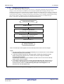
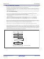
How to Use This Manual
1.
Purpose and Target Readers
This manual is designed to provide the user with an understanding of the hardware functions and electrical
characteristics of the MCU. It is intended for users designing application systems incorporating the MCU. A basic
knowledge of electric circuits, logical circuits, and MCUs is necessary in order to use this manual.
The manual comprises an overview of the product; descriptions of the CPU, system control functions, peripheral
functions, and electrical characteristics; and usage notes.
Particular attention should be paid to the precautionary notes when using the manual. These notes occur
within the body of the text, at the end of each section, and in the Usage Notes section.
The revision history summarizes the locations of revisions and additions. It does not list all revisions. Refer
to the text of the manual for details.
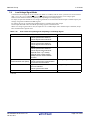
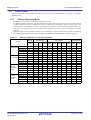
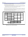
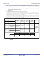
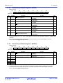
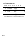
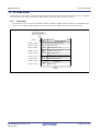
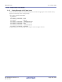
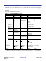
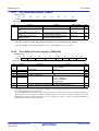
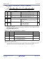
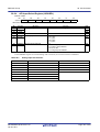
The following documents apply to the R8C/3NT Group. Make sure to refer to the latest versions of these documents.
The newest versions of the documents listed may be obtained from the Renesas Electronics Web site.
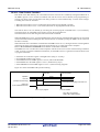
Document Type
Datasheet
Description
Hardware overview and electrical characteristics
User’s manual:
Hardware
Hardware specifications (pin assignments, memory
maps, peripheral function specifications, electrical
characteristics, timing charts) and operation description
Note: Refer to the application notes for details on using
peripheral functions.
Description of CPU instruction set
User’s manual:
Software
Application note
Renesas technical
update
Information on using peripheral functions and
application examples
Sample programs
Information on writing programs in assembly language
and C
Product specifications, updates on documents, etc.
Document Title
R8C/3NT Group
Datasheet
R8C/3NT Group
User’s Manual:
Hardware
Document No.
REJ03B0316
This User’s
manual
R8C/Tiny Series
REJ09B0001
Software Manual
Available from Renesas Electronics
Web site.
2.
Notation of Numbers and Symbols
The notation conventions for register names, bit names, numbers, and symbols used in this manual are described
below.
(1) Register Names, Bit Names, and Pin Names
Registers, bits, and pins are referred to in the text by symbols. The symbol is accompanied by the word “register,”
“bit,” or “pin” to distinguish the three categories.
Examples
the PM03 bit in the PM0 register
P3_5 pin, VCC pin
(2) Notation of Numbers
The indication “b” is appended to numeric values given in binary format. However, nothing is appended to the
values of single bits. The indication “h” is appended to numeric values given in hexadecimal format. Nothing is
appended to numeric values given in decimal format.
Examples
Binary: 11b
Hexadecimal: EFA0h
Decimal: 1234
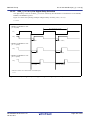
3.
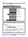
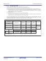
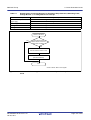
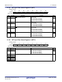
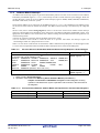
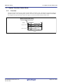
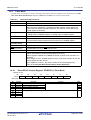
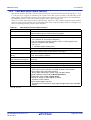
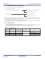
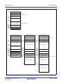
Register Notation
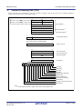
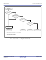
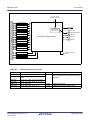
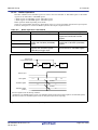
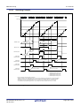
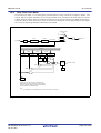
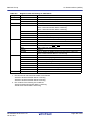
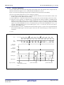
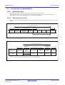
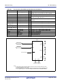
The symbols and terms used in register diagrams are described below.
x.x.x
XXX Register (Symbol)
Address XXXXh
Bit
b7
Symbol XXX7
After Reset
0
Bit
b0
b1
b2
b3
b4
b5
b6
b7
b6
XXX6
0
Symbol
XXX0 XXX bit
XXX1
—
—
XXX4
XXX5
XXX6
XXX7
b5
XXX5
0
b4
XXX4
0
b3
—
0
Bit Name
b2
—
0
b1
XXX1
0
b0
XXX0
0
Function
b1 b0
0 0: XXX
0 1: XXX
1 0: Do not set.
1 1: XXX
Nothing is assigned. If necessary, set to 0. When read, the content is undefined.
Reserved bit
Set to 0.
XXX bit
Function varies according to the operating mode.
XXX bit
0: XXX
1: XXX
*2
*1
R/W
R/W
R/W
—
R/W
R/W
W
R/W
R
*3
*1
R/W: Read and write.
R: Read only.
W: Write only.
—: Nothing is assigned.
*2
• Reserved bit
Reserved bit. Set to specified value.
*3
• Nothing is assigned.
Nothing is assigned to the bit. As the bit may be used for future functions, if necessary, set to 0.
• Do not set to a value.
Operation is not guaranteed when a value is set.
• Function varies according to the operating mode.
The function of the bit varies with the peripheral function mode. Refer to the register diagram for information
on the individual modes.
4.
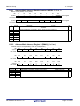
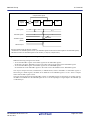
List of Abbreviations and Acronyms
Abbreviation
ACIA
bps
CRC
DMA
DMAC
GSM
Hi-Z
IEBus
I/O
IrDA
LSB
MSB
NC
PLL
PWM
SIM
UART
VCO
Full Form
Asynchronous Communication Interface Adapter
bits per second
Cyclic Redundancy Check
Direct Memory Access
Direct Memory Access Controller
Global System for Mobile Communications
High Impedance
Inter Equipment Bus
Input/Output
Infrared Data Association
Least Significant Bit
Most Significant Bit
Non-Connection
Phase Locked Loop
Pulse Width Modulation
Subscriber Identity Module
Universal Asynchronous Receiver/Transmitter
Voltage Controlled Oscillator
All trademarks and registered trademarks are the property of their respective owners.
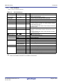
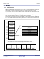
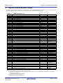
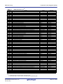
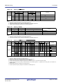
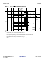
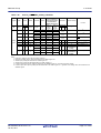
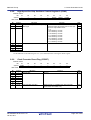
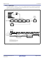
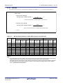
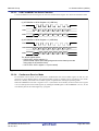
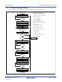
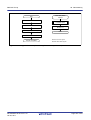
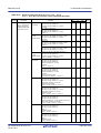
Table of Contents
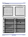
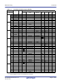
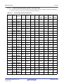
SFR Page Reference ........................................................................................................................... B - 1
1.
Overview ......................................................................................................................................... 1
1.1
1.1.1
1.1.2
1.2
1.3
1.4
1.5
2.
Features .....................................................................................................................................................
Applications ..........................................................................................................................................
Specifications ........................................................................................................................................
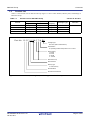
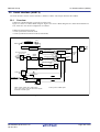
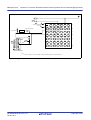
Product List ...............................................................................................................................................
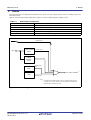
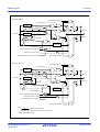
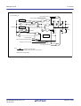
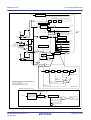
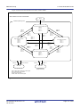
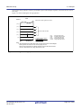
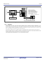
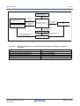
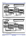
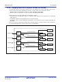
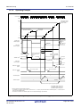
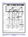
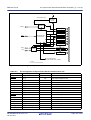
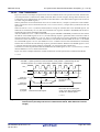
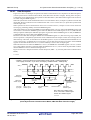
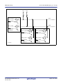
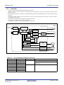
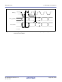
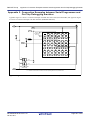
Block Diagram ..........................................................................................................................................
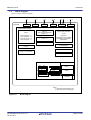
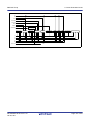
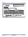
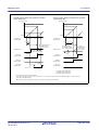
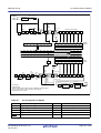
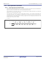
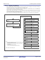
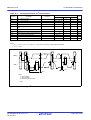
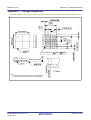
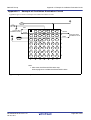
Pin Assignment ..........................................................................................................................................
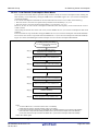
Pin Functions .............................................................................................................................................
1
1
2
4
5
6
8
Central Processing Unit (CPU) ..................................................................................................... 10
2.1
2.2
2.3
2.4
2.5
2.6
2.7
2.8
2.8.1
2.8.2
2.8.3
2.8.4
2.8.5
2.8.6
2.8.7
2.8.8
2.8.9
2.8.10
3.
Data Registers (R0, R1, R2, and R3) ......................................................................................................
Address Registers (A0 and A1) ...............................................................................................................
Frame Base Register (FB) .......................................................................................................................
Interrupt Table Register (INTB) ..............................................................................................................
Program Counter (PC) .............................................................................................................................
User Stack Pointer (USP) and Interrupt Stack Pointer (ISP) ..................................................................
Static Base Register (SB) ........................................................................................................................
Flag Register (FLG) ................................................................................................................................
Carry Flag (C) .....................................................................................................................................
Debug Flag (D) ...................................................................................................................................
Zero Flag (Z) .......................................................................................................................................
Sign Flag (S) .......................................................................................................................................
Register Bank Select Flag (B) ............................................................................................................
Overflow Flag (O) ..............................................................................................................................
Interrupt Enable Flag (I) .....................................................................................................................
Stack Pointer Select Flag (U) ..............................................................................................................
Processor Interrupt Priority Level (IPL) .............................................................................................
Reserved Bit ........................................................................................................................................
11
11
11
11
11
11
11
11
11
11
11
11
11
11
12
12
12
12
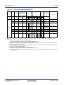
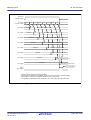
Memory ......................................................................................................................................... 13
3.1
R8C/3NT Group ...................................................................................................................................... 13
4.
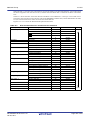
Special Function Registers (SFRs) ............................................................................................... 14
5.
Resets ........................................................................................................................................... 29
5.1
5.1.1
5.1.2
5.1.3
5.1.4
5.2
5.2.1
5.2.2
5.3
5.4
5.5
5.6
Registers ..................................................................................................................................................
Processor Mode Register 0 (PM0) ......................................................................................................
Reset Source Determination Register (RSTFR) .................................................................................
Option Function Select Register (OFS) ..............................................................................................
Option Function Select Register 2 (OFS2) .........................................................................................
Hardware Reset .......................................................................................................................................
When Power Supply is Stable .............................................................................................................
Power On ............................................................................................................................................
Power-On Reset Function .......................................................................................................................
Voltage Monitor 0 Reset .........................................................................................................................
Watchdog Timer Reset ............................................................................................................................
Software Reset .........................................................................................................................................
A-1
31
31
31
32
33
34
34
34
36
37
38
38
5.7
5.8
6.
Cold Start-Up/Warm Start-Up Determination Function ......................................................................... 39
Reset Source Determination Function ..................................................................................................... 39
Voltage Detection Circuit .............................................................................................................. 40
6.1
6.2
6.2.1
6.2.2
6.2.3
6.2.4
6.2.5
6.2.6
6.2.7
6.2.8
6.2.9
6.3
6.3.1
6.3.2
6.3.3
6.4
6.5
6.6
7.
Overview .................................................................................................................................................
Registers ..................................................................................................................................................
Voltage Monitor Circuit Control Register (CMPA) ...........................................................................
Voltage Monitor Circuit Edge Select Register (VCAC) ....................................................................
Voltage Detect Register 1 (VCA1) .....................................................................................................
Voltage Detect Register 2 (VCA2) .....................................................................................................
Voltage Detection 1 Level Select Register (VD1LS) .........................................................................
Voltage Monitor 0 Circuit Control Register (VW0C) ........................................................................
Voltage Monitor 1 Circuit Control Register (VW1C) ........................................................................
Voltage Monitor 2 Circuit Control Register (VW2C) ........................................................................
Option Function Select Register (OFS) ..............................................................................................
VCC Input Voltage ..................................................................................................................................
Monitoring Vdet0 ...............................................................................................................................
Monitoring Vdet1 ...............................................................................................................................
Monitoring Vdet2 ...............................................................................................................................
Voltage Monitor 0 Reset .........................................................................................................................
Voltage Monitor 1 Interrupt ....................................................................................................................
Voltage Monitor 2 Interrupt ....................................................................................................................
40
44
44
45
45
46
47
48
49
50
51
52
52
52
52
53
54
56
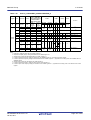
I/O Ports ........................................................................................................................................ 58
7.1
7.2
7.3
7.4
7.4.1
7.4.2
7.4.3
7.4.4
7.4.5
7.4.6
7.4.7
7.4.8
7.4.9
7.4.10
7.4.11
7.4.12
7.4.13
7.4.14
7.4.15
7.4.16
7.4.17
7.4.18
7.4.19
7.4.20
7.4.21
Functions of I/O Ports .............................................................................................................................
Effect on Peripheral Functions ................................................................................................................
Pins Other than I/O Ports .........................................................................................................................
Registers ..................................................................................................................................................
Port Pi Direction Register (PDi) (i = 0 to 4, 6) ...................................................................................
Port Pi Register (Pi) (i = 0 to 4, 6) ......................................................................................................
Timer RA Pin Select Register (TRASR) ............................................................................................
Timer RB/RC Pin Select Register (TRBRCSR) .................................................................................
Timer RC Pin Select Register 0 (TRCPSR0) .....................................................................................
Timer RC Pin Select Register 1 (TRCPSR1) .....................................................................................
Timer Pin Select Register (TIMSR) ...................................................................................................
UART0 Pin Select Register (U0SR) ...................................................................................................
UART1 Pin Select Register (U1SR) ...................................................................................................
UART2 Pin Select Register 0 (U2SR0) ..............................................................................................
UART2 Pin Select Register 1 (U2SR1) ..............................................................................................
SSU/IIC Pin Select Register (SSUIICSR) ..........................................................................................
Low-Voltage Signal Mode Control Register 1 (LVMR1) ..................................................................
INT Interrupt Input Pin Select Register (INTSR) ...............................................................................
I/O Function Pin Select Register (PINSR) .........................................................................................
Low-Voltage Signal Mode Control Register (LVMR) .......................................................................
Pull-Up Control Register 0 (PUR0) ....................................................................................................
Pull-Up Control Register 1 (PUR1) ....................................................................................................
Port P1 Drive Capacity Control Register (P1DRR) ............................................................................
Port P2 Drive Capacity Control Register (P2DRR) ............................................................................
Drive Capacity Control Register 0 (DRR0) ........................................................................................
A-2
58
59
59
74
74
75
76
76
77
78
78
79
79
80
80
81
81
82
83
84
85
85
86
86
87
7.4.22 Drive Capacity Control Register 1 (DRR1) ........................................................................................ 88
7.4.23 Input Threshold Control Register 0 (VLT0) ....................................................................................... 89
7.4.24 Input Threshold Control Register 1 (VLT1) ....................................................................................... 89
7.5
Port Settings ............................................................................................................................................ 90
7.6
Low-Voltage Signal Mode .................................................................................................................... 116
7.7
Unassigned Pin Handling ...................................................................................................................... 117
8.
Bus .............................................................................................................................................. 118
9.
Clock Generation Circuit ............................................................................................................. 120
9.1
9.2
9.2.1
9.2.2
9.2.3
9.2.4
9.2.5
9.2.6
9.2.7
9.2.8
9.2.9
9.2.10
9.2.11
9.2.12
9.2.13
9.2.14
9.2.15
9.3
9.4
9.4.1
9.4.2
9.5
9.6
9.6.1
9.6.2
9.6.3
9.6.4
9.6.5
9.6.6
9.6.7
9.6.8
9.6.9
9.6.10
9.7
9.7.1
9.7.2
9.7.3
9.8
9.8.1
Overview ...............................................................................................................................................
Registers ................................................................................................................................................
System Clock Control Register 0 (CM0) ..........................................................................................
System Clock Control Register 1 (CM1) ..........................................................................................
System Clock Control Register 3 (CM3) ..........................................................................................
Oscillation Stop Detection Register (OCD) ......................................................................................
High-Speed On-Chip Oscillator Control Register 7 (FRA7) ............................................................
High-Speed On-Chip Oscillator Control Register 0 (FRA0) ............................................................
High-Speed On-Chip Oscillator Control Register 1 (FRA1) ............................................................
High-Speed On-Chip Oscillator Control Register 2 (FRA2) ............................................................
Clock Prescaler Reset Flag (CPSRF) ................................................................................................
High-Speed On-Chip Oscillator Control Register 4 (FRA4) ............................................................
High-Speed On-Chip Oscillator Control Register 5 (FRA5) ............................................................
High-Speed On-Chip Oscillator Control Register 6 (FRA6) ............................................................
High-Speed On-Chip Oscillator Control Register 3 (FRA3) ............................................................
Voltage Detect Register 2 (VCA2) ...................................................................................................
I/O Function Pin Select Register (PINSR) .......................................................................................
XIN Clock .............................................................................................................................................
On-Chip Oscillator Clock ......................................................................................................................
Low-Speed On-Chip Oscillator Clock ..............................................................................................
High-Speed On-Chip Oscillator Clock .............................................................................................
XCIN Clock ...........................................................................................................................................
CPU Clock and Peripheral Function Clock ...........................................................................................
System Clock ....................................................................................................................................
CPU Clock ........................................................................................................................................
Peripheral Function Clock (f1, f2, f4, f8, and f32) ...........................................................................
fOCO .................................................................................................................................................
fOCO40M .........................................................................................................................................
fOCO-F .............................................................................................................................................
fOCO-S .............................................................................................................................................
fOCO128 ...........................................................................................................................................
fC, fC2, fC4, and fC32 ......................................................................................................................
fOCO-WDT ......................................................................................................................................
Power Control ........................................................................................................................................
Standard Operating Mode .................................................................................................................
Wait Mode ........................................................................................................................................
Stop Mode .........................................................................................................................................
Oscillation Stop Detection Function .....................................................................................................
How to Use Oscillation Stop Detection Function .............................................................................
A-3
120
123
123
124
125
127
127
128
128
129
129
130
130
130
130
131
132
134
135
135
135
136
137
137
137
137
137
137
137
138
138
138
138
139
139
141
145
148
148
9.9
Notes on Clock Generation Circuit ....................................................................................................... 151
9.9.1
Stop Mode ......................................................................................................................................... 151
9.9.2
Wait Mode ........................................................................................................................................ 151
9.9.3
Oscillation Stop Detection Function ................................................................................................. 152
9.9.4
Oscillation Circuit Constants ............................................................................................................ 152
10.
Protection .................................................................................................................................... 153
10.1
Register .................................................................................................................................................. 153
10.1.1 Protect Register (PRCR) ................................................................................................................... 153
11.
Interrupts ..................................................................................................................................... 154
11.1
Overview ............................................................................................................................................... 154
11.1.1 Types of Interrupts ............................................................................................................................ 154
11.1.2 Software Interrupts ........................................................................................................................... 155
11.1.3 Special Interrupts .............................................................................................................................. 156
11.1.4 Peripheral Function Interrupts .......................................................................................................... 156
11.1.5 Interrupts and Interrupt Vectors ........................................................................................................ 157
11.2
Registers ................................................................................................................................................ 160
11.2.1 Interrupt Control Register (TREIC, S2TIC, S2RIC, KUPIC, ADIC, S0TIC, S0RIC, S1TIC, S1RIC,
TRAIC, TRBIC, VCMP1IC, VCMP2IC) ......................................................................................... 160
11.2.2 Interrupt Control Register (FMRDYIC, TRCIC, SCUIC, SSUiIC/IICiIC (i = 0 to 3)) ................... 161
11.2.3 INTi Interrupt Control Register (INTiIC) (i = 0 to 4) ....................................................................... 162
11.3
Interrupt Control .................................................................................................................................... 163
11.3.1 I Flag ................................................................................................................................................. 163
11.3.2 IR Bit ................................................................................................................................................. 163
11.3.3 Bits ILVL2 to ILVL0, IPL ................................................................................................................ 163
11.3.4 Interrupt Sequence ............................................................................................................................ 164
11.3.5 Interrupt Response Time ................................................................................................................... 165
11.3.6 IPL Change when Interrupt Request is Acknowledged .................................................................... 165
11.3.7 Saving Registers ............................................................................................................................... 166
11.3.8 Returning from Interrupt Routine ..................................................................................................... 168
11.3.9 Interrupt Priority ............................................................................................................................... 168
11.3.10 Interrupt Priority Level Selection Circuit ......................................................................................... 169
11.4
INT Interrupt ......................................................................................................................................... 170
11.4.1 INTi Interrupt (i = 0 to 4) .................................................................................................................. 170
11.4.2 INT Interrupt Input Pin Select Register (INTSR) ............................................................................. 170
11.4.3 External Input Enable Register 0 (INTEN) ...................................................................................... 171
11.4.4 External Input Enable Register 1 (INTEN1) .................................................................................... 171
11.4.5 INT Input Filter Select Register 0 (INTF) ........................................................................................ 172
11.4.6 INT Input Filter Select Register 1 (INTF1) ...................................................................................... 172
11.4.7 INTi Input Filter (i = 0 to 4) ............................................................................................................. 173
11.5
Key Input Interrupt ................................................................................................................................ 174
11.5.1 Key Input Enable Register 0 (KIEN) ................................................................................................ 175
11.6
Address Match Interrupt ........................................................................................................................ 176
11.6.1 Address Match Interrupt Enable Register i (AIERi) (i = 0 or 1) ...................................................... 177
11.6.2 Address Match Interrupt Register i (RMADi) (i = 0 or 1) ................................................................ 177
11.7
Timer RC Interrupt, Synchronous Serial Communication Unit Interrupt, I2C bus Interface Interrupt, Flash
Memory Interrupt (Interrupts with Multiple Interrupt Request Sources), and Sensor Control Unit Interrupt
(Interrupt with Single Interrupt Request Sources) ................................................................................ 178
A-4
11.8
Notes on Interrupts ................................................................................................................................
11.8.1 Reading Address 00000h ..................................................................................................................
11.8.2 SP Setting ..........................................................................................................................................
11.8.3 External Interrupt and Key Input Interrupt .......................................................................................
11.8.4 Changing Interrupt Sources ..............................................................................................................
11.8.5 Rewriting Interrupt Control Register ................................................................................................
12.
ID Code Areas ............................................................................................................................ 183
12.1
12.2
12.3
12.4
12.5
12.5.1
13.
180
180
180
180
181
182
Overview ...............................................................................................................................................
Functions ...............................................................................................................................................
Forced Erase Function ...........................................................................................................................
Standard Serial I/O Mode Disabled Function .......................................................................................
Notes on ID Code Areas ........................................................................................................................
Setting Example of ID Code Areas ...................................................................................................
183
184
185
185
186
186
Option Function Select Area ....................................................................................................... 187
13.1
Overview ............................................................................................................................................... 187
13.2
Registers ................................................................................................................................................ 188
13.2.1 Option Function Select Register (OFS) ............................................................................................ 188
13.2.2 Option Function Select Register 2 (OFS2) ....................................................................................... 189
13.3
Notes on Option Function Select Area .................................................................................................. 190
13.3.1 Setting Example of Option Function Select Area ............................................................................. 190
14.
Watchdog Timer ......................................................................................................................... 191
14.1
Overview ............................................................................................................................................... 191
14.2
Registers ................................................................................................................................................ 193
14.2.1 Processor Mode Register 1 (PM1) .................................................................................................... 193
14.2.2 Watchdog Timer Reset Register (WDTR) ........................................................................................ 193
14.2.3 Watchdog Timer Start Register (WDTS) ......................................................................................... 193
14.2.4 Watchdog Timer Control Register (WDTC) .................................................................................... 194
14.2.5 Count Source Protection Mode Register (CSPR) ............................................................................. 194
14.2.6 Option Function Select Register (OFS) ............................................................................................ 195
14.2.7 Option Function Select Register 2 (OFS2) ....................................................................................... 196
14.3
Functional Description ......................................................................................................................... 197
14.3.1 Common Items for Multiple Modes ................................................................................................. 197
14.3.2 Count Source Protection Mode Disabled .......................................................................................... 198
14.3.3 Count Source Protection Mode Enabled ........................................................................................... 199
15.
DTC ............................................................................................................................................ 200
15.1
Overview ............................................................................................................................................... 200
15.2
Registers ................................................................................................................................................ 201
15.2.1 DTC Control Register j (DTCCRj) (j = 0 to 23) ............................................................................... 202
15.2.2 DTC Block Size Register j (DTBLSj) (j = 0 to 23) .......................................................................... 202
15.2.3 DTC Transfer Count Register j (DTCCTj) (j = 0 to 23) ................................................................... 202
15.2.4 DTC Transfer Count Reload Register j (DTRLDj) (j = 0 to 23) ...................................................... 203
15.2.5 DTC Source Address Register j (DTSARj) (j = 0 to 23) .................................................................. 203
15.2.6 DTC Destination Address Register j (DTDARj) (j = 0 to 23) .......................................................... 203
15.2.7 DTC Activation Enable Register i (DTCENi) (i = 0 to 6) ................................................................ 204
15.2.8 DTC Activation Control Register (DTCTL) .................................................................................... 205
A-5
15.3
Function Description .............................................................................................................................
15.3.1 Overview ...........................................................................................................................................
15.3.2 Activation Sources ............................................................................................................................
15.3.3 Control Data Allocation and DTC Vector Table ..............................................................................
15.3.4 Normal Mode ....................................................................................................................................
15.3.5 Repeat Mode .....................................................................................................................................
15.3.6 Chain Transfers .................................................................................................................................
15.3.7 Interrupt Sources ...............................................................................................................................
15.3.8 Operation Timings ............................................................................................................................
15.3.9 Number of DTC Execution Cycles ...................................................................................................
15.3.10 DTC Activation Source Acknowledgement and Interrupt Source Flags ..........................................
15.4
Notes on DTC ........................................................................................................................................
15.4.1 DTC activation source ......................................................................................................................
15.4.2 DTCENi (i = 0 to 6) Registers ..........................................................................................................
15.4.3 Peripheral Modules ...........................................................................................................................
15.4.4 Interrupt Request ...............................................................................................................................
206
206
206
208
213
214
215
215
216
217
218
220
220
220
220
220
16.
General Overview of Timers ....................................................................................................... 221
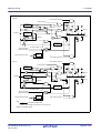
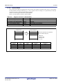
17.
Timer RA ..................................................................................................................................... 222
17.1
17.2
17.2.1
17.2.2
17.2.3
17.2.4
17.2.5
17.2.6
17.3
17.3.1
17.3.2
17.4
17.4.1
17.5
17.5.1
17.6
17.6.1
17.6.2
17.7
17.7.1
17.7.2
17.8
18.
Overview ...............................................................................................................................................
Registers ................................................................................................................................................
Timer RA Control Register (TRACR) ..............................................................................................
Timer RA I/O Control Register (TRAIOC) ......................................................................................
Timer RA Mode Register (TRAMR) ................................................................................................
Timer RA Prescaler Register (TRAPRE) .........................................................................................
Timer RA Register (TRA) ................................................................................................................
Timer RA Pin Select Register (TRASR) ..........................................................................................
Timer Mode ...........................................................................................................................................
Timer RA I/O Control Register (TRAIOC) in Timer Mode ............................................................
Timer Write Control during Count Operation ..................................................................................
Pulse Output Mode ................................................................................................................................
Timer RA I/O Control Register (TRAIOC) in Pulse Output Mode .................................................
Event Counter Mode .............................................................................................................................
Timer RA I/O Control Register (TRAIOC) in Event Counter Mode ...............................................
Pulse Width Measurement Mode ..........................................................................................................
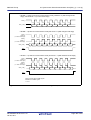
Timer RA I/O Control Register (TRAIOC) in Pulse Width Measurement Mode ............................
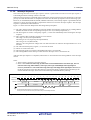
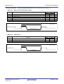
Operating Example ...........................................................................................................................
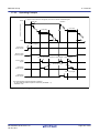
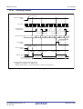
Pulse Period Measurement Mode ..........................................................................................................
Timer RA I/O Control Register (TRAIOC) in Pulse Period Measurement Mode ...........................
Operating Example ...........................................................................................................................
Notes on Timer RA ...............................................................................................................................
222
223
223
223
224
224
225
225
226
226
227
228
229
230
231
232
233
234
235
236
237
238
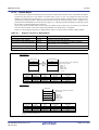
Timer RB ..................................................................................................................................... 239
18.1
Overview ............................................................................................................................................... 239
18.2
Registers ................................................................................................................................................ 240
18.2.1 Timer RB Control Register (TRBCR) .............................................................................................. 240
18.2.2 Timer RB One-Shot Control Register (TRBOCR) ........................................................................... 240
18.2.3 Timer RB I/O Control Register (TRBIOC) ...................................................................................... 241
A-6
18.2.4
18.2.5
18.2.6
18.2.7
18.2.8
18.3
18.3.1
18.3.2
18.4
18.4.1
18.4.2
18.5
18.5.1
18.5.2
18.5.3
18.6
18.6.1
18.6.2
18.7
18.7.1
18.7.2
18.7.3
18.7.4
19.
Timer RB Mode Register (TRBMR) ................................................................................................
Timer RB Prescaler Register (TRBPRE) ..........................................................................................
Timer RB Secondary Register (TRBSC) ..........................................................................................
Timer RB Primary Register (TRBPR) ..............................................................................................
Timer RB/RC Pin Select Register (TRBRCSR) ...............................................................................
Timer Mode ...........................................................................................................................................
Timer RB I/O Control Register (TRBIOC) in Timer Mode .............................................................
Timer Write Control during Count Operation ..................................................................................
Programmable Waveform Generation Mode ........................................................................................
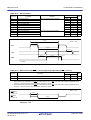
Timer RB I/O Control Register (TRBIOC) in Programmable Waveform Generation Mode ..........
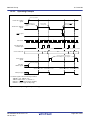
Operating Example ...........................................................................................................................
Programmable One-shot Generation Mode ...........................................................................................
Timer RB I/O Control Register (TRBIOC) in Programmable One-Shot Generation Mode ............
Operating Example ...........................................................................................................................
One-Shot Trigger Selection ..............................................................................................................
Programmable Wait One-Shot Generation Mode .................................................................................
Timer RB I/O Control Register (TRBIOC) in Programmable Wait One-Shot Generation Mode ...
Operating Example ...........................................................................................................................
Notes on Timer RB ................................................................................................................................
Timer Mode ......................................................................................................................................
Programmable Waveform Generation Mode ....................................................................................
Programmable One-shot Generation Mode ......................................................................................
Programmable Wait One-shot Generation Mode .............................................................................
241
242
242
243
243
244
244
245
247
248
249
250
251
252
253
254
255
256
257
257
257
258
258
Timer RC .................................................................................................................................... 259
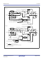
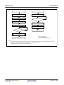
19.1
Overview ...............................................................................................................................................
19.2
Registers ................................................................................................................................................
19.2.1 Module Standby Control Register (MSTCR) ...................................................................................
19.2.2 Timer RC Mode Register (TRCMR) ................................................................................................
19.2.3 Timer RC Control Register 1 (TRCCR1) .........................................................................................
19.2.4 Timer RC Interrupt Enable Register (TRCIER) ...............................................................................
19.2.5 Timer RC Status Register (TRCSR) .................................................................................................
19.2.6 Timer RC I/O Control Register 0 (TRCIOR0) .................................................................................
19.2.7 Timer RC I/O Control Register 1 (TRCIOR1) .................................................................................
19.2.8 Timer RC Counter (TRC) .................................................................................................................
19.2.9 Timer RC General Registers A, B, C, and D (TRCGRA, TRCGRB, TRCGRC, TRCGRD) ..........
19.2.10 Timer RC Control Register 2 (TRCCR2) .........................................................................................
19.2.11 Timer RC Digital Filter Function Select Register (TRCDF) ............................................................
19.2.12 Timer RC Output Master Enable Register (TRCOER) ....................................................................
19.2.13 Timer RC Trigger Control Register (TRCADCR) ...........................................................................
19.2.14 Timer RB/RC Pin Select Register (TRBRCSR) ...............................................................................
19.2.15 Timer RC Pin Select Register 0 (TRCPSR0) ...................................................................................
19.2.16 Timer RC Pin Select Register 1 (TRCPSR1) ...................................................................................
19.3
Common Items for Multiple Modes ......................................................................................................
19.3.1 Count Source .....................................................................................................................................
19.3.2 Buffer Operation ...............................................................................................................................
19.3.3 Digital Filter ......................................................................................................................................
19.3.4 Forced Cutoff of Pulse Output ..........................................................................................................
19.4
Timer Mode (Input Capture Function) ..................................................................................................
A-7
259
261
262
263
264
264
265
266
266
267
267
268
268
269
269
270
270
271
272
272
273
275
276
278
19.4.1
19.4.2
19.4.3
19.5
19.5.1
19.5.2
19.5.3
19.5.4
19.5.5
19.5.6
19.6
19.6.1
19.6.2
19.6.3
19.7
19.7.1
19.7.2
19.7.3
19.7.4
19.8
19.9
19.9.1
19.9.2
19.9.3
19.9.4
19.9.5
19.9.6
19.9.7
20.
Timer RC I/O Control Register 0 (TRCIOR0) for Input Capture Function .....................................
Timer RC I/O Control Register 1 (TRCIOR1) for Input Capture Function .....................................
Operating Example ...........................................................................................................................
Timer Mode (Output Compare Function) .............................................................................................
Timer RC Control Register 1 (TRCCR1) for Output Compare Function ........................................
Timer RC I/O Control Register 0 (TRCIOR0) for Output Compare Function ................................
Timer RC I/O Control Register 1 (TRCIOR1) for Output Compare Function ................................
Timer RC Control Register 2 (TRCCR2) for Output Compare Function ........................................
Operating Example ...........................................................................................................................
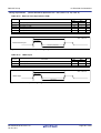
Changing Output Pins in Registers TRCGRC and TRCGRD ..........................................................
PWM Mode ...........................................................................................................................................
Timer RC Control Register 1 (TRCCR1) in PWM Mode ................................................................
Timer RC Control Register 2 (TRCCR2) in PWM Mode ................................................................
Operating Example ...........................................................................................................................
PWM2 Mode .........................................................................................................................................
Timer RC Control Register 1 (TRCCR1) in PWM2 Mode ..............................................................
Timer RC Control Register 2 (TRCCR2) in PWM2 Mode ..............................................................
Timer RC Digital Filter Function Select Register (TRCDF) in PWM2 Mode .................................
Operating Example ...........................................................................................................................
Timer RC Interrupt ................................................................................................................................
Notes on Timer RC ................................................................................................................................
TRC Register ....................................................................................................................................
TRCSR Register ..............................................................................................................................
TRCCR1 Register .............................................................................................................................
Count Source Switching ...................................................................................................................
Input Capture Function .....................................................................................................................
TRCMR Register in PWM2 Mode ...................................................................................................
Count Source fOCO40M ..................................................................................................................
280
281
282
283
285
286
287
288
289
290
292
294
295
296
298
300
301
302
303
306
307
307
307
307
307
308
308
308
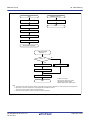
Timer RE ..................................................................................................................................... 309
20.1
Overview ............................................................................................................................................... 309
20.2
Real-Time Clock Mode ......................................................................................................................... 310
20.2.1 Timer RE Second Data Register (TRESEC) in Real-Time Clock Mode ......................................... 312
20.2.2 Timer RE Minute Data Register (TREMIN) in Real-Time Clock Mode ......................................... 312
20.2.3 Timer RE Hour Data Register (TREHR) in Real-Time Clock Mode ............................................... 313
20.2.4 Timer RE Day of Week Data Register (TREWK) in Real-Time Clock Mode ................................ 313
20.2.5 Timer RE Control Register 1 (TRECR1) in Real-Time Clock Mode .............................................. 314
20.2.6 Timer RE Control Register 2 (TRECR2) in Real-Time Clock Mode .............................................. 315
20.2.7 Timer RE Count Source Select Register (TRECSR) in Real-Time Clock Mode ............................. 316
20.2.8 Timer Pin Select Register (TIMSR) ................................................................................................. 316
20.2.9 Operating Example ........................................................................................................................... 317
20.3
Output Compare Mode .......................................................................................................................... 318
20.3.1 Timer RE Counter Data Register (TRESEC) in Output Compare Mode ......................................... 320
20.3.2 Timer RE Compare Data Register (TREMIN) in Output Compare Mode ....................................... 320
20.3.3 Timer RE Control Register 1 (TRECR1) in Output Compare Mode ............................................... 321
20.3.4 Timer RE Control Register 2 (TRECR2) in Output Compare Mode ............................................... 321
20.3.5 Timer RE Count Source Select Register (TRECSR) in Output Compare Mode .............................. 322
20.3.6 Timer Pin Select Register (TIMSR) ................................................................................................. 322
20.3.7 Operating Example ........................................................................................................................... 323
A-8
20.4
Notes on Timer RE ................................................................................................................................
20.4.1 Starting and Stopping Count .............................................................................................................
20.4.2 Register Setting .................................................................................................................................
20.4.3 Time Reading Procedure of Real-Time Clock Mode .......................................................................
21.
Serial Interface (UARTi (i = 0 or 1)) ............................................................................................ 327
21.1
21.2
21.2.1
21.2.2
21.2.3
21.2.4
21.2.5
21.2.6
21.2.7
21.2.8
21.2.9
21.3
21.3.1
21.3.2
21.3.3
21.3.4
21.4
21.4.1
21.4.2
21.5
22.
324
324
324
326
Overview ...............................................................................................................................................
Registers ................................................................................................................................................
UARTi Transmit/Receive Mode Register (UiMR) (i = 0 or 1) ........................................................
UARTi Bit Rate Register (UiBRG) (i = 0 or 1) ................................................................................
UARTi Transmit Buffer Register (UiTB) (i = 0 or 1) ......................................................................
UARTi Transmit/Receive Control Register 0 (UiC0) (i = 0 or 1) ....................................................
UARTi Transmit/Receive Control Register 1 (UiC1) (i = 0 or 1) ....................................................
UARTi Receive Buffer Register (UiRB) (i = 0 or 1) .......................................................................
UART0 Pin Select Register (U0SR) .................................................................................................
UART1 Pin Select Register (U1SR) .................................................................................................
Low-Voltage Signal Mode Control Register (LVMR) .....................................................................
Clock Synchronous Serial I/O Mode .....................................................................................................
Measure for Dealing with Communication Errors ...........................................................................
Polarity Select Function ....................................................................................................................
LSB First/MSB First Select Function ...............................................................................................
Continuous Receive Mode ................................................................................................................
Clock Asynchronous Serial I/O (UART) Mode ....................................................................................
Bit Rate .............................................................................................................................................
Measure for Dealing with Communication Errors ...........................................................................
Notes on Serial Interface (UARTi (i = 0 or 1)) .....................................................................................
327
329
329
329
330
331
331
332
333
333
334
335
339
340
340
341
342
347
348
349
Serial Interface (UART2) ............................................................................................................ 350
22.1
Overview ...............................................................................................................................................
22.2
Registers ................................................................................................................................................
22.2.1 UART2 Transmit/Receive Mode Register (U2MR) .........................................................................
22.2.2 UART2 Bit Rate Register (U2BRG) ................................................................................................
22.2.3 UART2 Transmit Buffer Register (U2TB) .......................................................................................
22.2.4 UART2 Transmit/Receive Control Register 0 (U2C0) ....................................................................
22.2.5 UART2 Transmit/Receive Control Register 1 (U2C1) ....................................................................
22.2.6 UART2 Receive Buffer Register (U2RB) ........................................................................................
22.2.7 UART2 Digital Filter Function Select Register (URXDF) ..............................................................
22.2.8 UART2 Pin Select Register 0 (U2SR0) ............................................................................................
22.2.9 UART2 Pin Select Register 1 (U2SR1) ............................................................................................
22.2.10 Low-Voltage Signal Mode Control Register (LVMR) .....................................................................
22.3
Clock Synchronous Serial I/O Mode .....................................................................................................
22.3.1 Measure for Dealing with Communication Errors ...........................................................................
22.3.2 CLK Polarity Select Function ...........................................................................................................
22.3.3 LSB First/MSB First Select Function ...............................................................................................
22.3.4 Continuous Receive Mode ................................................................................................................
22.3.5 Serial Data Logic Switching Function ..............................................................................................
22.3.6 CTS/RTS Function ...........................................................................................................................
22.4
Clock Asynchronous Serial I/O (UART) Mode ....................................................................................
22.4.1 Bit Rate .............................................................................................................................................
A-9
350
352
352
352
353
354
355
356
357
357
358
359
360
364
364
365
365
366
366
367
371
22.4.2 Measure for Dealing with Communication Errors ...........................................................................
22.4.3 LSB First/MSB First Select Function ...............................................................................................
22.4.4 Serial Data Logic Switching Function ..............................................................................................
22.4.5 TXD and RXD I/O Polarity Inverse Function ..................................................................................
22.4.6 CTS/RTS Function ...........................................................................................................................
22.4.7 RXD2 Digital Filter Select Function ................................................................................................
22.5
Notes on Serial Interface (UART2) .......................................................................................................
22.5.1 Clock Synchronous Serial I/O Mode ................................................................................................
23.
23.1
24.
Clock Synchronous Serial Interface ............................................................................................ 376
Mode Selection ...................................................................................................................................... 376
Synchronous Serial Communication Unit (SSU_i (i = 0 to 3)) .................................................... 377
24.1
Overview ...............................................................................................................................................
24.2
Registers ................................................................................................................................................
24.2.1 Module Standby Control Register (MSTCR) ...................................................................................
24.2.2 SSU/IIC Pin Select Register (SSUIICSR) ........................................................................................
24.2.3 I/O Function Pin Select Register 2 (PINSR2) ..................................................................................
24.2.4 SSi Bit Counter Register (SSiBR) (i = 0 to 3) ..................................................................................
24.2.5 SSi Transmit Data Register (SSiTDR) (i = 0 to 3) ...........................................................................
24.2.6 SSi Receive Data Register (SSiRDR) (i = 0 to 3) .............................................................................
24.2.7 SSi Control Register H (SSiCRH) (i = 0 to 3) ..................................................................................
24.2.8 SSi Control Register L (SSiCRL) (i = 0 to 3) ...................................................................................
24.2.9 SSi Mode Register (SSiMR) (i = 0 to 3) ...........................................................................................
24.2.10 SSi Enable Register (SSiER) (i = 0 to 3) ..........................................................................................
24.2.11 SSi Status Register (SSiSR) (i = 0 to 3) ............................................................................................
24.2.12 SSi Mode Register 2 (SSiMR2) (i = 0 to 3) ......................................................................................
24.3
Common Items for Multiple Modes ......................................................................................................
24.3.1 Transfer Clock ..................................................................................................................................
24.3.2 SSi Shift Register (SSiTRSR) (i = 0 to 3) ........................................................................................
24.3.3 Interrupt Requests .............................................................................................................................
24.3.4 Communication Modes and Pin Functions .......................................................................................
24.4
Clock Synchronous Communication Mode ..........................................................................................
24.4.1 Initialization in Clock Synchronous Communication Mode ............................................................
24.4.2 Data Transmission ............................................................................................................................
24.4.3 Data Reception ..................................................................................................................................
24.5
Operation in 4-Wire Bus Communication Mode ..................................................................................
24.5.1 Initialization in 4-Wire Bus Communication Mode .........................................................................
24.5.2 Data Transmission ............................................................................................................................
24.5.3 Data Reception ..................................................................................................................................
24.5.4 SCS_i (i = 0 to 3) Pin Control and Arbitration .................................................................................
24.6
Notes on Synchronous Serial Communication Unit ..............................................................................
25.
372
372
373
373
374
374
375
375
377
379
379
380
380
381
381
382
382
383
384
385
386
387
388
388
390
391
392
393
393
394
396
400
401
402
404
406
407
I2C bus Interface (IIC_i (i = 0 to 3)) ............................................................................................. 408
25.1
Overview ............................................................................................................................................... 408
25.2
Registers ................................................................................................................................................ 411
25.2.1 Module Standby Control Register (MSTCR) ................................................................................... 411
25.2.2 SSU/IIC Pin Select Register (SSUIICSR) ........................................................................................ 412
25.2.3 I/O Function Pin Select Register (PINSR) ....................................................................................... 413
A - 10
25.2.4 I/O Function Pin Select Register 1 (PINSR1) .................................................................................. 414
25.2.5 I/O Function Pin Select Register 2 (PINSR2) .................................................................................. 415
25.2.6 IIC_i Transmit Data Register (ICiDRT) (i = 0 to 3) ......................................................................... 416
25.2.7 IIC_i Receive Data Register (ICiDRR) (i = 0 to 3) .......................................................................... 416
25.2.8 IIC_i Control Register 1 (ICiCR1) (i = 0 to 3) ................................................................................. 417
25.2.9 IIC_i Control Register 2 (ICiCR2) (i = 0 to 3) ................................................................................. 418
25.2.10 IIC_i Mode Register (ICiMR) (i = 0 to 3) ........................................................................................ 419
25.2.11 IIC_i Interrupt Enable Register (ICiIER) (i = 0 to 3) ....................................................................... 420
25.2.12 IIC_i Status Register (ICiSR) (i = 0 to 3) ......................................................................................... 421
25.2.13 Slave Address Register i (SARi) (i = 0 to 3) .................................................................................... 422
25.2.14 IIC_i Shift Register i (ICiDRS) (i = 0 to 3) ...................................................................................... 422
25.3
Common Items for Multiple Modes ...................................................................................................... 423
25.3.1 Transfer Clock .................................................................................................................................. 423
25.3.2 SDA_i (i = 0 to 3) Pin Digital Delay Selection ................................................................................ 425
25.3.3 Interrupt Requests ............................................................................................................................. 426
25.4
I2C bus Interface Mode ......................................................................................................................... 427
25.4.1 I2C bus Format .................................................................................................................................. 427
25.4.2 Master Transmit Operation ............................................................................................................... 428
25.4.3 Master Receive Operation ................................................................................................................ 430
25.4.4 Slave Transmit Operation ................................................................................................................. 433
25.4.5 Slave Receive Operation ................................................................................................................... 436
25.5
Clock Synchronous Serial Mode ........................................................................................................... 438
25.5.1 Clock Synchronous Serial Format .................................................................................................... 438
25.5.2 Transmit Operation ........................................................................................................................... 439
25.5.3 Receive Operation ............................................................................................................................. 440
25.6
Examples of Register Setting ................................................................................................................ 441
25.7
Noise Canceller ..................................................................................................................................... 445
25.8
Bit Synchronization Circuit ................................................................................................................... 446
25.9
Notes on I2C bus Interface .................................................................................................................... 447
25.9.1 Master Receive Mode ....................................................................................................................... 447
25.9.2 The ICE Bit in the ICiCR1 (i = 0 to 3) Register and the IICiRST (i = 0 to 3) Bit in the ICiCR2 Register
447
26.
A/D Converter ............................................................................................................................. 449
26.1
Overview ............................................................................................................................................... 449
26.2
Registers ................................................................................................................................................ 451
26.2.1 On-Chip Reference Voltage Control Register (OCVREFCR) ......................................................... 451
26.2.2 A/D Register i (ADi) (i = 0 to 7) ...................................................................................................... 452
26.2.3 A/D Mode Register (ADMOD) ........................................................................................................ 453
26.2.4 A/D Input Select Register (ADINSEL) ............................................................................................ 454
26.2.5 A/D Control Register 0 (ADCON0) ................................................................................................. 455
26.2.6 A/D Control Register 1 (ADCON1) ................................................................................................. 456
26.3
Common Items for Multiple Modes ...................................................................................................... 457
26.3.1 Input/Output Pins .............................................................................................................................. 457
26.3.2 A/D Conversion Cycles .................................................................................................................... 457
26.3.3 A/D Conversion Start Condition ....................................................................................................... 459
26.3.4 A/D Conversion Result ..................................................................................................................... 461
26.3.5 Low Current Consumption Function ................................................................................................ 461
26.3.6 On-Chip Reference Voltage (OCVREF) .......................................................................................... 461
A - 11
26.3.7
26.4
26.5
26.6
26.7
26.8
26.9
26.10
27.
A/D Open-Circuit Detection Assist Function ...................................................................................
One-Shot Mode .....................................................................................................................................
Repeat Mode 0 .......................................................................................................................................
Repeat Mode 1 .......................................................................................................................................
Single Sweep Mode ...............................................................................................................................
Repeat Sweep Mode ..............................................................................................................................
Output Impedance of Sensor under A/D Conversion ............................................................................
Notes on A/D Converter ........................................................................................................................
Sensor Control Unit .................................................................................................................... 473
27.1
Overview ...............................................................................................................................................
27.2
Registers ................................................................................................................................................
27.2.1 SCU Control Register 0 (SCUCR0) .................................................................................................
27.2.2 SCU Mode Register (SCUMR) ........................................................................................................
27.2.3 SCU Timing Control Register 0 (SCTCR0) .....................................................................................
27.2.4 SCU Timing Control Register 1 (SCTCR1) .....................................................................................
27.2.5 SCU Timing Control Register 2 (SCTCR2) .....................................................................................
27.2.6 SCU Timing Control Register 3 (SCTCR3) .....................................................................................
27.2.7 SCU Channel Control Register (SCHCR) ........................................................................................
27.2.8 SCU Channel Control Counter (SCUCHC) ......................................................................................
27.2.9 SCU Flag Register (SCUFR) ............................................................................................................
27.2.10 SCU Status Counter (SCUSTC) .......................................................................................................
27.2.11 SCU Secondary Counter Set Register (SCSCSR) ............................................................................
27.2.12 SCU Secondary Counter (SCUSCC) ................................................................................................
27.2.13 SCU Destination Address Register (SCUDAR) ...............................................................................
27.2.14 SCU Data Buffer Register (SCUDBR) .............................................................................................
27.2.15 SCU Primary Counter (SCUPRC) ....................................................................................................
27.2.16 Touch Sensor Input Enable Register 0 (TSIER0) .............................................................................
27.3
Functional Description ..........................................................................................................................
27.3.1 Common Items for Multiple Modes .................................................................................................
27.3.2 Specifications and Operation Example of Sensor Control Unit .......................................................
27.4
Principle of Measurement Operation ....................................................................................................
27.5
Notes on Sensor Control Unit ...............................................................................................................
27.5.1 A/D Converter ...................................................................................................................................
27.5.2 Address to Store Detection Data .......................................................................................................
27.5.3 Wait Mode ........................................................................................................................................
27.5.4 Measurement Trigger ........................................................................................................................
27.5.5 Charging Time ..................................................................................................................................
28.
461
463
464
465
467
469
471
472
474
475
475
476
476
477
479
481
482
482
483
484
484
484
485
486
487
487
488
488
493
495
498
498
498
498
498
498
Flash Memory ............................................................................................................................. 499
28.1
28.2
28.3
28.3.1
28.3.2
28.3.3
28.4
28.4.1
28.4.2
Overview ...............................................................................................................................................
Memory Map .........................................................................................................................................
Functions to Prevent Flash Memory from being Rewritten ..................................................................
ID Code Check Function ..................................................................................................................
ROM Code Protect Function ............................................................................................................
Option Function Select Register (OFS) ............................................................................................
CPU Rewrite Mode ...............................................................................................................................
Flash Memory Status Register (FST) ...............................................................................................
Flash Memory Control Register 0 (FMR0) ......................................................................................
A - 12
499
500
502
502
503
503
504
505
507
28.4.3 Flash Memory Control Register 1 (FMR1) ......................................................................................
28.4.4 Flash Memory Control Register 2 (FMR2) ......................................................................................
28.4.5 EW0 Mode ........................................................................................................................................
28.4.6 EW1 Mode ........................................................................................................................................
28.4.7 Suspend Operation ............................................................................................................................
28.4.8 How to Set and Exit Each Mode .......................................................................................................
28.4.9 BGO (BackGround Operation) Function ..........................................................................................
28.4.10 Data Protect Function .......................................................................................................................
28.4.11 Software Commands .........................................................................................................................
28.4.12 Full Status Check ..............................................................................................................................
28.5
Standard Serial I/O Mode ......................................................................................................................
28.5.1 ID Code Check Function ..................................................................................................................
28.6
Parallel I/O Mode ..................................................................................................................................
28.6.1 ROM Code Protect Function ............................................................................................................
28.7
Notes on Flash Memory ........................................................................................................................
28.7.1 CPU Rewrite Mode ...........................................................................................................................
29.
510
512
514
514
515
517
518
519
520
529
531
531
534
534
535
535
Reducing Power Consumption ................................................................................................... 539
29.1
Overview ...............................................................................................................................................
29.2
Key Points and Processing Methods for Reducing Power Consumption .............................................
29.2.1 Voltage Detection Circuit .................................................................................................................
29.2.2 Ports ..................................................................................................................................................
29.2.3 Clocks ...............................................................................................................................................
29.2.4 Wait Mode, Stop Mode .....................................................................................................................
29.2.5 Stopping Peripheral Function Clocks ...............................................................................................
29.2.6 Timers ...............................................................................................................................................
29.2.7 A/D Converter ...................................................................................................................................
29.2.8 Clock Synchronous Serial Interface .................................................................................................
29.2.9 Sensor Control Unit ..........................................................................................................................
29.2.10 Reducing Internal Power Consumption ............................................................................................
29.2.11 Stopping Flash Memory ....................................................................................................................
29.2.12 Low-Current-Consumption Read Mode ...........................................................................................
539
539
539
539
539
539
539
539
539
539
540
540
541
542
30.
Electrical Characteristics ............................................................................................................ 543
31.
Usage Notes ............................................................................................................................... 569
31.1
Notes on Clock Generation Circuit ....................................................................................................... 569
31.1.1 Stop Mode ......................................................................................................................................... 569
31.1.2 Wait Mode ........................................................................................................................................ 569
31.1.3 Oscillation Stop Detection Function ................................................................................................. 570
31.1.4 Oscillation Circuit Constants ............................................................................................................ 570
31.2
Notes on Interrupts ................................................................................................................................ 571
31.2.1 Reading Address 00000h .................................................................................................................. 571
31.2.2 SP Setting .......................................................................................................................................... 571
31.2.3 External Interrupt and Key Input Interrupt ....................................................................................... 571
31.2.4 Changing Interrupt Sources .............................................................................................................. 572
31.2.5 Rewriting Interrupt Control Register ................................................................................................ 573
31.3
Notes on ID Code Areas ........................................................................................................................ 574
31.3.1 Setting Example of ID Code Areas ................................................................................................... 574
A - 13
31.4
Notes on Option Function Select Area .................................................................................................. 574
31.4.1 Setting Example of Option Function Select Area ............................................................................. 574
31.5
Notes on DTC ........................................................................................................................................ 575
31.5.1 DTC activation source ...................................................................................................................... 575
31.5.2 DTCENi (i = 0 to 6) Registers .......................................................................................................... 575
31.5.3 Peripheral Modules ........................................................................................................................... 575
31.5.4 Interrupt Request ............................................................................................................................... 575
31.6
Notes on Timer RA ............................................................................................................................... 576
31.7
Notes on Timer RB ................................................................................................................................ 577
31.7.1 Timer Mode ...................................................................................................................................... 577
31.7.2 Programmable Waveform Generation Mode .................................................................................... 577
31.7.3 Programmable One-shot Generation Mode ...................................................................................... 578
31.7.4 Programmable Wait One-shot Generation Mode ............................................................................. 578
31.8
Notes on Timer RC ................................................................................................................................ 579
31.8.1 TRC Register .................................................................................................................................... 579
31.8.2
TRCSR Register .............................................................................................................................. 579
31.8.3 TRCCR1 Register ............................................................................................................................. 579
31.8.4 Count Source Switching ................................................................................................................... 579
31.8.5 Input Capture Function ..................................................................................................................... 580
31.8.6 TRCMR Register in PWM2 Mode ................................................................................................... 580
31.8.7 Count Source fOCO40M .................................................................................................................. 580
31.9
Notes on Timer RE ................................................................................................................................ 581
31.9.1 Starting and Stopping Count ............................................................................................................. 581
31.9.2 Register Setting ................................................................................................................................. 581
31.9.3 Time Reading Procedure of Real-Time Clock Mode ....................................................................... 583
31.10 Notes on Serial Interface (UARTi (i = 0 or 1)) ..................................................................................... 584
31.11 Notes on Serial Interface (UART2) ....................................................................................................... 585
31.11.1 Clock Synchronous Serial I/O Mode ................................................................................................ 585
31.12 Notes on Synchronous Serial Communication Unit .............................................................................. 586
31.13 Notes on I2C bus Interface .................................................................................................................... 586
31.13.1 Master Receive Mode ....................................................................................................................... 586
31.13.2 The ICE Bit in the ICiCR1 (i = 0 to 3) Register and the IICiRST (i = 0 to 3) Bit in the ICiCR2 Register
586
31.14 Notes on A/D Converter ........................................................................................................................ 587
31.15 Notes on Sensor Control Unit ............................................................................................................... 588
31.15.1 A/D Converter ................................................................................................................................... 588
31.15.2 Address to Store Detection Data ....................................................................................................... 588
31.15.3 Wait Mode ........................................................................................................................................ 588
31.15.4 Measurement Trigger ........................................................................................................................ 588
31.15.5 Charging Time .................................................................................................................................. 588
31.16 Notes on Flash Memory ........................................................................................................................ 589
31.16.1 CPU Rewrite Mode ........................................................................................................................... 589
31.17 Notes on Noise ...................................................................................................................................... 593
31.17.1 Inserting a Bypass Capacitor between VCC and VSS Pins as a Countermeasure against Noise and
Latch-up ............................................................................................................................................ 593
31.17.2 Countermeasures against Noise Error of Port Control Registers ..................................................... 593
31.18 Note on Supply Voltage Fluctuation ..................................................................................................... 593
A - 14
32.
Notes on On-Chip Debugger ...................................................................................................... 594
33.
Notes on Emulator Debugger ..................................................................................................... 595
Appendix 1. Package Dimensions ........................................................................................................ 596
Appendix 2. Connection Examples between Serial Programmer and On-Chip Debugging Emulator .. 597
Appendix 3. Example of Oscillation Evaluation Circuit ......................................................................... 599
Index ..................................................................................................................................................... 600
A - 15
SFR Page Reference
Address
0000h
0001h
0002h
0003h
0004h
0005h
0006h
0007h
0008h
0009h
000Ah
000Bh
000Ch
000Dh
000Eh
000Fh
0010h
0011h
0012h
0013h
0014h
0015h
0016h
0017h
0018h
0019h
001Ah
001Bh
001Ch
001Dh
001Eh
001Fh
0020h
0021h
0022h
0023h
0024h
0025h
0026h
0027h
0028h
0029h
002Ah
002Bh
002Ch
002Dh
002Eh
002Fh
0030h
0031h
0032h
0033h
0034h
0035h
0036h
0037h
0038h
0039h
003Ah
003Bh
003Ch
003Dh
003Eh
003Fh
Register
Symbol
Processor Mode Register 0
Processor Mode Register 1
System Clock Control Register 0
System Clock Control Register 1
Module Standby Control Register
PM0
PM1
CM0
CM1
MSTCR
System Clock Control Register 3
Protect Register
Reset Source Determination Register
Oscillation Stop Detection Register
Watchdog Timer Reset Register
Watchdog Timer Start Register
Watchdog Timer Control Register
CM3
PRCR
RSTFR
OCD
WDTR
WDTS
WDTC
Page
31
193
123
124
262, 379,
411
125
153
31
127
193
193
194
High-Speed On-Chip Oscillator Control Register 7 FRA7
Count Source Protection Mode Register
127
CSPR
194
High-Speed On-Chip Oscillator Control Register 0
High-Speed On-Chip Oscillator Control Register 1
High-Speed On-Chip Oscillator Control Register 2
On-Chip Reference Voltage Control Register
FRA0
FRA1
FRA2
OCVREFCR
128
128
129
451
Clock Prescaler Reset Flag
High-Speed On-Chip Oscillator Control Register 4
High-Speed On-Chip Oscillator Control Register 5
High-Speed On-Chip Oscillator Control Register 6
CPSRF
FRA4
FRA5
FRA6
129
130
130
130
High-Speed On-Chip Oscillator Control Register 3 FRA3
Voltage Monitor Circuit Control Register
CMPA
Voltage Monitor Circuit Edge Select Register
VCAC
130
44
45
Voltage Detect Register 1
Voltage Detect Register 2
VCA1
VCA2
45
46, 131
Voltage Detection 1 Level Select Register
VD1LS
47
Voltage Monitor 0 Circuit Control Register
Voltage Monitor 1 Circuit Control Register
Voltage Monitor 2 Circuit Control Register
VW0C
VW1C
VW2C
48
49
50
Note:
1. The blank regions are reserved. Do not access locations in these regions.
Address
0040h
0041h
0042h
0043h
0044h
0045h
0046h
0047h
0048h
0049h
004Ah
004Bh
004Ch
004Dh
004Eh
004Fh
0050h
0051h
0052h
0053h
0054h
0055h
0056h
0057h
0058h
0059h
005Ah
005Bh
005Ch
005Dh
005Eh
005Fh
0060h
0061h
0062h
0063h
0064h
0065h
0066h
0067h
0068h
0069h
006Ah
006Bh
006Ch
006Dh
006Eh
006Fh
0070h
0071h
0072h
0073h
0074h
0075h
0076h
0077h
0078h
Register
Page
Flash Memory Ready Interrupt Control Register
FMRDYIC
161
INT4 Interrupt Control Register
Timer RC Interrupt Control Register
INT4IC
TRCIC
162
161
Timer RE Interrupt Control Register
UART2 Transmit Interrupt Control Register
UART2 Receive Interrupt Control Register
Key Input Interrupt Control Register
A/D Conversion Interrupt Control Register
SSU0 Interrupt Control Register / IIC0 bus
Interrupt Control Register
TREIC
S2TIC
S2RIC
KUPIC
ADIC
SSU0IC/IIC0IC
160
160
160
160
160
161
UART0 Transmit Interrupt Control Register
UART0 Receive Interrupt Control Register
UART1 Transmit Interrupt Control Register
UART1 Receive Interrupt Control Register
INT2 Interrupt Control Register
Timer RA Interrupt Control Register
S0TIC
S0RIC
S1TIC
S1RIC
INT2IC
TRAIC
160
160
160
160
162
160
Timer RB Interrupt Control Register
INT1 Interrupt Control Register
INT3 Interrupt Control Register
TRBIC
INT1IC
INT3IC
160
162
162
INT0 Interrupt Control Register
INT0IC
162
Sensor Control Unit Interrupt Control Register
SCUIC
160
Voltage Monitor 1 Interrupt Control Register
Voltage Monitor 2 Interrupt Control Register
VCMP1IC
VCMP2IC
160
160
SSU1IC/IIC1IC
161
SSU2IC/IIC2IC
161
SSU3IC/IIC3IC
161
SSU1 Interrupt Control Register / IIC1 bus
Interrupt Control Register
0079h SSU2 Interrupt Control Registe / IIC2 bus
Interrupt Control Register
007Ah SSU3 Interrupt Control Register / IIC3 bus
Interrupt Control Register
007Bh
007Ch
007Dh
007Eh
007Fh
B-1
Symbol
Address
0080h
0081h
0082h
0083h
0084h
0085h
0086h
0087h
0088h
0089h
008Ah
008Bh
008Ch
008Dh
008Eh
008Fh
0090h
0091h
0092h
0093h
0094h
0095h
0096h
0097h
0098h
0099h
009Ah
009Bh
009Ch
009Dh
009Eh
009Fh
00A0h
00A1h
00A2h
00A3h
00A4h
00A5h
00A6h
00A7h
00A8h
00A9h
00AAh
00ABh
00ACh
00ADh
00AEh
00AFh
00B0h
00B1h
00B2h
00B3h
00B4h
00B5h
00B6h
00B7h
00B8h
00B9h
00BAh
00BBh
00BCh
00BDh
00BEh
00BFh
Register
DTC Activation Control Register
DTC Activation Enable Register 0
DTC Activation Enable Register 1
DTC Activation Enable Register 2
DTC Activation Enable Register 3
DTC Activation Enable Register 4
DTC Activation Enable Register 5
DTC Activation Enable Register 6
Symbol
DTCTL
Page
205
DTCEN0
DTCEN1
DTCEN2
DTCEN3
DTCEN4
DTCEN5
DTCEN6
204
204
204
204
204
204
204
UART0 Transmit / Receive Mode Register
UART0 Bit Rate Register
UART0 Transmit Buffer Register
U0MR
U0BRG
U0TB
329
329
330
UART0 Transmit / Receive Control Register 0
UART0 Transmit / Receive Control Register 1
UART0 Receive Buffer Register
U0C0
U0C1
U0RB
331
331
332
UART2 Transmit / Receive Mode Register
UART2 Bit Rate Register
UART2 Transmit Buffer Register
U2MR
U2BRG
U2TB
352
352
353
UART2 Transmit / Receive Control Register 0
UART2 Transmit / Receive Control Register 1
UART2 Receive Buffer Register
U2C0
U2C1
U2RB
354
355
356
UART2 Digital Filter Function Select Register
URXDF
357
Address
00C0h
00C1h
00C2h
00C3h
00C4h
00C5h
00C6h
00C7h
00C8h
00C9h
00CAh
00CBh
00CCh
00CDh
00CEh
00CFh
00D0h
00D1h
00D2h
00D3h
00D4h
00D5h
00D6h
00D7h
00D8h
00D9h
00DAh
00DBh
00DCh
00DDh
00DEh
00DFh
00E0h
00E1h
00E2h
00E3h
00E4h
00E5h
00E6h
00E7h
00E8h
00E9h
00EAh
00EBh
00ECh
00EDh
00EEh
00EFh
00F0h
00F1h
00F2h
00F3h
00F4h
00F5h
00F6h
00F7h
00F8h
00F9h
00FAh
00FBh
00FCh
00FDh
00FEh
00FFh
Note:
1. The blank regions are reserved. Do not access locations in these regions.
B-2
A/D Register 0
Register
Symbol
AD0
Page
452
A/D Register 1
AD1
452
A/D Register 2
AD2
452
A/D Register 3
AD3
452
A/D Register 4
AD4
452
A/D Register 5
AD5
452
A/D Register 6
AD6
452
A/D Register 7
AD7
452
A/D Mode Register
A/D Input Select Register
A/D Control Register 0
A/D Control Register 1
ADMOD
ADINSEL
ADCON0
ADCON1
453
454
455
456
Port P0 Register
Port P1 Register
Port P0 Direction Register
Port P1 Direction Register
Port P2 Register
Port P3 Register
Port P2 Direction Register
Port P3 Direction Register
Port P4 Register
P0
P1
PD0
PD1
P2
P3
PD2
PD3
P4
75
75
74
74
75
75
74
74
75
Port P4 Direction Register
PD4
74
Port P6 Register
P6
75
Port P6 Direction Register
PD6
74
Address
Register
0100h Timer RA Control Register
0101h Timer RA I/O Control Register
0102h
0103h
0104h
0105h
0106h
0107h
0108h
Timer RA Mode Register
Timer RA Prescaler Register
Timer RA Register
Timer RB Control Register
Symbol
TRACR
TRAIOC
TRAMR
TRAPRE
TRA
Page
223
223, 226,
229, 231,
233, 236
224
224
225
TRBCR
240
0109h Timer RB One-Shot Control Register
010Ah Timer RB I/O Control Register
TRBOCR
TRBIOC
010Bh
010Ch
010Dh
010Eh
010Fh
0110h
0111h
0112h
0113h
0114h
0115h
0116h
0117h
0118h
Timer RB Mode Register
Timer RB Prescaler Register
Timer RB Secondary Register
Timer RB Primary Register
TRBMR
TRBPRE
TRBSC
TRBPR
240
241, 244,
248, 251,
255
241
242
242
243
Timer RE Second Data Register / Counter Data
Register
Timer RE Minute Data Register / Compare Data
Register
Timer RE Hour Data Register
Timer RE Day of Week Data Register
Timer RE Control Register 1
Timer RE Control Register 2
Timer RE Count Source Select Register
TRESEC
312, 320
TREMIN
312, 320
0119h
011Ah
011Bh
011Ch
011Dh
011Eh
011Fh
0120h Timer RC Mode Register
0121h Timer RC Control Register 1
TREHR
TREWK
TRECR1
TRECR2
TRECSR
313
313
314, 321
315, 321
316, 322
TRCMR
TRCCR1
0122h Timer RC Interrupt Enable Register
0123h Timer RC Status Register
0124h Timer RC I/O Control Register 0
TRCIER
TRCSR
TRCIOR0
0125h Timer RC I/O Control Register 1
TRCIOR1
0126h
0127h
0128h
0129h
012Ah
012Bh
012Ch
012Dh
012Eh
012Fh
0130h
Timer RC Counter
TRC
263
264, 285,
294, 300
264
265
266, 280,
286
266, 281,
287
267
Timer RC General Register A
TRCGRA
267
Timer RC General Register B
TRCGRB
267
Timer RC General Register C
TRCGRC
267
Timer RC General Register D
TRCGRD
267
Timer RC Control Register 2
TRCCR2
268, 288,
295, 301
268, 302
269
269
0131h Timer RC Digital Filter Function Select Register
0132h Timer RC Output Master Enable Register
0133h Timer RC Trigger Control Register
0134h
0135h
0136h
0137h
0138h
0139h
013Ah
013Bh
013Ch
013Dh
013Eh
013Fh
TRCDF
TRCOER
TRCADCR
Address
0140h
0141h
0142h
0143h
0144h
0145h
0146h
0147h
0148h
0149h
014Ah
014Bh
014Ch
014Dh
014Eh
014Fh
0150h
0151h
0152h
0153h
0154h
0155h
0156h
0157h
0158h
0159h
015Ah
015Bh
015Ch
015Dh
015Eh
015Fh
0160h
0161h
0162h
0163h
0164h
0165h
0166h
0167h
0168h
0169h
016Ah
016Bh
016Ch
016Dh
016Eh
016Fh
0170h
0171h
0172h
0173h
0174h
0175h
0176h
0177h
0178h
0179h
017Ah
017Bh
017Ch
017Dh
017Eh
017Fh
Note:
1. The blank regions are reserved. Do not access locations in these regions.
B-3
Register
Symbol
Page
UART1 Transmit / Receive Mode Register
UART1 Bit Rate Register
UART1 Transmit Buffer Register
U1MR
U1BRG
U1TB
329
329
330
UART1 Transmit / Receive Control Register 0
UART1 Transmit / Receive Control Register 1
UART1 Receive Buffer Register
U1C0
U1C1
U1RB
331
331
332
Address
Register
0180h Timer RA Pin Select Register
0181h Timer RB/RC Pin Select Register
Symbol
TRASR
TRBRCSR
0182h Timer RC Pin Select Register 0
0183h Timer RC Pin Select Register 1
0184h
0185h
0186h Timer Pin Select Register
TRCPSR0
TRCPSR1
Page
76, 225
76, 243,
270
77, 270
78, 271
TIMSR
78, 316,
322
0187h
0188h UART0 Pin Select Register
U0SR
79, 333
0189h
018Ah
018Bh
018Ch
U1SR
U2SR0
U2SR1
SSUIICSR
79, 333
80, 357
80, 358
81, 380,
412
81
82, 170
83, 132,
413
84, 334,
359
414
380, 415
381
381, 416
UART1 Pin Select Register
UART2 Pin Select Register 0
UART2 Pin Select Register 1
SSU/IIC Pin Select Register
018Dh Low-Voltage Signal Mode Control Register 1
018Eh INT Interrupt Input Pin Select Register
018Fh I/O Function Pin Select Register
LVMR1
INTSR
PINSR
0190h Low-Voltage Signal Mode Control Register
LVMR
0191h
0192h
0193h
0194h
PINSR1
PINSR2
SS0BR
SS0TDR/
IC0DRT
SS0TDRH
SS0RDR/
IC0DRR
SS0RDRH
SS0CRH/
IC0CR1
SS0CRL/
IC0CR2
SS0MR/IC0MR
SS0ER/IC0IER
0195h
0196h
0197h
0198h
0199h
019Ah
019Bh
019Ch
019Dh
019Eh
019Fh
01A0h
01A1h
01A2h
01A3h
01A4h
01A5h
01A6h
01A7h
01A8h
01A9h
01AAh
01ABh
01ACh
01ADh
01AEh
01AFh
01B0h
01B1h
01B2h
01B3h
01B4h
01B5h
01B6h
01B7h
01B8h
01B9h
01BAh
01BBh
01BCh
01BDh
01BEh
01BFh
I/O Function Pin Select Register 1
I/O Function Pin Select Register 2
SS0 Bit Counter Register
SS0 Transmit Data Register L /
IIC_0 bus Transmit Data Register
SS0 Transmit Data Register H
SS0 Receive Data Register L /
IIC_0 bus Receive Data Register
SS0 Receive Data Register H
SS0 Control Register H /
IIC_0 bus Control Register 1
SS0 Control Register L /
IIC_0 bus Control Register 2
SS0 Mode Register / IIC_0 bus Mode Register
SS0 Enable Register /
IIC_0 bus Interrupt Enable Register
SS0 Status Register / IIC_0 bus Status Register
SS0 Mode Register 2 / Slave Address Register
382, 416
382, 417
383, 418
384, 419
385, 420
SS0SR/IC0SR 386, 421
SS0MR2/SAR0 387, 422
Flash Memory Status Register
FST
505
Flash Memory Control Register 0
Flash Memory Control Register 1
Flash Memory Control Register 2
FMR0
FMR1
FMR2
507
510
512
Address
01C0h
01C1h
01C2h
01C3h
01C4h
01C5h
01C6h
01C7h
01C8h
01C9h
01CAh
01CBh
01CCh
01CDh
01CEh
01CFh
01D0h
01D1h
01D2h
01D3h
01D4h
01D5h
01D6h
01D7h
01D8h
01D9h
01DAh
01DBh
01DCh
01DDh
01DEh
01DFh
01E0h
01E1h
01E2h
01E3h
01E4h
01E5h
01E6h
01E7h
01E8h
01E9h
01EAh
01EBh
01ECh
01EDh
01EEh
01EFh
01F0h
01F1h
01F2h
01F3h
01F4h
01F5h
01F6h
01F7h
01F8h
01F9h
01FAh
01FBh
01FCh
01FDh
01FEh
01FFh
Note:
1. The blank regions are reserved. Do not access locations in these regions.
B-4
Register
Address Match Interrupt Register 0
Symbol
RMAD0
Page
177
Address Match Interrupt Enable Register 0
Address Match Interrupt Register 1
AIER0
RMAD1
177
177
Address Match Interrupt Enable Register 1
AIER1
177
Pull-Up Control Register 0
Pull-Up Control Register 1
PUR0
PUR1
85
85
Port P1 Drive Capacity Control Register
Port P2 Drive Capacity Control Register
Drive Capacity Control Register 0
Drive Capacity Control Register 1
P1DRR
P2DRR
DRR0
DRR1
86
86
87
88
Input Threshold Control Register 0
Input Threshold Control Register 1
VLT0
VLT1
89
89
External Input Enable Register 0
External Input Enable Register 1
INT Input Filter Select Register 0
INT Input Filter Select Register 1
Key Input Enable Register 0
INTEN
INTEN1
INTF
INTF1
KIEN
171
171
172
172
175
Address
Register
0200h
0201h
0202h
0203h
0204h
0205h
0206h
0207h
0208h
0209h
020Ah
020Bh
020Ch
020Dh
020Eh
020Fh
0210h
0211h
0212h
0213h SS1 Bit Counter Register
0214h SS1 Transmit Data Register L /
IIC_1 bus Transmit Data Register
0215h SS1 Transmit Data Register H
0216h SS1 Receive Data Register L /
IIC_1 bus Receive Data Register
0217h SS1 Receive Data Register H
0218h SS1 Control Register H /
IIC_1 bus Control Register 1
0219h SS1 Control Register L /
IIC_1 bus Control Register 2
021Ah SS1 Mode Register / IIC_1 bus Mode Register
021Bh SS1 Enable Register /
IIC_1 bus Interrupt Enable Register
021Ch SS1 Status Register / IIC_1 bus Status Register
021Dh SS1 Mode Register 2 / Slave Address Register
021Eh
021Fh
0220h
0221h
0222h
0223h
0224h
0225h
0226h
0227h
0228h
0229h
022Ah
022Bh
022Ch
022Dh
022Eh
022Fh
0230h
0231h
0232h
0233h SS2 Bit Counter Register
0234h SS2 Transmit Data Register L /
IIC_2 bus Transmit Data Register
0235h SS2 Transmit Data Register H
0236h SS2 Receive Data Register L /
IIC_2 bus Receive Data Register
0237h SS2 Receive Data Register H
0238h SS2 Control Register H /
IIC_2 bus Control Register 1
0239h SS2 Control Register L /
IIC_2 bus Control Register 2
023Ah SS2 Mode Register / IIC_2 bus Mode Register
023Bh SS2 Enable Register /
IIC_2 bus Interrupt Enable Register
023Ch SS2 Status Register / IIC_2 bus Status Register
023Dh SS2 Mode Register 2 / Slave Address Register
023Eh
023Fh
Symbol
Page
SS1BR
SS1TDR/
IC1DRT
SS1TDRH
SS1RDR/
IC1DRR
SS1RDRH
SS1CRH/
IC1CR1
SS1CRL/
IC1CR2
SS1MR/IC1MR
SS1ER/IC1IER
381
381, 416
382, 416
382, 417
383, 418
384, 419
385, 420
SS1SR/IC1SR 386, 421
SS1MR2/SAR1 387, 422
SS2BR
SS2TDR/
IC2DRT
SS2TDRH
SS2RDR/
IC2DRR
SS2RDRH
SS2CRH/
IC2CR1
SS2CRL/
IC2CR2
SS2MR/IC2MR
381
381, 416
382, 416
382, 417
383, 418
384, 419
SS2ER/IC2IER 385, 420
Address
Register
0240h
0241h
0242h
0243h
0244h
0245h
0246h
0247h
0248h
0249h
024Ah
024Bh
024Ch
024Dh
024Eh
024Fh
0250h
0251h
0252h
0253h SS3 Bit Counter Register
0254h SS3 Transmit Data Register L /
IIC_3 bus Transmit Data Register
0255h SS3 Transmit Data Register H
0256h SS3 Receive Data Register L /
IIC_3 bus Receive Data Register
0257h SS3 Receive Data Register H
0258h SS3 Control Register H /
IIC_3 bus Control Register 1
0259h SS3 Control Register L /
IIC_3 bus Control Register 2
025Ah SS3 Mode Register / IIC_3 bus Mode Register
025Bh SS3 Enable Register /
IIC_3 bus Interrupt Enable Register
025Ch SS3 Status Register / IIC_3 bus Status Register
025Dh SS3 Mode Register 2 / Slave Address Register
025Eh
025Fh
0260h
0261h
0262h
0263h
0264h
0265h
0266h
0267h
0268h
0269h
026Ah
026Bh
026Ch
026Dh
026Eh
026Fh
0270h
0271h
0272h
0273h
0274h
0275h
0276h
0277h
0278h
0279h
027Ah
027Bh
027Ch
027Dh
027Eh
027Fh
SS2SR/IC2SR 386, 421
SS2MR2/SAR2 387, 422
Note:
1. The blank regions are reserved. Do not access locations in these regions.
B-5
Symbol
Page
SS3BR
SS3TDR/
IC3DRT
SS3TDRH
SS3RDR/
IC3DRR
SS3RDRH
381
381, 416
SS3CRH/
IC3CR1
SS3CRL/
IC3CR2
SS3MR/IC3MR
SS3ER/IC3IER
382, 417
382, 416
383, 418
384, 419
385, 420
SS3SR/IC3SR 386, 421
SS3MR2/SAR3 387, 422
Address
02C0h
02C1h
02C2h
02C3h
02C4h
02C5h
02C6h
02C7h
02C8h
02C9h
02CAh
02CBh
02CCh
02CDh
02CEh
02CFh
02D0h
02D1h
02D2h
02D3h
02D4h
02D5h
02D6h
02D7h
02D8h
02D9h
02DAh
02DBh
02DCh
02DDh
02DEh
02DFh
:
2C00h
2C01h
2C02h
2C03h
2C04h
2C05h
2C06h
2C07h
2C08h
2C09h
2C0Ah
:
:
2C3Ah
2C3Bh
2C3Ch
2C3Dh
2C3Eh
2C3Fh
2C40h
2C41h
2C42h
2C43h
2C44h
2C45h
2C46h
2C47h
2C48h
2C49h
2C4Ah
2C4Bh
2C4Ch
2C4Dh
Register
SCU Control Register 0
SCU Mode Register
SCU Timing Control Register 0
SCU Timing Control Register 1
SCU Timing Control Register 2
SCU Timing Control Register 3
SCU Channel Control Register
SCU Channel Control Counter
SCU Flag Register
SCU Status Counter
SCU Secondary Counter Set Register
SCU Secondary Counter
Symbol
SCUCR0
SCUMR
SCTCR0
SCTCR1
SCTCR2
SCTCR3
SCHCR
SCUCHC
SCUFR
SCUSTC
SCSCSR
SCUSCC
SCU Destination Address Register
SCUDAR
485
SCU Data Buffer Register
SCUDBR
486
SCU Primary Counter
SCUPRC
487
Touch Sensor Input Enable Register 0
DTC Transfer Vector Area
DTC Transfer Vector Area
DTC Transfer Vector Area
DTC Transfer Vector Area
DTC Transfer Vector Area
DTC Transfer Vector Area
DTC Transfer Vector Area
DTC Transfer Vector Area
DTC Transfer Vector Area
DTC Transfer Vector Area
DTC Transfer Vector Area
DTC Transfer Vector Area
DTC Transfer Vector Area
DTC Transfer Vector Area
DTC Transfer Vector Area
DTC Transfer Vector Area
DTC Transfer Vector Area
DTC Transfer Vector Area
DTC Transfer Vector Area
DTC Control Data 0
DTC Control Data 1
Page
475
476
476
477
479
481
482
482
483
484
484
484
TSIER0
DTCD0
DTCD1
487
Address
2C50h
2C51h
2C52h
2C53h
2C54h
2C55h
2C56h
2C57h
2C58h
2C59h
2C5Ah
2C5Bh
2C5Ch
2C5Dh
2C5Eh
2C5Fh
2C60h
2C61h
2C62h
2C63h
2C64h
2C65h
2C66h
2C67h
2C68h
2C69h
2C6Ah
2C6Bh
2C6Ch
2C6Dh
2C6Eh
2C6Fh
2C70h
2C71h
2C72h
2C73h
2C74h
2C75h
2C76h
2C77h
2C78h
2C79h
2C7Ah
2C7Bh
2C7Ch
2C7Dh
2C7Eh
2C7Fh
2C80h
2C81h
2C82h
2C83h
2C84h
2C85h
2C86h
2C87h
2C88h
2C89h
2C8Ah
2C8Bh
2C8Ch
2C8Dh
2C8Eh
2C8Fh
2C4Eh
2C4Fh
Note:
1. The blank regions are reserved. Do not access locations in these regions.
B-6
DTC Control Data 2
Register
Symbol
DTCD2
DTC Control Data 3
DTCD3
DTC Control Data 4
DTCD4
DTC Control Data 5
DTCD5
DTC Control Data 6
DTCD6
DTC Control Data 7
DTCD7
DTC Control Data 8
DTCD8
DTC Control Data 9
DTCD9
Page
Address
2C90h
2C91h
2C92h
2C93h
2C94h
2C95h
2C96h
2C97h
2C98h
2C99h
2C9Ah
2C9Bh
2C9Ch
2C9Dh
2C9Eh
2C9Fh
2CA0h
2CA1h
2CA2h
2CA3h
2CA4h
2CA5h
2CA6h
2CA7h
2CA8h
2CA9h
2CAAh
2CABh
2CACh
2CADh
2CAEh
2CAFh
2CB0h
2CB1h
2CB2h
2CB3h
2CB4h
2CB5h
2CB6h
2CB7h
2CB8h
2CB9h
2CBAh
2CBBh
2CBCh
2CBDh
2CBEh
2CBFh
2CC0h
2CC1h
2CC2h
2CC3h
2CC4h
2CC5h
2CC6h
2CC7h
2CC8h
2CC9h
2CCAh
2CCBh
2CCCh
2CCDh
2CCEh
2CCFh
Register
DTC Control Data 10
Symbol
DTCD10
DTC Control Data 11
DTCD11
DTC Control Data 12
DTCD12
DTC Control Data 13
DTCD13
DTC Control Data 14
DTCD14
DTC Control Data 15
DTCD15
DTC Control Data 16
DTCD16
Page
Address
2CD0h
2CD1h
2CD2h
2CD3h
2CD4h
2CD5h
2CD6h
2CD7h
2CD8h
2CD9h
2CDAh
2CDBh
2CDCh
2CDDh
2CDEh
2CDFh
2CE0h
2CE1h
2CE2h
2CE3h
2CE4h
2CE5h
2CE6h
2CE7h
2CE8h
2CE9h
2CEAh
2CEBh
2CECh
2CEDh
2CEEh
2CEFh
2CF0h
2CF1h
2CF2h
2CF3h
2CF4h
2CF5h
2CF6h
2CF7h
2CF8h
2CF9h
2CFAh
2CFBh
2CFCh
2CFDh
2CFEh
2CFFh
2D00h
2D01h
:
FFDBh
Register
DTC Control Data 18
Symbol
DTCD18
DTC Control Data 19
DTCD19
DTC Control Data 20
DTCD20
DTC Control Data 21
DTCD21
DTC Control Data 22
DTCD22
DTC Control Data 23
DTCD23
Option Function Select Register 2
OFS2
33, 189,
196
OFS
32, 51,
188, 195,
503
:
FFFFh Option Function Select Register
DTC Control Data 17
DTCD17
Note:
1. The blank regions are reserved. Do not access locations in these regions.
B-7
Page
R8C/3NT Group
RENESAS MCU
1.
R01UH0087EJ0100
Rev.1.00
Jan 25, 2011
Overview
1.1
Features
The R8C/3NT Group of single-chip MCUs incorporates the R8C CPU core, employing sophisticated instructions
for a high level of efficiency. With 1 Mbyte of address space, and it is capable of executing instructions at high
speed. In addition, the CPU core boasts a multiplier for high-speed operation processing.
Power consumption is low, and the supported operating modes allow additional power control. These MCUs are
designed to maximize EMI/EMS performance.
Integration of many peripheral functions, including multifunction timer and serial interface, reduces the number of
system components.
A sensor control unit is also integrated, enabling detection of the floating capacitance of the electrostatic capacitive
touch electrode.
The R8C/3NT Group has data flash (1 KB × 4 blocks) with the background operation (BGO) function.
1.1.1
Applications
Electronic household appliances, office equipment, audio equipment, consumer equipment, etc.
R01UH0087EJ0100 Rev.1.00
Jan 25, 2011
Page 1 of 601
R8C/3NT Group
1.1.2
1. Overview
Specifications
Tables 1.1 and 1.2 outline the Specifications for R8C/3NT Group.
Table 1.1
Item
CPU
Specifications for R8C/3NT Group (1)
Function
Central processing
unit
Memory
ROM, RAM,
Data flash
Power Supply Voltage detection
Voltage
circuit
Detection
I/O Ports
Programmable I/O
ports
Clock
Clock generation
circuits
Interrupts
Watchdog Timer
DTC (Data Transfer Controller)
Timer
Timer RA
Timer RB
Timer RC
Timer RE
R01UH0087EJ0100 Rev.1.00
Jan 25, 2011
Specification
R8C CPU core
• Number of fundamental instructions: 89
• Minimum instruction execution time:
50 ns (f(XIN) = 20 MHz, VCC = 2.7 to 5.5 V)
200 ns (f(XIN) = 5 MHz, VCC = 1.8 to 5.5 V)
• Multiplier: 16 bits × 16 bits → 32 bits
• Multiply-accumulate instruction: 16 bits × 16 bits + 32 bits → 32 bits
• Operation mode: Single-chip mode (address space: 1 Mbyte)
Refer to Table 1.3 Product List for R8C/3NT Group
• Power-on reset
• Voltage detection 3 (detection level of voltage detection 0 and voltage
detection 1 selectable)
• Input-only: 1 pin
• CMOS I/O ports: 43, selectable pull-up resistor
• High current drive ports: 43
• 4 circuits: XIN clock oscillation circuit,
XCIN clock oscillation circuit (32 kHz),
High-speed on-chip oscillator (with frequency adjustment function),
Low-speed on-chip oscillator
• Oscillation stop detection: XIN clock oscillation stop detection function
• Frequency divider circuit: Dividing selectable 1, 2, 4, 8, and 16
• Low power consumption modes:
Standard operating mode (high-speed clock, low-speed clock, high-speed
on-chip oscillator, low-speed on-chip oscillator), wait mode, stop mode
Real-time clock (timer RE)
• Interrupt Vectors: 69
• External: 9 sources (INT × 5, key input × 4)
• Priority levels: 7 levels
• 14 bits × 1 (with prescaler)
• Reset start selectable
• Low-speed on-chip oscillator for watchdog timer selectable
• 1 channel
• Activation sources: 32
• Transfer modes: 2 (normal mode, repeat mode)
8 bits × 1 (with 8-bit prescaler)
Timer mode (period timer), pulse output mode (output level inverted every
period), event counter mode, pulse width measurement mode, pulse period
measurement mode
8 bits × 1 (with 8-bit prescaler)
Timer mode (period timer), programmable waveform generation mode (PWM
output), programmable one-shot generation mode, programmable wait oneshot generation mode
16 bits × 1 (with 4 capture/compare registers)
Timer mode (input capture function, output compare function), PWM mode
(output 3 pins), PWM2 mode (PWM output pin)
8 bits × 1
Real-time clock mode (count seconds, minutes, hours, days of week), output
compare mode
Page 2 of 601
R8C/3NT Group
Table 1.2
1. Overview
Specifications for R8C/3NT Group (2)
Item
Serial
Interface
Function
UART0, UART1
UART2
Synchronous Serial
Communication Unit (SSU)
Specification
Clock synchronous serial I/O/UART × 2 channel
Clock synchronous serial I/O, UART
I2C bus
Sensor Control Unit
A/D Converter
4 circuits (shared with SSU)
Flash Memory
Operating Frequency/Supply
Voltage
Current consumption
Operating Ambient Temperature
Package
R01UH0087EJ0100 Rev.1.00
Jan 25, 2011
4 circuits (shared with I2C bus)
System CH × 3, electrostatic capacitive touch detection × 5
10-bit resolution × 12 channels, includes sample and hold function, with sweep
mode
• Programming and erasure voltage: VCC = 2.7 to 5.5 V
• Programming and erasure endurance: 10,000 times (data flash)
1,000 times (program ROM)
• Program security: ROM code protect, ID code check
• Debug functions: On-chip debug, on-board flash rewrite function
• Background operation (BGO) function (data flash)
f(XIN) = 20 MHz (VCC = 2.7 to 5.5 V)
f(XIN) = 5 MHz (VCC = 1.8 to 5.5 V)
Typ. 7.0 mA (VCC = 5.0 V, f(XIN) = 20 MHz)
Typ. 3.5 mA (VCC = 3.0 V, f(XIN) = 10 MHz)
Typ. 4.0 µA (VCC = 3.0 V, wait mode (f(XCIN) = 32 kHz))
Typ. 2.0 µA (VCC = 3.0 V, stop mode)
−20 to 85°C (N version)
48-pin WPP
Package code: SWBG0048LA-A
Page 3 of 601
R8C/3NT Group
1.2
1. Overview
Product List
Table 1.3 lists Product List for R8C/3NT Group. Figure 1.1 shows a Part Number, Memory Size, and Package of
R8C/3NT Group.
Table 1.3
Product List for R8C/3NT Group
Part No.
R5F213N7TNBX
R5F213N8TNBX
R5F213NATNBX
R5F213NCTNBX
ROM Capacity
Program ROM
Data flash
48 Kbytes
1 Kbyte × 4
64 Kbytes
1 Kbyte × 4
96 Kbytes
1 Kbyte × 4
128 Kbytes
1 Kbyte × 4
Current of Jan 2011
RAM
Capacity
4 Kbytes
6 Kbytes
8 Kbytes
10 Kbytes
Package Type
SWBG0048LA-A
SWBG0048LA-A
SWBG0048LA-A
SWBG0048LA-A
Remarks
N version
Part No. R 5 F 21 3N C T N BX
Package type:
BX: WPP (Resin-coated bottom)
Classification
N: Operating ambient temperature −20°C to 85°C
ROM capacity
7: 48 KB
8: 64 KB
A: 96 KB
C: 128 KB
R8C/3NT Group
R8C/3x Series
Memory type
F: Flash memory
Renesas MCU
Renesas semiconductor
Figure 1.1
Part Number, Memory Size, and Package of R8C/3NT Group
R01UH0087EJ0100 Rev.1.00
Jan 25, 2011
Page 4 of 601
R8C/3NT Group
1.3
1. Overview
Block Diagram
Figure 1.2 shows a Block Diagram.
I/O ports
8
8
8
6
Port P0
Port P1
Port P2
Port P3
5
1
8
Port P6
Port P4
Peripheral functions
Timers
Timer RA (8 bits × 1)
Timer RB (8 bits × 1)
Timer RC (16 bits × 1)
Timer RE (8 bits × 1)
UART or
clock synchronous serial I/O
(8 bits × 3)
System clock generation
circuit
I2C bus or SSU
(8 bits × 4)
XIN-XOUT
High-speed on-chip oscillator
Low-speed on-chip oscillator
XCIN-XCOUT
Sensor control unit
Low-speed on-chip oscillator
for watchdog timer
Watchdog timer
(14 bits)
Voltage detection circuit
A/D converter
(10 bits × 12 channels)
DTC
Memory
R8C CPU core
R0H
R1H
R0L
R1L
R2
R3
SB
ISP
INTB
A0
A1
FB
ROM (1)
USP
RAM (2)
PC
FLG
Multiplier
Notes:
1. ROM size varies with MCU type.
2. RAM size varies with MCU type.
Figure 1.2
Block Diagram
R01UH0087EJ0100 Rev.1.00
Jan 25, 2011
Page 5 of 601
R8C/3NT Group
1.4
1. Overview
Pin Assignment
Figure 1.3 shows Pin Assignment. Table 1.4 outlines the Pin Name Information by Pin Number.
TOP VIEW (Top View of Board)
*Solder Balls on Bottom Side
A2
A3
A4
A5
A6
A7
A
A7
A6
A5
A4
A3
A2
B1
B2
B3
B4
B5
B6
B7
B
B7
B6
B5
B4
B3
B2
B1
C1
C2
C3
C4
C5
C6
C7
C
C7
C6
C5
C4
C3
C2
C1
D1
D2
D3
D4
D5
D6
D7
D
D7
D6
D5
D4
D3
D2
D1
E1
E2
E3
E4
E5
E6
E7
E
E7
E6
E5
E4
E3
E2
E1
F1
F2
F3
F4
F5
F6
F7
F
F7
F6
F5
F4
F3
F2
F1
G1
G2
G3
G4
G5
G6
G7
G
G7
G6
G5
G4
G3
G2
G1
1
2
3
4
5
6
7
7
6
5
4
3
2
1
Figure 1.3
Pin
Number
1
2
3
4
A
5
B
C
D
WPP Solder Ball Side
Pin Assignment
Pin Name
Pin
Number
5
D
6
7
1
2
6
—
VREF/P4_2
P4_4(/XCOUT)
VSS/AVSS
P4_6/XIN
VCC/AVCC
7
P3_5(/TRCIOD/CLK2)/SSCK_0/SCL_0
1
P6_3(/TXD1)/SSCK_3/SCL_3
5
2
P6_1/SCS_3
6
3
7
6
P3_0(/TRAO/INT3)
P4_3(/XCIN)
P4_7/XOUT
P3_7(/RXD2/TXD2)/TRAO/SSO_0/SDA_0
7
P3_4(/TRCIOC/RXD2/TXD2)/SSI_0
1
E
Pin Name
P2_6
P2_5/SSO_1/SDA_1
P2_4/SSCK_1/SCL_1
P0_3/AN4(/CLK1/TRCIOB)/CH0
P0_4/AN3/TREO(/TRCIOB)/CH1
3
P1_0/KI0/AN8(/TRCIOD)
4
P1_5(/RXD0/TRAIO/INT1)
P2_1(/TRCIOC)
P2_3/SSI_1
1
2
P2_2(/TRCIOD)/SCS_1
P0_5/AN2(/TRCIOB)/CH2
P0_6/AN1(/TRCIOD)/CH3
3
P1_2/KI2/AN10(/TRCIOB)
4
P1_7/INT1(/TRAIO)
P0_0/AN7(/TRCIOA/TRCTRG)/CHxC
5
P6_5/INT4(/CLK2/CLK1/TRCIOB)/SSI_2
2
P6_4(/RXD1)/SSO_3/SDA_3
6
P6_7(/INT3/TRCIOD)/SSO_2/SDA_2
3
P6_2(/CLK1)/SSI_3
7
4
MODE
1
P2_0(/INT1/TRCIOB)
P0_7/AN0(/TRCIOC)/CH4
5
RESET
2
P1_1/KI1/AN9(/TRCIOA/TRCTRG)
6
P3_3/INT3(/TRCCLK/CTS2/RTS2)/SCS_0
3
P1_3/KI3/AN11/TRBO(/TRCIOC)
7
4
P1_6(/CLK0)/INT2
1
P2_7/SCS_2
P0_2/AN5/RXD1(/TRCIOA/TRCTRG)/CHxA
5
P4_5/INT0(/RXD2)/ADTRG
2
P0_1/AN6(/TXD1/TRCIOA/TRCTRG)/CHxB
6
3
P6_0(/TREO/INT2)
P1_4(/TXD0/TRCCLK)
7
P6_6/INT2(/TXD2/TRCIOC)/SSCK_2/SCL_2
P3_1(/TRBO)
4
5
4
R01UH0087EJ0100 Rev.1.00
Jan 25, 2011
F
G
Page 6 of 601
R8C/3NT Group
Table 1.4
1. Overview
Pin Name Information by Pin Number
Pin Number
Control Pin
48-pin WPP
Pin Assignment
A
B
C
1
2
3
4
5
6
7
1
(XCOUT)
VSS/AVSS
XIN
VCC/AVCC
(INT3)
6
P3_3
INT3
7
P2_7
P0_2
P0_1
RESET
SSCK_0
SSCK_3
SCL_0
SCL_3
SCS_3
(TRAO)
TRAO
(TRCIOC)
(TRCIOA/TRCTRG)
(TRCCLK)
(RXD2/TXD2)
(RXD2/TXD2)
SSO_0
SSI_0
SDA_0
(RXD1)
(CLK1)
SSO_3
SSI_3
SDA_3
AN7
CHxC
(TRCIOA/TRCTRG)
(TRCIOA/TRCTRG)
RXD1
(TXD1)
(TREO)
(TRCCLK)
(TXD0)
P6_0
P1_4
P2_6
P2_5
P2_4
P0_3
P0_4
(INT2)
3
P1_0
KI0
(TRCIOD)
4
P1_5
P2_1
P2_3
(INT1)
(TRAIO)
(TRCIOC)
1
2
AN5
AN6
CHxA
CHxB
AN4
AN3
CH0
CH1
SCS_0
SSO_1
SSCK_1
(TRCIOB)
TREO(/TRCIOB)
SDA_1
SCL_1
(CLK1)
AN8
(RXD0)
SSI_1
P2_2
P0_5
P0_6
(TRCIOD)
(TRCIOB)
(TRCIOD)
3
P1_2
KI2
(TRCIOB)
4
P1_7
INT1
(TRAIO)
5
P6_5
INT4
(TRCIOB)
6
P6_7
(INT3)
(TRCIOD)
7
P2_0
P0_7
(INT1)
(TRCIOB)
(TRCIOC)
1
(CTS2/RTS2)
SCS_2
4
5
6
7
1
2
7
G
(CLK2)
(TXD1)
MODE
5
6
F
(TRCIOD)
P6_1
5
SCU
P4_6
P3_0
P4_3
P4_7
P3_7
P3_4
P0_0
P6_4
P6_2
(XCIN)
XOUT
A/D
VREF
2
4
5
6
7
1
2
3
4
I/O Pin Functions for Peripheral Modules
Serial
Timer
SSU I2C bus
Interface
P4_2
P4_4
3
3
E
Interrupt
P3_5
P6_3
1
2
D
Port
SCS_1
AN2
AN1
AN10
(CLK1/CLK2)
SSI_2
SSO_2
SDA_2
AN0
2
P1_1
KI1
(TRCIOA/TRCTRG)
AN9
3
P1_3
KI3
TRBO(/TRCIOC)
AN11
4
P1_6
(INT2)
5
P4_5
INT0
6
P6_6
P3_1
INT2
7
CH2
CH3
CH4
(CLK0)
(RXD2)
(TRCIOC)
(TRBO)
(TXD2)
ADTRG
SSCK_2
SCL_2
Note:
1. Can be assigned to the pin in parentheses by a program.
R01UH0087EJ0100 Rev.1.00
Jan 25, 2011
Page 7 of 601
R8C/3NT Group
1.5
1. Overview
Pin Functions
Tables 1.5 and 1.6 list Pin Functions.
Table 1.5
Pin Functions (1)
Item
Pin Name
Power supply input VCC, VSS
Analog power
supply input
Reset input
AVCC, AVSS
I/O Type
Description
—
Apply 1.8 to 5.5 V to the VCC pin.
Apply 0 V to the VSS pin.
—
Power supply for the A/D converter.
Connect a capacitor between AVCC and AVSS.
I
Input “L” on this pin resets the MCU.
MODE
XIN clock input
XIN clock output
RESET
MODE
XIN
XOUT
XCIN clock input
XCIN clock output
XCIN
XCOUT
I
O
INT interrupt input
Key input interrupt
INT0 to INT4
I
Timer RA
Timer RB
Timer RC
Timer RE
Serial interface
KI0 to KI3
TRAIO
TRAO
TRBO
TRCCLK
TRCTRG
TRCIOA, TRCIOB,
TRCIOC, TRCIOD
TREO
CLK0, CLK1, CLK2
RXD0, RXD1, RXD2
TXD0, TXD1, TXD2
I
I
I/O
I
Connect this pin to VCC via a resistor.
These pins are provided for XIN clock generation circuit I/O.
Connect a ceramic resonator or a crystal oscillator between
the XIN and XOUT pins. (1)
To use an external clock, input it to the XOUT pin and leave
the XIN pin open.
These pins are provided for XCIN clock generation circuit I/O.
Connect a crystal oscillator between the XCIN and XCOUT
pins. (1)
To use an external clock, input it to the XCIN pin and leave
the XCOUT pin open.
INT interrupt input pins.
Key input interrupt input pins.
I/O
O
O
I
I
I/O
Timer RA I/O pin.
Timer RA output pin.
Timer RB output pin.
External clock input pin.
External trigger input pin.
Timer RC I/O pins.
CTS2
O
I/O
I
O
I
Divided clock output pin.
Transfer clock I/O pins.
Serial data input pins.
Serial data output pins.
Transmission control input pin.
RTS2
O
Reception control output pin.
I: Input
O: Output
I/O: Input and output
Note:
1. Refer to the oscillator manufacturer for oscillation characteristics.
R01UH0087EJ0100 Rev.1.00
Jan 25, 2011
Page 8 of 601
R8C/3NT Group
Table 1.6
1. Overview
Pin Functions (2)
Item
Pin Name
SSU
SSI_i
I2C bus
Reference voltage
input
A/D converter
Sensor control unit
I/O port
Input port
SCS_i
SSCK_i
SSO_i
SCL_i
SDA_i
VREF
I/O Type
Description
I/O
Data I/O pin.
I/O
Chip-select signal I/O pin.
I/O
I/O
I/O
I/O
I
AN0 to AN11
ADTRG
CHxA, CHxB, CHxC
CH0 to CH4
P0_0 to P0_7,
P1_0 to P1_7,
P2_0 to P2_7,
P3_0 to P3_1,
P3_3 to P3_5, P3_7,
P4_3 to P4_7,
P6_0 to P6_7
P4_2
I
I
I/O
I
I/O
I
Clock I/O pin.
Data I/O pin.
Clock I/O pin
Data I/O pin
Reference voltage input pin to A/D converter.
Analog input pins to A/D converter.
AD external trigger input pin.
Control pins for electrostatic capacitive touch detection
Electrostatic capacitive touch detection pins
CMOS I/O ports. Each port has an I/O select direction
register, allowing each pin in the port to be directed for input
or output individually.
Any port set to input can be set to use a pull-up resistor or not
by a program.
Input-only port.
i = 0 to 3
I: Input
O: Output
R01UH0087EJ0100 Rev.1.00
Jan 25, 2011
I/O: Input and output
Page 9 of 601
R8C/3NT Group
2.
2. Central Processing Unit (CPU)
Central Processing Unit (CPU)
Figure 2.1 shows the CPU Registers. The CPU contains 13 registers. R0, R1, R2, R3, A0, A1, and FB configure a
register bank. There are two sets of register bank.
b31
b15
R2
R3
b8b7
b0
R0H (high-order of R0) R0L (low-order of R0)
R1H (high-order of R1) R1L (low-order of R1)
Data registers (1)
R2
R3
A0
A1
FB
b19
b15
Address registers (1)
Frame base register (1)
b0
Interrupt table register
INTBL
INTBH
The 4 high order bits of INTB are INTBH and
the 16 low order bits of INTB are INTBL.
b19
b0
Program counter
PC
b15
b0
USP
User stack pointer
ISP
Interrupt stack pointer
SB
Static base register
b15
b0
FLG
b15
b8
IPL
b7
Flag register
b0
U I O B S Z D C
Carry flag
Debug flag
Zero flag
Sign flag
Register bank select flag
Overflow flag
Interrupt enable flag
Stack pointer select flag
Reserved bit
Processor interrupt priority level
Reserved bit
Note:
1. These registers comprise a register bank. There are two register banks.
Figure 2.1
CPU Registers
R01UH0087EJ0100 Rev.1.00
Jan 25, 2011
Page 10 of 601
R8C/3NT Group
2.1
2. Central Processing Unit (CPU)
Data Registers (R0, R1, R2, and R3)
R0 is a 16-bit register for transfer, arithmetic, and logic operations. The same applies to R1 to R3. R0 can be split
into high-order bits (R0H) and low-order bits (R0L) to be used separately as 8-bit data registers. R1H and R1L are
analogous to R0H and R0L. R2 can be combined with R0 and used as a 32-bit data register (R2R0). R3R1 is
analogous to R2R0.
2.2
Address Registers (A0 and A1)
A0 is a 16-bit register for address register indirect addressing and address register relative addressing. It is also
used for transfer, arithmetic, and logic operations. A1 is analogous to A0. A1 can be combined with A0 and as a 32bit address register (A1A0).
2.3
Frame Base Register (FB)
FB is a 16-bit register for FB relative addressing.
2.4
Interrupt Table Register (INTB)
INTB is a 20-bit register that indicates the starting address of an interrupt vector table.
2.5
Program Counter (PC)
PC is 20 bits wide and indicates the address of the next instruction to be executed.
2.6
User Stack Pointer (USP) and Interrupt Stack Pointer (ISP)
The stack pointers (SP), USP and ISP, are each 16 bits wide. The U flag of FLG is used to switch between
USP and ISP.
2.7
Static Base Register (SB)
SB is a 16-bit register for SB relative addressing.
2.8
Flag Register (FLG)
FLG is an 11-bit register indicating the CPU state.
2.8.1
Carry Flag (C)
The C flag retains carry, borrow, or shift-out bits that have been generated by the arithmetic and logic unit.
2.8.2
Debug Flag (D)
The D flag is for debugging only. Set it to 0.
2.8.3
Zero Flag (Z)
The Z flag is set to 1 when an arithmetic operation results in 0; otherwise to 0.
2.8.4
Sign Flag (S)
The S flag is set to 1 when an arithmetic operation results in a negative value; otherwise to 0.
2.8.5
Register Bank Select Flag (B)
Register bank 0 is selected when the B flag is 0. Register bank 1 is selected when this flag is set to 1.
2.8.6
Overflow Flag (O)
The O flag is set to 1 when an operation results in an overflow; otherwise to 0.
R01UH0087EJ0100 Rev.1.00
Jan 25, 2011
Page 11 of 601
R8C/3NT Group
2.8.7
2. Central Processing Unit (CPU)
Interrupt Enable Flag (I)
The I flag enables maskable interrupts.
Interrupts are disabled when the I flag is set to 0, and are enabled when the I flag is set to 1. The I flag is set to 0
when an interrupt request is acknowledged.
2.8.8
Stack Pointer Select Flag (U)
ISP is selected when the U flag is set to 0; USP is selected when the U flag is set to 1.
The U flag is set to 0 when a hardware interrupt request is acknowledged or the INT instruction of software
interrupt numbers 0 to 31 is executed.
2.8.9
Processor Interrupt Priority Level (IPL)
IPL is 3 bits wide and assigns processor interrupt priority levels from level 0 to level 7.
If a requested interrupt has higher priority than IPL, the interrupt is enabled.
2.8.10
Reserved Bit
If necessary, set to 0. When read, the content is undefined.
R01UH0087EJ0100 Rev.1.00
Jan 25, 2011
Page 12 of 601
R8C/3NT Group
3.
3. Memory
Memory
3.1
R8C/3NT Group
Figure 3.1 is a Memory Map of R8C/3NT Group. The R8C/3NT Group has a 1-Mbyte address space from
addresses 00000h to FFFFFh. The internal ROM (program ROM) is allocated lower addresses, beginning with
address 0FFFFh. For example, a 64-Kbyte internal ROM area is allocated addresses 04000h to 13FFFh.
The fixed interrupt vector table is allocated addresses 0FFDCh to 0FFFFh. The starting address of each interrupt
routine is stored here.
The internal ROM (data flash) is allocated addresses 03000h to 03FFFh.
The internal RAM is allocated higher addresses, beginning with address 00400h. For example, a 6-Kbyte internal
RAM area is allocated addresses 00400h to 01BFFh. The internal RAM is used not only for data storage but also as
a stack area when a subroutine is called or when an interrupt request is acknowledged.
Special function registers (SFRs) are allocated addresses 00000h to 002FFh and 02C00h to 02FFFh (the SFR areas
for the DTC and other modules). Peripheral function control registers are allocated here. All unallocated spaces
within the SFRs are reserved and cannot be accessed by users.
00000h
SFR
(Refer to 4. Special Function
Registers (SFRs))
002FFh
00400h
Internal RAM
0FFD8h
0XXXXh
Reserved area
02C00h
02FFFh
03000h
SFR
(2)
(Refer to 4. Special Function
Registers (SFRs))
0FFDCh
Internal ROM
(data flash) (1)
03FFFh
0YYYYh
Internal ROM
(program ROM)
0FFFFh
0FFFFh
Undefined instruction
Overflow
BRK instruction
Address match
Single step
Watchdog timer, oscillation stop detection, voltage monitor
Address break
(Reserved)
Reset
Internal ROM
(program ROM)
ZZZZZh
FFFFFh
Notes:
1. The data flash indicates block A (1 Kbyte), block B (1 Kbyte), block C (1 Kbyte), and block D (1 Kbyte).
2. The SFR areas for the DTC and other modules are allocated to addresses 02C00h to 02FFFh.
3. The blank areas are reserved and cannot be accessed by users.
Part Number
Internal RAM
Internal ROM
Size
Address 0YYYYh
Address ZZZZZh
Size
Address 0XXXXh
R5F213N7TNBX
48 Kbytes
04000h
–
4 Kbytes
013FFh
R5F213N8TNBX
64 Kbytes
04000h
13FFFh
6 Kbytes
01BFFh
R5F213NATNBX
96 Kbytes
04000h
1BFFFh
8 Kbytes
023FFh
R5F213NCTNBX
128 Kbytes
04000h
23FFFh
10 Kbytes
02BFFh
Figure 3.1
Memory Map of R8C/3NT Group
R01UH0087EJ0100 Rev.1.00
Jan 25, 2011
Page 13 of 601
R8C/3NT Group
4.
4. Special Function Registers (SFRs)
Special Function Registers (SFRs)
An SFR (special function register) is a control register for a peripheral function. Tables 4.1 to 4.14 list the special
function registers. Table 4.15 lists the ID Code Areas and Option Function Select Area.
Table 4.1
Address
0000h
0001h
0002h
0003h
0004h
0005h
0006h
0007h
0008h
0009h
000Ah
000Bh
000Ch
000Dh
000Eh
000Fh
0010h
0011h
0012h
0013h
0014h
0015h
0016h
0017h
0018h
0019h
001Ah
001Bh
001Ch
001Dh
001Eh
001Fh
0020h
0021h
0022h
0023h
0024h
0025h
0026h
0027h
0028h
0029h
002Ah
002Bh
002Ch
002Dh
002Eh
002Fh
0030h
0031h
0032h
0033h
0034h
0035h
0036h
0037h
0038h
0039h
SFR Information (1) (1)
Register
Symbol
After Reset
Processor Mode Register 0
Processor Mode Register 1
System Clock Control Register 0
System Clock Control Register 1
Module Standby Control Register
System Clock Control Register 3
Protect Register
Reset Source Determination Register
Oscillation Stop Detection Register
Watchdog Timer Reset Register
Watchdog Timer Start Register
Watchdog Timer Control Register
PM0
PM1
CM0
CM1
MSTCR
CM3
PRCR
RSTFR
OCD
WDTR
WDTS
WDTC
00h
00h
00101000b
00100000b
00h
00h
00h
0XXXXXXXb (2)
00000100b
XXh
XXh
00111111b
High-Speed On-Chip Oscillator Control Register 7
FRA7
When shipping
Count Source Protection Mode Register
CSPR
00h
10000000b (3)
High-Speed On-Chip Oscillator Control Register 0
High-Speed On-Chip Oscillator Control Register 1
High-Speed On-Chip Oscillator Control Register 2
On-Chip Reference Voltage Control Register
FRA0
FRA1
FRA2
OCVREFCR
00h
When shipping
00h
00h
Clock Prescaler Reset Flag
High-Speed On-Chip Oscillator Control Register 4
High-Speed On-Chip Oscillator Control Register 5
High-Speed On-Chip Oscillator Control Register 6
CPSRF
FRA4
FRA5
FRA6
00h
When shipping
When shipping
When shipping
High-Speed On-Chip Oscillator Control Register 3
Voltage Monitor Circuit Control Register
Voltage Monitor Circuit Edge Select Register
FRA3
CMPA
VCAC
When shipping
00h
00h
Voltage Detect Register 1
Voltage Detect Register 2
VCA1
VCA2
00001000b
00h (4)
00100000b (5)
Voltage Detection 1 Level Select Register
VD1LS
00000111b
Voltage Monitor 0 Circuit Control Register
VW0C
Voltage Monitor 1 Circuit Control Register
VW1C
1100X010b (4)
1100X011b (5)
10001010b
X: Undefined
Notes:
1. The blank areas are reserved and cannot be accessed by users.
2. The CWR bit in the RSTFR register is set to 0 after power-on and voltage monitor 0 reset. Hardware reset, software reset, or watchdog timer
reset does not affect this bit.
3. The CSPROINI bit in the OFS register is set to 0.
4. The LVDAS bit in the OFS register is set to 1.
5. The LVDAS bit in the OFS register is set to 0.
R01UH0087EJ0100 Rev.1.00
Jan 25, 2011
Page 14 of 601
R8C/3NT Group
Table 4.2
Address
003Ah
003Bh
003Ch
003Dh
003Eh
003Fh
0040h
0041h
0042h
0043h
0044h
0045h
0046h
0047h
0048h
0049h
004Ah
004Bh
004Ch
004Dh
004Eh
004Fh
0050h
0051h
0052h
0053h
0054h
0055h
0056h
0057h
0058h
0059h
005Ah
005Bh
005Ch
005Dh
005Eh
005Fh
0060h
0061h
0062h
0063h
0064h
0065h
0066h
0067h
0068h
0069h
006Ah
006Bh
006Ch
006Dh
006Eh
006Fh
0070h
0071h
0072h
0073h
0074h
0075h
0076h
0077h
0078h
0079h
007Ah
007Bh
007Ch
007Dh
007Eh
007Fh
4. Special Function Registers (SFRs)
SFR Information (2) (1)
Register
Voltage Monitor 2 Circuit Control Register
VW2C
Symbol
After Reset
10000010b
Flash Memory Ready Interrupt Control Register
FMRDYIC
XXXXX000b
INT4 Interrupt Control Register
Timer RC Interrupt Control Register
INT4IC
TRCIC
XX00X000b
XXXXX000b
Timer RE Interrupt Control Register
UART2 Transmit Interrupt Control Register
UART2 Receive Interrupt Control Register
Key Input Interrupt Control Register
A/D Conversion Interrupt Control Register
SSU0 Interrupt Control Register/IIC0 bus Interrupt Control Register (2)
TREIC
S2TIC
S2RIC
KUPIC
ADIC
SSU0IC/IIC0IC
XXXXX000b
XXXXX000b
XXXXX000b
XXXXX000b
XXXXX000b
XXXXX000b
UART0 Transmit Interrupt Control Register
UART0 Receive Interrupt Control Register
UART1 Transmit Interrupt Control Register
UART1 Receive Interrupt Control Register
INT2 Interrupt Control Register
Timer RA Interrupt Control Register
S0TIC
S0RIC
S1TIC
S1RIC
INT2IC
TRAIC
XXXXX000b
XXXXX000b
XXXXX000b
XXXXX000b
XX00X000b
XXXXX000b
Timer RB Interrupt Control Register
INT1 Interrupt Control Register
INT3 Interrupt Control Register
TRBIC
INT1IC
INT3IC
XXXXX000b
XX00X000b
XX00X000b
INT0 Interrupt Control Register
INT0IC
XX00X000b
Sensor Control Unit Interrupt Control Register
SCUIC
XXXXX000b
Voltage Monitor 1 Interrupt Control Register
Voltage Monitor 2 Interrupt Control Register
VCMP1IC
VCMP2IC
XXXXX000b
XXXXX000b
SSU1 Interrupt Control Register/IIC1 bus Interrupt Control Register (2)
SSU2 Interrupt Control Register/IIC2 bus Interrupt Control Register (2)
SSU3 Interrupt Control Register/IIC3 bus Interrupt Control Register (2)
SSU1IC/IIC1IC
SSU2IC/IIC2IC
SSU3IC/IIC3IC
XXXXX000b
XXXXX000b
XXXXX000b
X: Undefined
Notes:
1. The blank areas are reserved and cannot be accessed by users.
2. Selectable by IIC0SEL, IIC1SEL, IIC2SEL, and IIC3SEL bits in the SSUIICSR register.
R01UH0087EJ0100 Rev.1.00
Jan 25, 2011
Page 15 of 601
R8C/3NT Group
Table 4.3
Address
0080h
0081h
0082h
0083h
0084h
0085h
0086h
0087h
0088h
0089h
008Ah
008Bh
008Ch
008Dh
008Eh
008Fh
0090h
0091h
0092h
0093h
0094h
0095h
0096h
0097h
0098h
0099h
009Ah
009Bh
009Ch
009Dh
009Eh
009Fh
00A0h
00A1h
00A2h
00A3h
00A4h
00A5h
00A6h
00A7h
00A8h
00A9h
00AAh
00ABh
00ACh
00ADh
00AEh
00AFh
00B0h
00B1h
00B2h
00B3h
00B4h
00B5h
00B6h
00B7h
00B8h
00B9h
00BAh
00BBh
00BCh
00BDh
00BEh
00BFh
4. Special Function Registers (SFRs)
SFR Information (3) (1)
DTC Activation Control Register
Register
Symbol
DTCTL
00h
After Reset
DTC Activation Enable Register 0
DTC Activation Enable Register 1
DTC Activation Enable Register 2
DTC Activation Enable Register 3
DTC Activation Enable Register 4
DTC Activation Enable Register 5
DTC Activation Enable Register 6
DTCEN0
DTCEN1
DTCEN2
DTCEN3
DTCEN4
DTCEN5
DTCEN6
00h
00h
00h
00h
00h
00h
00h
UART0 Transmit/Receive Mode Register
UART0 Bit Rate Register
UART0 Transmit Buffer Register
U0MR
U0BRG
U0TB
UART0 Transmit/Receive Control Register 0
UART0 Transmit/Receive Control Register 1
UART0 Receive Buffer Register
U0C0
U0C1
U0RB
UART2 Transmit/Receive Mode Register
UART2 Bit Rate Register
UART2 Transmit Buffer Register
U2MR
U2BRG
U2TB
UART2 Transmit/Receive Control Register 0
UART2 Transmit/Receive Control Register 1
UART2 Receive Buffer Register
U2C0
U2C1
U2RB
UART2 Digital Filter Function Select Register
URXDF
00h
XXh
XXh
XXh
00001000b
00000010b
XXh
XXh
00h
XXh
XXh
XXh
00001000b
00000010b
XXh
XXh
00h
X: Undefined
Note:
1. The blank areas are reserved and cannot be accessed by users.
R01UH0087EJ0100 Rev.1.00
Jan 25, 2011
Page 16 of 601
R8C/3NT Group
Table 4.4
Address
00C0h
00C1h
00C2h
00C3h
00C4h
00C5h
00C6h
00C7h
00C8h
00C9h
00CAh
00CBh
00CCh
00CDh
00CEh
00CFh
00D0h
00D1h
00D2h
00D3h
00D4h
00D5h
00D6h
00D7h
00D8h
00D9h
00DAh
00DBh
00DCh
00DDh
00DEh
00DFh
00E0h
00E1h
00E2h
00E3h
00E4h
00E5h
00E6h
00E7h
00E8h
00E9h
00EAh
00EBh
00ECh
00EDh
00EEh
00EFh
00F0h
00F1h
00F2h
00F3h
00F4h
00F5h
00F6h
00F7h
00F8h
00F9h
00FAh
00FBh
00FCh
00FDh
00FEh
00FFh
4. Special Function Registers (SFRs)
SFR Information (4) (1)
Register
Symbol
After Reset
XXh
000000XXb
XXh
000000XXb
XXh
000000XXb
XXh
000000XXb
XXh
000000XXb
XXh
000000XXb
XXh
000000XXb
XXh
000000XXb
A/D Register 0
AD0
A/D Register 1
AD1
A/D Register 2
AD2
A/D Register 3
AD3
A/D Register 4
AD4
A/D Register 5
AD5
A/D Register 6
AD6
A/D Register 7
AD7
A/D Mode Register
A/D Input Select Register
A/D Control Register 0
A/D Control Register 1
ADMOD
ADINSEL
ADCON0
ADCON1
00h
11000000b
00h
00h
Port P0 Register
Port P1 Register
Port P0 Direction Register
Port P1 Direction Register
Port P2 Register
Port P3 Register
Port P2 Direction Register
Port P3 Direction Register
Port P4 Register
P0
P1
PD0
PD1
P2
P3
PD2
PD3
P4
XXh
XXh
00h
00h
XXh
XXh
00h
00h
XXh
Port P4 Direction Register
PD4
00h
Port P6 Register
P6
XXh
Port P6 Direction Register
PD6
00h
X: Undefined
Note:
1. The blank areas are reserved and cannot be accessed by users.
R01UH0087EJ0100 Rev.1.00
Jan 25, 2011
Page 17 of 601
R8C/3NT Group
Table 4.5
Address
0100h
0101h
0102h
0103h
0104h
0105h
0106h
0107h
0108h
0109h
010Ah
010Bh
010Ch
010Dh
010Eh
010Fh
0110h
0111h
0112h
0113h
0114h
0115h
0116h
0117h
0118h
0119h
011Ah
011Bh
011Ch
011Dh
011Eh
011Fh
0120h
0121h
0122h
0123h
0124h
0125h
0126h
0127h
0128h
0129h
012Ah
012Bh
012Ch
012Dh
012Eh
012Fh
0130h
0131h
0132h
0133h
0134h
0135h
0136h
0137h
0138h
0139h
013Ah
013Bh
013Ch
013Dh
013Eh
013Fh
4. Special Function Registers (SFRs)
SFR Information (5) (1)
Timer RA Control Register
Timer RA I/O Control Register
Timer RA Mode Register
Timer RA Prescaler Register
Timer RA Register
Register
Symbol
TRACR
TRAIOC
TRAMR
TRAPRE
TRA
00h
00h
00h
FFh
FFh
After Reset
Timer RB Control Register
Timer RB One-Shot Control Register
Timer RB I/O Control Register
Timer RB Mode Register
Timer RB Prescaler Register
Timer RB Secondary Register
Timer RB Primary Register
TRBCR
TRBOCR
TRBIOC
TRBMR
TRBPRE
TRBSC
TRBPR
00h
00h
00h
00h
FFh
FFh
FFh
Timer RE Second Data Register / Counter Data Register
Timer RE Minute Data Register / Compare Data Register
Timer RE Hour Data Register
Timer RE Day of Week Data Register
Timer RE Control Register 1
Timer RE Control Register 2
Timer RE Count Source Select Register
TRESEC
TREMIN
TREHR
TREWK
TRECR1
TRECR2
TRECSR
00h
00h
00h
00h
00h
00h
00001000b
Timer RC Mode Register
Timer RC Control Register 1
Timer RC Interrupt Enable Register
Timer RC Status Register
Timer RC I/O Control Register 0
Timer RC I/O Control Register 1
Timer RC Counter
TRCMR
TRCCR1
TRCIER
TRCSR
TRCIOR0
TRCIOR1
TRC
Timer RC General Register A
TRCGRA
Timer RC General Register B
TRCGRB
Timer RC General Register C
TRCGRC
Timer RC General Register D
TRCGRD
Timer RC Control Register 2
Timer RC Digital Filter Function Select Register
Timer RC Output Master Enable Register
Timer RC Trigger Control Register
TRCCR2
TRCDF
TRCOER
TRCADCR
01001000b
00h
01110000b
01110000b
10001000b
10001000b
00h
00h
FFh
FFh
FFh
FFh
FFh
FFh
FFh
FFh
00011000b
00h
01111111b
00h
X: Undefined
Note:
1. The blank areas are reserved and cannot be accessed by users.
R01UH0087EJ0100 Rev.1.00
Jan 25, 2011
Page 18 of 601
R8C/3NT Group
Table 4.6
Address
0140h
0141h
0142h
0143h
0144h
0145h
0146h
0147h
0148h
0149h
014Ah
014Bh
014Ch
014Dh
014Eh
014Fh
0150h
0151h
0152h
0153h
0154h
0155h
0156h
0157h
0158h
0159h
015Ah
015Bh
015Ch
015Dh
015Eh
015Fh
0160h
0161h
0162h
0163h
0164h
0165h
0166h
0167h
0168h
0169h
016Ah
016Bh
016Ch
016Dh
016Eh
016Fh
0170h
0171h
0172h
0173h
0174h
0175h
0176h
0177h
0178h
0179h
017Ah
017Bh
017Ch
017Dh
017Eh
017Fh
4. Special Function Registers (SFRs)
SFR Information (6) (1)
Register
Symbol
UART1 Transmit/Receive Mode Register
UART1 Bit Rate Register
UART1 Transmit Buffer Register
U1MR
U1BRG
U1TB
UART1 Transmit/Receive Control Register 0
UART1 Transmit/Receive Control Register 1
UART1 Receive Buffer Register
U1C0
U1C1
U1RB
After Reset
00h
XXh
XXh
XXh
00001000b
00000010b
XXh
XXh
X: Undefined
Note:
1. The blank areas are reserved and cannot be accessed by users.
R01UH0087EJ0100 Rev.1.00
Jan 25, 2011
Page 19 of 601
R8C/3NT Group
Table 4.7
Address
0180h
0181h
0182h
0183h
0184h
0185h
0186h
0187h
0188h
0189h
018Ah
018Bh
018Ch
018Dh
018Eh
018Fh
0190h
0191h
0192h
0193h
0194h
0195h
0196h
0197h
0198h
0199h
019Ah
019Bh
019Ch
019Dh
019Eh
019Fh
01A0h
01A1h
01A2h
01A3h
01A4h
01A5h
01A6h
01A7h
01A8h
01A9h
01AAh
01ABh
01ACh
01ADh
01AEh
01AFh
01B0h
01B1h
01B2h
01B3h
01B4h
01B5h
01B6h
01B7h
01B8h
01B9h
01BAh
01BBh
01BCh
01BDh
01BEh
01BFh
4. Special Function Registers (SFRs)
SFR Information (7) (1)
Timer RA Pin Select Register
Timer RB/RC Pin Select Register
Timer RC Pin Select Register 0
Timer RC Pin Select Register 1
Register
Symbol
TRASR
TRBRCSR
TRCPSR0
TRCPSR1
00h
00h
00h
00h
After Reset
Timer Pin Select Register
TIMSR
00h
UART0 Pin Select Register
UART1 Pin Select Register
UART2 Pin Select Register 0
UART2 Pin Select Register 1
SSU/IIC Pin Select Register
Low-Voltage Signal Mode Control Register 1
INT Interrupt Input Pin Select Register
I/O Function Pin Select Register
Low-Voltage Signal Mode Control Register
I/O Function Pin Select Register 1
I/O Function Pin Select Register 2
SS0 Bit Counter Register
SS0 Transmit Data Register L / IIC_0 bus Transmit Data Register (2)
SS0 Transmit Data Register H (2)
SS0 Receive Data Register L / IIC_0 bus Receive Data Register (2)
SS0 Receive Data Register H (2)
SS0 Control Register H / IIC_0 bus Control Register 1 (2)
SS0 Control Register L / IIC_0 bus Control Register 2 (2)
SS0 Mode Register / IIC_0 bus Mode Register (2)
SS0 Enable Register / IIC_0 bus Interrupt Enable Register (2)
SS0 Status Register / IIC_0 bus Status Register (2)
SS0 Mode Register 2 / Slave Address Register (2)
U0SR
U1SR
U2SR0
U2SR1
SSUIICSR
LVMR1
INTSR
PINSR
LVMR
PINSR1
PINSR2
SS0BR
SS0TDR / IC0DRT
SS0TDRH
SS0RDR / IC0DRR
SS0RDRH
SS0CRH / IC0CR1
SS0CRL / IC0CR2
SS0MR / IC0MR
SS0ER / IC0IER
SS0SR / IC0SR
SS0MR2 / SAR
00h
00h
00h
00h
00h
00h
00h
00h
00h
00h
00h
F8h
FFh
FFh
FFh
FFh
00h
01111101b
00010000b / 00011000b
00h
00h / 0000X000b
00h
Flash Memory Status Register
FST
10000X00b
Flash Memory Control Register 0
Flash Memory Control Register 1
Flash Memory Control Register 2
FMR0
FMR1
FMR2
00h
00h
00h
X: Undefined
Notes:
1. The blank areas are reserved and cannot be accessed by users.
2. Selectable by the IIC0SEL bit in the SSUIICSR register.
R01UH0087EJ0100 Rev.1.00
Jan 25, 2011
Page 20 of 601
R8C/3NT Group
Table 4.8
Address
01C0h
01C1h
01C2h
01C3h
01C4h
01C5h
01C6h
01C7h
01C8h
01C9h
01CAh
01CBh
01CCh
01CDh
01CEh
01CFh
01D0h
01D1h
01D2h
01D3h
01D4h
01D5h
01D6h
01D7h
01D8h
01D9h
01DAh
01DBh
01DCh
01DDh
01DEh
01DFh
01E0h
01E1h
01E2h
01E3h
01E4h
01E5h
01E6h
01E7h
01E8h
01E9h
01EAh
01EBh
01ECh
01EDh
01EEh
01EFh
01F0h
01F1h
01F2h
01F3h
01F4h
01F5h
01F6h
01F7h
01F8h
01F9h
01FAh
01FBh
01FCh
01FDh
01FEh
01FFh
4. Special Function Registers (SFRs)
SFR Information (8) (1)
Address Match Interrupt Register 0
Register
Symbol
RMAD0
Address Match Interrupt Enable Register 0
Address Match Interrupt Register 1
AIER0
RMAD1
Address Match Interrupt Enable Register 1
AIER1
After Reset
XXh
XXh
0000XXXXb
00h
XXh
XXh
0000XXXXb
00h
Pull-Up Control Register 0
Pull-Up Control Register 1
PUR0
PUR1
00h
00h
Port P1 Drive Capacity Control Register
Port P2 Drive Capacity Control Register
Drive Capacity Control Register 0
Drive Capacity Control Register 1
P1DRR
P2DRR
DRR0
DRR1
00h
00h
00h
00h
Input Threshold Control Register 0
Input Threshold Control Register 1
VLT0
VLT1
00h
00h
External Input Enable Register 0
External Input Enable Register 1
INT Input Filter Select Register 0
INT Input Filter Select Register 1
Key Input Enable Register 0
INTEN
INTEN1
INTF
INTF1
KIEN
00h
00h
00h
00h
00h
X: Undefined
Note:
1. The blank areas are reserved and cannot be accessed by users.
R01UH0087EJ0100 Rev.1.00
Jan 25, 2011
Page 21 of 601
R8C/3NT Group
Table 4.9
Address
0200h
0201h
0202h
0203h
0204h
0205h
0206h
0207h
0208h
0209h
020Ah
020Bh
020Ch
020Dh
020Eh
020Fh
0210h
0211h
0212h
0213h
0214h
0215h
0216h
0217h
0218h
0219h
021Ah
021Bh
021Ch
021Dh
021Eh
021Fh
0220h
0221h
0222h
0223h
0224h
0225h
0226h
0227h
0228h
0229h
022Ah
022Bh
022Ch
022Dh
022Eh
022Fh
0230h
0231h
0232h
0233h
0234h
0235h
0236h
0237h
0238h
0239h
023Ah
023Bh
023Ch
023Dh
023Eh
023Fh
4. Special Function Registers (SFRs)
SFR Information (9) (1)
Register
Symbol
After Reset
SS1 Bit Counter Register
SS1 Transmit Data Register L / IIC_1 bus Transmit Data Register (2)
SS1 Transmit Data Register H (2)
SS1 Receive Data Register L / IIC_1 bus Receive Data Register (2)
SS1 Receive Data Register H (2)
SS1 Control Register H / IIC_1 bus Control Register 1 (2)
SS1 Control Register L / IIC_1 bus Control Register 2 (2)
SS1 Mode Register / IIC1 bus Mode Register (2)
SS1 Enable Register / IIC_1 bus Interrupt Enable Register (2)
SS1 Status Register / IIC_1 bus Status Register (2)
SS1 Mode Register 2 / Slave Address Register (2)
SS1BR
SS1TDR/IC1DRT
SS1TDRH
SS1RDR/IC1DRR
SS1RDRH
SS1CRH/IC1CR1
SS1CRL/IC1CR2
SS1MR/IC1MR
SS1ER/IC1IER
SS1SR/IC1SR
SS1MR2/SAR1
F8h
FFh
FFh
FFh
FFh
00h
01111101b
00010000b/00011000b
00h
00h/0000X000b
00h
SS2 Bit Counter Register
SS2 Transmit Data Register L / IIC_2 bus Transmit Data Register (3)
SS2 Transmit Data Register H (3)
SS2 Receive Data Register L / IIC_2 bus Receive Data Register (3)
SS2 Receive Data Register H (3)
SS2 Control Register H / IIC_2 bus Control Register 1 (3)
SS2 Control Register L / IIC_2 bus Control Register 2 (3)
SS2 Mode Register / IIC_2 bus Mode Register (3)
SS2 Enable Register / IIC_2 bus Interrupt Enable Register (3)
SS2 Status Register / IIC_2 bus Status Register (3)
SS2 Mode Register 2 / Slave Address Register (3)
SS2BR
SS2TDR/IC2DRT
SS2TDRH
SS2RDR/IC2DRR
SS2RDRH
SS2CRH/IC2CR1
SS2CRL/IC2CR2
SS2MR/IC2MR
SS2ER/IC2IER
SS2SR/IC2SR
SS2MR2/SAR2
F8h
FFh
FFh
FFh
FFh
00h
01111101b
00010000b/00011000b
00h
00h/0000X000b
00h
X: Undefined
Notes:
1. The blank areas are reserved and cannot be accessed by users.
2. Selectable by the IIC1SEL bit in the SSUIICSR register.
3. Selectable by the IIC2SEL bit in the SSUIICSR register.
R01UH0087EJ0100 Rev.1.00
Jan 25, 2011
Page 22 of 601
R8C/3NT Group
Table 4.10
Address
0240h
0241h
0242h
0243h
0244h
0245h
0246h
0247h
0248h
0249h
024Ah
024Bh
024Ch
024Dh
024Eh
024Fh
0250h
0251h
0252h
0253h
0254h
0255h
0256h
0257h
0258h
0259h
025Ah
025Bh
025Ch
025Dh
025Eh
025Fh
0260h
0261h
0262h
0263h
0264h
0265h
0266h
0267h
0268h
0269h
026Ah
026Bh
026Ch
026Dh
026Eh
026Fh
0270h
0271h
0272h
0273h
0274h
0275h
0276h
0277h
0278h
0279h
027Ah
027Bh
027Ch
027Dh
027Eh
027Fh
4. Special Function Registers (SFRs)
SFR Information (10) (1)
Register
SS3 Bit Counter Register
SS3 Transmit Data Register L / IIC_3 bus Transmit Data Register (2)
SS3 Transmit Data Register H (2)
SS3 Receive Data Register L / IIC_3 bus Receive Data Register (2)
SS3 Receive Data Register H (2)
SS3 Control Register H / IIC_3 bus Control Register 1 (2)
SS3 Control Register L / IIC_3 bus Control Register 2 (2)
SS3 Mode Register / IIC_3 bus Mode Register (2)
SS3 Enable Register / IIC_3 bus Interrupt Enable Register (2)
SS3 Status Register / IIC_3 bus Status Register (2)
SS3 Mode Register 2 / Slave Address Register (2)
Symbol
SS3BR
SS3TDR/IC3DRT
SS3TDRH
SS3RDR/IC3DRR
SS3RDRH
SS3CRH/IC3CR1
SS3CRL/IC3CR2
SS3MR/IC3MR
SS3ER/IC3IER
SS3SR/IC3SR
SS3MR2/SAR3
After Reset
F8h
FFh
FFh
FFh
FFh
00h
01111101b
00010000b/00011000b
00h
00h/0000X000b
00h
X: Undefined
Notes:
1. The blank areas are reserved and cannot be accessed by users.
2. Selectable by the IIC3SEL bit in the SSUIICSR register.
R01UH0087EJ0100 Rev.1.00
Jan 25, 2011
Page 23 of 601
R8C/3NT Group
Table 4.11
Address
02C0h
02C1h
02C2h
02C3h
02C4h
02C5h
02C6h
02C7h
02C8h
02C9h
02CAh
02CBh
02CCh
02CDh
02CEh
02CFh
02D0h
02D1h
02D2h
02D3h
02D4h
02D5h
02D6h
02D7h
02D8h
02D9h
02DAh
02DBh
02DCh
02DDh
02DEh
02DFh
:
2C00h
2C01h
2C02h
2C03h
2C04h
2C05h
2C06h
2C07h
2C08h
2C09h
2C0Ah
:
:
2C3Ah
2C3Bh
2C3Ch
2C3Dh
2C3Eh
2C3Fh
2C40h
2C41h
2C42h
2C43h
2C44h
2C45h
2C46h
2C47h
2C48h
2C49h
2C4Ah
2C4Bh
2C4Ch
2C4Dh
2C4Eh
2C4Fh
4. Special Function Registers (SFRs)
SFR Information (9) (1)
Register
SCU Control Register 0
SCU Mode Register
SCU Timing Control Register 0
SCU Timing Control Register 1
SCU Timing Control Register 2
SCU Timing Control Register 3
SCU Channel Control Register
SCU Channel Control Counter
SCU Flag Register
SCU Status Counter
SCU Secondary Counter Set Register
SCU Secondary Counter
Symbol
SCUCR0
SCUMR
SCTCR0
SCTCR1
SCTCR2
SCTCR3
SCHCR
SCUCHC
SCUFR
SCUSTC
SCSCSR
SCUSCC
After Reset
00h
00h
00000011b
00000001b
00010000b
00h
00h
00h
00h
00h
00000111b
00000111b
SCU Destination Address Register
SCUDAR
SCU Data Buffer Register
SCUDBR
SCU Primary Counter
SCUPRC
00h
00001100b
00h
00h
00h
00h
Touch Sensor Input Enable Register 0
TSIER0
00h
DTC Transfer Vector Area
DTC Transfer Vector Area
DTC Transfer Vector Area
DTC Transfer Vector Area
DTC Transfer Vector Area
XXh
XXh
XXh
XXh
XXh
DTC Transfer Vector Area
DTC Transfer Vector Area
DTC Transfer Vector Area
DTC Transfer Vector Area
DTC Transfer Vector Area
DTC Transfer Vector Area
DTC Transfer Vector Area
DTC Transfer Vector Area
DTC Transfer Vector Area
DTC Transfer Vector Area
DTC Transfer Vector Area
DTC Control Data 0
DTCD0
DTC Control Data 1
DTCD1
XXh
XXh
XXh
XXh
XXh
XXh
XXh
XXh
XXh
XXh
XXh
XXh
XXh
XXh
XXh
XXh
XXh
XXh
XXh
XXh
XXh
XXh
XXh
XXh
XXh
XXh
XXh
X: Undefined
Note:
1. The blank areas are reserved and cannot be accessed by users.
R01UH0087EJ0100 Rev.1.00
Jan 25, 2011
Page 24 of 601
R8C/3NT Group
Table 4.12
Address
2C50h
2C51h
2C52h
2C53h
2C54h
2C55h
2C56h
2C57h
2C58h
2C59h
2C5Ah
2C5Bh
2C5Ch
2C5Dh
2C5Eh
2C5Fh
2C60h
2C61h
2C62h
2C63h
2C64h
2C65h
2C66h
2C67h
2C68h
2C69h
2C6Ah
2C6Bh
2C6Ch
2C6Dh
2C6Eh
2C6Fh
2C70h
2C71h
2C72h
2C73h
2C74h
2C75h
2C76h
2C77h
2C78h
2C79h
2C7Ah
2C7Bh
2C7Ch
2C7Dh
2C7Eh
2C7Fh
2C80h
2C81h
2C82h
2C83h
2C84h
2C85h
2C86h
2C87h
2C88h
2C89h
2C8Ah
2C8Bh
2C8Ch
2C8Dh
2C8Eh
2C8Fh
4. Special Function Registers (SFRs)
SFR Information (10) (1)
DTC Control Data 2
Register
Symbol
DTCD2
DTC Control Data 3
DTCD3
DTC Control Data 4
DTCD4
DTC Control Data 5
DTCD5
DTC Control Data 6
DTCD6
DTC Control Data 7
DTCD7
DTC Control Data 8
DTCD8
DTC Control Data 9
DTCD9
After Reset
XXh
XXh
XXh
XXh
XXh
XXh
XXh
XXh
XXh
XXh
XXh
XXh
XXh
XXh
XXh
XXh
XXh
XXh
XXh
XXh
XXh
XXh
XXh
XXh
XXh
XXh
XXh
XXh
XXh
XXh
XXh
XXh
XXh
XXh
XXh
XXh
XXh
XXh
XXh
XXh
XXh
XXh
XXh
XXh
XXh
XXh
XXh
XXh
XXh
XXh
XXh
XXh
XXh
XXh
XXh
XXh
XXh
XXh
XXh
XXh
XXh
XXh
XXh
XXh
X: Undefined
Note:
1. The blank areas are reserved and cannot be accessed by users.
R01UH0087EJ0100 Rev.1.00
Jan 25, 2011
Page 25 of 601
R8C/3NT Group
Table 4.13
Address
2C90h
2C91h
2C92h
2C93h
2C94h
2C95h
2C96h
2C97h
2C98h
2C99h
2C9Ah
2C9Bh
2C9Ch
2C9Dh
2C9Eh
2C9Fh
2CA0h
2CA1h
2CA2h
2CA3h
2CA4h
2CA5h
2CA6h
2CA7h
2CA8h
2CA9h
2CAAh
2CABh
2CACh
2CADh
2CAEh
2CAFh
2CB0h
2CB1h
2CB2h
2CB3h
2CB4h
2CB5h
2CB6h
2CB7h
2CB8h
2CB9h
2CBAh
2CBBh
2CBCh
2CBDh
2CBEh
2CBFh
2CC0h
2CC1h
2CC2h
2CC3h
2CC4h
2CC5h
2CC6h
2CC7h
2CC8h
2CC9h
2CCAh
2CCBh
2CCCh
2CCDh
2CCEh
2CCFh
4. Special Function Registers (SFRs)
SFR Information (11) (1)
DTC Control Data 10
Register
Symbol
DTCD10
DTC Control Data 11
DTCD11
DTC Control Data 12
DTCD12
DTC Control Data 13
DTCD13
DTC Control Data 14
DTCD14
DTC Control Data 15
DTCD15
DTC Control Data 16
DTCD16
DTC Control Data 17
DTCD17
After Reset
XXh
XXh
XXh
XXh
XXh
XXh
XXh
XXh
XXh
XXh
XXh
XXh
XXh
XXh
XXh
XXh
XXh
XXh
XXh
XXh
XXh
XXh
XXh
XXh
XXh
XXh
XXh
XXh
XXh
XXh
XXh
XXh
XXh
XXh
XXh
XXh
XXh
XXh
XXh
XXh
XXh
XXh
XXh
XXh
XXh
XXh
XXh
XXh
XXh
XXh
XXh
XXh
XXh
XXh
XXh
XXh
XXh
XXh
XXh
XXh
XXh
XXh
XXh
XXh
X: Undefined
Note:
1. The blank areas are reserved and cannot be accessed by users.
R01UH0087EJ0100 Rev.1.00
Jan 25, 2011
Page 26 of 601
R8C/3NT Group
Table 4.14
Address
2CD0h
2CD1h
2CD2h
2CD3h
2CD4h
2CD5h
2CD6h
2CD7h
2CD8h
2CD9h
2CDAh
2CDBh
2CDCh
2CDDh
2CDEh
2CDFh
2CE0h
2CE1h
2CE2h
2CE3h
2CE4h
2CE5h
2CE6h
2CE7h
2CE8h
2CE9h
2CEAh
2CEBh
2CECh
2CEDh
2CEEh
2CEFh
2CF0h
2CF1h
2CF2h
2CF3h
2CF4h
2CF5h
2CF6h
2CF7h
2CF8h
2CF9h
2CFAh
2CFBh
2CFCh
2CFDh
2CFEh
2CFFh
2D00h
:
2FFFh
4. Special Function Registers (SFRs)
SFR Information (12) (1)
DTC Control Data 18
Register
Symbol
DTCD18
DTC Control Data 19
DTCD19
DTC Control Data 20
DTCD20
DTC Control Data 21
DTCD21
DTC Control Data 22
DTCD22
DTC Control Data 23
DTCD23
After Reset
XXh
XXh
XXh
XXh
XXh
XXh
XXh
XXh
XXh
XXh
XXh
XXh
XXh
XXh
XXh
XXh
XXh
XXh
XXh
XXh
XXh
XXh
XXh
XXh
XXh
XXh
XXh
XXh
XXh
XXh
XXh
XXh
XXh
XXh
XXh
XXh
XXh
XXh
XXh
XXh
XXh
XXh
XXh
XXh
XXh
XXh
XXh
XXh
X: Undefined
Note:
1. The blank areas are reserved and cannot be accessed by users.
R01UH0087EJ0100 Rev.1.00
Jan 25, 2011
Page 27 of 601
R8C/3NT Group
4. Special Function Registers (SFRs)
Table 4.15
ID Code Areas and Option Function Select Area
Address
:
FFDBh
:
FFDFh
:
FFE3h
:
FFEBh
:
FFEFh
:
FFF3h
:
FFF7h
:
FFFBh
:
FFFFh
Area Name
Option Function Select Register 2
Symbol
OFS2
After Reset
(Note 1)
ID1
(Note 2)
ID2
(Note 2)
ID3
(Note 2)
ID4
(Note 2)
ID5
(Note 2)
ID6
(Note 2)
ID7
(Note 2)
Option Function Select Register
OFS
(Note 1)
Notes:
1. The option function select area is allocated in the flash memory, not in the SFRs. Set appropriate values as ROM data by a program.
Do not write additions to the option function select area. If the block including the option function select area is erased, the option function select
area is set to FFh.
When blank products are shipped, the option function select area is set to FFh. It is set to the written value after written by the user.
When factory-programming products are shipped, the value of the option function select area is the value programmed by the user.
2. The ID code areas are allocated in the flash memory, not in the SFRs. Set appropriate values as ROM data by a program.
Do not write additions to the ID code areas. If the block including the ID code areas is erased, the ID code areas are set to FFh.
When blank products are shipped, the ID code areas are set to FFh. They are set to the written value after written by the user.
When factory-programming products are shipped, the value of the ID code areas is the value programmed by the user.
R01UH0087EJ0100 Rev.1.00
Jan 25, 2011
Page 28 of 601
R8C/3NT Group
5.
5. Resets
Resets
The following resets are implemented: hardware reset, power-on reset, voltage monitor 0 reset, watchdog timer reset,
and software reset.
Table 5.1 lists the Reset Names and Sources, Figure 5.1 shows a Block Diagram of Reset Circuit.
Table 5.1
Reset Names and Sources
Reset Name
Hardware reset
Source
Input voltage of RESET pin is held “L”
VCC rises
VCC falls (monitor voltage: Vdet0)
Underflow of watchdog timer
Write 1 to PM03 bit in PM0 register
Power-on reset
Voltage monitor 0 reset
Watchdog timer reset
Software reset
Hardware reset
RESET
VCC
Power-on reset
circuit
Voltage
detection
circuit
Watchdog
timer
Power-on reset
Voltage monitor 0 reset
Watchdog timer
reset
Pin, CPU, and SFR (1)
CPU
Software reset
Note:
1. The CWR bit in the RSTFR register is set to 0 (cold start-up) after power-on
or voltage monitor 0 reset. This bit remains unchanged at a hardware reset,
software reset, or watchdog timer reset.
Figure 5.1
Block Diagram of Reset Circuit
R01UH0087EJ0100 Rev.1.00
Jan 25, 2011
Page 29 of 601
R8C/3NT Group
5. Resets
Table 5.2 lists the Pin Functions while RESET Pin Level is “L”, Figure 5.2 shows the CPU Register Status after Reset,
Figure 5.3 shows the Reset Sequence.
Table 5.2
Pin Functions while RESET Pin Level is “L”
Pin Name
P0 to P2, P3_0, P3_1, P3_3 to P3_5, P3_7,
P4_2 to P4_7, P6
Pin Function
Input port
b15
b0
0000h
Data register (R0)
0000h
Data register (R1)
0000h
Data register (R2)
0000h
0000h
0000h
0000h
Data register (R3)
b19
Address register (A0)
Address register (A1)
Frame base register (FB)
b0
00000h
Content of addresses 0FFFEh to 0FFFCh
b15
b0
User stack pointer (USP)
0000h
Interrupt stack pointer (ISP)
0000h
Static base register (SB)
b0
Flag register (FLG)
0000h
b8
IPL
Figure 5.2
Program counter (PC)
0000h
b15
b15
Interrupt table register (INTB)
b0
b7
U I O B S Z D C
CPU Register Status after Reset
fOCO-S
RESET pin
10 µs or more are needed (1)
fOCO-S clock × 32 cycles (2)
Internal reset
signal
Start time of flash memory
(CPU clock × 148 cycles)
CPU clock × 28 cycles
CPU clock
0FFFCh
0FFFEh
Address
(internal
address signal)
0FFFDh
Content of reset vector
Notes:
1. Hardware reset.
2. When the “L” input width to the RESET pin is set to fOCO-S clock × 32 cycles or more, setting the RESET pin to “H” also sets the internal
reset signal to “H” at the same time.
Figure 5.3
Reset Sequence
R01UH0087EJ0100 Rev.1.00
Jan 25, 2011
Page 30 of 601
R8C/3NT Group
5.1
5. Resets
Registers
5.1.1
Processor Mode Register 0 (PM0)
Address 0004h
Bit
b7
Symbol
—
After Reset
0
Bit
b0
b1
b2
b3
b6
—
0
b5
—
0
b4
—
0
Symbol
Bit Name
—
Reserved bits
—
—
PM03 Software reset bit
b4
b5
b6
b7
—
—
—
—
b3
PM03
0
b2
—
0
b1
—
0
b0
—
0
Function
R/W
R/W
Set to 0.
The MCU is reset when this bit is set to 1. When
read, the content is 0.
Nothing is assigned. If necessary, set to 0. When read, the content is 0.
R/W
—
Set the PRC1 bit in the PRCR register to 1 (write enabled) before rewriting the PM0 register.
5.1.2
Reset Source Determination Register (RSTFR)
Address 000Bh
Bit
b7
Symbol
—
After Reset
0
Bit
b0
b1
b6
—
X
b5
—
X
b4
—
X
Symbol
Bit Name
CWR Cold start-up/warm start-up
determine flag (2, 3)
HWR Hardware reset detect flag
b3
WDR
X
b2
SWR
X
b1
HWR
X
b0
CWR
X
(Note 1)
R/W
R/W
Reserved bits
Function
0: Cold start-up
1: Warm start-up
0: Not detected
1: Detected
0: Not detected
1: Detected
0: Not detected
1: Detected
When read, the content is undefined.
Reserved bit
Set to 0.
R/W
b2
SWR
Software reset detect flag
b3
WDR
Watchdog timer reset detect flag
b4
b5
b6
b7
—
—
—
—
R
R
R
R
Notes:
1. The CWR bit is set to 0 (cold start-up) after power-on or voltage monitor 0 reset. This bit remains unchanged at a
hardware reset, software reset, or watchdog timer reset.
2. If 1 is written to the CWR bit by a program, it is set to 1. (Writing 0 does not affect this bit.)
3. When the VW0C0 bit in the VW0C register is set to 0 (voltage monitor 0 reset disabled), the CWR bit value is
undefined.
R01UH0087EJ0100 Rev.1.00
Jan 25, 2011
Page 31 of 601
R8C/3NT Group
5.1.3
5. Resets
Option Function Select Register (OFS)
Address 0FFFFh
Bit
b7
Symbol CSPROINI
After Reset
b6
LVDAS
b5
b4
b3
b2
VDSEL1 VDSEL0 ROMCP1 ROMCR
Symbol
Bit Name
WDTON Watchdog timer start select bit
b1
b2
—
Reserved bit
ROMCR ROM code protect disable bit
b3
ROMCP1 ROM code protect bit
b4
b5
VDSEL0 Voltage detection 0 level select bit (2)
VDSEL1
b7
LVDAS
b0
WDTON
User Setting Value (1)
Bit
b0
b6
b1
—
Voltage detection 0 circuit start bit (3)
CSPROINI Count source protection mode
after reset select bit
Function
0: Watchdog timer automatically starts after reset
1: Watchdog timer is stopped after reset
Set to 1.
0: ROM code protect disabled
1: ROMCP1 bit enabled
0: ROM code protect enabled
1: ROM code protect disabled
b5 b4
0 0: 3.80 V selected (Vdet0_3)
0 1: 2.85 V selected (Vdet0_2)
1 0: 2.35 V selected (Vdet0_1)
1 1: 1.90 V selected (Vdet0_0)
0: Voltage monitor 0 reset enabled after reset
1: Voltage monitor 0 reset disabled after reset
0: Count source protect mode enabled after reset
1: Count source protect mode disabled after reset
R/W
R/W
R/W
R/W
R/W
R/W
R/W
R/W
R/W
Notes:
1. The OFS register is allocated in the flash memory, not in the SFRs. Set appropriate values as ROM data by a
program.
Do not write additions to the OFS register. If the block including the OFS register is erased, the OFS register is
set to FFh.
When blank products are shipped, the OFS register is set to FFh. It is set to the written value after written by the
user.
When factory-programming products are shipped, the value of the OFS register is the value programmed by the
user.
2. The same level of the voltage detection 0 level selected by bits VDSEL0 and VDESL1 is set in both functions of
voltage monitor 0 reset and power-on reset.
3. To use power-on reset and voltage monitor 0 reset, set the LVDAS bit to 0 (voltage monitor 0 reset enabled after
reset).
For a setting example of the OFS register, refer to 13.3.1 Setting Example of Option Function Select Area.
LVDAS Bit (Voltage Detection 0 Circuit Start Bit)
The Vdet0 voltage to be monitored by the voltage detection 0 circuit is selected by bits VDSEL0 and VDSEL1.
R01UH0087EJ0100 Rev.1.00
Jan 25, 2011
Page 32 of 601
R8C/3NT Group
5.1.4
5. Resets
Option Function Select Register 2 (OFS2)
Address 0FFDBh
Bit
b7
Symbol
—
After Reset
b6
—
b5
—
b4
—
b3
b2
b1
b0
WDTRCS1 WDTRCS0 WDTUFS1 WDTUFS0
User Settng Value (1)
Bit
b0
b1
Symbol
Bit Name
WDTUFS0 Watchdog timer underflow period set bit
WDTUFS1
b2
b3
WDTRCS0 Watchdog timer refresh acknowledgement period
WDTRCS1 set bit
b4
b5
b6
b7
—
—
—
—
Reserved bits
Function
b1 b0
0 0: 03FFh
0 1: 0FFFh
1 0: 1FFFh
1 1: 3FFFh
b3 b2
0 0: 25%
0 1: 50%
1 0: 75%
1 1: 100%
Set to 1.
R/W
R/W
R/W
R/W
R/W
R/W
Note:
1. The OFS2 register is allocated in the flash memory, not in the SFRs. Set appropriate values as ROM data by a
program.
Do not write additions to the OFS2 register. If the block including the OFS2 register is erased, the OFS2 register
is set to FFh.
When blank products are shipped, the OFS2 register is set to FFh. It is set to the written value after written by the
user.
When factory-programming products are shipped, the value of the OFS2 register is the value programmed by the
user.
For a setting example of the OFS2 register, refer to 13.3.1 Setting Example of Option Function Select Area.
Bits WDTRCS0 and WDTRCS1
(Watchdog Timer Refresh Acknowledgement Period Set Bit)
Assuming that the period from when the watchdog timer starts counting until it underflows is 100%, the refresh
acknowledgement period for the watchdog timer can be selected.
For details, refer to 14.3.1.1 Refresh Acknowledgment Period.
R01UH0087EJ0100 Rev.1.00
Jan 25, 2011
Page 33 of 601
R8C/3NT Group
5.2
5. Resets
Hardware Reset
A reset is applied using the RESET pin. When an “L” signal is applied to the RESET pin while the supply voltage
meets the recommended operating conditions, pins, CPU, and SFRs are all reset (refer to Table 5.2 Pin Functions
while RESET Pin Level is “L”, Figure 5.2 CPU Register Status after Reset, and Table 4.1 to Table 4.14 SFR
Information).
When the input level applied to the RESET pin changes from “L” to “H”, a program is executed beginning with the
address indicated by the reset vector. After reset, the low-speed on-chip oscillator clock with no division is
automatically selected as the CPU clock.
Refer to 4. Special Function Registers (SFRs) for the states of the SFRs after reset.
The internal RAM is not reset. If the RESET pin is pulled “L” while writing to the internal RAM is in progress, the
contents of internal RAM will be undefined.
Figure 5.4 shows an Example of Hardware Reset Circuit and Operation and Figure 5.5 shows an Example of
Hardware Reset Circuit (Usage Example of External Supply Voltage Detection Circuit) and Operation.
5.2.1
When Power Supply is Stable
(1) Apply “L” to the RESET pin.
(2) Wait for 10 µs.
(3) Apply “H” to the RESET pin.
5.2.2
Power On
(1) Apply “L” to the RESET pin.
(2) Let the supply voltage increase until it meets the recommended operating conditions.
(3) Wait for td(P-R) or more to allow the internal power supply to stabilize (refer to 30. Electrical
Characteristics).
(4) Wait for 10 µs.
(5) Apply “H” to the RESET pin.
R01UH0087EJ0100 Rev.1.00
Jan 25, 2011
Page 34 of 601
R8C/3NT Group
5. Resets
VCC
1.8 V
VCC
0V
RESET
RESET
0.2 VCC or below
0V
td(P-R) + 10 µs or more
Note:
1. Refer to 30. Electrical Characteristics.
Figure 5.4
Example of Hardware Reset Circuit and Operation
5V
Supply voltage
detection circuit
RESET
VCC
1.8 V
VCC
0V
5V
RESET
0V
td(P-R) + 10 µs or more
Example when
VCC = 5 V
Note:
1. Refer to 30. Electrical Characteristics.
Figure 5.5
Example of Hardware Reset Circuit (Usage Example of External Supply Voltage
Detection Circuit) and Operation
R01UH0087EJ0100 Rev.1.00
Jan 25, 2011
Page 35 of 601
R8C/3NT Group
5.3
5. Resets
Power-On Reset Function
When the RESET pin is connected to the VCC pin via a pull-up resistor, and the VCC pin voltage level rises, the
power-on reset function is enabled and the MCU resets its pins, CPU, and SFR. When a capacitor is connected to
the RESET pin, too, always keep the voltage to the RESET pin 0.8 VCC or more.
When the input voltage to the VCC pin reaches the Vdet0 level or above, the low-speed on-chip oscillator clock
starts counting. When the low-speed on-chip oscillator clock count reaches 32, the internal reset signal is held “H”
and the MCU enters the reset sequence (refer to Figure 5.3). The low-speed on-chip oscillator clock with no
division is automatically selected as the CPU clock after reset.
Refer to 4. Special Function Registers (SFRs) for the states of the SFR after power-on reset.
To use the power-on reset function, enable voltage monitor 0 reset by setting the LVDAS bit in the OFS register to
0.
Figure 5.6 shows an Example of Power-On Reset Circuit and Operation.
VCC
4.7 kΩ
(reference)
RESET
Vdet0 (1)
External Power VCC
0.5 V
tw(por) (2)
Internal reset signal
1
× 32
fOCO-S
Notes:
1. Vdet0 indicates the voltage detection level of the voltage detection 0 circuit. Refer to 6. Voltage
Detection Circuit for details.
2. tw(por) indicates the duration the external power VCC must be held below the valid voltage (0.5 V)
to enable a power-on reset. When turning on the power after it falls with voltage monitor 0 reset
disabled, maintain tw(por) for 1 ms or more.
3. To use the power-on reset function, enable voltage monitor 0 reset by setting the LVDAS bit in
the OFS register to 0.
Figure 5.6
Example of Power-On Reset Circuit and Operation
R01UH0087EJ0100 Rev.1.00
Jan 25, 2011
Page 36 of 601
R8C/3NT Group
5.4
5. Resets
Voltage Monitor 0 Reset
A reset is applied using the on-chip voltage detection 0 circuit. The voltage detection 0 circuit monitors the input
voltage to the VCC pin. The voltage to monitor is Vdet0. To use voltage monitor 0 reset, set the LVDAS bit in the
OFS register to 0 (voltage monitor 0 reset enabled after reset). The Vdet0 voltage detection level can be changed by
the settings of bits VDSEL0 to VDSEL1 in the OFS register.
When the input voltage to the VCC pin reaches the Vdet0 level or below, the pins, CPU, and SFR are reset.
When the input voltage to the VCC pin reaches the Vdet0 level or above, the low-speed on-chip oscillator clock
start counting. When the low-speed on-chip oscillator clock count reaches 32, the internal reset signal is held “H”
and the MCU enters the reset sequence (refer to Figure 5.3). The low-speed on-chip oscillator clock with no
division is automatically selected as the CPU clock after reset.
To use the power-on reset function, enable voltage monitor 0 reset by setting the LVDAS bit in the OFS register to
0.
Bits VDSEL0 to VDSEL1 and LVDAS cannot be changed by a program. To set these bits, write values to b4 to b6
of address 0FFFFh using a flash programmer.
Refer to 5.1.3 Option Function Select Register (OFS) for details of the OFS register.
Refer to 4. Special Function Registers (SFRs) for the status of the SFR after voltage monitor 0 reset.
The internal RAM is not reset. When the input voltage to the VCC pin reaches the Vdet0 level or below while
writing to the internal RAM is in progress, the contents of internal RAM are undefined.
Refer to 6. Voltage Detection Circuit for details of voltage monitor 0 reset.
Figure 5.7 shows an Example of Voltage Monitor 0 Reset Circuit and Operation.
Vdet0
External Power VCC
0.5 V
Voltage detection 0
circuit response time
Internal reset signal
1
× 32
fOCO-S
Notes:
1. Vdet0 indicates the voltage detection level of the voltage detection 0 circuit. Refer to 6. Voltage
Detection Circuit for details.
2. To use the power-on reset function, enable voltage monitor 0 reset by setting the LVDAS bit in
the OFS register to 0.
Figure 5.7
Example of Voltage Monitor 0 Reset Circuit and Operation
R01UH0087EJ0100 Rev.1.00
Jan 25, 2011
Page 37 of 601
R8C/3NT Group
5.5
5. Resets
Watchdog Timer Reset
When the PM12 bit in the PM1 register is set to 1 (reset when watchdog timer underflows), the MCU resets its pins,
CPU, and SFR if the watchdog timer underflows. Then the program beginning with the address indicated by the
reset vector is executed. After reset, the low-speed on-chip oscillator clock with no division is automatically
selected as the CPU clock.
Refer to 4. Special Function Registers (SFRs) for the states of the SFRs after watchdog timer reset.
The internal RAM is not reset. When the watchdog timer underflows while writing to the internal RAM is in
progress, the contents of internal RAM are undefined.
The underflow period and refresh acknowledge period for the watchdog timer can be set by bits WDTUFS0 to
WDTUFS1 and bits WDTRCS0 to WDTRCS1 in the OFS2 register, respectively.
Refer to 14. Watchdog Timer for details of the watchdog timer.
5.6
Software Reset
When the PM03 bit in the PM0 register is set to 1 (MCU reset), the MCU resets its pins, CPU, and SFR. The
program beginning with the address indicated by the reset vector is executed. After reset, the low-speed on-chip
oscillator clock with no division is automatically selected for the CPU clock.
Refer to 4. Special Function Registers (SFRs) for the states of the SFRs after software reset.
The internal RAM is not reset.
R01UH0087EJ0100 Rev.1.00
Jan 25, 2011
Page 38 of 601
R8C/3NT Group
5.7
5. Resets
Cold Start-Up/Warm Start-Up Determination Function
The cold start-up/warm start-up determination function uses the CWR bit in the RSTFR register to determine cold
start-up (reset process) at power-on and warm start-up (reset process) when a reset occurred during operation.
The CWR bit is set to 0 (cold start-up) at power-on and also set to 0 at a voltage monitor 0 reset. If 1 is written to
the CWR bit by a program, it is set to 1. This bit remains unchanged at a hardware reset, software reset, or
watchdog timer reset.
The cold start-up/warm start-up determination function uses voltage monitor 0 reset.
Figure 5.8 shows an Operating Example of Cold Start-Up/Warm Start-Up Function
5V
VCC
Vdet0
0V
Set to 1 by
a program.
Set to 1 by
a program.
CWR bit in RSTFR register
Voltage monitor 0 reset
Figure 5.8
5.8
Operating Example of Cold Start-Up/Warm Start-Up Function
Reset Source Determination Function
The RSTFR register can be used to detect whether a hardware reset, software reset, or watchdog timer reset has
occurred.
If a hardware reset occurs, the HWR bit is set to 1 (detected). If a software reset occurs, the SWR bit is set to 1
(detected). If a watchdog timer reset occurs, the WDR bit is set to 1 (detected).
R01UH0087EJ0100 Rev.1.00
Jan 25, 2011
Page 39 of 601
R8C/3NT Group
6.
6. Voltage Detection Circuit
Voltage Detection Circuit
The voltage detection circuit monitors the voltage input to the VCC pin. This circuit can be used to monitor the VCC
input voltage by a program.
6.1
Overview
The detection voltage of voltage detection 0 can be selected among four levels using the OFS register.
The detection voltage of voltage detection 1 can be selected among 16 levels using the VD1LS register.
The voltage monitor 0 reset, and voltage monitor 1 interrupt and voltage monitor 2 interrupt can also be used.
Table 6.1
VCC
monitor
Process at
voltage
detection
Voltage Detection Circuit Specifications
Item
Voltage to
monitor
Detection
target
Detection
voltage
Monitor
Reset
Interrupts
Digital filter
Voltage Monitor 0
Vdet0
Voltage Monitor 1
Vdet1
Voltage Monitor 2
Vdet2
Whether passing through
Vdet0 by falling
Selectable among 4 levels
using the OFS register.
None
Whether passing through
Vdet1 by rising or falling
Selectable among 16 levels
using the VD1LS register.
The VW1C3 bit in the VW1C
register
Whether VCC is higher or
lower than Vdet1
Whether passing through
Vdet2 by rising or falling
The fixed level.
Voltage monitor 0 reset
Reset at Vdet0 > VCC;
CPU operation restarts at
VCC > Vdet0
None
None
The VCA13 bit in the VCA1
register
Whether VCC or LVCMP2
input voltage is higher or
lower than Vdet2
None
Voltage monitor 1 interrupt
Non-maskable or maskable
selectable
Interrupt request at:
Vdet1 > VCC
and/or
VCC > Vdet1
Supported
Voltage monitor 2 interrupt
Non-maskable or maskable
selectable
Interrupt request at:
Vdet2 > VCC
and/or
VCC > Vdet2
Supported
(fOCO-S divided by n) × 2
n: 1, 2, 4, and 8
(fOCO-S divided by n) × 2
n: 1, 2, 4, and 8
Switching
No digital filter function
enable/disable
Sampling time —
R01UH0087EJ0100 Rev.1.00
Jan 25, 2011
Page 40 of 601
R8C/3NT Group
6. Voltage Detection Circuit
VCC
VCA25
Level
Selection
Circuit
(4 levels)
Voltage detection 0 signal
+
-
VDSEL1 to VDSEL0
≥ Vdet0
VCA26
Level
Selection
Circuit
(16 levels)
Voltage detection 1 signal
+
-
≥ Vdet1
VD1S3 to VD1S0
VW1C register
b3
VCA27
Voltage detection 2 signal
+
Internal
reference
voltage
-
VW1C3 bit
≥ Vdet2
VCA1 register
b3
VCA13 bit
VCA13: Bit in VCA1 register
VCA25, VCA26, VCA27: Bits in VCA2 register
VW1C3: Bit in VW1C register
VD1S0 to VD1S3: Bits in VD1LS register
VDSEL0, VDSEL1: Bits in OFS register
Figure 6.1
Voltage Detection Circuit Block Diagram
R01UH0087EJ0100 Rev.1.00
Jan 25, 2011
Page 41 of 601
R8C/3NT Group
6. Voltage Detection Circuit
Voltage detection 0 circuit
Voltage monitor 0 reset generation circuit
VCA25
Level selection
VCC
VDSEL1
to VDSEL0
+
Voltage
detection 0
signal
Internal reference voltage
Voltage monitor 0
reset signal
When VCA25 bit is set to 0 (disabled),
voltage detection 0 signal is driven high.
VW0C0
VW0C0: Bit in VW0C register
VCA25: Bit in VCA2 register
VDSEL0, VDSEL1: Bits in OFS register
Figure 6.2
Block Diagram of Voltage Monitor 0 Reset Generation Circuit
Voltage monitor 1 interrupt generation circuit
VW1F1 to VW1F0
= 00b
= 01b
= 10b
Voltage detection 1 circuit
fOCO-S
1/2
1/2
1/2
= 11b
VW1C2 bit is set to 0 (not detected) by writing 0 by a program.
When VCA26 bit is set to 0 (voltage detection 1 circuit disabled),
VW1C2 bit is set to 0.
VCA26
VW1C3
VCC
Level
selection
+
-
VD1S3
to VD1S0
Watchdog timer
interrupt signal
VW1C1 = 0
Digital filter
Voltage
detection 1
signal
Edge
selection
circuit
VW1C1 = 1
Internal reference voltage
VW1C2
Voltage monitor 1
interrupt signal
When VCA26 bit is set to 0 (disabled),
voltage detection 1 signal is driven high.
VCAC1
VW1C7
VW1C0
COMPSEL
IRQ1SEL
Non-maskable
interrupt signal
Maskable
interrupt signal
VW1C0 to VW1C3, VW1F0, VW1F1, VW1C7: Bits in VW1C register
VCA26: Bits in VCA2 register
VD1S0 to VD1S3: Bits in VD1LS register
COMPSEL, IRQ1SEL: Bits in CMPA register
VCAC1: Bit in VCAC register
Figure 6.3
Block Diagram of Voltage Monitor 1 Interrupt Generation Circuit
R01UH0087EJ0100 Rev.1.00
Jan 25, 2011
Page 42 of 601
R8C/3NT Group
6. Voltage Detection Circuit
Voltage monitor 2 interrupt generation circuit
VW2F1 to VW2F0
= 00b
= 01b
Voltage detection 2 circuit
= 10b
fOCO-S
1/2
1/2
1/2
= 11b
VW2C2 bit is set to 0 (not detected) by writing 0 by a program.
When VCA27 bit is set to 0 (voltage detection 2 circuit disabled),
VW2C2 bit is set to 0.
VCA27
VCC
Level
change
VCA13
-
Watchdog timer
interrupt signal
VW2C1 = 0
+
Digital filter
Voltage
detection 2
signal
Edge
selection
circuit
VW2C1 = 1
Internal reference voltage
VW2C2
Voltage monitor 2
interrupt signal
When VCA27 bit is set to 0 (disabled),
voltage detection 2 signal is driven high.
VCAC2
VW2C7
VW2C0
Non-maskable
interrupt signal
Watchdog timer block
VW2C3
Watchdog timer underflow signal
VW2C3 bit is set to 0 (not detected)
by writing 0 by a program.
COMPSEL
IRQ2SEL
Maskable
interrupt signal
VW2C0 to VW2C3, VW2F0, VW2F1, VW2C7: Bits in VW2C
VCA13: Bit in VCA1 register
VCA27: Bits in VCA2 register
COMPSEL, IRQ2SEL: Bits in CMPA register
VCAC2: Bit in VCAC register
Figure 6.4
Block Diagram of Voltage Monitor 2 Interrupt Generation Circuit
R01UH0087EJ0100 Rev.1.00
Jan 25, 2011
Page 43 of 601
R8C/3NT Group
6.2
6. Voltage Detection Circuit
Registers
6.2.1
Voltage Monitor Circuit Control Register (CMPA)
Address 0030h
Bit
b7
Symbol COMPSEL
After Reset
0
Bit
b0
b1
b2
b3
b4
b5
b6
b7
Symbol
—
—
—
—
IRQ1SEL
b6
—
0
b5
IRQ2SEL
0
b4
IRQ1SEL
0
Bit Name
Reserved bits
Voltage monitor 1 interrupt type
select bit (1)
IRQ2SEL Voltage monitor 2 interrupt type
select bit (2)
—
Reserved bit
COMPSEL Voltage monitor interrupt type
selection enable bit (1, 2)
b3
—
0
b2
—
0
b1
—
0
Function
Set to 0.
0: Non-maskable interrupt
1: Maskable interrupt
0: Non-maskable interrupt
1: Maskable interrupt
Set to 0.
0: Bits IRQ1SEL and IRQ2SEL disabled
1: Bits IRQ1SEL and IRQ2SEL enabled
b0
—
0
R/W
R/W
R/W
R/W
R/W
R/W
Notes:
1. When the VW1C0 bit in the VW1C register is set to 1 (enabled), do not set bits IRQ1SEL and COMPSEL
simultaneously (with one instruction).
2. When the VW2C0 bit in the VW2C register is set to 1 (enabled), do not set bits IRQ2SEL and COMPSEL
simultaneously (with one instruction).
R01UH0087EJ0100 Rev.1.00
Jan 25, 2011
Page 44 of 601
R8C/3NT Group
6.2.2
Voltage Monitor Circuit Edge Select Register (VCAC)
Address 0031h
Bit
b7
Symbol
—
After Reset
0
Bit
b0
b1
b2
b3
b4
b5
b6
b7
6. Voltage Detection Circuit
b6
—
0
b5
—
0
b4
—
0
b3
—
0
b2
VCAC2
0
b1
VCAC1
0
b0
—
0
Symbol
Bit Name
Function
—
Nothing is assigned. If necessary, set to 0. When read, the content is 0.
VCAC1 Voltage monitor 1 circuit edge select bit (1) 0: One edge
1: Both edges
VCAC2 Voltage monitor 2 circuit edge select bit (2) 0: One edge
1: Both edges
—
Nothing is assigned. If necessary, set to 0. When read, the content is 0.
—
—
—
—
R/W
—
R/W
R/W
—
Notes:
1. When the VCAC1 bit is set tot 0 (one edge), the VW1C7 bit in the VW1C register is enabled. Set the VW1C7 bit
after setting the VCAC1 bit to 0.
2. When the VCAC2 bit is set tot 0 (one edge), the VW2C7 bit in the VW2C register is enabled. Set the VW2C7 bit
after setting the VCAC2 bit to 0.
6.2.3
Voltage Detect Register 1 (VCA1)
Address 0033h
Bit
b7
Symbol
—
After Reset
0
Bit
b0
b1
b2
b3
b4
b5
b6
b7
b6
—
0
b5
—
0
b4
—
0
b3
VCA13
1
b2
—
0
b1
—
0
b0
—
0
Symbol
Bit Name
Function
—
Reserved bits
Set to 0.
—
—
VCA13 Voltage detection 2 signal monitor flag (1) 0: VCC < Vdet2
1: VCC ≥ Vdet2
or voltage detection 2 circuit disabled
—
Reserved bits
Set to 0.
—
—
—
R/W
R/W
R
R/W
Note:
1. When the VCA27 bit in the VCA2 register is set to 1 (voltage detection 2 circuit enabled), the VCA13 bit is
enabled.
When the VCA27 bit in the VCA2 register is set to 0 (voltage detection 2 circuit disabled), the VCA13 bit is set to
1 (VCC ≥ Vdet2).
R01UH0087EJ0100 Rev.1.00
Jan 25, 2011
Page 45 of 601
R8C/3NT Group
6.2.4
6. Voltage Detection Circuit
Voltage Detect Register 2 (VCA2)
Address 0034h
Bit
b7
b6
b5
b4
b3
b2
b1
Symbol VCA27
VCA26
VCA25
—
—
—
—
After Reset
0
0
0
0
0
0
0
The above applies when the LVDAS bit in the OFS register is set to 1.
After Reset
0
0
1
0
0
0
0
The above applies when the LVDAS bit in the OFS register is set to 0.
Bit
b0
b1
b2
b3
b4
b5
Symbol
Bit Name
VCA20 Internal power low consumption
enable bit (1)
—
Reserved bits
—
—
—
VCA25 Voltage detection 0 enable bit (3)
b6
VCA26
Voltage detection 1 enable bit (4)
b7
VCA27
Voltage detection 2 enable bit (5)
b0
VCA20
0
0
Function
0: Low consumption disabled
1: Low consumption enabled (2)
Set to 0.
R/W
R/W
0: Voltage detection 0 circuit disabled
1: Voltage detection 0 circuit enabled
0: Voltage detection 1 circuit disabled
1: Voltage detection 1 circuit enabled
0: Voltage detection 2 circuit disabled
1: Voltage detection 2 circuit enabled
R/W
R/W
R/W
R/W
Notes:
1. Use the VCA20 bit only when the MCU enters wait mode. To set the VCA20 bit, follow the procedure shown in
Figure 9.3 Procedure for Reducing Internal Power Consumption Using VCA20 bit.
2. When the VCA20 bit is set to 1 (low consumption enabled), do not set the CM10 bit in the CM1 register to 1 (stop
mode).
3. When writing to the VCA25 bit, set a value after reset.
4. To use the voltage detection 1 interrupt or the VW1C3 bit in the VW1C register, set the VCA26 bit to 1.
After the VCA26 bit is set to 1 from 0, allow td(E-A) to elapse before the voltage detection 1 circuit starts
operation.
5. To use the voltage detection 2 interrupt or the VCA13 bit in the VCA1 register, set the VCA27 bit to 1.
After the VCA27 bit is set to 1 from 0, allow td(E-A) to elapse before the voltage detection 2 circuit starts
operation.
Set the PRC3 bit in the PRCR register to 1 (write enabled) before rewriting the VCA2 register.
R01UH0087EJ0100 Rev.1.00
Jan 25, 2011
Page 46 of 601
R8C/3NT Group
6.2.5
Voltage Detection 1 Level Select Register (VD1LS)
Address 0036h
Bit
b7
Symbol
—
After Reset
0
Bit
b0
b1
b2
b3
b4
b5
b6
b7
6. Voltage Detection Circuit
b6
—
0
b5
—
0
b4
—
0
b3
VD1S3
0
Symbol
Bit Name
VD1S0 Voltage detection 1 level select bit
VD1S1 (Reference voltage when the voltage falls)
VD1S2
VD1S3
—
—
—
—
Reserved bits
b2
VD1S2
1
b1
VD1S1
1
b0
VD1S0
1
Function
b3 b2 b1 b0
0 0 0 0: 2.20 V
0 0 0 1: 2.35 V
0 0 1 0: 2.50 V
0 0 1 1: 2.65 V
0 1 0 0: 2.80 V
0 1 0 1: 2.95 V
0 1 1 0: 3.10 V
0 1 1 1: 3.25 V
1 0 0 0: 3.40 V
1 0 0 1: 3.55 V
1 0 1 0: 3.70 V
1 0 1 1: 3.85 V
1 1 0 0: 4.00 V
1 1 0 1: 4.15 V
1 1 1 0: 4.30 V
1 1 1 1: 4.45 V
Set to 0.
(Vdet1_0)
(Vdet1_1)
(Vdet1_2)
(Vdet1_3)
(Vdet1_4)
(Vdet1_5)
(Vdet1_6)
(Vdet1_7)
(Vdet1_8)
(Vdet1_9)
(Vdet1_A)
(Vdet1_B)
(Vdet1_C)
(Vdet1_D)
(Vdet1_E)
(Vdet1_F)
R/W
R/W
R/W
R/W
R/W
R/W
Set the PRC3 bit in the PRCR register to 1 (write enabled) before rewriting the VD1LS register.
R01UH0087EJ0100 Rev.1.00
Jan 25, 2011
Page 47 of 601
R8C/3NT Group
6.2.6
6. Voltage Detection Circuit
Voltage Monitor 0 Circuit Control Register (VW0C)
Address 0038h
Bit
b7
b6
b5
b4
b3
b2
b1
Symbol
—
—
—
—
—
—
—
After Reset
1
1
0
0
X
0
1
The above applies when the LVDAS bit in the OFS register is set to 1.
After Reset
1
1
0
0
X
0
1
The above applies when the LVDAS bit in the OFS register is set to 0.
Bit
b0
b1
b2
b3
b4
b5
b6
b7
Symbol
Bit Name
VW0C0 Voltage monitor 0 reset enable bit (1)
—
—
—
—
—
—
—
b0
VW0C0
0
1
R/W
R/W
Reserved bit
Reserved bit
Reserved bit
Reserved bits
Function
0: Disabled
1: Enabled
Set to 1.
Set to 0.
When read, the content is undefined.
Set to 0.
Reserved bits
Set to 1.
R/W
R/W
R/W
R
R/W
Note:
1. The VW0C0 bit is enabled when the VCA25 bit in the VCA2 register is set to 1 (voltage detection 0 circuit
enabled).
When writing to the VW0C0 bit, set a value after reset.
Set the PRC3 bit in the PRCR register to 1 (write enabled) before writing the VW0C register.
R01UH0087EJ0100 Rev.1.00
Jan 25, 2011
Page 48 of 601
R8C/3NT Group
6.2.7
6. Voltage Detection Circuit
Voltage Monitor 1 Circuit Control Register (VW1C)
Address 0039h
Bit
b7
Symbol VW1C7
After Reset
1
b6
—
0
b5
VW1F1
0
b4
VW1F0
0
b3
VW1C3
1
b2
VW1C2
0
b1
VW1C1
1
b0
VW1C0
0
Bit
b0
Symbol
Bit Name
VW1C0 Voltage monitor 1 interrupt enable bit (1)
Function
0: Disabled
1: Enabled
Voltage monitor 1 digital filter disable
0: Digital filter enabled mode
(digital filter circuit enabled)
mode select bit (2, 6)
1: Digital filter disable mode
(digital filter circuit disabled)
(3,
4)
0:
Not detected
Voltage change detection flag
1: Vdet1 passing detected
Voltage detection 1 signal monitor flag (3) 0: VCC < Vdet1
1: VCC ≥ Vdet1
or voltage detection 1 circuit disabled
b5 b4
Sampling clock select bit (6)
0 0: fOCO-S divided by 1
0 1: fOCO-S divided by 2
1 0: fOCO-S divided by 4
1 1: fOCO-S divided by 8
Reserved bit
Set to 0.
Voltage monitor 1 interrupt generation
0: When VCC reaches Vdet1 or above
1: When VCC reaches Vdet1 or below
condition select bit (5)
R/W
R/W
b1
VW1C1
R/W
b2
VW1C2
b3
VW1C3
b4
b5
VW1F0
VW1F1
b6
b7
—
VW1C7
R/W
R
R/W
R/W
R/W
R/W
Notes:
1. The VW1C0 is enabled when the VCA26 bit in the VCA2 register is set to 1 (voltage detection 1 circuit enabled).
Set the VW1C0 bit to 0 (disabled) when the VCA26 bit is set to 0 (voltage detection 1 circuit disabled).
To set the VW0C0 bit to 1 (enabled), follow the procedure shown in Table 6.2 Procedure for Setting Bits
Associated with Voltage Monitor 1 Interrupt.
2. When using the digital filter (while the VW1C1 bit is 0), set the CM14 bit in the CM1 register to 0 (low-speed onchip oscillator on).
To use the voltage monitor 1 interrupt to exit stop mode, set the VW1C1 bit in the VW1C register to 1 (digital filter
disabled).
3. Bits VW1C2 and VW1C3 are enabled when the VCA26 bit in the VCA2 register is set to 1 (voltage detection 1
circuit enabled).
4. Set the VW1C2 bit to 0 by a program. When 0 is written by a program, this bit is set to 0 (and remains unchanged
even if 1 is written to it).
5. The VW1C7 bit is enabled when the VCAC1 bit in the VCAC register is set to 0 (one edge). After setting the
VCAC1 bit to 0, set the VW1C7 bit.
6. When the VW1C0 bit is set to 1 (enabled), do not set the VW1C1 bit and bits VW1F1 and VW1F0 simultaneously
(with one instruction).
Set the PRC3 bit in the PRCR register to 1 (write enabled) before writing the VW1C register.
Rewriting the VW1C register may set the VW1C2 bit to 1. Set the VW1C2 bit to 0 after rewriting the VW1C
register.
R01UH0087EJ0100 Rev.1.00
Jan 25, 2011
Page 49 of 601
R8C/3NT Group
6.2.8
Voltage Monitor 2 Circuit Control Register (VW2C)
Address 003Ah
Bit
b7
Symbol VW2C7
After Reset
1
Bit
b0
b1
b2
b3
b4
b5
b6
b7
6. Voltage Detection Circuit
b6
—
0
b5
VW2F1
0
b4
VW2F0
0
b3
VW2C3
0
b2
VW2C2
0
b1
VW2C1
1
b0
VW2C0
0
Symbol
Bit Name
Function
VW2C0 Voltage monitor 2 interrupt enable bit (1) 0: Disabled
1: Enabled
VW2C1 Voltage monitor 2 digital filter disable
0: Digital filter enable mode
(digital filter circuit enabled)
mode select bit (2, 6)
1: Digital filter disable mode
(digital filter circuit disabled)
VW2C2 Voltage change detection flag (3, 4)
0: Not detected
1: Vdet2 passing detected
VW2C3 WDT detection monitor flag (4)
0: Not detected
1: Detected
b5 b4
VW2F0 Sampling clock select bit (6)
0 0: fOCO-S divided by 1
VW2F1
0 1: fOCO-S divided by 2
1 0: fOCO-S divided by 4
1 1: fOCO-S divided by 8
—
Reserved bit
Set to 0.
VW2C7 Voltage monitor 2 interrupt generation
0: When VCC reaches Vdet2 or above
1: When VCC reaches Vdet2 or below
condition select bit (5)
R/W
R/W
R/W
R/W
R/W
R/W
R/W
R/W
R/W
Notes:
1. The VW2C0 is enabled when the VCA27 bit in the VCA2 register is set to 1 (voltage detection 2 circuit enabled).
Set the VW2C0 bit to 0 (disabled) when the VCA27 bit is set to 0 (voltage detection 2 circuit disabled).
To set the VW2C0 bit to 1 (enabled), follow the procedure shown in Table 6.3 Procedure for Setting Bits
Associated with Voltage Monitor 2 Interrupt.
2. When using the digital filter (while the VW2C1 bit is 0), set the CM14 bit in the CM1 register to 0 (low-speed onchip oscillator on).
To use the voltage monitor 2 interrupt to exit stop mode, set the VW2C1 bit in the VW2C register to 1 (digital filter
disabled).
3. The VW2C2 bit is enabled when the VCA27 bit in the VCA2 register is set to 1 (voltage detection 2 circuit
enabled).
4. Set this bit to 0 by a program. When 0 is written by a program, this bit is set to 0 (and remains unchanged even if
1 is written to it).
5. The VW2C7 bit is enabled when the VCAC2 bit in the VCAC register is set to 0 (one edge). After setting the
VCAC2 bit to 0, set the VW2C7 bit.
6. When the VW2C0 bit is set to 1 (enabled), do not set the VW2C1 bit and bits VW2F1 and VW2F0 simultaneously
(with one instruction).
Set the PRC3 bit in the PRCR register to 1 (write enabled) before rewriting the VW2C register.
Rewriting the VW2C register may set the VW2C2 bit to 1. After rewriting this register, set the VW2C2 bit to 0.
R01UH0087EJ0100 Rev.1.00
Jan 25, 2011
Page 50 of 601
R8C/3NT Group
6.2.9
6. Voltage Detection Circuit
Option Function Select Register (OFS)
Address 0FFFFh
Bit
b7
Symbol CSPROINI
After Reset
b6
LVDAS
b5
b4
b3
b2
VDSEL1 VDSEL0 ROMCP1 ROMCR
Symbol
Bit Name
WDTON Watchdog timer start select bit
b1
b2
—
Reserved bit
ROMCR ROM code protect disable bit
b3
ROMCP1 ROM code protect bit
b4
b5
VDSEL0 Voltage detection 0 level select bit (2)
VDSEL1
b7
LVDAS
b0
WDTON
User Setting Value (1)
Bit
b0
b6
b1
—
Voltage detection 0 circuit start bit (3)
CSPROINI Count source protection mode
after reset select bit
Function
0: Watchdog timer automatically starts after reset
1: Watchdog timer is stopped after reset
Set to 1.
0: ROM code protect disabled
1: ROMCP1 bit enabled
0: ROM code protect enabled
1: ROM code protect disabled
b5 b4
0 0: 3.80 V selected (Vdet0_3)
0 1: 2.85 V selected (Vdet0_2)
1 0: 2.35 V selected (Vdet0_1)
1 1: 1.90 V selected (Vdet0_0)
0: Voltage monitor 0 reset enabled after reset
1: Voltage monitor 0 reset disabled after reset
0: Count source protect mode enabled after reset
1: Count source protect mode disabled after reset
R/W
R/W
R/W
R/W
R/W
R/W
R/W
R/W
R/W
Notes:
1. The OFS register is allocated in the flash memory, not in the SFRs. Set appropriate values as ROM data by a
program.
Do not write additions to the OFS register. If the block including the OFS register is erased, the OFS register is
set to FFh.
When blank products are shipped, the OFS register is set to FFh. It is set to the written value after written by the
user.
When factory-programming products are shipped, the value of the OFS register is the value programmed by the
user.
2. The same level of the voltage detection 0 level selected by bits VDSEL0 and VDESL1 is set in both functions of
voltage monitor 0 reset and power-on reset.
3. To use power-on reset and voltage monitor 0 reset, set the LVDAS bit to 0 (voltage monitor 0 reset enabled after
reset).
For a setting example of the OFS register, refer to 13.3.1 Setting Example of Option Function Select Area.
LVDAS Bit (Voltage Detection 0 Circuit Start Bit)
The Vdet0 voltage to be monitored by the voltage detection 0 circuit is selected by bits VDSEL0 and VDSEL1.
R01UH0087EJ0100 Rev.1.00
Jan 25, 2011
Page 51 of 601
R8C/3NT Group
6.3
6. Voltage Detection Circuit
VCC Input Voltage
6.3.1
Monitoring Vdet0
Vdet0 cannot be monitored.
6.3.2
Monitoring Vdet1
Once the following settings are made, the comparison result of voltage monitor 1 can be monitored by the
VW1C3 bit in the VW1C register after td(E-A) has elapsed (refer to 30. Electrical Characteristics).
(1) Set bits VD1S3 to VD1S0 in the VD1LS register (voltage detection 1 detection voltage).
(2) Set the VCA26 bit in the VCA2 register to 1 (voltage detection 1 circuit enabled).
6.3.3
Monitoring Vdet2
Once the following settings are made, the comparison result of voltage monitor 2 can be monitored by the
VCA13 bit in the VCA1 register after td(E-A) has elapsed (refer to 30. Electrical Characteristics).
• Set the VCA27 bit in the VCA2 register to 1 (voltage detection 2 circuit enabled).
R01UH0087EJ0100 Rev.1.00
Jan 25, 2011
Page 52 of 601
R8C/3NT Group
6.4
6. Voltage Detection Circuit
Voltage Monitor 0 Reset
To use voltage monitor 0 reset, set the LVDAS bit in the OFS register to 0 (voltage monitor 0 reset enabled after
reset).
Figure 6.5 shows an Operating Example of Voltage Monitor 0 Reset.
VCC
Vdet0
1
× 32
fOCO-S
Internal reset signal
When the internal reset signal is driven low, the pins, CPU, and SFRs are initialized.
When the internal reset signal level changes from low to high, a program is executed
beginning with the address indicated by the reset vector.
Refer to 4. Special Function Registers (SFRs) for the states of the SFRs after reset.
Figure 6.5
Operating Example of Voltage Monitor 0 Reset
R01UH0087EJ0100 Rev.1.00
Jan 25, 2011
Page 53 of 601
R8C/3NT Group
6.5
6. Voltage Detection Circuit
Voltage Monitor 1 Interrupt
Table 6.2 lists the Procedure for Setting Bits Associated with Voltage Monitor 1 Interrupt. Figure 6.6 shows an
Operating Example of Voltage Monitor 1 Interrupt.
To use the voltage monitor 1 interrupt to exit stop mode, set the VW1C1 bit in the VW1C register to 1 (digital filter
disabled).
Table 6.2
Step
1
2
3
4
5 (1)
6
7 (2)
8
9
10
11
12 (3)
Procedure for Setting Bits Associated with Voltage Monitor 1 Interrupt
When Using Digital Filter
When Using No Digital Filter
Select the voltage detection 1 detection voltage by bits VD1S3 to VD1S0 in the VD1LS
register.
Set the VCA26 bit in the VCA2 register to 1 (voltage detection 1 circuit enabled).
Wait for td(E-A).
Set the COMPSEL bit in the CMPA register to 1.
Select the interrupt type by the IRQ1SEL in the CMPA register.
Select the sampling clock of the digital filter by Set the VW1C1 bit in the VW1C register to 1
bits VW1F0 and VW1F1 in the VW1C register. (digital filter disabled).
Set the VW1C1 bit in the VW1C register to 0 —
(digital filter enabled).
Select the interrupt request timing by the VCAC1 bit in the VCAC register and the VW1C7 bit in
the VW1C register.
Set the VW1C2 bit in the VW1C register to 0.
Set the CM14 bit in the CM1 register to 0
—
(low-speed on-chip oscillator on)
Wait for 2 cycles of the sampling clock of the — (No wait time required)
digital filter
Set the VW1C0 bit in the VW1C register to 1 (voltage monitor 1 interrupt enabled)
Notes:
1. When the VW1C0 bit is set to 0, steps 4 and 5 can be executed simultaneously (with one instruction).
2. When the VW1C0 bit is set to 0, steps 6 and 7 can be executed simultaneously (with one instruction).
3. When the voltage detection 1 circuit is enabled while the voltage monitor 1 interrupt is disabled, low
voltage is detected and the VW1C2 bit becomes 1.
When low voltage is detected after the voltage detection 1 circuit is enabled until an interrupt is
enabled for the setting procedure of bits associated with voltage monitor 1 interrupt, an interrupt is not
generated. After an interrupt is enabled, read the VW1C2 bit. When the bit is read as 1, perform the
process that occurs when low voltage is detected.
R01UH0087EJ0100 Rev.1.00
Jan 25, 2011
Page 54 of 601
R8C/3NT Group
6. Voltage Detection Circuit
VCC
Vdet1
1.8 V (1)
VW1C3 bit
Sampling clock of
digital filter × 2 cycles
Sampling clock of
digital filter × 2 cycles
VW1C2 bit
VW1C1 bit is set to 0
(digital filter enabled)
and
VCAC1 bit is set to 1
(both edges)
Set to 0 by a program.
Set to 0 when an interrupt request
is acknowledged.
Voltage monitor 1
interrupt request
VW1C1 bit is set to 0
(digital filter enabled),
VCAC1 bit is set to 0
(one edge),
and
VW1C7 bit is set to 0
(when VCC reaches Vdet1
or above)
VW1C1 bit is set to 0
(digital filter enabled),
VCAC1 bit is set to 0
(one edge),
and
VW1C7 bit is set to 1
(when VCC reaches Vdet1
or below)
Set to 0 by a program.
VW1C2 bit
Set to 0 when an interrupt request
is acknowledged.
Voltage monitor 1
interrupt request
Set to 0 by a program.
VW1C2 bit
Voltage monitor 1
interrupt request
Set to 0 when an interrupt request
is acknowledged.
Set to 0 by a program.
VW1C2 bit
VW1C1 bit is set to 1
(digital filter disabled)
and
VCAC1 bit is set to 1
(both edges)
Set to 0 when an interrupt request
is acknowledged.
Voltage monitor 1
interrupt request
VW1C1 bit is set to 1
(digital filter disabled),
VCAC1 bit is set to 0
(one edge),
and
VW1C7 bit is set to 0
(when VCC reaches Vdet1
or above)
VW1C1 bit is set to 1
(digital filter disabled),
VCAC1 bit is set to 0
(one edge),
and
VW1C7 bit is set to 1
(when VCC reaches Vdet1
or below)
Set to 0 by a program.
VW1C2 bit
Set to 0 when an interrupt request
is acknowledged.
Voltage monitor 1
interrupt request
Set to 0 by a program.
VW1C2 bit
Voltage monitor 1
interrupt request
Set to 0 when an interrupt request
is acknowledged.
VW1C1, VW1C2, VW1C3, VW1C7: Bits in VW1C register
VCAC1: Bit in VCAC register
The above applies when:
• VCA26 bit in VCA2 register = 1 (voltage detection 1 circuit enabled)
• VW1C0 bit in VW1C register = 1 (voltage monitor 1 interrupt enabled)
Note:
1. If voltage monitor 0 reset is not used, set the power supply to VCC ≥ 1.8 V.
Figure 6.6
Operating Example of Voltage Monitor 1 Interrupt
R01UH0087EJ0100 Rev.1.00
Jan 25, 2011
Page 55 of 601
R8C/3NT Group
6.6
6. Voltage Detection Circuit
Voltage Monitor 2 Interrupt
Table 6.3 lists the Procedure for Setting Bits Associated with Voltage Monitor 2 Interrupt. Figure 6.7 shows an
Operating Example of Voltage Monitor 2 Interrupt.
To use the voltage monitor 2 interrupt to exit stop mode, set the VW2C1 bit in the VW2C register to 1 (digital filter
disabled).
Table 6.3
Step
1
2
3
4 (1)
5
6 (2)
7
8
9
10
11 (3)
Procedure for Setting Bits Associated with Voltage Monitor 2 Interrupt
When Using Digital Filter
When Using No Digital Filter
Set the VCA27 bit in the VCA2 register to 1 (voltage detection 2 circuit enabled).
Wait for td(E-A).
Set the COMPSEL bit in the CMPA register to 1.
Select the interrupt type by the IRQ2SEL in the CMPA register.
Select the sampling clock of the digital filter by Set the VW2C1 bit in the VW2C register to 1
bits VW2F0 and VW2F1 in the VW2C register. (digital filter disabled).
Set the VW2C1 bit in the VW2C register to 0 —
(digital filter enabled).
Select the interrupt request timing by the VCAC2 bit in the VCAC register and the VW2C7 bit in
the VW2C register.
Set the VW2C2 bit in the VW2C register to 0.
Set the CM14 bit in the CM1 register to 0
—
(low-speed on-chip oscillator on).
Wait for 2 cycles of the sampling clock of the — (No wait time required)
digital filter.
Set the VW2C0 bit in the VW2C register to 1 (voltage monitor 2 interrupt enabled).
Notes:
1. When the VW2C0 bit is set to 0, steps 3 and 4 can be executed simultaneously (with one instruction).
2. When the VW2C0 bit is set to 0, steps 5 and 6 can be executed simultaneously (with one instruction).
3. When the voltage detection 2 circuit is enabled while the voltage monitor 2 interrupt is disabled, low
voltage is detected and the VW2C2 bit becomes 1.
When low voltage is detected after the voltage detection 2 circuit is enabled until an interrupt is
enabled for the setting procedure of bits associated with voltage monitor 2 interrupt, an interrupt is
not generated. After an interrupt is enabled, read the VW2C2 bit. When the bit is read as 1, perform
the process that occurs when low voltage is detected.
R01UH0087EJ0100 Rev.1.00
Jan 25, 2011
Page 56 of 601
R8C/3NT Group
6. Voltage Detection Circuit
VCC
Vdet2
1.8 V (1)
VCA13 bit
Sampling clock of
digital filter × 2 cycles
VW2C1 bit is set to 0
(digital filter enabled)
and
VCAC2 bit is set to 1
(both edges)
Sampling clock of
digital filter × 2 cycles
VW2C2 bit
Set to 0 by a program.
Set to 0 when an interrupt request
is acknowledged.
Voltage monitor 2
interrupt request
VW2C1 bit is set to 0
(digital filter enabled),
VCAC2 bit is set to 0
(one edge),
and
VW2C7 bit is set to 0
(when VCC reaches
Vdet2 or above)
Set to 0 by a program.
VW2C2 bit
Set to 0 when an interrupt request
is acknowledged.
Voltage monitor 2
interrupt request
VW2C1 bit is set to 0
(digital filter enabled),
VCAC2 bit is set to 0
(one edge),
and
VW2C7 bit is set to 1
(when VCC reaches
Vdet2 or below)
Set to 0 by a program.
VW2C2 bit
Voltage monitor 2
interrupt request
Set to 0 when an interrupt request
is acknowledged.
Set to 0 by a program.
VW2C1 bit is set to 1
(digital filter disabled)
and
VCAC2 bit is set to 1
(both edges)
VW2C2 bit
Set to 0 when an interrupt request
is acknowledged.
Voltage monitor 2
interrupt request
VW2C1 bit is set to 1
(digital filter disabled),
VCAC2 bit is set to 0
(one edge),
and
VW2C7 bit is set to 0
(when VCC reaches
Vdet2 or above)
VW2C1 bit is set to 1
(digital filter disabled),
VCAC2 bit is set to 0
(one edge),
and
VW2C7 bit is set to 1
(when VCC reaches
Vdet2 or below)
Set to 0 by a program.
VW2C2 bit
Set to 0 when an interrupt request
is acknowledged.
Voltage monitor 2
interrupt request
Set to 0 by a program.
VW2C2 bit
Voltage monitor 2
interrupt request
Set to 0 when an interrupt request
is acknowledged.
VCA13: Bit in VCA1 register
VW2C1, VW2C2, VW2C7: Bits in VW2C register
VCAC2: Bit in VCAC register
The above applies when:
• VCA27 bit in VCA2 register = 1 (voltage detection 2 circuit enabled)
• VW2C0 bit in VW2C register = 1 (voltage monitor 2 interrupt enabled)
Note:
1. If voltage monitor 0 reset is not used, set the power supply to VCC ≥ 1.8 V.
Figure 6.7
Operating Example of Voltage Monitor 2 Interrupt
R01UH0087EJ0100 Rev.1.00
Jan 25, 2011
Page 57 of 601
R8C/3NT Group
7.
7. I/O Ports
I/O Ports
There are 43 I/O ports P0 to P2, P3_0, P3_1, P3_3 to P3_5, P3_7, P4_3 to P4_7, and P6 (P4_3 and P4_4 can be used as
I/O ports if the XCIN clock oscillation circuit is not used. P4_6 and P4_7 can be used as I/O ports if the XIN clock
oscillation circuit is not used).
If the A/D converter is not used, P4_2 can be used as an input-only port.
Table 7.1 lists an Overview of I/O Ports.
Table 7.1
Ports
Overview of I/O Ports
I/O Type of Output
I/O Setting
Internal Pull-Up
Resister
Drive Capacity
Switch
Input Level Switch
P0, P6
I/O CMOS3 state
P1, P2
I/O CMOS3 state
P3_0, P3_1,
P3_3
P3_4, P3_5,
P3_7
I/O CMOS3 state
Set in 1-bit units Set in 4-bit units (1) Set in 4-bit units (3) Set in 8-bit units (4)
Set in 1-bit units Set in 4-bit units (1) Set in 1-bit units (2) Set in 8-bit units (4)
Set in 1-bit units Set in 3-bit units (1) Set in 3-bit units (3) Set in 6-bit units (4)
I/O CMOS3 state
Set in 1-bit units Set in 3-bit units (1) Set in 3-bit units (3)
P4_3 (5)
I/O CMOS3 state
P4_4 (5), P4_5,
P4_6 (6),
P4_7 (6)
I/O CMOS3 state
Set in 1-bit units Set in 1-bit units (1) Set in 1-bit units (3) Set in 6-bit units (4)
Set in 1-bit units Set in 4-bit units (1) Set in 4-bit units (3)
P4_2 (7)
I
(No output
function)
None
None
None
Notes:
1. In input mode, whether an internal pull-up resistor is connected or not can be selected by registers PUR0 and
PUR1.
2. Whether the drive capacity of the output transistor is set to low or high can be selected using registers P1DRR
and P2DRR.
3. Whether the drive capacity of the output transistor is set to low or high can be selected using registers DRR0
and DRR1.
4. The input threshold value can be selected among three voltage levels (0.35 VCC, 0.50 VCC, and 0.70 VCC)
using registers VLT0 and VLT1.
5. When the XCIN clock oscillation circuit is not used, these ports can be used as I/O ports.
6. When the XIN clock oscillation circuit is not used, these ports can be used as I/O ports.
7. When the A/D converter is not used, this port can be used as an input-only ports.
7.1
Functions of I/O Ports
The PDi_j (j = 0 to 7) bit in the PDi (i = 0 to 4, 6) register controls I/O of the ports P0 to P2, P3_0, P3_1, P3_3 to
P3_5, P3_7, P4_3 to P4_7, and P6. The Pi register consists of a port latch to hold output data and a circuit to read
pin states.
Figures 7.1 to 7.14 show the Configurations of I/O Ports. Table 7.2 lists the Functions of I/O Ports.
Table 7.2
Functions of I/O Ports
Operation When
Value of PDi_j Bit in PDi Register (1)
Accessing
When PDi_j Bit is Set to 0 (Input Mode) When PDi_j Bit is Set to 1 (Output Mode)
Pi Register
Read
Read the pin input level.
Read the port latch.
Write
Write to the port latch.
Write to the port latch. The value written
to the port latch is output from the pin.
i = 0 to 4, 6, j = 0 to 7
Note:
1. Nothing is assigned to bits PD3_2, PD3_6, PD4_0 to PD4_2.
R01UH0087EJ0100 Rev.1.00
Jan 25, 2011
Page 58 of 601
R8C/3NT Group
7.2
7. I/O Ports
Effect on Peripheral Functions
I/O ports function as I/O ports for peripheral functions (refer to Table 1.4 Pin Name Information by Pin
Number).
Table 7.3 lists the Setting of PDi_j Bit when Functioning as I/O Ports for Peripheral Functions (i = 0 to 4, 6, j = 0 to
7).
Refer to the description of each function for information on how to set peripheral functions.
Table 7.3
Setting of PDi_j Bit when Functioning as I/O Ports for Peripheral Functions
(i = 0 to 4, 6, j = 0 to 7)
I/O of Peripheral Function
PDi_j Bit Settings for Shared Pin Function
Input
Set this bit to 0 (input mode).
Output
This bit can be set to either 0 or 1 (output regardless of the port setting).
7.3
Pins Other than I/O Ports
Figure 7.15 shows the Configuration of I/O Pins.
R01UH0087EJ0100 Rev.1.00
Jan 25, 2011
Page 59 of 601
R8C/3NT Group
7. I/O Ports
P0_0 to P0_2
Drive capacity selection
Pull-up selection
Direction
register
Pin select
register
Output from individual
peripheral function enabled
(Note 1)
Output from individual
peripheral function
Port latch
Data bus
(Note 1)
IOINSEL
Input level
switch function
Pin select register
Input to individual peripheral function
Analog input of A/D converter
Analog input/output of sensor control unit
Drive capacity selection
P0_3 to P0_7
Drive capacity selection
Pull-up selection
Direction
register
Pin select
register
Output from individual
peripheral function enabled
(Note 1)
Output from individual
peripheral function
Port latch
Data bus
(Note 1)
IOINSEL
Input level
switch function
Pin select register
Input to individual peripheral function
Analog input of A/D converter
Analog input of sensor control unit
Drive capacity selection
Note:
1.
symbolizes a parasitic diode.
Ensure the input voltage to each port does not exceed VCC.
IOINSEL: Bit in PINSR register
Figure 7.1
Configuration of I/O Ports (1)
R01UH0087EJ0100 Rev.1.00
Jan 25, 2011
Page 60 of 601
R8C/3NT Group
7. I/O Ports
P1_0 to P1_3
Drive capacity selection
Pull-up selection
Direction
register
Pin select
register
Output from individual
peripheral function enabled
(Note 1)
Output from individual
peripheral function
Port latch
Data bus
(Note 1)
IOINSEL
Input level
switch function
Pin select register
Input to individual peripheral function
Analog input of A/D converter
Drive capacity selection
Note:
1.
symbolizes a parasitic diode.
Ensure the input voltage to each port does not exceed VCC.
IOINSEL: Bit in PINSR register
Figure 7.2
Configuration of I/O Ports (2)
R01UH0087EJ0100 Rev.1.00
Jan 25, 2011
Page 61 of 601
R8C/3NT Group
7. I/O Ports
P1_4
Drive capacity selection
Pull-up selection
Direction
register
Pin select
register
Output from individual
peripheral function enabled
(Note 1)
Output from individual
peripheral function
Data bus
Port latch
(Note 1)
IOINSEL
Input level
switch function
Pin select register
Input to individual peripheral function
Drive capacity selection
P1_5
Drive capacity selection
Pull-up selection
Direction
register
Pin select
register
Output from individual
peripheral function enabled
(Note 1)
Output from individual
peripheral function
Data bus
Port latch
(Note 1)
IOINSEL
Input level
switch function
Pin select register
Input to individual
peripheral function
Input to external interrupt
Digital
filter
Drive capacity selection
Note:
1.
symbolizes a parasitic diode.
Ensure the input voltage to each port does not exceed VCC.
IOINSEL: Bit in PINSR register
Figure 7.3
Configuration of I/O Ports (3)
R01UH0087EJ0100 Rev.1.00
Jan 25, 2011
Page 62 of 601
R8C/3NT Group
7. I/O Ports
P1_6
Drive capacity selection
Pull-up selection
Direction
register
Pin select
register
Output from individual
peripheral function enabled
(Note 1)
Output from individual
peripheral function
Data bus
Port latch
(Note 1)
IOINSEL
Input level
switch function
Pin select register
Input to individual
peripheral function
Digital
filter
Input to external interrupt
Drive capacity selection
P1_7
Drive capacity selection
Pull-up selection
Direction
register
Pin select
register
Output from individual
peripheral function enabled
(Note 1)
Output from individual
peripheral function
Data bus
Port latch
(Note 1)
IOINSEL
Input level
switch function
Pin select register
Input to individual
peripheral function
Input to external interrupt
Note:
1.
Digital
filter
Drive capacity selection
symbolizes a parasitic diode.
Ensure the input voltage to each port does not exceed VCC.
IOINSEL: Bit in PINSR register
Figure 7.4
Configuration of I/O Ports (4)
R01UH0087EJ0100 Rev.1.00
Jan 25, 2011
Page 63 of 601
R8C/3NT Group
7. I/O Ports
P2_0
Drive capacity selection
Pull-up selection
Direction
register
Pin select
register
Output from individual
peripheral function enabled
(Note 1)
Output from individual
peripheral function
Data bus
Port latch
(Note 1)
IOINSEL
Input level
switch function
Pin select register
Input to individual
peripheral function
Digital
filter
Input to external interrupt
Drive capacity selection
P2_1 to P2_5, P2_7
Drive capacity selection
Pull-up selection
Direction
register
Pin select
register
Output from individual
peripheral function enabled
(Note 1)
Output from individual
peripheral function
Data bus
Port latch
(Note 1)
IOINSEL
Input level
switch function
Pin select register
Input to individual peripheral function
Drive capacity selection
Note:
1.
symbolizes a parasitic diode.
Ensure the input voltage to each port does not exceed VCC.
IOINSEL: Bit in PINSR register
Figure 7.5
Configuration of I/O Ports (5)
R01UH0087EJ0100 Rev.1.00
Jan 25, 2011
Page 64 of 601
R8C/3NT Group
7. I/O Ports
Drive capacity selection
P2_6
Pull-up selection
Direction
register
(Note 1)
Data bus
Port latch
(Note 1)
IOINSEL
Input level
switch function
Drive capacity selection
Note:
1.
symbolizes a parasitic diode.
Ensure the input voltage to each port does not exceed VCC.
IOINSEL: Bit in PINSR register
Figure 7.6
Configuration of I/O Ports (6)
R01UH0087EJ0100 Rev.1.00
Jan 25, 2011
Page 65 of 601
R8C/3NT Group
7. I/O Ports
P3_0
Drive capacity selection
Pull-up selection
Direction
register
Pin select
register
Output from individual
peripheral function enabled
(Note 1)
Output from individual
peripheral function
Data bus
Port latch
(Note 1)
IOINSEL
Input level
switch function
Pin select register
Input to individual peripheral function
Digital
filter
Input to external interrupt
Drive capacity selection
P3_1
Drive capacity selection
Pull-up selection
Direction
register
Pin select
register
Output from individual
peripheral function enabled
(Note 1)
Output from individual
peripheral function
Data bus
Port latch
(Note 1)
IOINSEL
Input level
switch function
Drive capacity selection
Note:
1.
symbolizes a parasitic diode.
Ensure the input voltage to each port does not exceed VCC.
IOINSEL: Bit in PINSR register
Figure 7.7
Configuration of I/O Ports (7)
R01UH0087EJ0100 Rev.1.00
Jan 25, 2011
Page 66 of 601
R8C/3NT Group
7. I/O Ports
P3_3
Drive capacity selection
Pull-up selection
Direction
register
Pin select
register
Output from individual
peripheral function enabled
(Note 1)
Output from individual
peripheral function
Data bus
Port latch
(Note 1)
IOINSEL
Input level
switch function
Pin select register
Input to individual
peripheral function
Digital
filter
Input to external interrupt
P3_4
Drive capacity selection
Drive capacity selection
Pull-up selection
Direction
register
Pin select
register
Output from individual
peripheral function enabled
(Note 1)
Output from individual
peripheral function
Data bus
Port latch
(Note 1)
IOINSEL
Input level
switch function
Pin select register
Input to individual peripheral function
Drive capacity selection
Note:
1.
symbolizes a parasitic diode.
Ensure the input voltage to each port does not exceed VCC.
IOINSEL: Bit in PINSR register
Figure 7.8
Configuration of I/O Ports (8)
R01UH0087EJ0100 Rev.1.00
Jan 25, 2011
Page 67 of 601
R8C/3NT Group
7. I/O Ports
P3_5
Drive capacity selection
Pull-up selection
Direction
register
Pin select
register
Output from individual
peripheral function enabled
(Note 1)
Output from individual
peripheral function
Data bus
Port latch
(Note 1)
IOINSEL
Input level
switch function
Pin select register
Input to individual peripheral function
Drive capacity selection
P3_7
Drive capacity selection
Pull-up selection
Direction
register
Pin select
register
Output from individual
peripheral function enabled
(Note 1)
Output from individual
peripheral function
Data bus
Port latch
(Note 1)
IOINSEL
Input level
switch function
Pin select register
Input to individual
peripheral function
Drive capacity selection
Note:
1.
symbolizes a parasitic diode.
Ensure the input voltage to each port does not exceed VCC.
IOINSEL: Bit in PINSR register
Figure 7.9
Configuration of I/O Ports (9)
R01UH0087EJ0100 Rev.1.00
Jan 25, 2011
Page 68 of 601
R8C/3NT Group
7. I/O Ports
P4_2/VREF
(Note 1)
Input level
switch function
Data bus
(Note 1)
P4_3/XCIN
Drive capacity selection
Pull-up selection
Direction
register
(Note 1)
Port latch
Data bus
(Note 1)
IOINSEL
Input level
switch function
CM04, XCSEL
Drive capacity selection
CM12
XCIN
oscillation
circuit CM03
P4_4/XCOUT
RfXCIN
Drive capacity selection
Pull-up selection
Direction
register
(Note 1)
Port latch
Data bus
(Note 1)
IOINSEL
Input level
switch function
Drive capacity selection
Note:
1.
symbolizes a parasitic diode.
Ensure the input voltage to each port does not exceed VCC.
CM03, CM04: Bits in CM0 register
CM12: Bit in CM1 register
XCSEL: Bit in PINSR register
IOINSEL: Bit in PINSR register
Figure 7.10
Configuration of I/O Ports (10)
R01UH0087EJ0100 Rev.1.00
Jan 25, 2011
Page 69 of 601
R8C/3NT Group
7. I/O Ports
P4_5
Drive capacity selection
Pull-up selection
Direction
register
Pin select
register
Output from individual
peripheral function enabled
(Note 1)
Output from individual
peripheral function
Port latch
Data bus
(Note 1)
IOINSEL
Input level
switch function
Pin select register
Input to individual
peripheral function
Input to external interrupt
A/D trigger input
Digital
filter
Drive capacity selection
Note:
1.
symbolizes a parasitic diode.
Ensure the input voltage to each port does not exceed VCC.
IOINSEL: Bit in PINSR register
Figure 7.11
Configuration of I/O Ports (11)
R01UH0087EJ0100 Rev.1.00
Jan 25, 2011
Page 70 of 601
R8C/3NT Group
7. I/O Ports
P4_6/XIN
Drive capacity selection
Pull-up selection
Direction
register
(Note 1)
Data bus
Port latch
(Note 1)
IOINSEL
CM13
Input level
switch function
Drive capacity selection
CM11
XIN
oscillation
circuit
CM05
RfXIN
P4_7/XOUT
Drive capacity selection
Pull-up selection
Direction
register
(Note 1)
Data bus
Port latch
(Note 1)
IOINSEL
Input level
switch function
Drive capacity selection
Note:
1.
symbolizes a parasitic diode.
Ensure the input voltage to each port does not exceed VCC.
CM05: Bit in CM0 register
CM11, CM13: Bits in CM1 register
IOINSEL: Bit in PINSR register
Figure 7.12
Configuration of I/O Ports (12)
R01UH0087EJ0100 Rev.1.00
Jan 25, 2011
Page 71 of 601
R8C/3NT Group
7. I/O Ports
P6_0
Drive capacity selection
Pull-up selection
Direction
register
Pin select
register
Output from individual
peripheral function enabled
(Note 1)
Output from individual
peripheral function
Port latch
Data bus
(Note 1)
IOINSEL
Input level
switch function
Pin select register
Digital
filter
Input to external interrupt
Drive capacity selection
P6_1 to P6_4
Drive capacity selection
Pull-up selection
Direction
register
Pin select
register
Output from individual
peripheral function enabled
(Note 1)
Output from individual
peripheral function
Data bus
Port latch
(Note 1)
IOINSEL
Input level
switch function
Pin select register
Input to individual peripheral function
Drive capacity selection
Note:
1.
symbolizes a parasitic diode.
Ensure the input voltage to each port does not exceed VCC.
IOINSEL: Bit in PINSR register
Figure 7.13
Configuration of I/O Ports (13)
R01UH0087EJ0100 Rev.1.00
Jan 25, 2011
Page 72 of 601
R8C/3NT Group
7. I/O Ports
P6_5 to P6_7
Drive capacity selection
Pull-up selection
Direction
register
Pin select
register
Output from individual
peripheral function enabled
(Note 1)
Output from individual
peripheral function
Port latch
Data bus
(Note 1)
IOINSEL
Input level
switch function
Pin select register
Input to individual
peripheral function
Digital
filter
Input to external interrupt
Drive capacity selection
Note:
1.
symbolizes a parasitic diode.
Ensure the input voltage to each port does not exceed VCC.
IOINSEL: Bit in PINSR register
Figure 7.14
Configuration of I/O Ports (14)
MODE
MODE signal input
(Note 1)
RESET
(Note 1)
RESET signal input
(Note 1)
Note:
1.
Figure 7.15
symbolizes a parasitic diode.
Ensure the input voltage to each port does not exceed VCC.
Configuration of I/O Pins
R01UH0087EJ0100 Rev.1.00
Jan 25, 2011
Page 73 of 601
R8C/3NT Group
7.4
7. I/O Ports
Registers
7.4.1
Port Pi Direction Register (PDi) (i = 0 to 4, 6)
Address 00E2h (PD0 (1)), 00E3h (PD1), 00E6h (PD2), 00E7h (PD3 (2)), 00EAh (PD4 (3)), 00EEh (PD6)
Bit
Symbol
After Reset
Bit
b0
b1
b2
b3
b4
b5
b6
b7
b7
PDi_7
0
Symbol
PDi_0
PDi_1
PDi_2
PDi_3
PDi_4
PDi_5
PDi_6
PDi_7
b6
PDi_6
0
b5
PDi_5
0
Bit Name
Port Pi_0 direction bit
Port Pi_1 direction bit
Port Pi_2 direction bit
Port Pi_3 direction bit
Port Pi_4 direction bit
Port Pi_5 direction bit
Port Pi_6 direction bit
Port Pi_7 direction bit
b4
PDi_4
0
b3
PDi_3
0
b2
PDi_2
0
b1
PDi_1
0
b0
PDi_0
0
Function
0: Input mode (functions as an input port)
1: Output mode (functions as an output port)
R/W
R/W
R/W
R/W
R/W
R/W
R/W
R/W
R/W
Notes:
1. Write to the PD0 register with the next instruction after that used to set the PRC2 bit in the PRCR register to 1
(write enabled).
2. Bits PD3_2 and PD3_6 in the PD3 register are unavailable on this MCU. If it is necessary to set bits PD3_2 and
PD3_6, set to 0. When read, the content is 0.
3. Bits PD4_0 to PD4_2 in the PD4 register are unavailable on this MCU. If it is necessary to set bits PD4_0 to
PD4_2 set to 0. When read, the content is 0.
The PDi register selects whether I/O ports are used for input or output. Each bit in the PDi register corresponds
to one port.
R01UH0087EJ0100 Rev.1.00
Jan 25, 2011
Page 74 of 601
R8C/3NT Group
7.4.2
7. I/O Ports
Port Pi Register (Pi) (i = 0 to 4, 6)
Address 00E0h (P0), 00E1h (P1), 00E4h (P2), 00E5h (P3 (1)), 00E8h (P4 (2)), 00ECh (P6)
Bit
Symbol
After Reset
Bit
b0
b1
b2
b3
b4
b5
b6
b7
b7
Pi_7
X
Symbol
Pi_0
Pi_1
Pi_2
Pi_3
Pi_4
Pi_5
Pi_6
Pi_7
b6
Pi_6
X
b5
Pi_5
X
b4
Pi_4
X
b3
Pi_3
X
Bit Name
Port Pi_0 bit
Port Pi_1 bit
Port Pi_2 bit
Port Pi_3 bit
Port Pi_4 bit
Port Pi_5 bit
Port Pi_6 bit
Port Pi_7 bit
b2
Pi_2
X
b1
Pi_1
X
Function
0: “L” level
1: “H” level
b0
Pi_0
X
R/W
R/W
R/W
R/W
R/W
R/W
R/W
R/W
R/W
Notes:
1. Bits P3_2, and P3_6 in the P3 register are unavailable on this MCU. If it is necessary to set bits P3_2 and P3_6,
set to 0. When read, the content is 0.
2. Bits P4_0 to P4_1 in the P4 register are unavailable on this MCU. If it is necessary to set bits P4_0 to P4_1 set to
0. When read, the content is 0.
Data input and output to and from external devices are accomplished by reading and writing to the Pi register.
The Pi register consists of a port latch to retain output data and a circuit to read the pin status. The value written
in the port latch is output from the pin. Each bit in the Pi register corresponds to one port.
Pi_j Bit (i = 0 to 4, 6, j = 0 to 7) (Port Pi_j Bit)
The pin level of any I/O port which is set to input mode can be read by reading the corresponding bit in this
register. The pin level of any I/O port which is set to output mode can be controlled by writing to the
corresponding bit in this register.
R01UH0087EJ0100 Rev.1.00
Jan 25, 2011
Page 75 of 601
R8C/3NT Group
7.4.3
7. I/O Ports
Timer RA Pin Select Register (TRASR)
Address 0180h
Bit
b7
Symbol
—
After Reset
0
Bit
b0
b1
b6
—
0
b5
—
0
Symbol
Bit Name
TRAIOSEL0 TRAIO pin select bit
TRAIOSEL1
b4
—
0
b3
TRAOSEL0
0
b2
—
0
b1
b0
TRAIOSEL1 TRAIOSEL0
0
0
Function
b1 b0
0 0: TRAIO pin not used
0 1: P1_7 assigned
1 0: P1_5 assigned
1 1: Do not set.
—
Reserved bit
Set to 0.
TRAOSEL0 TRAO pin select bit
0: P3_7 assigned
1: P3_0 assigned
—
Reserved bit
Set to 0.
—
Nothing is assigned. If necessary, set to 0. When read, the content is 0.
—
—
b2
b3
b4
b5
b6
b7
R/W
R/W
R/W
R/W
R/W
R/W
—
The TRASR register selects which pin is assigned to the timer RA I/O. To use the I/O pin for timer RA, set this
register.
Set the TRASR register before setting the timer RA associated registers. Also, do not change the setting value
in this register during timer RA operation.
7.4.4
Timer RB/RC Pin Select Register (TRBRCSR)
Address 0181h
Bit
b7
Symbol
—
After Reset
0
Bit
b0
b1
b2
b3
b4
b5
b6
b7
Symbol
TRBOSEL0
b6
—
0
b5
b4
TRCCLKSEL1 TRCCLKSEL0
0
0
Bit Name
TRBO pin select bit
b3
—
0
b2
—
0
b1
—
0
Function
0: P1_3 assigned
1: P3_1 assigned
Set to 0.
—
Reserved bits
—
—
Nothing is assigned. If necessary, set to 0. When read, the content is 0.
b5 b4
TRCCLKSEL0 TRCCLK pin select bit
0 0: TRCCLK pin not used
TRCCLKSEL1
0 1: P1_4 assigned
1 0: P3_3 assigned
1 1: Do not set.
—
Reserved bit
Set to 0.
—
Nothing is assigned. If necessary, set to 0. When read, the content is 0.
b0
TRBOSEL0
0
R/W
R/W
R/W
R/W
—
R/W
R/W
R/W
—
The TRBRCSR register selects which pin is assigned to the timer RB and timer RC I/O. To use the I/O pin for
timer RB and timer RC, set this register.
Set the TRBOSEL0 bit before setting the timer RB associated registers. Set bits TRCCLKSEL0 to
TRCCLKSEL1 before setting the timer RC associated registers. Also, do not change the setting values of the
TRBOSEL0 bit during timer RB operation. Do not change the setting values of bits TRCCLKSEL0 to
TRCCLKSEL1 during timer RC operation.
R01UH0087EJ0100 Rev.1.00
Jan 25, 2011
Page 76 of 601
R8C/3NT Group
7.4.5
Timer RC Pin Select Register 0 (TRCPSR0)
Address 0182h
Bit
b7
Symbol
—
After Reset
0
Bit
b0
b1
b2
b3
b4
b5
b6
b7
7. I/O Ports
b6
b5
b4
TRCIOBSEL2 TRCIOBSEL1 TRCIOBSEL0
0
0
0
Symbol
Bit Name
TRCIOASEL0 TRCIOA/TRCTRG pin select bit
TRCIOASEL1
TRCIOASEL2
b3
—
0
b2
b1
b0
TRCIOASEL2 TRCIOASEL1 TRCIOASEL0
0
0
0
Function
b2 b1 b0
0 0 0: TRCIOA/TRCTRG pin not used
0 0 1: P1_1 assigned
0 1 0: P0_0 assigned
0 1 1: P0_1 assigned
1 0 0: P0_2 assigned
Other than above: Do not set.
—
Nothing is assigned. If necessary, set to 0. When read, the content is 0.
b6 b5 b4
TRCIOBSEL0 TRCIOB pin select bit
0 0 0: TRCIOB pin not used
TRCIOBSEL1
0 0 1: P1_2 assigned
TRCIOBSEL2
0 1 0: P0_3 assigned
0 1 1: P0_4 assigned
1 0 0: P0_5 assigned
1 0 1: P2_0 assigned
1 1 0: P6_5 assigned
Other than above: Do not set.
—
Nothing is assigned. If necessary, set to 0. When read, the content is 0.
R/W
R/W
R/W
R/W
—
R/W
R/W
R/W
—
The TRCPSR0 register selects which pin is assigned to the timer RC I/O. To use the I/O pin for timer RC, set
this register.
Set the TRCPSR0 register before setting the timer RC associated registers. Also, do not change the setting value
in this register during timer RC operation.
R01UH0087EJ0100 Rev.1.00
Jan 25, 2011
Page 77 of 601
R8C/3NT Group
7.4.6
7. I/O Ports
Timer RC Pin Select Register 1 (TRCPSR1)
Address 0183h
Bit
b7
Symbol
—
After Reset
0
Bit
b0
b1
b2
b6
b5
b4
TRCIODSEL2 TRCIODSEL1 TRCIODSEL0
0
0
0
Symbol
Bit Name
TRCIOCSEL0 TRCIOC pin select bit
TRCIOCSEL1
TRCIOCSEL2
b3
—
0
b2
b1
b0
TRCIOCSEL2 TRCIOCSEL1 TRCIOCSEL0
0
0
0
Function
R/W
R/W
R/W
R/W
b2 b1 b0
0 0 0: TRCIOC pin not used
0 0 1: P1_3 assigned
0 1 0: P3_4 assigned
0 1 1: P0_7 assigned
1 0 0: P2_1 assigned
1 0 1: P6_6 assigned
Other than above: Do not set.
—
Nothing is assigned. If necessary, set to 0. When read, the content is 0.
b6 b5 b4
TRCIODSEL0 TRCIOD pin select bit
0 0 0: TRCIOD pin not used
TRCIODSEL1
0 0 1: P1_0 assigned
TRCIODSEL2
0 1 0: P3_5 assigned
0 1 1: P0_6 assigned
1 0 0: P2_2 assigned
1 0 1: P6_7 assigned
Other than above: Do not set.
—
Nothing is assigned. If necessary, set to 0. When read, the content is 0.
b3
b4
b5
b6
b7
—
R/W
R/W
R/W
—
The TRCPSR1 register selects which pin is assigned to the timer RC I/O. To use the I/O pin for timer RC, set
this register.
Set the TRCPSR1 register before setting the timer RC associated registers. Also, do not change the setting value
in this register during timer RC operation.
7.4.7
Timer Pin Select Register (TIMSR)
Address 0186h
Bit
b7
Symbol
—
After Reset
0
Bit
b0
Symbol
TREOSEL0
b1
b2
b3
b4
b5
b6
b7
—
—
—
—
—
—
—
b6
—
0
b5
—
0
Bit Name
TREO pin select bit
b4
—
0
b3
—
0
b2
—
0
b1
—
0
Function
0: P0_4 pin assigned
1: P6_0 pin assigned
Nothing is assigned. If necessary, set to 0. When read, the content is 0.
b0
TREOSEL0
0
R/W
R/W
—
—
—
—
—
—
—
The TIMSR register selects which pin is assigned as the timer RE I/O. To use the I/O pin for timer RE, set this
register.
Set the TIMSR register before setting the registers associated with timer RE. Also, do not change the setting
value in this register during the operation of timer RE.
R01UH0087EJ0100 Rev.1.00
Jan 25, 2011
Page 78 of 601
R8C/3NT Group
7.4.8
7. I/O Ports
UART0 Pin Select Register (U0SR)
Address 0188h
Bit
b7
Symbol
—
After Reset
0
Bit
b0
b6
—
0
b5
—
0
b4
CLK0SEL0
0
b3
—
0
b2
RXD0SEL0
0
b1
—
0
b0
TXD0SEL0
0
Symbol
Bit Name
TXD0SEL0 TXD0 pin select bit
Function
0: TXD0 pin not used
1: P1_4 assigned
—
Nothing is assigned. If necessary, set to 0. When read, the content is 0.
RXD0SEL0 RXD0 pin select bit
0: RXD0 pin not used
1: P1_5 assigned
—
Nothing is assigned. If necessary, set to 0. When read, the content is 0.
CLK0SEL0 CLK0 pin select bit
0: CLK0 pin not used
1: P1_6 assigned
—
Nothing is assigned. If necessary, set to 0. When read, the content is 0.
—
—
b1
b2
b3
b4
b5
b6
b7
R/W
R/W
—
R/W
—
R/W
—
The U0SR register selects which pin is assigned to the UART0 I/O. To use the I/O pin for UART0, set this
register.
Set the U0SR register before setting the UART0 associated registers. Also, do not change the setting value in
this register during UART0 operation.
7.4.9
UART1 Pin Select Register (U1SR)
Address 0189h
Bit
b7
Symbol
—
After Reset
0
b6
—
0
b5
b4
b3
b2
b1
b0
CLK1SEL1 CLK1SEL0 RXD1SEL1 RXD1SEL0 TXD1SEL1 TXD1SEL0
0
0
0
0
0
0
Bit
b0
b1
Symbol
Bit Name
TXD1SEL0 TXD1 pin select bit
TXD1SEL1
b2
b3
RXD1SEL0 RXD1 pin select bit
RXD1SEL1
b3 b2
b4
b5
CLK1SEL0 CLK1 pin select bit
CLK1SEL1
b5 b4
b6
b7
—
—
Function
b1 b0
0 0: TXD1 pin not used
0 1: P0_1 assigned
1 0: P6_3 assigned
1 1: Do not set.
0 0: RXD1 pin not used
0 1: P0_2 assigned
1 0: P6_4 assigned
1 1: Do not set.
0 0: CLK1 pin not used
0 1: P0_3 assigned
1 0: P6_2 assigned
1 1: P6_5 assigned
Nothing is assigned. If necessary, set to 0. When read, the content is 0.
R/W
R/W
R/W
R/W
R/W
R/W
R/W
—
The U1SR register selects which pin is assigned to the UART1 I/O. To use the I/O pin for UART1, set this
register.
Set the U1SR register before setting the UART1 associated registers. Also, do not change the setting value in
this register during UART1 operation.
R01UH0087EJ0100 Rev.1.00
Jan 25, 2011
Page 79 of 601
R8C/3NT Group
7.4.10
7. I/O Ports
UART2 Pin Select Register 0 (U2SR0)
Address 018Ah
Bit
b7
Symbol
—
After Reset
0
b6
—
0
b5
b4
RXD2SEL1 RXD2SEL0
0
0
Bit
b0
b1
b2
Symbol
Bit Name
TXD2SEL0 TXD2 pin select bit
TXD2SEL1
TXD2SEL2
b3
b4
b5
—
Reserved bit
RXD2SEL0 RXD2 pin select bit
RXD2SEL1
b6
b7
—
—
b3
—
0
b2
b1
b0
TXD2SEL2 TXD2SEL1 TXD2SEL0
0
0
0
Function
R/W
R/W
R/W
R/W
b2 b1 b0
0 0 0: TXD2 pin not used
0 0 1: P3_7 assigned
0 1 0: P3_4 assigned
0 1 1: Do not set.
1 0 0: Do not set.
1 0 1: P6_6 assigned
1 1 0: Do not set.
1 1 1: Do not set.
Set to 0.
—
R/W
R/W
b5 b4
0 0: RXD2 pin not used
0 1: P3_4 assigned
1 0: P3_7 assigned
1 1: P4_5 assigned
Set to 0.
Reserved bits
R/W
R/W
The U2SR0 register selects which pin is assigned to the UART2 I/O. To use the I/O pin for UART2, set this
register.
Set the U2SR0 register before setting the UART2 associated registers. Also, do not change the setting value in
this register during UART2 operation.
7.4.11
UART2 Pin Select Register 1 (U2SR1)
Address 018Bh
Bit
b7
Symbol
—
After Reset
0
b6
—
0
b5
—
0
b4
CTS2SEL0
0
Bit
b0
b1
Symbol
Bit Name
CLK2SEL0 CLK2 pin select bit
CLK2SEL1
b2
b3
b4
—
—
CTS2SEL0 CTS2/RTS2 pin select bit
b5
b6
b7
b3
—
0
b2
—
0
b1
b0
CLK2SEL1 CLK2SEL0
0
0
Function
b1 b0
0 0: CLK2 pin not used
0 1: P3_5 assigned
1 0: Do not set.
1 1: P6_5 assigned
Reserved bit
Set to 0.
Nothing is assigned. If necessary, set to 0. When read, the content is 0.
—
—
—
0: CTS2/RTS2 pin not used
1: P3_3 assigned
Reserved bit
Set to 0.
Nothing is assigned. If necessary, set to 0. When read, the content is 0.
R/W
R/W
R/W
R/W
—
R/W
R/W
—
The U2SR1 register selects which pin is assigned to the UART2 I/O. To use the I/O pin for UART2, set this
register.
Set the U2SR1 register before setting the UART2 associated registers. Also, do not change the setting value in
this register during UART2 operation.
R01UH0087EJ0100 Rev.1.00
Jan 25, 2011
Page 80 of 601
R8C/3NT Group
7.4.12
7. I/O Ports
SSU/IIC Pin Select Register (SSUIICSR)
Address 018Ch
Bit
b7
Symbol IIC3SEL
After Reset
0
b6
—
0
b5
—
0
Bit
b0
Symbol
Bit Name
IIC0SEL SSU_0/IIC_0 switch bit
b1
b2
—
Reserved bit
IIC1SEL SSU_1/IIC_1 switch bit
b3
IIC2SEL SSU_2/IIC_2 switch bit
b4
b5
b6
b7
—
Reserved bits
—
—
IIC3SEL SSU_3/IIC_3 switch bit
7.4.13
Bit
b0
Symbol
LVM1PR
b1
I4LVM
b3
b4
b5
b6
b7
b3
IIC2SEL
0
b2
IIC1SEL
0
b1
—
0
b0
IIC0SEL
0
Function
0: SSU_0 function selected
1: IIC_0 function selected
Set to 0.
0: SSU_1 function selected
1: IIC_1 function selected
0: SSU_2 function selected
1: IIC_2 function selected
Set to 0.
R/W
R/W
R/W
R/W
R/W
R/W
R/W
R/W
R/W
0: SSU_3 function selected
1: IIC_3 function selected
Low-Voltage Signal Mode Control Register 1 (LVMR1)
Address 018Dh
Bit
b7
Symbol
—
After Reset
0
b2
b4
—
0
b6
—
0
b5
b4
b3
b2
SSUIIC3LVM SSUIIC2LVM SSUIIC1LVM SSUIIC0LVM
0
0
0
0
b1
I4LVM
0
Bit Name
Low-voltage signal mode protect bit
Function
0: Write disabled
1: Write enabled (1)
INT4 low-voltage signal mode control 0: Low-voltage signal mode disabled
1: Low-voltage signal mode enabled
bit
SSUIIC0LVM SSU_0 low-voltage signal mode
0: Low-voltage signal mode disabled
control bit
1: Low-voltage signal mode enabled (2)
SSUIIC1LVM SSU_1 low-voltage signal mode
0: Low-voltage signal mode disabled
control bit
1: Low-voltage signal mode enabled (2)
SSUIIC2LVM SSU_2 low-voltage signal mode
0: Low-voltage signal mode disabled
control bit
1: Low-voltage signal mode enabled (2)
SSUIIC3LVM SSU_3 low-voltage signal mode
0: Low-voltage signal mode disabled
control bit
1: Low-voltage signal mode enabled (2)
—
Nothing is assigned. If necessary, set to 0. When read, the content is 0.
—
b0
LVM1PR
0
R/W
R/W
R/W
R/W
R/W
R/W
R/W
—
—
Notes:
1. When the LVMPR bit is set to 1 (write enabled), writing to bits I4LVM and SSUIICiLVM (i = 0 to 3) is enabled.
Rewrite bits I4LVM and SSUIICiLVM (j = 0 to 3) after setting the LVMPR bit to 1. When writing 1 to the LVMPR
bit, write 0 and then 1 continuously.
2. When the SSUIICiLVM (i = 0 to 3) bit is set to 1, regardless of the settings of bits CSOS, SOOS, and SCKOS in
the SSiMR2 (i = 0 to 3) register, the SCS_i pin, the data output pin, and the SSCK_i pin are set to N-channelopen-drain output.
For the combinations of data I/O pins, refer to 24.3.2.1 Association between Data I/O Pins and SSi Shift
Register.
R01UH0087EJ0100 Rev.1.00
Jan 25, 2011
Page 81 of 601
R8C/3NT Group
7.4.14
INT Interrupt Input Pin Select Register (INTSR)
Address 018Eh
Bit
b7
b6
b5
b4
Symbol INT3SEL1 INT3SEL0 INT2SEL1 INT2SEL0
After Reset
0
0
0
0
Bit
b0
b1
b2
b3
b4
b5
b6
b7
7. I/O Ports
b3
—
0
b2
b1
INT1SEL1 INT1SEL0
0
0
Symbol
Bit Name
Function
—
Nothing is assigned. If necessary, set to 0. When read, the content is 0.
b2 b1
INT1SEL0 INT1 pin select bit
0 0: P1_7 assigned
INT1SEL1
0 1: P1_5 assigned
1 0: P2_0 assigned
1 1: Do not set.
—
Reserved bit
Set to 0.
b5 b4
INT2SEL0 INT2 pin select bit
0 0: P6_6 assigned
INT2SEL1
0 1: Do not set.
1 0: P6_0 assigned
1 1: P1_6 assigned
b7 b6
INT3SEL0 INT3 pin select bit
0 0: P3_3 assigned
INT3SEL1
0 1: Do not set.
1 0: P6_7 assigned
1 1: P3_0 assigned
b0
—
0
R/W
—
R/W
R/W
R/W
R/W
R/W
R/W
R/W
The INTSR register selects which pin is assigned to the INTi (i = 1 to 3) input. To use INTi, set this register.
Set the INTSR register before setting the INTi associated registers. Also, do not change the setting values in this
register during INTi operation.
R01UH0087EJ0100 Rev.1.00
Jan 25, 2011
Page 82 of 601
R8C/3NT Group
7.4.15
7. I/O Ports
I/O Function Pin Select Register (PINSR)
Address 018Fh
Bit
b7
Symbol SDA0DLY1
After Reset
0
Bit
b0
Symbol
XCSEL
b1
b2
b3
—
—
IOINSEL
b4
IIC0TCTWI
b5
IIC0TCHALF
b6
b7
SDA0DLY0
SDA0DLY1
b6
b5
b4
SDA0DLY0 IIC0TCHALF IIC0TCTWI
0
0
0
Bit Name
XCIN/XCOUT pin connect bit
b3
IOINSEL
0
b2
—
0
b1
—
0
b0
XCSEL
0
Function
0: XCIN not connected to P4_3, XCOUT not
connected to P4_4
1: XCIN connected to P4_3, XCOUT connected to
P4_4
Reserved bit
Set to 0.
Nothing is assigned. If necessary, set to 0. When read, the content is 0.
I/O port input function select bit
0: The I/O port input function depends on the PDi
(i = 0 to 4, 6) register.
When the PDi_j (j = 0 to 7) bit in the PDi register
is set to 0 (input mode), the pin input level is
read.
When the PDi_j bit in the PDi register is set to 1
(output mode), the port latch is read.
1: The I/O port input function reads the pin input
level regardless of the PDi register
IIC_0 double transfer rate select bit 0: Transfer rate is the same as the value set with
bits CKS0 to CKS3 in the IC0CR1 register
1: Transfer rate is twice the value set with bits
CKS0 to CKS3 in the IC0CR1 register
IIC_0 half transfer rate select bit
0: Transfer rate is the same as the value set with
bits CKS0 to CKS3 in the IC0CR1 register
1: Transfer rate is half the value set with bits CKS0
to CKS3 in the IC0CR1 register
b7 b6
SDA_0 digital delay select bit
0 0: Digital delay of 3 × f1 cycles
0 1: Digital delay of 11 × f1 cycles
1 0: Digital delay of 19 × f1 cycles
1 1: Do not set.
R/W
R/W
R/W
—
R/W
R/W
R/W
R/W
R/W
XCSEL Bit (XCIN/XCOUT pin connect bit)
The XCSEL bit is used to connect XCIN and XCOUT to P4_3 and P4_4, respectively. When this bit is set to 1,
XCIN is connected to P4_3 and XCOUT is connected to P4_4. For how to set XCIN and XCOUT, refer to 9.
Clock Generation Circuit.
IOINSEL Bit (I/O port input function select bit)
The IOINSEL bit is used to select the pin level of an I/O port when the PDi_j (j = 0 to 7) bit in the PDi (i = 0 to
4, 6) register is set to 1 (output mode). When this bit is set to 1, the I/O port input function reads the pin input
level regardless of the PDi register.
Table 7.4 lists I/O Port Values Read by Using IOINSEL Bit. The IOINSEL bit can be used to change the input
function of all I/O ports except P4_2.
Table 7.4
I/O Port Values Read by Using IOINSEL Bit
PDi_j bit in PDi register
IOINSEL bit
I/O port values read
R01UH0087EJ0100 Rev.1.00
Jan 25, 2011
0 (input mode)
0
1
Pin input level
1 (output mode)
0
1
Port latch value
Pin input level
Page 83 of 601
R8C/3NT Group
7.4.16
7. I/O Ports
Low-Voltage Signal Mode Control Register (LVMR)
Address 0190h
Bit
b7
Symbol I3LVM
After Reset
0
b6
I2LVM
0
b5
I1LVM
0
b4
I0LVM
0
b3
U2LVM
0
b2
U1LVM
0
b1
U0LVM
0
b0
LVMPR
0
Bit
b0
Symbol
Bit Name
LVMPR Low-voltage signal mode protect bit
b1
b2
b3
b4
U0LVM
U1LVM
U2LVM
I0LVM
UART0 low-voltage signal mode control bit (1)
UART1 low-voltage signal mode control bit (1)
UART2 low-voltage signal mode control bit (1)
b5
I1LVM
INT1 low-voltage signal mode control bit (1)
b6
I2LVM
INT2 low-voltage signal mode control bit (1)
R/W
b7
I3LVM
INT3 low-voltage signal mode control bit (1)
R/W
INT0 low-voltage signal mode control bit (1)
Function
0: Write disabled
1: Write enabled (1)
0: Low-voltage signal mode disabled
1: Low-voltage signal mode enabled (2)
0: Low-voltage signal mode disabled
1: Low-voltage signal mode enabled
R/W
R/W
R/W
R/W
R/W
R/W
R/W
Notes:
1. When the LVMPR bit is set to 1 (write enabled), writing to bits UiLVM (i = 0 to 2) and IjLVM (j = 0 to 3) is enabled.
Rewrite bits UiLVM (i = 0 to 2) and IjLVM (j = 0 to 3) after setting the LVMPR bit to 1. When writing 1 to the
LVMPR bit, write 0 and then 1 continuously.
2. When the UiLVM (i = 0 to 2) bit is set to 1, the TxDi pin is set to N-channel open-drain output regardless of the
setting of the NCH bit in the UiC0 (i = 0 to 2) register.
R01UH0087EJ0100 Rev.1.00
Jan 25, 2011
Page 84 of 601
R8C/3NT Group
7.4.17
7. I/O Ports
Pull-Up Control Register 0 (PUR0)
Address 01E0h
Bit
b7
Symbol PU07
After Reset
0
Bit
b0
b1
b2
b3
b4
b5
b6
b7
Symbol
PU00
PU01
PU02
PU03
PU04
PU05
PU06
PU07
b6
PU06
0
b5
PU05
0
b4
PU04
0
Bit Name
P0_0 to P0_3 pull-up
P0_4 to P0_7 pull-up
P1_0 to P1_3 pull-up
P1_4 to P1_7 pull-up
P2_0 to P2_3 pull-up
P2_4 to P2_7 pull-up
P3_0, P3_1, P3_3 pull-up
P3_4, P3_5, P3_7 pull-up
b3
PU03
0
b2
PU02
0
b1
PU01
0
b0
PU00
0
Function
R/W
R/W
R/W
R/W
R/W
R/W
R/W
R/W
R/W
0: Not pulled up
1: Pulled up (1)
Note:
1. When this bit is set to 1 (pulled up), the pin whose port direction bit is set to 0 (input mode) is pulled up.
For pins used as input, the setting values in the PUR0 register are valid.
7.4.18
Pull-Up Control Register 1 (PUR1)
Address 01E1h
Bit
b7
Symbol
—
After Reset
0
Bit
b0
b1
b2
b3
b4
b5
b6
b7
Symbol
PU10
PU11
—
—
PU14
PU15
—
—
b6
—
0
b5
PU15
0
b4
PU14
0
b3
—
0
b2
—
0
b1
PU11
0
b0
PU10
0
Bit Name
Function
P4_3 pull-up
0: Not pulled up
P4_4 to P4_7 pull-up
1: Pulled up (1)
Nothing is assigned. If necessary, set to 0. When read, the content is 0.
R/W
R/W
R/W
—
—
R/W
R/W
—
—
P6_0 to P6_3 pull-up
0: Not pulled up
P6_4 to P6_7 pull-up
1: Pulled up (1)
Nothing is assigned. If necessary, set to 0. When read, the content is 0.
Note:
1. When this bit is set to 1 (pulled up), the pin whose port direction bit is set to 0 (input mode) is pulled up.
For pins used as input, the setting values in the PUR1 register are valid.
R01UH0087EJ0100 Rev.1.00
Jan 25, 2011
Page 85 of 601
R8C/3NT Group
7.4.19
7. I/O Ports
Port P1 Drive Capacity Control Register (P1DRR)
Address 01F0h
Bit
b7
b6
b5
b4
b3
b2
b1
b0
Symbol P1DRR7 P1DRR6 P1DRR5 P1DRR4 P1DRR3 P1DRR2 P1DRR1 P1DRR0
After Reset
0
0
0
0
0
0
0
0
Bit
b0
b1
b2
b3
b4
b5
b6
b7
Symbol
P1DRR0
P1DRR1
P1DRR2
P1DRR3
P1DRR4
P1DRR5
P1DRR6
P1DRR7
Bit Name
P1_0 drive capacity
P1_1 drive capacity
P1_2 drive capacity
P1_3 drive capacity
P1_4 drive capacity
P1_5 drive capacity
P1_6 drive capacity
P1_7 drive capacity
Function
0: Low
1: High (1)
R/W
R/W
R/W
R/W
R/W
R/W
R/W
R/W
R/W
Note:
1. Both “H” and “L” output are set to high drive capacity.
The P1DRR register selects whether the drive capacity of the P1 output transistor is set to low or high.
The P1DRRi bit (i = 0 to 7) is used to select whether the drive capacity of the output transistor is set to low or
high for each pin.
For pins used as output, the setting values in the P1DRR register are valid.
7.4.20
Port P2 Drive Capacity Control Register (P2DRR)
Address 01F1h
Bit
b7
b6
b5
b4
b3
b2
b1
b0
Symbol P2DRR7 P2DRR6 P2DRR5 P2DRR4 P2DRR3 P2DRR2 P2DRR1 P2DRR0
After Reset
0
0
0
0
0
0
0
0
Bit
b0
b1
b2
b3
b4
b5
b6
b7
Symbol
P2DRR0
P2DRR1
P2DRR2
P2DRR3
P2DRR4
P2DRR5
P2DRR6
P2DRR7
Bit Name
P2_0 drive capacity
P2_1 drive capacity
P2_2 drive capacity
P2_3 drive capacity
P2_4 drive capacity
P2_5 drive capacity
P2_6 drive capacity
P2_7 drive capacity
Function
0: Low
1: High (1)
R/W
R/W
R/W
R/W
R/W
R/W
R/W
R/W
R/W
Note:
1. Both “H” and “L” output are set to high drive capacity.
The P2DRR register selects whether the drive capacity of the P2 output transistor is set to low or high. The
P2DRRi bit (i = 0 to 7) is used to select whether the drive capacity of the output transistor is set to low or high
for each pin.
For pins used as output, the setting values in the P2DRR register are valid.
R01UH0087EJ0100 Rev.1.00
Jan 25, 2011
Page 86 of 601
R8C/3NT Group
7.4.21
7. I/O Ports
Drive Capacity Control Register 0 (DRR0)
Address 01F2h
Bit
b7
Symbol DRR07
After Reset
0
Bit
b0
b1
b2
b3
b4
b5
b6
b7
Symbol
DRR00
DRR01
—
—
—
—
DRR06
DRR07
b6
DRR06
0
b5
—
0
b4
—
0
b3
—
0
b2
—
0
b1
DRR01
0
b0
DRR00
0
Bit Name
Function
P0_0 to P0_3 drive capacity
0: Low
P0_4 to P0_7 drive capacity
1: High (1)
Nothing is assigned. If necessary, set to 0. When read, the content is 0.
R/W
R/W
R/W
—
P3_0, P3_1, P3_3 drive capacity
P3_4, P3_5, P3_7 drive capacity
R/W
R/W
0: Low
1: High (1)
Note:
1. Both “H” and “L” output are set to high drive capacity.
For pins used as output, the setting values in the DRR0 register are valid.
DRR00 Bit (P0_0 to P0_3 drive capacity)
The DRR00 bit selects whether the drive capacity of the P0_0 to P0_3 output transistors is set to low or high.
This bit is used to select whether the drive capacity of the output transistors is set to low or high for four pins.
DRR01 Bit (P0_4 to P0_7 drive capacity)
The DRR01 bit selects whether the drive capacity of the P0_4 to P0_7 output transistors is set to low or high.
This bit is used to select whether the drive capacity of the output transistors is set to low or high for four pins.
DRR06 Bit (P3_0, P3_1, P3_3 drive capacity)
The DRR06 bit selects whether the drive capacity of the P3_0, P3_1, P3_3 output transistors is set to low or
high. This bit is used to select whether the drive capacity of the output transistors is set to low or high for four
pins.
DRR07 Bit (P3_4, P3_5, P3_7 drive capacity)
The DRR07 bit selects whether the drive capacity of the P3_4, P3_5, P3_7 output transistors is set to low or
high. This bit is used to select whether the drive capacity of the output transistors is set to low or high for four
pins.
R01UH0087EJ0100 Rev.1.00
Jan 25, 2011
Page 87 of 601
R8C/3NT Group
7.4.22
7. I/O Ports
Drive Capacity Control Register 1 (DRR1)
Address 01F3h
Bit
b7
Symbol
—
After Reset
0
Bit
b0
b1
b2
b3
b4
b5
b6
b7
Symbol
DRR10
DRR11
—
—
DRR14
DRR15
—
—
b6
—
0
b5
DRR15
0
b4
DRR14
0
b3
—
0
b2
—
0
b1
DRR11
0
b0
DRR10
0
Bit Name
Function
P4_3 drive capacity
0: Low
P4_4 to P4_7 drive capacity
1: High (1)
Nothing is assigned. If necessary, set to 0. When read, the content is 0.
R/W
R/W
R/W
—
P6_0 to P6_3 drive capacity
0: Low
P6_4 to P6_7 drive capacity
1: High (1)
Nothing is assigned. If necessary, set to 0. When read, the content is 0.
R/W
R/W
—
Note:
1. Both “H” and “L” output are set to high drive capacity.
For pins used as output, the setting values in the DRR1 register are valid.
DRR10 Bit (P4_3 drive capacity)
The DRR10 bit selects whether the drive capacity of the P4_3 output transistor is set to low or high. This bit is
used to select whether the drive capacity of the output transistor is set to low or high for one pin.
DRR11 Bit (P4_4 to P4_7 drive capacity)
The DRR11 bit selects whether the drive capacity of the P4_4 to P4_7 output transistors is set to low or high.
This bit is used to select whether the drive capacity of the output transistors is set to low or high for four pins.
DRR14 Bit (P6_0 to P6_3 drive capacity)
The DRR14 bit selects whether the drive capacity of the P6_0 to P6_3 output transistors is set to low or high.
This bit is used to select whether the drive capacity of the output transistors is set to low or high for four pins.
DRR15 Bit (P6_4 to P6_7 drive capacity)
The DRR15 bit selects whether the drive capacity of the P6_4 to P6_7 output transistors is set to low or high.
This bit is used to select whether the drive capacity of the output transistors is set to low or high for four pins.
R01UH0087EJ0100 Rev.1.00
Jan 25, 2011
Page 88 of 601
R8C/3NT Group
7.4.23
7. I/O Ports
Input Threshold Control Register 0 (VLT0)
Address 01F5h
Bit
b7
Symbol VLT07
After Reset
0
b6
VLT06
0
b5
VLT05
0
b4
VLT04
0
b3
VLT03
0
Bit
b0
b1
Symbol
Bit Name
VLT00 P0 input level select bit
VLT01
b2
b3
VLT02
VLT03
P1 input level select bit
b3 b2
b4
b5
VLT04
VLT05
P2 input level select bit
b5 b4
b6
b7
VLT06
VLT07
P3_0, P3_1, P3_3 to P3_5, P3_7
input level select bit
b7 b6
b2
VLT02
0
b1
VLT01
0
b0
VLT00
0
Function
R/W
R/W
R/W
b1 b0
0 0: 0.50 × VCC
0 1: 0.35 × VCC
1 0: 0.70 × VCC
1 1: Do not set.
R/W
R/W
0 0: 0.50 × VCC
0 1: 0.35 × VCC
1 0: 0.70 × VCC
1 1: Do not set.
R/W
R/W
0 0: 0.50 × VCC
0 1: 0.35 × VCC
1 0: 0.70 × VCC
1 1: Do not set.
R/W
R/W
0 0: 0.50 × VCC
0 1: 0.35 × VCC
1 0: 0.70 × VCC
1 1: Do not set.
The VLT0 register selects the voltage level of the input threshold values for ports P0 to P2, P3_0, P3_1, P3_3 to
P3_5, P3_7. Bits VLT00 to VLT07 are used to select the input threshold values among three voltage levels
(0.35 VCC, 0.50 VCC, and 0.70 VCC) for every eight pins.
7.4.24
Input Threshold Control Register 1 (VLT1)
Address 01F6h
Bit
Symbol
After Reset
b7
—
0
b6
—
0
b5
b4
VLT15
0
VLT14
0
Bit
b0
b1
Symbol
Bit Name
VLT10 P4_2 to P4_7 input level select bit
VLT11
b2
b3
b4
b5
—
—
VLT14
VLT15
b6
b7
—
—
b3
—
0
b2
—
0
b1
b0
VLT11
0
VLT10
0
Function
b1 b0
0 0: 0.50 × VCC
0 1: 0.35 × VCC
1 0: 0.70 × VCC
1 1: Do not set.
Nothing is assigned. If necessary, set to 0. When read, the content is 0.
P6 input level select bit
b5 b4
0 0: 0.50 × VCC
0 1: 0.35 × VCC
1 0: 0.70 × VCC
1 1: Do not set.
Nothing is assigned. If necessary, set to 0. When read, the content is 0.
R/W
R/W
R/W
—
R/W
R/W
—
The VLT1 register selects the voltage level of the input threshold values for ports P4_2 to P4_7, and P6. Bits
VLT10 to VLT17 are used to select the input threshold values among three voltage levels (0.35 VCC, 0.50
VCC, and 0.70 VCC).
R01UH0087EJ0100 Rev.1.00
Jan 25, 2011
Page 89 of 601
R8C/3NT Group
7.5
7. I/O Ports
Port Settings
Tables 7.5 to 7.53 list the port settings.
Table 7.5
Register
Bit
Port P0_0/AN7/CHxC/TRCIOA/TRCTRG
PD0
PD0_0
Setting
Value
ADINSEL
SCUCR0
CH
ADGSEL
SCUE BCSHORT
2 1 0 1
0
TRCPSR0
TRCIOASEL
2
1
0
Other than
010b
Other than
010b
Other than
010b
Timer RC
Setting
Function
—
Input port (1)
0
X X X
X
X
0
X
1
X X X
X
X
0
X
0
1
1
0
0
0
X
X
X X X
X
X
1
1
X
X
X
X
CHxC input, CHxC forced “H”
output (2, 3, 4)
X
X X X
X
X
1
0
X
X
X
X
CHxC forced “H” output (2, 3)
0
X X X
X
X
0
X
0
1
0
X
X X X
X
X
0
X
0
1
0
1
X
X
X
Refer to Table
7.50 TRCIOA
Pin Setting
Refer to Table
7.50 TRCIOA
Pin Setting
Output port (2)
A/D converter input (AN7) (1)
TRCIOA input (1)
TRCIOA output (2)
X: 0 or 1
Notes:
1.
2.
3.
4.
Pulled up by setting the PU00 bit in the PUR0 register to 1.
Output drive capacity high by setting the DRR00 bit in the DRR0 register to 1.
After the sensor control unit operates, “H” is forcibly output from CHxC in Status 2.
After the sensor control unit operates, CHxC is set to input in Status 6 to 10 and 15 to 20.
R01UH0087EJ0100 Rev.1.00
Jan 25, 2011
Page 90 of 601
R8C/3NT Group
Table 7.6
7. I/O Ports
Port P0_1/AN6/CHxB/TXD1/TRCIOA/TRCTRG
Register
PD0
Bit
PD0_1
0
1
ADINSEL
SCUCR0
U1SR
U1MR
TRCPSR0
CH
ADGSEL
TXD1SEL
SMD TRCIOASEL
SCUE BCSHORT
2 1 0 1
0
1
0
2 1 0 2
1
0
Other than
Other than
X X X X
X
0
X
X X X
01b
011b
Other than
Other than
X X X X
X
0
X
X X X
01b
011b
Timer RC
Setting
X
X
0
1 1 0
0
0
0
X
Other than
X X X
01b
Other than
011b
X
X
X X X
X
X
1
1
Other than
X X X
01b
X
X
0
Other than
X X X
01b
X
X
X X X
X
X
1
Setting
Value
X
X X X
X
X
0
X
0
1
0
X X X
X
X
0
X
Other than
X X X
01b
X
X X X
X
X
0
X
Other than
X X X
01b
Input port (1)
Output port (2)
A/D converter
input (AN6) (1)
CHxB input, CHxB
forced “L” output
(2, 5, 6)
X
X
X
0
X
1
0 1
1
0
1 0
X
Function
—
CHxB forced “L”
output (2, 5)
TXD1 output
(2, 3, 4)
X
X
X
0
1
1
0
1
1
X
Refer to
TRCIOA input (1)
Table 7.50
TRCIOA Pin
Setting
Refer to
TRCIOA output (2)
Table 7.50
TRCIOA Pin
Setting
X: 0 or 1
Notes:
1. Pulled up by setting the PU00 bit in the PUR0 register to 1.
2. Output drive capacity high by setting the DRR00 bit in the DRR0 register to 1.
3. N-channel open-drain output by setting the NCH bit in the U1C0 register to 1.
4. N-channel open-drain output by setting the U1LVM bit in the LVMR register to 1, regardless of the setting value of the NCH bit
in the U1C0 register.
5. After the sensor control unit operates, “L” is forcibly output from CHxB in Status 5 and 14.
6. After the sensor control unit operates, CHxB is set to input in Status 6 to 10 and 15 to 20.
R01UH0087EJ0100 Rev.1.00
Jan 25, 2011
Page 91 of 601
R8C/3NT Group
7. I/O Ports
Table 7.7
Port P0_2/AN5/CHxA/RXD1/TRCIOA/TRCTRG
Register
PD0
Bit
PD0_2
Setting
Value
ADINSEL
SCUCR0
CH
ADGSEL
SCUE
2 1 0
1
0
U1SR
RXD1SEL
1
0
0
X
X
X
X
X
0
X
X
1
X
X
X
X
X
0
X
X
0
1
0
1
0
0
0
X
X
X
X
X
X
1
X
0
X
X
X
X
X
0
0
X
X
X
X
X
X
X
X
X
X
X
TRCPSR0
TRCIOASEL
2
1
0
Other than
100b
Other than
100b
Other than
01b
Timer RC Setting
Input port (1)
X
Output port (2)
X
Other than
100b
X
X
X
X
X
0
1
Other than
100b
X
0
X
X
1
0
0
0
X
X
1
0
0
X
Function
—
A/D converter input
(AN5) (1)
CHxA input, CHxA
forced “L” output (2, 3)
RXD1 input (1, 4)
Refer to Table 7.50 TRCIOA input (1)
TRCIOA Pin Setting
Refer to Table 7.50 TRCIOA output (2)
TRCIOA Pin Setting
X: 0 or 1
Notes:
1. Pulled up by setting the PU00 bit in the PUR0 register to 1.
2. Output drive capacity high by setting the DRR00 bit in the DRR0 register to 1.
3. After the sensor control unit operates, “L” is forcibly output from CHxA in Status 4, 5, 13, and 14.
4. CMOS input by setting the U1LVM bit in the LVMR register to 1.
Table 7.8
Register
PD0
Bit
PD0_3
Setting
Value
Port P0_3/AN4/CH0/CLK1/TRCIOB
ADINSEL
CH
2 1 0
SCUCR0 TSIER0
ADGSEL
1
0
SCUE
CH00E
SCHCR
U1SR
CHC
CLK1SEL
2
1
0
1
0
U1MR
SMD
2 1 0
TRCPSR0
CKDIR
TRCIOBSEL
2
1
0
Timer RC
Setting
Function
—
X
Other than
010b
X
0
X X X
X
X
0
X
X
X
Other than
X X X
X
01b
1
X X X
X
X
0
X
X
X
X
Other than
X X X
01b
X
Other than
010b
X
0
1 0 0
0
0
0
X
X
X
X
Other than
X X X
01b
X
Other than
010b
X
X
X X X
X
X
1
1
0
0
0
Other than
X X X
01b
X
X
X
X
X
X
X X X
X
X
1
1
Other than Other than
X X X
000b
01b
X
X
X
X
X
CH0 forced “H”
output (2)
0
X X X
X
X
0
X
X
X
X
0
1
X X X
1
X
X
X
X
CLK1 (external
clock) input (1, 3)
X
X X X
X
X
0
X
X
X
X
0
1
0 0 1
0
X
X
X
X
CLK1 (internal
clock) output (2, 4)
0
X X X
X
X
0
X
X
X
X
Other than
X X X
01b
X
0
1
0
Refer to Table TRCIOB input (1)
7.51 TRCIOB
Pin Setting
X
X X X
X
X
0
X
X
X
X
Other than
X X X
01b
X
0
1
0
Refer to Table TRCIOB output (2)
7.51 TRCIOB
Pin Setting
Input port (1)
Output port (2)
A/D converter input
(AN4) (1)
CH0 input
X: 0 or 1
Notes:
1. Pulled up by setting the PU00 bit in the PUR0 register to 1.
2. Output drive capacity high by setting the DRR00 bit in the DRR0 register to 1.
3. CMOS input by setting the U1LVM bit in the LVMR register to 1.
4. N-channel open-drain output by setting the U1LVM bit in the LVMR register to 1.
R01UH0087EJ0100 Rev.1.00
Jan 25, 2011
Page 92 of 601
R8C/3NT Group
Table 7.9
Port P0_4/AN3/CH1/TREO/TRCIOB
Register
PD0
Bit
PD0_4
Setting
Value
7. I/O Ports
ADINSEL
CH
SCUCR0 TSIER0
ADGSEL
2 1 0
1
0
SCUE
CH01E
SCHCR
CHC
2
1
0
TIMSR
TRECR1
TREOSEL0
TOENA
TRCPSR0
Timer RC
Setting
TRCIOBSEL
2
1
Function
—
0
0
X X X
X
X
0
X
X
X
X
Other than 01b
Other than
011b
1
X X X
X
X
0
X
X
X
X
Other than 01b
Other than
011b
X
0
0 1 1
0
0
0
X
X
X
X
Other than 01b
Other than
011b
X
A/D converter
input (AN3) (1)
X
X X X
X
X
1
1
0
0
1
X
X
X
X
X
X
CH1 input
X
X
X
X
X
X
CH1 forced “H”
output (2)
X
X
Input port (1)
Output port (2)
X
X X X
X
X
1
1
Other
than 001b
X
X X x
X
X
0
X
X X X
0
1
Other than
011b
X X X
X
X
0
X
X
X
X
X
X
0
1
1
Refer to Table
7.51 TRCIOB
Pin Setting
TRCIOB input (1)
0
X
X X X
X
X
0
X
X
X
X
X
X
0
1
1
Refer to Table
7.51 TRCIOB
Pin Setting
TRCIOB
output (2)
TREO output (2)
X: 0 or 1
Notes:
1. Pulled up by setting the PU01 bit in the PUR0 register to 1.
2. Output drive capacity high by setting the DRR01 bit in the DRR0 register to 1.
Table 7.10
Port P0_5/AN2/CH2/TRCIOB
Register
PD0
Bit
PD0_5
Setting
Value
ADINSEL
CH
2 1 0
SCUCR0 TSIER0
ADGSEL
1
0
SCUE
CH01E
0
X
X
X
X
X
0
X
1
X
X
X
X
X
0
X
0
0
1
0
0
0
0
X
X
X
X
X
X
X
1
1
SCHCR
TRCPSR0
CHC
TRCIOBSEL
2 1 0 2
1
0
Other than
X X X
100b
Other than
X X X
100b
Timer RC
Setting
X
X
X
X
X
Other than
100b
X
0
1
0
X
X
X
X
X
X
X
X
X
X
X
X
X
X
1
1
Other than
010b
0
X
X
X
X
X
0
X
X
X
X
1
0
0
X
X
X
X
X
X
0
X
X
X
X
1
0
0
Function
—
Input port (1)
Output port (2)
A/D converter input
(AN2) (1)
CH2 input
CH2 forced “H”
output (2)
Refer to Table TRCIOB input (1)
7.51 TRCIOB
Pin Setting
Refer to Table TRCIOB output (2)
7.51 TRCIOB
Pin Setting
X: 0 or 1
Notes:
1. Pulled up by setting the PU01 bit in the PUR0 register to 1.
2. Output drive capacity high by setting the DRR01 bit in the DRR0 register to 1.
R01UH0087EJ0100 Rev.1.00
Jan 25, 2011
Page 93 of 601
R8C/3NT Group
Table 7.11
Register
Bit
7. I/O Ports
Port P0_6/AN1/CH3/TRCIOD
PD0
ADINSEL
SCUCR0 TSIER0
SCHCR
TRCPSR1
CH
ADGSEL
CHC
TRCIODSEL
PD0_6
SCUE
CH03E
2 1 0 1
0
4 3 2 1 0 2
1
0
Other than
0
X X X X
X
0
X
X X X X X
011b
Other than
1
X X X X
X
0
X
X X X X X
011b
Setting
Value
Timer RC Setting
—
X
X
0
0 0 1
0
0
0
X
X X X X X
Other than
011b
X
X
X X X
X
X
1
1
0 0 0 1 1
X
X
X
X
X
X
X
X
X
X X X
X
X
1
1
Other than
00011b
0
X X X
X
X
0
X
X X X X X
0
1
1
X
X X X
X
X
0
X
X X X X X
0
1
1
Function
Input port (1)
Output port (2)
A/D converter input
(AN1) (1)
CH3 input
CH3 forced “H”
output (2)
Refer to Table 7.53 TRCIOD input (1)
TRCIOD Pin
Setting
Refer to Table 7.53 TRCIOD output (2)
TRCIOD Pin
Setting
X: 0 or 1
Notes:
1. Pulled up by setting the PU01 bit in the PUR0 register to 1.
2. Output drive capacity high by setting the DRR01 bit in the DRR0 register to 1.
Table 7.12
Register
Bit
Setting
Value
Port P0_7/AN0/CH4/TRCIOC
PD0
ADINSEL
SCUCR0 TSIER0
SCHCR
TRCPSR1
CH
ADGSEL
CHC
TRCIOCSEL
PD0_7
SCUE
CH04E
2 1 0 1
0
4 3 2 1 0 2
1
0
Other than
0
X X X X
X
0
X
X X X X X
011b
Other than
1
X X X X
X
0
X
X X X X X
011b
Timer RC Setting
—
X
X
0
0 0 0
0
0
0
X
X X X X X
Other than
011b
X
X
X X X
X
X
1
1
0 0 1 0 0
X
X
X
X
X
X
X
X
X
X X X
X
X
1
1
Other than
00100b
0
X X X
X
X
0
X
X X X X X
0
1
1
X
X X X
X
X
0
X
X X X X X
0
1
1
Function
Input port (1)
Output port (2)
A/D converter input
(AN0) (1)
CH4 input
CH4 forced “H”
output (2)
Refer to Table 7.52 TRCIOC input (1)
TRCIOC Pin
Setting
Refer to Table 7.52 TRCIOC output (2)
TRCIOC Pin
Setting
X: 0 or 1
Notes:
1. Pulled up by setting the PU01 bit in the PUR0 register to 1.
2. Output drive capacity high by setting the DRR01 bit in the DRR0 register to 1.
R01UH0087EJ0100 Rev.1.00
Jan 25, 2011
Page 94 of 601
R8C/3NT Group
Table 7.13
7. I/O Ports
Port P1_0/KI0/AN8/TRCIOD
Register
PD1
KIEN
Bit
PD1_0
KI0EN
0
X
1
X
X
X
X
X
X
0
1
X
X
X
X
X
0
0
0
0
0
0
1
Other than 001b
0
X
X
X
X
X
X
0
0
1
X
X
X
X
X
X
X
0
0
1
Setting
Value
2
X
ADINSEL
CH
ADGSEL
1
0
1
0
X
X
X
X
TRCPSR1
TRCIODSEL
2
1
0
Timer RC Setting
Other than 001b
X
Input port (1)
Other than 001b
X
Output port (2)
Other than 001b
X
KI0 input (1)
X
A/D converter input (AN8) (1)
—
Function
Refer to Table 7.53 TRCIOD input (1)
TRCIOD Pin Setting
Refer to Table 7.53 TRCIOD output (2)
TRCIOD Pin Setting
X: 0 or 1
Notes:
1. Pulled up by setting the PU02 bit in the PUR0 register to 1.
2. Output drive capacity high by setting the P1DRR0 bit in the P1DRR register to 1.
Table 7.14
Port P1_1/KI1/AN9/TRCIOA/TRCTRG
Register
PD1
KIEN
Bit
PD1_1
KI1EN
0
X
X
X
X
X
1
X
X
X
X
0
1
X
X
0
0
0
0
0
X
X
X
X
X
Setting
Value
2
ADINSEL
CH
ADGSEL
1
0
1
0
TRCPSR0
TRCIOASEL
2
1
0
Timer RC Setting
X
Other than 001b
X
Input port (1)
X
X
Other than 001b
X
Output port (2)
X
X
X
Other than 001b
X
KI1 input (1)
1
0
1
Other than 001b
X
X
X
X
0
0
1
X
X
X
X
0
0
1
—
Function
A/D converter input (AN9) (1)
Refer to Table 7.50 TRCIOA input (1)
TRCIOA Pin Setting
Refer to Table 7.50 TRCIOA output (2)
TRCIOA Pin Setting
X
X: 0 or 1
Notes:
1. Pulled up by setting the PU02 bit in the PUR0 register to 1.
2. Output drive capacity high by setting the P1DRR1 bit in the P1DRR register to 1.
Table 7.15
Port P1_2/KI2/AN10/TRCIOB
Register
PD1
KIEN
Bit
PD1_2
KI2EN
Setting
Value
2
ADINSEL
CH
ADGSEL
1
0
1
0
TRCPSR0
TRCIOBSEL
2
1
0
Timer RC Setting
—
Function
0
X
X
X
X
X
X
Other than 001b
X
Input port (1)
1
X
X
X
X
X
X
Other than 001b
X
Output port (2)
0
1
X
X
X
X
X
Other than 001b
X
KI2 input (1)
0
0
0
1
0
0
1
Other than 001b
0
X
X
X
X
X
X
0
0
1
X
X
X
X
X
X
X
0
0
1
X
A/D converter input (AN10) (1)
Refer to Table 7.51 TRCIOB input (1)
TRCIOB Pin Setting
Refer to Table 7.51 TRCIOB output (2)
TRCIOB Pin Setting
X: 0 or 1
Notes:
1. Pulled up by setting the PU02 bit in the PUR0 register to 1.
2. Output drive capacity high by setting the P1DRR2 bit in the P1DRR register to 1.
R01UH0087EJ0100 Rev.1.00
Jan 25, 2011
Page 95 of 601
R8C/3NT Group
7. I/O Ports
Table 7.16
Register
Bit
Port P1_3/KI3/AN11/TRBO/TRCIOC
PD1
KIEN
PD1_3 KI3EN
ADINSEL
CH
2
1
TRBRCSR
ADGSEL
0
1
0
TRCPSR1
TRBOSEL0
2
1
0
X
X X X
X
X
1
X
X X X
X
X
0
1
X X X
X
X
0
0
0
1
0
1
X
X
X X X
X
X
0
X
X X X
X
X
X
X
X X X
X
X
X
Timer RC Setting
—
—
0
Other than
001b
X
1
Other than
001b
X
1
1
1
Other than
001b
1
Setting
Value
Timer RB Setting
TRCIOCSEL
X
Input port (1)
Other than TRBO
usage conditions
Output port (2)
X
X
KI3 input (1)
Other than TRBO
usage conditions
X
X
X
0
X
X
X
0
0
1
Other than TRBO
usage conditions
0
0
1
Other than TRBO
usage conditions
Other than TRBO
usage conditions
Refer to Table 7.49
TRBO Pin Setting
1
X
1
X
X
X
X
Other than TRBO
usage conditions
Other than
001b
X
Function
A/D converter input
(AN11) (1)
X
TRBO output (2)
X
Refer to Table 7.52
TRCIOC Pin Setting
Refer to Table 7.52
TRCIOC Pin Setting
TRCIOC input (1)
TRCIOC output (2)
X: 0 or 1
Notes:
1. Pulled up by setting the PU02 bit in the PUR0 register to 1.
2. Output drive capacity high by setting the P1DRR3 bit in the P1DRR register to 1.
Table 7.17
Port P1_4/TXD0/TRCCLK
Register
PD1
U0SR
Bit
PD1_4
TXD0SEL0
0
1
Setting
Value
2
U0MR
SMD
1
0
0
X
X
X
X
X
X
X
X
Input port (1)
0
X
X
X
X
X
X
X
X
Output port (2)
0
X
1
0
0
TRCCR1
TCK
2
1
0
X
X
X
X
X
1
1
0
1
0
X
X
0
1
1
0
1
0
1
X
TRBRCSR
TRCCLKSEL
1
0
Function
TXD0 output (2, 3, 4)
TRCCLK input (1)
X: 0 or 1
Notes:
1. Pulled up by setting the PU03 bit in the PUR0 register to 1.
2. Output drive capacity high by setting the P1DRR4 bit in the P1DRR register to 1.
3. N-channel open-drain output by setting the NCH bit in the U0C0 register to 1.
4. N-channel open-drain output by setting the U0LVM bit in the LVMR register to 1, regardless of the setting value of the NCH bit
in the U0C0 register.
R01UH0087EJ0100 Rev.1.00
Jan 25, 2011
Page 96 of 601
R8C/3NT Group
7. I/O Ports
Table 7.18
Port P1_5/RXD0/INT1/TRAIO
Register
PD1
U0SR
Bit
PD1_5
RXD0SEL0
0
X
1
X
Other than 010b
X
X
X
X
X
X
0
1
Other than 010b
X
X
X
X
X
X
0
Other than
000b, 001b
X
X
X
X
X
X
X
0
0
1
1
INT1 input (1, 4)
Setting
Value
TRASR
TRAIOSEL
2
1
0
TRAIOC
Other than 010b
X
0
1
TOPCR
0
TRAMR
TMOD
2
1
0
INTSR
INT1SEL
2
1
0
X
X
X
X
X
INTEN
Function
INT1EN
X
Input port (1)
X
X
Output port (2)
X
X
RXD0 input (1, 3)
X
TRAIO input (1)
0
X
0
X
0
X
0
1
0
0
Other than
000b, 001b
0
0
1
1
TRAIO/INT1 input (1)
X
X
0
1
0
0
0
X
X
X
X
TRAIO pulse output (2)
Other than 010b
X
0
1
X: 0 or 1
Notes:
1. Pulled up by setting the PU03 bit in the PUR0 register to 1.
2. Output drive capacity high by setting the P1DRR5 bit in the P1DRR register to 1.
3. CMOS input by setting the U0LVM bit in the LVMR register to 1.
4. CMOS input by setting the I1LVM bit in the LVMR register to 1.
Table 7.19
Port P1_6/CLK0/INT2
Register
PD1
Bit
PD1_6
Setting
Value
INTSR
INT2SEL
1
0
INTEN
U0SR
INT2EN
CLK0SEL0
U0MR
SMD
CKDIR
2
1
0
Function
0
Other than 11b
X
0
X
X
X
X
Input port (1)
1
Other than 11b
X
0
X
X
X
X
Output port (2)
1
0
X
X
X
X
INT1 input (1, 3)
X
1
X
X
X
1
CLK0 (external clock) input (1, 4)
X
1
0
0
1
0
CLK0 (internal clock) output (2, 5)
0
1
0
1
Other than 11b
X
X
X
X: 0 or 1
Notes:
1. Pulled up by setting the PU03 bit in the PUR0 register to 1.
2. Output drive capacity high by setting the P1DRR6 bit in the P1DRR register to 1.
3. CMOS input by setting the I2LVM bit in the LVMR register to 1.
4. CMOS input by setting the U0LVM bit in the LVMR register to 1.
5. N-channel open-drain output by setting the U0LVM bit in the LVMR register to 1.
Table 7.20
Port P1_7/INT1/TRAIO
Register
PD1
Bit
PD1_7
Setting
Value
TRASR
TRAIOSEL
2
1
0
TRAIOC
0
Other than 001b
1
Other than 001b
0
0
0
0
1
Other than 001b
TRAMR
TMOD
2
1
0
INTSR
INT1SEL
2
1
0
X
X
X
X
X
X
X
X
Input port (1)
X
X
X
X
X
X
X
X
Output port (2)
Other than
000b, 001b
X
X
X
X
X
0
0
0
1
INT1 input (1, 3)
0
0
0
1
TRAIO/INT1 input (1, 3)
X
X
X
X
TRAIO pulse output (2)
TOPCR
0
X
0
0
0
1
0
X
0
0
1
0
X
X
Other than
000b, 001b
0
0
1
INTEN
INT1EN
Function
TRAIO input (1)
X: 0 or 1
Notes:
1. Pulled up by setting the PU03 bit in the PUR0 register to 1.
2. Output drive capacity high by setting the P1DRR7 bit in the P1DRR register to 1.
3. CMOS input by setting the I1LVM bit in the LVMR register to 1.
R01UH0087EJ0100 Rev.1.00
Jan 25, 2011
Page 97 of 601
R8C/3NT Group
7. I/O Ports
Table 7.21
Port P2_0/INT1/TRCIOB
Register
PD2
Bit
PD2_0
Setting
Value
INTSR
INT1SEL
2
1
0
INTEN
TRCPSR0
TRCIOBSEL
2
1
0
Timer RC Setting
Other than 101b
X
Input port (1)
X
Output port (2)
INT1EN
0
X
X
X
X
1
X
X
X
X
Other than 101b
0
0
1
0
1
Other than 101b
0
X
X
X
X
1
0
1
X
X
X
X
X
1
0
1
Function
—
INT1 input (1, 3)
Refer to Table 7.51 TRCIOB input (1)
TRCIOB Pin Setting
Refer to Table 7.51 TRCIOB output (2)
TRCIOB Pin Setting
X
X: 0 or 1
Notes:
1. Pulled up by setting the PU04 bit in the PUR0 register to 1.
2. Output drive capacity high by setting the P2DRR0 bit in the P2DRR register to 1.
3. CMOS input by setting the I1LVM bit in the LVMR register to 1.
Table 7.22
Port P2_1/TRCIOC
Register
PD2
TRCPSR1
TRCIOCSEL
2
1
0
Timer RC Setting
Bit
PD2_1
0
Other than 100b
X
Input port (1)
Setting
Value
1
Other than 100b
X
Output port (2)
0
1
0
0
Refer to Table 7.52 TRCIOC Pin Setting
TRCIOC input (1)
X
1
0
0
Refer to Table 7.52 TRCIOC Pin Setting
TRCIOC output (2)
Function
—
X: 0 or 1
Notes:
1. Pulled up by setting the PU04 bit in the PUR0 register to 1.
2. Output drive capacity high by setting the P2DRR1 bit in the P2DRR register to 1.
Table 7.23
Port P2_2/SCS_1/TRCIOD
Register
PD2
Bit
PD2_2
Setting
Value
SS1MR2
CSS
1
0
TRCPSR1
TRCIODSEL
2
1
0
Timer RC Setting
Function
—
0
0
0
Other than 100b
X
Input port (1)
1
0
0
Other than 100b
X
Output port (2)
X
0
1
X
X
X
X
SCS_1 input (1, 3)
X
1
1
0
1
X
X
X
X
SCS_1 output (2, 4, 5)
0
0
0
1
0
0
X
0
0
1
0
0
Refer to Table 7.53 TRCIOD
Pin Setting
Refer to Table 7.53 TRCIOD
Pin Setting
TRCIOD input (1)
TRCIOD output (2)
X: 0 or 1
Notes:
1. Pulled up by setting the PU04 bit in the PUR0 register to 1.
2. Output drive capacity high by setting the P2DRR2 bit in the P2DRR register to 1.
3. CMOS input by setting the SSUIIC1LVM bit in the LVMR1 register to 1.
4. N-channel open-drain output by setting the CSOS bit in the SS1MR2 register to 1 (N-channel open-drain output).
5. N-channel open-drain output by setting the SSUIIC1LVM bit in the LVMR1 register to 1, regardless of the setting value of the
CSOS bit in SS1MR2 register.
R01UH0087EJ0100 Rev.1.00
Jan 25, 2011
Page 98 of 601
R8C/3NT Group
7. I/O Ports
Table 7.24
Port P2_3/SSI_1
Register
PD2
SSUIICSR
Bit
PD2_3
IIC1SEL
0
X
Setting
Value
SSU_1
(refer to Table 24.4 Association between
Communication Modes and I/O Pins)
SSI_1 output control
SSU_1 input control
0
0
Function
Input port (1)
1
X
0
0
Output port (2)
X
0
0
1
SSI_1 input (1, 3)
X
0
1
0
SSI_1 output (2, 4, 5)
X: 0 or 1
Notes:
1. Pulled up by setting the PU04 bit in the PUR0 register to 1.
2. Output drive capacity high by setting the P2DRR3 bit in the P2DRR register to 1.
3. CMOS input by setting the SSUIIC1LVM bit in the LVMR register to 1.
4. N-channel open-drain output by setting the SOOS bit in the SS1MR2 register to 1 (N-channel open-drain output) and the BIDE
bit to 0 (standard mode).
5. N-channel open-drain output by setting the SSUIIC1LVM bit in the LVMR1 register to 1, regardless of the setting value of the
SOOS bit in SS1MR2 register.
Table 7.25
Port P2_4/SCL_1/SSCK_1
Register
PD2
SSUIICSR
IC1CR1
Bit
PD2_4
IIC1SEL
0
1
0
1
ICE
X
0
X
0
0
Setting
Value
1
SSU_1
(refer to Table 24.4 Association between
Communication Modes and I/O Pins)
SSCK_1 output control SSCK_1 input control
0
0
X
X
0
0
X
X
Function
Input port (1)
Output port (2)
X
1
1
X
X
SCL_1 input/output (2, 3)
X
0
X
0
1
SSCK_1 input (1, 3)
X
0
X
1
0
SSCK_1 output (2, 4, 5)
X: 0 or 1
Notes:
1. Pulled up by setting the PU05 bit in the PUR0 register to 1.
2. Output drive capacity high by setting the P2DRR4 bit in the P2DRR register to 1.
3. CMOS input by setting the SSUIIC1LVM bit in the LVMR1 register to 1.
4. N-channel open-drain output by setting the SCKOS bit in the SS1MR2 register to 1 (N-channel open-drain output).
5. N-channel open-drain output by setting the SSUIIC1LVM bit in the LVMR1 register to 1, regardless of the setting value of the
SCKOS bit in SS1MR2 register.
R01UH0087EJ0100 Rev.1.00
Jan 25, 2011
Page 99 of 601
R8C/3NT Group
7. I/O Ports
Table 7.26
Port P2_5/SDA_1/SSO_1
SSU_1
(refer to Table 24.4 Association between
Communication Modes and I/O Pins)
SSO_1 output control
SSO_1 input control
X
X
0
0
X
X
0
0
Register
PD2
SSUIICSR
IC1CR1
Bit
PD2_5
IIC1SEL
1
0
1
0
ICE
0
X
0
X
X
1
1
X
X
SDA_1 input/output (2, 3)
X
0
X
0
1
SSO_1 input (1, 3)
X
0
X
1
0
SSO_1 output (2, 4, 5)
0
1
Setting
Value
Function
Input port (1)
Output port (2)
X: 0 or 1
Notes:
1. Pulled up by setting the PU05 bit in the PUR0 register to 1.
2. Output drive capacity high by setting the P2DRR5 bit in the P2DRR register to 1.
3. CMOS input by setting the SSUIIC1LVM bit in the LVMR1 register to 1.
4. N-channel open-drain output by setting the SOOS bit in the SS1MR2 register to 1 (N-channel open-drain output).
5. N-channel open-drain output by setting the SSUIIC1LVM bit in the LVMR1 register to 1, regardless of the setting value of the
SOOS bit in SS1MR2 register.
Table 7.27
Port P2_6
Register
Bit
PD2
PD2_6
Setting
Value
0
Input port (1)
1
Output port (2)
Function
X: 0 or 1
Notes:
1. Pulled up by setting the PU05 bit in the PUR0 register to 1.
2. Output drive capacity high by setting the P2DRR6 bit in the P2DRR register to 1.
Table 7.28
Port P2_7/SCS_2
Register
PD2
Bit
PD2_7
Setting
Value
SS2MR2)
CSS
Function
1
0
0
0
0
Input port (1)
1
0
0
Output port (2)
X
0
1
SCS_2 input (1, 3)
X
1
1
0
1
SCS_2 output (2, 4, 5)
X: 0 or 1
Notes:
1. Pulled up by setting the PU06 bit in the PUR0 register to 1.
2. Output drive capacity high by setting the DRR06 bit in the DRR0 register to 1.
3. CMOS input by setting the SSUIIC1LVM bit in the LVMR1 register to 1.
4. N-channel open-drain output by setting the CSOS bit in the SS2MR2 register to 1 (N-channel open-drain output).
5. N-channel open-drain output by setting the SSUIIC2LVM bit in the LVMR1 register to 1, regardless of the setting value of the
CSOS bit in SS2MR2 register.
R01UH0087EJ0100 Rev.1.00
Jan 25, 2011
Page 100 of 601
R8C/3NT Group
7. I/O Ports
Table 7.29
Port P3_0/INT3/TRAO
Register
PD3
Bit
PD3_0
Setting
Value
INTSR
INT3SEL
1
0
INTEN
TRASR
TRAOSEL
1
0
TRAIOC
Other than 01b
X
Input port (1)
INT3EN
Function
TOENA
0
X
X
X
1
X
X
X
Other than 01b
X
Output port (2)
0
1
1
1
Other than 01b
X
INT3 input (1, 3)
X
X
X
X
1
TRAO output (2)
0
1
X: 0 or 1
Notes:
1. Pulled up by setting the PU06 bit in the PUR0 register to 1.
2. Output drive capacity high by setting the DRR06 bit in the DRR0 register to 1.
3. CMOS input by setting the I3LVM bit in the LVMR register to 1.
Table 7.30
Port P3_1/TRBO
Register
Bit
Setting
Value
PD3
PD3_1
0
TRBRCSR
TRBOSEL0
0
Timer RB Setting
—
X
1
0
X
X
1
Refer to Table 7.49 TRBO Pin Setting
Function
Input port (1)
Output port (2)
TRBO output (2)
X: 0 or 1
Notes:
1. Pulled up by setting the PU06 bit in the PUR0 register to 1.
2. Output drive capacity high by setting the DRR06 bit in the DRR0 register to 1.
Table 7.31
Register
Bit
Setting
Value
Port P3_3/INT3/TRCCLK/SCS_0/CTS2/RTS2
PD3
PD3_3
SS0MR2
INTSR
CSS
INT3SEL
1
0
1
0
0
0
0
X
X
1
0
0
X
X
0
0
0
0
0
0
0
X
X
0
1
X
1
0
1
1
0
0
X
0
X
INTEN
INT3EN
TRBRCSR
TRCCR1
TRCCLKSEL
TCK
U2SR1
CTS2SEL0
U2MR
U2C0
SMD
Function
CRS
CRD
X
X
X
Input port (1)
X
X
X
Output port (2)
X
X
INT3 input (1)
X
X
TRCCLK input (1)
X
X
SCS_0 input (1, 3)
X
X
X
SCS_0
output (2, 4, 5)
1
Other than 000b
0
0
CTS2 input (1, 6)
1
Other than 000b
1
0
RTS2 output (2, 7)
1
0
2
1
0
2
1
0
X
X
X
X
X
X
0
X
X
X
X
X
X
X
X
0
X
X
0
1
X
X
X
X
X
0
X
X
X
X
X
1
0
1
0
1
0
X
X
X
X
X
X
X
X
X
X
X
X
X
X
X
X
X
X
X
X
X
X
X
0
X
X
X
X
X
X
X
X
0
X
X
X
X
X
X
X
X
X: 0 or 1
Notes:
1. Pulled up by setting the PU06 bit in the PUR0 register to 1.
2. Output drive capacity high by setting the DRR06 bit in the DRR0 register to 1.
3. CMOS input by setting the SSUIIC0LVM bit in the LVMR1 register to 1.
4. N-channel open-drain output by setting the CSOS bit in the SS0MR2 register to 1 (N-channel open-drain output).
5. N-channel open-drain output by setting the SSUIIC0LVM bit in the LVMR1 register to 1, regardless of the setting value of the CSOS bit in
SS0MR2 register.
6. CMOS input by setting the U2LVM bit in the LVMR register to 1.
7. N-channel open-drain output by setting the U2LVM bit in the LVMR register to 1.
R01UH0087EJ0100 Rev.1.00
Jan 25, 2011
Page 101 of 601
R8C/3NT Group
Table 7.32
Register
Bit
Setting
Value
7. I/O Ports
Port P3_4/TRCIOC/SSI_0/RXD2/TXD2
PD3
SSU_0
(refer to Table 24.4
SSUIICSR Association between
Communication
Modes and I/O Pins)
SSI _0
input
control
TRCPSR1
U2SR0
U2MR
Timer RC
Setting
Function
TRCIOCSEL
RXD2SEL
TXD2SEL
SMD
PD3_4
IIC0SEL
SSI_0
output
control
0
X
0
0
Other than
010b
Other than
01b
Other than
010b
X X X
X
1
X
0
0
Other than
010b
Other than
01b
Other than
010b
X X X
X
X
0
0
0
1
0
Other than
01b
Other than
010b
X X X
Refer to Table
7.52 TRCIOC
Pin Setting
TRCIOC input (1)
0
X
0
0
0
1
0
Other than
01b
Other than
010b
X X X
Refer to Table
7.52 TRCIOC
Pin Setting
TRCIOC output (2)
X
X
0
0
1
X
X
X
X
X
X
X
X
X X X
X
0
1
0
X
X
X
X
X
X
X
X
X X X
1
Other than
010b
0
X
0
0
2
1
0
Other than
010b
1
0
0
2
1
0
2
1
X X X
0
X
X
0
0
X
X
X
X
X
0
1
0
0
—
1
0
1
1
Output port (2)
SSI_0 input (1, 3)
SSI_0 output (2, 4, 5)
X
1
0
Input port (1)
RXD2 input (1, 6)
TXD2 output (2, 7, 8)
X
0
X: 0 or 1
Notes:
1. Pulled up by setting the PU07 bit in the PUR0 register to 1.
2. Output drive capacity high by setting the DRR07 bit in the DRR0 register to 1.
3. CMOS input by setting the SSUIIC0LVM bit in the LVMR1 register to 1.
4. N-channel open-drain output by setting the SOOS bit or BIDE bit in the SS0MR2 register to 1 (N-channel open-drain output)
and the BIDE bit to 0 (standard mode).
5. N-channel open-drain output by setting the SSUIIC0LVM bit in the LVMR1 register to 1, regardless of the setting value of the
SOOS bit or BIDE bit in SS0MR2 register.
6. CMOS input by setting the U2LVM bit in the LVMR register to 1.
7. N-channel open-drain output by setting the NCH bit in the U2C0 register to 1.
8. N-channel open-drain output by setting the U2LVM bit in the LVMR register to 1, regardless of the setting value of the NCH bit
in the U2C0 register.
R01UH0087EJ0100 Rev.1.00
Jan 25, 2011
Page 102 of 601
R8C/3NT Group
Table 7.33
Register
Bit
PD3
PD3_5
Port P3_5/TRCIOD/SCL_0/SSCK_0/CLK2
SSU_0
(refer to Table 24.4
Association
SSUIICSR IC0CR1
between
Communication
Modes and I/O Pins)
SSCK_0
output
control
SSCK_0
input
control
IIC0SEL
ICE
0
X
0
0
1
0
X
X
0
X
0
0
1
0
X
X
1
1
X
0
X
0
1
Setting
Value
7. I/O Ports
0
X
0
X
TRCPSR1
U2SR1
Timer RC
Setting
U2MR
Function
TRCIODSEL CLK2SEL
2
1
0
1
0
SMD
2
1
0
CKDIR
—
Input port (1)
Other than
010b
Other
than 01b
X X X
X
X
X
Other than
010b
Other
than 01b
X X X
X
X
X
X
X
X
X
X
X
X X X
X
X
SCL_0 input/
output (2, 3)
X
0
1
X
X
X
X
X
X X X
X
X
SSCK_0 input (1, 3)
0
X
1
0
X
X
X
X
X
X X X
X
X
SSCK_0
output (2, 4, 5)
0
X
0
0
1
0
Other
than 01b
X X X
X
Refer to
Table 7.53
TRCIOD Pin
Setting
TRCIOD input (1)
0
X X X
X
Refer to
Table 7.53
TRCIOD Pin
Setting
TRCIOD output (2)
Other
than 01b
1
0
X
X
0
X
0
0
1
0
X
X
0
X
0
0
1
0
X
X
0
X
0
0
1
0
X
X
0
1
0
X
X
X
0
1
X X X
1
X
X
X
X
0
1
0
0
X
0
1
Output port (2)
CLK2 input
(2, 6)
CLK2 output (2, 7)
X: 0 or 1
Notes:
1. Pulled up by setting the PU07 bit in the PUR0 register to 1.
2. Output drive capacity high by setting the DRR07 bit in the DRR0 register to 1.
3. CMOS input by setting the SSUIIC0LVM bit in the LVMR1 register to 1.
4. N-channel open-drain output by setting the SCKOS bit in the SS0MR2 register to 1 (N-channel open-drain output).
5. N-channel open-drain output by setting the SSUIIC0LVM bit in the LVMR1 register to 1, regardless of the setting value of the SCKOS bit in the
SS0MR2 register.
6. CMOS input by setting the U2LVM bit in the LVMR register to 1.
7. N-channel open-drain output by setting the U2LVM bit in the LVMR register to 1.
R01UH0087EJ0100 Rev.1.00
Jan 25, 2011
Page 103 of 601
R8C/3NT Group
Table 7.34
Register
Bit
PD3
PD3_7
0
1
Setting
Value
7. I/O Ports
Port P3_7/TRAO/SSO_0/RXD2/TXD2/SDA_0
SSUIICSR
SSU_0
(refer to Table 24.4
IC0CR1 Association between
Communication
Modes and I/O Pins)
U2SR0
TRASR
SMD
TRAOSEL
TRAIOC
Function
SSO_0
input
control
RXD2SEL
ICE
SSO_0
output
control
1
0
X
X
0
X
0
0
1
0
X
X
0
X
0
0
IIC0SEL
U2MR
1
0
TXD2SEL
2
1
0
TOENA
0
2
1
0
1
Other than
10b
Other than
001b
X
X
X
Other than 001b
Other than
10b
Other than
001b
X
X
X
Other than 001b
Input port (1)
Output port (2)
X
1
1
X
X
X
X
X
X
X
X
X
X
X
X
X
SDA_0 input/output (2)
X
0
X
0
1
X
X
X
X
X
X
X
X
X
X
X
SSO_0 input (1, 3)
X
0
X
1
0
X
X
X
X
X
X
X
X
X
X
X
1
0
X
X
0
X
0
0
1
0
X
X
0
X
0
0
1
0
X
X
0
X
0
0
0
X
X
1
0
Other than
001b
X
X
X
0
0
0
X
X
Other than
10b
0
0
1
Other than
001b
1
1
X
Other than 001b
1
1
0
X
X
SSO_0 output (2, 4, 5)
RXD2 input (1, 6)
TXD2 output (2, 7, 8)
X
X
X
0
0
1
TRAO output (2)
X: 0 or 1
Notes:
1. Pulled up by setting the PU07 bit in the PUR0 register to 1.
2. Output drive capacity high by setting the DRR07 bit in the DRR0 register to 1.
3. CMOS input by setting the SSUIIC0LVM bit in the LVMR1 register to 1.
4. N-channel open-drain output by setting the SOOS bit in the SS0MR2 register to 1 (N-channel open-drain output).
5. N-channel open-drain output by setting the SSUIIC0LVM bit in the LVMR1 register to 1, regardless of the setting value of the SS0MR2 bit in the
SS0MR2 register.
6. CMOS input by setting the U2LVM bit in the LVMR register to 1.
7. N-channel open-drain output by setting the NCH bit in the U2C0 register to 1.
8. N-channel open-drain output by setting the U2LVM bit in the LVMR register to 1, regardless of the setting value of the NCH bit in the U2C0
register.
R01UH0087EJ0100 Rev.1.00
Jan 25, 2011
Page 104 of 601
R8C/3NT Group
Table 7.35
Register
Bit
Setting
Value
Bit
Setting
Value
Port P4_2/VREF
ADCON1
ADSTBY
0
Other than 000b
Table 7.36
Register
7. I/O Ports
PD4
Function
Input port
Input port/VREF input
Port P4_3/XCIN
PINSR
CM0
CM1
Circuit specifications
Function
Oscillation Feedback
PD4_3 XCSEL CM03 CM04 CM10 CM12
buffer
resistor
0
X
Input port (1)
0
X
X
X
OFF
OFF
1
0
0
X
Output port (2)
1
X
X
X
OFF
OFF
1
0
XCIN-XCOUT oscillation (on-chip feedback
0
ON
ON
resistor enabled) (3)
0
XCIN-XCOUT oscillation (on-chip feedback
1
ON
OFF
resistor disabled) (3)
0
1
1
0
XCIN-XCOUT oscillation stop
0
OFF
ON
(on-chip feedback resistor enabled)
1
XCIN-XCOUT oscillation stop
1
OFF
OFF
(on-chip feedback resistor disabled)
X
X
X
X
1
X
OFF
OFF
XCIN-XCOUT oscillation stop (STOP mode)
X: 0 or 1
Notes:
1. Pulled up by setting the PU10 bit in the PUR1 register to 1.
2. Output drive capacity high by setting the DRR10 bit in the DRR1 register to 1.
3. When the XCIN clock is used, set the PU10 bit in the PUR1 register to 0 (not pulled up).
Table 7.37
Register
Bit
Setting
Value
PD4
Port P4_4/XCOUT
PINSR
CM0
CM1
Circuit specifications
Function
Oscillation Feedback
PD4_4 XCSEL CM03 CM04 CM10 CM12
buffer
resistor
0
X
Input port (1)
0
X
X
X
OFF
OFF
1
0
0
X
Output port (2)
1
X
X
X
OFF
OFF
1
0
XCIN-XCOUT oscillation (on-chip feedback
0
ON
ON
resistor enabled) (3, 4)
0
XCIN-XCOUT oscillation (on-chip feedback
1
ON
OFF
resistor disabled) (3, 4)
0
1
1
0
XCIN-XCOUT oscillation stop
0
OFF
ON
(on-chip feedback resistor enabled)
1
XCIN-XCOUT oscillation stop
1
OFF
OFF
(on-chip feedback resistor disabled)
X
X
X
X
1
X
OFF
OFF
XCIN-XCOUT oscillation stop (STOP mode)
X: 0 or 1
Notes:
1. Pulled up by setting the PU11 bit in the PUR1 register to 1.
2. Output drive capacity high by setting the DRR11 bit in the DRR1 register to 1.
3. Since the XCIN-XCOUT oscillation buffer operates with internal step-down power, the XCOUT output level cannot be used as
the CMOS level signal directly.
4. When the XCIN clock is used, set the PU11 bit in the PUR1 register to 0 (not pulled up).
R01UH0087EJ0100 Rev.1.00
Jan 25, 2011
Page 105 of 601
R8C/3NT Group
Table 7.38
7. I/O Ports
Port P4_5/INT0/RXD2/ADTRG
Register
PD4
INTEN
Bit
PD4_5
INT0EN
0
X
1
X
Other than 11b
0
1
Other than 11b
0
X
0
1
Setting
Value
U2SR0
RXD2SEL
1
0
Other than 11b
1
1
Other than 11b
ADMOD
ADCAP
1
0
Function
X
Input port (1)
X
X
Output port (2)
X
X
INT0 input (1, 3)
X
X
RXD2 input (1, 4)
1
1
ADTRG input (1)
X
X: 0 or 1
Notes:
1. Pulled up by setting the PU11 bit in the PUR1 register to 1.
2. Output drive capacity high by setting the DRR11 bit in the DRR1 register to 1.
3. CMOS input by setting the I0LVM bit in the LVMR register to 1.
4. CMOS input by setting the U2LVM bit in the LVMR register to 1.
Table 7.39
Register
Bit
Setting
Value
PD4
Port P4_6/XIN
PINSR
CM0
CM1
Circuit specifications
Function
Oscillation Feedback
PD4_6 XCSEL CM03 CM04 CM05 CM10 CM11 CM12 CM13
buffer
resistor
0
0
Input port (1)
0
X
X
0
X
X
0
OFF
OFF
1
X
0
0
Output port (2)
1
X
X
0
X
X
0
OFF
OFF
1
X
XIN-XOUT oscillation
0
ON
ON
(on-chip feedback
resistor enabled)
0
XIN-XOUT oscillation
1
ON
OFF
(on-chip feedback
resistor disabled)
XIN-XOUT oscillation
0
1
stop (on-chip
X
X
X
X
0
X
OFF
ON
feedback resistor
enabled)
1
XIN-XOUT oscillation
stop (on-chip
1
OFF
OFF
feedback resistor
disabled)
oscillation stop
X
1
X
X
OFF
OFF
(STOP mode)
X: 0 or 1
Notes:
1. Pulled up by setting the PU11 bit in the PUR1 register to 1.
2. Output drive capacity high by setting the DRR11 bit in the DRR1 register to 1.
R01UH0087EJ0100 Rev.1.00
Jan 25, 2011
Page 106 of 601
R8C/3NT Group
Table 7.40
Register
Bit
Setting
Value
PD4
7. I/O Ports
Port 4_7/XOUT
PINSR
CM0
CM1
Circuit specifications
Function
Oscillation Feedback
PD4_7 XCSEL CM03 CM04 CM05 CM10 CM11 CM12 CM13
buffer
resistor
0
0
Input port (1)
0
X
X
0
X
X
0
OFF
OFF
1
X
0
0
Output port (2)
1
X
X
0
X
X
0
OFF
OFF
1
X
XIN-XOUT oscillation
0
ON
ON
(on-chip feedback
resistor enabled)
0
XIN-XOUT oscillation
1
ON
OFF
(on-chip feedback
resistor disabled)
XIN-XOUT oscillation
0
1
stop (on-chip
0
OFF
ON
X
X
X
X
X
feedback resistor
enabled)
1
XIN-XOUT oscillation
stop (on-chip
1
OFF
OFF
feedback resistor
disabled)
Oscillation stop
X
1
X
X
OFF
OFF
(STOP mode)
X: 0 or 1
Notes:
1. Pulled up by setting the PU11 bit in the PUR1 register to 1.
2. Output drive capacity high by setting the DRR11 bit in the DRR1 register to 1.
3. Since the XCIN-XCOUT oscillation buffer operates with internal step-down power, the XCOUT output level cannot be used as
the CMOS level signal directly.
R01UH0087EJ0100 Rev.1.00
Jan 25, 2011
Page 107 of 601
R8C/3NT Group
Table 7.41
7. I/O Ports
Port P6_0/INT2/TREO
Register
PD6
Bit
PD6_0
Setting
Value
INTSR
INT2SEL
1
0
INTEN
INT2EN
TIMSR
TREOSEL0
1
TRECR1
TOENA
0
Function
Other than 11b
Input port (1)
X
Other than 11b
Output port (2)
1
Other than 11b
INT2 input (1, 3)
X
1
TREO output (2)
0
X
X
X
1
X
X
0
1
0
X
X
X
1
X: 0 or 1
Notes:
1. Pulled up by setting the PU14 bit in the PUR1 register to 1.
2. Output drive capacity high by setting the DRR14 bit in the DRR1 register to 1.
3. CMOS input by setting the I2LVM bit in the LVMR register to 1.
Table 7.42
Port P6_1/SCS_3
Register
PD6
Bit
PD6_1
Setting
Value
SS3MR2
CSS
1
0
Function
0
0
0
Input port (1)
1
0
0
Output port (2)
X
0
1
SCS_3 input (1, 3)
X
1
1
0
1
SCS_3 output (2, 4, 5)
X: 0 or 1
Notes:
1. Pulled up by setting the PU14 bit in the PUR1 register to 1.
2. Output drive capacity high by setting the DRR14 bit in the DRR1 register to 1.
3. CMOS input by setting the SSUIIC3LVM bit in the LVMR1 register to 1.
4. N-channel open-drain output by setting the CSOS bit in the SS3MR2 register to 1 (N-channel open-drain output).
5. N-channel open-drain output by setting the SSUIIC3LVM bit in the LVMR1 register to 1, regardless of the setting value of the
CSOS bit in the SS3MR2 register.
R01UH0087EJ0100 Rev.1.00
Jan 25, 2011
Page 108 of 601
R8C/3NT Group
Table 7.43
Register
Bit
Setting
Value
7. I/O Ports
Port P6_2/SSI_3/CLK1
PD6
SSU_3
(refer to Table 24.4
Association between
SSUIICSR
Communication Modes and
I/O Pins)
U1SR
U1MR
CKDIR
Function
PD6_2
IIC3SEL
SSO_3
output control
SSO_3
input control
CLK1SEL
1
0
2
SMD
1
0
0
X
0
0
Other than 10b
X
X
X
X
Input port (1)
1
X
0
0
Other than 10b
X
X
X
X
Output port (2)
X
0
0
1
X
X
X
X
X
X
SSI_3 input (1, 3)
X
0
1
0
X
X
X
X
X
X
0
X
0
0
1
0
X
X
X
1
X
X
0
0
1
0
0
0
1
0
SSI_3 output (2, 4, 5)
CLK1 (external clock)
input (1, 6)
CLK1 (internal clock)
output (2, 7)
X: 0 or 1
Notes:
1. Pulled up by setting the PU14 bit in the PUR1 register to 1.
2. Output drive capacity high by setting the DRR14 bit in the DRR1 register to 1.
3. CMOS input by setting the SSUIIC3LVM bit in the LVMR1 register to 1.
4. N-channel open-drain output by setting the SOOS bit in the SS3MR2 register to 1 (N-channel open-drain output) and the BIDE
bit to 0 (standard mode).
5. N-channel open-drain output by setting the SSUIIC3LVM bit in the LVMR1 register to 1, regardless of the setting value of the
SOOS bit in the SS3MR2 register.
6. CMOS input by setting the U1LVM bit in the LVMR register to 1.
7. N-channel open-drain output by setting the U1LVM bit in the LVMR register to 1.
R01UH0087EJ0100 Rev.1.00
Jan 25, 2011
Page 109 of 601
R8C/3NT Group
Table 7.44
Register
Bit
Port P6_3/SCL_3/SSCK_3/TXD1
PD6
PD6_3
SSUIICSR
IC3CR1
SSU_3
(refer to Table 24.4
Association between
Communication Modes
and I/O Pins)
U1SR
SSCK_3
SSCK_3
output control input control
TXD1SEL
1
0
2
SMD
1
0
Other than 10b
X
X
X
Other than 10b
X
X
X
U1MR
Function
IIC3SEL
ICE
0
1
0
1
X
0
X
0
0
X
0
X
0
X
0
X
X
1
1
X
X
X
X
X
X
X
SCL_3 input/
output (2, 3)
X
0
X
0
1
X
X
X
X
X
SSCK_3 input (1, 3)
X
0
X
1
0
X
X
X
X
X
SSCK_3 output (2, 4, 5)
X
0
1
0
1
0
1
0
1
X
0
X
0
X
0
X
0
0
X
0
X
0
X
0
X
0
X
0
X
0
X
0
X
0
1
Setting
Value
7. I/O Ports
0
1
0
1
Input port (1)
Output port (2)
TXD1 output (2, 6, 7)
0
0
1
1
1
0
X: 0 or 1
Notes:
1. Pulled up by setting the PU14 bit in the PUR1 register to 1.
2. Output drive capacity high by setting the DRR14 bit in the DRR1 register to 1.
3. CMOS input by setting the SSUIIC3LVM bit in the LVMR1 register to 1.
4. N-channel open-drain output by setting the SCKOS bit in the SS3MR2 register to 1 (N-channel open-drain output).
5. N-channel open-drain output by setting the SSUIIC3LVMbit in the LVMR1 register to 1, regardless of the setting value of the
SCKOS bit in the SS3MR2 register.
6. N-channel open-drain output by setting the NCH bit in the U1C0 register to 1.
7. N-channel open-drain output by setting the U1LVM bit in the LVMR register to 1, regardless of the setting value of the NCH bit
in the U1C0 register.
R01UH0087EJ0100 Rev.1.00
Jan 25, 2011
Page 110 of 601
R8C/3NT Group
Table 7.45
Register
Bit
Port P6_4/SDA_3/SSO_3/RXD1
PD6
PD6_4
0
1
Setting
Value
7. I/O Ports
0
SSUIICSR
IC3CR
SSU_3
(refer to Table 24.4 Association
between Communication Modes
and I/O Pins)
IIC3SEL
ICE
SSO_3
output control
SSO_3
input control
1
0
1
0
1
0
0
X
0
X
0
X
X
0
X
0
X
0
X
0
X
0
X
0
U1SR
Function
RXD1SEL
1
0
X
X
X
X
X
X
X
X
1
0
Input port (1)
Output port (2)
RXD1 input (1, 3)
X
1
1
X
X
X
X
SDA_3 input/output (2, 4)
X
0
X
0
1
X
X
SSO_3 input (1, 4)
X
0
X
1
0
X
X
SSO_3 output (2, 5, 6)
X: 0 or 1
Notes:
1. Pulled up by setting the PU15 bit in the PUR1 register to 1.
2. Output drive capacity high by setting the DRR15 bit in the DRR1 register to 1.
3. CMOS input by setting the U1LVM bit in the LVMR register to 1.
4. CMOS input by setting the SSUIIC3LVM bit in the LVMR1 register to 1.
5. N-channel open-drain output by setting the SOOS bit in the SS3MR2 register to 1 (N-channel open-drain output).
6. N-channel open-drain output by setting the SSUIIC3LVM bit in the LVMR1 register to 1, regardless of the setting value of the
SOOS bit in the SS3MR2 register.
R01UH0087EJ0100 Rev.1.00
Jan 25, 2011
Page 111 of 601
R8C/3NT Group
Table 7.46
Register
Bit
Setting
Value
PD6
7. I/O Ports
Port P6_5/INT4/SSI_2/CLK1/CLK2/TRCIOB
SSU_2
(refer to Table
24.4
Association
INTEN1 SSUIICSR
between
Communication
Modes and I/O
Pins)
PD6_5 INT4EN
IIC2SEL
SSI_2
output
control
SSI_2
input
control
U2SR1
U2MR
U1SR
U1MR
TRCPSR0
Timer RC Setting
Function
CLK2SEL
1
0
SMD
2 1 0
CLK1SEL
CKDIR
1
0
SMD
2 1 0
TRCIOBSEL
CKDIR
2
1
0
—
0
X
X
0
0
Other
X X X
than 11b
X
Other
X X X
than 11b
X
Other than
110b
X
Input port (1)
1
X
X
0
0
Other
X X X
than 11b
X
Other
X X X
than 11b
X
Other than
110b
X
Output port (2)
0
1
X
0
0
Other
X X X
than 11b
X
Other
X X X
than 11b
X
Other than
110b
X
INT4 input (1, 3)
X
X
0
0
1
X
X
X X X
X
X
X
X X X
X
X
X
X
X
SSI_2 input (1, 4)
X
X
0
1
0
X
X
X X X
X
X
X
X X X
X
X
X
X
X
SSI_2
output (2, 5, 6)
0
X
X
0
0
1
1
X X X
1
Other
X X X
than 11b
X
X
X
X
X
CLK2 (external
clock) input (1, 7)
X
X
X
0
0
1
1
0 0 1
0
Other
X X X
than 11b
X
X
X
X
X
CLK2 (internal
clock)
output (2, 8)
0
X
X
0
0
X
X
X X X
X
1
1
X X X
1
X
X
X
X
CLK1 (external
clock) input (1, 9)
X
X
X
0
0
X
X
X X X
X
1
1
0 0 1
0
X
X
X
X
CLK1 (internal
clock)
output (2, 10)
0
X
X
0
0
Other
X X X
than 11b
X
Other
X X X
than 11b
X
1
1
0
Refer to Table TRCIOB input (1)
7.51 TRCIOB
Pin Setting
X
X
X
0
0
Other
X X X
than 11b
X
Other
X X X
than 11b
X
1
1
0
Refer to Table TRCIOB
7.51 TRCIOB output (1)
Pin Setting
X: 0 or 1
Notes:
1. Pulled up by setting the PU15 bit in the PUR1 register to 1.
2. Output drive capacity high by setting the DRR15 bit in the DRR1 register to 1.
3. CMOS input by setting the I4LVM bit in the LVMR1 register to 1.
4. CMOS input by setting the SSUIIC2LVM bit in the LVMR1 register to 1.
5. N-channel open-drain output by setting the SOOS bit in the SS2MR2 register to 1 (N-channel open-drain output) and the BIDE bit to 0 (standard
mode).
6. N-channel open-drain output by setting the SSUIIC2LVM bit in the LVMR1 register to 1, regardless of the setting value of the SOOS bit in the
SS2MR2 register.
7. CMOS input by setting the U2LVM bit in the LVMR register to 1.
8. N-channel open-drain output by setting the U2LVM bit in the LVMR register to 1.
9. CMOS input by setting the U1LVM bit in the LVMR register to 1.
10.N-channel open-drain output by setting the U1LVM bit in the LVMR register to 1.
R01UH0087EJ0100 Rev.1.00
Jan 25, 2011
Page 112 of 601
R8C/3NT Group
Table 7.47
Register
Bit
PD6
7. I/O Ports
Port P6_6/INT2/SCL_2/SSCK_2/TXD2/TRCIOC
INTSR
INTEN
PD6_6 INT2SEL0 INT2EN
ICE
SSCK_2
output
control
SSCK_2
input
control
U2MR
TRCPSR1
Timer RC Setting
Function
TXD2SEL
2
1
0
SMD
TRCIOCSEL
1
0
—
2
1
0
2
Other
X
than 101b
X
X
Other than
101b
X
Other
X
than 101b
X
X
Other than
101b
X
X
0
0
0
X
X
0
X
0
0
1
0
X
X
0
X
0
0
1
0
X
X
Other
X
than 101b
X
X
Other than
101b
X
X
1
1
X
X
X
X
X
X
X
X
X
X
X
X
SCL_2 input/
output (2, 4)
X
X
0
X
0
1
X
X
X
X
X
X
X
X
X
X
SCL_2 input (1, 4)
X
X
0
X
1
0
X
X
X
X
X
X
X
X
X
X
SSCK_2
output (2, 5, 6)
0
X
0
0
1
0
X
X
X
1
X
X
0
0
1
X
X
X
X
Setting
Value
X
IIC2SEL
U2SR0
0
X
0
IC2CR1
1
0
X
SSUIICSR
SSU_2
(refer to Table 24.4
Association
between
Communication
Modes and I/O Pins)
X
X
X
X
X
X
0
X
0
0
1
0
X
X
0
X
0
0
1
0
X
X
0
X
0
0
1
0
X
X
0
X
0
0
1
0
X
0
X
0
X
0
1
0
X
X
0
0
INT2 input (1, 3)
(2, 7, 8)
0
1
1
Output port (2)
TXD output
1
0
1
Input port (1)
X
X
X
X
1
1
0
Other
X
than 101b
X
1
0
1
Refer to Table
7.52 TRCIOC
Pin Setting
TRCIOC input (1)
X
Other
X
than 101b
X
1
0
1
Refer to Table
7.52 TRCIOC
Pin Setting
TRCIOC output (2)
X
X: 0 or 1
Notes:
1. Pulled up by setting the PU15 bit in the PUR1 register to 1.
2. Output drive capacity high by setting the DRR15 bit in the DRR1 register to 1.
3. CMOS input by setting the I2LVM bit in the LVMR register to 1.
4. CMOS input by setting the SSUIIC2LVM bit in the LVMR1 register to 1.
5. N-channel open-drain output by setting the SCKOS bit in the SS2MR2 register to 1 (N-channel open-drain output).
6. N-channel open-drain output by setting the SSUIIC2LVM bit in the LVMR1 register to 1, regardless of the setting value of the SCKOS bit in the
SS2MR2 register.
7. N-channel open-drain output by setting the NCH bit in the U2C0 register to 1.
8. N-channel open-drain output by setting the U2LVM bit in the LVMR register to 1, regardless of the setting value of the NCH bit in the U2C0
register.
R01UH0087EJ0100 Rev.1.00
Jan 25, 2011
Page 113 of 601
R8C/3NT Group
Table 7.48
Register
PD6
7. I/O Ports
Port P6_7/INT3/SDA_2/SSO_2/TRCIOD
INTSR
INTEN
SSUIICSR
IC2CR1
Setting
Value
PD6_7
INT3EN
TRCPSR1
Timer RC Setting
Function
SSO_2
input
control
TRCIODSEL
ICE
SSO_2
output
control
1
0
X
X
0
X
0
0
Other than
101b
X
1
0
X
X
0
X
0
0
Other than
101b
X
1
0
X
X
X
0
0
Other than
101b
X
INT3 input (1, 3)
0
INT2SEL0
Bit
SSU_2
(refer to Table 24.4
Association between
Communication
Modes and I/O Pins)
IIC2SEL
0
0
X
X
X
1
X
X
X
0
1
0
1
X
X
X
X
1
1
X
X
X
X
X
X
SDA_2 input/output (2, 4)
X
X
X
X
0
X
0
1
X
X
X
X
SSO_2 input (1, 4)
X
X
X
X
0
X
1
0
X
X
X
X
SSO_2 output (2, 5, 6)
1
0
X
X
0
X
0
0
1
0
X
X
0
X
X
X
X
X
X
X
0
X
0
0
2
1
0
—
1
Input port (1)
Output port (2)
1
0
1
Refer to Table TRCIOD input (1)
7.53 TRCIOD Pin
Setting
1
0
1
Refer to Table TRCIOD output (2)
7.53 TRCIOD Pin
Setting
X: 0 or 1
Notes:
1. Pulled up by setting the PU15 bit in the PUR1 register to 1.
2. Output drive capacity high by setting the DRR15 bit in the DRR1 register to 1.
3. CMOS input by setting the I3LVM bit in the LVMR register to 1.
4. CMOS input by setting the SSUIIC2LVM bit in the LVMR1 register to 1.
5. N-channel open-drain output by setting the SOOS bit in the SS2MR2 register to 1 (N-channel open-drain output).
6. N-channel open-drain output by setting the SSUIIC2LVM bit in the LVMR1 register to 1, regardless of the setting value of the SOOS bit in the
SS2MR2 register.
R01UH0087EJ0100 Rev.1.00
Jan 25, 2011
Page 114 of 601
R8C/3NT Group
7. I/O Ports
Table 7.49
Register
Bit
TRBO Pin Setting
TRBIOC
TOCNT
0
1
0
0
Setting
Value
Table 7.50
Register
Bit
TRBMR
TMOD1
0
0
1
1
Programmable waveform generation mode (pulse output)
Programmable waveform generation mode (programmable output)
Programmable one-shot generation mode
Programmable wait one-shot generation mode
TRCIOA Pin Setting
TRCOER
EA
TRCMR
PWM2
IOA2
0
1
0
1
1
X
0
X
X
0
1
0
1
Setting
Value
Function
TMOD0
1
1
0
1
TRCIOR0
IOA1
IOA0
0
1
1
X
TRCCR2
TCEG1 TCEG0
X
X
X
X
X
X
0
1
1
X
Function
Timer waveform output (output compare
function)
Timer mode (input capture function)
PWM2 mode TRCTRG input
X: 0 or 1
Table 7.51
Register
Bit
TRCIOB Pin Setting
TRCOER
EB
0
0
Setting
Value
TRCMR
PWM2 PWMB
0
X
1
1
IOB2
X
X
0
1
0
0
0
1
1
0
1
TRCIOR0
IOB1
IOB0
X
X
X
X
0
1
1
X
X
X
Function
PWM2 mode waveform output
PWM mode waveform output
Timer waveform output (output compare function)
Timer mode (input capture function)
X: 0 or 1
Table 7.52
Register
Bit
TRCIOC Pin Setting
TRCOER
EC
0
Setting
Value
TRCMR
PWM2 PWMC
1
1
IOC2
X
0
1
0
0
0
1
1
0
1
TRCIOR1
IOC1
IOC0
X
X
0
1
1
X
X
X
Function
PWM mode waveform output
Timer waveform output (output compare function)
Timer mode (input capture function)
X: 0 or 1
Table 7.53
Register
Bit
Setting
Value
TRCIOD Pin Setting
TRCOER
ED
0
TRCMR
PWM2 PWMD
1
1
IOD2
X
0
1
0
0
0
1
1
0
1
TRCIOR1
IOD1
IOD0
X
X
0
1
1
X
X
X
Function
PWM mode waveform output
Timer waveform output (output compare function)
Timer mode (input capture function)
X: 0 or 1
R01UH0087EJ0100 Rev.1.00
Jan 25, 2011
Page 115 of 601
R8C/3NT Group
7.6
7. I/O Ports
Low-Voltage Signal Mode
Communication through the serial interface (UART0 to UART2) and the clock synchronous serial interface
(SSU_0 to 3, IIC_0 to 3) and the INT input of INT interrupt can be performed using a low-voltage signal.
Table 7.54 lists the Pins Usable for Inputting and Outputting Low-Voltage Signal.
For input, the pins that enabled for low-voltage signal mode are switched from Schmitt input to CMOS input by the
settings of registers LVMR and LVMR1 register.
For output, the pins are switched from CMOS output to N-channel open-drain output.
Set the input threshold values for CMOS input using registers VLT0 and VLT1.
When low-voltage signal mode is used, all inputs are set to CMOS input. Since Schmitt input is disabled, always
take countermeasures against noise.
Table 7.54
Pins Usable for Inputting and Outputting Low-Voltage Signal
Peripheral Function Name
Serial interface
UART0
Clock synchronous serial I/O
Clock asynchronous serial I/O
UART1
Clock synchronous serial I/O
Clock asynchronous serial I/O
UART2
Clock synchronous serial I/O
Clock asynchronous serial I/O
Special mode 1 (I2C mode)
Special mode 2 (SSU mode)
Multiprocessor communication
function
Synchronous Serial
SSU_i
Communication Unit (SSU)
Clock synchronous communication
4-wire bus communication
IIC_i
I2C bus Interface
I2C bus Interface
Clock synchronous serial
INT
INT0 to INT4
Pin
CLK0, RXD0, TXD0
CLK1, RXD1, TXD1
CLK2, RXD2, TXD2, CTS2, RTS2
SSCK_i, SSI_i, SSO_i, SCS_i
SCL_i, SDA_i
INT0 to INT4
i = 0 to 3
R01UH0087EJ0100 Rev.1.00
Jan 25, 2011
Page 116 of 601
R8C/3NT Group
7.7
7. I/O Ports
Unassigned Pin Handling
Table 7.55 lists Unassigned Pin Handling. Figure 7.16 shows the Unassigned Pin Handling.
Table 7.55
Unassigned Pin Handling
Pin Name
Ports P0 to P2, P3_0, P3_1,
P3_3 to P3_5, P3_7, P4_3 to
P4_7, P6
Port P4_2/VREF
Connection
• After setting to input mode, connect each pin to VSS via a resistor
(pull-down) or connect each pin to VCC via a resistor (pull-up). (2)
• After setting to output mode, leave these pins open. (1, 2)
Connect to VCC
RESET (3)
Connect to VCC via a pull-up resistor (2)
Notes:
1. If these ports are set to output mode and left open, they remain in input mode until they are switched
to output mode by a program. The voltage level of these pins may be undefined and the power
current may increase while the ports remain in input mode.
The content of the direction registers may change due to noise or program runaway caused by
noise. In order to enhance program reliability, the program should periodically repeat the setting of
the direction registers.
2. Connect these unassigned pins to the MCU using the shortest wire length (2 cm or less) possible.
3. When the power-on reset function is in use.
MCU
(Input mode )
Ports P0 to P2,
:
P3_0, P3_1, P3_3 to
:
P3_5, P3_7,
(Input mode)
P4_3 to P4_7, P6
(Output mode)
:
:
Open
RESET (1)
Port P4_2/VREF
Note:
1. When the power-on reset function is in use.
Figure 7.16
Unassigned Pin Handling
R01UH0087EJ0100 Rev.1.00
Jan 25, 2011
Page 117 of 601
R8C/3NT Group
8.
8. Bus
Bus
The bus cycles differ when accessing ROM, RAM, DTC vector area, DTC control data and when accessing SFR.
Table 8.1 lists Bus Cycles by Access Area of R8C/3NT Group.
ROM, RAM, DTC vector area, DTC control data and SFR are connected to the CPU by an 8-bit bus. When accessing
in word (16-bit) units, these areas are accessed twice in 8-bit units.
Table 8.2 shows Access Units and Bus Operations.
Table 8.1
Bus Cycles by Access Area of R8C/3NT Group
Access Area
SFR, Data flash
Program ROM, RAM
Table 8.2
Bus Cycle
2 cycles of CPU clock
1 cycle of CPU clock
Access Units and Bus Operations
Even address
Byte access
CPU clock
CPU clock
Address
Even
Data
Odd address
Byte access
Odd
Address
Data
CPU clock
Address
Data
Data
R01UH0087EJ0100 Rev.1.00
Jan 25, 2011
Data
Data
Odd
Data
CPU clock
Even
Data
Even + 1
Data
Address
Data
Even
Data
Even + 1
Data
CPU clock
CPU clock
Address
Data
Even
CPU clock
CPU clock
Data
Odd address
Word access
Address
Data
Address
Even address
Word access
ROM (program ROM), RAM,
DTC vector area, DTC control data
SFR, Data flash
Area
Odd
Data
Odd + 1
Data
Address
Data
Odd
Data
Odd + 1
Data
Page 118 of 601
R8C/3NT Group
8. Bus
However, only the following SFRs are connected with the 16-bit bus:
Interrupts:
Timer RC:
SSU_i (i = 0 to 3):
SCU:
Each interrupt control register
Registers TRC, TRCGRA, TRCGRB, TRCGRC, and TRCGRD
Registers SSiTDR, SSiTDRH, SSiRDR, and SSiRDRH
Registers SCUCR0, SCUMR, SCTCR0, SCTCR1, SCTCR2, SCTCR3, SCHCR, SCUCHC,
SCUFR, SCUSTC, SCSCSR, SCUSCC, SCUDAR, SCUDBR, SCUPRC
UART2:
Registers U2MR, U2BRG, U2TB, U2C0, U2C1, and U2RB
A/D converter:
Registers AD0, AD1, AD2, AD3, AD4, AD5, AD6, AD7, ADMOD, ADINSEL, ADCON0,
and ADCON1
Address match interrupt: Registers RMAD0, AIER0, RMAD1, and AIER1
Therefore, they are accessed once in 16-bit units. The bus operation is the same as “Area: SFR, Data flash, Even
address Byte Access” in Table 8.2 Access Units and Bus Operations, and 16-bit data is accessed at a time.
R01UH0087EJ0100 Rev.1.00
Jan 25, 2011
Page 119 of 601
R8C/3NT Group
9.
9. Clock Generation Circuit
Clock Generation Circuit
The following five circuits are incorporated in the clock generation circuit:
• XIN clock oscillation circuit
• XCIN clock oscillation circuit
• Low-speed on-chip oscillator
• High-speed on-chip oscillator
• Low-speed on-chip oscillator for watchdog timer
9.1
Overview
Table 9.1 lists the Specification Overview of Clock Generation Circuit. Figure 9.1 shows a Clock Generation
Circuit, Figure 9.2 shows a Peripheral Function Clock, and Figure 9.3 shows a Procedure for Reducing Internal
Power Consumption Using VCA20 bit.
Table 9.1
Specification Overview of Clock Generation Circuit
On-Chip Oscillator
Low-Speed
On-Chip Oscillator
High-Speed
Low-Speed
On-Chip Oscillator On-Chip Oscillator for Watchdog Timer
Applications
• CPU clock • CPU clock source • CPU clock source • CPU clock source • Watchdog timer
source
• Peripheral
• Peripheral function • Peripheral function clock source
• Peripheral function clock
clock source
clock source
function
source
• CPU and
• CPU and
clock
peripheral function peripheral function
source
clock source when
clock source when
XIN clock stops
XIN clock stops
oscillating
oscillating
Approx. 125 kHz
Clock frequency 0 to 20 MHz 32.768 kHz
Approx. 40 MHz (4) Approx. 125 kHz
Item
Connectable
oscillator
Oscillator
connect pins
XIN Clock
Oscillation
Circuit
• Ceramic
• Crystal oscillator
resonator
• Crystal
oscillator
XIN, XOUT XCIN, XCOUT (2)
—
—
—
— (1)
— (1)
—
Usable
Usable
Usable
Usable
Stop
Stop
Oscillate
Stop (5)
Oscillate (6)
—
(1)
Oscillation stop, Usable
restart function
Oscillator status Stop
after reset
Others
XCIN Clock
Oscillation Circuit
Externally
generated
clock can
be input (3)
• Externally
—
generated clock
can be input
• On-chip feedback
resistor Rf
(connected/not
connected
selectable)
—
Notes:
1. These pins can be used as P4_6 and P4_7 when using the XCIN clock oscillation circuit or on-chip oscillator
clock as the CPU clock while the XIN clock oscillation circuit is not used.
2. These pins can be used as P4_3 and P4_4 when using the XIN clock oscillation circuit or on-chip oscillator
clock as the CPU clock while the XCIN clock oscillation circuit is not used.
3. To input an external clock, set the CM05 bit in the CM0 register to 1 (XIN clock stops), the CM11 bit in the CM1
register to 1 (internal feedback resistor disabled), and the CM13 bit to 1 (XIN-XOUT pin).
4. The clock frequency is automatically set to up to 20 MHz by a divider when using the high-speed on-chip
oscillator as the CPU clock source.
5. This applies when the CSPROINI bit in the OFS register is set to 1 (count source protection mode disabled after
reset).
6. This applies when the CSPROINI bit in the OFS register is set to 0 (count source protection mode enabled after
reset).
R01UH0087EJ0100 Rev.1.00
Jan 25, 2011
Page 120 of 601
R8C/3NT Group
9. Clock Generation Circuit
Low-speed on-chip oscillator
for watchdog timer
CSPRO
fOCO-WDT
fC
fC2
fC4
fC
1/2
1/2
fC32
1/8
FRA1 register, FRA3 register
Frequency adjustable
FRA00
High-speed
on-chip oscillator
fOCO40M
FRA2 register
Divider
CM04
fOCO-F
XCIN
fOCO (On-chip oscillator clock)
FRA01 = 1
XCOUT
FRA01 = 0
Peripheral
function
clock
fOCO
FRA03 = 1
Divider
(1/128)
fOCO128
FRA03 = 0
CM04
CM03
Low-speed
on-chip oscillator
CM14
Power-on reset circuit
fOCO-S
Voltage detection circuit
S Q
CM10 = 1 (stop mode)
fOCO-S
b
RESET
f1
R
c
Power-on reset
Software reset
Voltage monitor 0 reset
Interrupt request
S Q
WAIT instruction
CM30
f4
e
XIN clock
R
f32
a
XOUT
f8
g
OCD2 = 1
CM13
XIN
f2
d
Oscillation stop detection
Divider
h
CPU clock
OCD2 = 0
CM07 = 0
fC
CM07 = 1
CM13
CM05
System clock
CM02
1/2
a
1/2
g
e
d
c
b
1/2
1/2
1/2
CM06 = 0
CM17 to CM16 = 11b
CM06 = 1
CM06 = 0
CM17 to
CM16 = 10b
CM02, CM03, CM04, CM05, CM06, CM07: Bits in CM0 register
CM10, CM13, CM14, CM16, CM17: Bits in CM1 register
CM30: Bit in CM3 register
OCD0, OCD1, OCD2: Bits in OCD register
FRA00, FRA01, FRA03: Bits in FRA0 register
CSPRO: Bit in CSPR register
h
CM06 = 0
CM17 to CM16 = 01b
CM06 = 0
CM17 to CM16 = 00b
Detail of divider
Oscillation Stop Detection Circuit
Forcible discharge when OCD0 = 0
XIN clock
Pulse generation circuit
for clock edge detection
and charge/discharge
control
Charge/discharge
circuit
OCD1
Oscillation stop detection
Interrupt generation circuit
Watchdog timer interrupt
Voltage monitor 1 interrupt
Oscillation stop detection,
Watchdog timer,
Voltage monitor 1 interrupt,
Voltage monitor 2 interrupt
Voltage monitor 2 interrupt
OCD2 bit switch signal
CM14 bit switch signal
Figure 9.1
Clock Generation Circuit
R01UH0087EJ0100 Rev.1.00
Jan 25, 2011
Page 121 of 601
R8C/3NT Group
9. Clock Generation Circuit
fC
fC4
fC32
fOCO40M
fOCO128
fOCO
fOCO-F
Watchdog timer
fOCO-WDT
INT0 to INT4
Timer RA
Timer RB
Timer RC
Timer RE
A/D converter
UART0 UART1 UART2
SSU/I2C bus
Sensor control unit
f1
f2
f4
f8
f32
CPU
CPU clock
Figure 9.2
Peripheral Function Clock
R01UH0087EJ0100 Rev.1.00
Jan 25, 2011
Page 122 of 601
R8C/3NT Group
9.2
9. Clock Generation Circuit
Registers
9.2.1
System Clock Control Register 0 (CM0)
Address 0006h
Bit
b7
Symbol CM07
After Reset
0
Bit
b0
b1
b2
b3
b6
CM06
0
b5
CM05
1
b4
CM04
0
Symbol
Bit Name
—
Reserved bits
—
CM02 Wait mode peripheral function clock
stop bit
CM03 XCIN clock stop bit
b4
CM04
b5
CM05
b6
CM06
b7
CM07
b3
CM03
1
b2
CM02
0
b1
—
0
b0
—
0
Function
R/W
R/W
Set to 0.
0: Peripheral function clock does not stop in wait mode
1: Peripheral function clock stops in wait mode
0: XCIN clock oscillates
1: XCIN clock stops
0: I/O ports P4_3 and P4_4
Port/XCIN-XCOUT switch bit (5)
1: XCIN-XCOUT pin (6)
XIN clock (XIN-XOUT) stop bit (1, 3) 0: XIN clock oscillates
1: XIN clock stops (2)
0: Bits CM16 and CM17 in CM1 register enabled
CPU clock division select bit 0 (4)
1: Divide-by-8 mode
0: XIN clock
XIN, XCIN clock select bit (7)
1: XCIN clock
R/W
R/W
R/W
R/W
R/W
R/W
Notes:
1. The CM05 bit stops the XIN clock when the high-speed on-chip oscillator mode or low-speed on-chip oscillator
mode is selected. This bit cannot be used to detect whether the XIN clock has stopped. To stop the XIN clock, set
the bits in the following order:
(1) Set bits OCD1 to OCD0 in the OCD register to 00b.
(2) Set the OCD2 bit to 1 (on-chip oscillator clock selected).
2. During external clock input, only the clock oscillation buffer stops and clock input is acknowledged.
3. Only when the CM05 bit is set to 1 (XIN clock stops) and the CM13 bit in the CM1 register is set to 0 (P4_6 and
P4_7), P4_6 and P4_7 can be used as I/O ports.
4. When the MCU enters stop mode, the CM06 bit is set to 1 (divide-by-8 mode).
5. The CM04 bit can be set to 1 by a program but cannot be set to 0.
6. To use the XCIN clock, set the CM04 bit to 1 and the XCSEL bit in the PINSR register to 1. Also, set ports P4_3
and P4_4 as input ports without pull-up.
7. Set the CM07 bit to 1 (XCIN clock) from 0 after setting the CM04 bit to 1 (XCIN-XCOUT pin) and allowing XCIN
clock oscillation to stabilize.
Set the PRC0 bit in the PRCR register to 1 (write enabled) before rewriting the CM0 register.
R01UH0087EJ0100 Rev.1.00
Jan 25, 2011
Page 123 of 601
R8C/3NT Group
9.2.2
9. Clock Generation Circuit
System Clock Control Register 1 (CM1)
Address 0007h
Bit
b7
Symbol CM17
After Reset
0
Bit
b0
b6
CM16
0
b5
—
1
b4
CM14
0
b3
CM13
0
b2
CM12
0
b1
CM11
0
b0
CM10
0
Symbol
Bit Name
CM10 All clock stop control bit (2, 6)
b1
CM11
b2
CM12
b3
CM13
b4
CM14
b5
b6
b7
—
CM16
CM17
Function
0: Clock oscillates
1: All clocks stop (stop mode)
XIN-XOUT on-chip feedback resistor
0: On-chip feedback resistor enabled
select bit
1: On-chip feedback resistor disabled
XCIN-XCOUT on-chip feedback resistor 0: On-chip feedback resistor enabled
select bit
1: On-chip feedback resistor disabled
0: I/O ports P4_6 and P4_7
Port/XIN-XOUT switch bit (5)
1: XIN-XOUT pin
(3,
4)
0: Low-speed on-chip oscillator on
Low-speed on-chip oscillator stop bit
1: Low-speed on-chip oscillator off
Reserved bit
Set to 1.
b7 b6
CPU clock division select bit 1 (1)
0 0: No division mode
0 1: Divide-by-2 mode
1 0: Divide-by-4 mode
1 1: Divide-by-16 mode
R/W
R/W
R/W
R/W
R/W
R/W
R/W
R/W
R/W
Notes:
1. When the CM06 bit is set to 0 (bits CM16 and CM17 enabled), bits CM16 and CM17 are enabled.
2. If the CM10 bit is set to 1 (stop mode), the on-chip feedback resistor is disabled.
3. When the OCD2 bit is set to 0 (XIN clock selected), the CM14 bit can be set to 1 (low-speed on-chip oscillator
off). When the OCD2 bit is set to 1 (on-chip oscillator clock selected), the CM14 bit is set to 0 (low-speed on-chip
oscillator on). It remains unchanged even if 1 is written to it.
4. To use the voltage monitor 1 interrupt or voltage monitor 2 interrupt (when the digital filter is used), set the CM14
bit to 0 (low-speed on-chip oscillator on).
5. Once the CM13 bit is set to 1 by a program, it cannot be set to 0.
6. Do not set the CM10 bit to 1 (stop mode) when the VCA20 bit in the VCA2 register to 1 (low consumption
enabled).
Set the PRC0 bit in the PRCR register to 1 (write enabled) before rewriting the CM1 register.
R01UH0087EJ0100 Rev.1.00
Jan 25, 2011
Page 124 of 601
R8C/3NT Group
9.2.3
9. Clock Generation Circuit
System Clock Control Register 3 (CM3)
Address 0009h
Bit
b7
Symbol CM37
After Reset
0
Bit
b0
b6
CM36
0
b5
CM35
0
b4
—
0
b3
—
0
b2
—
0
b1
—
0
b0
CM30
0
Symbol
Bit Name
CM30 Wait control bit (1)
b1
b2
b3
b4
b5
—
—
—
—
CM35
b6
b7
CM36
CM37
Function
0: Other than wait mode
1: MCU enters wait mode
Nothing is assigned. If necessary, set to 0. When read, the content is 0.
R/W
R/W
Reserved bits
Set to 0.
R/W
CPU clock division when exiting
wait mode select bit (2)
0: Following settings are enabled:
CM06 bit in CM0 register
Bits CM16 and CM17 in CM1 register
1: No division
R/W
System clock when exiting wait
mode or stop mode select bit
b7 b6
R/W
R/W
—
0 0: MCU exits with the CPU clock immediately
before entering wait or stop mode.
0 1: Do not set.
1 0: High-speed on-chip oscillator clock selected (3)
1 1: XIN clock selected (4)
Notes:
1. When the MCU exits wait mode by a peripheral function interrupt, the CM30 bit is set to 0 (other than wait mode).
2. Set the CM35 bit to 0 in stop mode. When the MCU enters wait mode, if the CM35 bit is set to 1 (no division), the
CM06 bit in the CM0 register is set to 0 (bits CM16 and CM17 enabled) and bits CM17 and CM16 in the CM1
register is set to 00b (no division mode).
3. When bits CM37 and CM36 are set to 10b (high-speed on-chip oscillator clock selected), the following will be set
when the MCU exits wait mode or stop mode.
• OCD2 bit in OCD register = 1 (on-chip oscillator selected)
• FRA00 bit in FRA0 register = 1 (high-speed on-chip oscillator on)
• FRA01 bit in FRA0 register = 1 (high-speed on-chip oscillator selected)
4. When bits CM37 and CM36 are set to 11b (XIN clock selected), the following will be set when the MCU exits wait
mode or stop mode.
• OM05 bit in OM0 register = 1 (XIN clock oscillates)
• OM13 bit in OM1 register = 1 (XIN-XOUT pin)
• OCD2 bit in OCD register = 0 (XIN clock selected)
When the MCU enters wait mode while the CM05 bit in the CM0 register is 1 (XIN clock stops), if the XIN clock is
selected as the CPU clock when exiting wait mode, set the CM06 bit to 1 (divide-by-8 mode) and the CM35 bit to
0.
However, if an externally generated clock is used as the XIN clock, do not set bits CM37 to CM36 to 11b (XIN
clock selected).
Set the PRC0 bit in the PRCR register to 1 (write enabled) before rewriting the CM3 register.
R01UH0087EJ0100 Rev.1.00
Jan 25, 2011
Page 125 of 601
R8C/3NT Group
9. Clock Generation Circuit
CM30 bit (Wait Control Bit)
When the CM30 bit is set to 1 (MCU enters wait mode), the CPU clock stops (wait mode). Since the XIN clock,
XCIN clock, and the on-chip oscillator clock do not stop, the peripheral functions using these clocks continue
operating. To set the CM30 bit to 1, set the I flag to 0 (maskable interrupt disabled).
The MCU exits wait mode by a reset or peripheral function interrupt. When the MCU exits wait mode by a
peripheral function interrupt, it resumes executing the instruction immediately after the instruction to set the
CM30 bit to 1.
When the MCU enters wait mode with the WAIT instruction, make sure to set the I flag to 1 (maskable interrupt
enabled). With this setting, interrupt handling is performed by the CPU when the MCU exits wait mode.
R01UH0087EJ0100 Rev.1.00
Jan 25, 2011
Page 126 of 601
R8C/3NT Group
9.2.4
Oscillation Stop Detection Register (OCD)
Address 000Ch
Bit
b7
Symbol
—
After Reset
0
Bit
b0
9. Clock Generation Circuit
b6
—
0
b5
—
0
b4
—
0
b3
OCD3
0
b2
OCD2
1
b1
OCD1
0
b0
OCD0
0
Symbol
Bit Name
Function
OCD0 Oscillation stop detection enable bit (6) 0: Oscillation stop detection function disabled (1)
1: Oscillation stop detection function enabled
OCD1 Oscillation stop detection interrupt
0: Disabled (1)
enable bit
1: Enabled
OCD2 System clock select bit (3)
0: XIN clock selected (6)
1: On-chip oscillator clock selected (2)
(4,
5)
0: XIN clock oscillates
OCD3 Clock monitor bit
1: XIN clock stops
—
Reserved bits
Set to 0.
—
—
—
b1
b2
b3
b4
b5
b6
b7
R/W
R/W
R/W
R/W
R
R/W
Notes:
1. Set bits OCD1 to OCD0 to 00b before the MCU enters stop mode, high-speed on-chip oscillator mode, or lowspeed on-chip oscillator mode (XIN clock stops).
2. If the OCD2 bit is set to 1 (on-chip oscillator clock selected), the CM14 bit is set to 0 (low-speed on-chip oscillator
on).
3. The OCD2 bit is automatically set to 1 (on-chip oscillator clock selected) if XIN clock oscillation stop is detected
while bits OCD1 to OCD0 are set to 11b. If the OCD3 bit is set to 1 (XIN clock stops), the OCD2 bit remains
unchanged even when set to 0 (XIN clock selected).
4. The OCD3 bit is enabled when the OCD0 bit is set to 1 (oscillation stop detection function enabled).
5. The OCD3 bit remains 0 (XIN clock oscillates) if bits OCD1 to OCD0 are set to 00b.
6. Refer to Figure 9.10 Procedure for Switching Clock Source from Low-Speed On-Chip Oscillator to XIN
Clock for the switching procedure when the XIN clock re-oscillates after detecting oscillation stop.
Set the PRC0 bit in the PRCR register to 1 (write enabled) before rewriting the OCD register.
9.2.5
High-Speed On-Chip Oscillator Control Register 7 (FRA7)
Address 0015h
Bit
b7
Symbol
—
After Reset
b6
—
b5
—
b4
b3
—
—
When shipping
b2
—
b1
—
b0
—
Bit
Function
b7-b0 32 MHz frequency correction data is stored.
The frequency can be adjusted by transferring this value to the FRA3 register and by
transferring the correction value in the FRA6 register to the FRA1 register.
R01UH0087EJ0100 Rev.1.00
Jan 25, 2011
R/W
R
Page 127 of 601
R8C/3NT Group
9.2.6
9. Clock Generation Circuit
High-Speed On-Chip Oscillator Control Register 0 (FRA0)
Address 0023h
Bit
b7
Symbol
—
After Reset
0
b6
—
0
b5
—
0
b4
—
0
b3
FRA03
0
b2
—
0
b1
FRA01
0
b0
FRA00
0
Bit
b0
Symbol
Bit Name
FRA00 High-speed on-chip oscillator enable bit
Function
0: High-speed on-chip oscillator off
1: HIgh-speed on-chip oscillator on
High-speed on-chip oscillator select bit (1) 0: Low-speed on-chip oscillator selected (2)
1: High-speed on-chip oscillator selected (3)
Reserved bit
Set to 0.
fOCO128 clock select bit
0: fOCO-S divided by 128 selected
1: fOCO-F divided by 128 selected
Nothing is assigned. If necessary, set to 0. When read, the content is 0.
R/W
R/W
b1
FRA01
R/W
b2
b3
—
FRA03
b4
b5
b6
b7
—
—
—
—
R/W
R/W
—
Notes:
1. Change the FRA01 bit in the following conditions.
• FRA00 = 1 (high-speed on-chip oscillator on)
• The CM14 bit in the CM1 register = 0 (low-speed on-chip oscillator on)
• Bits FRA22 to FRA20 in the FRA2 register:
All division mode can be set when VCC = 2.7 to 5.5 V
000b to 111b
Divide ratio of 8 or more when VCC = 1.8 to 5.5 V
110b to 111b (divide-by-8 or more)
2. When setting the FRA01 bit to 0 (low-speed on-chip oscillator selected), do not set the FRA00 bit to 0 (highspeed on-chip oscillator off) at the same time. Set the FRA00 bit to 0 after setting the FRA01 bit to 0.
3. When setting the FRA01 bit to be 1 (high-speed on-chip oscillator selected) and stopping the low-speed on-chip
oscillator, wait for one or more cycles of the low-speed on-chip oscillator and then set the CM14 bit in the CM1
register to 1 (low-speed on-chip oscillator off)
Set the PRC0 bit in the PRCR register to 1 (write enabled) before rewriting the FRA0 register.
9.2.7
High-Speed On-Chip Oscillator Control Register 1 (FRA1)
Address 0024h
Bit
b7
Symbol
—
After Reset
b6
—
b5
—
b4
b3
—
—
When shipping
b2
—
b1
—
b0
—
Bit
Function
b7-b0 The frequency of the high-speed on-chip oscillator can be adjusted by setting as follows:
40 MHz:
FRA1 = value after reset, FRA3 = value after reset
36.864 MHz: Transfer the value in the FRA4 register to the FRA1 register and the value in the FRA5
register to the FRA3 register.
32 MHz:
Transfer the value in the FRA6 register to the FRA1 register and the value in the FRA7
register to the FRA3 register.
R/W
R/W
Set the PRC0 bit in the PRCR register to 1 (write enabled) before rewriting the FRA1 register.
Also, rewrite the FRA1 register when the FRA00 bit in the FRA0 register is set 0 (high-speed on-chip oscillator
off).
R01UH0087EJ0100 Rev.1.00
Jan 25, 2011
Page 128 of 601
R8C/3NT Group
9.2.8
9. Clock Generation Circuit
High-Speed On-Chip Oscillator Control Register 2 (FRA2)
Address 0025h
Bit
b7
Symbol
—
After Reset
0
Bit
b0
b1
b2
b6
—
0
b5
—
0
b4
—
0
b3
—
0
Symbol
Bit Name
FRA20 High-speed on-chip oscillator frequency
FRA21 switching bit
FRA22
b2
FRA22
0
b1
FRA21
0
b0
FRA20
0
Function
Division selection
These bits select the division ratio for the highspeed on-chip oscillator clock.
R/W
R/W
R/W
R/W
b2 b1 b0
b3
b4
b5
b6
b7
—
—
—
—
—
0 0 0: Divide-by-2 mode
0 0 1: Divide-by-3 mode
0 1 0: Divide-by-4 mode
0 1 1: Divide-by-5 mode
1 0 0: Divide-by-6 mode
1 0 1: Divide-by-7 mode
1 1 0: Divide-by-8 mode
1 1 1: Divide-by-9 mode
Set to 0.
Reserved bits
R/W
Set the PRC0 bit in the PRCR register to 1 (write enabled) before rewriting the FRA2 register.
9.2.9
Clock Prescaler Reset Flag (CPSRF)
Address 0028h
Bit
b7
Symbol CPSR
After Reset
0
Bit
b0
b1
b2
b3
b4
b5
b6
b7
b6
—
0
b5
—
0
Symbol
Bit Name
—
Reserved bits
—
—
—
—
—
—
CPSR Clock prescaler reset flag
R01UH0087EJ0100 Rev.1.00
Jan 25, 2011
b4
—
0
b3
—
0
b2
—
0
b1
—
0
b0
—
0
Function
R/W
R/W
Set to 0.
Setting this bit to 1 initializes the clock prescaler.
(When read, the content is 0.)
R/W
Page 129 of 601
R8C/3NT Group
9.2.10
9. Clock Generation Circuit
High-Speed On-Chip Oscillator Control Register 4 (FRA4)
Address 0029h
Bit
b7
Symbol
—
After Reset
b6
—
b5
—
b4
b3
—
—
When shipping
b2
—
b1
—
b0
—
Bit
Function
b7-b0 36.864 MHz frequency correction data is stored.
The frequency can be adjusted by transferring this value to the FRA1 register and by transferring the
correction value in the FRA5 register to the FRA3 register.
9.2.11
High-Speed On-Chip Oscillator Control Register 5 (FRA5)
Address 002Ah
Bit
b7
b6
Symbol
—
—
After Reset When shipping
b5
—
b4
—
b3
—
b2
—
b1
—
b0
—
Bit
Function
b7-b0 36.864 MHz frequency correction data is stored.
The frequency can be adjusted by transferring this value to the FRA3 register and by transferring the
correction value in the FRA4 register to the FRA1 register.
9.2.12
R/W
R
High-Speed On-Chip Oscillator Control Register 6 (FRA6)
Address 002Bh
Bit
b7
Symbol
—
After Reset
b6
—
b5
—
b4
b3
—
—
When shipping
b2
—
b1
—
b0
—
Bit
Function
b7-b0 32 MHz frequency correction data is stored.
The frequency can be adjusted by transferring this value to the FRA1 register and by transferring the
correction value in the FRA7 register to the FRA3 register.
9.2.13
R/W
R
R/W
R
High-Speed On-Chip Oscillator Control Register 3 (FRA3)
Address 002Fh
Bit
b7
Symbol
—
After Reset
b6
—
b5
—
b4
b3
—
—
When shipping
b2
—
b1
—
b0
—
Bit
Function
b7-b0 The frequency of the high-speed on-chip oscillator can be adjusted by setting as follows:
40 MHz:
FRA1 = value after reset, FRA3 = value after reset
36.864 MHz: Transfer the value in the FRA4 register to the FRA1 register and the value in the FRA5
register to the FRA3 register.
32 MHz:
Transfer the value in the FRA6 register to the FRA1 register and the value in the FRA7
register to the FRA3 register.
R/W
R/W
Set the PRC0 bit in the PRCR register to 1 (write enabled) before rewriting the FRA3 register.
Also, rewrite the FRA3 register when the FRA00 bit in the FRA0 register is set 0 (high-speed on-chip oscillator
off).
R01UH0087EJ0100 Rev.1.00
Jan 25, 2011
Page 130 of 601
R8C/3NT Group
9.2.14
9. Clock Generation Circuit
Voltage Detect Register 2 (VCA2)
Address 0034h
Bit
b7
b6
b5
b4
b3
b2
b1
Symbol VCA27
VCA26
VCA25
—
—
—
—
After Reset
0
0
0
0
0
0
0
The above applies when the LVDAS bit in the OFS register is set to 1.
After Reset
0
0
1
0
0
0
0
The above applies when the LVDAS bit in the OFS register is set to 0.
Bit
b0
b1
b2
b3
b4
b5
Symbol
Bit Name
VCA20 Internal power low consumption
enable bit (1)
—
Reserved bits
—
—
—
VCA25 Voltage detection 0 enable bit (3)
b6
VCA26
Voltage detection 1 enable bit (4)
b7
VCA27
Voltage detection 2 enable bit (5)
b0
VCA20
0
0
Function
0: Low consumption disabled
1: Low consumption enabled (2)
Set to 0.
R/W
R/W
0: Voltage detection 0 circuit disabled
1: Voltage detection 0 circuit enabled
0: Voltage detection 1 circuit disabled
1: Voltage detection 1 circuit enabled
0: Voltage detection 2 circuit disabled
1: Voltage detection 2 circuit enabled
R/W
R/W
R/W
R/W
Notes:
1. Use the VCA20 bit only when the MCU enters wait mode. To set the VCA20 bit, follow the procedure shown in
Figure 9.3 Procedure for Reducing Internal Power Consumption Using VCA20 bit.
2. When the VCA20 bit is set to 1 (low consumption enabled), do not set the CM10 bit in the CM1 register to 1 (stop
mode).
3. When writing to the VCA25 bit, set a value after reset.
4. To use the voltage detection 1 interrupt or the VW1C3 bit in the VW1C register, set the VCA26 bit to 1.
After the VCA26 bit is set to 1 from 0, allow td(E-A) to elapse before the voltage detection 1 circuit starts
operation.
5. To use the voltage detection 2 interrupt or the VCA13 bit in the VCA1 register, set the VCA27 bit to 1.
After the VCA27 bit is set to 1 from 0, allow td(E-A) to elapse before the voltage detection 2 circuit starts
operation.
Set the PRC3 bit in the PRCR register to 1 (write enabled) before rewriting the VCA2 register.
R01UH0087EJ0100 Rev.1.00
Jan 25, 2011
Page 131 of 601
R8C/3NT Group
9.2.15
9. Clock Generation Circuit
I/O Function Pin Select Register (PINSR)
Address 018Fh
Bit
b7
Symbol SDA0DLY1
After Reset
0
Bit
b0
Symbol
XCSEL
b1
b2
b3
—
—
IOINSEL
b4
IIC0TCTWI
b5
IIC0TCHALF
b6
b7
SDA0DLY0
SDA0DLY1
b6
b5
b4
SDA0DLY0 IIC0TCHALF IIC0TCTWI
0
0
0
Bit Name
XCIN/XCOUT pin connect bit
b3
IOINSEL
0
b2
—
0
b1
—
0
b0
XCSEL
0
Function
0: XCIN not connected to P4_3, XCOUT not
connected to P4_4
1: XCIN connected to P4_3, XCOUT connected to
P4_4
Reserved bit
Set to 0.
Nothing is assigned. If necessary, set to 0. When read, the content is 0.
I/O port input function select bit
0: The I/O port input function depends on the PDi
(i = 0 to 4, 6) register.
When the PDi_j (j = 0 to 7) bit in the PDi register
is set to 0 (input mode), the pin input level is
read.
When the PDi_j bit in the PDi register is set to 1
(output mode), the port latch is read.
1: The I/O port input function reads the pin input
level regardless of the PDi register
IIC_0 double transfer rate select bit 0: Transfer rate is the same as the value set with
bits CKS0 to CKS3 in the IC0CR1 register
1: Transfer rate is twice the value set with bits
CKS0 to CKS3 in the IC0CR1 register
IIC_0 half transfer rate select bit
0: Transfer rate is the same as the value set with
bits CKS0 to CKS3 in the IC0CR1 register
1: Transfer rate is half the value set with bits CKS0
to CKS3 in the IC0CR1 register
b7 b6
SDA_0 digital delay select bit
0 0: Digital delay of 3 × f1 cycles
0 1: Digital delay of 11 × f1 cycles
1 0: Digital delay of 19 × f1 cycles
1 1: Do not set.
R/W
R/W
R/W
—
R/W
R/W
R/W
R/W
R/W
XCSEL Bit (XCIN/XCOUT pin connect bit)
The XCSEL bit is used to connect XCIN and XCOUT to P4_3 and P4_4, respectively. When this bit is set to 1,
XCIN is connected to P4_3 and XCOUT is connected to P4_4. For how to set XCIN and XCOUT, refer to 9.
Clock Generation Circuit.
IOINSEL Bit (I/O port input function select bit)
The IOINSEL bit is used to select the pin level of an I/O port when the PDi_j (j = 0 to 7) bit in the PDi (i = 0 to
4, 6) register is set to 1 (output mode). When this bit is set to 1, the I/O port input function reads the pin input
level regardless of the PDi register.
Table 9.2 lists I/O Port Values Read by Using IOINSEL Bit. The IOINSEL bit can be used to change the input
function of all I/O ports except P4_2.
Table 9.2
I/O Port Values Read by Using IOINSEL Bit
PDi_j bit in PDi register
IOINSEL bit
I/O port values read
R01UH0087EJ0100 Rev.1.00
Jan 25, 2011
0 (input mode)
0
1
Pin input level
1 (output mode)
0
1
Port latch value
Pin input level
Page 132 of 601
R8C/3NT Group
9. Clock Generation Circuit
Exit wait mode by interrupt
Procedure for enabling reduced internal
power consumption using VCA20 bit
(Note 1)
In interrupt routine
Step (1)
Enter low-speed clock mode or
low-speed on-chip oscillator mode
Step (5)
VCA20 ← 0
(internal power low consumption disabled) (2)
(This is automatically set when exiting wait mode)
Step (2)
Stop XIN clock and
high-speed on-chip oscillator clock
Step (6)
Start XIN clock
or high-speed on-chip oscillator clock
Step (3)
VCA20 ← 1
(internal power low consumption enabled) (2, 3)
Step (7)
(Wait until XIN clock or high-speed on-chip
oscillator clock oscillation stabilizes)
Step (4)
Enter wait mode (4)
Step (8)
Enter high-speed clock mode or
high-speed on-chip oscillator mode
Step (5)
VCA20 ← 0
(internal power low consumption disabled) (2)
Start XIN clock or
high-speed on-chip oscillator clock
Step (1)
Step (6)
(Wait until XIN clock or high-speed on-chip
oscillator clock oscillation stabilizes)
Step (2)
Step (7)
Stop XIN clock and
high-speed on-chip oscillator clock
Enter high-speed clock mode or
high-speed on-chip oscillator mode
Step (3)
Step (8)
VCA20 ← 1
(internal power low consumption enabled) (2, 3)
If it is necessary to start
the high-speed clock or
high-speed on-chip oscillator
during the interrupt routine,
execute steps (6) to (7)
in the routine.
Interrupt handling
Enter low-speed clock mode or
low-speed on-chip oscillator mode
If the high-speed clock or
high-speed on-chip oscillator
starts during the interrupt
routine, execute steps (1) to
(3) at the end of the routine.
Interrupt handling completed
Notes:
1. Execute this routine to handle all interrupts generated in wait mode.
However, this does not apply if it is not necessary to start the high-speed clock or high-speed on-chip oscillator during the interrupt routine.
2. Do not set the VCA20 bit to 0 with the instruction immediately after setting the VCA20 bit to 1. Also, do not do the opposite.
3. When the VCA20 bit is set to 1, do not set the CM10 bit to 1 (stop mode).
4. When the MCU enters wait mode, follow 9.7.2 Wait Mode.
VCA20: Bit in VCA2 register
Figure 9.3
Procedure for Reducing Internal Power Consumption Using VCA20 bit
R01UH0087EJ0100 Rev.1.00
Jan 25, 2011
Page 133 of 601
R8C/3NT Group
9. Clock Generation Circuit
The clocks generated by the clock generation circuits are described below.
9.3
XIN Clock
The XIN clock is supplied by the XIN clock oscillation circuit. This clock is used as the clock source for the CPU
and peripheral function clocks. The XIN clock oscillation circuit is configured by connecting a resonator between
pins XIN and XOUT. The XIN clock oscillation circuit includes an on-chip feedback resistor, which is
disconnected from the oscillation circuit in stop mode in order to reduce the amount of power consumed by the
chip. The XIN clock oscillation circuit may also be configured by feeding an externally generated clock to the
XOUT pin.
Figure 9.4 shows Examples of XIN Clock Connection Circuit.
During and after a reset, the XIN clock stops.
After setting the CM13 bit in the CM1 register to 1 (XIN-XOUT pin), the XIN clock starts oscillating when the
CM05 bit in the CM0 register is set to 0 (XIN clock oscillates). After the XIN clock oscillation stabilizes, the XIN
clock is used as the CPU clock source when the OCD2 bit in the OCD register is set to 0 (XIN clock selected).
The power consumption can be reduced by setting the CM05 bit in the CM0 register to 1 (XIN clock stops) if the
OCD2 bit is set to 1 (on-chip oscillator clock selected).
When an externally generated clock is input to the XOUT pin, the XIN clock does not stop even if the CM05 bit is
set to 1. If necessary, use an external circuit to stop the clock.
In stop mode, all clocks including the XIN clock stop. Refer to 9.7 Power Control for details.
• When CM05 bit in CM0 register
is set to 0 (XIN clock oscillates)
and CM13 bit in CM1 register is
set to 1 (XIN-XOUT pin)
• When CM05 bit in CM0 register
is set to 1 (XIN clock stops),
CM11 bit in CM1 register is set
to 1 (internal feedback resistor
disabled), and the CM13 bit is
set to 1 (XIN-XOUT pin)
MCU
(on-chip feedback resistor)
MCU
(on-chip feedback resistor)
XIN
XIN
XOUT
XOUT
Open
Rf
(1)
Rd
(2)
(1)
Externally generated clock
CIN
COUT
VCC
VSS
Ceramic resonator external circuit
External clock input circuit
Notes:
1. Insert a damping resistor if required. The resistance will vary depending on the oscillator and the
oscillation drive capacity settings. Use the values recommended by the oscillator manufacturer.
If the oscillator manufacturer's datasheet specifies that a feedback resistor be added to the chip
externally, insert a feedback resistor between XIN and XOUT following the instructions.
2. Insert a damping resistor if required to prevent an overshoot from occurring.
Figure 9.4
Examples of XIN Clock Connection Circuit
R01UH0087EJ0100 Rev.1.00
Jan 25, 2011
Page 134 of 601
R8C/3NT Group
9.4
9. Clock Generation Circuit
On-Chip Oscillator Clock
The on-chip oscillator clock is supplied by the on-chip oscillator (high-speed on-chip oscillator or low-speed onchip oscillator). This clock is selected by the FRA01 bit in the FRA0 register.
9.4.1
Low-Speed On-Chip Oscillator Clock
The clock generated by the low-speed on-chip oscillator is used as the clock source for the CPU clock,
peripheral function clock, fOCO, fOCO-S, and fOCO128.
After a reset, the on-chip oscillator clock generated by the low-speed on-chip oscillator divided by 1 (no
division) is selected as the CPU clock.
If the XIN clock stops oscillating when bits OCD1 to OCD0 in the OCD register are set to 11b, the low-speed
on-chip oscillator automatically starts operating and supplies the necessary clock for the MCU.
The frequency of the low-speed on-chip oscillator varies depending on the supply voltage and the operating
ambient temperature. Application products must be designed with sufficient margin to allow for frequency
changes.
9.4.2
High-Speed On-Chip Oscillator Clock
The clock generated by the high-speed on-chip oscillator is used as the clock source for the CPU clock,
peripheral function clock, fOCO, fOCO-F, fOCO40M, and fOCO128.
To use the high-speed on-chip oscillator clock as the clock source for the CPU clock, peripheral clock, fOCO,
and fOCO-F, set bits FRA20 to FRA22 in the FRA2 register as follows:
• All division mode can be set when VCC = 2.7 to 5.5 V
000b to 111b
• Divide ratio of 8 or more when VCC = 1.8 to 5.5 V
110b to 111b (divide by 8 or more)
After a reset, the on-chip oscillator clock generated by the high-speed on-chip oscillator stops. Oscillation is
started by setting the FRA00 bit in the FRA0 register to 1 (high-speed on-chip oscillator on).
Frequency correction data is stored in registers FRA4 to FRA7.
To adjust the frequency of the high-speed on-chip oscillator clock to 36.864 MHz, first transfer the correction
value in the FRA4 register to the FRA1 register and the correction value in the FRA5 register to the FRA3
register before using the values. This enables the setting errors of bit rates such as 9600 bps and 38400 bps to be
0% when the serial interface is used in UART mode (refer to Tables 21.8 and 22.8 Bit Rate Setting Example
in UART Mode).
To adjust the frequency of the high-speed on-chip oscillator clock to 32 MHz, first transfer the correction value
in the FRA6 register to the FRA1 register and the correction value in the FRA7 register to the FRA3 register
before using the values.
R01UH0087EJ0100 Rev.1.00
Jan 25, 2011
Page 135 of 601
R8C/3NT Group
9.5
9. Clock Generation Circuit
XCIN Clock
The XCIN clock is supplied by the XCIN clock oscillation circuit. This clock is used as the clock source for the
CPU and peripheral function clocks. The XCIN clock oscillation circuit is configured by connecting a resonator
between the XCIN and XCOUT pins. The XCIN clock oscillation circuit includes an on-chip a feedback resistor,
which is disconnected from the oscillation circuit in stop mode in order to reduce the amount of power consumed
by the chip. The XCIN clock oscillation circuit may also be configured by feeding an externally generated clock to
the XCIN pin. (1)
Figure 9.5 shows Examples of XCIN Clock Connection Circuits.
During and after a reset, the XCIN clock stops.
After setting the XCSEL bit in the PINSR register to 1 (XCIN connected to P4_3, XCOUT connected to P4_4) and
the CM04 bit in the CM0 register to 1 (XCIN-XCOUT pin), the XCIN clock starts oscillating when the CM03 bit
in the CM0 register is set to 0 (XCIN clock oscillates). After the XCIN clock oscillation stabilizes, the XCIN clock
is used as the CPU clock source when the CM07 bit in the CM0 register is set to 1 (XCIN clock). To input an
externally generated clock to the XCIN pin, also set the CM04 bit in the CM0 register to 1 (XCIN-XCOUT pin).
Leave the XCOUT pin open at this time.
This MCU has an on-chip feedback resistor, which can be disabled/enabled by the CM12 bit in the CM1 register. In
stop mode, all clocks including the XCIN clock stop. Refer to 9.7 Power Control for details.
Note:
1. To input an externally generated clock from the XCIN pin, set the CM03 bit in the CM0 register to 1 (XCIN
clock stops) and the CM12 bit in the CM1 register to 1 (on-chip feedback resistor disabled).
• When CM03 bit in CM0 register is set
to 0 (XCIN clock oscillates) and CM04
bit is set to 1 (XCIN-XCOUT pin)
• When CM03 bit in CM0 register is set to 1
(XCIN clock stops), CM04 bit is set to 1
(XCIN-XCOUT pin), and CM12 bit in CM1
register is set to 1 (on-chip feedback
resistor disabled)
MCU
(on-chip feedback resistor)
XCIN
MCU
(on-chip feedback resistor)
XCIN
XCOUT
XCOUT
Open
Rf (1)
CIN
Rd (1)
COUT
Externally generated clock
VCC
VSS
External crystal oscillator circuit
External clock input circuit
Note:
1. Insert a damping resistor and feedback resistor if required. The resistance will vary depending on
the oscillator and the oscillation drive capacity setting. Use the value recommended by the
oscillator manufacturer.
If the oscillator manufacturer's datasheet specifies that a feedback resistor be added to the chip
externally, insert a feedback resistor between XCIN and XCOUT following the instructions.
Figure 9.5
Examples of XCIN Clock Connection Circuits
R01UH0087EJ0100 Rev.1.00
Jan 25, 2011
Page 136 of 601
R8C/3NT Group
9.6
9. Clock Generation Circuit
CPU Clock and Peripheral Function Clock
There are a CPU clock to operate the CPU and a peripheral function clock to operate the peripheral functions (refer
to Figure 9.1 Clock Generation Circuit).
9.6.1
System Clock
The system clock is the clock source for the CPU and peripheral function clocks. The XIN clock, the XCIN
clock, or the on-chip oscillator clock can be selected.
9.6.2
CPU Clock
The CPU clock is an operating clock for the CPU and the watchdog timer.
The system clock divided by 1 (no division), 2, 4, 8, or 16 is used as the CPU clock. Use the CM06 bit in the
CM0 register and bits CM16 and CM17 in the CM1 register to select the value of the division.
Also, use the XCIN clock while the XCIN clock oscillation stabilizes.
After a reset, the low-speed on-chip oscillator clock divided by 1 (no division) is used as the CPU clock.
When the MCU enters stop mode, the CM06 bit is set to 1 (divide-by-8 mode). To enter stop mode, set the
CM35 bit in the CM3 register to 0 (settings of CM06 in CM0 register and bits CM16 and CM17 in CM1
register enabled).
9.6.3
Peripheral Function Clock (f1, f2, f4, f8, and f32)
The peripheral function clock is an operating clock for the peripheral functions.
The fi (i = 1, 2, 4, 8, and 32) clock is generated by the system clock divided by i. It is used for timers RA, RB,
RC, RE, the serial interface, sensor control unit, and the A/D converter.
If the MCU enters wait mode after the CM02 bit in the CM0 register is set to 1 (peripheral function clock stops
in wait mode), the fi clock stops.
9.6.4
fOCO
fOCO is an operating clock for the peripheral functions.
This clock runs at the same frequency as the on-chip oscillator clock and can be used as the source for timer
RA.
In wait mode, the fOCO clock does not stop.
9.6.5
fOCO40M
fOCO40M is used as the count source for timer RC.
This clock is generated by the high-speed on-chip oscillator and supplied by setting the FRA00 bit to 1.
In wait mode, the fOCO40M clock does not stop.
This clock can be used with supply voltage VCC = 2.7 to 5.5 V.
9.6.6
fOCO-F
fOCO-F is used as the count source for timers RC, and the A/D converter.
fOCO-F is a clock generated by the high-speed on-chip oscillator and divided by i (i = 2, 3, 4, 5, 6, 7, 8, and 9;
divide ratio selected by the FRA2 register). This clock is supplied by setting the FRA00 bit to 1.
In wait mode, the fOCO-F clock does not stop.
R01UH0087EJ0100 Rev.1.00
Jan 25, 2011
Page 137 of 601
R8C/3NT Group
9.6.7
9. Clock Generation Circuit
fOCO-S
fOCO-S is an operating clock for the voltage detection circuit.
This clock is generated by the low-speed on-chip oscillator and supplied by setting the CM14 bit to 0 (lowspeed on-chip oscillator on).
In wait mode, the fOCO-S clock does not stop.
9.6.8
fOCO128
fOCO128 is a clock generated by dividing fOCO-S or fOCO-F by 128. When the FRA03 bit is set to 0, fOCOS divided by 128 is selected. When this bit is set to 1, fOCO-F divided by 128 is selected.
fOCO128 is configured as the capture signal used in the TRCGRA register for timer RC.
9.6.9
fC, fC2, fC4, and fC32
fC, fC2, fC4, and fC32 are used for timers RA, RE, and the serial interface.
Use theses clocks while the XCIN clock oscillation stabilizes.
9.6.10
fOCO-WDT
fOCO-WDT is an operating clock for the watchdog timer.
This clock is generated by the low-speed on-chip oscillator for the watchdog timer and supplied by setting the
CSPRO bit in the CSPR register to 1 (count source protect mode enabled).
In count source protection mode for the watchdog timer, the fOCO-WDT clock does not stop.
R01UH0087EJ0100 Rev.1.00
Jan 25, 2011
Page 138 of 601
R8C/3NT Group
9.7
9. Clock Generation Circuit
Power Control
There are three power control modes. All modes other than wait mode and stop mode are referred to as standard
operating mode.
9.7.1
Standard Operating Mode
Standard operating mode is further separated into four modes.
In standard operating mode, the CPU and peripheral function clocks are supplied to operate the CPU and the
peripheral functions. Power consumption control is enabled by controlling the CPU clock frequency. The
higher the CPU clock frequency, the more processing power increases. The lower the CPU clock frequency, the
more power consumption decreases. If unnecessary oscillator circuits stop, power consumption is further
reduced.
Before the clock sources for the CPU clock can be switched over, the new clock source needs to be oscillating
and stable. Allow sufficient wait time in a program until oscillation stabilizes before switching the clock.
Table 9.3
Settings and Modes of Clock Associated Bits
Modes
OCD
Register
OCD2
High-speed No division
clock mode Divide-by-2
Divide-by-4
Divide-by-8
Divide-by-16
Low-speed No division
clock mode Divide-by-2
Divide-by-4
Divide-by-8
Divide-by-16
High-speed No division
on-chip
Divide-by-2
oscillator
Divide-by-4
mode
Divide-by-8
Divide-by-16
Low-speed No division
on-chip
Divide-by-2
oscillator
Divide-by-4
mode
Divide-by-8
Divide-by-16
0
0
0
0
0
—
—
—
—
—
1
1
1
1
1
1
1
1
1
1
CM1 Register
CM0 Register
FRA0 Register
CM17,
CM14 CM13 CM07 CM06 CM05 CM04 CM03 FRA01 FRA00
CM16
00b
—
1
0
0
0
—
—
—
—
01b
—
1
0
0
0
—
—
—
—
10b
—
1
0
0
0
—
—
—
—
—
—
1
0
1
0
—
—
—
—
11b
—
1
0
0
0
—
—
—
—
00b
—
—
1
0
—
1
0
—
—
01b
—
—
1
0
—
1
0
—
—
10b
—
—
1
0
—
1
0
—
—
—
—
—
1
1
—
1
0
—
—
11b
—
—
1
0
—
1
0
—
—
00b
—
—
0
0
—
—
—
1
1
01b
—
—
0
0
—
—
—
1
1
10b
—
—
0
0
—
—
—
1
1
—
—
—
0
1
—
—
—
1
1
11b
—
—
0
0
—
—
—
1
1
00b
0
—
0
0
—
—
—
0
—
01b
0
—
0
0
—
—
—
0
—
10b
0
—
0
0
—
—
—
0
—
—
0
—
0
1
—
—
—
0
—
11b
0
—
0
0
—
—
—
0
—
—: Indicates that either 0 or 1 can be set.
R01UH0087EJ0100 Rev.1.00
Jan 25, 2011
Page 139 of 601
R8C/3NT Group
9.7.1.1
9. Clock Generation Circuit
High-Speed Clock Mode
The XIN clock divided by 1 (no division), 2, 4, 8, or 16 is used as the CPU clock. If the CM14 bit is set to 0
(low-speed on-chip oscillator on) or the FRA00 bit in the FRA0 register is set to 1 (high-speed on-chip
oscillator on), fOCO can be used for timer RA.
Also, if the FRA00 bit is set to 1, fOCO40M can be used for timer RC.
If the CM14 bit is set to 0 (low-speed on-chip oscillator on), fOCO-S can be used for the voltage detection
circuit.
9.7.1.2
Low-Speed Clock Mode
The XCIN clock divided by 1 (no division), 2, 4, 8, or 16 is used as the CPU clock.
In this mode, low consumption operation is enabled by stopping the XIN clock and the high-speed on-chip
oscillator, and by setting the FMR27 bit in the FMR2 register to 1 (low-current-consumption read mode
enabled). When the CPU clock is set to the XCIN clock divided by 1 (no division), 2, 4, or 8, low-currentconsumption read mode can be used. However, do not use low-current-consumption read mode when the
frequency of the selected CPU clock is 3 kHz or below. After setting the divide ratio of the CPU clock, set the
FMR27 bit to 1.
Also, if the FRA00 bit is set to 1, fOCO40M can be used for timer RC.
If the CM14 bit is set to 0 (low-speed on-chip oscillator on), fOCO-S can be used for the voltage detection
circuit.
To enter wait mode from low-speed clock mode, lower consumption current in wait mode is enabled by setting
the VCA20 bit in the VCA2 register to 1 (internal power low consumption enabled).
To reduce the power consumption, refer to 29. Reducing Power Consumption.
9.7.1.3
High-Speed On-Chip Oscillator Mode
The high-speed on-chip oscillator is used as the on-chip oscillator clock when the FRA00 bit in the FRA0
register is set to 1 (high-speed on-chip oscillator on) and the FRA01 bit in the FRA0 register is set to 1. The onchip oscillator divided by 1 (no division), 2, 4, 8, or 16 is used as the CPU clock. If the FRA00 bit is set to 1,
fOCO40M can be used for timer RC.
Also, if the CM14 bit is set to 0 (low-speed on-chip oscillator on), fOCO-S can be used for the voltage detection
circuit.
9.7.1.4
Low-Speed On-Chip Oscillator Mode
If the CM14 bit in the CM1 register is set to 0 (low-speed on-chip oscillator on) and the FRA01 bit in the FRA0
register is set to 0, the low-speed on-chip oscillator is used as the on-chip oscillator clock. At this time, the onchip oscillator clock divided by 1 (no division), 2, 4, 8 or 16 is used as the CPU clock. The on-chip oscillator
clock is also the clock source for the peripheral function clocks. If the FRA00 bit is set to 1, fOCO40M can be
used for timer RC.
Also, if the CM14 bit is set to 0 (low-speed on-chip oscillator on), fOCO-S can be used for the voltage detection
circuit.
In this mode, low consumption operation is enabled by stopping the XIN clock and the high-speed on-chip
oscillator, and by setting the FMR27 bit in the FMR2 register to 1 (low-current-consumption read mode
enabled). When the CPU clock is set to the low-speed on-chip oscillator clock divided by 4, 8, or 16, lowcurrent-consumption read mode can be used. After setting the divide ratio of the CPU clock, set the FMR27 bit
to 1.
To enter wait mode from low-speed clock mode, lower consumption current in wait mode is enabled by setting
the VCA20 bit in the VCA2 register to 1 (internal power low consumption enabled).
To reduce the power consumption, refer to 29. Reducing Power Consumption.
R01UH0087EJ0100 Rev.1.00
Jan 25, 2011
Page 140 of 601
R8C/3NT Group
9.7.2
9. Clock Generation Circuit
Wait Mode
Since the CPU clock stops in wait mode, the CPU operating with the CPU clock and the watchdog timer when
count source protection mode is disabled stop. Since the XIN clock, XCIN clock, and on-chip oscillator clock
do not stop, the peripheral functions using these clocks continue operating.
9.7.2.1
Peripheral Function Clock Stop Function
If the CM02 bit is set to 1 (peripheral function clock stops in wait mode), the f1, f2, f4, f8, and f32 clocks stop
in wait mode. This reduces power consumption.
9.7.2.2
Entering Wait Mode
The MCU enters wait mode by executing the WAIT instruction or setting the CM30 bit in the CM3 register to 1
(MCU enters wait mode).
When the OCD2 bit in the OCD register is set to 1 (on-chip oscillator selected as system clock), set the OCD1
bit in the OCD register to 0 (oscillation stop detection interrupt disabled) before executing the WAIT
instruction or setting the CM30 bit in the CM3 register to 1(MCU enters wait mode).
If the MCU enters wait mode while the OCD1 bit is set to 1 (oscillation stop detection interrupt enabled),
current consumption is not reduced because the CPU clock does not stop.
Enter wait mode after setting the FMR27 bit to 0 (low-current-consumption read mode disabled). Do not enter
wait mode while the FMR27 bit is 1 (low-current-consumption read mode enabled).
9.7.2.3
Pin Status in Wait Mode
The I/O port retains the status immediately before the MCU enters wait mode.
R01UH0087EJ0100 Rev.1.00
Jan 25, 2011
Page 141 of 601
R8C/3NT Group
9.7.2.4
9. Clock Generation Circuit
Exiting Wait Mode
The MCU exits wait mode by a reset or peripheral function interrupt.
The peripheral function interrupts are affected by the CM02 bit. When the CM02 bit is set to 0 (peripheral
function clock does not stop in wait mode), the peripheral function interrupts other than A/D conversion
interrupts can be used to exit wait mode. When the CM02 bit is set to 1 (peripheral function clock stops in wait
mode), the peripheral functions using the peripheral function clock stop and the peripheral functions operating
with external signals or the on-chip oscillator clock can be used to exit wait mode.
Table 9.4 lists Interrupts to Exit Wait Mode and Usage Conditions.
Table 9.4
Interrupts to Exit Wait Mode and Usage Conditions
Interrupt
Serial interface interrupt
CM02 = 0
CM02 = 1
Usable when operating with internal Usable when operating with
or external clock
external clock
Usable in all modes
(Do not use)
Synchronous serial
communication unit interrupt/
I2C bus interface interrupt
Key input interrupt
A/D conversion interrupt
Timer RA interrupt
Usable
(Do not use)
Usable in all modes
Timer RB interrupt
Usable in all modes
Timer RC interrupt
Timer RE interrupt
Usable in all modes
Usable in all modes
INT interrupt
Usable
Voltage monitor 1 interrupt
Voltage monitor 2 interrupt
Oscillation stop detection
interrupt
Sensor control unit interrupt
Usable
Usable
Usable
Usable (INT0 to INT4 can be used if
there is no filter.)
Usable
Usable
(Do not use)
Usable
(Do not use)
R01UH0087EJ0100 Rev.1.00
Jan 25, 2011
Usable
(Do not use)
Usable if there is no filter in event
counter mode.
Usable by selecting fOCO, fC, or
fC32 as count source.
Usable by selecting fOCO as timer
RA count source and timer RA
underflow as timer RB count source
(Do not use)
Usable when operating in real time
clock mode
Page 142 of 601
R8C/3NT Group
9. Clock Generation Circuit
Figure 9.6 shows the Time from Wait Mode to First Instruction Execution following Exit after CM30 Bit in
CM3 Register is Set to 1 (MCU Enters Wait Mode).
To use a peripheral function interrupt to exit wait mode, set up the following before setting the CM30 bit to 1.
(1) Set the I flag to 0 (maskable interrupt disabled)
(2) Set the interrupt priority level in bits ILVL2 to ILVL0 in the interrupt control registers of the peripheral
function interrupts to be used for exiting wait mode. Set bits ILVL2 to ILVL0 of the peripheral function
interrupts that are not to be used for exiting wait mode to 000b (interrupt disabled).
(3) Operate the peripheral function to be used for exiting wait mode.
When the MCU exits by a peripheral function interrupt, the time (number of cycles) between interrupt request
generation and interrupt routine execution is determined by the settings of the FMSTP bit in the FMR0 register
and the VCA20 bit in the VCA2 register, as shown in Figure 9.6.
The clock set by bits CM35, CM36, and CM37 in the CM3 register is used as the CPU clock when the MCU
exits wait mode by a peripheral function interrupt. At this time, the CM06 bit in the CM0 register and bits
CM16 and CM17 in the CM1 register automatically change.
FMR0 Register
VCA2 Register
FMSTP Bit
VCA20 Bit
0
(flash memory
operates)
1
(flash memory
stops)
Internal Power
Stabilization Time
(T0)
0
(internal power
low consumption disabled)
0 µs
1
(internal power
low consumption enabled)
100 µs (max.)
0
(internal power
low consumption disabled
0 µs
1
(internal power
low consumption enabled)
Wait mode
Time until
Flash Memory
Activation (T1)
Time until
CPU Clock
Supply (T2)
Period of system clock
Period of CPU clock
× 1 cycle + 60 µs
× 2 cycles
(max.)
Period of system clock
× 1 cycle
Same as above
T0
T1
T2
Internal power
stabilization time
Flash memory
activation sequence
CPU clock
restart sequence
Remarks
The total of T0
to T2 is the time
from wait mode to
first instruction
execution
following exit.
100 µs (max.)
100 µs (max.)
Interrupt request generation
Figure 9.6
Time from Wait Mode to First Instruction Execution following Exit after CM30 Bit in
CM3 Register is Set to 1 (MCU Enters Wait Mode)
R01UH0087EJ0100 Rev.1.00
Jan 25, 2011
Page 143 of 601
R8C/3NT Group
9. Clock Generation Circuit
Figure 9.7 shows the Time from Wait Mode to Interrupt Routine Execution after WAIT instruction is Executed.
To use a peripheral function interrupt to exit wait mode, set up the following before executing the WAIT
instruction.
(1) Set the interrupt priority level in bits ILVL2 to ILVL0 of the peripheral function interrupts to be used for
exiting stop mode. Set bits ILVL2 to ILVL0 of the peripheral function interrupts that are not to be used for
exiting stop mode to 000b (interrupt disabled).
(2) Set the I flag to 1.
(3) Operate the peripheral function to be used for exiting stop mode.
When the MCU exits by a peripheral function interrupt, the time (number of cycles) between interrupt request
generation and interrupt routine execution is determined by the settings of the FMSTP bit in the FMR0 register
and the VCA20 bit in the VCA2 register, as shown in Figure 9.7.
The clock set by bits CM35, CM36, and CM37 in the CM3 register is used as the CPU clock when the MCU
exits wait mode by a peripheral function interrupt. At this time, the CM06 bit in the CM0 register and bits
CM16 and CM17 in the CM1 register automatically change.
FMR0 Register
VCA2 Register
FMSTP Bit
VCA20 Bit
0
(flash memory
operates)
1
(flash memory
stops)
Internal Power
Stabilization Time
(T0)
0
(internal power
low consumption disabled)
0 µs
1
(internal power
low consumption enabled)
100 µs (max.)
0
(internal power
low consumption disabled
0 µs
1
(internal power
low consumption enabled)
Wait mode
Time until
Flash Memory
Activation (T1)
Time until
CPU Clock
Supply (T2)
Time for
Interrupt
Sequence (T3)
Remarks
Period of system clock Period of CPU clock Period of CPU clock
× 1 cycle + 60 µs
× 2 cycles
× 20 cycles
(max.)
The total of T0
to T3 is the time
from wait mode to
interrupt routine
execution.
Period of system clock
× 1 cycle
Same as above
Same as above
T0
T1
T2
T3
Internal power
stabilization time
Flash memory
activation sequence
100 µs (max.)
CPU clock
restart sequence
Interrupt sequence
100 µs (max.)
Interrupt request generation
Figure 9.7
Time from Wait Mode to Interrupt Routine Execution after WAIT instruction is
Executed
R01UH0087EJ0100 Rev.1.00
Jan 25, 2011
Page 144 of 601
R8C/3NT Group
9.7.3
9. Clock Generation Circuit
Stop Mode
Since all oscillator circuits except fOCO-WDT stop in stop mode, the CPU and peripheral function clocks stop
and the CPU and the peripheral functions operating with these clocks also stop. The least power required to
operate the MCU is in stop mode. If the voltage applied to the VCC pin is VRAM or more, the contents of
internal RAM is retained.
The peripheral functions clocked by external signals continue operating.
Table 9.5 lists Interrupts to Exit Stop Mode and Usage Conditions.
Table 9.5
Interrupts to Exit Stop Mode and Usage Conditions
Interrupt
Key input interrupt
Usage Conditions
Usable
INT0 to INT4 interrupt
Timer RA interrupt
Usable if there is no filter
Usable if there is no filter when external pulse is counted in event counter
mode
Serial interface interrupt
When external clock selected
Voltage monitor 1 interrupt Usable in digital filter disabled mode (VW1C1 bit in VW1C register is set to 1)
Voltage monitor 2 interrupt Usable in digital filter disabled mode (VW2C1 bit in VW2C register is set to 1)
9.7.3.1
Entering Stop Mode
The MCU enters stop mode when the CM10 bit in the CM1 register is set to 1 (all clocks stop). At the same
time, the CM06 bit in the CM0 register is set to 1 (divide-by-8 mode).
To use stop mode, set the following before the MCU enters stop mode:
• Bits OCD1 to OCD0 in the OCD register = 00b
• CM35 bit in CM3 register = 0 (settings of CM06 bit in CM0 register and bits CM16 and CM17 in CM1
register enabled)
Enter stop mode after setting the FMR27 bit to 0 (low-current-consumption read mode disabled). Do not enter
stop mode while the FMR27 bit is 1 (low-current-consumption read mode enabled).
9.7.3.2
Pin Status in Stop Mode
The I/O port retains the status before the MCU enters stop mode.
However, when the CM13 bit in the CM1 register is set to 1 (XIN-XOUT pin), the XOUT(P4_7) pin is held
“H”. When the CM13 bit is set to 0 (input ports P4_6 and P4_7), the P4_7(XOUT pin) is held in an input status.
R01UH0087EJ0100 Rev.1.00
Jan 25, 2011
Page 145 of 601
R8C/3NT Group
9.7.3.3
9. Clock Generation Circuit
Exiting Stop Mode
The MCU exits stop mode by a reset or peripheral function interrupt.
Figure 9.8 shows the Time from Stop Mode to Interrupt Routine Execution.
To use a peripheral function interrupt to exit stop mode, set up the following before setting the CM10 bit to 1.
(1) Set the interrupt priority level in bits ILVL2 to ILVL0 of the peripheral function interrupts to be used for
exiting stop mode. Set bits ILVL2 to ILVL0 of the peripheral function interrupts that are not to be used for
exiting stop mode to 000b (interrupt disabled).
(2) Set the I flag to 1.
(3) Operate the peripheral function to be used for exiting stop mode.
When the MCU exits stop mode by a peripheral function interrupt, the interrupt sequence is executed when
an interrupt request is generated and the CPU clock supply starts.
The clock used immediately before stop mode divided by 8 is used as the CPU clock when the MCU exits stop
mode by a peripheral function interrupt. To enter stop mode, set the CM35 bit in the CM3 register to 0 (settings
of CM06 bit in CM0 register and bits CM16 and CM17 in CM1 register enabled)
FMR0 Register
Internal Power
Stabilization Time (T0)
FMSTP Bit
0
(flash memory operates)
100 µs (max.)
1
(flash memory stops)
100 µs (max.)
Stop mode
Time until
Flash Memory
Activation (T2)
Time until
CPU Clock
Supply (T3)
Time for
Interrupt
Sequence (T4)
Remarks
Period of system clock
Period of CPU clock Period of CPU clock The total of T0
× 1 cycle + 60 µs
× 2 cycles
× 20 cycles
to T4 is the time
(max.)
from wait mode to
interrupt routine
Period of system clock
Same
as
above
Same
as
above
execution.
× 1 cycle
T0
T1
T2
T3
T4
Internal power
stabilization time
Oscillation time of CPU clock
source used immediately
before stop mode
Flash memory
activation sequence
CPU clock
restart sequence
Interrupt sequence
100 µs (max.)
Interrupt request generation
Figure 9.8
Time from Stop Mode to Interrupt Routine Execution
R01UH0087EJ0100 Rev.1.00
Jan 25, 2011
Page 146 of 601
R8C/3NT Group
9. Clock Generation Circuit
Figure 9.9 shows the State Transitions in Power Control Mode.
State Transitions in Power Control Mode
Reset
Standard operating mode
Low-speed on-chip oscillator mode
CM07 = 0
CM14 = 0
OCD2 = 1
FRA01 = 0
CM14 = 0
OCD2 = 1
FRA01 = 0
CM05 = 0
CM13 = 1
OCD2 = 0
CM03 = 0
CM04 = 1
CM07 = 1
FRA00 = 1
FRA01 = 1
CM07 = 0
CM14 = 0
OCD2 = 1
FRA01 = 0
CM03 = 0
CM04 = 1
CM07 = 1
High-speed clock mode
Low-speed clock mode
CM05 = 0
CM07 = 0
CM13 = 1
OCD2 = 0
OCD2 = 1
FRA00 = 1
FRA01 = 1
CM05 = 0
CM13 = 1
OCD2 = 0
CM05 = 0
CM07 = 0
CM13 = 1
OCD2 = 0
CM14 = 0
FRA01 = 0
CM03 = 0
CM04 = 1
CM07 = 1
High-speed on-chip oscillator mode
CM07 = 0
OCD2 = 1
FRA00 = 1
FRA01 = 1
Interrupt
WAIT instruction
CM04 = 1
CM07 = 1
CM03 = 0
CM07 = 0
OCD2 = 1
FRA00 = 1
FRA01 = 1
CM10 = 1
Interrupt
Wait mode
Stop mode
CPU operation stops
All oscillators stop
(except fOCO-WDT)
CM03, CM04, CM05, CM07: Bits in CM0 register
CM13, CM14: Bits in CM1 register
OCD2: Bit in OCD register
FRA00, FRA01: Bits in FRA0 register
Figure 9.9
State Transitions in Power Control Mode
R01UH0087EJ0100 Rev.1.00
Jan 25, 2011
Page 147 of 601
R8C/3NT Group
9.8
9. Clock Generation Circuit
Oscillation Stop Detection Function
The oscillation stop detection function detects the stop of the XIN clock oscillating circuit.
The oscillation stop detection function can be enabled and disabled by the OCD0 bit in the OCD register.
Table 9.6 lists the Specifications of Oscillation Stop Detection Function.
When the XIN clock is the CPU clock source and bits OCD1 to OCD0 are set to 11b, the MCU is placed in the
following state if the XIN clock stops.
• OCD2 bit in OCD register = 1 (on-chip oscillator clock selected)
• OCD3 bit in OCD register = 1 (XIN clock stops)
• CM14 bit in CM1 register = 0 (low-speed on-chip oscillator oscillates)
• Oscillation stop detection interrupt request is generated
Table 9.6
Specifications of Oscillation Stop Detection Function
Item
Oscillation stop detection clock and frequency
bandwidth
Enabled condition for oscillation stop detection
function
Operation at oscillation stop detection
9.8.1
Specification
f(XIN) ≥ 2 MHz
Bits OCD1 to OCD0 set to 11b
Oscillation stop detection interrupt generated
How to Use Oscillation Stop Detection Function
• The oscillation stop detection interrupt shares a vector with the voltage monitor 1 interrupt, the voltage
monitor 2 interrupt, and the watchdog timer interrupt. To use the oscillation stop detection interrupt and
watchdog timer interrupt, the interrupt source needs to be determined.
Table 9.7 lists the Determination of Interrupt Sources for Oscillation Stop Detection, Watchdog Timer,
Voltage Monitor 1, or Voltage Monitor 2 Interrupt. Figure 9.11 shows an Example of Determining Interrupt
Sources for Oscillation Stop Detection, Watchdog Timer, Voltage Monitor 1, or Voltage Monitor 2 Interrupt.
• When the XIN clock restarts after oscillation stop, switch the XIN clock to the clock source for the CPU clock
and the peripheral functions by a program.
Figure 9.10 shows the Procedure for Switching Clock Source from Low-Speed On-Chip Oscillator to XIN
Clock.
• To enter wait mode while the oscillation stop detection function is used, set the CM02 bit to 0 (peripheral
function clock does not stop in wait mode).
• Since the oscillation stop detection function is a function for cases where the XIN clock is stopped by an
external cause, set bits OCD1 to OCD0 to 00b to stop or start the XIN clock by a program (select stop mode or
change the CM05 bit).
• This function cannot be used when the XIN clock frequency is below 2 MHz. In this case, set bits OCD1 to
OCD0 to 00b.
• To use the low-speed on-chip oscillator clock as the clock source for the CPU clock and the peripheral
functions after detecting the oscillation stop, set the FRA01 bit in the FRA0 register to 0 (low-speed on-chip
oscillator selected) and bits OCD1 to OCD0 to 11b.
To use the high-speed on-chip oscillator clock as the clock source for the CPU clock and the peripheral
functions after detecting the oscillation stop, first set the FRA00 bit to 1 (high-speed on-chip oscillator
oscillates) and the FRA01 bit to 1 (high-speed on-chip oscillator selected). Then set bits OCD1 to OCD0 to
11b.
R01UH0087EJ0100 Rev.1.00
Jan 25, 2011
Page 148 of 601
R8C/3NT Group
Table 9.7
9. Clock Generation Circuit
Determination of Interrupt Sources for Oscillation Stop Detection, Watchdog Timer,
Voltage Monitor 1, or Voltage Monitor 2 Interrupt
Generated Interrupt Source
Bit Indicating Interrupt Source
Oscillation stop detection
(a) OCD3 bit in OCD register = 1
((a) or (b))
(b) OCD1 to OCD0 bits in OCD register = 11b and OCD2 bit = 1
Watchdog timer
VW2C3 bit in VW2C register = 1
Voltage monitor 1
VW1C2 bit in VW1C register = 1
Voltage monitor 2
VW2C2 bit in VW2C register = 1
Switch to XIN clock
NO
Check several times
whether OCD3 bit is set to 0
(XIN clock oscillates)
YES
Set bits OCD0 to OCD1 to 00b
Set OCD2 bit to 0
(XIN clock selected)
End
OCD0 to OCD3: Bits in OCD register
Figure 9.10
Procedure for Switching Clock Source from Low-Speed On-Chip Oscillator to XIN
Clock
R01UH0087EJ0100 Rev.1.00
Jan 25, 2011
Page 149 of 601
R8C/3NT Group
9. Clock Generation Circuit
Determination of
Interrupt sources
OCD3 = 1?
(XIN clock stops)
YES
NO
OCD1 = 1
(oscillation stop detection
interrupt enabled) and OCD2 = 1
(on-chip oscillator clock
selected as system clock)?
NO
YES
VW2C3 = 1?
(watchdog timer underflow)
NO
YES
VW2C2 = 1?
(Vdet2 passed)
NO
YES
Set OCD1 bit to 0
(oscillation stop detection
interrupt disabled) (1)
To oscillation stop detection
interrupt routine
To watchdog timer
interrupt routine
To voltage monitor 2
interrupt routine
To voltage monitor 1
interrupt routine
Note:
1. This disables multiple oscillation stop detection interrupts.
OCD1 to OCD3: Bits in OCD register
VW2C2, VW2C3: Bits in VW2C register
Figure 9.11
Example of Determining Interrupt Sources for Oscillation Stop Detection, Watchdog
Timer, Voltage Monitor 1, or Voltage Monitor 2 Interrupt
R01UH0087EJ0100 Rev.1.00
Jan 25, 2011
Page 150 of 601
R8C/3NT Group
9.9
9. Clock Generation Circuit
Notes on Clock Generation Circuit
9.9.1
Stop Mode
To enter stop mode, set the FMR01 bit in the FMR0 register to 0 (CPU rewrite mode disabled) and then the
CM10 bit in the CM1 register to 1 (stop mode). An instruction queue pre-reads 4 bytes from the instruction
which sets the CM10 bit to 1 (stop mode) and the program stops.
Insert at least four NOP instructions following the JMP.B instruction after the instruction which sets the CM10
bit to 1.
• Program example to enter stop mode
BCLR
BCLR
BSET
FSET
BSET
JMP.B
LABEL_001:
NOP
NOP
NOP
NOP
9.9.2
1, FMR0
7, FMR2
0, PRCR
I
0, CM1
LABEL_001
; CPU rewrite mode disabled
; Low-current-consumption read mode disabled
; Writing to CM1 register enabled
; Enable interrupt
; Stop mode
Wait Mode
To enter wait mode by setting the CM30 bit to 1, set the FMR01 bit in the FMR0 register to 0 (CPU rewrite
mode disabled) before setting the CM30 bit to 1.
To enter wait mode with the WAIT instruction, set the FMR01 bit in the FMR0 register to 0 (CPU rewrite mode
disabled) and then execute the WAIT instruction. An instruction queue pre-reads 4 bytes from the instruction to
set the CM30 bit to 1 (MCU enters wait mode) or the WAIT instruction, and then the program stops. Insert at
least four NOP instructions after the instruction to set the CM30 bit to 1 (MCU enters wait mode) or the WAIT
instruction.
• Program example to execute the WAIT instruction
BCLR
1, FMR0
BCLR
7, FMR2
FSET
I
WAIT
NOP
NOP
NOP
NOP
; CPU rewrite mode disabled
; Low-current-consumption read mode disabled
; Enable interrupt
; Wait mode
• Program example to execute the instruction to set the CM30 bit to 1
BCLR
1, FMR0
; CPU rewrite mode disabled
BCLR
7, FMR2
; Low-current-consumption read mode disabled
BSET
0, PRCR
; Writing to CM3 register enabled
FCLR
I
; Interrupt disabled
BSET
0, CM3
; Wait mode
NOP
NOP
NOP
NOP
BCLR
0, PRCR
; Writing to CM3 register disabled
FSET
I
; Interrupt enabled
R01UH0087EJ0100 Rev.1.00
Jan 25, 2011
Page 151 of 601
R8C/3NT Group
9.9.3
9. Clock Generation Circuit
Oscillation Stop Detection Function
Since the oscillation stop detection function cannot be used if the XIN clock frequency is below 2 MHz, set bits
OCD1 to OCD0 to 00b.
9.9.4
Oscillation Circuit Constants
Consult the oscillator manufacturer to determine the optimal oscillation circuit constants for the user system.
To use the MCU with supply voltage below VCC = 2.7 V, it is recommended to set the CM11 bit in the CM1
register to 1 (on-chip feedback resistor disabled) and connect the feedback resistor to the chip externally.
R01UH0087EJ0100 Rev.1.00
Jan 25, 2011
Page 152 of 601
R8C/3NT Group
10. Protection
10. Protection
The protection function protects important registers from being easily overwritten if a program runs out of control.
The registers protected by the PRCR register are as follows:
• Registers protected by PRC0 bit: Registers CM0, CM1, CM3, OCD, FRA0, FRA1, FRA2, and FRA3
• Registers protected by PRC1 bit: Registers PM0 and PM1
• Registers protected by PRC2 bit: PD0 register
• Registers protected by PRC3 bit: Registers OCVREFCR, VCA2, VD1LS, VW0C, VW1C, and VW2C
10.1
10.1.1
Register
Protect Register (PRCR)
Address 000Ah
Bit
b7
Symbol
—
After Reset
0
Bit
b0
b6
—
0
Symbol
Bit Name
PRC0 Protect bit 0
b1
PRC1
Protect bit 1
b2
PRC2
Protect bit 2
b3
PRC3
Protect bit 3
b4
b5
b6
b7
—
—
—
—
Reserved bits
b5
—
0
b4
—
0
b3
PRC3
0
b2
PRC2
0
b1
PRC1
0
b0
PRC0
0
Function
Enables writing to registers CM0, CM1, CM3, OCD, FRA0,
FRA1, FRA2, and FRA3.
0: Write disabled
1: Write enabled (2)
Enables writing to registers PM0 and PM1.
0: Write disabled
1: Write enabled (2)
Enables writing to the PD0 register.
0: Write disabled
1: Write enabled (1)
Enables writing to registers OCVREFCR, VCA2, VD1LS,
VW0C, VW1C, and VW2C.
0: Write disabled
1: Write enabled (2)
Set to 0.
Nothing is assigned. If necessary, set to 0. When read, the content is 0.
R/W
R/W
R/W
R/W
R/W
R/W
—
Notes:
1. The PRC2 bit is set to 0 after setting it to 1 (write enabled) and writing to the SFR area. Change the register
protected by the PRC2 bit with the next instruction after that used to set the PRC2 bit to 1. Do not allow interrupts
or DTC activation between the instruction to set to the PRC2 bit to 1 and the next instruction.
2. Bits PRC0, PRC1, and PRC3 are not set to 0 even after setting them to 1 (write enabled) and writing to the SFR
areas. Set these bits to 0 by a program.
R01UH0087EJ0100 Rev.1.00
Jan 25, 2011
Page 153 of 601
R8C/3NT Group
11. Interrupts
11. Interrupts
11.1
Overview
11.1.1
Types of Interrupts
Figure 11.1 shows the Types of Interrupts.
Software
(non-maskable interrupts)
Interrupts
Special
(non-maskable interrupts)
Hardware
Peripheral function (1)
(maskable interrupts)
Undefined instruction (UND instruction)
Overflow (INTO instruction)
BRK instruction
INT instruction
Watchdog timer
Oscillation stop detection
Voltage monitor 1 (3)
Voltage monitor 2 (3)
Single step (2)
Address break (2)
Address match
Notes:
1. Peripheral function interrupts are generated by the peripheral functions in the MCU.
2. Do not use these interrupts. This is provided exclusively for use by development tools.
3. A non-maskable or maskable interrupt can be selected by bits IRQ1SEL and IRQ2SEL
in the CMPA register.
Figure 11.1
Types of Interrupts
• Maskable interrupts:
• Non-maskable interrupts:
R01UH0087EJ0100 Rev.1.00
Jan 25, 2011
These interrupts are enabled or disabled by the interrupt enable flag (I flag).
The interrupt priority can be changed based on the interrupt priority level.
These interrupts are not enabled or disabled by the interrupt enable flag (I flag).
The interrupt priority cannot be changed based on the interrupt priority level.
Page 154 of 601
R8C/3NT Group
11.1.2
11. Interrupts
Software Interrupts
A software interrupt is generated when an instruction is executed. Software interrupts are non-maskable.
11.1.2.1
Undefined Instruction Interrupt
An undefined instruction interrupt is generated when the UND instruction is executed.
11.1.2.2
Overflow Interrupt
An overflow interrupt is generated when the O flag is set to 1 (arithmetic operation overflow) and the INTO
instruction is executed. Instructions that set the O flag are as follows:
ABS, ADC, ADCF, ADD, CMP, DIV, DIVU, DIVX, NEG, RMPA, SBB, SHA, and SUB.
11.1.2.3
BRK Interrupt
A BRK interrupt is generated when the BRK instruction is executed.
11.1.2.4
INT Instruction Interrupt
An INT instruction interrupt is generated when the INT instruction is executed. Software interrupt numbers 0 to
63 can be specified with the INT instruction. Because some software interrupt numbers are assigned to
peripheral function interrupts, the same interrupt routine as for peripheral function interrupts can be executed by
executing the INT instruction.
For software interrupt numbers 0 to 31, the U flag is saved on the stack during instruction execution and the U
flag is set to 0 (ISP selected) before the interrupt sequence is executed. The U flag is restored from the stack
when returning from the interrupt routine. For software interrupt numbers 32 to 63, the U flag does not change
state during instruction execution, and the selected SP is used.
R01UH0087EJ0100 Rev.1.00
Jan 25, 2011
Page 155 of 601
R8C/3NT Group
11.1.3
11. Interrupts
Special Interrupts
Special interrupts are non-maskable.
11.1.3.1
Watchdog Timer Interrupt
A watchdog timer interrupt is generated by the watchdog timer. For details, refer to 14. Watchdog Timer.
11.1.3.2
Oscillation Stop Detection Interrupt
An oscillation stop detection interrupt is generated by the oscillation stop detection function. For details of the
oscillation stop detection function, refer to 9. Clock Generation Circuit.
11.1.3.3
Voltage Monitor 1 Interrupt
A voltage monitor 1 interrupt is generated by the voltage detection circuit. A non-maskable or maskable
interrupt can be selected by IRQ1SEL bit in the CMPA register. For details of the voltage detection circuit,
refer to 6. Voltage Detection Circuit.
11.1.3.4
Voltage Monitor 2 Interrupt
A voltage monitor 2 interrupt is generated by the voltage detection circuit. A non-maskable or maskable
interrupt can be selected by IRQ2SEL bit in the CMPA register. For details of the voltage detection circuit,
refer to 6. Voltage Detection Circuit.
11.1.3.5
Single-Step Interrupt, and Address Break Interrupt
Do not use these interrupts. They are provided exclusively for use by development tools.
11.1.3.6
Address Match Interrupt
An address match interrupt is generated immediately before executing an instruction that is stored at an address
indicated by registers RMAD0 to RMAD1 if the AIER00 bit in the AIER0 register or the AIER10 bit in the
AIER1 register is set to 1 (address match interrupt enabled).
For details of the address match interrupt, refer to 11.6 Address Match Interrupt.
11.1.4
Peripheral Function Interrupts
A peripheral function interrupt is generated by a peripheral function in the MCU. Peripheral function interrupts
are maskable. Refer to Tables 11.2 and 11.3 Relocatable Vector Tables for sources of the corresponding
peripheral function interrupt. For details of peripheral functions, refer to the descriptions of individual
peripheral functions.
R01UH0087EJ0100 Rev.1.00
Jan 25, 2011
Page 156 of 601
R8C/3NT Group
11.1.5
11. Interrupts
Interrupts and Interrupt Vectors
There are 4 bytes in each vector. Set the starting address of an interrupt routine in each interrupt vector. When
an interrupt request is acknowledged, the CPU branches to the address set in the corresponding interrupt vector.
Figure 11.2 shows an Interrupt Vector.
MSB
Vector address (L)
LSB
Low-order address
Middle-order address
Vector address (H)
Figure 11.2
11.1.5.1
0000
High-order address
0000
0000
Interrupt Vector
Fixed Vector Tables
The fixed vector tables are allocated addresses 0FFDCh to 0FFFFh.
Table 11.1 lists the Fixed Vector Tables. The vector addresses (H) of fixed vectors are used by the ID code
check function. For details, refer to 28.3 Functions to Prevent Flash Memory from being Rewritten.
Table 11.1
Fixed Vector Tables
Interrupt Source
Undefined instruction
Overflow
BRK instruction
Address match
Single step (1)
Watchdog timer,
Oscillation stop detection,
Voltage monitor 1,
Voltage monitor 2
Address break (1)
(Reserved)
Reset
Vector Addresses
Remarks
Reference
Address (L) to (H)
0FFDCh to 0FFDFh Interrupt with UND R8C/Tiny Series Software
instruction
Manual
0FFE0h to 0FFE3h Interrupt with
INTO instruction
0FFE4h to 0FFE7h If the content of
address 0FFE6h
is FFh, program
execution starts
from the address
shown by the
vector in the
relocatable vector
table.
0FFE8h to 0FFEBh
11.6 Address Match
Interrupt
0FFECh to 0FFEFh
0FFF0h to 0FFF3h
14. Watchdog Timer
9. Clock Generation Circuit
6. Voltage Detection Circuit
0FFF4h to 0FFF7h
0FFF8h to 0FFFBh
0FFFCh to 0FFFFh
5. Resets
Note:
1. Do not use these interrupts. They are provided exclusively for use by development tools.
R01UH0087EJ0100 Rev.1.00
Jan 25, 2011
Page 157 of 601
R8C/3NT Group
11.1.5.2
11. Interrupts
Relocatable Vector Tables
The relocatable vector tables occupy 256 bytes beginning from the starting address set in the INTB register.
Tables 11.2 and 11.3 list the Relocatable Vector Tables.
Table 11.2
Relocatable Vector Tables (1)
Vector Addresses (1)
Address (L) to Address (H)
Interrupt Source
BRK instruction (3)
+0 to +3 (0000h to 0003h)
Flash memory ready
(Reserved)
+4 to +7 (0004h to 0007h)
INT4
Timer RC
(Reserved)
(Reserved)
Timer RE
UART2 transmit/NACK2
UART2 receive/ACK2
Key input
A/D conversion
+24 to +27 (0018h to 001Bh)
SSU_0/IIC_0 (2)
(Reserved)
UART0 transmit
UART0 receive
UART1 transmit
UART1 receive
INT2
Timer RA
(Reserved)
Timer RB
INT1
Software
Interrupt
Interrupt
Control
Number
Register
0
—
1
2 to 5
6
FMRDYIC
—
INT4IC
+40 to +43 (0028h to 002Bh)
+44 to +47 (002Ch to 002Fh)
+48 to +51 (0030h to 0033h)
+52 to +55 (0034h to 0037h)
+56 to +59 (0038h to 003Bh)
+60 to +63 (003Ch to 003Fh)
7
8
9
10
11
12
13
14
15
TRCIC
—
—
TREIC
S2TIC
S2RIC
KUPIC
ADIC
SSU0IC/
IIC0IC
+68 to +71 (0044h to 0047h)
+72 to +75 (0048h to 004Bh)
+76 to +79 (004Ch to 004Fh)
+80 to +83 (0050h to 0053h)
+84 to +87 (0054h to 0057h)
16
17
18
19
20
21
—
S0TIC
S0RIC
S1TIC
S1RIC
INT2IC
22
23
24
25
TRAIC
—
TRBIC
INT1IC
+28 to +31 (001Ch to 001Fh)
+88 to +91 (0058h to 005Bh)
+96 to +99 (0060h to 0063h)
+100 to +103 (0064h to 0067h)
INT3
(Reserved)
(Reserved)
+104 to +107 (0068h to 006Bh)
26
INT3IC
INT0
(Reserved)
(Reserved)
+116 to +119 (0074h to 0077h)
27
28
29
—
—
INT0IC
Software (3)
Sensor control unit
(Reserved)
(Reserved)
30
31
+128 to +131 (0080h to 0083h) to 32 to 41
+164 to +167 (00A4h to 00A7h)
+168 to +171 (00A8h to 00ABh)
42
43
44 to 49
—
—
—
SCUIC
—
—
Reference
R8C/Tiny Series Software
Manual
28. Flash Memory
—
11.4 INT Interrupt
19. Timer RC
—
—
20. Timer RE
22. Serial Interface (UART2)
11.5 Key Input Interrupt
26. A/D Converter
24. Synchronous Serial
Communication Unit
(SSU_i (i = 0 to 3)),
25. I2C bus Interface (IIC_i (i
= 0 to 3))
—
21. Serial Interface (UARTi (i
= 0 or 1))
11.4 INT Interrupt
17. Timer RA
—
18. Timer RB
11.4 INT Interrupt
—
—
11.4 INT Interrupt
—
—
R8C/Tiny Series Software
Manual
27. Sensor Control Unit
—
—
Notes:
1. These addresses are relative to those in the INTB register.
2. Selectable by the IIC0SEL bit in the SSUIIC0SR register.
3. These interrupts are not disabled by the I flag.
R01UH0087EJ0100 Rev.1.00
Jan 25, 2011
Page 158 of 601
R8C/3NT Group
Table 11.3
11. Interrupts
Relocatable Vector Tables (2)
Voltage monitor 1
Voltage monitor 2
(Reserved)
+200 to +203 (00C8h to 00CBh)
+204 to +207 (00CCh to 00CFh)
SSU_1/IIC_1 (2)
+224 to +227 (00ECh to 00E3h)
Software
Interrupt
Number
50
51
52 to 55
56
SSU_2/IIC_2 (2)
+228 to +231 (00E4h to 00E7h)
57
SSU_2/IIC_2 (2)
+232 to +235 (00E8h to 00EBh)
58
(Reserved)
59
+240 to +243 (00F0h to 00F3h) to 60 to 63
+252 to +255 (00FCh to 00FFh)
Vector Addresses (1)
Address (L) to Address (H)
Interrupt Source
Software (1)
Interrupt
Control
Register
VCMP1IC
VCMP2IC
—
SSU1IC/
IIC1IC
SSU2IC/
IIC2IC
SSU3IC/
IIC3IC
—
—
Reference
6. Voltage Detection Circuit
—
24. Synchronous Serial
Communication Unit
(SSU_i (i = 0 to 3)),
25. I2C bus Interface (IIC_i (i
= 0 to 3))
—
R8C/Tiny Series Software
Manual
Notes:
1. These interrupts are not disabled by the I flag.
2. Selectable by the IICiSEL (i = 0 to 3) bit in the SSUIIC0SR register.
R01UH0087EJ0100 Rev.1.00
Jan 25, 2011
Page 159 of 601
R8C/3NT Group
11.2
11. Interrupts
Registers
11.2.1
Interrupt Control Register (TREIC, S2TIC, S2RIC, KUPIC, ADIC, S0TIC,
S0RIC, S1TIC, S1RIC, TRAIC, TRBIC, VCMP1IC, VCMP2IC)
Address 004Ah (TREIC), 004Bh (S2TIC), 004Ch (S2RIC), 004Dh (KUPIC), 004Eh (ADIC), 0051h (S0TIC),
0052h (S0RIC), 0053h (S1TIC), 0054h (S1RIC), 0056h (TRAIC), 0058h (TRBIC), 0072h (VCMP1IC),
0073h (VCMP2IC)
Bit
b7
b6
b5
b4
b3
b2
b1
b0
Symbol
—
—
—
—
IR
ILVL2
ILVL1
ILVL0
After Reset
X
X
X
X
X
0
0
0
Bit
b0
b1
b2
Symbol
Bit Name
ILVL0 Interrupt priority level select bit
ILVL1
ILVL2
b3
IR
b4
b5
b6
b7
—
—
—
—
Function
b2 b1 b0
0 0 0: Level 0 (interrupt disabled)
0 0 1: Level 1
0 1 0: Level 2
0 1 1: Level 3
1 0 0: Level 4
1 0 1: Level 5
1 1 0: Level 6
1 1 1: Level 7
Interrupt request bit
0: No interrupt requested
1: Interrupt requested
Nothing is assigned. If necessary, set to 0. When read, the content is undefined.
R/W
R/W
R/W
R/W
R/W (1)
—
Note:
1. Only 0 can be written to the IR bit. (Do not write 1 to this bit.)
Rewrite the interrupt control register when an interrupt request corresponding to the register is not generated.
Refer to 11.8.5 Rewriting Interrupt Control Register.
R01UH0087EJ0100 Rev.1.00
Jan 25, 2011
Page 160 of 601
R8C/3NT Group
11.2.2
11. Interrupts
Interrupt Control Register (FMRDYIC, TRCIC, SCUIC, SSUiIC/IICiIC (i = 0 to 3))
Address 0041h (FMRDYIC), 0047h (TRCIC), 004Fh (SSU0IC/IIC0IC (1)), 006Ah (SCUIC),
0078h (SSU1IC/IIC1IC (1)), 0079h (SSU2IC/IIC2IC (1)), 007Ah (SSU3IC/IIC3IC (1))
Bit
b7
b6
b5
b4
b3
b2
b1
b0
Symbol
—
—
—
—
IR
ILVL2
ILVL1
ILVL0
After Reset
X
X
X
X
X
0
0
0
Bit
b0
b1
b2
Symbol
Bit Name
ILVL0 Interrupt priority level select bit
ILVL1
ILVL2
b3
IR
b4
b5
b6
b7
—
—
—
—
Function
b2 b1 b0
0 0 0: Level 0 (interrupt disabled)
0 0 1: Level 1
0 1 0: Level 2
0 1 1: Level 3
1 0 0: Level 4
1 0 1: Level 5
1 1 0: Level 6
1 1 1: Level 7
Interrupt request bit
0: No interrupt requested
1: Interrupt requested
Nothing is assigned. If necessary, set to 0. When read, the content is undefined.
R/W
R/W
R/W
R/W
R
—
Note:
1. Selectable by the IICiSEL (i = 0 to 3) bit in the SSUIICSR register.
Rewrite the interrupt control register when an interrupt request corresponding to the register is not generated.
Refer to 11.8.5 Rewriting Interrupt Control Register.
R01UH0087EJ0100 Rev.1.00
Jan 25, 2011
Page 161 of 601
R8C/3NT Group
11.2.3
11. Interrupts
INTi Interrupt Control Register (INTiIC) (i = 0 to 4)
Address 0046h (INT4IC), 0055h (INT2IC), 0059h (INT1IC), 005Ah (INT3IC), 005Dh (INT0IC)
Bit
b7
b6
b5
b4
b3
b2
b1
b0
Symbol
—
—
—
POL
IR
ILVL2
ILVL1
ILVL0
After Reset
X
X
0
0
X
0
0
0
Bit
b0
b1
b2
Symbol
Bit Name
ILVL0 Interrupt priority level select bit
ILVL1
ILVL2
b3
IR
b4
POL
b5
b6
b7
—
—
—
Function
R/W
R/W
R/W
R/W
b2 b1 b0
0 0 0: Level 0 (interrupt disabled)
0 0 1: Level 1
0 1 0: Level 2
0 1 1: Level 3
1 0 0: Level 4
1 0 1: Level 5
1 1 0: Level 6
1 1 1: Level 7
Interrupt request bit
0: No interrupt requested
1: Interrupt requested
0: Falling edge selected
Polarity switch bit (3)
1: Rising edge selected (2)
Reserved bit
Set to 0.
Nothing is assigned. If necessary, set to 0. When read, the content is undefined.
R/W (1)
R/W
R/W
—
Notes:
1. Only 0 can be written to the IR bit. (Do not write 1 to this bit.)
2. If the INTiPL bit in the INTEN register is set to 1 (both edges), set the POL bit to 0 (falling edge selected).
3. The IR bit may be set to 1 (interrupt requested) when the POL bit is rewritten.
Refer to 11.8.4 Changing Interrupt Sources.
Rewrite the interrupt control register when an interrupt request corresponding to the register is not generated.
Refer to 11.8.5 Rewriting Interrupt Control Register.
R01UH0087EJ0100 Rev.1.00
Jan 25, 2011
Page 162 of 601
R8C/3NT Group
11.3
11. Interrupts
Interrupt Control
The following describes enabling and disabling maskable interrupts and setting the acknowledgement priority.
This description does not apply to non-maskable interrupts.
Use the I flag in the FLG register, IPL, and bits ILVL2 to ILVL0 in the corresponding interrupt control register
to enable or disable a maskable interrupt. Whether an interrupt is requested or not is indicated by the IR bit in
the corresponding interrupt control register.
11.3.1
I Flag
The I flag enables or disables maskable interrupts. Setting the I flag to 1 (enabled) enables maskable interrupts.
Setting the I flag to 0 (disabled) disables all maskable interrupts.
11.3.2
IR Bit
The IR bit is set to 1 (interrupt requested) when an interrupt request is generated. After the interrupt request is
acknowledged and the CPU branches to the corresponding interrupt vector, the IR bit is set to 0 (no interrupt
requested).
The IR bit can be set to 0 by a program. Do not write 1 to this bit.
However, the IR bit operations of the timer RC interrupt, the synchronous serial communication unit interrupt
the I2C bus interface interrupt, and the flash memory interrupt are different. Refer to 11.7 Timer RC Interrupt,
Synchronous Serial Communication Unit Interrupt, I 2 C bus Interface Interrupt, Flash Memory
Interrupt (Interrupts with Multiple Interrupt Request Sources), and Sensor Control Unit Interrupt
(Interrupt with Single Interrupt Request Sources).
11.3.3
Bits ILVL2 to ILVL0, IPL
Interrupt priority levels can be set using bits ILVL2 to ILVL0.
Table 11.4 lists the Settings of Interrupt Priority Levels and Table 11.5 lists the Interrupt Priority Levels
Enabled by IPL.
The following are the conditions when an interrupt is acknowledged:
• I flag = 1
• IR bit = 1
• Interrupt priority level > IPL
The I flag, IR bit, bits ILVL2 to ILVL0, and IPL are independent of each other. They do not affect one another.
Table 11.4
Settings of Interrupt Priority
Levels
Bits ILVL2 to
ILVL0
000b
001b
010b
011b
Interrupt Priority Level
Priority
Level 0 (interrupt disabled)
Level 1
Level 2
Level 3
—
Low
100b
101b
110b
111b
Level 4
Level 5
Level 6
Level 7
R01UH0087EJ0100 Rev.1.00
Jan 25, 2011
Table 11.5
IPL
000b
001b
010b
011b
100b
101b
110b
111b
Interrupt Priority Levels Enabled by
IPL
Enabled Interrupt Priority Level
Interrupt level 1 and above
Interrupt level 2 and above
Interrupt level 3 and above
Interrupt level 4 and above
Interrupt level 5 and above
Interrupt level 6 and above
Interrupt level 7 and above
All maskable interrupts are disabled
High
Page 163 of 601
R8C/3NT Group
11.3.4
11. Interrupts
Interrupt Sequence
The following describes an interrupt sequence which is performed from when an interrupt request is
acknowledged until the interrupt routine is executed.
When an interrupt request is generated while an instruction is being executed, the CPU determines its interrupt
priority level after the instruction is completed. The CPU starts the interrupt sequence from the following cycle.
However, for the SMOVB, SMOVF, SSTR, or RMPA instruction, if an interrupt request is generated while the
instruction is being executed, the MCU suspends the instruction to start the interrupt sequence. The interrupt
sequence is performed as indicated below.
Figure 11.3 shows the Time Required for Executing Interrupt Sequence.
(1) The CPU obtains interrupt information (interrupt number and interrupt request level) by reading address
00000h. The IR bit for the corresponding interrupt is set to 0 (no interrupt requested). (2)
(2) The FLG register is saved to a temporary register (1) in the CPU immediately before entering the interrupt
sequence.
(3) The I, D and U flags in the FLG register are set as follows:
The I flag is set to 0 (interrupts disabled).
The D flag is set to 0 (single-step interrupt disabled).
The U flag is set to 0 (ISP selected).
However, the U flag does not change state if an INT instruction for software interrupt number 32 to 63 is
executed.
(4) The CPU internal temporary register (1) is saved on the stack.
(5) The PC is saved on the stack.
(6) The interrupt priority level of the acknowledged interrupt is set in the IPL.
(7) The starting address of the interrupt routine set in the interrupt vector is stored in the PC.
After the interrupt sequence is completed, instructions are executed from the starting address of the interrupt
routine.
Notes:
1. These registers cannot be accessed by the user.
2. Refer to 11.7 Timer RC Interrupt, Synchronous Serial Communication Unit Interrupt, I2C bus
Interface Interrupt, Flash Memory Interrupt (Interrupts with Multiple Interrupt Request
Sources), and Sensor Control Unit Interrupt (Interrupt with Single Interrupt Request Sources) for
the IR bit operations of the timer RC Interrupt, Synchronous Serial Communication unit Interrupt, the
I2C bus Interface Interrupt, Sensor Control Unit Interrupt, and Flash Memory interrupt.
1
2
3
4
5
6
7
8
9
10
11
12
13
14
15
16
17
18
19
20
CPU Clock
Address Bus
Data Bus
Address
0000h
Interrupt
information
RD
Undefined
Undefined
SP-2 SP-1
SP-4
SP-4
SP-2
SP-1
contents contents contents
SP-3
SP-3
contents
VEC
VEC
contents
VEC+1
VEC+1
contents
VEC+2
PC
VEC+2
contents
Undefined
WR
Note:
1. The indeterminate state depends on the instruction queue buffer.
A read cycle occurs when the instruction queue buffer is ready to acknowledge instructions.
Figure 11.3
Time Required for Executing Interrupt Sequence
R01UH0087EJ0100 Rev.1.00
Jan 25, 2011
Page 164 of 601
R8C/3NT Group
11.3.5
11. Interrupts
Interrupt Response Time
Figure 11.4 shows the Interrupt Response Time. The interrupt response time is the period from when an
interrupt request is generated until the first instruction in the interrupt routine is executed. The interrupt
response time includes the period from when an interrupt request is generated until the currently executing
instruction is completed (refer to (a) in Figure 11.4) and the period required for executing the interrupt sequence
(20 cycles, refer to (b) in Figure 11.4).
Interrupt request generation
Interrupt request acknowledgement
Time
Instruction
Interrupt sequence
(a)
Instruction in
interrupt routine
20 cycles (b)
Interrupt response time
(a) The period from when an interrupt request is generated until the currently executing instruction is completed.
The length of time varies depending on the instruction being executed. The DIVX instruction requires the
longest time, 30 cycles (no wait states if the divisor is a register).
(b) 21 cycles for address match and single-step interrupts.
Figure 11.4
11.3.6
Interrupt Response Time
IPL Change when Interrupt Request is Acknowledged
When a maskable interrupt request is acknowledged, the interrupt priority level of the acknowledged interrupt
is set in the IPL.
When a software interrupt or special interrupt request is acknowledged, the level listed in Table 11.6 is set in
the IPL.
Table 11.6 lists the IPL Value When Software or Special Interrupt is Acknowledged.
Table 11.6
IPL Value When Software or Special Interrupt is Acknowledged
Interrupt Source without Interrupt Priority Level
Watchdog timer, oscillation stop detection, voltage monitor 1, voltage monitor
2, address break
Software, address match, single-step
R01UH0087EJ0100 Rev.1.00
Jan 25, 2011
Value Set in IPL
7
Not changed
Page 165 of 601
R8C/3NT Group
11.3.7
11. Interrupts
Saving Registers
In the interrupt sequence, the FLG register and PC are saved on the stack.
After an extended 16 bits, 4 high-order bits in the PC and 4 high-order (IPL) and 8 low-order bits in the FLG
register, are saved on the stack, the 16 low-order bits in the PC are saved.
Figure 11.5 shows the Stack State Before and After Acknowledgement of Interrupt Request.
The other necessary registers should be saved by a program at the beginning of the interrupt routine. The
PUSHM instruction can save several registers in the register bank being currently used (1) with a single
instruction.
Note:
1. Selectable from registers R0, R1, R2, R3, A0, A1, SB, and FB.
Stack
Address
MSB
Stack
Address
LSB
MSB
LSB
m−4
m−4
PCL
m−3
m−3
PCM
m−2
m−2
FLGL
m−1
m−1
m
Previous stack contents
m+1
Previous stack contents
[SP]
SP value before
interrupt request
acknowledgement (1)
Stack state before interrupt request acknowledgement
m
m+1
FLGH
[SP]
New SP value (1)
PCH
Previous stack contents
Previous stack contents
PCL
PCM
PCH
FLGL
FLGH
: 8 low-order bits of PC
: 8 middle-order bits of PC
: 4 high-order bits of PC
: 8 low-order bits of FLG
: 4 high-order bits of FLG
Stack state after interrupt request acknowledgement
Note:
1. When an INT instruction for software numbers 32 to 63 has been executed,
this SP is indicated by the U flag. Otherwise it is ISP.
Figure 11.5
Stack State Before and After Acknowledgement of Interrupt Request
R01UH0087EJ0100 Rev.1.00
Jan 25, 2011
Page 166 of 601
R8C/3NT Group
11. Interrupts
The register saving operation, which is performed as part of the interrupt sequence, saved in 8 bits at a time in
four steps.
Figure 11.6 shows the Register Saving Operation.
Stack
Address
Sequence in which registers are saved
[SP]−5
[SP]−4
PCL
(3)
[SP]−3
PCM
(4)
[SP]−2
FLGL
(1)
Saved, 8 bits at a time
[SP]−1
FLGH
PCH
(2)
[SP]
Completed saving registers
in four operations
PCL
PCM
PCH
FLGL
FLGH
: 8 low-order bits of PC
: 8 middle-order bits of PC
: 4 high-order bits of PC
: 8 low-order bits of FLG
: 4 high-order bits of FLG
Note:
1. [SP] indicates the SP initial value when an interrupt request is acknowledged.
After registers are saved, the SP content is [SP] minus 4.
When an INT instruction for software numbers 32 to 63 has been executed,
this SP is indicated by the U flag. Otherwise it is ISP.
Figure 11.6
Register Saving Operation
R01UH0087EJ0100 Rev.1.00
Jan 25, 2011
Page 167 of 601
R8C/3NT Group
11.3.8
11. Interrupts
Returning from Interrupt Routine
When the REIT instruction is executed at the end of an interrupt routine, the FLG register and PC, which have
been saved on the stack, are automatically restored. The program, that was running before the interrupt request
was acknowledged, starts running again.
Registers saved by a program in an interrupt routine should be saved using the POPM instruction or a similar
instruction before executing the REIT instruction.
11.3.9
Interrupt Priority
If two or more interrupt requests are generated while a single instruction is being executed, the interrupt with
the higher priority is acknowledged.
Set bits ILVL2 to ILVL0 to select any priority level for maskable interrupts (peripheral function). However, if
two or more maskable interrupts have the same priority level, their interrupt priority is resolved by hardware,
with the higher priority interrupts acknowledged.
The priority of watchdog timer and other special interrupts is set by hardware.
Figure 11.7 shows the Hardware Interrupt Priority.
Software interrupts are not affected by the interrupt priority. If an instruction is executed, the MCU executes the
interrupt routine.
Reset
High
Address break
Watchdog timer
Oscillation stop detection
Voltage monitor 1
Voltage monitor 2
Peripheral function
Single step
Address match
Figure 11.7
Low
Hardware Interrupt Priority
R01UH0087EJ0100 Rev.1.00
Jan 25, 2011
Page 168 of 601
R8C/3NT Group
11. Interrupts
11.3.10 Interrupt Priority Level Selection Circuit
The interrupt priority level selection circuit is used to select the highest priority interrupt.
Figure 11.8 shows the Interrupt Priority Level Selection Circuit.
Priority level of interrupts
Highest
Level 0 (initial value)
Voltage monitor 1
Sensor control unit
UART1 receive
Voltage monitor 2
INT2
INT3
Timer RB
Timer RA
INT4
INT0
INT1
Timer RC
SSU_3/IIC_3 (1)
SSU_1/IIC_1 (1)
Peripheral function interrupt priority
(if the priority levels are same)
UART0 receive
A/D conversion
UART2 receive
Timer RE
SSU_2/IIC_2 (1)
UART1 transmit
UART0 transmit
SSU_0/IIC_0 (1)
Key input
UART2 transmit
Flash memory ready
IPL
Lowest
Interrupt request level
selection output signal
I flag
Interrupt request
acknowledgement
Address match
Watchdog timer
Oscillation stop detection
Voltage monitor 1
Voltage monitor 2
Figure 11.8
Note:
1. Selectable by the IICiSEL (i = 0 to 3) bit
in the SSUIICSR register.
Interrupt Priority Level Selection Circuit
R01UH0087EJ0100 Rev.1.00
Jan 25, 2011
Page 169 of 601
R8C/3NT Group
11.4
11. Interrupts
INT Interrupt
11.4.1
INTi Interrupt (i = 0 to 4)
The INTi interrupt is generated by an INTi input. To use the INTi interrupt, set the INTiEN bit in the INTEN
register is to 1 (enabled). The edge polarity is selected using the INTiPL bit in the INTEN register and the POL
bit in the INTiIC register. The input pins used as the INT1 to INT3 input can be selected.
Also, inputs can be passed through a digital filter with three different sampling clocks.
The INT0 pin is shared with the pulse output forced cutoff input of timer RC, and the external trigger input of
timer RB. The INT2 pin is shared with the event input enabled of timer RA.
Table 11.7 lists the Pin Configuration of INT Interrupt.
Table 11.7
Pin Configuration of INT Interrupt
Pin Name
Assigned Pin
I/O
Function
INT0
P4_5
Input
INT0 interrupt input, timer RB external
trigger input, timer RC pulse output forced
cutoff input
INT1
P1_5, P1_7, or P2_0
Input
INT1 interrupt input
INT2
P1_6, P6_0, or P6_6
Input
INT2 interrupt input, timer RA event input
enabled
INT3
P3_0, P3_3 or P6_7
Input
INT3 interrupt input
INT4
P6_5
Input
INT4 interrupt input
11.4.2
INT Interrupt Input Pin Select Register (INTSR)
Address 018Eh
Bit
b7
b6
b5
b4
Symbol INT3SEL1 INT3SEL0 INT2SEL1 INT2SEL0
After Reset
0
0
0
0
Bit
b0
b1
b2
b3
b4
b5
b6
b7
b3
—
0
b2
b1
INT1SEL1 INT1SEL0
0
0
Symbol
Bit Name
Function
—
Nothing is assigned. If necessary, set to 0. When read, the content is 0.
b2 b1
INT1SEL0 INT1 pin select bit
0 0: P1_7 assigned
INT1SEL1
0 1: P1_5 assigned
1 0: P2_0 assigned
1 1: Do not set.
—
Reserved bit
Set to 0.
b5 b4
INT2SEL0 INT2 pin select bit
0 0: P6_6 assigned
INT2SEL1
0 1: Do not set.
1 0: P6_0 assigned
1 1: P1_6 assigned
b7 b6
INT3SEL0 INT3 pin select bit
0 0: P3_3 assigned
INT3SEL1
0 1: Do not set.
1 0: P6_7 assigned
1 1: P3_0 assigned
b0
—
0
R/W
—
R/W
R/W
R/W
R/W
R/W
R/W
R/W
The INTSR register selects which pin is assigned to the INTi (i = 1 to 3) input. To use INTi, set this register.
Set the INTSR register before setting the INTi associated registers. Also, do not change the setting values in this
register during INTi operation.
R01UH0087EJ0100 Rev.1.00
Jan 25, 2011
Page 170 of 601
R8C/3NT Group
11.4.3
11. Interrupts
External Input Enable Register 0 (INTEN)
Address 01FAh
Bit
b7
Symbol INT3PL
After Reset
0
b6
INT3EN
0
b5
INT2PL
0
b4
INT2EN
0
Bit
b0
Symbol
Bit Name
INT0EN INT0 input enable bit
b1
INT0PL INT0 input polarity select bit (1, 2)
b2
INT1EN INT1 input enable bit
b3
INT1PL INT1 input polarity select bit (1, 2)
b4
INT2EN INT2 input enable bit
b5
INT2PL INT2 input polarity select bit (1, 2)
b6
INT3EN INT3 input enable bit
b7
INT3PL INT3 input polarity select bit (1, 2)
b3
INT1PL
0
b2
INT1EN
0
b1
INT0PL
0
b0
INT0EN
0
Function
R/W
R/W
0: Disabled
1: Enabled
0: One edge
1: Both edges
0: Disabled
1: Enabled
0: One edge
1: Both edges
0: Disabled
1: Enabled
0: One edge
1: Both edges
0: Disabled
1: Enabled
0: One edge
1: Both edges
R/W
R/W
R/W
R/W
R/W
R/W
R/W
Notes:
1. To set the INTiPL bit (i = 0 to 3) to 1 (both edges), set the POL bit in the INTiIC register to 0 (falling edge
selected).
2. The IR bit in the INTiIC register may be set to 1 (interrupt requested) if the INTEN register is rewritten.
Refer to 11.8.4 Changing Interrupt Sources.
11.4.4
External Input Enable Register 1 (INTEN1)
Address 01FBh
Bit
b7
Symbol
—
After Reset
0
Bit
b0
b1
b2
b3
b4
b5
b6
b7
b6
—
0
b5
—
0
b4
—
0
b3
—
0
b2
—
0
b1
INT4PL
0
b0
INT4EN
0
Symbol
Bit Name
INT4EN INT4 input enable bit
Function
0: Disabled
1: Enabled
INT4PL INT4 input polarity select bit (1, 2)
0: One edge
1: Both edges
—
Nothing is assigned. If necessary, set to 0. When read, the content is 0.
—
—
—
—
—
R/W
R/W
R/W
—
Notes:
1. To set the INT4PL bit to 1 (both edges), set the POL bit in the INT4IC register to 0 (falling edge selected).
2. The IR bit in the INT4IC register may be set to 1 (interrupt requested) if the INTEN1 register is rewritten.
Refer to 11.8.4 Changing Interrupt Sources.
R01UH0087EJ0100 Rev.1.00
Jan 25, 2011
Page 171 of 601
R8C/3NT Group
11.4.5
11. Interrupts
INT Input Filter Select Register 0 (INTF)
Address 01FCh
Bit
b7
Symbol INT3F1
After Reset
0
b6
INT3F0
0
b5
INT2F1
0
b4
INT2F0
0
b3
INT1F1
0
Bit
b0
b1
Symbol
Bit Name
INT0F0 INT0 input filter select bit
INT0F1
b2
b3
INT1F0 INT1 input filter select bit
INT1F1
b3 b2
b4
b5
INT2F0 INT2 input filter select bit
INT2F1
b5 b4
b6
b7
INT3F0 INT3 input filter select bit
INT3F1
b7 b6
11.4.6
b2
b3
b4
b5
b6
b7
b1
INT0F1
0
b0
INT0F0
0
Function
R/W
R/W
R/W
b1 b0
0 0: No filter
0 1: Filter with f1 sampling
1 0: Filter with f8 sampling
1 1: Filter with f32 sampling
R/W
R/W
0 0: No filter
0 1: Filter with f1 sampling
1 0: Filter with f8 sampling
1 1: Filter with f32 sampling
R/W
R/W
0 0: No filter
0 1: Filter with f1 sampling
1 0: Filter with f8 sampling
1 1: Filter with f32 sampling
R/W
R/W
0 0: No filter
0 1: Filter with f1 sampling
1 0: Filter with f8 sampling
1 1: Filter with f32 sampling
INT Input Filter Select Register 1 (INTF1)
Address 01FDh
Bit
b7
Symbol
—
After Reset
0
Bit
b0
b1
b2
INT1F0
0
b6
—
0
b5
—
0
Symbol
Bit Name
INT4F0 INT4 input filter select bit
INT4F1
—
—
—
—
—
—
b4
—
0
b3
—
0
b2
—
0
b1
INT4F1
0
b0
INT4F0
0
Function
b1 b0
0 0: No filter
0 1: Filter with f1 sampling
1 0: Filter with f8 sampling
1 1: Filter with f32 sampling
Nothing is assigned. If necessary, set to 0. When read, the content is 0.
R01UH0087EJ0100 Rev.1.00
Jan 25, 2011
R/W
R/W
R/W
—
Page 172 of 601
R8C/3NT Group
11.4.7
11. Interrupts
INTi Input Filter (i = 0 to 4)
The INTi input contains a digital filter. The sampling clock is selected using bits INTiF1 and INTiF0 in
registers INTF and INTF1. The INTi level is sampled every sampling clock cycle and if the sampled input level
matches three times, the IR bit in the INTiIC register is set to 1 (interrupt requested).
Figure 11.9 shows the INTi Input Filter Configuration. Figure 11.10 shows an Operating Example of INTi Input
Filter.
INTiF1 to INTiF0
f1
f8
f32
= 01b
= 10b
Sampling clock
= 11b
INTi
Port direction
register (1)
INTiEN
Digital filter
(input level
matches
3 times)
Other than
INTiF1 to INTiF0
= 00b
= 00b
INTi interrupt
INTiPL = 0
Both edges
detection
INTiPL = 1
circuit
i = 0 to 4
INTiF0, INTiF1: Bits in registers INTF, INTF1
INTiEN, INTiPL: Bits in registers INTEN, INTEN1
Note:
1. INT0: Port P4_5 direction register
INT1: Port P1_5 direction register when P1_5 pin used
Port P1_7 direction register when P1_7 pin used
Port P2_0 direction register when P2_0 pin used
INT2: Port P1_6 direction register when P1_6 pin used
Port P6_0 direction register when P6_0 pin used
Port P6_6 direction register when P6_6 pin used
INT3: Port P3_0 direction register when P3_0 pin used
Port P3_3 direction register when P3_3 pin used
Port P6_7 direction register when P6_7 pin used
INT4: Port P6_5 direction register
Figure 11.9
INTi Input Filter Configuration
INTi input
Sampling
timing
IR bit in
INTiIC register
Set to 0 by a program.
i = 0 to 4
Note:
1. This is an operating example when bits INTiF1 to INTiF0 in registers INTF and INTF1 are set to 01b, 10b, or 11b
(digital filter enabled).
Figure 11.10
Operating Example of INTi Input Filter
R01UH0087EJ0100 Rev.1.00
Jan 25, 2011
Page 173 of 601
R8C/3NT Group
11.5
11. Interrupts
Key Input Interrupt
A key input interrupt request is generated by one of the input edges of pins K10 to K13. The key input interrupt can
be used as a key-on wake-up function to exit wait or stop mode.
The KIiEN (i = 0 to 3) bit in the KIEN register is be used to select whether or not the pins are used as the KIi input.
The KIiPL bit in the KIEN register is also be used to select the input polarity.
When inputting “L” to the KIi pin, which sets the KIiPL bit to 0 (falling edge), the input to the other pins K10 to
K13 is not detected as interrupts. When inputting “H” to the KIi pin, which sets the KIiPL bit to 1 (rising edge), the
input to the other pins K10 to K13 is not also detected as interrupts.
Figure 11.11 shows a Block Diagram of Key Input Interrupt. Table 11.8 lists the Pin Configuration of Key Input
Interrupt.
PU02 bit in PUR0 register
KUPIC register
Pull-up
transistor
PD1_3 bit in PD1 register
KI3EN bit
PD1_3 bit
KI3PL = 0
KI3
KI3PL = 1
Pull-up
transistor
KI2EN bit
PD1_2 bit
KI2PL = 0
Interrupt control circuit
KI2
KI2PL = 1
Pull-up
transistor
Key input
interrupt request
KI1EN bit
PD1_1 bit
KI1PL = 0
KI1
KI1PL = 1
Pull-up
transistor
KI0EN bit
PD1_0 bit
KI0PL = 0
KI0EN, KI1EN, KI2EN, KI3EN,
KI0PL, KI1PL, KI2PL, KI3PL: Bits in KIEN register
PD1_0, PD1_1, PD1_2, PD1_3: Bits in PD1 register
KI0
KI0PL = 1
Figure 11.11
Table 11.8
Pin Name
Block Diagram of Key Input Interrupt
Pin Configuration of Key Input Interrupt
KI0
I/O
Input
KI0 interrupt input
KI1
Input
KI1 interrupt input
KI2
Input
KI2 interrupt input
KI3
Input
KI3 interrupt input
R01UH0087EJ0100 Rev.1.00
Jan 25, 2011
Function
Page 174 of 601
R8C/3NT Group
11.5.1
11. Interrupts
Key Input Enable Register 0 (KIEN)
Address 01FEh
Bit
b7
Symbol KI3PL
After Reset
0
Bit
b0
b6
KI3EN
0
b5
KI2PL
0
Symbol
Bit Name
KI0EN KI0 input enable bit
b1
KI0PL
KI0 input polarity select bit
b2
KI1EN
KI1 input enable bit
b3
KI1PL
KI1 input polarity select bit
b4
KI2EN
KI2 input enable bit
b5
KI2PL
KI2 input polarity select bit
b6
KI3EN
KI3 input enable bit
b7
KI3PL
KI3 input polarity select bit
b4
KI2EN
0
b3
KI1PL
0
b2
KI1EN
0
b1
KI0PL
0
Function
0: Disabled
1: Enabled
0: Falling edge
1: Rising edge
0: Disabled
1: Enabled
0: Falling edge
1: Rising edge
0: Disabled
1: Enabled
0: Falling edge
1: Rising edge
0: Disabled
1: Enabled
0: Falling edge
1: Rising edge
b0
KI0EN
0
R/W
R/W
R/W
R/W
R/W
R/W
R/W
R/W
R/W
The IR bit in the KUPIC register may be set to 1 (interrupt requested) when the KIEN register is rewritten.
Refer to 11.8.4 Changing Interrupt Sources.
R01UH0087EJ0100 Rev.1.00
Jan 25, 2011
Page 175 of 601
R8C/3NT Group
11.6
11. Interrupts
Address Match Interrupt
An address match interrupt request is generated immediately before execution of the instruction at the address
indicated by the RMADi register (i = 0 or 1). This interrupt is used as a break function by the debugger. When the
on-chip debugger is used, do not set an address match interrupt (registers AIER0, AIER1, RMAD0, and RMAD1,
and fixed vector tables) in the user system.
Set the starting address of any instruction in the RMADi register (i = 0 or 1). The AIERi0 bit in the AIERi register
can be used to select enable or disable the interrupt. The address match interrupt is not affected by the I flag and
IPL.
The PC value (refer to 11.3.7 Saving Registers) which is saved on the stack when an address match interrupt
request is acknowledged varies depending on the instruction at the address indicated by the RMADi register. (The
appropriate return address is not saved on the stack.) When returning from the address match interrupt, follow one
of the following means:
• Rewrite the contents of the stack and use the REIT instruction to return.
• Use an instruction such as POP to restore the stack to its previous state before the interrupt request was
acknowledged. Then use a jump instruction to return.
Table 11.9 lists the PC Value Saved on Stack When Address Match Interrupt Request is Acknowledged. Table
11.10 lists the Correspondence Between Address Match Interrupt Sources and Associated Registers.
Table 11.9
PC Value Saved on Stack When Address Match Interrupt Request is Acknowledged
PC Value Saved (1)
Address indicated by
RMADi register + 2
Address Indicated by RMADi Register (i = 0 or 1)
• Instruction with 2-byte operation code (2)
• Instruction with 1-byte operation code (2)
ADD.B:S
#IMM8,dest SUB.B:S #IMM8,dest AND.B:S
OR.B:S
#IMM8,dest MOV.B:S #IMM8,dest STZ
STNZ
#IMM8,dest STZX
#IMM81,#IMM82,dest
CMP.B:S
#IMM8,dest PUSHM src
POPM
JMPS
#IMM8
JSRS
#IMM8
MOV.B:S
#IMM,dest (however, dest = A0 or A1)
Instructions other than above
#IMM8,dest
#IMM8,dest
dest
Address indicated by
RMADi register + 1
Notes:
1. Refer to 11.3.7 Saving Registers.
2. Operation code: Refer to the R8C/Tiny Series Software Manual (REJ09B0001).
Chapter 4. Instruction Code/Number of Cycles contains diagrams showing
operation code below each syntax. Operation code is shown in the bold frame in
the diagrams.
Table 11.10
Correspondence Between Address Match Interrupt Sources and Associated Registers
Address Match Interrupt Source Address Match Interrupt Enable Bit Address Match Interrupt Register
Address match interrupt 0
AIER00
RMAD0
Address match interrupt 1
AIER10
RMAD1
R01UH0087EJ0100 Rev.1.00
Jan 25, 2011
Page 176 of 601
R8C/3NT Group
11.6.1
11. Interrupts
Address Match Interrupt Enable Register i (AIERi) (i = 0 or 1)
Address 01C3h (AIER0), 01C7h (AIER1)
Bit
b7
b6
b5
Symbol
—
—
—
After Reset
0
0
0
b4
—
0
b3
—
0
b2
—
0
b1
—
0
b0
AIER00 AIER0 register
0
Symbol
After Reset
—
0
—
0
—
0
—
0
AIER10 AIER1 register
0
Bit
b0
b1
b2
b3
b4
b5
b6
b7
11.6.2
—
0
—
0
—
0
Symbol
Bit Name
AIERi0 Address match interrupt i enable bit
—
—
—
—
—
—
—
Function
0: Disabled
1: Enabled
Nothing is assigned. If necessary, set to 0. When read, the content is 0.
R/W
R/W
—
Address Match Interrupt Register i (RMADi) (i = 0 or 1)
Address 01C2h to 01C0h (RMAD0), 01C6h to 01C4h (RMAD1)
Bit
b7
b6
b5
b4
b3
Symbol
—
—
—
—
—
After Reset
X
X
X
X
X
b2
—
X
b1
—
X
b0
—
X
Bit
Symbol
After Reset
b15
—
X
b14
—
X
b13
—
X
b12
—
X
b11
—
X
b10
—
X
b9
—
X
b8
—
X
Bit
Symbol
After Reset
b23
—
0
b22
—
0
b21
—
0
b20
—
0
b19
—
X
b18
—
X
b17
—
X
b16
—
X
Bit
Symbol
Function
Setting Range
b19 to b0
—
Address setting register for address match interrupt
00000h to FFFFFh
b20
—
Nothing is assigned. If necessary, set to 0. When read, the content is 0.
b21
—
b22
—
b23
—
R01UH0087EJ0100 Rev.1.00
Jan 25, 2011
R/W
R/W
—
Page 177 of 601
R8C/3NT Group
11.7
11. Interrupts
Timer RC Interrupt, Synchronous Serial Communication Unit Interrupt, I2C
bus Interface Interrupt, Flash Memory Interrupt (Interrupts with Multiple
Interrupt Request Sources), and Sensor Control Unit Interrupt (Interrupt with
Single Interrupt Request Sources)
The timer RC interrupt, synchronous serial communication unit interrupt, I2C bus interface interrupt, and flash
memory interrupt each have multiple interrupt request sources. An interrupt request is generated by the logical OR
of several interrupt request sources and is reflected in the IR bit in the corresponding interrupt control register.
Therefore, each of these peripheral functions has its own interrupt request source status register (status register) and
interrupt request source enable register (enable register) to control the generation of interrupt requests (change of
the IR bit in the interrupt control register).
The Sensor Control Unit interrupt has single interrupt request sources. An interrupt request is generated by the
logical OR of several interrupt request sources and is reflected in the IR bit in the corresponding interrupt control
register.
Therefore, Sensor Control Unit has its own interrupt request source status register (status register) and interrupt
request source enable register (enable register) to control the generation of interrupt requests (change of the IR bit
in the interrupt control register).
Table 11.11 lists the Registers Associated with Timer RC Interrupt, Synchronous Serial Communication Unit
Interrupt, I2C bus Interface Interrupt, Sensor Control Unit Interrupt, Sensor Control Unit Interrupt, and Flash
Memory Interrupt.
Table 11.11
Registers Associated with Timer RC Interrupt, Synchronous Serial Communication
Unit Interrupt, I2C bus Interface Interrupt, Sensor Control Unit Interrupt, Sensor
Control Unit Interrupt, and Flash Memory Interrupt
Peripheral Function
Name
Timer RC
Synchronous serial
communication unit
Status Register of
Enable Register of
Interrupt Control
Interrupt Request Source Interrupt Request Source
Register
TRCSR
TRCIER
TRCIC
SSiSR
SSiER
SSiUIC
I2C bus interface
Sensor Control Unit
Flash memory
ICiSR
ICiIER
IICiIC
SIF
RDYSTI
BSYAEI
SCUIE
RDYSTIE
BSYAEIE
CMDERIE
SCUIC
FMRDYIC
i = 0 to 3
R01UH0087EJ0100 Rev.1.00
Jan 25, 2011
Page 178 of 601
R8C/3NT Group
11. Interrupts
As with other maskable interrupts, the timer RC interrupt, synchronous serial communication unit interrupt, I2C
bus interface interrupt, Sensor Control Unit Interrupt, and flash memory interrupt are controlled by the combination
of the I flag, IR bit, bits ILVL0 to ILVL2, and IPL. However, since each interrupt source is generated by a
combination of multiple interrupt request sources, the following differences from other maskable interrupts apply:
• When bits in the enable register are set to 1 and the corresponding bits in the status register are set to 1 (interrupt
enabled), the IR bit in the interrupt control register is set to 1 (interrupt requested).
• When either bits in the status register or the corresponding bits in the enable register, or both are set to 0, the IR
bit is set to 0 (no interrupt requested).
That is, even if the interrupt is not acknowledged after the IR bit is set to 1, the interrupt request will not be
retained.
Also, the IR bit is not set to 0 even if 0 is written to this bit.
• Individual bits in the status register are not automatically set to 0 even if the interrupt is acknowledged.
The IR bit is also not automatically set to 0 when the interrupt is acknowledged.
Set individual bits in the status register to 0 in the interrupt routine. Refer to the status register figure for how to
set individual bits in the status register to 0.
• When multiple bits in the enable register are set to 1 and other request sources are generated after the IR bit is set
to 1, the IR bit remains 1.
• When multiple bits in the enable register are set to 1, use the status register to determine which request source
causes an interrupt.
Refer to chapters of the individual peripheral functions (19. Timer RC, 24. Synchronous Serial Communication
Unit (SSU_i (i = 0 to 3)), 25. I2C bus Interface (IIC_i (i = 0 to 3)), 27. Sensor Control Unit, and 28. Flash
Memory) for the status register and enable register.
For the interrupt control register, refer to 11.3 Interrupt Control.
R01UH0087EJ0100 Rev.1.00
Jan 25, 2011
Page 179 of 601
R8C/3NT Group
11.8
11. Interrupts
Notes on Interrupts
11.8.1
Reading Address 00000h
Do not read address 00000h by a program. When a maskable interrupt request is acknowledged, the CPU reads
interrupt information (interrupt number and interrupt request level) from 00000h in the interrupt sequence. At
this time, the IR bit for the acknowledged interrupt is set to 0.
If address 00000h is read by a program, the IR bit for the interrupt which has the highest priority among the
enabled interrupts is set to 0. This may cause the interrupt to be canceled, or an unexpected interrupt to be
generated.
11.8.2
SP Setting
Set a value in the SP before an interrupt is acknowledged. The SP is set to 0000h after a reset. If an interrupt is
acknowledged before setting a value in the SP, the program may run out of control.
11.8.3
External Interrupt and Key Input Interrupt
Either the “L” level width or “H” level width shown in the Electrical Characteristics is required for the signal
input to pins INT0 to INT4 and pins KI0 to KI3, regardless of the CPU clock.
For details, refer to Table 30.20 (VCC = 5 V), Table 30.26 (VCC = 3 V), Table 30.32 (VCC = 2.2 V) External
Interrupt INTi (i = 0 to 4) Input, Key Input Interrupt KIi (i = 0 to 3).
R01UH0087EJ0100 Rev.1.00
Jan 25, 2011
Page 180 of 601
R8C/3NT Group
11.8.4
11. Interrupts
Changing Interrupt Sources
The IR bit in the interrupt control register may be set to 1 (interrupt requested) when the interrupt source
changes. To use an interrupt, set the IR bit to 0 (no interrupt requested) after changing interrupt sources.
Changing interrupt sources as referred to here includes all factors that change the source, polarity, or timing of
the interrupt assigned to a software interrupt number. Therefore, if a mode change of a peripheral function
involves the source, polarity, or timing of an interrupt, set the IR bit to 0 (no interrupt requested) after making
these changes. Refer to the descriptions of the individual peripheral functions for related interrupts.
Figure 11.12 shows a Procedure Example for Changing Interrupt Sources.
Interrupt source change
Disable interrupts
(2, 3)
Change interrupt sources
(including mode of peripheral function)
Set the IR bit to 0 (no interrupt request)
using the MOV instruction (3)
Enable interrupts
(2, 3)
Change completed
IR bit: The interrupt control register bit for the interrupt whose source is to be changed
Notes:
1. The above settings must be executed individually. Do not execute two or more settings
simultaneously (using one instruction).
2. To prevent interrupt requests from being generated, disable the peripheral function
before changing the interrupt source. In this case, use the I flag if all maskable
interrupts can be disabled.
If all maskable interrupts cannot be disabled, use bits ILVL0 to ILVL2 for the interrupt
whose source is to be changed.
3. To change the interrupt source to the input with the digital filter used, wait for three or
more cycles of the sampling clock of the digital filter before setting the IR bit to 0 (no
interrupt request). Refer to 11.8.5 Rewriting Interrupt Control Register for the
instructions to use and related notes.
Figure 11.12
Procedure Example for Changing Interrupt Sources
R01UH0087EJ0100 Rev.1.00
Jan 25, 2011
Page 181 of 601
R8C/3NT Group
11.8.5
11. Interrupts
Rewriting Interrupt Control Register
(a) The contents of the interrupt control register can be rewritten only while no interrupt requests
corresponding to that register are generated. If an interrupt request may be generated, disable the interrupt
before rewriting the contents of the interrupt control register.
(b) When rewriting the contents of the interrupt control register after disabling the interrupt, be careful to
choose appropriate instructions.
Changing any bit other than the IR bit
If an interrupt request corresponding to the register is generated while executing the instruction, the IR bit
may not be set to 1 (interrupt requested), and the interrupt may be ignored. If this causes a problem, use one
of the following instructions to rewrite the contents of the register: AND, OR, BCLR, and BSET.
Changing the IR bit
Depending on the instruction used, the IR bit may not be set to 0 (no interrupt requested). Use the MOV
instruction to set the IR bit to 0.
(c) When using the I flag to disable an interrupt, set the I flag as shown in the sample programs below. Refer to
(b) regarding rewriting the contents of interrupt control registers using the sample programs.
Examples 1 to 3 shows how to prevent the I flag from being set to 1 (interrupts enabled) before the contents of
the interrupt control register are rewritten for the effects of the internal bus and the instruction queue buffer.
Example 1: Use the NOP instructions to pause program until the interrupt control register is rewritten
INT_SWITCH1:
FCLR
I
; Disable interrupts
AND.B #00H, 0056H
; Set the TRAIC register to 00h
NOP
;
NOP
FSET
I
; Enable interrupts
Example 2: Use a dummy read to delay the FSET instruction
INT_SWITCH2:
FCLR
I
; Disable interrupts
AND.B #00H, 0056H
; Set the TRAIC register to 00h
MOV.W MEM, R0
; Dummy read
FSET
I
; Enable interrupts
Example 3: Use the POPC instruction to change the I flag
INT_SWITCH3:
PUSHC FLG
FCLR
I
; Disable interrupts
AND.B #00H, 0056H
; Set the TRAIC register to 00h
POPC
FLG
; Enable interrupts
R01UH0087EJ0100 Rev.1.00
Jan 25, 2011
Page 182 of 601
R8C/3NT Group
12. ID Code Areas
12. ID Code Areas
The ID code areas are used to implement a function that prevents the flash memory from being rewritten in standard
serial I/O mode. This function prevents the flash memory from being read, rewritten, or erased.
12.1
Overview
The ID code areas are assigned to 0FFDFh, 0FFE3h, 0FFEBh, 0FFEFh, 0FFF3h, 0FFF7h, and 0FFFBh of the
respective vector highest-order addresses of the fixed vector table. Figure 12.1 shows the ID Code Areas.
ID code areas
Address
0FFDFh to 0FFDCh
ID1
Undefined instruction vector
0FFE3h to 0FFE0h
ID2
Overflow vector
BRK instruction vector
0FFE7h to 0FFE4h
Address match vector
0FFEBh to 0FFE8h
ID3
0FFEFh to 0FFECh
ID4
Single step vector
0FFF3h to 0FFF0h
ID5
Watchdog timer, oscillation stop detection,
voltage monitor 1, voltage monitor 2
0FFF7h to 0FFF4h
ID6
Address break vector
0FFFBh to 0FFF8h
ID7
0FFFFh to 0FFFCh
OFS
(Reserved)
Reset vector
4 bytes
Figure 12.1
ID Code Areas
R01UH0087EJ0100 Rev.1.00
Jan 25, 2011
Page 183 of 601
R8C/3NT Group
12.2
12. ID Code Areas
Functions
The ID code areas are used in standard serial I/O mode. Unless 3 bytes (addresses 0FFFCh to 0FFFEh) of the reset
vector are set to FFFFFFh, the ID codes stored in the ID code areas and the ID codes sent from the serial
programmer or the on-chip debugging emulator are checked to see if they match. If the ID codes match, the
commands sent from the serial programmer or the on-chip debugging emulator are acknowledged. If the ID codes
do not match, the commands are not acknowledged. To use the serial programmer or the on-chip debugging
emulator, first write predetermined ID codes to the ID code areas.
If 3 bytes (addresses 0FFFCh to 0FFFEh) of the reset vector are set to FFFFFFh, the ID codes are not checked and
all commands are accepted.
The ID code areas are allocated in the flash memory, not in the SFRs. Set appropriate values as ROM data by a
program.
The character sequence of the ASCII codes “ALeRASE” is the reserved word used for the forced erase function.
The character sequence of the ASCII codes “Protect” is the reserved word used for the standard serial I/O mode
disabled function. Table 12.1 shows the ID Code Reserved Word. The reserved word is a set of reserved characters
when all the addresses and data in the ID code storage addresses sequentially match Table 12.1. When the forced
erase function or standard serial I/O mode disabled function is not used, use another character sequence of the
ASCII codes.
Table 12.1
ID Code Reserved Word
ID Code Storage Address
0FFDFh
0FFE3h
0FFEBh
0FFEFh
0FFF3h
0FFF7h
0FFFBh
ID1
ID2
ID3
ID4
ID5
ID6
ID7
lD Code Reserved Word (ASCII) (1)
ALeRASE
Protect
41h (upper-case “A”)
50h (upper-case “P”)
4Ch (upper-case “L”)
72h (lower-case “r”)
65h (lower-case “e”)
6Fh (lower-case “o”)
52h (upper-case “R”)
74h (lower-case “t”)
41h (upper-case “A”)
65h (lower-case “e”)
53h (upper-case “S”)
63h (lower-case “c”)
45h (upper-case “E”)
74h (lower-case “t”)
Note:
1. Reserve word: A set of characters when all the addresses and data in the ID code storage
addresses sequentially match Table 12.1.
R01UH0087EJ0100 Rev.1.00
Jan 25, 2011
Page 184 of 601
R8C/3NT Group
12.3
12. ID Code Areas
Forced Erase Function
This function is used in standard serial I/O mode. When the ID codes sent from the serial programmer or the onchip debugging emulator are “ALeRASE” in ASCII code, the content of the user ROM area will be erased at once.
However, if the contents of the ID code addresses are set to other than “ALeRASE” (other than Table 12.1 ID
Code Reserved Word) when the ROMCR bit in the OFS register is set to 1 and the ROMCP1 bit is set to 0 (ROM
code protect enabled), forced erasure is not executed and the ID codes are checked with the ID code check function.
Table 12.2 lists the Conditions and Operations of Forced Erase Function.
Also, when the contents of the ID code addresses are set to “ALeRASE” in ASCII code, if the ID codes sent from
the serial programmer or the on-chip debugging emulator are “ALeRASE”, the content of the user ROM area will
be erased. If the ID codes sent from the serial programmer are other than “ALeRASE”, the ID codes do not match
and no command is acknowledged, thus the user ROM area remains protected.
Table 12.2
Conditions and Operations of Forced Erase Function
Condition
ID code from serial
programmer or the
on-chip debugging
emulator
ALeRASE
ID code in ID code
storage address
ALeRASE
Other than
Other than ALeRASE ALeRASE
ALeRASE (1)
Bits ROMCP1 and ROMCR
in OFS register
Operation
—
Other than 01b
(ROM code protect disabled)
01b
(ROM code protect enabled)
—
All erasure of user ROM
area (forced erase
function)
Other than ALeRASE (1) —
ID code check
(ID code check function)
ID code check
(ID code check function.
No ID code match.)
ID code check
(ID code check function)
Note:
1. For “Protect”, refer to 12.4 Standard Serial I/O Mode Disabled Function.
12.4
Standard Serial I/O Mode Disabled Function
This function is used in standard serial I/O mode. When the I/D codes in the ID code storage addresses are set to the
reserved character sequence of the ASCII codes “Protect” (refer to Table 12.1 ID Code Reserved Word),
communication with the serial programmer or the on-chip debugging emulator is not performed. This does not
allow the flash memory to be read, rewritten, or erased using the serial programmer or the on-chip debugging
emulator.
Also, if the ID codes are also set to the reserved character sequence of the ASCII codes “Protect” when the
ROMCR bit in the OFS register is set to 1 and the ROMCP1 bit is set to 0 (ROM code protect enabled), ROM code
protection cannot be disabled using the serial programmer or the on-chip debugging emulator. This prevents the
flash memory from being read, rewritten, or erased using the serial programmer, the on-chip debugging emulator,
or parallel programmer.
R01UH0087EJ0100 Rev.1.00
Jan 25, 2011
Page 185 of 601
R8C/3NT Group
12.5
12. ID Code Areas
Notes on ID Code Areas
12.5.1
Setting Example of ID Code Areas
The ID code areas are allocated in the flash memory, not in the SFRs. Set appropriate values as ROM data by a
program. The following shows a setting example.
• To set 55h in all of the ID code areas
.org 00FFDCH
.lword dummy | (55000000h) ; UND
.lword dummy | (55000000h) ; INTO
.lword dummy
; BREAK
.lword dummy | (55000000h) ; ADDRESS MATCH
.lword dummy | (55000000h) ; SET SINGLE STEP
.lword dummy | (55000000h) ; WDT
.lword dummy | (55000000h) ; ADDRESS BREAK
.lword dummy | (55000000h) ; RESERVE
(Programming formats vary depending on the compiler. Check the compiler manual.)
R01UH0087EJ0100 Rev.1.00
Jan 25, 2011
Page 186 of 601
R8C/3NT Group
13. Option Function Select Area
13. Option Function Select Area
13.1
Overview
The option function select area is used to select the MCU state after a reset, the function to prevent rewriting in
parallel I/O mode, or the watchdog timer operation. The reset vector highest-order-address, 0FFFFh and 0FFDBh,
are assigned as the option function select area. Figure 13.1 shows the Option Function Select Area.
Option function select area
Address
0FFDBh to 0FFD8h
OFS2
Reserved area
0FFFFh to 0FFFCh
OFS
Reset vector
4 bytes
Figure 13.1
Option Function Select Area
R01UH0087EJ0100 Rev.1.00
Jan 25, 2011
Page 187 of 601
R8C/3NT Group
13.2
13. Option Function Select Area
Registers
Registers OFS and OFS2 are used to select the MCU state after a reset, the function to prevent rewriting in parallel
I/O mode, or the watchdog timer operation.
13.2.1
Option Function Select Register (OFS)
Address 0FFFFh
Bit
b7
Symbol CSPROINI
After Reset
b6
LVDAS
b5
b4
b3
b2
VDSEL1 VDSEL0 ROMCP1 ROMCR
Symbol
Bit Name
WDTON Watchdog timer start select bit
b1
b2
—
Reserved bit
ROMCR ROM code protect disable bit
b3
ROMCP1 ROM code protect bit
b4
b5
VDSEL0 Voltage detection 0 level select bit (2)
VDSEL1
b7
LVDAS
b0
WDTON
User Setting Value (1)
Bit
b0
b6
b1
—
Voltage detection 0 circuit start bit (3)
CSPROINI Count source protection mode
after reset select bit
Function
0: Watchdog timer automatically starts after reset
1: Watchdog timer is stopped after reset
Set to 1.
0: ROM code protect disabled
1: ROMCP1 bit enabled
0: ROM code protect enabled
1: ROM code protect disabled
b5 b4
0 0: 3.80 V selected (Vdet0_3)
0 1: 2.85 V selected (Vdet0_2)
1 0: 2.35 V selected (Vdet0_1)
1 1: 1.90 V selected (Vdet0_0)
0: Voltage monitor 0 reset enabled after reset
1: Voltage monitor 0 reset disabled after reset
0: Count source protect mode enabled after reset
1: Count source protect mode disabled after reset
R/W
R/W
R/W
R/W
R/W
R/W
R/W
R/W
R/W
Notes:
1. The OFS register is allocated in the flash memory, not in the SFRs. Set appropriate values as ROM data by a
program.
Do not write additions to the OFS register. If the block including the OFS register is erased, the OFS register is
set to FFh.
When blank products are shipped, the OFS register is set to FFh. It is set to the written value after written by the
user.
When factory-programming products are shipped, the value of the OFS register is the value programmed by the
user.
2. The same level of the voltage detection 0 level selected by bits VDSEL0 and VDESL1 is set in both functions of
voltage monitor 0 reset and power-on reset.
3. To use power-on reset and voltage monitor 0 reset, set the LVDAS bit to 0 (voltage monitor 0 reset enabled after
reset).
For a setting example of the OFS register, refer to 13.3.1 Setting Example of Option Function Select Area.
LVDAS Bit (Voltage Detection 0 Circuit Start Bit)
The Vdet0 voltage to be monitored by the voltage detection 0 circuit is selected by bits VDSEL0 and VDSEL1.
R01UH0087EJ0100 Rev.1.00
Jan 25, 2011
Page 188 of 601
R8C/3NT Group
13.2.2
13. Option Function Select Area
Option Function Select Register 2 (OFS2)
Address 0FFDBh
Bit
b7
Symbol
—
After Reset
b6
—
b5
—
b4
—
b3
b2
b1
b0
WDTRCS1 WDTRCS0 WDTUFS1 WDTUFS0
User Settng Value (1)
Bit
b0
b1
Symbol
Bit Name
WDTUFS0 Watchdog timer underflow period set bit
WDTUFS1
b2
b3
WDTRCS0 Watchdog timer refresh acknowledgement period
WDTRCS1 set bit
b4
b5
b6
b7
—
—
—
—
Reserved bits
Function
b1 b0
0 0: 03FFh
0 1: 0FFFh
1 0: 1FFFh
1 1: 3FFFh
b3 b2
0 0: 25%
0 1: 50%
1 0: 75%
1 1: 100%
Set to 1.
R/W
R/W
R/W
R/W
R/W
R/W
Note:
1. The OFS2 register is allocated in the flash memory, not in the SFRs. Set appropriate values as ROM data by a
program.
Do not write additions to the OFS2 register. If the block including the OFS2 register is erased, the OFS2 register
is set to FFh.
When blank products are shipped, the OFS2 register is set to FFh. It is set to the written value after written by the
user.
When factory-programming products are shipped, the value of the OFS2 register is the value programmed by the
user.
For a setting example of the OFS2 register, refer to 13.3.1 Setting Example of Option Function Select Area.
Bits WDTRCS0 and WDTRCS1
(Watchdog Timer Refresh Acknowledgement Period Set Bit)
Assuming that the period from when the watchdog timer starts counting until it underflows is 100%, the refresh
acknowledgement period for the watchdog timer can be selected.
For details, refer to 14.3.1.1 Refresh Acknowledgment Period.
R01UH0087EJ0100 Rev.1.00
Jan 25, 2011
Page 189 of 601
R8C/3NT Group
13.3
13. Option Function Select Area
Notes on Option Function Select Area
13.3.1
Setting Example of Option Function Select Area
The option function select area is allocated in the flash memory, not in the SFRs. Set appropriate values as
ROM data by a program. The following shows a setting example.
• To set FFh in the OFS register
.org 00FFFCH
.lword reset | (0FF000000h) ; RESET
(Programming formats vary depending on the compiler. Check the compiler manual.)
• To set FFh in the OFS2 register
.org 00FFDBH
.byte 0FFh
(Programming formats vary depending on the compiler. Check the compiler manual.)
R01UH0087EJ0100 Rev.1.00
Jan 25, 2011
Page 190 of 601
R8C/3NT Group
14. Watchdog Timer
14. Watchdog Timer
The watchdog timer is a function that detects when a program is out of control. Use of the watchdog timer is
recommended to improve the reliability of the system.
14.1
Overview
The watchdog timer contains a 14-bit counter and allows selection of count source protection mode enable or
disable.
Table 14.1 lists the Watchdog Timer Specifications.
Refer to 5.5 Watchdog Timer Reset for details of the watchdog timer reset.
Figure 14.1 shows a Watchdog Timer Block Diagram.
Table 14.1
Watchdog Timer Specifications
Item
Count source
Count operation
Count start condition
Count stop condition
Watchdog timer
initialization conditions
Operations at underflow
Selectable functions
Count Source Protection Mode
Disabled
CPU clock
Count Source Protection Mode
Enabled
Low-speed on-chip oscillator clock for
the watchdog timer
Decrement
Either of the following can be selected:
• After a reset, count starts automatically
• Count starts by writing to the WDTS register
Stop mode, wait mode
None
• Reset
• Write 00h and then FFh to the WDTR register (with acknowledgement period
setting) (1)
• Underflow
Watchdog timer interrupt or watchdog Watchdog timer reset
timer reset
• Division ratio of the prescaler
Selected by the WDTC7 bit in the WDTC register or the CM07 bit in the CM0
register.
• Count source protection mode
Whether count source protection mode is enabled or disabled after a reset
can be selected by the CSPROINI bit in the OFS register (flash memory).
If count source protection mode is disabled after a reset, it can be enabled or
disabled by the CSPRO bit in the CSPR register (program).
• Start or stop of the watchdog timer after a reset
Selected by the WDTON bit in the OFS register (flash memory).
• Initial value of the watchdog timer
Selectable by bits WDTUFS0 and WDTUFS1 in the OFS2 register.
• Refresh acknowledgement period for the watchdog timer
Selectable by bits WDTRCS0 and WDTRCS1 in the OFS2 register.
Note:
1. Write the WDTR register during the count operation of the watchdog timer.
R01UH0087EJ0100 Rev.1.00
Jan 25, 2011
Page 191 of 601
R8C/3NT Group
14. Watchdog Timer
Prescaler
1/16
CM07 = 0,
WDTC7 = 0
CSPRO = 0
1/128
CPU clock
CM07 = 0,
WDTC7 = 1
PM12 = 0
Watchdog timer
interrupt request
Watchdog timer
1/2
CM07 = 1
(Note 1)
CSPRO = 1
PM12 = 1
Watchdog
timer reset
Low-speed on-chip oscillator
for watchdog timer
Oscillation starts
when CSPRO = 1
Internal reset signal
(“L” active)
Bits WDTRCS0 and WDTRCS1
Write to WDTR register
Refresh period
control circuit
CSPRO: Bit in CSPR register
WDTC7: Bit in WDTC register
PM12: Bit in PM1 register
CM07: Bit in CM0 register
WDTUFS0, WDTUFS1, WDTRCS0, WDTRCS1: Bits in OFS2 register
Note:
1. A value set by bits WDTUFS0 and WDTUFS1 is set in the watchdog timer (value when shipping: 3FFFh).
Figure 14.1
Watchdog Timer Block Diagram
R01UH0087EJ0100 Rev.1.00
Jan 25, 2011
Page 192 of 601
R8C/3NT Group
14.2
14. Watchdog Timer
Registers
14.2.1
Processor Mode Register 1 (PM1)
Address 0005h
Bit
b7
Symbol
—
After Reset
0
Bit
b0
b1
b2
b6
—
0
b5
—
0
b4
—
0
Symbol
Bit Name
—
Reserved bits
—
PM12 WDT interrupt/reset switch bit
b3
b4
b5
b6
b7
—
—
—
—
—
b3
—
0
b2
PM12
0
b1
—
0
b0
—
0
Function
R/W
R/W
Set to 0.
0: Watchdog timer interrupt
1: Watchdog timer reset (1)
Nothing is assigned. If necessary, set to 0. When read, the content is 0.
R/W
Reserved bit
R/W
—
Set to 0.
Note:
1. The PM12 bit is set to 1 when 1 is written by a program (and remains unchanged even if 0 is written to it).
This bit is automatically set to 1 when the CSPRO bit in the CSPR register is set to 1 (count source protection
mode enabled).
Set the PRC1 bit in the PRCR register to 1 (write enabled) before rewriting the PM1 register.
14.2.2
Watchdog Timer Reset Register (WDTR)
Address 000Dh
Bit
b7
Symbol
—
After Reset
X
b6
—
X
b5
—
X
b4
—
X
b3
—
X
b2
—
X
b1
—
X
b0
—
X
Bit
Function
b7 to b0 Writing 00h and then FFh to this register initializes the watchdog timer.
The initial value of the watchdog timer is specified by bits WDTUFS0 and WDTUF1 in the OFS2
register. (1)
R/W
W
Note:
1. Write the WDTR register during the count operation of the watchdog timer.
14.2.3
Watchdog Timer Start Register (WDTS)
Address 000Eh
Bit
b7
Symbol
—
After Reset
X
b6
—
X
b5
—
X
b4
—
X
b3
—
X
Bit
Function
b7 to b0 A write instruction to this register starts the watchdog timer.
R01UH0087EJ0100 Rev.1.00
Jan 25, 2011
b2
—
X
b1
—
X
b0
—
X
R/W
W
Page 193 of 601
R8C/3NT Group
14.2.4
14. Watchdog Timer
Watchdog Timer Control Register (WDTC)
Address 000Fh
Bit
b7
Symbol WDTC7
After Reset
0
Bit
b0
b1
b2
b3
b4
b5
b6
b7
14.2.5
Symbol
—
—
—
—
—
—
—
WDTC7
b6
—
0
b5
—
1
b4
—
1
b3
—
1
b2
—
1
b1
—
1
Bit Name
Function
The following bits of the watchdog timer can be read.
When bits WDTUFS1 to WDTUFS0 in the OFS2 register are
00b (03FFh): b5 to b0
01b (0FFFh): b7 to b2
10b (1FFFh): b8 to b3
11b (3FFFh): b9 to b4
Reserved bit
Prescaler select bit
R/W
R
R
R
R
R
R
R
R/W
When read, the content is 0.
0: Divided-by-16
1: Divided-by-128
Count Source Protection Mode Register (CSPR)
Address 001Ch
Bit
b7
b6
b5
b4
b3
b2
b1
Symbol CSPRO
—
—
—
—
—
—
After Reset
0
0
0
0
0
0
0
The above applies when the CSPROINI bit in the OFS register is set to 1.
After Reset
1
0
0
0
0
0
0
The above applies when the CSPROINI bit in the OFS register is set to 0.
Bit
b0
b1
b2
b3
b4
b5
b6
b7
b0
—
1
b0
—
0
0
Symbol
Bit Name
Function
—
Reserved bits
Set to 0.
—
—
—
—
—
—
CSPRO Count source protection mode select bit (1) 0: Count source protection mode disabled
1: Count source protection mode enabled
R/W
R/W
R/W
Note:
1. To set the CSPRO bit to 1, write 0 and then 1 to it. This bit cannot be set to 0 by a program. Disable interrupts
and DTC activation between writing 0 and writing 1.
R01UH0087EJ0100 Rev.1.00
Jan 25, 2011
Page 194 of 601
R8C/3NT Group
14.2.6
14. Watchdog Timer
Option Function Select Register (OFS)
Address 0FFFFh
Bit
b7
Symbol CSPROINI
After Reset
b6
LVDAS
b5
b4
b3
b2
VDSEL1 VDSEL0 ROMCP1 ROMCR
Symbol
Bit Name
WDTON Watchdog timer start select bit
b1
b2
—
Reserved bit
ROMCR ROM code protect disable bit
b3
ROMCP1 ROM code protect bit
b4
b5
VDSEL0 Voltage detection 0 level select bit (2)
VDSEL1
b7
LVDAS
b0
WDTON
User Setting Value (1)
Bit
b0
b6
b1
—
Voltage detection 0 circuit start bit (3)
CSPROINI Count source protection mode
after reset select bit
Function
0: Watchdog timer automatically starts after reset
1: Watchdog timer is stopped after reset
Set to 1.
0: ROM code protect disabled
1: ROMCP1 bit enabled
0: ROM code protect enabled
1: ROM code protect disabled
b5 b4
0 0: 3.80 V selected (Vdet0_3)
0 1: 2.85 V selected (Vdet0_2)
1 0: 2.35 V selected (Vdet0_1)
1 1: 1.90 V selected (Vdet0_0)
0: Voltage monitor 0 reset enabled after reset
1: Voltage monitor 0 reset disabled after reset
0: Count source protect mode enabled after reset
1: Count source protect mode disabled after reset
R/W
R/W
R/W
R/W
R/W
R/W
R/W
R/W
R/W
Notes:
1. The OFS register is allocated in the flash memory, not in the SFRs. Set appropriate values as ROM data by a
program.
Do not write additions to the OFS register. If the block including the OFS register is erased, the OFS register is
set to FFh.
When blank products are shipped, the OFS register is set to FFh. It is set to the written value after written by the
user.
When factory-programming products are shipped, the value of the OFS register is the value programmed by the
user.
2. The same level of the voltage detection 0 level selected by bits VDSEL0 and VDESL1 is set in both functions of
voltage monitor 0 reset and power-on reset.
3. To use power-on reset and voltage monitor 0 reset, set the LVDAS bit to 0 (voltage monitor 0 reset enabled after
reset).
For a setting example of the OFS register, refer to 13.3.1 Setting Example of Option Function Select Area.
LVDAS Bit (Voltage Detection 0 Circuit Start Bit)
The Vdet0 voltage to be monitored by the voltage detection 0 circuit is selected by bits VDSEL0 and VDSEL1.
R01UH0087EJ0100 Rev.1.00
Jan 25, 2011
Page 195 of 601
R8C/3NT Group
14.2.7
14. Watchdog Timer
Option Function Select Register 2 (OFS2)
Address 0FFDBh
Bit
b7
Symbol
—
After Reset
b6
—
b5
—
b4
—
b3
b2
b1
b0
WDTRCS1 WDTRCS0 WDTUFS1 WDTUFS0
User Settng Value (1)
Bit
b0
b1
Symbol
Bit Name
WDTUFS0 Watchdog timer underflow period set bit
WDTUFS1
b2
b3
WDTRCS0 Watchdog timer refresh acknowledgement period
WDTRCS1 set bit
b4
b5
b6
b7
—
—
—
—
Reserved bits
Function
b1 b0
0 0: 03FFh
0 1: 0FFFh
1 0: 1FFFh
1 1: 3FFFh
b3 b2
0 0: 25%
0 1: 50%
1 0: 75%
1 1: 100%
Set to 1.
R/W
R/W
R/W
R/W
R/W
R/W
Note:
1. The OFS2 register is allocated in the flash memory, not in the SFRs. Set appropriate values as ROM data by a
program.
Do not write additions to the OFS2 register. If the block including the OFS2 register is erased, the OFS2 register
is set to FFh.
When blank products are shipped, the OFS2 register is set to FFh. It is set to the written value after written by the
user.
When factory-programming products are shipped, the value of the OFS2 register is the value programmed by the
user.
For a setting example of the OFS2 register, refer to 13.3.1 Setting Example of Option Function Select Area.
Bits WDTRCS0 and WDTRCS1
(Watchdog Timer Refresh Acknowledgement Period Set Bit)
Assuming that the period from when the watchdog timer starts counting until it underflows is 100%, the refresh
acknowledgement period for the watchdog timer can be selected.
For details, refer to 14.3.1.1 Refresh Acknowledgment Period.
R01UH0087EJ0100 Rev.1.00
Jan 25, 2011
Page 196 of 601
R8C/3NT Group
14.3
14. Watchdog Timer
Functional Description
14.3.1
Common Items for Multiple Modes
14.3.1.1
Refresh Acknowledgment Period
The period for acknowledging refreshment operation to the watchdog timer (write to the WDTR register) can
be selected by bits WDTRCS0 and WDTRCS1 in the OFS2 register. Figure 14.2 shows the Refresh
Acknowledgement Period for Watchdog Timer.
Assuming that the period from when the watchdog timer starts counting until it underflows is 100%, a refresh
operation executed during the refresh acknowledgement period is acknowledged. Any refresh operation
executed during the period other than the above is processed as an incorrect write, and a watchdog timer
interrupt or watchdog timer reset (selectable by the PM12 bit in the PM1 register) is generated.
Do not execute any refresh operation while the count operation of the watchdog timer is stopped.
Watchdog timer period
Count starts
Underflow
Refresh can be acknowledged
Processed as
incorrect write (1)
Refresh acknowledge period
100% (WDTRCS1 to WDTRCS0 = 11b)
Refresh can be acknowledged
75% (WDTRCS1 to WDTRCS0 = 10b)
Processed as incorrect write (1) Refresh can be acknowledged
50% (WDTRCS1 to WDTRCS0 = 01b)
Refresh can be
acknowledged
25% (WDTRCS1 to WDTRCS0 = 00b)
Processed as incorrect write (1)
0%
25%
50%
75%
100%
WDTRCS0, WDTRCS1: Bits in OFS2 register
Note:
1. A watchdog timer interrupt or watchdog timer reset is generated.
Figure 14.2
Refresh Acknowledgement Period for Watchdog Timer
R01UH0087EJ0100 Rev.1.00
Jan 25, 2011
Page 197 of 601
R8C/3NT Group
14.3.2
14. Watchdog Timer
Count Source Protection Mode Disabled
The count source for the watchdog timer is the CPU clock when count source protection mode is disabled.
Table 14.2 lists the Watchdog Timer Specifications (Count Source Protection Mode Disabled).
Table 14.2
Watchdog Timer Specifications (Count Source Protection Mode Disabled)
Item
Count source
Count operation
Period
Specification
CPU clock
Decrement
Division ratio of prescaler (n) × count value of watchdog timer (m) (1)
CPU clock
n: 16 or 128 (selected by the WDTC7 bit in the WDTC register), or 2 when
selecting the low-speed clock (CM07 bit in CM0 register = 1)
m: Value set by bits WDTUFS0 and WDTUFS1 in the OFS2 register
Example:
The period is approximately 13.1 ms when:
- The CPU clock frequency is set to 20 MHz.
- The prescaler is divided by 16.
- Bits WDTUFS1 to WDTUFS0 are set to 11b (3FFFh).
Watchdog timer
• Reset
initialization conditions • Write 00h and then FFh to the WDTR register. (3)
• Underflow
Count start conditions
The operation of the watchdog timer after a reset is selected by
the WDTON bit (2) in the OFS register (address 0FFFFh).
• When the WDTON bit is set to 1 (watchdog timer is stopped after reset)
The watchdog timer and prescaler are stopped after a reset and
start counting when the WDTS register is written to.
• When the WDTON bit is set to 0 (watchdog timer starts automatically after
reset)
The watchdog timer and prescaler start counting automatically after a reset.
Count stop condition
Stop mode, wait mode (Count resumes from the retained value after exiting.)
Operations at underflow • When the PM12 bit in the PM1 register is set to 0
Watchdog timer interrupt
• When the PM12 bit in the PM1 register is set to 1
Watchdog timer reset (refer to 5.5 Watchdog Timer Reset)
Notes:
1. The watchdog timer is initialized when 00h and then FFh is written to the WDTR register. The
prescaler is initialized after a reset. This may cause some errors due to the prescaler during the
watchdog timer period.
2. The WDTON bit cannot be changed by a program. To set this bit, write 0 to bit 0 of address 0FFFFh
with a flash programmer.
3. Write the WDTR register during the count operation of the watchdog timer.
R01UH0087EJ0100 Rev.1.00
Jan 25, 2011
Page 198 of 601
R8C/3NT Group
14.3.3
14. Watchdog Timer
Count Source Protection Mode Enabled
The count source for the watchdog timer is the low-speed on-chip oscillator clock for the watchdog timer when
count source protection mode is enabled. If the CPU clock stops when a program is out of control, the clock can
still be supplied to the watchdog timer.
Table 14.3 lists the Watchdog Timer Specifications (Count Source Protection Mode Enabled).
Table 14.3
Watchdog Timer Specifications (Count Source Protection Mode Enabled)
Item
Count source
Count operation
Period
Watchdog timer
initialization conditions
Count start conditions
Count stop condition
Operation at underflow
Registers, bits
Specification
Low-speed on-chip oscillator clock
Decrement
Count value of watchdog timer (m)
Low-speed on-chip oscillator clock for the watchdog timer
m: Value set by bits WDTUFS0 and WDTUFS1 in the OFS2 register
Example:
The period is approximately 8.2 ms when:
- The on-chip oscillator clock for the watchdog timer is set to 125 kHz.
- Bits WDTUFS1 to WDTUFS0 are set to 00b (03FFh).
• Reset
• Write 00h and then FFh to the WDTR register (3)
• Underflow
The operation of the watchdog timer after a reset is selected by
the WDTON bit (1) in the OFS register (address 0FFFFh).
• When the WDTON bit is set to 1 (watchdog timer is stopped after reset)
The watchdog timer and prescaler are stopped after a reset and
start counting when the WDTS register is written to.
• When the WDTON bit is set to 0 (watchdog timer starts automatically after
reset)
The watchdog timer and prescaler start counting automatically after a reset.
None (Count does not stop even in wait mode and stop mode once it starts)
Watchdog timer reset (refer to 5.5 Watchdog Timer Reset)
• When the CSPPRO bit in the CSPR register is set to 1 (count source
protection mode enabled) (2), the following are set automatically:
- The low-speed on-chip oscillator for the watchdog timer is on.
- The PM12 bit in the PM1 register is set to 1 (watchdog timer reset when the
watchdog timer underflows).
Notes:
1. The WDTON bit cannot be changed by a program. To set this bit, write 0 to bit 0 of address 0FFFFh
with a flash programmer.
2. Even if 0 is written to the CSPROINI bit in the OFS register, the CSPRO bit is set to 1. The
CSPROINI bit cannot be changed by a program. To set this bit, write 0 to bit 7 of address 0FFFFh
with a flash programmer.
3. Write the WDTR register during the count operation of the watchdog timer.
R01UH0087EJ0100 Rev.1.00
Jan 25, 2011
Page 199 of 601
R8C/3NT Group
15. DTC
15. DTC
The DTC (data transfer controller) is a function that transfers data between the SFR and on-chip memory without using
the CPU. This chip incorporates one DTC channel. The DTC is activated by a peripheral function interrupt to perform
data transfers. The DTC and CPU use the same bus, and the DTC takes priority over the CPU in using the bus.
To control DTC data transfers, control data comprised of a transfer source address, a transfer destination address, and
operating modes are allocated in the DTC control data area. Each time the DTC is activated, the DTC reads control
data to perform data transfers.
15.1
Overview
Table 15.1 shows the DTC Specifications.
Table 15.1
DTC Specifications
Item
Activation sources
Allocatable control data
Address space which can be transferred
Maximum number of transfer Normal mode
times
Repeat mode
Maximum size of block to be Normal mode
transferred
Repeat mode
Unit of transfers
Transfer mode
Normal mode
Repeat mode
Address control
Normal mode
Repeat mode
Priority of activation sources
Interrupt request
Normal mode
Repeat mode
Transfer start
Transfer stop
Normal mode
Repeat mode
Specification
32 sources
24 sets
64 Kbytes (00000h to 0FFFFh)
256 times
255 times
256 bytes
255 bytes
Byte
Transfers end on completion of the transfer causing the DTCCTj
register value to change from 1 to 0.
On completion of the transfer causing the DTCCTj register value to
change from 1 to 0, the repeat area address is initialized and the
DTRLDj register value is reloaded to the DTCCTj register to continue
transfers.
Fixed or incremented
Addresses of the area not selected as the repeat area are fixed or
incremented.
Refer to Table 15.5 DTC Activation Sources and DTC Vector
Addresses.
When the data transfer causing the DTCCTj register value to change
from 1 to 0 is performed, the activation source interrupt request is
generated for the CPU, and interrupt handling is performed on
completion of the data transfer.
When the data transfer causing the DTCCTj register value to change
from 1 to 0 is performed while the RPTINT bit in the DTCCRj register
is 1 (interrupt generation enabled), the activation source interrupt
request is generated for the CPU, and interrupt handling is
performed on completion of the transfer.
When bits DTCENi0 to DTCENi7 in the DTCENi registers are 1
(activation enabled), data transfer is started each time the
corresponding DTC activation sources are generated.
• When bits DTCENi0 to DTCENi7 are set to 0 (activation disabled).
• When the data transfer causing the DTCCTj register value to
change from 1 to 0 is completed.
• When bits DTCENi0 to DTCENi7 are set to 0 (activation disabled).
• When the data transfer causing the DTCCTj register value to
change from 1 to 0 is completed while the RPTINT bit is 1 (interrupt
generation enabled).
i = 0 to 6, j = 0 to 23
R01UH0087EJ0100 Rev.1.00
Jan 25, 2011
Page 200 of 601
R8C/3NT Group
15. DTC
DTCCT
DTRLD
DTSAR
DTDAR
ROM
Peripheral interrupt
request
Interrupt controller
Bus interface
RAM
DTCTL
DTBLS
DTCCR: DTC control register
DTBLS: DTC block size register
DTCCT: DTC transfer count register
DTRLD: DTC transfer count reload register
DTSAR: DTC source address register
DTDAR: DTC destination address register
DTCTL: DTC activation control register
DTCEN0 to DTCEN6:
DTC activation enable registers 0 to 6
Peripheral
functions
DTC activation
request
DTCCR
Internal bus
DTCEN0
to
DTCEN6
Control circuit
Peripheral interrupt request
CPU
Peripheral bus
Figure 15.1
15.2
DTC Block Diagram
Registers
When the DTC is activated, control data (DTCCRj, DTBLSj, DTCCTj, DTRLDj, DTSARj, and DTDARj, j = 0 to
23) allocated in the control data area is read, and then transferred to the control registers (DTCCR, DTBLS,
DTCCT, DTRLD, DTSAR, and DTDAR) in the DTC. On completion of the DTC data transfer, the contents of the
DTC control registers are written back to the control data area.
Each DTCCR, DTBLS, DTCCT, DTRLD, DTSAR, and DTDAR register cannot be directly read or written to.
DTCCRj, DTBLSj, DTCCTj, DTRLDj, DTSARj, and DTDARj are allocated as control data at addresses from
2C40h to 2CFFh in the DTC control data area, and can be directly accessed.
Also, registers DTCTL and DTCENi (i = 0 to 6) can be directly accessed.
R01UH0087EJ0100 Rev.1.00
Jan 25, 2011
Page 201 of 601
R8C/3NT Group
15.2.1
15. DTC
DTC Control Register j (DTCCRj) (j = 0 to 23)
Address Refer to Table 15.4 Control Data Allocation Addresses.
Bit
b7
b6
b5
b4
b3
b2
b1
Symbol
—
—
RPTINT
CHNE DAMOD SAMOD RPTSEL
After Reset
X
X
X
X
X
X
X
Bit
b0
Symbol
Bit Name
MODE Transfer mode select bit
b1
RPTSEL Repeat area select bit (1)
b2
SAMOD Source address control bit (2)
b3
DAMOD Destination address control bit (2)
b4
b5
CHNE
Chain transfer enable bit (3)
RPTINT Repeat mode interrupt enable bit (1)
b6
b7
—
—
Reserved bits
b0
MODE
X
Function
0: Normal mode
1: Repeat mode
0: Transfer destination is the repeat area
1: Transfer source is the repeat area
0: Fixed
1: Incremented
0: Fixed
1: Incremented
0: Chain transfers disabled
1: Chain transfers enabled
0: Interrupt generation disabled
1: Interrupt generation enabled
Set to 0.
R/W
R/W
R/W
R/W
R/W
R/W
R/W
R/W
Notes:
1. This bit is valid when the MODE bit is 1 (repeat mode).
2. Settings of bits SAMOD and DAMOD are invalid for the repeat area.
3. Set the CHNE bit in the DTCCR23 register to 0 (chain transfers disabled).
15.2.2
DTC Block Size Register j (DTBLSj) (j = 0 to 23)
Address Refer to Table 15.4 Control Data Allocation Addresses.
Bit
Symbol
After Reset
Bit
b7 to b0
b7
—
X
b6
—
X
b5
—
X
b4
—
X
b3
—
X
b2
—
X
b1
—
X
Function
These bits specify the size of the data block to be transferred by one
activation.
b0
—
X
Setting Range
00h to FFh (1)
R/W
R/W
Note:
1. When the DTBLS register is set to 00h, the block size is 256 bytes.
15.2.3
DTC Transfer Count Register j (DTCCTj) (j = 0 to 23)
Address Refer to Table 15.4 Control Data Allocation Addresses.
Bit
b7
b6
b5
b4
b3
b2
Symbol
—
—
—
—
—
—
After Reset
X
X
X
X
X
X
Bit
Function
b7 to b0 These bits specify the number of times of DTC data transfers.
b1
—
X
b0
—
X
Setting Range
00h to FFh (1)
R/W
R/W
Note:
1. When the DTCCT register is set to 00h, the number of transfer times is 256. Each time the DTC is activated, the
DTCCT register is decremented by 1.
R01UH0087EJ0100 Rev.1.00
Jan 25, 2011
Page 202 of 601
R8C/3NT Group
15.2.4
15. DTC
DTC Transfer Count Reload Register j (DTRLDj) (j = 0 to 23)
Address Refer to Table 15.4 Control Data Allocation Addresses.
Bit
b7
b6
b5
b4
b3
b2
Symbol
—
—
—
—
—
—
After Reset
X
X
X
X
X
X
b1
—
X
b0
—
X
Bit
Function
b7 to b0 This register value is reloaded to the DTCCT register in repeat mode.
Setting Range
00h to FFh (1)
R/W
R/W
Note:
1. Set the initial value for the DTCCT register.
15.2.5
DTC Source Address Register j (DTSARj) (j = 0 to 23)
Address Refer to Table 15.4 Control Data Allocation Addresses.
Bit
b7
b6
b5
b4
b3
b2
Symbol
—
—
—
—
—
—
After Reset
X
X
X
X
X
X
b1
—
X
b0
—
X
Bit
Symbol
After Reset
b9
—
X
b8
—
X
Bit
b15 to b0
15.2.6
b15
—
X
b14
—
X
b13
—
X
b12
—
X
b11
—
X
b10
—
X
Function
These bits specify a transfer source address for data transfer.
Setting Range
0000h to FFFFh
R/W
R/W
DTC Destination Address Register j (DTDARj) (j = 0 to 23)
Address Refer to Table 15.4 Control Data Allocation Addresses.
Bit
b7
b6
b5
b4
b3
b2
Symbol
—
—
—
—
—
—
After Reset
X
X
X
X
X
X
Bit
Symbol
After Reset
Bit
b15 to b0
b15
—
X
b14
—
X
b13
—
X
b12
—
X
b11
—
X
b10
—
X
Function
These bits specify a transfer destination address for data transfer.
R01UH0087EJ0100 Rev.1.00
Jan 25, 2011
b1
—
X
b0
—
X
b9
—
X
b8
—
X
Setting Range
0000h to FFFFh
R/W
R/W
Page 203 of 601
R8C/3NT Group
15.2.7
15. DTC
DTC Activation Enable Register i (DTCENi) (i = 0 to 6)
Address 0088h (DTCEN0), 0089h (DTCEN1), 008Ah (DTCEN2), 008Bh (DTCEN3), 008Ch (DTCEN4),
008Dh (DTCEN5), 008Eh (DTCEN6)
Bit
b7
b6
b5
b4
b3
b2
b1
b0
Symbol DTCENi7 DTCENi6 DTCENi5 DTCENi4 DTCENi3 DTCENi2 DTCENi1 DTCENi0
After Reset
0
0
0
0
0
0
0
0
Bit
b0
b1
b2
b3
b4
b5
b6
b7
Symbol
Bit Name
DTCENi0 DTC activation enable bit (1)
DTCENi1
DTCENi2
DTCENi3
DTCENi4
DTCENi5
DTCENi6
DTCENi7
Function
R/W
R/W
R/W
R/W
R/W
R/W
R/W
R/W
R/W
0: Activation disabled
1: Activation enabled
i = 0 to 6
Note:
1. For the operation of this bit, refer to 15.3.7 Interrupt Sources.
The DTCENi registers enable/disable DTC activation by interrupt sources. Table 15.2 shows Correspondences
between Bits DTCENi0 to DTCENi7 (i = 0 to 6) and Interrupt Sources.
Table 15.2
Correspondences between Bits DTCENi0 to DTCENi7 (i = 0 to 6) and Interrupt
Sources
Register
DTCENi7
Bit
DTCENi6
Bit
DTCEN0
INT0
INT1
INT2
INT3
INT4
—
—
—
Key input
A/D
conversion
UART0
reception
UART0
transmission
UART1
reception
UART1
transmission
UART2
reception
UART2
transmission
Timer RC
inputcapture/
comparematch B
—
DTCEN1
DTCEN2
SSU_0/IIC_0 SSU_0/IIC_0
bus receive bus transmit
data full
data empty
DTCEN3
Timer RC
inputcapture/
comparematch C
Timer RC
inputcapture/
comparematch D
DTCEN4
—
—
DTCEN5
—
—
DTCEN6
—
Timer RA
R01UH0087EJ0100 Rev.1.00
Jan 25, 2011
DTCENi5
Bit
DTCENi4
Bit
DTCENi3
Bit
DTCENi2
Bit
DTCENi1
Bit
Voltage
Monitor 2
Voltage
Monitor 1
Sensor
control unit
—
Timer RC
inputcapture/
comparematch A
—
—
—
—
—
DTCENi0
Bit
SSU_1/IIC_1 SSU_1/IIC_1 SSU_2/IIC_2 SSU_2/IIC_2 SSU_3/IIC_3 SSU_3/IIC_3
bus receive bus transmit bus receive bus transmit bus receive bus transmit
data full
data empty
data full
data empty
data full
data empty
Timer RE
—
—
—
—
—
—
Timer RB
Flash ready
status
—
—
—
Page 204 of 601
R8C/3NT Group
15.2.8
DTC Activation Control Register (DTCTL)
Address 0080h
Bit
b7
Symbol
—
After Reset
0
Bit
b0
b1
b2
b3
b4
b5
b6
b7
15. DTC
b6
—
0
b5
—
0
b4
—
0
b3
—
0
b2
—
0
b1
NMIF
0
b0
—
0
Symbol
Bit Name
Function
—
Reserved bit
Set to 0.
NMIF Non-maskable interrupt generation 0: Non-maskable interrupts not generated
1: Non-maskable interrupts generated
bit (1)
—
Nothing is assigned. If necessary, set to 0. When read, the content is 0.
—
—
—
—
—
R/W
R/W
R/W
—
Note:
1. This bit is set to 0 when the read result is 1 and 0 is written to the same bit. This bit remains
unchanged even if the read result is 0 and 0 is written to the same bit. This bit remains unchanged if
1 is written to it.
The DTCTL register controls DTC activation when a non-maskable interrupt (an interrupt by the watchdog
timer, oscillation stop detection, voltage monitor 1, or voltage monitor 2) is generated.
NMIF Bit (Non-Maskable Interrupt Generation Bit)
The NMIF bit is set to 1 when a watchdog timer interrupt, an oscillation stop detection interrupt, a voltage
monitor 1 interrupt, or a voltage monitor 2 interrupt is generated.
When the NMIF bit is 1, the DTC is not activated even if the interrupt which enables DTC activation is
generated. If the NMIF bit is changed to 1 during DTC transfer, the transfer is continued until it is completed.
When an interrupt source is the watchdog timer, wait for the following cycles before writing 0 to the NMIF bit:
If the WDTC7 bit in the WDTC register is set to 0 (divide-by-16 using the prescaler), wait for 16 cycles of the
CPU clock after the interrupt source is generated.
If the WDTC7 bit is set to 1 (divide-by-128 using the prescaler), wait for 128 cycles of the CPU clock after the
interrupt source is generated.
When an interrupt source is oscillation stop detection, set to the OCD1 bit in the OCD register to 0 (oscillation
stop detection interrupt disabled) before writing 0 to the NMIF bit.
R01UH0087EJ0100 Rev.1.00
Jan 25, 2011
Page 205 of 601
R8C/3NT Group
15.3
15. DTC
Function Description
15.3.1
Overview
When the DTC is activated, control data is read from the DTC control data area to perform data transfers and
control data after data transfer is written back to the DTC control data area. Twenty-four sets of control data can
be stored in the DTC control data area, which allows 24 types of data transfers to be performed.
There are two transfer modes: normal mode and repeat mode. When the CHNE bit in the DTCCRj (j = 0 to 23)
register is set to 1 (chain transfers enabled), multiple control data is read and data transfers are continuously
performed by one activation source (chain transfers).
A transfer source address is specified by the 16-bit register DTSARj, and a transfer destination address is
specified by the 16-bit register DTDARj. The values in the registers DTSARj and DTDARj are separately fixed
or incremented according to the control data on completion of the data transfer.
15.3.2
Activation Sources
The DTC is activated by an interrupt source. Figure 15.2 is a Block Diagram Showing Control of DTC
Activation Sources.
The interrupt sources to activate the DTC are selected with the DTCENi (i = 0 to 6) registers.
The DTC sets 0 (activation disabled) to the corresponding bit among bits DTCENi0 to DTCENi7 in the
DTCENi register during operation when the setting of data transfer (the first transfer in chain transfers) is either
of the following:
• Transfer causing the DTCCTj (j = 0 to 23) register value to change to 0 in normal mode
• Transfer causing the DTCCTj register value to change to 0 while the RPTINT bit in the DTCCRj register is 1
(interrupt generation enabled) in repeat mode
If the data transfer setting is not either of the above and the activation source is an interrupt source for timer RC,
or the flash memory, the DTC sets 0 to the interrupt source flag corresponding to the activation source during
operation.
Table 15.3 shows the DTC Activation Sources and Interrupt Source Flags for Setting to 0 during DTC
Operation.
If multiple activation sources are simultaneously generated, the DTC activation will be performed according to
the DTC activation source priority.
If multiple activation sources are simultaneously generated on completion of DTC operation, the next transfer
will be performed according to the priority.
DTC activation is not affected by the I flag or interrupt control register, unlike with interrupt request operation.
Therefore, even if interrupt requests cannot be acknowledged because interrupts are disabled, DTC activation
requests can be acknowledged. The IR bit in the interrupt control register does not change even when an
interrupt source to enable DTC activation is generated.
R01UH0087EJ0100 Rev.1.00
Jan 25, 2011
Page 206 of 601
R8C/3NT Group
15. DTC
Interrupt controller
Interrupt request
Peripheral function 1
Peripheral function 2
(timer RC, flash memory)
Peripheral interrupt
request
Peripheral interrupt
request
Select interrupt source or
DTC activation source
DTC activation
request
DTC
Select DTC activation or
interrupt generation.
DTCENi
Set the interrupt source flag
in the status register to 0.
Set the bit among bits DTCENi0 to
DTCENi7 (i = 0 to 6) to 0.
Clear control
Figure 15.2
Table 15.3
Block Diagram Showing Control of DTC Activation Sources
DTC Activation Sources and Interrupt Source Flags for Setting to 0 during DTC
Operation
DTC activation source generation
Timer RC input-capture/compare-match A
Timer RC input-capture/compare-match B
Timer RC input-capture/compare-match C
Timer RC input-capture/compare-match D
Flash ready status
R01UH0087EJ0100 Rev.1.00
Jan 25, 2011
Interrupt Source Flag for Setting to 0
IMFA bit in TRCSR register
IMFB bit in TRCSR register
IMFC bit in TRCSR register
IMFD bit in TRCSR register
RDYSTI bit in FST register
Page 207 of 601
R8C/3NT Group
15.3.3
15. DTC
Control Data Allocation and DTC Vector Table
Control data is allocated in the order: Registers DTCCRj, DTBLSj, DTCCTj, DTRLDj, DTSARj, and DTDARj
(j = 0 to 23). Table 15.4 shows the Control Data Allocation Addresses.
Table 15.4
Register
Symbol
DTCD0
DTCD1
DTCD2
DTCD3
DTCD4
DTCD5
DTCD6
DTCD7
DTCD8
DTCD9
DTCD10
DTCD11
DTCD12
DTCD13
DTCD14
DTCD15
DTCD16
DTCD17
DTCD18
DTCD19
DTCD20
DTCD21
DTCD22
DTCD23
Control Data Allocation Addresses
Control
Data No.
Address
Control
Data 0
Control
Data 1
Control
Data 2
Control
Data 3
Control
Data 4
Control
Data 5
Control
Data 6
Control
Data 7
Control
Data 8
Control
Data 9
Control
Data 10
Control
Data 11
Control
Data 12
Control
Data 13
Control
Data 14
Control
Data 15
Control
Data 16
Control
Data 17
Control
Data 18
Control
Data 19
Control
Data 20
Control
Data 21
Control
Data 22
Control
Data 23
2C40h to
2C47h
2C48h to
2C4Fh
2C50h to
2C57h
2C58h to
2C5Fh
2C60h to
2C67h
2C68h to
2C6Fh
2C70h to
2C77h
2C78h to
2C7Fh
2C80h to
2C87h
2C88h to
2C8Fh
2C90h to
2C97h
2C98h to
2C9Fh
2CA0h to
2CA7h
2CA8h to
2CAFh
2CB0h to
2CB7h
2CB8h to
2CBFh
2CC0h to
2CC7h
2CC8h to
2CCFh
2CD0h to
2CD7h
2CD8h to
2CDFh
2CE0h to
2CE7h
2CE8h to
2CEFh
2CF0h to
2CF7h
2CF8h to
2CFFh
DTCCRj
Register
DTBLSj
Register
DTCCTj
Register
DTRLDj
Register
DTSARj
Register
(Lower
8 Bits)
DTSARj
Register
(Higher
8 Bits)
DTDARj
Register
(Lower
8 Bits)
DTDARj
Register
(Higher
8 Bits)
2C40h
2C41h
2C42h
2C43h
2C44h
2C45h
2C46h
2C47h
2C48h
2C49h
2C4Ah
2C4Bh
2C4Ch
2C4Dh
2C4Eh
2C4Fh
2C50h
2C51h
2C52h
2C53h
2C54h
2C55h
2C56h
2C57h
2C58h
2C59h
2C5Ah
2C5Bh
2C5Ch
2C5Dh
2C5Eh
2C5Fh
2C60h
2C61h
2C62h
2C63h
2C64h
2C65h
2C66h
2C67h
2C68h
2C69h
2C6Ah
2C6Bh
2C6Ch
2C6Dh
2C6Eh
2C6Fh
2C70h
2C71h
2C72h
2C73h
2C74h
2C75h
2C76h
2C77h
2C78h
2C79h
2C7Ah
2C7Bh
2C7Ch
2C7Dh
2C7Eh
2C7Fh
2C80h
2C81h
2C82h
2C83h
2C84h
2C85h
2C86h
2C87h
2C88h
2C89h
2C8Ah
2C8Bh
2C8Ch
2C8Dh
2C8Eh
2C8Fh
2C90h
2C91h
2C92h
2C93h
2C94h
2C95h
2C96h
2C97h
2C98h
2C99h
2C9Ah
2C9Bh
2C9Ch
2C9Dh
2C9Eh
2C9Fh
2CA0h
2CA1h
2CA2h
2CA3h
2CA4h
2CA5h
2CA6h
2CA7h
2CA8h
2CA9h
2CAAh
2CABh
2CACh
2CADh
2CAEh
2CAFh
2CB0h
2CB1h
2CB2h
2CB3h
2CB4h
2CB5h
2CB6h
2CB7h
2CB8h
2CB9h
2CBAh
2CBBh
2CBCh
2CBDh
2CBEh
2CBFh
2CC0h
2CC1h
2CC2h
2CC3h
2CC4h
2CC5h
2CC6h
2CC7h
2CC8h
2CC9h
2CCAh
2CCBh
2CCCh
2CCDh
2CCEh
2CCFh
2CD0h
2CD1h
2CD2h
2CD3h
2CD4h
2CD5h
2CD6h
2CD7h
2CD8h
2CD9h
2CDAh
2CDBh
2CDCh
2CDDh
2CDEh
2CDFh
2CE0h
2CE1h
2CE2h
2CE3h
2CE4h
2CE5h
2CE6h
2CE7h
2CE8h
2CE9h
2CEAh
2CEBh
2CECh
2CEDh
2CEEh
2CEFh
2CF0h
2CF1h
2CF2h
2CF3h
2CF4h
2CF5h
2CF6h
2CF7h
2CF8h
2CF9h
2CFAh
2CFBh
2CFCh
2CFDh
2CFEh
2CFFh
j = 0 to 23
R01UH0087EJ0100 Rev.1.00
Jan 25, 2011
Page 208 of 601
R8C/3NT Group
15. DTC
When the DTC is activated, one control data is selected according to the data read from the vector table which
has been assigned to each activation source, and the selected control data is read from the DTC control data
area.
Table 15.5 shows the DTC Activation Sources and DTC Vector Addresses. A one-byte vector table area is
assigned to each activation source and one value from 00000000b to 00010111b (control data numbers in Table
15.4) is stored in each area to select one of the 24 control data sets.
Figures 15.3 to 15.7 show the DTC Internal Operation Flowchart.
Table 15.5
DTC Activation Sources and DTC Vector Addresses
Interrupt Request Source
External input
Key input
A/D
UART0
UART1
UART2
SSU_0/IIC_0
Voltage detection circuit
Sensor control unit
Timer RC
SSU_1/IIC_1
SSU_2/IIC_2
SSU_3/IIC_3
Timer RE
Timer RA
Timer RB
Flash memory
R01UH0087EJ0100 Rev.1.00
Jan 25, 2011
Interrupt Name
Source No.
DTC Vector Address
Priority
INT0
0
2C00h
High
INT1
1
2C01h
INT2
2
2C02h
INT3
3
2C03h
INT4
Key input
A/D conversion
UART0 reception
UART0 transmission
UART1 reception
UART1 transmission
UART2 reception
UART2 transmission
Receive data full
Transmit data empty
Voltage monitor 2
Voltage monitor 1
Data transfer request
Input-capture/compare-match A
Input-capture/compare-match B
Input-capture/compare-match C
Input-capture/compare-match D
Receive data full
Transmit data empty
Receive data full
Transmit data empty
Receive data full
Transmit data empty
Timer RE
Timer RA
Timer RB
Flash ready status
4
2C04h
8
9
10
11
12
13
14
15
16
17
18
19
20
22
23
24
25
34
35
36
37
38
39
42
49
51
52
2C08h
2C09h
2C0Ah
2C0Bh
2C0Ch
2C0Dh
2C0Eh
2C0Fh
2C10h
2C11h
2C12h
2C13h
2C14h
2C16h
2C17h
2C18h
2C19h
2C22h
2C23h
2C24h
2C25h
2C26h
2C27h
2C2Ah
2C31h
2C33h
2C34h
Low
Page 209 of 601
R8C/3NT Group
15. DTC
DTC activation source
generation
Branch 1
0 is written to the bit among bits DTCENi0 to DTCENi7 and an interrupt request is generated
when transfer is either of the following:
- Transfer causing the DTCCTj (j = 0 to 23) register value to change from 1 to 0 in normal mode
- Transfer causing the DTCCTj register value to change from 1 to 0 while the RPTINT bit is 1 in
repeat mode
NMIF = 1?
DTCENi0 to DTCENi7: Bits in DTCENi (i = 0 to 6) registers
RPTINT, CHNE: Bits in DTCCRj register
NMIF: Bit in DTCTL register
Read DTC vector
Read control data
Branch 1
Write 0 to the bit among
DTCENi0 to DTCENi7
Generate an interrupt request
for the CPU
Yes
No
Transfer data
Read control data
Transfer data
Read control data
Write back control data
Transfer data
Write back control data
Transfer data
Write back control data
CHNE = 1?
CHNE = 1?
Yes
No
Yes
Write back control data
No
CHNE = 1?
Yes
No
No
End
Figure 15.3
Yes
CHNE = 1?
Interrupt handling
DTC Internal Operation Flowchart When DTC Activation Source is not SSU_i/IIC_i (i =
0 to 3), Timer RC, or Flash Memory Interrupt Source
DTC activation source
generation
Branch 1
0 is written to the bit among bits DTCENi0 to DTCENi7 and an interrupt request is generated
when transfer is either of the following:
- Transfer causing the DTCCTj (j = 0 to 23) register value to change from 1 to 0 in normal mode
- Transfer causing the DTCCTj register value to change from 1 to 0 while the RPTINT bit is 1 in
repeat mode
NMIF = 1?
DTCENi0 to DTCENi7: Bits in DTCENi (i = 0 to 6) registers
RPTINT, CHNE: Bits in DTCCRj register
NMIF: Bit in DTCTL register
Read DTC vector
Read control data
Branch 1
Yes
No
Write 0 to the interrupt source
flag in the status register
Read control data
Write 0 to the bit among
DTCENi0 to DTCENi7
Generate an interrupt request
for the CPU
Transfer data
Transfer data
Transfer data
Transfer data
Write back control data
Write back control data
Write back control data
Write back control data
CHNE = 1?
Yes
No
No
Yes
CHNE = 1?
No
Yes
CHNE = 1?
Yes
No
Interrupt handling
End
Figure 15.4
CHNE = 1?
Read control data
DTC Internal Operation Flowchart When DTC Activation Source is Timer RC Interrupt
Source
R01UH0087EJ0100 Rev.1.00
Jan 25, 2011
Page 210 of 601
R8C/3NT Group
15. DTC
DTC activation source generation
Branch 1
0 is written to the bit among bits DTCENi0 to DTCENi7 and an interrupt request is generated
when transfer is either of the following:
- Transfer causing the DTCCTj (j = 0 to 23) register value to change from 1 to 0 in normal mode
- Transfer causing the DTCCTj register value to change from 1 to 0 while the RPTINT bit is 1 in
repeat mode
NMIF = 1?
DTCENi0 to DTCENi7: Bits in DTCENi (i = 0 to 6) registers
RPTINT, CHNE: Bits in DTCCRj register
NMIF: Bit in DTCTL register
RDRF: Bit in SSiSR/ICiSR register
Read DTC vector
Read control data
Write 0 to the bit among
DTCENi0 to DTCENi7
Generate an interrupt request
for the CPU
Yes
Branch 1
No
Transfer data
(Reading the receive data register
sets the RDRF bit to 0) (1)
Write back control data
CHNE = 1?
Transfer data
(Reading the receive data register
does not set the RDRF bit to 0)
Read control data
Yes
Transfer data
(Reading the receive data register
sets the RDRF bit to 0) (1)
Write back control data
Write back control data
CHNE = 1?
Read control data
Transfer data
(Reading the receive data register
does not set the RDRF bit to 0)
Yes
Write back control data
No
No
CHNE = 1?
Yes
Yes
CHNE = 1?
No
No
Interrupt handling
End
Note:
1. When the DTC activation source is SSU_i/IIC_i (i = 0 to 3) bus receive data full, the DTC does not set the RDRF bit in the SSiSR register/the ICiSR (i = 0 to 3) register to 0.
Instead, reading the receive data register during DTC data transfer sets the RDRF bit to 0.
Figure 15.5
DTC Internal Operation Flowchart When DTC Activation Source is SSU_i/IIC_i (i = 0 to
3) Receive Data Full
DTC activation source generation
Branch 1
0 is written to the bit among bits DTCENi0 to DTCENi7 when transfer is either of the following:
- Transfer causing the DTCCTj (j = 0 to 23) register value to change from 1 to 0 in normal mode
- Transfer causing the DTCCTj register value to change from 1 to 0 while the RPTINT bit is 1 in
repeat mode
NMIF = 1?
DTCENi0 to DTCENi7: Bits in DTCENi (i = 0 to 6) registers
RPTINT, CHNE: Bits in DTCCRj register
NMIF: Bit in DTCTL register
TDRE: Bit in SSiSR/ICiSR register
Read DTC vector
Read control data
Branch 1
Write 0 to the bit among
DTCENi0 to DTCENi7
Yes
No
Transfer data
(writing the transmit data register
sets the TDRE bit to 0) (1)
Write back control data
CHNE = 1?
Transfer data
(writing the transmit data register
sets the TDRE bit to 0) (1)
Read control data
Yes
Transfer data
(writing the transmit data register
sets the TDRE bit to 0) (1)
Write back control data
Write back control data
CHNE = 1?
Read control data
Transfer data
(writing the transmit data register
sets the TDRE bit to 0) (1)
Yes
Write back control data
No
No
CHNE = 1?
No
Yes
CHNE = 1?
Yes
No
End
Note:
1. When the DTC activation source is SSU_i/IIC_i (i = 0 to 3) bus transmit data empty, the DTC does not set the TDRE bit in the SSiSR register/the ICiSR (i = 0 to 3) register to 0.
Instead, writing data to the transmit data register during DTC data transfer sets the TDRE bit to 0.
Figure 15.6
DTC Internal Operation Flowchart When DTC Activation Source is SSU_i/IIC_i (i = 0 to
3) Transmit Data Empty
R01UH0087EJ0100 Rev.1.00
Jan 25, 2011
Page 211 of 601
R8C/3NT Group
15. DTC
DTC activation source
generation
Branch 1
0 is written to the bit among bits DTCENi0 to DTCENi7 when transfer is either of the following:
- Transfer causing the DTCCTj (j = 0 to 23) register value to change from 1 to 0 in normal mode
- Transfer causing the DTCCTj register value to change from 1 to 0 while the RPTINT bit is 1 in
repeat mode
NMIF = 1?
DTCENi0 to DTCENi7: Bits in DTCENi (i = 0 to 6) register
RPTINT, CHNE: Bits in DTCCRj register
NMIF: Bit in DTCTL register
Read DTC vector
Read control data
Branch 1
Yes
No
Read control data
Write 0 to the bit among
DTCENi0 to DTCENi7
Write 0 to the interrupt source
flag in the status register
Read control data
Transfer data
Transfer data
Transfer data
Transfer data
Write back control data
Write back control data
Write back control data
Write back control data
Write 0 to the interrupt source
flag in the status register
CHNE = 1?
Yes
No
CHNE = 1?
No
Yes
CHNE = 1?
No
Yes
CHNE = 1?
Yes
No
End
Figure 15.7
DTC Internal Operation Flowchart When DTC Activation Source is Flash ready status
R01UH0087EJ0100 Rev.1.00
Jan 25, 2011
Page 212 of 601
R8C/3NT Group
15.3.4
15. DTC
Normal Mode
One to 256 bytes of data are transferred by one activation. The number of transfer times can be 1 to 256. When
the data transfer causing the DTCCTj (j = 0 to 23) register value to change to 0 is performed, an interrupt
request for the CPU is generated during DTC operation.
Table 15.6 shows Register Functions in Normal Mode.
Figure 15.8 shows Data Transfers in Normal Mode.
Table 15.6
Register Functions in Normal Mode
Register
DTC block size register j
DTC transfer count register j
DTC transfer count reload register j
DTC source address register j
DTC destination address register j
Symbol
DTBLSj
DTCCTj
DTRLDj
DTSARj
DTDARj
Function
Size of the data block to be transferred by one activation
Number of times of data transfers
Not used
Data transfer source address
Data transfer destination address
j =0 to 23
Transfer source
Transfer destination
SRC
DST
Size of the data block to be transferred
by one activation (N bytes)
Transfer
DTBLSj = N
DTSARj = SRC
DTDARj = DST
j = 0 to 23
Bits b3 to b0 in
DTCCR register
00X0b
01X0b
10X0b
11X0b
Source address Destination address
control
control
Fixed
Incremented
Fixed
Incremented
Fixed
Fixed
Incremented
Incremented
Source address
after transfer
Destination address
after transfer
SRC
SRC + N
SRC
SRC + N
DST
DST
DST + N
DST + N
X: 0 or 1
Figure 15.8
Data Transfers in Normal Mode
R01UH0087EJ0100 Rev.1.00
Jan 25, 2011
Page 213 of 601
R8C/3NT Group
15.3.5
15. DTC
Repeat Mode
One to 255 bytes of data are transferred by one activation. Either of the transfer source or destination should be
specified as the repeat area. The number of transfer times can be 1 to 255. On completion of the specified
number of transfer times, the DTCCTj (i =0 to 23) register and the address specified for the repeat area are
initialized to continue transfers. When the data transfer causing the DTCCTj register value to change to 0 is
performed while the RPTINT bit in the DTCCRj register is 1 (interrupt generation enabled), an interrupt request
for the CPU is generated during DTC operation.
The lower 8 bits of the initial value for the repeat area address must be 00h. The size of data to be transferred
must be set to 255 bytes or less before the specified number of transfer times is completed.
Table 15.7 shows Register Functions in Repeat Mode. Figure 15.9 shows Data Transfers in Repeat Mode.
Table 15.7
Register Functions in Repeat Mode
Register
Symbol
DTC block size register j
DTBLSj
DTC transfer count register j
DTCCTj
DTC transfer count reload register j DTRLDj
DTC source address register j
DTC destination address register j
Function
Size of the data block to be transferred by one activation
Number of times of data transfers
This register value is reloaded to the DTCCT register
(Data transfer count is initialized)
Data transfer source address
Data transfer destination address
DTSARj
DTDARj
j =0 to 23
DTCCTj register ≠ 1
Transfer source
Transfer destination
SRC
DST
Size of the data block to be transferred by
one activation (N bytes)
Transfer
DTBLSj = N
DTCCTj ≠ 1
DTSARj = SRC
DTDARj = DST
j = 0 to 23
Bits b3 to b0 in
DTCCR register
0X11b
1X11b
X001b
X101b
Source address Destination address
control
control
Repeat area
Repeat area
Fixed
Incremented
Fixed
Incremented
Repeat area
Repeat area
Source address
after transfer
Destination address
after transfer
SRC + N
SRC + N
SRC
SRC + N
DST
DST + N
DST + N
DST + N
X: 0 or 1
DTCCTj register = 1
Repeat area
SRC0/DST0
Address of the repeat area is initialized
after a transfer.
…
SRC/DST
DTBLSj = N
DTCCTj = 1
DTSARj = SRC
DTDARj = DST
j = 0 to 23
Bits b3 to b0 in
DTCCR register
0X11b
1X11b
X001b
X101b
Source address Destination address
control
control
Repeat area
Repeat area
Fixed
Incremented
Fixed
Incremented
Repeat area
Repeat area
Source address
after transfer
Destination address
after transfer
SRC0
SRC0
SRC
SRC + N
DST
DST + N
DST0
DST0
SRC0: Initial source address value
DST0: Initial destination address value
X: 0 or 1
Figure 15.9
Data Transfers in Repeat Mode
R01UH0087EJ0100 Rev.1.00
Jan 25, 2011
Page 214 of 601
R8C/3NT Group
15.3.6
15. DTC
Chain Transfers
When the CHNE bit in the DTCCRj (j = 0 to 22) register is 1 (chain transfers enabled), multiple data transfers
can be continuously performed by one activation source. Figure 15.10 shows a Flow of Chain Transfers.
When the DTC is activated, one control data is selected according to the data read from the DTC vector address
corresponding to the activation source, and the selected control data is read from the DTC control data area.
When the CHNE bit for the control data is 1 (chain transfers enabled), the next control data immediately
following the current control data is read and transferred after the current transfer is completed. This operation
is repeated until the data transfer with the control data for which the CHNE bit is 0 (chain transfers disabled) is
completed.
Set the CHNE bit in the DTCCR23 register to 0 (chain transfers disabled).
DTC activation source
generation
Read DTC vector
Read control data 1
DTC control data area
Control data 1
CHNE = 1
Control data 2
CHNE = 0
Transfer data
Write back control data 1
Read control data 2
Data transfer
Write back control data 2
CHNE: Bit in DTCCRj register
Figure 15.10
15.3.7
End of DTC transfers
Flow of Chain Transfers
Interrupt Sources
When the data transfer causing the DTCCTj (j = 0 to 23) register value to change to 0 is performed in normal
mode, and when the data transfer causing the DTCCTj register value to change to 0 is performed while the
RPTINT bit in the DTCCRj register is 1 (interrupt generation enabled) in repeat mode, the interrupt request
corresponding to the activation source is generated for the CPU during DTC operation. However, no interrupt
request is generated for the CPU when the activation source is SSU/I2C bus transmit data empty or flash ready
status.
Interrupt requests for the CPU are affected by the I flag or interrupt control register. In chain transfers, whether
the interrupt request is generated or not is determined either by the number of transfer times specified for the
first type of the transfer or the RPTINT bit. When an interrupt request is generated for the CPU, the bit among
bits DTCENi0 to DTCENi7 in the DTCENi (i = 0 to 6) registers corresponding to the activation source are set
to 0 (activation disabled).
R01UH0087EJ0100 Rev.1.00
Jan 25, 2011
Page 215 of 601
R8C/3NT Group
15.3.8
15. DTC
Operation Timings
The DTC requires five clock cycles to read control data allocated in the DTC control data area. The number of
clock cycles required to write back control data differs depending on the control data settings.
Figure 15.11 shows an Example of DTC Operation Timings and Figure 15.12 shows an Example of DTC
Operation Timings in Chain Transfers.
Table 15.8 shows the Specifications of Control Data Write-Back Operation.
CPU clock
Address
Used by CPU
Read
Read vector
Figure 15.11
Read control data
Write
Used by CPU
Transfer data Write back control data
Example of DTC Operation Timings
CPU clock
Address
Used by CPU
Read
Read vector
Figure 15.12
Table 15.8
Bits b3 to b0 in
DTCCR
Register
Read control data
Operating
Mode
Normal
mode
Address Control
Read control data
Used by CPU
Transfer data Write back control data
0X11b
X101b
DTCCTj
Register
DTRLDj
Register
Number of
Clock
Cycles
DTDARj
Register
Not written
back
Not written
back
1
Not written
back
2
Written back
2
Incremented Incremented Written back Written back Written back Written back
3
Source
Destination
Fixed
Fixed
Written back Written back
Incremented
Fixed
Written back Written back Written back
Repeat area
Repeat
mode
Control Data to be Written Back
DTSARj
Register
Fixed
11X0b
X001b
Write back control
data
Write
Specifications of Control Data Write-Back Operation
10X0b
1X11b
Transfer data
Read
Example of DTC Operation Timings in Chain Transfers
00X0b
01X0b
Write
Incremented Written back Written back
Fixed
Not written
back
Written back Written back Written back
Not written
back
Incremented Written back Written back Written back Written back
Fixed
Incremented
Repeat area
Written back Written back
Not written
back
2
3
Written back
2
Written back Written back Written back Written back
3
j = 0 to 23
X: 0 or 1
R01UH0087EJ0100 Rev.1.00
Jan 25, 2011
Page 216 of 601
R8C/3NT Group
15.3.9
15. DTC
Number of DTC Execution Cycles
Table 15.9 shows the Operations Following DTC Activation and Required Number of Cycles for each
operation.
Table 15.10 shows the Number of Clock Cycles Required for Data Transfers.
Table 15.9
Operations Following DTC Activation and Required Number of Cycles
Vector Read
1
Control Data
Read
Write-back
5
(Note 2)
Data Read
Data Write
Internal Operation
(Note 1)
(Note 1)
1
Notes:
1. For the number of clock cycles required for data read/write, refer to Table 15.10 Number of Clock Cycles
Required for Data Transfers.
2. For the number of clock cycles required for control data write-back, see Table 15.8 Specifications of Control
Data Write-Back Operation.
Data is transferred as described below, when the DTBLSj (j = 0 to 23) register = N,
(1) When N = 2n (even), two-byte transfers are performed n times.
(2) When N = 2n + 1 (odd), two-byte transfers are performed n times followed by one time of one-byte
transfer.
Table 15.10
Operation
Number of Clock Cycles Required for Data Transfers
Unit of
Transfers
1-byte SK1
2-byte SK2
1-byte SL1
Data write
2-byte SL2
Data read
Internal RAM
Internal
(During DTC
ROM
Transfers)
(Program
Even
Odd
ROM)
Address Address
1
1
1
2
2
1
—
1
2
—
Internal
ROM
(Data
flash)
2
4
—
—
SFR (Word
Access)
Even
Odd
Address Address
2
2
4
2
2
4
SFR
(Byte
Access)
2
4
2
4
SFR (DTC control
data area)
Even
Odd
Address Address
1
1
2
1
1
2
From Tables 15.9 and 15.10, the total number of required execution cycles can be obtained by the following
formula:
Number of required execution cycles = 1 + Σ[formula A] + 1
Σ: Sum of the cycles for the number of transfer times performed by one activation source ([the number of
transfer times for which CHNE is set to 1] + 1)
(1) For N = 2n (even)
Formula A = J + n • SK2 + n • SL2
(2) For N = 2n+1 (odd)
Formula A = J + n • SK2 + 1 • SK1 + n • SL2 + 1 • SL1
J: Number of cycles required to read control data (5 cycles) + number of cycles required to write back
control data
To read data from or write data to the register that to be accessed in 16-bit units, set an even value of 2 or greater
to the DTBLSj (j = 0 to 23) register.
The DTC performs accesses in 16-bit units.
R01UH0087EJ0100 Rev.1.00
Jan 25, 2011
Page 217 of 601
R8C/3NT Group
15. DTC
15.3.10 DTC Activation Source Acknowledgement and Interrupt Source Flags
15.3.10.1 Interrupt Sources Except for Flash Memory, Timer RC, and Synchronous
Serial Communication Unit (SSU)/I2C bus
When the DTC activation source is an interrupt source except for the flash memory, timer RC, or the
synchronous serial communication unit/I2C bus, the same DTC activation source cannot be acknowledged for 8
to 12 cycles of the CPU clock after the interrupt source is generated. If an interrupt source is generated when a
software command is executed, the same DTC activation source cannot be acknowledged for 9 to 16 cycles of
the CPU clock. If a DTC activation source is generated during DTC operation and acknowledged, the same
DTC activation source cannot be acknowledged for 8 to 12 cycles of the CPU clock on completion of the DTC
transfer immediately before the DTC is activated by the source. When a software command is executed on
completion of the DTC transfer immediately before the DTC is activated, the same DTC activation source
cannot be acknowledged for 16 cycles of the CPU clock.
15.3.10.2 Flash Memory
When the DTC activation source is flash ready status, even if a flash ready status interrupt request is generated,
it is not acknowledged as the DTC activation source after the RDYSTI bit in the FST register is set to 1 (flash
ready status interrupt request) and before the DTC sets the RDYSTI bit to 0 (no flash ready status interrupt
request). If a flash ready status interrupt request is generated after the DTC sets the RDYSTI bit to 0, the DTC
acknowledges it as the activation source. 8 to 12 cycles of the CPU clock are required after the RDYSTI bit is
set to 1 and before the DTC sets the interrupt request flag to 0. If a flash ready status interrupt is generated when
a software command is executed, 9 to 16 cycles of the CPU clock are required before the DTC sets the interrupt
source flag to 0. If a flash ready status interrupt request is generated during DTC operation and acknowledged
as the DTC activation source, the RDYSTI bit is set to 0 after 8 to 12 cycles of the CPU clock on completion of
the DTC transfer immediately before the DTC is activated by the source. When a software command is
executed on completion of the DTC transfer immediately before the DTC is activated, the RDYSTI bit is set to
0 after 16 cycles of the CPU clock.
15.3.10.3 Timer RC
When the DTC activation source is an interrupt source for timer RC, even if an input capture/compare match in
individual timers occurs, it is not acknowledged as the DTC activation source after the interrupt source flag is
set to 1 and before the DTC sets the flag to 0. If an input capture/compare match occurs after the DTC sets the
interrupt source flag to 0, the DTC acknowledges it as the activation source. 8 to 12 cycles of the CPU clock
plus 0.5 to 1.5 cycles of the timer operating clock are required after the interrupt source flag is set to 1 and
before the DTC sets the flag to 0. If the interrupt request flag is set to 1 when a software command is executed,
9 to 16 cycles of the CPU clock plus 0.5 to 1.5 cycles of the timer operating clock are required before the DTC
sets the interrupt source flag to 0. If individual DTC activation sources are generated for timer RC during DTC
operation and acknowledged, the interrupt source flag is set to 0 after 8 to 12 cycles of the CPU clock plus 0.5
to 1.5 cycles of the timer operating clock on completion of the DTC transfer immediately before the DTC is
activated by the source. When a software command is executed on completion of the DTC transfer immediately
before the DTC is activated, the interrupt source flag is set to 0 after 16 cycles of the CPU clock plus 0.5 to 1.5
cycles of the timer operating clock.
R01UH0087EJ0100 Rev.1.00
Jan 25, 2011
Page 218 of 601
R8C/3NT Group
15. DTC
15.3.10.4 SSU_i/IIC_i (i = 0 to 3) bus Receive Data Full
When the DTC activation source is SSU_i/IIC_i bus receive data full, read the SSiRDR register/the ICiDRR
register using a data transfer. The RDRF bit in the SSiSR register/the ICiSR register is set to 0 (no data in
SSiRDR/ICiDRR register) by reading the SSiRDR register/the ICiDRR register. If an interrupt source for
receive data full is subsequently generated, the DTC acknowledges it as the activation source.
i = 0 to 3
15.3.10.5 SSU_i/IIC_i (i = 0 to 3) bus Transmit Data Empty
When the DTC activation source is SSU_i/IIC_i bus transmit data empty, write to the SSiTDR register/the
ICiDRT register using a data transfer. The TDRE bit in the SSiSR register/the ICiSR register is set to 0 (data is
not transferred from registers SSiTDR/ICiDRT to SSiTRSR/ICiDRS) by writing to the SSiTDR register/the
ICiDRT register. If an interrupt source for transmit data empty is subsequently generated, the DTC
acknowledges it as the activation source.
i = 0 to 3
R01UH0087EJ0100 Rev.1.00
Jan 25, 2011
Page 219 of 601
R8C/3NT Group
15.4
15. DTC
Notes on DTC
15.4.1
DTC activation source
• Do not generate any DTC activation sources before entering wait mode or during wait mode.
• Do not generate any DTC activation sources before entering stop mode or during stop mode.
15.4.2
DTCENi (i = 0 to 6) Registers
• Modify bits DTCENi0 to DTCENi7 only while an interrupt request corresponding to the bit is not generated.
• When the interrupt source flag in the status register for the peripheral function is 1, do not modify the
corresponding activation source bit among bits DTCENi0 to DTCENi7.
• Do not access the DTCENi registers using DTC transfers.
15.4.3
Peripheral Modules
• Do not set the status register bit for the peripheral function to 0 using a DTC transfer.
• When the DTC activation source is SSU_i/IIC_i bus receive data full, read the SSiRDR register/the ICiDRR
register using a DTC transfer.
The RDRF bit in the SSiSR register/the ICiSR register is set to 0 (no data in SSiRDR/ICiDRR register) by
reading the SSiRDR register/the ICiDRR register.
However, the RDRF bit is not set to 0 by reading the SSiRDR register/the ICiDRR register when the DTC
data transfer setting is either of the following:
- Transfer causing the DTCCTj (j = 0 to 23) register value to change from 1 to 0 in normal mode
- Transfer causing the DTCCRj register value to change from 1 to 0 while the RPTINT bit in the DTCCRj
register is 1 (interrupt generation enabled) in repeat mode.
• When the DTC activation source is SSU_i/IIC_i bus transmit data empty, write to the SSiTDR register/the
ICiDRT register using a DTC transfer. The TDRE bit in the SSiSR register/the ICiSR register is set to 0 (data
is not transferred from registers SSiTDR/ICiDRT to SSiTRSR/ICiDRS) by writing to the SSiTDR register/the
ICiDRT register.
i = 0 to 3
15.4.4
Interrupt Request
No interrupt is generated for the CPU during DTC operation in any of the following cases:
- When the DTC activation source is SSU_i/IIC_i (i = 0 to 3) transmit data empty or flash ready status
- When performing the data transfer causing the DTCCTj (j = 0 to 23) register value to change to 0 in normal
mode
- When performing the data transfer causing the DTCCRj register value to change to 0 while the RPTINT bit in
the DTCCRj register is 1 (interrupt generation enabled) in repeat mode
R01UH0087EJ0100 Rev.1.00
Jan 25, 2011
Page 220 of 601
R8C/3NT Group
16. General Overview of Timers
16. General Overview of Timers
The MCU has two 8-bit timers with 8-bit prescalers, one 16-bit timer, and a timer with a 4-bit counter and an 8-bit
counter. The two 8-bit timers with 8-bit prescalers are timer RA and timer RB. These timers contain a reload register to
store the default value of the counter. The 16-bit timer is timer RC, and have input capture and output compare
functions. The 4-bit and 8-bit counters are timer RE, and has an output compare function. All the timers operate
independently.
Table 16.1 lists Functional Comparison of Timers.
Table 16.1
Functional Comparison of Timers
Item
Configuration
Timer RA
Timer RB
Timer RC
Timer RE
8-bit timer with 8-bit
prescaler (with reload
register)
8-bit timer with 8-bit
prescaler (with reload
register)
16-bit timer (with input
capture and output
compare)
4-bit counter
8-bit counter
Count
Decrement
Decrement
Increment
Increment
Count sources
•
•
•
•
•
•
•
•
•
•
•
•
•
•
•
•
•
•
•
•
•
•
Function Count of the
internal count
source
Timer mode
Timer mode
Timer mode
—
(output compare function)
Count of the
external count
source
Event counter mode
—
Timer mode
—
(output compare function)
External pulse
width/period
measurement
Pulse width
measurement mode,
pulse period
measurement mode
—
Timer mode
(input capture function;
4 pins)
PWM output
Pulse output mode (1),
Event counter mode (1)
Programmable waveform Timer mode
Output compare mode (1)
generation mode
(output compare function;
4 pins) (1),
PWM mode (3 pins),
PWM2 mode (1 pin)
f1
f2
f8
fOCO
fC32
fC
f1
f2
f8
Timer RA underflow
f1
f2
f4
f8
f32
fOCO40M
fOCO-F
TRCCLK
f4
f8
f32
fC4
—
One-shot waveform —
output
Programmable one-shot
generation mode,
Programmable wait oneshot generation mode
PWM mode (3 pins)
—
Three-phase
waveforms output
—
—
—
—
Timer
Timer mode (only fC32
count)
—
—
Real-time clock mode
Input pin
TRAIO, INT2
INT0
INT0, TRCCLK,
TRCTRG, TRCIOA,
TRCIOB, TRCIOC,
TRCIOD
—
Output pin
TRAO, TRAIO
TRBO
TRCIOA, TRCIOB,
TRCIOC, TRCIOD
TREO
Related interrupt
Timer RA interrupt,
INT2 interrupt
Timer RB interrupt,
INT0 interrupt
Compare match/input
Timer RE interrupt
capture A to D interrupt,
Overflow interrupt,
INT0 interrupt
Timer stop
Provided
Provided
Provided
Provided
Note:
1. Rectangular waves are output in these modes. Since the waves are inverted at each overflow, the “H” and “L” level widths of
the pulses are the same.
R01UH0087EJ0100 Rev.1.00
Jan 25, 2011
Page 221 of 601
R8C/3NT Group
17. Timer RA
17. Timer RA
Timer RA is an 8-bit timer with an 8-bit prescaler.
17.1
Overview
The prescaler and timer each consist of a reload register and counter. The reload register and counter are allocated
at the same address, and can be accessed when accessing registers TRAPRE and TRA (refer to Tables 17.2 to 17.6
the Specifications of Each Mode).
The count source for timer RA is the operating clock that regulates the timing of timer operations such as counting
and reloading.
Figure 17.1 shows a Timer RA Block Diagram. Table 17.1 lists Pin Configuration of Timer RA.
Timer RA contains the following five operating modes:
• Timer mode
The timer counts the internal count source.
• Pulse output mode
The timer counts the internal count source and outputs pulses which invert the
polarity by underflow of the timer.
• Event counter mode
The timer counts external pulses.
• Pulse width measurement mode
The timer measures the pulse width of an external pulse.
• Pulse period measurement mode
The timer measures the pulse period of an external pulse.
Bits TCK2 to TCK0
f1
f8
fOCO
f2
fC32
fC
= 000b
= 001b
= 010b
= 011b
= 100b
Bits TMOD2 to TMOD0
= other than 010b
= 110b
Data bus
Bits TIOGT1 to TIOGT0
= 00b
TCKCUT
bit
Event input always enabled
= 01b
Event input enabled at INT2 level (3)
Event enabled for “L” period of
TRCIOD (timer RC output)
Reload
register
TCSTF
bit
Reload
register
= 10b
Underflow signal
TMOD2 to TMOD0
= 010b
Bits TIPF1 to TIPF0
= 01b
f1
Bits TIPF1 to TIPF0
= 10b
f8
= other than
= 11b
000b
f32
Digital
Polarity
filter
switching
Counter
TRAPRE register
(prescaler)
Timer RA interrupt
TMOD2 to TMOD0
= 011b or 100b
Count control
circuit
= 00b
TMOD2 to TMOD0 = 001b
TEDGSEL = 1
TOPCR bit
Q
TRAIO pin (1)
Counter
TRA register
(timer)
Q
TOENA bit
TEDGSEL = 0
Measurement
completion signal
Toggle
flip-flop
CK
CLR
Write to TRAMR register
Write 1 to TSTOP bit
TRAO pin (2)
TCSTF, TSTOP: Bits in TRACR register
TEDGSEL, TOPCR, TOENA, TIPF1, TIPF0, TIOGT1, TIOGT0: Bits in TRAIOC register
TMOD2 to TMOD0, TCK2 to TCK0, TCKCUT: Bits in TRAMR register
Notes:
1. Bits TRAIOSEL0 to TRAIOSEL1 in the TRASR register are used to select which pin is assigned.
2. The TRAOSEL0 bit in the TRASR register are used to select which pin is assigned.
3. The POL bit in the INT2IC register is used to select the INT2 level when the event input is enabled.
Figure 17.1
Table 17.1
Pin Name
TRAIO
TRAO
Timer RA Block Diagram
Pin Configuration of Timer RA
Assigned Pin
P1_5, or P1_7
P3_0, or P3_7
R01UH0087EJ0100 Rev.1.00
Jan 25, 2011
I/O
I/O
Output
Function
Function differs according to the mode.
Refer to descriptions of individual modes
for details
Page 222 of 601
R8C/3NT Group
17.2
17. Timer RA
Registers
17.2.1
Timer RA Control Register (TRACR)
Address 0100h
Bit
b7
Symbol
—
After Reset
0
b6
—
0
b5
TUNDF
0
Bit
b0
Symbol
Bit Name
TSTART Timer RA count start bit (1)
b1
TCSTF
b2
TSTOP
b3
b4
—
TEDGF
b5
TUNDF
b6
b7
—
—
b4
TEDGF
0
b3
—
0
b2
TSTOP
0
b1
TCSTF
0
b0
TSTART
0
Function
0: Count stops
1: Count starts
0: Count stops
Timer RA count status flag (1)
1: During count
Timer RA count forcible stop bit (2) When this bit is set to 1, the count is forcibly stopped.
When read, its content is 0.
Nothing is assigned. If necessary, set to 0. When read, the content is 0.
0: Active edge not received
Active edge judgment flag (3, 4)
1: Active edge received (end of measurement period)
(3,
4)
0: No underflow
Timer RA underflow flag
1: Underflow
Nothing is assigned. If necessary, set to 0. When read, the content is 0.
R/W
R/W
R
R/W
—
R/W
R/W
—
Notes:
1. Refer to 17.8 Notes on Timer RA for precautions regarding bits TSTART and TCSTF.
2. When the TSTOP bit is set to 1, bits TSTART and TCSTF and registers TRAPRE and TRA are set to the values
after a reset.
3. Bits TEDGF and TUNDF can be set to 0 by writing 0 to these bits by a program. However, their value remains
unchanged when 1 is written.
4. Set to 0 in timer mode, pulse output mode, and event counter mode.
In pulse width measurement mode and pulse period measurement mode, use the MOV instruction to set the
TRACR register. If it is necessary to avoid changing the values of bits TEDGF and TUNDF, write 1 to them.
17.2.2
Timer RA I/O Control Register (TRAIOC)
Address 0101h
Bit
b7
Symbol TIOGT1
After Reset
0
Bit
b0
b1
b2
b3
b4
b5
b6
b7
Symbol
TEDGSEL
TOPCR
TOENA
—
TIPF0
TIPF1
TIOGT0
TIOGT1
b6
TIOGT0
0
b5
TIPF1
0
b4
TIPF0
0
Bit Name
TRAIO polarity switch bit
TRAIO output control bit
TRAO output enable bit
Reserved bit
TRAIO input filter select bit
TRAIO event input control bit
R01UH0087EJ0100 Rev.1.00
Jan 25, 2011
b3
—
0
b2
TOENA
0
b1
b0
TOPCR TEDGSEL
0
0
Function
Function varies according to the operating mode.
Set to 0.
Function varies according to the operating mode.
R/W
R/W
R/W
R/W
R/W
R/W
R/W
R/W
R/W
Page 223 of 601
R8C/3NT Group
17.2.3
Timer RA Mode Register (TRAMR)
Address 0102h
Bit
b7
Symbol TCKCUT
After Reset
0
Bit
b0
b1
b2
17. Timer RA
b6
TCK2
0
b5
TCK1
0
b4
TCK0
0
Symbol
Bit Name
TMOD0 Timer RA operating mode select bit
TMOD1
TMOD2
b3
—
0
b2
TMOD2
0
b1
TMOD1
0
b0
TMOD0
0
Function
R/W
R/W
R/W
R/W
b2 b1 b0
0 0 0: Timer mode
0 0 1: Pulse output mode
0 1 0: Event counter mode
0 1 1: Pulse width measurement mode
1 0 0: Pulse period measurement mode
1 0 1: Do not set.
1 1 0: Do not set.
1 1 1: Do not set.
—
Nothing is assigned. If necessary, set to 0. When read, the content is 0.
b6 b5 b4
TCK0 Timer RA count source select bit
0 0 0: f1
TCK1
0 0 1: f8
TCK2
0 1 0: fOCO
0 1 1: f2
1 0 0: fC32
1 0 1: Do not set.
1 1 0: fC
1 1 1: Do not set.
TCKCUT Timer RA count source cutoff bit
0: Provides count source
1: Cuts off count source
b3
b4
b5
b6
b7
—
R/W
R/W
R/W
R/W
When both the TSTART and TCSTF bits in the TRACR register are set to 0 (count stops), rewrite this register.
17.2.4
Timer RA Prescaler Register (TRAPRE)
Address 0103h
Bit
b7
Symbol
—
After Reset
1
b6
—
1
b5
—
1
Bit
Mode
b7 to b0 Timer mode
Pulse output mode
Event counter mode
Pulse width measurement mode
b4
—
1
b3
—
1
b2
—
1
b1
—
1
Function
Counts an internal count source
Counts an external count source
Measure pulse width of input pulses from
external (counts internal count source)
Pulse period measurement mode Measure pulse period of input pulses from
external (counts internal count source)
b0
—
1
(Note 1)
Setting Range
00h to FFh
00h to FFh
00h to FFh
00h to FFh
R/W
R/W
R/W
R/W
R/W
00h to FFh
R/W
Note:
1. When the TSTOP bit in the TRACR register is set to 1, the TRAPRE register is set to FFh.
R01UH0087EJ0100 Rev.1.00
Jan 25, 2011
Page 224 of 601
R8C/3NT Group
17.2.5
17. Timer RA
Timer RA Register (TRA)
Address 0104h
Bit
b7
Symbol
—
After Reset
1
b6
—
1
Bit
Mode
b7 to b0 All modes
b5
—
1
b4
—
1
b3
—
1
b2
—
1
b1
—
1
Function
Counts on underflow of TRAPRE register
b0
—
1
(Note 1)
Setting Range
00h to FFh (2)
R/W
R/W
Notes:
1. When the TSTOP bit in the TRACR register is set to 1, the TRAPRE register is set to FFh.
2. Do not set 00h to the TRA register in pulse width measurement mode and pulse period measurement mode.
17.2.6
Timer RA Pin Select Register (TRASR)
Address 0180h
Bit
b7
Symbol
—
After Reset
0
Bit
b0
b1
b2
b3
b4
b5
b6
b7
b6
—
0
b5
—
0
Symbol
Bit Name
TRAIOSEL0 TRAIO pin select bit
TRAIOSEL1
b4
—
0
b3
TRAOSEL0
0
b2
—
0
b1
b0
TRAIOSEL1 TRAIOSEL0
0
0
Function
b1 b0
0 0: TRAIO pin not used
0 1: P1_7 assigned
1 0: P1_5 assigned
1 1: Do not set.
—
Reserved bit
Set to 0.
TRAOSEL0 TRAO pin select bit
0: P3_7 assigned
1: P3_0 assigned
—
Reserved bit
Set to 0.
—
Nothing is assigned. If necessary, set to 0. When read, the content is 0.
—
—
R/W
R/W
R/W
R/W
R/W
R/W
—
The TRASR register selects which pin is assigned to the timer RA I/O. To use the I/O pin for timer RA, set this
register.
Set the TRASR register before setting the timer RA associated registers. Also, do not change the setting value
in this register during timer RA operation.
R01UH0087EJ0100 Rev.1.00
Jan 25, 2011
Page 225 of 601
R8C/3NT Group
17.3
17. Timer RA
Timer Mode
In this mode, the timer counts an internally generated count source (refer to Table 17.2 Timer Mode
Specifications).
Table 17.2
Timer Mode Specifications
Item
Count sources
Count operations
Specification
f1, f2, f8, fOCO, fC32, fC
• Decrement
• When the timer underflows, the contents of the reload register are reloaded and
the count is continued.
Divide ratio
1/(n+1)(m+1)
n: Value set in TRAPRE register, m: Value set in TRA register
Count start condition 1 (count starts) is written to the TSTART bit in the TRACR register.
Count stop conditions • 0 (count stops) is written to the TSTART bit in the TRACR register.
• 1 (count forcibly stops) is written to the TSTOP bit in the TRACR register.
Interrupt request
When timer RA underflows [timer RA interrupt].
generation timing
TRAIO pin function
Programmable I/O port
TRAO pin function
Programmable I/O port
Read from timer
The count value can be read by reading registers TRA and TRAPRE.
Write to timer
• When registers TRAPRE and TRA are written while the count is stopped, values
are written to both the reload register and counter.
• When registers TRAPRE and TRA are written during the count, values are
written to the reload register and counter (refer to 17.3.2 Timer Write Control
during Count Operation).
17.3.1
Timer RA I/O Control Register (TRAIOC) in Timer Mode
Address 0101h
Bit
b7
Symbol TIOGT1
After Reset
0
Bit
b0
b1
b2
b3
b4
b5
b6
b7
Symbol
TEDGSEL
TOPCR
TOENA
—
TIPF0
TIPF1
TIOGT0
TIOGT1
b6
TIOGT0
0
b5
TIPF1
0
b4
TIPF0
0
Bit Name
TRAIO polarity switch bit
TRAIO output control bit
TRAO output enable bit
Reserved bit
TRAIO input filter select bit
TRAIO event input control bit
R01UH0087EJ0100 Rev.1.00
Jan 25, 2011
b3
—
0
b2
TOENA
0
b1
b0
TOPCR TEDGSEL
0
0
Function
Set to 0 in timer mode.
Set to 0.
Set to 0 in timer mode.
R/W
R/W
R/W
R/W
R/W
R/W
R/W
R/W
R/W
Page 226 of 601
R8C/3NT Group
17.3.2
17. Timer RA
Timer Write Control during Count Operation
Timer RA has a prescaler and a timer (which counts the prescaler underflows). The prescaler and timer each
consist of a reload register and a counter. When writing to the prescaler or timer, values are written to both the
reload register and counter.
However, values are transferred from the reload register to the counter of the prescaler in synchronization with
the count source. In addition, values are transferred from the reload register to the counter of the timer in
synchronization with prescaler underflows. Therefore, if the prescaler or timer is written to when count
operation is in progress, the counter value is not updated immediately after the WRITE instruction is executed.
Figure 17.2 shows an Operating Example of Timer RA when Counter Value is Rewritten during Count
Operation.
Set 01h to the TRAPRE register and 25h to
the TRA register by a program.
Count source
After writing, the reload register is
written to at the first count source.
Reload register of
timer RA prescaler
Previous value
New value (01h)
Reload at
second count
source
Counter of
timer RA prescaler
06h
05h
04h
01h
00h
Reload at
underflow
01h
00h
01h
00h
01h
00h
After writing, the reload register is
written to at the first underflow.
Reload register of
timer RA
Previous value
New value (25h)
Reload at the second underflow
Counter of timer RA
IR bit in TRAIC
register
03h
02h
25h
24h
0
The IR bit remains unchanged until underflow is
generated by a new value.
The above applies under the following conditions.
Both bits TSTART and TCSTF in the TRACR register are set to 1 (during count).
Figure 17.2
Operating Example of Timer RA when Counter Value is Rewritten during Count
Operation
R01UH0087EJ0100 Rev.1.00
Jan 25, 2011
Page 227 of 601
R8C/3NT Group
17.4
17. Timer RA
Pulse Output Mode
In pulse output mode, the internally generated count source is counted, and a pulse with inverted polarity is
output from the TRAIO pin each time the timer underflows (refer to Table 17.3 Pulse Output Mode
Specifications).
Table 17.3
Pulse Output Mode Specifications
Item
Count sources
Count operations
Specification
f1, f2, f8, fOCO, fC32, fC
• Decrement
• When the timer underflows, the contents in the reload register is reloaded and
the count is continued.
Divide ratio
1/(n+1)(m+1)
n: Value set in TRAPRE register, m: Value set in TRA register
Count start condition 1 (count starts) is written to the TSTART bit in the TRACR register.
Count stop conditions • 0 (count stops) is written to the TSTART bit in the TRACR register.
• 1 (count forcibly stops) is written to the TSTOP bit in the TRACR register.
Interrupt request
When timer RA underflows [timer RA interrupt].
generation timing
TRAIO pin function
Pulse output, programmable output port
TRAO pin function
Programmable I/O port or inverted output of TRAIO
Read from timer
The count value can be read by reading registers TRA and TRAPRE.
Write to timer
• When registers TRAPRE and TRA are written while the count is stopped, values
are written to both the reload register and counter.
• When registers TRAPRE and TRA are written during the count, values are
written to the reload register and counter (refer to 17.3.2 Timer Write Control
during Count Operation).
Selectable functions • TRAIO signal polarity switch function
The level when the pulse output starts is selected by the TEDGSEL bit in the
TRAIOC register. (1)
• TRAO output function
Pulses inverted from the TRAIO output polarity can be output from the TRAO
pin (selectable by the TOENA bit in the TRAIOC register).
• Pulse output stop function
Output from the TRAIO pin is stopped by the TOPCR bit in the TRAIOC register.
• TRAIO pin select function
P1_5, or P1_7 is selected by bits TRAIOSEL0 and TRAIOSEL1 in the TRASR
register.
• TRAO pin select function
P3_0, or P3_7 is selected by the TRAOSEL0 bit in the TRASR register.
Note:
1. The level of the output pulse becomes the level when the pulse output starts when the TRAMR
register is written to.
R01UH0087EJ0100 Rev.1.00
Jan 25, 2011
Page 228 of 601
R8C/3NT Group
17.4.1
17. Timer RA
Timer RA I/O Control Register (TRAIOC) in Pulse Output Mode
Address 0101h
Bit
b7
Symbol TIOGT1
After Reset
0
Bit
b0
b6
TIOGT0
0
b5
TIPF1
0
b4
TIPF0
0
Symbol
Bit Name
TEDGSEL TRAIO polarity switch bit
b1
TOPCR
TRAIO output control bit
b2
TOENA
TRAO output enable bit
b3
b4
b5
b6
b7
—
TIPF0
TIPF1
TIOGT0
TIOGT1
Reserved bit
TRAIO input filter select bit
TRAIO event input control bit
R01UH0087EJ0100 Rev.1.00
Jan 25, 2011
b3
—
0
b2
TOENA
0
b1
b0
TOPCR TEDGSEL
0
0
Function
0: TRAIO output starts at “H”
1: TRAIO output starts at “L”
0: TRAIO output
1: TRAIO output disabled
0: TRAO output disabled
1: TRAO output (inverted TRAIO output from the
port)
Set to 0.
Set to 0 in pulse output mode.
R/W
R/W
R/W
R/W
R/W
R/W
R/W
R/W
R/W
Page 229 of 601
R8C/3NT Group
17.5
17. Timer RA
Event Counter Mode
In event counter mode, external signal inputs to the TRAIO pin are counted (refer to Table 17.4 Event
Counter Mode Specifications).
Table 17.4
Event Counter Mode Specifications
Item
Count source
Count operations
Specification
External signal which is input to TRAIO pin (active edge selectable by a program)
• Decrement
• When the timer underflows, the contents of the reload register are reloaded and
the count is continued.
Divide ratio
1/(n+1)(m+1)
n: setting value of TRAPRE register, m: setting value of TRA register
Count start condition 1 (count starts) is written to the TSTART bit in the TRACR register.
Count stop conditions • 0 (count stops) is written to the TSTART bit in the TRACR register.
• 1 (count forcibly stops) is written to the TSTOP bit in the TRACR register.
Interrupt request
When timer RA underflows [timer RA interrupt].
generation timing
TRAIO pin function
Count source input
TRAO pin function
Programmable I/O port or pulse output (1)
Read from timer
Write to timer
Selectable functions
The count value can be read by reading registers TRA and TRAPRE.
• When registers TRAPRE and TRA are written while the count is stopped, values
are written to both the reload register and counter.
• When registers TRAPRE and TRA are written during the count, values are
written to the reload register and counter (refer to 17.3.2 Timer Write Control
during Count Operation).
• TRAIO input polarity switch function
The active edge of the count source is selected by the TEDGSEL bit in the
TRAIOC register.
• Count source input pin select function
P1_5, or P1_7 is selected by bits TRAIOSEL0 and TRAIOSEL1 in the TRASR
register.
• Pulse output function
Pulses of inverted polarity can be output from the TRAO pin each time the timer
underflows (selectable by the TOENA bit in the TRAIOC register). (1)
• TRAO pin select function
P3_0, or P3_7 is selected by the TRAOSEL0 bit in the TRASR register.
• Digital filter function
Whether enabling or disabling the digital filter and the sampling frequency is
selected by bits TIPF0 and TIPF1 in the TRAIOC register.
• Event input control function
The enabled period for the event input to the TRAIO pin is selected by bits
TIOGT0 and TIOGT1 in the TRAIOC register.
Note:
1. The level of the output pulse becomes the level when the pulse output starts when the TRAMR
register is written to.
R01UH0087EJ0100 Rev.1.00
Jan 25, 2011
Page 230 of 601
R8C/3NT Group
17.5.1
17. Timer RA
Timer RA I/O Control Register (TRAIOC) in Event Counter Mode
Address 0101h
Bit
b7
Symbol TIOGT1
After Reset
0
Bit
b0
b6
TIOGT0
0
b5
TIPF1
0
b4
TIPF0
0
Symbol
Bit Name
TEDGSEL TRAIO polarity switch bit
b1
b2
TOPCR
TOENA
TRAIO output control bit
TRAO output enable bit
b3
b4
b5
—
TIPF0
TIPF1
Reserved bit
TRAIO input filter select bit (1)
b6
b7
TIOGT0
TIOGT1
TRAIO event input control bit
b3
—
0
b2
TOENA
0
b1
b0
TOPCR TEDGSEL
0
0
Function
0: Starts counting at rising edge of the TRAIO input
and TRAO starts output at “L”
1: Starts counting at falling edge of the TRAIO input
and TRAO starts output at “H”
Set to 0 in event counter mode.
0: TRAO output disabled
1: TRAO output
Set to 0.
b5 b4
0 0: No filter
0 1: Filter with f1 sampling
1 0: Filter with f8 sampling
1 1: Filter with f32 sampling
b7 b6
0 0: Event input always enabled
0 1: Event input enabled at INT2 level (2)
1 0: Event input enabled for “L” period of TRCIOD
(timer RC output)
1 1: Do not set.
R/W
R/W
R/W
R/W
R/W
R/W
R/W
R/W
R/W
Notes:
1. When the same value from the TRAIO pin is sampled three times continuously, the input is determined.
2. Make the following settings to use event input enabled at INT2 level:
• Set the INT2EN bit in the INTEN register to 1 (INT2 input enabled) and the INT2PL bit to 0 (one edge).
• Set the INT2 polarity by the POL bit in the INT2IC register.
When the POL bit is set 0 (falling edge selected), the event input for the INT2 high-level period is enabled.
When the POL bit is set 1 (rising edge selected), the event input for the INT2 low-level period is enabled.
• Set the PDi_j (j = 1 or 6) bit in the PDi (i = 0 or 6) register for the port assigned as the INT2 pin to 0 (input
mode).
• Select the INT2 digital filter by bits INT2F1 to INT2F0 in the INTF register.
The IR bit in the INT2IC register is set to 1 (interrupt requested) in accordance with the setting of the POL bit in
the INT2IC register and the INT2PL bit in the INTEN register, and a change in the INT2 pin input (refer to 11.8
Notes on Interrupts).
For details on interrupts, refer to 11. Interrupts.
R01UH0087EJ0100 Rev.1.00
Jan 25, 2011
Page 231 of 601
R8C/3NT Group
17.6
17. Timer RA
Pulse Width Measurement Mode
In pulse width measurement mode, the pulse width of an external signal input to the TRAIO pin is measured
(refer to Table 17.5 Pulse Width Measurement Mode Specifications).
Figure 17.3 shows an Operating Example of Pulse Width Measurement Mode.
Table 17.5
Pulse Width Measurement Mode Specifications
Item
Count sources
Count operations
Specification
f1, f2, f8, fOCO, fC32, fC
• Decrement
• Continuously counts the selected signal only when measurement pulse is “H”
level, or conversely only “L” level.
• When the timer underflows, the contents of the reload register are reloaded and
the count is continued.
Count start condition 1 (count starts) is written to the TSTART bit in the TRACR register.
Count stop conditions • 0 (count stops) is written to the TSTART bit in the TRACR register.
• 1 (count forcibly stops) is written to the TSTOP bit in the TRACR register.
Interrupt request
• When timer RA underflows [timer RA interrupt].
generation timing
• Rising or falling of the TRAIO input (end of measurement period) [timer RA
interrupt]
TRAIO pin function
Measured pulse input
TRAO pin function
Programmable I/O port
Read from timer
The count value can be read by reading registers TRA and TRAPRE.
Write to timer
• When registers TRAPRE and TRA are written while the count is stopped, values
are written to both the reload register and counter.
• When registers TRAPRE and TRA are written during the count, values are
written to the reload register and counter (refer to 17.3.2 Timer Write Control
during Count Operation).
Selectable functions • Measurement level setting
The “H” level or “L” level period is selected by the TEDGSEL bit in the TRAIOC
register.
• Measured pulse input pin select function
P1_5, or P1_7 is selected by bits TRAIOSEL0 to TRAIOSEL1 in the TRASR
register.
• Digital filter function
Whether enabling or disabling the digital filter and the sampling frequency is
selected by bits TIPF0 and TIPF1 in the TRAIOC register.
R01UH0087EJ0100 Rev.1.00
Jan 25, 2011
Page 232 of 601
R8C/3NT Group
17.6.1
17. Timer RA
Timer RA I/O Control Register (TRAIOC) in Pulse Width Measurement
Mode
Address 0101h
Bit
b7
Symbol TIOGT1
After Reset
0
Bit
b0
b6
TIOGT0
0
b5
TIPF1
0
b4
TIPF0
0
Symbol
Bit Name
TEDGSEL TRAIO polarity switch bit
b1
b2
b3
b4
b5
TOPCR
TOENA
—
TIPF0
TIPF1
TRAIO output control bit
TRAO output enable bit
Reserved bit
TRAIO input filter select bit (1)
b6
b7
TIOGT0
TIOGT1
TRAIO event input control bit
b3
—
0
b2
TOENA
0
b1
b0
TOPCR TEDGSEL
0
0
Function
0: TRAIO input starts at “L”
1: TRAIO input starts at “H”
Set to 0 in pulse width measurement mode.
Set to 0.
b5 b4
0 0: No filter
0 1: Filter with f1 sampling
1 0: Filter with f8 sampling
1 1: Filter with f32 sampling
Set to 0 in pulse width measurement mode.
R/W
R/W
R/W
R/W
R/W
R/W
R/W
R/W
R/W
Note:
1. When the same value from the TRAIO pin is sampled three times continuously, the input is determined.
R01UH0087EJ0100 Rev.1.00
Jan 25, 2011
Page 233 of 601
R8C/3NT Group
17.6.2
17. Timer RA
Operating Example
n = high level: the contents of TRA register, low level: the contents of TRAPRE register
FFFFh
Count start
Underflow
Content of counter (hex)
n
Count stop
Count stop
Count start
0000h
Count start
Period
Set to 1 by program
TSTART bit in
TRACR register
Measured pulse
(TRAIO pin input)
Set to 0 when interrupt request is acknowledged, or set by program
IR bit in TRAIC
register
Set to 0 by program
TEDGF bit in
TRACR register
Set to 0 by program
TUNDF bit in
TRACR register
The above applies under the following conditions.
• “H” level width of measured pulse is measured. (TEDGSEL = 1)
• TRAPRE = FFh
Figure 17.3
Operating Example of Pulse Width Measurement Mode
R01UH0087EJ0100 Rev.1.00
Jan 25, 2011
Page 234 of 601
R8C/3NT Group
17.7
17. Timer RA
Pulse Period Measurement Mode
In pulse period measurement mode, the pulse period of an external signal input to the TRAIO pin is measured
(refer to Table 17.6 Pulse Period Measurement Mode Specifications).
Figure 17.4 shows an Operating Example of Pulse Period Measurement Mode.
Table 17.6
Pulse Period Measurement Mode Specifications
Item
Count sources
Count operations
Specification
f1, f2, f8, fOCO, fC32, fC
• Decrement
• After the active edge of the measured pulse is input, the contents of the read-out
buffer are retained at the first underflow of timer RA prescaler. Then timer RA
reloads the contents in the reload register at the second underflow of timer RA
prescaler and continues counting.
Count start condition 1 (count starts) is written to the TSTART bit in the TRACR register.
Count stop conditions • 0 (count stops) is written to TSTART bit in the TRACR register.
• 1 (count forcibly stops) is written to the TSTOP bit in the TRACR register.
Interrupt request
• When timer RA underflows or reloads [timer RA interrupt].
generation timing
• Rising or falling of the TRAIO input (end of measurement period) [timer RA
interrupt]
TRAIO pin function
Measured pulse input (1)
TRAO pin function
Read from timer
Write to timer
Selectable functions
Programmable I/O port
The count value can be read by reading registers TRA and TRAPRE.
• When registers TRAPRE and TRA are written while the count is stopped, values
are written to both the reload register and counter.
• When registers TRAPRE and TRA are written during the count, values are
written to the reload register and counter (refer to 17.3.2 Timer Write Control
during Count Operation).
• Measurement period selection
The measurement period of the input pulse is selected by the TEDGSEL in the
TRAIOC register.
• Measured pulse input pin select function
P1_5, P1_7 is selected by bits TRAIOSEL0 and TRAIOSEL1 in the TRASR
register.
• Digital filter function
Whether enabling or disabling the digital filter and the sampling frequency is
selected by bits TIPF0 and TIPF1 in the TRAIOC register.
Note:
1. Input a pulse with a period longer than twice the timer RA prescaler period. Input a pulse with a
longer “H” and “L” width than the timer RA prescaler period. If a pulse with a shorter period is input
to the TRAIO pin, the input may be ignored.
R01UH0087EJ0100 Rev.1.00
Jan 25, 2011
Page 235 of 601
R8C/3NT Group
17.7.1
17. Timer RA
Timer RA I/O Control Register (TRAIOC) in Pulse Period Measurement
Mode
Address 0101h
Bit
b7
Symbol TIOGT1
After Reset
0
Bit
b0
b6
TIOGT0
0
b5
TIPF1
0
b4
TIPF0
0
Symbol
Bit Name
TEDGSEL TRAIO polarity switch bit
b1
b2
b3
b4
b5
TOPCR
TOENA
—
TIPF0
TIPF1
TRAIO output control bit
TRAO output enable bit
Reserved bit
TRAIO input filter select bit (1)
b6
b7
TIOGT0
TIOGT1
TRAIO event input control bit
b3
—
0
b2
TOENA
0
b1
b0
TOPCR TEDGSEL
0
0
Function
0: Measures measurement pulse from one rising
edge to next rising edge
1: Measures measurement pulse from one falling
edge to next falling edge
Set to 0 in pulse period measurement mode.
Set to 0.
b5 b4
0 0: No filter
0 1: Filter with f1 sampling
1 0: Filter with f8 sampling
1 1: Filter with f32 sampling
Set to 0 in pulse period measurement mode.
R/W
R/W
R/W
R/W
R/W
R/W
R/W
R/W
R/W
Note:
1. When the same value from the TRAIO pin is sampled three times continuously, the input is determined.
R01UH0087EJ0100 Rev.1.00
Jan 25, 2011
Page 236 of 601
R8C/3NT Group
17.7.2
17. Timer RA
Operating Example
Underflow signal of
timer RA prescaler
Set to 1 by program
TSTART bit in
TRACR register
Count start
Measurement pulse
(TRAIO pin input)
TRA reloaded
Contents of TRA
TRA reloaded
0Fh 0Eh 0Dh 0Fh 0Eh 0Dh 0Ch 0Bh 0Ah 09h 0Fh 0Eh 0Dh
01h 00h 0Fh 0Eh
Underflow
Retained
Contents of read-out
buffer (1)
0Fh
0Eh
Retained
0Bh 0Ah
0Dh
09h
0Dh
01h 00h 0Fh 0Eh
TRA read (3)
(Note 2)
(Note 2)
TEDGF bit in
TRACR register
Set to 0 by program
(Note 4)
(Note 6)
TUNDF bit in
TRACR register
Set to 0 by program
(Note 5)
IR bit in TRAIC
register
Set to 0 when interrupt request is acknowledged, or set by program
Conditions: The period from one rising edge to the next rising edge of the measured pulse is measured (TEDGSEL = 0) with
the default value of the TRA register as 0Fh.
Notes:
1. The contents of the read-out buffer can be read by reading the TRA register in pulse period measurement mode.
2. After an active edge of the measured pulse is input, the TEDGF bit in the TRACR register is set to 1 (active edge received) when the
timer RA prescaler underflows for the second time.
3. The TRA register should be read before the next active edge is input after the TEDGF bit is set to 1 (active edge received).
The contents in the read-out buffer are retained until the TRA register is read. If the TRA register is not read before the next active edge
is input, the measured result of the previous period is retained.
4. To set to 0 by a program, use a MOV instruction to write 0 to the TEDGF bit in the TRACR register. At the same time, write 1 to the
TUNDF bit in the TRACR register.
5. To set to 0 by a program, use a MOV instruction to write 0 to the TUNDF bit. At the same time, write 1 to the TEDGF bit.
6. Bits TUNDF and TEDGF are both set to 1 if timer RA underflows and reloads on an active edge simultaneously.
Figure 17.4
Operating Example of Pulse Period Measurement Mode
R01UH0087EJ0100 Rev.1.00
Jan 25, 2011
Page 237 of 601
R8C/3NT Group
17.8
17. Timer RA
Notes on Timer RA
• Timer RA stops counting after a reset. Set the values in the timer RA and timer RA prescalers before the count
starts.
• Even if the prescaler and timer RA are read out in 16-bit units, these registers are read 1 byte at a time by the
MCU. Consequently, the timer value may be updated during the period when these two registers are being read.
• In pulse width measurement mode and pulse period measurement mode, bits TEDGF and TUNDF in the TRACR
register can be set to 0 by writing 0 to these bits by a program. However, these bits remain unchanged if 1 is
written. When using the READ-MODIFY-WRITE instruction for the TRACR register, the TEDGF or TUNDF
bit may be set to 0 although these bits are set to 1 while the instruction is being executed. In this case, write 1 to
the TEDGF or TUNDF bit which is not supposed to be set to 0 with the MOV instruction.
• When changing to pulse period measurement mode from another mode, the contents of bits TEDGF and TUNDF
are undefined. Write 0 to bits TEDGF and TUNDF before the count starts.
• The TEDGF bit may be set to 1 by the first timer RA prescaler underflow generated after the count starts.
• When using the pulse period measurement mode, leave two or more periods of the timer RA prescaler
immediately after the count starts, then set the TEDGF bit to 0.
• The TCSTF bit retains 0 (count stops) for 0 to 1 cycle of the count source after setting the TSTART bit to 1 (count
starts) while the count is stopped.
During this time, do not access registers associated with timer RA (1) other than the TCSTF bit. Timer RA starts
counting at the first valid edge of the count source after the TCSTF bit is set to 1 (during count).
The TCSTF bit remains 1 for 0 to 1 cycle of the count source after setting the TSTART bit to 0 (count stops)
while the count is in progress. Timer RA counting is stopped when the TCSTF bit is set to 0.
During this time, do not access registers associated with timer RA (1) other than the TCSTF bit.
Note:
1. Registers associated with timer RA: TRACR, TRAIOC, TRAMR, TRAPRE, and TRA.
• When the TRAPRE register is continuously written during count operation (TCSTF bit is set to 1), allow three or
more cycles of the count source clock for each write interval.
• When the TRA register is continuously written during count operation (TCSTF bit is set to 1), allow three or
more cycles of the prescaler underflow for each write interval.
• Do not set 00h to the TRA register in pulse width measurement mode and pulse period measurement mode.
R01UH0087EJ0100 Rev.1.00
Jan 25, 2011
Page 238 of 601
R8C/3NT Group
18. Timer RB
18. Timer RB
Timer RB is an 8-bit timer with an 8-bit prescaler.
18.1
Overview
The prescaler and timer each consist of a reload register and counter (refer to Tables 18.2 to 18.5 the
Specifications of Each Mode). Timer RB has timer RB primary and timer RB secondary as reload registers.
The count source for timer RB is the operating clock that regulates the timing of timer operations such as counting
and reloading.
Figure 18.1 shows a Timer RB Block Diagram. Table 18.1 lists Pin Configuration of Timer RB.
Timer RB has four operation modes listed as follows:
• Timer mode
• Programmable waveform generation mode
• Programmable one-shot generation mode
• Programmable wait one-shot generation mode
Data bus
TRBSC
register
Reload
register
Reload
register
Bits TCK1 to TCK0
f1
f8
Timer RA underflow
f2
= 00b
The timer counts an internal count source (peripheral
function clock or timer RA underflows).
The timer outputs pulses of a given width successively.
The timer outputs a one-shot pulse.
The timer outputs a delayed one-shot pulse.
TRBPR
register
Reload
register
TCKCUT bit
= 01b
= 10b
= 11b
Counter
TRBPRE register
(prescaler)
Timer RB interrupt
Counter (timer RB)
(Timer)
Bits TMOD1 to TMOD0
= 10b or 11b
TSTART bit
TOSSTF bit
INT0 interrupt
Digital filter
INT0 pin
Input polarity
switched to be one
edge or both edges
INT0PL bit
Bits TMOD1 to TMOD0
= 01b, 10b, 11b
INT0EN bit
Polarity
selection
INOSEG bit
TOPL = 1
TOCNT = 0
TRBO pin (1)
TOCNT = 1
P1_3 bit in P1 register or
P3_1 bit in P3 register
INOSTG bit
TOPL = 0
Q
Toggle
flip-flop
Q
CLR
CK
Write 1 to TSTOP bit
Bits TMOD1 to TMOD0
= 01b, 10b, 11b
TSTART, TCSTF: Bits in TRBCR register
TOSSTF: Bit in TRBOCR register
TOPL, TOCNT, INOSTG, INOSEG: Bits in TRBIOC register
TMOD1 to TMOD0, TCK1 to TCK0, TCKCUT: Bits in TRBMR register
Note:
1. The TRBOSEL0 bit in the TRBRCSR register is used to select which pin is assigned.
Figure 18.1
Table 18.1
Pin Name
TRBO
Timer RB Block Diagram
Pin Configuration of Timer RB
Assigned Pin
P1_3 or P3_1
R01UH0087EJ0100 Rev.1.00
Jan 25, 2011
I/O
Output
Function
Pulse output (programmable waveform
generation mode, programmable one-shot
generation mode, programmable wait oneshot generation mode)
Page 239 of 601
R8C/3NT Group
18.2
18. Timer RB
Registers
18.2.1
Timer RB Control Register (TRBCR)
Address 0108h
Bit
b7
Symbol
—
After Reset
0
Bit
b0
b6
—
0
b5
—
0
b4
—
0
b3
—
0
b2
TSTOP
0
b1
TCSTF
0
b0
TSTART
0
Symbol
Bit Name
TSTART Timer RB count start bit (1)
Function
0: Count stops
1: Count starts
TCSTF Timer RB count status flag (1)
0: Count stops
1: During count (3)
TSTOP Timer RB count forcible stop bit (1, 2) When this bit is set to 1, the count is forcibly
stopped. When read, the content is 0.
—
Nothing is assigned. If necessary, set to 0. When read, the content is 0.
—
—
—
—
b1
b2
b3
b4
b5
b6
b7
R/W
R/W
R
R/W
—
Notes:
1. Refer to 18.7 Notes on Timer RB for precautions regarding bits TSTART, TCSTF and TSTOP.
2. When the TSTOP bit is set to 1, registers TRBPRE, TRBSC, TRBPR, and bits TSTART and TCSTF, and the
TOSSTF bit in the TRBOCR register are set to values after a reset.
3. Indicates that count operation is in progress in timer mode or programmable waveform mode. In programmable
one-shot generation mode or programmable wait one-shot generation mode, indicates that a one-shot pulse
trigger has been acknowledged.
18.2.2
Timer RB One-Shot Control Register (TRBOCR)
Address 0109h
Bit
b7
Symbol
—
After Reset
0
Bit
b0
b1
b2
b3
b4
b5
b6
b7
b6
—
0
b5
—
0
b4
—
0
b3
—
0
b2
TOSSTF
0
b1
TOSSP
0
Symbol
Bit Name
TOSST Timer RB one-shot start bit
b0
TOSST
0
Function
When this bit is set to 1, one-shot trigger
generated. When read, its content is 0.
TOSSP Timer RB one-shot stop bit
When this bit is set to 1, counting of one-shot
pulses (including programmable wait one-shot
pulses) stops. When read, the content is 0.
TOSSTF Timer RB one-shot status flag (1)
0: One-shot stopped
1: One-shot operating (Including wait period)
—
Nothing is assigned. If necessary, set to 0. When read, the content is 0.
—
—
—
—
R/W
R/W
R/W
R
—
Note:
1. When 1 is set to the TSTOP bit in the TRBCR register, the TOSSTF bit is set to 0.
This register is enabled when bits TMOD1 to TMOD0 in the TRBMR register is set to 10b (programmable oneshot generation mode) or 11b (programmable wait one-shot generation mode).
R01UH0087EJ0100 Rev.1.00
Jan 25, 2011
Page 240 of 601
R8C/3NT Group
18.2.3
18. Timer RB
Timer RB I/O Control Register (TRBIOC)
Address 010Ah
Bit
b7
Symbol
—
After Reset
0
Bit
b0
b1
b2
b3
b4
b5
b6
b7
18.2.4
Symbol
TOPL
TOCNT
INOSTG
INOSEG
—
—
—
—
b2
b3
b4
b5
b6
b7
b5
—
0
b4
—
0
b3
b2
INOSEG INOSTG
0
0
b1
TOCNT
0
b0
TOPL
0
Bit Name
Function
Timer RB output level select bit
Function varies according to the operating mode.
Timer RB output switch bit
One-shot trigger control bit
One-shot trigger polarity select bit
Nothing is assigned. If necessary, set to 0. When read, the content is 0.
R/W
R/W
R/W
R/W
R/W
—
Timer RB Mode Register (TRBMR)
Address 010Bh
Bit
b7
Symbol TCKCUT
After Reset
0
Bit
b0
b1
b6
—
0
b6
—
0
b5
TCK1
0
b4
TCK0
0
b3
TWRC
0
b2
—
0
b1
TMOD1
0
b0
TMOD0
0
Symbol
Bit Name
Function
TMOD0 Timer RB operating mode select bit (1) b1 b0
0 0: Timer mode
TMOD1
0 1: Programmable waveform generation mode
1 0: Programmable one-shot generation mode
1 1: Programmable wait one-shot generation
mode
—
Nothing is assigned. If necessary, set to 0. When read, the content is 0.
TWRC Timer RB write control bit (2)
0: Write to reload register and counter
1: Write to reload register only
b5 b4
TCK0 Timer RB count source select bit (1)
0 0: f1
TCK1
0 1: f8
1 0: Timer RA underflow (3)
1 1: f2
—
Nothing is assigned. If necessary, set to 0. When read, the content is 0.
TCKCUT Timer RB count source cutoff bit (1)
0: Provides count source
1: Cuts off count source
R/W
R/W
R/W
—
R/W
R/W
R/W
—
R/W
Notes:
1. Change bits TMOD1 and TMOD0; TCK1 and TCK0; and TCKCUT when both the TSTART and TCSTF bits in the
TRBCR register set to 0 (count stops).
2. The TWRC bit can be set to either 0 or 1 in timer mode. In programmable waveform generation mode,
programmable one-shot generation mode, or programmable wait one-shot generation mode, the TWRC bit must
be set to 1 (write to reload register only).
3. To use the underflow signal of timer RA as the count source for timer RB, set timer RA in timer mode, pulse
output mode, or event count mode.
R01UH0087EJ0100 Rev.1.00
Jan 25, 2011
Page 241 of 601
R8C/3NT Group
18.2.5
18. Timer RB
Timer RB Prescaler Register (TRBPRE)
Address 010Ch
Bit
b7
Symbol
—
After Reset
1
b6
—
1
b5
—
1
Bit
Mode
b7 to b0 Timer mode
Programmable waveform generation
mode
Programmable one-shot generation
mode
Programmable wait one-shot
generation mode
b4
—
1
b3
—
1
b2
—
1
b1
—
1
Function
Counts an internal count source or
timer RA underflows
b0
—
1
Setting Range
00h to FFh
00h to FFh
R/W
R/W
R/W
00h to FFh
R/W
00h to FFh
R/W
When the TSTOP bit in the TRBCR register is set to 1, the TRBPRE register is set to FFh.
18.2.6
Timer RB Secondary Register (TRBSC)
Address 010Dh
Bit
b7
Symbol
—
After Reset
1
b6
—
1
b5
—
1
Bit
Mode
b7 to b0 Timer mode
Programmable waveform generation
mode
Programmable one-shot generation
mode
Programmable wait one-shot
generation mode
b4
—
1
b3
—
1
b2
—
1
b1
—
1
b0
—
1
Function
Setting Range
Disabled
00h to FFh
Counts timer RB prescaler underflows (1) 00h to FFh
R/W
—
W (2)
Disabled
00h to FFh
—
Counts timer RB prescaler underflows
(one-shot width is counted)
00h to FFh
W (2)
Notes:
1. The values of registers TRBPR and TRBSC are reloaded to the counter alternately and counted.
2. The count value can be read out by reading the TRBPR register even when the secondary period is being
counted.
When the TSTOP bit in the TRBCR register is set to 1, the TRBSC register is set to FFh.
To write to the TRBSC register, perform the following steps.
(1) Write the value to the TRBSC register.
(2) Write the value to the TRBPR register. (If the value does not change, write the same value second time.)
R01UH0087EJ0100 Rev.1.00
Jan 25, 2011
Page 242 of 601
R8C/3NT Group
18.2.7
18. Timer RB
Timer RB Primary Register (TRBPR)
Address 010Eh
Bit
b7
Symbol
—
After Reset
1
b6
—
1
b5
—
1
Bit
Mode
b7 to b0 Timer mode
Programmable waveform generation
mode
Programmable one-shot generation
mode
Programmable wait one-shot
generation mode
b4
—
1
b3
—
1
b2
—
1
b1
—
1
b0
—
1
Function
Setting Range
Counts timer RB prescaler underflows
00h to FFh
Counts timer RB prescaler underflows (1) 00h to FFh
R/W
R/W
R/W
Counts timer RB prescaler underflows
(one-shot width is counted)
Counts timer RB prescaler underflows
(wait period width is counted)
00h to FFh
R/W
00h to FFh
R/W
Note:
1. The values of registers TRBPR and TRBSC are reloaded to the counter alternately and counted.
When the TSTOP bit in the TRBCR register is set to 1, the TRBPR register is set to FFh.
18.2.8
Timer RB/RC Pin Select Register (TRBRCSR)
Address 0181h
Bit
b7
Symbol
—
After Reset
0
Bit
b0
b1
b2
b3
b4
b5
b6
b7
Symbol
TRBOSEL0
b6
—
0
b5
b4
TRCCLKSEL1 TRCCLKSEL0
0
0
Bit Name
TRBO pin select bit
b3
—
0
b2
—
0
b1
—
0
Function
0: P1_3 assigned
1: P3_1 assigned
Set to 0.
—
Reserved bits
—
—
Nothing is assigned. If necessary, set to 0. When read, the content is 0.
b5 b4
TRCCLKSEL0 TRCCLK pin select bit
0 0: TRCCLK pin not used
TRCCLKSEL1
0 1: P1_4 assigned
1 0: P3_3 assigned
1 1: Do not set.
—
Reserved bit
Set to 0.
—
Nothing is assigned. If necessary, set to 0. When read, the content is 0.
b0
TRBOSEL0
0
R/W
R/W
R/W
R/W
—
R/W
R/W
R/W
—
The TRBRCSR register selects which pin is assigned to the timer RB and timer RC I/O. To use the I/O pin for
timer RB and timer RC, set this register.
Set the TRBOSEL0 bit before setting the timer RB associated registers. Set bits TRCCLKSEL0 to
TRCCLKSEL1 before setting the timer RC associated registers. Also, do not change the setting values of the
TRBOSEL0 bit during timer RB operation. Do not change the setting values of bits TRCCLKSEL0 to
TRCCLKSEL1 during timer RC operation.
R01UH0087EJ0100 Rev.1.00
Jan 25, 2011
Page 243 of 601
R8C/3NT Group
18.3
18. Timer RB
Timer Mode
In timer mode, a count source which is internally generated or timer RA underflows are counted (refer to Table
18.2 Timer Mode Specifications). Registers TRBOCR and TRBSC are not used in timer mode.
Table 18.2
Timer Mode Specifications
Item
Count sources
Count operations
Specification
INT0 pin function
Read from timer
Write to timer
Programmable I/O port or INT0 interrupt input
The count value can be read out by reading registers TRBPR and TRBPRE.
• When registers TRBPRE and TRBPR are written while the count is stopped,
values are written to both the reload register and counter.
• When registers TRBPRE and TRBPR are written to while count operation is in
progress:
If the TWRC bit in the TRBMR register is set to 0, the value is written to both the
reload register and the counter.
If the TWRC bit is set to 1, the value is written to the reload register only
(refer to 18.3.2 Timer Write Control during Count Operation).
f1, f2, f8, timer RA underflow
• Decrement
• When the timer underflows, it reloads the reload register contents before the
count continues (when timer RB underflows, the contents of timer RB primary
reload register is reloaded).
Divide ratio
1/(n+1)(m+1)
n: setting value in TRBPRE register, m: setting value in TRBPR register
Count start condition 1 (count starts) is written to the TSTART bit in the TRBCR register.
Count stop conditions • 0 (count stops) is written to the TSTART bit in the TRBCR register.
• 1 (count forcibly stop) is written to the TSTOP bit in the TRBCR register.
Interrupt request
When timer RB underflows [timer RB interrupt].
generation timing
TRBO pin function
Programmable I/O port
18.3.1
Timer RB I/O Control Register (TRBIOC) in Timer Mode
Address 010Ah
Bit
b7
Symbol
—
After Reset
0
Bit
b0
b1
b2
b3
b4
b5
b6
b7
Symbol
TOPL
TOCNT
INOSTG
INOSEG
—
—
—
—
b6
—
0
b5
—
0
b4
—
0
b3
b2
INOSEG INOSTG
0
0
b1
TOCNT
0
Bit Name
Function
Timer RB output level select bit
Set to 0 in timer mode.
Timer RB output switch bit
One-shot trigger control bit
One-shot trigger polarity select bit
Nothing is assigned. If necessary, set to 0. When read, the content is 0.
R01UH0087EJ0100 Rev.1.00
Jan 25, 2011
b0
TOPL
0
R/W
R/W
R/W
R/W
R/W
—
Page 244 of 601
R8C/3NT Group
18.3.2
18. Timer RB
Timer Write Control during Count Operation
Timer RB has a prescaler and a timer (which counts the prescaler underflows). The prescaler and timer each
consist of a reload register and a counter. In timer mode, the TWRC bit in the TRBMR register can be used to
select whether writing to the prescaler or timer during count operation is performed to both the reload register
and counter or only to the reload register.
However, values are transferred from the reload register to the counter of the prescaler in synchronization with
the count source. In addition, values are transferred from the reload register to the counter of the timer in
synchronization with prescaler underflows. Therefore, even if the TWRC bit is set for writing to both the reload
register and counter, the counter value is not updated immediately after the WRITE instruction is executed. In
addition, if the TWRC bit is set for writing to the reload register only, the synchronization of the writing will be
shifted if the prescaler value changes. Figure 18.2 shows an Operating Example of Timer RB when Counter
Value is Rewritten during Count Operation.
R01UH0087EJ0100 Rev.1.00
Jan 25, 2011
Page 245 of 601
R8C/3NT Group
18. Timer RB
When the TWRC bit is set to 0 (write to reload register and counter)
Set 01h to the TRBPRE register and 25h to
the TRBPR register by a program.
Count source
After writing, the reload register is
written with the first count source.
Reloads register of
timer RB prescaler
Previous value
Counter of
timer RB prescaler
06h
05h
New value (01h)
04h
Reload with
the second
count source
Reload on
underflow
01h
01h
00h
00h
01h
00h
01h
00h
After writing, the reload register is
written on the first underflow.
Reloads register of
timer RB
Previous value
New value (25h)
Reload on the second
underflow
Counter of timer RB
IR bit in TRBIC
register
03h
02h
25h
24h
0
The IR bit remains unchanged until underflow
is generated by a new value.
When the TWRC bit is set to 1 (write to reload register only)
Set 01h to the TRBPRE register and 25h to
the TRBPR register by a program.
Count source
After writing, the reload register is
written with the first count source.
Reloads register of
timer RB prescaler
Previous value
New value (01h)
Reload on
underflow
Counter of
timer RB prescaler
06h
05h
04h
03h
02h
01h
00h
01h
00h
01h
00h
01h
00h
01h
After writing, the reload register is
written on the first underflow.
Reloads register of
timer RB
Previous value
New value (25h)
Reload on
underflow
Counter of timer RB
03h
02h
01h
00h
25h
IR bit in TRBIC
register
Only the prescaler values are updated,
extending the duration until timer RB underflow.
The above applies under the following conditions.
Both bits TSTART and TCSTF in the TRBCR register are set to 1 (During count).
Figure 18.2
Operating Example of Timer RB when Counter Value is Rewritten during Count
Operation
R01UH0087EJ0100 Rev.1.00
Jan 25, 2011
Page 246 of 601
R8C/3NT Group
18.4
18. Timer RB
Programmable Waveform Generation Mode
In programmable waveform generation mode, the signal output from the TRBO pin is inverted each time the
counter underflows, while the values in registers TRBPR and TRBSC are counted alternately (refer to Table 18.3
Programmable Waveform Generation Mode Specifications). Counting starts by counting the setting value in
the TRBPR register. The TRBOCR register is unused in this mode.
Figure 18.3 shows an Operating Example of Timer RB in Programmable Waveform Generation Mode.
Table 18.3
Programmable Waveform Generation Mode Specifications
Item
Count sources
Count operations
Specification
f1, f2, f8, timer RA underflow
• Decrement
• When the timer underflows, it reloads the contents of the primary reload and
secondary reload registers alternately before the count continues.
Width and period of
Primary period: (n+1)(m+1)/fi
output waveform
Secondary period: (n+1)(p+1)/fi
Period: (n+1){(m+1)+(p+1)}/fi
fi: Count source frequency
n: Value set in TRBPRE register, m: Value set in TRBPR register
p: Value set in TRBSC register
Count start condition 1 (count start) is written to the TSTART bit in the TRBCR register.
Count stop conditions • 0 (count stop) is written to the TSTART bit in the TRBCR register.
• 1 (count forcibly stop) is written to the TSTOP bit in the TRBCR register.
Interrupt request
In half a cycle of the count source, after timer RB underflows during the secondary
generation timing
period (at the same time as the TRBO output change) [timer RB interrupt]
TRBO pin function
Programmable output port or pulse output
INT0 pin function
Read from timer
Write to timer
Selectable functions
Programmable I/O port or INT0 interrupt input
The count value can be read out by reading registers TRBPR and TRBPRE. (1)
• When registers TRBPRE, TRBSC, and TRBPR are written while the count is
stopped, values are written to both the reload register and counter.
• When registers TRBPRE, TRBSC, and TRBPR are written to during count
operation, values are written to the reload registers only. (2)
• Output level select function
The output level during primary and secondary periods is selected by the TOPL
bit in the TRBIOC register.
• TRBO pin output switch function
Timer RB pulse output or P3_1 (P1_3) latch output is selected by the TOCNT bit
in the TRBIOC register. (3)
Notes:
1. Even when counting the secondary period, the TRBPR register may be read.
2. The set values are reflected in the waveform output beginning with the following primary period after
writing to the TRBPR register.
3. The value written to the TOCNT bit is enabled by the following.
• When counting starts.
• When a timer RB interrupt request is generated.
The contents after the TOCNT bit is changed are reflected from the output of the following primary
period.
R01UH0087EJ0100 Rev.1.00
Jan 25, 2011
Page 247 of 601
R8C/3NT Group
18.4.1
Timer RB I/O Control Register (TRBIOC) in Programmable Waveform
Generation Mode
Address 010Ah
Bit
b7
Symbol
—
After Reset
0
Bit
b0
b1
b2
b3
b4
b5
b6
b7
18. Timer RB
b6
—
0
b5
—
0
b4
—
0
Symbol
Bit Name
TOPL Timer RB output level select bit
b3
b2
INOSEG INOSTG
0
0
b1
TOCNT
0
b0
TOPL
0
Function
0: Outputs “H” for primary period
Outputs “L” for secondary period
Outputs “L” when the timer is stopped
1: Outputs “L” for primary period
Outputs “H” for secondary period
Outputs “H” when the timer is stopped
TOCNT Timer RB output switch bit
0: Outputs timer RB waveform
1: Outputs value in P3_1 (P1_3) port register
INOSTG One-shot trigger control bit
Set to 0 in programmable waveform generation
mode.
INOSEG One-shot trigger polarity select bit
—
Nothing is assigned. If necessary, set to 0. When read, the content is 0.
—
—
—
R01UH0087EJ0100 Rev.1.00
Jan 25, 2011
R/W
R/W
R/W
R/W
R/W
—
Page 248 of 601
R8C/3NT Group
18.4.2
18. Timer RB
Operating Example
Set to 1 by program
TSTART bit in TRBCR
register
Count source
Timer RB prescaler
underflow signal
Timer RB secondary reloads
Counter of timer RB
01h
00h
02h
01h
Timer RB primary reloads
00h
01h
00h
02h
Set to 0 when interrupt
request is acknowledged,
or set by program.
IR bit in TRBIC
register
Set to 0 by program
TOPL bit in TRBIO
register
Waveform
output starts
Waveform output inverted
Waveform output starts
TRBO pin output
Initial output is the same level
as during secondary period.
Primary period
Secondary period
Primary period
The above applies under the following conditions.
TRBPRE = 01h, TRBPR = 01h, TRBSC = 02h
TRBIOC register TOCNT = 0 (timer RB waveform is output from the TRBO pin)
Figure 18.3
Operating Example of Timer RB in Programmable Waveform Generation Mode
R01UH0087EJ0100 Rev.1.00
Jan 25, 2011
Page 249 of 601
R8C/3NT Group
18.5
18. Timer RB
Programmable One-shot Generation Mode
In programmable one-shot generation mode, a one-shot pulse is output from the TRBO pin by a program or an
external trigger input (input to the INT0 pin) (refer to Table 18.4 Programmable One-Shot Generation Mode
Specifications). When a trigger is generated, the timer starts operating from the point only once for a given period
equal to the set value in the TRBPR register. The TRBSC register is not used in this mode.
Figure 18.4 shows an Operating Example of Programmable One-Shot Generation Mode.
Table 18.4
Programmable One-Shot Generation Mode Specifications
Item
Count sources
Count operations
Specification
f1, f2, f8, timer RA underflow
• Decrement the setting value in the TRBPR register
• When the timer underflows, it reloads the contents of the reload register before
the count completes and the TOSSTF bit is set to 0 (one-shot stops).
• When the count stops, the timer reloads the contents of the reload register
before it stops.
One-shot pulse
(n+1)(m+1)/fi
output time
fi: Count source frequency,
n: Setting value in TRBPRE register, m: Setting value in TRBPR register
Count start
• The TSTART bit in the TRBCR register is set to 1 (count starts) and the next
conditions
trigger is generated
• Set the TOSST bit in the TRBOCR register to 1 (one-shot starts)
• Input trigger to the INT0 pin
Count stop conditions • When reloading completes after timer RB underflows during primary period
• When the TOSSP bit in the TRBOCR register is set to 1 (one-shot stops)
• When the TSTART bit in the TRBCR register is set to 0 (stops counting)
• When the TSTOP bit in the TRBCR register is set to 1 (forcibly stops counting)
Interrupt request
In half a cycle of the count source, after the timer underflows (at the same time as
generation timing
the TRBO output ends) [timer RB interrupt]
TRBO pin function
Pulse output
INT0 pin functions
Read from timer
Write to timer
Selectable functions
• When the INOSTG bit in the TRBIOC register is set to 0 (INT0 one-shot trigger
disabled): programmable I/O port or INT0 interrupt input
• When the INOSTG bit in the TRBIOC register is set to 1 (INT0 one-shot trigger
enabled): external trigger (INT0 interrupt input)
The count value can be read out by reading registers TRBPR and TRBPRE.
• When registers TRBPRE and TRBPR are written while the count is stopped,
values are written to both the reload register and counter.
• When registers TRBPRE and TRBPR are written during the count, values are
written to the reload register only (the data is transferred to the counter at the
following reload). (1)
• Output level select function
The output level of the one-shot pulse waveform is selected by the TOPL bit in
the TRBIOC register.
• One-shot trigger select function
Refer to 18.5.3 One-Shot Trigger Selection.
Note:
1. The set value is reflected at the following one-shot pulse after writing to the TRBPR register.
R01UH0087EJ0100 Rev.1.00
Jan 25, 2011
Page 250 of 601
R8C/3NT Group
18.5.1
18. Timer RB
Timer RB I/O Control Register (TRBIOC) in Programmable One-Shot
Generation Mode
Address 010Ah
Bit
b7
Symbol
—
After Reset
0
b6
—
0
b5
—
0
b4
—
0
Bit
b0
Symbol
Bit Name
TOPL Timer RB output level select bit
b1
TOCNT Timer RB output switch bit
b2
INOSTG One-shot trigger control bit (1)
b3
b4
b5
b6
b7
b3
b2
INOSEG INOSTG
0
0
b1
TOCNT
0
b0
TOPL
0
Function
0: Outputs one-shot pulse “H”
Outputs “L” when the timer is stopped
1: Outputs one-shot pulse “L”
Outputs “H” when the timer is stopped
Set to 0 in programmable one-shot generation
mode.
0: INT0 pin one-shot trigger disabled
1: INT0 pin one-shot trigger enabled
INOSEG One-shot trigger polarity select bit (1) 0: Falling edge trigger
1: Rising edge trigger
—
Nothing is assigned. If necessary, set to 0. When read, the content is 0.
—
—
—
R/W
R/W
R/W
R/W
R/W
—
Note:
1. Refer to 18.5.3 One-Shot Trigger Selection.
R01UH0087EJ0100 Rev.1.00
Jan 25, 2011
Page 251 of 601
R8C/3NT Group
18.5.2
18. Timer RB
Operating Example
Set to 1 by program
TSTART bit in TRBCR
register
TOSSTF bit in TRBOCR
register
Set to 1 by setting 1 to
TOSST bit in TRBOCR
register
Set to 1 by INT0 pin
input trigger
Set to 0 when
counting ends
INT0 pin input
Count source
Timer RB prescaler
underflow signal
Count starts
01h
Counter of timer RB
Timer RB primary reloads
00h
Count starts
01h
Timer RB primary reloads
00h
01h
Set to 0 when interrupt request is
acknowledged, or set by program.
IR bit in TRBIC
register
Set to 0 by program
TOPL bit in
TRBIOC register
Waveform output starts
Waveform output ends
Waveform output starts
Waveform output ends
TRBIO pin output
The above applies under the following conditions.
TRBPRE = 01h, TRBPR = 01h
TRBIOC register TOPL = 0, TOCNT = 0
INOSTG = 1 (INT0 one-shot trigger enabled)
INOSEG = 1 (edge trigger at rising edge)
Figure 18.4
Operating Example of Programmable One-Shot Generation Mode
R01UH0087EJ0100 Rev.1.00
Jan 25, 2011
Page 252 of 601
R8C/3NT Group
18.5.3
18. Timer RB
One-Shot Trigger Selection
In programmable one-shot generation mode and programmable wait one-shot generation mode, operation starts
when a one-shot trigger is generated while the TCSTF bit in the TRBCR register is set to 1 (count starts).
A one-shot trigger can be generated by either of the following causes:
• 1 is written to the TOSST bit in the TRBOCR register by a program.
• Trigger input from the INT0 pin.
When a one-shot trigger occurs, the TOSSTF bit in the TRBOCR register is set to 1 (one-shot operation in
progress) after one or two cycles of the count source have elapsed. Then, in programmable one-shot generation
mode, count operation begins and one-shot waveform output starts. (In programmable wait one-shot generation
mode, count operation starts for the wait period.) If a one-shot trigger occurs while the TOSSTF bit is set to 1,
no retriggering occurs.
To use trigger input from the INT0 pin, input the trigger after making the following settings:
• Set the PD4_5 bit in the PD4 register to 0 (input port).
• Select the INT0 digital filter with bits INT0F1 and INT0F0 in the INTF register.
• Select both edges or one edge with the INT0PL bit in INTEN register. If one edge is selected, further select
falling or rising edge with the INOSEG bit in TRBIOC register.
• Set the INT0EN bit in the INTEN register to 1 (enabled).
• After completing the above, set the INOSTG bit in the TRBIOC register to 1 (INT0 pin one-shot trigger
enabled).
Note the following points with regard to generating interrupt requests by trigger input from the INT0 pin.
• Processing to handle the interrupts is required. Refer to 11. Interrupts, for details.
• If one edge is selected, use the POL bit in the INT0IC register to select falling or rising edge. (The INOSEG
bit in the TRBIOC register does not affect INT0 interrupts).
• If a one-shot trigger occurs while the TOSSTF bit is set to 1, timer RB operation is not affected, but the value
of the IR bit in the INT0IC register changes.
R01UH0087EJ0100 Rev.1.00
Jan 25, 2011
Page 253 of 601
R8C/3NT Group
18.6
18. Timer RB
Programmable Wait One-Shot Generation Mode
In programmable wait one-shot generation mode, a one-shot pulse is output from the TRBO pin by a program or an
external trigger input (input to the INT0 pin) (refer to Table 18.5 Programmable Wait One-Shot Generation
Mode Specifications). When a trigger is generated from that point, the timer outputs a pulse only once for a given
length of time equal to the setting value in the TRBSC register after waiting for a given length of time equal to the
setting value in the TRBPR register.
Figure 18.5 shows an Operating Example of Programmable Wait One-Shot Generation Mode.
Table 18.5
Programmable Wait One-Shot Generation Mode Specifications
Item
Count sources
Count operations
Specification
f1, f2, f8, timer RA underflow
• Decrement the timer RB primary setting value.
• When a count of the timer RB primary underflows, the timer reloads the contents
of timer RB secondary before the count continues.
• When a count of the timer RB secondary underflows, the timer reloads the
contents of timer RB primary before the count completes and the TOSSTF bit is
set to 0 (one-shot stops).
• When the count stops, the timer reloads the contents of the reload register
before it stops.
Wait time
(n+1)(m+1)/fi
fi: Count source frequency
n: Value set in the TRBPRE register, m Value set in the TRBPR register
One-shot pulse
(n+1)(p+1)/fi
output time
fi: Count source frequency
n: Value set in the TRBPRE register, p: Value set in the TRBSC register
Count start
• The TSTART bit in the TRBCR register is set to 1 (count starts) and the next
conditions
trigger is generated.
• Set the TOSST bit in the TRBOCR register to 1 (one-shot starts).
• Input trigger to the INT0 pin
Count stop conditions • When reloading completes after timer RB underflows during secondary period.
• When the TOSSP bit in the TRBOCR register is set to 1 (one-shot stops).
• When the TSTART bit in the TRBCR register is set to 0 (starts counting).
• When the TSTOP bit in the TRBCR register is set to 1 (forcibly stops counting).
Interrupt request
In half a cycle of the count source after timer RB underflows during secondary
generation timing
period (complete at the same time as waveform output from the TRBO pin) [timer
RB interrupt].
TRBO pin function
Pulse output
INT0 pin functions
Read from timer
Write to timer
Selectable functions
• When the INOSTG bit in the TRBIOC register is set to 0 (INT0 one-shot trigger
disabled): programmable I/O port or INT0 interrupt input
• When the INOSTG bit in the TRBIOC register is set to 1 (INT0 one-shot trigger
enabled): external trigger (INT0 interrupt input)
The count value can be read out by reading registers TRBPR and TRBPRE.
• When registers TRBPRE, TRBSC, and TRBPR are written while the count
stops, values are written to both the reload register and counter.
• When registers TRBPRE, TRBSC, and TRBPR are written to during count
operation, values are written to the reload registers only. (1)
• Output level select function
The output level of the one-shot pulse waveform is selected by the TOPL bit in
the TRBIOC register.
• One-shot trigger select function
Refer to 18.5.3 One-Shot Trigger Selection.
Note:
1. The set value is reflected at the following one-shot pulse after writing to registers TRBSC and
TRBPR.
R01UH0087EJ0100 Rev.1.00
Jan 25, 2011
Page 254 of 601
R8C/3NT Group
18.6.1
18. Timer RB
Timer RB I/O Control Register (TRBIOC) in Programmable Wait One-Shot
Generation Mode
Address 010Ah
Bit
b7
Symbol
—
After Reset
0
b6
—
0
b5
—
0
b4
—
0
Bit
b0
Symbol
Bit Name
TOPL Timer RB output level select bit
b1
TOCNT Timer RB output switch bit
b2
INOSTG One-shot trigger control bit (1)
b3
b4
b5
b6
b7
b3
b2
INOSEG INOSTG
0
0
b1
TOCNT
0
b0
TOPL
0
Function
0: Outputs one-shot pulse “H”
Outputs “L” when the timer stops or during wait
1: Outputs one-shot pulse “L”
Outputs “H” when the timer stops or during wait
Set to 0 in programmable wait one-shot generation
mode.
0: INT0 pin one-shot trigger disabled
1: INT0 pin one-shot trigger enabled
INOSEG One-shot trigger polarity select bit (1) 0: Falling edge trigger
1: Rising edge trigger
—
Nothing is assigned. If necessary, set to 0. When read, the content is 0.
—
—
—
R/W
R/W
R/W
R/W
R/W
—
Note:
1. Refer to 18.5.3 One-Shot Trigger Selection.
R01UH0087EJ0100 Rev.1.00
Jan 25, 2011
Page 255 of 601
R8C/3NT Group
18.6.2
18. Timer RB
Operating Example
Set to 1 by program
TSTART bit in TRBCR
register
Set to 1 by setting 1 to TOSST bit in TRBOCR
register, or INT0 pin input trigger.
Set to 0 when
counting ends
TOSSTF bit in TRBOCR
register
INT0 pin input
Count source
Timer RB prescaler
underflow signal
Count starts
Counter of timer RB
01h
Timer RB secondary reloads
00h
04h
Timer RB primary reloads
03h
02h
01h
00h
01h
Set to 0 when interrupt request is
acknowledged, or set by program.
IR bit in TRBIC
register
Set to 0 by program
TOPL bit in
TRBIOC register
Wait starts
Waveform output starts
Waveform output ends
TRBIO pin output
Wait
(primary period)
One-shot pulse
(secondary period)
The above applies under the following conditions.
TRBPRE = 01h, TRBPR = 01h, TRBSC = 04h
INOSTG = 1 (INT0 one-shot trigger enabled)
INOSEG = 1 (edge trigger at rising edge)
Figure 18.5
Operating Example of Programmable Wait One-Shot Generation Mode
R01UH0087EJ0100 Rev.1.00
Jan 25, 2011
Page 256 of 601
R8C/3NT Group
18.7
18. Timer RB
Notes on Timer RB
• Timer RB stops counting after a reset. Set the values in the timer RB and timer RB prescalers before the count
starts.
• Even if the prescaler and timer RB is read out in 16-bit units, these registers are read 1 byte at a time by the MCU.
Consequently, the timer value may be updated during the period when these two registers are being read.
• In programmable one-shot generation mode and programmable wait one-shot generation mode, when setting the
TSTART bit in the TRBCR register to 0 (stops counting) or setting the TOSSP bit in the TRBOCR register to 1
(stops one-shot), the timer reloads the value of reload register and stops. Therefore, in programmable one-shot
generation mode and programmable wait one-shot generation mode, read the timer count value before the timer
stops.
• The TCSTF bit remains 0 (count stops) for 1 to 2 cycles of the count source after setting the TSTART bit to 1
(count starts) while the count is stopped.
During this time, do not access registers associated with timer RB (1) other than the TCSTF bit. Timer RB starts
counting at the first valid edge of the count source after the TCSTF bit is set to 1 (during count).
The TCSTF bit remains 1 for 1 to 2 cycles of the count source after setting the TSTART bit to 0 (count stops)
while the count is in progress. Timer RB counting is stopped when the TCSTF bit is set to 0.
During this time, do not access registers associated with timer RB (1) other than the TCSTF bit.
Note:
1. Registers associated with timer RB: TRBCR, TRBOCR, TRBIOC, TRBMR, TRBPRE, TRBSC, and
TRBPR.
• If the TSTOP bit in the TRBCR register is set to 1 during timer operation, timer RB stops immediately.
• If 1 is written to the TOSST or TOSSP bit in the TRBOCR register, the value of the TOSSTF bit changes after
one or two cycles of the count source have elapsed. If the TOSSP bit is written to 1 during the period between
when the TOSST bit is written to 1 and when the TOSSTF bit is set to 1, the TOSSTF bit may be set to either 0 or
1 depending on the content state. Likewise, if the TOSST bit is written to 1 during the period between when the
TOSSP bit is written to 1 and when the TOSSTF bit is set to 0, the TOSSTF bit may be set to either 0 or 1.
• To use the underflow signal of timer RA as the count source for timer RB, set timer RA in timer mode, pulse
output mode, or event count mode.
18.7.1
Timer Mode
To write to registers TRBPRE and TRBPR during count operation (TCSTF bit in the TRBCR register is set to
1), note the following points:
• When the TRBPRE register is written continuously, allow three or more cycles of the count source for each
write interval.
• When the TRBPR register is written continuously, allow three or more cycles of the prescaler underflow for
each write interval.
18.7.2
Programmable Waveform Generation Mode
To write to registers TRBPRE and TRBPR during count operation (TCSTF bit in the TRBCR register is set to
1), note the following points:
• When the TRBPRE register is written continuously, allow three or more cycles of the count source for each
write interval.
• When the TRBPR register is written continuously, allow three or more cycles of the prescaler underflow for
each write interval.
R01UH0087EJ0100 Rev.1.00
Jan 25, 2011
Page 257 of 601
R8C/3NT Group
18.7.3
18. Timer RB
Programmable One-shot Generation Mode
To write to registers TRBPRE and TRBPR during count operation (TCSTF bit in the TRBCR register is set to
1), note the following points:
• When the TRBPRE register is written continuously during count operation (TCSTF bit is set to 1), allow three
or more cycles of the count source for each write interval.
• When the TRBPR register is written continuously during count operation (TCSTF bit is set to 1), allow three
or more cycles of the prescaler underflow for each write interval.
18.7.4
Programmable Wait One-shot Generation Mode
To write to registers TRBPRE and TRBPR during count operation (TCSTF bit in the TRBCR register is set to
1), note the following points:
• When the TRBPRE register is written continuously, allow three or more cycles of the count source for each
write interval.
• When the TRBPR register is written continuously, allow three or more cycles of the prescaler underflow for
each write interval.
R01UH0087EJ0100 Rev.1.00
Jan 25, 2011
Page 258 of 601
R8C/3NT Group
19. Timer RC
19. Timer RC
Timer RC is a 16-bit timer with four I/O pins.
19.1
Overview
Timer RC uses either f1, fOCO40M or fOCO-F as its operation clock. Table 19.1 lists the Timer RC Operation
Clock.
Table 19.1
Timer RC Operation Clock
Condition
Count source is f1, f2, f4, f8, f32, or TRCCLK input
(bits TCK2 to TCK0 in TRCCR1 register are set to a value from 000b to
101b)
Count source is fOCO40M
(bits TCK2 to TCK0 in TRCCR1 register are set to 110b)
Count source is fOCO-F
(bits TCK2 to TCK0 in TRCCR1 register are set to 111b)
Timer RC Operation Clock
f1
fOCO40M
fOCO-F
Table 19.2 lists the Pin Configuration of Timer RC and Figure 19.1 shows a Timer RC Block Diagram.
Timer RC has three modes.
• Timer mode
- Input capture function
The counter value is captured to a register, using an external signal as the trigger.
- Output compare function
Matches between the counter and register values are detected. (Pin output state
changes when a match is detected.)
The following two modes use the output compare function.
• PWM mode
Pulses of a given width are output continuously.
• PWM2 mode
A one-shot waveform or PWM waveform is output following the trigger after the
wait time has elapsed.
Input capture function, output compare function, and PWM mode settings may be specified independently for each
pin.
In PWM2 mode waveforms are output based on a combination of the counter or the register.
R01UH0087EJ0100 Rev.1.00
Jan 25, 2011
Page 259 of 601
R8C/3NT Group
19. Timer RC
f1, f2, f4, f8, f32,
fOCO40M, fOCO-F
TRCMR register
TRCCR1 register
TRCIER register
INT0
Count source
select circuit
TRCSR register
TRCIOR0 register
TRCIOA/TRCTRG
TRCIOR1 register
Data bus
TRC register
TRCCLK
TRCIOB
Timer RC control circuit
TRCGRA register
TRCIOC
TRCIOD
TRCGRB register
TRCGRC register
TRCGRD register
TRCCR2 register
TRCDF register
Timer RC interrupt
request
TRCOER register
TRCADCR register
Figure 19.1
Table 19.2
Pin Name
TRCIOA
TRCIOB
TRCIOC
TRCIOD
TRCCLK
TRCTRG
Timer RC Block Diagram
Pin Configuration of Timer RC
Assigned Pin
P0_0, P0_1, P0_2, or P1_1
P0_3, P0_4, P0_5, P1_2, P2_0, or
P6_5
P0_7, P1_3, P2_1, P3_4, or P6_6
P0_6, P1_0, P2_2, P3_5, or P6_7
P1_4, or P3_3
P0_0, P0_1, P0_2, or P1_1
R01UH0087EJ0100 Rev.1.00
Jan 25, 2011
I/O
I/O
Input
Input
Function
Function differs according to the mode.
Refer to descriptions of individual modes
for details.
External clock input
PWM2 mode external trigger input
Page 260 of 601
R8C/3NT Group
19.2
19. Timer RC
Registers
Table 19.3 lists the Registers Associated with Timer RC.
Table 19.3
Address
0008h
0120h
0121h
Registers Associated with Timer RC
Symbol
MSTCR
TRCMR
TRCCR1
0122h
0123h
0124h
TRCIER
TRCSR
TRCIOR0
0125h
TRCIOR1
0126h
0127h
0128h
0129h
012Ah
012Bh
012Ch
012Dh
012Eh
012Fh
0130h
0131h
Mode
Timer
Input
Output
PWM
Capture Compare
Function Function
Valid
Valid
Valid
Valid
Valid
Valid
Valid
Valid
Valid
PWM2
Valid
Valid
Valid
Related Information
19.2.1 Module Standby Control Register (MSTCR)
19.2.2 Timer RC Mode Register (TRCMR)
Timer RC control register 1
19.2.3 Timer RC Control Register 1 (TRCCR1)
19.5.1 Timer RC Control Register 1 (TRCCR1) for
Output Compare Function
19.6.1 Timer RC Control Register 1 (TRCCR1) in
PWM Mode
19.7.1 Timer RC Control Register 1 (TRCCR1) in
PWM2 Mode
19.2.4 Timer RC Interrupt Enable Register (TRCIER)
19.2.5 Timer RC Status Register (TRCSR)
Timer RC I/O control register 0, timer RC I/O control
register 1
19.2.6 Timer RC I/O Control Register 0 (TRCIOR0)
19.2.7 Timer RC I/O Control Register 1 (TRCIOR1)
19.4.1 Timer RC I/O Control Register 0 (TRCIOR0)
for Input Capture Function
19.4.2 Timer RC I/O Control Register 1 (TRCIOR1)
for Input Capture Function
19.5.2 Timer RC I/O Control Register 0 (TRCIOR0)
for Output Compare Function
19.5.3 Timer RC I/O Control Register 1 (TRCIOR1)
for Output Compare Function
19.2.8 Timer RC Counter (TRC)
Valid
Valid
Valid
Valid
Valid
Valid
Valid
Valid
—
Valid
Valid
—
TRC
Valid
Valid
Valid
Valid
TRCGRA
Valid
Valid
Valid
Valid
19.2.9 Timer RC General Registers A, B, C, and D
(TRCGRA, TRCGRB, TRCGRC, TRCGRD)
TRCCR2
TRCDF
—
Valid
Valid
—
Valid
—
Valid
Valid
0132h
TRCOER
—
Valid
Valid
Valid
0133h
TRCADCR —
Valid
Valid
Valid
0181h
TRBRCSR Valid
Valid
Valid
Valid
0182h
0183h
TRCPSR0
TRCPSR1
Valid
Valid
Valid
Valid
Valid
Valid
19.2.10 Timer RC Control Register 2 (TRCCR2)
19.2.11 Timer RC Digital Filter Function Select
Register (TRCDF)
19.2.12 Timer RC Output Master Enable Register
(TRCOER)
19.2.13 Timer RC Trigger Control Register
(TRCADCR)
19.2.14 Timer RB/RC Pin Select Register
(TRBRCSR)
19.2.15 Timer RC Pin Select Register 0 (TRCPSR0)
19.2.16 Timer RC Pin Select Register 1 (TRCPSR1)
TRCGRB
TRCGRC
TRCGRD
Valid
Valid
—: Invalid
R01UH0087EJ0100 Rev.1.00
Jan 25, 2011
Page 261 of 601
R8C/3NT Group
19.2.1
19. Timer RC
Module Standby Control Register (MSTCR)
Address 0008h
Bit
b7
Symbol MSTSCU
After Reset
0
b6
—
0
b5
MSTTRC
0
b4
—
0
b3
b2
b1
b0
MSTIIC0 MSTIIC3 MSTIIC2 MSTIIC1
0
0
0
0
Bit
b0
Symbol
Bit Name
MSTIIC1 SSU_1, IIC_1 standby bit
Function
0: Active
1: Standby (1)
SSU_2, IIC_2 standby bit
0: Active
1: Standby (2)
SSU_3, IIC_3 standby bit
0: Active
1: Standby (3)
SSU_0, IIC_0 standby bit
0: Active
1: Standby (4)
Nothing is assigned. If necessary, set to 0. When read, the content is 0.
Timer RC standby bit
0: Active
1: Standby (5)
Nothing is assigned. If necessary, set to 0. When read, the content is 0.
Sensor control unit standby bit
0: Active
1: Standby (6)
R/W
R/W
b1
MSTIIC2
R/W
b2
MSTIIC3
b3
MSTIIC0
b4
b5
—
MSTTRC
b6
b7
—
MSTSCU
R/W
R/W
—
R/W
—
R/W
Notes:
1. Stop the SSU and the IIC_1 bus functions before setting to standby. When the MSTIIC1 bit is set to 1 (standby),
any access to the SSU_1, and IIC_1 associated registers (addresses 0213h to 021Dh) is disabled.
2. Stop the SSU and the IIC_2 bus functions before setting to standby. When the MSTIIC2 bit is set to 1 (standby),
any access to the SSU_2, and IIC_2 associated registers (addresses 0233h to 023Dh) is disabled.
3. Stop the SSU and the IIC_3 bus functions before setting to standby. When the MSTIIC3 bit is set to 1 (standby),
any access to the SSU_3, and IIC_3 associated registers (addresses 0253h to 025Dh) is disabled.
4. Stop the SSU and the IIC_0 bus functions before setting to standby. When the MSTIIC0 bit is set to 1 (standby),
any access to the SSU_0, and IIC_0 associated registers (addresses 0193h to 019Dh) is disabled.
5. Stop the timer RC function before setting to standby. When the MSTTRC bit is set to 1 (standby), any access to
the timer RC associated registers (addresses 0120h to 0133h) is disabled.
6. Stop the Sensor Control Unit function before setting to standby. When the MSTSCU bit is set to 1 (standby), any
access to the sensor control unit associated registers (addresses 02C0h to 02D3h) is disabled.
R01UH0087EJ0100 Rev.1.00
Jan 25, 2011
Page 262 of 601
R8C/3NT Group
19.2.2
Timer RC Mode Register (TRCMR)
Address 0120h
Bit
b7
Symbol TSTART
After Reset
0
Bit
b0
b1
b2
b3
b4
b5
b6
b7
19. Timer RC
b6
—
1
b5
BFD
0
b4
BFC
0
b3
PWM2
1
b2
PWMD
0
b1
PWMC
0
Symbol
Bit Name
PWMB PWM mode of TRCIOB select bit (1)
b0
PWMB
0
Function
0: Timer mode
1: PWM mode
PWMC PWM mode of TRCIOC select bit (1)
0: Timer mode
1: PWM mode
PWMD PWM mode of TRCIOD select bit (1)
0: Timer mode
1: PWM mode
PWM2 PWM2 mode select bit
0: PWM 2 mode
1: Timer mode or PWM mode
BFC
TRCGRC register function select bit (2) 0: General register
1: Buffer register of TRCGRA register
BFD
TRCGRD register function select bit
0: General register
1: Buffer register of TRCGRB register
—
Nothing is assigned. If necessary, set to 0. When read, the content is 1.
TSTART TRC count start bit
0: Count stops
1: Count starts
R/W
R/W
R/W
R/W
R/W
R/W
R/W
—
R/W
Notes:
1. These bits are enabled when the PWM2 bit is set to 1 (timer mode or PWM mode).
2. Set the BFC bit to 0 (general register) in PWM2 mode.
For notes on PWM2 mode, refer to 19.9.6 TRCMR Register in PWM2 Mode.
R01UH0087EJ0100 Rev.1.00
Jan 25, 2011
Page 263 of 601
R8C/3NT Group
19.2.3
19. Timer RC
Timer RC Control Register 1 (TRCCR1)
Address 0121h
Bit
b7
Symbol CCLR
After Reset
0
Bit
b0
b1
b2
b3
b4
b5
b6
Symbol
TOA
TOB
TOC
TOD
TCK0
TCK1
TCK2
b7
CCLR
b6
TCK2
0
b5
TCK1
0
b4
TCK0
0
Bit Name
TRCIOA output level select bit (1)
TRCIOB output level select bit (1)
TRCIOC output level select bit (1)
TRCIOD output level select bit (1)
Count source select bit (1)
TRC counter clear select bit
b3
TOD
0
b2
TOC
0
b1
TOB
0
b0
TOA
0
Function
Function varies according to the operating mode
(function).
b6 b5 b4
0 0 0: f1
0 0 1: f2
0 1 0: f4
0 1 1: f8
1 0 0: f32
1 0 1: TRCCLK input rising edge
1 1 0: fOCO40M
1 1 1: fOCO-F (2)
0: Disable clear (free-running operation)
1: Clear TRC counter by input capture or by compare
match in TRCGRA
R/W
R/W
R/W
R/W
R/W
R/W
R/W
R/W
R/W
Notes:
1. Set to these bits when the TSTART bit in the TRCMR register is set to 0 (count stops).
2. To select fOCO-F, set it to the clock frequency higher than the CPU clock frequency.
19.2.4
Timer RC Interrupt Enable Register (TRCIER)
Address 0122h
Bit
b7
Symbol
OVIE
After Reset
0
Bit
b0
b1
b2
b3
b4
b5
b6
b7
b6
—
1
b5
—
1
b4
—
1
b3
IMIED
0
b2
IMIEC
0
b1
IMIEB
0
b0
IMIEA
0
Symbol
Bit Name
Function
IMIEA Input capture/compare match interrupt
0: Disable interrupt (IMIA) by the IMFA bit
enable bit A
1: Enable interrupt (IMIA) by the IMFA bit
IMIEB Input capture/compare match interrupt
0: Disable interrupt (IMIB) by the IMFB bit
enable bit B
1: Enable interrupt (IMIB) by the IMFB bit
IMIEC Input capture/compare match interrupt
0: Disable interrupt (IMIC) by the IMFC bit
enable bit C
1: Enable interrupt (IMIC) by the IMFC bit
IMIED Input capture/compare match interrupt
0: Disable interrupt (IMID) by the IMFD bit
enable bit D
1: Enable interrupt (IMID) by the IMFD bit
—
Nothing is assigned. If necessary, set to 0. When read, the content is 1.
—
—
OVIE Overflow interrupt enable bit
0: Disable interrupt (OVI) by the OVF bit
1: Enable interrupt (OVI) by the OVF bit
R01UH0087EJ0100 Rev.1.00
Jan 25, 2011
R/W
R/W
R/W
R/W
R/W
—
R/W
Page 264 of 601
R8C/3NT Group
19.2.5
19. Timer RC
Timer RC Status Register (TRCSR)
Address 0123h
Bit
b7
Symbol
OVF
After Reset
0
Bit
b0
b1
b2
b3
Symbol
IMFA
IMFB
IMFC
IMFD
b4
b5
b6
b7
—
—
—
OVF
b6
—
1
b5
—
1
b4
—
1
b3
IMFD
0
b2
IMFC
0
b1
IMFB
0
b0
IMFA
0
Bit Name
Input capture/compare match flag A
Input capture/compare match flag B
Input capture/compare match flag C
Input capture/compare match flag D
Function
[Source for setting this bit to 0]
Write 0 after read. (1)
[Source for setting this bit to 1]
Refer to Table 19.4 Source for Setting Bit of
Each Flag to 1.
Nothing is assigned. If necessary, set to 0. When read, the content is 1.
R/W
R/W
R/W
R/W
R/W
Overflow flag
R/W
[Source for setting this bit to 0]
Write 0 after read. (1)
[Source for setting this bit to 1]
Refer to Table 19.4 Source for Setting Bit of
Each Flag to 1.
—
Note:
1. The writing results are as follows:
• This bit is set to 0 when the read result is 1 and 0 is written to the same bit.
• This bit remains unchanged even if the read result is 0 and 0 is written to the same bit. (This bit remains 1 even
if it is set to 1 from 0 after reading, and writing 0.)
• This bit remains unchanged if 1 is written to it.
Table 19.4
Source for Setting Bit of Each Flag to 1
IMFA
Timer Mode
PWM Mode
PWM2 Mode
Input capture Function
Output Compare Function
When the values of the registers TRC and TRCGRA match.
TRCIOA pin input edge (1)
IMFB
TRCIOB pin input edge (1)
IMFC
TRCIOC pin input edge
(1)
IMFD
TRCIOD pin input edge (1)
When the values of the registers TRC and TRCGRD match. (2)
When the TRC register overflows.
Bit Symbol
OVF
When the values of the registers TRC and TRCGRB match.
When the values of the registers TRC and TRCGRC match. (2)
Notes:
1. Edge selected by bits IOj1 to IOj0 (j = A, B, C, or D).
2. Includes the condition that bits BFC and BFD are set to 1 (buffer registers of registers TRCGRA and TRCGRB).
R01UH0087EJ0100 Rev.1.00
Jan 25, 2011
Page 265 of 601
R8C/3NT Group
19.2.6
19. Timer RC
Timer RC I/O Control Register 0 (TRCIOR0)
Address 0124h
Bit
b7
Symbol
—
After Reset
1
Bit
b0
b1
b2
b6
IOB2
0
b5
IOB1
0
b4
IOB0
0
b3
IOA3
1
b2
IOA2
0
b1
IOA1
0
b0
IOA0
0
Symbol
Bit Name
IOA0 TRCGRA control bit
IOA1
IOA2 TRCGRA mode select bit (1)
b3
IOA3
b4
b5
b6
IOB0
IOB1
IOB2
b7
—
Function
Function varies according to the operating mode
(function).
0: Output compare function
1: Input capture function
TRCGRA input capture input switch
0: fOCO128 signal
1: TRCIOA pin input
bit (3)
TRCGRB control bit
Function varies according to the operating mode
(function).
0: Output compare function
TRCGRB mode select bit (2)
1: Input capture function
Nothing is assigned. If necessary, set to 0. When read, the content is 1.
R/W
R/W
R/W
R/W
R/W
R/W
R/W
R/W
—
Notes:
1. When the BFC bit in the TRCMR register is set to 1 (buffer register of TRCGRA register), set the IOC2 bit in the
TRCIOR1 register to the same value as the IOA2 bit in the TRCIOR0 register.
2. When the BFD bit in the TRCMR register is set to 1 (buffer register of TRCGRB register), set the IOD2 bit in the
TRCIOR1 register to the same value as the IOB2 bit in the TRCIOR0 register.
3. The IOA3 bit is enabled when the IOA2 bit is set to 1 (input capture function).
The TRCIOR0 register is enabled in timer mode. It is disabled in modes PWM and PWM2.
19.2.7
Timer RC I/O Control Register 1 (TRCIOR1)
Address 0125h
Bit
b7
Symbol
IOD3
After Reset
1
Bit
b0
b1
b2
b6
IOD2
0
b5
IOD1
0
b4
IOD0
0
Symbol
Bit Name
IOC0 TRCGRC control bit
IOC1
IOC2 TRCGRC mode select bit (1)
b3
IOC3
TRCGRC register function select bit
b4
b5
b6
IOD0
IOD1
IOD2
TRCGRD control bit
b7
IOD3
TRCGRD register function select bit
TRCGRD mode select bit (2)
b3
IOC3
1
b2
IOC2
0
b1
IOC1
0
b0
IOC0
0
Function
Function varies according to the operating mode
(function).
0: Output compare function
1: Input capture function
0: TRCIOA output register
1: General register or buffer register
Function varies according to the operating mode
(function).
0: Output compare function
1: Input capture function
0: TRCIOB output register
1: General register or buffer register
R/W
R/W
R/W
R/W
R/W
R/W
R/W
R/W
R/W
Notes:
1. When the BFC bit in the TRCMR register is set to 1 (buffer register of TRCGRA register), set the IOC2 bit in the
TRCIOR1 register to the same value as the IOA2 bit in the TRCIOR0 register.
2. When the BFD bit in the TRCMR register is set to 1 (buffer register of TRCGRB register), set the IOD2 bit in the
TRCIOR1 register to the same value as the IOB2 bit in the TRCIOR0 register.
The TRCIOR1 register is enabled in timer mode. It is disabled in modes PWM and PWM2.
R01UH0087EJ0100 Rev.1.00
Jan 25, 2011
Page 266 of 601
R8C/3NT Group
19.2.8
19. Timer RC
Timer RC Counter (TRC)
Address 0127h to 0126h
Bit
b7
b6
Symbol
—
—
After Reset
0
0
b5
—
0
b4
—
0
b3
—
0
b2
—
0
b1
—
0
b0
—
0
Bit
Symbol
After Reset
b13
—
0
b12
—
0
b11
—
0
b10
—
0
b9
—
0
b8
—
0
b15
—
0
b14
—
0
Bit
Function
b15 to b0 Count a count source. Count operation is incremented.
When an overflow occurs, the OVF bit in the TRCSR register is set to 1.
Setting Range
0000h to FFFFh
R/W
R/W
Access the TRC register in 16-bit units. Do not access it in 8-bit units.
19.2.9
Timer RC General Registers A, B, C, and D (TRCGRA, TRCGRB, TRCGRC,
TRCGRD)
Address 0129h to 0128h (TRCGRA), 012Bh to 012Ah (TRCGRB), 012Dh to 012Ch (TRCGRC),
012Fh to 012Eh (TRCGRD)
Bit
b7
b6
b5
b4
b3
b2
b1
b0
Symbol
—
—
—
—
—
—
—
—
After Reset
1
1
1
1
1
1
1
1
Bit
Symbol
After Reset
b15
—
1
b14
—
1
b13
—
1
b12
—
1
b11
—
1
b10
—
1
b9
—
1
b8
—
1
Bit
Function
b15 to b0 Function varies according to the operating mode.
R/W
R/W
Access registers TRCGRA to TRCGRD in 16-bit units. Do not access them in 8-bit units.
R01UH0087EJ0100 Rev.1.00
Jan 25, 2011
Page 267 of 601
R8C/3NT Group
19. Timer RC
19.2.10 Timer RC Control Register 2 (TRCCR2)
Address 0130h
Bit
b7
Symbol TCEG1
After Reset
0
Bit
b0
b1
b2
b3
b4
b5
b6
b7
b6
TCEG0
0
b5
CSEL
0
b4
—
1
b3
—
1
b2
POLD
0
b1
POLC
0
b0
POLB
0
Symbol
Bit Name
Function
POLB PWM mode output level control
0: TRCIOB output level selected as “L” active
1: TRCIOB output level selected as “H” active
bit B (1)
POLC PWM mode output level control
0: TRCIOC output level selected as “L” active
1: TRCIOC output level selected as “H” active
bit C (1)
POLD PWM mode output level control
0: TRCIOD output level selected as “L” active
(1)
1: TRCIOD output level selected as “H” active
bit D
—
Nothing is assigned. If necessary, set to 0. When read, the content is 1.
—
CSEL TRC count operation select bit (2)
0: Count continues at compare match with the
TRCGRA register
1: Count stops at compare match with the TRCGRA
register
b7 b6
TCEG0 TRCTRG input edge select bit (3)
0 0: Disable the trigger input from the TRCTRG pin
TCEG1
0 1: Rising edge selected
1 0: Falling edge selected
1 1: Both edges selected
R/W
R/W
R/W
R/W
—
R/W
R/W
R/W
Notes:
1. Enabled when in PWM mode.
2. Enabled when in the output compare function, PWM mode, or PWM2 mode. For notes on PWM2 mode, refer to
19.9.6 TRCMR Register in PWM2 Mode.
3. Enabled when in PWM2 mode.
19.2.11 Timer RC Digital Filter Function Select Register (TRCDF)
Address 0131h
Bit
b7
Symbol DFCK1
After Reset
0
Bit
b0
b1
b2
b3
b4
b5
b6
b7
Symbol
DFA
DFB
DFC
DFD
DFTRG
—
DFCK0
DFCK1
b6
DFCK0
0
b5
—
0
b4
DFTRG
0
b3
DFD
0
b2
DFC
0
b1
DFB
0
b0
DFA
0
Bit Name
Function
TRCIOA pin digital filter function select bit (1) 0: Function is not used
TRCIOB pin digital filter function select bit (1) 1: Function is used
TRCIOC pin digital filter function select bit (1)
TRCIOD pin digital filter function select bit (1)
TRCTRG pin digital filter function select bit (2)
Nothing is assigned. If necessary, set to 0. When read, the content is 0.
Clock select bits for digital filter function (1, 2) b7 b6
0 0: f32
0 1: f8
1 0: f1
1 1: Count source (clock selected by bits
TCK2 to TCK0 in the TRCCR1
register)
R/W
R/W
R/W
R/W
R/W
R/W
—
R/W
R/W
Notes:
1. These bits are enabled for the input capture function.
2. These bits are enabled when in PWM2 mode and bits TCEG1 to TCEG0 in the TRCCR2 register are set to 01b,
10b, or 11b (TRCTRG trigger input enabled).
R01UH0087EJ0100 Rev.1.00
Jan 25, 2011
Page 268 of 601
R8C/3NT Group
19. Timer RC
19.2.12 Timer RC Output Master Enable Register (TRCOER)
Address 0132h
Bit
b7
Symbol
PTO
After Reset
0
Bit
b0
b6
—
1
b5
—
1
b4
—
1
b3
ED
1
b2
EC
1
b1
EB
1
b0
EA
1
Symbol
Bit Name
EA
TRCIOA output disable bit (1)
b1
EB
b2
EC
b3
ED
b4
b5
b6
b7
—
—
—
PTO
Function
0: Enable output
1: Disable output (The TRCIOA pin is used as a
programmable I/O port.)
0: Enable output
TRCIOB output disable bit (1)
1: Disable output (The TRCIOB pin is used as a
programmable I/O port.)
(1)
0:
Enable output
TRCIOC output disable bit
1: Disable output (The TRCIOC pin is used as a
programmable I/O port.)
0: Enable output
TRCIOD output disable bit (1)
1: Disable output (The TRCIOD pin is used as a
programmable I/O port.)
Nothing is assigned. If necessary, set to 0. When read, the content is 1.
INT0 of pulse output forced cutoff
signal input enabled bit
0: Pulse output forced cutoff input disabled
1: Pulse output forced cutoff input enabled
(Bits EA, EB, EC, and ED are set to 1 (disable
output) when “L” is applied to the INT0 pin)
R/W
R/W
R/W
R/W
R/W
—
R/W
Note:
1. These bits are disabled for input pins set to the input capture function.
19.2.13 Timer RC Trigger Control Register (TRCADCR)
Address 0133h
Bit
b7
Symbol
—
After Reset
0
Bit
b0
b1
b2
b3
b4
b5
b6
b7
b6
—
0
b5
—
0
Symbol
Bit Name
ADTRGAE A/D trigger A enable bit
b4
—
0
b3
b2
b1
b0
ADTRGDE ADTRGCE ADTRGBE ADTRGAE
0
0
0
0
Function
0: A/D trigger disabled
1: A/D trigger generated at compare match with
registers TRC and TRCGRA
ADTRGBE A/D trigger B enable bit
0: A/D trigger disabled
1: A/D trigger generated at compare match with
registers TRC and TRCGRB
ADTRGCE A/D trigger C enable bit
0: A/D trigger disabled
1: A/D trigger generated at compare match with
registers TRC and TRCGRC
ADTRGDE A/D trigger D enable bit
0: A/D trigger disabled
1: A/D trigger generated at compare match with
registers TRC and TRCGRD
—
Nothing is assigned. If necessary, set to 0. When read, the content is 0.
—
—
—
R01UH0087EJ0100 Rev.1.00
Jan 25, 2011
R/W
R/W
R/W
R/W
R/W
—
Page 269 of 601
R8C/3NT Group
19. Timer RC
19.2.14 Timer RB/RC Pin Select Register (TRBRCSR)
Address 0181h
Bit
b7
Symbol
—
After Reset
0
Bit
b0
b1
b2
b3
b4
b5
b6
b7
Symbol
TRBOSEL0
b6
—
0
b5
b4
TRCCLKSEL1 TRCCLKSEL0
0
0
Bit Name
TRBO pin select bit
b3
—
0
b2
—
0
b1
—
0
b0
TRBOSEL0
0
Function
R/W
R/W
0: P1_3 assigned
1: P3_1 assigned
Set to 0.
—
Reserved bits
—
—
Nothing is assigned. If necessary, set to 0. When read, the content is 0.
b5 b4
TRCCLKSEL0 TRCCLK pin select bit
0 0: TRCCLK pin not used
TRCCLKSEL1
0 1: P1_4 assigned
1 0: P3_3 assigned
1 1: Do not set.
—
Reserved bit
Set to 0.
—
Nothing is assigned. If necessary, set to 0. When read, the content is 0.
R/W
R/W
—
R/W
R/W
R/W
—
The TRBRCSR register selects which pin is assigned to the timer RB and timer RC I/O. To use the I/O pin for
timer RB and timer RC, set this register.
Set the TRBOSEL0 bit before setting the timer RB associated registers. Set bits TRCCLKSEL0 to
TRCCLKSEL1 before setting the timer RC associated registers. Also, do not change the setting values of the
TRBOSEL0 bit during timer RB operation. Do not change the setting values of bits TRCCLKSEL0 to
TRCCLKSEL1 during timer RC operation.
19.2.15 Timer RC Pin Select Register 0 (TRCPSR0)
Address 0182h
Bit
b7
Symbol
—
After Reset
Bit
b0
b1
b2
b3
b4
b5
b6
b7
0
b6
b5
b4
b3
TRCIOBSEL2 TRCIOBSEL1 TRCIOBSEL0
0
0
0
Symbol
Bit Name
TRCIOASEL0 TRCIOA/TRCTRG pin select bit
TRCIOASEL1
TRCIOASEL2
—
0
b2
b1
b0
TRCIOASEL2 TRCIOASEL1 TRCIOASEL0
0
0
0
Function
b2 b1 b0
0 0 0: TRCIOA/TRCTRG pin not used
0 0 1: P1_1 assigned
0 1 0: P0_0 assigned
0 1 1: P0_1 assigned
1 0 0: P0_2 assigned
Other than above: Do not set.
—
Nothing is assigned. If necessary, set to 0. When read, the content is 0.
b6 b5 b4
TRCIOBSEL0 TRCIOB pin select bit
0 0 0: TRCIOB pin not used
TRCIOBSEL1
0 0 1: P1_2 assigned
TRCIOBSEL2
0 1 0: P0_3 assigned
0 1 1: P0_4 assigned
1 0 0: P0_5 assigned
1 0 1: P2_0 assigned
1 1 0: P6_5 assigned
Other than above: Do not set.
—
Nothing is assigned. If necessary, set to 0. When read, the content is 0.
R/W
R/W
R/W
R/W
—
R/W
R/W
R/W
—
The TRCPSR0 register selects which pin is assigned to the timer RC I/O. To use the I/O pin for timer RC, set
this register.
Set the TRCPSR0 register before setting the timer RC associated registers. Also, do not change the setting value
in this register during timer RC operation.
R01UH0087EJ0100 Rev.1.00
Jan 25, 2011
Page 270 of 601
R8C/3NT Group
19. Timer RC
19.2.16 Timer RC Pin Select Register 1 (TRCPSR1)
Address 0183h
Bit
b7
Symbol
—
After Reset
0
Bit
b0
b1
b2
b3
b4
b5
b6
b7
b6
b5
b4
TRCIODSEL2 TRCIODSEL1 TRCIODSEL0
0
0
0
Symbol
Bit Name
TRCIOCSEL0 TRCIOC pin select bit
TRCIOCSEL1
TRCIOCSEL2
b3
—
0
b2
b1
b0
TRCIOCSEL2 TRCIOCSEL1 TRCIOCSEL0
0
0
0
Function
b2 b1 b0
0 0 0: TRCIOC pin not used
0 0 1: P1_3 assigned
0 1 0: P3_4 assigned
0 1 1: P0_7 assigned
1 0 0: P2_1 assigned
1 0 1: P6_6 assigned
Other than above: Do not set.
—
Nothing is assigned. If necessary, set to 0. When read, the content is 0.
b6 b5 b4
TRCIODSEL0 TRCIOD pin select bit
0 0 0: TRCIOD pin not used
TRCIODSEL1
0 0 1: P1_0 assigned
TRCIODSEL2
0 1 0: P3_5 assigned
0 1 1: P0_6 assigned
1 0 0: P2_2 assigned
1 0 1: P6_7 assigned
Other than above: Do not set.
—
Nothing is assigned. If necessary, set to 0. When read, the content is 0.
R/W
R/W
R/W
R/W
—
R/W
R/W
R/W
—
The TRCPSR1 register selects which pin is assigned to the timer RC I/O. To use the I/O pin for timer RC, set
this register.
Set the TRCPSR1 register before setting the timer RC associated registers. Also, do not change the setting value
in this register during timer RC operation.
R01UH0087EJ0100 Rev.1.00
Jan 25, 2011
Page 271 of 601
R8C/3NT Group
19.3
19. Timer RC
Common Items for Multiple Modes
19.3.1
Count Source
The method of selecting the count source is common to all modes.
Table 19.5 lists the Count Source Selection and Figure 19.2 shows a Count Source Block Diagram.
Table 19.5
Count Source Selection
Count Source
f1, f2, f4, f8, f32
fOCO40M
fOCO-F
Selection Method
Count source selected using bits TCK2 to TCK0 in TRCCR1 register
FRA00 bit in FRA0 register set to 1 (high-speed on-chip oscillator on)
Bits TCK2 to TCK0 in TRCCR1 register are set to 110b (fOCO40M)
Bits TCK2 to TCK0 in TRCCR1 register are set to 111b (fOCO-F)
External signal input Bits TCK2 to TCK0 in TRCCR1 register are set to 101b (count source is rising
to TRCCLK pin
edge of external clock) and the corresponding direction bit in the corresponding
direction register is set is set to 0 (input mode)
TCK2 to TCK0
f1
= 000b
= 001b
f2
= 010b
f4
Count source
= 011b
f8
TRC register
= 100b
f32
= 101b
TRCCLK
= 110b
fOCO40M
= 111b
fOCO-F
TCK2 to TCK0: Bits in TRCCR1 register
Figure 19.2
Count Source Block Diagram
The pulse width of the external clock input to the TRCCLK pin should be three cycles or more of the timer RC
operation clock (refer to Table 19.1 Timer RC Operation Clock).
To select fOCO40M or fOCO-F as the count source, set the FRA00 bit in the FRA0 register set to 1 (high-speed
on-chip oscillator on), and then set bits TCK2 to TCK0 in the TRCCR1 register to 110b (fOCO40M) or 111b
(fOCO-F).
R01UH0087EJ0100 Rev.1.00
Jan 25, 2011
Page 272 of 601
R8C/3NT Group
19.3.2
19. Timer RC
Buffer Operation
Bits BFC and BFD in the TRCMR register are used to select the TRCGRC or TRCGRD register as the buffer
register for the TRCGRA or TRCGRB register.
• Buffer register for TRCGRA register: TRCGRC register
• Buffer register for TRCGRB register: TRCGRD register
Buffer operation differs depending on the mode.
Table 19.6 lists the Buffer Operation in Each Mode, Figure 19.3 shows the Buffer Operation for Input Capture
Function, and Figure 19.4 shows the Buffer Operation for Output Compare Function.
Table 19.6
Buffer Operation in Each Mode
Function, Mode
Input capture function
Transfer Timing
Input capture signal input
Transfer Destination Register
Contents of TRCGRA (TRCGRB)
register are transferred to buffer
register
Contents of buffer register are
transferred to TRCGRA (TRCGRB)
register
Output compare function Compare match between TRC
register and TRCGRA (TRCGRB)
PWM mode
register
PWM2 mode
Contents of buffer register (TRCGRD)
are transferred to TRCGRB register
• Compare match between TRC
register and TRCGRA register
• TRCTRG pin trigger input
TRCIOA input
(input capture signal)
TRCGRC
register
TRCGRA
register
TRC
TRCIOA input
TRC register
n
n-1
n+1
Transfer
TRCGRA register
m
n
Transfer
TRCGRC register
(buffer)
m
The above applies under the following conditions:
• The BFC bit in the TRCMR register is set to 1 (the TRCGRC register functions as the buffer register for the TRCGRA register).
• Bits IOA2 to IOA0 in the TRCIOR0 register are set to 100b (input capture at the rising edge).
Figure 19.3
Buffer Operation for Input Capture Function
R01UH0087EJ0100 Rev.1.00
Jan 25, 2011
Page 273 of 601
R8C/3NT Group
19. Timer RC
Compare match signal
TRCGRC
register
TRC register
TRCGRA register
TRCGRA
register
Comparator
m
m-1
TRC
m+1
m
n
Transfer
TRCGRC register
(buffer)
n
TRCIOA output
The above applies under the following conditions:
• The BFC bit in the TRCMR register is set to 1 (the TRCGRC register functions as the buffer register for the TRCGRA register).
• Bits IOA2 to IOA0 in the TRCIOR0 register are set to 001b (“L” output by compare match).
Figure 19.4
Buffer Operation for Output Compare Function
Make the following settings in timer mode.
• To use the TRCGRC register as the buffer register for the TRCGRA register:
Set the IOC2 bit in the TRCIOR1 register to the same value as the IOA2 bit in the TRCIOR0 register.
• To use the TRCGRD register as the buffer register for the TRCGRB register:
Set the IOD2 bit in the TRCIOR1 register to the same value as the IOB2 bit in the TRCIOR0 register.
The output compare function, PWM mode, or PWM2 mode, and the TRCGRC or TRCGRD register is
functioning as a buffer register, the IMFC bit or IMFD bit in the TRCSR register is set to 1 when a compare
match with the TRC register occurs.
The input capture function and the TRCGRC register or TRCGRD register is functioning as a buffer register,
the IMFC bit or IMFD bit in the TRCSR register is set to 1 at the input edge of a signal input to the TRCIOC pin
or TRCIOD pin.
R01UH0087EJ0100 Rev.1.00
Jan 25, 2011
Page 274 of 601
R8C/3NT Group
19.3.3
19. Timer RC
Digital Filter
The input to TRCTRG or TRCIOj (j = A, B, C, or D) is sampled, and the level is considered to be determined
when three matches occur. The digital filter function and sampling clock are selected using the TRCDF register.
Figure 19.5 shows a Digital Filter Block Diagram.
TCK2 to TCK0
f1
f2
f4
f8
f32
TRCCLK
fOCO40M
DFCK1 to DFCK0
= 000b
= 00b
f32
= 001b
= 01b
f8
= 010b
= 10b
f1
= 011b
= 11b
Count source
= 100b
= 101b
IOA2 to IOA0
IOB2 to IOB0
IOC2 to IOC0
IOD2 to IOD0
(or TCEG1 to TCEG0)
= 110b
= 111b
fOCO-F
Sampling clock
DFj (or DFTRG)
C
TRCIOj input signal
(or TRCTRG input
signal)
D
C
Q
Latch
C
D
Q
Latch
D
1
C
Q
Latch
D
Q
Match detect
circuit
Edge detect
circuit
Latch
0
Timer RC operation clock
f1 or fOCO40M
C
D
Q
Latch
Clock cycle selected by
TCK2 to TCK0
(or DFCK1 to DFCK0)
Sampling clock
TRCIOj input signal
(or TRCTRG input signal)
Three matches occur and a
signal change is confirmed.
Input signal after passing
through digital filter
Maximum signal transmission
delay is five sampling clock
pulses.
If fewer than three matches occur,
the matches are treated as noise
and no transmission is performed.
j = A, B, C, or D
TCK0 to TCK2: Bits in TRCCR1 register
DFTRG, DFCK0 to DFCK1, DFj: Bits in TRCDF register
IOA0 to IOA2, IOB0 to IOB2: Bits in TRCIOR0 register
IOC0 to IOC2, IOD0 to IOD2: Bits in TRCIOR1 register
TCEG1 to TCEG0: Bits in TRCCR2 register
Figure 19.5
Digital Filter Block Diagram
R01UH0087EJ0100 Rev.1.00
Jan 25, 2011
Page 275 of 601
R8C/3NT Group
19.3.4
19. Timer RC
Forced Cutoff of Pulse Output
When using the timer mode’s output compare function, the PWM mode, or the PWM2 mode, pulse output from
the TRCIOj (j = A, B, C, or D) output pin can be forcibly cut off and the TRCIOj pin set to function as a
programmable I/O port by means of input to the INT0 pin.
A pin used for output by the timer mode’s output compare function, the PWM mode, or the PWM2 mode can be
set to function as the timer RC output pin by setting the Ej bit in the TRCOER register to 0 (timer RC output
enabled). If “L” is input to the INT0 pin while the PTO bit in the TRCOER register is set to 1 (pulse output
forced cutoff signal input INT0 enabled), bits EA, EB, EC, and ED in the TRCOER register are all set to 1
(timer RC output disabled, TRCIOj output pin functions as the programmable I/O port). When one or two
cycles of the timer RC operation clock after “L” input to the INT0 pin (refer to Table 19.1 Timer RC
Operation Clock) has elapsed, the TRCIOj output pin becomes a programmable I/O port.
Make the following settings to use this function:
• Set the pin state following forced cutoff of pulse output (high impedance (input), “L” output, or “H” output)
(refer to 7. I/O Ports).
• Set the INT0EN bit in the INTEN register to 1 (INT0 input enabled) and the INT0PL bit to 0 (one edge), and
set the POL bit in the INT0IC register to 0 (falling edge selected).
• Set the PD4_5 bit in the PD4 register to 0 (input mode).
• Select the INT0 digital filter by bits INT0F1 to INT0F0 in the INTF register.
• Set the PTO bit in the TRCOER register to 1 (pulse output forced cutoff signal input INT0 enabled).
The IR bit in the INT0IC register is set to 1 (interrupt requested) in accordance with the setting of the POL bit in
the INT0IC register and the INT0PL bit in the INTEN register, and a change in the INT0 pin input (refer to 11.8
Notes on Interrupts).
For details on interrupts, refer to 11. Interrupts.
R01UH0087EJ0100 Rev.1.00
Jan 25, 2011
Page 276 of 601
R8C/3NT Group
19. Timer RC
EA bit
write value
INT0 input
EA bit
D Q
S
Timer RC
output data
TRCIOA
Port P1_1
output data
PTO bit
Port P1_1
input data
EB bit
write value
EB bit
D Q
S
Timer RC
output data
TRCIOB
Port P1_2
output data
Port P1_2
input data
EC bit
write value
EC bit
D Q
S
Timer RC
output data
TRCIOC
Port P3_4
output data
Port P3_4
input data
ED bit
write value
ED bit
D Q
S
Timer RC
output data
TRCIOD
Port P3_5
output data
Port P3_5
input data
EA, EB, EC, ED, PTO: Bits in TRCOER register
Figure 19.6
Forced Cutoff of Pulse Output
R01UH0087EJ0100 Rev.1.00
Jan 25, 2011
Page 277 of 601
R8C/3NT Group
19.4
19. Timer RC
Timer Mode (Input Capture Function)
This function measures the width or period of an external signal. An external signal input to the TRCIOj (j = A, B,
C, or D) pin acts as a trigger for transferring the contents of the TRC register (counter) to the TRCGRj register
(input capture). The input capture function, or any other mode or function, can be selected for each individual pin.
The TRCGRA register can also select fOCO128 signal as input-capture trigger input.
Table 19.7 lists the Input Capture Function Specifications, Figure 19.7 shows a Block Diagram of Input Capture
Function, Table 19.8 lists the Functions of TRCGRj Register when Using Input Capture Function, and Figure 19.8
shows an Operating Example of Input Capture Function.
Table 19.7
Input Capture Function Specifications
Item
Count source
Specification
f1, f2, f4, f8, f32, fOCO40M, fOCO-F
External signal input to TRCCLK pin (rising edge)
Count operation
Increment
Count period
• The CCLR bit in the TRCCR1 register is set to 0 (free running operation):
1/fk × 65,536 fk: Count source frequency
• The CCLR bit in the TRCCR1 register is set to 1 (TRC register set to
0000h at TRCGRA input capture):
1/fk × (n+1)
n: TRCGRA register setting value
Count start condition
1 (count starts) is written to the TSTART bit in the TRCMR register.
Count stop condition
0 (count stops) is written to the TSTART bit in the TRCMR register.
The TRC register retains a value before count stops.
Interrupt request generation • Input capture (valid edge of TRCIOj input or fOCO128 signal edge)
timing
• The TRC register overflows.
TRCIOA, TRCIOB, TRCIOC, Programmable I/O port or input capture input (selectable individually for
and TRCIOD pin functions
each pin)
INT0 pin function
Read from timer
Write to timer
Selectable functions
Programmable I/O port or INT0 interrupt input
The count value can be read by reading TRC register.
The TRC register can be written to.
• Input capture input pin selection
One or more of pins TRCIOA, TRCIOB, TRCIOC, and TRCIOD
• Input capture input valid edge selection
Rising edge, falling edge, or both rising and falling edges
• Buffer operation (refer to 19.3.2 Buffer Operation)
• Digital filter (refer to 19.3.3 Digital Filter)
• Timing for setting the TRC register to 0000h
Overflow or input capture
• Input-capture trigger selected
fOCO128 can be selected for input-capture trigger input of the TRCGRA
register.
j = A, B, C, or D
R01UH0087EJ0100 Rev.1.00
Jan 25, 2011
Page 278 of 601
R8C/3NT Group
fOCO-S or
fOCO-F
19. Timer RC
Divided
by 128
fOCO128
IOA3 = 0
(Note 3)
TRCIOA
Edge
selection
Input capture signal
IOA3 = 1
(Note 1)
TRCGRA
register
TRC register
TRCGRC
register
TRCIOC
TRCIOB
Edge
selection
Input capture signal
Input capture signal
Edge
selection
(Note 2)
TRCGRB
register
TRCGRD
register
TRCIOD
Edge
selection
Input capture signal
IOA3: Bit in TRCIOR0 register
Notes:
1. The BFC bit in the TRCMR register is set to 1 (TRCGRC register functions as the buffer register for the TRCGRA register)
2. The BFD bit in the TRCMR register is set to 1 (TRCGRD register functions as the buffer register for the TRCGRB register)
3. The trigger input of the TRCGRA register can select the TRCIOA pin input or fOCO128 signal.
Figure 19.7
Block Diagram of Input Capture Function
R01UH0087EJ0100 Rev.1.00
Jan 25, 2011
Page 279 of 601
R8C/3NT Group
19.4.1
19. Timer RC
Timer RC I/O Control Register 0 (TRCIOR0) for Input Capture Function
Address 0124h
Bit
b7
Symbol
—
After Reset
1
Bit
b0
b1
b6
IOB2
0
b5
IOB1
0
Symbol
Bit Name
IOA0 TRCGRA control bit
IOA1
b2
b3
IOA2
IOA3
b4
b5
IOB0
IOB1
b6
b7
IOB2
—
b4
IOB0
0
b3
IOA3
1
b2
IOA2
0
b1
IOA1
0
b0
IOA0
0
Function
b1 b0
0 0: Input capture to the TRCGRA register at the
rising edge
0 1: Input capture to the TRCGRA register at the
falling edge
1 0: Input capture to the TRCGRA register at both
edges
1 1: Do not set.
Set to 1 (input capture) in the input capture function.
TRCGRA mode select bit (1)
TRCGRA input capture input switch 0: fOCO128 signal
1: TRCIOA pin input
bit (3)
b5 b4
TRCGRB control bit
0 0: Input capture to the TRCGRB register at the
rising edge
0 1: Input capture to the TRCGRB register at the
falling edge
1 0: Input capture to the TRCGRB register at both
edges
1 1: Do not set.
Set to 1 (input capture) in the input capture function.
TRCGRB mode select bit (2)
Nothing is assigned. If necessary, set to 0. When read, the content is 1.
R/W
R/W
R/W
R/W
R/W
R/W
R/W
R/W
—
Notes:
1. When the BFC bit in the TRCMR register is set to 1 (buffer register of TRCGRA register), set the IOC2 bit in the
TRCIOR1 register to the same value as the IOA2 bit in the TRCIOR0 register.
2. When the BFD bit in the TRCMR register is set to 1 (buffer register of TRCGRB register), set the IOD2 bit in the
TRCIOR1 register to the same value as the IOB2 bit in the TRCIOR0 register.
3. The IOA3 bit is enabled when the IOA2 bit is set to 1 (input capture function).
R01UH0087EJ0100 Rev.1.00
Jan 25, 2011
Page 280 of 601
R8C/3NT Group
19.4.2
19. Timer RC
Timer RC I/O Control Register 1 (TRCIOR1) for Input Capture Function
Address 0125h
Bit
b7
Symbol
IOD3
After Reset
1
Bit
b0
b1
b6
IOD2
0
b5
IOD1
0
b4
IOD0
0
Symbol
Bit Name
IOC0 TRCGRC control bit
IOC1
b2
b3
IOC2
IOC3
b4
b5
IOD0
IOD1
b6
b7
IOD2
IOD3
TRCGRC mode select bit (1)
TRCGRC register function select
bit
TRCGRD control bit
TRCGRD mode select bit (2)
TRCGRD register function select
bit
b3
IOC3
1
b2
IOC2
0
b1
IOC1
0
b0
IOC0
0
Function
b1 b0
0 0: Input capture to the TRCGRC register at the rising
edge
0 1: Input capture to the TRCGRC register at the
falling edge
1 0: Input capture to the TRCGRC register at both
edges
1 1: Do not set.
Set to 1 (input capture) in the input capture function.
Set to 1.
b5 b4
0 0: Input capture to the TRCGRD register at the rising
edge
0 1: Input capture to the TRCGRD register at the
falling edge
1 0: Input capture to the TRCGRD register at both
edges
1 1: Do not set.
Set to 1 (input capture) in the input capture function.
Set to 1.
R/W
R/W
R/W
R/W
R/W
R/W
R/W
R/W
R/W
Notes:
1. When the BFC bit in the TRCMR register is set to 1 (buffer register of TRCGRA register), set the IOC2 bit in the
TRCIOR1 register to the same value as the IOA2 bit in the TRCIOR0 register.
2. When the BFD bit in the TRCMR register is set to 1 (buffer register of TRCGRB register), set the IOD2 bit in the
TRCIOR1 register to the same value as the IOB2 bit in the TRCIOR0 register.
Table 19.8
Functions of TRCGRj Register when Using Input Capture Function
Register
TRCGRA
TRCGRB
TRCGRC
TRCGRD
TRCGRC
TRCGRD
Setting
—
BFC = 0
BFD = 0
BFC = 1
BFD = 1
Input Capture
Input Pin
General register. Can be used to read the TRC register value TRCIOA
at input capture.
TRCIOB
General register. Can be used to read the TRC register value TRCIOC
at input capture.
TRCIOD
Buffer registers. Can be used to hold transferred value from TRCIOA
the general register (refer to 19.3.2 Buffer Operation).
TRCIOB
Register Function
j = A, B, C, or D
BFC, BFD: Bits in TRCMR register
R01UH0087EJ0100 Rev.1.00
Jan 25, 2011
Page 281 of 601
R8C/3NT Group
19.4.3
19. Timer RC
Operating Example
TRCCLK input
count source
TRC register
count value
FFFFh
0009h
0006h
0000h
TSTART bit in
TRCMR register
65536
TRCIOA input
TRCGRA register
0006h
Transfer
TRCGRC register
0009h
Transfer
0006h
IMFA bit in
TRCSR register
OVF bit in
TRCSR register
Set to 0 by a program
The above applies under the following conditions:
• The CCLR bit in the TRCCR1 register is set to 1 (Clear TRC counter by input capture).
• Bits TCK2 to TCK0 in the TRCCR1 register are set to 101b (the count source is TRCCLK input).
• Bits IOA2 to IOA0 in the TRCIORA register are set to 101b (input capture at the falling edge of the TRCIOA input).
• The BFC bit in the TRCMR register is set to 1 (the TRCGRC register functions as the buffer register for the TRCGRA register).
Figure 19.8
Operating Example of Input Capture Function
R01UH0087EJ0100 Rev.1.00
Jan 25, 2011
Page 282 of 601
R8C/3NT Group
19.5
19. Timer RC
Timer Mode (Output Compare Function)
This function detects when the contents of the TRC register (counter) and the TRCGRj register (j = A, B, C, or D)
match (compare match). When a match occurs a signal is output from the TRCIOj pin at a given level. The output
compare function, or other mode or function, can be selected for each individual pin.
Table 19.9 lists the Output Compare Function Specifications, Figure 19.9 shows a Block Diagram of Output
Compare Function, Table 19.10 lists the Functions of TRCGRj Register when Using Output Compare Function,
and Figure 19.10 shows an Operating Example of Output Compare Function.
Table 19.9
Output Compare Function Specifications
Item
Count source
Specification
f1, f2, f4, f8, f32, fOCO40M, fOCO-F
External signal input to TRCCLK pin (rising edge)
Count operation
Increment
Count period
• The CCLR bit in the TRCCR1 register is set to 0 (free running operation):
1/fk × 65,536 fk: Count source frequency
• The CCLR bit in the TRCCR1 register is set to 1 (TRC register set to 0000h at
TRCGRA compare match):
1/fk × (n+1)
n: TRCGRA register setting value
Waveform output timing
Compare match
Count start condition
1 (count starts) is written to the TSTART bit in the TRCMR register.
Count stop condition
• When the CSEL bit in the TRCCR2 register is set to 0 (count continues after
compare match with TRCGRA).
0 (count stops) is written to the TSTART bit in the TRCMR register.
The output compare output pin retains output level before count stops, the
TRC register retains a value before count stops.
• When the CSEL bit in the TRCCR2 register is set to 1 (count stops at compare
match with TRCGRA register).
The count stops at the compare match with the TRCGRA register. The output
compare output pin retains the level after the output is changed by the
compare match.
Interrupt request generation • Compare match (contents of registers TRC and TRCGRj match)
timing
• The TRC register overflows.
TRCIOA, TRCIOB, TRCIOC, Programmable I/O port or output compare output (selectable individually for
and TRCIOD pin functions
each pin)
INT0 pin function
Read from timer
Write to timer
Selectable functions
Programmable I/O port, pulse output forced cutoff signal input, or INT0 interrupt
input
The count value can be read by reading the TRC register.
The TRC register can be written to.
• Output compare output pin selection
One or more of pins TRCIOA, TRCIOB, TRCIOC, and TRCIOD
• Compare match output level selection
“L” output, “H” output, or toggle output
• Initial output level selection
Sets output level for period from count start to compare match
• Timing for setting the TRC register to 0000h
Overflow or compare match with the TRCGRA register
• Buffer operation (refer to 19.3.2 Buffer Operation)
• Pulse output forced cutoff signal input (refer to 19.3.4 Forced Cutoff of Pulse
Output)
• Can be used as an internal timer by disabling timer RC output
• Changing output pins for registers TRCGRC and TRCGRD
TRCGRC can be used for output control of the TRCIOA pin and TRCGRD can
be used for output control of the TRCIOB pin.
• A/D trigger generation
j = A, B, C, or D
R01UH0087EJ0100 Rev.1.00
Jan 25, 2011
Page 283 of 601
R8C/3NT Group
19. Timer RC
TRC
TRCIOA
TRCIOC
TRCIOB
TRCIOD
Figure 19.9
Output
control
Output
control
Output
control
Output
control
Compare match signal
Comparator
TRCGRA
Comparator
TRCGRC
Comparator
TRCGRB
Comparator
TRCGRD
Compare match signal
Compare match signal
Compare match signal
Block Diagram of Output Compare Function
R01UH0087EJ0100 Rev.1.00
Jan 25, 2011
Page 284 of 601
R8C/3NT Group
19.5.1
19. Timer RC
Timer RC Control Register 1 (TRCCR1) for Output Compare Function
Address 0121h
Bit
b7
Symbol CCLR
After Reset
0
Bit
b0
b1
b2
b3
b4
b5
b6
Symbol
TOA
TOB
TOC
TOD
TCK0
TCK1
TCK2
b7
CCLR
b6
TCK2
0
b5
TCK1
0
b4
TCK0
0
b3
TOD
0
b2
TOC
0
b1
TOB
0
b0
TOA
0
Bit Name
Function
(1,
2)
0:
Initial
output
“L”
TRCIOA output level select bit
TRCIOB output level select bit (1, 2) 1: Initial output “H”
TRCIOC output level select bit (1, 2)
TRCIOD output level select bit (1, 2)
b6 b5 b4
Count source select bit (1)
0 0 0: f1
0 0 1: f2
0 1 0: f4
0 1 1: f8
1 0 0: f32
1 0 1: TRCCLK input rising edge
1 1 0: fOCO40M
1 1 1: fOCO-F (3)
TRC counter clear select bit
0: Disable clear (free-running operation)
1: Clear by compare match in the TRCGRA register
R/W
R/W
R/W
R/W
R/W
R/W
R/W
R/W
R/W
Notes:
1. Set to these bits when the TSTART bit in the TRCMR register is set to 0 (count stops).
2. If the pin function is set for waveform output (refer to 7.5 Port Settings), the initial output level is output when the
TRCCR1 register is set.
3. To select fOCO-F, set it to the clock frequency higher than the CPU clock frequency.
Table 19.10
Functions of TRCGRj Register when Using Output Compare Function
Register
TRCGRA
TRCGRB
TRCGRC
TRCGRD
TRCGRC
TRCGRD
Setting
Register Function
—
General register. Write a compare value to one of these
registers.
BFC = 0
BFD = 0
BFC = 1
BFD = 1
General register. Write a compare value to one of these
registers.
Buffer register. Write the next compare value to one of
these registers (refer to 19.3.2 Buffer Operation).
Output Compare
Output Pin
TRCIOA
TRCIOB
TRCIOC
TRCIOD
TRCIOA
TRCIOB
j = A, B, C, or D
BFC, BFD: Bits in TRCMR register
R01UH0087EJ0100 Rev.1.00
Jan 25, 2011
Page 285 of 601
R8C/3NT Group
19.5.2
19. Timer RC
Timer RC I/O Control Register 0 (TRCIOR0) for Output Compare Function
Address 0124h
Bit
b7
Symbol
—
After Reset
1
Bit
b0
b1
b6
IOB2
0
b5
IOB1
0
Symbol
Bit Name
IOA0 TRCGRA control bit
IOA1
b2
IOA2
TRCGRA mode select bit (1)
b3
IOA3
b4
b5
IOB0
IOB1
TRCGRA input capture input
switch bit
TRCGRB control bit
b6
IOB2
b7
—
b4
IOB0
0
b3
IOA3
1
b2
IOA2
0
b1
IOA1
0
b0
IOA0
0
Function
b1 b0
0 0: Disable pin output by compare match (TRCIOA pin
functions as the programmable I/O port)
0 1: “L” output by compare match in the TRCGRA
register
1 0: “H” output by compare match in the TRCGRA
register
1 1: Toggle output by compare match in the TRCGRA
register
Set to 0 (output compare) in the output compare
function.
Set to 1.
b5 b4
0 0: Disable pin output by compare match (TRCIOB pin
functions as the programmable I/O port)
0 1: “L” output by compare match in the TRCGRB
register
1 0: “H” output by compare match in the TRCGRB
register
1 1: Toggle output by compare match in the TRCGRB
register
Set to 0 (output compare) in the output compare
TRCGRB mode select bit (2)
function.
Nothing is assigned. If necessary, set to 0. When read, the content is 1.
R/W
R/W
R/W
R/W
R/W
R/W
R/W
R/W
—
Notes:
1. When the BFC bit in the TRCMR register is set to 1 (buffer register of TRCGRA register), set the IOC2 bit in
theTRCIOR1 register to the same value as the IOA2 bit in the TRCIOR0 register.
2. When the BFD bit in the TRCMR register is set to 1 (buffer register of TRCGRB register), set the IOD2 bit in the
TRCIOR1 register to the same value as the IOB2 bit in the TRCIOR0 register.
R01UH0087EJ0100 Rev.1.00
Jan 25, 2011
Page 286 of 601
R8C/3NT Group
19.5.3
19. Timer RC
Timer RC I/O Control Register 1 (TRCIOR1) for Output Compare Function
Address 0125h
Bit
b7
Symbol
IOD3
After Reset
1
Bit
b0
b1
b6
IOD2
0
b5
IOD1
0
b4
IOD0
0
Symbol
Bit Name
IOC0 TRCGRC control bit
IOC1
b2
IOC2
TRCGRC mode select bit (1)
b3
IOC3
b4
b5
IOD0
IOD1
TRCGRC register function select
bit
TRCGRD control bit
b6
IOD2
TRCGRD mode select bit (2)
b7
IOD3
TRCGRD register function select
bit
b3
IOC3
1
b2
IOC2
0
b1
IOC1
0
b0
IOC0
0
Function
b1 b0
0 0: Disable pin output by compare match
0 1: “L” output by compare match in the TRCGRC
register
1 0: “H” output by compare match in the TRCGRC
register
1 1: Toggle output by compare match in the TRCGRC
register
Set to 0 (output compare) in the output compare
function.
0: TRCIOA output register
1: General register or buffer register
b5 b4
0 0: Disable pin output by compare match
0 1: “L” output by compare match in the TRCGRD
register
1 0: “H” output by compare match in the TRCGRD
register
1 1: Toggle output by compare match in the TRCGRD
register
Set to 0 (output compare) in the output compare
function.
0: TRCIOB output register
1: General register or buffer register
R/W
R/W
R/W
R/W
R/W
R/W
R/W
R/W
R/W
Notes:
1. When the BFC bit in the TRCMR register is set to 1 (buffer register of TRCGRA register), set the IOC2 bit in
theTRCIOR1 register to the same value as the IOA2 bit in the TRCIOR0 register.
2. When the BFD bit in the TRCMR register is set to 1 (buffer register of TRCGRB register), set the IOD2 bit in
theTRCIOR1 register to the same value as the IOB2 bit in the TRCIOR0 register.
R01UH0087EJ0100 Rev.1.00
Jan 25, 2011
Page 287 of 601
R8C/3NT Group
19.5.4
Timer RC Control Register 2 (TRCCR2) for Output Compare Function
Address 0130h
Bit
b7
Symbol TCEG1
After Reset
0
Bit
b0
b1
b2
b3
b4
b5
b6
b7
19. Timer RC
b6
TCEG0
0
b5
CSEL
0
b4
—
1
b3
—
1
b2
POLD
0
b1
POLC
0
b0
POLB
0
Symbol
Bit Name
Function
0: TRCIOB output level selected as “L” active
POLB PWM mode output level control
1: TRCIOB output level selected as “H” active
bit B (1)
POLC PWM mode output level control
0: TRCIOC output level selected as “L” active
1: TRCIOC output level selected as “H” active
bit C (1)
POLD PWM mode output level control
0: TRCIOD output level selected as “L” active
(1)
1: TRCIOD output level selected as “H” active
bit D
—
Nothing is assigned. If necessary, set to 0. When read, the content is 1.
—
CSEL TRC count operation select bit (2)
0: Count continues at compare match with the
TRCGRA register
1: Count stops at compare match with the TRCGRA
register
b7 b6
TCEG0 TRCTRG input edge select bit (3)
0 0: Disable the trigger input from the TRCTRG pin
TCEG1
0 1: Rising edge selected
1 0: Falling edge selected
1 1: Both edges selected
R/W
R/W
R/W
R/W
—
R/W
R/W
R/W
Notes:
1. Enabled when in PWM mode.
2. Enabled when in the output compare function, PWM mode, or PWM2 mode. For notes on PWM2 mode, refer to
19.9.6 TRCMR Register in PWM2 Mode.
3. Enabled when in PWM2 mode.
R01UH0087EJ0100 Rev.1.00
Jan 25, 2011
Page 288 of 601
R8C/3NT Group
19.5.5
19. Timer RC
Operating Example
Count source
TRC register value
m
n
p
Count
restarts
Count
stops
TSTART bit in
TRCMR register
m+1
m+1
Output level held
TRCIOA output
Output inverted at
compare match
Initial output “L”
IMFA bit in TRCSR
register
Set to 0 by a program
Output level held
n+1
TRCIOB output
“H” output by
compare match
Initial output “L”
IMFB bit in
TRCSR register
Set to 0 by a program
P+1
Output level held
“L” output by compare match
TRCIOC output
Initial output “H”
IMFC bit in
TRCSR register
Set to 0 by a program
m: TRCGRA register setting value
n: TRCGRB register setting value
p: TRCGRC register setting value
The above applies under the following conditions:
• Bits BFC and BFD in the TRCMR register are set to 0 (TRCGRC and TRCGRD do not operate as buffers).
• Bits EA, EB, and EC in the TRCOER register are set to 0 (output from TRCIOA, TRCIOB, and TRCIOC enabled).
• The CCLR bit in the TRCCR1 register is set to 1 (set the TRC register to 0000h by TRCGRA compare match).
• In the TRCCR1 register, bits TOA and TOB are set to 0 (“L” initial output until compare match) and the TOC bit is set to 1 (“H” initial
output until compare match).
• Bits IOA2 to IOA0 in the TRCIOR0 register are set to 011b (TRCIOA output inverted at TRCGRA compare match).
• Bits IOB2 to IOB0 in the TRCIOR0 register are set to 010b (“H” TRCIOB output at TRCGRB compare match).
• Bits IOC2 to IOC2 in the TRCIOR1 register are set to 001b (“L” TRCIOC output at TRCGRC compare match).
• The CSEL bit in the TRCCR2 register is set to 0 (TRC count continues after TRCGRA compare match).
Figure 19.10
Operating Example of Output Compare Function
R01UH0087EJ0100 Rev.1.00
Jan 25, 2011
Page 289 of 601
R8C/3NT Group
19.5.6
19. Timer RC
Changing Output Pins in Registers TRCGRC and TRCGRD
The TRCGRC register can be used for output control of the TRCIOA pin, and the TRCGRD register can be
used for output control of the TRCIOB pin. Therefore, each pin output can be controlled as follows:
• TRCIOA output is controlled by the values in registers TRCGRA and TRCGRC.
• TRCIOB output is controlled by the values in registers TRCGRB and TRCGRD.
Change output pins in registers TRCGRC and TRCGRD as follows:
• Set the IOC3 bit in the TRCIOR1 register to 0 (TRCIOA output register) and set the IOD3 bit to 0 (TRCIOB
output register).
• Set bits BFC and BFD in the TRCMR register to 0 (general register).
• Set different values in registers TRCGRC and TRCGRA. Also, set different values in registers TRCGRD and
TRCGRB.
Figure 19.12 shows an Operating Example When TRCGRC Register is Used for Output Control of TRCIOA
Pin and TRCGRD Register is Used for Output Control of TRCIOB Pin.
TRC
Compare match signal
TRCIOA
Output
control
IOC3 = 0 in
TRCIOR1 register
Comparator
TRCGRA
Comparator
TRCGRC
Comparator
TRCGRB
Comparator
TRCGRD
Compare match signal
TRCIOC
Output
control
IOC3 = 1
Compare match signal
TRCIOB
Output
control
IOD3 = 0 in
TRCIOR1 register
Compare match signal
TRCIOD
Figure 19.11
Output
control
IOD3 = 1
Changing Output Pins in Registers TRCGRC and TRCGRD
R01UH0087EJ0100 Rev.1.00
Jan 25, 2011
Page 290 of 601
R8C/3NT Group
19. Timer RC
Count source
Value in TRC register
FFFFh
m
n
p
q
0000h
m+1
n+1
m-n
p+1
q+1
p-q
Initial output “L”
TRCIOA output
Output inverted by compare match
IMFA bit in
TRCSR register
Set to 0 by a program
Set to 0 by a program
IMFC bit in
TRCSR register
Initial output “L”
TRCIOB output
Output inverted by compare match
IMFB bit in
TRCSR register
Set to 0 by a program
Set to 0 by a program
IMFD bit in
TRCSR register
m: Value set in TRCGRA register
n: Value set in TRCGRC register
p: Value set in TRCGRB register
q: Value set in TRCGRD register
The above applies under the following conditions:
• Bits BFC and BFD in the TRCMR register are set to 0 (registers TRCGRC and TRCGRD are not used as buffer register).
• Bits EA and EB in the TRCOER register are set to 0 (enable TRCIOA and TRCIOB pin outputs).
• The CCLR bit in the TRCCR1 register are set to 1 (set the TRC register to 0000h by compare match in the TRCGRA register).
• Bits TOA and TOB in the TRCCR1 register are set to 0 (initial output “L” to compare match).
• Bits IOA2 to IOA0 in the TRCIOR0 register are set to 011b (TRCIOA output inverted at TRCGRA register compare match).
• Bits IOB2 to IOB0 in the TRCIOR0 register are set to 011b (TRCIOB output inverted at TRCGRB register compare match).
• Bits IOC2 to IOC0 in the TRCIOR1 register are set to 011b (TRCIOA output inverted at TRCGRC register compare match).
• The IOC3 bit in the TRCIOR1 register are set to 0 (TRCIOA output register).
• Bits IOD2 to IOD0 in the TRCIOR1 register are set to 011b (TRCIOB output inverted at TRCGRD register compare match).
• The IOD3 bit in the TRCIOR1 register are set to 0 (TRCIOB output register).
• The CSEL bit in the TRCCR2 register are set to 0 (TRC continues counting after compare match).
Figure 19.12
Operating Example When TRCGRC Register is Used for Output Control of TRCIOA
Pin and TRCGRD Register is Used for Output Control of TRCIOB Pin
R01UH0087EJ0100 Rev.1.00
Jan 25, 2011
Page 291 of 601
R8C/3NT Group
19.6
19. Timer RC
PWM Mode
This mode outputs PWM waveforms. A maximum of three PWM waveforms with the same period are output.
The PWM mode, or the timer mode, can be selected for each individual pin. (However, since the TRCGRA register
is used when using any pin for the PWM mode, the TRCGRA register cannot be used for the timer mode.)
Table 19.11 lists the PWM Mode Specifications, Figure 19.13 shows a PWM Mode Block Diagram, Table 19.12
lists the Functions of TRCGRh Register in PWM Mode, and Figures 19.14 and 19.15 show Operating Examples of
PWM Mode.
Table 19.11
PWM Mode Specifications
Item
Count source
Count operation
PWM waveform
Specification
f1, f2, f4, f8, f32, fOCO40M, fOCO-F
External signal input to TRCCLK pin (rising edge)
Increment
PWM period: 1/fk × (m+1)
Active level width: 1/fk × (m-n)
Inactive width: 1/fk × (n+1)
fk: Count source frequency
m: TRCGRA register setting value
n: TRCGRj register setting value
m+1
n+1
Count start condition
Count stop condition
Interrupt request
generation timing
TRCIOA pin function
TRCIOB, TRCIOC, and
TRCIOD pin functions
INT0 pin function
Read from timer
Write to timer
Selectable functions
m-n
(“L” is active level)
1 (count starts) is written to the TSTART bit in the TRCMR register.
• When the CSEL bit in the TRCCR2 register is set to 0 (count continues
after compare match with TRCGRA).
0 (count stops) is written to the TSTART bit in the TRCMR register.
PWM output pin retains output level before count stops, TRC register
retains value before count stops.
• When the CSEL bit in the TRCCR2 register is set to 1 (count stops at
compare match with TRCGRA register).
The count stops at the compare match with the TRCGRA register. The
PWM output pin retains the level after the output is changed by the
compare match.
• Compare match (contents of registers TRC and TRCGRh match)
• The TRC register overflows.
Programmable I/O port
Programmable I/O port or PWM output (selectable individually for each pin)
Programmable I/O port, pulse output forced cutoff signal input, or INT0
interrupt input
The count value can be read by reading the TRC register.
The TRC register can be written to.
• One to three pins selectable as PWM output pins
One or more of pins TRCIOB, TRCIOC, and TRCIOD
• Active level selectable for each pin
• Initial level selectable for each pin
• Buffer operation (refer to 19.3.2 Buffer Operation)
• Pulse output forced cutoff signal input (refer to 19.3.4 Forced Cutoff of
Pulse Output)
• A/D trigger generation
j = B, C, or D
h = A, B, C, or D
R01UH0087EJ0100 Rev.1.00
Jan 25, 2011
Page 292 of 601
R8C/3NT Group
19. Timer RC
TRC
Compare match signal
Comparator
TRCIOB
TRCGRA
Compare match signal
(Note 1)
TRCIOC
Output
control
Comparator
TRCGRB
Comparator
TRCGRC
Compare match signal
TRCIOD
(Note 2)
Compare match signal
Comparator
TRCGRD
Notes:
1. The BFC bit in the TRCMR register is set to 1 (TRCGRC register functions as the buffer register for the TRCGRA register)
2. The BFD bit in the TRCMR register is set to 1 (TRCGRD register functions as the buffer register for the TRCGRB register)
Figure 19.13
PWM Mode Block Diagram
R01UH0087EJ0100 Rev.1.00
Jan 25, 2011
Page 293 of 601
R8C/3NT Group
19.6.1
19. Timer RC
Timer RC Control Register 1 (TRCCR1) in PWM Mode
Address 0121h
Bit
b7
Symbol CCLR
After Reset
0
Bit
b0
b1
b2
b3
b4
b5
b6
Symbol
TOA
TOB
TOC
TOD
TCK0
TCK1
TCK2
b7
CCLR
b6
TCK2
0
b5
TCK1
0
b4
TCK0
0
Bit Name
TRCIOA output level select bit (1)
TRCIOB output level select bit (1, 2)
TRCIOC output level select bit (1, 2)
TRCIOD output level select bit (1, 2)
Count source select bit (1)
TRC counter clear select bit
b3
TOD
0
b2
TOC
0
b1
TOB
0
b0
TOA
0
Function
Disabled in PWM mode
0: Initial output selected as non-active level
1: Initial output selected as active level
b6 b5 b4
0 0 0: f1
0 0 1: f2
0 1 0: f4
0 1 1: f8
1 0 0: f32
1 0 1: TRCCLK input rising edge
1 1 0: fOCO40M
1 1 1: fOCO-F (3)
0: Disable clear (free-running operation)
1: Clear by compare match in the TRCGRA register
R/W
R/W
R/W
R/W
R/W
R/W
R/W
R/W
R/W
Notes:
1. Set to these bits when the TSTART bit in the TRCMR register is set to 0 (count stops).
2. If the pin function is set for waveform output (refer to 7.5 Port Settings), the initial output level is output when the
TRCCR1 register is set.
3. To select fOCO-F, set it to the clock frequency higher than the CPU clock frequency.
R01UH0087EJ0100 Rev.1.00
Jan 25, 2011
Page 294 of 601
R8C/3NT Group
19.6.2
19. Timer RC
Timer RC Control Register 2 (TRCCR2) in PWM Mode
Address 0130h
Bit
b7
Symbol TCEG1
After Reset
0
Bit
b0
b1
b2
b3
b4
b5
b6
b7
b6
TCEG0
0
b5
CSEL
0
b4
—
1
b3
—
1
b2
POLD
0
b1
POLC
0
b0
POLB
0
Symbol
Bit Name
Function
POLB PWM mode output level control
0: TRCIOB output level selected as “L” active
1: TRCIOB output level selected as “H” active
bit B (1)
POLC PWM mode output level control
0: TRCIOC output level selected as “L” active
1: TRCIOC output level selected as “H” active
bit C (1)
POLD PWM mode output level control
0: TRCIOD output level selected as “L” active
(1)
1: TRCIOD output level selected as “H” active
bit D
—
Nothing is assigned. If necessary, set to 0. When read, the content is 1.
—
CSEL TRC count operation select bit (2) 0: Count continues at compare match with the
TRCGRA register
1: Count stops at compare match with the TRCGRA
register
TCEG0 TRCTRG input edge select bit (3) b7 b6
0 0: Disable the trigger input from the TRCTRG pin
TCEG1
0 1: Rising edge selected
1 0: Falling edge selected
1 1: Both edges selected
R/W
R/W
R/W
R/W
—
R/W
R/W
R/W
Notes:
1. Enabled when in PWM mode.
2. Enabled when in the output compare function, PWM mode, or PWM2 mode. For notes on PWM2 mode, refer to
19.9.6 TRCMR Register in PWM2 Mode.
3. Enabled when in PWM2 mode.
Table 19.12
Functions of TRCGRh Register in PWM Mode
Register
TRCGRA
TRCGRB
TRCGRC
TRCGRD
TRCGRC
Setting
—
—
BFC = 0
BFD = 0
BFC = 1
TRCGRD
BFD = 1
Register Function
General register. Set the PWM period.
General register. Set the PWM output change point.
General register. Set the PWM output change point.
Buffer register. Set the next PWM period
(refer to 19.3.2 Buffer Operation).
Buffer register. Set the next PWM output change point
(refer to 19.3.2 Buffer Operation).
PWM Output Pin
—
TRCIOB
TRCIOC
TRCIOD
—
TRCIOB
h = A, B, C, or D
BFC, BFD: Bits in TRCMR register
Note:
1. The output level does not change even when a compare match occurs if the TRCGRA register value
(PWM period) is the same as the TRCGRB, TRCGRC, or TRCGRD register value.
R01UH0087EJ0100 Rev.1.00
Jan 25, 2011
Page 295 of 601
R8C/3NT Group
19.6.3
19. Timer RC
Operating Example
Count source
Value in TRC register
m
n
p
q
m+1
n+1
m-n
Active level “H”
TRCIOB output
Initial output “L”
to compare match
Inactive level “L”
p+1
TRCIOC output
Initial output “H”
to compare match
m-p
Inactive level “H”
q+1
m-q
Active level “L”
TRCIOD output
Initial output “L”
to compare match
IMFA bit in
TRCSR register
Set to 0 by a program
IMFB bit in
TRCSR register
Set to 0 by a program
IMFC bit in
TRCSR register
IMFD bit in
TRCSR register
Set to 0 by a program
Set to 0 by a program
m: TRCGRA register setting value
n: TRCGRB register setting value
p: TRCGRC register setting value
q: TRCGRD register setting value
The above applies under the following conditions:
• Bits BFC and BFD in the TRCMR register are set to 0 (registers TRCGRC and TRCGRD do not operate as buffers).
• Bits EB, EC, and ED in the TRCOER register are set to 0 (output from TRCIOB, TRCIOC, and TRCIOD enabled).
• Bits TOB and TOC in the TRCCR1 register are set to 0 (inactive level), the TOD bit is set to 1 (active level).
• The POLB bit in the TRCCR2 register is set to 1 (“H” active), bits POLC and POLD are set to 0 (“L” active).
Figure 19.14
Operating Example of PWM Mode
R01UH0087EJ0100 Rev.1.00
Jan 25, 2011
Page 296 of 601
R8C/3NT Group
19. Timer RC
TRC register value
p
m
q
n
0000h
TSTART bit in 1
TRCMR register
TRCIOB output does not switch to “L” because
no compare match with the TRCGRB register
has occurred.
Duty 0%
TRCIOB output
n
TRCGRB register
q
p (p>m)
Rewritten by a program
IMFA bit in
TRCSR register
Set to 0 by a program
Set to 0 by a program
IMFB bit in
TRCSR register
TRC register value
m
p
n
0000h
TSTART bit in 1
TRCMR register
If compare matches occur simultaneously with registers TRCGRA and
TRCGRB, the compare match with the TRCGRB register has priority.
TRCIOB output switches to “L”. (In other words, no change).
Duty 100%
TRCIOB output
TRCIOB output switches to “L” at compare match with the
TRCGRB register. (In other words, no change).
TRCGRB register
n
m
p
Rewritten by
a program
IMFA bit in
TRCSR register
Set to 0 by a program
Set to 0 by a program
IMFB bit in
TRCSR register
m: TRCGRA register setting value
The above applies under the following conditions:
• The EB bit in the TRCOER register is set to 0 (output from TRCIOB enabled).
• The POLB bit in the TRCCR2 register is set to 0 (“L” active).
Figure 19.15
Operating Example of PWM Mode (Duty 0% and Duty 100%)
R01UH0087EJ0100 Rev.1.00
Jan 25, 2011
Page 297 of 601
R8C/3NT Group
19.7
19. Timer RC
PWM2 Mode
This mode outputs a single PWM waveform. After a given wait duration has elapsed following the trigger, the pin
output switches to active level. Then, after a given duration, the output switches back to inactive level.
Furthermore, the counter stops at the same time the output returns to inactive level, making it possible to use
PWM2 mode to output a programmable wait one-shot waveform.
Since timer RC uses multiple general registers in PWM2 mode, other modes cannot be used in conjunction with it.
Figure 19.16 shows a PWM2 Mode Block Diagram, Table 19.13 lists the PWM2 Mode Specifications, Table 19.14
lists the Functions of TRCGRj Register in PWM2 Mode, and Figures 19.17 to 19.19 show Operating Examples of
PWM2 Mode.
Trigger signal
Compare match signal
TRCTRG
TRCIOB
Input
control
Count clear signal
TRC
(Note 1)
Comparator
TRCGRA
Comparator
TRCGRB
Comparator
TRCGRC
TRCGRD
register
Output
control
Note:
1. The BFD bit in the TRCMR register is set to 1 (the TRCGRD register functions as the buffer register for the TRCGRB register).
Figure 19.16
PWM2 Mode Block Diagram
R01UH0087EJ0100 Rev.1.00
Jan 25, 2011
Page 298 of 601
R8C/3NT Group
Table 19.13
19. Timer RC
PWM2 Mode Specifications
Item
Count source
Count operation
PWM waveform
Specification
f1, f2, f4, f8, f32, fOCO40M, fOCO-F
External signal input to TRCCLK pin (rising edge)
Increment TRC register
PWM period: 1/fk × (m+1) (no TRCTRG input)
Active level width: 1/fk × (n-p)
Wait time from count start or trigger: 1/fk × (p+1)
fk: Count source frequency
m: TRCGRA register setting value
n: TRCGRB register setting value
p: TRCGRC register setting value
TRCTRG input
m+1
n+1
n+1
p+1
p+1
TRCIOB output
n-p
n-p
(TRCTRG: Rising edge, active level is “H”)
Count start conditions • Bits TCEG1 to TCEG0 in the TRCCR2 register are set to 00b (TRCTRG trigger
disabled) or the CSEL bit in the TRCCR2 register is set to 0 (count continues).
1 (count starts) is written to the TSTART bit in the TRCMR register.
• Bits TCEG1 to TCEG0 in the TRCCR2 register are set to 01b, 10b, or 11b (TRCTRG
trigger enabled) and the TSTART bit in the TRCMR register is set to 1 (count starts).
A trigger is input to the TRCTRG pin
Count stop conditions • 0 (count stops) is written to the TSTART bit in the TRCMR register while the CSEL bit
in the TRCCR2 register is set to 0 or 1.
The TRCIOB pin outputs the initial level in accordance with the value of the TOB bit
in the TRCCR1 register. The TRC register retains the value before count stops.
• The count stops due to a compare match with TRCGRA while the CSEL bit in the
TRCCR2 register is set to 1
The TRCIOB pin outputs the initial level. The TRC register retains the value before
count stops if the CCLR bit in the TRCCR1 register is set to 0. The TRC register is
set to 0000h if the CCLR bit in the TRCCR1 register is set to 1.
Interrupt request
• Compare match (contents of TRC and TRCGRj registers match)
generation timing
• The TRC register overflows
TRCIOA/TRCTRG pin Programmable I/O port or TRCTRG input
function
TRCIOB pin function PWM output
TRCIOC and
Programmable I/O port
TRCIOD pin functions
INT0 pin function
Read from timer
Write to timer
Selectable functions
Programmable I/O port, pulse output forced cutoff signal input, or INT0 interrupt input
The count value can be read by reading the TRC register.
The TRC register can be written to.
• External trigger and valid edge selection
The edge or edges of the signal input to the TRCTRG pin can be used as the PWM
output trigger: rising edge, falling edge, or both rising and falling edges
• Buffer operation (refer to 19.3.2 Buffer Operation)
• Pulse output forced cutoff signal input (refer to 19.3.4 Forced Cutoff of Pulse
Output)
• Digital filter (refer to 19.3.3 Digital Filter)
• A/D trigger generation
j = A, B, or C
R01UH0087EJ0100 Rev.1.00
Jan 25, 2011
Page 299 of 601
R8C/3NT Group
19.7.1
19. Timer RC
Timer RC Control Register 1 (TRCCR1) in PWM2 Mode
Address 0121h
Bit
b7
Symbol CCLR
After Reset
0
Bit
b0
b1
b6
TCK2
0
b5
TCK1
0
b4
TCK0
0
Symbol
Bit Name
TOA
TRCIOA output level select bit (1)
TOB
TRCIOB output level select bit (1, 2)
b2
b3
b4
b5
b6
TOC
TOD
TCK0
TCK1
TCK2
TRCIOC output level select bit (1)
TRCIOD output level select bit (1)
Count source select bit (1)
b7
CCLR
TRC counter clear select bit
b3
TOD
0
b2
TOC
0
b1
TOB
0
b0
TOA
0
Function
Disabled in PWM2 mode
0: Active level “H”
(Initial output “L”
“H” output by compare match in the TRCGRC
register
“L” output by compare match in the TRCGRB
register)
1: Active level “L”
(Initial output “H”
“L” output by compare match in the TRCGRC
register
“H” output by compare match in the TRCGRB
register)
Disabled in PWM2 mode
b6 b5 b4
0 0 0: f1
0 0 1: f2
0 1 0: f4
0 1 1: f8
1 0 0: f32
1 0 1: TRCCLK input rising edge
1 1 0: fOCO40M
1 1 1: fOCO-F (3)
0: Disable clear (free-running operation)
1: Clear by compare match in the TRCGRA
register
R/W
R/W
R/W
R/W
R/W
R/W
R/W
R/W
R/W
Notes:
1. Set to these bits when the TSTART bit in the TRCMR register is set to 0 (count stops).
2. If the pin function is set for waveform output (refer to 7.5 Port Settings), the initial output level is output when the
TRCCR1 register is set.
3. To select fOCO-F, set it to the clock frequency higher than the CPU clock frequency.
R01UH0087EJ0100 Rev.1.00
Jan 25, 2011
Page 300 of 601
R8C/3NT Group
19.7.2
Timer RC Control Register 2 (TRCCR2) in PWM2 Mode
Address 0130h
Bit
b7
Symbol TCEG1
After Reset
0
Bit
b0
b1
b2
b3
b4
b5
b6
b7
19. Timer RC
b6
TCEG0
0
b5
CSEL
0
b4
—
1
b3
—
1
b2
POLD
0
b1
POLC
0
b0
POLB
0
Symbol
Bit Name
Function
0: TRCIOB output level selected as “L” active
POLB PWM mode output level control
1: TRCIOB output level selected as “H” active
bit B (1)
POLC PWM mode output level control
0: TRCIOC output level selected as “L” active
1: TRCIOC output level selected as “H” active
bit C (1)
POLD PWM mode output level control
0: TRCIOD output level selected as “L” active
(1)
1: TRCIOD output level selected as “H” active
bit D
—
Nothing is assigned. If necessary, set to 0. When read, the content is 1.
—
CSEL TRC count operation select bit (2)
0: Count continues at compare match with the
TRCGRA register
1: Count stops at compare match with the TRCGRA
register
b7 b6
TCEG0 TRCTRG input edge select bit (3)
0 0: Disable the trigger input from the TRCTRG pin
TCEG1
0 1: Rising edge selected
1 0: Falling edge selected
1 1: Both edges selected
R/W
R/W
R/W
R/W
—
R/W
R/W
R/W
Notes:
1. Enabled when in PWM mode.
2. Enabled when in the output compare function, PWM mode, or PWM2 mode. For notes on PWM2 mode, refer to
19.9.6 TRCMR Register in PWM2 Mode.
3. Enabled when in PWM2 mode.
R01UH0087EJ0100 Rev.1.00
Jan 25, 2011
Page 301 of 601
R8C/3NT Group
19.7.3
19. Timer RC
Timer RC Digital Filter Function Select Register (TRCDF) in PWM2 Mode
Address 0131h
Bit
b7
Symbol DFCK1
After Reset
0
Bit
b0
b1
b2
b3
b4
b5
b6
b7
Symbol
DFA
DFB
DFC
DFD
DFTRG
—
DFCK0
DFCK1
b6
DFCK0
0
b5
—
0
b4
DFTRG
0
b3
DFD
0
b2
DFC
0
b1
DFB
0
b0
DFA
0
Bit Name
Function
(1)
0:
Function
is
not
used
TRCIOA pin digital filter function select bit
1:
Function
is
used
(1)
TRCIOB pin digital filter function select bit
TRCIOC pin digital filter function select bit (1)
TRCIOD pin digital filter function select bit (1)
TRCTRG pin digital filter function select bit (2)
Nothing is assigned. If necessary, set to 0. When read, the content is 0.
Clock select bits for digital filter function (1, 2) b7 b6
0 0: f32
0 1: f8
1 0: f1
1 1: Count source (clock selected by bits
TCK2 to TCK0 in the TRCCR1
register)
R/W
R/W
R/W
R/W
R/W
R/W
—
R/W
R/W
Notes:
1. These bits are enabled for the input capture function.
2. These bits are enabled when in PWM2 mode and bits TCEG1 to TCEG0 in the TRCCR2 register are set to 01b,
10b, or 11b (TRCTRG trigger input enabled).
Table 19.14
Functions of TRCGRj Register in PWM2 Mode
Register
Setting
TRCGRA
—
TRCGRB (1) —
TRCGRC (1) BFC = 0
TRCGRD
TRCGRD
BFD = 0
BFD = 1
Register Function
General register. Set the PWM period.
General register. Set the PWM output change point.
General register. Set the PWM output change point (wait
time after trigger).
(Not used in PWM2 mode)
Buffer register. Set the next PWM output change point
(refer to 19.3.2 Buffer Operation).
PWM2 Output Pin
TRCIOB pin
—
TRCIOB pin
j = A, B, C, or D
BFC, BFD: Bits in TRCMR register
Note:
1. Do not set the TRCGRB and TRCGRC registers to the same value.
R01UH0087EJ0100 Rev.1.00
Jan 25, 2011
Page 302 of 601
R8C/3NT Group
19.7.4
19. Timer RC
Operating Example
Count source
TRC register value
FFFFh
TRC register cleared
at TRCGRA register
compare match
m
n
Previous value held if the
TSTART bit is set to 0
Set to 0000h
by a program
p
0000h
Count stops
because the
CSEL bit is
set to 1
TSTART bit in
TRCMR register
Set to 1 by
a program
TSTART bit
is set to 0
CSEL bit in
TRCCR2 register
m+1
n+1
p+1
“H” output at TRCGRC
register compare match
TRCIOB output
p+1
Return to initial output
if the TSTART bit is
set to 0
“L” initial output
“L” output at TRCGRB
register compare match
No change
No change
“H” output at TRCGRC register
compare match
IMFA bit in
TRCSR register
Set to 0 by a program
IMFB bit in TRCSR
register
IMFC bit in TRCSR
register
Set to 0 by a program
Set to 0 by a program
TRCGRB register
n
Transfer
TRCGRD register
n
Transfer
Next data
Transfer from buffer register to general register
m: TRCGRA register setting value
n: TRCGRB register setting value
p: TRCGRC register setting value
The above applies under the following conditions:
• The TOB bit in the TRCCR1 register is set to 0 (initial level is “L”, “H” output by compare match with the TRCGRC register, “L” output by compare
match with the TRCGRB register).
• Bits TCEG1 and TCEG0 in the TRCCR2 register are set to 00b (TRCTRG trigger input disabled).
Figure 19.17
Operating Example of PWM2 Mode (TRCTRG Trigger Input Disabled)
R01UH0087EJ0100 Rev.1.00
Jan 25, 2011
Page 303 of 601
R8C/3NT Group
19. Timer RC
Count source
TRC register value
TRC register cleared
at TRCGRA register
compare match
FFFFh
m
TRC register (counter)
cleared at TRCTRG pin
trigger input
Previous value
held if the
TSTART bit is
set to 0
n
Set to 0000h
by a program
p
0000h
TRCTRG input
Count stops
because the
CSEL bit is
set to 1
Count starts at
TRCTRG pin
trigger input
Count starts
TSTART bit
is set to 1
Changed by a program
The TSTART
bit is set to 0
TSTART bit in
TRCMR register
CSEL bit in
TRCCR2 register
Set to 1 by
a program
m+1
n+1
n+1
p+1
p+1
“H” output at
TRCGRC register
compare match
TRCIOB output
p+1
“L” output at
TRCGRB register
compare match
“L” initial output
Inactive level so
TRCTRG input is
enabled
IMFA bit in
TRCSR register
Return to initial value if the
TSTART bit is set to 0
Active level so TRCTRG
input is disabled
Set to 0 by
a program
IMFB bit in
TRCSR register
TRCGRB register
Set to 0 by
a program
Set to 0 by
a program
IMFC bit in
TRCSR register
n
n
n
n
Transfer
TRCGRD register
Set to 0 by
a program
Transfer
n
Transfer from buffer register to general register
Transfer
Transfer
Next data
Transfer from buffer register to general register
m: TRCGRA register setting value
n: TRCGRB register setting value
p: TRCGRC register setting value
The above applies under the following conditions:
• The TOB bit in the TRCCR1 register is set to 0 (initial level is “L”, “H” output by compare match with the TRCGRC register, “L” output by compare match with the
TRCGRB register).
• Bits TCEG1 and TCEG0 in the TRCCR2 register are set to 11b (trigger at both rising and falling edges of TRCTRG input).
Figure 19.18
Operating Example of PWM2 Mode (TRCTRG Trigger Input Enabled)
R01UH0087EJ0100 Rev.1.00
Jan 25, 2011
Page 304 of 601
R8C/3NT Group
19. Timer RC
• TRCGRB register setting value greater than TRCGRA
register setting value
TRC register value
• TRCGRC register setting value greater than TRCGRA
register setting value
TRC register value
n
p
m
m
n
p
0000h
0000h
TSTART bit in
TRCMR register
TSTART bit in
TRCMR register
p+1
n+1
m+1
m+1
No compare match with
TRCGRB register, so
“H” output continues
TRCIOB output
“H” output at TRCGRC
register compare match
“L” initial
output
IMFA bit in
TRCSR register
IMFB bit in
TRCSR register
No compare match
with TRCGRC register,
so “L” output continues
TRCIOB output
“L” output at
TRCGRB register
compare match
with no change.
“L” initial
output
IMFA bit in
TRCSR register
IMFB bit in
TRCSR register
0
Set to 0 by a
program
IMFC bit in
TRCSR register
IMFC bit in
TRCSR register
0
m: TRCGRA register setting value
n: TRCGRB register setting value
p: TRCGRC register setting value
The above applies under the following conditions:
• The TOB bit in the TRCCR1 register is set to 0 (initial level is “L”, “H” output by compare match with the TRCGRC register, “L” output by compare
match with the TRCGRB register).
• Bits TCEG1 and TCEG0 in the TRCCR2 register are set to 00b (TRCTRG trigger input disabled).
Figure 19.19
Operating Example of PWM2 Mode (Duty 0% and Duty 100%)
R01UH0087EJ0100 Rev.1.00
Jan 25, 2011
Page 305 of 601
R8C/3NT Group
19.8
19. Timer RC
Timer RC Interrupt
Timer RC generates a timer RC interrupt request from five sources. The timer RC interrupt uses the single TRCIC
register (bits IR and ILVL0 to ILVL2) and a single vector.
Table 19.15 lists the Registers Associated with Timer RC Interrupt and Figure 19.20 is a Timer RC Interrupt Block
Diagram.
Table 19.15
Registers Associated with Timer RC Interrupt
Timer RC Status Register
TRCSR
Timer RC Interrupt Enable Register
TRCIER
Timer RC Interrupt Control Register
TRCIC
IMFA bit
IMIEA bit
Timer RC interrupt request
(IR bit in TRCIC register)
IMFB bit
IMIEB bit
IMFC bit
IMIEC bit
IMFD bit
IMIED bit
OVF bit
OVIE bit
IMFA, IMFB, IMFC, IMFD, OVF: Bits in TRCSR register
IMIEA, IMIEB, IMIEC, IMIED, OVIE: Bits in TRCIER register
Figure 19.20
Timer RC Interrupt Block Diagram
Like other maskable interrupts, the timer RC interrupt is controlled by the combination of the I flag, IR bit, bits
ILVL0 to ILVL2, and IPL. However, it differs from other maskable interrupts in the following respects because
a single interrupt source (timer RC interrupt) is generated from multiple interrupt request sources.
• The IR bit in the TRCIC register is set to 1 (interrupt requested) when a bit in the TRCSR register is set to 1
and the corresponding bit in the TRCIER register is also set to 1 (interrupt enabled).
• The IR bit is set to 0 (no interrupt requested) when the bit in the TRCSR register or the corresponding bit in
the TRCIER register is set to 0, or both are set to 0. In other words, the interrupt request is not maintained if
the IR bit is once set to 1 but the interrupt is not acknowledged.
• If another interrupt source is triggered after the IR bit is set to 1, the IR bit remains set to 1 and does not
change.
• If multiple bits in the TRCIER register are set to 1, use the TRCSR register to determine the source of the
interrupt request.
• The bits in the TRCSR register are not automatically set to 0 when an interrupt is acknowledged. Set them to
0 within the interrupt routine. Refer to 19.2.5 Timer RC Status Register (TRCSR), for the procedure for
setting these bits to 0.
Refer to 19.2.4 Timer RC Interrupt Enable Register (TRCIER), for details of the TRCIER register.
Refer to 11.3 Interrupt Control, for details of the TRCIC register and 11.1.5.2 Relocatable Vector Tables,
for information on interrupt vectors.
R01UH0087EJ0100 Rev.1.00
Jan 25, 2011
Page 306 of 601
R8C/3NT Group
19.9
19. Timer RC
Notes on Timer RC
19.9.1
TRC Register
• The following note applies when the CCLR bit in the TRCCR1 register is set to 1 (clear TRC register at
compare match with TRCGRA register).
When using a program to write a value to the TRC register while the TSTART bit in the TRCMR register is
set to 1 (count starts), ensure that the write does not overlap with the timing with which the TRC register is set
to 0000h.
If the timing of the write to the TRC register and the setting of the TRC register to 0000h coincide, the write
value will not be written to the TRC register and the TRC register will be set to 0000h.
• Reading from the TRC register immediately after writing to it can result in the value previous to the write
being read out. To prevent this, execute the JMP.B instruction between the read and the write instructions.
Program Example
MOV.W
#XXXXh, TRC
; Write
JMP.B
L1
; JMP.B instruction
L1:
MOV.W
TRC, DATA
; Read
19.9.2
TRCSR Register
Reading from the TRCSR register immediately after writing to it can result in the value previous to the write
being read out. To prevent this, execute the JMP.B instruction between the read and the write instructions.
Program Example
MOV.B
#XXh, TRCSR
; Write
JMP.B
L1
; JMP.B instruction
L1:
MOV.B
TRCSR, DATA
; Read
19.9.3
TRCCR1 Register
To set bits TCK2 to TCK0 in the TRCCR1 register to 111b (fOCO-F), set fOCO-F to the clock frequency
higher than the CPU clock frequency.
19.9.4
Count Source Switching
• Stop the count before switching the count source.
Switching procedure
(1) Set the TSTART bit in the TRCMR register to 0 (count stops).
(2) Change the settings of bits TCK2 to TCK0 in the TRCCR1 register.
• After switching the count source from fOCO40M to another clock, allow a minimum of two cycles of f1 to
elapse after changing the clock setting before stopping fOCO40M.
Switching procedure
(1) Set the TSTART bit in the TRCMR register to 0 (count stops).
(2) Change the settings of bits TCK2 to TCK0 in the TRCCR1 register.
(3) Wait for a minimum of two cycles of f1.
(4) Set the FRA00 bit in the FRA0 register to 0 (high-speed on-chip oscillator off).
R01UH0087EJ0100 Rev.1.00
Jan 25, 2011
Page 307 of 601
R8C/3NT Group
19. Timer RC
• After switching the count source from fOCO-F to fOCO40M, allow a minimum of two cycles of fOCO-F to
elapse after changing the clock setting before stopping fOCO-F.
Switching procedure
(1) Set the TSTART bit in the TRCMR register to 0 (count stops).
(2) Change the settings of bits TCK2 to TCK0 in the TRCCR1 register.
(3) Wait for a minimum of two cycles of fOCO-F.
(4) Set the FRA00 bit in the FRA0 register to 0 (high-speed on-chip oscillator off).
• After switching the count source from fOCO-F to a clock other than fOCO40M, allow a minimum of one
cycle of fOCO-F + fOCO40M to elapse after changing the clock setting before stopping fOCO-F.
Switching procedure
(1) Set the TSTART bit in the TRCMR register to 0 (count stops).
(2) Change the settings of bits TCK2 to TCK0 in the TRCCR1 register.
(3) Wait for a minimum of one cycle of fOCO-F + fOCO40M.
(4) Set the FRA00 bit in the FRA0 register to 0 (high-speed on-chip oscillator off).
19.9.5
Input Capture Function
• Set the pulse width of the input capture signal as follows:
[When the digital filter is not used]
Three or more cycles of the timer RC operation clock (refer to Table 19.1 Timer RC Operation Clock)
[When the digital filter is used]
Five cycles of the digital filter sampling clock + three cycles of the timer RC operating clock, minimum (refer
to Figure 19.5 Digital Filter Block Diagram)
• The value of the TRC register is transferred to the TRCGRj register one or two cycles of the timer RC
operation clock after the input capture signal is input to the TRCIOj (j = A, B, C, or D) pin (when the digital
filter function is not used).
19.9.6
TRCMR Register in PWM2 Mode
When the CSEL bit in the TRCCR2 register is set to 1 (count stops at compare match with the TRCGRA
register), do not set the TRCMR register at compare match timing of registers TRC and TRCGRA.
19.9.7
Count Source fOCO40M
The count source fOCO40M can be used with supply voltage VCC = 2.7 to 5.5 V. For supply voltage other than
that, do not set bits TCK2 to TCK0 in the TRCCR1 register to 110b (select fOCO40M as the count source).
R01UH0087EJ0100 Rev.1.00
Jan 25, 2011
Page 308 of 601
R8C/3NT Group
20. Timer RE
20. Timer RE
Timer RE has an 8-bit counter with a 4-bit prescaler.
20.1
Overview
Timer RE has the following 2 modes:
• Real-time clock mode
Generate 1-second signal from fC4 and count seconds, minutes, hours, and days of
the week.
• Output compare mode
Count a count source and detect compare matches.
The count source for timer RE is the operating clock that regulates the timing of timer operations.
Table 20.1 lists the Pin Configuration of Timer RE.
Table 20.1
Pin Name
TREO
Pin Configuration of Timer RE
Assigned Pin
P0_4 or P6_0
R01UH0087EJ0100 Rev.1.00
Jan 25, 2011
I/O
Output
Function
Function differs according to the mode.
Refer to descriptions of individual modes
for details.
Page 309 of 601
R8C/3NT Group
20.2
20. Timer RE
Real-Time Clock Mode
In real-time clock mode, a 1-second signal is generated from fC4 using a divide-by-2 frequency divider, 4-bit
counter, and 8-bit counter and used to count seconds, minutes, hours, and days of the week. Figure 20.1 shows
a Block Diagram of Real-Time Clock Mode and Table 20.2 lists the Real-Time Clock Mode Specifications.
Table 20.3 lists the Interrupt Sources, Figure 20.2 shows the Definition of Time Representation, and Figure
20.3 shows the Operating Example in Real-Time Clock Mode.
RCS6 to RCS4
f2
fC
f4
(1/256)
(1/16)
fC4
(8.192 kHz)
1/2
4-bit counter
(1s) Overflow
8-bit counter
f8
= 000b
= 001b
= 010b
= 100b
TOENA
TREO pin (1)
= 011b
Data bus
Overflow
TRESEC
register
Overflow
TREMIN
register
Overflow
TREHR
register
H12_H24
bit
TREWK
register
000
PM
bit
WKIE
DYIE
Timing
control
Timer RE interrupt
HRIE
MNIE
INT
bit
SEIE
BSY
bit
TOENA, H12_H24, PM, INT: Bits in TRECR1 register
SEIE, MNIE, HRIE, DYIE, WKIE: Bits in TRECR2 register
BSY: Bit in TRESEC, TREMIN, TREHR, TREWK register
RCS4 to RCS6: Bits in TRECSR register
Note:
1. The TREOSEL0 bit in the TIMSR register is used to select which pin is assigned.
Figure 20.1
Block Diagram of Real-Time Clock Mode
R01UH0087EJ0100 Rev.1.00
Jan 25, 2011
Page 310 of 601
R8C/3NT Group
Table 20.2
20. Timer RE
Real-Time Clock Mode Specifications
Item
Count source
Count operation
Count start condition
Count stop condition
Interrupt request
generation timing
TREO pin function
Read from timer
Write to timer
Select function
Specification
fC4
Increment
1 (count starts) is written to TSTART bit in TRECR1 register
0 (count stops) is written to TSTART bit in TRECR1 register
Select any one of the following:
• Update second data
• Update minute data
• Update hour data
• Update day of week data
• When day of week data is set to 000b (Sunday)
Programmable I/O ports or output of f2, fC, f4, f8 or, 1Hz
When reading TRESEC, TREMIN, TREHR, or TREWK register, the count value
can be read. The values read from registers TRESEC, TREMIN, and TREHR are
represented by the BCD code.
When bits TSTART and TCSTF in the TRECR1 register are set to 0 (timer stops),
the value can be written to registers TRESEC, TREMIN, TREHR, and TREWK.
The values written to registers TRESEC, TREMIN, and TREHR are represented
by the BCD codes.
• 12-hour mode/24-hour mode switch function
• TREO pin select function
P0_4 or P6_0 is selected by the TREOSEL0 bit in the TIMSR register.
R01UH0087EJ0100 Rev.1.00
Jan 25, 2011
Page 311 of 601
R8C/3NT Group
20.2.1
Timer RE Second Data Register (TRESEC) in Real-Time Clock Mode
Address 0118h
Bit
b7
Symbol
BSY
After Reset
0
Bit
b0
b1
b2
b3
b4
b5
b6
b7
20.2.2
b6
SC12
0
b5
SC11
0
Symbol
Bit Name
SC00 1st digit of second count bit
SC01
SC02
SC03
SC10 2nd digit of second count bit
SC11
SC12
BSY
Timer RE busy flag
b4
SC10
0
b3
SC03
0
b2
SC02
0
b1
SC01
0
b0
SC00
0
Function
Setting Range
Count 0 to 9 every second. When the digit 0 to 9
moves up, 1 is added to the 2nd digit of (BCD code)
second.
When counting 0 to 5, 60 seconds are
counted.
0 to 5
(BCD code)
This bit is set to 1 while registers TRESEC, TREMIN,
TREHR, and TREWK are updated
R/W
R/W
R/W
R/W
R/W
R/W
R/W
R/W
R
Timer RE Minute Data Register (TREMIN) in Real-Time Clock Mode
Address 0119h
Bit
b7
Symbol
BSY
After Reset
0
Bit
b0
b1
b2
b3
b4
b5
b6
b7
20. Timer RE
b6
MN12
0
b5
MN11
0
Symbol
Bit Name
MN00 1st digit of minute count bit
MN01
MN02
MN03
MN10 2nd digit of minute count bit
MN11
MN12
BSY
Timer RE busy flag
R01UH0087EJ0100 Rev.1.00
Jan 25, 2011
b4
MN10
0
b3
MN03
0
b2
MN02
0
b1
MN01
0
b0
MN00
0
Function
Setting Range
Count 0 to 9 every minute. When the digit 0 to 9
moves up, 1 is added to the 2nd digit of (BCD code)
minute.
When counting 0 to 5, 60 minutes are
counted.
0 to 5
(BCD code)
This bit is set to 1 while registers TRESEC, TREMIN,
TREHR, and TREWK are updated.
R/W
R/W
R/W
R/W
R/W
R/W
R/W
R/W
R
Page 312 of 601
R8C/3NT Group
20.2.3
20. Timer RE
Timer RE Hour Data Register (TREHR) in Real-Time Clock Mode
Address 011Ah
Bit
b7
Symbol
BSY
After Reset
0
Bit
b0
b1
b2
b3
b4
b5
b6
b7
20.2.4
b3
b4
b5
b6
b7
b5
HR11
0
Symbol
Bit Name
HR00 1st digit of hour count bit
HR01
HR02
HR03
HR10 2nd digit of hour count bit
HR11
—
BSY
b4
HR10
0
b3
HR03
0
b2
HR02
0
b1
HR01
0
Function
Count 0 to 9 every hour. When the digit
moves up, 1 is added to the 2nd digit of
hour.
b0
HR00
0
Setting Range
0 to 9
(BCD code)
Count 0 to 1 w hen the H12_H24 bit is set 0 to 2
(BCD code)
to 0 (12-hour mode).
Count 0 to 2 w hen the H12_H24 bit is set
to 1 (24-hour mode).
Nothing is assigned. If necessary, set to 0. When read, the content is 0.
Timer RE busy flag
This bit is set to 1 while registers TRESEC, TREMIN,
TREHR, and TREWK are updated.
R/W
R/W
R/W
R/W
R/W
R/W
R/W
—
R
Timer RE Day of Week Data Register (TREWK) in Real-Time Clock Mode
Address 011Bh
Bit
b7
Symbol
BSY
After Reset
0
Bit
b0
b1
b2
b6
—
0
b6
—
0
b5
—
0
Symbol
Bit Name
WK0
Day of week count bit
WK1
WK2
—
—
—
—
BSY
b4
—
0
b3
—
0
b2
WK2
0
b1
WK1
0
b0
WK0
0
Function
R/W
R/W
R/W
R/W
b2 b1 b0
0 0 0: Sunday
0 0 1: Monday
0 1 0: Tuesday
0 1 1: Wednesday
1 0 0: Thursday
1 0 1: Friday
1 1 0: Saturday
1 1 1: Do not set.
Nothing is assigned. If necessary, set to 0. When read, the content is 0.
Timer RE busy flag
R01UH0087EJ0100 Rev.1.00
Jan 25, 2011
—
This bit is set to 1 while registers TRESEC, TREMIN,
TREHR, and TREWK are updated.
R
Page 313 of 601
R8C/3NT Group
20.2.5
20. Timer RE
Timer RE Control Register 1 (TRECR1) in Real-Time Clock Mode
Address 011Ch
Bit
b7
b6
Symbol TSTART H12_H24
After Reset
0
0
Bit
b0
b1
b2
b3
b4
b5
b6
b7
b5
PM
0
b4
TRERST
0
b3
INT
0
b2
TOENA
0
b1
TCSTF
0
b0
—
0
Symbol
Bit Name
Function
—
Nothing is assigned. If necessary, set to 0. When read, the content is 0.
TCSTF Timer RE count status flag
0: Count stopped
1: Counting
TOENA TREO pin output enable bit 0: Disable clock output
1: Enable clock output
INT
Interrupt request timing bit
Set to 1 in real-time clock mode.
TRERST Timer RE reset bit
When setting this bit to 0, after setting it to 1, the followings
will occur.
• Registers TRESEC, TREMIN, TREHR, TREWK, and
TRECR2 are set to 00h.
• Bits TCSTF, INT, PM, H12_H24, and TSTART in the
TRECR1 register are set to 0.
• The 8-bit counter is set to 00h and the 4-bit counter is set
to 0h.
PM
A.m./p.m. bit
When the H12_H24 bit is set to 0 (12-hour mode) (1)
0: a.m.
1: p.m.
When the H12_H24 bit is set to 1 (24-hour mode), its value
is undefined.
H12_H24 Operating mode select bit
0: 12-hour mode
1: 24-hour mode
TSTART Timer RE count start bit
0: Count stops
1: Count starts
R/W
—
R
R/W
R/W
R/W
R/W
R/W
R/W
Note:
1. This bit is automatically modified while timer RE counts.
Noon
Contents of
TREHR Register
H12_H24 bit = 1
(24-hour mode)
0
1
2
3
4
5
6
7
8
9
10
11
12
13
14
15
16
17
H12_H24 bit = 0
(12-hour mode)
0
1
2
3
4
5
6
7
8
9
10
11
0
1
2
3
4
5
0 (a.m.)
Contents of PM bit
1 (p.m.)
000 (Sunday)
Contents in TREWK register
Date changes
Contents of
TREHR Register
H12_H24 bit = 1
(24-hour mode)
18
19
20
21
22
23
0
1
2
3
⋅⋅⋅
H12_H24 bit = 0
(12-hour mode)
6
7
8
9
10
11
0
1
2
3
⋅⋅⋅
Contents of PM bit
Contents in TREWK register
1 (p.m.)
0 (a.m.)
⋅⋅⋅
000 (Sunday)
001 (Monday)
⋅⋅⋅
PM bit and H12_H24 bits: Bits in TRECR1 register
The above applies to the case when count starts from a.m. 0 on Sunday.
Figure 20.2
Definition of Time Representation
R01UH0087EJ0100 Rev.1.00
Jan 25, 2011
Page 314 of 601
R8C/3NT Group
20.2.6
20. Timer RE
Timer RE Control Register 2 (TRECR2) in Real-Time Clock Mode
Address 011Dh
Bit
b7
Symbol
—
After Reset
0
Bit
b0
b1
b2
b3
b4
b5
b6
b7
b6
—
0
b5
COMIE
0
b4
WKIE
0
b3
DYIE
0
b2
HRIE
0
b1
MNIE
0
b0
SEIE
0
Symbol
Bit Name
Function
SEIE Periodic interrupt triggered every
0: Disable periodic interrupt triggered every second
1: Enable periodic interrupt triggered every second
second enable bit (1)
MNIE Periodic interrupt triggered every
0: Disable periodic interrupt triggered every minute
1: Enable periodic interrupt triggered every minute
minute enable bit (1)
HRIE Periodic interrupt triggered every
0: Disable periodic interrupt triggered every hour
(1)
1: Enable periodic interrupt triggered every hour
hour enable bit
DYIE Periodic interrupt triggered every
0: Disable periodic interrupt triggered every day
1: Enable periodic interrupt triggered every day
day enable bit (1)
WKIE Periodic interrupt triggered every
0: Disable periodic interrupt triggered every week
1: Enable periodic interrupt triggered every week
week enable bit (1)
COMIE Compare match interrupt enable bit Set to 0 in real-time clock mode.
—
Nothing is assigned. If necessary, set to 0. When read, the content is 0.
—
R/W
R/W
R/W
R/W
R/W
R/W
R/W
—
Note:
1. Do not set multiple enable bits to 1 (enable interrupt).
Table 20.3
Interrupt Sources
Factor
Periodic interrupt
triggered every week
Periodic interrupt
triggered every day
Periodic interrupt
triggered every hour
Periodic interrupt
triggered every minute
Periodic interrupt
triggered every second
R01UH0087EJ0100 Rev.1.00
Jan 25, 2011
Interrupt Source
Value in TREWK register is set to 000b (Sunday)
(1-week period)
TREWK register is updated (1-day period)
Interrupt Enable Bit
WKIE
DYIE
TREHR register is updated (1-hour period)
HRIE
TREMIN register is updated (1-minute period)
MNIE
TRESEC register is updated (1-second period)
SEIE
Page 315 of 601
R8C/3NT Group
20.2.7
20. Timer RE
Timer RE Count Source Select Register (TRECSR) in Real-Time Clock
Mode
Address 011Eh
Bit
b7
Symbol
—
After Reset
0
Bit
b0
b1
b2
b3
b4
b5
b6
Symbol
RCS0
RCS1
RCS2
RCS3
RCS4
RCS5
RCS6
b7
—
b6
RCS6
0
b5
RCS5
0
b4
RCS4
0
b3
RCS3
1
b2
RCS2
0
b1
RCS1
0
b0
RCS0
0
Bit Name
Count source select bit
Function
Set to 00b in real-time clock mode.
4-bit counter select bit
Real-time clock mode select bit
Clock output select bit (1)
Set to 0 in real-time clock mode.
Set to 1 in real-time clock mode.
R/W
R/W
R/W
R/W
R/W
R/W
R/W
R/W
b6 b5 b4
0 0 0: f2
0 0 1: fC
0 1 0: f4
0 1 1: 1Hz
1 0 0: f8
Other than above: Do not set.
Nothing is assigned. If necessary, set to 0. When read, the content is 0.
—
Note:
1. Write to bits RCS4 to RCS6 when the TOENA bit in the TRECR1 register is set to 0 (disable clock output).
20.2.8
Timer Pin Select Register (TIMSR)
Address 0186h
Bit
b7
Symbol
—
After Reset
0
Bit
b0
Symbol
TREOSEL0
b1
b2
b3
b4
b5
b6
b7
—
—
—
—
—
—
—
b6
—
0
b5
—
0
Bit Name
TREO pin select bit
b4
—
0
b3
—
0
b2
—
0
b1
—
0
Function
0: P0_4 pin assigned
1: P6_0 pin assigned
Nothing is assigned. If necessary, set to 0. When read, the content is 0.
b0
TREOSEL0
0
R/W
R/W
—
—
—
—
—
—
—
The TIMSR register selects which pin is assigned as the timer RE I/O. To use the I/O pin for timer RE, set this
register.
Set the TIMSR register before setting the registers associated with timer RE. Also, do not change the setting
value in this register during the operation of timer RE.
R01UH0087EJ0100 Rev.1.00
Jan 25, 2011
Page 316 of 601
R8C/3NT Group
20.2.9
20. Timer RE
Operating Example
1s
Approx.
62.5 ms
Approx.
62.5 ms
BSY bit
Bits SC12 to SC00 in
TRESEC register
58
59
Bits MN12 to MN00 in
TREMIN register
03
Bits HR11 to HR00 in
TREHR register
(Not changed)
PM bit in
TRECR1 register
(Not changed)
Bits WK2 to WK0 in
TREWK register
(Not changed)
IR bit in TREIC register
(when SEIE bit in TRECR2 register is set
to 1 (enable periodic interrupt triggered
every second))
00
04
Set to 0 by acknowledgement
of interrupt request
or a program
IR bit in TREIC register
(when MNIE bit in TRECR2 register is set
to 1 (enable periodic interrupt triggered
every minute))
BSY: Bit in registers TRESEC, TREMIN, TREHR, and TREWK
Figure 20.3
Operating Example in Real-Time Clock Mode
R01UH0087EJ0100 Rev.1.00
Jan 25, 2011
Page 317 of 601
R8C/3NT Group
20.3
20. Timer RE
Output Compare Mode
In output compare mode, the internal count source divided by 2 is counted using the 4-bit or 8-bit counter and
compare value match is detected with the 8-bit counter. Figure 20.4 shows a Block Diagram of Output Compare
Mode and Table 20.4 lists the Output Compare Mode Specifications. Figure 20.5 shows the Operating Example
in Output Compare Mode.
RCS6 to RCS4
f4
f8
f2
RCS1 to RCS0
= 00b
fC
=010b
=100b
= 01b
f32
1/2
= 10b
4-bit
counter
8-bit
counter
T Q
=110b
Reset
TRERST
Comparison
circuit
Match
signal
TRERST, TOENA: Bits in TRECR1 register
COMIE: Bit in TRECR2 register
RCS0 to RCS2, RCS4 to RCS6: Bits in TRECSR register
COMIE
TRESEC
TREO pin (1)
R
RCS2 = 0
Note:
1. The TREOSEL0 bit in the TIMSR register is used
to select which pin is assigned.
TOENA
RCS2 = 1
= 11b
fC4
=000b
=001b
Timer RE interrupt
TREMIN
Data bus
Figure 20.4
Block Diagram of Output Compare Mode
R01UH0087EJ0100 Rev.1.00
Jan 25, 2011
Page 318 of 601
R8C/3NT Group
Table 20.4
20. Timer RE
Output Compare Mode Specifications
Item
Count sources
Count operations
Count period
Count start condition
Count stop condition
Interrupt request
generation timing
TREO pin function
Read from timer
Write to timer
Selectable functions
R01UH0087EJ0100 Rev.1.00
Jan 25, 2011
Specification
f4, f8, f32, fC4
• Increment
• When the 8-bit counter content matches with the TREMIN register content,
the value returns to 00h and count continues. The count value is held while
count stops.
• When RCS2 = 0 (4-bit counter is not used)
1/fi x 2 x (n+1)
• When RCS2 = 1 (4-bit counter is used)
1/fi x 32 x (n+1)
fi: Frequency of count source
n: Setting value of TREMIN register
1 (count starts) is written to the TSTART bit in the TRECR1 register
0 (count stops) is written to the TSTART bit in the TRECR1 register
When the 8-bit counter content matches with the TREMIN register content
Select any one of the following:
• Programmable I/O ports
• Output f2, fC, f4, or f8
• Compare output
When reading the TRESEC register, the 8-bit counter value can be read.
When reading the TREMIN register, the compare value can be read.
Writing to the TRESEC register is disabled.
When bits TSTART and TCSTF in the TRECR1 register are set to 0 (timer
stops), writing to the TREMIN register is enabled.
• Select use of 4-bit counter
• Compare output function
Every time the 8-bit counter value matches the TREMIN register value,
TREO output polarity is reversed. The TREO pin outputs “L” after reset is
deasserted and the timer RE is reset by the TRERST bit in the TRECR1
register. Output level is held by setting the TSTART bit to 0 (count stops).
• TREO pin select function
P0_4 or P6_0 is selected by the TREOSEL0 bit in the TIMSR register.
Page 319 of 601
R8C/3NT Group
20.3.1
20. Timer RE
Timer RE Counter Data Register (TRESEC) in Output Compare Mode
Address 0118h
Bit
b7
Symbol
—
After Reset
0
b6
—
0
b5
—
0
b4
—
0
b3
—
0
b2
—
0
b1
—
0
b0
—
0
Bit
Function
b7 to b0 8-bit counter data can be read.
Although Timer RE stops counting, the count value is held.
The TRESEC register is set to 00h at the compare match.
20.3.2
R/W
R
Timer RE Compare Data Register (TREMIN) in Output Compare Mode
Address 0119h
Bit
b7
Symbol
—
After Reset
0
b6
—
0
Bit
b7 to b0 8-bit compare data is stored.
R01UH0087EJ0100 Rev.1.00
Jan 25, 2011
b5
—
0
b4
—
0
b3
—
0
Function
b2
—
0
b1
—
0
b0
—
0
R/W
R/W
Page 320 of 601
R8C/3NT Group
20.3.3
20. Timer RE
Timer RE Control Register 1 (TRECR1) in Output Compare Mode
Address 011Ch
Bit
b7
b6
Symbol TSTART H12_H24
After Reset
0
0
Bit
b0
b1
b2
b3
b4
b5
b6
b7
20.3.4
b1
b2
b3
b4
b5
b6
b7
b4
TRERST
0
b3
INT
0
b2
TOENA
0
b1
TCSTF
0
b0
—
0
Symbol
—
TCSTF
Bit Name
Function
Nothing is assigned. If necessary, set to 0. When read, the content is 0.
Timer RE count status flag
0: Count stopped
1: Counting
TOENA TREO pin output enable bit
0: Disable clock output
1: Enable clock output
INT
Interrupt request timing bit
Set to 0 in output compare mode.
TRERST Timer RE reset bit
When setting this bit to 0, after setting it to 1, the
following will occur.
• Registers TRESEC, TREMIN, TREHR, TREWK,
and TRECR2 are set to 00h.
• Bits TCSTF, INT, PM, H12_H24, and TSTART in
the TRECR1 register are set to 0.
• The 8-bit counter is set to 00h and the 4-bit
counter is set to 0h.
PM
A.m./p.m. bit
Set to 0 in output compare mode.
H12_H24 Operating mode select bit
TSTART Timer RE count start bit
0: Count stops
1: Count starts
R/W
—
R
R/W
R/W
R/W
R/W
R/W
R/W
Timer RE Control Register 2 (TRECR2) in Output Compare Mode
Address 011Dh
Bit
b7
Symbol
—
After Reset
0
Bit
b0
b5
PM
0
b6
—
0
b5
COMIE
0
b4
WKIE
0
b3
DYIE
0
b2
HRIE
0
b1
MNIE
0
b0
SEIE
0
Symbol
Bit Name
Function
SEIE Periodic interrupt triggered every
Set to 0 in output compare mode.
second enable bit
MNIE Periodic interrupt triggered every
minute enable bit
HRIE Periodic interrupt triggered every hour
enable bit
DYIE Periodic interrupt triggered every day
enable bit
WKIE Periodic interrupt triggered every
week enable bit
COMIE Compare match interrupt enable bit
0: Disable compare match interrupt
1: Enable compare match interrupt
—
Nothing is assigned. If necessary, set to 0. When read, the content is 0.
—
R01UH0087EJ0100 Rev.1.00
Jan 25, 2011
R/W
R/W
R/W
R/W
R/W
R/W
R/W
—
Page 321 of 601
R8C/3NT Group
20.3.5
20. Timer RE
Timer RE Count Source Select Register (TRECSR) in Output Compare
Mode
Address 011Eh
Bit
b7
Symbol
—
After Reset
0
Bit
b0
b1
b6
RCS6
0
b5
RCS5
0
b4
RCS4
0
b3
RCS3
1
Symbol
Bit Name
RCS0 Count source select bit (1)
RCS1
b2
RCS2
4-bit counter select bit (1)
b3
b4
b5
b6
RCS3
RCS4
RCS5
RCS6
Real-time clock mode select bit
Clock output select bit (2)
b7
—
b2
RCS2
0
b1
RCS1
0
b0
RCS0
0
Function
R/W
R/W
R/W
b1 b0
0 0: f4
0 1: f8
1 0: f32
1 1: fC4
0: Not used
1: Used
Set to 0 in output compare mode.
R/W
R/W
R/W
R/W
R/W
b6 b5 b4
0 0 0: f2
0 0 1: fC
0 1 0: f4
1 0 0: f8
1 1 0: Compare output
Other than above: Do not set.
Nothing is assigned. If necessary, set to 0. When read, the content is 0.
—
Notes:
1. Write to bits RCS0 to RCS2 when the TCSTF bit in the TRECR1 register is set to 0 (count stopped).
2. Write to bits RCS4 to RCS6 when the TOENA bit in the TRECR1 register is set to 0 (disable clock output).
20.3.6
Timer Pin Select Register (TIMSR)
Address 0186h
Bit
b7
Symbol
—
After Reset
0
Bit
b0
Symbol
TREOSEL0
b1
b2
b3
b4
b5
b6
b7
—
—
—
—
—
—
—
b6
—
0
b5
—
0
Bit Name
TREO pin select bit
b4
—
0
b3
—
0
b2
—
0
b1
—
0
Function
0: P0_4 pin assigned
1: P6_0 pin assigned
Nothing is assigned. If necessary, set to 0. When read, the content is 0.
b0
TREOSEL0
0
R/W
R/W
—
—
—
—
—
—
—
The TIMSR register selects which pin is assigned as the timer RE I/O. To use the I/O pin for timer RE, set this
register.
Set the TIMSR register before setting the registers associated with timer RE. Also, do not change the setting
value in this register during the operation of timer RE.
R01UH0087EJ0100 Rev.1.00
Jan 25, 2011
Page 322 of 601
R8C/3NT Group
20.3.7
20. Timer RE
Operating Example
8-bit counter content
(hexadecimal number)
Count starts
Matched
TREMIN register
setting value
Matched
Matched
00h
Time
Set to 1 by a program
TSTART bit in
TRECR1 register
2 cycles of maximum count source
TCSTF bit in
TRECR1 register
Set to 0 by acknowledgement of interrupt request or a program
IR bit in
TREIC register
TREO output
Output polarity is inverted when the compare matches
The above applies under the following conditions.
TOENA bit in TRECR1 register = 1 (enable clock output)
COMIE bit in TRECR2 register = 1 (enable compare match interrupt)
RCS6 to RCS4 bits in TRECSR register = 110b (compare output)
Figure 20.5
Operating Example in Output Compare Mode
R01UH0087EJ0100 Rev.1.00
Jan 25, 2011
Page 323 of 601
R8C/3NT Group
20.4
20. Timer RE
Notes on Timer RE
20.4.1
Starting and Stopping Count
Timer RE has the TSTART bit for instructing the count to start or stop, and the TCSTF bit, which indicates
count start or stop. Bits TSTART and TCSTF are in the TRECR1 register.
Timer RE starts counting and the TCSTF bit is set to 1 (count starts) when the TSTART bit is set to 1 (count
starts). It takes up to 2 cycles of the count source until the TCSTF bit is set to 1 after setting the TSTART bit to
1. During this time, do not access registers associated with timer RE (1) other than the TCSTF bit.
Also, timer RE stops counting when setting the TSTART bit to 0 (count stops) and the TCSTF bit is set to 0
(count stops). It takes the time for up to 2 cycles of the count source until the TCSTF bit is set to 0 after setting
the TSTART bit to 0. During this time, do not access registers associated with timer RE other than the TCSTF
bit.
Note:
1. Registers associated with timer RE: TREMIN, TREHR, TREWK, TRECR1, TRECR2, and TRECSR.
20.4.2
Register Setting
Write to the following registers or bits when timer RE is stopped.
• Registers TRESEC, TREMIN, TREHR, TREWK, and TRECR2
• Bits H12_H24, PM, and INT in TRECR1 register
• Bits RCS0 to RCS3 in TRECSR register
Timer RE is stopped when bits TSTART and TCSTF in the TRECR1 register are set to 0 (timer RE stopped).
Also, set all above-mentioned registers and bits (immediately before timer RE count starts) before setting the
TRECR2 register.
Figure 20.6 shows a Setting Example in Real-Time Clock Mode.
R01UH0087EJ0100 Rev.1.00
Jan 25, 2011
Page 324 of 601
R8C/3NT Group
20. Timer RE
TSTART in TRECR1 = 0
Stop timer RE operation
TCSTF in TRECR1 = 0?
TOENA in TRECR1 = 0
Disable timer RE clock output
(When it is necessary)
TREIC ← 00h
(disable timer RE interrupt)
TRERST in TRECR1 = 1
Timer RE register
and control circuit reset
TRERST in TRECR1 = 0
Setting of registers TRECSR,
TRESEC, TREMIN, TREHR,
TREWK, and bits H12_H24, PM,
and INT in TRECR1 register
Setting of TRECR2
Select clock output
Select clock source
Seconds, minutes, hours, days of week, operating mode
Set a.m./p.m., interrupt timing
Select interrupt source
Setting of TREIC (IR bit ← 0,
select interrupt priority level)
TOENA in TRECR1 = 1
Enable timer RE clock output
(When it is necessary)
TSTART in TRECR1 = 1
Start timer RE operation
TCSTF in TRECR1 = 1?
Figure 20.6
Setting Example in Real-Time Clock Mode
R01UH0087EJ0100 Rev.1.00
Jan 25, 2011
Page 325 of 601
R8C/3NT Group
20.4.3
20. Timer RE
Time Reading Procedure of Real-Time Clock Mode
In real-time clock mode, read registers TRESEC, TREMIN, TREHR, and TREWK when time data is updated
and read the PM bit in the TRECR1 register when the BSY bit is set to 0 (not while data is updated).
Also, when reading several registers, an incorrect time will be read if data is updated before another register is
read after reading any register.
In order to prevent this, use the reading procedure shown below.
• Using an interrupt
Read necessary contents of registers TRESEC, TREMIN, TREHR, and TREWK and the PM bit in the
TRECR1 register in the timer RE interrupt routine.
• Monitoring with a program 1
Monitor the IR bit in the TREIC register with a program and read necessary contents of registers TRESEC,
TREMIN, TREHR, and TREWK and the PM bit in the TRECR1 register after the IR bit in the TREIC register
is set to 1 (timer RE interrupt request generated).
• Monitoring with a program 2
(1) Monitor the BSY bit.
(2) Monitor until the BSY bit is set to 0 after the BSY bit is set to 1 (approximately 62.5 ms while the BSY bit
is set to 1).
(3) Read necessary contents of registers TRESEC, TREMIN, TREHR, and TREWK and the PM bit in the
TRECR1 register after the BSY bit is set to 0.
• Using read results if they are the same value twice
(1) Read necessary contents of registers TRESEC, TREMIN, TREHR, and TREWK and the PM bit in the
TRECR1 register.
(2) Read the same register as (1) and compare the contents.
(3) Recognize as the correct value if the contents match. If the contents do not match, repeat until the read
contents match with the previous contents.
Also, when reading several registers, read them as continuously as possible.
R01UH0087EJ0100 Rev.1.00
Jan 25, 2011
Page 326 of 601
R8C/3NT Group
21. Serial Interface (UARTi (i = 0 or 1))
21. Serial Interface (UARTi (i = 0 or 1))
The serial interface consists of three channels, UART0 to UART2. This chapter describes the UARTi (i = 0 or 1).
21.1
Overview
UART0 and UART 1 have a dedicated timer to generate a transfer clock and operate independently. UART0 and
UART1 support clock synchronous serial I/O mode and clock asynchronous serial I/O mode (UART mode).
Figure 21.1 shows a UARTi (i = 0 or 1) Block Diagram. Figure 21.2 shows a Block Diagram of UARTi
Transmit/Receive Unit. Table 21.1 lists the Pin Configuration of UARTi (i = 0 or 1).
UARTi
TXDi
RXDi
CLK1 and CLK0
f1
f8
f32
fC
CKDIR = 0
Internal
= 00b
= 01b
= 10b
1/16
Clock synchronous type
UiBRG register
1/(n0+1)
UART reception
1/16
UART transmission
Transmission
control circuit
= 11b
External
CKDIR = 1
CLKi
Receive clock
Transmit clock
Transmit/
receive
unit
Clock synchronous type
1/2
Clock synchronous type
(internal clock selected)
Reception control
circuit
Clock synchronous type
(internal clock selected)
Clock synchronous type
(external clock selected)
CKDIR = 0
CKDIR = 1
CLK
polarity
switch
circuit
i = 0 or 1
CKDIR: Bit in UiMR register
CLK0, CLK1: Bits in UiC0 register
Figure 21.1
UARTi (i = 0 or 1) Block Diagram
R01UH0087EJ0100 Rev.1.00
Jan 25, 2011
Page 327 of 601
R8C/3NT Group
21. Serial Interface (UARTi (i = 0 or 1))
1SP
RXDi
SP
SP
Clock
synchronous
type
PRYE = 0
Clock
PAR
disabled synchronous
type
UART (7 bits)
UART (8 bits)
UART (7 bits)
UARTi receive register
PAR
PAR enabled UART
PRYE = 1
2SP
UART (9 bits)
Clock
synchronous
type
UART (8 bits)
UART (9 bits)
0
0
0
0
0
0
0
D8
D7
D6
D5
D4
D3
D2
D0 UiRB register
D1
MSB/LSB conversion circuit
Data bus high-order bits
Data bus low-order bits
MSB/LSB conversion circuit
D8
PRYE = 1
PAR enabled
2SP
SP
SP
Pin Name
TXD0
RXD0
CLK0
TXD1
RXD1
CLK1
D5
D4
D3
D2
D0 UiTB register
D1
UART (8 bits)
UART (9 bits)
Clock
synchronous
type
TXDi
Clock
PAR
disabled synchronous
PRYE = 0 type
0
Table 21.1
D6
PAR
1SP
Figure 21.2
UART (9 bits)
UART
D7
UART (7 bits)
UART (8 bits)
UART (7 bits)
UARTi transmit register
i = 0 or 1
SP: Stop bit
PAR: Parity bit
Clock
synchronous
type
Block Diagram of UARTi Transmit/Receive Unit
Pin Configuration of UARTi (i = 0 or 1)
Assigned Pin
P1_4
P1_5
P1_6
P0_1 or P6_3
P0_2 or P6_4
P0_3, P6_2, or P6_5
R01UH0087EJ0100 Rev.1.00
Jan 25, 2011
I/O
Output
Input
I/O
Output
Input
I/O
Function
Serial data output
Serial data input
Transfer clock I/O
Serial data output
Serial data input
Transfer clock I/O
Page 328 of 601
R8C/3NT Group
21.2
21. Serial Interface (UARTi (i = 0 or 1))
Registers
21.2.1
UARTi Transmit/Receive Mode Register (UiMR) (i = 0 or 1)
Address 00A0h (U0MR), 0160h (U1MR)
Bit
b7
b6
b5
Symbol
—
PRYE
PRY
After Reset
0
0
0
b4
STPS
0
Bit
b0
b1
b2
Symbol
Bit Name
SMD0 Serial I/O mode select bit
SMD1
SMD2
b3
CKDIR
Internal/external clock select bit
b4
STPS
Stop bit length select bit
b5
PRY
Odd/even parity select bit
b6
PRYE
b7
—
21.2.2
Parity enable bit
Reserved bit
b3
CKDIR
0
b2
SMD2
0
b1
SMD1
0
b0
SMD0
0
Function
b2 b1 b0
0 0 0: Serial interface disabled
0 0 1: Clock synchronous serial I/O mode
1 0 0: UART mode, transfer data 7 bits long
1 0 1: UART mode, transfer data 8 bits long
1 1 0: UART mode, transfer data 9 bits long
Other than above: Do not set.
0: Internal clock
1: External clock
0: One stop bit
1: Two stop bits
Enabled when PRYE = 1
0: Odd parity
1: Even parity
0: Parity disabled
1: Parity enabled
Set to 0.
R/W
R/W
R/W
R/W
R/W
R/W
R/W
R/W
R/W
UARTi Bit Rate Register (UiBRG) (i = 0 or 1)
Address 00A1h (U0BRG), 0161h (U1BRG)
Bit
b7
b6
b5
b4
Symbol
—
—
—
—
After Reset
X
X
X
X
b3
—
X
b2
—
X
Bit
Function
b7 to b0 If the setting value is n, UiBRG divides the count source by n+1.
b1
—
X
b0
—
X
Setting Range
00h to FFh
R/W
W
Write to the UiBRG register while transmission and reception stop.
Use the MOV instruction to write to this register.
Set bits CLK0 and CLK1 in the UiC0 register before writing to the UiBRG register.
R01UH0087EJ0100 Rev.1.00
Jan 25, 2011
Page 329 of 601
R8C/3NT Group
21.2.3
21. Serial Interface (UARTi (i = 0 or 1))
UARTi Transmit Buffer Register (UiTB) (i = 0 or 1)
Address 00A3h to 00A2h (U0TB), 0163h to 0162h (U1TB)
Bit
b7
b6
b5
b4
b3
Symbol
—
—
—
—
—
After Reset
X
X
X
X
X
b2
—
X
b1
—
X
b0
—
X
Bit
Symbol
After Reset
b10
—
X
b9
—
X
b8
—
X
Bit
b0
b1
b2
b3
b4
b5
b6
b7
b8
b9
b10
b11
b12
b13
b14
b15
b15
—
X
b14
—
X
b13
—
X
b12
—
X
b11
—
X
Symbol
Function
—
Transmit data
—
—
—
—
—
—
—
—
—
Nothing is assigned. If necessary, set to 0. When read, the content is undefined.
—
—
—
—
—
—
R/W
W
—
If the transfer data is 9 bits long, write data to the high-order byte first, then low-order byte of the UiTB register.
Use the MOV instruction to write to this register.
R01UH0087EJ0100 Rev.1.00
Jan 25, 2011
Page 330 of 601
R8C/3NT Group
21.2.4
UARTi Transmit/Receive Control Register 0 (UiC0) (i = 0 or 1)
Address 00A4h (U0C0), 0164h (U1C0)
Bit
b7
b6
b5
Symbol UFORM CKPOL
NCH
After Reset
0
0
0
Bit
b0
b1
b2
b3
b4
b5
b6
b7
21. Serial Interface (UARTi (i = 0 or 1))
b4
—
0
Symbol
Bit Name
CLK0 BRG count source select bit (1)
CLK1
b3
TXEPT
1
b2
—
0
b1
CLK1
0
b0
CLK0
0
Function
b1 b0
0 0: f1 selected
0 1: f8 selected
1 0: f32 selected
1 1: fC selected
—
Reserved bit
Set to 0.
TXEPT Transmit register empty flag
0: Data present in the transmit register
(transmission in progress)
1: No data in the transmit register
(transmission completed)
—
Nothing is assigned. If necessary, set to 0. When read, the content is 0.
NCH
Data output select bit
0: TXDi pin set to CMOS output
1: TXDi pin set to N-channel open-drain output
CKPOL CLK polarity select bit
0: Transmit data output at the falling edge and receive
data input at the rising edge of the transfer clock
1: Transmit data output at the rising edge and receive
data input at the falling edge of the transfer clock
UFORM Transfer format select bit (2)
0: LSB first
1: MSB first
R/W
R/W
R/W
R/W
R
—
R/W
R/W
R/W
Notes:
1. If the BRG count source is switched, set the UiBRG register again.
2. The UFORM bit is enabled when bits SMD2 to SMD0 in the U2MR register are set to 001b (clock synchronous
seriral I/O mode), or set to 101b (UART mode, transfer data 8 bits long).
Set the UFORM bit to 0 when bits SMD2 to SMD0 are set to 100b (UART mode, transfer data 7 bits long) or 110b
(UART mode, transfer data 9 bits long)
21.2.5
UARTi Transmit/Receive Control Register 1 (UiC1) (i = 0 or 1)
Address 00A5h (U0C1), 0165h (U1C1)
Bit
b7
b6
b5
Symbol
—
—
UiRRM
After Reset
0
0
0
Bit
b0
b1
b2
b3
b4
b5
b6
b7
b4
UiIRS
0
b3
RI
0
b2
RE
0
Symbol
Bit Name
TE
Transmit enable bit
b1
TI
1
b0
TE
0
Function
0: Transmission disabled
1: Transmission enabled
TI
Transmit buffer empty flag
0: Data present in the UiTB register
1: No data in the UiTB register
RE
Receive enable bit
0: Reception disabled
1: Reception enabled
RI
0: No data in the UiRB register
Receive complete flag (1)
1: Data present in the UiRB register
UiIRS UARTi transmit interrupt source
0: Transmission buffer empty (TI = 1)
select bit
1: Transmission completed (TXEPT = 1)
UiRRM UARTi continuous receive mode
0: Continuous receive mode disabled
1: Continuous receive mode enabled
enable bit (2)
—
Nothing is assigned. If necessary, set to 0. When read, the content is 0.
—
R/W
R/W
R
R/W
R
R/W
R/W
—
Notes:
1. The RI bit is set to 0 when the higher byte of the UiRB register is read.
2. In UART mode, set the UiRRM bit to 0 (continuous receive mode disabled).
R01UH0087EJ0100 Rev.1.00
Jan 25, 2011
Page 331 of 601
R8C/3NT Group
21.2.6
21. Serial Interface (UARTi (i = 0 or 1))
UARTi Receive Buffer Register (UiRB) (i = 0 or 1)
Address 00A7h to 00A6h (U0RB), 0167h to 0166h (U1RB)
Bit
b7
b6
b5
b4
b3
Symbol
—
—
—
—
—
After Reset
X
X
X
X
X
b2
—
X
b1
—
X
b0
—
X
Bit
Symbol
After Reset
b10
—
X
b9
—
X
b8
—
X
b15
SUM
X
b14
PER
X
b13
FER
X
Bit
b0
b1
b2
b3
b4
b5
b6
b7
b8
b9
b10
b11
b12
Symbol
—
—
—
—
—
—
—
—
—
—
—
—
OER
b13
FER
Framing error flag (1, 2)
b14
PER
Parity error flag (1, 2)
b15
SUM
Error sum flag (1, 2)
b12
OER
X
Bit Name
—
b11
—
X
Function
Receive data (D7 to D0)
—
Receive data (D8)
Nothing is assigned. If necessary, set to 0. When read, the content is undefined.
Overrun error flag (1)
0: No overrun error
1: Overrun error
0: No framing error
1: Framing error
0: No parity error
1: Parity error
0: No error
1: Error
R/W
R
R
—
R
R
R
R
Notes:
1. Bits SUM, PER, FER, and OER are set to 0 (no error) when either of the following is set:
- Bits SMD2 to SMD0 in the UiMR register are set to 000b (serial interface disabled), or
- The RE bit in the UiC1 register is set to 0 (reception disabled)
The SUM bit is set to 0 (no error) when all of bits PER, FER, and OER are set to 0 (no error).
Bits PER and FER are also set to 0 when the high-order byte of the UiRB register is read.
When setting bits SMD2 to SMD0 in the UiMR register to 000b, set the TE bit in the UiC1 register to 0
(transmission disabled) and the RE bit to 0 (reception disabled).
2. These error flags are invalid when bits SMD2 to SMD0 in the UiMR register are set to 001b (clock synchronous
serial I/O mode). When read, the content is undefined.
Always read the UiRB register in 16-bit units.
R01UH0087EJ0100 Rev.1.00
Jan 25, 2011
Page 332 of 601
R8C/3NT Group
21.2.7
21. Serial Interface (UARTi (i = 0 or 1))
UART0 Pin Select Register (U0SR)
Address 0188h
Bit
b7
Symbol
—
After Reset
0
Bit
b0
b6
—
0
b5
—
0
b4
CLK0SEL0
0
b3
—
0
b2
RXD0SEL0
0
b1
—
0
b0
TXD0SEL0
0
Symbol
Bit Name
TXD0SEL0 TXD0 pin select bit
Function
0: TXD0 pin not used
1: P1_4 assigned
—
Nothing is assigned. If necessary, set to 0. When read, the content is 0.
RXD0SEL0 RXD0 pin select bit
0: RXD0 pin not used
1: P1_5 assigned
—
Nothing is assigned. If necessary, set to 0. When read, the content is 0.
CLK0SEL0 CLK0 pin select bit
0: CLK0 pin not used
1: P1_6 assigned
—
Nothing is assigned. If necessary, set to 0. When read, the content is 0.
—
—
b1
b2
b3
b4
b5
b6
b7
R/W
R/W
—
R/W
—
R/W
—
The U0SR register selects which pin is assigned to the UART0 I/O. To use the I/O pin for UART0, set this
register.
Set the U0SR register before setting the UART0 associated registers. Also, do not change the setting value in
this register during UART0 operation.
21.2.8
UART1 Pin Select Register (U1SR)
Address 0189h
Bit
b7
Symbol
—
After Reset
0
b6
—
0
b5
b4
b3
b2
b1
b0
CLK1SEL1 CLK1SEL0 RXD1SEL1 RXD1SEL0 TXD1SEL1 TXD1SEL0
0
0
0
0
0
0
Bit
b0
b1
Symbol
Bit Name
TXD1SEL0 TXD1 pin select bit
TXD1SEL1
b2
b3
RXD1SEL0 RXD1 pin select bit
RXD1SEL1
b3 b2
b4
b5
CLK1SEL0 CLK1 pin select bit
CLK1SEL1
b5 b4
b6
b7
—
—
Function
b1 b0
0 0: TXD1 pin not used
0 1: P0_1 assigned
1 0: P6_3 assigned
1 1: Do not set.
0 0: RXD1 pin not used
0 1: P0_2 assigned
1 0: P6_4 assigned
1 1: Do not set.
0 0: CLK1 pin not used
0 1: P0_3 assigned
1 0: P6_2 assigned
1 1: P6_5 assigned
Nothing is assigned. If necessary, set to 0. When read, the content is 0.
R/W
R/W
R/W
R/W
R/W
R/W
R/W
—
The U1SR register selects which pin is assigned to the UART1 I/O. To use the I/O pin for UART1, set this
register.
Set the U1SR register before setting the UART1 associated registers. Also, do not change the setting value in
this register during UART1 operation.
R01UH0087EJ0100 Rev.1.00
Jan 25, 2011
Page 333 of 601
R8C/3NT Group
21.2.9
21. Serial Interface (UARTi (i = 0 or 1))
Low-Voltage Signal Mode Control Register (LVMR)
Address 0190h
Bit
b7
Symbol I3LVM
After Reset
0
b6
I2LVM
0
b5
I1LVM
0
b4
I0LVM
0
b3
U2LVM
0
b2
U1LVM
0
b1
U0LVM
0
b0
LVMPR
0
Bit
b0
Symbol
Bit Name
LVMPR Low-voltage signal mode protect bit
b1
b2
b3
b4
U0LVM
U1LVM
U2LVM
I0LVM
UART0 low-voltage signal mode control bit (1)
UART1 low-voltage signal mode control bit (1)
UART2 low-voltage signal mode control bit (1)
b5
I1LVM
INT1 low-voltage signal mode control bit (1)
b6
I2LVM
INT2 low-voltage signal mode control bit (1)
R/W
b7
I3LVM
INT3 low-voltage signal mode control bit (1)
R/W
INT0 low-voltage signal mode control bit (1)
Function
0: Write disabled
1: Write enabled (1)
0: Low-voltage signal mode disabled
1: Low-voltage signal mode enabled (2)
0: Low-voltage signal mode disabled
1: Low-voltage signal mode enabled
R/W
R/W
R/W
R/W
R/W
R/W
R/W
Notes:
1. When the LVMPR bit is set to 1 (write enabled), writing to bits UiLVM (i = 0 to 2) and IjLVM (j = 0 to 3) is enabled.
Rewrite bits UiLVM (i = 0 to 2) and IjLVM (j = 0 to 3) after setting the LVMPR bit to 1. When writing 1 to the
LVMPR bit, write 0 and then 1 continuously.
2. When the UiLVM (i = 0 to 2) bit is set to 1, the TxDi pin is set to N-channel open-drain output regardless of the
setting of the NCH bit in the UiC0 (i = 0 to 2) register.
R01UH0087EJ0100 Rev.1.00
Jan 25, 2011
Page 334 of 601
R8C/3NT Group
21.3
21. Serial Interface (UARTi (i = 0 or 1))
Clock Synchronous Serial I/O Mode
In clock synchronous serial I/O mode, data is transmitted and received using a transfer clock.
Table 21.2 lists the Clock Synchronous Serial I/O Mode Specifications. Table 21.3 lists the Registers Used and
Settings in Clock Synchronous Serial I/O Mode.
Table 21.2
Clock Synchronous Serial I/O Mode Specifications
Item
Transfer data format
Transfer clocks
Specification
Transfer data length: 8 bits
• The CKDIR bit in the UiMR register is set to 0 (internal clock): fi/(2(n+1))
fi = f1, f8, f32, fC n = setting value in the UiBRG register: 00h to FFh
• The CKDIR bit is set to 1 (external clock): Input from the CLKi pin
Transmit start conditions
• To start transmission, the following requirements must be met: (1)
- The TE bit in the UiC1 register is set to 1 (transmission enabled).
- The TI bit in the UiC1 register is set to 0 (data present in the UiTB register).
Receive start conditions
• To start reception, the following requirements must be met: (1)
- The RE bit in the UiC1 register is set to 1 (reception enabled).
- The TE bit in the UiC1 register is set to 1 (transmission enabled).
- The TI bit in the UiC1 register is set to 0 (data present in the UiTB register).
• For transmission: One of the following can be selected.
- The UiIRS bit is set to 0 (transmit buffer empty):
When data is transferred from the UiTB register to the UARTi transmit
register (at start of transmission).
- The UiIRS bit is set to 1 (transmission completed):
When data transmission from the UARTi transmit register is completed.
• For reception:
When data is transferred from the UARTi receive register to the UiRB
register (at completion of reception).
Interrupt request
generation timing
Error detection
Selectable functions
Overrun error (2)
This error occurs if the serial interface starts receiving the next unit of data
before reading the UiRB register and receives the 7th bit of the next unit of
data.
• CLK polarity selection
Transfer data input/output can be selected to occur synchronously with the
rising or the falling edge of the transfer clock.
• LSB first, MSB first selection
Whether transmitting or receiving data begins with bit 0 or begins with bit 7
can be selected.
• Continuous receive mode selection
Reception is enabled immediately by reading the UiRB register.
i = 0 or 1
Notes:
1. When an external clock is selected, the requirements must be met in either of the following states:
- The external clock is held high when the CKPOL bit in the UiC0 register is set to 0 (transmit data
output at the falling edge and receive data input at the rising edge of the transfer clock)
- The external clock is held low when the CKPOL bit in the UiC0 register is set to 1 (transmit data
output at the rising edge and receive data input at the falling edge of the transfer clock)
2. If an overrun error occurs, the receive data (b0 to b8) in the UiRB register will be undefined. The IR
bit in the SiRIC register remains unchanged.
R01UH0087EJ0100 Rev.1.00
Jan 25, 2011
Page 335 of 601
R8C/3NT Group
Table 21.3
Register
UiTB
UiRB
UiBRG
UiMR
UiC0
UiC1
21. Serial Interface (UARTi (i = 0 or 1))
Registers Used and Settings in Clock Synchronous Serial I/O Mode (1)
Bit
b0 to b7
b0 to b7
OER
b0 to b7
SMD2 to SMD0
CKDIR
CLK1, CLK0
TXEPT
NCH
CKPOL
UFORM
TE
TI
RE
RI
UiIRS
UiRRM
Function
Set data transmission.
Receive data can be read.
Overrun error flag
Set a bit rate.
Set to 001b.
Select the internal clock or external clock.
Select the count source for the UiBRG register.
Transmit register empty flag
Select TXDi pin output mode.
Select the transfer clock polarity.
Select LSB first or MSB first.
Set to 1 to enable transmission/reception
Transmit buffer empty flag
Set to 1 to enable reception.
Receive complete flag
Select the UARTi transmit interrupt source.
Set to 1 to use continuous receive mode.
i = 0 or 1
Note:
1. Set the bits not listed in this table to 0 when writing to the above registers in clock synchronous
serial I/O mode.
R01UH0087EJ0100 Rev.1.00
Jan 25, 2011
Page 336 of 601
R8C/3NT Group
21. Serial Interface (UARTi (i = 0 or 1))
Table 21.4 lists the I/O Pin Functions in Clock Synchronous Serial I/O Mode.
After UARTi (i = 0 or 1) operating mode is selected, the TXDi pin outputs a “H” level until transfer starts. (If the
NCH bit is set to 1 (N-channel open-drain output), this pin is in the high-impedance state.)
Table 21.4
Pin Name
TXD0 (P1_4)
I/O Pin Functions in Clock Synchronous Serial I/O Mode
Function
Serial data output
Selection Method
TXD0SEL0 bit in U0SR register = 1
For reception only:
P1_4 can be used as a port by setting TXD0SEL0 bit = 0.
RXD0 (P1_5)
Serial data input
RXD0SEL0 bit in U0SR register = 1
PD1_5 bit in PD1 register = 0
For transmission only:
P1_5 can be used as a port by setting RXD0SEL0 bit = 0.
CLK0 (P1_6)
Transfer clock output CLK0SEL0 bit in U0SR register = 1
CKDIR bit in U0MR register = 0
Transfer clock input CLK0SEL0 bit in U0SR register = 1
CKDIR bit in U0MR register = 1
PD1_6 bit in PD1 register = 0
TXD1
Serial data output
• TXD1 (P0_1)
(P0_1 or P6_3)
Bits TXD1SEL1 to TXD1SEL0 in U1SR register = 01b (P0_1)
• TXD1 (P6_3)
Bits TXD1SEL1 to TXD1SEL0 in U1SR register = 10b (P6_3)
• For reception only:
P0_1 and P6_3 can be used as a port by setting bits
TXD1SEL1 to TXD1SEL0 = 00b.
RXD1
Serial data input
• RXD1 (P0_2)
(P0_2 or P6_4)
Bits RXD1SEL1 to RXD1SEL0 in U1SR register = 01b (P0_2)
PD0_2 bit in PD0 register = 0
• RXD1 (P6_4)
Bits RXD1SEL1 to RXD1SEL0 in U1SR register = 10b (P6_4)
PD6_4 bit in PD6 register = 0
• For transmission only:
P0_2 and P6_4 can be used as a port by setting bits
RXD1SEL1 to RXD1SEL0 = 00b.
Transfer clock output • CLK1 (P0_3)
CLK1
Bits CLK1SEL1 to CLK1SEL0 in U1SR register = 01b (P0_3)
(P0_3, P6_2, or
CKDIR bit in U1MR register = 0
P6_5)
• CLK1 (P6_2)
Bits CLK1SEL1 to CLK1SEL0 in U1SR register = 10b (P6_2)
CKDIR bit in U1MR register = 0
• CLK1 (P6_5)
Bits CLK1SEL1 to CLK1SEL0 in U1SR register = 11b (P6_5)
CKDIR bit in U1MR register = 0
Transfer clock input • CLK1 (P0_3)
Bits CLK1SEL1 to CLK1SEL0 in U1SR register = 01b (P0_3)
CKDIR bit in U1MR register = 1
PD0_3 bit in PD0 register = 0
• CLK1 (P6_2)
Bits CLK1SEL1 to CLK1SEL0 in U1SR register = 10b (P6_2)
CKDIR bit in U1MR register = 1
PD6_2 bit in PD6 register = 0
• CLK1 (P6_5)
Bits CLK1SEL1 to CLK1SEL0 in U1SR register = 11b (P6_5)
CKDIR bit in U1MR register = 1
PD6_5 bit in PD6 register = 0
R01UH0087EJ0100 Rev.1.00
Jan 25, 2011
Page 337 of 601
R8C/3NT Group
21. Serial Interface (UARTi (i = 0 or 1))
• Transmit Timing Example (Internal Clock Selected)
TC
Transfer clock
TE bit in
UiC1 register
Data is set in UiTB register.
TI bit in
UiC1 register
Data transfer from UiTB register to UARTi transmit register
TCLK
Pulsing stops because TE bit is set to 0.
CLKi
TXDi
D0
D1
D2
D3
D4
D5
D6
D7
D0
D1
D2
D3
D4
D5
D6
D7
D0 D1
D2
D3
D4
D5
D6
D7
TXEPT bit in
UiC0 register
IR bit in
SiTIC register
Set to 0 when an interrupt request is acknowledged or by a program.
The above applies when:
• CKDIR bit in UiMR register = 0 (internal clock)
• CKPOL bit in UiC0 register = 0 (transmit data output at the falling edge and
receive data input at the rising edge of the transfer clock)
• UiIRS bit in UiC1 register = 0 (interrupt request generation when the transmit buffer is empty)
TC = TCLK = 2(n+1)/fi
fi: Frequency of UiBRG count source (f1, f8, f32, fC)
n: Setting value in UiBRG register
• Receive Timing Example (External Clock Selected)
RE bit in
UiC1 register
TE bit in
UiC1 register
TI bit in
UiC1 register
Dummy data is set in UiTB register.
Data transfer from UiTB register to UARTi transmit register
1/fEXT
CLKi
Receive data taken in
RXDi
RI bit in
UiC1 register
D0
D1
D2
D3
D4
D5
D6
D7
D0 D1
D2
Data transfer from UARTi receive register
to UiRB register
D3
D4
D5
Data read from UiRB register
IR bit in
SiRIC register
Set to 0 by an interrupt request acknowledgement or by a program.
The above applies when:
• CKDIR bit in UiMR register = 1 (external clock)
• CKPOL bit in UiC0 register = 0 (transmit data output at the falling edge and receive data input at the rising edge of the transfer clock)
The following should be met when “H” is applied to the CLKi pin before receiving data:
• TE bit in UiC1 register = 1 (transmission enabled)
• RE bit in UiC1 register = 1 (reception enabled)
• Dummy data is written to UiTB register
fEXT: Frequency of external clock
i = 0 or 1
Figure 21.3
Transmit and Receive Timing in Clock Synchronous Serial I/O Mode
R01UH0087EJ0100 Rev.1.00
Jan 25, 2011
Page 338 of 601
R8C/3NT Group
21.3.1
21. Serial Interface (UARTi (i = 0 or 1))
Measure for Dealing with Communication Errors
If communication is aborted or a communication error occurs while transmitting or receiving in clock
synchronous serial I/O mode, follow the procedures below:
(1) Set the TE bit in the UiC1 (i = 0 or 1) register to 0 (transmission disabled) and the RE bit to 0 (reception
disabled).
(2) Set bits SMD2 to SMD0 in the UiMR register to 000b (serial interface disabled).
(3) Set bits SMD2 to SMD0 in the UiMR register to 001b (clock synchronous serial I/O mode).
(4) Set the TE bit in the UiC1 register to 1 (transmission enabled) and the RE bit to 1 (reception enabled).
R01UH0087EJ0100 Rev.1.00
Jan 25, 2011
Page 339 of 601
R8C/3NT Group
21.3.2
21. Serial Interface (UARTi (i = 0 or 1))
Polarity Select Function
Figure 21.4 shows the Transfer Clock Polarity. Use the CKPOL bit in the UiC0 (i = 0 or 1) register to select the
transfer clock polarity.
• CKPOL bit in UiC0 register = 0 (transmit data output at the falling edge and
receive data input at the rising edge of the transfer clock)
CLKi (1)
TXDi
D0
D1
D2
D3
D4
D5
D6
D7
RXDi
D0
D1
D2
D3
D4
D5
D6
D7
• CKPOL bit in UiC0 register = 1 (transmit data output at the rising edge and
receive data input at the falling edge of the transfer clock)
CLKi (2)
TXDi
D0
D1
D2
D3
D4
D5
D6
D7
RXDi
D0
D1
D2
D3
D4
D5
D6
D7
i = 0 or 1
Notes:
1. The CLKi pin level is high during no transfer.
2. The CLKi pin level is low during no transfer.
Figure 21.4
21.3.3
Transfer Clock Polarity
LSB First/MSB First Select Function
Figure 21.5 shows the Transfer Format. Use the UFORM bit in the UiC0 (i = 0 to 1) register to select the
transfer format.
• UFORM bit in UiC0 register = 0 (LSB first) (1)
CLKi
TXDi
D0
D1
D2
D3
D4
D5
D6
D7
RXDi
D0
D1
D2
D3
D4
D5
D6
D7
• UFORM bit in UiC0 register = 1 (MSB first) (1)
CLKi
TXDi
D7
D6
D5
D4
D3
D2
D1
D0
RXDi
D7
D6
D5
D4
D3
D2
D1
D0
i = 0 or 1
Note:
1. The above applies when:
CKPOL bit in UiC0 register = 0 (transmit data output at the falling
edge and receive data input at the rising edge of the transfer clock).
Figure 21.5
Transfer Format
R01UH0087EJ0100 Rev.1.00
Jan 25, 2011
Page 340 of 601
R8C/3NT Group
21.3.4
21. Serial Interface (UARTi (i = 0 or 1))
Continuous Receive Mode
Continuous receive mode is selected by setting the UiRRM bit in the UiC1 register (i = 0 or 1) to 1 (continuous
receive mode enabled). In this mode, reading the UiRB register sets the TI bit in the UiC1 register to 0 (data
present in the UiTB register). If the UiRRM bit is set to 1, do not write dummy data to the UiTB register by a
program.
R01UH0087EJ0100 Rev.1.00
Jan 25, 2011
Page 341 of 601
R8C/3NT Group
21.4
21. Serial Interface (UARTi (i = 0 or 1))
Clock Asynchronous Serial I/O (UART) Mode
The UART mode allows data transmission and reception after setting the desired bit rate and transfer data format.
Table 21.5 lists the UART Mode Specifications. Table 21.6 lists the Registers Used and Settings in UART Mode.
Table 21.5
UART Mode Specifications
Item
Transfer data formats
Transfer clocks
Transmit start conditions
Receive start conditions
Interrupt request
generation timing
Error detection
Specification
• Character bits (transfer data): Selectable among 7, 8 or 9 bits
• Start bit: 1 bit
• Parity bit: Selectable among odd, even, or none
• Stop bits: Selectable among 1 or 2 bits
• The CKDIR bit in the UiMR register is set to 0 (internal clock): fj/(16(n+1))
fj = f1, f8, f32, fC n = setting value in the UiBRG register: 00h to FFh
• The CKDIR bit is set to 1 (external clock): fEXT/(16(n+1))
fEXT: Input from the CLKi pin
n = setting value in the UiBRG register: 00h to FFh
• To start transmission, the following requirements must be met:
- The TE bit in the UiC1 register is set to 1 (transmission enabled).
- The TI bit in the UiC1 register is set to 0 (data present in the UiTB register).
• To start reception, the following requirements must be met:
- The RE bit in the UiC1 register is set to 1 (reception enabled).
- Start bit detection
• For transmission: One of the following can be selected.
- The UiIRS bit is set to 0 (transmit buffer empty):
When data is transferred from the UiTB register to the UARTi transmit
register (at start of transmission).
- The UiIRS bit is set to 1 (transfer completed):
When data transmission from the UARTi transmit register is completed.
• For reception:
When data is transferred from the UARTi receive register to the UiRB
register (at completion of reception).
• Overrun error (1)
This error occurs if the serial interface starts receiving the next unit of data
before reading the UiRB register and receive the bit one before the last stop
bit of the next unit of data.
• Framing error
This error occurs when the set number of stop bits is not detected. (2)
• Parity error
This error occurs when parity is enabled, and the number of 1’s in the parity
and character bits do not match the set number of 1’s. (2)
• Error sum flag
This flag is set to 1 if an overrun, framing, or parity error occurs.
i = 0 or 1
Notes:
1. If an overrun error occurs, the receive data (b0 to b8) in the UiRB register will be undefined.
2. The framing error flag and the parity error flag are set to 1 when data is transferred from the UARTi
receive register to the UiRB register.
R01UH0087EJ0100 Rev.1.00
Jan 25, 2011
Page 342 of 601
R8C/3NT Group
Table 21.6
21. Serial Interface (UARTi (i = 0 or 1))
Registers Used and Settings in UART Mode
Register
UiTB
b0 to b8
UiRB
b0 to b8
UiBRG
UiMR
UiC0
UiC1
Bit
Function
Set transmit data. (1)
Receive data can be read. (2)
OER, FER, PER, SUM Error flag
b0 to b7
Set a bit rate.
SMD2 to SMD0
Set to 100b when transfer data is 7 bits long.
Set to 101b when transfer data is 8 bits long.
Set to 110b when transfer data is 9 bits long.
CKDIR
Select the internal clock or external clock.
STPS
Select the stop bit.
PRY, PRYE
Select whether parity is included and whether odd or even.
CLK0, CLK1
Select the count source for the UiBRG register.
TXEPT
Transmit register empty flag
NCH
Select TXDi pin output mode.
CKPOL
Set to 0.
UFORM
Select LSB first or MSB first when transfer data is 8 bits long.
Set to 0 when transfer data is 7 bits or 9 bits long.
TE
Set to 1 to enable transmission.
TI
Transmit buffer empty flag
RE
Set to 1 to enable reception.
RI
Receive complete flag
UiIRS
Select the UARTi transmit interrupt source.
UiRRM
Set to 0.
i = 0 or 1
Notes:
1. The bits used for transmission/receive data are as follows:
- Bits b0 to b6 when transfer data is 7 bits long
- Bits b0 to b7 when transfer data is 8 bits long
- Bits b0 to b8 when transfer data is 9 bits long
2. The contents of the following are undefined:
- Bits 7 and 8 when the transfer data is 7 bits long
- Bit 8 when the transfer data is 8 bits long
R01UH0087EJ0100 Rev.1.00
Jan 25, 2011
Page 343 of 601
R8C/3NT Group
21. Serial Interface (UARTi (i = 0 or 1))
Table 21.7 lists the I/O Pin Functions in UART Mode.
After the UARTi (i = 0 to 1) operating mode is selected, the TXDi pin outputs a “H” level until transfer starts. (If
the NCH bit is set to 1 (N-channel open-drain output), this pin is in the high-impedance state.)
Table 21.7
Pin name
TXD0 (P1_4)
I/O Pin Functions in UART Mode
Function
Serial data output
Selection Method
TXD0SEL0 bit in U0SR register = 1
For reception only:
P1_4 can be used as a port by setting TXD0SEL0 bit = 0.
RXD0 (P1_5) Serial data input
RXD0SEL0 bit in U0SR register = 1
PD1_5 bit in PD1 register = 0
For transmission only:
P1_5 can be used as a port by setting RXD0SEL0 bit = 0.
CLK0 (P1_6)
Programmable I/O port CLK0SEL0 bit in U0SR register = 0 (CLK0 pin not used)
Transfer clock input
CLK0SEL0 bit in U0SR register = 1
CKDIR bit in U0MR register = 1
PD1_6 bit in PD1 register = 0
TXD1
Serial data output
• TXD1 (P0_1)
(P0_1 or P6_3)
Bits TXD1SEL1 to TXD1SEL0 in U1SR register = 01b (P0_1)
• TXD1 (P6_3)
Bits TXD1SEL1 to TXD1SEL0 in U1SR register = 10b (P6_3)
• For reception only:
P0_1 and P6_3 can be used as a port by setting bits
TXD1SEL1 to TXD1SEL0 = 00b.
RXD1
Serial data input
• RXD1 (P0_2)
(P0_2 or P6_4)
Bits RXD1SEL1 to RXD1SEL0 in U1SR register = 01b (P0_2)
PD0_2 bit in PD0 register = 0
• RXD1 (P6_4)
Bits RXD1SEL1 to RXD1SEL0 in U1SR register = 10b (P6_4)
PD6_4 bit in PD6 register = 0
• For transmission only:
P0_2 and P6_4 can be used as a port by setting bits
RXD1SEL1 to RXD1SEL0 = 00b.
Programmable I/O port Bits CLK1SEL1 to CLK1SEL0 in U1SR register = 00b
CLK1
(CLK1 pin not used)
(P0_3, P6_2,
or P6_5)
Transfer clock input
• CLK1 (P0_3)
Bits CLK1SEL1 to CLK1SEL0 in U1SR register = 01b (P0_3)
CKDIR bit in U1MR register = 1
PD0_3 bit in PD0 register = 0
• CLK1 (P6_2)
Bits CLK1SEL1 to CLK1SEL0 in U1SR register = 10b (P6_2)
CKDIR bit in U1MR register = 1
PD6_2 bit in PD6 register = 0
• CLK1 (P6_5)
Bits CLK1SEL1 to CLK1SEL0 in U1SR register = 11b (P6_5)
CKDIR bit in U1MR register = 1
PD6_5 bit in PD6 register = 0
R01UH0087EJ0100 Rev.1.00
Jan 25, 2011
Page 344 of 601
R8C/3NT Group
21. Serial Interface (UARTi (i = 0 or 1))
• Transmit Timing Example When Transfer Data 8 Bits is Long (Parity Enabled, One Stop Bit)
TC
Transfer clock
TE bit in
UiC1 register
Data is set in UiTB register.
TI bit in
UiC1 register
Data transfer from UiTB register to
UARTi transmit register
Pulsing stops because TE bit is set to 0.
Start
bit
TXDi
ST
D0
D1
D2
D3
D4
D5
Parity Stop
bit
bit
D6
D7
P
SP
ST
D0
D1
D2
D3
D4
D5
D6
D7
P
SP
ST
D0
D1
TXEPT bit in
UiC0 register
IR bit in
SiTIC register
Set to 0 when an interrupt request is acknowledged or by a program.
The above applies when:
• PRYE bit in UiMR register = 1 (parity enabled)
• STPS bit in UiMR register = 0 (one stop bit)
• UiIRS bit in UiC1 register = 1
(interrupt request generation when transmission is completed)
TC = 16(n+1)/fj or 16(n+1)/fEXT
fj: Frequency of UiBRG count source (f1, f8, f32, fC)
fEXT: Frequency of UiBRG count source (external clock)
n: Setting value in UiBRG register
i = 0 or 1
• Transmit Timing Example When Transfer Data is 9 Bits Long (Parity Disabled, Two Stop Bits)
TC
Transfer clock
TE bit in
UiC1 register
Data is set in UiTB register.
TI bit in
UiC1 register
Data transfer from UiTB register to
UARTi transmit register
Stop Stop
bit
bit
Start
bit
TXDi
ST
D0
D1
D2
D3
D4
D5
D6
D7
D8
SP SP
ST
D0
D1
D2
D3
D4
D5
D6
D7
D8
SP SP
ST
D0
D1
TXEPT bit in
UiC0 register
IR bit in
SiTIC register
Set to 0 when an interrupt request is acknowledged or by a program.
The above applies when:
• PRYE bit in UiMR register = 0 (parity disabled)
• STPS bit in UiMR register = 1 (two stop bits)
• UiIRS bit in UiC1 register = 0
(interrupt request generation when the transmit buffer is empty)
Figure 21.6
TC = 16(n+1)/fj or 16(n+1)/fEXT
fj: Frequency of UiBRG count source (f1, f8, f32, fC)
fEXT: Frequency of UiBRG count source (external clock)
n: Setting value in UiBRG register
i = 0 or 1
Transmit Timing in UART Mode
R01UH0087EJ0100 Rev.1.00
Jan 25, 2011
Page 345 of 601
R8C/3NT Group
21. Serial Interface (UARTi (i = 0 or 1))
• Receive Timing Example When Transfer Data is 8 Bits Long (Parity Disabled, One Stop Bit)
UiBRG output
RE bit in
UiC1 register
Stop bit
Start bit
RXDi
“L” is determined.
D0
D1
D7
Receive data taken in
Transfer clock
Reception starts when a transfer clock is
generated at the falling edge of the start bit.
Data transfer from UARTi receive register to UiRB register
RI bit in
UiC1 register
IR bit in
SiRIC register
Set to 0 when an interrupt request is acknowledged or by a program.
The above applies when :
• PRYE bit in UiMR register = 0 (parity disabled)
• STPS bit in UiMR register = 0 (one stop bit)
i = 0 or 1
Figure 21.7
Receive Timing in UART Mode
R01UH0087EJ0100 Rev.1.00
Jan 25, 2011
Page 346 of 601
R8C/3NT Group
21.4.1
21. Serial Interface (UARTi (i = 0 or 1))
Bit Rate
In UART mode, the bit rate is the frequency divided by the UiBRG (i = 0 or 1) register and divided by 16.
UART mode
• Internal clock selected
Setting value in UiBRG register =
fj
Bit Rate × 16
−1
fj: Count source frequency of UiBRG register (f1, f8, f32, or fC)
• External clock selected
Setting value in UiBRG register =
fEXT
Bit Rate × 16
−1
fEXT: Count source frequency of UiBRG register (external clock)
i = 0 or 1
Figure 21.8
Formula for Calculating Setting Value in UiBRG (i = 0 or 1) Register
Table 21.8
Bit Rate Setting Example in UART Mode (Internal Clock Selected)
Bit Rate
(bps)
UiBRG
Count
Source
1200
2400
4800
9600
14400
19200
28800
38400
57600
115200
f8
f8
f8
f1
f1
f1
f1
f1
f1
f1
System Clock = 20 MHz
System Clock = 18.432 MHz (1)
UiBRG
Setting UiBRG
Setting
Actual Time
Actual Time
Setting
Error
Setting
Error
(bps)
(bps)
Value
(%)
Value
(%)
129 (81h)
1201.92
0.16 119 (77h)
1200.00
0.00
64 (40h)
2403.85
0.16 59 (3Bh)
2400.00
0.00
32 (20h)
4734.85 −1.36 29 (1Dh)
4800.00
0.00
129 (81h)
9615.38
0.16 119 (77h)
9600.00
0.00
86 (56h)
14367.82 −0.22 79 (4Fh)
14400.00
0.00
64 (40h)
19230.77
0.16 59 (3Bh)
19200.00
0.00
42 (2Ah)
29069.77
0.94 39 (27h)
28800.00
0.00
32 (20h)
37878.79 −1.36 29 (1Dh)
38400.00
0.00
21 (15h)
56818.18 −1.36 19 (13h)
57600.00
0.00
10 (0Ah) 113636.36 −1.36
9 (09h) 115200.00
0.00
System Clock = 8 MHz
UiBRG
Setting
Value
51 (33h)
25 (19h)
12 (0Ch)
51 (33h)
34 (22h)
25 (19h)
16 (10h)
12 (0Ch)
8 (08h)
—
Actual Setting
Time
Error
(bps)
(%)
1201.92
0.16
2403.85
0.16
4807.69
0.16
9615.38
0.16
14285.71 −0.79
19230.77
0.16
29411.76
2.12
38461.54
0.16
55555.56 −3.55
—
—
i = 0 or 1
Note:
1. For the high-speed on-chip oscillator, the correction value in the FRA4 register should be written into the FRA1
register and the correction value in the FRA5 register should be written into the FRA3 register.
This applies when the high-speed on-chip oscillator is selected as the system clock and bits FRA22 to FRA20 in
the FRA2 register are set to 000b (divide-by-2 mode). For the precision of the high-speed on-chip oscillator,
refer to 30. Electrical Characteristics.
R01UH0087EJ0100 Rev.1.00
Jan 25, 2011
Page 347 of 601
R8C/3NT Group
21.4.2
21. Serial Interface (UARTi (i = 0 or 1))
Measure for Dealing with Communication Errors
If communication is aborted or a communication error occurs while transmitting or receiving in UART mode,
follow the procedures below:
(1) Set the TE bit in the UiC1 (i = 0 or 1) register to 0 (transmission disabled) and the RE bit to 0 (reception
disabled).
(2) Set bits SMD2 to SMD0 in the UiMR register to 000b (serial interface disabled).
(3) Set bits SMD2 to SMD0 in the UiMR register to 100b (UART mode, transfer data 7 bits long), 101b
(UART mode, transfer data 8 bits long), or 110b (UART mode, transfer data 9 bits long).
(4) Set the TE bit in the UiC1 register to 1 (transmission enabled) and the RE bit to 1 (reception enabled).
R01UH0087EJ0100 Rev.1.00
Jan 25, 2011
Page 348 of 601
R8C/3NT Group
21.5
21. Serial Interface (UARTi (i = 0 or 1))
Notes on Serial Interface (UARTi (i = 0 or 1))
• When reading data from the UiRB (i = 0 or 1) register either in clock synchronous serial I/O mode or in clock
asynchronous serial I/O mode, always read data in 16-bit units.
When the high-order byte of the UiRB register is read, bits PER and FER in the UiRB register and the RI bit in
the UiC1 register are set to 0.
To check receive errors, read the UiRB register and then use the read data.
Program example to read the receive buffer register:
MOV.W
00A6H, R0
; Read the U0RB register
• When writing data to the UiTB register in clock asynchronous serial I/O mode with 9-bit transfer data length,
write data to the high-order byte first and then the low-order byte, in 8-bit units.
Program example to write to the transmit buffer register:
MOV.B
#XXH, 00A3H ; Write to the high-order byte of the U0TB register
MOV.B
#XXH, 00A2H ; Write to the low-order byte of the U0TB register
R01UH0087EJ0100 Rev.1.00
Jan 25, 2011
Page 349 of 601
R8C/3NT Group
22. Serial Interface (UART2)
22. Serial Interface (UART2)
The serial interface consists of three channels, UART0 to UART2. This chapter describes the UART2.
22.1
Overview
UART2 has a dedicated timer to generate a transfer clock.
Figure 22.1 shows a UART2 Block Diagram. Figure 22.2 shows a Block Diagram of UART2 Transmit/Receive
Unit. Table 22.1 lists the Pin Configuration of UART2.
UART2 has the following modes:
• Clock synchronous serial I/O mode
• Clock asynchronous serial I/O mode (UART mode)
DF2EN = 1
Digital filter
RXD2
DF2EN = 0
TXD
polarity
switching
circuit
RXD polarity
switching circuit
= 010b, 100b, 101b, 110b
Clock source selection
= 001b
CLK1 to CLK0
f1
f8
f32
fC
CKDIR
CKDIR internal
=0
= 00b
= 01b
= 10b
= 11b
SMD2 to SMD0
UART reception
1/16
Receive
clock
Clock synchronous type
U2BRG
register
1/(n+1)
CKDIR
=1
Reception
control circuit
UART transmission
1/16
= 100b, 101b, 110b
= 001b, 010b
CKDIR
external
Transmission
control circuit
TXD2
Transmit/
receive
unit
Transmit
clock
Clock synchronous type
Clock synchronous type
(internal clock selected)
CKDIR = 0
1/2
CKDIR = 1
CKPOL
Clock synchronous type
(internal clock selected)
Clock synchronous type
(external clock selected)
CLK
CLK2
polarity
switching
circuit
CTS/RTS disabled
CTS/RTS selected
CTS2/RTS2
RTS2
CRS = 1
CRS = 0
CTS/RTS disabled
CRD = 0
CTS2
CRD = 1
VSS
SMD2 to SMD0, CKDIR: Bits in U2MR register
CLK1, CLK0, CKPOL, CRD, CRS: Bits in U2C0 register
DF2EN: Bit in URXDF register
Figure 22.1
n: Setting value in U2BRG register
UART2 Block Diagram
R01UH0087EJ0100 Rev.1.00
Jan 25, 2011
Page 350 of 601
R8C/3NT Group
22. Serial Interface (UART2)
Not inverted
RXD2
IOPOL = 0
RXD data
inversion circuit
IOPOL = 1
Inverted
Clock
synchronous type
PAR
Clock
disabled
synchronous
PRYE = 0 type
1SP
STPS = 0
SP
SP
UART
(7 bits)
UART
(8 bits)
UART (7 bits)
UART2 receive register
PAR
PRYE = 1
PAR
enabled
STPS = 1
2SP
UART
Clock
synchronous
type
UART
(9 bits)
UART
(8 bits)
UART
(9 bits)
0
0
0
0
0
0
0
D8
D7
D6
D5
D4
D3
D2
D1
D0
U2RB
register
Logic inversion circuit + MSB/LSB conversion circuit
Data bus high-order bits
Data bus low-order bits
Logic inversion circuit + MSB/LSB conversion circuit
D7
D8
D6
D5
D4
D3
D2
D1
D0
U2TB
register
UART
(8 bits)
UART
(9 bits)
PAR
enabled
UART
PRYE = 1 SMD = 1
2SP
STPS = 1
SP
SP
PAR
STPS = 0
1SP
UART
(9 bits)
SMD = 0
PRYE = 0
Clock
PAR
synchronous
disabled
type
Clock
synchronous type
UART2 transmit register
UART
(7 bits)
UART
(8 bits)
Clock
synchronous type
SP: Stop bit
PAR: Parity bit
SMD2 to SMD0, STPS, PRYE, IOPOL, CKDIR: Bits in U2MR register
CLK1, CLK0, CKPOL, CRD, CRS: Bits in U2C0 register
U2ERE: Bit in U2C1 register
Figure 22.2
Table 22.1
Error signal output disabled
Not inverted
IOPOL = 0
U2ERE = 0
Error signal
output
circuit
U2ERE = 1
IOPOL = 1
Inverted
Error signal output enabled
TXD2
TXD data
inversion
circuit
Block Diagram of UART2 Transmit/Receive Unit
Pin Configuration of UART2
Pin Name
Assigned Pin
TXD2
P3_4, P3_7, or P6_6
RXD2
P3_4, P3_7, or P4_5
CLK2
P3_5 or P6_5
P3_3
CTS2
RTS2
UART (7 bits)
P3_3
R01UH0087EJ0100 Rev.1.00
Jan 25, 2011
I/O
Output
Input
I/O
Input
Function
Serial data output
Serial data input
Transfer clock I/O
Transmit control input
Output
Receive control output
Page 351 of 601
R8C/3NT Group
22.2
22. Serial Interface (UART2)
Registers
22.2.1
UART2 Transmit/Receive Mode Register (U2MR)
Address 00A8h
Bit
b7
Symbol IOPOL
After Reset
0
b6
PRYE
0
b5
PRY
0
b4
STPS
0
Bit
b0
b1
b2
Symbol
Bit Name
SMD0 Serial I/O mode select bit
SMD1
SMD2
b3
CKDIR
Internal/external clock select bit
b4
STPS
Stop bit length select bit
b5
PRY
Odd/even parity select bit
b6
PRYE
Parity enable bit
b7
IOPOL
TXD, RXD I/O polarity switch bit
22.2.2
b3
CKDIR
0
b2
SMD2
0
b1
SMD1
0
b0
SMD0
0
Function
b2 b1 b0
0 0 0: Serial interface disabled
0 0 1: Clock synchronous serial I/O mode
0 1 0: Do not set.
1 0 0: UART mode, transfer data 7 bits long
1 0 1: UART mode, transfer data 8 bits long
1 1 0: UART mode, transfer data 9 bits long
Other than above: Do not set.
0: Internal clock
1: External clock
0: One stop bit
1: Two stop bits
Enabled when PRYE = 1
0: Odd parity
1: Even parity
0: Parity disabled
1: Parity enabled
0: Not inverted
1: Inverted
R/W
R/W
R/W
R/W
R/W
R/W
R/W
R/W
R/W
UART2 Bit Rate Register (U2BRG)
Address 00A9h
Bit
b7
Symbol
—
After Reset
X
b6
—
X
b5
—
X
b4
—
X
b3
—
X
b2
—
X
Bit
Function
b7 to b0 If the setting value is n, U2BRG divides the count source by n+1.
b1
—
X
b0
—
X
Setting Range
00h to FFh
R/W
W
Write to the U2BRG register while transmission and reception stop.
Use the MOV instruction to write to this register.
Set bits CLK1 to CLK0 in the U2C0 register before writing to the U2BRG register.
R01UH0087EJ0100 Rev.1.00
Jan 25, 2011
Page 352 of 601
R8C/3NT Group
22.2.3
22. Serial Interface (UART2)
UART2 Transmit Buffer Register (U2TB)
Address 00ABh to 00AAh
Bit
b7
b6
Symbol
—
—
After Reset
X
X
b5
—
X
b4
—
X
b3
—
X
b2
—
X
b1
—
X
b0
—
X
Bit
Symbol
After Reset
b13
—
X
b12
—
X
b11
—
X
b10
—
X
b9
—
X
b8
—
X
Bit
b0
b1
b2
b3
b4
b5
b6
b7
b8
b9
b10
b11
b12
b13
b14
b15
b15
—
X
Symbol
—
—
—
—
—
—
—
—
—
—
—
—
—
—
—
—
b14
—
X
Function
Transmit data (D7 to D0)
Transmit data (D8)
Nothing is assigned. If necessary, set to 0. When read, the content is 0.
R01UH0087EJ0100 Rev.1.00
Jan 25, 2011
R/W
W
W
—
Page 353 of 601
R8C/3NT Group
22.2.4
22. Serial Interface (UART2)
UART2 Transmit/Receive Control Register 0 (U2C0)
Address 00ACh
Bit
b7
Symbol UFORM
After Reset
0
Bit
b0
b1
b2
b3
b6
CKPOL
0
b5
NCH
0
Symbol
Bit Name
CLK0 U2BRG count source
CLK1 select bit (1)
CRS
CTS/RTS function select bit
TXEPT Transmit register empty flag
b4
CRD
CTS/RTS disable bit
b5
NCH
Data output select bit
b6
CKPOL CLK polarity select bit
b7
UFORM Transfer format select bit (2)
b4
CRD
0
b3
TXEPT
1
b2
CRS
0
b1
CLK1
0
b0
CLK0
0
Function
R/W
R/W
R/W
b1 b0
0 0: f1 selected
0 1: f8 selected
1 0: f32 selected
1 1: fC selected
Enabled when CRD = 0
0: CTS function selected
1: RTS function selected
0: Data present in the transmit register
(transmission in progress)
1: No data in the transmit register
(transmission completed)
R/W
R
0: CTS/RTS function enabled
1: CTS/RTS function disabled
0: TXD2 set to CMOS output
1: TXD2 set to N-channel open-drain output
0: Transmit data output at the falling edge and receive
data input at the rising edge of the transfer clock
1: Transmit data output at the rising edge and receive
data input at the falling edge of the transfer clock
0: LSB first
1: MSB first
R/W
R/W
R/W
R/W
Notes:
1. If bits CLK1 to CLK0 are switched, set the U2BRG register again.
2. The UFORM bit is enabled when bits SMD2 to SMD0 in the U2MR register are set to 001b (clock synchronous
serial I/O mode), or set to 101b (UART mode, transfer data 8 bits long).
Set the UFORM bit to 0 when bits SMD2 to SMD0 are set to 100b (UART mode, transfer data 7 bits long) or 110b
(UART mode, transfer data 9 bits long).
R01UH0087EJ0100 Rev.1.00
Jan 25, 2011
Page 354 of 601
R8C/3NT Group
22.2.5
22. Serial Interface (UART2)
UART2 Transmit/Receive Control Register 1 (U2C1)
Address 00ADh
Bit
b7
Symbol U2ERE
After Reset
0
Bit
b0
b6
U2LCH
0
b5
U2RRM
0
b4
U2IRS
0
Symbol
Bit Name
TE
Transmit enable bit
b1
TI
Transmit buffer empty flag
b2
RE
Receive enable bit
b3
RI
Receive complete flag
b4
U2IRS
b6
UART2 transmit interrupt source
select bit
U2RRM UART2 continuous receive mode
enable bit
U2LCH Data logic select bit (1)
b7
U2ERE Error signal output enable bit
b5
b3
RI
0
b2
RE
0
b1
TI
1
b0
TE
0
Function
0: Transmission disabled
1: Transmission enabled
0: Data present in the U2TB register
1: No data in the U2TB register
0: Reception disabled
1: Reception enabled
0: No data in the U2RB register
1: Data present in the U2RB register
0: Transmit buffer empty (TI = 1)
1: Transmission completed (TXEPT = 1)
0: Continuous receive mode disabled
1: Continuous receive mode enabled
0: Not inverted
1: Inverted
0: Output disabled
1: Output enabled
R/W
R/W
R
R/W
R
R/W
R/W
R/W
R/W
Note:
1. The U2LCH bit is enabled when bits SMD2 to SMD0 in the U2MR register are set to 001b (clock synchronous
serial I/O mode), 100b (UART mode, transfer data 7 bits long), or 101b (UART mode, transfer data 8 bits long).
Set the U2LCH bit to 0 when bits SMD2 to SMD0 are set to 110b (UART mode, transfer data 9 bits long).
R01UH0087EJ0100 Rev.1.00
Jan 25, 2011
Page 355 of 601
R8C/3NT Group
22.2.6
22. Serial Interface (UART2)
UART2 Receive Buffer Register (U2RB)
Address 00AFh to 00AEh
Bit
b7
b6
Symbol
—
—
After Reset
X
X
Bit
Symbol
After Reset
b15
SUM
X
b14
PER
X
b5
—
X
b4
—
X
b3
—
X
b2
—
X
b1
—
X
b0
—
X
b13
FER
X
b12
OER
X
b11
—
X
b10
—
X
b9
—
X
b8
—
X
Bit
b0
b1
b2
b3
b4
b5
b6
b7
b8
b9
b10
b11
b12
Symbol
—
—
—
—
—
—
—
—
—
—
—
—
OER
Bit Name
b13
FER
Framing error flag (1, 2)
b14
PER
Parity error flag (1, 2)
b15
SUM
Error sum flag (1, 2)
—
Function
Receive data (D7 to D0)
—
Receive data (D8) (1)
Nothing is assigned. If necessary, set to 0. When read, the content is undefined.
Reserved bit
Overrun error flag (1)
Set to 0.
0: No overrun error
1: Overrun error
0: No framing error
1: Framing error
0: No parity error
1: Parity error
0: No error
1: Error
R/W
R
R
—
R/W
R
R
R
R
Notes:
1. When bits SMD2 to SMD0 in the U2MR register are set to 000b (serial interface disabled) or the RE bit in the
U2C1 register is set to 0 (reception disabled), all of bits SUM, PER, FER, and OER are set to 0 (no error). The
SUM bit is set to 0 (no error) when all of bits PER, FER, and OER are set to 0 (no error). Bits PER and FER are
set to 0 by reading the lower byte of the U2RB register.
When setting bits SMD2 to SMD0 in the U2MR register to 000b, set the TE bit in the U2C1 register to 0
(transmission disabled) and the RE bit to 0 (reception disabled).
2. These error flags are disabled when bits SMD2 to SMD0 in the U2MR register are set to 001b (clock
synchronous serial I/O mode). When read, the content is undefined.
R01UH0087EJ0100 Rev.1.00
Jan 25, 2011
Page 356 of 601
R8C/3NT Group
22.2.7
22. Serial Interface (UART2)
UART2 Digital Filter Function Select Register (URXDF)
Address 00B0h
Bit
b7
Symbol
—
After Reset
0
Bit
b0
b1
b2
b6
—
0
b5
—
0
b4
—
0
b3
—
0
b2
DF2EN
0
b1
—
0
b0
—
0
Symbol
Bit Name
Function
—
Nothing is assigned. If necessary, set to 0. When read, the content is 0.
—
DF2EN RXD2 digital filter enable bit (1)
0: RXD2 digital filter disabled
1: RXD2 digital filter enabled
—
Nothing is assigned. If necessary, set to 0. When read, the content is 0.
—
—
—
—
b3
b4
b5
b6
b7
R/W
—
R/W
—
Note:
1. The RXD2 digital filter can be used only in clock asynchronous serial I/O (UART) mode. When bits SMD2 to
SMD0 in the U2MR register are set to 001b (clock synchronous serial I/O mode), set the DF2EN bit to 0 (RXD2
digital filter disabled).
22.2.8
UART2 Pin Select Register 0 (U2SR0)
Address 018Ah
Bit
b7
Symbol
—
After Reset
0
b6
—
0
b5
b4
RXD2SEL1 RXD2SEL0
0
0
Bit
b0
b1
b2
Symbol
Bit Name
TXD2SEL0 TXD2 pin select bit
TXD2SEL1
TXD2SEL2
b3
b4
b5
—
Reserved bit
RXD2SEL0 RXD2 pin select bit
RXD2SEL1
b6
b7
—
—
Reserved bits
b3
—
0
b2
b1
b0
TXD2SEL2 TXD2SEL1 TXD2SEL0
0
0
0
Function
b2 b1 b0
0 0 0: TXD2 pin not used
0 0 1: P3_7 assigned
0 1 0: P3_4 assigned
0 1 1: Do not set.
1 0 0: Do not set.
1 0 1: P6_6 assigned
1 1 0: Do not set.
1 1 1: Do not set.
Set to 0.
b5 b4
0 0: RXD2 pin not used
0 1: P3_4 assigned
1 0: P3_7 assigned
1 1: P4_5 assigned
Set to 0.
R/W
R/W
R/W
R/W
—
R/W
R/W
R/W
R/W
The U2SR0 register selects which pin is assigned to the UART2 I/O. To use the I/O pin for UART2, set this
register.
Set the U2SR0 register before setting the UART2 associated registers. Also, do not change the setting value in
this register during UART2 operation.
R01UH0087EJ0100 Rev.1.00
Jan 25, 2011
Page 357 of 601
R8C/3NT Group
22.2.9
22. Serial Interface (UART2)
UART2 Pin Select Register 1 (U2SR1)
Address 018Bh
Bit
b7
Symbol
—
After Reset
0
b6
—
0
b5
—
0
b4
CTS2SEL0
0
Bit
b0
b1
Symbol
Bit Name
CLK2SEL0 CLK2 pin select bit
CLK2SEL1
b2
b3
b4
—
—
CTS2SEL0 CTS2/RTS2 pin select bit
b5
b6
b7
b3
—
0
b2
—
0
b1
b0
CLK2SEL1 CLK2SEL0
0
0
Function
b1 b0
0 0: CLK2 pin not used
0 1: P3_5 assigned
1 0: Do not set.
1 1: P6_5 assigned
Reserved bit
Set to 0.
Nothing is assigned. If necessary, set to 0. When read, the content is 0.
—
—
—
0: CTS2/RTS2 pin not used
1: P3_3 assigned
Reserved bit
Set to 0.
Nothing is assigned. If necessary, set to 0. When read, the content is 0.
R/W
R/W
R/W
R/W
—
R/W
R/W
—
The U2SR1 register selects which pin is assigned to the UART2 I/O. To use the I/O pin for UART2, set this
register.
Set the U2SR1 register before setting the UART2 associated registers. Also, do not change the setting value in
this register during UART2 operation.
R01UH0087EJ0100 Rev.1.00
Jan 25, 2011
Page 358 of 601
R8C/3NT Group
22. Serial Interface (UART2)
22.2.10 Low-Voltage Signal Mode Control Register (LVMR)
Address 0190h
Bit
b7
Symbol I3LVM
After Reset
0
b6
I2LVM
0
b5
I1LVM
0
b4
I0LVM
0
b3
U2LVM
0
b2
U1LVM
0
b1
U0LVM
0
b0
LVMPR
0
Bit
b0
Symbol
Bit Name
LVMPR Low-voltage signal mode protect bit
b1
b2
b3
b4
U0LVM
U1LVM
U2LVM
I0LVM
UART0 low-voltage signal mode control bit (1)
UART1 low-voltage signal mode control bit (1)
UART2 low-voltage signal mode control bit (1)
b5
I1LVM
INT1 low-voltage signal mode control bit (1)
b6
I2LVM
INT2 low-voltage signal mode control bit (1)
R/W
b7
I3LVM
INT3 low-voltage signal mode control bit (1)
R/W
INT0 low-voltage signal mode control bit (1)
Function
0: Write disabled
1: Write enabled (1)
0: Low-voltage signal mode disabled
1: Low-voltage signal mode enabled (2)
0: Low-voltage signal mode disabled
1: Low-voltage signal mode enabled
R/W
R/W
R/W
R/W
R/W
R/W
R/W
Notes:
1. When the LVMPR bit is set to 1 (write enabled), writing to bits UiLVM (i = 0 to 2) and IjLVM (j = 0 to 3) is enabled.
Rewrite bits UiLVM (i = 0 to 2) and IjLVM (j = 0 to 3) after setting the LVMPR bit to 1. When writing 1 to the
LVMPR bit, write 0 and then 1 continuously.
2. When the UiLVM (i = 0 to 2) bit is set to 1, the TxDi pin is set to N-channel open-drain output regardless of the
setting of the NCH bit in the UiC0 (i = 0 to 2) register.
R01UH0087EJ0100 Rev.1.00
Jan 25, 2011
Page 359 of 601
R8C/3NT Group
22.3
22. Serial Interface (UART2)
Clock Synchronous Serial I/O Mode
In clock synchronous serial I/O mode, data is transmitted and received using a transfer clock.
Table 22.2 lists the Clock Synchronous Serial I/O Mode Specifications. Table 22.3 lists the Registers Used and
Settings in Clock Synchronous Serial I/O Mode.
Table 22.2
Clock Synchronous Serial I/O Mode Specifications
Item
Transfer data format
Transfer clock
Specification
Transfer data length: 8 bits
• The CKDIR bit in the U2MR register is set to 0 (internal clock): fj/(2(n+1))
fj = f1, f8, f32, fC n = setting value in the U2BRG register: 00h to FFh
• The CKDIR bit is set to 1 (external clock): Input from the CLK2 pin
Transmit/receive control
Selectable from the CTS function, RTS function, or CTS/RTS function
disabled.
Transmit start conditions
To start transmission, the following requirements must be met: (1)
• The TE bit in the U2C1 register is set to 1 (transmission enabled)
• The TI bit in the U2C1 register is set to 0 (data present in the U2TB register)
• If the CTS function is selected, input to the CTS2 pin = “L”.
Receive start conditions
To start reception, the following requirements must be met: (1)
• The RE bit in the U2C1 register is set to 1 (reception enabled).
• The TE bit in the U2C1 register is set to 1 (transmission enabled).
• The TI bit in the U2C1 register is set to 0 (data present in the U2TB register).
Interrupt request
generation timing
• For transmission, one of the following conditions can be selected.
- The U2IRS bit in the U2C1 register is set to 0 (transmit buffer empty):
When data is transferred from the U2TB register to the UART2 transmit
register (at start of transmission).
- The U2IRS bit is set to 1 (transmission completed):
When data transmission from the UART2 transmit register is completed.
• For reception
When data is transferred from the UART2 receive register to the U2RB
register (at completion of reception).
Error detection
Selectable functions
Overrun error (2)
This error occurs if the serial interface starts receiving the next unit of data
before reading the U2RB register and receives the 7th bit of the next unit of
data.
• CLK polarity selection
Transfer data I/O can be selected to occur synchronously with the rising or
falling edge of the transfer clock.
• LSB first, MSB first selection
Whether transmitting or receiving data begins with bit 0 or begins with bit 7
can be selected.
• Continuous receive mode selection
Reception is enabled immediately by reading the U2RB register.
• Serial data logic switching
This function inverts the logic value of the transmit/receive data.
Notes:
1. When an external clock is selected, the requirements must be met in either of the following states:
- The external clock is held high when the CKPOL bit in the U2C0 register is set to 0 (transmit data
output at the falling edge and receive data input at the rising edge of the transfer clock)
- The external clock is held low when the CKPOL bit in the U2C0 register is set to 1 (transmit data
output at the rising edge and receive data input at the falling edge of the transfer clock)
2. If an overrun error occurs, the receive data in the U2RB register will be undefined. The IR bit in the
S2RIC register does not change to 1 (interrupt requested).
R01UH0087EJ0100 Rev.1.00
Jan 25, 2011
Page 360 of 601
R8C/3NT Group
Table 22.3
22. Serial Interface (UART2)
Registers Used and Settings in Clock Synchronous Serial I/O Mode
Register
Bit
Function
U2TB (1)
b0 to b7
Set transmit data.
U2RB (1)
b0 to b7
OER
b0 to b7
SMD2 to SMD0
CKDIR
IOPOL
CLK1, CLK0
CRS
Receive data can be read.
Overrun error flag
Set a bit rate.
Set to 001b.
Select the internal clock or external clock.
Set to 0.
Select the count source for the U2BRG register.
U2BRG
U2MR (1)
U2C0
TXEPT
CRD
U2C1
URXDF
NCH
CKPOL
UFORM
TE
TI
RE
RI
U2IRS
U2RRM
U2LCH
U2ERE
DF2EN
Select either CTS or RTS to use functions.
Transmit register empty flag
Enable or disable the CTS or RTS function.
Select TXD2 pin output mode.
Select the transfer clock polarity.
Select LSB first or MSB first.
Set to 1 to enable transmission/reception.
Transmit buffer empty flag
Set to 1 to enable reception.
Receive complete flag
Select the source of UART2 transmit interrupt.
Set to 1 to use continuous receive mode.
Set to 1 to use inverted data logic.
Set to 0.
Set to 0.
Note:
1. Set the bits not listed in this table to 0 when writing to the above registers in clock synchronous
serial I/O mode.
R01UH0087EJ0100 Rev.1.00
Jan 25, 2011
Page 361 of 601
R8C/3NT Group
22. Serial Interface (UART2)
Table 22.4 lists the Pin Functions in Clock Synchronous Serial I/O Mode (Multiple Transfer Clock Output Pin
Function Not Selected).
Note that for a period from when UART2 operating mode is selected to when transfer starts, the TXD2 pin outputs
a “H” level. (When N-channel open-drain output is selected, this pin is in the high-impedance state.)
Figure 22.3 shows the Transmit and Receive Timing in Clock Synchronous Serial I/O Mode.
Table 22.4
Pin Name
TXD2
(P3_4, P3_7,
or P6_6)
Pin Functions in Clock Synchronous Serial I/O Mode (Multiple Transfer Clock Output
Pin Function Not Selected)
Function
Serial data output
Selection Method
• TXD2 (P3_4)
Bits TXD2SEL2 to TXD2SEL0 in U2SR0 register = 010b (P3_4)
• TXD2 (P3_7)
Bits TXD2SEL2 to TXD2SEL0 in U2SR0 register = 001b (P3_7)
• TXD2 (P6_6)
Bits TXD2SEL2 to TXD2SEL0 in U2SR0 register = 101b (P6_6)
• For reception only:
P3_4, P3_7 and P6_6 can be used as ports by setting
TXD2SEL2 to TXD2SEL0 to 000b.
RXD2
Serial data input
• RXD2 (P3_4)
(P3_4, P3_7,
Bits RXD2SEL1 to RXD2SEL0 in U2SR0 register = 01b (P3_4)
or P4_5)
PD3_4 bit in PD3 register = 0
• RXD2 (P3_7)
Bits RXD2SEL1 to RXD2SEL0 in U2SR0 register = 10b (P3_7)
PD3_7 bit in PD3 register = 0
• RXD2 (P4_5)
Bits RXD2SEL1 to RXD2SEL0 in U2SR0 register = 11b (P4_5)
PD4_5 bit in PD4 register = 0
• For transmission only:
P3_4, P3_7, and P4_5 can be used as ports by setting
RXD2SEL1 to RXD2SEL0 to 00b.
CLK2
Transfer clock output • CLK2 (P3_5)
(P3_5 or P6_5)
Bits CLK2SEL1 to CLK2SEL0 in U2SR1 register = 01b (P3_5)
CKDIR bit in U2MR register = 0
• CLK2 (P6_5)
Bits CLK2SEL1 to CLK2SEL0 in U2SR1 register = 11b (P6_5)
CKDIR bit in U2MR register = 0
Transfer clock input • CLK2 (P3_5)
Bits CLK2SEL1 to CLK2SEL0 in U2SR1 register = 01b (P3_5)
CKDIR bit in U2MR register = 1
PD3_5 bit in PD3 register = 0
• CLK2 (P6_5)
Bits CLK2SEL1 to CLK2SEL0 in U2SR1 register = 11b (P6_5)
CKDIR bit in U2MR register = 1
PD6_5 bit in PD6 register = 0
CTS2SEL0
bit in U2SR1 register = 1
CTS2/RTS2
CTS input
CRD
bit
in
U2C0
register = 0
(P3_3)
CRS bit in U2C0 register = 0
PD3_3 bit in PD3 register = 0
CTS2SEL0 bit in U2SR1 register = 1
RTS output
CRD bit in U2C0 register = 0
CRS bit in U2C0 register = 1
I/O port
CTS2SEL0 bit in U2SR1 register = 0
R01UH0087EJ0100 Rev.1.00
Jan 25, 2011
Page 362 of 601
R8C/3NT Group
22. Serial Interface (UART2)
(1) Transmit Timing Example (Internal Clock Selected)
TC
Transfer clock
TE bit in
U2C1 register
Data is set in U2TB register.
TI bit in
U2C1 register
Data transfer from U2TB register to UART2 transmit register
CTS2
TCLK
Pulsing stops because “H” is applied
to CTS2.
Pulsing stops because TE bit is set to 0.
CLK2
TXD2
D0 D1 D2 D3 D4 D5 D6 D7
D0 D1 D2 D3 D4 D5 D6 D7
D0 D1 D2 D3 D4 D5 D6 D7
TXEPT flag in
U2C0 register
IR bit in
S2TIC register
Set to 0 when an interrupt request is acknowledged or by a program.
The above applies when:
• CKDIR bit in U2MR register = 0 (internal clock)
• CRD bit in U2C0 register = 0 (CTS/RTS function enabled), CRS bit = 0 (CTS function selected)
• CKPOL bit in U2C0 register = 0 (transmit data output at the falling edge and receive data input
at the rising edge of the transfer clock)
• U2IRS bit in U2C1 register = 0 (interrupt request generation when the U2TB register is empty)
TC = TCLK = 2(n+1)/fj
fj: Frequency of U2BRG count source (f1, f8, f32, fC)
n: Setting value in U2BRG register
(2) Receive Timing Example (External Clock Selected)
RE bit in
U2C1 register
TE bit in
U2C1 register
Dummy data is set in U2TB register.
TI bit in
U2C1 register
Data transfer from U2TB register to UART2 transmit register
RTS2
1/fEXT
“L” is applied when U2RB register is read.
CLK2
Received data taken in
RXD2
RI bit in
U2C1 register
D0 D1 D2 D3 D4 D5 D6 D7
Data transfer from UART2 receive
register to U2RB register
D0 D1 D2 D3 D4 D5 D6
D7
D0 D1 D2 D3 D4 D5 D6
Data read from U2RB register
IR bit in
S2RIC register
Set to 0 when an interrupt request is acknowledged or by a program.
OER flag in
U2RB register
The above applies when:
• CKDIR bit in U2MR register = 1 (external clock)
• CRD bit in U2C0 register = 0 (CTS/RTS function enabled), CRS bit = 1 (RTS function selected)
• CKPOL bit in U2C0 register = 0 (transmit data output at the falling edge and receive data input
at the rising edge of the transfer clock)
Make sure the following conditions are met
when the CLK2 pin input before receiving data is high:
• TE bit in U2C0 register = 1 (transmission enabled)
• RE bit in U2C1 register = 1 (reception enabled)
• Dummy data is written to U2TB register
fEXT: Frequency of external clock
Figure 22.3
Transmit and Receive Timing in Clock Synchronous Serial I/O Mode
R01UH0087EJ0100 Rev.1.00
Jan 25, 2011
Page 363 of 601
R8C/3NT Group
22.3.1
22. Serial Interface (UART2)
Measure for Dealing with Communication Errors
If communication is aborted or a communication error occurs while transmitting or receiving in clock
synchronous serial I/O mode, follow the procedures below:
(1)
(2)
(3)
(4)
Set the TE bit in the U2C1 register to 0 (transmission disabled) and the RE bit to 0 (reception disabled).
Set bits SMD2 to SMD0 in the U2MR register to 000b (serial interface disabled).
Set bits SMD2 to SMD0 in the U2MR register to 001b (clock synchronous serial I/O mode).
Set the TE bit in the U2C1 register to 1 (transmission enabled) and the RE bit to 1 (reception enabled).
22.3.2
CLK Polarity Select Function
Use the CKPOL bit in the U2C0 register to select the transfer clock polarity. Figure 22.4 shows the Transfer
Clock Polarity.
(1) CKPOL bit in U2C0 register = 0 (transmit data output at the falling edge and
receive data input at the rising edge of the transfer clock)
CLK2
“H” output from CLK2 pin
during no transfer
TXD2
D0
D1
D2
D3
D4
D5
D6
D7
RXD2
D0
D1
D2
D3
D4
D5
D6
D7
(2) CKPOL bit in U2C0 register = 1 (transmit data output at the rising edge and
receive data input at the falling edge of the transfer clock)
“L” output from CLK2 pin
during no transfer
CLK2
TXD2
D0
D1
D2
D3
D4
D5
D6
D7
RXD2
D0
D1
D2
D3
D4
D5
D6
D7
The above applies when:
• UFORM bit in U2C0 register = 0 (LSB first)
• U2LCH bit in U2C1 register = 0 (not inverted)
Figure 22.4
Transfer Clock Polarity
R01UH0087EJ0100 Rev.1.00
Jan 25, 2011
Page 364 of 601
R8C/3NT Group
22.3.3
22. Serial Interface (UART2)
LSB First/MSB First Select Function
Use the UFORM bit in the U2C0 register to select the transfer format. Figure 22.5 shows the Transfer Format.
(1) UFORM Bit in U2C0 Register = 0 (LSB first)
CLK2
TXD2
D0
D1
D2
D3
D4
D5
D6
D7
RXD2
D0
D1
D2
D3
D4
D5
D6
D7
(2) UFORM Bit in U2C0 Register = 1 (MSB first)
CLK2
TXD2
D7
D6
D5
D4
D3
D2
D1
D0
RXD2
D7
D6
D5
D4
D3
D2
D1
D0
The above applies when:
• CKPOL bit in U2C0 register = 0
(transmit data output at the falling edge and receive data input at the
rising edge of the transfer clock)
• U2LCH bit in U2C1 register = 0 (not inverted)
Figure 22.5
22.3.4
Transfer Format
Continuous Receive Mode
In continuous receive mode, receive operation is enabled when the receive buffer register is read. It is not
necessary to write dummy data to the transmit buffer register to enable receive operation in this mode.
However, a dummy read of the receive buffer register is required when starting the operating mode.
When the U2RRM bit in the U2C1 register is set to 1 (continuous receive mode), the TI bit in the U2C1 register
is set to 0 (data present in the U2TB register) by reading the U2RB register. If the U2RRM bit is set to 1, do not
write dummy data to the U2TB register by a program.
R01UH0087EJ0100 Rev.1.00
Jan 25, 2011
Page 365 of 601
R8C/3NT Group
22.3.5
22. Serial Interface (UART2)
Serial Data Logic Switching Function
If the U2LCH bit in the U2C1 register is set to 1 (inverted), the data written to the U2TB register has its logic
inverted before being transmitted. Similarly, the received data has its logic inverted when read from the U2RB
register. Figure 22.6 shows the Serial Data Logic Switching.
(1) U2LCH Bit in U2C1 Register = 0 (not inverted)
Transfer Clock
TXD2
(not inverted)
D0
D1
D2
D3
D4
D5
D6
D7
D4
D5
D6
D7
(2) U2LCH Bit in U2C1 Register = 1 (inverted)
Transfer Clock
TXD2
(inverted)
D0
D1
D2
D3
The above applies when:
• CKPOL bit in U2C0 register = 0 (transmit data output at the falling edge of the transfer clock)
• UFORM bit in U2C0 register = 0 (LSB first)
Figure 22.6
22.3.6
Serial Data Logic Switching
CTS/RTS Function
The CTS function is used to start transmit and receive operation when “L” is applied to the CTS2/RTS2 pin.
Transmit and receive operation begins when the CTS2/RTS2 pin is held low. If the “L” signal is switched to
“H” during a transmit or receive operation, the operation stops before the next data.
For the RTS function, the CTS2/RTS2 pin outputs “L” when the MCU is ready for a receive operation. The
output level goes high at the first falling edge of the CLK2 pin.
• The CRD bit in the U2C0 register = 1 (CTS/RTS function disabled)
The CTS2/RTS2 pin operates as the programmable I/O function.
• The CRD bit = 0, CRS bit = 0 (CTS function selected)
The CTS2/RTS2 pin operates as the CTS function.
• The CRD bit = 0, CRS bit = 1 (RTS function selected)
The CTS2/RTS2 pin operates as the RTS function.
R01UH0087EJ0100 Rev.1.00
Jan 25, 2011
Page 366 of 601
R8C/3NT Group
22.4
22. Serial Interface (UART2)
Clock Asynchronous Serial I/O (UART) Mode
In UART mode, data is transmitted and received after setting the desired bit rate and transfer data format. Table
22.5 lists the UART Mode Specifications. Table 22.6 lists the Registers Used and Settings in UART Mode.
Table 22.5
UART Mode Specifications
Item
Transfer data format
Transfer clock
Transmit/receive control
Transmit start conditions
Receive start conditions
Interrupt request
generation timing
Error detection
Selectable functions
Specification
• Character bits (transfer data): Selectable from 7, 8, or 9 bits
• Start bit: 1 bit
• Parity bit: Selectable from odd, even, or none
• Stop bits: Selectable from 1 or 2 bits
• The CKDIR bit in the U2MR register is set to 0 (internal clock): fj/(16(n+1))
fj = f1, f8, f32, fC n = setting value in the U2BRG register: 00h to FFh
• The CKDIR bit is set to 1 (external clock): fEXT/(16(n + 1))
fEXT: Input from CLK2 pin n: Setting value in the U2BRG register: 00h to FFh
Selectable from the CTS function, RTS function, or CTS/RTS function disabled.
To start transmission, the following requirements must be met:
• The TE bit in the U2C1 register is set to 1 (transmission enabled).
• The TI bit in the U2C1 register is set to 0 (data present in the U2TB register).
• If the CTS function is selected, input to the CTS2 pin = “L”.
To start reception, the following requirements must be met:
• The RE bit in the U2C1 register is set to 1 (reception enabled).
• Start bit detection
• For transmission, one of the following conditions can be selected.
- The U2IRS bit in the U2C1 register is set to 0 (transmit buffer empty):
When data is transferred from the U2TB register to the UART2 transmit register (at
start of transmission).
- The U2IRS bit is set to 1 (transmission completed):
When data transmission from the UART2 transmit register is completed.
• For reception
When data is transferred from the UART2 receive register to the U2RB register (at
completion of reception).
• Overrun error (1)
This error occurs if the serial interface starts receiving the next unit of data before
reading the U2RB register and receives the bit one before the last stop bit of the next
unit of data.
• Framing error (2)
This error occurs when the set number of stop bits is not detected.
• Parity error (2)
This error occurs when if parity is enabled, the number of 1’s in the parity and
character bits does not match the set number of 1’s.
• Error sum flag
This flag is set to 1 if an overrun, framing, or parity error occurs.
• LSB first, MSB first selection
Whether transmitting or receiving data begins with bit 0 or begins with bit 7 can be
selected.
• Serial data logic switching
This function inverts the logic of the transmit/receive data. The start and stop bits are
not inverted.
• TXD, RXD I/O polarity switching
This function inverts the polarities of the TXD pin output and RXD pin input. The logic
levels of all I/O data are inverted.
• RXD2 digital filter selection
The RXD2 input signal can be enabled or disabled.
Notes:
1. If an overrun error occurs, the receive data in the U2RB register will be undefined.
2. The framing error flag and the parity error flag are set to 1 when data is transferred from the UART2 receive
register to the U2RB register.
R01UH0087EJ0100 Rev.1.00
Jan 25, 2011
Page 367 of 601
R8C/3NT Group
Table 22.6
22. Serial Interface (UART2)
Registers Used and Settings in UART Mode
Register
U2TB
b0 to b8
U2RB
b0 to b8
U2BRG
U2MR
U2C0
Bit
Receive data can be read. (1, 2)
OER, FER, PER, SUM Error flag
b0 to b7
Set a bit rate.
SMD2 to SMD0
Set to 100b when transfer data is 7 bits long.
Set to 101b when transfer data is 8 bits long.
Set to 110b when transfer data is 9 bits long.
CKDIR
Select the internal clock or external clock.
STPS
Select the stop bit.
PRY, PRYE
Select whether parity is included and whether odd or even.
IOPOL
Select the TXD/RXD I/O polarity.
CLK0, CLK1
Select the count source for the U2BRG register.
CRS
Select CTS or RTS to use functions.
TXEPT
CRD
NCH
CKPOL
UFORM
U2C1
URXDF
Function
Set transmit data. (1)
TE
TI
RE
RI
U2IRS
U2RRM
U2LCH
U2ERE
DF2EN
Transmit register empty flag
Enable or disable the CTS or RTS function.
Select TXD2 pin output mode.
Set to 0.
Select LSB first or MSB first when transfer data is 8 bits long.
Set to 0 when transfer data is 7 or 9 bits long.
Set to 1 to enable transmission.
Transmit buffer empty flag
Set to 1 to enable reception.
Receive complete flag
Select the UART2 transmit interrupt source.
Set to 0.
Set to 1 to use inverted data logic.
Set to 0.
Select the digital filter disabled or enabled.
Notes:
1. The bits used for transmit/receive data are as follows:
- Bits b0 to b6 when transfer data is 7 bits long
- Bits b0 to b7 when transfer data is 8 bits long
- Bits b0 to b8 when transfer data is 9 bits long
2. The contents of the following are undefined:
- Bits b7 and b8 when transfer data is 7 bits long
- Bit b8 when transfer data is 8 bits long
R01UH0087EJ0100 Rev.1.00
Jan 25, 2011
Page 368 of 601
R8C/3NT Group
22. Serial Interface (UART2)
Table 22.7 lists the I/O Pin Functions in UART Mode.
Note that for a period from when the UART2 operating mode is selected to when transfer starts, the TXD2 pin
outputs “H”. (When N-channel open-drain output is selected, this pin is in the high-impedance state.)
Figure 22.7 shows the Transmit Timing in UART Mode. Figure 22.8 shows the Receive Timing in UART Mode.
Table 22.7
I/O Pin Functions in UART Mode
Pin Name
TXD2
(P3_4, P3_7,
or P6_6)
Function
Serial data output
RXD2
(P3_4, P3_7,
or P4_5)
Serial data input
CLK2
I/O port
(P3_5 or P6_5) Transfer clock input
CTS2/RTS2
(P3_3)
CTS input
RTS output
I/O port
R01UH0087EJ0100 Rev.1.00
Jan 25, 2011
Selection Method
• TXD2 (P3_4)
Bits TXD2SEL2 to TXD2SEL0 in U2SR0 register = 010b (P3_4)
• TXD2 (P3_7)
Bits TXD2SEL2 to TXD2SEL0 in U2SR0 register = 001b (P3_7)
• TXD2 (P6_6)
Bits TXD2SEL2 to TXD2SEL0 in U2SR0 register = 101b (P6_6)
• For reception only:
P3_4, P3_7, and P6_6 can be used as ports by setting
TXD2SEL2 to TXD2SEL0 to 000b.
• RXD2 (P3_4)
Bits RXD2SEL1 to RXD2SEL0 in U2SR0 register = 01b (P3_4)
PD3_4 bit in PD3 register =0
• RXD2 (P3_7)
Bits RXD2SEL1 to RXD2SEL0 in U2SR0 register = 10b (P3_7)
PD3_7 bit in PD3 register = 0
• RXD2 (P4_5)
Bits RXD2SEL1 to RXD2SEL0 in U2SR0 register = 11b (P4_5)
PD4_5 bit in PD4 register = 0
• For transmission only:
P3_4, P3_7, and P4_5 can be used as ports by setting
RXD2SEL1 to RXD2SEL0 to 00b.
Bits CLK2SEL1 to CLK2SEL0 in U2SR1 register = 00b
• CLK2 (P3_5)
Bits CLK2SEL1 to CLK2SEL0 in U2SR1 register = 01b (P3_5)
CKDIR bit in U2MR register = 1
PD3_5 bit in PD3 register = 0
• CLK2 (P6_5)
Bits CLK2SEL1 to CLK2SEL0 in U2SR1 register = 11b (P6_5)
CKDIR bit in U2MR register = 1
PD6_5 bit in PD6 register = 0
CTS2SEL0 bit in U2SR1 register = 1
CRD bit in U2C0 register = 0
CRS bit in U2C0 register = 0
PD3_3 bit in PD3 register = 0
CTS2SEL0 bit in U2SR1 register = 1
CRD bit in U2C0 register = 0
CRS bit in U2C0 register = 1
CTS2SEL0 bit in U2SR1 register = 0
Page 369 of 601
R8C/3NT Group
22. Serial Interface (UART2)
(1) Transmit Timing Example When Transfer Data 8 Bits is Long (Parity Enabled, One Stop Bit)
The transfer clock stops once because “H” is applied to CTS pin when the stop bit is verified.
The transfer clock resumes running immediately after “L” is applied to CTS pin.
TC
Transfer clock
TE bit in
U2C1 register
Data is set in U2TB register.
TI bit in
U2C1 register
Data transfer from U2TB register
to UART2 transmit register
CTS2
Parity
bit
Start bit
TXD2
ST
D0
D1
D2
D3
D4
D5
D6
D7
P
Pulsing stops because TE bit is set to 0.
Stop
bit
SP
ST
D0
D1
D2
D3
D4
D5
D6
D7
P
SP
ST
D0
D1
TXEPT bit in
U2C0 register
IR bit in
S2TIC register
Set to 0 when an interrupt request is acknowledged or by a program.
The above applies when:
• PRYE bit in U2MR register = 1 (parity enabled)
• STPS bit in U2MR register = 0 (one stop bit)
• CRD bit in U2C0 register = 0 (CTS/RTS function enabled), CRS bit = 0 (CTS function selected)
• U2IRS bit in U2C1 register = 1 (interrupt request generation when transmission is completed)
TC = 16(n+1)/fj or 16(n+1)/fEXT
fj: Frequency of U2BRG count source (f1, f8, f32, fC)
fEXT: Frequency of U2BRG count source (external clock)
n: Setting value in U2BRG
(2) Transmit Timing Example When Transfer Data 9 Bits is Long (Parity Disabled, Two Stop Bits)
TC
Transfer clock
TE bit in
U2C1 register
Data is set in U2TB register.
TI bit in
U2C1 register
Stop
bit
Start bit
TXD2
ST
D0
D1
D2
D3
D4
D5
D6
D7
D8
SP SP
Stop
bit
ST
Data transfer from U2TB register
to UART2 transmit register
D0
D1
D2
D3
D4
D5
D6
D7
D8
SP SP
ST
D0
D1
TXEPT bit in
U2C0 register
IR bit in
S2TIC register
Set to 0 when an interrupt request is acknowledged or by a program.
The above applies when:
• PRYE bit in U2MR register = 0 (parity disabled)
• STPS bit in U2MR register = 1 (two stop bits)
• CRD bit in U2C0 register = 1 (CTS/RTS function disabled)
• U2IRS bit in U2C1 register = 0 (interrupt request generation when the transmit buffer is empty)
Figure 22.7
TC = 16(n+1)/fj or 16(n+1)/fEXT
fj: Frequency of U2BRG count source (f1, f8, f32, fC)
fEXT: Frequency of U2BRG count source (external clock)
n: Setting value in U2BRG
Transmit Timing in UART Mode
R01UH0087EJ0100 Rev.1.00
Jan 25, 2011
Page 370 of 601
R8C/3NT Group
22. Serial Interface (UART2)
Receive Timing Example When Transfer Data 8 Bits is Long (Parity Disabled, One Stop Bit)
U2BRG
count source
RE bit in
U2C1 register
Stop bit
Start bit
RXD2
D0
“L” is determined.
D1
D7
Receive data taken in
Transfer clock
Reception starts when a transfer clock
is generated at the falling edge of the
start bit.
RI bit in
U2C1 register
Data transfer from UART2 receive register
to U2RB register
RTS2
IR bit in
S2RIC register
Set to 0 when an interrupt request is acknowledged or by a program.
The above applies when:
• PRYE bit in U2MR register = 0 (parity disabled)
• STPS bit in U2MR register = 0 (one stop bit)
• CRD bit in U2C0 register = 0 (CTS2/RTS2 function enabled), CRS bit = 1 (RTS2 function selected)
Figure 22.8
22.4.1
Receive Timing in UART Mode
Bit Rate
In UART mode, the bit rate is the frequency divided by the U2BRG register divided by 16. Table 22.8 lists the
Bit Rate Setting Example in UART Mode (Internal Clock Selected).
Table 22.8
Bit Rate Setting Example in UART Mode (Internal Clock Selected)
Bit Rate
(bps)
U2BRG
Count
Source
1200
2400
4800
9600
14400
19200
28800
38400
57600
115200
f8
f8
f8
f1
f1
f1
f1
f1
f1
f1
System Clock = 20 MHz
U2BRG
Setting
Actual Time
Setting
Error
(bps)
Value
(%)
129 (81h)
1201.92
0.16
64 (40h)
2403.85
0.16
32 (20h)
4734.85 −1.36
129 (81h)
9615.38
0.16
86 (56h)
14367.82 −0.22
64 (40h)
19230.77
0.16
42 (2Ah)
29069.77
0.94
32 (20h)
37878.79 −1.36
21 (15h)
56818.18 −1.36
10 (0Ah) 113636.36 −1.36
System Clock = 18.432 MHz (1)
U2BRG
Setting
Actual Time
Setting
Error
(bps)
Value
(%)
119 (77h)
1200.00
0.00
59 (3Bh)
2400.00
0.00
29 (1Dh)
4800.00
0.00
119 (77h)
9600.00
0.00
79 (4Fh)
14400.00
0.00
59 (3Bh)
19200.00
0.00
39 (27h)
28800.00
0.00
29 (1Dh)
38400.00
0.00
19 (13h)
57600.00
0.00
9 (09h) 115200.00
0.00
System Clock = 8 MHz
U2BRG
Setting
Value
51 (33h)
25 (19h)
12 (0Ch)
51 (33h)
34 (22h)
25 (19h)
16 (10h)
12 (0Ch)
8 (08h)
—
Actual Setting
Time
Error
(bps)
(%)
1201.92
0.16
2403.85
0.16
4807.69
0.16
9615.38
0.16
14285.71 −0.79
19230.77
0.16
29411.76
2.12
38461.54
0.16
55555.56 −3.55
—
—
Note:
1. For the high-speed on-chip oscillator, the correction value in the FRA4 register should be written into the FRA1
register and the correction value in the FRA5 register should be written into the FRA3 register.
This applies when the high-speed on-chip oscillator is selected as the system clock and bits FRA22 to FRA20 in
the FRA2 register are set to 000b (divide-by-2 mode). For the precision of the high-speed on-chip oscillator,
refer to 30. Electrical Characteristics.
R01UH0087EJ0100 Rev.1.00
Jan 25, 2011
Page 371 of 601
R8C/3NT Group
22.4.2
22. Serial Interface (UART2)
Measure for Dealing with Communication Errors
If communication is aborted or a communication error occurs while transmitting or receiving in UART mode,
follow the procedures below:
(1) Set the TE bit in the U2C1 register to 0 (transmission disabled) and the RE bit to 0 (reception disabled).
(2) Set bits SMD2 to SMD0 in the U2MR register to 000b (serial interface disabled).
(3) Set bits SMD2 to SMD0 in the U2MR register to 100b (UART mode, transfer data 7 bits long), 101b
(UART mode, transfer data 8 bits long), or 110b (UART mode, transfer data 9 bits long).
(4) Set the TE bit in the U2C1 register to 1 (transmission enabled) and the RE bit to 1 (reception enabled).
22.4.3
LSB First/MSB First Select Function
As shown in Figure 22.9, use the UFORM bit in the U2C0 register to select the transfer format. This function is
enabled when transfer data is 8 bits long. Figure 22.9 shows the Transfer Format.
(1) UFORM Bit in U2C0 Register = 0 (LSB first)
CLK2
TXD2
ST
D0
D1
D2
D3
D4
D5
D6
D7
P
SP
RXD2
ST
D0
D1
D2
D3
D4
D5
D6
D7
P
SP
(2) UFORM Bit in U2C0 Register = 1 (MSB first)
CLK2
TXD2
ST
D7
D6
D5
D4
D3
D2
D1
D0
P
SP
RXD2
ST
D7
D6
D5
D4
D3
D2
D1
D0
P
SP
ST: Start bit
P: Parity bit
SP: Stop bit
The above applies when:
• CKPOL bit in U2C0 register = 0
(transmit data output at the falling edge and receive data input at the rising edge of the transfer clock)
• U2LCH bit in U2C1 register = 0 (not inverted)
• STPS bit in U2MR register = 0 (one stop bit)
• PRYE bit in U2MR register = 1 (parity enabled)
Figure 22.9
Transfer Format
R01UH0087EJ0100 Rev.1.00
Jan 25, 2011
Page 372 of 601
R8C/3NT Group
22.4.4
22. Serial Interface (UART2)
Serial Data Logic Switching Function
The data written to the U2TB register has its logic inverted before being transmitted. Similarly, the received
data has its logic inverted when read from the U2RB register. Figure 22.10 shows the Serial Data Logic
Switching.
(1) U2LCH bit in U2C1 Register = 0 (not inverted)
Transfer clock
TXD2
(not inverted)
ST
D0
D1
D2
D3
D4
D5
D6
D7
P
SP
D5
D6
D7
P
SP
(2) U2LCH Bit in U2C1 Register = 1 (inverted)
Transfer clock
TXD2
(inverted)
ST
D0
D1
D2
D3
D4
ST: Start bit
P: Parity bit
SP: Stop bit
The above applies when:
• CKPOL bit in U2C0 register = 0 (transmit data output at the falling edge of the transfer clock)
• UFORM bit in U2C0 register = 0 (LSB first)
• STPS bit in U2MR register = 0 (one stop bit)
• PRYE bit in U2MR register = 1 (parity enabled)
Figure 22.10
22.4.5
Serial Data Logic Switching
TXD and RXD I/O Polarity Inverse Function
This function inverts the polarities of the TXD2 pin output and RXD2 pin input. The logic levels of all I/O data
(including bits for start, stop, and parity) are inverted. Figure 22.11 shows the TXD and RXD I/O Inversion.
(1) IOPOL Bit in U2MR Register = 0 (not inverted)
Transfer clock
TXD2
(not inverted)
ST
D0
D1
D2
D3
D4
D5
D6
D7
P
SP
RXD2
(not inverted)
ST
D0
D1
D2
D3
D4
D5
D6
D7
P
SP
(2) IOPOL Bit in U2MR Register = 1 (inverted)
Transfer clock
TXD2
(inverted)
RXD2
(inverted)
ST
D0
D1
D2
D3
D4
D5
D6
D7
P
SP
ST
D0
D1
D2
D3
D4
D5
D6
D7
P
SP
The above applies when:
• UFORM bit in U2C0 register = 0 (LSB first)
• STPS bit in U2MR register = 0 (one stop bit)
• PRYE bit in U2MR register = 1 (parity enabled)
Figure 22.11
ST: Start bit
P: Parity bit
SP: Stop bit
TXD and RXD I/O Inversion
R01UH0087EJ0100 Rev.1.00
Jan 25, 2011
Page 373 of 601
R8C/3NT Group
22.4.6
22. Serial Interface (UART2)
CTS/RTS Function
The CTS function is used to start transmit operation when “L” is applied to the CTS2/RTS2 pin. Transmit
operation begins when the CTS2/RTS2 pin is held low. If the “L” signal is switched to “H” during transmit
operation, the operation stops after the ongoing transmit/receive operation is completed.
When the RTS function is used, the CTS2/RTS2 pin outputs “L” when the MCU is ready for a receive
operation.
• The CRD bit in the U2C0 register = 1 (CTS/RTS function disabled)
The CTS2/RTS2 pin operates as the programmable I/O function.
• The CRD bit = 0, CRS bit = 0 (CTS function selected)
The CTS2/RTS2 pin operates as the CTS function.
• The CRD bit = 0, CRS bit = 1 (RTS function selected)
The CTS2/RTS2 pin operates as the RTS function.
22.4.7
RXD2 Digital Filter Select Function
When the DF2EN bit in the URXDF register is set to 1 (RXD2 digital filer enabled), the RXD2 input signal is
loaded internally via the digital filter circuit for noise reduction. The noise canceller consists of three cascaded
latch circuits and a match detection circuit. The RXD2 input signal is sampled on the internal basic clock with a
frequency 16 times the bit rate. It is recognized as a signal and the level is passed forward to the next circuit
when three latch outputs match. When the outputs do not match, the previous value is retained.
In other words, when the level is changed within three clocks, the change is recognized as not a signal but noise.
Figure 22.12 shows a Block Diagram of RXD2 Digital Filter Circuit.
Sampling clock
C
RXD2
input signal
D
C
Q
Latch
D
C
Q
Latch
D
Q
Latch
Match
detection
circuit
URXDF
register
(DF2EN bit)
Internal RXD2
input signal
Internal basic clock
period (1)
Sampling
clock
Note:
1. When the CKDIR bit in the U2MR register is 0 (internal clock), the internal basic clock is set to fj/(n+1)
(fj = f1, f8, f32, fC; n = setting value in the U2BRG register).
When the CKDIR bit in the U2MR register is 1 (external clock), the internal basic clock is set to fEXT/(n+1)
(fEXT is input from the CLK2 pin. n = setting value in the U2BRG register).
Figure 22.12
Block Diagram of RXD2 Digital Filter Circuit
R01UH0087EJ0100 Rev.1.00
Jan 25, 2011
Page 374 of 601
R8C/3NT Group
22.5
22. Serial Interface (UART2)
Notes on Serial Interface (UART2)
22.5.1
Clock Synchronous Serial I/O Mode
22.5.1.1
Transmission/Reception
When the RTS function is used with an external clock, the RTS2 pin outputs “L,” which informs the
transmitting side that the MCU is ready for a receive operation. The RTS2 pin outputs “H” when a receive
operation starts. Therefore, the transmit timing and receive timing can be synchronized by connecting the RTS2
pin to the CTS2 pin of the transmitting side. The RTS function is disabled when an internal clock is selected.
22.5.1.2
Transmission
If an external clock is selected, the following conditions must be met while the external clock is held high when
the CKPOL bit in the U2C0 register is set to 0 (transmit data output at the falling edge and receive data input at
the rising edge of the transfer clock), or while the external clock is held low when the CKPOL bit is set to 1
(transmit data output at the rising edge and receive data input at the falling edge of the transfer clock).
• The TE bit in the U2C1 register = 1 (transmission enabled)
• The TI bit in the U2C1 register = 0 (data present in the U2TB register)
• If the CTS function is selected, input on the CTS2 pin = “L”
22.5.1.3
Reception
In clock synchronous serial I/O mode, the shift clock is generated by activating the transmitter. Set the UART2associated registers for transmit operation even if the MCU is used for receive operation only. Dummy data is
output from the TXD2 pin while receiving.
When an internal clock is selected, the shift clock is generated by setting the TE bit in the U2C1 register to 1
(transmission enabled) and placing dummy data in the U2TB register. When an external clock is selected, set
the TE bit to 1 (transmission enabled), place dummy data in the U2TB register, and input an external clock to
the CLK2 pin to generate the shift clock.
If data is received consecutively, an overrun error occurs when the RE bit in the U2C1 register is set to 1 (data
present in the U2RB register) and the next receive data is received in the UART2 receive register. Then, the
OER bit in the U2RB register is set to 1 (overrun error). At this time, the U2RB register value is undefined. If an
overrun error occurs, the IR bit in the S2RIC register remains unchanged.
To receive data consecutively, set dummy data in the low-order byte in the U2TB register per each receive
operation.
If an external clock is selected, the following conditions must be met while the external clock is held high when
the CKPOL bit is set to 0, or while the external clock is held low when the CKPOL bit is set to 1.
• The RE bit in the U2C1 register = 1 (reception enabled)
• The TE bit in the U2C1 register = 1 (transmission enabled)
• The TI bit in the U2C1 register = 0 (data present in the U2TB register)
R01UH0087EJ0100 Rev.1.00
Jan 25, 2011
Page 375 of 601
R8C/3NT Group
23. Clock Synchronous Serial Interface
23. Clock Synchronous Serial Interface
The clock synchronous serial interface is configured as follows.
Clock synchronous serial interface
Synchronous serial communication unit (SSU)
Clock synchronous communication mode
4-wire bus communication mode
I2C bus Interface
I2C bus interface mode
Clock synchronous serial mode
The clock synchronous serial interface uses the registers at addresses 0193h to 019Dh, 0213h to 021Dh, 0233h to
023Dh, and 0253h to 025Dh. Registers, bits, symbols, and functions vary even for the same addresses depending on
the mode. Refer to the registers of each function for details.
Also, the differences between clock synchronous communication mode and clock synchronous serial mode are the
options of the transfer clock, clock output format, and data output format.
23.1
Mode Selection
The clock synchronous serial interface has four modes.
Table 23.1 lists the Mode Selections. Refer to 24. Synchronous Serial Communication Unit (SSU_i (i = 0 to 3)),
25. I2C bus Interface (IIC_i (i = 0 to 3)) and the sections that follow for details of each mode.
Table 23.1
Mode Selections
IICiSEL Bit in
ICE Bit in ICiCR1
SSUIICSR
Register
Register
0
0
0
1
0
1
1
1
SSUMS Bit in
SSiMR2 Register, FS
Function
Bit in SARi Register
0
Synchronous serial
communication unit
1
0
I2C bus interface
1
Mode
Clock synchronous
communication mode
4-wire bus communication mode
I2C bus interface mode
Clock synchronous serial mode
i = 0 to 3
R01UH0087EJ0100 Rev.1.00
Jan 25, 2011
Page 376 of 601
R8C/3NT Group
24. Synchronous Serial Communication Unit (SSU_i (i = 0 to 3))
24. Synchronous Serial Communication Unit (SSU_i (i = 0 to 3))
Synchronous serial communication unit (SSU_i (i = 0 to 3)) supports clock synchronous serial data communication.
The R8C/3NT Group has four circuits (SSU_0 to SSU_3) of Synchronous serial communication unit.
24.1
Overview
Table 24.1 shows a Synchronous Serial Communication Unit Specifications and Figure 24.1 shows a Block
Diagram of Synchronous Serial Communication Unit.
Table 24.1
Synchronous Serial Communication Unit Specifications
Item
Transfer data format
Operating modes
Master/slave device
I/O pins
Transfer clocks
Receive error detection
Multimaster error
detection
Interrupt requests
Selectable functions
Specification
Transfer data length: 8 to 16 bits
Continuous transmission and reception of serial data are supported since
both transmitter and receiver have buffer structures.
• Clock synchronous communication mode
• 4-wire bus communication mode (including bidirectional communication)
Selectable
SSCK_i (I/O): Clock I/O pin
SSI_i (I/O): Data I/O pin
SSO_i (I/O): Data I/O pin
SCS_i (I/O): Chip-select I/O pin
• When the MSS bit in the SSiCRH register is set to 0 (operates as slave
device), external clock is selected (input from SSCK_i pin).
• When the MSS bit in the SSiCRH register is set to 1 (operates as master
device), internal clock (selectable among f1/256, f1/128, f1/64, f1/32, f1/16,
f1/8 and f1/4, output from SSCK_i pin) is selected.
• Clock polarity and phase of SSCK_i can be selected.
Overrun error
Overrun error occurs during reception and completes in error. While the
RDRF bit in the SSiSR register is set to 1 (data in the SSiRDR register) and
when next serial data receive is completed, the ORER bit is set to 1.
• Conflict error
When the SSUMS bit in the SSiMR2 register is set to 1 (4-wire bus
communication mode) and the MSS bit in the SSiCRH register is set to 1
(operates as master device) and when starting a serial communication, the
CE bit in the SSiSR register is set to 1 if “L” applies to the SCS_i pin input.
When the SSUMS bit in the SSiMR2 register is set to 1 (4-wire bus
communication mode), the MSS bit in the SSiCRH register is set to 0
(operates as slave device) and the SCS_i pin input changes state from “L” to
“H”, the CE bit in the SSiSR register is set to 1.
5 interrupt requests (transmit-end, transmit-data-empty, receive-data-full,
overrun error, and conflict error). (1)
• Data transfer direction
Selects MSB-first or LSB-first
• SSCK_i clock polarity
Selects “L” or “H” level when clock stops
• SSCK_i clock phase
Selects edge of data change and data download
i = 0 to 3
Note:
1. Synchronous serial communication unit has only one interrupt vector table.
R01UH0087EJ0100 Rev.1.00
Jan 25, 2011
Page 377 of 601
R8C/3NT Group
24. Synchronous Serial Communication Unit (SSU_i (i = 0 to 3))
f1
Internal clock (f1/j)
Internal clock
generation
circuit
Multiplexer
SSCK_i
SSiMR register
SSiCRL register
SSiCRH register
Transmit/receive
control circuit
SCS_i
SSiER register
SSiMR2 register
SSiTDR register
SSO_i
Data bus
SSiSR register
SSiTRSR register
Selector
SSI_i
SSiRDR register
Interrupt requests
(TXI, TEI, RXI, OEI, and CEI)
i = 0 to 3
j = 4, 8, 16, 32 ,64,128, 256
Figure 24.1
Table 24.2
Pin Name
SSI_0
Block Diagram of Synchronous Serial Communication Unit
Pin Configuration of Synchronous Serial Communication Unit
P3_4
Assigned Pin
I/O
I/O
Data I/O pin
SCS_0
SSCK_0
SSO_0
SSI_1
P3_3
I/O
Chip-select signal I/O pin
P3_5
P3_7
P2_3
I/O
I/O
I/O
Clock I/O pin
Data I/O pin
Data I/O pin
SCS_1
SSCK_1
SSO_1
SSI_2
P2_2
I/O
Chip-select signal I/O pin
P2_4
P2_5
P6_5
I/O
I/O
I/O
Clock I/O pin
Data I/O pin
Data I/O pin
SCS_2
SSCK_2
SSO_2
SSI_3
P2_7
I/O
Chip-select signal I/O pin
P6_6
P6_7
P6_2
I/O
I/O
I/O
Clock I/O pin
Data I/O pin
Data I/O pin
SCS_3
SSCK_3
SSO_3
P6_1
I/O
Chip-select signal I/O pin
P6_3
P6_4
I/O
I/O
Clock I/O pin
Data I/O pin
R01UH0087EJ0100 Rev.1.00
Jan 25, 2011
Function
Page 378 of 601
R8C/3NT Group
24.2
24.2.1
24. Synchronous Serial Communication Unit (SSU_i (i = 0 to 3))
Registers
Module Standby Control Register (MSTCR)
Address 0008h
Bit
b7
Symbol MSTSCU
After Reset
0
b6
—
0
b5
MSTTRC
0
b4
—
0
b3
b2
b1
b0
MSTIIC0 MSTIIC3 MSTIIC2 MSTIIC1
0
0
0
0
Bit
b0
Symbol
Bit Name
MSTIIC1 SSU_1, IIC_1 standby bit
Function
0: Active
1: Standby (1)
SSU_2, IIC_2 standby bit
0: Active
1: Standby (2)
SSU_3, IIC_3 standby bit
0: Active
1: Standby (3)
SSU_0, IIC_0 standby bit
0: Active
1: Standby (4)
Nothing is assigned. If necessary, set to 0. When read, the content is 0.
Timer RC standby bit
0: Active
1: Standby (5)
Nothing is assigned. If necessary, set to 0. When read, the content is 0.
Sensor control unit standby bit
0: Active
1: Standby (6)
R/W
R/W
b1
MSTIIC2
R/W
b2
MSTIIC3
b3
MSTIIC0
b4
b5
—
MSTTRC
b6
b7
—
MSTSCU
R/W
R/W
—
R/W
—
R/W
Notes:
1. Stop the SSU and the IIC_1 bus functions before setting to standby. When the MSTIIC1 bit is set to 1 (standby),
any access to the SSU_1, and IIC_1 associated registers (addresses 0213h to 021Dh) is disabled.
2. Stop the SSU and the IIC_2 bus functions before setting to standby. When the MSTIIC2 bit is set to 1 (standby),
any access to the SSU_2, and IIC_2 associated registers (addresses 0233h to 023Dh) is disabled.
3. Stop the SSU and the IIC_3 bus functions before setting to standby. When the MSTIIC3 bit is set to 1 (standby),
any access to the SSU_3, and IIC_3 associated registers (addresses 0253h to 025Dh) is disabled.
4. Stop the SSU and the IIC_0 bus functions before setting to standby. When the MSTIIC0 bit is set to 1 (standby),
any access to the SSU_0, and IIC_0 associated registers (addresses 0193h to 019Dh) is disabled.
5. Stop the timer RC function before setting to standby. When the MSTTRC bit is set to 1 (standby), any access to
the timer RC associated registers (addresses 0120h to 0133h) is disabled.
6. Stop the Sensor Control Unit function before setting to standby. When the MSTSCU bit is set to 1 (standby), any
access to the sensor control unit associated registers (addresses 02C0h to 02D3h) is disabled.
R01UH0087EJ0100 Rev.1.00
Jan 25, 2011
Page 379 of 601
R8C/3NT Group
24.2.2
24. Synchronous Serial Communication Unit (SSU_i (i = 0 to 3))
SSU/IIC Pin Select Register (SSUIICSR)
Address 018Ch
Bit
b7
Symbol IIC3SEL
After Reset
0
b6
—
0
b5
—
0
Bit
b0
Symbol
Bit Name
IIC0SEL SSU_0/IIC_0 switch bit
b1
b2
—
Reserved bit
IIC1SEL SSU_1/IIC_1 switch bit
b3
IIC2SEL SSU_2/IIC_2 switch bit
b4
b5
b6
b7
—
Reserved bits
—
—
IIC3SEL SSU_3/IIC_3 switch bit
24.2.3
b4
—
0
b3
IIC2SEL
0
b2
IIC1SEL
0
b1
b2
b3
b4
b5
b6
b7
b0
IIC0SEL
0
Function
0: SSU_0 function selected
1: IIC_0 function selected
Set to 0.
0: SSU_1 function selected
1: IIC_1 function selected
0: SSU_2 function selected
1: IIC_2 function selected
Set to 0.
R/W
R/W
R/W
R/W
R/W
R/W
R/W
R/W
R/W
0: SSU_3 function selected
1: IIC_3 function selected
I/O Function Pin Select Register 2 (PINSR2)
Address 0192h
Bit
b7
b6
b5
b4
b3
Symbol SSU3FEN SSU2FEN SSU1FEN SSU0FEN SDA3DLY1
After Reset
0
0
0
0
0
Bit
b0
b1
—
0
b2
b1
b0
SDA3DLY0 IIC3TCHALF IIC3TCTWI
0
0
0
Symbol
Bit Name
Function
IIC3TCTWI IIC_3 double transfer rate select bit 0: Transfer rate is the same as the value set with
bits CKS0 to CKS3 in the IC3CR1 register
1: Transfer rate is twice the value set with bits
CKS0 to CKS3 in the IC3CR1 register
IIC3TCHALF IIC_3 half transfer rate select bit
0: Transfer rate is the same as the value set with
bits CKS0 to CKS3 in the IC3CR1 register
1: Transfer rate is half the value set with bits CKS0
to CKS3 in the IC3CR1 register
b3 b2
SDA3DLY0 SDA_3 digital delay select bit
0 0: Digital delay of 3 × f1 cycles
SDA3DLY1
0 1: Digital delay of 11 × f1 cycles
1 0: Digital delay of 19 × f1 cycles
1 1: Do not set.
SSU0FEN SSU_0 input noise filter select bit 0: No noise filter
1: Noise filter used (1)
SSU1FEN SSU_1 input noise filter select bit 0: No noise filter
1: Noise filter used (1)
SSU2FEN SSU_2 input noise filter select bit 0: No noise filter
1: Noise filter used (1)
SSU3FEN SSU_3 input noise filter select bit 0: No noise filter
1: Noise filter used (1)
R/W
R/W
R/W
R/W
R/W
R/W
R/W
R/W
R/W
Note:
1. Usable when low-voltage signal mode of SSU_i (i = 0 to 3) is enabled. Set to 0 when low-voltage signal mode is
disabled. Electrical characteristics vary when the noise filter is used. (Refer to 30. Electrical Characteristics.)
R01UH0087EJ0100 Rev.1.00
Jan 25, 2011
Page 380 of 601
R8C/3NT Group
24.2.4
24. Synchronous Serial Communication Unit (SSU_i (i = 0 to 3))
SSi Bit Counter Register (SSiBR) (i = 0 to 3)
Address 0193h (SS0BR), 0213h (SS1BR), 0233h (SS2BR), 0253h (SS3BR)
Bit
b7
b6
b5
b4
b3
b2
b1
Symbol
—
—
—
—
BS3
BS2
BS1
After Reset
1
1
1
1
1
0
0
Bit
b0
b1
b2
b3
Symbol
Bit Name
BS0
SSU data transfer length set bit (1)
BS1
BS2
BS3
b4
b5
b6
b7
—
—
—
—
b0
BS0
0
Function
R/W
R/W
R/W
R/W
R/W
b3 b2 b1 b0
0 0 0 0: 16 bits
1 0 0 0: 8 bits
1 0 0 1: 9 bits
1 0 1 0: 10 bits
1 0 1 1: 11 bits
1 1 0 0: 12 bits
1 1 0 1: 13 bits
1 1 1 0: 14 bits
1 1 1 1: 15 bits
Nothing is assigned. If necessary, set to 0. When read, the content is 1.
—
Note:
1. Do not write to bits BS0 to BS3 during SSU operation.
To set the SSiBR register, set the RE bit in the SSiER register to 0 (reception disabled) and the TE bit to 0
(transmission disabled).
i = 0 to 3
Bits BS0 to BS3 (SSU Data Transfer Length Set Bit)
As the SSU data transfer length, 8 to 16 bits can be used.
24.2.5
SSi Transmit Data Register (SSiTDR) (i = 0 to 3)
Address 0195h to 0194h (SS0TDR), 0215h to 0214h (SS1TDR), 0235h to 0234h (SS2TDR),
0255h to 0254h (SS3TDR)
Bit
b7
b6
b5
b4
b3
b2
b1
b0
Symbol
—
—
—
—
—
—
—
—
After Reset
1
1
1
1
1
1
1
1
Bit
Symbol
After Reset
b15
—
1
b14
—
1
b13
—
1
b12
—
1
b11
—
1
b10
—
1
b9
—
1
b8
—
1
Bit
Symbol
Function
(1)
b15 to b0
—
Store the transmit data.
The stored transmit data is transferred to the SSiTRSR register and transmission is
started when it is detected that the SSiTRSR register is empty.
When the next transmit data is written to the SSiTDR register during the data
transmission from the SSiTRSR register, the data can be transmitted continuously.
When the MLS bit in the SSiMR register is set to 1 (transfer data with LSB-first), the data
in which MSB and LSB are reversed is read, after writing to the SSiTDR register.
R/W
R/W
Note:
1. When the SSU data transfer length is set to 9 bits or more with the SSiBR register, access the SSiTDR register in
16-bit units.
i = 0 to 3
R01UH0087EJ0100 Rev.1.00
Jan 25, 2011
Page 381 of 601
R8C/3NT Group
24.2.6
24. Synchronous Serial Communication Unit (SSU_i (i = 0 to 3))
SSi Receive Data Register (SSiRDR) (i = 0 to 3)
Address 0197h to 0196h (SS0RDR), 0217h to 0216h (SS1RDR), 0237h to 0236h (SS2RDR),
0257h to 0256h (SS3RDR)
Bit
b7
b6
b5
b4
b3
b2
b1
b0
Symbol
—
—
—
—
—
—
—
—
After Reset
1
1
1
1
1
1
1
1
Bit
Symbol
After Reset
b15
—
1
b14
—
1
b13
—
1
b12
—
1
b11
—
1
b10
—
1
b9
—
1
b8
—
1
Bit
Symbol
Function
b15 to b0
—
Store the receive data. (1, 2)
The receive data is transferred to the SSiRDR register and the receive operation is
completed when 1 byte of data has been received by the SSiTRSR register. At this time,
the next receive operation is possible.
Continuous reception is possible using registers SSiTRSR and SSiRDR.
R/W
R
Notes:
1. The SSiRDR register retains the data received before an overrun error occurs (ORER bit in the SSiSR register
set to 1 (overrun error)). When an overrun error occurs, the receive data may contain errors and therefore should
be discarded.
2. When the SSU data transfer length is set to 9 bits or more with the SSiBR register, access the SSiRDR register
in 16-bit units.
i = 0 to 3
24.2.7
SSi Control Register H (SSiCRH) (i = 0 to 3)
Address 0198h (SS0CRH), 0218h (SS1CRH), 0238h (SS2CRH), 0258h (SS3CRH)
Bit
b7
b6
b5
b4
b3
b2
b1
Symbol
—
RSSTP
MSS
—
—
CKS2
CKS1
After Reset
0
0
0
0
0
0
0
Bit
b0
b1
b2
b3
b4
b5
b6
b7
Symbol
Bit Name
CKS0 Transfer clock select bit (1)
CKS1
CKS2
—
—
MSS
b0
CKS0
0
Function
R/W
R/W
R/W
R/W
b2 b1 b0
0 0 0: f1/256
0 0 1: f1/128
0 1 0: f1/64
0 1 1: f1/32
1 0 0: f1/16
1 0 1: f1/8
1 1 0: f1/4
1 1 1: Do not set.
Nothing is assigned. If necessary, set to 0. When read, the content is 0.
—
0: Operates as slave device
1: Operates as master device
RSSTP Receive single stop bit (3)
0: Maintains receive operation after receiving 1 byte of
data
1: Completes receive operation after receiving 1 byte
of data
—
Nothing is assigned. If necessary, set to 0. When read, the content is 0.
Master/slave device select bit (2)
R/W
R/W
—
Notes:
1. The set clock is used when the MSS bit is set to 1 (operates as master device).
2. The SSCK_i pin functions as the transfer clock output pin when the MSS bit is set to 1 (operates as master
device). The MSS bit is set to 0 (operates as slave device) when the CE bit in the SSiSR register is set to 1
(conflict error occurs).
3. The RSSTP bit is disabled when the MSS bit is set to 0 (operates as slave device).
i = 0 to 3
R01UH0087EJ0100 Rev.1.00
Jan 25, 2011
Page 382 of 601
R8C/3NT Group
24.2.8
24. Synchronous Serial Communication Unit (SSU_i (i = 0 to 3))
SSi Control Register L (SSiCRL) (i = 0 to 3)
Address 0199h (SS0CRL), 0219h (SS1CRL), 0239h (SS2CRL), 0259h (SS3CRL)
Bit
b7
b6
b5
b4
b3
b2
b1
Symbol
—
—
SOL
SOLP
—
—
SRES
After Reset
0
1
1
1
1
1
0
Bit
b0
b1
b2
b3
b4
b5
b6
b7
b0
—
1
Symbol
Bit Name
Function
—
Nothing is assigned. If necessary, set to 0. When read, the content is 1.
SRES SSU_i control unit reset bit
Writing 1 to this bit resets the SSU_i control unit and
the SSiTRSR register.
The value in the SSU_i internal register (1) is retained.
—
Nothing is assigned. If necessary, set to 0. When read, the content is 1.
—
SOLP SOL write protect bit (2)
The output level can be changed by the SOL bit when
this bit is set to 0.
The SOLP bit remains unchanged even if 1 is written
to it. When read, the content is 1.
SOL
Serial data output value setting bit When read
0: The serial data output is set to “L”.
1: The serial data output is set to “H”.
When written (2, 3)
0: The data output is “L”.
1: The data output is “H”.
—
Nothing is assigned. If necessary, set to 0. When read, the content is 1.
—
Nothing is assigned. If necessary, set to 0. When read, the content is 0.
R/W
—
R/W
—
R/W
R/W
—
—
Notes:
1. Registers SSiBR, SSiCRH, SSiCRL, SSiMR, SSiER, SSiSR, SSiMR2, SSiTDR, and SSiRDR.
2. For the data output after serial data transmission, the last bit value of the transmitted serial data is retained.
If the content of the SOL bit is rewritten before or after serial data transmission, the change is immediately
reflected in the data output. When writing to the SOL bit, set the SOLP bit to 0 and the SOL bit to 0 or 1
simultaneously by the MOV instruction.
3. Do not write to the SOL bit during data transfer.
i = 0 to 3
R01UH0087EJ0100 Rev.1.00
Jan 25, 2011
Page 383 of 601
R8C/3NT Group
24.2.9
24. Synchronous Serial Communication Unit (SSU_i (i = 0 to 3))
SSi Mode Register (SSiMR) (i = 0 to 3)
Address 019Ah (SS0MR), 021Ah (SS1MR), 023Ah (SS2MR), 025Ah (SS3MR)
Bit
b7
b6
b5
b4
b3
b2
b1
Symbol
MLS
CPOS
CPHS
—
BC3
BC2
BC1
After Reset
0
0
0
1
0
0
0
Bit
b0
b1
b2
b3
Symbol
Bit Name
BC0
Bits counter 3 to 0
BC1
BC2
BC3
b4
b5
—
CPHS
b6
CPOS
b7
MLS
Function
b3 b2 b1 b0
0 0 0 0: 16 bits left
0 0 0 1: 1 bit left
0 0 1 0: 2 bits left
0 0 1 1: 3 bits left
0 1 0 0: 4 bits left
0 1 0 1: 5 bits left
0 1 1 0: 6 bits left
0 1 1 1: 7 bits left
1 0 0 0: 8 bits left
1 0 0 1: 9 bits left
1 0 1 0: 10 bits left
1 0 1 1: 11 bits left
1 1 0 0: 12 bits left
1 1 0 1: 13 bits left
1 1 1 0: 14 bits left
1 1 1 1: 15 bits left
Nothing is assigned. If necessary, set to 0. When read, the content is 1.
0: Change data at odd edge
SSCK_i clock phase select bit (1)
(Download data at even edge)
1: Change data at even edge
(Download data at odd edge)
0: “H” when clock stops
SSCK_i clock polarity select bit (1)
1: “L” when clock stops
MSB first/LSB first select bit
0: Transfers data MSB first
1: Transfers data LSB first
b0
BC0
0
R/W
R
R
R
R
—
R/W
R/W
R/W
Note:
1. Refer to 24.3.1.1 Association between Transfer Clock Polarity, Phase, and Data for the settings of the CPHS
and CPOS bits.
When the SSUMS bit in the SSiMR2 register is set to 0 (clock synchronous communication mode), set the CPHS
bit to 0 and the CPOS bit to 0.
i = 0 to 3
R01UH0087EJ0100 Rev.1.00
Jan 25, 2011
Page 384 of 601
R8C/3NT Group
24. Synchronous Serial Communication Unit (SSU_i (i = 0 to 3))
24.2.10 SSi Enable Register (SSiER) (i = 0 to 3)
Address 019Bh (SS0ER), 021Bh (SS1ER), 023Bh (SS2ER), 025Bh (SS3ER)
Bit
b7
b6
b5
b4
b3
b2
b1
Symbol
TIE
TEIE
RIE
TE
RE
—
—
After Reset
0
0
0
0
0
0
0
Bit
b0
b0
CEIE
0
Symbol
Bit Name
CEIE Conflict error interrupt enable bit
Function
0: Disables conflict error interrupt request
1: Enables conflict error interrupt request
Nothing is assigned. If necessary, set to 0. When read, the content is 0.
R/W
R/W
R/W
b1
b2
b3
—
—
RE
Receive enable bit
b4
TE
Transmit enable bit
b5
RIE
Receive interrupt enable bit
b6
TEIE
Transmit end interrupt enable bit
b7
TIE
Transmit interrupt enable bit
R01UH0087EJ0100 Rev.1.00
Jan 25, 2011
—
0: Disables receive
1: Enables receive
0: Disables transmit
1: Enables transmit
0: Disables receive data full and overrun error interrupt
request
1: Enables receive data full and overrun error interrupt
request
0: Disables transmit end interrupt request
1: Enables transmit end interrupt request
0: Disables transmit data empty interrupt request
1: Enables transmit data empty interrupt request
R/W
R/W
R/W
R/W
Page 385 of 601
R8C/3NT Group
24. Synchronous Serial Communication Unit (SSU_i (i = 0 to 3))
24.2.11 SSi Status Register (SSiSR) (i = 0 to 3)
Address 019Ch (SS0SR), 021Ch (SS1SR), 023Ch (SS2SR), 025Ch (SS3SR)
Bit
b7
b6
b5
b4
b3
b2
b1
Symbol TDRE
TEND
RDRF
—
—
ORER
—
After Reset
0
0
0
0
0
0
0
b0
CE
0
Bit
b0
Symbol
Bit Name
CE
Conflict error flag (1)
R/W
R/W
b1
b2
—
ORER
—
R/W
b3
b4
b5
—
—
RDRF
Function
0: No conflict errors generated
1: Conflict errors generated (2)
Nothing is assigned. If necessary, set to 0. When read, the content is 0.
0: No overrun errors generated
Overrun error flag (1)
1: Overrun errors generated (3)
Nothing is assigned. If necessary, set to 0. When read, the content is 0.
R/W
b6
TEND
b7
TDRE
Receive data register full flag (1, 4) 0: No data in SSiRDR register
1: Data in SSiRDR register
(1,
5)
0: The TDRE bit is set to 0 when transmitting the last
Transmit end flag
bit of transmit data
1: The TDRE bit is set to 1 when transmitting the last
bit of transmit data
0: Data is not transferred from registers SSiTDR to
Transmit data empty flag (1, 5, 6)
SSiTRSR
1: Data is transferred from registers SSiTDR to
SSiTRSR
—
R/W
R/W
Notes:
1. Writing 1 to CE, ORER, RDRF, TEND, or TDRE bits is invalid. To set any of these bits to 0, first read 1 then write
0.
2. When the serial communication is started while the SSUMS bit in the SSiMR2 register is set to 1 (four-wire bus
communication mode) and the MSS bit in the SSiCRH register is set to 1 (operates as master device), the CE bit
is set to 1 if “L” is applied to the SCS_i pin input. Refer to 24.5.4 SCS_i (i = 0 to 3) Pin Control and Arbitration
for more information.
When the SSUMS bit in the SSiMR2 register is set to 1 (four-wire bus communication mode), the MSS bit in the
SSiCRH register is set to 0 (operates as slave device) and the SCS_i pin input changes the level from “L” to “H”
during transfer, the CE bit is set to 1.
3. Indicates when overrun errors occur and receive completes by error reception. If the next serial data receive
operation is completed while the RDRF bit is set to 1 (data in the SSiRDR register), the ORER bit is set to 1.
After the ORER bit is set to 1 (overrun error), receive operation is disabled while the bit remains 1.
4. The RDRF bit is set to 0 when reading out the data from the SSiRDR register.
5. Bits TEND and TDRE are set to 0 when writing data to the SSiTDR register.
6. The TDRE bit is set to 1 when the TE bit in the SSiER register is set to 1 (transmit enabled).
If the SSiSR register is accessed continuously, insert one or more NOP instructions between the instructions
used for access.
i = 0 to 3
R01UH0087EJ0100 Rev.1.00
Jan 25, 2011
Page 386 of 601
R8C/3NT Group
24. Synchronous Serial Communication Unit (SSU_i (i = 0 to 3))
24.2.12 SSi Mode Register 2 (SSiMR2) (i = 0 to 3)
Address 019Dh (SS0MR2), 021Dh (SS1MR2), 023Dh (SS2MR2), 025Dh (SS3MR2)
Bit
b7
b6
b5
b4
b3
b2
b1
b0
Symbol
BIDE
SCKS
CSS1
CSS0
SCKOS
SOOS
CSOS
SSUMS
After Reset
0
0
0
0
0
0
0
0
Bit
b0
Symbol
Bit Name
SSUMS SSU mode select bit (1)
b1
CSOS
b2
SOOS
b3
b4
b5
Function
0: Clock synchronous communication mode
1: Four-wire bus communication mode
SCS_i pin open drain output select 0: CMOS output
1: N-channel open-drain output
bit
Serial data pin open output drain
select bit (1)
SCKOS SSCK_i pin open drain output
select bit
CSS0 SCS_i pin select bit (2)
CSS1
b6
SCKS
b7
BIDE
R/W
R/W
R/W
R/W
0: CMOS output (5)
1: N-channel open-drain output
0: CMOS output
1: N-channel open-drain output
R/W
b5 b4
0 0: Functions as port
0 1: Functions as SCS_i input pin
1 0: Functions as SCS_i output pin (3)
1 1: Functions as SCS_i output pin (3)
SSCK_i pin select bit
0: Functions as port
1: Functions as serial clock pin
Bidirectional mode enable bit (1, 4) 0: Standard mode (communication using 2 pins of data
input and data output)
1: Bidirectional mode (communication using 1 pin of
data input and data output)
R/W
R/W
R/W
R/W
Notes:
1. Refer to 24.3.2.1 Association between Data I/O Pins and SSi Shift Register for information on combinations
of data I/O pins.
2. The SCS_i pin functions as a port, regardless of the values of bits CSS0 and CSS1 when the SSUMS bit is set to
0 (clock synchronous communication mode).
3. This bit functions as the SCS_i input pin before starting transfer.
4. The BIDE bit is disabled when the SSUMS bit is set to 0 (clock synchronous communication mode).
5. When the SOOS bit is set to 0 (CMOS output), set the port direction register bits corresponding to pins SSI_i and
SSO_i to 0 (input mode).
i = 0 to 3
R01UH0087EJ0100 Rev.1.00
Jan 25, 2011
Page 387 of 601
R8C/3NT Group
24.3
24. Synchronous Serial Communication Unit (SSU_i (i = 0 to 3))
Common Items for Multiple Modes
24.3.1
Transfer Clock
The transfer clock can be selected from among seven internal clocks (f1/256, f1/128, f1/64, f1/32, f1/16, f1/8,
and f1/4) and an external clock.
When using synchronous serial communication unit, set the SCKS bit in the SSiMR2 register to 1 and select the
SSCK_i pin as the serial clock pin.
When the MSS bit in the SSiCRH register is set to 1 (operates as master device), an internal clock can be
selected and the SSCK_i pin functions as output. When transfer is started, the SSCK_i pin outputs clocks of the
transfer rate selected by bits CKS0 to CKS2 in the SSiCRH register.
When the MSS bit in the SSiCRH register is set to 0 (operates as slave device), an external clock can be selected
and the SSCK_i pin functions as input.
i = 0 to 3
24.3.1.1
Association between Transfer Clock Polarity, Phase, and Data
The association between the transfer clock polarity, phase and data changes according to the combination of the
SSUMS bit in the SSiMR2 register and bits CPHS and CPOS in the SSiMR register. Figure 24.2 shows the
Association between Transfer Clock Polarity, Phase, and Transfer Data.
Also, the MSB-first transfer or LSB-first transfer can be selected by setting the MLS bit in the SSiMR register.
When the MLS bit is set to 1, transfer is started from the LSB and proceeds to the MSB. When the MLS bit is
set to 0, transfer is started from the MSB and proceeds to the LSB.
i = 0 to 3
R01UH0087EJ0100 Rev.1.00
Jan 25, 2011
Page 388 of 601
R8C/3NT Group
24. Synchronous Serial Communication Unit (SSU_i (i = 0 to 3))
• SSUMS = 0 (clock synchronous communication mode), CPHS bit = 0 (data change at odd
edge), and CPOS bit = 0 (“H” when clock stops)
SSCK_i
SSO_i, SSI_i
b1
b0
b2
b3
b4
b5
b6
b7
• SSUMS = 1 (4-wire bus communication mode) and CPHS = 0 (data change at odd edge)
SSCK_i
CPOS = 0
(“H” when clock stops)
SSCK_i
CPOS = 1
(“L” when clock stops)
SSO_i, SSI_i
b0
b1
b2
b3
b4
b5
b6
b7
SCS_i
• SSUMS = 1 (4-wire bus communication mode) and CPHS = 1 (data download at odd edge)
SSCK_i
CPOS = 0
(“H” when clock stops)
SSCK_i
CPOS = 1
(“L” when clock stops)
SSO_i, SSI_i
b0
b1
b2
b3
b4
b5
b6
b7
SCS_i
CPHS and CPOS: Bits in SSiMR register
SSUMS: Bit in SSiMR2 register
i = 0 to 3
Figure 24.2
Association between Transfer Clock Polarity, Phase, and Transfer Data
R01UH0087EJ0100 Rev.1.00
Jan 25, 2011
Page 389 of 601
R8C/3NT Group
24.3.2
24. Synchronous Serial Communication Unit (SSU_i (i = 0 to 3))
SSi Shift Register (SSiTRSR) (i = 0 to 3)
The SSiTRSR register is a shift register for transmitting and receiving serial data.
When transmit data is transferred from the SSiTDR register to the SSiTRSR register and the MLS bit in the
SSiMR register is set to 0 (MSB-first), the bit 0 in the SSiTDR register is transferred to bit 0 in the SSiTRSR
register. When the MLS bit is set to 1 (LSB-first), bit 7 in the SSiTDR register is transferred to bit 0 in the
SSiTRSR register.
i = 0 to 3
24.3.2.1
Association between Data I/O Pins and SSi Shift Register
The connection between the data I/O pins and SSiTRSR register (SSi shift register) changes according to a
combination of the MSS bit in the SSiCRH register and the SSUMS bit in the SSiMR2 register. The connection
also changes according to the BIDE bit in the SSiMR2 register. Figure 24.3 shows the Association between
Data I/O Pins and SSiTRSR Register.
i = 0 to 3
• SSUMS = 1 (4-wire bus communication mode),
BIDE = 0 (standard mode), and MSS = 1 (operates
as master device)
• SSUMS = 0
(clock synchronous communication mode)
SSiTRSR register
SSO_i
SSiTRSR register
SSI_i
• SSUMS = 1 (4-wire bus communication mode),
BIDE = 0 (standard mode), and MSS = 0 (operates
as slave device)
SSiTRSR register
SSO_i
SSO_i
SSI_i
• SSUMS = 1 (4-wire bus communication mode) and
BIDE = 1 (bidirectional mode)
SSiTRSR register
SSI_i
SSO_i
SSI_i
i = 0 to 3
Figure 24.3
Association between Data I/O Pins and SSiTRSR Register
R01UH0087EJ0100 Rev.1.00
Jan 25, 2011
Page 390 of 601
R8C/3NT Group
24.3.3
24. Synchronous Serial Communication Unit (SSU_i (i = 0 to 3))
Interrupt Requests
Synchronous serial communication unit has five interrupt requests: transmit data empty, transmit end, receive
data full, overrun error, and conflict error. Since these interrupt requests are assigned to the synchronous serial
communication unit interrupt vector table, determining interrupt sources by flags is required. Table 24.3 shows
the Synchronous Serial Communication Unit Interrupt Requests.
Table 24.3
Synchronous Serial Communication Unit Interrupt Requests
Interrupt Request
Transmit data empty
Transmit end
Receive data full
Overrun error
Conflict error
Abbreviation
TXI
TEI
RXI
OEI
CEI
Generation Condition
TIE = 1, TDRE = 1
TEIE = 1, TEND = 1
RIE = 1, RDRF = 1
RIE = 1, ORER = 1
CEIE = 1, CE = 1
CEIE, RIE, TEIE and TIE: Bits in SSiER register
ORER, RDRF, TEND and TDRE: Bits in SSiSR register
If the generation conditions in Table 24.3 are met, a synchronous serial communication unit interrupt request is
generated. Set each interrupt source to 0 by a synchronous serial communication unit interrupt routine.
However, the TDRE and TEND bits are automatically set to 0 by writing transmit data to the SSiTDR register
and the RDRF bit is automatically set to 0 by reading the SSiRDR register. In particular, the TDRE bit is set to
1 (data transmitted from registers SSiTDR to SSiTRSR) at the same time transmit data is written to the SSiTDR
register. Setting the TDRE bit to 0 (data not transmitted from registers SSiTDR to SSiTRSR) can cause an
additional byte of data to be transmitted.
i = 0 to 3
R01UH0087EJ0100 Rev.1.00
Jan 25, 2011
Page 391 of 601
R8C/3NT Group
24.3.4
24. Synchronous Serial Communication Unit (SSU_i (i = 0 to 3))
Communication Modes and Pin Functions
Synchronous serial communication unit switches the functions of the I/O pins in each communication mode
according to the setting of the MSS bit in the SSiCRH register and bits RE and TE in the SSiER register. Table
24.4 shows the Association between Communication Modes and I/O Pins.
Table 24.4
Association between Communication Modes and I/O Pins
Communication Mode
Clock synchronous
communication mode
SSUMS
BIDE
0
Disabled
Bit Setting
MSS
0
1
4-wire bus
communication mode
1
0
0
1
4-wire bus
(bidirectional)
communication mode (2)
1
1
0
1
Pin State
SSO_i SSCK_i
Input
— (1)
TE
0
RE
1
SSI_i
Input
1
0
0
1
1
— (1)
Input
Input
1
0
(1)
0
1
1
1
0
— (1)
Output
0
1
1
Output
Input
1
0
0
1
1
— (1)
Input
— (1)
Output
Input
Output
Input
1
0
— (1)
Output
Input
0
1
—
(1)
Input
Output
1
0
—
(1)
Output
Output
—
Input
Output
Input
Output
Input
Output
— (1)
Output
Output
Output
Input
Output
Input
— (1)
Input
Input
— (1)
Output
Input
Output
Output
Notes:
1. This pin can be used as a programmable I/O port.
2. Do not set both bits TE and RE to 1 in 4-wire bus (bidirectional) communication mode.
SSUMS and BIDE: Bits in SSiMR2 register
MSS: Bit in SSiCRH register
TE and RE: Bits in SSiER register
i = 0 to 3
R01UH0087EJ0100 Rev.1.00
Jan 25, 2011
Page 392 of 601
R8C/3NT Group
24.4
24. Synchronous Serial Communication Unit (SSU_i (i = 0 to 3))
Clock Synchronous Communication Mode
24.4.1
Initialization in Clock Synchronous Communication Mode
Figure 24.4 shows Initialization in Clock Synchronous Communication Mode. To initialize, set the TE bit in the
SSiER register to 0 (transmit disabled) and the RE bit to 0 (receive disabled) before data transmission or
reception.
Set the TE bit to 0 and the RE bit to 0 before changing the communication mode or format.
Setting the RE bit to 0 does not change the contents of flags RDRF and ORER or the contents of the SSiRDR
register.
i = 0 to 3
Start
RE bit ← 0
TE bit ← 0
SSiER register
SSUMS bit ← 0
SSiMR2 register
SSiMR register
CPHS bit ← 0
CPOS bit ← 0
Set MLS bit
SSiCRH register
SSiMR2 register
SSiCRH register
SCKS bit ← 1
Set SOOS bit
Set bits CKS0 to CKS2
Set RSSTP bit
SSiSR register
SSiER register
Set MSS bit
ORER bit ← 0 (1)
RE bit ← 1 (receive)
TE bit ← 1 (transmit)
Set bits RIE, TEIE, and TIE
End
i = 0 to 3
Note:
1. Write 0 after reading 1 to set the ORER bit to 0.
Figure 24.4
Initialization in Clock Synchronous Communication Mode
R01UH0087EJ0100 Rev.1.00
Jan 25, 2011
Page 393 of 601
R8C/3NT Group
24.4.2
24. Synchronous Serial Communication Unit (SSU_i (i = 0 to 3))
Data Transmission
Figure 24.5 shows an Example of Synchronous Serial Communication Unit Operation for Data Transmission
(Clock Synchronous Communication Mode, 8-Bit SSU Data Transfer Length). During data transmission, the
synchronous serial communication unit operates as described below. (The data transfer length can be set from 8
to 16 bits using the SSiBR register.)
When synchronous serial communication unit is set as a master device, it outputs a synchronous clock and data.
When synchronous serial communication unit is set as a slave device, it outputs data synchronized with the
input clock.
When the TE bit is set to 1 (transmit enabled) before writing the transmit data to the SSiTDR register, the
TDRE bit is automatically set to 0 (data not transferred from registers SSiTDR to SSiTRSR) and the data is
transferred from registers SSiTDR to SSiTRSR.
After the TDRE bit is set to 1 (data transferred from registers SSiTDR to SSiTRSR), transmission starts. When
the TIE bit in the SSiER register is set to 1, the TXI interrupt request is generated. When one frame of data is
transferred while the TDRE bit is set to 0, data is transferred from registers SSiTDR to SSiTRSR and
transmission of the next frame is started. If the 8th bit is transmitted while the TDRE bit is set to 1, the TEND
bit in the SSiSR register is set to 1 (the TDRE bit is set to 1 when the last bit of the transmit data is transmitted)
and the state is retained. The TEI interrupt request is generated when the TEIE bit in the SSiER register is set to
1 (transmit-end interrupt request enabled). The SSCK_i pin is fixed “H” after transmit-end.
Transmission cannot be performed while the ORER bit in the SSiSR register is set to 1 (overrun error). Confirm
that the ORER bit is set to 0 before transmission.
Figure 24.6 shows a Sample Flowchart of Data Transmission (Clock Synchronous Communication Mode).
i = 0 to 3
• SSUMS = 0 (clock synchronous communication mode), CPHS = 0 (data change at odd
numbers), CPOS = 0 (“H” when clock stops), and BS3 to BS0 = 1000b (8 bits)
SSCK_i
b0
SSO_i
b1
b7
b0
b1
1 frame
1 frame
TDRE bit in
SSiSR register
TEI interrupt request
generation
TXI interrupt request generation
TEND bit in
SSiSR register
Processing
by program
b7
Write data to SSiTDR register
BS0 to BS3: Bits in SSiBR register
CPHS, CPOS: Bits in SSiMR register
SSUMS: Bit in SSiMR2 register
i = 0 to 3
Figure 24.5
Example of Synchronous Serial Communication Unit Operation for Data
Transmission (Clock Synchronous Communication Mode, 8-Bit SSU Data Transfer
Length)
R01UH0087EJ0100 Rev.1.00
Jan 25, 2011
Page 394 of 601
R8C/3NT Group
24. Synchronous Serial Communication Unit (SSU_i (i = 0 to 3))
Start
Initialization
Read TDRE bit in SSiSR register
(1)
TDRE = 1?
No
(1) After reading the SSiSR register and confirming
that the TDRE bit is set to 1, write the transmit
data to the SSiTDR register. When the transmit
data is written to the SSiTDR register, the TDRE
bit is automatically set to 0.
Yes
Write transmit data to SSiTDR register
Data
transmission
continues?
(2)
Yes
(2) Determine whether data transmission continues.
No
(3)
Read TEND bit in SSiSR register
TEND = 1?
(3) When data transmission is completed, the TEND
bit is set to 1. Set the TEND bit to 0 and the TE bit
to 0 and complete transmit mode.
No
Yes
SSiSR register
TEND bit ← 0 (1)
SSiER register
TE bit ← 0
End
i = 0 to 3
Note:
1. Write 0 after reading 1 to set the TEND bit to 0.
Figure 24.6
Sample Flowchart of Data Transmission (Clock Synchronous Communication Mode)
R01UH0087EJ0100 Rev.1.00
Jan 25, 2011
Page 395 of 601
R8C/3NT Group
24.4.3
24. Synchronous Serial Communication Unit (SSU_i (i = 0 to 3))
Data Reception
Figure 24.7 shows an Example of Synchronous Serial Communication Unit Operation for Data Reception
(Clock Synchronous Communication Mode, 8-Bit SSU Data Transfer Length). During data reception,
synchronous serial communication unit operates as described below. (The data transfer length can be set from 8
to 16 bits using the SSiBR register.)
When the synchronous serial communication unit is set as the master device, it outputs a synchronous clock and
inputs data. When synchronous serial communication unit is set as a slave device, it inputs data synchronized
with the input clock.
When synchronous serial communication unit is set as a master device, it outputs a receive clock and starts
receiving by performing dummy read of the SSiRDR register.
After 8 bits of data are received, the RDRF bit in the SSiSR register is set to 1 (data in the SSiRDR register) and
receive data is stored in the SSiRDR register. When the RIE bit in the SSiER register is set to 1 (RXI and OEI
interrupt requests enabled), the RXI interrupt request is generated. If the SSiRDR register is read, the RDRF bit
is automatically set to 0 (no data in the SSiRDR register).
Read the receive data after setting the RSSTP bit in the SSiCRH register to 1 (after receiving 1 byte of data, the
receive operation is completed). Synchronous serial communication unit outputs a clock for receiving 8 bits of
data and stops. After that, set the RE bit in the SSiER register to 0 (receive disabled) and the RSSTP bit to 0
(receive operation is continued after receiving the 1 byte of data) and read the receive data. If the SSiRDR
register is read while the RE bit is set to 1 (receive enabled), a receive clock is output again.
When the 8th clock rises while the RDRF bit is set to 1, the ORER bit in the SSiSR register is set to 1 (overrun
error: OEI) and the operation is stopped. When the ORER bit is set to 1, receive cannot be performed. Confirm
that the ORER bit is set to 0 before restarting receive.
Figure 24.8 shows a Sample Flowchart of Data Reception (MSS = 1) (Clock Synchronous Communication
Mode).
i = 0 to 3
• SSUMS = 0 (clock synchronous communication mode), CPHS = 0 (data download at
even edges), CPOS bit = 0 (“H” when clock stops), and BS3 to BS0 = 1000b (8 bits)
SSCK_i
b0
SSI_i
b7
b0
b7
b0
b7
1 frame
1 frame
RDRF bit in
SSiSR register
RXI interrupt request
generation
RSSTP bit in
SSiCRH register
Processing
by program
RXI interrupt request
generation
RXI interrupt request
generation
Dummy read in
SSiRDR register
Read data in SSiRDR
register
Set RSSTP bit to 1
Read data in
SSiRDR register
BS0 to BS3: Bits in SSiBR register
CPHS, CPOS: Bits in SSiMR register
SSUMS: Bit in SSiMR2 register
i = 0 to 3
Figure 24.7
Example of Synchronous Serial Communication Unit Operation for Data Reception
(Clock Synchronous Communication Mode, 8-Bit SSU Data Transfer Length)
R01UH0087EJ0100 Rev.1.00
Jan 25, 2011
Page 396 of 601
R8C/3NT Group
24. Synchronous Serial Communication Unit (SSU_i (i = 0 to 3))
Start
Initialization
(1)
Dummy read of SSiRDR register
(2)
Last data
received?
Yes
(1) After setting each register in the synchronous serial
communication unit register, a dummy read of the
SSiRDR register is performed and the receive
operation is started.
(2) Determine whether it is the last 1 byte of data to be
received. If so, set to stop after the data is
received.
No
Read ORER bit in SSiSR register
Yes
ORER = 1?
(3)
(3) If a receive error occurs, perform error
(6) processing after reading the ORER bit. Then set
the ORER bit to 0. Transmission/reception cannot
be restarted while the ORER bit is set to 1.
No
Read RDRF bit in SSiSR register
(4)
No
(4) Confirm that the RDRF bit is set to 1. If the RDRF
bit is set to 1, read the receive data in the SSiRDR
register. When the SSiRDR register is read, the
RDRF bit is automatically set to 0.
RDRF = 1?
Yes
Read receive data in SSiRDR register
(5)
SSiCRH register RSSTP bit ← 1
(5) Before the last 1 byte of data is received, set the
RSSTP bit to 1 and stop after the data is received.
Read ORER bit in SSiSR register
(6)
ORER = 1?
Yes
No
Read RDRF in SSiSR register
No
RDRF = 1?
(7)
Yes
SSiCRH register RSSTP bit ← 0
SSiER register
RE bit ← 0
(7) Confirm that the RDRF bit is set to 1. When the
receive operation is completed, set the RSSTP bit
to 0 and the RE bit to 0 before reading the last 1
byte of data. If the SSiRDR register is read before
setting the RE bit to 0, the receive operation is
restarted again.
Overrun
error
processing
Read receive data in SSiRDR register
End
Figure 24.8
i =0 to 3
Sample Flowchart of Data Reception (MSS = 1) (Clock Synchronous Communication
Mode)
R01UH0087EJ0100 Rev.1.00
Jan 25, 2011
Page 397 of 601
R8C/3NT Group
24.4.3.1
24. Synchronous Serial Communication Unit (SSU_i (i = 0 to 3))
Data Transmission/Reception
Data transmission/reception is an operation combining data transmission and reception which were described
earlier. Transmission/reception is started by writing data to the SSiTDR register.
When the last transfer clock (the data transfer length can be set from 8 to 16 bits using the SSiBR register) rises
while the TDRE bit is set to 1 (data is transferred from registers SSiTDR to SSiTRSR) or the ORER bit is set to
1 (overrun error), the transmit/receive operation is stopped.
When switching from transmit mode (TE = 1) or receive mode (RE = 1) to transmit/receive mode (TE = RE =
1), set the TE bit to 0 and RE bit to 0 before switching. After confirming that the TEND bit is set to 0 (the
TDRE bit is set to 0 when the last bit of the transmit data is transmitted), the RDRF bit is set to 0 (no data in the
SSiRDR register), and the ORER bit is set to 0 (no overrun error), set bits TE and RE to 1.
Figure 24.9 shows a Sample Flowchart of Data Transmission/Reception (Clock Synchronous Communication
Mode).
When exiting transmit/receive mode after this mode is used (TE = RE = 1), a clock may be output if
transmit/receive mode is exited after reading the SSiRDR register. To avoid any clock outputs, perform either
of the following:
• First set the RE bit to 0, and then set the TE bit to 0.
• Set bits TE and RE to 0 at the same time.
When subsequently switching to receive mode (TE = 0 and RE = 1), first set the SRES bit to 1, and set this bit
to 0 to reset the SSU control unit and the SSiTRSR register. Then, set the RE bit to 1.
i = 0 to 3
R01UH0087EJ0100 Rev.1.00
Jan 25, 2011
Page 398 of 601
R8C/3NT Group
24. Synchronous Serial Communication Unit (SSU_i (i = 0 to 3))
Start
Initialization
(1)
Read TDRE bit in SSiSR register
TDRE = 1?
No
(1) After reading the SSiSR register and confirming
that the TDRE bit is set to 1, write the transmit
data to the SSiTDR register. When the transmit
data is written to the SSiTDR register, the TDRE
bit is automatically set to 0.
Yes
Write transmit data to SSiTDR register
(2)
Read RDRF bit in SSiSR register
No
(2) Confirm that the RDRF bit is set to 1. If the RDRF
bit is set to 1, read the receive data in the SSiRDR
register. When the SSiRDR register is read, the
RDRF bit is automatically set to 0.
RDRF = 1?
Yes
Read receive data in SSiRDR register
(3)
Data
transmission (2)
continues?
Yes
(3) Determine whether the data transmission
continues
No
(4)
Read TEND bit in SSiSR register
TEND = 1?
(4) When the data transmission is completed, the
TEND bit in the SSiSR register is set to 1.
No
Yes
(5)
(6)
SSiSR register
TEND bit ← 0 (1)
SSiER register
RE bit ← 0
TE bit ← 0
(5) Set the TEND bit to 0 and bits RE and TE in
(6) the SSiER register to 0 before ending transmit/
receive mode.
i = 0 to 3
End
Note:
1. Write 0 after reading 1 to set the TEND bit to 0.
Figure 24.9
Sample Flowchart of Data Transmission/Reception (Clock Synchronous
Communication Mode)
R01UH0087EJ0100 Rev.1.00
Jan 25, 2011
Page 399 of 601
R8C/3NT Group
24.5
24. Synchronous Serial Communication Unit (SSU_i (i = 0 to 3))
Operation in 4-Wire Bus Communication Mode
In 4-wire bus communication mode, a 4-wire bus consisting of a clock line, a data input line, a data output line, and
a chip select line is used for communication. This mode includes bidirectional mode in which the data input line
and data output line function as a single pin.
The data input line and output line change according to the settings of the MSS bit in the SSiCRH register and the
BIDE bit in the SSiMR2 register. For details, refer to 24.3.2.1 Association between Data I/O Pins and SSi Shift
Register. In this mode, clock polarity, phase, and data settings are performed by bits CPOS and CPHS in the
SSiMR register. For details, refer to 24.3.1.1 Association between Transfer Clock Polarity, Phase, and Data.
When this MCU is set as the master device, the chip select line controls output. When synchronous serial
communication unit is set as a slave device, the chip select line controls input. When it is set as the master device,
the chip select line controls output of the SCS_i pin or controls output of a general port according to the setting of
the CSS1 bit in the SSiMR2 register. When the MCU is set as a slave device, the chip select line sets the SCS_i pin
as an input pin by setting bits CSS1 and CSS0 in the SSiMR2 register to 01b.
In 4-wire bus communication mode, the MLS bit in the SSiMR register is set to 0 and communication is performed
MSB-first.
i = 0 to 3
R01UH0087EJ0100 Rev.1.00
Jan 25, 2011
Page 400 of 601
R8C/3NT Group
24.5.1
24. Synchronous Serial Communication Unit (SSU_i (i = 0 to 3))
Initialization in 4-Wire Bus Communication Mode
Figure 24.10 shows Initialization in 4-Wire Bus Communication Mode. Before the data transmit/receive
operation, set the TE bit in the SSiER register to 0 (transmit disabled), the RE bit in the SSiER register to 0
(receive disabled), and initialize the synchronous serial communication unit.
To change the communication mode or format, set the TE bit to 0 and the RE bit to 0 before making the change.
Setting the RE bit to 0 does not change the settings of flags RDRF and ORER or the contents of the SSiRDR
register.
i = 0 to 3
Start
RE bit ← 0
TE bit ← 0
SSiER register
SSUMS bit ← 1
SSiMR2 register
(1)
SSiMR register
Set bits CPHS and CPOS
MLS bit ← 0
SSiCRH register
SSiMR2 register
(2)
SSiCRH register
SSiSR register
SSiER register
(1) The MLS bit is set to 0 for MSB-first transfer.
The clock polarity and phase are set by bits
CPHS and CPOS.
Set MSS bit
SCKS bit ← 1
Set bits SOOS, CSS0 to
CSS1, and BIDE
Set bits CKS0 to CKS2
Set RSSTP bit
(2) Set the BIDE bit to 1 in bidirectional mode and
set the I/O of the SCS_i pin by bits CSS0 and
CSS1.
i = 0 to 3
ORER bit ← 0 (1)
RE bit ← 1 (receive)
TE bit ← 1 (transmit)
Set bits RIE, TEIE, and TIE
End
Note:
1. Write 0 after reading 1 to set the ORER bit to 0.
Figure 24.10
Initialization in 4-Wire Bus Communication Mode
R01UH0087EJ0100 Rev.1.00
Jan 25, 2011
Page 401 of 601
R8C/3NT Group
24.5.2
24. Synchronous Serial Communication Unit (SSU_i (i = 0 to 3))
Data Transmission
Figure 24.11 shows an Example of Synchronous Serial Communication Unit Operation during Data
Transmission (4-Wire Bus Communication Mode, 8-Bit SSU Data Transfer Length). During the data transmit
operation, synchronous serial communication unit operates as described below. (The data transfer length can be
set from 8 to 16 bits using the SSiBR register.)
When the MCU is set as the master device, it outputs a synchronous clock and data. When the MCU is set as a
slave device, it outputs data in synchronization with the input clock while the SCS_i pin is “L”.
When the transmit data is written to the SSiTDR register after setting the TE bit to 1 (transmit enabled), the
TDRE bit is automatically set to 0 (data has not been transferred from registers SSiTDR to SSiTRSR) and the
data is transferred from registers SSiTDR to SSiTRSR. After the TDRE bit is set to 1 (data is transferred from
registers SSiTDR to SSiTRSR), transmission starts. When the TIE bit in the SSiER register is set to 1, a TXI
interrupt request is generated.
After 1 frame of data is transferred while the TDRE bit is set to 0, the data is transferred from registers SSiTDR
to SSiTRSR and transmission of the next frame is started. If the 8th bit is transmitted while TDRE is set to 1,
TEND in the SSiSR register is set to 1 (when the last bit of the transmit data is transmitted, the TDRE bit is set
to 1) and the state is retained. If the TEIE bit in the SSiER register is set to 1 (transmit-end interrupt requests
enabled), a TEI interrupt request is generated. The SSCK_i pin remains “H” after transmit-end and the SCS_i
pin is held “H”. When transmitting continuously while the SCS_i pin is held “L”, write the next transmit data to
the SSiTDR register before transmitting the 8th bit.
Transmission cannot be performed while the ORER bit in the SSiSR register is set to 1 (overrun error). Confirm
that the ORER bit is set to 0 before transmission.
In contrast to the clock synchronous communication mode, the SSO_i pin is placed in high-impedance state
while the SCS_i pin is placed in high-impedance state when operating as a master device and the SSI_i pin is
placed in high-impedance state while the SCS_i pin is placed in “H” input state when operating as a slave
device.
The sample flowchart is the same as that for the clock synchronous communication mode (refer to Figure 24.6
Sample Flowchart of Data Transmission (Clock Synchronous Communication Mode)).
i = 0 to 3
R01UH0087EJ0100 Rev.1.00
Jan 25, 2011
Page 402 of 601
R8C/3NT Group
24. Synchronous Serial Communication Unit (SSU_i (i = 0 to 3))
• CPHS bit = 0 (data change at odd edges), CPOS bit = 0 (“H” when clock stops), and
BS3 to BS0 = 1000b (8 bits)
High-impedance
SCS_i
(output)
SSCK_i
b6
b7
SSO_i
b7
b0
b6
1 frame
1 frame
TDRE bit in
SSiSR register
TEND bit in
SSiSR register
Processing
by program
b0
TEI interrupt request is generated
TXI interrupt request
is generated
TXI interrupt request is
generated
Data write to SSiTDR register
• CPHS bit = 1 (data change at even edges). CPOS bit = 0 (“H” when clock stops), and
BS3 to BS0 = 1000b (8 bits)
High-impedance
SCS_i
(output)
SSCK_i
b7
SSO_i
b6
1 frame
TDRE bit in
SSiSR register
TEND bit in
SSiSR register
Processing
by program
b0
b7
b6
b0
1 frame
TEI interrupt request is generated
TXI interrupt request
is generated
TXI interrupt request is
generated
Data write to SSiTDR register
BS0 to BS3: Bits in SSiBR register
CPHS, CPOS: Bits in SSiMR register
i = 0 to 3
Figure 24.11
Example of Synchronous Serial Communication Unit Operation during Data
Transmission (4-Wire Bus Communication Mode, 8-Bit SSU Data Transfer Length)
R01UH0087EJ0100 Rev.1.00
Jan 25, 2011
Page 403 of 601
R8C/3NT Group
24.5.3
24. Synchronous Serial Communication Unit (SSU_i (i = 0 to 3))
Data Reception
Figure 24.12 shows an Example of Synchronous Serial Communication Unit Operation during Data Reception
(4-Wire Bus Communication Mode, 8-Bit SSU Data Transfer Length). During data reception, synchronous
serial communication unit operates as described below. (The data transfer length can be set from 8 to 16 bits
using the SSiBR register.)
When the MCU is set as the master device, it outputs a synchronous clock and inputs data. When the MCU is
set as a slave device, it inputs data synchronized with the input clock while the SCS_i pin receives “L” input.
When the MCU is set as the master device, it outputs a receive clock and starts receiving by performing a
dummy read of the SSiRDR register.
After 8 bits of data are received, the RDRF bit in the SSiSR register is set to 1 (data in the SSiRDR register) and
receive data is stored in the SSiRDR register. When the RIE bit in the SSiER register is set to 1 (RXI and OEI
interrupt requests enabled), an RXI interrupt request is generated. When the SSiRDR register is read, the RDRF
bit is automatically set to 0 (no data in the SSiRDR register).
Read the receive data after setting the RSSTP bit in the SSiCRH register to 1 (after receiving 1-byte data, the
receive operation is completed). Synchronous serial communication unit outputs a clock for receiving 8 bits of
data and stops. After that, set the RE bit in the SSiER register to 0 (receive disabled) and the RSSTP bit to 0
(receive operation is continued after receiving 1-byte data) and read the receive data. When the SSiRDR
register is read while the RE bit is set to 1 (receive enabled), a receive clock is output again.
When the 8th clock rises while the RDRF bit is set to 1, the ORER bit in the SSiSR register is set to 1 (overrun
error: OEI) and the operation is stopped. When the ORER bit is set to 1, reception cannot be performed.
Confirm that the ORER bit is set to 0 before restarting reception.
The timing with which bits RDRF and ORER are set to 1 varies depending on the setting of the CPHS bit in the
SSiMR register. Figure 24.12 shows when bits RDRF and ORER are set to 1.
When the CPHS bit is set to 1 (data download at the odd edges), bits RDRF and ORER are set to 1 at some
point during the frame.
The sample flowchart is the same as that for the clock synchronous communication mode (refer to Figure 24.8
Sample Flowchart of Data Reception (MSS = 1) (Clock Synchronous Communication Mode)).
i = 0 to 3
R01UH0087EJ0100 Rev.1.00
Jan 25, 2011
Page 404 of 601
R8C/3NT Group
24. Synchronous Serial Communication Unit (SSU_i (i = 0 to 3))
• CPHS bit = 0 (data download at even edges), CPOS bit = 0 (“H” when clock stops), and
BS3 to BS0 = 1000b (8 bits)
High-impedance
SCS_i
(output)
SSCK_i
SSI_i
b7
b7
b0
b7
b0
1 frame
b0
1 frame
RDRF bit in
SSiSR register
RXI interrupt request
is generated
RSSTP bit in
SSiCRH register
Processing
by program
Dummy read in
SSiRDR register
RXI interrupt request
is generated
Data read in SSiRDR
register
Set RSSTP
bit to 1
RXI interrupt request
is generated
Data read in SSiRDR
register
• CPHS bit = 1 (data download at odd edges), CPOS bit = 0 (“H” when clock stops), and
BS3 to BS0 = 1000b (8 bits)
High-impedance
SCS_i
(output)
SSCK_i
SSI_i
b7
b0
b7
1 frame
b0
b7
b0
1 frame
RDRF bit in
SSiSR register
RXI interrupt request
is generated
RSSTP bit in
SSiCRH register
Processing
by program
Dummy read in
SSiRDR register
Data read in SSiRDR
register
RXI interrupt request
is generated
Set RSSTP
bit to 1
RXI interrupt request
is generated
Data read in SSiRDR
register
BS0 to BS3: Bits in SSiBR register
CPHS and CPOS: Bits in SSiMR register
i = 0 to 3
Figure 24.12
Example of Synchronous Serial Communication Unit Operation during Data
Reception (4-Wire Bus Communication Mode, 8-Bit SSU Data Transfer Length)
R01UH0087EJ0100 Rev.1.00
Jan 25, 2011
Page 405 of 601
R8C/3NT Group
24.5.4
24. Synchronous Serial Communication Unit (SSU_i (i = 0 to 3))
SCS_i (i = 0 to 3) Pin Control and Arbitration
When setting the SSUMS bit in the SSiMR2 register to 1 (4-wire bus communication mode) and the CSS1 bit in
the SSiMR2 register to 1 (functions as SCS_i output pin), set the MSS bit in the SSiCRH register to 1 (operates
as the master device) and check the arbitration of the SCS_i pin before starting serial transfer. If synchronous
serial communication unit detects that the synchronized internal SCS_i signal is held “L” in this period, the CE
bit in the SSiSR register is set to 1 (conflict error) and the MSS bit is automatically set to 0 (operates as a slave
device).
Figure 24.13 shows the Arbitration Check Timing.
Future transmit operations are not performed while the CE bit is set to 1. Set the CE bit to 0 (no conflict error)
before starting transmission.
i = 0 to 3
SCS_i input
Internal SCS_i
(synchronization)
MSS bit in
SSiCRH register
Transfer start
Data write to
SSiTDR register
CE
High-impedance
SCS_i output
Maximum time of SCS_i internal
synchronization
During arbitration detection
i = 0 to 3
Figure 24.13
Arbitration Check Timing
R01UH0087EJ0100 Rev.1.00
Jan 25, 2011
Page 406 of 601
R8C/3NT Group
24.6
24. Synchronous Serial Communication Unit (SSU_i (i = 0 to 3))
Notes on Synchronous Serial Communication Unit
Set the IICiSEL bit in the SSUIICSR register to 0 (select SSU_i function) to use the synchronous serial
communication unit function.
i = 0 to 3
R01UH0087EJ0100 Rev.1.00
Jan 25, 2011
Page 407 of 601
25. I2C bus Interface (IIC_i (i = 0 to 3))
R8C/3NT Group
25. I2C bus Interface (IIC_i (i = 0 to 3))
The I2C bus interface is the circuit that performs serial communication based on the data transfer format of the Philips
I2C bus. The R8C/3NT Group has four circuits (IIC_0 to IIC_3) of I2C bus interface.
25.1
Overview
Table 25.1 lists the I2C bus Interface Specifications, Figure 25.1 shows an I2C bus interface Block Diagram, and
Figure 25.2 shows the External Circuit Connection Example of Pins SCL_i (i = 0 to 3) and SDA_i (i = 0 to 3),
Table 25.2 lists the Pin Configuration of I2C bus Interface.
Table 25.1
I2C bus Interface Specifications
Item
Specification
2
Communication formats • I C bus format
- Selectable as master/slave device.
- Continuous transmit/receive operation (because the shift register, transmit
data register, and receive data register are independent.)
- Start/stop conditions are automatically generated in master mode.
- Automatic loading of the acknowledge bit during transmission
- Bit synchronization/wait function (In master mode, the state of the SCL_i
signal is monitored per bit and the timing is synchronized automatically. If
the transfer is not possible yet, the SCL_i signal goes “L” and the interface
stands by.)
- Support for direct drive of pins SCL_i and SDA_i (N-channel open-drain
output)
• Clock synchronous serial format
- Continuous transmit/receive operation (because the shift register, transmit
data register, and receive data register are independent.)
I/O pins
SCL_i (I/O): Serial clock I/O pin
SDA_i (I/O): Serial data I/O pin
Transfer clocks
• When the MST bit in the ICiCR1 register is set to 0.
External clock (input from the SCL_i pin)
• When the MST bit in the ICiCR1 register is set to 1.
Internal clock selected by bits CKS0 to CKS3 in the ICiCR1 register and bits
IICiTCTWI and IICiTCHALF in the PINSR, PINSR1, PINSR2 register (output
from the SCL_i pin)
Receive error detection • Overrun error detection (clock synchronous serial format)
Indicates an overrun error during reception. When the last bit of the next unit
of data is received while the RDRF bit in the ICiSR register is set to 1 (data in
the ICiDRR register), the AL bit is set to 1.
Interrupt sources
• I2C bus format .................................. 6 sources (1)
Transmit data empty (including when slave address matches), end of
transmission, receive data full (including when slave address matches),
arbitration lost, NACK detection, and stop condition detection
• Clock synchronous serial format ...... 4 sources (1)
Transmit data empty, end of transmission, receive data full, and overrun error
2
Selectable functions
• I C bus format
- Selectable output level for the acknowledge signal during reception.
• Clock synchronous serial format
- MSB-first or LSB-first selectable as the data transfer direction.
• SDA_i digital delay
- Digital delay value for the SDA_i pin selectable by bits SDAiDLY0 to
SDAiDLY1 in the PINSR, PINSR1, PINSR2 register.
i = 0 to 3
Note:
1. All sources use one interrupt vector for I2C bus interface.
R01UH0087EJ0100 Rev.1.00
Jan 25, 2011
Page 408 of 601
25. I2C bus Interface (IIC_i (i = 0 to 3))
R8C/3NT Group
f1
Transfer clock
generation
circuit
Output
control
SCL_i
ICiCR1 register
Transmit/receive
control circuit
Noise
canceller
ICiCR2 register
ICiMR register
ICiDRT register
SARi register
Output
control
ICiDRS register
Noise
canceller
Address comparison
circuit
Data bus
SDA_i
ICiDRR register
Bus state
check circuit
Arbitration
check circuit
ICiSR register
ICiIER register
Interrupt generation
circuit
Interrupt request
(TXI, TEI, RXI, STPI, NAKI)
i = 0 to 3
Figure 25.1
Table 25.2
Pin Name
SCL_0
SDA_0
SCL_1
SDA_1
SCL_2
SDA_2
SCL_3
SDA_3
I2C bus interface Block Diagram
Pin Configuration of I2C bus Interface
Assigned Pin
P3_5
P3_7
P2_4
P2_5
P6_6
P6_7
P6_3
P6_4
R01UH0087EJ0100 Rev.1.00
Jan 25, 2011
Function
Clock I/O pin
Data I/O pin
Clock I/O pin
Data I/O pin
Clock I/O pin
Data I/O pin
Clock I/O pin
Data I/O pin
Page 409 of 601
25. I2C bus Interface (IIC_i (i = 0 to 3))
R8C/3NT Group
VCC
VCC
SCL_i
SCL
SCL_i input
SCL_i output
SDA_i
SDA
SDA_i input
SDA_i output
SCL_i
SCL_i
(Master)
SCL_i input
SCL_i input
SCL_i output
SCL_i output
SDA_i
SDA_i
SDA_i input
SDA_i output
SDA_i output
(Slave 1)
i = 0 to 3
Figure 25.2
SDA_i input
(Slave 2)
External Circuit Connection Example of Pins SCL_i (i = 0 to 3) and SDA_i (i = 0 to 3)
R01UH0087EJ0100 Rev.1.00
Jan 25, 2011
Page 410 of 601
25. I2C bus Interface (IIC_i (i = 0 to 3))
R8C/3NT Group
25.2
25.2.1
Registers
Module Standby Control Register (MSTCR)
Address 0008h
Bit
b7
Symbol MSTSCU
After Reset
0
b6
—
0
b5
MSTTRC
0
b4
—
0
b3
b2
b1
b0
MSTIIC0 MSTIIC3 MSTIIC2 MSTIIC1
0
0
0
0
Bit
b0
Symbol
Bit Name
MSTIIC1 SSU_1, IIC_1 standby bit
Function
0: Active
1: Standby (1)
SSU_2, IIC_2 standby bit
0: Active
1: Standby (2)
SSU_3, IIC_3 standby bit
0: Active
1: Standby (3)
SSU_0, IIC_0 standby bit
0: Active
1: Standby (4)
Nothing is assigned. If necessary, set to 0. When read, the content is 0.
Timer RC standby bit
0: Active
1: Standby (5)
Nothing is assigned. If necessary, set to 0. When read, the content is 0.
Sensor control unit standby bit
0: Active
1: Standby (6)
R/W
R/W
b1
MSTIIC2
R/W
b2
MSTIIC3
b3
MSTIIC0
b4
b5
—
MSTTRC
b6
b7
—
MSTSCU
R/W
R/W
—
R/W
—
R/W
Notes:
1. Stop the SSU and the IIC_1 bus functions before setting to standby. When the MSTIIC1 bit is set to 1 (standby),
any access to the SSU_1, and IIC_1 associated registers (addresses 0213h to 021Dh) is disabled.
2. Stop the SSU and the IIC_2 bus functions before setting to standby. When the MSTIIC2 bit is set to 1 (standby),
any access to the SSU_2, and IIC_2 associated registers (addresses 0233h to 023Dh) is disabled.
3. Stop the SSU and the IIC_3 bus functions before setting to standby. When the MSTIIC3 bit is set to 1 (standby),
any access to the SSU_3, and IIC_3 associated registers (addresses 0253h to 025Dh) is disabled.
4. Stop the SSU and the IIC_0 bus functions before setting to standby. When the MSTIIC0 bit is set to 1 (standby),
any access to the SSU_0, and IIC_0 associated registers (addresses 0193h to 019Dh) is disabled.
5. Stop the timer RC function before setting to standby. When the MSTTRC bit is set to 1 (standby), any access to
the timer RC associated registers (addresses 0120h to 0133h) is disabled.
6. Stop the Sensor Control Unit function before setting to standby. When the MSTSCU bit is set to 1 (standby), any
access to the sensor control unit associated registers (addresses 02C0h to 02D3h) is disabled.
R01UH0087EJ0100 Rev.1.00
Jan 25, 2011
Page 411 of 601
25. I2C bus Interface (IIC_i (i = 0 to 3))
R8C/3NT Group
25.2.2
SSU/IIC Pin Select Register (SSUIICSR)
Address 018Ch
Bit
b7
Symbol IIC3SEL
After Reset
0
b6
—
0
b5
—
0
Bit
b0
Symbol
Bit Name
IIC0SEL SSU_0/IIC_0 switch bit
b1
b2
—
Reserved bit
IIC1SEL SSU_1/IIC_1 switch bit
b3
IIC2SEL SSU_2/IIC_2 switch bit
b4
b5
b6
b7
—
Reserved bits
—
—
IIC3SEL SSU_3/IIC_3 switch bit
R01UH0087EJ0100 Rev.1.00
Jan 25, 2011
b4
—
0
b3
IIC2SEL
0
b2
IIC1SEL
0
b1
—
0
Function
0: SSU_0 function selected
1: IIC_0 function selected
Set to 0.
0: SSU_1 function selected
1: IIC_1 function selected
0: SSU_2 function selected
1: IIC_2 function selected
Set to 0.
0: SSU_3 function selected
1: IIC_3 function selected
b0
IIC0SEL
0
R/W
R/W
R/W
R/W
R/W
R/W
R/W
R/W
R/W
Page 412 of 601
25. I2C bus Interface (IIC_i (i = 0 to 3))
R8C/3NT Group
25.2.3
I/O Function Pin Select Register (PINSR)
Address 018Fh
Bit
b7
Symbol SDA0DLY1
After Reset
0
Bit
b0
Symbol
XCSEL
b1
b2
b3
—
—
IOINSEL
b4
IIC0TCTWI
b5
IIC0TCHALF
b6
b7
SDA0DLY0
SDA0DLY1
b6
b5
b4
SDA0DLY0 IIC0TCHALF IIC0TCTWI
0
0
0
Bit Name
XCIN/XCOUT pin connect bit
b3
IOINSEL
0
b2
—
0
b1
—
0
b0
XCSEL
0
Function
0: XCIN not connected to P4_3, XCOUT not
connected to P4_4
1: XCIN connected to P4_3, XCOUT connected to
P4_4
Reserved bit
Set to 0.
Nothing is assigned. If necessary, set to 0. When read, the content is 0.
I/O port input function select bit
0: The I/O port input function depends on the PDi
(i = 0 to 4, 6) register.
When the PDi_j (j = 0 to 7) bit in the PDi register
is set to 0 (input mode), the pin input level is
read.
When the PDi_j bit in the PDi register is set to 1
(output mode), the port latch is read.
1: The I/O port input function reads the pin input
level regardless of the PDi register
IIC_0 double transfer rate select bit 0: Transfer rate is the same as the value set with
bits CKS0 to CKS3 in the IC0CR1 register
1: Transfer rate is twice the value set with bits
CKS0 to CKS3 in the IC0CR1 register
IIC_0 half transfer rate select bit
0: Transfer rate is the same as the value set with
bits CKS0 to CKS3 in the IC0CR1 register
1: Transfer rate is half the value set with bits CKS0
to CKS3 in the IC0CR1 register
b7 b6
SDA_0 digital delay select bit
0 0: Digital delay of 3 × f1 cycles
0 1: Digital delay of 11 × f1 cycles
1 0: Digital delay of 19 × f1 cycles
1 1: Do not set.
R/W
R/W
R/W
—
R/W
R/W
R/W
R/W
R/W
XCSEL Bit (XCIN/XCOUT pin connect bit)
The XCSEL bit is used to connect XCIN and XCOUT to P4_3 and P4_4, respectively. When this bit is set to 1,
XCIN is connected to P4_3 and XCOUT is connected to P4_4. For how to set XCIN and XCOUT, refer to 9.
Clock Generation Circuit.
IOINSEL Bit (I/O port input function select bit)
The IOINSEL bit is used to select the pin level of an I/O port when the PDi_j (j = 0 to 7) bit in the PDi (i = 0 to
4, 6) register is set to 1 (output mode). When this bit is set to 1, the I/O port input function reads the pin input
level regardless of the PDi register.
Table 25.3 lists I/O Port Values Read by Using IOINSEL Bit. The IOINSEL bit can be used to change the input
function of all I/O ports except P4_2.
Table 25.3
I/O Port Values Read by Using IOINSEL Bit
PDi_j bit in PDi register
IOINSEL bit
I/O port values read
R01UH0087EJ0100 Rev.1.00
Jan 25, 2011
0 (input mode)
0
1
Pin input level
1 (output mode)
0
1
Port latch value
Pin input level
Page 413 of 601
R8C/3NT Group
25.2.4
25. I2C bus Interface (IIC_i (i = 0 to 3))
I/O Function Pin Select Register 1 (PINSR1)
Address 0191h
Bit
b7
b6
b5
b4
b3
b2
b1
b0
Symbol SDA2DLY1 SDA2DLY0 IIC2TCHALF IIC2TCTWI SDA1DLY1 SDA1DLY0 IIC1TCHALF IIC1TCTWI
After Reset
0
0
0
0
0
0
0
0
Bit
b0
b1
b2
b3
b4
b5
b6
b7
Symbol
Bit Name
Function
IIC1TCTWI IIC_1 double transfer rate select bit 0: Transfer rate is the same as the value set with
bits CKS0 to CKS3 in the IC1CR1 register
1: Transfer rate is twice the value set with bits
CKS0 to CKS3 in the IC1CR1 register
IIC1TCHALF IIC_1 half transfer rate select bit
0: Transfer rate is the same as the value set with
bits CKS0 to CKS3 in the IC1CR1 register
1: Transfer rate is half the value set with bits CKS0
to CKS3 in the IC1CR1 register
b3 b2
SDA1DLY0 SDA_1 digital delay select bit
0 0: Digital delay of 3 × f1 cycles
SDA1DLY1
0 1: Digital delay of 11 × f1 cycles
1 0: Digital delay of 19 × f1 cycles
1 1: Do not set.
IIC2TCTWI IIC_2 double transfer rate select bit 0: Transfer rate is the same as the value set with
bits CKS0 to CKS3 in the IC2CR1 register
1: Transfer rate is twice the value set with bits
CKS0 to CKS3 in the IC2CR1 register
IIC2TCHALF IIC_2 half transfer rate select bit
0: Transfer rate is the same as the value set with
bits CKS0 to CKS3 in the IC2CR1 register
1: Transfer rate is half the value set with bits CKS0
to CKS3 in the IC2CR1 register
b7 b6
SDA2DLY0 SDA_2 digital delay select bit
0 0: Digital delay of 3 × f1 cycles
SDA2DLY1
0 1: Digital delay of 11 × f1 cycles
1 0: Digital delay of 19 × f1 cycles
1 1: Do not set.
R01UH0087EJ0100 Rev.1.00
Jan 25, 2011
R/W
R/W
R/W
—
R/W
R/W
R/W
R/W
R/W
Page 414 of 601
R8C/3NT Group
25.2.5
I/O Function Pin Select Register 2 (PINSR2)
Address 0192h
Bit
b7
b6
b5
b4
b3
Symbol SSU3FEN SSU2FEN SSU1FEN SSU0FEN SDA3DLY1
After Reset
0
0
0
0
0
Bit
b0
b1
b2
b3
b4
b5
b6
b7
25. I2C bus Interface (IIC_i (i = 0 to 3))
b2
b1
b0
SDA3DLY0 IIC3TCHALF IIC3TCTWI
0
0
0
Symbol
Bit Name
Function
IIC3TCTWI IIC_3 double transfer rate select bit 0: Transfer rate is the same as the value set with
bits CKS0 to CKS3 in the IC3CR1 register
1: Transfer rate is twice the value set with bits
CKS0 to CKS3 in the IC3CR1 register
IIC3TCHALF IIC_3 half transfer rate select bit
0: Transfer rate is the same as the value set with
bits CKS0 to CKS3 in the IC3CR1 register
1: Transfer rate is half the value set with bits CKS0
to CKS3 in the IC3CR1 register
b3 b2
SDA3DLY0 SDA_3 digital delay select bit
0 0: Digital delay of 3 × f1 cycles
SDA3DLY1
0 1: Digital delay of 11 × f1 cycles
1 0: Digital delay of 19 × f1 cycles
1 1: Do not set.
SSU0FEN SSU_0 input noise filter select bit 0: No noise filter
1: Noise filter used (1)
SSU1FEN SSU_1 input noise filter select bit 0: No noise filter
1: Noise filter used (1)
SSU2FEN SSU_2 input noise filter select bit 0: No noise filter
1: Noise filter used (1)
SSU3FEN SSU_3 input noise filter select bit 0: No noise filter
1: Noise filter used (1)
R/W
R/W
R/W
R/W
R/W
R/W
R/W
R/W
R/W
Note:
1. Usable when low-voltage signal mode of SSU_i (i = 0 to 3) is enabled. Set to 0 when low-voltage signal mode is
disabled. Electrical characteristics vary when the noise filter is used. (Refer to 30. Electrical Characteristics.)
R01UH0087EJ0100 Rev.1.00
Jan 25, 2011
Page 415 of 601
R8C/3NT Group
25.2.6
25. I2C bus Interface (IIC_i (i = 0 to 3))
IIC_i Transmit Data Register (ICiDRT) (i = 0 to 3)
Address 0194h (IC0DRT), 0214h (IC1DRT), 0234h (IC2DRT), 0254h (IC3DRT)
Bit
b7
b6
b5
b4
b3
b2
b1
Symbol
—
—
—
—
—
—
—
After Reset
1
1
1
1
1
1
1
Bit
b7 to b0
b0
—
1
Function
This register stores transmit data.
When the ICiDRS register is detected as empty, the stored transmit data item is transferred to the
ICiDRS register and data transmission starts.
When the next unit of transmit data is written to the ICiDRT register while data is transmitted to the
ICiDRS register, continuous transmission is enabled.
When the MLS bit in the ICiMR register is set to 1 (data transfer with LSB-first), the MSB-LSB
inverted data is read after the data is written to the ICiDRT register.
R/W
R/W
i = 0 to 3
25.2.7
IIC_i Receive Data Register (ICiDRR) (i = 0 to 3)
Address 0196h (IC0DRR), 0216h (IC1DRR), 0236h (IC2DRR), 0256h (IC3DRR)
Bit
b7
b6
b5
b4
b3
b2
b1
Symbol
—
—
—
—
—
—
—
After Reset
1
1
1
1
1
1
1
Bit
b7 to b0
b0
—
1
Function
This register stores receive data.
When the ICiDRS register receives 1 byte of data, the receive data is transferred to the ICiDRR
register and the next receive operation is enabled.
R/W
R
i = 0 to 3
R01UH0087EJ0100 Rev.1.00
Jan 25, 2011
Page 416 of 601
25. I2C bus Interface (IIC_i (i = 0 to 3))
R8C/3NT Group
25.2.8
IIC_i Control Register 1 (ICiCR1) (i = 0 to 3)
Address 0198h (IC0CR1), 0218h (IC1CR1), 0238h (IC2CR1), 0258h (IC3CR1)
Bit
b7
b6
b5
b4
b3
b2
b1
Symbol
ICE
RCVD
MST
TRS
CKS3
CKS2
CKS1
After Reset
0
0
0
0
0
0
0
Bit
b0
b1
b2
b3
Symbol
Bit Name
CKS0 Transmit clock select bits 3 to 0 (1)
CKS1
CKS2
CKS3
b4
b5
TRS
MST
b6
RCVD
b7
ICE
Transfer/receive select bit (2, 3, 6)
Master/slave select bit (5, 6)
Receive disable bit
I2C bus interface enable bit (7)
b0
CKS0
0
Function
R/W
R/W
R/W
R/W
R/W
b3 b2 b1 b0
0 0 0 0: f1/28
0 0 0 1: f1/40
0 0 1 0: f1/48
0 0 1 1: f1/64
0 1 0 0: f1/80
0 1 0 1: f1/100
0 1 1 0: f1/112
0 1 1 1: f1/128
1 0 0 0: f1/56
1 0 0 1: f1/80
1 0 1 0: f1/96
1 0 1 1: f1/128
1 1 0 0: f1/160
1 1 0 1: f1/200
1 1 1 0: f1/224
1 1 1 1: f1/256
b5 b4
0 0: Slave Receive Mode (4)
0 1: Slave Transmit Mode
1 0: Master Receive Mode
1 1: Master Transmit Mode
After reading the ICiDRR register while the TRS bit is
set to 0
0: Next receive operation continues
1: Next receive operation disabled
0: This module is halted
(Pins SCL_i and SDA_i are set to a port function)
1: This module is enabled for transfer operations
(Pins SCL_i and SDA_i are in a bus drive state)
R/W
R/W
R/W
R/W
Notes:
1. Set according to the necessary transfer rate in master mode. Refer to Tables 25.4 and 25.5 Transfer Rate
Examples for the transfer rate. This bit is used for maintaining the setup time in transmit mode of slave mode.
The time is 10Tcyc when the CKS3 bit is set to 0 and 20Tcyc when the CKS3 bit is set to 1. (1Tcyc = 1/f1(s))
2. Rewrite the TRS bit between transfer frames.
3. When the first 7 bits after the start condition in slave receive mode match the slave address set in the SARi
register and the 8th bit is set to 1, the TRS bit is set to 1.
4. In master mode with the I2C bus format, if arbitration is lost, bits MST and TRS are set to 0 and the IIC enters
slave receive mode.
5. When an overrun error occurs in master receive mode with the clock synchronous serial format, the MST bit is
set to 0 and the I2C bus enters slave receive mode.
6. In multimaster operation, use the MOV instruction to set bits TRS and MST.
7. When writing 0 to the ICE bit or 1 to the IICRST bit in the ICiCR2 register during an I2C bus interface operation,
the BBSY bit in the ICiCR2 register and the STOP bit in the ICiSR register may become undefined. Refer to 25.9
Notes on I2C bus Interface.
i = 0 to 3
R01UH0087EJ0100 Rev.1.00
Jan 25, 2011
Page 417 of 601
R8C/3NT Group
25.2.9
25. I2C bus Interface (IIC_i (i = 0 to 3))
IIC_i Control Register 2 (ICiCR2) (i = 0 to 3)
Address 0199h (IC0CR2), 0219h (IC1CR2), 0239h (IC2CR2), 0259h (IC3CR2)
Bit
b7
b6
b5
b4
b3
b2
b1
Symbol BBSY
SCP
SDAO
SDAOP
SCLO
—
IICRST
After Reset
0
1
1
1
1
1
0
Bit
b0
b1
b2
b3
b4
b5
b6
b7
b0
—
1
Symbol
Bit Name
Function
—
Nothing is assigned. If necessary, set to 0. When read, the content is 1.
IICRST I2C bus control block reset
When hang-up occurs due to communication failure during
(5)
I2C bus interface operation, writing 1 resets the control
bit
block of the I2C bus interface without setting ports or
initializing registers.
—
Nothing is assigned. If necessary, set to 0. When read, the content is 1.
SCLO SCL monitor flag
0: SCL_i pin is set to “L”
1: SCL_i pin is set to “H”
SDAOP SDAO write protect bit
When rewriting the SDAO bit, write 0 simultaneously. (1)
When read, the content is 1.
SDAO SDA_i output value control bit When read
0: SDA_i pin output is held “L”
1: SDA_i pin output is held “H”
When written (1, 2)
0: SDA_i pin output is changed to “L”
1: SDA_i pin output is changed to high-impedance
(“H” output via external pull-up resistor)
SCP
Start/stop condition generation When writing to the to BBSY bit, write 0 simultaneously. (3)
disable bit
When read, the content is 1.
Writing 1 is invalid.
BBSY Bus busy bit (4, 5)
When read:
0: Bus is released
(SDA_i signal changes from “L” to “H”
while SCL_i signal is held “H”)
1: Bus is occupied
(SDA_i signal changes from “H” to “L”
while SCL_i signal is held “H”)
When written (3):
0: Stop condition generated
1: Start condition generated
R/W
—
R/W
—
R
R/W
R/W
R/W
R/W
Notes:
1. When rewriting the SDAO bit, write 0 to the SDAOP bit simultaneously using the MOV instruction.
2. Do not write to the SDAO bit during a transfer operation.
3. Enabled in master mode. When writing to the BBSY bit, write 0 to the SCP bit simultaneously using the MOV
instruction. Execute the same way when a start condition is regenerated.
4. Disabled when the clock synchronous serial format is used.
5. When writing 0 to the ICE bit in the ICiCR1 register or 1 to the IICiRST bit during an I2C bus interface operation,
the BBSY bit and the STOP bit in the ICiSR register may become undefined. Refer to 25.9 Notes on I2C bus
Interface.
i = 0 to 3
R01UH0087EJ0100 Rev.1.00
Jan 25, 2011
Page 418 of 601
25. I2C bus Interface (IIC_i (i = 0 to 3))
R8C/3NT Group
25.2.10 IIC_i Mode Register (ICiMR) (i = 0 to 3)
Address 019Ah (IC0MR), 021Ah (IC1MR), 023Ah (IC2MR), 025Ah (IC3MR)
Bit
b7
b6
b5
b4
b3
b2
b1
Symbol
MLS
WAIT
—
—
BCWP
BC2
BC1
After Reset
0
0
0
1
1
0
0
Bit
b0
b1
b2
Symbol
Bit Name
BC0
Bit counters 2 to 0
BC1
BC2
b0
BC0
0
Function
R/W
R/W
R/W
R/W
I2C
bus format
(Read: Number of remaining transfer bits;
Write: Number of next transfer data bits) (1, 2)
b2 b1 b0
0 0 0: 9 bits (3)
0 0 1: 2 bits
0 1 0: 3 bits
0 1 1: 4 bits
1 0 0: 5 bits
1 0 1: 6 bits
1 1 0: 7 bits
1 1 1: 8 bits
Clock synchronous serial format
(Read: Number of remaining transfer bits;
Write: Always 000b)
b2 b1 b0
b3
BCWP
b4
b5
b6
—
—
WAIT
b7
MLS
0 0 0: 8 bits
0 0 1: 1 bit
0 1 0: 2 bits
0 1 1: 3 bits
1 0 0: 4 bits
1 0 1: 5 bits
1 1 0: 6 bits
1 1 1: 7 bits
BC write protect bit
When rewriting bits BC0 to BC2, write 0 simultaneously. (2, 4)
When read, the content is 1.
Nothing is assigned. If necessary, set to 0. When read, the content is 1.
Reserved bit
Set to 0.
0: No wait states
Wait insertion bit (5)
(Data and the acknowledge bit are transferred consecutively)
1: Wait state
(After the clock of the last data bit falls, a “L” period is
extended for two transfer clocks)
MSB-first/LSB-first
0: Data transfer with MSB-first (6)
select bit
1: Data transfer with LSB-first
R/W
—
R/W
R/W
R/W
Notes:
1. Rewrite between transfer frames. When writing values other than 000b, write when the SCL_i signal is “L”.
2. When writing to bits BC0 to BC2, write 0 to the BCWP bit simultaneously using the MOV instruction.
3. After data including the acknowledge bit is transferred, these bits are automatically set to 000b. When a start
condition is detected, these bits are automatically set to 000b.
4. Do not rewrite when the clock synchronous serial format is used.
5. The setting value is valid in master mode with the I2C bus format. It is invalid in slave mode with the I2C bus
format or when the clock synchronous serial format is used.
6. Set to 0 when the I2C bus format is used.
R01UH0087EJ0100 Rev.1.00
Jan 25, 2011
Page 419 of 601
25. I2C bus Interface (IIC_i (i = 0 to 3))
R8C/3NT Group
25.2.11 IIC_i Interrupt Enable Register (ICiIER) (i = 0 to 3)
Address 019Bh (IC0IER), 021Bh (IC1IER), 023Bh (IC2IER), 025Bh (IC3IER)
Bit
b7
b6
b5
b4
b3
b2
b1
Symbol
TIE
TEIE
RIE
NAKIE
STIE
ACKE
ACKBR
After Reset
0
0
0
0
0
0
0
Bit
b0
b1
Symbol
Bit Name
ACKBT Transmit acknowledge select
bit
ACKBR Receive acknowledge bit
b2
ACKE
b3
STIE
b4
NAKIE
b5
RIE
b6
TEIE
b7
TIE
b0
ACKBT
0
Function
0: In receive mode, 0 is transmitted as the acknowledge bit.
1: In receive mode, 1 is transmitted as the acknowledge bit.
0: In transmit mode, the acknowledge bit received from
receive device is set to 0.
1: In transmit mode, the acknowledge bit received from
receive device is set to 1.
Acknowledge bit detection
0: Content of the receive acknowledge bit is ignored and
select bit
continuous transfer is performed.
1: When the receive acknowledge bit is set to 1, continuous
transfer is halted.
Stop condition detection
0: Stop condition detection interrupt request disabled
interrupt enable bit
1: Stop condition detection interrupt request enabled (2)
NACK receive interrupt enable 0: NACK receive interrupt request and arbitration
bit
lost/overrun error interrupt request disabled
1: NACK receive interrupt request and arbitration
lost/overrun error interrupt request (1)
Receive interrupt enable bit
0: Receive data full and overrun error interrupt request
disabled
1: Receive data full and overrun error interrupt request
enabled (1)
Transmit end interrupt enable 0: Transmit end interrupt request disabled
bit
1: Transmit end interrupt request enabled
Transmit interrupt enable bit 0: Transmit data empty interrupt request disabled
1: Transmit data empty interrupt request enabled
R/W
R/W
R
R/W
R/W
R/W
R/W
R/W
R/W
Notes:
1. An overrun error interrupt request is generated when the clock synchronous format is used.
2. Set the STIE bit to 1 (stop condition detection interrupt request enabled) when the STOP bit in the ICiSR (i = 0 to
3) register is set to 0.
R01UH0087EJ0100 Rev.1.00
Jan 25, 2011
Page 420 of 601
25. I2C bus Interface (IIC_i (i = 0 to 3))
R8C/3NT Group
25.2.12 IIC_i Status Register (ICiSR) (i = 0 to 3)
Address 019Ch (IC0SR), 021Ch (IC1SR), 023Ch (IC2SR), 025Ch (IC3SR)
Bit
b7
b6
b5
b4
b3
b2
b1
Symbol TDRE
TEND
RDRF
NACKF
STOP
AL
AAS
After Reset
0
0
0
0
X
0
0
Bit
b0
Symbol
Bit Name
ADZ
General call address
recognition flag (1, 2)
AAS
Slave address recognition
flag (1)
b0
ADZ
0
Function
This flag is set to 1 when a general call address is detected.
This flag is set to 1 when the first frame immediately after the
start condition matches bits SVA0 to SVA6 in the SARi
register in slave receive mode (slave address detection and
general call address detection)
AL
Arbitration lost flag/overrun I2C bus format:
This flag indicates that arbitration has been lost in master
error flag (1)
mode.
This flag is set to 1 (3) when:
• The internal SDA_i signal and SDA_i pin level do not match
at the rising edge of the SCL_i signal in master transmit
mode
• The SDA_i pin is held “H” at start condition detection in
master transmit/receive mode
Clock synchronous format:
This flag indicates an overrun error.
This flag is set to 1 when:
• The last bit of the next unit of data is received while the
RDRF bit is set to 1
STOP Stop condition detection
This flag is set to 1 when a stop condition is detected after the
frame is transferred.
flag (1, 7)
NACKF No acknowledge detection This flag is set to 1 when no ACKnowledge is detected from
the receive device after transmission.
flag (1, 4)
RDRF Receive data register full
This flag is set to 1 when receive data is transferred from
registers ICiDRS to ICiDRR.
flag (1, 5)
TEND Transmit end flag (1, 6)
I2C bus format:
This flag is set to 1 at the rising edge of the 9th clock cycle of
the SCL_i signal while the TDRE bit is set to 1.
Clock synchronous format:
This flag is set to 1 when the last bit of the transmit frame is
transmitted.
TDRE Transmit data empty
This flag is set to 1 when:
• Data is transferred from registers ICiDRT to ICiDRS and the
flag (1, 6)
ICiDRT register is empty
• The TRS bit in the ICiCR1 register is set to 1 (transmit mode)
• A start condition is generated (including retransmission)
• Slave receive mode is changed to slave transmit mode
b1
b2
b3
b4
b5
b6
b7
R/W
R/W
R/W
R/W
R/W
R/W
R/W
R/W
R/W
Notes:
1. Each bit is set to 0 by reading 1 before writing 0.
2. This flag is enabled in slave receive mode with the I2C bus format.
3. When two or more master devices attempt to occupy the bus at nearly the same time, if the I2C bus Interface
monitors the SDA_i pin and the data which the I2C bus Interface transmits is different, the AL flag is set to 1 and
the bus is occupied by another master.
4. The NACKF bit is enabled when the ACKE bit in the ICiIER register is set to 1 (when the receive acknowledge bit
is set to 1, transfer is halted).
5. The RDRF bit is set to 0 when data is read from the ICiDRR register.
6. Bits TEND and TDRE are set to 0 when data is written to the ICiDRT register.
7. When writing 0 to the ICE bit in the ICiCR1 register or 1 to the IICiRST bit in the ICiCR2 register during an I2C
bus interface operation, the BBSY bit in the ICiCR2 register and the STOP bit may become undefined. Refer to
25.9 Notes on I2C bus Interface.
When accessing the ICiSR register continuously, insert one or more NOP instructions between the instructions
to access it.
i = 0 to 3
R01UH0087EJ0100 Rev.1.00
Jan 25, 2011
Page 421 of 601
25. I2C bus Interface (IIC_i (i = 0 to 3))
R8C/3NT Group
25.2.13 Slave Address Register i (SARi) (i = 0 to 3)
Address 019Dh (SAR0), 021Dh (SAR1), 023Dh (SAR2), 025Dh (SAR3)
Bit
b7
b6
b5
b4
b3
b2
Symbol SVA6
SVA5
SVA4
SVA3
SVA2
SVA1
After Reset
0
0
0
0
0
0
Bit
b0
Symbol
Bit Name
FS
Format select bit
b1
b2
b3
b4
b5
b6
b7
SVA0
SVA1
SVA2
SVA3
SVA4
SVA5
SVA6
b1
SVA0
0
b0
FS
0
Function
I2C
0:
bus format
1: Clock synchronous serial format
Set an address different from that of the other slave
devices connected to the I2C bus.
When the 7 high-order bits of the first frame
transmitted after the start condition match bits
SVA0 to SVA6 in slave mode of the I2C bus format,
the MCU operates as a slave device.
Slave addresses 6 to 0
R/W
R/W
R/W
R/W
R/W
R/W
R/W
R/W
R/W
25.2.14 IIC_i Shift Register i (ICiDRS) (i = 0 to 3)
Bit
Symbol
Bit
b7 to b0
b7
—
b6
—
b5
—
b4
—
b3
—
b2
—
b1
—
b0
—
Function
This register transmits and receives data.
During transmission, data is transferred from registers ICiRDT to ICiDRS and transmitted from the
SDA_i pin.
During reception, data is transferred from registers ICiDRS to the ICiDRR after 1 byte of data
reception ends.
R/W
—
i = 0 to 3
R01UH0087EJ0100 Rev.1.00
Jan 25, 2011
Page 422 of 601
25. I2C bus Interface (IIC_i (i = 0 to 3))
R8C/3NT Group
25.3
Common Items for Multiple Modes
25.3.1
Transfer Clock
When the MST bit in the ICiCR1 register is set to 0, the transfer clock is the external clock input from the
SCL_i pin.
When the MST bit in the ICiCR1 register is set to 1, the transfer clock is the internal clock selected by bits
CKS0 to CKS3 in the ICiCR1 register and bits IICiTCTWI and IICiTCHALF in the PINSR, PINSR1, and
PINSR2 registers and the transfer clock is output from the SCL_i pin. Tables 25.4 and 25.5 list the Transfer
Rate Examples.
i = 0 to 3
Table 25.4
Transfer Rate Examples (1)
PINSR, PINSR1, and
PINSR2 Registers
ICiCR1 Register
IICiTCHALF IICiTCTWI CKS3 CKS2 CKS1 CKS0
0
0
1
0
0
1
1
0
0
0
0
1
1
0
1
1
0
1
0
1
0
1
0
1
0
1
0
1
0
1
0
1
Transfer
Clock
f1/28
f1/40
f1/48
f1/64
f1/80
f1/100
f1/112
f1/128
f1/56
f1/80
f1/96
f1/128
f1/160
f1/200
f1/224
f1/256
Transfer Rate
f1 = 5
MHz
179 kHz
125 kHz
104 kHz
78.1 kHz
62.5 kHz
50.0 kHz
44.6 kHz
39.1 kHz
89.3 kHz
62.5 kHz
52.1 kHz
39.1 kHz
31.3 kHz
25.0 kHz
22.3 kHz
19.5 kHz
f1 = 8
MHz
286 kHz
200 kHz
167 kHz
125 kHz
100 kHz
80.0 kHz
71.4 kHz
62.5 kHz
143 kHz
100 kHz
83.3 kHz
62.5 kHz
50.0 kHz
40.0 kHz
35.7 kHz
31.3 kHz
f1 = 10
MHz
357 kHz
250 kHz
208 kHz
156 kHz
125 kHz
100 kHz
89.3 kHz
78.1 kHz
179 kHz
125 kHz
104 kHz
78.1 kHz
62.5 kHz
50.0 kHz
44.6 kHz
39.1 kHz
f1 = 16
MHz
571 kHz
400 kHz
333 kHz
250 kHz
200 kHz
160 kHz
143 kHz
125 kHz
286 kHz
200 kHz
167 kHz
125 kHz
100 kHz
80.0 kHz
71.4 kHz
62.5 kHz
f1 = 20
MHz
714 kHz
500 kHz
417 kHz
313 kHz
250 kHz
200 kHz
179 kHz
156 kHz
357 kHz
250 kHz
208 kHz
156 kHz
125 kHz
100 kHz
89.3 kHz
78.1 kHz
i = 0 to 3
R01UH0087EJ0100 Rev.1.00
Jan 25, 2011
Page 423 of 601
25. I2C bus Interface (IIC_i (i = 0 to 3))
R8C/3NT Group
Table 25.5
Transfer Rate Examples (2)
PINSR, PINSR1, and
PINSR2 Registers
ICiCR1 Register
IICiTCHALF IICiTCTWI CKS3 CKS2 CKS1 CKS0
0
0
1
0
0
1
1
0
1
0
0
1
1
0
1
1
0
0
1
0
0
1
1
1
0
0
0
1
1
0
1
1
0
1
0
1
0
1
0
1
0
1
0
1
0
1
0
1
0
1
0
1
0
1
0
1
0
1
0
1
0
1
0
1
Transfer
Clock
f1/28
f1/40
f1/48
f1/64
f1/80
f1/100
f1/112
f1/128
f1/56
f1/80
f1/96
f1/128
f1/160
f1/200
f1/224
f1/256
f1/28
f1/40
f1/48
f1/64
f1/80
f1/100
f1/112
f1/128
f1/56
f1/80
f1/96
f1/128
f1/160
f1/200
f1/224
f1/256
Transfer Rate
f1 = 5
MHz
358 kHz
250 kHz
208 kHz
156 kHz
125 kHz
100 kHz
89 kHz
78 kHz
179 kHz
125 kHz
104 kHz
78 kHz
63 kHz
50 kHz
45 kHz
39 kHz
90 kHz
63 kHz
52 kHz
39 kHz
31 kHz
25 kHz
22 kHz
20 kHz
45 kHz
31 kHz
26 kHz
20 kHz
16 kHz
13 kHz
11 kHz
10 kHz
f1 = 8
MHz
572 kHz
400 kHz
334 kHz
250 kHz
200 kHz
160 kHz
143 kHz
125 kHz
286 kHz
200 kHz
167 kHz
125 kHz
100 kHz
80 kHz
71 kHz
63 kHz
143 kHz
100 kHz
84 kHz
63 kHz
50 kHz
40 kHz
36 kHz
31 kHz
72 kHz
50 kHz
42 kHz
31 kHz
25 kHz
20 kHz
18 kHz
16 kHz
f1 = 10
f1 = 16
MHz
MHz
714 kHz 1142 kHz
500 kHz 800 kHz
416 kHz 666 kHz
312 kHz 500 kHz
250 kHz 400 kHz
200 kHz 320 kHz
179 kHz 286 kHz
156 kHz 250 kHz
358 kHz 572 kHz
250 kHz 400 kHz
208 kHz 334 kHz
156 kHz 250 kHz
125 kHz 200 kHz
100 kHz 160 kHz
89 kHz 143 kHz
78 kHz 125 kHz
179 kHz 286 kHz
125 kHz 200 kHz
104 kHz 167 kHz
78 kHz 125 kHz
63 kHz 100 kHz
50 kHz
80 kHz
45 kHz
72 kHz
39 kHz
63 kHz
90 kHz 143 kHz
63 kHz 100 kHz
52 kHz
84 kHz
39 kHz
63 kHz
31 kHz
50 kHz
25 kHz
40 kHz
22 kHz
36 kHz
20 kHz
31 kHz
f1 = 20
MHz
1428 kHz
1000 kHz
834 kHz
626 kHz
500 kHz
400 kHz
358 kHz
312 kHz
714 kHz
500 kHz
416 kHz
312 kHz
250 kHz
200 kHz
179 kHz
156 kHz
357 kHz
250 kHz
209 kHz
157 kHz
125 kHz
100 kHz
90 kHz
78 kHz
179 kHz
125 kHz
104 kHz
78 kHz
63 kHz
50 kHz
45 kHz
39 kHz
i = 0 to 3
R01UH0087EJ0100 Rev.1.00
Jan 25, 2011
Page 424 of 601
25. I2C bus Interface (IIC_i (i = 0 to 3))
R8C/3NT Group
25.3.2
SDA_i (i = 0 to 3) Pin Digital Delay Selection
The digital delay value for the SDA_i pin can be selected by bits SDAiDLY0 to SDAiDLY1 in the PINSR,
PINSR1, and PINSR2 registers.
Figure 25.3 shows the Operating Example of Digital Delay for SDA_i Pin (i = 0 to 3).
i = 0 to 3
• SDAiDLY1 to SDAiDLY0 = 00b
(3 × f1 cycles)
20 µs (Transfer Rate = 50 kHz)
SCL_i
SDA_i
3 × f1 cycles
300 ns (f1 = 10 MHz)
11 × f1 cycles
1.1 µs (f1 = 10 MHz)
19 × f1 cycles
0.95 µs (f1 = 20 MHz)
• SDAiDLY1 to SDAiDLY0 = 01b
(11 × f1 cycles)
SDA_i
• SDAiDLY1 to SDAiDLY0 = 10b
(19 × f1 cycles)
SDA_i
SDAiDLY0 to SDAiDLY1: Bits in PINSR, PINSR1, and PINSR2 registers
i = 0 to 3
Figure 25.3
Operating Example of Digital Delay for SDA_i Pin (i = 0 to 3)
R01UH0087EJ0100 Rev.1.00
Jan 25, 2011
Page 425 of 601
25. I2C bus Interface (IIC_i (i = 0 to 3))
R8C/3NT Group
25.3.3
Interrupt Requests
The I2C bus interface has six interrupt requests when the I2C bus format is used and four interrupt requests
when the clock synchronous serial format is used. Table 25.6 lists the Interrupt Requests of I2C bus Interface.
Because these interrupt requests are allocated at the I2C bus interface interrupt vector table, the source must be
determined bit by bit.
Interrupt Requests of I2C bus Interface
Table 25.6
Format
Interrupt Request
Transmit data empty
Transmit ends
Receive data full
Stop condition detection
NACK detection
Arbitration lost/overrun error
Generation Condition
TXI
TEI
RXI
STPI
NAKI
TIE = 1 and TDRE = 1
TEIE = 1 and TEND = 1
RIE = 1 and RDRF = 1
STIE = 1 and STOP = 1
NAKIE = 1 and AL = 1
(or NAKIE = 1 and NACKF = 1)
I2C
bus
Enabled
Enabled
Enabled
Enabled
Enabled
Enabled
Clock
Synchronous
Serial
Enabled
Enabled
Enabled
Disabled
Disabled
Enabled
STIE, NAKIE, RIE, TEIE, TIE: Bits in ICiIER register
AL, STOP, NACKF, RDRF, TEND, TDRE: Bits in ICiSR (i = 0 to 3) register
When generation conditions listed in Table 25.6 are met, an I2C bus interface interrupt request is generated. Set
the interrupt generation conditions to 0 by the I2C bus interface interrupt routine.
Note that bits TDRE and TEND are automatically set to 0 by writing transmit data to the ICiDRT register and
that the RDRF bit is automatically set to 0 by reading the ICiDRR register. Especially, the TDRE bit is set to 0
when writing transmit data to the ICiDRT register and set to 1 when transferring data from the ICiDRT register
to the ICiDRS register. If the TDRE bit is further set to 0, additional 1 byte may be transmitted.
Also, set the STIE bit to 1 (stop condition detection interrupt request enabled) when the STOP bit is set to 0.
i = 0 to 3
R01UH0087EJ0100 Rev.1.00
Jan 25, 2011
Page 426 of 601
25. I2C bus Interface (IIC_i (i = 0 to 3))
R8C/3NT Group
I2C bus Interface Mode
25.4
I2C bus Format
25.4.1
When the FS bit in the SARi (i = 0 to 3) register is set to 0, the I2C bus format is used for communication.
Figure 25.4 shows the I2C bus Format and Bus Timing. The first frame following the start condition consists of
8 bits.
(1) I2C bus format
(a) I2C bus format (FS = 0)
S
SLA
R/W
A
DATA
A
A/A
P
1
7
1
1
n
1
1
1
Number of transfer bits (n = 1 to 8)
1
m
Number of transfer frames (m = 1 or more)
(b) I2C bus format When Start Condition is Retransmitted (FS = 0)
S
1
SLA
R/W
A
DATA
A/A
S
7
1
1
n1
1
1
1
SLA
R/W
A
DATA
A/A
P
7
1
1
n2
1
1
1
m1
m2
Upper: Number of transfer bits (n1, n2 = 1 to 8)
Lower: Number of transfer frames (m1, m2 = 1 or more)
(2) I2C bus timing
SDA_i
SCL_i
1 to 7
S
SLA
8
R/W
9
1 to 7
A
8
DATA
9
1 to 7
A
8
DATA
9
A
P
Legend:
S
: Start condition
The master device changes the SDA_i signal from “H” to “L” while the SCL_i signal is held “H”.
SLA : Slave address
R/W : Indicates the direction of data transmission/reception
Data is transmitted when:
R/W value is 1: From the slave device to the master device
R/W value is 0: From the master device to the slave device
A
: Acknowledge
The receive device sets the SDA_i signal to “L”.
DATA : Transmit/receive data
P
: Stop condition
The master device changes the SDA_i signal from “L” to “H” while the SCL_i signal is held “H”.
i = 0 to 3
Figure 25.4
I2C bus Format and Bus Timing
R01UH0087EJ0100 Rev.1.00
Jan 25, 2011
Page 427 of 601
R8C/3NT Group
25.4.2
25. I2C bus Interface (IIC_i (i = 0 to 3))
Master Transmit Operation
In master transmit mode, the master device outputs the transmit clock and data, and the slave device returns an
acknowledge signal. Figures 25.5 and 25.6 show the Operating Timing in Master Transmit Mode (I2C bus
Interface Mode).
The transmit procedure and operation in master transmit mode are as follows.
(1) Set the STOP bit in the ICiSR register to 0 for initialization, and set the ICE bit in the ICiCR1 register to 1
(transfer operation enabled). Then, set bits WAIT and MLS in the ICiMR register and bits CKS0 to CKS3
in the ICiCR1 register (initial setting).
(2) After confirming that the bus is released by reading the BBSY bit in the ICiCR2 register, set bits TRS and
MST in the ICiCR1 register to master transmit mode. Then, write 1 to the BBSY bit and 0 to the SCP bit
with the MOV instruction (start condition generated). This will generate a start condition.
(3) After confirming that the TDRE bit in the ICiSR register is set to 1 (data is transferred from registers
ICiDRT to ICiDRS), write transmit data to the ICiDRT register (data in which a slave address and R/W are
indicated in the 1st byte). At this time, the TDRE bit is automatically set to 0. When data is transferred from
registers ICiDRT to ICiDRS, the TDRE bit is set to 1 again.
(4) When 1 byte of data transmission is completed while the TDRE bit is set to 1, the TEND bit in the ICiSR
register is set to 1 at the rising edge of the 9th clock cycle of the transmit clock. After confirming that the
slave device is selected by reading the ACKBR bit in the ICiIER register, write the 2nd byte of data to the
ICiDRT register. Since the slave device is not acknowledged when the ACKBR bit is set to 1, generate a
stop condition. Stop condition generation is enabled by writing 0 to the BBSY bit and 0 to the SCP bit with
the MOV instruction. The SCL_i signal is fixed “L” until data is ready or a stop condition is generated.
(5) Write the transmit data after the 2nd byte to the ICiDRT register every time the TDRE bit is set to 1.
(6) When the number of bytes to be transmitted is written to the ICiDRT register, wait until the TEND bit is set
to 1 while the TDRE bit is set to 1. Or wait for NACK (NACKF bit in ICiSR register = 1) from the receive
device while the ACKE bit in the ICiIER register is set to 1 (when the receive acknowledge bit is set to 1,
transfer is halted). Then, generate a stop condition before setting the TEND bit or the NACKF bit to 0.
(7) When the STOP bit in the ICiSR register is set to 1, return to slave receive mode.
i = 0 to 3
R01UH0087EJ0100 Rev.1.00
Jan 25, 2011
Page 428 of 601
25. I2C bus Interface (IIC_i (i = 0 to 3))
R8C/3NT Group
SCL_i
(master output)
1
2
3
4
5
6
7
8
SDA_i
(master output)
b7
b6
b5
b4
b3
b2
b1
b0
Slave address
9
1
2
b7
b6
R/W
SDA_i
(slave output)
A
TDRE bit in
ICiSR register
TEND bit in
ICiSR register
ICiDRT register
ICiDRS register
Program processing
Data 1
Address + R/W
Address + R/W
(2) Instruction for
start condition
generation
(3) Write data to ICiDRT register
(1st byte).
Data 2
Data 1
(4) Write data to ICiDRT register
(2nd byte).
(5) Write data to ICiDRT register
(3rd byte).
i = 0 to 3
Figure 25.5
Operating Timing in Master Transmit Mode (I2C bus Interface Mode) (1)
SCL_i
(master output)
9
SDA_i
(master output)
SDA_i
(slave output)
1
2
3
4
5
6
7
8
b7
b6
b5
b4
b3
b2
b1
b0
A
9
A/A
TDRE bit in
ICiSR register
TEND bit in
ICiSR register
ICiDRT register
Data n
ICiDRS register
Program processing
Data n
(3) Write data to ICiDRT register.
i = 0 to 3
Figure 25.6
(6) Generate a stop condition
and set TEND bit to 0.
(7) Set to slave receive mode.
Operating Timing in Master Transmit Mode (I2C bus Interface Mode) (2)
R01UH0087EJ0100 Rev.1.00
Jan 25, 2011
Page 429 of 601
R8C/3NT Group
25.4.3
25. I2C bus Interface (IIC_i (i = 0 to 3))
Master Receive Operation
In master receive mode, the master device outputs the receive clock, receives data from the slave device, and
returns an acknowledge signal. Figures 25.7 and 25.8 show the Operating Timing in Master Receive Mode (I2C
bus Interface Mode).
The receive procedure and operation in master receive mode are shown below.
(1) After setting the TEND bit in the ICiSR register to 0, set the TRS bit in the ICiCR1 register to 0 to switch
from master transmit mode to master receive mode. Then set the TDRE bit in the ICiSR register to 0.
(2) Dummy reading the ICiDRR register starts receive operation. The receive clock is output in
synchronization with the internal clock and data is received. The master device outputs the level set by the
ACKBT bit in the ICiIER register to the SDA_i pin at the rising edge of the 9th clock cycle of the receive
clock.
(3) When 1-frame of data reception is completed, the RDRF bit in the ICiSR register is set to 1 at the rising
edge of the 9th clock cycle of the receive clock. At this time, if the ICiDRR register is read, the received
data can be read and the RDRF bit is set to 0 simultaneously.
(4) Continuous receive operation is enabled by reading the ICiDRR register every time the RDRF bit is set to
1. If reading the ICiDRR register is delayed by another process and the 8th clock cycle falls while the
RDRF bit is set to 1, the SCL_i signal is fixed “L” until the ICiDRR register is read.
(5) If the next frame is the last receive frame and the RCVD bit in the ICiCR1 register is set to 1 (next receive
operation disabled) before reading the ICiDRR register, stop condition generation is enabled after the next
receive operation.
(6) When the RDRF bit is set to 1 at the rising edge of the 9th clock cycle of the receive clock, generate a stop
condition. When a stop condition generation or a start condition regeneration overlaps with the falling edge
of the ninth clock cycle of SCL_i, an additional cycle is output after the ninth clock cycle. Refer to 25.9
Notes on I2C bus Interface.
(7) When the STOP bit in the ICiSR register is set to 1, read the ICiDRR register and set the RCVD bit to 0
(next receive operation continues).
(8) Return to slave receive mode.
i = 0 to 3
R01UH0087EJ0100 Rev.1.00
Jan 25, 2011
Page 430 of 601
25. I2C bus Interface (IIC_i (i = 0 to 3))
R8C/3NT Group
Master transmit mode
SCL_i
(master output)
Master receive mode
9
1
2
3
4
5
6
7
8
SDA_i
(master output)
1
9
A
SDA_i
(slave output)
A
b7
b6
b5
b4
b3
b2
b1
b0
b7
TDRE bit in
ICiSR register
TEND bit in
ICiSR register
TRS bit in
ICiCR1 register
RDRF bit in
ICiSR register
ICiDRS register
Data 1
ICiDRR register
Program processing
Data 1
(1) After setting bits TEND and TRS to 0,
set TDRE bit to 0.
(2) Read ICiDRR register.
(3) Read ICiDRR register.
i = 0 to 3
Figure 25.7
Operating Timing in Master Receive Mode (I2C bus Interface Mode) (1)
R01UH0087EJ0100 Rev.1.00
Jan 25, 2011
Page 431 of 601
25. I2C bus Interface (IIC_i (i = 0 to 3))
R8C/3NT Group
SCL_i
(master output)
9
SDA_i
(master output)
A
SDA_i
(slave output)
1
2
3
4
5
6
7
8
9
A/A
b7
b6
b5
b4
b3
b2
b1
b0
RDRF bit in
ICiSR register
RCVD bit in
ICiCR1 register
ICiDRS register
Data n-1
Data n
Data n-1
ICiDRR register
Program processing
(5) Read ICiDRR register
after setting RCVD bit to 1.
Data n
(6) Generate a stop condition.
(7) Set RCVD bit to 0
after reading ICiDRR register.
(8) Set to slave receive mode.
i = 0 to 3
Figure 25.8
Operating Timing in Master Receive Mode (I2C bus Interface Mode) (2)
R01UH0087EJ0100 Rev.1.00
Jan 25, 2011
Page 432 of 601
R8C/3NT Group
25.4.4
25. I2C bus Interface (IIC_i (i = 0 to 3))
Slave Transmit Operation
In slave transmit mode, the slave device outputs the transmit data while the master device outputs the receive
clock and returns an acknowledge signal. Figures 25.9 and 25.10 show the Operating Timing in Slave Transmit
Mode (I2C bus Interface Mode).
The transmit procedure and operation in slave transmit mode are as follows.
(1) Set the ICE bit in the ICiCR1 register to 1 (transfer operation enabled), and set bits WAIT and MLS in the
ICiMR register and bits CKS0 to CKS3 in the ICiCR1 register (initial setting). Then, set bits TRS and MST
in the ICiCR1 register to 0 and wait until the slave address matches in slave receive mode.
(2) When the slave address matches at the first frame after detecting the start condition, the slave device
outputs the level set by the ACKBT bit in the ICiIER register to the SDA_i pin at the rising edge of the 9th
clock cycle. At this time, if the 8th bit of data (R/W) is 1, bits TRS and TDRE in the ICiSR register are set
to 1, and the mode is switched to slave transmit mode automatically. Continuous transmission is enabled by
writing transmit data to the ICiDRT register every time the TDRE bit is set to 1.
(3) When the TDRE bit in the ICiDRT register is set to 1 after the last transmit data is written to the ICiDRT
register, wait until the TEND bit in the ICiSR register is set to 1 while the TDRE bit is set to 1. When the
TEND bit is set to 1, set the TEND bit to 0.
(4) Set the TRS bit to 0 and dummy read the ICiDRR register to end the process. This will release the SCL_i
signal.
(5) Set the TDRE bit to 0.
i = 0 to 3
R01UH0087EJ0100 Rev.1.00
Jan 25, 2011
Page 433 of 601
25. I2C bus Interface (IIC_i (i = 0 to 3))
R8C/3NT Group
Slave receive mode
Slave transmit mode
SCL_i
(master output)
9
1
2
3
4
5
6
7
8
SDA_i
(master output)
1
9
A
SCL_i
(slave output)
SDA_i
(slave output)
A
b7
b6
b5
b4
b3
b2
b1
b0
b7
TDRE bit in ICiSR
register
TEND bit in ICiSR
register
0
TRS bit in ICiCR1
register
ICiDRT register
Data 1
ICiDRS register
Data 3
Data 2
Data 2
Data 1
ICiDRR register
Program Processing
(1) Write data to ICiDRT register
(data 1).
(2) Write data to ICiDRT register
(data 2).
(2) Write Data to ICiDRT register
(data 3).
i = 0 to 3
Figure 25.9
Operating Timing in Slave Transmit Mode (I2C bus Interface Mode) (1)
R01UH0087EJ0100 Rev.1.00
Jan 25, 2011
Page 434 of 601
25. I2C bus Interface (IIC_i (i = 0 to 3))
R8C/3NT Group
Slave receive
mode
Slave transmit mode
SCL_i
(master output)
9
SDA_i
(master output)
A
1
2
3
4
5
6
7
8
9
A
SCL_i
(slave output)
SDA_i
(slave output)
b7
b6
b5
b4
b3
b2
b1
b0
TDRE bit in ICiSR
register
TEND bit in ICiSR
register
TRS bit in ICiCR1
register
ICiDRT register
Data n
Data n
ICiDRS register
ICiDRR register
Program processing
(3) Set TEND bit to 0.
(4) Dummy read ICiDRR register
after setting TRS bit to 0.
(5) Set TDRE bit to 0.
i = 0 to 3
Figure 25.10
Operating Timing in Slave Transmit Mode (I2C bus Interface Mode) (2)
R01UH0087EJ0100 Rev.1.00
Jan 25, 2011
Page 435 of 601
R8C/3NT Group
25.4.5
25. I2C bus Interface (IIC_i (i = 0 to 3))
Slave Receive Operation
In slave receive mode, the master device outputs the transmit clock and data, and the slave device returns an
acknowledge signal. Figures 25.11 and 25.12 show the Operating Timing in Slave Receive Mode (I2C bus
Interface Mode).
The receive procedure and operation in slave receive mode are as follows.
(1) Set the ICE bit in the ICiCR1 register to 1 (transfer operation enabled), and set bits WAIT and MLS in the
ICiMR register and bits CKS0 to CKS3 in the ICiCR1 register (initial setting). Then, set bits TRS and MST
in the ICiCR1 register to 0 and wait until the slave address matches in slave receive mode.
(2) When the slave address matches at the first frame after detecting the start condition, the slave device
outputs the level set in the ACKBT bit in the ICiIER register to the SDA_i pin at the rising edge of the 9th
clock cycle. Since the RDRF bit in the ICiSR register is set to 1 simultaneously, dummy read the ICiDRR
register (the read data is unnecessary because it indicates the slave address and R/W).
(3) Read the ICiDRR register every time the RDRF bit is set to 1. If the 8th clock cycle falls while the RDRF
bit is set to 1, the SCL_i signal is fixed “L” until the ICiDRR register is read. The setting change of the
acknowledge signal returned to the master device before reading the ICiDRR register takes affect from the
following transfer frame.
(4) Reading the last byte is also performed by reading the ICiDRR register.
i = 0 to 3
R01UH0087EJ0100 Rev.1.00
Jan 25, 2011
Page 436 of 601
25. I2C bus Interface (IIC_i (i = 0 to 3))
R8C/3NT Group
SCL_i
(master output)
9
1
SDA_i
(master output)
2
3
b6
b7
4
5
b4
b5
6
7
b2
b3
8
9
b7
b0
b1
1
SCL_i
(slave output)
SDA_i
(slave output)
A
A
RDRF bit in
ICiSR register
ICiDRS register
Data 1
Data 2
ICiDRR register
Program processing
Data 1
(2) Dummy read ICiDRR register.
(2) Read ICiDRR register.
i = 0 to 3
Figure 25.11
Operating Timing in Slave Receive Mode (I2C bus Interface Mode) (1)
SCL_i
(master output)
9
SDA_i
(master output)
1
b7
3
2
b6
b5
4
5
b4
b3
6
b2
7
b1
8
9
b0
SCL_i
(slave output)
SDA_i
(slave output)
A
A
RDRF bit in
ICiSR register
ICiDRS register
Data 1
Data 2
ICiDRR register
Data 1
Program processing
(3) Set ACKBT bit to 1.
(3) Read ICiDRR register.
(4) Read ICiDRR register.
i = 0 to 3
Figure 25.12
Operating Timing in Slave Receive Mode (I2C bus Interface Mode) (2)
R01UH0087EJ0100 Rev.1.00
Jan 25, 2011
Page 437 of 601
25. I2C bus Interface (IIC_i (i = 0 to 3))
R8C/3NT Group
25.5
Clock Synchronous Serial Mode
25.5.1
Clock Synchronous Serial Format
When the FS bit in the SARi register is set to 1, the clock synchronous serial format is used for communication.
Figure 25.13 shows the Transfer Format of Clock Synchronous Serial Format.
When the MST bit in the ICiCR1 register is set to 1, the transfer clock is output from the SCL_i pin. When the
MST bit is set to 0, the external clock is input.
The transfer data is output between successive falling edges of the SCL_i clock, and data is determined at the
rising edge of the SCL_i clock. MSB-first or LSB-first can be selected as the order of the data transfer by
setting the MLS bit in the ICiMR register. The SDA_i output level can be changed by the SDAO bit in the
ICiCR2 register during transfer standby.
i = 0 to 3
SCL_i
SDA_i
b0
b1
b2
b3
b4
b5
b6
b7
i = 0 to 3
Figure 25.13
Transfer Format of Clock Synchronous Serial Format
R01UH0087EJ0100 Rev.1.00
Jan 25, 2011
Page 438 of 601
25. I2C bus Interface (IIC_i (i = 0 to 3))
R8C/3NT Group
25.5.2
Transmit Operation
In transmit mode, transmit data is output from the SDA_i pin in synchronization with the falling edge of the
transfer clock. The transfer clock is output when the MST bit in the ICiCR1 register is set to 1 and input when
the MST bit is set to 0.
Figure 25.14 shows the Operating Timing in Transmit Mode (Clock Synchronous Serial Mode).
The transmit procedure and operation in transmit mode are as follows.
(1) Set the ICE bit in the ICiCR1 register to 1 (transfer operation enabled). Then set bits CKS0 to CKS3 in the
ICiCR1 register and the MST bit (initial setting).
(2) Set the TRS bit in the ICiCR1 register to 1 to select transmit mode. This will set the TDRE bit in the ICiSR
register to 1.
(3) After confirming that the TDRE bit is set to 1, write transmit data to the ICiDRT register. Data is
transferred from registers ICiDRT to ICiDRS and the TDRE bit is automatically set to 1. Continuous
transmission is enabled by writing data to the ICiDRT register every time the TDRE bit is set to 1. To
switch from transmit to receive mode, set the TRS bit to 0 while the TDRE bit is set to 1.
i = 0 to 3
SCL_i
1
SDA_i
(output)
b0
7
2
b1
b6
8
b7
1
b0
7
b6
8
1
b7
b0
TRS bit in
ICiCR1 register
TDRE bit in
ICiSR register
ICiDRT register
Data 1
ICiDRS register
Program processing
Data 2
Data 1
(3) Write data to
ICiDRT register.
Data 3
Data 3
Data 2
(3) Write data to
ICiDRT register.
(3) Write data to
ICiDRT register.
(3) Write data to
ICiDRT register.
(2) Set TRS bit to 1.
i = 0 to 3
Figure 25.14
Operating Timing in Transmit Mode (Clock Synchronous Serial Mode)
R01UH0087EJ0100 Rev.1.00
Jan 25, 2011
Page 439 of 601
25. I2C bus Interface (IIC_i (i = 0 to 3))
R8C/3NT Group
25.5.3
Receive Operation
In receive mode, data is latched at the rising edge of the transfer clock. The transfer clock is output when the
MST bit in the ICiCR1 register is set to 1 and input when the MST bit is set to 0.
Figure 25.15 shows the Operating Timing in Receive Mode (Clock Synchronous Serial Mode).
The receive procedure and operation in receive mode are as follows.
(1) Set the ICE bit in the ICiCR1 register to 1 (transfer operation enabled). Then set bits CKS0 to CKS3 in the
ICiCR1 register and the MST bit (initial setting).
(2) Set the MST bit to 1 while the transfer clock is being output. This will start the output of the receive clock.
(3) When the receive operation is completed, data is transferred from registers ICiDRS to ICiDRR and the
RDRF bit in the ICiSR register is set to 1. When the MST bit is set to 1, the clock is output continuously
since the next byte of data is enabled for reception. Continuous reception is enabled by reading the ICiDRR
register every time the RDRF bit is set to 1. If the 8th clock cycle rises while the RDRF bit is set to 1, an
overrun is detected and the AL bit in the ICiSR register is set to 1. At this time, the last receive data is
retained in the ICiDRR register.
(4) When the MST bit is set to 1, set the RCVD bit in the ICiCR1 register to 1 (next receive operation disabled)
and read the ICiDRR register. The SCL signal is fixed “H” after the following byte of data reception is
completed.
i = 0 to 3
SCL_i
1
SDA_i
(input)
b0
2
b1
7
b6
8
b7
1
b0
7
b6
8
1
b7
2
b0
MST bit in
ICiCR1 register
TRS bit in
ICiCR1 register
0
RDRF bit in
ICiSR register
ICiDRS register
Data 1
ICiDRR register
Program processing
Data 2
Data 1
(2) Set MST bit to 1
(when transfer clock is output).
(3) Read ICiDRR register.
Data 3
Data 2
(3) Read ICiDRR register.
i = 0 to 3
Figure 25.15
Operating Timing in Receive Mode (Clock Synchronous Serial Mode)
R01UH0087EJ0100 Rev.1.00
Jan 25, 2011
Page 440 of 601
25. I2C bus Interface (IIC_i (i = 0 to 3))
R8C/3NT Group
25.6
Examples of Register Setting
Figures 25.16 to 25.19 show Examples of Register Setting When Using I2C bus interface.
Start
• Set the STOP bit in the ICiSR register to 0.
• Set the IICiSEL bit in the SSUIICSR register to 1.
• Set the MSTIICi bit in the MSTCR register to 0.
Initial setting
(1) Determine the state of the SCL_i and SDA_i lines.
Read BBSY bit in ICiCR2 register
(2) Set to master transmit mode.
No
(1)
(3) Generate a start condition.
BBSY = 0?
(4) Set the transmit data of the 1st byte
(slave address + R/W).
Yes
ICiCR1 register
TRS bit ← 1
MST bit ← 1
(2)
(5) Wait until 1 byte of data is transmitted.
ICiCR2 register
SCP bit ← 0
BBSY bit ← 1
(3)
(6) Determine the ACKBR bit from the specified slave
device.
(4)
(7) Set the transmit data after 2nd byte
(except the last byte).
Write transmit data to ICiDRT register
(8) Wait until the ICiRDT register is empty.
Read TEND bit in ICiSR register
(9) Set the transmit data of the last byte.
No
(5)
TEND = 1?
(10) Wait for end of transmission of the last byte.
(11) Set the TEND bit to 0.
Yes
Read ACKBR bit in ICiIER register
(12) Set the STOP bit to 0.
(13) Generate a stop condition.
ACKBR = 0?
No
(6)
(15) Set to slave receive mode.
Set the TDRE bit to 0.
Yes
Transmit
mode?
(14) Wait until a stop condition is generated.
No
Master receive mode
i = 0 to 3
Yes
Write transmit data to ICiDRT register
(7)
Read TDRE bit in ICiSR register
No
(8)
TDRE = 1?
Yes
No
Last byte?
(9)
Yes
Write transmit data to ICiDRT register
Read TEND bit in ICiSR register
No
(10)
TEND = 1?
Yes
ICiSR register
TEND bit ← 0
(11)
ICiSR register
STOP bit ← 0
(12)
ICiCR2 register
SCP bit ← 0
BBSY bit ← 0
(13)
Read STOP bit in ICiSR register
No
(14)
STOP = 1?
Yes
ICiCR1 register
TRS bit ← 0
MST bit ← 0
(15)
ICiSR register
TDRE bit ← 0
End
Figure 25.16
Register Setting Example in Master Transmit Mode (I2C bus Interface Mode)
R01UH0087EJ0100 Rev.1.00
Jan 25, 2011
Page 441 of 601
25. I2C bus Interface (IIC_i (i = 0 to 3))
R8C/3NT Group
Master receive mode
TEND bit ← 0
ICiSR register
TRS bit ← 0
ICiCR1 register
ICiSR register
TDRE bit ← 0
ICiIER register
ACKBT bit ← 0
Dummy read in ICiDRR register
(1) Set the TEND bit to 0 and set to master receive mode.
Set the TDRE bit to 0. (1,2)
(1)
(2) Set the ACKBT bit to the transmit device.
(1)
(3) Dummy read the ICiDRR register. (1)
(2)
(3)
(4) Wait until 1 byte is received.
(5) Determine (last receive - 1).
(6) Read the receive data.
(7) Set the ACKBT bit of the last byte and set continuous
receive operation to disable (RCVD = 1). (2)
Read RDRF bit in ICiSR register
(4)
No
(8) Read the receive data of (last byte - 1).
RDRF = 1?
(9) Wait until the last byte is received.
Yes
(10) Set the STOP bit to 0.
Yes
Last receive - 1?
(5)
(11) Generate a stop condition. (3)
(12) Wait until a stop condition is generated.
No
Read ICiDRR register
(6)
(13) Read the receive data of the last byte.
(14) Set the RCVD bit to 0.
ACKBT bit ← 1
ICiIER register
(15) Set to slave receive mode.
(7)
RCVD bit ← 1
ICiCR1 register
Read ICiDRR register
i = 0 to 3
(8)
Read RDRF bit in ICiSR register
No
(9)
RDRF = 1?
Yes
STOP bit ← 0
ICiSR register
No
(10)
SCLO=0 ?
(11)
Yes
SCP bit ← 0
BBSY bit ← 0
ICiCR2 register
Read STOP bit in ICiSR register
(12)
No
STOP = 1?
Yes
Read ICiDRR register
(13)
ICiCR1 register
RCVD bit ← 0
(14)
ICiCR1 register
MST bit ← 0
(15)
End
Notes:
1. Do not generate interrupts while processing steps (1) to (3).
2. For 1 byte of data reception, skip steps (2) to (6) after step (1) and jump to process step (7).
Process step (8) is a dummy read from the ICiDRR register.
3. After confirming the falling edge of the 9th clock cycle of SCL_i, generate a stop condition.
Refer to 28.9.1 Master Receive Mode.
Figure 25.17
Register Setting Example in Master Receive Mode (I2C bus Interface Mode)
R01UH0087EJ0100 Rev.1.00
Jan 25, 2011
Page 442 of 601
25. I2C bus Interface (IIC_i (i = 0 to 3))
R8C/3NT Group
Slave transmit mode
AAS bit ← 0
ICiSR register
(1) Set the AAS bit to 0.
(1)
(2) Set the transmit data (except the last byte).
Write transmit data to ICiDRT register
(2)
(3) Wait until the ICiRDT register is empty.
(4) Set the transmit data of the last byte.
Read TDRE bit in ICiSR register
(5) Wait until the last byte is transmitted.
No
TDRE = 1?
(3)
(7) Set to slave receive mode.
Yes
No
(6) Set the TEND bit to 0.
(8) Dummy read the ICiDRR register to release
the SCL_i signal.
Last byte?
(4)
Yes
(9) Set the TDRE bit to 0.
Write transmit data to ICiDRT register
i = 0 to 3
Read TEND bit in ICiSR register
No
TEND = 1?
ICiSR register
ICiCR1 register
Yes
TEND bit ← 0
(6)
TRS bit ← 0
(7)
Dummy read ICiDRR register
ICiSR register
(5)
TDRE bit ← 0
(8)
(9)
End
Figure 25.18
Register Setting Example in Slave Transmit Mode (I2C bus Interface Mode)
R01UH0087EJ0100 Rev.1.00
Jan 25, 2011
Page 443 of 601
25. I2C bus Interface (IIC_i (i = 0 to 3))
R8C/3NT Group
Slave receive mode
AAS bit ← 0
(1)
ICiIER register ACKBT bit ← 0
(2)
ICiSR register
(1) Set the AAS bit to 0.
(1)
(2) Set the ACKBT bit to the transmit device.
(3) Dummy read the ICiDRR register.
Dummy read ICiDRR register
(3)
(4) Wait until 1 byte is received.
(5) Determine (last receive - 1).
Read RDRF bit in ICiSR register
(6) Read the receive data.
(4)
No
RDRF = 1?
(7) Set the ACKBT bit of the last byte.
(1)
(8) Read the receive data of (last byte - 1).
Yes
(9) Wait until the last byte is received.
Yes
Last receive - 1?
(5)
i = 0 to 3
No
Read ICiDRR register
ACKBT bit ← 1
ICiIER register
Read ICiDRR register
(10) Read the receive data of the last byte.
(6)
(7)
(8)
Read RDRF bit in ICiSR register
No
(9)
RDRF = 1?
Yes
Read ICiDRR register
(10)
End
Note:
1. For 1 byte of data reception, skip steps (2) to (6) after (1) and jump to process step (7).
Process step (8) is a dummy read from the ICiDRR register.
Figure 25.19
Register Setting Example in Slave Receive Mode (I2C bus Interface Mode)
R01UH0087EJ0100 Rev.1.00
Jan 25, 2011
Page 444 of 601
25. I2C bus Interface (IIC_i (i = 0 to 3))
R8C/3NT Group
25.7
Noise Canceller
The states of pins SCL_i and SDA_i are routed through the noise canceller before being latched internally. Figure
25.20 shows a Noise Canceller Block Diagram.
The noise canceller consists of two cascaded latch and match detector circuits. When the SCL_i pin input signal (or
SDA_i pin input signal) is sampled on f1 and two latch outputs match, the level is passed forward to the next
circuit. When they do not match, the former value is retained.
i = 0 to 3
f1 (sampling clock)
C
SCL_i or SDA_i
input signal
D
C
Q
D
Latch
Q
Latch
Match
detection
circuit
Internal SCL_i
or SDA_i signal
f1 period
f1 (sampling clock)
i = 0 to 3
Figure 25.20
Noise Canceller Block Diagram
R01UH0087EJ0100 Rev.1.00
Jan 25, 2011
Page 445 of 601
25. I2C bus Interface (IIC_i (i = 0 to 3))
R8C/3NT Group
25.8
Bit Synchronization Circuit
When the I2C bus interface is set to master mode, the high-level period may become shorter if:
• The SCL_i signal is driven L level by a slave device
• The rise speed of the SCL_i signal is reduced by a load (load capacity or pull-up resistor) on the SCL_i line.
Therefore, the SCL_i signal is monitored and communication is synchronized bit by bit.
Figure 25.21 shows the Bit Synchronization Circuit Timing and Table 25.7 lists the Time between Changing SCL_i
Signal from “L” Output to High-Impedance and Monitoring SCL_i Signal.
i = 0 to 3
Reference clock of
SCL_i monitor timing
SCL_i
VIH
Internal SCL_i
i = 0 to 3
Figure 25.21
Table 25.7
Bit Synchronization Circuit Timing
Time between Changing SCL_i Signal from “L” Output to High-Impedance and
Monitoring SCL_i Signal
ICiCR1 Register
CKS3
0
1
CKS2
0
1
0
1
SCL_i Monitoring Time
7.5Tcyc
19.5Tcyc
17.5Tcyc
41.5Tcyc
i = 0 to 3
1Tcyc = 1/f1(s)
R01UH0087EJ0100 Rev.1.00
Jan 25, 2011
Page 446 of 601
25. I2C bus Interface (IIC_i (i = 0 to 3))
R8C/3NT Group
Notes on I2C bus Interface
25.9
To use the I2C bus interface, set the IICiSEL bit in the SSUIICSR register to 1 (I2C bus interface function selected).
25.9.1
Master Receive Mode
After a master receive operation is completed, when a stop condition generation or a start condition
regeneration overlaps with the falling edge of the ninth clock cycle of SCL_i, an additional cycle is output after
the ninth clock cycle.
25.9.1.1
Countermeasure
After a master receive operation is completed, confirm the falling edge of the ninth clock cycle of SCL_i and
generate a stop condition or regenerate a start condition.
Confirm the falling edge of the ninth clock cycle of SCL_i as follows: Confirm the SCLO bit in the ICiCR2
register (SCL_i monitor flag) becomes 0 (SCL_i pin is low) after confirming the RDRF bit in the ICiSR register
(receive data register full flag) becomes 1.
i = 0 to 3
25.9.2
The ICE Bit in the ICiCR1 (i = 0 to 3) Register and the IICiRST (i = 0 to 3) Bit
in the ICiCR2 Register
When writing 0 to the ICE bit or 1 to the IICiRST bit during an I2C bus interface operation, the BBSY bit in the
ICiCR2 register and the STOP bit in the ICiSR register may become undefined.
25.9.2.1
•
•
•
•
Conditions When Bits Become Undefined
When this module occupies the bus in master transmit mode (bits MST and TRS in the ICiCR1 register are 1).
When this module occupies the bus in master receive mode (the MST bit is 1 and the TRS bit is 0).
When this module transmits data in slave transmit mode (the MST bit is 0 and the TRS bit is 1).
When this module transmits an acknowledge in slave receive mode (bits MST and TRS are 0).
25.9.2.2
Countermeasures
• When the start condition (the SDA_i falling edge when SCL_i is high) is input, the BBSY bit becomes 1.
• When the stop condition (the SDA_i rising edge when SCL_i is high) is input, the BBSY bit becomes 0.
• When writing 1 to the BBSY bit, 0 to the SCP bit, and the start condition (the SDA_i falling edge when SCL_i
is high) is output while SCL_i and SDA_i are high in master transmit mode, the BBSY bit becomes 1.
• When writing 0 to bits BBSY and SCP, the stop condition (the SDA_i rising edge when SCL_i is high) is
output while SDA_i is low, and this is the only module that holds SCL_i low in master transmit mode or
master receive mode, the BBSY bit becomes 0.
• When writing 1 to the FS bit in the SARi register, the BBSY bit becomes 0.
i = 0 to 3
R01UH0087EJ0100 Rev.1.00
Jan 25, 2011
Page 447 of 601
25. I2C bus Interface (IIC_i (i = 0 to 3))
R8C/3NT Group
25.9.2.3
Additional Descriptions Regarding the IICiRST (i = 0 to 3) Bit
• When writing 1 to the IICiRST bit, bits SDAO and SCLO in the ICiCR2 register become 1.
• When writing 1 to the IICiRST bit in master transmit mode and slave transmit mode, the TDRE bit in the
ICiSR register becomes 1.
• While the control block of the I2C bus interface is reset by setting the IICiRST bit to 1, writing to bits BBSY,
SCP, and SDAO is disabled. Write 0 to the IICiRST bit before writing to the BBSY bit, SCP bit, or SDAO bit.
• Even when writing 1 to the IICiRST bit, the BBSY bit does not become 0. However, the stop condition (the
SDA_i rising edge when SCL_i is high) may be generated depending on the states of SCL_i and SDA_i and
the BBSY bit may become 0. There may also be a similar effect on other bits.
• While the control block of the I2C bus interface is reset by setting the IICiRST bit to 1, data transmission/
reception is stopped. However, the function to detect the start condition, stop condition, or arbitration lost
operates. The values in the ICiCR1 register, ICiCR2 register, or ICiSR register may be updated depending on
the signals applied to pins SCL_i and SDA_i.
i = 0 to 3
R01UH0087EJ0100 Rev.1.00
Jan 25, 2011
Page 448 of 601
R8C/3NT Group
26. A/D Converter
26. A/D Converter
The A/D converter consists of one 10-bit successive approximation A/D converter circuit with a capacitive coupling
amplifier. The analog input shares pins P0_0 to P0_7, and P1_0 to P1_3.
26.1
Overview
Table 26.1 lists the A/D Converter Performance. Figure 26.1 shows a Block Diagram of A/D Converter.
Table 26.1
A/D Converter Performance
Item
A/D conversion method
Analog input voltage (1)
Operating clock φAD (2)
Resolution
Absolute accuracy
Operating mode
Analog input pin
A/D conversion start condition
Conversion rate per pin
(φAD = fAD) (3)
Performance
Successive approximation (with capacitive coupling amplifier)
0 V to AVCC
fAD, fAD divided by 2, fAD divided by 4, fAD divided by 8
(fAD=f1 or fOCO-F)
8 bits or 10 bits selectable
AVCC = Vref = 5 V, φAD = 20 MHz
• 8-bit resolution ±2 LSB
• 10-bit resolution ±3 LSB
AVCC = Vref = 3.3 V, φAD = 16 MHz
• 8-bit resolution ±2 LSB
• 10-bit resolution ±5 LSB
AVCC = Vref = 3.0 V, φAD = 10 MHz
• 8-bit resolution ±2 LSB
• 10-bit resolution ±5 LSB
AVCC = Vref = 2.2 V, φAD = 5 MHz
• 8-bit resolution ±2 LSB
• 10-bit resolution ±5 LSB
One-shot mode, repeat mode 0, repeat mode 1, single sweep mode,
and repeat sweep mode
12 pins (AN0 to AN11)
• Software trigger
• Timer RC
• External trigger
(Refer to 26.3.3 A/D Conversion Start Condition.)
Minimum 44 φAD cycles
Notes:
1. When the analog input voltage is over the reference voltage, the A/D conversion result will be 3FFh
in 10-bit mode and FFh in 8-bit mode.
2. Refer to Table 30.3 A/D Converter Characteristics for the operating clock φA/D.
3. The conversion rate per pin is minimum 44 φAD cycles for 8-bit and 10-bit resolution.
R01UH0087EJ0100 Rev.1.00
Jan 25, 2011
Page 449 of 601
R8C/3NT Group
26. A/D Converter
CKS2 = 1
fOCO-F
fAD
f1
VREF
AVSS
Software trigger
Timer RC trigger
ADTRG
1/2
1/2
1/2
CKS2 = 0
ADSTBY = 0
CKS1 to CKS0
= 00b
= 01b
= 10b
= 11b
φAD
Analog circuit
ADSTBY = 1
ADCAP1 to ADCAP0
= 00b
= 10b
Successive conversion
register
Trigger
= 11b
SCAN1 to SCAN0
CH2 to CH0
AD0 register
AD1 register
Vref
AD2 register
AD3 register
AD4 register
Decoder
Comparator
AD5 register
Vin
AD6 register
AD7 register
ADGSEL1 to ADGSEL0
Data bus
P0_7/AN0
P0_6/AN1
P0_5/AN2
P0_4/AN3
P0_3/AN4
P0_2/AN5
P0_1/AN6
P0_0/AN7
P1_0/AN8
P1_1/AN9
P1_2/AN10
P1_3/AN11
CH2 to CH0 = 000b
CH2 to CH0 = 001b
CH2 to CH0 = 010b
CH2 to CH0 = 011b
CH2 to CH0 = 100b
CH2 to CH0 = 101b
CH2 to CH0 = 110b
CH2 to CH0 = 111b
ADGSEL1 to ADGSEL0
= 00b
= 01b
= 11b
CH2 to CH0 = 000b
CH2 to CH0 = 001b
CH2 to CH0 = 010b
CH2 to CH0 = 011b
ADEX0 = 0
OCVREFAN = 0
On-chip reference voltage
(OCVREF)
ADEX0 = 1
OCVREFAN = 1
(Note 1)
ADDDAEN = 0
ADDDAEN = 1
ADDDAEL
CKS0 to CKS2, ADCAP0 to ADCAP1: Bits in ADMOD register
CH0 to CH2, SCAN0 to SCAN1, ADGSEL0 to ADGSEL1: Bits in ADINSEL register
ADEX0, ADSTBY, ADDDAEN, ADDDAEL: Bits in ADCON1 register
OCVREFAN: Bit in OCVREFCR register
Note:
1. When on-chip reference voltage is used as analog input, first set the ADEX0
bit to 1 (on-chip reference voltage selected) and then set the OCVREFAN bit to
1 (on-chip reference voltage and analog input are connected).
When on-chip reference voltage is not used as analog input, first set the
OCVREFAN bit to 0 (on-chip reference voltage and analog input are cut off)
and then set the ADEX0 bit to 0 (extended analog input pin not selected).
Figure 26.1
Block Diagram of A/D Converter
R01UH0087EJ0100 Rev.1.00
Jan 25, 2011
Page 450 of 601
R8C/3NT Group
26.2
Registers
26.2.1
On-Chip Reference Voltage Control Register (OCVREFCR)
Address 0026h
Bit
b7
Symbol
—
After Reset
0
Bit
b0
b1
b2
b3
b4
b5
b6
b7
26. A/D Converter
b6
—
0
b5
—
0
b4
—
0
b3
—
0
b2
—
0
b1
—
0
b0
OCVREFAN
0
Symbol
Bit Name
Function
R/W
OCVREFAN On-chip reference voltage to 0: On-chip reference voltage and analog input are cut off R/W
1: On-chip reference voltage and analog input are
analog input connect bit (1)
connected
—
Reserved bits
Set to 0.
R/W
—
—
—
—
—
—
Note:
1. When on-chip reference voltage is used as analog input, first set the ADEX0 bit in the ADCON1 register to 1 (onchip reference voltage selected) and then set the OCVREFAN bit to 1 (on-chip reference voltage and analog
input are connected).
When on-chip reference voltage is not used as analog input, first set the OCVREFAN bit to 0 (on-chip reference
voltage and analog input are cut off) and then set the ADEX0 bit to 0 (extended analog input pin not selected).
Set the PRC3 bit in the PRCR register to 1 (write enabled) before rewriting the OCVREFCR register.
If the contents of the OCVREFCR register are rewritten during A/D conversion, the conversion result is
undefined.
R01UH0087EJ0100 Rev.1.00
Jan 25, 2011
Page 451 of 601
R8C/3NT Group
26.2.2
26. A/D Converter
A/D Register i (ADi) (i = 0 to 7)
Address 00C1h to 00C0h (AD0), 00C3h to 00C2h (AD1), 00C5h to 00C4h (AD2),
00C7h to 00C6h (AD3), 00C9h to 00C8h (AD4), 00CBh to 00CAh (AD5),
00CDh to 00CCh (AD6), 00CFh to 00CEh (AD7)
Bit
b7
b6
b5
b4
b3
b2
b1
Symbol
—
—
—
—
—
—
—
After Reset
X
X
X
X
X
X
X
b0
—
X
Bit
Symbol
After Reset
b8
—
X
b15
—
0
b14
—
0
b13
—
0
b12
—
0
b11
—
0
b10
—
0
b9
—
X
Function
Bit
b0
b1
b2
b3
b4
b5
b6
b7
b8
b9
b10
b11
b12
b13
b14
b15
10-Bit Mode
(BITS Bit in ADCON1 Register = 1)
8 low-order bits in A/D conversion result
8-Bit Mode
(BITS Bit in ADCON1 Register = 0)
A/D conversion result
2 high-order bits in A/D conversion result
When read, the content is 0.
R/W
R
R
Nothing is assigned. If necessary, set to 0. When read, the content is 0.
—
Reserved bit
R
When read, the content is undefined.
If the contents of the ADCON1, ADMOD, ADINSEL, or OCVREFCR register are written during A/D
conversion, the conversion result is undefined.
When using the A/D converter in 10-bit mode, repeat mode 0, repeat mode 1, or repeat sweep mode, access the
ADi register in 16-bit units. Do not access it in 8-bit units.
R01UH0087EJ0100 Rev.1.00
Jan 25, 2011
Page 452 of 601
R8C/3NT Group
26.2.3
26. A/D Converter
A/D Mode Register (ADMOD)
Address 00D4h
Bit
b7
b6
Symbol ADCAP1 ADCAP0
After Reset
0
0
Bit
b0
b1
b5
MD2
0
b4
MD1
0
Symbol
Bit Name
CKS0 Division select bit
CKS1
b2
CKS2
Clock source select bit (1)
b3
b4
b5
MD0
MD1
MD2
A/D operating mode select bit
b6
b7
ADCAP0 A/D conversion trigger select
ADCAP1 bit
b3
MD0
0
b2
CKS2
0
b1
CKS1
0
b0
CKS0
0
Function
R/W
R/W
R/W
b1 b0
0 0: fAD divided by 8
0 1: fAD divided by 4
1 0: fAD divided by 2
1 1: fAD divided by 1 (no division)
0: Selects f1
1: Selects fOCO-F
R/W
R/W
R/W
R/W
b5 b4 b3
0 0 0: One-shot mode
0 0 1: Do not set.
0 1 0: Repeat mode 0
0 1 1: Repeat mode 1
1 0 0: Single sweep mode
1 0 1: Do not set.
1 1 0: Repeat sweep mode
1 1 1: Do not set.
b7 b6
0 0: A/D conversion starts by software trigger (ADST bit in
ADCON0 register)
0 1: Do not set.
1 0: A/D conversion starts by conversion trigger from timer
RC
1 1: A/D conversion starts by external trigger (ADTRG)
R/W
R/W
Note:
1. When the CKS2 bit is changed, wait for 3 φAD cycles or more before starting A/D conversion.
If the ADMOD register is rewritten during A/D conversion, the conversion result is undefined.
R01UH0087EJ0100 Rev.1.00
Jan 25, 2011
Page 453 of 601
R8C/3NT Group
26.2.4
26. A/D Converter
A/D Input Select Register (ADINSEL)
Address 00D5h
Bit
b7
b6
b5
Symbol ADGSEL1 ADGSEL0 SCAN1
After Reset
1
1
0
Bit
b0
b1
b2
b3
b4
b5
b6
b7
b4
SCAN0
0
Symbol
Bit Name
CH0
Analog input pin select bit
CH1
CH2
—
Reserved bit
SCAN0 A/D sweep pin count select bit
SCAN1
ADGSEL0 A/D input group select bit
ADGSEL1
b3
—
0
b2
CH2
0
b1
CH1
0
b0
CH0
0
Function
Refer to Table 26.2 Analog Input Pin Selection.
Set to 0.
b5 b4
0 0: 2 pins
0 1: 4 pins
1 0: 6 pins
1 1: 8 pins
R/W
R/W
R/W
R/W
R/W
R/W
R/W
R/W
R/W
b7 b6
0 0: Port P0 group selected
0 1: Port P1 group selected
1 0: Do not set.
1 1: Port group not selected
If the ADINSEL register is rewritten during A/D conversion, the conversion result is undefined.
Table 26.2
Analog Input Pin Selection
Bits CH2 to CH0
000b
001b
010b
011b
100b
101b
110b
111b
R01UH0087EJ0100 Rev.1.00
Jan 25, 2011
Bits ADGSEL1, ADGSEL0 = 00b
AN0
AN1
AN2
AN3
AN4
AN5
AN6
AN7
Bits ADGSEL1, ADGSEL0 = 01b
AN8
AN9
AN10
AN11
Do not set.
Page 454 of 601
R8C/3NT Group
26.2.5
26. A/D Converter
A/D Control Register 0 (ADCON0)
Address 00D6h
Bit
b7
Symbol
—
After Reset
0
Bit
b0
b1
b2
b3
b4
b5
b6
b7
b6
—
0
b5
—
0
b4
—
0
b3
—
0
b2
—
0
Symbol
Bit Name
ADST A/D conversion start flag
—
—
—
—
—
—
—
b1
—
0
Function
0: Stop A/D conversion
1: Start A/D conversion
Nothing is assigned. If necessary, set to 0. When read, the content is 0.
b0
ADST
0
R/W
R/W
—
ADST Bit (A/D conversion start flag)
[Conditions for setting to 1]
When A/D conversion starts and while A/D conversion is in progress.
[Condition for setting to 0]
When A/D conversion stops.
R01UH0087EJ0100 Rev.1.00
Jan 25, 2011
Page 455 of 601
R8C/3NT Group
26.2.6
26. A/D Converter
A/D Control Register 1 (ADCON1)
Address 00D7h
Bit
b7
b6
b5
Symbol ADDDAEL ADDDAEN ADSTBY
After Reset
0
0
0
Bit
b0
Symbol
ADEX0
b1
b2
b3
b4
—
—
—
BITS
b5
b6
b7
b4
BITS
0
b3
—
0
b2
—
0
b1
—
0
b0
ADEX0
0
Bit Name
Function
Extended analog input pin select bit (1) 0: Extended analog input pin not selected
1: On-chip reference voltage selected (2, 6, 7)
Reserved bits
Set to 0.
R/W
R/W
8/10-bit mode select bit
R/W
ADSTBY A/D standby bit (3)
ADDDAEN A/D open-circuit detection assist
function enable bit (5, 7)
ADDDAEL A/D open-circuit detection assist
method select bit (5)
0: 8-bit mode
1: 10-bit mode
0: A/D operation stops (standby) (4)
1: A/D operation enabled
0: Disabled
1: Enabled
0: Discharge before conversion
1: Precharge before conversion
R/W
R/W
R/W
R/W
Notes:
1. When on-chip reference voltage is used as analog input, first set the ADEX0 bit to 1 (on-chip reference voltage
selected) and then set the OCVREFAN bit in the OCVREFCR register to 1 (on-chip reference voltage and analog
input are connected).
When on-chip reference voltage is not used as analog input, first set the OCVREFAN bit to 0 (on-chip reference
voltage and analog input are cut off) and then set the ADEX0 bit to 0 (extended analog input pin not selected).
2. Do not set to 1 (A/D conversion using comparison reference voltage as input) in single sweep mode or repeat
sweep mode.
3. When the ADSTBY bit is changed from 0 (A/D operation stops) to 1 (A/D operation enabled), wait for 1 φAD cycle
or more before starting A/D conversion.
4. Stop the SSU A/D function before setting to standby. When the ADSBY bit is set to 1 (standby), any access to the
A/D associated registers (addresses 00C0h to 00CFh, and 00D4h to 00D7h) is disabled.
5. To enable the A/D open-circuit detection assist function, select the conversion start state with the ADDDAEL bit
after setting the ADDDAEN bit to 1 (enabled).
The conversion result with an open circuit varies with external circuits. Careful evaluation should be performed
according to the system before using this function.
6. When on-chip reference voltage is used (ADEX0 = 1), set bits CH2 to CH0 in the ADINSEL register to 000b.
7. When on-chip reference voltage is used (ADEX0 = 1), set the ADDDAEN bit to 0 (A/D open-circuit detection
assist function disabled).
If the ADCON1 register is rewritten during A/D conversion, the conversion result is undefined.
R01UH0087EJ0100 Rev.1.00
Jan 25, 2011
Page 456 of 601
R8C/3NT Group
26.3
26. A/D Converter
Common Items for Multiple Modes
26.3.1
Input/Output Pins
The analog input shares pins P0_0 to P0_7, and P1_0 to P1_3 in AN0 to AN11.
When using the ANi (i = 0 to 11) pin as input, set the corresponding port direction bit to 0 (input mode).
After changing the A/D operating mode, select an analog input pin again.
26.3.2
A/D Conversion Cycles
Figure 26.2 shows a Timing Diagram of A/D Conversion. Figure 26.3 shows the A/D Conversion Cycles (φAD
= fAD).
A/D conversion execution time
Start process
Open-circuit
detection
Start
process
Open-circuit
detection
Charging time
Conversion time of 1st bit
Sampling time
16 φAD cycles
2nd bit
Comparison
time
End process
Comparison Comparison
time
time
……
Comparison
End process
time
* Repeat until conversion ends
Figure 26.2
Timing Diagram of A/D Conversion
A/D conversion execution time
Start process
Open-circuit
detection
Conversion time
(Minimum) (1)
Start process
(Minimum)
Open-circuit
detection
Charging time
44 φAD
1 φAD
Disabled: 0 φAD
Enabled: 2 φAD
Conversion time at the 1st bit
Sampling time
16 φAD
Conversion time
at the 2nd bit and
the follows
End process
Comparison
time
Comparison
time
End process
2.5 φAD
2.5 φAD
2 φAD
Note:
1. The conversion time (minimum) is 44 φAD for 8-bit and 10-bit resolution.
Figure 26.3
A/D Conversion Cycles (φAD = fAD)
R01UH0087EJ0100 Rev.1.00
Jan 25, 2011
Page 457 of 601
R8C/3NT Group
26. A/D Converter
Table 26.3 lists the Number of Cycles for A/D Conversion Items. The A/D conversion time is defined as
follows.
The start process time varies depending on which φAD is selected.
When 1 (A/D conversion starts) is written to the ADST bit in the ADCON0 register, an A/D conversion starts
after the start process time has elapsed. Reading the ADST bit before the A/D conversion returns 0 (A/D
conversion stops).
In the modes where an A/D conversion is performed on multiple pins or multiple times, the between-execution
process time is inserted between the A/D conversion execution time for one pin and the next A/D conversion
time.
In one-shot mode and single sweep mode, the ADST bit is set to 0 during the end process time and the last A/D
conversion result is stored in the ADi register.
• In on-shot mode
Start process time + A/D conversion execution time + end process time
• When two pins are selected in single sweep mode
Start process time + (A/D conversion execution time + between-execution process time + A/D conversion
execution time) + end process time
Table 26.3
Number of Cycles for A/D Conversion Items
A/D Conversion Item
φAD = fAD
φAD = fAD divided by 2
φAD = fAD divided by 4
φAD = fAD divided by 8
A/D conversion
Open-circuit detection disabled
execution time
Open-circuit detection enabled
Between-execution process time
End process time
Start process time
R01UH0087EJ0100 Rev.1.00
Jan 25, 2011
Number of Cycles
1 or 2 fAD cycles
2 or 3 fAD cycles
3 or 4 fAD cycles
5 or 6 fAD cycles
40 φAD cycles + 1 to 3 fAD cycles
42 φAD cycles + 1 to 3 fAD cycles
1 φAD cycle
2 or 3 fAD cycles
Page 458 of 601
R8C/3NT Group
26.3.3
26. A/D Converter
A/D Conversion Start Condition
A software trigger, trigger from timer RC, and external trigger are used as A/D conversion start triggers.
Figure 26.4 shows the Block Diagram of A/D Conversion Start Control Unit.
ADCAP1 to ADCAP0 (1)
= 00b
IMFj
(TRCSR register)
ADST
ADTRGjE
ADTRG pin
PD4_5
= 10b
= 11b
A/D conversion start trigger
INT0EN
j = A, B, C, D k = 0 to 1
ADCAP1 to ADCAP0: Bits in ADMOD register
ADST: Bit in ADCON0 register
ADTRGjE: Bit in TRCADCR register
INT0EN: Bit in INTEN register
IMFj: Bit in TRCSR register
PD4_5: Bit in PD4 register
Note:
1. Do not set bits ADCAP1 to ADCAP0 to 01b.
Figure 26.4
26.3.3.1
Block Diagram of A/D Conversion Start Control Unit
Software Trigger
A software trigger is selected when bits ADCAP1 to ADCAP0 in the ADMOD register are set to 00b (software
trigger).
The A/D conversion starts when the ADST bit in the ADCON0 register is set to 1 (A/D conversion starts).
26.3.3.2
Trigger from Timer RC
This trigger is selected when bits ADCAP1 to ADCAP0 in the ADMOD register are set to 10b (timer RC).
To use this function, make sure the following conditions are met.
• Bits ADCAP1 to ADCAP0 in the ADMOD register are set to 10b (timer RC).
• Timer RC is used in the output compare function (timer mode, PWM mode, PWM2 mode).
• The ADTRGjE bit (j = A, B, C, D) in the TRCADCR register is set to 1 (A/D trigger occurs at compare match
with TRCGRj register).
• The ADST bit in the ADCON0 register is set to 1 (A/D conversion starts).
When the IMFj bit in the TRCSR register is changed from 0 to 1, A/D conversion starts.
Refer to 19. Timer RC, 19.5 Timer Mode (Output Compare Function), 19.6 PWM Mode, 19.7 PWM2
Mode for the details of timer RC and the output compare function (timer mode, PWM mode, and PWM2
mode).
R01UH0087EJ0100 Rev.1.00
Jan 25, 2011
Page 459 of 601
R8C/3NT Group
26.3.3.3
26. A/D Converter
External Trigger
This trigger is selected when bits ADCAP1 to ADCAP0 in the ADMOD register are set to 11b (external trigger
(ADTRG)).
To use this function, make sure the following conditions are met.
• Bits ADCAP1 to ADCAP0 in the ADMOD register are set to 11b (external trigger (ADTRG)).
• Set the INT0EN bit in the INTEN register to 1 (INT0 input enabled) and the INT0PL bit to 0 (one edge), and
set the POL bit in the INT0IC register to 0 (falling edge selected).
• The PD4_5 bit in the PD4 register is set to 0 (input mode).
• Select the INT0 digital filter by bits INT0F1 to INT0F0 in the INTF register.
• The ADST bit in the ADCON0 register is set to 1 (A/D conversion starts).
The IR bit in the INT0IC register is set to 1 (interrupt requested) in accordance with the setting of the POL bit in
the INT0IC register and the INT0PL bit in the INTEN register, and a change in the ADTRG pin input (refer to
11.8 Notes on Interrupts).
For details on interrupts, refer to 11. Interrupts.
When the ADTRG pin input is changed from “H” to “L” under the above conditions, A/D conversion starts.
R01UH0087EJ0100 Rev.1.00
Jan 25, 2011
Page 460 of 601
R8C/3NT Group
26.3.4
26. A/D Converter
A/D Conversion Result
The A/D conversion result is stored in the ADi register (i = 0 to 7). The register where the result is stored varies
depending on the A/D operating mode used. The contents of the ADi register are undefined after a reset. Values
cannot be written to the ADi register.
In repeat mode 0, no interrupt request is generated. After the first AD conversion is completed, determine if the
A/D conversion time has elapsed by a program.
In one-shot mode, repeat mode 1, single sweep mode, and repeat sweep mode, an interrupt request is generated
at certain times, such as when an A/D conversion completes (the IR bit in the ADIC register is set to 1).
However, in repeat mode 1 and repeat sweep mode, A/D conversion continues after an interrupt request is
generated. Read the ADi register before the next A/D conversion is completed, since at completion the ADi
register is rewritten with the new value.
In one-shot mode and single sweep mode, when bits ADCAP1 to ADCAP0 in the ADMOD register is set to
00b (software trigger), the ADST bit in the ADCON0 register is used to determine whether the A/D conversion
or sweep has completed.
During an A/D conversion operation, if the ADST bit in the ADCON0 register is set to 0 (A/D conversion
stops) by a program to forcibly terminate A/D conversion, the conversion result of the A/D converter is
undefined and no interrupt is generated. The value of the ADi register before A/D conversion may also be
undefined.
If the ADST bit is set to 0 by a program, do not use the value of all the ADi register.
26.3.5
Low Current Consumption Function
When the A/D converter is not used, power consumption can be reduced by setting the ADSTBY bit in the
ADCON1 register to 0 (A/D operation stops (standby)) to shut off any analog circuit current flow.
To use the A/D converter, set the ADSTBY bit to 1 (A/D operation enabled) and wait for 1 φAD cycle or more
before setting the ADST bit in the ADCON0 register to 1 (A/D conversion starts). Do not write 1 to bits ADST
and ADSTBY at the same time.
Also, do not set the ADSTBY bit to 0 (A/D operation stops (standby)) during A/D conversion.
26.3.6
On-Chip Reference Voltage (OCVREF)
In one-shot mode, repeat mode 0, and repeat mode 1, the on-chip reference voltage (OCVREF) can be used as
analog input.
Any variation in VREF can be confirmed using the on-chip reference voltage. Use the ADEX0 bit in the
ADCON1 register and the OCVREFAN bit in the OCVREFCR register to select the on-chip reference voltage.
The A/D conversion result of the on-chip reference voltage in one-shot mode or in repeat mode 0 is stored in the
AD0 register.
26.3.7
A/D Open-Circuit Detection Assist Function
To suppress influences of the analog input voltage leakage from the previously converted channel during A/D
conversion operation, a function is incorporated to fix the electric charge on the chopper amp capacitor to the
predetermined state (AVCC or GND) before starting conversion.
This function enables more reliable detection of an open circuit in the wiring connected to the analog input pins.
Figure 26.5 shows the A/D Open-Circuit Detection Example on AVCC Side (Precharge before Conversion
Selected) and Figure 26.6 shows the A/D Open-Circuit Detection Example on AVSS Side (Discharge before
Conversion Selected).
R01UH0087EJ0100 Rev.1.00
Jan 25, 2011
Page 461 of 601
R8C/3NT Group
26. A/D Converter
External circuit
example (1)
ADDDAEN
R
Precharge
control signal
OFF
Discharge
control signal
Analog input
ANi
Chopper amp
capacitor
i = 0 to 11
Open
ON
Precharge
C
Note:
1. The conversion result for an open circuit varies with external circuits. Careful evaluation should be
performed before using this function.
Figure 26.5
A/D Open-Circuit Detection Example on AVCC Side (Precharge before Conversion
Selected)
ADDDAEN
External circuit
example (1)
Analog input
ANi
i = 0 to 11
Open
R
OFF
Precharge
control signal
ON
Discharge
control signal
Discharge
Chopper amp
capacitor
C
Note:
1. The conversion result for an open circuit varies with external circuits. Careful evaluation should be
performed before using this function.
Figure 26.6
A/D Open-Circuit Detection Example on AVSS Side (Discharge before Conversion
Selected)
R01UH0087EJ0100 Rev.1.00
Jan 25, 2011
Page 462 of 601
R8C/3NT Group
26.4
26. A/D Converter
One-Shot Mode
In one-shot mode, the input voltage to one pin selected from among AN0 to AN11 or OCVREF is A/D converted
once.
Table 26.4 lists the One-Shot Mode Specifications.
Table 26.4
One-Shot Mode Specifications
Item
Specification
Function
The input voltage to the pin selected by bits CH2 to CH0 and bits
ADGSEL1 to ADGSEL0 in the ADINSEL register or the ADEX0 bit in the
ADCON1 register is A/D converted once.
Resolution
8 bits or 10 bits
A/D conversion start condition • Software trigger
• Timer RC
• External trigger
(Refer to 26.3.3 A/D Conversion Start Condition.)
A/D conversion stop condition • A/D conversion completes (If bits ADCAP1 to ADCAP0 in the ADMOD
register are set to 00b (software trigger), the ADST bit in the ADCON0
register is set to 0.)
• Set the ADST bit to 0
Interrupt request generation
When A/D conversion completes
timing
Analog input pin
One pin selectable from among AN0 to AN11, or OCVREF.
Storage resister for A/D
AD0 register: AN0, AN8, OCVREF
conversion result
AD1 register: AN1, AN9
AD2 register: AN2, AN10
AD3 register: AN3, AN11
AD4 register: AN4
AD5 register: AN5
AD6 register: AN6
AD7 register: AN7
Reading of result of A/D
Read register AD0 to AD7 corresponding to the selected pin.
converter
R01UH0087EJ0100 Rev.1.00
Jan 25, 2011
Page 463 of 601
R8C/3NT Group
26.5
26. A/D Converter
Repeat Mode 0
In repeat mode 0, the input voltage to one pin selected from among AN0 to AN11 or OCVREF is A/D converted
repeatedly.
Table 26.5 lists the Repeat Mode 0 Specifications.
Table 26.5
Repeat Mode 0 Specifications
Item
Specification
Function
The input voltage to the pin selected by bits CH2 to CH0 and bits
ADGSEL1 to ADGSEL0 in the ADINSEL register or the ADEX0 bit in the
ADCON1 register is A/D converted repeatedly.
Resolution
8 bits or 10 bits
A/D conversion start condition • Software trigger
• Timer RC
• External trigger
(Refer to 26.3.3 A/D Conversion Start Condition.)
A/D conversion stop condition Set the ADST bit in the ADCON0 register to 0
Interrupt request generation
Not generated
timing
Analog input pin
One pin selectable from among AN0 to AN11, or OCVREF.
Storage resister for A/D
AD0 register: AN0, AN8, OCVREF
conversion result
AD1 register: AN1, AN9
AD2 register: AN2, AN10
AD3 register: AN3, AN11
AD4 register: AN4
AD5 register: AN5
AD6 register: AN6
AD7 register: AN7
Reading of result of A/D
Read register AD0 to AD7 corresponding to the selected pin.
converter
R01UH0087EJ0100 Rev.1.00
Jan 25, 2011
Page 464 of 601
R8C/3NT Group
26.6
26. A/D Converter
Repeat Mode 1
In repeat mode 1, the input voltage to one pin selected from among AN0 to AN11 or OCVREF is A/D converted
repeatedly.
Table 26.6 lists the Repeat Mode 1 Specifications. Figure 26.7 shows the Operating Example of Repeat Mode 1.
Table 26.6
Repeat Mode 1 Specifications
Item
Specification
Function
The input voltage to the pin selected by bits CH2 to CH0 and bits
ADGSEL1 to ADGSEL0 in the ADINSEL register or the ADEX0 bit in the
ADCON1 register is A/D converted repeatedly.
Resolution
8 bits or 10 bits
A/D conversion start condition • Software trigger
• Timer RC
• External trigger
(Refer to 26.3.3 A/D Conversion Start Condition.)
A/D conversion stop condition Set the ADST bit in the ADCON0 register to 0
Interrupt request generation
When the A/D conversion result is stored in the AD7 register.
timing
Analog input pin
One pin selectable from among AN0 to AN11, or OCVREF.
Storage resister for A/D
AD0 register: 1st A/D conversion result, 9th A/D conversion result...
conversion result
AD1 register: 2nd A/D conversion result, 10th A/D conversion result...
AD2 register: 3rd A/D conversion result, 11th A/D conversion result...
AD3 register: 4th A/D conversion result, 12th A/D conversion result...
AD4 register: 5th A/D conversion result, 13th A/D conversion result...
AD5 register: 6th A/D conversion result, 14th A/D conversion result...
AD6 register: 7th A/D conversion result, 15th A/D conversion result...
AD7 register: 8th A/D conversion result, 16th A/D conversion result...
Reading of result of A/D
Read registers AD0 to AD7
converter
R01UH0087EJ0100 Rev.1.00
Jan 25, 2011
Page 465 of 601
R8C/3NT Group
26. A/D Converter
ADST bit in
ADCON0 register
Successive
conversion register
1st
2nd
3rd
4th
AD0 register Undefined
AD1 register
5th
AD3 register
AD4 register
AD5 register
AD6 register
AD7 register
7th
8th
9th
1st A/D conversion result
Undefined
AD2 register
6th
9th A/D conversion result
2nd A/D conversion result
Undefined
3rd A/D conversion result
Undefined
4th A/D conversion result
Undefined
5th A/D conversion result
Undefined
Undefined
Undefined
IR bit in
ADIC register
6th A/D conversion result
7th A/D conversion result
8th A/D conversion result
Set to 0 when interrupt
request is acknowledged,
or set by a program.
The above applies under the following conditions:
Bits ADCAP1 to ADCAP0 in the ADMOD register are set to 00b (starts by software trigger).
Figure 26.7
Operating Example of Repeat Mode 1
R01UH0087EJ0100 Rev.1.00
Jan 25, 2011
Page 466 of 601
R8C/3NT Group
26.7
26. A/D Converter
Single Sweep Mode
In single sweep mode, the input voltage to two, four, six, or eight pins selected from among AN0 to AN11 are A/D
converted once.
Table 26.7 lists the Single Sweep Mode Specifications. Figure 26.8 shows the Operating Example of Single Sweep
Mode.
Table 26.7
Single Sweep Mode Specifications
Item
Specification
Function
The input voltage to the pins selected by bits ADGSEL1 to ADGSEL0 and
bits SCAN1 to SCAN0 in the ADINSEL register is A/D converted once.
Resolution
8 bits or 10 bits
A/D conversion start condition • Software trigger
• Timer RC
• External trigger
(Refer to 26.3.3 A/D Conversion Start Condition.)
A/D conversion stop condition • If two pins are selected, when A/D conversion of the two selected pins
completes (the ADST bit in the ADCON0 register is set to 0).
• If four pins are selected, when A/D conversion of the four selected pins
completes (the ADST bit is set to 0).
• If six pins are selected, when A/D conversion of the six selected pins
completes (the ADST bit is set to 0).
• If eight pins are selected, when A/D conversion of the eight selected
pins completes (the ADST bit is set to 0).
• Set the ADST bit to 0.
Interrupt request generation
• If two pins are selected, when A/D conversion of the two selected pins
timing
completes.
• If four pins are selected, when A/D conversion of the four selected pins
completes.
• If six pins are selected, when A/D conversion of the six selected pins
completes.
• If eight pins are selected, when A/D conversion of the eight selected
pins completes.
Analog input pin
AN0 to AN1 (2 pins), AN8 to AN9 (2 pins),
AN0 to AN3 (4 pins), AN8 to AN11 (4 pins),
AN0 to AN5 (6 pins),
AN0 to AN7 (8 pins)
(Selectable by bits SCAN1 to SCAN0 and bits ADGSEL1 to ADGSEL0.)
Storage resister for A/D
AD0 register: AN0, AN8
conversion result
AD1 register: AN1, AN9
AD2 register: AN2, AN10
AD3 register: AN3, AN11
AD4 register: AN4
AD5 register: AN5
AD6 register: AN6
AD7 register: AN7
Reading of result of A/D
Read the registers from AD0 to AD7 corresponding to the selected pin.
converter
R01UH0087EJ0100 Rev.1.00
Jan 25, 2011
Page 467 of 601
R8C/3NT Group
26. A/D Converter
ADST bit in
ADCON0 register
Successive
conversion register
AN0
AN1
AN2
AD0 register Undefined
AD1 register
AN3
AD3 register
AD4 register
AD5 register
AD6 register
AD7 register
AN5
AN6
AN7
AN0 in A/D conversion result
Undefined
AD2 register
AN4
AN1 in A/D conversion result
Undefined
AN2 in A/D conversion result
Undefined
AN3 in A/D conversion result
Undefined
AN4 in A/D conversion result
Undefined
Undefined
Undefined
IR bit in
ADIC register
AN5 in A/D conversion result
AN6 in A/D conversion result
AN7 in A/D conversion result
Set to 0 when interrupt
request is acknowledged,
or set by a program.
The above applies under the following conditions:
• Bits ADCAP1 to ADCAP0 in the ADMOD register are set to 00b (starts by software trigger).
• Bits SCAN1 to SCAN0 in the ADINSEL register are set to 11b (8 pins),
bits ADGSEL1 to ADGSEL0 are set to 00b (AN0, AN1, AN2, AN3, AN4, AN5, AN6, AN7).
Figure 26.8
Operating Example of Single Sweep Mode
R01UH0087EJ0100 Rev.1.00
Jan 25, 2011
Page 468 of 601
R8C/3NT Group
26.8
26. A/D Converter
Repeat Sweep Mode
In repeat sweep mode, the input voltage to two, four, six, or eight pins selected from among AN0 to AN11 are A/D
converted repeatedly.
Table 26.8 lists the Repeat Sweep Mode Specifications. Figure 26.9 shows the Operating Example of Repeat
Sweep Mode.
Table 26.8
Repeat Sweep Mode Specifications
Item
Specification
Function
The input voltage to the pins selected by bits ADGSEL1 to ADGSEL0 and
bits SCAN1 to SCAN0 in the ADINSEL register are A/D converted
repeatedly.
Resolution
8 bits or 10 bits
A/D conversion start condition • Software trigger
• Timer RC
• External trigger
(Refer to 26.3.3 A/D Conversion Start Condition.)
A/D conversion stop condition Set the ADST bit in the ADCON0 register to 0
Interrupt request generation
• If two pins are selected, when A/D conversion of the two selected pins
timing
completes.
• If four pins are selected, when A/D conversion of the four selected pins
completes.
• If six pins are selected, when A/D conversion of the six selected pins
completes.
• If eight pins are selected, when A/D conversion of the eight selected
pins completes.
Analog input pin
AN0 to AN1 (2 pins), AN8 to AN9 (2 pins),
AN0 to AN3 (4 pins), AN8 to AN11 (4 pins),
AN0 to AN5 (6 pins),
AN0 to AN7 (8 pins)
(Selectable by bits SCAN1 to SCAN0 and bits ADGSEL1 to ADGSEL0.)
Storage resister for A/D
AD0 register: AN0, AN8
conversion result
AD1 register: AN1, AN9
AD2 register: AN2, AN10
AD3 register: AN3, AN11
AD4 register: AN4
AD5 register: AN5
AD6 register: AN6
AD7 register: AN7
Reading of result of A/D
Read the registers from AD0 to AD7 corresponding to the selected pin.
converter
R01UH0087EJ0100 Rev.1.00
Jan 25, 2011
Page 469 of 601
R8C/3NT Group
26. A/D Converter
ADST bit in
ADCON0 register
Successive
conversion register
AN0
AN1
AN2
AD0 register Undefined
AD1 register
AD2 register
AN3
AN4
AD5 register
AD6 register
AD7 register
AN7
AN0
AN0 in A/D conversion result
AN1 in A/D conversion result
Undefined
AD4 register
AN6
AN0 in A/D conversion result
Undefined
AD3 register
AN5
AN2 in A/D conversion result
Undefined
AN3 in A/D conversion result
Undefined
AN4 in A/D conversion result
Undefined
Undefined
Undefined
IR bit in
ADIC register
AN5 in A/D conversion result
AN6 in A/D conversion result
AN7 in A/D conversion result
Set to 0 when interrupt
request is acknowledged,
or set by a program.
The above applies under the following conditions:
• Bits ADCAP1 to ADCAP0 in the ADMOD register are set to 00b (starts by software trigger).
• Bits SCAN1 to SCAN0 in the ADINSEL register are set to 11b (8 pins),
bits ADGSEL1 to ADGSEL0 are set to 00b (AN0, AN1, AN2, AN3, AN4, AN5, AN6, and AN7).
Figure 26.9
Operating Example of Repeat Sweep Mode
R01UH0087EJ0100 Rev.1.00
Jan 25, 2011
Page 470 of 601
R8C/3NT Group
26.9
26. A/D Converter
Output Impedance of Sensor under A/D Conversion
To carry out A/D conversion properly, charging the internal capacitor C shown in Figure 26.10 has to be completed
within a specified period of time. T (sampling time) as the specified time. Let output impedance of sensor
equivalent circuit be R0, internal resistance of microcomputer be R, precision (error) of the A/D converter be X,
and the resolution of A/D converter be Y (Y is 1024 in the 10-bit mode, and 256 in the 8-bit mode).
1
– -------------------------C ( R0 + R )
VC is generally VC = VIN 1 – e
t
X
X
And when t = T, VC = VIN – ---- VIN = VIN 1 – ----
Y
Y
1
– --------------------------T
C
R0
+ R) = X
(
e
---Y
1
– -------------------------- T = ln X
---C ( R0 + R )
Y
T
Hence, R0 = – ------------------- – R
X
C • ln ---Y
Figure 26.10 shows the Analog Input Pin and External Sensor Equivalent Circuit. When the difference between
VIN and VC becomes 0.1LSB, we find impedance R0 when voltage between pins VC changes from 0 to VIN(0.1/1024) VIN in time T. (0.1/1024) means that A/D precision drop due to insufficient capacitor charge is held to
0.1LSB at time of A/D conversion in the 10-bit mode. Actual error however is the value of absolute precision
added to 0.1LSB.
T = 0.8 µs when φAD = 20 MHz. Output impedance R0 for sufficiently charging capacitor C within time T is
determined as follows.
T = 0.8 µs, R = 10 kΩ, C = 6.0 pF, X = 0.1, and Y = 1024. Hence,
0.8 × 10 –6
R0 = – −−−−−−−−−−−−−−−−−−−−−−−−−−−−−− – 10 × 10 3 ≈ 4.4 × 10 3
0.1
6.0 × 10 –12 • ln -----------1024
Thus, the allowable output impedance of the sensor equivalent circuit, making the precision (error) 0.1LSB or less,
is approximately 4.4 kΩ maximum.
MCU
Sensor equivalent
circuit
R0
R (10 kΩ)
VIN
C (6.0 pF)
VC
Figure 26.10
Analog Input Pin and External Sensor Equivalent Circuit
R01UH0087EJ0100 Rev.1.00
Jan 25, 2011
Page 471 of 601
R8C/3NT Group
26. A/D Converter
26.10 Notes on A/D Converter
• Write to the ADMOD register, the ADINSEL register, the ADCON0 register (other than ADST bit), the
ADCON1 register, the OCVREFCR register when A/D conversion is stopped (before a trigger occurs).
• To use the A/D converter in repeat mode 0, repeat mode 1, or repeat sweep mode, select the frequency of the A/D
converter operating clock φAD or more for the CPU clock during A/D conversion.
Do not select fOCO-F as φAD.
• Connect 0.1 µF capacitor between the VREF pin and AVSS pin.
• Do not enter stop mode during A/D conversion.
• Do not enter wait mode during A/D conversion regardless of the state of the CM02 bit in the CM0 register (1:
Peripheral function clock stops in wait mode or 0: Peripheral function clock does not stop in wait mode).
• Do not set the FMSTP bit in the FMR0 register to 1 (flash memory stops) or the FMR27 bit to 1 (lowconsumption-current read mode enabled) during A/D conversion. Otherwise, the A/D conversion result will be
undefined.
• Do not change the CKS2 bit in the ADMOD register while fOCO-F is stopped.
• During an A/D conversion operation, if the ADST bit in the ADCON0 register is set to 0 (A/D conversion stops)
by a program to forcibly terminate A/D conversion, the conversion result of the A/D converter is undefined and
no interrupt is generated. The value of the ADi register before A/D conversion may also be undefined.
If the ADST bit is set to 0 by a program, do not use the value of all the ADi register.
R01UH0087EJ0100 Rev.1.00
Jan 25, 2011
Page 472 of 601
R8C/3NT Group
27. Sensor Control Unit
27. Sensor Control Unit
The sensor control unit (SCU) is a function to control the capacitive touch electrode.
The unit measures the floating capacitance of the touch electrode connected to the measurement pin.
As shown in Figure 27.1, there exist electrostatic capacitances between the electrode and the surrounding conductors.
Because the human body is an electrical conductor, when a finger is placed close to the electrode, the value of the
floating capacitance increases.
The sensor control unit detects the increase in floating capacitance to determine whether the electrode is being touched
or not.
For details of the measurement operation principle of the unit’s capacitive touch electrode, refer to 27.4 Principle of
Measurement Operation.
Pattern foils, etc.,
on the circuit board
Pattern foils, etc.,
on the circuit board
Touch
electrode
Touch
electrode
R8C/3NT
Group
R8C/3NT
Group
Metal enclosures, etc.
Figure 27.1
Finger
Ground (earth)
Metal enclosures, etc.
Ground (earth)
Increased Floating Capacitance due to Presence of Finger
R01UH0087EJ0100 Rev.1.00
Jan 25, 2011
Page 473 of 601
R8C/3NT Group
27.1
27. Sensor Control Unit
Overview
Figure 27.2 shows a Block Diagram of Sensor Control Unit.
As shown in Figure 27.2, the sensor control unit consists of the status counter, the secondary counter, and the
primary counter.
The unit controls the ports, the counters, and data transfer to detect the floating capacitance of the capacitive touch
electrode.
The operating clock for the sensor control unit is f1, f2 or f4, which selected as the count source. The count source
is supplied to each counter.
The sensor control unit has the following two operating modes:
• Single mode: Touches on a channel are detected.
• Scan mode: Touches on any multiple channels are detected.
Sensor control unit
Trigger from
timer RC
Trigger
control block
Status counter
(5 bits)
Sensor
control unit
pin
Pin control signal
Timing variable
counter
f1
f2
f4
Count source
control block
Channel selection signal
Status decoder
Channel control
counter
Channel
control block
CMOS input to CHxA pin
Measurement
block
Secondary
counter
Primary counter
DMA
(SDMA)
for sensor
control unit
Data buffer
RAM
DTC activation
request signal
Transfer request
control clock
Interrupt control block
Figure 27.2
Table 27.1
Pin Name
CHxA
CHxB
CHxC
CH0
CH1
CH2
CH3
CH4
DTC
Interrupt request
signal
Block Diagram of Sensor Control Unit
Pin Configuration of Sensor Control Unit
Assigned Pin
P0_2
P0_1
P0_0
P0_3
P0_4
P0_5
P0_6
P0_7
R01UH0087EJ0100 Rev.1.00
Jan 25, 2011
I/O
I/O
Input
Description
Touch detection
Electrostatic capacitive touch detection control
signal input
Electrostatic capacitive touch detection pins
Page 474 of 601
R8C/3NT Group
27.2
27. Sensor Control Unit
Registers
27.2.1
SCU Control Register 0 (SCUCR0)
Address 02C0h
Bit
b7
Symbol SCUIE
After Reset
0
b6
b5
BCSHORT SCCLK1
0
0
Bit
b0
Symbol
SCSTRT
b1
SCUE
SCU operation enable bit
b2
SCINIT
SCU control block initialize bit
b3
b4
b5
—
SCCLK0
SCCLK1
b6
b7
b4
SCCLK0
0
Bit Name
Measurement start bit
Reserved bit
Count source select bit
BCSHORT CHxB-CHxC short select bit
SCUIE
SCU interrupt enable bit
b3
—
0
b2
SCINIT
0
b1
SCUE
0
b0
SCSTRT
0
Function
0: Measurement stops
1: Measurement starts
0: Operation disabled (1)
1: Operation enabled
Writing 1 to this bit initializes the SCU control block
and the registers. (2)
Set to 0.
b5 b4
0 0: f1
0 1: f2
1 0: f4
1 1: Do not set.
0: No shorted (The shorting switch is always turned
OFF.)
1: Shortened (The shorting switch is turned ON in
Status 7 and 14, and turned OFF in Status 4, 11, and
18. The switch is turned ON in Status 6 and 15, and
turned OFF in Status 11.)
0: SCU interrupt disabled
1: SCU interrupt enabled
R/W
R/W
R/W
R/W
R/W
R/W
R/W
R/W
R/W
Notes:
1. The SCUE bit is not set to 0 (operation disabled) even if the SCSTRT bit is set to 0 (measurement stops), or even
if the SCINIT bit is set to 1 (initialized). The SCUE bit is not also set to 0 even if an interrupt request is generated
after a measurement finishes. Set this bit to 0 by a program.
2. The following are initialized:
• Registers SCUSTC, SCUCHC, SCUPRC, SCUSCC, SCUDBR, and SCUFR
• The SCSTRT bit in the SCUCR0 register
• The SCU control block (data transfer destination address register and SCU timing control counter)
SCSTRT Bit (Measurement Start Bit)
[Conditions for setting to 0]
• Set this bit to 0 by a program (forced stop).
• When an interrupt request is generated after a measurement finishes.
• When 1 is written to the SCINIT bit.
[Condition for setting to 1]
Set to 1 by a program.
When the SCSTRT bit is set to 0 (measurement stops) while bits SCCAP1 to SCCAP0 in the SCUMR register
are 0 (software trigger), the value of each counter is retained. When the SCSTRT bit is set to 1 (measurement
starts), measurement starts from the status where the measurement is stopped.
When a trigger from timer RC is selected, if the trigger occurs after the SCSTRT bit is set to 0 (measurement
stops), measurement starts from Status 1.
SCUE Bit (SCU Operation Enable Bit)
When the SCUE bit is set to 1 (operation enabled), the states will change to as follows:
• The analog path between the CHxB-CHxC path is disconnected (the disconnecting switch is turned OFF).
• The analog channel control decoder is switched for the sensor control unit.
• The analog switch for CHxA is forcibly turned ON.
R01UH0087EJ0100 Rev.1.00
Jan 25, 2011
Page 475 of 601
R8C/3NT Group
27.2.2
27. Sensor Control Unit
SCU Mode Register (SCUMR)
Address 02C1h
Bit
b7
Symbol SCCAP1
After Reset
0
Bit
b0
b1
b2
b3
b4
b5
b6
b7
b6
SCCAP0
0
b5
—
0
b4
—
0
b3
—
0
b2
—
0
b1
—
0
b0
—
0
Symbol
Bit Name
Function
—
Reserved bits
Set to 0.
—
—
—
—
—
SCCAP0 Touch sensor measurement start trigger b7 b6
0 0: Software trigger (the SCSTRT bit in the
SCCAP1 select bit (1)
SCUCR0 register)
0 1: Do not set.
1 0: Measurement start trigger from timer RC (1)
1 1: Do not set.
R/W
R/W
R/W
R/W
Note:
1. The trigger from timer RC is the same as the trigger AD used.
The control of trigger output enable is in the register TRCADCR.
27.2.3
SCU Timing Control Register 0 (SCTCR0)
Address 02C2h
Bit
b7
Symbol TCS2C
After Reset
0
b4
TCS14
0
Bit Name
Period 1 cycle count select bit
b3
TCS13
0
b2
TCS12
0
b1
TCS11
1
b0
TCS10
1
Function
b6 b5 b4 b3 b2 b1 b0
0 0 0 0 0 0 0: 1 cycle
0 0 0 0 0 0 1: 2 cycles
...
Symbol
TCS10
TCS11
TCS12
TCS13
TCS14
TCS15
TCS16
TCS2C
b5
TCS15
0
...
Bit
b0
b1
b2
b3
b4
b5
b6
b7
b6
TCS16
0
1 1 1 1 1 1 1: 128 cycles
Period 2 control bit
0: The number of cycles for period 2 is selected
by bits TCS20 to TCS23 in the SCTCR1
register
1: The number of cycles for period 2 is 0 (skip)
R/W
R/W
R/W
R/W
R/W
R/W
R/W
R/W
R/W
Bits TCS10 to TCS16 (Period 1 Cycle Count Select Bits)
These bits are used to set the number of cycles for period 1 (period when CHxA = “Hi-Z”, CHxB = “Hi-Z”, and
CHxC = “H”). One to 128 cycles can be selected. After reset, these bits are set to 00000011b (4 cycles).
• Period 1 cycle example
Count source frequency
Count source frequency
R01UH0087EJ0100 Rev.1.00
Jan 25, 2011
4 MHz: 250 ns to 32 µs
5 MHz: 200 ns to 25.6 µs
Page 476 of 601
R8C/3NT Group
27.2.4
27. Sensor Control Unit
SCU Timing Control Register 1 (SCTCR1)
Address 02C3h
Bit
b7
Symbol
—
After Reset
0
b6
—
0
b5
TCS31
0
b4
TCS30
0
Bit
b0
b1
b2
b3
Symbol
TCS20
TCS21
TCS22
TCS23
Bit Name
Period 2 cycle count select bit (1)
b4
b5
TCS30
TCS31
Period 3 cycle count select bit
b6
b7
—
—
b3
TCS23
0
b2
TCS22
0
b1
TCS21
0
Function
b3 b2 b1 b0
0 0 0 0: 1 cycle
0 0 0 1: 2 cycles (after reset)
0 0 1 0: 3 cycles
0 0 1 1: 4 cycles
0 1 0 0: 5 cycles
0 1 0 1: 6 cycles
0 1 1 0: 7 cycles
0 1 1 1: 8 cycles
1 0 0 0: 9 cycles
1 0 0 1: 10 cycles
1 0 1 0: 11 cycles
1 0 1 1: 12 cycles
1 1 0 0: 13 cycles
1 1 0 1: 14 cycles
1 1 1 0: 15 cycles
1 1 1 1: 16 cycles
b5 b4
0 0: 1 cycle (after reset)
0 1: 2 cycles
1 0: 3 cycles
1 1: 4 cycles
Nothing is assigned. If necessary, set to 0. When read, the content is 0.
b0
TCS20
1
R/W
R/W
R/W
R/W
R/W
R/W
R/W
—
Note:
1. When the TCS2C bit in the SCTCR0 register is set to 0 (the number of cycles for period 2 is selected by bits
TCS20 to TCS23 in the SCTCR1 register), bits TCS20 to TCS23 are enabled.
R01UH0087EJ0100 Rev.1.00
Jan 25, 2011
Page 477 of 601
R8C/3NT Group
27. Sensor Control Unit
Bits TCS20 to TCS23 (Period 2 Cycle Count Select Bits)
These bits are used to set the number of cycles for period 2 (period when CHxA = “L”, CHxB = “Hi-Z”, and
CHxC = “Hi-Z”).
Table 27.2
Count Source
Frequency
4 MHz
5 MHz
Period 2 Cycle example (1)
1 Cycle
2 Cycles (1)
3 Cycles
4 Cycles
5 Cycles
6 Cycles
7 Cycles
8 Cycles
250 ns
200 ns
500 ns
400 ns
750 ns
600 ns
1.0 µs
800 ns
1.25 µs
1.0 µs
1.5 µs
1.2 µs
1.75 µs
1.4 µs
2.0 µs
1.6 µs
Note:
1. Value after reset.
Table 27.3
Count Source
Frequency
4 MHz
5 MHz
Period 2 Cycle Example (2)
9 Cycles
10 Cycles
11 Cycles
12 Cycles
13 Cycles
14 Cycles
15 Cycles
16 Cycles
2.25 µs
1.8 µs
2.5 µs
2.0 µs
2.75 µs
2.2 µs
3.0 µs
2.4 µs
3.25 µs
2.6 µs
3.5 µs
2.8 µs
3.75 µs
3.0 µs
4.0 µs
3.2 µs
Bits TCS30 and TCS31(Period 3 Cycle Count Select Bits)
These bits are used to set the number of cycles for period 3 (period when CHxA = “L”, CHxB = “L”, and CHxC
= “Hi-Z”).
Table 27.4
Period 3 Cycle Example
Count Source Frequency
4 MHz
5 MHz
1 Cycle (1)
250 ns
200 ns
2 Cycles
500 ns
400 ns
3 Cycles
750 ns
600 ns
4 Cycles
1.0 µs
800 ns
Note:
1. Value after reset.
R01UH0087EJ0100 Rev.1.00
Jan 25, 2011
Page 478 of 601
R8C/3NT Group
27.2.5
27. Sensor Control Unit
SCU Timing Control Register 2 (SCTCR2)
Address 02C4h
Bit
b7
Symbol TCS53
After Reset
0
b6
TCS52
0
b5
TCS51
0
b4
TCS50
1
Bit
b0
b1
b2
Symbol
TCS40
TCS41
TCS42
Bit Name
Period 4 cycle count select bit
b3
TCS5C
Period 5 control bit
b4
b5
b6
b7
TCS50
TCS51
TCS52
TCS53
Period 5 cycle count select bit (1)
b3
TCS5C
0
b2
TCS42
0
b1
TCS41
0
b0
TCS40
0
Function
b2 b1 b0
0 0 0: 1 cycle (after reset)
0 0 1: 2 cycles
0 1 0: 3 cycles
0 1 1: 4 cycles
1 0 0: 5 cycles
1 0 1: 6 cycles
1 1 0: 7 cycles
1 1 1: 8 cycles
0: The number of cycles for period 5 is selected
by bits TCS50 to TCS53
1: The number of cycles for period 5 is 0 (skip)
b7 b6 b5 b4
0 0 0 0: 1 cycle
0 0 0 1: 2 cycles (after reset)
0 0 1 0: 3 cycles
0 0 1 1: 4 cycles
0 1 0 0: 5 cycles
0 1 0 1: 6 cycles
0 1 1 0: 7 cycles
0 1 1 1: 8 cycles
1 0 0 0: 9 cycles
1 0 0 1: 10 cycles
1 0 1 0: 11 cycles
1 0 1 1: 12 cycles
1 1 0 0: 13 cycles
1 1 0 1: 14 cycles
1 1 1 0: 15 cycles
1 1 1 1: 16 cycles
R/W
R/W
R/W
R/W
R/W
R/W
R/W
R/W
Note:
1. When the TCS5C bit is set to 0 (the number of cycles for period 5 is selected by bits TCS50 to TCS53), bits
TCS50 to TCS53 are enabled.
R01UH0087EJ0100 Rev.1.00
Jan 25, 2011
Page 479 of 601
R8C/3NT Group
27. Sensor Control Unit
Bits TCS40 to TCS42 (Period 4 Cycle Count Select Bits)
These bits are used to set the number of cycles for period 4.
Table 27.5
Period 4 Cycle Example
Count Source
1 Cycle (1)
Frequency
4 MHz
250 ns
5 MHz
200 ns
2 Cycles
3 Cycles
4 Cycles
5 Cycles
6 Cycles
7 Cycles
8 Cycles
500 ns
400 ns
750 ns
600 ns
1.0 µs
800 ns
1.25 µs
1.0 µs
1.5 µs
1.2 µs
1.75 µs
1.4 µs
2.0 µs
1.6 µs
Note:
1. Value after reset.
Bits TCS50 to TCS53 (Period 5 Cycle Count Select Bits)
These bits are used to set the number of cycles for period 5.
Table 27.6
Count Source
Frequency
4 MHz
5 MHz
Period 5 Cycle Example (1)
1 Cycle
2 Cycles (1)
3 Cycles
4 Cycles
5 Cycles
6 Cycles
7 Cycles
8 Cycles
250 ns
200 ns
500 ns
400 ns
750 ns
600 ns
1.0 µs
800 ns
1.25 µs
1.0 µs
1.5 µs
1.2 µs
1.75 µs
1.4 µs
2.0 µs
1.6 µs
Note:
1. Value after reset.
Table 27.7
Count Source
Frequency
4 MHz
5 MHz
Period 5 Cycle Example (2)
9 Cycles
10 Cycles
11 Cycles
12 Cycles
13 Cycles
14 Cycles
15 Cycles
16 Cycles
2.25 µs
1.8 µs
2.5 µs
2.0 µs
2.75 µs
2.2 µs
3.0 µs
2.4 µs
3.25 µs
2.6 µs
3.5 µs
2.8 µs
3.75 µs
3.0 µs
4.0 µs
3.2 µs
R01UH0087EJ0100 Rev.1.00
Jan 25, 2011
Page 480 of 601
R8C/3NT Group
27.2.6
27. Sensor Control Unit
SCU Timing Control Register 3 (SCTCR3)
Address 02C5h
Bit
b7
Symbol
—
After Reset
0
Bit
b0
b1
b2
b3
Symbol
TCS60
TCS61
TCS62
TCS63
b4
b5
b6
b7
—
—
—
—
b6
—
0
b5
—
0
Bit Name
Period 6 cycle count select bit
b4
—
0
b3
TCS63
0
b2
TCS62
0
b1
TCS61
0
b0
TCS60
0
Function
R/W
R/W
R/W
R/W
R/W
b3 b2 b1 b0
0 0 0 0: 1cycle (after reset)
0 0 0 1: 2 cycles
0 0 1 0: 3 cycles
0 0 1 1: 4 cycles
0 1 0 0: 5 cycles
0 1 0 1: 6 cycles
0 1 1 0: 7 cycles
0 1 1 1: 8 cycles
1 0 0 0: 9 cycles
1 0 0 1: 10 cycles
1 0 1 0: 11 cycles
1 0 1 1: 12 cycles
1 1 0 0: 13 cycles
1 1 0 1: 14 cycles
1 1 1 0: 15 cycles
1 1 1 1: 16 cycles
Nothing is assigned. If necessary, set to 0. When read, the content is 0.
—
Bits TCS60 to TCS63 (Period 6 Cycle Count Select Bits)
These bits are used to set the number of cycles for period 6 (after Main measurement).
Table 27.8
Period 6 Cycle Example (1)
Count Source
1 Cycle (1)
Frequency
4 MHz
250 ns
5 MHz
200 ns
2 Cycles
3 Cycles
4 Cycles
5 Cycles
6 Cycles
7 Cycles
8 Cycles
500 ns
400 ns
750 ns
600 ns
1.0 µs
800 ns
1.25 µs
1.0 µs
1.5 µs
1.2 µs
1.75 µs
1.4 µs
2.0 µs
1.6 µs
Note:
1. Value after reset.
Table 27.9
Count Source
Frequency
4 MHz
5 MHz
Period 6 Cycle Example (2)
9 Cycles
10 Cycles
11 Cycles
12 Cycles
13 Cycles
14 Cycles
15 Cycles
16 Cycles
2.25 µs
1.8 µs
2.5 µs
2.0 µs
2.75 µs
2.2 µs
3.0 µs
2.4 µs
3.25 µs
2.6 µs
3.5 µs
2.8 µs
3.75 µs
3.0 µs
4.0 µs
3.2 µs
R01UH0087EJ0100 Rev.1.00
Jan 25, 2011
Page 481 of 601
R8C/3NT Group
27.2.7
27. Sensor Control Unit
SCU Channel Control Register (SCHCR)
Address 02C6h
Bit
b7
Symbol SCUMD
After Reset
0
Bit
b0
b1
b2
b3
b4
b5
b6
b7
27.2.8
Symbol
CHC0
CHC1
CHC2
b6
UPDOWN
0
Bit Name
Channel select
bit
b4
—
0
b3
—
0
b2
CHC2
0
b1
CHC1
0
b0
CHC0
0
Function
[In single mode]
R/W
R/W
R/W
R/W
[In scan mode]
b2 b1 b0
b2 b1 b0
0 0 0: CH0
0 0 1: CH1
0 1 0: CH2
0 1 1: CH3
1 0 0: CH4
Set to 0.
0 0 0: Do not set.
0 0 1: CH0 to CH1
0 1 0: CH0 to CH2
0 1 1: CH0 to CH3
1 0 0: CH0 to CH4
—
Reserved bits
—
—
Nothing is assigned. If necessary, set to 0. When read, the content is 0.
UPDOWN Scan ascending/ 0: Ascending order
descending
1: Descending order
select bit
SCUMD Measurement
0: Single mode
mode select bit 1: Scan mode
R/W
R/W
—
R/W
R/W
SCU Channel Control Counter (SCUCHC)
Address 02C7h
Bit
b7
Symbol
—
After Reset
0
Bit
b0
b1
b2
b3
b4
b5
b6
b7
b5
—
0
Symbol
SCUCHC0
SCUCHC1
SCUCHC2
—
—
—
—
—
b6
—
0
b5
—
0
b4
—
0
b3
—
0
b2
b1
b0
SCUCHC2 SCUCHC1 SCUCHC0
0
0
0
Function
Counter used for channel control.
The values of bits CHC0 to CHC4 in the SCHCR register are transferred in Status 2.
Reserved bits
If necessary, set to 0.
Nothing is assigned. If necessary, set to 0. When read, the content is 0.
R01UH0087EJ0100 Rev.1.00
Jan 25, 2011
R/W
R
R
R
R
R
—
Page 482 of 601
R8C/3NT Group
27.2.9
27. Sensor Control Unit
SCU Flag Register (SCUFR)
Address 02C8h
Bit
b7
Symbol
SIF
After Reset
0
Bit
b0
b1
b2
b3
b4
b5
b6
b7
Symbol
DTSR
b6
—
0
b5
—
0
b4
—
0
b3
MVF
0
b2
EWMER
0
b1
OVFER
0
b0
DTSR
0
Bit Name
Data transfer status flag
Function
R/W
R
[Conditions for setting to 0]
• When data transfer to RAM is completed.
• Write 1 to the SCUINIT bit in the SCUCR0
register. (1)
[Condition for setting to 1]
When data A is captured to the buffer.
OVFER Overflow error flag
[Conditions for setting to 0]
R/W
• Write 1 to the SCUINIT bit in the SCUCR0
register. (1)
• Write 0 by a program. (1)
[Condition for setting to 1]
When the primary counter overflows.
R/W
EWMER Exit from wait mode error flag
[Conditions for setting to 0]
• Write 1 to the SCUINIT bit in the SCUCR0
register.
• Write 0 by a program. (1)
[Condition for setting to 1]
When the MCU exits wait mode during the
measurement of the touch sensor in wait mode.
MVF
SCU operation flag
0: Sensor control unit is stopped
R
1: Sensor control unit is in operation
—
Nothing is assigned. If necessary, set to 0. When read, the content is 0.
—
—
—
SIF
SCU interrupt request flag
[Condition for setting to 0]
R/W
Write 0 after read. (2)
[Condition for setting to 1]
When a measurement of the touch sensor is
completed.
Notes:
1. When the SCSTRT bit in the SCUCR0 register is set to 0 (measurement stops), the DTSR bit is not set to 0.
2. The writing results are as follows:
• This bit is set to 0 when the read result is 1 and 0 is written to the same bit.
• This bit remains unchanged even if the read result is 0 and 0 is written to the same bit. (This bit remains 1 even
if it is set to 1 from 0 after reading, and writing 0.)
• This bit remains unchanged if 1 is written to it.
EWMER Bit (Exit from Wait Mode Error Flag)
This error flag indicates when the MCU exits wait mode during the measurement of the touch sensor in wait
mode.
R01UH0087EJ0100 Rev.1.00
Jan 25, 2011
Page 483 of 601
R8C/3NT Group
27. Sensor Control Unit
27.2.10 SCU Status Counter (SCUSTC)
Address 02C9h
Bit
b7
Symbol
—
After Reset
0
Bit
b0
b1
b2
b3
b4
b5
b6
b7
Symbol
SSQ0
SSQ1
SSQ2
SSQ3
SSQ4
—
—
—
b6
—
0
b5
—
0
b4
SSQ4
0
b3
SSQ3
0
b2
SSQ2
0
b1
SSQ1
0
b0
SSQ0
0
Function
Status counter for the sensor control unit.
The value changes to 00000b in the following cases:
• When an interrupt request is acknowledged after a measurement of the touch sensor
finishes.
• Write 1 to the SCUINIT bit in the SCUCR0 register.
When the SCSTRT bit in the SCUCR0 register is set to 0 (measurement stops), the value
remains unchanged (the value does not change to 00000b).
Nothing is assigned. If necessary, set to 0. When read, the content is 0.
R/W
R/W
R/W
R/W
R/W
R/W
—
27.2.11 SCU Secondary Counter Set Register (SCSCSR)
Address 02CAh
Bit
b7
Symbol
—
After Reset
0
Bit
b0
b1
b2
b3
b4
b5
b6
b7
b6
—
0
b5
—
0
b4
SCSCS4
0
b3
SCSCS3
0
b2
SCSCS2
1
b1
SCSCS1
1
b0
SCSCS0
1
Symbol
Function
SCSCS0 Register for storing the setting value of the secondary counter.
SCSCS1
SCSCS2
SCSCS3
SCSCS4
—
Nothing is assigned. If necessary, set to 0. When read, the content is 0.
—
—
R/W
R/W
R/W
R/W
R/W
R/W
—
27.2.12 SCU Secondary Counter (SCUSCC)
Address 02CBh
Bit
b7
Symbol
—
After Reset
0
Bit
b0
b1
b2
b3
b4
b5
b6
b7
b6
—
0
b5
—
0
b4
b3
b2
b1
b0
SCUSCC4 SCUSCC3 SCUSCC2 SCUSCC1 SCUSCC0
0
0
1
1
1
Symbol
Function
SCUSCC0 5-bit increment counter.
SCUSCC1 The value of the SCSCSR register is transferred in Status 3.
SCUSCC2
SCUSCC3
SCUSCC4
—
Nothing is assigned. If necessary, set to 0. When read, the content is 0.
—
—
R01UH0087EJ0100 Rev.1.00
Jan 25, 2011
R/W
R
R
R
R
R
—
Page 484 of 601
R8C/3NT Group
27. Sensor Control Unit
27.2.13 SCU Destination Address Register (SCUDAR)
Address 02CFh to 02CEh
Bit
b7
b6
b5
b4
b3
b2
b1
b0
Symbol SCUDAR7 SCUDAR6 SCUDAR5 SCUDAR4 SCUDAR3 SCUDAR2 SCUDAR1 SCUDAR0
After Reset
0
0
0
0
0
0
0
0
Bit
Symbol
After Reset
Bit
b0
b1
b2
b3
b4
b5
b6
b7
b8
b9
b10
b11
b12
b13
b14
b15
b15
—
0
b14
—
0
b13
b12
b11
b10
b9
b8
SCUDAR13 SCUDAR12 SCUDAR11 SCUDAR10 SCUDAR9 SCUDAR8
0
0
1
1
0
0
Symbol
Function
SCUDAR0 Set the start address of the transfer destination.
SCUDAR1
SCUDAR2
SCUDAR3
SCUDAR4
SCUDAR5
SCUDAR6
SCUDAR7
SCUDAR8
SCUDAR9
SCUDAR10
SCUDAR11
SCUDAR12
SCUDAR13
—
Nothing is assigned. If necessary, set to 0. When read, the content is 0.
—
R01UH0087EJ0100 Rev.1.00
Jan 25, 2011
R/W
R/W
R/W
R/W
R/W
R/W
R/W
R/W
R/W
R/W
R/W
R/W
R/W
R/W
R/W
—
—
Page 485 of 601
R8C/3NT Group
27. Sensor Control Unit
27.2.14 SCU Data Buffer Register (SCUDBR)
Address 02D1h to 02D0h
Bit
b7
b6
b5
b4
b3
b2
b1
b0
Symbol SCUDBR7 SCUDBR6 SCUDBR5 SCUDBR4 SCUDBR3 SCUDBR2 SCUDBR1 SCUDBR0
After Reset
0
0
0
0
0
0
0
0
Bit
Symbol
After Reset
Bit
b0
b1
b2
b3
b4
b5
b6
b7
b8
b9
b10
b11
b12
b13
b14
b15
b15
—
0
b14
—
0
b13
—
0
b12
—
0
b11
—
0
b10
—
0
Symbol
Function
SCUDBR0 Buffer register for storing data 1.
SCUDBR1 After data 1 is fixed, the value of the primary counter is stored.
SCUDBR2
SCUDBR3
SCUDBR4
SCUDBR5
SCUDBR6
SCUDBR7
SCUDBR8
—
Nothing is assigned. If necessary, set to 0. When read, the content is 0.
—
—
—
—
—
—
R01UH0087EJ0100 Rev.1.00
Jan 25, 2011
b9
—
0
b8
SCUDBR8
0
R/W
R
R
R
R
R
R
R
R
R
—
Page 486 of 601
R8C/3NT Group
27. Sensor Control Unit
27.2.15 SCU Primary Counter (SCUPRC)
Address 02D3h to 02D2h
Bit
b7
b6
b5
b4
b3
b2
b1
b0
Symbol SCUPRC7 SCUPRC6 SCUPRC5 SCUPRC4 SCUPRC3 SCUPRC2 SCUPRC1 SCUPRC0
After Reset
0
0
0
0
0
0
0
0
Bit
Symbol
After Reset
Bit
b0
b1
b2
b3
b4
b5
b6
b7
b8
b9
b10
b11
b12
b13
b14
b15
b15
—
0
Symbol
SCUPRC0
SCUPRC1
SCUPRC2
SCUPRC3
SCUPRC4
SCUPRC5
SCUPRC6
SCUPRC7
SCUPRC8
—
—
—
—
—
—
—
b14
—
0
b13
—
0
b12
—
0
b11
—
0
b10
—
0
b9
—
0
b8
SCUPRC8
0
Function
9-bit counter.
The upper limit is 1FFh.
If the counter overflows, the OVFER bit in the SCUFR register is set to 1, and the status
proceeds to No.21.
Nothing is assigned. If necessary, set to 0. When read, the content is 0.
R/W
R
R
R
R
R
R
R
R
R
—
27.2.16 Touch Sensor Input Enable Register 0 (TSIER0)
Address 02DCh
Bit
b7
Symbol
—
After Reset
0
Bit
b0
b1
b2
b3
b4
b5
b6
b7
Symbol
CH00E
CH01E
CH02E
CH03E
CH04E
—
—
—
b6
—
0
b5
—
0
Bit Name
CH0 enable bit
CH1 enable bit
CH2 enable bit
CH3 enable bit
CH4 enable bit
Reserved bits
b4
CH04E
0
b3
CH03E
0
b2
CH02E
0
b1
CH01E
0
b0
CH00E
0
Function
0: Disabled (used as an I/O port)
1: Enabled (used as a touch sensor pin)
Set to 0.
R/W
R/W
R/W
R/W
R/W
R/W
R/W
R/W
R/W
The TSIER0 register is enabled when the SCUE bit in the SCUCR0 register is set to 1 (operation enabled).
In scan mode, for the CH range set by the CHCi bit (i = 0 to 2) in the SCHCR register, even when a
corresponding enable bit is disabled, the bit is measured and its data is stored. However, the data is invalid.
R01UH0087EJ0100 Rev.1.00
Jan 25, 2011
Page 487 of 601
R8C/3NT Group
27.3
27. Sensor Control Unit
Functional Description
27.3.1
Common Items for Multiple Modes
27.3.1.1
Status Counter
The status counter operation is divided into the measurement STEP1 and STEP2. When “L” at CHxA is
detected in measurement STEP1, the counter proceeds to the measurement STEP2. There are variable periods
to improve the accuracy of measurement. The status counter operates for measurement of each channel while
repeating Status 0 to 23.
Table 27.10 lists the Status.
R01UH0087EJ0100 Rev.1.00
Jan 25, 2011
Page 488 of 601
R8C/3NT Group
Table 27.10
27. Sensor Control Unit
Status
Status Counter
SSQ4 SSQ3 SSQ2 SSQ1 SSQ0
Measurement
STEP 1
Measurement
STEP 2
Status
Pin State
ReCHxC CHxB CHxA peat
Operation
0
0
0
0
0
0
Hi-Z
Hi-Z
Hi-Z
Stopped, initial setting
0
0
0
0
1
1
Hi-Z
Hi-Z
Hi-Z
Transfer of setting values
0
0
0
1
0
2
“H”
Hi-Z
Hi-Z
Variable period 1 (1 to 128 cycles) selected
by bits TCS10 to TCS16, charging period
0
0
0
1
1
3
Hi-Z
Hi-Z
Hi-Z
Initialization
0
0
1
0
0
4
Hi-Z
Hi-Z
“L”
Variable period 2 (1 to 16 cycles) selected by
bits TCS20 toTCS23
Can be skipped by the TCS2C bit
0
0
1
0
1
5
Hi-Z
“L”
“L”
Variable period 3 (1 to 4 cycles) selected by
bits TCS30 and TCS31
0
0
1
1
0
6
Hi-Z
Hi-Z
Hi-Z
Variable period 4 (1 to 8 cycles) selected by
bits TCS40 to TCS42
CHxB-CHxC short can be turned ON by the
BCSHORT bit
0
0
1
1
1
7
Hi-Z
Hi-Z
Hi-Z
Dummy cycle
0
1
0
0
0
8
Hi-Z
Hi-Z
Hi-Z
Variable period 5 (1 to 16 cycles) selected by
bits TCS50 to TCS53
Can be skipped by the TCS5C bit
0
1
0
0
1
9
Hi-Z
Hi-Z
Hi-Z
Main measurement period
0
1
0
1
0
10
Hi-Z
Hi-Z
Hi-Z
Judging period for Main measurement
0
1
0
1
1
11
Hi-Z
Hi-Z
Hi-Z
Variable period 6 (1 to16 cycles) selected by
bits TCS60 to TCS63
CHxB-CHxC short can be turned OFF by the
BCSHORT bit
0
1
1
0
0
12
Hi-Z
Hi-Z
Hi-Z
Dummy cycle
0
1
1
0
1
13
Hi-Z
Hi-Z
“L”
Variable period 2 (1 to 16 cycles) selected by
bits TCS20 to TCS23
Can be skipped by the TCS2C bit
0
1
1
1
0
14
Hi-Z
“L”
“L”
Variable period 3 (1 to 4 cycles) selected by
bits TCS30 and TCS31
0
1
1
1
1
15
Hi-Z
Hi-Z
Hi-Z
Variable period 4 (1 to 8 cycles) selected by
bits TCS40 to TCS42
CHxB-CHxC short can be turned ON by the
BCSHORT bit
1
0
0
0
0
16
Hi-Z
Hi-Z
Hi-Z
Dummy cycle
1
0
0
0
1
17
Hi-Z
Hi-Z
Hi-Z
Variable period 5 (1 to 16 cycles) selected by
bits TCS50 to TCS53
Can be skipped by the TCS5C bit
1
0
0
1
0
18
Hi-Z
Hi-Z
Hi-Z
Main measurement period
1
0
0
1
1
19
Hi-Z
Hi-Z
Hi-Z
Judging period for Main measurement
1
0
1
0
0
20
Hi-Z
Hi-Z
Hi-Z
Judging of the secondary counter value (n =
0?)
Variable period 6 (1 to16 cycles) selected by
bits TCS60 to TCS63
CHxB-CHxC short can be turned OFF by the
BCSHORT bit
1
0
1
0
1
21
Hi-Z
Hi-Z
Hi-Z
DTC activation request or SDMA transfer
request
1
0
1
1
0
22
Hi-Z
Hi-Z
Hi-Z
1
0
1
1
1
23
Hi-Z
Hi-Z
Hi-Z
1
1
0
0
0
24
Hi-Z
Hi-Z
Hi-Z
Wait until data transfer to RAM is completed
1
1
0
0
1
25
Hi-Z
Hi-Z
Hi-Z
Sensor control unit interrupt generated
0
0
0
0
0
0
Hi-Z
Hi-Z
Hi-Z
End
Branch to check whether all the channels
selected by bits CHC0 to CHC2 are
measured
BCSHORT: Bit in SCUCR0 register
TCS10 to TCS16, TCS2C: Bits in SCTCR0 register
TCS20 to TCS23, TCS30, TCS31: Bits in SCTCR1 register
TCS40 to TCS42, TCS5C, TCS50 to TCS53: Bits in SCTCR2 register
TCS60 to TCS63: Bits in SCTCR3 register
CHC0 to CHC2: Bits in SCHCR register
R01UH0087EJ0100 Rev.1.00
Jan 25, 2011
Page 489 of 601
R8C/3NT Group
27.3.1.2
27. Sensor Control Unit
Adjustment of Status Periods
The timing of status periods can be adjusted as shown in Figure 27.3.
Period 3
(1 to 4 cycles)
Hi-Z period
(before measurement starts)
Hi-Z period (at measurement)
CHxA
Period 1
(1 to 128 cycles)
Period 2
(1 to 16 cycles)
Measurement
Period 4
Period 5
Period 6
Period 2
(1 to 8 cycles) (1 to 16 cycles)
(1 to 16 cycles) (1 to 16 cycles)
CHxB
CHxC
Figure 27.3
27.3.1.3
Adjustment of Status Periods
Counter Operation
The primary counter is a 16-bit up counter and the secondary counter is a 5-bit up/down counter.
The primary counter starts decrementing from the count value of “H” measured on each channel, and the
secondary counter starts decrementing from the value set by bits SCSCS0 to SCSCS4 in the SCSCSR register
each time “L” is detected.
Measurement data is comprised of the primary counter value when “L” is detected for the first time and when
the secondary counter value reaches 0. This secondary counter operates in measurement STEP2, and increments
the value when “L” is detected and decrements the value when “H” is detected. However, the increment
operation causes no count exceeding the value set by bits SCSCS0 to SCSCS4.
Table 27.11 lists the Image of Counter Operation and Measurement Data.
27.3.1.4
Measurement Data
Table 27.11 lists the Image of Counter Operation and Measurement Data.
The primary counter values when “L” is detected for the first time and when the secondary counter value
reaches 0 are stored at given RAM addresses. When one round of measurement is completed, the measurement
data is transferred as 4-byte data combined with data 1 and data 2.
When the CPU operates, data is transferred using the DTC. In wait mode, data is transferred using the SDMA
integrated in the sensor control unit. The destination RAM addresses are stored in the DTDARj (j = 0 to 23)
register and the SCUDAR register. For details of the DTC settings, refer to 15. DTC.
R01UH0087EJ0100 Rev.1.00
Jan 25, 2011
Page 490 of 601
R8C/3NT Group
Table 27.11
27. Sensor Control Unit
Image of Counter Operation and Measurement Data
Measurement
STEP 1
Measurement
STEP 2
27.3.1.5
Judging Value
H
H
H
H
H
L
L
H
H
H
H
H
H
H
L
L
L
L
L
L
H
L
L
Primary Counter Value
96
97
98
99
100
100
100
101
102
103
104
105
106
107
107
107
107
107
107
107
108
108
108
Secondary Counter Value
7
7
7
7
7
7
6
7
7
7
7
7
7
7
6
5
4
3
2
1
2
1
0
Data 1
Data 2
Measurement Channels
For CHxA, CHxB, and CHxC, and target channels from CH0 to CH4, set the corresponding direction bits in the
PD0 register to 0 (input mode). However, note that the content of the corresponding port bit in the P0 register is
undefined.
Touches are detected at the CHxA (P0_2) pin. Set the threshold value for touch detection using bits VLT00 and
VLT01 in the VLT0 register. For details of the I/O port settings, refer to 7. I/O Ports.
R01UH0087EJ0100 Rev.1.00
Jan 25, 2011
Page 491 of 601
R8C/3NT Group
27.3.1.6
27. Sensor Control Unit
Touch Detection Start Conditions
• Software Trigger
When bits SCCAP1 to SCCAP0 in the SCUMR register are set to 00b, a software trigger is selected.
Detection starts when the SCSTRT bit in the SCUCR0 register is set to 1 (measurement starts).
• Trigger from Timer RC
When bits SCCAP1 to SCCAP0 in the SCUMR register are set to 10b, a measurement start trigger from timer
RC is selected.
To use the measurement start trigger from timer RC, make the following settings:
- Set bits SCCAP1 to SCCAP0 in the SCUMR register to 10b (measurement start trigger from timer RC).
- Use timer RC in the output compare function (timer mode, PWM mode, or PWM2 mode).
- Set the ADTRGjE bit (j = A, B, C, or D) in the TRCADCR register to 1 (SCU trigger occurs at compare
match between TRC and TRCGRj register).
- Set the SCSTRT bit in the SCUCR0 register to 1 (measurement starts).
After making the above settings, touch detection starts when the IMFj bit in the TRCSR register changes from
0 to 1.
For details of the timer RC output compare function (timer mode, PWM mode, or PWM2 mode), refer to 19.
Timer RC, 19.5 Timer Mode (Output Compare Function), 19.6 PWM Mode, and 19.7 PWM2 Mode.
R01UH0087EJ0100 Rev.1.00
Jan 25, 2011
Page 492 of 601
R8C/3NT Group
27.3.2
27. Sensor Control Unit
Specifications and Operation Example of Sensor Control Unit
Table 27.12 lists the Sensor Control Unit Specifications.
Table 27.12
Sensor Control Unit Specifications
Item
Operating clock (count source)
Specification
f1, f2, or f4 (Set the operating clock for the sensor
control unit to 4 MHz or 5 MHz.)
Pins
Touch detection
5 channels (CH0 to CH4)
System pins
3 channels (CHxA, CHxB, and CHxC)
Operating modes
Single mode
Touches are detected on a channel.
• Set the SCUMD bit in the SCHCR register to 0.
• Select any channel by bits CHC0 to CHC2 in the
SCHCR register.
• Set any channel to be measured to 1 (enabled) by the
corresponding enable bit in the TSIER0 register.
Scan mode
Touches are detected on any multiple channels.
Ascending or descending can be selected as a channel
scan order.
• Set the SCUMD bit in the SCHCR register to 1.
• Select 0 (ascending order) or 1 (descending order) by
the UPDOWN bit in the SCHCR register.
• Determine the maximum number of channels
arbitrarily selected bits CHC0 to CHC2 in the SCHCR
register.
• Set any channels to be measured to 1 (enabled) by the
corresponding enable bit in the TSIER0 register.
Number of detections
One time
Detection threshold value
Touches are detected at the CHxA (P0_2) pin.
• Set the detection threshold value using bits VLT00 and
VLT01 in the VLT0 register.
Detection data transfer During CPU operation Transfer via the DTC
method
Refer to 15. DTC for the settings.
In wait mode
Transfer via the SDMA in the sensor control unit
Address to store detection data
RAM area
• Set the start address in the SCUDAR register.
• Set the same start address in the DTDARj (j = 0 to 23)
register of the DTC.
Detection start conditions
• Software trigger
• Measurement start trigger from timer RC
Detection stop conditions
• When an interrupt request is generated after touch
detection and data transfer are completed.
• Set the SCSTRT bit in the SCUCR0 register to 0 by a
program.
(If detection is stopped by a program, the value of
each counter is retained and not changed to the value
after reset.)
R01UH0087EJ0100 Rev.1.00
Jan 25, 2011
Page 493 of 601
R8C/3NT Group
27.3.2.1
27. Sensor Control Unit
Operation Example
A detection operation example of the sensor control unit is shown in Figure 27.4.
Detecting “L” at CHxA for the first time leads to transition from the measurement STEP1 to STEP2. The
secondary counter operates after the transition to the measurement STEP2.
Measurement
STEP 1
Measurement
STEP 2
Count source
Status
4
5
6
7
8
9 10 11 4
5
6
7
8
9 10 11 12 13 14 15 16 17 18 19 20 13 14 15 16 17 18 19 20 13 14 15 16 17 18 19 20
CHxA
Detection value
Primary counter
H
n
Secondary counter
Figure 27.4
L
L
L
H
n+1
m
m-1
m-2
Detection Operation Example of Sensor Control Unit
R01UH0087EJ0100 Rev.1.00
Jan 25, 2011
Page 494 of 601
R8C/3NT Group
27.4
27. Sensor Control Unit
Principle of Measurement Operation
Figure 27.5 shows the Measurement Circuit Section. The measurement operation principle of the sensor touch
control unit is explained below.
As shown in Figure 27.5, the operation is described with resistors and capacitors inserted.
Rr
CHx
CHxA
Cr
CHxB
Rc
Va
Cx
CHxC
Vc
Cc
Cr: Capacitor for comparison
Cx: Floating capacitance of the touch electrode
Rc: Resistor to control charge and discharge
Cc: Capacitor for charge and discharge
Rr: Protective resistor
Figure 27.5
Measurement Circuit Section
R01UH0087EJ0100 Rev.1.00
Jan 25, 2011
Page 495 of 601
R8C/3NT Group
27. Sensor Control Unit
The capacitance of the touch electrode is measured by measuring the voltage at CHxA while gradually discharging
the electric charge stored in Cc. Measurement can be executed with the following steps:
(1) Charge Cc by connecting the CHxC pin to the voltage supply (VCC).
(2) After charging CC fully, discharge Cc by connecting pins CHxA and CHxB to the ground level (VSS).
(3) After discharging Cc for a short period of time, keep pins CHxA and CHxB at high-impedance (Hi-Z), and
measure the voltage at the CHxA pin. At this point, as shown in Figure 27.5, when the voltage measured at the
CHxA pin is Va, and the voltage measured at the CHxC pin is Vc, Va at the time of voltage measurement is
expressed by the following formula (A).
The Time-dependent Variation of Va and Vc is shown in Figure 27.6.
Cr
Vc . . . . . . formula (A)
Cr + Cx
Va =
(4) Repeat steps (2) and (3).
(5) Set an input level for the CHxA pin using the VLT0 register (input threshold value control register 0).
Count the number of discharges before Va falls below the input threshold value. Continue counting until the
secondary counter reaches 0.
(6) The count value is comprised of the primary counter value of data 1 and data 2.
Voltage
Vc
Va (=
Cr
Vc)
Cr + Cx
Time
Measure Va at high-impedance
Charge Cc
Figure 27.6
Repeat discharge and
high-impedance
Time-dependent Variation of Va and Vc
As the finger comes closer to the touch electrode, a change of
following formula (B).
Va =
R01UH0087EJ0100 Rev.1.00
Jan 25, 2011
Cr
Cr + Cx +
Cx
Cx is generated and Va is expressed by the
Vc . . . . . . formula (B)
Page 496 of 601
R8C/3NT Group
27. Sensor Control Unit
As a result, as shown in Figure 27.7, the voltage level at the CHxA pin changes and the count value gets smaller.
The sensor control unit detects this difference to implement touch detection.
Voltage
Vc
Va (without
finger touch)
Threshold voltage at
CHxA pin (Vth)
Va (without
finger touch)
Count value → smaller
Time (count value)
Count value → larger
Figure 27.7
Variation of Measured Value with and without Finger Touch
R01UH0087EJ0100 Rev.1.00
Jan 25, 2011
Page 497 of 601
R8C/3NT Group
27.5
27. Sensor Control Unit
Notes on Sensor Control Unit
27.5.1
A/D Converter
Do not use the A/D converter (or do not set the ADST bit in the ADCON0 register to 1) while the sensor control
unit is operating.
27.5.2
Address to Store Detection Data
Set the start address in the SCUDAR register.
Also set the same start address in the DTDARj (j = 0 to 23) register of the DTC.
For the DTC settings, refer to 15. DTC.
27.5.3
Wait Mode
• When the sensor control unit is used in wait mode, set wait mode immediately after setting the SCSTRT bit in
the SCUCR0 register to 1 (measurement starts).
If the MCU exits wait mode during touch detection, the EWMER bit in the SCUFR register is set to 1. The
detection data at that time is undefined.
• To enter wait mode while the sensor control unit is operating (the SCUE bit in the SCUCR0 register is set to
1), do not use the CM30 bit (wait control bit) in the CM3 register. Use the WAIT instruction.
• When the sensor control unit is used in wait mode, set the WTFMACT bit in the FMR1 register to 1 (flash
memory operates in wait mode).
27.5.4
Measurement Trigger
If a measurement start trigger is generated during forced stop, all counter values change to 0.
27.5.5
Charging Time
To prevent measurement data from being overwritten to the next measurement data, the sensor control unit
should be kept charged until DTC transfer or internal SDMA transfer is completed.
R01UH0087EJ0100 Rev.1.00
Jan 25, 2011
Page 498 of 601
R8C/3NT Group
28. Flash Memory
28. Flash Memory
The flash memory can perform in the following three rewrite modes: CPU rewrite mode, standard serial I/O mode, and
parallel I/O mode.
28.1
Overview
Table 28.1 lists the Flash Memory Version Performance (refer to Tables 1.1 and 1.2 R8C/3NT Group
Specifications for items not listed in Table 28.1).
Table 28.1
Flash Memory Version Performance
Item
Flash memory operating mode
Division of erase blocks
Programming method
Erasure method
Programming and erasure control method (1)
Rewrite control
Blocks 0 to 8
method
(Program ROM) (3)
Blocks A, B, C, and D
(Data flash)
Number of commands
Programming and
Blocks 0 to 8
erasure endurance (2) (Program ROM) (3)
Blocks A, B, C, and D
(Data flash)
ID code check function
ROM code protection
Specification
3 modes (CPU rewrite, standard serial I/O, and parallel I/O)
Refer to Figure 28.1.
Byte units
Block erase
Program and erase control by software commands
Rewrite protect control in block units by the lock bit
Individual rewrite protect control on blocks A, B, C, and D by bits
FMR14, FMR15, FMR16, and FMR17 in the FMR1 register
7 commands
1,000 times
10,000 times
Standard serial I/O mode supported
Parallel I/O mode supported
Notes:
1. To perform programming and erasure, use VCC = 2.7 to 5.5 V as the supply voltage. Do not perform
programming and erasure at less than 2.7 V.
2. Definition of programming and erasure endurance
The programming and erasure endurance is defined on a per-block basis. If the programming and erasure
endurance is n (n = 1,000 or 10,000), each block can be erased n times. For example, if 1,024 1-byte writes are
performed to different addresses in block A, a 1-Kbyte block, and then the block is erased, the programming/
erasure endurance still stands at one. When performing 100 or more rewrites, the actual erase count can be
reduced by executing program operations in such a way that all blank areas are used before performing an
erase operation. Avoid rewriting only particular blocks and try to average out the programming and erasure
endurance of the blocks. It is also advisable to retain data on the erasure endurance of each block and limit the
number of erase operations to a certain number.
3. The number of blocks and block division vary with the MCU. Refer to Figure 28.1 R8C/3NT Group Flash
Memory Block Diagram for details.
Table 28.2
Flash Memory Rewrite Mode
Flash Memory
Rewrite Mode
Function
Rewritable area
Rewrite programs
CPU Rewrite Mode
User ROM area is rewritten by
executing software commands
from the CPU.
User ROM
User program
R01UH0087EJ0100 Rev.1.00
Jan 25, 2011
Standard Serial I/O Mode
User ROM area is rewritten
using a dedicated serial
programmer.
User ROM
Standard boot program
Parallel I/O Mode
User ROM area is rewritten
using a dedicated parallel
programmer.
User ROM
—
Page 499 of 601
R8C/3NT Group
28.2
28. Flash Memory
Memory Map
The flash memory contains a user ROM area and a boot ROM area (reserved area).
Figure 28.1 shows the R8C/3NT Group Flash Memory Block Diagrams.
The user ROM area contains program ROM and data flash.
Program ROM: Flash memory mainly used for storing programs
Data flash:
Flash memory mainly used for storing data to be rewritten
The user ROM area is divided into several blocks. The user ROM area can be rewritten in CPU rewrite mode,
standard serial I/O mode, or parallel I/O mode.
The rewrite control program (standard boot program) for standard serial I/O mode is stored in the boot ROM area
before shipment. The boot ROM area is allocated separately from the user ROM area.
R01UH0087EJ0100 Rev.1.00
Jan 25, 2011
Page 500 of 601
R8C/3NT Group
28. Flash Memory
ROM 48 KB product
03000h
Block A: 1 Kbyte
Block B: 1 Kbyte
Data flash
Block C: 1 Kbyte
03FFFh
04000h
Block D: 1 Kbyte
Block 4: 16 Kbytes
07FFFh
08000h
Block 3: 16 Kbytes
0BFFFh
0C000h
0DFFFh
0E000h
0F000h
0FFFFh
Program ROM
Block 2: 8 Kbytes
Block 1: 4 Kbytes
Block 0: 4 Kbytes
User ROM area
ROM 64 KB product
03000h
Block A: 1 Kbyte
ROM 128 KB product
ROM 96 KB product
03000h
Block A: 1 Kbyte
03000h
Block A: 1 Kbyte
Block B: 1 Kbyte
Block B: 1 Kbyte
Block B: 1 Kbyte
Block C: 1 Kbyte
Block C: 1 Kbyte
Block C: 1 Kbyte
Data flash
03FFFh
04000h
Block D: 1 Kbyte
03FFFh
04000h
Block D: 1 Kbyte
03FFFh
04000h
Block D: 1 Kbyte
Block 4: 16 Kbytes
07FFFh
08000h
Block 3: 32 Kbytes
Block 3: 32 Kbytes
Block 3: 16 Kbytes
0BFFFh
0C000h
0DFFFh
0E000h
0F000h
0FFFFh
10000h
11FFFh
12000h
13FFFh
Block 2: 8 Kbytes
Block 1: 4 Kbytes
Block 0: 4 Kbytes
Block 5: 8 Kbytes
Block 6: 8 Kbytes
User ROM area
0BFFFh
0C000h
0DFFFh
0E000h
0FFFFh
10000h
11FFFh
12000h
13FFFh
14000h
Block 2: 8 Kbytes
Block 0: 8 Kbytes
Block 5: 8 Kbytes
Block 6: 8 Kbytes
0BFFFh
0C000h
0DFFFh
0E000h
0FFFFh
10000h
11FFFh
12000h
13FFFh
14000h
User ROM area
Block 0: 8 Kbytes
Block 5: 8 Kbytes
Block 6: 8 Kbytes
Program ROM
Block 7: 32 Kbytes
Block 7: 32 Kbytes
1BFFFh
Block 2: 8 Kbytes
1BFFFh
1C000h
Block 8: 32 Kbytes
23FFFh
User ROM area
Figure 28.1
R8C/3NT Group Flash Memory Block Diagram
R01UH0087EJ0100 Rev.1.00
Jan 25, 2011
Page 501 of 601
R8C/3NT Group
28.3
28. Flash Memory
Functions to Prevent Flash Memory from being Rewritten
Standard serial I/O mode has an ID code check function, and parallel I/O mode has a ROM code protect function to
prevent the flash memory from being read or rewritten easily.
28.3.1
ID Code Check Function
The ID code check function is used in standard serial I/O mode. Unless 3 bytes (addresses 0FFFCh to 0FFFEh)
of the reset vector are set to FFFFFFh, the ID codes sent from the serial programmer or the on-chip debugging
emulator and the 7-byte ID codes written in the flash memory are checked to see if they match. If the ID codes
do not match, the commands sent from the serial programmer or the on-chip debugging emulator are not
accepted. For details of the ID code check function, refer to 12. ID Code Areas.
R01UH0087EJ0100 Rev.1.00
Jan 25, 2011
Page 502 of 601
R8C/3NT Group
28.3.2
28. Flash Memory
ROM Code Protect Function
The ROM protect function prevents the contents of the flash memory from being read, rewritten, or erased
using the OFS register in parallel I/O mode.
Refer to 13. Option Function Select Area for details of the option function select area.
The ROM code protect function is enabled by writing 1 to the ROMCR bit and writing 0 to the ROMCP1 bit.
This prevents the contents of the on-chip flash memory from being read or rewritten.
Once ROM code protection is enabled, the content of the internal flash memory cannot be rewritten in parallel
I/O mode. To disable ROM code protection, erase the block including the OFS register using CPU rewrite
mode or standard serial I/O mode.
28.3.3
Option Function Select Register (OFS)
Address 0FFFFh
Bit
b7
Symbol CSPROINI
After Reset
b6
LVDAS
b5
b4
b3
b2
VDSEL1 VDSEL0 ROMCP1 ROMCR
Symbol
Bit Name
WDTON Watchdog timer start select bit
b1
b2
—
Reserved bit
ROMCR ROM code protect disable bit
b3
ROMCP1 ROM code protect bit
b4
b5
VDSEL0 Voltage detection 0 level select bit (2)
VDSEL1
b7
LVDAS
b0
WDTON
User Setting Value (1)
Bit
b0
b6
b1
—
Voltage detection 0 circuit start bit (3)
CSPROINI Count source protection mode
after reset select bit
Function
0: Watchdog timer automatically starts after reset
1: Watchdog timer is stopped after reset
Set to 1.
0: ROM code protect disabled
1: ROMCP1 bit enabled
0: ROM code protect enabled
1: ROM code protect disabled
b5 b4
0 0: 3.80 V selected (Vdet0_3)
0 1: 2.85 V selected (Vdet0_2)
1 0: 2.35 V selected (Vdet0_1)
1 1: 1.90 V selected (Vdet0_0)
0: Voltage monitor 0 reset enabled after reset
1: Voltage monitor 0 reset disabled after reset
0: Count source protect mode enabled after reset
1: Count source protect mode disabled after reset
R/W
R/W
R/W
R/W
R/W
R/W
R/W
R/W
R/W
Notes:
1. The OFS register is allocated in the flash memory, not in the SFRs. Set appropriate values as ROM data by a
program.
Do not write additions to the OFS register. If the block including the OFS register is erased, the OFS register is
set to FFh.
When blank products are shipped, the OFS register is set to FFh. It is set to the written value after written by the
user.
When factory-programming products are shipped, the value of the OFS register is the value programmed by the
user.
2. The same level of the voltage detection 0 level selected by bits VDSEL0 and VDESL1 is set in both functions of
voltage monitor 0 reset and power-on reset.
3. To use power-on reset and voltage monitor 0 reset, set the LVDAS bit to 0 (voltage monitor 0 reset enabled after
reset).
For a setting example of the OFS register, refer to 13.3.1 Setting Example of Option Function Select Area.
LVDAS Bit (Voltage Detection 0 Circuit Start Bit)
The Vdet0 voltage to be monitored by the voltage detection 0 circuit is selected by bits VDSEL0 and VDSEL1.
R01UH0087EJ0100 Rev.1.00
Jan 25, 2011
Page 503 of 601
R8C/3NT Group
28.4
28. Flash Memory
CPU Rewrite Mode
In CPU rewrite mode, the user ROM area can be rewritten by executing software commands from the CPU.
Therefore, the user ROM area can be rewritten directly while the MCU is mounted on a board without using a
ROM programmer. Execute the software command only to blocks in the user ROM area.
The flash module has an erase-suspend function which halts the erase operation temporarily during an erase
operation in CPU rewrite mode. During erase-suspend, the flash memory can be read or programmed.
Erase-write 0 mode (EW0 mode) and erase-write 1 mode (EW1 mode) are available in CPU rewrite mode.
Table 28.3 lists the Differences between EW0 Mode and EW1 Mode.
Table 28.3
Differences between EW0 Mode and EW1 Mode
Item
Operating mode
Rewrite control program
allocatable area
Rewrite control program
executable areas
Rewritable area
Software command
restrictions
Mode after programming or
block erasure or after
entering erase-suspend
CPU and DTC state during
programming and block
erasure
Flash memory status
detection
Conditions for entering
erase-suspend
CPU clock
R01UH0087EJ0100 Rev.1.00
Jan 25, 2011
EW0 Mode
Single-chip mode
User ROM
EW1 Mode
Single-chip mode
User ROM
RAM (The rewrite control program must User ROM or RAM
be transferred before being executed.)
However, the program can be executed
in the program ROM area when rewriting
the data flash area.
User ROM
User ROM
However, blocks which contain the
rewrite control program are excluded.
—
Program and block erase commands
Cannot be executed to any block which
contains the rewrite control program.
Read array mode
Read array mode
The CPU operates.
• The CPU or DTC operates while the data
flash area is being programmed or block
erased.
• The CPU or DTC is put in a hold state
while the program ROM area is being
programmed or block erased (I/O ports
retain the state before the command
execution).
Read bits FST7, FMT5, and FMT4 in the Read bits FST7, FMT5, and FMT4 in the
FST register by a program.
FST register by a program.
• Set bits FMR20 and FMR21 in the
• Set bits FMR20 and FMR21 in the FMR2
FMR2 register to 1 by a program.
register to 1 by a program (while rewriting
• Set bits FMR20 and FMR22 in the
the data flash area).
FMR2 register to 1 and the enabled
• Set bits FMR20 and FMR22 in the FMR2
maskable interrupt is generated.
register to 1 and the enabled maskable
interrupt is generated.
Max. 20 MHz
Max. 20 MHz
Page 504 of 601
R8C/3NT Group
28.4.1
28. Flash Memory
Flash Memory Status Register (FST)
Address 01B2h
Bit
b7
Symbol FST7
After Reset
1
Bit
b0
b1
b2
b6
FST6
0
b5
FST5
0
b4
FST4
0
b3
—
0
b2
LBDATA
X
b1
BSYAEI
0
Symbol
Bit Name
RDYSTI Flash ready status interrupt request
flag (1, 4)
BSYAEI Flash access error interrupt request
flag (2, 4)
LBDATA LBDATA monitor flag
b3
b4
—
FST4
b5
FST5
b6
FST6
b7
FST7
b0
RDYSTI
0
Function
0: No flash ready status interrupt request
1: Flash ready status interrupt request
0: No flash access error interrupt request
1: Flash access error interrupt request
0: Locked
1: Not locked
Nothing is assigned. If necessary, set to 0. When read, the content is 0.
0: No program error
Program error flag (3)
1: Program error
Erase error/blank check error flag (3) 0: No erase error/blank check error
1: Erase error/blank check error
Erase-suspend status flag
0: Other than erase-suspend
1: During erase-suspend
Ready/busy status flag
0: Busy
1: Ready
R/W
R/W
R/W
R
—
R
R
R
R
Notes:
1. The RDYSTI bit cannot be set to 1 (flash ready status interrupt request) by a program.
When writing 0 (no flash ready status interrupt request) to the RDYSTI bit, read this bit (dummy read) before
writing to it.
Make sure the DTC is not activated by the flash ready status source between reading and writing.
To confirm this bit, set the RDYSTIE bit in the FMR0 register to 1 (flash ready status interrupt enabled).
2. The BSYAEI bit cannot be set to 1 (flash access error interrupt request) by a program.
When writing 0 (no flash access error interrupt request) to the BSYAEI bit, read this bit (dummy read) before
writing to it.
To confirm this bit, set the BSYAEIE bit in the FMR0 register to 1 (flash access error interrupt enabled) or set the
CMDERIE bit in the FMR0 register to 1 (erase/write error interrupt enabled).
3. This bit is also set to 1 (error) when a command error occurs.
4. When this bit is set to 1, do not set the FMR01 bit in the FMR0 register to 0 (CPU rewrite mode disabled).
RDYSTI Bit (Flash Ready Status Flag Interrupt Request Flag)
When the RDYSTIE bit in the FMR0 register is set to 1 (flash ready status interrupt enabled) and autoprogramming or auto-erasure completes, or erase-suspend mode is entered, the RDYSTI bit is set to 1 (flash
ready status interrupt request).
During interrupt handling, set the RDYSTI bit to 0 (no flash ready status interrupt request).
[Condition for setting to 0]
Set to 0 by an interrupt handling program.
[Condition for setting to 1]
When the flash memory status changes from busy to ready while the RDYSTIE bit in the FRMR0 register is set
to 1, the RDYSTI bit is set to 1.
The status is changed from busy to ready in the following states:
• Completion of erasing/programming the flash memory
• Suspend acknowledgement
• Completion of forcible termination
• Completion of the lock bit program
• Completion of the read lock bit status
• Completion of the block blank check
• When the flash memory can be read after it has been stopped.
R01UH0087EJ0100 Rev.1.00
Jan 25, 2011
Page 505 of 601
R8C/3NT Group
28. Flash Memory
BSYAEI Bit (Flash Access Error Interrupt Request Flag)
The BSYAEI bit is set to 1 (flash access error interrupt request) when the BSYAEIE bit in the FMR0 register is
set to 1 (flash access error interrupt enabled) and the block during auto-programming/auto-erasure is accessed.
This bit is also set to 1 if an erase or program error occurs when the CMDERIE bit in the FMR0 register is set to
1 (erase/write error interrupt enabled).
During interrupt handling, set the BSYAEI bit to 0 (no flash access error interrupt request).
[Conditions for setting to 0]
(1) Set to 0 by an interrupt handling program.
(2) Execute the clear status register command.
[Conditions for setting to 1]
(1) Read or write the area that is being erased/written when the BSYAEIE bit in the FRMR0 register is set to 1
and while the flash memory is busy.
Or, read the data flash area while erasing/writing to the program ROM area. (Note that the read value is
undefined in both cases. Writing has no effect.)
(2) If a command sequence error, erase error, blank check error, or program error occurs when the CMDERIE
bit in the FMR0 register is set to 1 (erase/write error interrupt enabled).
LBDATA Bit (LBDATA Monitor Flag)
This is a read-only bit indicating the lock bit status. To confirm the lock bit status, execute the read lock bit
status command and read the LBDATA bit after the FST7 bit is set to 1 (ready).
The condition for updating this bit is when the program, erase, read lock bit status commands are generated.
When the read lock bit status command is input, the FST7 bit is set to 0 (busy). At the time when the FST7 bit
is set to 1 (ready), the lock bit status is stored in the LBDATA bit. The data in the LBDATA bit is retained until
the next command is input.
FST4 Bit (Program Error Flag)
This is a read-only bit indicating the auto-programming status. The bit is set to 1 if a program error occurs;
otherwise, it is set to 0. For details, refer to the description in 28.4.12 Full Status Check.
FST5 Bit (Erase Error/Blank Check Error Flag)
This is a read-only bit indicating the status of auto-programming or the block blank check command. The bit is
set to 1 if an erase error or blank check error occurs; otherwise, it is set to 0. Refer to 28.4.12 Full Status Check
for details.
FST6 Bit (Erase Suspend Status Flag)
This is a read-only bit indicating the suspend status. The bit is set to 1 when an erase-suspend request is
acknowledged and a suspend status is entered; otherwise, it is set to 0.
FST7 Bit (Ready/Busy Status Flag)
When the FST7 bit is set to 0 (busy), the flash memory is in one of the following states:
• During programming
• During erasure
• During the lock bit program
• During the read lock bit status
• During the block blank check
• During forced stop operation
• The flash memory is being stopped
• The flash memory is being activated
Otherwise, the FST7 bit is set to 1 (ready).
R01UH0087EJ0100 Rev.1.00
Jan 25, 2011
Page 506 of 601
R8C/3NT Group
28.4.2
28. Flash Memory
Flash Memory Control Register 0 (FMR0)
Address 01B4h
Bit
b7
b6
b5
b4
Symbol RDYSTIE BSYAEIE CMDERIE CMDRST
After Reset
0
0
0
0
Bit
b0
b1
Symbol
—
FMR01
b2
FMR02
b3
FMSTP
b4
CMDRST
b5
CMDERIE
b6
BSYAEIE
b7
RDYSTIE
b3
FMSTP
0
b2
FMR02
0
Bit Name
Reserved bit
CPU rewrite mode select bit (1, 4)
b1
FMR01
0
b0
—
0
Function
Set to 0.
0: CPU rewrite mode disabled
1: CPU rewrite mode enabled
0: EW0 mode
EW1 mode select bit (1)
1: EW1 mode
0: Flash memory operates
Flash memory stop bit (2)
1: Flash memory stops
(Low-power consumption state, flash memory
initialization)
When the CMDRST bit is set to 1, the erase/write
Erase/write sequence reset bit (3)
sequence is reset and erasure/writing can be
forcibly stopped.
When read, the content is 0.
Erase/write error interrupt enable bit 0: Erase/write error interrupt disabled
1: Erase/write error interrupt enabled
Flash access error interrupt enable bit 0: Flash access error interrupt disabled
1: Flash access error interrupt enabled
Flash ready status interrupt enable bit 0: Flash ready status interrupt disabled
1: Flash ready status interrupt enabled
R/W
R/W
R/W
R/W
R/W
R/W
R/W
R/W
R/W
Notes:
1. To set this bit to 1, first write 0 and then 1 immediately. Disable interrupts and DTC activation between writing 0
and writing 1.
2. Write to the FMSTP bit by a program transferred to the RAM. The FMSTP bit is enabled when the FMR01 bit is
set to 1 (CPU rewrite mode enabled). To set the FMSTP bit to 1 (flash memory stops), set it when the FST7 bit in
the FST register is set to 1 (ready).
3. The CMDRST bit is enabled when the FMR01 bit is set to 1 (CPU rewrite mode enabled) and the FST7 bit in the
FST register is set to 0 (busy).
4. To set the FMR01 bit to 0 (CPU rewrite mode disabled), set it when the RDYSTI bit in the FST register is set to 0
(no flash ready status interrupt request) and the BSYAEI bit is set to 0 (no flash access error interrupt request).
FMR01 Bit (CPU Rewrite Mode Select Bit)
When the FMR01 bit is set to 1 (CPU rewrite mode enabled), the MCU is made ready to accept software
commands.
FMR02 Bit (EW1 Mode Select Bit)
When the FMR02 bit is set to 1 (EW1 mode), EW1 mode is selected.
R01UH0087EJ0100 Rev.1.00
Jan 25, 2011
Page 507 of 601
R8C/3NT Group
28. Flash Memory
FMSTP Bit (Flash Memory Stop Bit)
This bit is used to initialize the flash memory control circuits, and also to reduce the amount of current
consumed by the flash memory. Access to the flash memory is disabled by setting the FMSTP bit to 1.
Write to the FMSTP bit by a program transferred to the RAM.
To reduce the power consumption further in high-speed on-chip oscillator mode, low-speed on-chip oscillator
mode (XIN clock stopped), and low-speed clock mode (XIN clock stopped), set the FMSTP bit to 1. Refer to
29.2.11 Stopping Flash Memory for details.
When entering stop mode or wait mode while CPU rewrite mode is disabled, the FMR0 register does not need
to be set because the power for the flash memory is automatically turned off and is turned back on when exiting
stop or wait mode.
When the FMSTP bit is set to 1 (including during the busy status (the period while the FST7 bit is 0)
immediately after the FMSTP bit is changed from 1 to 0), do not set to low-current-consumption read mode at
the same time.
FMSTP bit
FST7 bit
0 (busy)
Do not set to low-current-consumption read mode.
Figure 28.2
1 (ready)
Low-current-consumption
read mode enabled
Transition to Low-Current-Consumption Read Mode
CMDRST Bit (Erase/Write Sequence Reset Bit)
This bit is used to initialize the flash memory sequence and forcibly stop a program or erase command. The
program ROM area can be read when resetting the sequence of programming/erasing the data flash area.
If the program or erase command is forcibly stopped using the CMDRST bit in the FMR0 register, execute the
clear status register command after the FST7 bit in the FST register is changed to 1 (ready). To program to the
same address again, execute the block erase command again and ensure it has been completed normally before
programming. If the addresses and blocks which the program or block erase command is forcibly stopped are
allocated in the program area, set the FMR13 bit in the FMR1 register to 1 (lock bit disabled) before executing
the block erasure command again.
When the CMDRST bit is set to 1 (erasure/writing stopped) during erase-suspend, the suspend status is also
initialized. Thus execute block erasure again to the block which the block erasure is being suspended.
When td(CMDRST-READY) has elapsed after the CMDRST bit is set to 1 (erasure/writing stopped), the
executing command is forcibly stopped and reading from the flash memory is enabled.
CMDERIE Bit (Erase/Write Error Interrupt Enable Bit)
This bit enables a flash command error interrupt to be generated if the following errors occur:
• Program error
• Block erase error
• Command sequence error
• Block blank check error
If the CMDERIE bit is set to 1 (erase/write error interrupt enabled), an interrupt is generated if the above errors
occur.
If a flash command error interrupt is generated, execute the clear status register command during interrupt
handling.
To change the CMDERIE bit from 0 (erase/write error interrupt disabled) to 1 (erase/write error interrupt
enabled), make the setting as follows:
(1) Execute the clear status register command.
(2) Set the CMDERIE bit to 1.
R01UH0087EJ0100 Rev.1.00
Jan 25, 2011
Page 508 of 601
R8C/3NT Group
28. Flash Memory
BSYAEIE Bit (Flash Access Error Interrupt Enable Bit)
This bit enables a flash access error interrupt to be generated if the flash memory during rewriting is accessed.
To change the BSYAEIE bit from 0 (flash access error interrupt disabled) to 1 (flash access error interrupt
enabled), make the setting as follows:
(1) Read the BSYAEI bit in the FST register (dummy read).
(2) Write 0 (no flash access error interrupt) to the BSYAEI bit.
(3) Set the BSYAEIE bit to 1 (flash access error interrupt enabled).
RDYSTIE Bit (Flash Ready Status Interrupt Enable Bit)
This bit enables a flash ready status error interrupt to be generated when the status of the flash memory
sequence changes from the busy to ready status.
To change the RDYSTIE bit from 0 (flash ready status interrupt disabled) to 1 (flash ready status interrupt
enabled), make the setting as follows:
(1) Read the RDYSTI bit in the FST register (dummy read).
(2) Write 0 (no flash ready status interrupt) to the RDYSTI bit.
(3) Set the RDYSTIE bit to 1 (flash ready status interrupt enabled).
R01UH0087EJ0100 Rev.1.00
Jan 25, 2011
Page 509 of 601
R8C/3NT Group
28.4.3
Flash Memory Control Register 1 (FMR1)
Address 01B5h
Bit
b7
Symbol FMR17
After Reset
0
Bit
b0
b1
b2
b3
b4
b5
b6
b7
28. Flash Memory
b6
FMR16
0
b5
FMR15
0
b4
FMR14
0
b3
FMR13
0
b2
—
0
b1
WTFMACT
0
b0
—
0
Symbol
Bit Name
Function
—
Nothing is assigned. If necessary, set to 0. When read, the content is 0.
WTFMACT Flash memory stop bit in wait
0: Flash memory stops in wait mode
mode
1: Flash memory operates in wait mode
—
Nothing is assigned. If necessary, set to 0. When read, the content is 0.
FMR13 Lock bit disable select bit (1)
0: Lock bit enabled
1: Lock bit disabled
FMR14 Data flash block A rewrite disable 0: Rewrite enabled (software command acceptable)
1: Rewrite disabled (software command not
bit (2, 3)
acceptable, no error occurred)
FMR15 Data flash block B rewrite disable 0: Rewrite enabled (software command acceptable)
1: Rewrite disabled (software command not
bit (2, 3)
acceptable, no error occurred)
FMR16 Data flash block C rewrite disable 0: Rewrite enabled (software command acceptable)
1: Rewrite disabled (software command not
bit (2, 3)
acceptable, no error occurred)
FMR17 Data flash block D rewrite disable 0: Rewrite enabled (software command acceptable)
1: Rewrite disabled (software command not
bit (2, 3)
acceptable, no error occurred)
R/W
—
R/W
—
R/W
R/W
R/W
R/W
R/W
Notes:
1. To set the FMR13 bit to 1, first write 0 and then 1 immediately. Disable interrupts and DTC activation between
writing 0 and writing 1.
2. To set this bit to 0, first write 1 and then 0 immediately. Disable interrupts and DTC activation between writing 1
and writing 0.
3. This bit is set to 0 when the FMR01 bit in the FMR0 register is set to 0 (CPU rewrite mode disabled).
FMR13 Bit (Lock Bit Disable Select Bit)
When the FMR13 bit is set to 1 (lock bit disabled), the lock bit is disabled. When the FMR13 bit is set to 0, the
lock bit is enabled. Refer to 28.4.10 Data Protect Function for the details of the lock bit.
The FMR13 bit enables the lock bit function only and the lock bit data does not change. However, when a block
erase command is executed while the FMR13 bit is set to 1, the lock bit data set to 0 (locked) changes to 1 (not
locked) after erasure completes.
[Conditions for setting to 0]
The FMR13 bit is set to 0 when one of the following conditions is met.
• Completion of the program command
• Completion of the erase command
• Generation of a command sequence error
• Transition to erase-suspend
• If the FMR01 bit in the FMR0 register is set to 0 (CPU rewrite mode disabled).
• If the FMSTP bit in the FMR0 register is set to 1 (flash memory stops).
• If the CMDRST bit in the FMR0 register is set to 1 (erasure/writing stopped).
[Condition for setting to 1]
Set to 1 by a program.
R01UH0087EJ0100 Rev.1.00
Jan 25, 2011
Page 510 of 601
R8C/3NT Group
28. Flash Memory
FMR14 Bit (Data Flash Block A Rewrite Disable Bit)
When the FMR 14 bit is set to 0, data flash block A accepts program and block erase commands.
FMR15 Bit (Data Flash Block B Rewrite Disable Bit)
When the FMR 15 bit is set to 0, data flash block B accepts program and block erase commands.
FMR16 Bit (Data Flash Block C Rewrite Disable Bit)
When the FMR 16 bit is set to 0, data flash block C accepts program and block erase commands.
FMR17 Bit (Data Flash Block D Rewrite Disable Bit)
When the FMR 17 bit is set to 0, data flash block D accepts program and block erase commands.
R01UH0087EJ0100 Rev.1.00
Jan 25, 2011
Page 511 of 601
R8C/3NT Group
28.4.4
Flash Memory Control Register 2 (FMR2)
Address 01B6h
Bit
b7
Symbol FMR27
After Reset
0
Bit
b0
b1
b2
b3
b4
b5
b6
b7
28. Flash Memory
b6
—
0
b5
—
0
b4
—
0
b3
—
0
b2
FMR22
0
b1
FMR21
0
Symbol
Bit Name
FMR20 Erase-suspend enable bit (1)
b0
FMR20
0
Function
0: Erase-suspend disabled
1: Erase-suspend enabled
FMR21 Erase-suspend request bit (2)
0: Erase restart
1: Erase-suspend request
FMR22 Interrupt request suspend
0: Erase-suspend request disabled by interrupt request
1: Erase-suspend request enabled by interrupt request
request enable bit (1)
—
Nothing is assigned. If necessary, set to 0. When read, the content is 0.
—
Reserved bits
Set to 0.
—
—
FMR27 Low-current-consumption read
0: Low-current-consumption read mode disabled
1: Low-current-consumption read mode enabled
mode enable bit (1, 3)
R/W
R/W
R/W
R/W
—
R/W
R/W
Notes:
1. To set this bit to 1, first write 0 and then 1 immediately. Disable interrupts and DTC activation between writing 0
and writing 1.
2. To set the FMR21 bit to 0 (erase restart), set it when the FMR01 bit in the FMR0 register is set to 1 (CPU rewrite
mode enabled).
3. Set the FMR27 bit to 1 after setting either of the following:
• Set the CPU clock to the low-speed on-chip oscillator clock divided by 4, 8, or 16.
• Set the CPU clock to the XCIN clock divided by 1 (no division), 2, 4, or 8.
Enter wait mode or stop mode after setting the FMR27 bit to 0 (low-current-consumption read mode disabled).
Do not enter wait mode or stop mode while the FMR27 bit is 1 (low-current-consumption read mode enabled).
FMR20 Bit (Erase-Suspend Enable Bit)
When the FMR20 bit is set to 1 (enabled), the erase-suspend function is enabled.
FMR21 Bit (Erase-Suspend Request Bit)
When the FMR21 bit is set to 1, erase-suspend mode is entered. If the FMR22 bit is set to 1 (erase-suspend
request enabled by interrupt request), the FMR21 bit is automatically set to 1 (erase-suspend request) when an
interrupt request for the enabled interrupt is generated, and erase-suspend mode is entered. To restart autoerasure, set the FMR21 bit to 0 (erase restart).
[Condition for setting to 0]
Set to 0 by a program.
[Conditions for setting to 1]
• When the FMR22 bit is set to 1 (erase-suspend request enabled by interrupt request) at the time an interrupt is
generated.
• Set to 1 by a program.
R01UH0087EJ0100 Rev.1.00
Jan 25, 2011
Page 512 of 601
R8C/3NT Group
28. Flash Memory
FMR22 Bit (Interrupt Request Suspend-Request Enable Bit)
When the FMR 22 bit is set to 1 (erase-suspend request enabled by interrupt request), the FMR21 bit is
automatically set to 1 (erase-suspend request) at the time an interrupt request is generated during auto-erasure.
Set the FMR22 bit to 1 when using erase-suspend while rewriting the user ROM area in EW1 mode.
FMR27 Bit (Low-Current-Consumption Read Mode Enable Bit)
When the FMR 27 bit is set to 1 (low-current-consumption read mode enabled) in low-speed clock mode (XIN
clock stopped) or low-speed on-chip oscillator mode (XIN clock stopped), power consumption when reading
the flash memory can be reduced. Refer to 29.2.12 Low-Current-Consumption Read Mode for details.
Low-current-consumption read mode can be used when the CPU clock is set to either of the following:
• The CPU clock is set to the low-speed on-chip oscillator clock divided by 4, 8, or 16.
• The CPU clock is set to the XCIN clock divided by 1 (no division), 2, 4, or 8.
However, do not use low-current-consumption read mode when the frequency of the selected CPU clock is
3 kHz or below.
After setting the divide ratio of the CPU clock, set the FMR27 bit to 1.
Enter wait mode or stop mode after setting the FMR27 bit to 0 (low-current-consumption read mode disabled).
Do not enter wait mode or stop mode while the FMR27 bit is 1 (low-current-consumption read mode enabled).
When the FMR27 bit is set to 1 (low-current-consumption read mode enabled), do not execute the program,
block erase, or lock bit program command. To change the FMSTP bit from 1 (flash memory stops) to 0 (flash
memory operates), make the setting when the FMR27 bit is set to 0 (low-current-consumption read mode
disabled).
R01UH0087EJ0100 Rev.1.00
Jan 25, 2011
Page 513 of 601
R8C/3NT Group
28.4.5
28. Flash Memory
EW0 Mode
When the FMR01 bit in the FMR0 register is set to 1 (CPU rewrite mode enabled), the MCU enters CPU
rewrite mode and software commands can be accepted. At this time, the FMR02 bit in the FMR0 register is set
to 0 so that EW0 mode is selected.
Software commands are used to control program and erase operations. The FST register can be used to confirm
whether programming or erasure has completed.
To enter erase-suspend during auto-erasure, set the FMR20 bit to 1 (erase-suspend enabled) and the FMR21 bit
to 1 (erase-suspend request). Next, verify the FST7 bit in the FST register is set to 1 (ready), then verify the
FST6 bit is set to 1 (during erase-suspend) before accessing the flash memory. When the FST6 bit is set to 0,
erasure completes.
When the FMR21 bit in the FMR2 register is set to 0 (erase restart), auto-erasure restarts. To confirm whether
auto-erasure has restarted, verify the FST7 bit in the FST register is set to 0, then verify the FST6 bit is set to 0
(other than erase-suspend).
28.4.6
EW1 Mode
After the FMR01 bit in the FMR0 register is set to 1 (CPU rewrite mode enabled), EW1 mode is selected by
setting the FMR02 bit is set to 1.
The FST register can be used to confirm whether programming and erasure has completed.
To enable the erase-suspend function during auto-erasure, execute the block erase command after setting the
FMR20 bit in the FMR2 register to 1 (suspend enabled). To enter erase-suspend while auto-erasing the user
ROM area, set the FMR22 bit in the FMR2 register to 1 (erase-suspend request enabled by interrupt request).
Also, the interrupt to enter erase-suspend must be enabled beforehand.
When an interrupt request is generated, the FMR21 bit in the FMR2 register is automatically set to 1 (erasesuspend request) and auto-erasure suspends after td(SR-SUS). After interrupt handling completes, set the
FMR21 bit to 0 (erase restart) to restart auto-erasure.
R01UH0087EJ0100 Rev.1.00
Jan 25, 2011
Page 514 of 601
R8C/3NT Group
28.4.7
28. Flash Memory
Suspend Operation
The suspend function halts the auto-erase operation temporarily during auto-erasure.
When auto-erasure is suspended, the next operation can be executed (refer to Table 28.4 Executable
Operation during Suspend).
• When suspending the auto-erasure of any block in data flash, auto-programming and reading another block
can be executed.
• When suspending the auto-erasure of data flash, auto-programming and reading program ROM can be
executed.
• When suspending the auto-erasure of any block in program ROM, auto-programming and reading another
block can be executed.
• When suspending the auto-erasure of program ROM, auto-programming and reading data flash can be
executed.
• To check the suspend, verify the FST7 bit is set to 1 (ready), then verify the FST6 bit is set to 1 (during erasesuspend) to confirm whether erasure has been suspended. When the FST6 bit is set to 0 (other than erase
suspend), erasure completes.
Figure 28.3 shows the Suspend Operation Timing.
Table 28.4
Executable Operation during Suspend
Operation during Suspend
Data flash
Program ROM
Data flash
Program ROM
(Block during no
(Block during no
(Block during erasure
(Block during erasure
erasure execution
erasure execution
execution before
execution before
before entering
before entering
entering suspend)
entering suspend)
suspend)
suspend)
Erase Program Read Erase Program Read Erase Program Read Erase Program Read
Areas
during
erasure
execution
before
entering
suspend
Data
flash
Program
ROM
D
D
D
D
E
E
N/A
N/A
N/A
D
E
E (5)
N/A
N/A
N/A
D
E
E
D
D
D
D
E
E
Notes:
1. E indicates operation is enabled by using the suspend function, D indicates operation is disabled, and N/A
indicates no combination is available.
2. Operation cannot be suspended during programming.
3. The block erase command can be executed for erasure. The program, lock bit program, and read lock bit status
commands can be executed for programming.
The clear status register command can be executed when the FST7 bit in the FST register is set to 1 (ready).
The operation of block blank check is disabled during suspend.
4. The MCU enters read array mode immediately after entering erase-suspend.
5. The program ROM area can be read with the BGO function while programming or block erasing data flash.
R01UH0087EJ0100 Rev.1.00
Jan 25, 2011
Page 515 of 601
R8C/3NT Group
28. Flash Memory
Program ROM
Suspend
(readable)
Erase
Data flash
User
program
Command
issue
User
program
FMR21 bit in
FMR2 register
Set
FMR21
bit to 1
Data
read
Flash ready
interrupt
handling
User
program
Suspend
(readable)
Program
Suspend
(readable)
Erase
Command
issue
User
program
Flash ready
Set
interrupt
FMR21
handling
bit to 0
User
program
Flash ready
interrupt
handling
User
program
td(SR-SUS)
FST7 bit in
FST register
1 is set automatically.
FST6 bit in
FST register
1 is set automatically.
1 is set automatically.
RDYSTI bit in
FST register
Set to 0 by a program.
Figure 28.3
Set to 0 by a program.
Set to 0 by a program.
Suspend Operation Timing
R01UH0087EJ0100 Rev.1.00
Jan 25, 2011
Page 516 of 601
R8C/3NT Group
28.4.8
28. Flash Memory
How to Set and Exit Each Mode
Figure 28.4 shows How to Set and Exit EW0 Mode and Figure 28.5 shows How to Set and Exit EW0 Mode
(When Rewriting Data Flash) and EW1 Mode.
EW0 Mode Execution Procedure
(When Rewriting User ROM)
Rewrite control program
After writing 0 to the FMR01 bit,
write 1 (CPU rewrite mode enabled) (1)
Transfer the rewrite mode program that uses
CPU rewrite mode to the RAM
Execute software commands
Write 0 (CPU rewrite mode disabled) to
the FMR01 bit
Jump to the rewrite control program transferred
to the RAM
(The subsequent process is executed by the
rewrite control program in the RAM)
Jump to the specified address in the flash
memory
FMR01: Bit in FMR0 register
Note:
To set the FMR01 bit to 1, first write 0 and then 1 immediately. Disable interrupts and DTC activation between writing 0 and writing 1.
Writing to the FMR01 bit must be performed in the RAM.
Figure 28.4
How to Set and Exit EW0 Mode
EW0 Mode Execution Procedure (When Rewriting Data Flash)
EW1 Mode Execution Procedure
Program in ROM
After writing 0 to the FMR01 bit,
write 1 (CPU rewrite mode enabled) (1)
After writing 0 to the FMR02 bit,
write 1 (EW1 mode) (2)
Execute software commands
Write 0 (CPU rewrite mode disabled) to
the FMR01 bit
FMR01, FMR02: Bits in FMR0 register
Notes:
1. To set the FMR01 bit to 1, first write 0 and then 1 immediately.
Disable interrupts and DTC activation between writing 0 and writing 1.
2. Not required when rewriting the data flash in EW0 mode.
Figure 28.5
How to Set and Exit EW0 Mode (When Rewriting Data Flash) and EW1 Mode
R01UH0087EJ0100 Rev.1.00
Jan 25, 2011
Page 517 of 601
R8C/3NT Group
28.4.9
28. Flash Memory
BGO (BackGround Operation) Function
When the program ROM area is specified while a program or block erase operation to the data flash, array data
can be read. This eliminates the need for writing software commands. Access time is the same as for normal
read operations.
Any other block of the data flash cannot read during a program or block erase operation to the data flash.
Figure 28.6 shows the BGO Function.
Time
Data flash
Program ROM
Figure 28.6
Erase/program
Read
Read
Read
Read
BGO Function
R01UH0087EJ0100 Rev.1.00
Jan 25, 2011
Page 518 of 601
R8C/3NT Group
28. Flash Memory
28.4.10 Data Protect Function
Each block in the flash memory has a nonvolatile lock bit. The lock bit is enabled by setting the FMR13 bit in
the FMR1 register is set to 0 (lock bit enabled). The lock bit can be used to disable (lock) programming or
erasing each block. This prevents data from being written or erased inadvertently. A block status changes
according to the lock bit as follows:
• When the lock bit data is set to 0: locked (the block cannot be programmed or erased)
• When the lock bit data is set to 1: not locked (the block can be programmed and erased)
The lock bit data is set to 0 (locked) by executing the lock bit program command and to 1 (not locked) by
erasing the block. No commands can be used to set only the lock bit data to 1.
The lock bit data can be read using the read lock bit status command.
When the FMR13 bit is set to 1 (lock bit disabled), the lock bit function is disabled and all blocks are not locked
(each lock bit data remains unchanged). The lock bit function is enabled by setting the FMR13 bit to 0 (the lock
bit data is retained).
When the block erase command is executed while the FMR13 bit is set to 1, the target block is erased regardless
of the lock bit status. The lock bit of the erase target block is set to 1 after auto-erasure completes.
Refer to 28.4.11 Software Commands for the details of individual commands.
The FMR13 bit is set to 0 after auto-erasure completes. This bit is also set to 0 if one of the following conditions
is met. To erase or program a different locked block, set the FMR 13 bit to 1 again and execute the block erase
or program command.
•
•
•
•
•
If the FST7 bit in the FST register is changed from 0 (busy) to 1 (ready).
If a command sequence error occurs.
If the FMR01 bit in the FMR0 register is set to 0 (CPU mode disabled).
If the FMSTP bit in the FM0 register is set to 1 (flash memory stops).
If the CMDRST bit in the FMR0 register is set to 1 (erasure/writing stopped).
Figure 28.7 shows the FMR13 Bit Operation Timing.
Erase start
Operation
Erase completion
Erase
FST7 bit
(Ready/busy status flag)
0 is set at the rising edge of the FST7 bit.
FMR13 bit
(Lock bit disable select bit)
Set to 1 by a program.
Lock bit enabled
FST7: Bit in FST register
FMR13: Bit in FMR1 register
Figure 28.7
FMR13 Bit Operation Timing
R01UH0087EJ0100 Rev.1.00
Jan 25, 2011
Page 519 of 601
R8C/3NT Group
28. Flash Memory
28.4.11 Software Commands
The software commands are described below. Read or write commands and data in 8-bit units.
Do not input any command other than those listed in the table below.
Table 28.5
Software Commands
Command
Read array
Clear status register
Program
Block erase
Lock bit program
Read lock bit status
Block blank check
Mode
Write
Write
Write
Write
Write
Write
Write
First Bus Cycle
Address
×
×
WA
×
BT
×
×
Data
FFh
50h
40h
20h
77h
71h
25h
Mode
Write
Write
Write
Write
Write
Second Bus Cycle
Address
Data
WA
BA
BT
BT
BA
WD
D0h
D0h
D0h
D0h
WA: Write address
WD: Write data
BA: Any block address
BT: Starting block address
×: Any address in the user ROM area
28.4.11.1 Read Array Command
The read array command is used to read the flash memory.
When FFh is written in the first bus cycle, the MCU enters read array mode. When the read address is input in
the following bus cycles, the content of the specified address can be read in 8-bit units.
Since read array mode remains until another command is written, the contents of multiple addresses can be read
continuously.
In addition, after a reset, the MCU enters read array mode after a program, block erase, block blank check, read
lock bit status, or clear status register command, or after entering erase-suspend.
28.4.11.2 Clear Status Register Command
The clear status register command is used to set bits FST4 and FST5 in the FST register to 0.
When 50h is written in the first bus cycle, bits FST4 and FST5 in the FST register are set to 0.
R01UH0087EJ0100 Rev.1.00
Jan 25, 2011
Page 520 of 601
R8C/3NT Group
28. Flash Memory
28.4.11.3 Program Command
The program command is used to write data to the flash memory in 1-byte units.
When 40h is written in the first bus cycle and data is written in the second bus cycle to the write address, autoprogramming (data program and verify operation) starts. Make sure the address value specified in the first bus
cycle is the same address as the write address specified in the second bus cycle.
The FST7 bit in the FST register can be used to confirm whether auto-programming has completed. The FST7
bit is set to 0 during auto-programming and is set to 1 when auto-programming completes.
After auto-programming has completed, the auto-program result can be confirmed by the FST4 bit in the FST
register (refer to 28.4.12 Full Status Check).
Do not write additions to the already programmed addresses.
The program command targeting each block in the program ROM can be disabled using the lock bit.
The following commands are not accepted under the following conditions:
• Block erase commands targeting data flash block A when the FMR14 bit in the FMR1 register is set to 1
(rewrite disabled).
• Block erase commands targeting data flash block B when the FMR15 bit is set to 1 (rewrite disabled).
• Block erase commands targeting data flash block C when the FMR16 bit is set to 1 (rewrite disabled).
• Block erase commands targeting data flash block D when the FMR17 bit is set to 1 (rewrite disabled).
Figure 28.8 shows a Program Flowchart (Flash Ready Status Interrupt Disabled) and Figure 28.9 shows a
Program Flowchart (Flash Ready Status Interrupt Enabled).
In EW1 mode, do not execute this command to any address where a rewrite control program is allocated.
When the RDYSTIE bit in the FMR0 register is set to 1 (flash ready status interrupt enabled), a flash ready
status interrupt can be generated upon completion of auto-programming. The auto-program result can be
confirmed by reading the FST register during the interrupt routine.
Start
Write the command code 40h
Write data to the write address
FST7 = 1?
No
Yes
Full status check
Program completed
Figure 28.8
FST7: Bit in FST register
Program Flowchart (Flash Ready Status Interrupt Disabled)
R01UH0087EJ0100 Rev.1.00
Jan 25, 2011
Page 521 of 601
R8C/3NT Group
28. Flash Memory
Start
Flash ready status
interrupt
RDYSTIE = 1
Full status check
Write the command code 40h
RDYSTI = 0
I = 1 (interrupt enabled)
REIT
Write data to the write address
Program completed
Figure 28.9
RDYSTI: Bit in FST register
RDYSTIE: Bit in FMR0 register
Program Flowchart (Flash Ready Status Interrupt Enabled)
R01UH0087EJ0100 Rev.1.00
Jan 25, 2011
Page 522 of 601
R8C/3NT Group
28. Flash Memory
28.4.11.4 Block Erase Command
When 20h is written in the first bus cycle and then D0h is written in the second bus cycle to any block address,
auto-erasure (erase and erase verify operation) starts in the specified block.
The FST7 bit in the FST register can be used to confirm whether auto-erasure has completed. The FST7 bit is
set to 0 during auto-erasure and is set to 1 when auto-erasure completes. After auto-erasure completes, all data
in the block is set to FFh.
After auto-erasure has completed, the auto-erase result can be confirmed by the FST5 bit in the FST register
(refer to 28.4.12 Full Status Check).
The block erase command targeting each block in the program ROM can be disabled using the lock bit.
The following commands are not accepted under the following conditions:
• Block erase commands targeting data flash block A when the FMR14 bit in the FMR1 register is set to 1
(rewrite disabled).
• Block erase commands targeting data flash block B when the FMR15 bit is set to 1 (rewrite disabled).
• Block erase commands targeting data flash block C when the FMR16 bit is set to 1 (rewrite disabled).
• Block erase commands targeting data flash block D when the FMR17 bit is set to 1 (rewrite disabled).
Figure 28.10 shows a Block Erase Flowchart (Flash Ready Status Interrupt Disabled), Figure 28.11 shows a
Block Erase Flowchart (Flash Ready Status Interrupt Disabled and Suspend Enabled), and Figure 28.12 shows
a Block Erase Flowchart (Flash Ready Status Interrupt Enabled and Suspend Enabled).
In EW1 mode, do not execute this command to any block where a rewrite control program is allocated.
While the RDYSTIE bit in the FMR0 register is set to 1 (flash ready status interrupt enabled), a flash ready
status interrupt can be generated upon completion of auto-erasure. While the RDYSTIE bit is set to 1 and the
FMR20 bit in the FMR2 register is set to 1 (erase-suspend enabled), a flash ready status interrupt is generated
when the FMR21 bit is set to 1 (erase-suspend request) and auto-erasure suspends. The auto-erase result can be
confirmed by reading the FST register during the interrupt routine.
Start
Write the command code 20h
Write D0h to any block address
FST7 = 1?
No
Yes
Full status check
Block erase completed
Figure 28.10
FST7: Bit in FST register
Block Erase Flowchart (Flash Ready Status Interrupt Disabled)
R01UH0087EJ0100 Rev.1.00
Jan 25, 2011
Page 523 of 601
R8C/3NT Group
28. Flash Memory
Start
Maskable interrupt (1)
FMR20 = 1
FMR21 = 1 (2)
Write the command code 20h
FST7 = 1?
I = 1 (interrupt enabled)
No
Yes
Access the flash memory
Write D0h to any block address
FMR21 = 0
FST7 = 1?
No
REIT
Yes
Full status check
Block erase completed
I: Flag in CPU register
FST7: Bit in FST register
FMR20, FMR21: Bits in FMR2 register
Notes:
1. The interrupt vector table and interrupt routine for interrupts to be used must be allocated to an area other than the erase target area.
2. td(SR-SUS) is required until suspend is acknowledged after the FMR21 bit is set to 1.
The interrupt to enter suspend must be enabled beforehand.
Figure 28.11
Block Erase Flowchart (Flash Ready Status Interrupt Disabled and Suspend Enabled)
R01UH0087EJ0100 Rev.1.00
Jan 25, 2011
Page 524 of 601
R8C/3NT Group
28. Flash Memory
Start
Maskable interrupt (1)
RDYSTIE = 1
FMR21 = 1 (2)
FMR20 = 1
REIT
Write the command code 20h
I = 1 (interrupt enabled)
Write D0h to any block address
Block erase completed
Flash ready status
interrupt (1, 3)
FST6 = 1?
No
Yes
Access the flash memory
Full status check
FMR21 = 0
RDYSTI = 0
REIT
I: Flag in CPU register
RDYSTI, FST6: Bits in FST register
RDYSTIE: Bit in FMR0 register
FMR20, FMR21: Bits in FMR2 register
Notes:
1. The interrupt vector table and interrupt routine for interrupts to be used must be allocated to an area other than the erase target area.
2. td(SR-SUS) is required until suspend is acknowledged after the FMR21 bit is set to 1.
The interrupt to enter suspend must be enabled beforehand.
3. When auto-erasure suspends, a flash ready status interrupt is generated.
Figure 28.12
Block Erase Flowchart (Flash Ready Status Interrupt Enabled and Suspend Enabled)
R01UH0087EJ0100 Rev.1.00
Jan 25, 2011
Page 525 of 601
R8C/3NT Group
28. Flash Memory
28.4.11.5 Lock Bit Program Command
This command is used to set the lock bit of any block in the program ROM area to 0 (locked).
When 77h is written in the first bus cycle and D0h is written in the second bus cycle to the starting block
address, 0 is written to the lock bit of the specified block. Make sure the address value in the first bus cycle is
the same address as the starting block address specified in the second bus cycle.
Figure 28.13 shows a Lock Bit Program Flowchart. The lock bit status (lock bit data) can be read using the read
lock bit status command.
The FST7 bit in the FST register can be used to confirm whether writing to the lock bit has completed.
Refer to 28.4.10 Data Protect Function for the lock bit function and how to set the lock bit to 1 (not locked).
Start
Write the command code 77h
Write D0h to the starting
block address
FST7 = 1?
No
Yes
Full status check
Completed
Figure 28.13
FST7: Bit in FST register
Lock Bit Program Flowchart
R01UH0087EJ0100 Rev.1.00
Jan 25, 2011
Page 526 of 601
R8C/3NT Group
28. Flash Memory
28.4.11.6 Read Lock Bit Status Command
This command is used to read the lock bit status of any address in the program ROM area.
When 71h written in the first bus cycle and D0h is written in the second cycle to the starting block address, the
lock bit status of the specified block is stored in the LBDATA bit in the FST register. After the FST7 bit in the
FST register has been set to 1 (ready), read the LBDATA bit.
Figure 28.14 shows a Read Lock Bit Status Flowchart.
Start
Write the command code 71h
Write D0h to the starting
block address
FST7 = 1?
No
Yes
Full status check
Completed
Figure 28.14
FST7: Bit in FST register
Read Lock Bit Status Flowchart
R01UH0087EJ0100 Rev.1.00
Jan 25, 2011
Page 527 of 601
R8C/3NT Group
28. Flash Memory
28.4.11.7 Block Blank Check Command
This command is used to confirm that all addresses in any block are blank data FFh.
When 25h is written in the first bus cycle and D0h is written in the second bus cycle to any block address, blank
checking starts in the specified block. The FST7 bit in the FST register can be used to confirm whether blank
checking has completed. The FST7 bit is set to 0 during the blank-check period and set to 1 when blank
checking completes.
After blank checking has completed, the blank-check result can be confirmed by the FST5 bit in the FST
register (refer to 28.4.12 Full Status Check). This command is used to verify the target block has not been
written to. To confirm whether erasure has completed normally, execute the full status check.
Do not execute the block blank check command when the FST6 bit is set to 1 (during erase-suspend).
Figure 28.15 shows a Block Blank Check Flowchart.
Start
Write the command code 25h
Write D0h to the starting
block address
FST7 = 1?
No
Yes
Full status check
Completed
Figure 28.15
FST7: Bit in FST register
Block Blank Check Flowchart
This command is intended for programmer manufactures, not for general users.
R01UH0087EJ0100 Rev.1.00
Jan 25, 2011
Page 528 of 601
R8C/3NT Group
28. Flash Memory
28.4.12 Full Status Check
If an error occurs, bits FST4 and FST5 in the FST register are set to 1, indicating the occurrence of an error. The
execution result can be confirmed by checking these status bits (full status check).
Table 28.6 lists the Errors and FST Register Status. Figure 28.16 shows the Full Status Check and Handling
Procedure for Individual Errors.
Table 28.6
Errors and FST Register Status
FST Register Status
FST5
FST4
1
1
1
0
0
1
Error
Error Occurrence Condition
Command sequence • When a command is not written correctly.
error
• When data other than valid data (i.e., D0h or FFh) is
written in the second bus cycle of the block erase
command. (1)
• The erase command is executed during suspend
• The command is executed to the block during suspend
Erase error
When the block erase command is executed, but autoerasure does not complete correctly.
Blank check error
When the block blank check command is executed and
data other than blank data FFh is read.
Program error/
When the program command is executed, but autolock bit program error programming does not complete correctly.
Note:
1. When FFh is written in the second bus cycle of these commands, the MCU enters read array mode.
At the same time, the command code written in the first bus cycle is invalid.
R01UH0087EJ0100 Rev.1.00
Jan 25, 2011
Page 529 of 601
R8C/3NT Group
28. Flash Memory
Command sequence error
Execute the clear status register command
(Set bits FST4 and FST5 in the FST
register to 0)
Check if the command is properly input
Full status check
FST4 = 1
and
FST5 = 1?
Re-execute the command
Yes
Command sequence error
Erase error/
blank check error
No
Execute the clear status register command
(Set bits FST4 and FST5 in the FST
register to 0)
FST5 = 1?
Yes
Erase error/
blank check error
No
Is the lock bit disabled?
or
Is the command executed on
the data flash area?
No
Set FMR13 bit to 1
Yes
Erase command
Re-execution times ≤ 3 times?
FST4 = 1?
Yes
Program error
No
The erasure target block
cannot be used
Yes
No
Re-execute the block erase command
Program error
Full status check completed
Execute the clear status register command
(Set bits FST4 and FST5 in the FST
register to 0)
Is the lock bit disabled?
or
Is the command executed on
the data flash area?
No
Set FMR13 bit to 1
Yes
Specify an address other than the write
address where the error occurs (1)
as the program address
Note:
1. To rewrite to the address where the program error occurs, ensure
that the full status check completes normally and write to the
address after the block erase command is executed.
Figure 28.16
Re-execute the program command
FST4, FST5: Bits in FST register
FMR13: Bits in FMR1 register
Full Status Check and Handling Procedure for Individual Errors
R01UH0087EJ0100 Rev.1.00
Jan 25, 2011
Page 530 of 601
R8C/3NT Group
28.5
28. Flash Memory
Standard Serial I/O Mode
In standard serial I/O mode, a serial programmer which supports the MCU can be used to rewrite the user ROM
area while the MCU is mounted on-board.
There are three types of standard serial I/O modes:
• Standard serial I/O mode 1 ............ Clock synchronous serial I/O used to connect to a serial programmer
• Standard serial I/O mode 2 ............ Clock asynchronous serial I/O used to connect to a serial programmer
• Standard serial I/O mode 3 ............ Special clock asynchronous serial I/O used to connect to a serial programmer
Standard serial I/O mode 2 and standard serial I/O mode 3 can be used for the MCU.
Refer to Appendix 2. Connection Examples between Serial Programmer and On-Chip Debugging Emulator
for examples of connecting to a serial programmer. Contact the serial programmer manufacturer for more
information. Refer to the user’s manual included with your serial programmer for instructions.
Table 28.7 lists the Pin Functions (Flash Memory Standard Serial I/O Mode 2) and Figure 28.17 shows Pin
Handling in Standard Serial I/O Mode 2. Table 28.8 lists the Pin Functions (Flash Memory Standard Serial I/O
Mode 3) and Figure 28.18 shows Pin Handling in Standard Serial I/O Mode 3.
After handling the pins shown in Table 28.8 and rewriting the flash memory using the programmer, apply a “H”
level signal to the MODE pin and reset the hardware to run a program in the flash memory in single-chip mode.
28.5.1
ID Code Check Function
The ID code check function determines whether the ID codes sent from the serial programmer and those written
in the flash memory match.
Refer to 12. ID Code Areas for details of the ID code check.
R01UH0087EJ0100 Rev.1.00
Jan 25, 2011
Page 531 of 601
R8C/3NT Group
Table 28.7
28. Flash Memory
Pin Functions (Flash Memory Standard Serial I/O Mode 2)
Pin
VCC, VSS
Name
Power supply input
RESET
P4_6/XIN
P4_7/XOUT
P4_3/XCIN
P4_4/XCOUT
P0_0 to P0_7
P1_0 to P1_3,
P1_6, P1_7
P2_0 to P2_7
P3_0, P3_1,
P3_3 to P3_5, P3_7
P4_2/VREF, P4_5
P6
MODE
P1_4
P1_5
Reset input
I: Input
I/O
I
Description
Apply the guaranteed programming and erasure
voltage to the VCC pin and 0 V to the VSS pin.
Reset input pin.
P4_6 input/clock input
I Connect a ceramic resonator or crystal oscillator
P4_7 input/clock output I/O between pins XIN and XOUT.
P4_3 input/clock input
I Connect a crystal oscillator between pins XCIN and
P4_4 input/clock output I/O XCOUT.
Input port P0
I Input a “H” or “L” level signal or leave open.
Input port P1
I Input a “H” or “L” level signal or leave open.
Input port P2
Input port P3
I
I
Input a “H” or “L” level signal or leave open.
Input a “H” or “L” level signal or leave open.
Input port P4
Input port P6
MODE
TXD output
RXD input
I
I
I/O
O
I
Input a “H” or “L” level signal or leave open.
Input a “H” or “L” level signal or leave open.
Input a “L” level signal.
Serial data output pin.
Serial data input pin.
O: Output
I/O: Input and output
MCU
Data output
VCC
TXD
AVCC
Data input
RXD
MODE
User reset signal
RESET
VSS
AVSS
XIN
XOUT
Connect an oscillator (2)
Notes:
1. In this example, modes are switched between single-chip mode and standard serial I/O mode by
controlling the MODE input with a switch.
2. When operating with the on-chip oscillator clock, it is not necessary to connect an oscillation circuit.
Refer to Appendix Figure 2.1 Connection Example with MF Ten Nine Cable (M3A-0652CBL) .
Figure 28.17
Pin Handling in Standard Serial I/O Mode 2
R01UH0087EJ0100 Rev.1.00
Jan 25, 2011
Page 532 of 601
R8C/3NT Group
28. Flash Memory
Table 28.8
Pin Functions (Flash Memory Standard Serial I/O Mode 3)
Pin
VCC, VSS
Name
Power supply input
RESET
P4_6/XIN
P4_7/XOUT
Reset input
P4_3/XCIN
P4_4/XCOUT
I
Description
Apply the guaranteed programming and erasure
voltage to the VCC pin and 0 V to the VSS pin.
Reset input pin.
P4_6 input/clock input
I If an external oscillator is connected, connect a
P4_7 input/clock output I/O ceramic resonator or crystal oscillator between pins
XIN and XOUT.
To use as an input port, input a “H” or “L” level signal
or leave the pin open.
P4_3 input/clock input
I If an external oscillator is connected, connect a
P4_4 input/clock output I/O crystal oscillator between pins XCIN and XCOUT.
To use as an input port, input a “H” or “L” level signal
or leave the pin open.
Input port P0
I Input a “H” or “L” level signal or leave open.
Input port P1
I Input a “H” or “L” level signal or leave open.
Input port P2
I Input a “H” or “L” level signal or leave open.
Input port P3
I Input a “H” or “L” level signal or leave open.
P0_0 to P0_7
P1_0 to P1_7
P2_0 to P2_7
P3_0, P3_1,
P3_3 to P3_5, P3_7
P4_2/VREF, P4_5 Input port P4
P6
Input port P6
MODE
MODE
I: Input
I/O
O: Output
I Input a “H” or “L” level signal or leave open.
I Input a “H” or “L” level signal or leave open.
I/O Serial data I/O pin. Connect the pin to a
programmer.
I/O: Input and output
MCU
MODE I/O
MODE
VCC
AVCC
Reset input
RESET
User reset signal
VSS
AVSS
Notes:
1. Controlled pins and external circuits vary depending on the programmer.
Refer to the programmer manual for details.
2. In this example, modes are switched between single-chip mode and standard serial
I/O mode by connecting a programmer.
3. When operating with the on-chip oscillator clock, it is not necessary to connect an
oscillation circuit.
Figure 28.18
Pin Handling in Standard Serial I/O Mode 3
R01UH0087EJ0100 Rev.1.00
Jan 25, 2011
Page 533 of 601
R8C/3NT Group
28.6
28. Flash Memory
Parallel I/O Mode
Parallel I/O mode is used to input and output software commands, addresses and data necessary to control (read,
program, and erase) the on-chip flash memory.
Use a parallel programmer which supports the MCU. Contact the parallel programmer manufacturer for more
information. Refer to the user’s manual included with your parallel programmer for instructions.
In parallel I/O mode, the user ROM areas shown in Figure 28.1 can be rewritten.
28.6.1
ROM Code Protect Function
The ROM code protect function prevents the flash memory from being read and rewritten (refer to 28.3.2 ROM
Code Protect Function).
R01UH0087EJ0100 Rev.1.00
Jan 25, 2011
Page 534 of 601
R8C/3NT Group
28.7
28. Flash Memory
Notes on Flash Memory
28.7.1
CPU Rewrite Mode
28.7.1.1
Prohibited Instructions
The following instructions cannot be used while the program ROM area is being rewritten in EW0 mode
because they reference data in the flash memory: UND, INTO, and BRK.
28.7.1.2
Interrupts
Tables 28.9 to 28.11 show CPU Rewrite Mode Interrupts.
Table 28.9
Mode
EW0
EW1
Erase/
Write
Target
Data
flash
CPU Rewrite Mode Interrupts (1)
Status
During auto-erasure
(suspend enabled)
During auto-erasure
(suspend disabled or
FMR22 = 0)
During
auto-programming
Program During auto-erasure
ROM
(suspend enabled)
During auto-erasure
(suspend disabled)
During
auto-programming
Data
During auto-erasure
flash
(suspend enabled)
During auto-erasure
(suspend disabled or
FMR22 = 0)
During
auto-programming
Program During auto-erasure
ROM
(suspend enabled)
During auto-erasure
(suspend disabled or
FMR22 = 0)
During
auto-programming
Maskable Interrupt
When an interrupt request is acknowledged, interrupt handling is executed.
If the FMR22 bit is set to 1 (erase-suspend request enabled by interrupt request), the
FMR21 bit is automatically set to 1 (erase-suspend request). The flash memory suspends
auto-erasure after td(SR-SUS).
If erase-suspend is required while the FMR22 bit is set to 0 (erase-suspend request
disabled by interrupt request), set the FMR21 bit to 1 during interrupt handling. The flash
memory suspends auto-erasure after td(SR-SUS).
While auto-erasure is being suspended, any block other than the block during autoerasure execution can be read or written. Auto-erasure can be restarted by setting the
FMR21 bit to 0 (erase restart).
Interrupt handling is executed while auto-erasure or auto-programming is being
performed.
Usable by allocating a vector in RAM.
When an interrupt request is acknowledged, interrupt handling is executed.
If the FMR22 bit is set to 1, the FMR21 bit is automatically set to 1. The flash memory
suspends auto-erasure after td(SR-SUS).
If erase-suspend is required while the FMR22 bit is set to 0, set the FMR21 bit to 1 during
interrupt handling. The flash memory suspends auto-erasure after td(SR-SUS).
While auto-erasure is being suspended, any block other than the block during autoerasure execution can be read or written. Auto-erasure can be restarted by setting the
FMR21 bit to 0.
Interrupt handling is executed while auto-erasure or auto-programming is being
performed.
Auto-erasure suspends after td(SR-SUS) and interrupt handling is executed. Autoerasure can be restarted by setting the FMR21 bit to 0 after interrupt handling completes.
While auto-erasure is being suspended, any block other than the block during autoerasure execution can be read or written.
Auto-erasure and auto-programming have priority and interrupt requests are put on
standby. Interrupt handling is executed after auto-erase and auto-program complete.
FMR21, FMR22: Bits in FMR2 register
R01UH0087EJ0100 Rev.1.00
Jan 25, 2011
Page 535 of 601
R8C/3NT Group
Table 28.10
Mode
EW0
Erase/
Write
Target
Data
flash
28. Flash Memory
CPU Rewrite Mode Interrupts (2)
Status
During auto-erasure
(suspend enabled)
During auto-erasure
(suspend disabled or
FMR22 = 0)
During
auto-programming
Program During auto-erasure
ROM
(suspend enabled)
During auto-erasure
(suspend disabled)
During
auto-programming
• Undefined Instruction
• INTO Instruction
• BRK Instruction
• Single Step
• Address Match
• Address Break
(Note 1)
When an interrupt request is
When an interrupt request is acknowledged, interrupt
acknowledged, interrupt
handling is executed.
handling is executed.
If the FMR22 bit is set to 1 (erase-suspend request
If erase-suspend is required,
enabled by interrupt request), the FMR21 bit is
set the FMR21 bit to 1 during
automatically set to 1 (erase-suspend request). The
flash memory suspends auto-erasure after td(SR-SUS). interrupt handling. The flash
If erase-suspend is required while the FMR22 bit is set memory suspends autoerasure after td(SR-SUS).
to 0 (erase-suspend request disabled by interrupt
While auto-erasure is being
request), set the FMR21 bit to 1 during interrupt
suspended, any block other
handling. The flash memory suspends auto-erasure
than the block during autoafter td(SR-SUS).
While auto-erasure is being suspended, any block other erasure execution can be read
or written. Auto-erasure can be
than the block during auto-erasure execution can be
read or written. Auto-erasure can be restarted by setting restarted by setting the FMR21
bit in the FMR2 register is set
the FMR21 bit is set to 0 (erase restart).
to 0 (erase restart).
Interrupt handling is executed while auto-erasure or auto-programming is being
performed.
•
•
•
•
Watchdog Timer
Oscillation Stop Detection
Voltage Monitor 2
Voltage Monitor 1
Not usable during auto-erasure
When an interrupt request is acknowledged, autoor auto-programming.
erasure or auto-programming is forcibly stopped
immediately and the flash memory is reset. Interrupt
handling starts when the flash memory restarts after the
fixed period.
Since the block during auto-erasure or the address
during auto-programming is forcibly stopped, the normal
value may not be read. After the flash memory restarts,
execute auto-erasure again and ensure it completes
normally.
The watchdog timer does not stop during the command
operation, so interrupt requests may be generated.
Initialize the watchdog timer regularly using the erasesuspend function.
FMR21, FMR22: Bits in FMR2 register
Note:
1. Do not use a non-maskable interrupt while block 0 is being auto-erased because the fixed vector is allocated in block 0.
R01UH0087EJ0100 Rev.1.00
Jan 25, 2011
Page 536 of 601
R8C/3NT Group
Table 28.11
Mode
EW1
Erase/
Write
Target
Data
flash
28. Flash Memory
CPU Rewrite Mode Interrupts (3)
Status
During auto-erasure
(suspend enabled)
During auto-erasure
(suspend disabled or
FMR22 = 0)
During
auto-programming
Program During auto-erasure
ROM
(suspend enabled)
During auto-erasure
(suspend disabled or
FMR22 = 0)
During
auto-programming
• Undefined Instruction
• INTO Instruction
• BRK Instruction
• Single Step
• Address Match
• Address Break
(Note 1)
When an interrupt request is
When an interrupt request is acknowledged, interrupt
acknowledged, interrupt
handling is executed.
handling is executed.
If the FMR22 bit is set to 1 (erase-suspend request
If erase-suspend is required,
enabled by interrupt request), the FMR21 bit is
set the FMR21 bit to 1 during
automatically set to 1 (erase-suspend request). The
flash memory suspends auto-erasure after td(SR-SUS). interrupt handling. The flash
If erase-suspend is required while the FMR22 bit is set memory suspends autoerasure after td(SR-SUS).
to 0 (erase-suspend request disabled by interrupt
While auto-erasure is being
request), set the FMR21 bit to 1 during interrupt
suspended, any block other
handling. The flash memory suspends auto-erasure