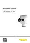
1
EXC-1553PCMCIA MIL-STD-1553 Test and Simulation Card for PCMCIA Compatible Computers User’s Manual 311 Meacham Avenue Elmont NY 11003 e-mail: [email protected] Tel. (516) 327-0000 Fax (516) 327-4645 website: www.mil-1553.com Table of Contents Table of Contents 1 Introduction 1.1 Overview . . . . . . . . . . . . . . . . . . . . . . . . . . . . . . . . . . . . . . . . . . . . . . . . .1-1 1.1.1 EXC-1553PCMCIA Card Features . . . . . . . . . . . . . . . . . . . . . . .1-2 1.2 Installation . . . . . . . . . . . . . . . . . . . . . . . . . . . . . . . . . . . . . . . . . . . . . . . .1-3 1.2.1 Installing the Card . . . . . . . . . . . . . . . . . . . . . . . . . . . . . . . . . . . .1-3 1.2.2 Adding Excalibur Software Tools. . . . . . . . . . . . . . . . . . . . . . . . .1-4 1.3 1553 Bus Connections . . . . . . . . . . . . . . . . . . . . . . . . . . . . . . . . . . . . . .1-5 2 PCMCIA Bus Interface 2.1 Attribute Memory Map . . . . . . . . . . . . . . . . . . . . . . . . . . . . . . . . . . . . . .2-2 2.1.1 Card Information Structure (CIS) . . . . . . . . . . . . . . . . . . . . . . . . .2-2 2.1.2 Function Configuration Registers . . . . . . . . . . . . . . . . . . . . . . . .2-6 2.2 Common Memory Map . . . . . . . . . . . . . . . . . . . . . . . . . . . . . . . . . . . . . .2-7 3 Bus Controller Operation 3.1 Bus Controller Message Processing . . . . . . . . . . . . . . . . . . . . . . . . . .3-2 3.2 Control Registers: BC Mode . . . . . . . . . . . . . . . . . . . . . . . . . . . . . . . . .3-3 3.2.1 Setup Register . . . . . . . . . . . . . . . . . . . . . . . . . . . . . . . . . . . . . . .3-4 3.2.2 Operational Status Register . . . . . . . . . . . . . . . . . . . . . . . . . . . .3-5 3.2.3 Current Command Register. . . . . . . . . . . . . . . . . . . . . . . . . . . . .3-6 3.2.4 Interrupt Mask Register . . . . . . . . . . . . . . . . . . . . . . . . . . . . . . . .3-6 3.2.5 Pending Interrupt Register. . . . . . . . . . . . . . . . . . . . . . . . . . . . . .3-7 3.2.6 Interrupt Log List Pointer Register . . . . . . . . . . . . . . . . . . . . . . . .3-8 3.2.7 BIT Word Register . . . . . . . . . . . . . . . . . . . . . . . . . . . . . . . . . . . .3-8 3.2.8 Minor Frame Time Register . . . . . . . . . . . . . . . . . . . . . . . . . . . . .3-9 3.2.9 Command Block Pointer Register . . . . . . . . . . . . . . . . . . . . . . . .3-9 3.3 Bus Controller Architecture . . . . . . . . . . . . . . . . . . . . . . . . . . . . . . . . .3-10 3.3.1 Control Word . . . . . . . . . . . . . . . . . . . . . . . . . . . . . . . . . . . . . . .3-11 3.3.1.1 3.3.1.2 3.3.2 3.3.3 3.3.4 3.3.5 3.3.6 OPCODE DEFINTION . . . . . . . . . . . . . . . . . . . . . . . . . . . 3-12 BC CONDTION CODES . . . . . . . . . . . . . . . . . . . . . . . . . 3-14 1553 Command Words . . . . . . . . . . . . . . . . . . . . . . . . . . . . . . .3-14 Data Pointer. . . . . . . . . . . . . . . . . . . . . . . . . . . . . . . . . . . . . . . .3-15 1553 Status Words . . . . . . . . . . . . . . . . . . . . . . . . . . . . . . . . . .3-15 Branch Address . . . . . . . . . . . . . . . . . . . . . . . . . . . . . . . . . . . . .3-15 Timer Value . . . . . . . . . . . . . . . . . . . . . . . . . . . . . . . . . . . . . . . .3-15 3.4 Command Block Chaining . . . . . . . . . . . . . . . . . . . . . . . . . . . . . . . . . .3-16 3.5 Memory Architecture . . . . . . . . . . . . . . . . . . . . . . . . . . . . . . . . . . . . . .3-17 3.6 MIL-STD-1553A/B Operation: BC Mode . . . . . . . . . . . . . . . . . . . . . . .3-18 DAS-429PCI/Mx: User’s Manual page i Table of Contents 4 Remote Terminal Operation 4.1 Control Registers . . . . . . . . . . . . . . . . . . . . . . . . . . . . . . . . . . . . . . . . . .4-2 4.1.1 Setup Register . . . . . . . . . . . . . . . . . . . . . . . . . . . . . . . . . . . . . . .4-3 4.1.2 Operational Status Register . . . . . . . . . . . . . . . . . . . . . . . . . . . .4-4 4.1.3 Current Command Block Register . . . . . . . . . . . . . . . . . . . . . . . .4-5 4.1.4 Interrupt Mask Register . . . . . . . . . . . . . . . . . . . . . . . . . . . . . . . .4-5 4.1.5 Pending Interrupt Register. . . . . . . . . . . . . . . . . . . . . . . . . . . . . .4-6 4.1.6 Interrupt Log List Pointer Register . . . . . . . . . . . . . . . . . . . . . . . .4-7 4.1.7 BIT Word Register . . . . . . . . . . . . . . . . . . . . . . . . . . . . . . . . . . . .4-7 4.1.8 Time Tag Register . . . . . . . . . . . . . . . . . . . . . . . . . . . . . . . . . . . .4-8 4.1.9 RT Descriptor Pointer Register . . . . . . . . . . . . . . . . . . . . . . . . . .4-8 4.1.10 1553 Status Word Bits Register . . . . . . . . . . . . . . . . . . . . . . . .4-9 4.1.11 Illegalization Registers. . . . . . . . . . . . . . . . . . . . . . . . . . . . . . .4-10 4.2 Descriptor Block . . . . . . . . . . . . . . . . . . . . . . . . . . . . . . . . . . . . . . . . . .4-12 4.2.1 Receive Control Word . . . . . . . . . . . . . . . . . . . . . . . . . . . . . . . .4-14 4.2.2 Transmit Control Word . . . . . . . . . . . . . . . . . . . . . . . . . . . . . . .4-15 4.2.3 Mode Code Receive Control Word . . . . . . . . . . . . . . . . . . . . . .4-16 4.2.4 Mode Code Transmit Control Word . . . . . . . . . . . . . . . . . . . . . .4-17 4.2.5 Data Pointer A and B (Mode #0) . . . . . . . . . . . . . . . . . . . . . . . .4-18 4.2.6 Ping-pong Handshake . . . . . . . . . . . . . . . . . . . . . . . . . . . . . . . .4-21 4.2.7 Broadcast Data Pointer . . . . . . . . . . . . . . . . . . . . . . . . . . . . . . .4-22 4.3 Data Structures . . . . . . . . . . . . . . . . . . . . . . . . . . . . . . . . . . . . . . . . . . .4-23 4.3.1 Subaddress Receive Data . . . . . . . . . . . . . . . . . . . . . . . . . . . . .4-23 4.3.2 Subaddress Transmit Data . . . . . . . . . . . . . . . . . . . . . . . . . . . .4-24 4.3.3 Mode Code Data . . . . . . . . . . . . . . . . . . . . . . . . . . . . . . . . . . . .4-25 4.4 Mode Code and Subaddress . . . . . . . . . . . . . . . . . . . . . . . . . . . . . . . .4-28 4.5 Encoder and Decoder. . . . . . . . . . . . . . . . . . . . . . . . . . . . . . . . . . . . . .4-30 4.6 RT-to-RT Transfer Compare. . . . . . . . . . . . . . . . . . . . . . . . . . . . . . . . .4-31 4.7 Terminal Address . . . . . . . . . . . . . . . . . . . . . . . . . . . . . . . . . . . . . . . . .4-31 4.8 Reset . . . . . . . . . . . . . . . . . . . . . . . . . . . . . . . . . . . . . . . . . . . . . . . . . . .4-31 4.9 MIL-STD-1553A/B Operation: RT Mode. . . . . . . . . . . . . . . . . . . . . . . .4-32 5 Bus Monitor Operation page ii 5.1 Bus Monitor Message Processing . . . . . . . . . . . . . . . . . . . . . . . . . . . .5-2 5.1.1 Error Condition Message Processing . . . . . . . . . . . . . . . . . . . . .5-2 5.2 Control Registers: BM Mode . . . . . . . . . . . . . . . . . . . . . . . . . . . . . . . . .5-3 5.2.1 Setup Register . . . . . . . . . . . . . . . . . . . . . . . . . . . . . . . . . . . . . . .5-4 5.2.2 Operational Status Register . . . . . . . . . . . . . . . . . . . . . . . . . . . .5-5 5.2.3 Current Command Register. . . . . . . . . . . . . . . . . . . . . . . . . . . . .5-6 5.2.4 Interrupt Mask Register . . . . . . . . . . . . . . . . . . . . . . . . . . . . . . . .5-6 5.2.5 Pending Interrupt Register. . . . . . . . . . . . . . . . . . . . . . . . . . . . . .5-7 5.2.6 Interrupt Log List Pointer Register . . . . . . . . . . . . . . . . . . . . . . . .5-7 5.2.7 BIT Word Register . . . . . . . . . . . . . . . . . . . . . . . . . . . . . . . . . . . .5-8 5.2.8 Time Tag Register . . . . . . . . . . . . . . . . . . . . . . . . . . . . . . . . . . . .5-8 5.2.9 Initial Monitor Block Pointer Register. . . . . . . . . . . . . . . . . . . . . .5-8 5.2.10 Initial Monitor Data Pointer Register . . . . . . . . . . . . . . . . . . . . .5-9 5.2.11 Monitor Block Counter Register. . . . . . . . . . . . . . . . . . . . . . . . .5-9 5.2.12 Monitor Filter Hi Register . . . . . . . . . . . . . . . . . . . . . . . . . . . . . .5-9 5.2.13 Monitor Filter Lo Register . . . . . . . . . . . . . . . . . . . . . . . . . . . .5-10 Excalibur Systems Table of Contents 5.3 Bus Monitor Architecture . . . . . . . . . . . . . . . . . . . . . . . . . . . . . . . . . . .5-11 5.3.1 Message Information Word . . . . . . . . . . . . . . . . . . . . . . . . . . . .5-12 5.3.2 Command Words. . . . . . . . . . . . . . . . . . . . . . . . . . . . . . . . . . . .5-13 5.3.3 Data Pointer. . . . . . . . . . . . . . . . . . . . . . . . . . . . . . . . . . . . . . . .5-13 5.3.4 Status Words . . . . . . . . . . . . . . . . . . . . . . . . . . . . . . . . . . . . . . .5-13 5.3.5 Time Tag . . . . . . . . . . . . . . . . . . . . . . . . . . . . . . . . . . . . . . . . . .5-13 5.3.6 Reserved . . . . . . . . . . . . . . . . . . . . . . . . . . . . . . . . . . . . . . . . . .5-13 5.4 Bus Monitor Block Chaining . . . . . . . . . . . . . . . . . . . . . . . . . . . . . . . .5-14 5.5 Memory Architecture . . . . . . . . . . . . . . . . . . . . . . . . . . . . . . . . . . . . . .5-15 5.6 RT/Concurrent Monitor Operation. . . . . . . . . . . . . . . . . . . . . . . . . . . .5-16 5.7 MIL-STD-1553A/B Operation: BM Mode . . . . . . . . . . . . . . . . . . . . . . .5-17 6 Card Interrupt Architecture 6.1 Overview . . . . . . . . . . . . . . . . . . . . . . . . . . . . . . . . . . . . . . . . . . . . . . . . .6-1 6.1.1 Interrupt Identification Word (IIW) . . . . . . . . . . . . . . . . . . . . . . . .6-2 6.1.2 Interrupt Address Word (IAW) . . . . . . . . . . . . . . . . . . . . . . . . . . .6-2 6.1.3 Interrupt Log List Address . . . . . . . . . . . . . . . . . . . . . . . . . . . . . .6-3 7 Switching Modes of Operation 8 Mechanical And Electrical Specifications 8.1 Mechanical Outline . . . . . . . . . . . . . . . . . . . . . . . . . . . . . . . . . . . . . . . . .8-2 8.2 Connectors . . . . . . . . . . . . . . . . . . . . . . . . . . . . . . . . . . . . . . . . . . . . . . .8-3 8.2.1 25-Pin MIL-STD-1553 I/O Bus Connector Pinout . . . . . . . . . . . .8-3 8.2.2 68-Pin PCMCIA Bus Connector Pinout . . . . . . . . . . . . . . . . . . . .8-4 8.3 Power Requirements . . . . . . . . . . . . . . . . . . . . . . . . . . . . . . . . . . . . . . .8-4 9 Ordering Information DAS-429PCI/Mx: User’s Manual page iii Table of Contents Appendix Appendix A MIL-STD-1553 Word Formats . . . . . . . . . . . . . . . . . . . . . . . . A-1 Appendix B MIL-STD-1553 Message Formats . . . . . . . . . . . . . . . . . . . . . B-1 Figures Figure 1-1 Figure 1-2 Figure 1-3 Figure 1-4 Figure 2-1 Figure 2-2 Figure 3-1 Figure 3-2 Figure 3-3 Figure 3-4 Figure 3-5 Figure 3-6 Figure 3-7 Figure 4-1 Figure 4-2 Figure 4-3 Figure 4-4 Figure 4-5 Figure 4-6 Figure 5-1 Figure 5-2 Figure 5-3 Figure 5-4 Figure 5-5 Figure 8-1 Figure 8-2 Figure 8-3 page iv Inserting the PCMCIA card . . . . . . . . . . . . . . . . . . . . . . . . . 1-3 Direct coupled connection (one bus shown) . . . . . . . . . . . . 1-5 Transformer coupled Connection (one bus shown) . . . . . . . 1-5 MIL-STD-1553 Bus Connection . . . . . . . . . . . . . . . . . . . . . . 1-6 Attribute Memory Map . . . . . . . . . . . . . . . . . . . . . . . . . . . . . 2-2 Common Memory Map . . . . . . . . . . . . . . . . . . . . . . . . . . . . 2-7 Command Block Architecture: BC Mode . . . . . . . . . . . . . . . 3-2 Control Registers Memory Map: BC Mode . . . . . . . . . . . . . 3-3 BC Command Block Architecture . . . . . . . . . . . . . . . . . . . 3-10 Control Word Definition . . . . . . . . . . . . . . . . . . . . . . . . . . . 3-11 Message Control Options . . . . . . . . . . . . . . . . . . . . . . . . . 3-16 Minor Frame Sequencing. . . . . . . . . . . . . . . . . . . . . . . . . . 3-16 Memory Architecture for BC Mode. . . . . . . . . . . . . . . . . . . 3-17 Control Registers Map: RT Mode . . . . . . . . . . . . . . . . . . . . 4-2 Descriptor Table. . . . . . . . . . . . . . . . . . . . . . . . . . . . . . . . . 4-14 RT Non-broadcast Receive Message Indexing . . . . . . . . . 4-20 EXC-1553PCMCIA Descriptor Block – Receive . . . . . . . . 4-21 EXC-1553PCMCIA Descriptor Bock – Transmit . . . . . . . . 4-21 RT Mode #1 Descriptor Block And Circular Buffer. . . . . . . 4-28 Control Registers Map: BM Mode . . . . . . . . . . . . . . . . . . . . 5-3 Bus Monitor Block Diagram . . . . . . . . . . . . . . . . . . . . . . . . 5-11 Message Information Word . . . . . . . . . . . . . . . . . . . . . . . . 5-12 Bus Monitor Block Structuring . . . . . . . . . . . . . . . . . . . . . . 5-14 Memory Architecture for Bus Monitor Mode . . . . . . . . . . . 5-15 Mechanical Outline: EXC-1553PCMCIA Card Layout . . . . . 8-2 EXC-1553PCMCIA-R Card . . . . . . . . . . . . . . . . . . . . . . . . . 8-2 Mechanical Outline: EXC-1553PCMCIA-R . . . . . . . . . . . . . 8-2 Excalibur Systems Chapter 1 1 Introduction Introduction Chapter 1 provides an overview of the EXC-1553PCMCIA avionics communication card. 1.1 Overview . . . . . . . . . . . . . . . . . . . . . . . . . . . . . . . . . . . . . . . . . . .1-1 1.1.1 1.2 Installation . . . . . . . . . . . . . . . . . . . . . . . . . . . . . . . . . . . . . . . . . .1-3 1.2.1 1.2.2 1.3 1.1 EXC-1553PCMCIA Card Features . . . . . . . . . . . . . . . . . . .1-2 Installing the Card . . . . . . . . . . . . . . . . . . . . . . . . . . . . . . . .1-3 Adding Excalibur Software Tools . . . . . . . . . . . . . . . . . . . .1-4 1553 Bus Connections . . . . . . . . . . . . . . . . . . . . . . . . . . . . . . . .1-5 Overview The EXC-1553PCMCIA is an intelligent, memory-mapped MIL-STD-1553 interface card which complies with the Personal Computer Memory Card International Association (PCMCIA Release 2.1) standard, including Plug and Play. The card’s small size and suitability for PCMCIA compatible notebook computers with Type II slots make it a complete solution for developing and testing 1553 interfaces and for performing system simulation of the MIL-STD-1553 bus, both in the lab and in the field. The EXC-1553PCMCIA is designed around the UT69151 DX (UTMC’s SUMMIT™ LX/DX 1553 Controller. The EXC-1553PCMCIA contains 64K words of dual-port RAM and an additional 32 words of Control registers, all mapped within the Common memory space. The unit also contains an EEPROM-based Card Information Structure (CIS) within the Attribute Memory space. The card gives the user direct access to the memory-mapped control registers in the SUMMIT™ chip and the Control registers in the dual-port RAM. Operation of the card is controlled by accessing the Control registers, which can be modified, along with the data, in real-time. The EXC-1553PCMCIA comes complete with GUI software, a C-driver software library including the source code and an adapter cable assembly. The EXC-1553PCMCIA-R is the same as the EXC-1553PCMCIA with a ruggedized, hard-wired cable connection. For a diagram of the hard-wired connection see Figure 8-2 EXC-1553PCMCIA-R Card on page 8-2. For ordering information see Chapter 9: Ordering Information. EXC-1553PCMCIA: User’s Manual page 1 - 1 Chapter 1 1.1.1 Introduction EXC-1553PCMCIA Card Features Operates as BC, RT, Bus Monitor and RT/ Concurrent Monitor Complies with PCMCIA standard release 2.1 Multiple protocol capability: PCMCIA Type I PC card MIL-STD-1553A MIL-STD-1553B Plug and Play compatible 64K Words memory-mapped, dual-port RAM 5 Volt supply only Message illegalization Power down mode for low power consumption Real-time operation All logic self-contained; no external module required Polling or Interrupt driven EEPROM based Card Information Structure Programmable Broadcast mode 16-bit Time Tag Major and Minor frames GUI software Programmable Intermessage Gap C software library included For exact part numbers see Chapter 9: Ordering Information. page 1 - 2 Excalibur Systems Chapter 1 1.2 Introduction Installation To operate the EXC-1553PCMCIA card 1. 2. Install the card in the computer Add MCH Software Tools to your system. Installation of the EXC-1553PCMCIA card is similar to that of all PCMCIA slot. The EXC-1553PCMCIA complies with the “Plug and Play” specification of the PCI standard. As such, its absolute address is determined by the BIOS at start-up. Warning Wear an suitably grounded electrostatic discharge wrist strap whenever handling an Excalibur card and use all necessary antistatic precautionary measures. 1.2.1 Installing the Card Note: The adapter cable assembly may be connected to the card either before or after the card is inserted into the PCMCIA slot on the computer. In addition, the cable assembly may be connected to and disconnected from the card while power to the computer is turned on, but not while the card is transmitting over the bus. 1. 2. Open the expansion slot cover. Insert the EXC-1553PCMCIA card with the label facing up. (See Figure 1-1) When the card is almost all the way in the slot, push firmly but gently to ensure a firm connection with the computer. Do not force the card into position. EXC-1553PCMCIA Card Figure 1-1 Inserting the PCMCIA card EXC-1553PCMCIA: User’s Manual page 1 - 3 Chapter 1 Introduction 3. 4. 1.2.2 Connect the adapter cable assembly to the EXC-1553PCMCIA card. Push the latch button on the top of the cable connector to secure it. Verify that the connector is in place. Adding Excalibur Software Tools The software and documentation on the Excalibur Installation CD you received with your package, is the most recent release as of the date of shipping. Further up-dates and new releases can be found and downloaded from our website: www-1553.com. The standard software provided with Excalibur boards and modules is for Windows operating systems. Other operating systems are available. Check on our website or write to [email protected]. For information about adding the accompanying software drivers, see the readme.pdf file on the Excalibur Installation CD that came with the EXC-1553PCMCIA card. page 1 - 4 Excalibur Systems Chapter 1 1.3 Introduction 1553 Bus Connections The EXC-1553PCMCIA contains a 25-pin MIL-STD-1553 I/O bus connector. Each board is shipped with an adapter cable that converts the rear connector to a standard 1553 [miniature] female twinax type. The adapter cable comes wired and ready to connect to the 1553 card (buses A and B0. the 1553 connectors will mate, for example, with the Trompeter PL75 male twinax connector which is not supplied but can be ordered from Excalibur Systems. For short distances, direct coupling may be used to connect the EXC-1553PCMCIA directly to another 1553 device. To ensure data integrity, you must make certain that the cable connecting the two devices is properly terminated with 78-Ohm resistors (see Figure 1-2). High 78 Ohm Terminating Resistors Low EXC-1553PCMCIA Direct Coupled Figure 1-2 1553 Device Transformer Coupled Direct coupled connection (one bus shown) If operating in the more standard Transformer coupling mode, use stub coupler devices, which are available from Excalibur Systems. Two terminators are required for each coupler, which services a single bus, i.e. BUS A (see Figure 1-3). For more information see our website: www.mil-1553.com. To other 1553 device Hi EXC-1553PCMCIA Transformer Coupled Lo s-A Terminator 78 Ohm Figure 1-3 s-B 1553 Device Transformer Coupled s-C Three Stub Coupler Terminator 78 Ohm Transformer coupled Connection (one bus shown) EXC-1553PCMCIA: User’s Manual page 1 - 5 Chapter 1 Introduction Example of MIL-STD-1553 Bus Connection 78 BUS B Terminator 78 Terminator BUS A Stub Coupler Bus BUS A Bus 1553 DEVICE #n BUS B Stub Coupler Bus Stub Bus Stub Coupler Bus BUS A Bus 1553 DEVICE #2 Stub Stub TEST COMPUTER 78 Stub Coupler MIL-STD-1553 TEST CARD Stub BUS B Bus Terminator 78 1553 DEVICE #1 BUS B BUS A Bus Terminator Stub Stub Coupler Stub Coupler Bus BUS A Stub Bus Bus Stub BUS B Bus Rev A Oct. 24, 2000 Figure 1-4 page 1 - 6 MIL-STD-1553 Bus Connection Excalibur Systems Chapter 2 2 PCMCIA Bus Interface PCMCIA Bus Interface Chapter 2 describes the PCMCIA bus interface. The following topics are covered: 2.1 Attribute Memory Map. . . . . . . . . . . . . . . . . . . . . . . . . . . . . . . . .2-2 2.1.1 2.1.2 2.2 Card Information Structure (CIS) . . . . . . . . . . . . . . . . . . . . . . . .2-2 Function Configuration Registers . . . . . . . . . . . . . . . . . . . . . . . .2-6 Common Memory Map . . . . . . . . . . . . . . . . . . . . . . . . . . . . . . . .2-7 The PCMCIA standard defines the electrical and physical interface between the PC Card and the host computer, including the 68-pin connector. Detailed specifications can be found in the PCMCIA PC Card Standard. The EXC-1553PCMCIA supports two types of address spaces: • Attribute Memory Map space, for the Card Information Structure (CIS) and the Function Configuration Registers. • Common Memory Map space, for regular memory accesses. The dual-port RAM and the Time Tag counter are located in Common Memory. The Attribute Memory space is selected by driving the signal REG# low, and the Common Memory space is selected by driving the signal REG# high (see Tables 2-1 and 2-2 for details regarding memory access). FUNCTION REG# CE2# CE1# A0# OE# WE# D15-D8 D7-D0 Standby X H H X X X Hi-Z Hi-Z Lo Byte Read H H L L L H Hi-Z Even-Byte Lo Byte Write H H L L H L Hi-Z Even-Byte Hi Byte Read H L H X L H Odd-Byte Hi-Z Hi Byte Write H L H X H L Odd-Byte Hi-Z Word Read H L L X L H Odd-Byte Even-Byte Word Write H L L X H L Odd-Byte Even-Byte Table 2-1 Common Memory Access for EXC-1553PCMCIA FUNCTION REG# CE2# CE1# A0# OE# WE# D15-D8 D7-D0 Standby X H H X X X Hi-Z Hi-Z Lo Byte Read L H L L L H Hi-Z Even-Byte Lo Byte Write L H L L H L Hi-Z Even-Byte Hi Byte Read L L H X L H Invalid Hi-Z Hi Byte Write L L H X H L Invalid Hi-Z Word Read L L L X L H Invalid Even-Byte Word Write L L L X H L Invalid Even-Byte Table 2-2 Note: Attribute Memory Access for EXC-1553PCMCIA The EXC-1553PCMCIA does not support odd-byte access to data lines D7–D0. EXC1553PCMCIA: User’s Manual page 2 - 1 Chapter 2 PCMCIA Bus Interface Information concerning the format of the card is stored in the Card Information Structure (CIS). The CIS is a variable-length, linked-list of data blocks, called tuples. The CIS resides in even bytes of the Attribute Memory, beginning at address 0. Two function configuration registers are located in the Attribute Memory. The configuration registers are also in the Common Memory. These allow the user to reset the EXC-1553PCMCIA card, service interrupts, etc. 2.1 Attribute Memory Map The Attribute Memory is selected during an even-byte or word access when the host drives the signal REG# low. The Attribute Memory contains the CIS and two Function Configuration Registers. The CIS is read-only. The CIS resides in the even-bytes starting at address 0 and ending when the End of List tuple is encountered. The two Function Configuration Registers are located at addresses 40000 (H) and 40002 (H). The region above the CIS and the Function Configuration Registers is reserved and should not be accessed. FUNCTION CONFIGURATION REGISTERS [Configuration Status Register Configuration Option Register] [40002 H 40000 H] CARD INFORMATION STRUCTURE (CIS) 00000–3FFFF H Figure 2-1 2.1.1 Attribute Memory Map Card Information Structure (CIS) The Card Information Structure (CIS) contains information about the type of PC card (memory or I/O), the types and sizes of memory, and the interface to the host. Information is stored in a variable-length linked-list of data blocks, called tuples. The first byte of each tuple contains the tuple code, which defines what type of information the tuple provides. The next byte is the link byte, which indicates how many bytes remain in the current tuple. 2.1.1.1 Device Tuple for Common Memory The first tuple identifies the card as a 5V PCMCIA card. 2.1.1.2 Level 1 Version/Product Information Tuple This tuple contains Level-1-version compliance information as defined in PCMCIA Release 2.0, and information about the card manufacturer. Included are the major version number and the minor version number, [04 (H) and 01 (H) respectively, according to PCMCIA Release 2.0]. Also included are the manufacturer name and the product name. 2.1.1.3 Manufacture Identification Tuple This tuple contains Excalibur System’s Manufacturer Code, which is 0145 (H). Also included is the current revision of the CIS table. The revision of the CIS is read as hex numbers. For example, revision 1.0 would be read as 10 (H). page 2 - 2 Excalibur Systems Chapter 2 PCMCIA Bus Interface 2.1.1.4 Configuration Tuple This tuple establishes the number and address of the Function Configuration Registers, and indicates the index of the last Configuration Entry Tuple. The EXC1553PCMCIA has two Configuration Registers at base address 40000 (H). The index of the last Configuration Entry Tuple is 2. 2.1.1.5 Configuration Entry Tuple This tuple describes the type of interface utilized by the EXC-1553PCMCIA. • Under Windows 9x/ME/2000/XP: from the inf file on the Excalibur Installation CD. • Windows NT4: from a registry entry written by the Excalibur Configuration Utility (ExcConfig.exe) For more information about the accompanying drivers, see MCH Family Software Tools - Programmers Reference. 2.1.1.6 No Link Tuple This tuple indicates that the CIS doesn’t continue in another linked list after the End of List tuple. 2.1.1.7 End of List Tuple This tuple indicates the end of the linked list. EXC1553PCMCIA: User’s Manual page 2 - 3 Chapter 2 PCMCIA Bus Interface 2.1.1.8 CIS Table Tuple Address Tuple Value Tuple Field Name General Description 00 H 01 H TPL_CODE CISTPL_DEVICE 02 H 01 H TPL_LNK 04 H FF H End of Tuple 06 H 15 H TPL_CODE CISTPL_VERS_1 08 H 2C H TPL_LNK 0A H 04 H TPLLV1_MAJOR Major version number (04 H) 0C H 01 H TPLLV1_MINOR Minor version number (01 H) 0E H 45 H ”E” Name Of Manufacturer 10 H 78 H ”x” 12 H 63 H ”c” 14 H 61 H “a” 16 H 6C H “l” 18 H 69 H “i” 1A H 62 H “b” 1C H 75 H “u” 1E H 72 H “r” 20 H 20 H “space” 22 H 53 H “S” 24 H 79 H “Y” 26 H 73 H “s” 28 H 74 H “t” 2A H 65 H “e” 2C H 6D H “m” 2E H 73 H “s” 30 H 20 H “space” 32 H 49 H “I” 34 H 6E H “n” 36 H 63 H “c” 48 H 2E H “.” 3A H 00 H “terminator” 3C H 44 H “E” 3E H 41 H “X” 40 H 53 H “C” 42 H 2D H “-” 44 H 34 H “1” 46 H 32 H “5” 48 H 39 H “5” 4A H 50 H “3” 4C H 43 H “P” 4E H 40 H “C” 50 H 43 H “M” Name of Product CIS Table page 2 - 4 Excalibur Systems Chapter 2 PCMCIA Bus Interface Tuple Address Tuple Value 52 H 49 H Tuple Field Name General Description “C” 54 H 41 H “I” 56 H 2F H “A” 58 H 52 H “/” 5A H 54 H “B” 5C H 78 H “terminator” 5E H 00 H End of Tuple 60 H 20 H TPL_CODE 62 H 04 H TPL_LNK CISTPL_MANFID 64 H 45 H TPLMID_MANF Manufacturer code for Excalibur Systems Lo 66 H 01 H TPLMID_MANF Manufacturer code for Excalibur Systems Hi 68 H 00 H 6A H *** 6C H 6E H Reserved CIS Revision *** Revision of CIS (Rev. 1.0 is read as 10 H) 1A H TPL_CODE CISTPL_CONFIG 06 H TPL_CODE 70 H 02 H TPCC_SZ 3 address bytes for Configuration Registers 72 H 02 H TPCC_LAST Index number of last entry is 2 74 H 00 H TPCC_RADR Configuration Registers Base Address Lo 76 H 00 H TPCC_RADR Configuration Registers Base Address Mid 78 H 04 H TPCC_RADR Configuration Registers Base Address Hi 7A H 03 H TPCC_RMSK First two Configuration Registers CISTPL_CFTABLE_ENTRY 7C H 1B H TPL_CODE 7E H 0E H TPL_LNK 80 H C2 H TPCE_INDX Interface follows, Set Default, Index is 2 82 H 80 H TPCE_IF WAIT, No Rdy/Bsy, WP, BVD, Memory Type Interface 84 H 62 H TPCE_FS Memory description follows, no IRQ, VCC and VPP power description 86 H 01 H TPCE_PD VCC nominal voltage 88 H 55 H TPCE_PD VCC: 5V 8A H 01 H TPCE_PD VPP nominal voltage 8C H 0E H TPCE_PD VPP: 12V 8E H 49 H TPCE_MS 2 bytes address size, 1 byte length, 2 window description 90 H 80 H TPCE_MS Window 1 length size = 32K 92 H 00 H TPCE_MS WIndows 1 address = 000000 H 94 H 00 H TPCE_MS 96 H 01 H TPCE_MS Windows 2 length size 1/4K 98 H 00 H TPCE_MS Windows 2 address = 040000 H 9A H 04 H TPCE_MS 9C H 14 H TPL_CODE 9E H 00 H TPL_LINK A0 H FF H TPL_CODE CISTPL_NO_LINK CISTPL_END CIS Table (cont.) EXC1553PCMCIA: User’s Manual page 2 - 5 Chapter 2 2.1.2 PCMCIA Bus Interface Function Configuration Registers The two function configuration registers, located in the Attribute Memory, allow the user to reset the EXC-1553PCMCIA card or to service interrupts. 2.1.2.1 Configuration Option Register Address: 40000 (H) Read/Write Bit Bit Name Description 07 Software Reset 1 = Resets the EXC-1553PCMCIA. This bit remains high, and the card remains in reset mode, until a 0 is written to this bit. The default value of the reset bit is 0. 06 Reserved Set to 1 on read – Ignore on write. 02-05 Reserved Set to 0 on write – Ignore on read 01 RT Lock 1 = Locks the card into RT mode 0 = Select a mode via the software – Ignore on read 00 Reserved Set to 0 on write – Ignore on read. Configuration Option Register 2.1.2.2 Configuration & Status Register Address: 40002 (H) Read/Write Bit Bit Name Description 02-07 Reserved Set to 0 on write. Ignore on read. 01 Interrupt Pending 1 = The EXC-1553PCMCIA has an interrupt waiting to be serviced. This bit remains high, and the card remains in interrupt pending mode, until a 0 is written to this bit. Writing a 1 to this bit has no effect on the value of the bit. The default value of the interrupt pending bit is 0. 00 Reserved Set to 0 on write. Ignore on read. Configuration & Status Register page 2 - 6 Excalibur Systems Chapter 2 2.2 PCMCIA Bus Interface Common Memory Map The Common Memory contains 128KB of dual-port RAM and 32 Words of Control registers. The RAM may be accessed in either Byte or Word mode, while the Control registers must be accessed in Word mode. The region between the RAM and the Control Registers is reserved. FUNCTION CONFIGURATION REGISTERS [Configuration Status Register Configuration Option Register] [40042 H 40040 H] CONTROL REGISTERS 40000 - 4003F H RESERVED 20000 - 3FFFF H DUAL-PORT RAM 00000–1FFFF H Figure 2-2 Common Memory Map Chapters 3, 4, and 5 of the User’s Manual explain EXC-1553PCMCIA operation in Bus Controller mode, Remote Terminal mode and Bus Monitor mode. In each chapter the mode specific Control Registers and Memory Block are described. EXC1553PCMCIA: User’s Manual page 2 - 7 Chapter 2 PCMCIA Bus Interface page 2 - 8 Excalibur Systems Chapter 3 3 Bus Controller Operation Bus Controller Operation Chapter 3 describes EXC-1553PCMCIA operation in Bus Controller (BC) mode. 3.1 Bus Controller Message Processing . . . . . . . . . . . . . . . . . . . . 3-2 3.2 Control Registers: BC Mode . . . . . . . . . . . . . . . . . . . . . . . . . . . 3-3 3.3 Bus Controller Architecture. . . . . . . . . . . . . . . . . . . . . . . . . . . 3-10 3.3.1 3.3.2 3.3.3 3.3.4 3.3.5 3.3.6 Control Word . . . . . . . . . . . . . . . . . . . . . . . . . . . . . . . . . . . . . . 3-11 1553 Command Words . . . . . . . . . . . . . . . . . . . . . . . . . . . . . . 3-14 Data Pointer . . . . . . . . . . . . . . . . . . . . . . . . . . . . . . . . . . . . . . . 3-15 1553 Status Words. . . . . . . . . . . . . . . . . . . . . . . . . . . . . . . . . . 3-15 Branch Address . . . . . . . . . . . . . . . . . . . . . . . . . . . . . . . . . . . . 3-15 Timer Value . . . . . . . . . . . . . . . . . . . . . . . . . . . . . . . . . . . . . . . 3-15 3.4 Command Block Chaining . . . . . . . . . . . . . . . . . . . . . . . . . . . . 3-16 3.5 Memory Architecture . . . . . . . . . . . . . . . . . . . . . . . . . . . . . . . . 3-17 3.6 MIL-STD-1553A/B Operation: BC Mode . . . . . . . . . . . . . . . . . 3-18 EXC-1553PCMCIA: User’s Manual page 3 - 1 Chapter 3 3.1 Bus Controller Operation Bus Controller Message Processing To process messages, the EXC-1553PCMCIA uses data supplied in the control registers along with data stored in memory. The EXC-1553PCMCIA accesses eight 16-bit words stored in memory called a Command Block. The Command Block is accessed at the beginning and end of a command processing. Note In BC mode, EXC-1553PCMCIA does not need to re-read the Command Block on a retry situation. The user allocates memory spaces for the minor frame. The top of the Command Blocks can reside at any address location. Defined and entered into memory by the user, the Control registers are linked to the Command Block via the Command Block Pointer Register contents. Each command block contains a: Control Word Command Word1 Command Word2 Data Pointer Status Word 1 Status Word 2 Branch Address Timer Value Figure 3-1 Command Block Architecture: BC Mode See section See Bus Controller Architecture, page 3-10, for a description of each location. Control Word information allows the EXC-1553PCMCIA to control the commands transmitted over the 1553 bus. The Control word allows the EXC-1553PCMCIA to transmit commands on a specific bus, perform retries, initiate RT-to-RT transfers, and interrupt on certain conditions. The host defines each Command Word associated with each command block. For normal 1553 commands, only the first Command Word location will contain valid data. For RT-to-RT commands, as specified in the Control Word, the host must define the first Command Word as a receive and the second Command Word as a transmit. For a receive command, the Data Pointer is read to determine where Data Words are retrieved. The EXC-1553PCMCIA retrieves Data Words sequentially from the address specified by the Data Pointer. For a transmit command, the Data Pointer is read to determine the top memory location. The card stores Data Words sequentially from this top memory location. The EXC-1553PCMCIA reads the command block during minor frame processing. The card then begins the acquisition of Data Words for either transmission or storage. After transmission or reception, the EXC-1553PCMCIA begins post-processing. The Command Block is updated. The card modifies the Control Word as required. An optional interrupt log entry is performed after the Command Block update. page 3 - 2 Excalibur Systems Chapter 3 3.2 Bus Controller Operation Control Registers: BC Mode The control registers are read/write unless otherwise stated. All control registers must be accessed in Word mode. All Control register bits are active high and are reset to 0 unless otherwise stated. Figure 3-2 below illustrates the control registers for Bus Controller mode. Reserved 40012 - 4003F H Command Block Pointer Register 40010 H Minor Frame Timer 4000E H BIT Word Register 4000C H Interrupt Log List Pointer Register 4000A H Pending Interrupt Register 40008 H Interrupt Mask Register 40006 H Current Command Block Register 40004 H Operational Status Register 40002 H Control Register 40000 H Figure 3-2 Control Registers Memory Map: BC Mode EXC-1553PCMCIA: User’s Manual page 3 - 3 Chapter 3 3.2.1 Bus Controller Operation Setup Register Address: 40000 (H) Read/Write The Setup Register configures the EXC-1553PCMCIA for operation. To make changes to the BC and this register, the STEX bit (bit 15) must be logic 0. Bit Bit Name Description 15 STEX Start Execution 1 = Initiates EXC-1553PCMCIA operation 0 = Inhibits EXC-1553PCMCIA operation After execution begins, writing a logic 0 will halt the card after completing the current 1553 message. 14 SBIT Start BIT 1 = Places the card into the Built-In Test routine. The BIT test takes 1 msec. to execute and has a fault coverage of 93.4%. Once the card has been started, the host must halt the card in order to place it into the Built-In Test mode (STEX = 0). Note If Start BIT (SBIT) and Start Execution (STEX) are both set on one register write, BIT has priority. 13 SRST Software Reset 1 = Performs a software reset. the Configuration registers are not affected when this bit is asserted. The software reset takes 6 µsec. to execute. 05-12 Reserved Set to 0 04 BCEN Broadcast Enable 1 = Enables the broadcast option for BC Mode. 0 = Enables Remote Terminal #31 as a unique remote terminal address. When enabled, the card does not expect a Status Word response from the Remote Terminal. 03 Reserved Set to 0 02 PPEN Ping-Pong Enable. This bit controls the method by which the card will retry messages. 1 = Allows the card to ping-pong between buses during retries. 0 = All retries will be performed on the programmed bus as defined in the Retry Number field of the Command Block control word. 01 INTEN Interrupt Log List Enable. 1 = Enables the interrupt log list. 0 = Prevents the logging of interrupts as they occur. 00 Reserved Set to 0 Setup Register page 3 - 4 Excalibur Systems Chapter 3 3.2.2 Bus Controller Operation Operational Status Register Address: 40002 (H) Read/Write The Operational Status Register provides pertinent status information for BC Mode and is reset to ED82 H. Note To make changes to the BC and this register, the STEX bit (Bit 15 in the Setup Register) must be logic 0. Bit Bit Name Description 10-15 Reserved Set to 0 09 MSEL1 Mode Select 1. In conjunction with Mode Select 0, this bit determines the card’s mode of operation. 08 MSEL0 Mode Select 0. In conjunction with Mode Select 1, this bit determines the card's mode of operation. MSEL1 MSEL0 Mode of Operation 0 0 BC 0 1 RT 1 0 BM 1 1 RT/ Concurrent BM 07 A/B_STD Military Standard 1553A or 1553B. This bit determines if the card will operate under MIL-STD-1553A or 1553B protocol. 1 = Forces the card to look for all responses in 9 µsec. or generate time-out errors. 0 = Automatically allows the card to operate under the MIL-STD-1553B protocol (see section 3.6 MIL-STD-1553A/B Operation: BC Mode, on page 3-18, 04-06 Reserved These read-only bits are not applicable. 03 EX Card Executing – read only 1 = The card is executing. 0 = The card is idle. 02 Reserved This read-only bit is not applicable. 01 Ready Card-Ready. This read-only bit is cleared on reset. 1 = The card has completed initialization or BIT, and regular operation may begin. 00 TERACT Card Terminal Active. This read-only bit is cleared on reset. 1 = The card is presently processing a 1553 message. Note When STEX transitions from 1 to 0, EX and TERACT stay active until command processing is complete. Operational Status Register EXC-1553PCMCIA: User’s Manual page 3 - 5 Chapter 3 3.2.3 Bus Controller Operation Current Command Register Address: 40004 (H Read only The Current Command register contains the last 1553 command that was transmitted by the card. Upon the execution of each Command Block, this register will automatically be updated. This register is updated when transmission of the Command Word begins. In an RT-to-RT transfer, the register will reflect the latest Command Word as it is transmitted. Bit Bit Name Description 00-15 CC[15-0] Current Command. These bits contain the latest 1553 command that was transmitted by the Bus Controller. Current Command Register 3.2.4 Interrupt Mask Register Address: 40006 (H) Read/Write The BC Mode interrupt architecture allows the host to mask or temporarily disable the service of interrupts. While masked, interrupt activity does not occur. The unmasking of an interrupt after the event occurs does not generate an interrupt for that event. An interrupt is masked only if the corresponding bit of this register is set to a logic 0. Bit Bit Name Description 15 DMAF DMA Fail Interrupt 14 WRAPF Wrap Fail Interrupt 13 Reserved Set to 0 12 BITF BIT Fail Interrupt 11 MERR Message Error Interrupt 06-10 Reserved Set to 0 05 EOL End Of List Interrupt 04 ILLCMD Illegal Command Interrupt 03 ILLOP Illogical Opcode Interrupt 02 RTF Retry Fail Interrupt 01 CBA Command Block Accessed Interrupt 00 Reserved Set to 0 Interrupt Mask Register page 3 - 6 Excalibur Systems Chapter 3 3.2.5 Bus Controller Operation Pending Interrupt Register Address: 40008 (H) Read only The Pending Interrupt register is used to identify which of the interrupts occurred during operation. A 125 nsec. interrupt is generated when any bit in this register is set by the card. Note All register bits are cleared on a host read. Bit Bit Name Description 15 DMAF DMA Fail Interrupt – Indicates that a memory access failed. 14 WRAPF Wrap Fail Interrupt 1 = The card automatically compares the transmitted word (encoder word) to the reflected decoder word by way of the continuous loopback feature. If the encoder word and reflected word do not match, the WRAPF bit is set and an interrupt is generated. The loopback path is via the MIL-STD-1553 bus transceiver. 13 Reserved Ignore on read 12 BITF BIT Fail Interrupt 1 = A BIT failure. Interrogate Bit Word register bits 11 and 10 to determine the specific channel that failed. In BC mode an interrupt is generated and command processing stops if initiated by opcode. 11 MERR Message Error Interrupt 1 = A message error occurred. The card can detect Manchester, sync-field, word count, 1553 word parity, bit count, and protocol errors. This bit will be set and an interrupt generated (if not masked) after message processing is complete. 06-10 Reserved Ignore on read. 05 EOL End Of List Interrupt. 1 = The card is at the end of the command block. 04 ILLCMD Illogical Command Interrupt The card checks for RT-to-RT Terminal address field match, RT-to-RT transmit/receive bit mismatch and correct order, and broadcast transmit commands. If illogical commands occur, the card will halt execution. An interrupt is generated 1 = An illogical command (i.e., Transmit Broadcast or improperly formatted RT-to-RT message) has been written into the Command Block. 03 ILLOP Illogical Opcode Interrupt. 1 = An illogical opcode (i.e., any reserved opcode) was used in the Command Block. The card halts operation if this condition occurs. 02 RTF Retry Fail Interrupt. 1 = All programmed retries failed. 01 CBA Command Block Accessed Interrupt. 1 = A Command Block was accessed (Opcode 1010), if enabled. 00 Reserved Ignore on read. Pending Interrupt Register EXC-1553PCMCIA: User’s Manual page 3 - 7 Chapter 3 3.2.6 Bus Controller Operation Interrupt Log List Pointer Register Address: 4000A (H) Read/Write The Interrupt Log List Pointer indicates the starting address of the Interrupt Log List. The Interrupt Log List is a 32-word ring-buffer that contains information pertinent to the service of interrupts. The EXC-1553PCMCIA architecture requires the location of the Interrupt Log List on a 32-word boundary. The most significant 11 bits of this register designate the location of the Interrupt Log List within a 64K-word memory space. Initialize the lower 5 bits of this register to a logic 0 by the host. The card controls the lower 5 bits to implement the ring-buffer architecture. Read this register to determine the location and number of interrupts within the Interrupt Log List (least significant 5 bits). Bit Bit Name Description 00-15 ILLP[15-0] Interrupt Log List Pointer Bits. Note Bits 05-15 indicate the starting Base address while bits 00-04 indicate the ring location of the Interrupt Log List. Interrupt Log List Pointer Register 3.2.7 BIT Word Register Address: 4000C (H) Read/Write The BIT Word register contains information on the current status of the EXC-1553PCMCIA. The user defines the lower 8 bits of this register. Bit Bit Name Description 15 DMAF DMA Fail. 1 = All the card's internal DMA activity was not completed within 16 µsec. 14 WRAPF Wrap Fail. The card automatically compares the transmitted word (encoder word) to the reflected decoder word by way of the continuous loop-back feature. If the encoder word and reflected word do not match, the WRAPF bit is set. The loopback path is via the MIL-STD-1553 bus transceiver. 13 Reserved Ignore on read 12 BITF BIT Fail. 1 = A BIT failure. Interrogate bits 11 and 10 to determine the specific channel that failure. 11 CHAF Channel A Fail. 1 = A BIT test failure in Channel A. 10 CHBF Channel B Fail. 1 = A BIT test failure in Channel B. 00-09 Reserved Ignore on Read BIT Word Register page 3 - 8 Excalibur Systems Chapter 3 3.2.8 Bus Controller Operation Minor Frame Time Register Address: 4000E (H) Read only The Minor Frame Timer register (MFT) reflects the state of the 16-bit MFT counter. This counter is loaded via the Load Minor Frame Timer opcode (Opcode 1110). Bit Bit Name Description 00-15 MFT[15-0] Minor Frame Timer. These bits indicate the value of the timer. Minor Frame Time Register 3.2.9 Command Block Pointer Register Address: 40010 (H) Read/Write The Command Block Pointer register contains the location to start the Command Blocks. After execution begins, this register is automatically updated with the address of the next block. Bit Bit Name Description 00-15 CBA[15-0] Command Block Address. These bits indicate the starting location of the Command Block. Command Block Pointer Register EXC-1553PCMCIA: User’s Manual page 3 - 9 Chapter 3 3.3 Bus Controller Operation Bus Controller Architecture As defined in MIL-STD-1553, the Bus Controller initiates all communications on the bus. To comply with MIL-STD-1553 bus controller requirements, the EXC-1553PCMCIA uses a Command Block architecture that takes advantage of both control registers and RAM. Each Command Word transmitted over the bus must be associated with a Command Block. The Command Block requires eight contiguous 16-bit memory locations for each message. These eight locations include a: Control Word 1st location Command Word1 2nd location Command Word2 Data Pointer Status Word 1 Status Word 2 Branch Address Timer Value Figure 3-3 8th location BC Command Block Architecture The host must initialize each of the locations associated with each Command Block. The exception is for the two status locations that will be updated as Command Words are transmitted and corresponding Status Words are received. Command Blocks may be linked together in such a manner as to allow the generation of Major and Minor message frames. In addition, the BC can detect the assertion of Status Word bits and generate interrupts or branch to a new message frame, depending of course, on the specific conditions that arise. page 3 - 10 Excalibur Systems Chapter 3 3.3.1 Bus Controller Operation Control Word The first memory location of each BC Mode Command Block contains the Control word. Each control word contains the opcode, retry number, bus definition, RT-to-RT instruction, condition codes, and the block access message error. The control word is defined below: 15 12 Opcode Figure 3-4 11 10 Retry # 09 08 BUSA/B RT-RT 07 01 00 Conditions Codes Block Access ME Control Word Definition Bit Bit Name Description 12-15 Opcode These bits define the opcode to be used by the card for that particular Command Block. If the opcode does not perform any 1553 function, all other bits are ignored. Each of the available opcodes is defined in section 3.3.1.1 OPCODE DEFINTION, on page 3-12, 10-11 Retry Number These bits define the number of retries for each individual Command Block and if retry opcode is used. If the Ping-Pong Enable Bit (bit 02 of the Control Register) is not enabled, all retries will occur on the programmed bus. However, if bit 02 is enabled, the first retry will always occur on the alternate bus, the second retry will occur on the primary bus, the third retry will occur on the alternate bus, and the fourth retry will occur on the primary bus. Bit 11 Bit 10 No. of Retries 0 1 1 0 1 0 1 0 1 2 3 4 09 Bus A/B This bit defines on which of the two buses the command will be transmitted (i.e., primary bus). (Logic 1 = Bus A, Logic 0 = Bus B). 08 RT-RT Transfer This bit defines whether or not the present Command Block is an RT-toRT transfer and if the card should transmit the second Command word. Data associated with an RT-to-RT is always stored by the card. 01-07 Condition Codes These bits define the condition code the EXC-1553PCMCIA uses for that particular Command Block. Each of the available condition codes is defined in section 3.3.1.2 BC CONDTION CODES, on page 3-14, 00 Block Access Message Error The card sets this bit to 1, indicating a protocol message error occurred in the RT’s response. For this occurrence, the card will overwrite this bit prior to storing the Control Word into memory. An example of this type of error would be noise on the 1553 bus. Control Word Description EXC-1553PCMCIA: User’s Manual page 3 - 11 Chapter 3 3.3.1.1 Bus Controller Operation OPCODE DEFINTION Opcode Field Name Definition 0000 End Of List This opcode instructs the card that the end of the command block has been encountered. Command processing stops and the interrupt is generated if the interrupt is enabled. No command processing takes place (i.e., no 1553). 0001 Skip This opcode instructs the card to load the message-to-message timer with the value stored in timer value location. The card will then wait the specific time before proceeding to the next command block. This opcode allows for scheduling a specific time between message execution. No command processing takes place (i.e., no 1553). 0010 Go To This opcode instructs the card to “go to” the command block as specified in the branch address location. No command process takes place (i.e., no 1553). 0011 Built-in Test This opcode instructs the SUMMIT chip to perform an internal built-in test. If the card passes the built-in test, then processing of the next command block will continue. However, if the card fails the built-in test, then processing stops. No command processing takes place (i.e., no 1553). 0100 Execute Block; Continue This opcode instructs the card to execute the current command block and proceed to the next command block. This opcode allows for continuous operations. 0101 Execute Block; Branch This opcode instructs the card to execute the current command block and unconditionally branch to the location as specified in the branch address location. 0110 Execute Block; Branch on Condition This opcode instructs the card to execute the current command block and branch only if the condition is met. If no conditions are met, the opcode appears as an execute and continue. 0111 Retry on Condition This opcode instructs the card to perform automatic retries, as specified in the control word, if particular conditions occur. If no conditions are met, the opcode appears as an execute and continue. 1000 Retry on Condition; Branch This opcode instructs the card to perform automatic retries, as specified in the control word, if particular conditions occur. If the conditions are met, the card retries. Once all retries have executed, the card branches to the location as specified in the branch address location. If no conditions are met, the opcode appears as an execute and branch. 1001 Retry on Condition; Branch if all Retries Fail This opcode instructs the card to perform automatic retries, as specified in the control word, if particular conditions occur. If the conditions are met and all the retries fail, the card branches to the location as specified in the branch address location. If no conditions are met, the opcode appears as an execute and continue. Opcode Definition page 3 - 12 Excalibur Systems Chapter 3 Bus Controller Operation Opcode Field Name Definition 1010 Interrupt; Continue This opcode instructs the card to interrupt and continue processing on the next command block. When using this opcode, no 1553 processing occurs. 1011 Call This opcode instructs the card to “go to” the command block as specified in the branch address location without processing this block. The next command block address is saved in an internal register so that the card may remember one address and return to the next command block. No command processing takes place (i.e., no 1553). 1011 Call This opcode instructs the card to “go to” the command block as specified in the branch address location without processing this block. The next command block address is saved in an internal register so that the card may remember one address and return to the next command block. No command processing takes place (i.e., no 1553). 1100 Return to Call This opcode instructs the card to return to the command block address saved during the Call opcode. No command processing takes place (i.e., no 1553). 1101 Reserved The card will generate an illegal opcode interrupt (if interrupt enabled) and automatically stop execution if a reserved opcode is used. 1110 Load Minor Frame Timer This opcode instructs the card to load the minor frame timer (MFT) with the value stored in the eighth location of the current command block. The timer will be loaded after the previous MFT has decremented to zero. After the MFT timer is loaded with the new value, the card will proceed to the next command block. No command processing takes place (i.e., no 1553). 1111 Return to Branch This opcode instructs the card to return to the command block address saved during a Branch opcode. No command processing takes place (i.e., no 1553). Opcode Definition (cont.) Note For entries with interrupts enabled, all interrupts are logged after message processing is completes. EXC-1553PCMCIA: User’s Manual page 3 - 13 Chapter 3 3.3.1.2 Bus Controller Operation BC CONDTION CODES Condition codes have been provided as a means for the EXC-1553PCMCIA to perform certain functions based on the RT’s Status Word. In an RT-to-RT transfer, the conditions apply to both of the Status Words. Each bit of the condition codes is defined below. Bit Number Description 07 Message Error. This condition will be met if the card detects an error in the RT’s response, or if it detects no response. The card will wait 15 µsec. in 1553B mode and 9 µsec. in 1553A mode before declaring an RT no response (see section 3.6 MIL-STD-1553A/B Operation: BC Mode, on page 3-18,). 06 Status Word Response with the Message Error bit set (Bit time 09 in 1553A mode). This condition is met if the card detects that the RT’s Status Word has the Message Error bit set. 05 Status Word Response with the Busy bit set (Bit time 16 in 1553A mode). This condition is met if the card detects that the RT’s Status Word has the Busy bit set. 04 Status Word Response with the Terminal Flag bit set (Bit time 19 in 1553A mode). This condition is met if the card detects that the RT’s Status Word has the Terminal Flag bit set. 03 Status Word Response with the Subsystem Fail bit set (Bit time 17 in 1553A mode). This condition is met if the card detects that the RT’s Status Word has the Subsystem Fail bit set. 02 Status Word Response with the Instrumentation bit set (Bit time 10 in 1553A mode). This condition is met if the card detects that the RT’s Status Word has the Instrumentation bit set. 01 Status Word Response with the Service Request bit set (Bit time 11 in 1553A mode). This condition is met if the card detects that the RT’s Status Word has the Service Request bit set. Condition Codes 3.3.2 1553 Command Words The next two locations of the BC Mode Command Block are for 1553 Command Words. In most 1553 messages, only the first Command Word needs to be initialized. However, in an RT-to-RT transfer, the first Command Word is the Receive Command and the second Command Word is the Transmit Command. page 3 - 14 Excalibur Systems Chapter 3 3.3.3 Bus Controller Operation Data Pointer The fourth location of the BC Mode Command Block is the data pointer that points to the first memory location to store or retrieve the Data Words associated with the message for that command block. This data structure allows the card to store or retrieve the exact specified number of Data Words, thus saving memory space and providing efficient space allocation. Note In an RT-to-RT transfer, the card uses the data pointer as the location in memory to store the transmitted data in the transfer. One common application for the data pointer occurs when the EXC-1553PCMCIA needs to send the same data words to several RTs. Here, each Command Block associated with those messages would contain the same data pointer value, and, therefore, retrieve and transmit the same data. Note that the Data Pointer is never updated (i.e., the card reads and writes the pointer but never changes its value). 3.3.4 1553 Status Words The next two locations in the BC Mode Command Block are for Status Words. As the RT responds to the BC’s command, the corresponding Status Word will be stored in Status Word 1. In an RT-to-RT transfer, the first Status Word will be the status of the Transmitting RT while the second Status Word will be the status of the Receiving RT. 3.3.5 Branch Address The seventh location in the BC Mode Command Block contains the starting location of the branch. This location simply allows the card to branch to another location in memory when certain opcodes are used. 3.3.6 Timer Value The last location in the BC Mode Command Block is the Timer Value. This timer is used: • To set up minor frame schedules when using the Load Minor Frame Timer opcode (1110). The MFT counter is clocked by a 15.625 KHz. (64 µsec.) internal clock. The MFT counter runs continuously during message processing and must decrement to zero prior to loading the next Minor Frame time value. • As a message-to-message timer (MMT) when using the Skip opcode (0001). The MMT timer is clocked at the 24 MHz (41.666 nsec.) rate and allows for scheduling of specific time between message execution. EXC-1553PCMCIA: User’s Manual page 3 - 15 Chapter 3 3.4 Bus Controller Operation Command Block Chaining To determine the first Command Block, set the initial start address in the Command Block Pointer Register [Address 0010 (H)]. The Command Blocks will execute in a contiguous fashion as long as no “go to”, “branch”, “call”, or “return” opcodes are used. With the use of these opcodes, almost any memory configuration is possible. Figures 3-5 and 3-6 show how several Command Blocks may be linked together to form a command frame and how branch opcodes may be used to link minor frames. The minimum BC intermessage gap is 28.0 µsec. FRAME #N RETRIES FAIL CONDITIONAL BRANCH SERVICE FRAME ERROR FRAME RETURN Figure 3-5 RETURN Message Control Options The example in Figure 3-6 shows a configuration of four minor frames, in which Message A is sent in every frame, Message B is sent in every other frame, and Message C is sent once. Each minor frame goes out at 10 msec. (100Hz). If each minor frame is 10 µsec. long, Message A is sent every 10 msec., Message B is sent every 20 µsec., and Message C is sent every 40 µsec. Figure 3-6 page 3 - 16 MINOR FRAME #1 MINOR FRAME #2 MINOR FRAME #3 MINOR FRAME #4 A B C A A B A 10 msec. 10 msec. 10 msec. 10 msec. Minor Frame Sequencing Excalibur Systems Chapter 3 3.5 Bus Controller Operation Memory Architecture After reviewing the control registers, it is advantageous to look at how to set up memory to configure the EXC-1553PCMCIA as a Bus Controller. This section shows one method for defining the memory configuration. The configuration shows the Command Blocks, data locations, and the Interrupt Log List as separate entities. Figure 3-7 shows that the first block of memory is allocated for the Command Blocks. Notice that the Command Block Pointer Register initially points to the control word of the first Command Block. After completing execution of that first Command Block, the Command Block Pointer Register will automatically be updated to show the address of the next Command Block. Following the Command Block locations is the memory required for all the data words. In BC applications, the number of data words for each Command Block is known. In Figure 3-7, for example, the first Command Block has allocated several memory locations for expected data. Conversely, the second Command Block has only allocated a few memory locations. Since the number of data words associated with each Command Block is known, memory may be used efficiently. Also shown as a separate memory area is the Interrupt Log List (see Interrupt Log List Pointer Register, on page 3-8,). Notice that the Interrupt Log List Pointer Register points to the top of the initial Log List. After execution of that first BC Command Block, the Interrupt Log List Pointer Register will automatically be updated if an interrupt condition exists. Command Block Data Storage Control Word CMD Words Data Pointer Status Words Branch Add Msg Timer Memory Register Command Block Pointer Reg Figure 3-7 Register Interrupt Log List Pointer Reg Interrupt Log List Int Info Word CMD Block Int Info Word CMD Block Int Info Word CMD Block Control Word CMD Words Data Pointer Status Words Branch Add Msg Timer Int Info Word CMD Block Control Word CMD Words Data Pointer Status Words Branch Add Msg Timer Int Info Word CMD Block . . . Memory Architecture for BC Mode EXC-1553PCMCIA: User’s Manual page 3 - 17 Chapter 3 3.6 Bus Controller Operation MIL-STD-1553A/B Operation: BC Mode To maximize flexibility, the EXC-1553PCMCIA can operate in different systems that use various protocols. Specifically, two of the protocols that the card may be used with are MIL-STD-1553A and MIL-STD-1553B. To meet these protocols, configure the card through the Operational Status Register (A/B_STD Bit 07). Table 3-1 defines the two ways to program the EXC-1553PCMCIA. A/B_STD ERTO RESULT 0 0 1553B standard, 1553B response (in 14 µsec.) 1 0 1553A standard, 1553A response (in 9 µsec.) Table 3-1 MIL-STD-1553A/B Operation: BC Mode When configured as a MIL-STD-1553A bus controller, the card will operate as follows: • • • page 3 - 18 Looks for the RT response within 9 µsec. Defines all mode codes without data Defines subaddress 00000 as a mode code Excalibur Systems Chapter 4 4 Remote Terminal Operation Remote Terminal Operation Chapter 4 describes EXC-1553PCMCIA operation in Remote Terminal (RT) mode. 4.1 Control Registers . . . . . . . . . . . . . . . . . . . . . . . . . . . . . . . . . . . . 4-2 4.1.1 4.1.2 4.1.3 4.1.4 4.1.5 4.1.6 4.1.7 4.1.8 4.1.9 4.1.10 4.1.11 4.2 Descriptor Block . . . . . . . . . . . . . . . . . . . . . . . . . . . . . . . . . . . . 4-12 4.2.1 4.2.2 4.2.3 4.2.4 4.2.5 4.2.6 4.2.7 4.3 Setup Register . . . . . . . . . . . . . . . . . . . . . . . . . . . . . . . . . . . . . . 4-3 Operational Status Register . . . . . . . . . . . . . . . . . . . . . . . . . . . . 4-4 Current Command Block Register . . . . . . . . . . . . . . . . . . . . . . . 4-5 Interrupt Mask Register . . . . . . . . . . . . . . . . . . . . . . . . . . . . . . . 4-5 Pending Interrupt Register . . . . . . . . . . . . . . . . . . . . . . . . . . . . . 4-6 Interrupt Log List Pointer Register . . . . . . . . . . . . . . . . . . . . . . . 4-7 BIT Word Register . . . . . . . . . . . . . . . . . . . . . . . . . . . . . . . . . . . 4-7 Time Tag Register . . . . . . . . . . . . . . . . . . . . . . . . . . . . . . . . . . . 4-8 RT Descriptor Pointer Register . . . . . . . . . . . . . . . . . . . . . . . . . 4-8 1553 Status Word Bits Register . . . . . . . . . . . . . . . . . . . . . . . . 4-9 Illegalization Registers . . . . . . . . . . . . . . . . . . . . . . . . . . . . . . 4-10 Receive Control Word . . . . . . . . . . . . . . . . . . . . . . . . . . . . . . . 4-14 Transmit Control Word . . . . . . . . . . . . . . . . . . . . . . . . . . . . . . . 4-15 Mode Code Receive Control Word . . . . . . . . . . . . . . . . . . . . . 4-16 Mode Code Transmit Control Word . . . . . . . . . . . . . . . . . . . . . 4-17 Data Pointer A and B (Mode #0) . . . . . . . . . . . . . . . . . . . . . . . 4-18 Ping-pong Handshake . . . . . . . . . . . . . . . . . . . . . . . . . . . . . . . 4-21 Broadcast Data Pointer . . . . . . . . . . . . . . . . . . . . . . . . . . . . . . 4-22 Data Structures . . . . . . . . . . . . . . . . . . . . . . . . . . . . . . . . . . . . . 4-23 4.3.1 4.3.2 4.3.3 Subaddress Receive Data . . . . . . . . . . . . . . . . . . . . . . . . . . . . 4-23 Subaddress Transmit Data . . . . . . . . . . . . . . . . . . . . . . . . . . . 4-24 Mode Code Data . . . . . . . . . . . . . . . . . . . . . . . . . . . . . . . . . . . 4-25 4.4 Mode Code and Subaddress . . . . . . . . . . . . . . . . . . . . . . . . . . 4-28 4.5 Encoder and Decoder. . . . . . . . . . . . . . . . . . . . . . . . . . . . . . . . 4-30 4.6 RT-to-RT Transfer Compare . . . . . . . . . . . . . . . . . . . . . . . . . . 4-31 4.7 Terminal Address . . . . . . . . . . . . . . . . . . . . . . . . . . . . . . . . . . . 4-31 4.8 Reset . . . . . . . . . . . . . . . . . . . . . . . . . . . . . . . . . . . . . . . . . . . . . 4-31 4.9 MIL-STD-1553A/B Operation: RT Mode . . . . . . . . . . . . . . . . . 4-32 Note .The EXC-1553PCMCIA can be configured both as a Remote Terminal and as a Bus Monitor. For more information about this feature see section 5.6 RT/Concurrent Monitor Operation, on page 5-16. EXC-1553PCMCIA: User’s Manual page 4 - 1 Chapter 4 4.1 Remote Terminal Operation Control Registers The Control registers are read/write unless otherwise stated. All Control registers must be accessed in Word mode. All Control register bits are active high and are reset to 0 unless otherwise stated. Figure 4-1 below illustrates the Control registers for Remote Terminal mode. Illegalization Registers (16 registers) 40020-4003F H Reserved 40014-4001E H 1553 Status Word Bits Register 40012 H RT Descriptor Pointer Register 40010 H Time Tag Register 4000E H BIT Word Register 4000C H Interrupt Log List Pointer Register 4000A H Pending Interrupt Register 40008 H Interrupt Mask Register 40006 H Current Command Block Register 40004 H Operational Status Register 40002 H Setup Register 40000 H Figure 4-1 page 4 - 2 Control Registers Map: RT Mode Excalibur Systems Chapter 4 4.1.1 Remote Terminal Operation Setup Register Address: 40000 (H) Read/Write Use the Setup register to configure the card for RT operation. To make changes to the RT mode and this register, the STEX bit (Bit 15) must be logic 0. Bit Bit Name Description 15 STEX Start card Execution 1 = Initiates RT mode operation. 0 = Inhibits card operation. A remote terminal address parity error prevents RT Mode operation regardless of the logical state of this bit. If an RT address parity error exists, bit 03 of the Operational Status Register will be set low and bit 02 of the Operational Status Register will be set high. 14 SBIT Start card BIT 1 = Places the card into the Built-In Test routine. The BIT routine takes 1 msec. to execute and has a fault coverage of 93.4%. If the card has been started, the host must halt the card in order to place the card into the Built-In Test mode (STEX = 0). Note If Start BIT (SBIT) and Start Execution (STEX) are both set on one register write, SBIT has priority. 13 SRST Software reset 1 = Performs a software reset. The configuration registers are not affected when this bit is asserted. The software reset takes 6 µsec. to execute. 12 CHAEN Channel A Enable 1 = Enables Channel A operation. 0 = The card does not recognize Commands received over Channel A. 11 CHBEN Channel B Enable 1 = Enables Channel B operation. 0 = The card does not recognize Commands received over Channel B. 05-10 Reserved Set to 0 04 BCEN Broadcast Enable 1 = Enables the broadcast option for RT Mode. 0 = Enables RT address 31 as a unique RT address. 03 DYNBC Dynamic Bus Control Acceptance – controls the card's ability to accept the dynamic bus Control Mode Code. 1 = Allows the card to respond to a dynamic bus Control mode code with status Word bit 18 set to a logic 1. 0 = Prevents the card from setting the Status Word [bit 18] upon reception of the dynamic mode code. 02 PPEN Ping-Pong Enable 1 = Enables the ping-pong buffer feature of the card and disables the message indexing feature. 0 = Disables the ping-pong feature and enables the message indexing feature. 01 INTEN Interrupt Log Enable 1 = Enables the interrupt logging feature. 0 = Prevents the logging of interrupts. 00 XMTSW Transmit Last Status Word 1 = Allows the card to automatically execute the Transmit Status Word mode code when configured for MIL-STD-1553A mode operation. Setup Register EXC-1553PCMCIA: User’s Manual page 4 - 3 Chapter 4 4.1.2 Remote Terminal Operation Operational Status Register Address: 40002 (H) Read/Write The Operational Status register provides pertinent status information for RT Mode and defaults to ED82 H on reset. Bit Bit Name Description 11-15 RTA[4-0] Remote Terminal Address Bits. These five bits contain the RT address. The field defaults to 1F H on the falling edge of a reset. 10 RTAPTY Terminal Address Parity Bit. This bit is appended to the RT address bus (RTA[4-0]) to supply odd parity. The card requires odd parity for proper operation. The bit defaults to 1F H on the falling edge of a reset. 09 MSEL1 Mode Select 1. In conjunction with Mode Select 0, this bit determines the card's mode of operation. 08 MSEL0 Mode Select 0. In conjunction with Mode Select 1, this bit determines the card's mode of operation. MSEL1 MSEL0 Mode Of Operation 0 0 1 1 0 1 0 1 BC Mode RT Mode BM Mode RT/Concurrent Monitor mode 07 A/B_STD Military Standard 1553A or 1553B. This bit determines if the card will operate under MIL-STD-1553A or 1553B protocol. 1 = Enables the XMTSW bit (Bit 00 of the Setup Register) (1553A). 0 = Automatically allows the card to operate under the MIL-STD-1553B protocol. 06 LOCK Lock Mode Read-only bit indicates if the card is currently in LOCK mode or not. 04-05 Reserved Read only bits – set to 0 03 EX Card Executing. This read-only bit indicates if the card is presently executing or is idle. 1 = The card is executing. 0 = The card is idle. 02 TPARF Terminal Address Parity Fail – Read only. This bit indicates the observance of a terminal address parity error. The card checks for odd parity. This bit reflects the parity of Operational Status Register bits 10-15. 01 READY Card Ready – Read only, cleared on reset 1 = The card has completed initialization or BIT, and regular operation may begin. 00 TERACT Card Terminal Active – Read only, cleared on reset 1 = The card is presently processing a 1553 message. Operational Status Register Note page 4 - 4 1. Remote Terminal Address and Parity are checked on start of execution 2. To make changes to the RT Mode and this register, the STEX bit (Bit 15 in the Control Register) must be logic 0. Excalibur Systems Chapter 4 4.1.3 Remote Terminal Operation Current Command Block Register Address: 40004 (H) Read only This 16-bit register contains the last valid 1553 Command processed by the card. Bit Bit Name Description 00-15 CC[15-0] Current Command. These bits contain the latest valid 1553 Command that was received by the card. This register is valid 13 µsec. after the TERACT bit (Bit 00 of the Operational Status Register) is set to 0. Current Command Block Register 4.1.4 Interrupt Mask Register Address: 40006 (H) Read/Write EXC-1553PCMCIA interrupt architecture allows for the masking of all interrupts. An interrupt is masked if the corresponding bit of this register is set to logic 0. This feature allows the host to temporarily disable the service of interrupts. While masked, interrupt activity does not occur. The unmasking of an interrupt after the event occurs does not generate an interrupt for that event. Bit Bit Name Description 15 DMAF DMA fail interrupt 14 WRAPF Wrap fail interrupt 13 TAPF Terminal Address Parity Fail Interrupt 12 BITF BIT Fail Interrupt 11 MERR Message Error Interrupt 10 SUBAD Subaddress Accessed Interrupt 09 BDRCV Broadcast Command Received Interrupt 08 IXEQ0 Index Equal Zero Interrupt 07 ILLCMD Illegal Command Interrupt 00-06 Reserved Set to 0 Interrupt Mask Register EXC-1553PCMCIA: User’s Manual page 4 - 5 Chapter 4 4.1.5 Remote Terminal Operation Pending Interrupt Register Address: 40008 (H) Read only The Pending Interrupt Register is used to identify events that generate interrupts. A 125 nsec. interrupt is generated when any bit in this register is set by the card. A register read of the Pending Interrupt Register will clear all bits. Bit Bit Name Description 15 DMAF DMA Fail interrupt. Indicates that a memory access failed. 14 WRAPF Wrap Fail Interrupt. The card automatically compares the transmitted word (encoder word) to the reflected decoder word by way of the continuous loopback feature. If the encoder word and the reflected word do not match, the WRAPF bit is set and an interrupt is generated. The loopback path is via the MIL-STD-1553 bus transceiver 13 TAPF Terminal Address Parity Fail Interrupt – reflects the outcome of the RT address parity check. 1 = A parity failure. When a parity error occurs, the EXC-1553PCMCIA does not begin operation [STEX bit forced to logic 0], channel A and B do not enable, the card sets the TAPF bit here and in the BIT Word register, and an interrupt is generated [if not masked]. 12 BITF BIT Fail Interrupt 1 = A BIT failure. Bit Word register bits 11 and 10 to determine the specific channel that failed. In BC mode an interrupt is generated and command processing stops if initiated by opcode. 11 MERR Message Error Interrupt. 1 = A message error occurred. The card can detect Manchester, syncfield, Word count errors (too many or too few), MIL-STD-1553 Word parity, bit count errors (too many or too few), and protocol errors 10 SUBAD Subaddress Accessed Interrupt. 1 = A pre-selected subaddress has transacted a message. To determine the exact subaddress, the host interrogates the interrupt log IAW. See Receive Control Word, on page 4-14. 09 BDRCV Broadcast Command Received Interrupt. 1 = The card's receipt of a valid broadcast Command. The card suppresses status Word transmission. An interrupt is generated. 08 IXEQ0 Index Equal Zero Interrupt. The card sets this bit to 1 to indicate the completion of a pre-defined number of Commands by the RT. Upon assertion of this interrupt, the host updates the subaddress descriptor to prevent the potential loss of data. An interrupt is generated. 07 ILCMD Illegal Command Interrupt. 1 = The card received an illegal Command. Upon receipt of this Command, the card responds with a Status Word only; bit 09 (Message Error) of the 1553 status Word is set to a logic 1. 00-06 Reserved Ignore on read. Pending Interrupt Register page 4 - 6 Excalibur Systems Chapter 4 4.1.6 Remote Terminal Operation Interrupt Log List Pointer Register Address: 4000A (H) Read/Write The Interrupt Log List Pointer indicates the starting address of the Interrupt Log List. The Interrupt Log List is a 32-word ring-buffer that contains information pertinent to the service of interrupts. The EXC-1553PCMCIA architecture requires the location of the Interrupt Log List on a 32-word boundary. The most significant 11 bits of this register designate the location of the Interrupt Log List within a 64K memory space. The lower 5 bits of this register should be initialized to a logic 0. The card controls the lower 5 bits to implement the ring-buffer architecture. Read this register to determine the location and number of interrupts within the Interrupt Log List (least significant 5 bits). Bit Bit Name Description 00-15 ILLP[15-0] Interrupt Log List Pointer Bits. Note Bits 05-15 indicate the starting Base Address, while bits 00-04 indicate the ring location of the Interrupt Log List Interrupt Log List Pointer Register 4.1.7 BIT Word Register Address: 4000C (H) Read/Write The BIT Word register contains information on the current status of the card hardware. The RT transmits the contents of the register upon reception of a Transmit BIT Word Mode Code. Bit Bit Name Description 15 DMAF DMA Fail. 1 = A memory access failed. 14 WRAPF Wrap Fail. The card automatically compares the transmitted word (encoder word) to the reflected decoder word by way of the continuous loop-back feature. If the encoder word and reflected word do not match, the WRAPF bit is set. The loopback path is via the MIL-STD-1553 bus transceiver. 13 TAPF Terminal Address Parity Fail. This bit reflects the outcome of the RT address parity check. 1 = A parity failure. When a parity error occurs the card does not begin operation (STEX bit forced to a logic 0) and channels A and B do not enable. 12 BITF BIT Fail. 1 = A BIT failure. Interrogate bits 11 through 08 to determine the specific failure. 11 CHAF Channel A Fail. 1 = A BIT test failure in channel A. 10 CHBF Channel B Fail. 1 = A BIT test failure in channel B. 00-09 Reserved Ignore on read BIT Word Register EXC-1553PCMCIA: User’s Manual page 4 - 7 Chapter 4 4.1.8 Remote Terminal Operation Time Tag Register Address: 4000E (H) Read Only The Time Tag register reflects the state of a 16-bit free running counter. The resolution of this counter is 64 µsec./bit. The Time Tag counter is automatically reset when the card receives a valid synchronize without Data mode code. The card automatically loads the Time Tag counter with the data associated with reception of a valid synchronize with Data mode code. The Time Tag counter begins operation in one of two cases: • Either within 64 µsec. of the rising (final) edge of a reset • Or the receipt of one of the following valid mode codes: - reset of the remote terminal - sync with/without data When the card is halted (STEX bit 15 in the Control register = 0), the Time Tag continues to run. Bit Bit Name Description 00-15 TT[15-0] Time Tag Counter Bits. [Bit 15 MSB – Bit 00 LSB] Time Tag Register 4.1.9 RT Descriptor Pointer Register Address: 40010 (H) Read/Write Each subaddress and mode code has a reserved block of memory containing information about how to process a valid Command to that subaddress or mode code. Located contiguously in memory, these reserved memory locations are called a descriptor space. The RT Descriptor Pointer register contains an address that points to the top of this memory space. The card uses the T/R bit, subaddress/ mode code field, and mode code to select one block in the descriptor table for message processing. The RT Descriptor Pointer register is static during message processing. Bit Bit Name Description 00-15 RTDA[15-0] RT Descriptor Address Bits [Bit 15 MSB – Bit 00 LSB] RT Descriptor Pointer Register page 4 - 8 Excalibur Systems Chapter 4 4.1.10 Remote Terminal Operation 1553 Status Word Bits Register Address: 40012 (H) Read/Write The 1553 Status Word Bits register controls the outgoing MIL-STD-1553 Status Word. The host controls the Instrumentation, Busy, Terminal Flag, Service Request, and Subsystem Flag by writing to bits 09 through 00 of this register. The card's Status Word response reflects assertion of these bit(s) until negated by the host unless the Immediate Clear Function is enabled. The Immediate Clear Function automatically clears these bits after being transmitted in a Status Word. The Immediate Clear Function does not affect the operation of the Transmit Last Status Word and Transmit Last Command Word Mode Codes. Transaction of a legal valid Command with the INS bit set to a logic one and the Immediate Clear Function enabled, results in the transmission of a 1553 Status Word with bit 10 asserted. If the ensuing Command is a Transmit Last Status Word or Last Command mode code, bit 10 of the outgoing 1553 Status Word remains a logic 1. For MIL-STD-1553B applications, the 1553 Status Word Bits register is as follows: Bit Bit Name Description 15 IMCLR Immediate Clear Function. 1 = Enables the Immediate Clear Function (IMF) of the card. Enabling the IMF results in the clearing of the INS, BUSY, TF, SRQ, and/or SUBF bit immediately after a message is completed. To enable this function, set this bit to 1 when setting bit(s) INS, BUSY, TF, SRQ, and/or SSYSF to 1. This bit should be used consistently since once set, it will remain set, and once cleared, it will remain cleared. 10-14 Reserved Set to 0 09 INS Instrumentation Bit. The bit sets the Instrumentation bit of the MIL-STD-1553B Status Word. Bit 10 of the Status Word. 08 SRQ Service Request Bit. The bit sets the Service Request bit of the MIL-STD-1553B Status Word. Bit 11 of the Status Word 04-07 Reserved Set to 0 03 BUSY Busy Bit. Assertion of this bit is reflected in the outgoing MIL-STD-1553B Status Word. 1 = Prevents memory accesses. Bit 16 of the Status Word. 02 SSYSF Subsystem Flag Bit. The bit sets the Subsystem Flag bit of the MIL-STD-1553B Status word. Bit 17 of the Status Word 01 Reserved Set to 0 00 TF Terminal Flag. Assertion of this bit is reflected in the outgoing MIL-STD-1553B Status Word. The card automatically sets this bit if a BIT failure occurs. Inhibit Terminal Flag mode code prevents the assertion by the host. Override Inhibit Terminal Flag Mode Code re-establishes the Terminal Flag option. Bit 19 of the Status Word 1553 Status Word Bits Register: MIL-STD-1553B EXC-1553PCMCIA: User’s Manual page 4 - 9 Chapter 4 Remote Terminal Operation For MIL-STD-1553A applications, the 1553 Status Word Bits register. Bit Bit Name Description 15 IMCLR Immediate Clear Function. 1 = Enables the Immediate Clear Function (IMF) of the card. Enabling the IMF results in the clearing of the bits 10-19 immediately after a Status Word is transmitted. To enable this function, set this bit when writing to bits 10-19. This bit should be used consistently since once set, it will remain set, and once cleared, it will remain cleared. 10-14 Reserved Set to 0 09 SB10 Status bit time 10 08 SB11 Status bit time 11 07 SB12 Status bit time 12 06 SB13 Status bit time 13 05 SB14 Status bit time 14 04 SB15 Status bit time 15 03 SB16 Status bit time 16 02 SB17 Status bit time 17 01 SB18 Status bit time 18 00 SB19 Status bit time 19 1553 Status Word Bits Register: MIL-STD-1553A 4.1.11 Illegalization Registers Address: 40020 – 4003F (H) The 16 registers are divided into eight blocks, two registers per block, as shown in Table 4-1: Block Name Address (H) Receive 40020 and 40022 Transmit 40024 and 40026 Broadcast Receive 40028 and 4002A Broadcast Transmit (Automatically Illegalized) 4002C and 4002E Mode Code Receive 40030 and 40032 Mode Code Transmit 40034 and 40036 Broadcast Mode Code Receive 40038 and 4003A Broadcast Mode Code Transmit 4003C and 4003E Table 4-1 Illegalization Register Blocks The blocks correspond to the following types of Commands. Register address 40020 (H) and 40022 (H) illegalize receive Commands to 32 subaddresses. The most significant bit of register 40020 (H) controls the illegalization of subaddress 01111. The least significant bit controls subaddress 00000. Register 40022 (H) page 4 - 10 Excalibur Systems Chapter 4 Remote Terminal Operation controls illegalization of subaddresses 10000 through 11111. The least significant bit relates to subaddress 10000; the most significant bit relates to subaddress 11111. Transmit Commands and Broadcast Commands (both receive and transmit) use the same encoding scheme as receive subaddress illegalization. Register 40030 (H) through 4003E (H) controls the illegalization of mode codes. Register 40030 (H) governs the illegalization of receive mode codes (T/R bit = 0) 00000 through 01111 and register 0032 (H) mode codes 10000 through 11111. Register blocks Transmit Mode Code (T/R bit = 1), Broadcast Receive Mode Codes, and Broadcast Transmit Mode Codes use the same decode scheme as receive mode codes. Table 4-2 shows the illegalization register map. For Receive, Transmit, Broadcast Receive, and Broadcast Transmit blocks, the numbers shown in the column under each bit number identify the specific subaddress or mode code (in hex) that the register bit illegalizes (Logical 0 = legal, Logical 1 = illegal). Name Register Address (H) [40000 +] Bit # 15 14 13 12 11 10 09 08 07 06 05 04 03 02 01 00 0020 0F 0E 0D 0C 0B 0A 09 08 07 06 05 04 03 02 01 00 0022 1F 1E 1D 1C 1B 1A 19 18 17 16 15 14 13 12 11 10 0024 0F 0E 0D 0C 0B 0A 09 08 07 06 05 04 03 02 01 00 0026 1F 1E 1D 1C 1B 1A 19 18 17 16 15 14 13 12 11 10 Broadcast Receive 0028 0F 0E 0D 0C 0B 0A 09 08 07 06 05 04 03 02 01 00 002A 1F 1E 1D 1C 1B 1A 19 18 17 16 15 14 13 12 11 10 Broadcast Transmit 002C XX XX XX XX XX XX XX XX XX XX XX XX XX XX XX XX 002E XX XX XX XX XX XX XX XX XX XX XX XX XX XX XX XX Mode Code Receive 0030 0F 0E 0D 0C 0B 0A 09 08 07 06 05 04 03 02 01 00 0032 1F 1E 1D 1C 1B 1A 19 18 17 16 15 14 13 12 11 10 Mode Code Transmit 0034 0F 0E 0D 0C 0B 0A 09 08 07 06 05 04 03 02 01 00 0036 1F 1E 1D 1C 1B 1A 19 18 17 16 15 14 13 12 11 10 Mode Broadcast Receive 0038 0F 0E 0D 0C 0B 0A 09 08 07 06 05 04 03 02 01 00 003A 1F 1E 1D 1C 1B 1A 19 18 17 16 15 14 13 12 11 10 Mode Broadcast Transmit 003C 0F 0E 0D 0C 0B 0A 09 08 07 06 05 04 03 02 01 00 003E YY YY YY YY YY YY YY YY YY YY YY YY YY YY YY YY Receive Transmit Table 4-2 1. 2. 3. 4. 5. Illegalization Register Map XX = Automatically illegalized by the card. YY = Automatically illegalized by the card in 1553B only. ZZ = Automatically illegalized by the card in 1553B and 1553A if XMTSW is enabled. WW = Automatically illegalized in 1553A. UU = Automatically illegalized in 1553A if XMTSW enabled. EXC-1553PCMCIA: User’s Manual page 4 - 11 Chapter 4 4.2 Remote Terminal Operation Descriptor Block To process messages, the card uses data from the Control Registers with data stored in the RAM. The card accesses a 4-word descriptor block stored in RAM. The descriptor block is accessed at the beginning and end of Command processing. Multiple descriptor blocks are sequentially entered into memory to form a descriptor table. The following paragraphs discuss the descriptor block in detail. The host controlling the card allocates 512 consecutive memory spaces for the subaddress and mode code Descriptor Table (see Figure 4-2, page 4-13). The top of the Descriptor Table can reside at any address location. The Control registers are linked to the descriptor table via the Descriptor Address Register contents. Each descriptor block contains a Control Word, Data Pointer A, Data Pointer B, and Broadcast Data Pointer. Each subaddress and mode code is assigned a descriptor for receive and transmit Commands (T/R bit equals 0 or 1.). Control Word information allows the card to generate interrupts, buffer messages, and control message processing. For a receive Command, the Data List Pointer is read to determine the top of the data buffer. The card stores data sequentially from the top of data buffer plus two locations (e.g., 0100H, 0102H, 0104H, 0106H, etc.). When processing a transmit Command, the Data List Pointer is read to determine where Data Words are retrieved. The card retrieves Data Words sequentially from the address the Data List Pointer designates plus two 16-bit address locations. The Broadcast Data Pointer allows for separate storage of non-broadcast data from broadcast data per MIL-STD-1553B Notice II. The user enables or disables this feature via the Control Word's least significant bit. When disabled, the nonbroadcast and broadcast data is stored via Data List Pointer A or B. For transmit Commands, the Broadcast Data Pointer is not used. The card does not transmit any information on the receipt of a broadcast transmit Command. The card reads the descriptor block during Command processing (i.e., after assertion of TERACT). The card reads the Control Word and three Data Pointers. The card then begins the acquisition of Data Words for either transmission or storage. After transmission or reception, the card begins post-processing. The Descriptor Block is updated. An optional interrupt log entry is performed after a descriptor update. During the descriptor update, the card modifies the Control Word index field and bits 4, 2, and 1, if required. The card updates Data Pointer A if no message errors occurred during the message transaction. Reception of a broadcast Command, with no message errors, results in the update of the Broadcast Data Pointer. Neither Data Pointer A or B is updated if the card has the ping-pong mode of operation enabled. The card performs an optional interrupt log entry after a descriptor update. page 4 - 12 Excalibur Systems Chapter 4 Remote Terminal Operation Single Descriptor Block +6 Broadcast Data Pointer +4 Data Pointer B +2 Data Pointer A +0 Control Word RELATIVE ADDRESS 0000 (H) RECEIVE SUBADDRESS #0 RELATIVE ADDRESS 0008 (H) RECEIVE SUBADDRESS #1 · · · · · · · · · RECEIVE SUBADDRESS #30 RELATIVE ADDRESS 00F8(H) RECEIVE SUBADDRESS #31 RELATIVE ADDRESS 0100 (H) TRANSMIT SUBADDRESS #0 TRANSMIT SUBADDRESS #1 · · · · · · TRANSMIT SUBADDRESS #30 RELATIVE ADDRESS 01F8(H) TRANSMIT SUBADDRESS #31 RELATIVE ADDRESS 0200 (H) RECEIVE MODE CODE #0 RECEIVE MODE CODE #1 · · · · · · · · · · · · RECEIVE MODE CODE #30 RELATIVE ADDRESS 02F8 (H) RECEIVE MODE CODE #31 RELATIVE ADDRESS 0300 (H) TRANSMIT MODE CODE #0 TRANSMIT MODE CODE #1 · · · RELATIVE ADDRESS 03F8 (H) Figure 4-2 · · · · · · TRANSMIT MODE CODE #30 TRANSMIT MODE CODE #31 Descriptor Table EXC-1553PCMCIA: User’s Manual page 4 - 13 Chapter 4 4.2.1 Remote Terminal Operation Receive Control Word Information contained in the Receive Control Word assists the card in message processing. The following bits describe the receive subaddress descriptor Control Word. The descriptor Control Word is initialized by the host and updated by the card during Command post-processing. Bit Bit Name Description 08-15 INDX Index Field. These bits define multiple message buffer length. The host uses this field to instruct the card to buffer N messages. N can range from 0 (00 H) to 256 (FF H). If buffer ping-ponging is enabled, the INDX field is ‘don’t care’ (i.e., does not contain applicable information). During ping-pong mode operation, you should initialize the index field to 00 (H). The RT does not perform multiple message buffering in the ping-pong mode of operation. The index decrements each time a complete message is transacted (no message errors). The index does not decrement if the subaddress is illegalized. The card can generate an interrupt when the index field transitions from one to zero (see bit 07). 07 INTX Interrupt Index Equals Zero. 1 = Enables the generation of an interrupt when the index field transitions from 1 to 0. The interrupt is entered into the Pending Interrupt Register if not masked in the Mask Register. An interrupt is generated after message processing. 06 IWA Interrupt When Accessed. 1 = Enables the generation of an interrupt when the subaddress receives a valid Command. The interrupt is entered into the Pending Interrupt Register if not masked in the Mask Register. An interrupt is generated after message processing. 05 IBRD Interrupt Broadcast Received. 1 = Enables the generation of an interrupt when the subaddress receives a valid broadcast Command. The interrupt is entered into the Pending Interrupt Register if not masked in the Mask Register. An interrupt is generated after message processing. 04 BAC Block Accessed. The host initializes this bit to zero; the card overwrites the zero with a logic one upon completion of message processing. Upon reading a one, the host resets this bit to zero in preparation for the next message. 03 Reserved Set to 0 02 A/B Buffer A/B. Indicates the last buffer accessed when buffer ping-pong is enabled. During initialization, the host designates the first buffer used by setting this bit. 1 = Buffer A 0 = Buffer B This bit is a ‘don’t care’ if buffer ping-ponging is not enabled. 01 BRD Broadcast Received. 1 = Reception of a valid broadcast Command. 00 NII Notice II. 1 = Enables the use of the Broadcast Data Pointer as a buffer for Broadcast Command information. 0 = Broadcast information is stored in the same buffer as non-broadcast information. Receive Control Word page 4 - 14 Excalibur Systems Chapter 4 4.2.2 Remote Terminal Operation Transmit Control Word Information contained in the Transmit Control Word assists the EXC-1553PCMCIA in message-processing. The following bits describe the transmit subaddress descriptor Control Word. The descriptor Control Word is initialized by the host and updated by the card during Command post-processing. Bit Bit Name Description 07-15 Reserved Set to 0 06 IWA Interrupt When Accessed. 1 = Enables the generation of an interrupt when the subaddress receives a valid Command. The interrupt is entered into the Pending Interrupt Register if not masked in the Mask Register. An interrupt is generated after message processing. 05 Reserved Set to 0 04 BAC Block Accessed. The host initializes this bit to zero; the card overwrites the zero with a logic one upon completion of message processing. Upon reading a one, the host resets this bit to zero in preparation for the next message. 03 Reserved Set to 0 02 A/B Buffer A/B. Indicates the Data pointer to access when buffer ping-pong is enabled. During initialization, the host designates the first buffer used by setting this bit. 1 = Buffer A 0 = Buffer B This bit is a ‘don’t care’ if buffer ping-ponging is not enabled. 01 BRD Broadcast Received. 1 = Reception of a Broadcast Command. 00 Reserved Set to 0 Transmit Control Word EXC-1553PCMCIA: User’s Manual page 4 - 15 Chapter 4 4.2.3 Remote Terminal Operation Mode Code Receive Control Word Information contained in the Mode Code Receive Control Word assists the EXC-1553PCMCIA in message processing. The following bits describe the receive mode code descriptor Control Word. The descriptor control Word is initialized by the host and updated by the card during Command postprocessing. Note In MIL-STD-1553A, all mode codes are without data, and the T/R bit is ignored. Bit Bit Name Description 08-15 INDX Index Field. These bits define multiple message buffer length. The host uses this field to instruct the card to buffer N messages. N can range from 0 (00 H) to 256 (FF H). If buffer ping-ponging is enabled, the INDX field is ‘don’t care’ (i.e., does not contain applicable information). The card does not perform message buffering in the ping-pong mode of operation. The index decrements each time a complete message is transacted (no message errors). The index does not decrement if the mode code is illegalized. The card can generate an interrupt when the index field transitions from one to zero (see bit 07). 07 INTX Interrupt Index Equals 0. 1 = Enables the generation of an interrupt when the index field transitions from 1 to 0. The interrupt is entered into the Pending Interrupt Register if not masked in the Mask Register. An interrupt is generated after message processing. 06 IWA Interrupt When Accessed. 1 = Enables the generation of an interrupt when mode code Command is received. The interrupt is entered into the Pending Interrupt Register if not masked in the Mask Register. An interrupt is generated after message processing. 05 IBRD Interrupt Broadcast Received. 1 = Enables the generation of an interrupt when a valid broadcast mode code Command is received. The interrupt is entered into the Pending Interrupt Register if not masked in the Mask Register. An interrupt is generated after message processing. 04 BAC Block Accessed. The host initializes this bit to zero; the card overwrites the zero with a logic 1 upon completion of message processing. Upon reading a one, the host resets this bit to zero in preparation for the next message. 03 Reserved Set to 0 02 A/B Buffer A/B. Indicates the last buffer accessed when buffer ping-pong is enabled. During initialization, you designate the first buffer used by setting this bit. 1 = Buffer A 0 = Buffer B This bit is a ‘don’t care’ if buffer ping-ponging is not enabled. 01 BRD Broadcast Received. 1 = Reception of a valid broadcast Command. 00 NII Notice II. 1 = Enables the use of the Broadcast Data Pointer as a buffer for broadcast Command information. 0 = Broadcast information is stored in the same buffer as non-broadcast information. Mode Code Receive Control Word page 4 - 16 Excalibur Systems Chapter 4 4.2.4 Remote Terminal Operation Mode Code Transmit Control Word Information contained in the Mode Code Transmit Control Word assists the EXC-1553PCMCIA in message processing. The following bits describe the transmit mode code descriptor Control Word. You initialize the descriptor Control Word and the card updates it during Command post-processing. Note In MIL-STD-1553A, all mode codes are without data, and the T/R bit is ignored. Bit Bit Name Description 07-15 Reserved Set to 0 06 IWA Interrupt When Accessed. 1 = Enables the generation of an interrupt when mode code Command is received. The interrupt is entered into the Pending Interrupt Register if not masked in the Mask Register. An interrupt is generated after message processing. 05 IBRD Interrupt Broadcast Received. 1 = Enables the generation of an interrupt when a broadcast mode code is received. The interrupt is entered into the Pending Interrupt Register if not masked in the Mask Register. An interrupt is generated after message processing. 04 BAC Block Accessed. The host initializes this bit to 0; the card overwrites the 0 with a logic 1 upon completion of message processing. Upon reading a 1, the host resets this bit to 0 in preparation for the next message. 03 Reserved Set to 0 02 A/B Buffer A/B. The bit indicates the last buffer accessed when buffer ping-pong is enabled. During initialization, you designate the first buffer used by setting this bit. 1 = Buffer A 0 = Buffer B This bit is a ‘don’t care’ if buffer ping-ponging is not enabled. 01 BRD Broadcast Received. 1 = Reception of a broadcast Command. 00 Reserved Set to 0 Mode Code Transmit Control Word EXC-1553PCMCIA: User’s Manual page 4 - 17 Chapter 4 4.2.5 Remote Terminal Operation Data Pointer A and B (Mode #0) Data List Pointer A and B contains address information for the retrieval and storage of message Data Words. In the index mode of operation, the card reads Data Pointer A to determine the location of data for retrieval or storage. The card uses the Data Pointer to initialize an internal counter, which increments after each Data Word. For a receive Command, the card stores the incoming Data Word sequentially into memory. As part of Command post-processing, the card writes a new Data pointer into the descriptor block. The card continues to update the Data pointer until the Control Word index field decrements to zero. An example is shown in Figure 4-3 RT Non-broadcast Receive Message Indexing, on page 4-19. Note The index feature is not applicable for transmit Commands (i.e., T/R bit = 1). Bit Bit Name Description 00-15 DP[15-0] Data Pointer Bits. The second and third Words of the descriptor block contain the data buffer location. The card accesses either Data Pointer A or Data Pointer B depending on the state of Control Word Bit 02 during ping-pong operation. For index operation, the card accesses only Data Pointer A. The card updates Data pointer A after message processing is complete and the index field is not equal to zero and ping-pong operation disabled. Bit 15 is the most significant bit; bit 00 is the least significant bit. Data Pointer A and B page 4 - 18 Excalibur Systems Chapter 4 Remote Terminal Operation Receive Address # Descriptor Block CONTROL WORD Index Field Contents DATA POINTER A Data Pointer A: 0100 (H) DATA POINTER B Data Pointer B: Xxxx (H) BROADCAST DATA POINTER Command #1 Receive three words Command #2 Receive two words Command #3 Receive three words 03xx (H) Broadcast Data Pointer: Xxxx (H) Message Info Word 0200 (H) Index equals three Time Tag 0202 (H) Data Word #1 0204 (H) Data Word #2 0206 (H) Data Word #3 0208 (H) Index decrements two Message Info Word 020A(H) Index equals two Time Tag 020C (H) Data Word #1 020E (H) Data Word #2 0210(H) Index decrements to one Message Info Word 0212 (H) Index equals one Time Tag 0214 (H) Data Word #1 0216 (H) Data Word #2 0218(H) Data Word #3 021A (H) Index decrements to zero [Data pointer A updated to 011C (H), interrupt generated enabled] Figure 4-3 RT Non-broadcast Receive Message Indexing X = don’t care For ping-pong buffer operation, the host uses either Data Pointer A or Data Pointer B. The card determines which pointer to access via the state of Control Word bit 02. The card retrieves or stores Data Words from the address contained in the Data pointer, automatically incrementing the Data Pointer as Data Words are received. The Data pointer is never updated as part of Command postprocessing in the ping-pong mode of operation. See Figures 4-4 and 4-5. EXC-1553PCMCIA: User’s Manual page 4 - 19 Chapter 4 Remote Terminal Operation Control Word Data Pointer A Data Pointer B Message Information Word Broadcast Data Pointer Data Buffer B Data Buffer A Broadcast Buffer Figure 4-4 Time Tag N - Data Words Message #N EXC-1553PCMCIA Descriptor Block – Receive Control Word Data Pointer A Data Pointer B Message Information Word XXXX (hex) Time Tag Data Buffer A Data Buffer B N - Data Words Message #N Figure 4-5 page 4 - 20 EXC-1553PCMCIA Descriptor Bock – Transmit Excalibur Systems Chapter 4 4.2.6 Remote Terminal Operation Ping-pong Handshake The EXC-1553PCMCIA provides a mechanism to enable and disable buffer pingpong operation. If ping-pong is enabled during Remote Terminal operation, data will be stored/retrieved in alternative buffers each time a new message is processed. If ping-pong is disabled a single buffer will be used for all message processing. The Handshake mechanism operates as follows: Prior to starting Remote Terminal operation, enable the buffer ping-pong feature by writing a logical 1 to bit 02 of the Control Register. During ping-pong operation, the remote terminal ping-pongs between the two data buffers, for each subaddress or mode code, on a message-by-message basis. Each unique MIL-STD-1553 subaddress and mode code is assigned two data buffer locations (A and B). The remote terminal retrieves data from a buffer or stores data into a buffer depending on the message type (i.e., transmit or receive Command). During ping-pong operation, the Remote Terminal determines the active subaddress or mode code buffer at the beginning of message processing, the remote terminal complements bit 02 of the Descriptor Control Word to access the alternate buffer on the following message (i.e., ping-pong). The application software disables ping-pong operation by writing a logical 0 to Control Register bit 02. The disable of ping-pong operation is acknowledged by bit 09 of the Control Register. Bit 09 of the Control Register acknowledges the pingpong disable by transitioning from a logical 1 to a logical 0. The application software interrogates bit 02 of each Descriptor Control Word to determine the active buffer on a subaddress or mode code basis. If bit 02 is a logical 0, the remote terminal uses Buffer A and the application software off-loads or loads Buffer A. The application software enables ping-pong operation by writing a logical 1 to Control Register bit 02. The enable of ping-pong operation is acknowledged by bit 09 of the Control Register. Bit 09 of the Control Register acknowledges the pingpong enable by transitioning from a logical 0 to a logical 1. EXC-1553PCMCIA: User’s Manual page 4 - 21 Chapter 4 4.2.7 Remote Terminal Operation Broadcast Data Pointer The Broadcast Data Pointer contains the address for the Message Information Word, Time Tag Word, and Data Words associated with a broadcast Command. The following bits describe the receive subaddress/mode code descriptor Broadcast Data Pointer. If ping-pong operation is disabled, the card automatically increments this Data Pointer during Command post-processing, Bit Bit Name Description 00-15 BP[15-0] Broadcast Data Pointer. The fourth Word of the descriptor block contains the broadcast data buffer location. This pointer can reside anywhere in memory space. The card accesses this pointer when Control Word bit 00 is a logic 1 and broadcast is enabled. Bit 15 is the most significant bit, bit 00 is the least significant bit. Note 1. If ping-pong is enabled, this pointer does not update. 2. When the Broadcast Command is followed by a Transmit Last Command or Last Status Word mode code, the card transmits a Status Word with bit 15 of the Status Word set to a logic 1. The broadcast bit is cleared when the next valid non-Broadcast Command is received. Broadcast Data Pointer page 4 - 22 Excalibur Systems Chapter 4 4.3 Remote Terminal Operation Data Structures The following sections discuss the Data structures that result from Command processing. For each complete message processed, the EXC-1553PCMCIA generates a Message Information Word and Time Tag Word. These Words aid the host in further message processing. The Message Information Word contains Word count, message type, and message error information. The Time Tag Word is a 16-bit Word containing the Command validity time. The Time Tag Word data comes from the card's internal Time Tag counter. 4.3.1 Subaddress Receive Data For receive Commands, the card stores Data Words plus two additional Words. The card adds a Receive Information Word and Time Tag Word to each receive Command data packet. The card places the Receive Information Word and Time Tag Word ahead of the Data Words associated with a receive Command (see Figures 4-3, 4-4 and4-5 above). When message errors occur, the card stores the Receive Information Word and Time Tag Word. Once a message error condition is observed, all Data Words are considered invalid. Data storage occurs at the memory location pointed to by the Data pointer plus two 16-bit locations. Bit Bit Name Description 11-15 WC[4-0] Word Count Bits. These five bits contain Word count information extracted from the Command Word bits 15 to 19. 10 Reserved Ignore on read. 09 CHA/B Channel A/B. 1 = The message was received on channel A. 0 = The message was received on channel B. 08 RTRT Remote Terminal to Remote Terminal Transfer. The Command processed was an RT-to-RT transfer. 07 ME Message Error. 1 = A message error condition was observed during processing. See bits 00 to 04 for details. 05-06 Reserved Ignore on read. 04 ILL Illegal Command Received. 1 = The Command received was an illegal Command. 03 TO Time-Out Error. 1 = The card did not receive the proper number of Data Words, i.e., the number of Data Words received was less than the Word count specified in the Command Word. 02 OVR Overrun Error. 1 = The card received a Word when none was expected or the number of Data Words received was greater then expected. 01 PRTY Parity Error. 1 = The card observed a parity error in the incoming Data Words. 00 MAN Manchester Error. 1 = The card observed a Manchester error in the incoming Data Words. Receive Information Word EXC-1553PCMCIA: User’s Manual page 4 - 23 Chapter 4 4.3.2 Remote Terminal Operation Subaddress Transmit Data The user is responsible for organizing the data packet (i.e., N Data Words) into memory and establishing the applicable Data Pointer. The user can allocate two 16-bit memory locations at the top of the data packet for the storage of the Transmit Information Word and the Time Tag Word. An example transmit Data structure for three Words is shown below: Data Pointer A –→ 0200 (H) XXXX Reserved for Transmit Info Word equals 0100 (H) 0202 (H) XXXX Reserved for Time Tag Word 0204 (H) FFFF Data Word #1 0206 (H) FFFF Data Word #2 0208 (H) FFFF Data Word #3 Note Data pointer A points to the top of the Data structure, not to the top of the Data Words. Bit Bit Name Description 11-15 WC[4-0] Word Count Bits. These five bits contain Word count information extracted from the Command Word bits 15 to 19. 10 Reserved Ignore on read. 09 CHA/B Channel A/B. 1 = The message was received on channel A. 0 = The message was received on channel B. 08 Reserved Ignore on read. 07 ME Message Error. 1 = A message error condition was observed during processing. See bits 00 to 04 for more detail. 05-06 Reserved Ignore on read. 04 ILL Illegal Command Received. 1 = The Command received was an illegal Command. 03 Reserved Ignore on read. 02 OVR Overrun Error. 1 = The card received a Data Word with a Transmit Command. 00-01 Reserved Ignore on read. Transmit Information Word page 4 - 24 Excalibur Systems Chapter 4 4.3.3 Remote Terminal Operation Mode Code Data The Transmit and Receive Data Structures for mode codes are similar to those for a subaddress. The receive Data structure contains an Information Word, Time Tag Word, and message Data Word. All receive mode codes with data have one associated Data Word. Data storage occurs at the memory location pointed to by the Data pointer plus two 16-bit locations. Reception of the synchronize with Data mode code automatically loads the Time Tag counter and stores the Data Word at the address defined by the Data pointer plus two 16-bit locations. The transmit mode code Data structure contains an Information Word, Time Tag Word, and associated Data Word. The host is responsible for linking the card Data Pointer to the data (e.g., Transmit Vector Word). For mode codes with internally generated Data Words (e.g., Transmit BIT Word, Transmit Last Command), the transmitted Data Word is added to the Data structure. For MIL-STD-1553A mode of operation, all mode codes are defined without Data Words. For mode codes without data, the Data structure contains the Message Information Word and Time-Tag Word only. Note In MIL-STD-1553A all mode codes are without data and the T/R bit is ignored. Mode Code Receive Information Word Bit Bit Name Description 11-15 MC[4-0] Mode Code. These five bits contain the mode code information extracted from the receive Command Word bits 15 to 19. 10 Reserved Ignore on read. 09 CHA/B Channel A/B. 1 = The message was received on channel A. 0 = The message was received on channel B. 08 RTRT Remote Terminal to Remote Terminal Transfer. 1 = The Command processed was an RT-to-RT transfer. 07 ME Message Error. 1 = A message error condition was observed during processing. See bits 00 to 04 for details. 05-06 Reserved Ignore on read. 04 ILL Illegal Command Received. 1 = The Command received was an illegal Command. 03 TO Time-out Error. 1 = The card did not receive the proper number of Data Words, i.e., the number of Data Words received was less than the Word count specified in the Command Word. 02 OVR Overrun Error. 1 = The card received a Word when none was expected, or the number of Data Words received was greater than expected. 01 PRTY Parity Error. 1 = The card observed a parity error in the incoming Data Words. 00 MAN Manchester Error. 1 = The card observed a Manchester error in the incoming Data Words. EXC-1553PCMCIA: User’s Manual page 4 - 25 Chapter 4 Remote Terminal Operation Mode Code Transmit Information Word page 4 - 26 Bit Bit Name Description 11-15 MC[4-0] Mode Code. These five bits contain the mode code information extracted from the Command Word bits 15 to 19. 10 Reserved Ignore on read. 09 CHA/B Channel A/B. 1 = The message was received on channel A. 0 = The message was received on channel B. 08 Reserved Ignore on read. 07 ME Message Error. 1 = A message error condition was observed during processing. See bits 00 to 04 for details. 05-06 Reserved Ignore on read. 04 ILL Illegal Command Received. 1 = The Command received was an illegal Command. 03 Reserved Ignore on read. 02 OVR Overrun Error. 1 = The card received a Data Word with a Transmit Command. 00-01 Reserved Ignore on read. Excalibur Systems Chapter 4 Remote Terminal Operation Figure 4-6 describes the relationship between The top address (TA), bottom address (BA) and current address (CA): • • Data Words • • Time-Tag Message Info Word ~ ~ CIRCULAR BUFFER ~ ~ • • Data Words • • Time-Tag Message Info Word BA CA TA CONTROL WORD Descriptor Block Figure 4-6 RT Mode #1 Descriptor Block And Circular Buffer EXC-1553PCMCIA: User’s Manual page 4 - 27 Chapter 4 Remote Terminal Operation 4.4 Mode Code and Subaddress The EXC-1553PCMCIA provides subaddress and mode code decoding that meets MIL-STD-1553B requirements. In addition, the card has automatic internal illegal Command decoding for reserved. MIL-STD-1553B mode codes. Table 4-3 shows the card's response to all possible mode code combinations. T/R Mode Code Function Operation 0 00000 – 01111 Undefined (w/o data) 1. Command Word stored 2. Status Word transmitted 0 10000 Undefined (with data) 1. Command Word stored 2. Data Word stored 3. Status Word transmitted 0 10001 Synchronize (with data) 1. Command Word stored 2. Data Word stored 3. Time-Tag counter loaded with Data Word value 4. Status Word transmitted 0 10010 Undefined 1. Command Word stored 2. Data Word stored 3. Status Word transmitted 0 10011 Undefined 1. Command Word stored 2. Data Word stored 3. Status Word transmitted 0 10100 Selected Transmitter Shutdown 1. Command Word stored 2. Data Word stored 3. Status Word transmitted 0 10101 Override Selected Transmitted Shutdown 1. Command Word stored 2. Data Word stored 3. Status Word transmitted 0 10110 – 11111 Reserved 1. Command Word stored 2. Data Word stored 3. Status Word transmitted 1 00000 Dynamic Bus Control 1. Command Word stored 2. Dynamic Bus Acceptance bit set in outgoing Status Word if enabled in the Control Register 3. Status Word transmitted 1 00001 Synchronize 1. Command Word stored 2. Time Tag counter reset to 0000 (H) 3. Status Word transmitted Table 4-3 page 4 - 28 Mode Code Description Excalibur Systems Chapter 4 Remote Terminal Operation T/R Mode Code Function Operation 1 00010 Transmit Status Word 1. Command Word stored 2. Last Status Word 3. Status Word cleared after reset Note: The card updates Status Word if illegalized. 1 00011 Initiate Self-Test 1. Command Word stored 2. Status Word transmitted 3. BIT initiated 4. TF bit set if BITF bit asserted 1 00100 Transmitter Shutdown 1. Command Word stored 2. Status Word transmitted 3. Alternate bus disabled 1 00101 Override Transmitter Shutdown 1. Command Word stored 2. Status Word transmitted 3. Alternate bus enabled Note: Reception of the override transmitter shut-down mode code does not enable a card not previously enabled in the Control Register. Reset remote terminal mode code clears the transmitter shutdown function. 1 00110 Inhibit Terminal Flag Bit 1. Command Word stored 2. Terminal flag bit set to 0 and assertion disabled 3. Status Word transmitted 1 001111 Override Inhibit Terminal Flag 1. Command Word stored 2. Terminal flag bit enabled for assertion 3. Status Word transmitted 1 01000 Reset Remote Terminal 1. Command Word stored 2. Status Word transmitted 3. Software reset 1 01001 – 0 1111 Reserved 1. Command Word stored 2. Status Word transmitted 1 10000 Transmit Vector Word 1. Command Word stored 2. Service request bit set to a logic zero in out going Status 3. Status Word transmitted 4. Data Word transmitted 5. Clears the SRQ bit in the 1553 Status Word Bits Register 1 10001 Reserved 1. Command Word stored 2. Status Word transmitted 3. Data Word stored Table 4-3 Mode Code Description (cont.) EXC-1553PCMCIA: User’s Manual page 4 - 29 Chapter 4 Remote Terminal Operation T/R Mode Code Function Operation 1 10010 Transmit Last Command 1. Command Word stored 2. Last Status Word transmitted 3. Last Command Word transmitted 4. Data Word stored (Transmit Last Command 5. Transmitted Data Word is all 0 after reset Note: The card stores the Transmit Last Command mode code if illegalized and updates Status Word. 1 10011 Transmit BIT Word 1. Command Word stored 2. Status Word transmitted 3. BIT Word transmitted from BIT Word Register 4. Data Word stored (Transmit BIT Word) 1 10100 – 10101 Undefined (with data) 1. Command Word stored 2. Status Word transmitted 3. Data Word transmitted 1 10110 - 11111 Reserved 1. Command Word stored 2. Status Word transmitted 3. Data Word transmitted Table 4-3 Mode Code Description (cont.) . 4.5 Encoder and Decoder The EXC-1553PCMCIA receives the Command Word from the MIL-STD-1553 bus and processes it either by the primary or secondary decoder. Each decoder checks for the proper sync pulse and Manchester waveform, edge skew, correct number of bits, and parity. If the Command is a receive Command, the card processes each incoming Data Word for correct format, Word count, and contiguous data. If a message error is detected, the card stops processing the remainder (if any) of the message, suppresses Status Word transmission, and asserts bit 09 (ME bit) of the Status Word. The card automatically compares the transmitted Word (encoder Word) with the reflected decoder Word by way of the continuous loopback feature. If the encoder Word and reflected Word do not match, the WRAPF bit is asserted in the BIT Word Register and an interrupt will be generated, if enabled. In addition to the loopback compare test, a timer precludes a transmission greater than 800 µsec. by the assertion of Fail-Safe Timer. This timer is reset upon receipt of another Command. Remote Terminal Response-Time: MIL-STD-1553A = 7 µsec. MIL-STD-1553B = 10 µsec. Data Contiguity Time-Out = 1.0 µsec. page 4 - 30 Excalibur Systems Chapter 4 4.6 Remote Terminal Operation RT-to-RT Transfer Compare The RT-to-RT Terminal Address compare logic ensures that the incoming Status Word’s Terminal Address matches the Terminal Address of the transmitting RT specified in the Command Word. An incorrect match results in setting the message-error bit and suppressing transmission of the Status Word. (RT-to-RT transfer time-out = 55 to 59 µsec.). The card does not check ME or SSYSF of the transmitting remote terminal when receiving. 4.7 Terminal Address The EXC-1553PCMCIA Terminal Address is programmed via the most significant six bits in the Operational Status Register: RTA[4-0] and RTPTY. The Terminal Address parity is odd; RTPTY is set to a logic state to satisfy this requirement. When the Operational Status Register bit 02 (TAPF) is set, this indicates incorrect Terminal Address parity. The Operational Status Register bit 02 is valid after the rising (final) edge of a reset. For example: RTA[4-0] = 05(H) = 00101 RTPTY = 1(H) = 1 Sum of 1s = 3 (odd), Operational Status Register Bit 02 = 0 RTA[4-0] = 04 (H) = 00100 RTPTY = 0 (H) = 0 Sum of 1s = 1 (odd), Operational Status Register Bit 02 = 0 RTA[4-0] = 04 (H) = 00100 RTPTY = 1 (H) = 0 Sum of 1s = 2 (even), Operational Status Register Bit 02 = 0 Note The card checks the Terminal Address and parity after RT mode operation has been started. With Broadcast disabled, RTA(4:0) = 11111 operates as a normal RT address. The BIT Word Register parity fail bit is valid after RT mode has been started. The Terminal Address is also programmed via a write to the Operational Status Register. The card loads the Terminal Address upon completion of the Control Register write that activates RT mode. 4.8 Reset The EXC-1553PCMCIA provides for several different reset mechanisms. The Operational Status Register reset bit, [bit 07] is equivalent to a hardware reset. Setting the Reset bit to 1 results in the immediate reset of the card and terminates the command processing. The software reset (see Setup Register, page 4-3) is also equivalent to a hardware (power-on) reset and takes 5 µsec. to complete. Setting the Reset bit to 1 results in the immediate reset of the card and termination of Command processing. The user is responsible for the re-initialization of the RT Mode for operation. A Reset Remote Terminal mode code (Mode Code 01000, T/R = 1) clears the encoder/decoders, resets the Time Tag, enables the channels to the programmed host state, and re-enables the Terminal Flag for assertion. This reset is performed after the 1553 Status Word is transmitted. EXC-1553PCMCIA: User’s Manual page 4 - 31 Chapter 4 4.9 Remote Terminal Operation MIL-STD-1553A/B Operation: RT Mode To maximize flexibility, the EXC-1553PCMCIA can operate in many different systems that use various protocols. Specifically, two of the protocols that the card may be used with are MIL-STD-1553A and MIL-STD-1553B. To meet these protocols, configure the card through the Setup Register (XMTSW Bit 00) and the Operational Status Register (A/B_STD Bit 07). Table 4-4 defines the three ways to program the card. A/B STD XMTSW RESULT (protocol selected) 0 X 1553B response, 1553B Standard 1 0 1553A response, 1553A Standard 1 1 1553A response, auto execute the TRANSMIT LAST STATUS WORD mode code. Table 4-4 MIL-STD-1553A/B Operation: RT Mode When configured as a remote terminal to meet MIL-STD-1553A, the EXC-1553PCMCIA will operate as follows: • • • • • • • • • • page 4 - 32 Responds with a Status Word within 7µsec. Ignores the T/R bit for all mode codes. All mode codes are defined without data. All mode codes use mode code transmit control and information Words. Mode code 00000 is defined as dynamic bus control (DBC). Subaddress 00000 defines a mode code. ME and TF bits are defined in the 1553 Status Word; all other Status Word bits are programmable (i.e., NO BUSY mode, etc.) Broadcast of all mode codes, except Mode Code 00000 (DBC) and mode code 00010 (transmit Status Word if enabled), is allowed. To illegalize a Mode Code, the user needs to illegalize both the receive and transmit versions. Illegalization of row 1F (H) is not automatic. Excalibur Systems Chapter 5 5 Bus Monitor Operation Bus Monitor Operation Chapter 5 describes EXC-1553PCMCIA operation in Bus Monitor (BM) mode. The topics covered are: 5.1 Bus Monitor Message Processing . . . . . . . . . . . . . . . . . . . . . . 5-2 5.1.1 5.2 Control Registers: BM Mode . . . . . . . . . . . . . . . . . . . . . . . . . . . 5-3 5.2.1 5.2.2 5.2.3 5.2.4 5.2.5 5.2.6 5.2.7 5.2.8 5.2.9 5.2.10 5.2.11 5.2.12 5.2.13 5.3 Error Condition Message Processing. . . . . . . . . . . . . . . . . . . . . 5-2 Setup Register . . . . . . . . . . . . . . . . . . . . . . . . . . . . . . . . . . . . . . 5-4 Operational Status Register . . . . . . . . . . . . . . . . . . . . . . . . . . . . 5-5 Current Command Register . . . . . . . . . . . . . . . . . . . . . . . . . . . . 5-6 Interrupt Mask Register . . . . . . . . . . . . . . . . . . . . . . . . . . . . . . . 5-6 Pending Interrupt Register . . . . . . . . . . . . . . . . . . . . . . . . . . . . . 5-7 Interrupt Log List Pointer Register . . . . . . . . . . . . . . . . . . . . . . . 5-7 BIT Word Register . . . . . . . . . . . . . . . . . . . . . . . . . . . . . . . . . . . 5-8 Time Tag Register . . . . . . . . . . . . . . . . . . . . . . . . . . . . . . . . . . . 5-8 Initial Monitor Block Pointer Register . . . . . . . . . . . . . . . . . . . . . 5-8 Initial Monitor Data Pointer Register . . . . . . . . . . . . . . . . . . . . . 5-9 Monitor Block Counter Register . . . . . . . . . . . . . . . . . . . . . . . . 5-9 Monitor Filter Hi Register . . . . . . . . . . . . . . . . . . . . . . . . . . . . . 5-9 Monitor Filter Lo Register . . . . . . . . . . . . . . . . . . . . . . . . . . . . 5-10 Bus Monitor Architecture. . . . . . . . . . . . . . . . . . . . . . . . . . . . . 5-11 5.3.1 5.3.2 5.3.3 5.3.4 5.3.5 5.3.6 Message Information Word . . . . . . . . . . . . . . . . . . . . . . . . . . . 5-12 Command Words . . . . . . . . . . . . . . . . . . . . . . . . . . . . . . . . . . . 5-13 Data Pointer . . . . . . . . . . . . . . . . . . . . . . . . . . . . . . . . . . . . . . . 5-13 Status Words . . . . . . . . . . . . . . . . . . . . . . . . . . . . . . . . . . . . . . 5-13 Time Tag . . . . . . . . . . . . . . . . . . . . . . . . . . . . . . . . . . . . . . . . . 5-13 Reserved . . . . . . . . . . . . . . . . . . . . . . . . . . . . . . . . . . . . . . . . . 5-13 5.4 Bus Monitor Block Chaining . . . . . . . . . . . . . . . . . . . . . . . . . . 5-14 5.5 Memory Architecture . . . . . . . . . . . . . . . . . . . . . . . . . . . . . . . . 5-15 5.6 RT/Concurrent Monitor Operation . . . . . . . . . . . . . . . . . . . . . 5-16 5.7 MIL-STD-1553A/B Operation: BM Mode . . . . . . . . . . . . . . . . . 5-17 EXC-1553PCMCIA: User’s Manual page 5 - 1 Chapter 5 5.1 Bus Monitor Operation Bus Monitor Message Processing To process messages, the EXC-1553PCMCIA uses data supplied in the Control Registers along with RAM memory. There are eight 16-bit memory locations for each message called a monitor block, seven are used and one is reserved. The monitor block is updated at the end of command processing. The following paragraphs discuss the command block in detail. The user allocates memory spaces for each monitor block. The top of the monitor blocks can reside at any address location. The Control Registers are initialized by the host and linked to the Monitor Block via the Initial Monitor Block Pointer Register and the Monitor Block Counter Register contents. Each monitor block contains a Message Information Word, Command Word 1, Command Word 2, Data Pointer, Status Word 1, Status Word 2, and Time Tag. For a full description of each location, see section 5.3 Bus Monitor Architecture, on page 5-11. The Message Information Word allows the card to inform the user on which bus the command was received, whether the message was an RT-to-RT transfer, and conditions associated with the message. The card also stores each Command Word associated with the message in the appropriate location. For normal 1553 commands, only the first Command Word location will contain data. For RT-to-RT commands, the second Command Word location will contain data, and bit 08 in the Message Information Word will be set. For each command, the Data Pointer is read to determine where to store Data Words. The card stores data sequentially from the top memory location. The card also stores each Status Word associated with the message in the appropriate location. For normal 1553 commands, only the first Status Word location will contain data. For RT-to-RT commands, the second Status Word location will contain data. The card begins monitoring after Setup Register bit 15 = 1 (i.e., Setting TERACT and STEX bits to 1). After reception, the card begins post-processing. Command postprocessing involves storing data to memory. An optional interrupt log entry is performed after a monitor is entered. Monitor Time-Out: • • 5.1.1 MIL-STD-1553A = 9 µsec. MIL-STD-1553B = 15 µsec. Error Condition Message Processing When the monitor detects as error condition, either, in the Command Word, Data Words, or the RT’s status, the monitor block will not store the data. The monitor block counter increments. The initial message Data Pointer remains constant. The monitor block pointer increments. Message information bits of the monitor block are changed to reflect the error. An interrupt is given indicating a message has occurred. See Message Information Bits, page 5-12. page 5 - 2 Excalibur Systems Chapter 5 5.2 Bus Monitor Operation Control Registers: BM Mode The control registers are read/write unless otherwise stated. All control registers must be accessed in word mode. All Control Register bits are active high and are reset to 0 unless otherwise stated. Figure 5-1 illustrates the Control Registers for Bus Monitor mode. Reserved 40020-4003F H Monitor Filter Register Lo 4001E H Monitor Filter Register Hi 4001C H Monitor Block Counter Register 4001A H Initial Monitor Data Pointer Register 40018 H Initial Monitor Command Block Pointer Register 40016 H Reserved 40010-40014 H Time Tag Register 4000E H BIT Word Register 4000C H Interrupt Log List Pointer Register 4000A H Pending Interrupt Register 40008 H Interrupt Mask Register 40006 H Current Command Block Register 40004 H Operational Status Register 40002 H Control Register 40000 H Figure 5-1 Control Registers Map: BM Mode EXC-1553PCMCIA: User’s Manual page 5 - 3 Chapter 5 5.2.1 Bus Monitor Operation Setup Register Address: 40000 (H) Read/Write Use the Setup Register to configure the card for BM operation. To make changes to the BM and to this register, the STEX bit (bit 15) must be logic 0. Note The user has 5 µsec. after the TERACT bit (bit 00 of the Operational Status Register) is active, to stop operation. Bit Bit Name Description 15 STEX Start Execution 1 = Initiates card operation 0 = Inhibits card operation After execution begins, writing a logic 0 will halt the card after completing the current 1553 message. 14 SBIT Start BIT 1 = Places the card into the Built-In Test routine. The BIT test takes 1 msec. to execute and has a fault coverage of 93.4%. Once the card has been started, the host must halt the card in order to place it into the Built-In Test mode (STEX = 0). Note If Start BIT (SBIT) and Start Execution (STEX) are both set on one register write, BIT has priority. 13 SRST Software Reset 1 = Performs a software reset. the Configuration registers are not affected when this bit is asserted. The software reset takes 5 µsec. to execute. The software reset clears all internal logic, just as an external reset does. SRST will only function after READY [bit 01 in Operational Status Register, page 5-5] is asserted. 06-10 Reserved Set to 0 05 BMTC Bus Monitor Control. This bit determines whether the card will monitor all RTs or selected RTs. 1 = The card will monitor only the RTs as specified in the Monitor Filter Hi and Lo registers. 0 = The card will monitor all RTs. 04 BCEN Broadcast Enable 1 = Enables RT #31 to be used as a message broadcast 0 = Enables RT #31 as a normal address. 02-03 Reserved Set to 0 01 INTEN Interrupt Log List Enable. 1 = Enables the interrupt log list. 0 = Prevents the logging of interrupts as they occur. 00 Reserved Set to 0 Setup Register page 5 - 4 Excalibur Systems Chapter 5 5.2.2 Bus Monitor Operation Operational Status Register Address: 40002 (H) Read/Write The Operational Status Register reflects pertinent status information for the card and is reset to ED82 H on reset. To make changes to the Monitor and this register, the STEX bit (Bit 15 in the Control Register) must be logic 0. Note Bit Bit Name Description 10-15 Reserved Set to 0 09 MSEL1 Mode Select 1. In conjunction with Mode Select 0, this bit determines the card's mode of operation. 08 MSEL0 Mode Select 0. In conjunction with Mode Select 1, this bit determines the card's mode of operation. MSEL1 MSEL0 Mode of Operation 0 0 BC 0 1 RT 1 0 BM 1 1 RT/ Concurrent BM Mode 07 A/B_STD Military Standard 1553A or 1553B. This bit determines if the card will operate under MIL-STD-1553A or 1553B protocol. 1 = Forces the card to declare a time-out error condition if the RT has not responded in 9 µsec. 0 = Allows the card to declare a time-out error condition if the RT has not responded in 15 µsec. 04-06 Reserved These read-only bits are not applicable. 03 EX Card Executing. This read-only bit indicates whether the card is presently executing or is idle. 1 = The card is executing. 0 = The card is idle. 02 Reserved This read-only bit is not applicable. 01 Ready Card-Ready. This read-only bit is cleared on reset. 1 = The card has completed initialization or BIT, and regular operation may begin. 00 TERACT Card Terminal Active. This read-only bit is cleared on reset. 1 = The card is presently processing a 1553 message. Operational Status Register EXC-1553PCMCIA: User’s Manual page 5 - 5 Chapter 5 5.2.3 Bus Monitor Operation Current Command Register Address: 40004 (H) Read only The Current Command register contains the last valid command that was transmitted over the 1553 bus. In an RT-to-RT transfer, this register will update as each of the two commands are received by the Bus Monitor. Bit Bit Name Description 00-15 CC[15-0] Current Command. These bits contain the latest 1553 command that was transmitted by the Bus Monitor. Current Command Register 5.2.4 Interrupt Mask Register Address: 40006 (H) Read/Write The EXC-1553PCMCIA interrupt architecture allows the host to mask or temporarily disable the service of interrupts. While masked, interrupt activity does not occur. The unmasking of an interrupt after the event occurs does not generate an interrupt for that event. An interrupt is masked only if the corresponding bit of this register is set to a logic 0. Bit Bit Name Description 15 DMAF DMA Fail Interrupt 13-14 Reserved Set to 0 12 BITF Bit Fail Interrupt 11 MERR Message Error Interrupt 01-10 Reserved Set to 0 00 MBC Monitor Block Counter Interrupt Interrupt Mask Register page 5 - 6 Excalibur Systems Chapter 5 5.2.5 Bus Monitor Operation Pending Interrupt Register Address: 40008 (H) Read only The Pending Interrupt register is used to identify which of the interrupts occurred during operation. All register bits are cleared on a host read. Bit Bit Name Description 15 DMAF DMA Fail Interrupt. Indicates that a memory access failed. Once the SUMMIT chip has initiated a memory access, an internal timer is started. If the memory access has not been completed by the time the timer decrements to 0, an interrupt is generated, if not masked, current command processing will end, and the card will remain online. 13-14 Reserved Ignore on read. 12 BITF BIT Fail Interrupt 1 = A BIT failure. Interrogate Bit Word register bits 11 and 10 to determine the specific channel that failed. An interrupt is generated, operation continues. 11 MERR Message Error Interrupt 1 = A message error occurred. The card can detect Manchester, sync-field, word count, 1553 word parity, bit count, and protocol errors. This bit will be set and an interrupt generated (if not masked) after message processing is complete. 01-10 Reserved Ignore on read. 00 MBC Monitor Block Counter Interrupt This bit is set if the card’s monitor block counter reaches 0 (transition from 1 to 0) Note The monitor does not discriminate between error-free messages and those messages with errors Pending Interrupt Register 5.2.6 Interrupt Log List Pointer Register Address: 4000A (H) Read/Write The Interrupt Log List Pointer indicates the starting address of the Interrupt Log List. The Interrupt Log List is a 32-word ring-buffer that contains information pertinent to the service of interrupts. The EXC-1553PCMCIA architecture requires the location of the Interrupt Log List on a 32-word boundary. The most significant 11 bits of this register designate the location of the Interrupt Log List within a 64K-word memory space. Initialize the lower 5 bits of this register to a logic 0 by the host. The card controls the lower 5 bits to implement the ring-buffer architecture. Read this register to determine the location and number of interrupts within the Interrupt Log List (least significant 5 bits). Bit Bit Name Description 00-15 ILLP[15-0] Interrupt Log List Pointer Bits. Note Bits 05-15 indicate the starting Base address while bits 00-04 indicate the ring location of the Interrupt Log List. Interrupt Log List Pointer Register EXC-1553PCMCIA: User’s Manual page 5 - 7 Chapter 5 5.2.7 Bus Monitor Operation BIT Word Register Address: 4000C (H) Read/Write The BIT Word Register contains information on the current status of the EXC-1553PCMCIA. Bit Bit Name Description 15 DMAF DMA Fail. 1 = All the card's internal DMA activity was not completed within 7 µsec. 13-14 Reserved Ignore on read 12 BITF BIT Fail. 1 = A BIT failure. Interrogate bits 11and 10 to determine the specific bus that failed. 11 CHAF Channel A Fail. 1 = A BIT test failure in Channel A. 10 CHBF Channel B Fail. 1 = A BIT test failure in Channel B. 00-09 Reserved Ignore on read BIT Word Register 5.2.8 Time Tag Register Address: 4000E (H) Read only The Time Tag register reflects the state of a 16-bit free running ring counter in the RT and Bus Monitor modes. This counter will remain a free running counter as long as the card is not in a reset mode. The resolution of this counter is 64 µsec./bit. The Time Tag counter begins operation on the falling edge of the reset pulse. Bit Bit Name Description 00-15 TT[15-0] Time Tag Counter Bits. These bits indicate the state of the 16-bit internal counter. Time Tag Register 5.2.9 Initial Monitor Block Pointer Register Address: 40016 (H) Read/Write The Initial Monitor Block Pointer register contains the starting location of the Monitor Blocks. Note Do not change this register while BM mode is active (i.e., Operational Status Register, bit 03 = 1). Bit Bit Name Description 00-15 MBA[15-0] Initial Monitor Block Address. These bits indicate the starting location of the Monitor Block. Initial Monitor Block Pointer Register page 5 - 8 Excalibur Systems Chapter 5 5.2.10 Bus Monitor Operation Initial Monitor Data Pointer Register Address: 40018 (H) Read/Write The Initial Monitor Data Pointer register contains the starting location of the Monitor Data. Note Do not change this register while BM mode is active (i.e., Operational Status Register, bit 03 = 1). Bit Bit Name Description 00-15 MBA[15-0] Initial Monitor Data Address. These bits indicate the starting location of the Monitor Data. Initial Monitor Data Pointer Register 5.2.11 Monitor Block Counter Register Address: 4001A (H) Read/Write The Monitor Block Counter register contains the number of Monitor Blocks the user wants to log. After execution begins, the register automatically decrements as commands are logged. When the register is decremented from 1 to 0, an interrupt will be generated, if enabled. The card will start over at the initial pointers as identified in the Initial Monitor Block Pointer Register and the Initial Monitor Data Pointer Register. Note It is recommended that this register not be changed while the BM mode is active (i.e., Operational Status Register, bit 03 = 1). Bit Bit Name Description 00-15 MBC[15-0] Monitor Block Count. These bits indicate the number of Monitor Blocks to log. Monitor Block Counter Register 5.2.12 Monitor Filter Hi Register Address: 4001C (H) Read/Write The Monitor Filter Hi Register determines which RTs (RT 31 through RT 16) the card will monitor. Bit Bit Name Description 00-15 MFH[31-16] Monitor Filter. These bits determine which RT to monitor. Monitor Filter Hi Register EXC-1553PCMCIA: User’s Manual page 5 - 9 Chapter 5 5.2.13 Bus Monitor Operation Monitor Filter Lo Register Address: 4001E (H) Read/Write The Monitor Filter Lo Register determines which RTs (RT 15 through RT 0) the card will monitor. Bit Bit Name Description 00-15 MFL[15-00] Monitor Filter. These bits determine which RT to monitor. Monitor Filter Lo Register page 5 - 10 Excalibur Systems Chapter 5 5.3 Bus Monitor Operation Bus Monitor Architecture To meet the MIL-STD-1553 monitor requirements, the card uses a Monitor Block architecture similar to the BC Command Block architecture that takes advantage of both Control Registers and RAM. The Monitor Block, that is located in contiguous memory, requires eight 16-bit locations for each message. Message Info Word Command Word 1 Command Word 2 Data Pointer Status Word 1 Status Word 2 Time Tag Reserved Figure 5-2 Bus Monitor Block Diagram The user must initialize the starting locations of the Monitor Block, the Data Pointer, the Block Counter, and the Interrupt Log Pointer. From then on, the card will build a Monitor Block for each message it receives over the 1553 bus. Figure 5-2 shows a diagram of the Monitor Block followed by a description of each location associated with the Monitor Block. EXC-1553PCMCIA: User’s Manual page 5 - 11 Chapter 5 5.3.1 Bus Monitor Operation Message Information Word The first memory location of each Monitor Block contains the message information word. Each information word contains the opcode, retry number, bus definition, RT-to-RT messages, and the message information. 15 12 11 0 1 0 0 Figure 5-3 10 0 0 09 08 BUSA/B RT-RT 07 00 Message Information Message Information Word Bit Number Description 12-15 Default. With the Monitor Block architecture resembling the BC Command Block architecture, these bits default to a 0100 state (which is the Execute and Continue opcode) in case the monitor must switch to the BC mode of operation. 10-11 Default. With the Monitor Block architecture resembling the BC, these bits default to a ‘00’ state. If the monitor must switch to the BC, the retries will be set at four per message. 09 Bus A/B. This bit defines on which of the two buses the command was received. (Logic 1 = Channel A, Logic 0 = Channel B). 08 RT-to-RT Transfer. This bit defines whether or not the message associated with this Monitor Block was an RT-to-RT transfer and whether the card saved the second command word. This bit will be set only if the card is instructed to monitor the Receive RT. 00-07 Message Information Bits. These bits define the conditions of the message received by the card for that particular Monitor Block. In an RT-to-RT transfer, the information applies to the complete message: 07 Message Error. This bit will be set if the monitor detects an error in either the Command Word, Data Words, or the RT’s status. 06 Mode Code without Data. This bit will be set if the monitor detects that the command being processed is a mode code without data words. 05 Broadcast. This bit will be set if the monitor detects that the command being processed, is a broadcast message. 04 Reserved 03 Time-Out Error. This bit will be set if the RT did not receive the proper number of Data Words, e.g., the number of Data Words received was less than the word count specified in the Command Word. 02 Overrun Error. This bit will be set if the RT received a word when none were expected or the number of Data Words received was greater than expected. 01 Parity Error. This bit will be set if a parity error has occurred on the Data Words or the RT’s status word. 00 Manchester Error. This bit will be set if a Manchester error has occurred on either the Data Words or the RT’s status word. Message Information Word page 5 - 12 Excalibur Systems Chapter 5 5.3.2 Bus Monitor Operation Command Words The next two locations in the card Monitor Block are for Command Words. In nonRT-to-RT 1553 messages, only the first Command Word will be stored. However, in an RT-to-RT transfer, the first command word is the Receive Command and the second Command Word is the Transmit Command. 5.3.3 Data Pointer The fourth location in the Monitor Block is the Data Pointer. This pointer points to the first memory location to store the Data Words associated with the message for this block. The data associated with each individual message will be stored contiguously. This data structure allows the card to store the specified number of data words. Note 5.3.4 In an RT-to-RT transfer, the BM uses the Data Pointer as the location in memory to store the transmitting data in the transfer. Status Words The next two locations in the Monitor Block are for Status Words. As the RT responds to the BC’s command, the corresponding Status Word will be stored in Status Word 1. However, in an RT-to-RT transfer, the first status word will be the status of the Transmitting RT while the second Status Word will be the status of the Receiving RT. 5.3.5 Time Tag The seventh location in the Monitor Block is the Time Tag associated with the message. The Time Tag is stored into this location at the end of message processing (i.e., captured after the command is validated). 5.3.6 Reserved The last location in the Monitor Block is reserved. EXC-1553PCMCIA: User’s Manual page 5 - 13 Chapter 5 5.4 Bus Monitor Operation Bus Monitor Block Chaining The host determines the first Monitor Block by setting the start address in the Initial Monitor Block Pointer Register. Figure 5-4 shows the Monitor Block as the blocks execute in a contiguous fashion. Monitor Block #1 Monitor Block #2 Monitor Block #3 Monitor Block #4 Monitor Block #5 Monitor Block #6 Figure 5-4 page 5 - 14 Bus Monitor Block Structuring Excalibur Systems Chapter 5 5.5 Bus Monitor Operation Memory Architecture The configuration shows the Monitor Blocks, data locations and the Interrupt Log List as separate entities. Figure 5-5 shows that the first block of memory is allocated for the Monitor Blocks. Notice that the Initial Monitor Block Pointer Register points to the initial Monitor Block location, the Initial Monitor Data Pointer Register points to the initial Data location, Interrupt Log List Pointer Register points to the Interrupt Log, and the Monitor Block Counter Register contains the Monitor Block count. After execution begins, the card will build command blocks and store Data Words until the count reaches 0. When the count reaches 0, the card will simply wrap back to the initial values and start again. Register Initial Monitor Block Pointer Register → Monitor Blocks Register Msg Info Wd CMD Words Data Ptr Sts Words Time Tag Reserved Initial Monitor Data Pointer Register → Data Storage Register Memory Interrupt Log List Pointer Register Interrupt Log List → Int Info Wd Monitor Block Msg Info Wd CMD Words Data Ptr Sts Words Time Tag Reserved Msg Info Wd CMD Words Data Ptr Sts Words Time Tag Reserved Figure 5-5 Memory Architecture for Bus Monitor Mode EXC-1553PCMCIA: User’s Manual page 5 - 15 Chapter 5 5.6 Bus Monitor Operation RT/Concurrent Monitor Operation For applications that require simultaneous Remote Terminal and Bus Monitor operation, the card should be configured as both a Remote Terminal and Bus Monitor. This feature allows the RT to communicate on the bus for one specific address and to monitor the bus for other specific addresses. Configuration as both Bus Monitor and RT precludes the card from monitoring its own Remote Terminal address. When the card is configured as both RT and Bus Monitor, the RT has priority over the Bus Monitor. For example, commands to the RT will always take priority over commands for the Bus Monitor. The examples below describe what happens if the RT is defined for terminal address 1 and the Bus Monitor is to monitor terminal address 12. Example 1: Bus A Bus B CMD/TA = 12 CMD/TA = 1 In this example, the Bus Monitor will decode the first command on bus A, realize the message is for terminal address 12, and start monitoring the message. However, as soon as the card realizes the second command on bus B is to terminal address 1, the RT will take priority and begin RT message processing. Example 2: Bus A Bus B CMD/TA = 1 CMD/TA = 12 In Example 2, the RT will decode the first command on bus A, realize the message is for terminal address 1, and start message processing. As the message on bus B is received, the card will realize it is to terminal address 12, but since the RT has priority, the Bus Monitor will not switch to the bus monitor mode. The above examples also apply to an RT-to-RT message. For example, if the first command in an RT-to-RT transfer matches the terminal address of the RT, the entire message will be stored (Message 1). However, if the first command in an RT-to-RT transfer matches the terminal address of the Bus Monitor and the second command matches the terminal address of the RT, the RT will take priority and only the RT message is stored (Message 2). Example 3: Message 1 CMD/TA = 1 CMD/TA = 12 Message 2 CMD/TA = 12 CMD/TA = 1 This is an RT-to-RT message. page 5 - 16 Excalibur Systems Chapter 5 5.7 Bus Monitor Operation MIL-STD-1553A/B Operation: BM Mode To maximize flexibility, the EXC-1553PCMCIA can operate in many different systems that use various protocols. Specifically, two of the protocols that the card may be used with are MIL-STD-1553A and MIL-STD-1553B. To meet these protocols, configure the card through the Operational Status Register (A/B_STD Bit 07). Table 5-1 defines the two ways to program the EXC-1553PCMCIA. A/B_STD RESULT 0 1553B standard, 1553B response (in 15 µsec.) 1 1553A standard, 1553A response (in 9 µsec.) Table 5-1 MIL-STD-1553A/B Operation: BC Mode When configured as a MIL-STD-1553A bus controller, the EXC-1553PCMCIA will operate as follows: • • • • Looks for the RT response within 9 µsec. Ignores the T/R bit for all mode codes Defines all mode codes without data Defines subaddress 00000 as a mode code EXC-1553PCMCIA: User’s Manual page 5 - 17 Chapter 5 page 5 - 18 Bus Monitor Operation Excalibur Systems Chapter 6 6 Card Interrupt Architecture Card Interrupt Architecture Chapter 6 describes the card interrupt architecture. The topics covered are: 6.1 Overview . . . . . . . . . . . . . . . . . . . . . . . . . . . . . . . . . . . . . . . . . . . 6-1 6.1.1 6.1.2 6.1.3 6.1 Interrupt Identification Word (IIW) . . . . . . . . . . . . . . . . . . . . . . . 6-2 Interrupt Address Word (IAW) . . . . . . . . . . . . . . . . . . . . . . . . . . 6-2 Interrupt Log List Address . . . . . . . . . . . . . . . . . . . . . . . . . . . . . 6-3 Overview The EXC-1553PCMCIA interrupt architecture involves three Control Registers, an Interrupt Log List, and the interrupt line. The three Control Registers include a Pending Interrupt Register, Interrupt Mask Register, and Interrupt Log List Register. The Pending Interrupt Register contains information that identifies the events generating the interrupts. The Interrupt Mask Register allows the user to mask or disable the generation of interrupts. The Interrupt Log List Register contains the base address of a 32-word interrupt ring buffer. The upper four interrupt bits of the Pending Interrupt registers and the BIT Word registers must be handled as they occur and are not stored in the Interrupt Log List. If the Pending Interrupt register is not cleared after the first interrupt, the setting of the other interrupt bits will not result in an interrupt pulse. The lower twelve interrupt bits of the Pending Interrupt Register are entered into the Interrupt Log List, if the Interrupt Log List is enabled. The interrupt architecture allows for the entry of 16 interrupts into a 32-word ring buffer. The EXC-1553PCMCIA automatically handles the interrupt logging overhead. Each interrupt generates two words of information to assist the host in performing interrupt processing. The Interrupt Identification Word (IIW) identifies the type(s) of interrupt that occurred. The Interrupt Address Word (IAW) identifies the interrupt source (e.g., subaddress or command block) via a 16-bit address. The EXC-1553PCMCIA asserts an interrupt to signal that an interrupt event occurred. EXC-1553PCMCIA: User’s Manual page 6 - 1 Chapter 6 6.1.1 Card Interrupt Architecture Interrupt Identification Word (IIW) The Interrupt Identification Word is a 16-bit word identifying the interrupt type. The format is similar to the Pending Interrupt Register. The host reads the IIW to determine which interrupt event occurred. The bit description for the IIW is: Bit Bit Name Description 12-15 Reserved Set to 0 11 MERR Message Error Interrupt (All modes) 10 SUBAD Subaddress Accessed Interrupt (RT Mode) 09 BDRCV Broadcast Command Received Interrupt (RT Mode) 08 IXEQ0 Index Equal Zero Interrupt (RT Mode) 07 ILCMD Illegal Command Interrupt (RT Mode) 06 Reserved Set to 0 05 EOL End Of List (BC Mode) 04 ILLCMD Illogical Command (BC Mode) 03 ILLOP Illogical Opcode (BC Mode) 02 RTF Retry Fail (BC Mode) 01 CBA Command Block Accessed (BC Mode) 00 MBC Monitor Block Count Equal Zero (BM Mode) Interrupt Identification Word (IIW) 6.1.2 Interrupt Address Word (IAW) The Interrupt Address Word is a 16-bit word that identifies the interrupt source. Depending on the mode of operation (i.e., RT, BC, or BM), the IAW has different meanings. In the RT mode operation, the IAW identifies the subaddress or mode code descriptor that generated the interrupt. For the BC mode of operation, the IAW points to the command block addressed when the interrupt occurred. In the BM mode of operation, the IAW marks the monitor counter count when the interrupt occurred. Use the IAW with the Initial Monitor Command Block Pointer Register to determine the monitor command block that generates the interrupt. When in RT/Concurrent-BM mode, the user determines if the IAW contains information for the RT or the BM. The determination is made by comparing the contents of the IAW base address with the descriptor base address. If a match occurs, then the IAW contains a subaddress or mode code identifier. If no match occurs, the IAW contains monitor counter information. page 6 - 2 Excalibur Systems Chapter 6 6.1.3 Card Interrupt Architecture Interrupt Log List Address The Interrupt Log List resides in a 32-word ring buffer. The host defines the location buffer, within the memory space, via the Interrupt Log List Register. Restrict the ring buffer address to a 32-word boundary. During initialization write a value to the Interrupt Log List Pointer Register. Initialize the least significant five bits to a logic 0. The most significant 11 bits determine the base address of the buffer. The card increments the ring buffer pointer on the occurrence of the first interrupt, storing the IIW and IAW at buffer locations 00 (H) and 02 (H) respectively. The card logs ensuing interrupts sequentially into the ring buffer until interrupt number 16 occurs. The card enters interrupt 16’s IIW in buffer location 3C (H) and the IAW at location 3E (H). The card increments the ring buffer pointer as interrupts occur. The least significant five bits of the Interrupt Log List Pointer register reflect the ring buffer pointer value. Table 6-1 shows the ring buffer architecture. The user reads the ring buffer pointer value to determine the number of interrupts that have occurred. By extracting, the least significant five bits from the Interrupt Log List Register, and logical shifting the data once to the right, the host determines the number of interrupt events. Ring-Buffer Pointer Base Address + 00 (H) IIW #1 Base Address + 20 (H) IIW #9 Base Address + 02 (H) IAW #1 Base Address + 22 (H) IAW #9 Base Address + 04 (H) IIW #2 Base Address + 24 (H) IIW #10 Base Address + 06 (H) IAW #2 Base Address + 26 (H) IAW #10 Base Address + 08 (H) IIW #3 Base Address + 28 (H) IIW #11 Base Address + 0A (H) IAW #3 Base Address + 2A (H) IAW #11 Base Address + 0C (H) IIW #4 Base Address + 2C (H) IIW #12 Base Address + 0E (H) IAW #4 Base Address + 2E (H) IAW #12 Base Address + 10 (H) IIW #5 Base Address + 30 (H) IIW #13 Base Address + 12 (H) IAW #5 Base Address + 32 (H) IAW #13 Base Address + 14 (H) IIW #6 Base Address + 34 (H) IIW #14 Base Address + 16 (H) IAW #6 Base Address + 36 (H) IAW #14 Base Address + 18 (H) IIW #7 Base Address + 38 (H) IIW #15 Base Address + 1A (H) IAW #7 Base Address + 3A (H) IAW #15 Base Address + 1C (H) IIW #8 Base Address + 3C (H) IIW #16 Base Address + 1E (H) IAW #8 Base Address + 3E (H) IAW #16 Interrupt Log List Address Register Contents Table 6-1 Interrupt Log List Address Register Contents Interrupt Ring Buffer EXC-1553PCMCIA: User’s Manual page 6 - 3 Chapter 6 Card Interrupt Architecture page 6 - 4 Excalibur Systems Chapter 7 7 Switching Modes of Operation Switching Modes of Operation Many test applications utilizing the EXC-1553PCMCIA simulate only one operation mode, for example Bus Controller. For these applications the information in this chapter is not relevant. If your application requires simulation of more than one mode, for example Bus Controller and Remote Terminal modes: 1. 2. 3. 4. Halt the operation of the board via the STEX bit in the Setup Register. Modify Bit 08 in the Operational Status Register to the desired mode. Set up the memory as required. Set the STEX bit in the Setup Register. EXC-1553PCMCIA: User’s Manual page 7 - 1 Chapter 7 Switching Modes of Operation page 7 - 2 Excalibur Systems Chapter 8 8 Mechanical And Electrical Specifications Mechanical And Electrical Specifications Chapter 8 describes the mechanical and electrical specifications of the EXC-1553PCMCIA. 8.1 Mechanical Outline . . . . . . . . . . . . . . . . . . . . . . . . . . . . . . . . . . . 8-2 8.2 Connectors . . . . . . . . . . . . . . . . . . . . . . . . . . . . . . . . . . . . . . . . . 8-3 8.2.1 8.2.2 8.3 25-Pin MIL-STD-1553 I/O Bus Connector Pinout . . . . . . . . . . . 8-3 68-Pin PCMCIA Bus Connector Pinout . . . . . . . . . . . . . . . . . . . 8-4 Power Requirements . . . . . . . . . . . . . . . . . . . . . . . . . . . . . . . . . 8-4 EXC-1553PCMCIA: User’s Manual page 8 - 1 Chapter 8 8.1 page 8 - 2 Mechanical And Electrical Specifications Mechanical Outline Figure 8-1 Mechanical Outline: EXC-1553PCMCIA Card Layout Figure 8-2 EXC-1553PCMCIA-R Card Figure 8-3 Mechanical Outline: EXC-1553PCMCIA-R Excalibur Systems Chapter 8 8.2 Mechanical And Electrical Specifications Connectors The EXC-1553PCMCIA contains two connectors: • 25-Pin MIL-STD-1553 I/O Bus Connector • 68-Pin PCMCIA Bus Connector Note Each card is shipped with one twinax adapter cable. For custom cable/ coupling requirements, Excalibur Systems carries a complete line of data bus products. Contact us for detailed ordering information. The EXC-1553PCMCIA-R option has Bus A and B twinax cables soldered directly on to the PCMCIA PCB, exiting the card in the same location as the original 25-pin connector. The cables are “strain relieved” so that no force can be applied to the cable/PCB solder connections. In addition, the cable connections are hermetically sealed with epoxy potting compound, making the card and cable one inseparable entity. 8.2.1 25-Pin MIL-STD-1553 I/O Bus Connector Pinout Pin Signal Pin Signal 1 GROUND 14 NC 2 NC 15 NC 3 Reserved 16 BUS A HI (DIRECT MODE) 4 NC 17 BUS A LO (DIRECT MODE) 5 BUS B HI (DIRECT MODE) 18 NC 6 BUS B LO (DIRECT MODE) 19 NC 7 NC 20 BUS A HI (TXFRMR MODE) 8 NC 21 BUS A LO (TXFRMR MODE) 9 BUS B HI (TXFRMR MODE) 22 NC 10 BUS B LO (TXFRMR MODE) 23 Reserved 11 NC 24 NC 12 NC 25 GROUND 13 NC NC = Not Connected and reserved for future use EXC-1553PCMCIA: User’s Manual page 8 - 3 Chapter 8 8.2.2 Mechanical And Electrical Specifications 68-Pin PCMCIA Bus Connector Pinout Pin Signal Pin Signal 1 GND 35 GND 2 D3 36 GND 3 D4 37 D11 4 D5 38 D12 5 D6 39 D13 6 D7 40 D14 7 CE1# 41 D15 8 A10 42 CE2# 9 OE# 43 NC 10 A11 44 NC 11 A9 45 NC 12 A8 46 NC 13 A13 47 NC 14 A14 48 NC 15 WE# 49 NC 16 IREQ# 50 NC 17 VCC 51 VCC 18 NC 52 NC 19 A16 53 NC 20 A15 54 NC 21 A12 55 NC 22 A7 56 NC 23 A6 57 NC 24 A5 58 RESET 25 A4 59 WAIT# 26 A3 60 NC 27 A2 61 REG# 28 A1 62 BVD2 29 A0 63 NC 30 D0 64 D8 31 D1 65 D9 32 D2 66 D10 33 GND 67 GND 34 GND 68 GND NC = Not Connected 8.3 Power Requirements The power requirements for the EXC-1553PCMCIA card are: EXC-1553PCMCIA page 8 - 4 75% Duty Cycle 0% Duty Cycle (Standby) Power down mode (software) 560 mA 165 mA 0 mA Excalibur Systems Chapter 9 9 Ordering Information Ordering Information Chapter 9 describes the part numbers to indicate when ordering a EXC-1553PCMCIA card. Part Number Description EXC-1553PCMCIA/B PCMCIA Type II MIL-STD-1553 interface card for PCMCIA compatible notebooks. Supports BC, RT, BM and RT/Concurrent. EXC-1553PCMCIA/B-R Same as above with ruggedized, hard-wired cable connection EXC-1553PCMCIA/B-E Same as above with and extended temperature option(-40°– +85°C) EXC-1553PCMCIA/B-R-E Same as above with ruggedized, hard-wired cable connection and extended temperature option(-40°– +85°C) C2002 Adapter cable assembly for transformer-coupled mode (standard mode). Supplied with the EXC-153PCMCIA card. C2004 Cable for direct-coupled mode. [Optional] EXC-1553PCMCIA: User’s Manual page 9 - 1 Chapter 9 Ordering Information page 9 - 2 Excalibur Systems MIL-STD-1553 Word Formats Appendix A MIL-STD-1553 Word Formats Register Bits 1553 Bit Times 1 2 3 15 14 13 12 11 10 9 8 7 6 5 4 3 2 1 0 4 5 6 7 8 9 10 11 12 13 14 15 16 17 18 19 Command Word Sync 5 1 5 5 1 RT Address T/R SubAddress/Mode Word Count/Mode Code P Data Word Sync 16 1 ← Data → P Status Word 5 Sync 20 1 RT Address 1 1 3 Reserved 1 1 1 1 1 1 P Message Error Instrumentation Service Request Broadcast Command Received Busy Subsystem Flag Dynamic Bus Control Acceptance Terminal Flag Figure A-1 MIL-STD-1553 Word Formats Note: T/R = Transmit/Receive P = Parity EXC-1553PCMCIA: User’s Manual page A - 1 MIL-STD-1553 Word Formats page A- 2 Excalibur Systems MIL-STD-1553 Message Formats Appendix B MIL-STD-1553 Message Formats Receive Command Data Word Transmit Command * Receive Command Transmit Command Mode Command * Status Word Mode Command * Status Word Mode Command Data Word * Receive Command Data Word Data Word Receive Command Transmit Command Mode Command Mode Command Data Word Status Word Data Word Data Word * * Status Word Next Command Data Word Next Command Data Word Status Word Data Word Data Word Data Word * Status Word Next Command Next Command Data Word Next Command Status Word Next Command * Data Word Status Word Data Word Next Command Data Word Data Word Next Command Next Command Data Word Next Command Figure B-1 MIL-STD-1553 Message Formats Note: * = Response time = Intermessage Gap EXC-1553PCMCIA: User’s Manual page B - 1 The information contained in this document is believed to be accurate. However, no responsibility is assumed by Excalibur Systems, Inc. for its use and no license or rights are granted by implication or otherwise in connection therewith. Specifications are subject to change without notice. June 2003, Rev C-7