1
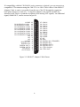
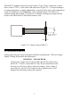
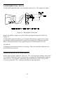
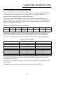
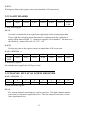
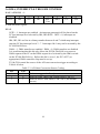
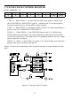
PC104-DAS16Jr/12
&
PC104-DAS16Jr/16
User’s Manual
Revision 4
August, 2001
MEGA-FIFO, the CIO prefix to data acquisition board model numbers, the PCM prefix to data
acquisition board model numbers, PCM-DAS08, PCM-D24C3, PCM-DAC02, PCM-COM422,
PCM-COM485, PCM-DMM, PCM-DAS16D/12, PCM-DAS16S/12, PCM-DAS16D/16,
PCM-DAS16S/16, PCI-DAS6402/16, Universal Library, InstaCal, Harsh Environment
Warranty and Measurement Computing Corporation are registered trademarks of Measurement
Computing Corporation.
IBM, PC, and PC/AT are trademarks of International Business Machines Corp. Windows is a
trademark of Microsoft Corp. All other trademarks are the property of their respective owners.
Information furnished by Measurement Computing Corp. is believed to be accurate and
reliable. However, no responsibility is assumed by Measurement Computing Corporation
neither for its use; nor for any infringements of patents or other rights of third parties, which
may result from its use. No license is granted by implication or otherwise under any patent or
copyrights of Measurement Computing Corporation.
All rights reserved. No part of this publication may be reproduced, stored in a retrieval system,
or transmitted, in any form by any means, electronic, mechanical, by photocopying, recording
or otherwise without the prior written permission of Measurement Computing Corporation.
Notice
Measurement Computing Corporation does not authorize any
Measurement Computing Corporation product for use in life support
systems and/or devices without the written approval of the President of
Measurement Computing Corporation Life support devices/systems are
devices or systems which, a) are intended for surgical implantation into
the body, or b) support or sustain life and whose failure to perform can
be reasonably expected to result in injury. Measurement Computing
Corp. products are not designed with the components required, and are
not subject to the testing required to ensure a level of reliability suitable
for the treatment and diagnosis of people.
(C) Copyright 2001 Measurement Computing Corporation.
HM PC104-DAS16Jr_##.lwp
Table of Contents
................................................1
1 INSTALLATION
1.1 SOFTWARE . . . . . . . . . . . . . . . . . . . . . . . . . . . . . . . . . . . . . . . . . . . . . . . . . . . 1
1.2 HARDWARE . . . . . . . . . . . . . . . . . . . . . . . . . . . . . . . . . . . . . . . . . . . . . . . . . . 1
1.3 BASE ADDRESS . . . . . . . . . . . . . . . . . . . . . . . . . . . . . . . . . . . . . . . . . . . . . . . 2
1.4 DMA LEVEL SELECT . . . . . . . . . . . . . . . . . . . . . . . . . . . . . . . . . . . . . . . . . . 3
1.5 1 OR 10 MHZ CRYSTAL OSCILLATOR JUMPER . . . . . . . . . . . . . . . . . . 3
1.6 8/16 CHANNEL SELECT . . . . . . . . . . . . . . . . . . . . . . . . . . . . . . . . . . . . . . . . 4
1.7 INSTALLING THE BOARD . . . . . . . . . . . . . . . . . . . . . . . . . . . . . . . . . . . . . 4
2 SIGNAL CONNECTIONS . . . . . . . . . . . . . . . . . . . . . . . . . . . . . . . . . . . . . . . . . . . 5
2.1 CONNECTOR DIAGRAM . . . . . . . . . . . . . . . . . . . . . . . . . . . . . . . . . . . . . . . 5
2.2 ANALOG INPUTS . . . . . . . . . . . . . . . . . . . . . . . . . . . . . . . . . . . . . . . . . . . . . 7
2.3 SINGLE-ENDED . . . . . . . . . . . . . . . . . . . . . . . . . . . . . . . . . . . . . . . . . . . . . . . 8
2.4 FLOATING DIFFERENTIAL . . . . . . . . . . . . . . . . . . . . . . . . . . . . . . . . . . . . . 8
2.5 DIFFERENTIAL INPUT . . . . . . . . . . . . . . . . . . . . . . . . . . . . . . . . . . . . . . . . 10
2.6 DIGITAL OUTPUTS & INPUTS . . . . . . . . . . . . . . . . . . . . . . . . . . . . . . . . . 10
3 REGISTER ARCHITECTURE . . . . . . . . . . . . . . . . . . . . . . . . . . . . . . . . . . . . . . 11
3.1 CONTROL & DATA REGISTERS . . . . . . . . . . . . . . . . . . . . . . . . . . . . . . . 11
3.2 A/D DATA & CHANNEL REGISTERS . . . . . . . . . . . . . . . . . . . . . . . . . . . 12
3.2.1 12-BIT BOARDS . . . . . . . . . . . . . . . . . . . . . . . . . . . . . . . . . . . . . . . . 12
3.2.2 16-BIT BOARDS . . . . . . . . . . . . . . . . . . . . . . . . . . . . . . . . . . . . . . . . 13
3.3 CHANNEL MUX SCAN LIMITS REGISTER . . . . . . . . . . . . . . . . . . . . . . 13
3.4 4-BIT DIGITAL I/O REGISTERS . . . . . . . . . . . . . . . . . . . . . . . . . . . . . . . . 14
3.5 STATUS REGISTER . . . . . . . . . . . . . . . . . . . . . . . . . . . . . . . . . . . . . . . . . . . 15
3.6 DMA, INTERRUPT & TRIGGER CONTROL . . . . . . . . . . . . . . . . . . . . . . 16
3.7 PACER CLOCK CONTROL REGISTER . . . . . . . . . . . . . . . . . . . . . . . . . . 17
3.8 ANALOG INPUT RANGE REGISTER . . . . . . . . . . . . . . . . . . . . . . . . . . . . 18
3.9 PACER CLOCK DATA & CONTROL REGISTERS . . . . . . . . . . . . . . . . . 18
3.10 ANALOG INPUTS . . . . . . . . . . . . . . . . . . . . . . . . . . . . . . . . . . . . . . . . . . . 19
3.11 DIGITAL INPUT & OUTPUT . . . . . . . . . . . . . . . . . . . . . . . . . . . . . . . . . . 20
. . . . . . . . . . . . . . . . . . . . . . . . . . . . . . . . . . . . . . . . . . . . . 21
4 SPECIFICATIONS
This page is blank.
1 INSTALLATION
1.1 SOFTWARE
Before you open your computer and install the board, install and run InstaCal™, the
installation, calibration and test utility included with your board. InstaCal™ will guide
you through switch and jumper settings for your board. Detailed information
regarding these settings can be found below. Refer to the Software Installation manual
for InstaCal™ installation instructions.
1.2 HARDWARE
The PC104-DAS16Jr/12 has one bank of switches, two single function switches and
one jumper block which must be set before installation of the board inside your
computer (Figure 1-1). The PC104-DAS16Jr/16 has one additional switch for
selecting unipolar or bipolar ranges (Figure 1-2).
8 or 16 CH A NN E L S ELE CT
SW ITCH
C RY STAL O S C.
FR EQ . S E LE C T
JUM P E R
1 or 10 M Hz
(1=U P)
A D D RE S S
D IP S W ITC H E S
300h D efault
P IN 1
(U N DE R)
D M A LE V E L
S E LE C T S W ITC H
Figure 1-1. PC104-DAS16Jr/12 Switch & Jumper Locations
1
B IP O L A R o r U N I P O L A R
S E L E C T S W IT C H (S 3 )
8 or 16 C H AN N EL SELEC T
S W IT C H (S 1 )
C R Y S TA L O S C .
FR EQ . SELEC T
JU M P E R (J1 )
1 or 10 M H z
(1 = D O W N )
ADDRESS
D IP S W IT C H E S
3 0 0 h D e fa u lt
P IN 1
(U N D E R )
D M A LEVEL SELEC T
S W IT C H (S 2 )
Figure 1-2. PC104-DAS16Jr/16 Switch and Jumper Locations
1.3 BASE ADDRESS
9
7
6
5
4
In the example shown in Figure 1-3, the
PC104-DAS16Jr/xx is set for base address
300h. See Figures 1-1 and 1-2 above for switch
orientations and locations on the boards.
8
The base address switches are set at the factory
to address 300h (768 decimal) as shown on
Figure 1-3. Unless there is already a board in
your system using this address, leave the
switches as they are set at the factory.
SW
A9
A8
A7
A6
A5
A4
HEX
200
100
80
40
20
10
Figure 1-3. Base Address Switches
2
1.4 DMA LEVEL SELECT
If using an XT PC there are only two DMA levels available and level 3 is probably
used by the hard disk controller. Set the DMA level switch to the level 1 position
(Figure 1-4). See Figure 1-1 or 1-2 for switch location.
If you have an AT or 386 type
computer the hard disk controller is
not at level 1 or 3 so either level may
be used.
There are other boards that use DMA
levels. Some network boards do and
so do some IEEE-488 interface
boards. If you have other boards in
your computer with DMA level
switches on them, make sure there are
no conflicts
Figure 1-4. DMA Level Select Switch
1.5 1 OR 10 MHZ CRYSTAL OSCILLATOR JUMPER
The 1/10 (1 or 10) MHz XTAL jumper selects the frequency of the source applied to
the on-board pacer. This pacer (counter 2) is used to pace the A/D start conversion
trigger (Figure 1-5). See Figure 1-1 or 1-2 for jumper location.
This jumper is on the board because the original DAS-16, designed in 1984, had a 1
MHz crystal. When MetraByte redesigned the DAS-16 and added the faster 10 MHz
crystal, a jumper was provided to maintain compatibility with older software.
The PC104-DAS16Jr/xx has the
jumper because the DAS-16 has the
jumper and some software requires
the jumper to be in the 1 MHz
position. However, some software
requires the 10 MHz position.
The PC104-DAS16Jr/xx is shipped
with the jumper in the 1 MHz
position. InstaCal allows you to
specify 1 or 10 MHz position in the
setup. See Figure 1-1 or 1-2 for
jumper location and orientation.
Note the difference in orientation in
Figures 1-1, 1-2, and 1-5.
10
1
MHz
J2
10
C IO -D A S 1 6 JR -1 2
MHz
1
C IO -D A S 1 6 JR -1 6
Figure 1-5. Frequency Select Jumpers
3
Older software may require the 1 MHz setting for this jumper. Use the 10MHz setting
for any new software development to get better resolution setting pacer frequencies.
1.6 8/16 CHANNEL SELECT
The PC104-DAS16Jr/xx can be
configured for eight differential
or 16 single-ended inputs. Using
differential inputs allows up to 10
volts of common mode (ground
loop) rejection and can be more
noise immune.
The PC104-DAS16Jr/xx comes
from the factory with the select
switch set for 8 differential inputs
as shown in Figure 1-6. Set it for
the number of inputs you desire.
See Figure 1-1 or 1-2 for switch
location.
Figure 1-6. Channel Quantity Select Switch
1.7 INSTALLING THE BOARD
Having configured the board’s switches and jumpers, it is now time to add the board
to the PC104 bus in the PC.
1.
Turn the power off.
2.
Remove any covers, etc. so you can get access to the PC104 bus. Please be
careful not to dislodge any of the cables installed on the boards in your
computer.
3.
Remove the retaining screws on the topmost PC104 card installed. Replace
these screws with the threaded standoffs provided.
4.
Push the PC104-DAS16Jr/xx board firmly down into the PC104 bus
connector. Secure it in place with the screws removed in the previous step.
4
2 SIGNAL CONNECTIONS
2.1 CONNECTOR DIAGRAM
The PC104-DAS16Jr/xx analog connector is a 40-pin in-line header connector (Figure
2-1). This connector accepts the C40FF-# cable which mates with the CIO-MINI40
screw terminal board.
NC
NC
CH0 HI
CH1 HI
CH2 HI
CH3 HI
CH4 HI
CH5 HI
CH6 HI
CH7 HI
LL G N D
LL G N D
NC
SSH
D IG ITA L IN 0
D IG ITA L IN 2
D IG ITA L O U T 0
D IG ITA L O U T 2
C TR 0 C LO C K
C TR 2 O U T
40
38
36
34
32
30
28
26
24
22
20
18
16
14
12
10
8
6
4
2
39
37
35
33
31
29
27
25
23
21
19
17
15
13
11
9
7
5
3
1
NC
LL G N D
C H 8 H IG H \C H 0 LO W
C H 9 H IG H \C H 1 LO W
C H 10 H IG H \C H 2 L O W
C H 11 H IG H \C H 3 LO W
C H 12 H IG H \C H 4 L O W
C H 13 H IG H \C H 5 L O W
C H 14 H IG H \C H 6 L O W
C H 15 H IG H \C H 7 L O W
NC
NC
NC
D IG ITA L G N D
D IG ITA L IN 1
D IG ITA L IN 3
D IG ITA L O U T 1
D IG ITA L O U T 3
C TR 0 O U T
+5 V P C B U S
Figure 2-1. PC104-DAS16Jr/xx Board Connector Pinout
NOTE: On both board versions, pin 1 is the bottom (closest to the board) left-hand
corner pin of the connector when the board is viewed edge - on from the connector
side with the components facing up.
5
If compatibility with the CIO-DAS16 series connector is desired, you can convert to a
compatible 37D connector using the C40-37F-# or C40-37M-# cables. If the BP40-37
Adapter Cable is used, is accessible from the rear of the PC through the expansion
back plate (Figures 2-2 and 2-3). Using these adapters, the signals available are
identical to the DAS-16 (with the exception of the missing D/A signals). An additional
signal, SS&H OUT, can be accessed at pin 26.
LLGND
CH 8 HIGH\CH 0 LOW
CH 9 HIGH\CH 1 LOW
CH 10 HIGH\CH 2 LOW
CH 11 HIGH\CH 3 LOW
CH 12 HIGH\CH 4 LOW
CH 13 HIGH\CH 5 LOW
CH 14 HIGH\CH 6 LOW
CH 15 HIGH\CH 7 LOW
NC
NC
NC
LLGND
DIGITAL IN 1
DIGITAL IN 3
DIGITAL OUT 1
DIGITAL OUT 3
CTR 0 OUT
+5V PC BUS
19
18
17
16
15
14
13
12
11
10
9
8
7
6
5
4
3
2
1
37
36
35
34
33
32
31
30
29
28
27
26
25
24
23
22
21
20
CH0 HI
CH1 HI
CH2 HI
CH3 HI
CH4 HI
CH5 HI
CH6 HI
CH7 HI
LLGND
LLGND
NC
SSH
DIGITAL IN 0 / TRIGGER
DIGITAL IN 2
DIGITAL OUT 0
DIGITAL OUT 2
CTR 0 CLOCK
CTR 2 OUT
Figure 2-2. BP40-37 Adapter Cable Pinout
6
The BP40-37 Adapter connector accepts female 37-pin, D-type connectors, such as
those on the C37FF-2, 2 foot cable with connectors (Figure 2-3). If frequent changes
to signal connections or signal conditioning is required, please refer to the information
on the CIO-MINI37, CIO-TERMINAL screw terminal board, CIO-EXP32, 32
channels analog MUX/AMP, CIO-SSH16, 16 channel simultaneous sample & hold
board or the ISO-RACK16 5B module interface rack.
B P 4 0-3 7
3 7 -p in c a b le, a s
C 37 F F -x, e tc.
P C 1 0 4-D A S 1 6 JR /x x
B a c k P la te
Figure 2-3. Cabling Using a BP40-37
2.2 ANALOG INPUTS
Analog inputs may be connected in three different configurations. These are Single
Ended, Floating Differential and Differential.
WARNING - PLEASE READ
Measure the voltage between the ground signal at the signal source
and the PC. If there is more than 10 volts, do not connect the board
because you will not be able to make any reading. If the voltage is
more than 30 volts, DO NOT connect to this signal because it will
damage the board and possibly the computer.
7
2.3 SINGLE-ENDED
A single-ended input is two wires connected to the board, a channel high (CH# HIGH)
and a Low Level Ground (LLGND). The LLGND signal must be the same ground the
PC is on. The CH# HIGH is the voltage signal source (Figure 2-4).
8
16
Figure 2-4. Single-Ended Input
2.4 FLOATING DIFFERENTIAL
A floating differential input is two wires from the signal source and a 10K ground
reference resistor installed at the input. The two signals from the signal source are
Signal High (CH# HIGH) and Signal Low (CH# LOW).
The reference resistor is connected between CH# LOW and LLGND pins.
8
A floating differential hookup is handy when the signal source is floating with respect
to ground, such as a battery, 4-20 mA transmitter or and the lead lengths are long or
subject to EMI interference (Figure 2-5).
Figure 2-5. Floating Source Differential Input
The floating differential input will reject up to 10V of EMI energy on the signal wires.
WARNING
Check it with a ohmmeter to determine that the signal source really
floating before risking the board and the PC!
9
2.5 DIFFERENTIAL INPUT
A differential signal has three wires from the signal source. The signals are Signal
Figure 2-6. Differential Connections
High (CH# HIGH), Signal Low (CH# LOW) and Signal Ground (LLGND). See
Figure 2-6.
A differential connection allows you to connect the board to a signal source with a
ground that is different than the PC ground, but less than 10V difference, and still
make a valid measurement of the signal between CH# HIGH and CH# LOW.
EXAMPLE:
A laboratory instrument with its own wall plug. There are sometimes differences in
wall GND between outlets.
2.6 DIGITAL OUTPUTS & INPUTS
All the digital outputs inputs are TTL level. TTL is an electronics industry term, short
for Transistor Transistor Logic, with describes a standard for digital signals which are
either at 0V or 5V (nominal). The binary logic inside the PC is all TTL or LSTTL
(Low power Schotky TTL). Both specifications are presented here.
10
3 REGISTER ARCHITECTURE
3.1 CONTROL & DATA REGISTERS
The PC104-DAS16Jr/xx is controlled and monitored by writing to and reading from
16 consecutive 8-bit I/O addresses. The first address, or BASE ADDRESS, is
determined by setting a bank of switches on the board.
Most often, register manipulation is best left to experienced programmers with a
specific need for low level control. If this is the case for you, use the information that
follows to write your own code. Otherwise, we strongly suggest you consider using
the Universal Library™ instead.
The register descriptions all follow the format:
7
A/D9
6
A/D10
5
A/D11
4
A/D12
LSB
3
CH8
2
CH4
1
CH2
0
CH1
The numbers along the top row are the bit positions within the 8-bit byte and the
numbers and symbols in the bottom row are the functions associated with that bit.
To write to or read from a register in decimal or HEX, the following weights apply:
Table 3-1. Bit Weights
BIT POSITION
0
1
2
3
4
5
6
7
DECIMAL VALUE
1
2
4
8
16
32
64
128
HEX VALUE
1
2
4
8
10
20
40
80
To write control or data to a register, the individual bits must be set to 0 or 1 then
combined to form a Byte.
The method of programming required to set/read bits from bytes is beyond the scope
of this manual.
In summary form, the registers and their function are listed on Table 3-2.
11
Table 3-2. Register Summary
ADDRESS
BASE
BASE + 1
BASE + 2
BASE + 3
BASE + 4
BASE + 5
BASE + 6
BASE + 7
BASE + 8
BASE + 9
BASE + 10
BASE + 11
BASE + 12
BASE + 13
BASE + 14
BASE + 15
READ FUNCTION
A/D Bits 9 to 12 (LSB) & Chan. #
A/D Bits 1 (MSB) to 8
Channel MUX Read
Digital 4 Bit Input
None
None
None
None
Status EOC, UNI/BIP etc.
DMA, Interrupt & Trigger Control
Pacer clock control register
Gain setting read-back
Counter 0 Data
CTR 1 Data - A/D Pacer Clock
CTR 2 Data- A/D Pacer Clock
None. No read back on 8254.
WRITE FUNCTION
Start A/D Conversion
None
Channel MUX Set
Digital 4 Bit Output
None
None
None
None
None
Set DMA, INT etc.
None
Gain control
Counter 0 Data
CTR 1 Data - A/D Pacer
CTR 2 Data - A/D Pacer
Pacer Clock Control (8254)
3.2 A/D DATA & CHANNEL REGISTERS
BASE ADDRESS:
3.2.1 12-BIT BOARDS
7
A/D9
6
A/D10
5
A/D11
4
A/D12
LSB
3
CH8
2
CH4
1
CH2
0
CH1
Read/write register.
READ
On read, it contains two types of data. The least significant four digits of the analog
input data and the channel number which the current data was taken from.
These four bits of analog input data must be combined with the eight bits of analog
input data in BASE + 1, forming a complete 12 bit number. The data is in the format
0 = minus full scale. 4095 = +FS.
The channel number is binary. The weights are shown in Table 3-1. If the current
channel were 5 then bits CH4 and CH1 would be high, CH8 and CH2 would be low.
12
WRITE
Writing any data to the register causes an immediate A/D conversion.
3.2.2 16-BIT BOARDS
7
A/D8
6
A/D9
5
A/D10
4
A/D11
3
A/D12
2
A/D13
1
A/D14
0
A/D15
LSB
A read/write register.
READ
On read, it contains the least significant eight digits of the Analog input data.
These eight bits of analog input data must be combined with the eight bits of
analog input data in BASE + 1, forming a complete 16 bit number. The data is in
the format 0 = minus full scale. 65,536 = +FS.
WRITE
Writing any data to the register causes an immediate A/D conversion.
BASE ADDRESS + 1
7
A/D0
MSB
6
A/D1
5
A/D2
4
A/D3
3
A/D4
2
A/D5
1
A/D6
0
A/D7
1
CH L2
0
CH L1
A Read-only register.
On read the most significant A/D byte is read.
3.3 CHANNEL MUX SCAN LIMITS REGISTER
BASE ADDRESS + 2
7
CH H8
6
CH H4
5
CH H2
4
CH H1
3
CH L8
2
CH L4
A read and write register.
READ
The current channel scan limits are read as one byte. The high channel number
scan limit is in the most significant 4 bits. The low channel scan limit is in the
least significant 4 bits.
13
WRITE
The channel scan limits desired are written as one byte. The high channel number
scan limit is in the most significant 4 bits. The low channel scan limit is in the
least significant 4 bits.
Bits 3-0 contain the starting channel number and bits 7-4 contain the ending channel
number. If you wanted to scan channels 1, 2, 3 in that order, do so by placing the 3 in
bits 7-4 and the 1 in bits 3-0.
NOTE
Every write to this register sets the current A/D channel MUX
setting to the number in bits 0-3. See BASE + 8.
3.4 4-BIT DIGITAL I/O REGISTERS
BASE ADDRESS + 3
7
0
6
0
5
0
4
0
3
DI3
2
DI2,
CTR 0
GATE
1
DI1
0
DI0,
TRIG
When read...
READ
The signals present at the inputs are read as one byte, the most significant 4 bits of
which are always zero. The pins 25 (digital input 0) and 24 (digital input 2) digital
inputs have two functions each.
The TRIG function of digital input 0 may be used to hold of the first sample of an
A/D set by holding it low (0V) until you are ready to take samples, which are then
paced by the 8254. It can also be used as the source of an external start conversion
pulse, synchronizing A/D conversions to some external event.
When written to..
7
X
6
X
5
X
4
X
3
DO3
2
DO2
1
DO1
0
DO0
WRITE
The upper four bits are ignored. The lower four bits are latched TTL outputs.
Once written, the state of the inputs cannot be read back because a read back
would read the separate digital input lines (see above).
14
3.5 STATUS REGISTER
BASE ADDRESS + 8
7
EOC
6
U/B
5
MUX
4
INT
3
CH8
2
CH4
1
CH2
0
CH1
A read mostly, one-function-write register.
READ
EOC = 1, the A/D converter is busy. EOC = 0, it is free.
U/B = 1, the amplifier is in Unipolar mode. U/B = 0, is bipolar.
MUX = 1, Channels are configured 16 single ended. MUX = 0, 8 differential.
INT = 1, an external pulse has been received. INT = 0, the flip-flop is ready to
receive a pulse..
There is a flip-flop on the TRIGGER input (pin 25) which will latch a pulse as short
as 200 nanoseconds. Once triggered, this flip-flop must be reset by a write to this
register. Your interrupts service routine must do this before another interrupt trigger
can be received.
CH8, CH4, CH2 & CH1 are a binary number between 0 and 15 indicating the channel
number that the MUX is currently set to and is valid only when EOC = 0. The
channel MUX increments shortly after EOC = 1 so may be in a state of transition
when EOC = 1. The binary weight of each bit is shown in the table above.
WRITE
A write of any data to this register resets the flip-flop on the pin 25 input and sets the
INT bit to 0.
15
3.6 DMA, INTERRUPT & TRIGGER CONTROL
BASE ADDRESS + 9
7
INTE
6
IR4
5
IR2
4
IR1
3
Don’t
Care
2
DMA
1
TS1
0
TS0
A read and write register.
READ
INTE = 1, Interrupts are enabled. An interrupt generated will be placed on the
PC bus interrupt level selected by IR4, IR2 & IR1. INTE = 0, interrupts are
disabled.
IR4, IR2, IR1 are bits in a binary number between 0 and 7 which map interrupts
onto the PC bus interrupt levels 2 - 7. Interrupts 0 & 1 may not be asserted by the
PC104-DAS16Jr/xx.
DMA = 1, DMA transfers are enabled. DMA = 0, DMA transfers are disabled.
It is worth noting that this bit only allows the PC104-DAS16Jr/xx to assert a
DMA request to the PC on the DMA request level selected by the DMA switch
on the PC104-DAS16Jr/xx. Before this bit is set to 1, the PC's 8237 (or
appropriate) DMA controller chip must be set up.
TS1 & TS0 control the source of the A/D start conversion trigger according to
Table 4-4 below.
TS1
0
1
1
Table 3-3. A/D Start Conversion Source Coding
TS0
X
Software triggered A/D only.
0
Start on rising TRIGGER (Digital input 0, Pin 25)
1
Start on Pacer Clock Pulse (CTR 2 OUT, no external
access)
16
3.7 PACER CLOCK CONTROL REGISTER
BASE ADDRESS + 10
7
X
6
X
5
X
4
X
3
X
2
X
1
CTR0
0
TRIG0
WRITE only
CTR0 = 1. When CTR0 = 1, an on-board 100 kHz clock signal is ANDed with
the COUNTER 0 CLOCK INPUT (pin 21). A high on pin 21 will allow pulses
from the on-board source into the 8254 Counter 0 input.
CTR0 = 0. When CTR0 = 0, the input to 8254 Counter 0 is entirely dependent on
pulses at pin 21, COUNTER 0 CLOCK INPUT.
TRIG0 = 1. When TRIG0 = 1, the TRIGGER input at pin 25 is ANDed with
TRIG0 which must be high for the pulses from the on-board pacer clock (8254)
to start A/D conversions. The input at pin 25 is pulled up and will always be high
unless pulled low externally.
TRIG0 = 0. When = 0, the GATEs of counter 1 & 2 are held high, preventing the
gating of the pacer externally from pin 25.
Figure 3-1 shows the relationship of this register to the pacer counters and associated
logic..
Figure 3-1. Pacing Control Counters
17
3.8 ANALOG INPUT RANGE REGISTER
BASE ADDRESS + 11
7
X
6
X
5
X
4
X
3
Range
2
Uni/Bip
1
G1
0
G0
Table 3-4. Input Range Codes PC104-DAS16Jr/12
RANGE
1
0
0
0
0
0
0
0
0
UNI/BIP
0
0
0
0
0
1
1
1
1
G1
0
0
0
1
1
0
0
1
1
G0
0
0
1
0
1
0
1
0
1
INPUT RANGE
±10V
±5V
±2.5V
±1.25V
±0.625V
0 to 10V
0 to 5V
0 to 2.5V
0 to 1.25V
DECIMAL
8
0
1
2
3
4
5
6
7
Table 3-5. Input Range Codes PC104-DAS16Jr/16
RANGE
0
0
0
0
0
0
0
0
UNI/BIP
0
0
0
0
1
1
1
1
G1
0
0
1
1
0
0
1
1
G0
0
1
0
1
0
1
0
1
INPUT RANGE
±10V
±5V
±2.5V
±1.25V
0 to 10V
0 to 5V
0 to 2.5V
0 to 1.25V
DECIMAL
0
1
2
3
4
5
6
7
A write to this register sets the analog input range for all 8/16 analog inputs. For the
PC104-DAS16Jr/12, range is programmable; the lower four bits set the analog input
range. For the PC104-DAS16Jr/16, the lower two bits set the range; the Uni/Bip bit is
set by hardware and the Range bit is not used. The upper four bits are not used for
either board. The current range is determined by reading this register.
3.9 PACER CLOCK DATA & CONTROL REGISTERS
8254 COUNTER 0 DATA
BASE ADDRESS + 12
7
D8
6
D7
5
D6
4
D5
3
D4
18
2
D3
1
D2
0
D1
8254 COUNTER 1 DATA
BASE ADDRESS + 13
7
D8
6
D7
30Dh, 781 decimal
5
D6
4
D5
3
D4
2
D3
1
D2
0
D1
3
D4
2
D3
1
D2
0
D1
8254 COUNTER 2 DATA
BASE ADDRESS + 14
7
D8
6
D7
30Eh, 782 decimal
5
D6
4
D5
Because each counter will count as high as 65,535, loading or reading the counter data
is a multi-step process. Refer to the 82C54 data sheet for details regarding its
programming. The data sheet is available at:
http://www.measurementcomputing.com/PDFmanuals/82C54.pdf
8254 COUNTER CONTROL
BASE ADDRESS + 15
7
D8
6
D7
30Fh, 783 decimal
5
D6
4
D5
3
D4
2
D3
1
D2
0
D1
This register controls the operation and loading/reading of the counters. Refer to the
82C54 data sheet for programming details.
3.10 ANALOG INPUTS
Analog signals connected to the analog inputs are first fed into the two HI-0508
analog multiplexers (MUXs). A MUX's function is to select one of the inputs and
connect that input to the MUX output. One of these MUX chips connects CH0-CH7
high inputs. The other connects CH0-CH7 Low input (differential input mode) or
CH8-CH15 High inputs (single ended mode) depending on the state of the channel
configuration switch marked 8/16.
From the output of the MUX, the analog signal is fed into a programmable differential
amplifier.
The A/D converter chip has an integral sample & hold circuit, greatly simplifying
design and improving signal integrity. The A/D converter is capable of sampling rates
to 330 kHz but the DMA transfer circuitry of the personal computer's 8-bit bus is
limited to a maximum synchronous transfer rate of less than the maximum A/D rate.
19
Therefore the maximum sampling rate of the PC104-DAS16Jr/xx is dependent on the
computer.
3.11 DIGITAL INPUT & OUTPUT
There are four bits of output only and four bits of input only on the analog connector.
From the original DAS-16 design these were the only eight bits of digital I/O.
20
4 SPECIFICATIONS
Power consumption
+5VDC quiescent
PC104-DAS16Jr/12
PC104-DAS16Jr/16
+ 5VDC Operating (A/D converting to FIFO)
PC104-DAS16Jr/12
PC104-DAS16Jr/16
140 mA typical, 230 mA max
145 mA typical, 205 mA max
250 mA typical, 375 mA max
235 mA typical, 350 mA max
Analog input section
A/D converter type
PC104-DAS16Jr/16
PC104-DAS16Jr/12
Resolution
PC104-DAS16Jr/12
PC104-DAS16Jr/16
Number of channels
AD7805
AD7800
12 bits
16 bits
8 differential or 16 single-ended,
switch-selectable
Input ranges
PC104-DAS16Jr/12
±10V, ±5V, ±2.5V, ±1.25V,
±0.625V, 0 to 10V, 0 to 5V, 0 to
2.5V, 0 to 1.25V fully
programmable
±10V, ±5V, ±2.5V, ±1.25V
programmable in Bipolar mode OR
0 to 10V, 0 to 5V, 0 to 2.5V, 0 to
1.25V programmable in Unipolar
mode
Unipolar/Bipolar switch-selectable
Programmable: internal counter,
external source (Din 0 / Trigger) or
software polled
External polled gate trigger (DIn 0)
PC104-DAS16Jr/16
Polarity
A/D Pacing
A/D Trigger sources
A/D Triggering Modes
Digital:
Gated pacer, software polled. (Gate
must be disabled by software after
trigger event.)
From 512 sample FIFO via
interrupt, DMA or software polled
Channel 1 or 3, switch-selectable
Programmable
Data transfer
DMA
DMA enable
21
A/D conversion time
PC104-DAS16Jr/12
PC104-DAS16Jr/16
Throughput
PC104-DAS16Jr/12
PC104-DAS16Jr/16
Accuracy
PC104-DAS16Jr/12
PC104-DAS16Jr/16
Integral Linearity error
PC104-DAS16Jr/12
PC104-DAS16Jr/16
Differential Linearity
No missing codes guaranteed
PC104-DAS16Jr/12
PC104-DAS16Jr/16
Gain drift (A/D specs)
PC104-DAS16Jr/12
PC104-DAS16Jr/16
Zero drift (A/D specs)
PC104-DAS16Jr/12
PC104-DAS16Jr/16
3.3 µs
10 µs
150 kHz
100 kHz
0.01% of reading, ±1LSB
0.003% of reading, ±1LSB
±1 LSB
±1.5 LSB (±3LSB on 1.25V ranges)
±1 LSB
12 bits
16 bits
±6 ppm/°C
±7 ppm/°C
±1 ppm/°C
±2 ppm/°C
Common Mode Range
CMRR @ 60 Hz
Input leakage current (@ 25 deg C)
Input impedance
Absolute maximum input voltage
±10V
70 dB
±20 nA
10 Mohms min
±35V
Digital I/O section
Digital type
Configuration
FPGA
Two ports, 4 bits each, 4 input and
4 output
0.8V max
2.0V min
0.32V max
3.86V min
−0.5V , +5.5V
Programmable: levels 2 to 7
Programmable
End-of-conversion, DMA terminal
count
Input low voltage
Input high voltage
Output low voltage (IOL = 4 mA)
Output high voltage (IOH = −4 mA)
Absolute maximum input voltage
Interrupts
Interrupt enable
Interrupt sources
22
Counter section
Counter type
Configuration
82C54
3 down-counters, 16 bits each
Counter 0 - Independent user counter
Source: Programmable (external or
100 kHz internal source)
Gate: Available at connector (DIn 2)
Output: Available at connector (Ctr 0
Out)
Counter 1 - ADC Pacer Lower Divider
Source: Jumper-selectable 1/10 MHz
Gate: Tied to Counter 2 gate, can be
program-enabled at user
connector (DIn 0 / Trigger).
Output: Chained to Counter 2 Clock.
Counter 2 - ADC Pacer Upper Divider
Source: Counter 1 Output.
Gate: Tied to Counter 1 gate,
programmable source.
Output: Programmable as ADC Pacer
clock, hardwired to user
connector (Ctr 2 Out)
Clock input frequency
High pulse width (clock input)
Low pulse width (clock input)
Gate width high
Gate width low
Input low voltage
Input high voltage
Output low voltage
Output high voltage
10 MHz max
30 ns min
50 ns min
50 ns min
50 ns min
0.8V max
2.0V min
0.4V max
3.0V min
Crystal oscillator
Frequency
Frequency accuracy
10 MHz
100 ppm
Environmental
Operating temperature range
Storage temperature range
Humidity
0 to 50°C
−40 to 100°C
0 to 90% non-condensing
23
For your notes.
24
For your notes.
25
For your notes.
26
EC Declaration of Conformity
We, Measurement Computing Corporation., declare under sole responsibility that the
product:
PC104-DAS16Jr/12
PC104-DAS16Jr/16
Part Number
Analog input boards for PC104 bus
Description
to which this declaration relates, meets the essential requirements, is in conformity
with, and CE marking has been applied according to the relevant EC Directives listed
below using the relevant section of the following EC standards and other normative
documents:
EU EMC Directive 89/336/EEC: Essential requirements relating to electromagnetic
compatibility.
EU 55022 Class B: Limits and methods of measurements of radio interference
characteristics of information technology equipment.
EN 50082-1: EC generic immunity requirements.
IEC 801-2: Electrostatic discharge requirements for industrial process measurement
and control equipment.
IEC 801-3: Radiated electromagnetic field requirements for industrial process
measurements and control equipment.
IEC 801-4: Electrically fast transients for industrial process measurement and control
equipment.
Carl Haapaoja, Director of Quality Assurance
Measurement Computing Corporation
16 Commerce Boulevard,
Middleboro, Massachusetts 02346
(508) 946-5100
Fax: (508) 946-9500
E-mail: [email protected]
www. measurementcomputing.com