1
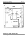
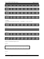
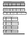
Elektronik für High End-Messtechnik (16.12.99 09:33 - 16.12.99 - 725_.doc) STR725 VME/VSB or VSB/VME Coupler Diese Dokumentation darf ohne Genehmigung der Fa. Bastian Technology GmbH & Co. KG weder ganz noch teilweise in irgendeiner Form reproduziert werden. 1998 Fa. Bastian Technology GmbH & Co. KG, Tangstedt All rights reserved. No part of this document may be reproduced, transmitted, transcribed, stored in a retrieval system, or translated into any form. 1998 Fa. Bastian Technology GmbH & Co. KG, Tangstedt Bastian Technology GmbH & Co. KG Bäckerbarg 6 D-22889 Tangstedt Phone: Fax: ++49 (0) 4109 55-0 ++49 (0) 4109 55-133 E-mail: [email protected] [email protected] Internet: http://www.batech.de Project: STR725 VME/VSB Coupler page 2 / V 1.21 Titel.............................. : VME/VSB Coupler Project .......................... : STR725 Author .......................... : T.H./T.E./OGK Version ......................... : 1.21 First issue ..................... : Last modification ......... : Released on .................. : March 1993 November 1998 Status ............................ : Filename....................... : 725_Nov98.doc Serial number : .... Released by .................. : Bastian Technology GmbH & Co. KG Bäckerbarg 6 D-22889 Tangstedt / Germany Phone: ++49 (0)4109 55 -0 Fax: ++49 (0)4109 55 -133 E-mail: [email protected] [email protected] Internet: http//www.batech.de Bastian Technology GmbH & Co. KG Print: 16.12.99 Project: STR725 VME/VSB Coupler page 3 / V 1.21 CONTENTS 1 STR725 INTRODUCTION ................................................................................ 4 2 HARDWARE COMPONENTS .......................................................................... 5 3 JUMPER FUNCTION AND JUMPER SETTINGS ............................................ 6 4 LEDS ................................................................................................................ 9 5 VSB-SLAVE/VME-MASTER MODE................................................................. 9 5.1 VSB-Slave/VME-Master mode LCA Design ........................................................................................ 9 6 7 VME-SLAVE 32 BIT/VSB-MASTER 32 BIT MODE ....................................... 11 6.1 Selecting the design ........................................................................................................................ 11 6.2 Selecting VME-Base address......................................................................................................... 12 6.3 Operation........................................................................................................................................ 12 6.4 Example 1 ....................................................................................................................................... 12 6.5 Startup ............................................................................................................................................ 13 6.6 LED’s............................................................................................................................................... 13 VME-SLAVE 16 BIT/VSB-MASTER 32 BIT MODE ....................................... 13 7.1 Selecting the Design ....................................................................................................................... 13 7.2 Selecting the VME-Base address .................................................................................................. 13 7.3 Operation........................................................................................................................................ 13 7.4 Example 2 ....................................................................................................................................... 14 7.5 Startup ............................................................................................................................................ 15 7.6 LED’s............................................................................................................................................... 15 Bastian Technology GmbH & Co. KG Print: 16.12.99 Project: STR725 VME/VSB Coupler page 4 / V 1.21 1 INTRODUCTION The STR725 is a versatile Interface module between the VSB and the VMEbus. The used configuration (EPROM, Jumper) defines the interfacing mode (VME-Slave/VSB-Master Mode or VSB-Slave/VME-Master Mode). Depending on the jumpered configuration this VME module uses the connectors P1 and/or P2. All VSB lines, using connector P2, and nearly all extended VME-lines (A32,D32), using connectors P1 and P2, are linked through the specified drivers to STR725-Logic. The buffered protocol-lines of the VSBbus and the VMEbus and the control lines of the address/data drivers are in connection with the programmable logic (LCA, Logic Cell Array). The EPROM configures this LCA-logic at starting-up time. It is possible to store 64 different LCA-designs in one EPROM. The required LCA-design can be selected by jumper setting. The module can work either in VME-Slave/VSB-Master mode (RDY_VSB-LCA Design) or in VSBSlave/VME-Master mode (RDY_VME-LCA Design). The STR725 can be prepared by software (LCA) for a multitude of interface tasks, and so it is a "wizard" among the interfaces. Only a few possibilities of designing for the VSB-VME mode can be listed here: - In Uni-Master mode in a VME crate arbitration in the VME crate is not necessary. - In VSB-Blocktransfer mode the VME address can be automatically incremented. - Timing adaptation on a slave without VME-Standard is possible - In Read mode the LCA logic can activate the Read cycle before it is demanded by the VSB (prefetching). - ... Bastian Technology GmbH & Co. KG Print: 16.12.99 Project: STR725 VME/VSB Coupler page 5 / V 1.21 2 HARDWARE COMPONENTS Block Diagram: 3 JUMPER FUNCTION AND JUMPER SETTINGS Bastian Technology GmbH & Co. KG Print: 16.12.99 Project: STR725 VME/VSB Coupler page 6 / V 1.21 JUMPER FUNCTION J1 J2 J3 J4 J5 J6 J7 J8 J9 = = = = = = = = = Address selection: Selection Address bits 31-24 Address selection: Enable Address bits 31-24 Address selection: Selection Address bits 23-16 Address selection: Enable Address bits 23-16 Selection of VME Requester Level VME Arbiter Type and Enable/Disable VME System Controller VME IACKIN/IACKOUT Daisy Chain Driver VSB Arbitration Daisy-Chain (only VSB-Master Mode) Selection of LCA-Design JUMPER SETTING J1/J3 If a Jumper is inserted in this array the selected address bit will be used for address decoding. J2/J4 Jumpers in the array J2/J4 define the level of the selected address bits for a valid address window. (Open Jumper positions on J1/J3 have to be open also on J2/J4) Jumper J1: Positions 1-16 Address bit 31 2-15 30 3-14 29 4-13 28 5-12 27 6-11 26 7-10 25 8-9 24 2-15 30 3-14 29 4-13 28 5-12 27 6-11 26 7-10 25 8-9 24 2-15 22 3-14 21 4-13 20 5-12 19 6-11 18 7-10 17 8-9 16 2-15 22 3-14 21 4-13 20 5-12 19 6-11 18 7-10 17 8-9 16 open: not selected close: selected Jumper J2: Positions 1-16 decoded bit 31 open: decoded as "1" close: decoded as "0" Jumper J3: Positions 1-16 Address bit 23 open: not selected close: selected Jumper J4: Positions 1-16 decoded bit 23 open: decoded as "1" close: decoded as "0" 1.Example: selected address bits are only A25,A24,A23; Crate address : 1 (/A25, /A24, A23) Jumper J1: Bastian Technology GmbH & Co. KG Print: 16.12.99 Project: STR725 VME/VSB Coupler page 7 / V 1.21 Positions 1-16 Jumper no 2-15 No 3-14 no 4-13 no 5-12 no 6-11 no 7-10 yes 8-9 yes Jumper J2: Positions Jumper 1-16 no 2-15 No 3-14 no 4-13 no 5-12 no 6-11 no 7-10 yes 8-9 yes Jumper J3: Positions Jumper 1-16 yes 2-15 No 3-14 no 4-13 no 5-12 no 6-11 no 7-10 no 8-9 no Jumper J4: Positions Jumper 1-16 no 2-15 No 3-14 no 4-13 no 5-12 no 6-11 no 7-10 no 8-9 no 2.Example: selected address bits are only A25,A24,A23; Crate address : 4 ( A25, /A24, /A23) Jumper J1: Positions Jumper 1-16 no 2-15 No 3-14 no 4-13 no 5-12 no 6-11 no 7-10 yes 8-9 yes Jumper J2: Positions Jumper 1-16 no 2-15 No 3-14 no 4-13 no 5-12 no 6-11 no 7-10 no 8-9 yes Jumper J3: Positions Jumper 1-16 yes 2-15 No 3-14 no 4-13 no 5-12 no 6-11 no 7-10 no 8-9 no Jumper J4: Positions Jumper 1-16 yes 2-15 No 3-14 no 4-13 no 5-12 no 6-11 no 7-10 no 8-9 no Jumper J5: VME Master Requester Level Level 3: 20 O | O 1 11 O O O O-- O O O O O-- O O | O O | O O O | O O 10 Level 2: 20 Bastian Technology GmbH & Co. KG 11 Print: 16.12.99 Project: STR725 VME/VSB Coupler O O 1 O | O O O O O O | O page 8 / V 1.21 O-| O-- O O O O O O O | O 10 Level 1: 20 O O | O O 1 O O O | O O O O | O O O O-| O-- O O 11 O O 10 Level 0: 20 O O 1 O O O | O O | O O O O | O O | O O O 11 O-O-10 O O Jumper J6: VME Arbiter Type and Enable/Disable VME System Controller Position 1-4 : Requester Modus open: ROR (Release on Request) closed: RWD (Release when done) Position 2-3 : VME System Controller open: Disabled closed: Enabled Jumper J7: VME IACKIN/IACKOUT Daisy Chain Driver Position 1-2 : closed if STR725 is not a VME System Controller Position 2-3 : closed if STR725 is a VME System Controller 4 LED’S O RDY-VSB (green) : indicates the VSB-Slave/VME-Master mode Bastian Technology GmbH & Co. KG Print: 16.12.99 Project: STR725 VME/VSB Coupler O RDY-VME (green) O O O I-SEL/CONF (yellow) : indicates selection and configuration VSB-ACT (red) : indicates own activities on the VSB-side VME-ACT (red) : indicates own activities on the VME-side O VME-ENSYS (green) : indicates that VME-System controller is enabled O O USER1 (red) USER2 (red) page 9 / V 1.21 : indicates the VME-Slave/VSB-Master mode : user definable : user definable During configuration of the LCAs the LED I-SEL/CONF is on and the both LED’s RDY-VSB and RDY-VME are off. After configuration one of the LED’s RDY-VSB and RDY-VME is on and in case of VME-master/VSB-slave the LED I-SEL/CONF is on when selecting the STR725. 5 VSB-SLAVE/VME-MASTER MODE 5.1 VSB-SLAVE/VME-MASTER MODE LCA DESIGN All Jumpers of J9 have to be inserted (1.Design). The address bits 25,24,23 form the Crate address (Jumpers J1,J2,J3,J4). Addressing Bits 25,24,23 --> Crate Address Bit 22 0 0 0 0 1 1 1 1 Bit 21 0 0 1 1 0 0 1 1 Bit 20 0 1 0 1 0 1 0 1 Function VME Short Non-Privileged Data Access ( AM = 29 ) VME Short Supervisor Data Access ( AM = 2D ) VME Standard Non-Privileged Data Access ( AM = 39 ) VME Standard Supervisor Data Access ( AM = 3D ) VME Extended Non-Privileged Data Access ( AM = 09 ) VME Extended Supervisor Data Access ( AM = 0D ) used internal AM-Register (only 1. VME-Cycle) STR725 internal addressing Internal Addresses Offset $2 $2 $4 $6 $6 $8 $C $E R/W W R W W R R R R Function write internal VME Offset-address register (Bits 31-20) read internal VME Offset-address register and address Register (Bits 31-0) write internal SIZE- and AM-Register (Bit 9-0) write internal IRQ-Enable-Register (Bit 31-24) read internal IRQ-Enable-Register (Bit 31-24) Version Register read VME IRQs (Bit 31-24) generate VME-IRQ-Ackn. Cycle SIZE/AM Register Bastian Technology GmbH & Co. KG Print: 16.12.99 Project: STR725 VME/VSB Coupler Bit 10 Adress increment disable Bit 5 Bit 4 AM5 page 10 / V 1.21 Bit 9 Led User2 Bit 8 LED User1 Bit 7 SIZE1 Bit 6 SIZE0 Bit 3 Bit 2 Bit 1 Bit 0 AM3 AM2 AM1 AM0 Bits 15-8 b2 B2 B2 Bits 7-0 b3 B3 B3 AM4 VSB-Slave / VME-Master Register Convention Table: Bus VSB-Bus (32) VME-Standard-Bus (16) VME-Extended-Bus (32) Bits 31-24 b0 Bits 23-16 b1 B0 B1 VSB-Size: Bit SIZE 1 0 1 0 Bit SIZE 0 0 0 1 Size of Data Transfer Longword (32) Word (16) Byte (8) Write Data into SIZE- and AM-Register $0 $80 $40 Data Transfer (only aligned transfer allowed): VSB Byte Transfer (VME-Standard 16 Bit): VSB A1 0 0 1 1 A0 0 1 0 1 VME DS0 DS1 H L L H H L L H LWORD x x x x b0 B2 x x x b1 x B3 x x b2 x x B2 x b3 x x x B3 b2 B0 x B2 x b3 x B1 x B3 b2 x B2 b3 x B3 b2 B0 B2 b3 B1 B3 VSB Byte Transfer (VME-Extended 32 Bit): VSB A1 0 0 1 1 A0 0 1 0 1 VME DS0 DS1 H L L H H L L H LWORD H H H H b0 x x x x b1 x x x x VSB Word Transfer (VME-Standard 16 Bit): VSB A1 0 1 VME A0 DS0 DS1 =0 L L =0 L L LWORD b0 x B2 x x b1 B3 x VSB Word Transfer (VME-Extended 32 Bit): VSB A1 0 1 VME A0 DS0 DS1 =0 L L =0 L L LWORD b0 H x H x Bastian Technology GmbH & Co. KG b1 x x Print: 16.12.99 Project: STR725 VME/VSB Coupler page 11 / V 1.21 VSB Longword Transfer (VME-Standard 16 Bit): (one VSB-Cycle ⇒ two VME-Cycles) VSB A1 =0 A0 =0 VME DS0 DS1 L L LWORD b0 b1 x B2(1) B3(1) b2 B2(2) b3 B3(2) b2 B2 b3 B3 (1) : 1.Cycle with A1=0 (2) : 2.Cylce with A1=1 VSB Longword Transfer (VME-Extended 32 Bit): VSB VME A1 A0 DS0 DS1 LWORD b0 b1 =0 =0 L L L B0 B1 6 VME-SLAVE 32 BIT/VSB-MASTER 32 BIT MODE On the VSB side no arbitration is generated to get bus mastership (single master). Restrictions: This mode requires a special chip set of Xilinx LCAs. The two Xilinx devices should be as: XC3030-100 and the EPROM on the board should be labeled as STR725-201. 6.1 SELECTING THE DESIGN In this mode on VME and VSB-side only aligned 32-bit transfers are allowed. For this design only the jumper areas J1...J4, J7 and J9 are relevant. The jumper configuration of J9 for using this design is shown here: 1-16 2-15 3-14 4-13 5-12 6-11 7-10 8-9 set set set set set set set set Jumper setting J9 In this mode only extended 32-Bit VME transfers incl. blocktransfers from and to the STR725 are allowed. 6.2 SELECTING VME-BASE ADDRESS For adjusting the base address of the VME-slave refer to chapter 3 (only jumper J1 to J4). Jumper J6 should be open and at J7 position 1-2 should be closed. 6.3 OPERATION Bastian Technology GmbH & Co. KG Print: 16.12.99 Project: STR725 VME/VSB Coupler page 12 / V 1.21 The VME addresses A1..A19 are directly mapped into the VSB address range. The upper VSB address bits A20..A31 are settable in an address offset register. To write to the offset register the following VME address is necessary: VME base address + (A23 = 1) = Offset Register Writing an address to the offset register, the data bits D20..D31 represent the upper VSB address. An access to the module via VME generates VSB cycles with following addresses: VME base address + offset Register D20..D31 = VSB address The VSB address offset register cannot be read back. Note: STR725 is shipped with address for offset register: $500 0000 and base address ist $ 400 0000. 6.4 EXAMPLE 1 An example in 68xxx assembler which uses $400 0000 as selected VME baseaddress. The VME CPU accesses the STR725 directly: move.l move.l STR725 #$4000000,a0 #$5000000,a1 VME baseaddress STR725 VSB offsetregister move.l #$f0000000,d0 (A24="1") VSB address to be accessed move.l #$3000,a2 move.b #$20,d2 internal memory address on VME CPU loop counter d0,(a1) set VSB offset move.l (a2)+,(a0)+ access to VSB subi.b tst.b #1,d2 d2 decrement counter end of write loop ? * define VSB offset address ********** move.l * write to VSB *********************** WR_LOOP beq WR_LOOP 6.5 STARTUP After power on the module is doing it’s configuration and the LED I-SEL/CONF is on for a few seconds. When configured this LED turns off and the LED VME should illuminate to indicate that the board is able to operate now. 6.6 LEDS Bastian Technology GmbH & Co. KG Print: 16.12.99 Project: STR725 VME/VSB Coupler page 13 / V 1.21 On the front panel the LED User 1 is illuminated, when data is written to the offset register. The LED User 2 is illuminated when data is written to or read from VSB. 7 VME-SLAVE 16 BIT/VSB-MASTER 32 BIT MODE On the VSB side no arbitration is generated to get bus mastership (single master). 7.1 SELECTING THE DESIGN In this mode on VME-side the slave-interface can be accessed only by 16-bit transfers in VMEstandard-mode (allowed address modifiers are $39, $3A, $3D, $3E). On VSB-side the masterinterface reads/writes only aligned 32-bit. To generate one VSB-cycle it is necessary to access the VME-slave with two 16-bit cycles. For this design only the jumper areas J3, J4, J7 and J9 are relevant. The jumper-configuration of J9 for using this design is shown here: 1-16 2-15 3-14 4-13 5-12 6-11 7-10 8-9 Set unset set set set set set set Jumper setting J9 7.2 SELECTING VME-BASE ADDRESS For adjusting the base address of the VME-slave refer to chapter 3 (only jumpers J3 and J4). The jumper areas J1 and J2 should be left open when working in A24 address-space, they will be used only in A32 mode. Only the jumper position 4-13 on J1 and J2 has to be open. Jumper J6 should be open and at J7 position 1-2 should be closed. Bastian Technology GmbH & Co. KG Print: 16.12.99 Project: STR725 VME/VSB Coupler page 14 / V 1.21 7.3 OPERATION The VME addresses A1..A19 are directly mapped into the VSB address range. The upper VSB address bits A20..A31 are settable in an address offset register. To access the offset register, only one 16 bit cycle is necessary. The flow of VME/VSB-cycles appears as follows: - Write to STR725 via VME: In the first 16-bit VME-cycle the address (A19..A1) and the data word (high word) are latched on the board. At this point there is no action on VSB-side. In the second 16-bit VME-cycle the data (low word) is stored on the module and the latched VMEaddress from the first VME-cycle is combined with the value in the offset-register and written to VSB-side as a valid address. After the address-phase is finished both stored data words (high and low word) are transferred to VSB. The second VME-cycle "wraps" the VSB-action in the sense that the VME-cycle will be terminated when the complete VSB-access has done. - Read from STR725 via VME: In the first VME-cycle the contents of the VSB address-offset-register is appended to the VMEaddress and written to VSB. A 32-bit read-action is done on VSB-side, the low data word (D15..D0) is stored on the board and the high data word (D31..D16) is presented on the VME data lines. After the VSB-cycle is terminated this first VME-cycle is acknowledged. The second VME-access runs without VSB-action. The stored low data word (D15..D0) is fetched. To write to the offset register the following VME address is used : VME base address + (A20 = 1) = Offset Register Writing an address to the offset register, the data bits D20..D31 represent the upper VSB address. The bit positions D16..D19 are don’t care they are part of the present VME-address. Address-offset-register: Bit positions 16 bit within offset register: 31 30 29 28 27 12 bit VSB address-offset: 31 30 29 28 27 26 25 24 23 22 21 20 26 25 24 23 22 21 20 19 18 17 don’t care: X X X 16 X An access to the module via VME generates VSB cycles with following addresses: Accessed VME address A1..A19 + offset register D20..D31 = VSB address The VSB address offset register cannot be read back. Bastian Technology GmbH & Co. KG Print: 16.12.99 Project: STR725 VME/VSB Coupler page 15 / V 1.21 7.4 EXAMPLE 2 An example in 68xxx assembler which uses $400 0000 as selected VME baseaddress. The VME CPU accesses via STR725[1] and a VDB connection a second STR725[2] in a second VME rack. STR725[1] is the VME-slave/VSB-master and STR725[2] acts as VSB-slave/VME-master. STR725[2] is jumpered to crate address "1" => A25 = 0, A24 = 0, A23 = 1 (see example 1 in the main manual VME/VSB Coupler) move.l #$400 0000,a0 VME baseaddress STR725[1] move.l STR725[1] #$500 0000,a1 VSB offset register (A24="1") move.l #$F0 0002,d0 internal offset register move.l #$90 0000,d1 VME destination address to be accessed in the second VME move.l #$C0 0000,d2 declare access mode for second VME rack in STR725[2]: VME extended non priv. data move.l #$3000,a2 move.b #$20,d2 internal memory source address on VME CPU loop counter STR725[2] rack acc. * define VME offset address on STR725[2] ********** move.l d0,(a1) move.l d1,(a0) write internal offset address of STR725[2] into offset register of STR725[1] configure STR725[2] with dest. address in second VME rack * define VME cycles in second VME rack on STR725[2] ********** move.l d2,(a1) write VME access mode for STR725[2] into offset register of STR725[1] * end of configuration STR725[1] + [2] ************** * write data block to second VME crate *********************** WR_LOOP move.l (a2)+,(a0)+ access to VSB subi.b tst.b #1,d2 d2 decrement counter end of write loop ? beq WR_LOOP Bastian Technology GmbH & Co. KG Print: 16.12.99 Project: STR725 VME/VSB Coupler page 16 / V 1.21 7.5 STARTUP After power on the module is doing it’s configuration and the LED I-SEL/CONF is on for a few seconds. When configured this LED turns off and the LED VME should illuminate to indicate that the board is able to operate now. 7.6 LED’S On the front panel the LED User 1 is illuminated, when data is written to the address offset register. The LED User 2 is illuminated when data is written to or read from VSB. Änderungen / Changes Lfd.Nr. 1. 2. 3. 4. 5. 6. 7. 8. 9. Version 1.21 Datum 17.11.1998 Name OGK Bastian Technology GmbH & Co. KG Bemerkungen Print: 16.12.99