1
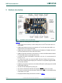
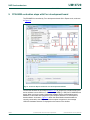
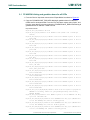
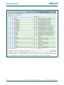
UM10729
PCA9955A demonstration board OM13483
Rev. 1 — 23 July 2014
User manual
Document information
Info
Content
Keywords
Fm+ I2C-bus, PCA9955A, RGB and White LEDs, 16-channel x 8-bit PWMs
Abstract
The OM13483 is an add-on to 9-pin connector of the NXP I2C demo board
2005-1 or Fm+ I2C-bus development board. This daughter board makes it
easy to test and design with the PCA9955A, a 16-channel Fast-mode Plus
(Fm+) 57 mA constant current and outputs allow up to 20 V for LED supply.
This demo board, along with the Win-I2CUSB Lite GUI (PC based),
provides an easy to use evaluation platform.
UM10729
NXP Semiconductors
PCA9955A demonstration board OM13483
Revision history
Rev
Date
Description
1.0
20140723
User manual; initial release.
Contact information
For more information, please visit: http://www.nxp.com
For sales office addresses, please send an email to: [email protected]
UM10729
User manual
All information provided in this document is subject to legal disclaimers.
Rev. 1 — 23 July 2014
© NXP Semiconductors N.V. 2014. All rights reserved.
2 of 24
UM10729
NXP Semiconductors
PCA9955A demonstration board OM13483
1. Introduction
The PCA9955A evaluation board features LEDs for color mixing, blinking and dimming
demonstrations. A graphical interface allows the user to explore the different functions of
the driver easily. The board can be connected in series with other I2C demo-boards to
create an evaluation system.
The IC communicates to the host via the industry standard I2C-bus/SMBus port. The
evaluation software runs under Microsoft Windows PC platform.
2. Features
• A complete evaluation platform for the PCA9955A 16-channel Fm+ I2C-bus constant
current LED driver
•
•
•
•
•
Easy to use GUI-based software demonstrates the capabilities of the PCA9955A
On-board four white and four RGB LEDs for visual experience
Convenient test points for easy scope measurements and signal access
USB interface to the host PC
No external power supply required
3. Getting started
3.1 Assumptions
Familiarity with the I2C-bus is helpful, but not required.
3.2 Static handling requirements
CAUTION
This device is sensitive to ElectroStatic Discharge (ESD). Therefore care should be taken
during transport and handling. You must use a ground strap or touch the PC case or other
grounded source before unpacking or handling the hardware.
3.3 Minimum system requirements
•
•
•
•
PC Pentium 60 processor (or equivalent), 8 MB RAM, 10 MB of hard drive space
One USB port (either 2.0 or 1.1 compatible)
Windows 98SE, ME, 2000, XP, or Vista
I2C demonstration board 2005-1 (OM6275) or Win-I2CUSB board (from
www.demoboard.com)
3.4 Power requirements
The NXP demonstration board I2C 2005-1 and OM13483 hardware obtain power from the
PC USB port. Care should be taken not to exceed the USB port current capabilities.
UM10729
User manual
All information provided in this document is subject to legal disclaimers.
Rev. 1 — 23 July 2014
© NXP Semiconductors N.V. 2014. All rights reserved.
3 of 24
UM10729
NXP Semiconductors
PCA9955A demonstration board OM13483
4. Installation
4.1 I2C demo board 2005-1 and Win-I2CUSB Lite software
The OM13483 is a daughter card to the OM6275 I2C demo board 2005-1. You may
download the Win-I2CUSB Lite Software, the OM6275 user manual UM10206, and find
ordering information at the NXP web site www.nxp.com/demoboard/OM6275.html.
The OM13483 is a daughter card to the OM13260 Fm+ I2C-bus development board,
which is part of the Fm+ development board kit (OM13320). You may download the
software, user manual, and find ordering information at the NXP web site:
www.nxp.com/demoboard/OM13320.html#documentation.
The Win-I2CUSB Lite software from The Boardshop runs on Windows 98SE, ME, 2000,
and XP and is compatible with any PC hardware having a minimum of a Pentium
processor and a USB port. The software allows the user to select one of the I2C-bus
devices on the board from a menu. It also provides a Universal mode (I2C Expert mode) to
allow users to create their own I2C-bus commands with the same I2C-bus devices.
4.2 OM13483 connection to I2C demo board 2005-1
The I2C demo board 2005-1 should be disconnected from your PC before mounting the
OM13483 board on to it. The OM13483 board has a 9-pin female connector (CON2) that
connects to the JP1 male connector on the I2C demo board 2005-1 as shown in Figure 1.
With both boards facing you, and with USB connector on the right-hand side as shown in
Figure 1, connect the OM13483 board to the I2C demo board 2005-1 before connecting
the USB cable. Once the board is connected, connect the USB cable and start the
Win-I2CUSB Lite software. You are now ready to evaluate the PCA9955A.
UM10729
User manual
All information provided in this document is subject to legal disclaimers.
Rev. 1 — 23 July 2014
© NXP Semiconductors N.V. 2014. All rights reserved.
4 of 24
UM10729
NXP Semiconductors
PCA9955A demonstration board OM13483
Fig 1.
UM10729
User manual
PCA9955A demo board (OM13483) mounting to the I2C demo board 2005-1
(OM6275)
All information provided in this document is subject to legal disclaimers.
Rev. 1 — 23 July 2014
© NXP Semiconductors N.V. 2014. All rights reserved.
5 of 24
UM10729
NXP Semiconductors
PCA9955A demonstration board OM13483
4.3 OM13483 connection to Fm+ I2C bus development board
The OM13260 Fm+ I2C bus development board should be disconnected from your PC
before mounting the OM13483 board onto it. The OM13483 board has a 9-pin female
connector (CON2) that connects to the CN2 male connector on the bridge board
(OM13399) as shown in Figure 2.
PCA9955A
demo board
(OM13483)
9-pin connector
Select Bus 1
to drive PCA9955A
Bridge board
(OM13399)
14-pin connector
Fm+ development board
(OM13260)
To PC
USB port
aaa-014227
Fig 2.
PCA9955A demo board (OM13483) mounting to the Fm+ development board (OM13260)
UM10729
User manual
All information provided in this document is subject to legal disclaimers.
Rev. 1 — 23 July 2014
© NXP Semiconductors N.V. 2014. All rights reserved.
6 of 24
UM10729
NXP Semiconductors
PCA9955A demonstration board OM13483
4.4 OM13483 connection to Win-I2CUSB hardware adapter board
The Win-I2CUSB board should be disconnected from your PC before connecting the
OM13483 board on to it. The OM13483 board has a 14-pin male connector (CON4) that
connects to the 14-pin male connector (J1) on the Win-I2CUSB board as shown in
Figure 3.
Connect the OM13483 board to the Win-I2CUSB board before connecting the USB cable.
Once the board is connected, connect the USB cable and start the Win-I2CUSB Lite
software. You are now ready to evaluate the PCA9955A.
Fig 3.
UM10729
User manual
PCA9955A demo board (OM13483) connecting to the Win-I2CUSB board
All information provided in this document is subject to legal disclaimers.
Rev. 1 — 23 July 2014
© NXP Semiconductors N.V. 2014. All rights reserved.
7 of 24
UM10729
NXP Semiconductors
PCA9955A demonstration board OM13483
5. Hardware description
Fig 4.
PCA9955A demo board (OM13483)
Figure 4 shows the following items on the hardware:
• CON1 (9-pin male connector) is used to daisy-chain to next I2C-bus slave device or
demo board.
• CON2 (9-pin female connector) is connected to JP1 on I2C demo board 2005-1 as
master device to drive this demo board.
• CON3 (5-pin male connector) is connected to the PCU9669 or PCA9665 mini board
as I2C-bus master device to drive this demo board.
• CON4 (14-pin male connector) is connected to J1 on Win-I2CUSB hardware board as
I2C-bus master device to drive this demo board.
• J1 selects VDD power for PCA9955A, connected 1-2 for VDD = 5 V and connected 2-3
for VDD = 3.3 V.
• J7, J9 and J10 to select one of the five (GND, Pull-down, Floating, Pull-up and VDD)
input levels to address inputs AD[0:2] for a maximum of 125 possible programmable
I2C-bus slave address.
• LED[0:15] 16-channel output to drive four White LEDs (WHT_LED[1:4]) and four RGB
LEDs (RGB_LED[1:4]).
• TP2 and TP3 are GND pins for probing use.
• TP1 can be connected as external reset signal to RESET pin when J6 is open.
• TP4 can be connected as external output enable signal to OE pin for blinking/dimming
control when J11 is open.
• All jumpers default setting and function as shown in Table 1.
UM10729
User manual
All information provided in this document is subject to legal disclaimers.
Rev. 1 — 23 July 2014
© NXP Semiconductors N.V. 2014. All rights reserved.
8 of 24
UM10729
NXP Semiconductors
PCA9955A demonstration board OM13483
Table 1.
Jumper settings for test and evaluation
Jumper
Default setting Comment
J1
(3-pin)
1-2
(VDD = +5 V)
This jumper is used to select VDD for PCU/PCA9955A.
J2
(3 × 2-pin)
1-2
(REXT = 1 kΩ,
57 mA at max.)
This 3 × 2 jumper is used to select REXT (pin 1) value for PCU/PCA9955A.
J3
(2-pin)
Short
Short: external 1.1 kΩ pull-up resistor for SDA on PCA9955A.
Open: no external pull-up resistor for SDA on PCA9955A.
Remark: No external pull-up resistor required for PCU9955A.
J4
(2-pin)
Short
Short: external 1.1 kΩ pull-up resistor for SCL on PCA9955A.
Open: no external pull-up resistor for SCL on PCA9955A.
Remark: No external pull-up resistor required for PCU9955A.
J5
(2-pin)
Short
Short: connect VDD (pin 28) to PCU/PCA9955A.
Open: connect current meter to measure the IDD on PCU/PCA9955A.
J6
(2-pin)
Open
Short: force RESET (pin 25) to GND.
Open: 10 kΩ pull-up RESET (pin 25) to VDD.
J7
(4 × 2-pin)
7-8[1]
This 4 × 2 jumper is used to select quinary input value for AD0 (pin 2).
J8
(3-pin)
1-2
J9
(5 × 2-pin)
7-8[1]
J10
(5 × 2-pin)
7-8[1]
J11
(2-pin)
Short
UM10729
User manual
1-2: select +5 V
2-3: select +3.3 V
1-2: select REXT = 1 kΩ and maximum output current is 57.3 mA
3-4: select REXT = 1.5 kΩ and maximum output current is 38.25 mA
5-6: select REXT = 2 kΩ and maximum output current is 28.6 mA
Open: floating
1-2: select VDD
3-4: select pull-up with 31.6 kΩ
5-6: select pull-down with 34.8 kΩ
7-8: select GND
This jumper is used to select bus mode.
1-2: select normal I2C or SPI addressable bus mode
2-3: select SPI daisy-chain bus mode
This 5 × 2 jumper is used to select quinary input value for AD1 (pin 3).
Open: floating
1-2: select VDD
3-4: select pull-up with 31.6 kΩ
5-6: select pull-down with 34.8 kΩ
7-8: select GND
9-10: SDO (Serial Data Out) for SPI addressable mode or last slave device in SPI
daisy-chain
This 5 × 2 jumper is used to select quinary input value for AD2 (pin 4).
Open: floating
1-2: select VDD
3-4: select pull-up with 31.6 kΩ
5-6: select pull-down with 34.8 kΩ
7-8: select GND
9-10: CSN (Chip Select) for SPI bus mode
Short: force OE (pin 5) to GND, to enable LEDs output.
Open: 10 kΩ pull-up OE (pin 5) to VDD when applying external clock for blinking/dimming on
TP4 (test point).
All information provided in this document is subject to legal disclaimers.
Rev. 1 — 23 July 2014
© NXP Semiconductors N.V. 2014. All rights reserved.
9 of 24
UM10729
NXP Semiconductors
PCA9955A demonstration board OM13483
Table 1.
Jumper settings for test and evaluation …continued
Jumper
Default setting Comment
J12, J16,
J19, J22
(2-pin)
Short
J13
(3-pin)
This jumper is used to select LED supply voltage.
1-2
(VLED = +3.3 V)
1-2: select +3.3 V for all LEDs supply voltage.
2-3: select +5 V for all LEDs supply voltage.
Open (no jumper): select external voltage from J20 (≤ +20 V) and J24 (GND)
J14, J18
(2-pin)
Open
These jumpers are used to open the WHT_LED1 or RGB_LED1 J12 to control White LED,
J16 to control Red LED, J19 to control Green LED, J22 to control Blue LED.
Open: connected the current meter to measure one of the LEDs output current or open one
of the LEDs outputs for detecting an LED open condition in one of EFLAGn registers.
Short: normal operation for WHT_LED1 and RGB_LED1.
These jumpers are used to merge the LED[0:2] outputs together for driving higher LED
current.
Open: normal operation for the LED[0:2].
Short: When short J14/J18 and open J16/J19 to combine LED[0:2] outputs to drive LED0.
When short J14 only and open J16 to combine LED[0:1] outputs to drive LED0.
J15, J17,
J21, J23
(2-pin)
Open
These jumpers are used to short the WHT_LED1 or RGB_LED1 J15 to control White LED,
J17 to control Red LED, J23 to control Green LED, J21 to control Blue LED.
J20
(2-pin)
+20 V input
External ≤ +20 V input for LEDs supply voltage. The J13 is open to supply this ≤ +20 V
voltage to all LEDs.
J24
(2-pin)
GND
External GND input for LEDs supply voltage.
J25, J27,
J29, J31
(2-pin)
Short
These jumpers are used to open the WHT_LED4 or RGB_LED4.
Open: normal operation for WHT_LED1 and RGB_LED1.
Short: to short one of the LEDs output for detecting an LED short condition in one of
EFLAGn registers.
J25 to control White LED, J27 to control Red LED, J29 to control Green LED, J31 to control
Blue LED.
Open: connect current meter to measure one of the LEDs output current or open one of the
LEDs outputs for detecting an LED open condition in one of EFLAGn registers.
Short: normal operation for WHT_LED4 and RGB_LED4.
J26, J28,
J30, J32
(2-pin)
Open
These jumpers are used to short the WHT_LED4 or RGB_LED4.
J26 to control White LED, J28 to control Red LED, J32 to control Green LED, J30 to control
Blue LED.
Open: normal operation for WHT_LED4 and RGB_LED4.
Short: to one of the LEDs for detecting an LED short condition in one of EFLAGn registers.
CON1
9-pin male
connector
This 9-pin connector is used to daisy-chain to next I2C-bus slave device or demo board.
CON2
9-pin female
connector
This 9-pin connector is used to connect to Fm+ I2C development board or I2C 2005-1
evaluation board as master device to drive this demo board.
CON3
5-pin male
connector
This 5-pin connector is used to connect to the PCU9669 or PCA9665 mini board as I2C-bus
master device to drive this demo board.
CON4
14-pin header
This 14-pin header is used to connect to Win-I2CUSB hardware board as I2C-bus master
device to drive this demo board.
TP1
Test Point 1
This TP1 is used to drive RESET input pin 25 from external when J6 is open.
TP2, TP3
Test Point 2/3
These two test points are GND for probe ground connection.
TP4
Test Point 4
This TP4 is used to drive OE input pin 5 from external when J11 is open.
[1]
Default PCU/PCA9955A slave address is 0x02h (AD[2:0] = GND).
UM10729
User manual
All information provided in this document is subject to legal disclaimers.
Rev. 1 — 23 July 2014
© NXP Semiconductors N.V. 2014. All rights reserved.
10 of 24
xxxx xxxxxxxxxxxxxxxxxxxxxxxxxxxxxx x xxxxxxxxxxxxxx xxxxxxxxxx xxx xxxxxx xxxxxxxxxxxxxxxxxxxxxxx xxxxxxxxxxxxxxxxxxxxxx
xxxxx xxxxxx xx xxxxxxxxxxxxxxxxxxxxxxxxxxxxx xxxxxxxxxxxxxxxxxxxxxx xxxxxxxxxxx xxxxxxx xxxxxxxxxxxxxxxxxxx
xxxxxxxxxxxxxxxx xxxxxxxxxxxxxx xxxxxx xx xxxxxxxxxxxxxxxxxxxxxxxxxxxxxxxx xxxxxxxxxxxxxxxxxxxxxxxx xxxxxxx
xxxxxxxxxxxxxxxxxxxxxxxxxxxxxxxxxxxxxxxxxxxxxx xxxxxxxxxxx xxxxx x x
3
2
1
(SPI_SCLK) SCL-Filter
J2
R2
(Io_LED_MAX = 38.25 mA)
1.5 kΩ
+5 V
2
4
6
+5 V
R3
10 kΩ
R4
1.1 kΩ
9-pin female connector
to/from I2C 2005-1 board
R5
1.1 kΩ
L1
H1206N101R-10
CON2
+5 V
R14
0Ω
CON3
R15
31.6 kΩ
R16
34.8 kΩ
R17
0Ω
+24 V
+5 V
SDA-Filter
C5
SCL-Filter
10 μF
GND
C6
HEADER 5x2
(short 9-10 for SPI addressable mode
or last slave device in SPI daisy-chain)
10 μF
R19
31.6 kΩ
R20
34.8 kΩ
R21
0Ω
1
3
5
7
9
2
LED15
LED14
LED13
LED12
C3
0.1 μF
LED11
LED10
LED9
LED8
1
HEADER 7x2/8M
2
L2
BLM18BD471SN1
PCA9955A demo board schematic (part A)
GND VDD
I/O1
I/O2
4
VDD_IN
3
C7
0.01 μF
GND
TP3
PRTR5V0U2AX
SDA-filter
L3
BLM18BD471SN1
SCL-filter
SCL
(470 Ω at 100 MHz)
Fig 5.
2
VDD_IN
4
SCL
6 GND
8
SDA
10
12
14
+5 V
aaa-013943
UM10729
11 of 24
© NXP Semiconductors N.V. 2014. All rights reserved.
10 kΩ
1-2: normal I2C or SPI addressable
2-3: SPI daisy-chain
U2
TP4
1-2: LED output control
Open −> Output disabled
Short −> Output enabled
(Pins [5:9] to/from
the 2nd SPI slave
PCA9955A
demo board)
14-pin header connector to/from
Win-I2CUSB I2C master to drive
PCA9955A demo board
SDA
1
J8
AD1
SDA
(Green LED for
VDD indicator)
LED[0:15]
Ext /OE input
J11
9-pin female
D1
LTST-C170GKT
CON4
GND 1
1
2
R9
1 kΩ
1
3
5
7
GND 9
11
13
+3.3 V
Quinary input pad connection to AD[2:0]
Open −> floating
1-2 −> VDD
3-4 −> pull-up
5-6 −> pull-down
7-8 −> GND
HEADER 5x2
(short 9-10 for SPI mode)
R22
C4
4.7 μF
1-2 −> force reset
Open −> normal
SPI_CSN
TP2
open to measure
the U1 current
1
J6
C1
10 μF
VDD_IN
2
2
1
2
close to VDD pin
J5
PCA9955A demonstration board OM13483
0Ω
SDA-Filter
SCL-Filter
0Ω
0Ω
LED[0:15]
AD2
2
4
6
8
10
J10
R18
J4 open (no PU)
for PCU9955A
1
R7
R8
Thermal pad 5.5 x 2.2 mm
add thermal vias 5 x 2
0.28 mm diameter with 1 mm pitch
with the barrel plated to about 1.0 ounce copper
SPI_SDO
5-pin Male
GND
LED4
LED5
LED6
LED7
AD1
2
4
6
8
10
J9
1
3
5
7
9
J3
1
2
+3.3 V
3
4
C2
SCL (SPI_SCLK) 5
10 μF
GND
6
SPI_SDI 7
SPI_SDO
8
9
SPI_CSN
1
5-pin male connector to/from
bus controller PCU9669 mini board
to drive PCA/PCU9955A
VDD
REXT
AD0
SDA/USDA
AD1
SCL/USCL
RESET
AD2
OE
VSS
LED0
LED15
LED1
LED14
LED2
LED13
LED3
LED12
VSS
VSS
LED4
LED11
LED5
LED10
LED6
LED9
LED7
LED8
RESET
28
27
26
25
24
23
22
21
20
19
18
17
16
15
AVR-M1608C080M1
VDD_IN
U1
PCU/PCA9955A
1
2
3
4
5
6
7
8
9
10
11
12
13
14
VARISTOR
Rev. 1 — 23 July 2014
All information provided in this document is subject to legal disclaimers.
SPI_SDO
SPI_CSN
(Pins [5:9] to/from the
SPI master device)
1
(SPI_SDI) SDA-Filter
JUMPER 3x2
(Io_LED_MAX = 28.6 mA)
2 kΩ LED max. ouput current setting:
1-2 −> Rext = 1 kΩ, 57.3 mA = 225 μA × 255
3-4 −> Rext = 1.5 kΩ, 38.25 mA = 150 μA × 255
5-6 −> Rext = 2 kΩ, 28.6 mA = 112.5 μA × 255
AD0
AD0
J7
AD1
R10
0Ω
1
2
AD2
3
4
OE
31.6 kΩ
R11
5
6
LED0
7
8
LED1
34.8 kΩ
R12
LED2
JUMPER 4x2
0Ω
R13
LED3
2
R6
9-pin Male
1
2
3
4
5
1
3
5
+3.3 V
+3.3 V
TP1
1
+3.3 V
Ext /RST input
(Io_LED_MAX = 57.3 mA)
1 kΩ
3
+5 V
1
R1
CON1
1
2
3
4
5
6
7
8
9
NXP Semiconductors
9-pin male connector to/from
2nd PCA9955A demo board
6. Schematic
UM10729
User manual
J1
PCU9955A (OM13484) and PCA9955A (OM13483)
16-ch 57 mA/20 V constant current LED driver Test/Demo Board
xxxx xxxxxxxxxxxxxxxxxxxxxxxxxxxxxx x xxxxxxxxxxxxxx xxxxxxxxxx xxx xxxxxx xxxxxxxxxxxxxxxxxxxxxxx xxxxxxxxxxxxxxxxxxxxxx
xxxxx xxxxxx xx xxxxxxxxxxxxxxxxxxxxxxxxxxxxx xxxxxxxxxxxxxxxxxxxxxx xxxxxxxxxxx xxxxxxx xxxxxxxxxxxxxxxxxxx
xxxxxxxxxxxxxxxx xxxxxxxxxxxxxx xxxxxx xx xxxxxxxxxxxxxxxxxxxxxxxxxxxxxxxx xxxxxxxxxxxxxxxxxxxxxxxx xxxxxxx
xxxxxxxxxxxxxxxxxxxxxxxxxxxxxxxxxxxxxxxxxxxxxx xxxxxxxxxxx xxxxx x x
NXP Semiconductors
UM10729
User manual
4 white and 4 RGB LEDs connect to PCU/PCA9955A 16-channel outputs
(The LEDs supply voltage can be selected either internal +3.3 V/+5 V or external up to +20 V.)
WHT-LED1
LW-E67C
R23
1
LED1
J14
2
1
LED2
R25
LED1 + LED2
0Ω
J18
2
LED1 open test and
output current measurement
1 J19 2
RGB_LED1
LRTB_G6SF
(R)
LED2 open test and
output current measurement
R26
A1
(G) C2
A2
C1
C3 (B)
A3
1 J17 2
LED1 short test
1 J21 2
1
2
J23
External voltage input for LED supply
(Less or equal 20 V input and J13 is open)
LED2 short test
2
LED3 open test
and output current measurement
+3.3 V
+5 V
HEADER 2
1 J22 2
0Ω
+5 V
LED voltage select:
OPEN: use external voltage
1-2: internal +3.3 V
2-3: internal +5 V
J20
LED3 short test
1
LED3
+3.3 V
3
1 J15 2
LED0 short test
1 J16 2
0Ω
1
2
LED0 open test and
output current measurement
LED0 + LED1
R24
J13
1 J12 2
0Ω
RGB1
LED0
J24
1
2
LED4
0Ω
LED5
R28
0Ω
HEADER 2
Notes:
VF = 3.2 V for White LED
VF = 2.1 V for Red LED
VF = 3.2 V for Green LED
VF = 3.2 V for Blue LED
LED6
R29
0Ω
A1
(G) C2
A2
LED7
LED[0:15]
LED[0:15]
R30
RGB2
RGB_LED2
LRTB_G6SF
(R)
C1
C3 (B)
A3
Open/Short test only available for
first four channels LED[0:3] and
last four channels LEd[12:15]
0Ω
These serial resistors (R23-R38) can change to
non-zero value for voltage switch PCA/PCU9655A
devices to adjust LED output current.
LED8
R31
0Ω
LED9
R32
0Ω
LED10
R33
0Ω
WHT-LED3
LW-E67C
C8
10 μF
RGB_LED3
LRTB_G6SF
A1
(G) C2
A2
LED11
R34
C1
C3 (B)
A3
0Ω
WHT-LED4
LW-E67C
R35
0Ω
LED13
R36
0Ω
R37
0Ω
RGB_LED4
LRTB_G6SF
LED13 open test and
output current measurement
1 J29 2
(R)
LED15
R38
A1
(G) C2
LED14 open test and
output current measurement
A2
C1
C3 (B)
A3
1 J28 2
LED13 short test
1 J30 2
LED15 short test
1 J31 2
0Ω
1
LED15 open test and
output current measurement
C13 C14 C15 C16 C17 C18 C19 C20 C21 C22 C23 C24
0.1 nF 0.1 nF 0.1 nF 0.1 nF 0.1 nF 0.1 nF 0.1 nF 0.1 nF 0.1 nF 0.1 nF 0.1 nF 0.1 nF
LED14 short test
2
J32
C9
C10 C11
C12
0.1 nF 0.1 nF 0.1 nF 0.1 nF
aaa-013944
Fig 6.
PCA9955A demo board schematic (part B)
UM10729
12 of 24
© NXP Semiconductors N.V. 2014. All rights reserved.
LED14
1 J26 2
LED12 short test
1 J27 2
RGB4
LED12
1 J25 2
LED12 open test and
output current measurement
PCA9955A demonstration board OM13483
(R)
RGB3
Rev. 1 — 23 July 2014
All information provided in this document is subject to legal disclaimers.
WHT-LED2
LW-E67C
R27
UM10729
NXP Semiconductors
PCA9955A demonstration board OM13483
7. OM13483 demonstration board main components
Table 2.
OM13483 demo board main components
Device
Description
PCA9955ATW
0x02h for I2C demo board
16-channel Fm+ I2C-bus
57 mA / 20 V constant current (default setting)
LED driver
Address/LED
Location
U1
PRTR5V0U2AX
ESD protection diode
-
U2
LW-E67C
White LED
4 white LEDs
WHT_LED[1:4]
LRTB_G6SG
RGB LED
4 RGB LEDs
RGB_LED[1:4]
LTST-C170GKT
Green LED for PCA9955A
power supply either 3.3 V or
5 V indicator
1 green LED
D1
8. PCA9955A evaluation steps
The PCA9955A is controlled by Win-I2CUSB GUI in Expert mode, as shown in Figure 7.
Fig 7.
Drop-down menu selection for Expert mode
Connect the hardware as described in Section 4. All jumpers are in default setting and
device address is set to 0x02 on J7, J9 and J10 (set AD[0:2] = GND) for PCA9955A
demo board. When you have correctly installed the software and the demonstration board
hardware is connected and recognized by the computer, start the Win-I2CUSB Lite
UM10729
User manual
All information provided in this document is subject to legal disclaimers.
Rev. 1 — 23 July 2014
© NXP Semiconductors N.V. 2014. All rights reserved.
13 of 24
UM10729
NXP Semiconductors
PCA9955A demonstration board OM13483
software. As shown in Figure 7, when the demonstration board hardware is correctly
connected to the USB port and the computer recognizes it, the message ‘Hardware
Detected’ is displayed on the bottom of the window.
Switched 3.3 V and 5.0 V power supplies are controlled through the ‘Options’ menu or by
double-clicking the 3.3 V or 5.0 V symbols on the bottom of the window. Power supplies
are disabled by default and must be enabled before using the I2C-bus devices on the
board. I2C-bus frequency is controlled through the ‘Options’ menu or by double-clicking
the frequency symbol on the bottom of the window.
8.1 PCA9955A blinking demo for all White and RGB LEDs
1. From the ‘Device’ drop-down menus select ‘Universal Modes’, and from the
subsequent drop-down menu select ‘Expert Mode’ as shown in Figure 7.
2. Copy the ‘PCA9955A WHT_RGB LEDs blinking demo i2c address = 0x02h’ text file
as shown below. From the ‘File’ drop-down menus select ‘Open’, and from the
‘open data file’ window select the ‘PCA9955A WHT_RGB LEDs blinking demo
i2c address = 0x02h’ text file.
Expert Mode Data File
00,Write,Yes,0,06,Comments: SW reset
02,Write,Yes,0,45,80,Comments: write IREFALL to
channel)
02,Write,Yes,500,82,01,01,01,01,Comments: start
white LEDs
02,Write,Yes,700,82,04,04,04,04,Comments: start
red LEDs
02,Write,Yes,500,82,01,01,01,01,Comments: start
white LEDs
02,Write,Yes,700,82,10,10,10,10,Comments: start
green LEDs
02,Write,Yes,500,82,01,01,01,01,Comments: start
white LEDs
02,Write,Yes,700,82,40,40,40,40,Comments: start
blue LEDs
02,Write,Yes,300,82,01,00,00,00,Comments: start
white LEDs
02,Write,Yes,300,82,00,05,00,00,Comments: start
white, red LEDs
02,Write,Yes,300,82,00,00,51,00,Comments: start
white, Blue_Green LEDs
02,Write,Yes,300,82,00,00,00,55,Comments: start
white and RGB LEDs
02,Write,Yes,400,82,40,01,04,10,Comments: start
white and RGB LEDs
02,Write,Yes,400,82,10,40,01,04,Comments: start
white and RGB LEDs
02,Write,Yes,400,82,04,10,40,01,Comments: start
white and RGB LEDs
02,Write,Yes,400,82,01,40,10,04,Comments: start
white and RGB LEDs
UM10729
User manual
All information provided in this document is subject to legal disclaimers.
Rev. 1 — 23 July 2014
80h (225 uA x 128 = 28.8 mA per
write LEDOUTx register to turn on
write LEDOUTx register to turn on
write LEDOUTx register to turn on
write LEDOUTx register to turn on
write LEDOUTx register to turn on
write LEDOUTx register to turn on
write LEDOUTx register to turn on
write LEDOUTx register to turn on
write LEDOUTx register to turn on
write LEDOUTx register to turn on
write LEDOUTx register to turn on
write LEDOUTx register to turn on
write LEDOUTx register to turn on
write LEDOUTx register to turn on
© NXP Semiconductors N.V. 2014. All rights reserved.
14 of 24
UM10729
NXP Semiconductors
PCA9955A demonstration board OM13483
02,Write,Yes,0,81,21,FF,FF,FF,FF,Comments: start write 01h register to program the
DMBLNK=1 for blinking, LDRx=11 for group dimming/blinking controlled by
GRPPWM, GRPFREQ
02,Write,Yes,0,44,C0,Comments: write PWMALL register to set the PWMx=C0h 75% duty
cycles for individual LED
02,Write,Yes,2000,86,40,00,Comments: write GRPPWM=40h for duty cycle (ON/OFF ratio
in 25%) and GRPFREQ= 00h (67 ms for blinking period)
02,Write,Yes,2000,86,80,01,Comments: write GRPPWM=80h for duty cycle (ON/OFF ratio
in 50%) and GRPFREQ= 02h (131 ms for blinking period)
02,Write,Yes,2000,86,A0,02,Comments: write GRPPWM=C0h for duty cycle (ON/OFF ratio
in 62.5%) and GRPFREQ= 04h (196 ms for blinking period)
02,Write,Yes,2000,86,C0,03,Comments: write GRPPWM=FFh for duty cycle (ON/OFF ratio
in 75%) and GRPFREQ= 06h (262 ms for blinking period)
00,Write,Yes,0,06,Comments: SW reset
Sequence:01,02,03,04,05,06,07,08,09,10,11,12,13,14,15,16,17,18,19,20,21,22,23
3. After opening the ‘PCA9955A WHT_RGB LEDs blinking demo i2c address = 0x02h’
text file, the Win-I2CUSB GUI in Expert mode screen will be displayed as shown in
Figure 8.
4. Click the ‘Send All’ button. All the valid messages on the screen is sent in order of the
row number (Msg #). The action is performed one time.
Fig 8.
UM10729
User manual
Message data in Expert mode to demonstrate all White and RGB LEDs for
blinking
All information provided in this document is subject to legal disclaimers.
Rev. 1 — 23 July 2014
© NXP Semiconductors N.V. 2014. All rights reserved.
15 of 24
UM10729
NXP Semiconductors
PCA9955A demonstration board OM13483
8.2 Test of LED open or short error detection
The PCA9955A can detect an LED open or short condition at its open-drain LED outputs.
Users recognize these faults by reading the status of a pair of error bits (ERRx) in error
flag registers (EFLAGn) for each channel.
The user can poll the ERROR status bit (bit 6 in MODE2 register) to check if there is a
fault condition in any of the 16 channels. The EFLAGn registers can then be read to
determine which channels are at fault and the type of fault in those channels.
1. Copy the ‘PCA9955A Open or Short test’ text file as shown below. From the ‘File’
drop-down menus select ‘Open’, and from the ‘open data file’ window select the
‘PCA9955A Open or Short test’ text file.
Expert Mode Data File
00,Write,Yes,5,06,Comments: software reset
02,Write,Yes,0,98,80,80,Comments: set current to 50% of max in IREF0/IREF1
02,Write,Yes,50,02,05,Comments: set LED0 and LED1 are fully ON
02,Write,Yes,1,01,11,Comments: Clear all error status bits in EFLAGn registers by
writing bit4=1 in MODE2
02,Read,Yes,0,01,Comments: read ERROR status (bit6) in MODE2
02,Write,Yes,0,46,Comments: set EFLAG0 register address
02,Read,Yes,0,00,Comments: Read EFLAG0 status (bit1/0 for LED 0 and bit 3/2 for
LED1 error status)
02,Write,Yes,1,01,11,Comments: Clear all error status bits in EFLAGn registers by
writing bit4=1 in MODE2
02,Write,Yes,0,98,00,00,Comments: set output current to zero in IREF0/IREF1
Sequence:01,02,03,04,05,06,07,08,09
2. After opening the ‘PCA9955A Open or Short test’ text file, the Win-I2CUSB GUI in
Expert mode screen will be displayed as shown in Figure 9.
3. Click the ‘Send All’ button. All the valid messages on the screen is sent in order of the
row number (Msg #). The action is performed one time.
4. To verify the read data on message line 5 for ERROR status and line 7 for EFLAG
status.
5. To open the J12 and J16 for open-circuit test on LED0 and LED1, repeat steps 3 and
4 to find the error report in message line 5 and line 7.
6. To short the J15 and J17 for short-circuit test on LED0 and LED1, repeat steps 3 and
4 to find the error report in message line 5 and line 7.
UM10729
User manual
All information provided in this document is subject to legal disclaimers.
Rev. 1 — 23 July 2014
© NXP Semiconductors N.V. 2014. All rights reserved.
16 of 24
UM10729
NXP Semiconductors
PCA9955A demonstration board OM13483
Fig 9.
UM10729
User manual
Example of Open or Short-circuit test for LED0 and LED1
All information provided in this document is subject to legal disclaimers.
Rev. 1 — 23 July 2014
© NXP Semiconductors N.V. 2014. All rights reserved.
17 of 24
UM10729
NXP Semiconductors
PCA9955A demonstration board OM13483
9. PCA9955A evaluation steps with Fm+ development board
The PCA9955A is controlled by Fm+ development board GUI in Expert mode, as shown
in Figure 10.
Fig 10. Select the Expert mode from Fm+ development board GUI
Connect the hardware as described in Section 4.3. All jumpers are in default setting and
device address is set to 0x02 on J7, J9 and J10 (set AD[0:2] = GND) for PCA9955A demo
board. When you have correctly installed the software and the demonstration board
hardware is connected and recognized by the computer, start the Fm+ development
board software. As shown in Figure 10, when the demonstration board hardware is
correctly connected to the USB port and the computer recognizes it, the message
‘USB-I2C Hardware Detected’ is displayed on the bottom of the window.
UM10729
User manual
All information provided in this document is subject to legal disclaimers.
Rev. 1 — 23 July 2014
© NXP Semiconductors N.V. 2014. All rights reserved.
18 of 24
UM10729
NXP Semiconductors
PCA9955A demonstration board OM13483
9.1 PCA9955A blinking and gradation demo for all LEDs
1. From the ‘Device’ drop-down menus select ‘Expert Modes’ as shown in Figure 10.
2. Copy the ‘PCA9955A WHT_RGB LEDs blinking & gradation demo i2c address =
0x02h’ text file as shown below. From the ‘File’ drop-down menus select ‘Open’, and
from the ‘open data file’ window to select the ‘PCA9955A WHT_RGB LEDs blinking &
gradation demo i2c address = 0x02h’ text file.
Expert Mode Data File
00,Write,Yes,0,06,Comments: SW reset
02,Write,Yes,0,45,80,Comments: write IREFALL to 80h (225uA x 128 = 28.8mA per
channel)
02,Write,Yes,500,82,01,01,01,01,Comments: start write LEDOUTx register to turn on
white LEDs
02,Write,Yes,700,82,04,04,04,04,Comments: start write LEDOUTx register to turn on
red LEDs
02,Write,Yes,500,82,01,01,01,01,Comments: start write LEDOUTx register to turn on
white LEDs
02,Write,Yes,700,82,10,10,10,10,Comments: start write LEDOUTx register to turn on
green LEDs
02,Write,Yes,500,82,01,01,01,01,Comments: start write LEDOUTx register to turn on
white LEDs
02,Write,Yes,700,82,40,40,40,40,Comments: start write LEDOUTx register to turn on
blue LEDs
02,Write,Yes,300,82,01,00,00,00,Comments: start write LEDOUTx register to turn on
white LEDs
02,Write,Yes,300,82,00,05,00,00,Comments: start write LEDOUTx register to turn on
white, red LEDs
02,Write,Yes,300,82,00,00,51,00,Comments: start write LEDOUTx register to turn on
white, Blue_Green LEDs
02,Write,Yes,300,82,00,00,00,55,Comments: start write LEDOUTx register to turn on
white and RGB LEDs
02,Write,Yes,400,82,40,01,04,10,Comments: start write LEDOUTx register to turn on
white and RGB LEDs
02,Write,Yes,400,82,10,40,01,04,Comments: start write LEDOUTx register to turn on
white and RGB LEDs
02,Write,Yes,400,82,04,10,40,01,Comments: start write LEDOUTx register to turn on
white and RGB LEDs
02,Write,Yes,400,82,01,40,10,04,Comments: start write LEDOUTx register to turn on
white and RGB LEDs
02,Write,Yes,0,81,21,FF,FF,FF,FF,Comments: start write 01h register to program the
DMBLNK=1 for blinking, LDRx=11 for group dimming/blinking controlled by
GRPPWM, GRPFREQ
02,Write,Yes,0,44,C0,Comments: write PWMALL register to set the PWMx=C0h 75% duty
cycles for individual LED
02,Write,Yes,2000,86,40,00,Comments: write GRPPWM=40h for duty cycle (ON/OFF ratio
in 25%) and GRPFREQ= 00h (67mS for blinking period)
02,Write,Yes,2000,86,80,01,Comments: write GRPPWM=80h for duty cycle (ON/OFF ratio
in 50%) and GRPFREQ= 02h (131mS for blinking period)
02,Write,Yes,2000,86,A0,02,Comments: write GRPPWM=C0h for duty cycle (ON/OFF ratio
in 62.5%) and GRPFREQ= 04h (196mS for blinking period)
UM10729
User manual
All information provided in this document is subject to legal disclaimers.
Rev. 1 — 23 July 2014
© NXP Semiconductors N.V. 2014. All rights reserved.
19 of 24
UM10729
NXP Semiconductors
PCA9955A demonstration board OM13483
02,Write,Yes,2000,86,C0,03,Comments: write GRPPWM=FFh for duty cycle (ON/OFF ratio
in 75%) and GRPFREQ= 06h (262 mS for blinking period)
00,Write,Yes,0,06,Comments: write SW reset
02,Write,Yes,0,81,01,Comments: set linear curve
02,Write,Yes,0,82,05,05,05,05,Comments: set LDR= 01, turn white & red LED ON
02,Write,Yes,1,A8,C1,47,C9,78,00,00,00,00,00,00,00,00,00,00,00,00,33,33,00,00,00,
00,03,Comments: set group0 in continuous mode, IREF_GRP=120x225=27mA,
60-step, 64ms & 450ua per step, ramp up/dn time 3.9s & hold on/off (0.25s)
02,Write,Yes,8200,45,01,Comments: set IREFALL not 0 to enable LED outputs
00,Write,Yes,0,06,Comments: write SW reset
02,Write,Yes,1,81,05,Comments: set exponential curve
02,Write,Yes,0,82,11,11,11,11,Comments: set LDR= 01, turn white & green LED ON
02,Write,Yes,1,A8,C1,47,C9,78,00,00,00,00,00,00,00,00,00,00,00,00,55,55,00,00,00,
00,03,Comments: set group0 in continuous mode, IREF_GRP=240x225=27mA,
60-step, 64ms &450ua per step, ramp up/dn time 3.9s & hold on/off (0.25s)
02,Write,Yes,8200,45,01,Comments: set IREFALL not 0 to enable LED outputs
00,Write,Yes,0,06,Comments: write SW reset
02,Write,Yes,1,81,05,Comments: set exponential curve
02,Write,Yes,0,82,41,41,41,41,Comments: set LDR= 01, turn white & blue LED ON
02,Write,Yes,1,A8,C1,47,C9,78,00,00,00,00,00,00,00,00,00,00,00,00,99,99,00,00,00,
00,03,Comments: set group0 in continuous mode, IREF_GRP=240x225=27mA,
60-step, 64ms &450ua per step, ramp up/dn time 3.9s & hold on/off (0.25s)
02,Write,Yes,8200,45,01,Comments: set IREFALL not 0 to enable LED outputs
00,Write,Yes,0,06,Comments: write SW reset
Sequence:01,02,03,04,05,06,07,08,09,10,11,12,13,14,15,16,17,18,19,20,21,22,23,24,
25,26,27,28,29,30,31,32,33,34,35,36,37,38
3. After opening the ‘PCA9955A WHT_RGB LEDs blinking & gradation demo i2c
address = 0x02h’ text file, the ‘NXP Fm+ Board GUI’ in Expert mode screen is
displayed as shown in Figure 11.
4. Click the ‘Send All’ button. All the valid messages on the screen will be sent in the
order of the row number (Msg #). The action will be performed one time.
UM10729
User manual
All information provided in this document is subject to legal disclaimers.
Rev. 1 — 23 July 2014
© NXP Semiconductors N.V. 2014. All rights reserved.
20 of 24
UM10729
NXP Semiconductors
PCA9955A demonstration board OM13483
aaa-014228
Fig 11. Message data in Expert mode to demo all White and RGB LEDs for blinking and gradation
UM10729
User manual
All information provided in this document is subject to legal disclaimers.
Rev. 1 — 23 July 2014
© NXP Semiconductors N.V. 2014. All rights reserved.
21 of 24
UM10729
NXP Semiconductors
PCA9955A demonstration board OM13483
10. Support
For support, send an e-mail to: [email protected]
11. Abbreviations
Table 3.
Abbreviations
Acronym
Description
ESD
ElectroStatic Discharge
Fm+
Fast-mode Plus
GUI
Graphical User Interface
I2C-bus
Inter-Integrated Circuit bus
IC
Integrated Circuit
LED
Light Emitting Diode
PC
Personal Computer
PWM
Pulse Width Modulator
RAM
Random Access Memory
RGB
Red/Green/Blue
RGBA
Red/Green/Blue/Amber
SMBus
System Management Bus
USB
Universal Serial Bus
12. References
UM10729
User manual
[1]
PCA9955A, 16-channel Fm+ I2C-bus 57 mA / 20 V constant current LED
driver — Product data sheet; NXP Semiconductors;
www.nxp.com/documents/data_sheet/PCA9955A.pdf
[2]
UM10206, I2C Demonstration Board 2005-1 Quick Start Guide —
NXP Semiconductors; www.nxp.com/documents/user_manual/UM10206.pdf
All information provided in this document is subject to legal disclaimers.
Rev. 1 — 23 July 2014
© NXP Semiconductors N.V. 2014. All rights reserved.
22 of 24
UM10729
NXP Semiconductors
PCA9955A demonstration board OM13483
13. Legal information
13.1 Definitions
Draft — The document is a draft version only. The content is still under
internal review and subject to formal approval, which may result in
modifications or additions. NXP Semiconductors does not give any
representations or warranties as to the accuracy or completeness of
information included herein and shall have no liability for the consequences of
use of such information.
13.2 Disclaimers
Limited warranty and liability — Information in this document is believed to
be accurate and reliable. However, NXP Semiconductors does not give any
representations or warranties, expressed or implied, as to the accuracy or
completeness of such information and shall have no liability for the
consequences of use of such information. NXP Semiconductors takes no
responsibility for the content in this document if provided by an information
source outside of NXP Semiconductors.
In no event shall NXP Semiconductors be liable for any indirect, incidental,
punitive, special or consequential damages (including - without limitation - lost
profits, lost savings, business interruption, costs related to the removal or
replacement of any products or rework charges) whether or not such
damages are based on tort (including negligence), warranty, breach of
contract or any other legal theory.
Notwithstanding any damages that customer might incur for any reason
whatsoever, NXP Semiconductors’ aggregate and cumulative liability towards
customer for the products described herein shall be limited in accordance
with the Terms and conditions of commercial sale of NXP Semiconductors.
Right to make changes — NXP Semiconductors reserves the right to make
changes to information published in this document, including without
limitation specifications and product descriptions, at any time and without
notice. This document supersedes and replaces all information supplied prior
to the publication hereof.
Suitability for use — NXP Semiconductors products are not designed,
authorized or warranted to be suitable for use in life support, life-critical or
safety-critical systems or equipment, nor in applications where failure or
malfunction of an NXP Semiconductors product can reasonably be expected
to result in personal injury, death or severe property or environmental
damage. NXP Semiconductors and its suppliers accept no liability for
inclusion and/or use of NXP Semiconductors products in such equipment or
applications and therefore such inclusion and/or use is at the customer’s own
risk.
design. It is customer’s sole responsibility to determine whether the NXP
Semiconductors product is suitable and fit for the customer’s applications and
products planned, as well as for the planned application and use of
customer’s third party customer(s). Customers should provide appropriate
design and operating safeguards to minimize the risks associated with their
applications and products.
NXP Semiconductors does not accept any liability related to any default,
damage, costs or problem which is based on any weakness or default in the
customer’s applications or products, or the application or use by customer’s
third party customer(s). Customer is responsible for doing all necessary
testing for the customer’s applications and products using NXP
Semiconductors products in order to avoid a default of the applications and
the products or of the application or use by customer’s third party
customer(s). NXP does not accept any liability in this respect.
Export control — This document as well as the item(s) described herein
may be subject to export control regulations. Export might require a prior
authorization from competent authorities.
Evaluation products — This product is provided on an “as is” and “with all
faults” basis for evaluation purposes only. NXP Semiconductors, its affiliates
and their suppliers expressly disclaim all warranties, whether express, implied
or statutory, including but not limited to the implied warranties of
non-infringement, merchantability and fitness for a particular purpose. The
entire risk as to the quality, or arising out of the use or performance, of this
product remains with customer.
In no event shall NXP Semiconductors, its affiliates or their suppliers be liable
to customer for any special, indirect, consequential, punitive or incidental
damages (including without limitation damages for loss of business, business
interruption, loss of use, loss of data or information, and the like) arising out
the use of or inability to use the product, whether or not based on tort
(including negligence), strict liability, breach of contract, breach of warranty or
any other theory, even if advised of the possibility of such damages.
Notwithstanding any damages that customer might incur for any reason
whatsoever (including without limitation, all damages referenced above and
all direct or general damages), the entire liability of NXP Semiconductors, its
affiliates and their suppliers and customer’s exclusive remedy for all of the
foregoing shall be limited to actual damages incurred by customer based on
reasonable reliance up to the greater of the amount actually paid by customer
for the product or five dollars (US$5.00). The foregoing limitations, exclusions
and disclaimers shall apply to the maximum extent permitted by applicable
law, even if any remedy fails of its essential purpose.
Translations — A non-English (translated) version of a document is for
reference only. The English version shall prevail in case of any discrepancy
between the translated and English versions.
Applications — Applications that are described herein for any of these
products are for illustrative purposes only. NXP Semiconductors makes no
representation or warranty that such applications will be suitable for the
specified use without further testing or modification.
13.3 Trademarks
Customers are responsible for the design and operation of their applications
and products using NXP Semiconductors products, and NXP Semiconductors
accepts no liability for any assistance with applications or customer product
I2C-bus — logo is a trademark of NXP Semiconductors N.V.
UM10729
User manual
Notice: All referenced brands, product names, service names and trademarks
are the property of their respective owners.
All information provided in this document is subject to legal disclaimers.
Rev. 1 — 23 July 2014
© NXP Semiconductors N.V. 2014. All rights reserved.
23 of 24
UM10729
NXP Semiconductors
PCA9955A demonstration board OM13483
14. Contents
1
2
3
3.1
3.2
3.3
3.4
4
4.1
4.2
4.3
4.4
5
6
7
8
8.1
8.2
9
9.1
10
11
12
13
13.1
13.2
13.3
14
Introduction . . . . . . . . . . . . . . . . . . . . . . . . . . . . 3
Features . . . . . . . . . . . . . . . . . . . . . . . . . . . . . . . 3
Getting started . . . . . . . . . . . . . . . . . . . . . . . . . . 3
Assumptions . . . . . . . . . . . . . . . . . . . . . . . . . . . 3
Static handling requirements . . . . . . . . . . . . . . 3
Minimum system requirements. . . . . . . . . . . . . 3
Power requirements . . . . . . . . . . . . . . . . . . . . . 3
Installation . . . . . . . . . . . . . . . . . . . . . . . . . . . . . 4
I2C demo board 2005-1 and Win-I2CUSB Lite
software . . . . . . . . . . . . . . . . . . . . . . . . . . . . . . 4
OM13483 connection to
I2C demo board 2005-1 . . . . . . . . . . . . . . . . . . 4
OM13483 connection to
Fm+ I2C bus development board . . . . . . . . . . . 6
OM13483 connection to Win-I2CUSB
hardware adapter board . . . . . . . . . . . . . . . . . . 7
Hardware description . . . . . . . . . . . . . . . . . . . . 8
Schematic . . . . . . . . . . . . . . . . . . . . . . . . . . . . . 11
OM13483 demonstration board main
components . . . . . . . . . . . . . . . . . . . . . . . . . . . 13
PCA9955A evaluation steps . . . . . . . . . . . . . . 13
PCA9955A blinking demo for all White and
RGB LEDs . . . . . . . . . . . . . . . . . . . . . . . . . . . 14
Test of LED open or short error detection. . . . 16
PCA9955A evaluation steps with
Fm+ development board . . . . . . . . . . . . . . . . . 18
PCA9955A blinking and gradation demo for
all LEDs . . . . . . . . . . . . . . . . . . . . . . . . . . . . . 19
Support . . . . . . . . . . . . . . . . . . . . . . . . . . . . . . . 22
Abbreviations . . . . . . . . . . . . . . . . . . . . . . . . . . 22
References . . . . . . . . . . . . . . . . . . . . . . . . . . . . 22
Legal information. . . . . . . . . . . . . . . . . . . . . . . 23
Definitions . . . . . . . . . . . . . . . . . . . . . . . . . . . . 23
Disclaimers . . . . . . . . . . . . . . . . . . . . . . . . . . . 23
Trademarks. . . . . . . . . . . . . . . . . . . . . . . . . . . 23
Contents . . . . . . . . . . . . . . . . . . . . . . . . . . . . . . 24
Please be aware that important notices concerning this document and the product(s)
described herein, have been included in section ‘Legal information’.
© NXP Semiconductors N.V. 2014.
All rights reserved.
For more information, please visit: http://www.nxp.com
For sales office addresses, please send an email to: [email protected]
Date of release: 23 July 2014
Document identifier: UM10729