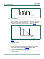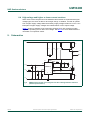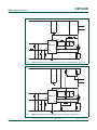
1
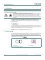
UM10400 UBA3070 demo board Rev. 2 — 10 October 2011 User manual Document information Info Content Keywords UBA3070, switch mode, current source, LED driver, PWM, dimming, analog dimming Abstract The NXP Semiconductors UBA3070 demo board implements a switch-mode current driver for LED strings. By default the board produces 350 mA output current while the maximum output voltage is around 170 V. Multiple user-configurable options are available for the UBA3070 demo board. This user manual describes the UBA3070 demo board version 1.20. Refer to the UBA3070 data sheet for details on the UBA3070 device and application note AN10894 for general application information. UM10400 NXP Semiconductors UBA3070 demo board Revision history Rev Date Description v.2 20111010 second issue v.1 20101204 first issue Contact information For more information, please visit: http://www.nxp.com For sales office addresses, please send an email to: [email protected] UM10400 User manual All information provided in this document is subject to legal disclaimers. Rev. 2 — 10 October 2011 © NXP B.V. 2011. All rights reserved. 2 of 22 UM10400 NXP Semiconductors UBA3070 demo board 1. Introduction WARNING Lethal voltage and fire ignition hazard The non-insulated high voltages that are present when operating this product, constitute a risk of electric shock, personal injury, death and/or ignition of fire. This product is intended for evaluation purposes only. It shall be operated in a designated test area by personnel qualified according to local requirements and labor laws to work with non-insulated mains voltages and high-voltage circuits. This product shall never be operated unattended. The NXP Semiconductors UBA3070 demo board is intended to demonstrate the switch-mode current driving capabilities of the UBA3070 device. Emphasis is on driving LED strings of variable length and color. The LED intensity can be controlled in the following two ways: • PWM dimming • Analog dimming The circuit implements a Boundary Conduction Mode (BCM), buck converter which is a classical text book example of a true switch-mode current source. Boundary Conduction Mode is sometimes also referred to as Critical Conduction Mode. Remark: Unless otherwise stated all voltages are in V (DC). 2. Safety warning This demo board is connected to a high DC voltage or to rectified AC Mains voltage. Avoid touching the reference board during operation. An isolated housing is mandatory when used in uncontrolled, non-laboratory environments. Galvanic isolation of the mains phase using a fixed or variable transformer (Variac) is always recommended. These devices are recognized by the symbols shown in Figure 1. 019aab174 019aab173 a. Isolated Fig 1. UM10400 User manual b. Not isolated Variac isolation symbols All information provided in this document is subject to legal disclaimers. Rev. 2 — 10 October 2011 © NXP B.V. 2011. All rights reserved. 3 of 22 UM10400 NXP Semiconductors UBA3070 demo board 3. Features • Boundary conduction buck converter operates as a true switch-mode current source • Operates with input voltages from 12 V to 190 V and from 12 V to 600 V with some component changes • • • • User configurable output current No custom-made magnetic components required Intrinsically protected against short circuit and open load operation Built-in over-temperature protection. 4. Technical specifications UBA3070 demo board default configuration implements a 350 mA switch-mode current source capable of driving LED strings. These strings can have a total voltage drop of up to 170 V which is equivalent to 60 red or 45 green/blue/white LEDs in series. The maximum supply voltage is 190 V. The board can be reconfigured to meet specific application needs. Some examples of application-specific implementation requirements can be met by changing the components listed in: • Section 8 “Alternative circuit options” on page 12 • Section 9 “Schematics” on page 13 • Section 10 “Component lists” on page 16 See reference Ref. 1 and Ref. 2 for additional information. Table 1. UM10400 User manual Default configuration main characteristics Property Value Remark output current 350 mA selectable; see Ref. 2 supply voltage 12 V to 190 V depends on maximum LED string length AUX supply voltage 12 V 2 mA to 5 mA typical switching frequency 30 kHz to 145 kHz selectable; see Ref. 2 All information provided in this document is subject to legal disclaimers. Rev. 2 — 10 October 2011 © NXP B.V. 2011. All rights reserved. 4 of 22 UM10400 NXP Semiconductors UBA3070 demo board 5. Performance data 5.1 Efficiency The UBA3070 device and the UBA3070 demo board are more suitable for driving longer LED strings. Although there is no fundamental objection to driving short LED strings, high efficiency figures are only obtainable with long LED strings. Figure 2 gives an indication of the typical efficiency that can be expected from a UBA3070 application. In a modified UBA3070 application driving a string of 80 LEDs, 99 % efficiency can be achieved. aaa-000952 100 η (%) 80 60 40 20 0 0 40 80 120 160 Vo (V) Io = 330 mA. Fig 2. Typical efficiency curve for the UBA3070 demo board 5.2 Output current stability The output current varies only slightly with variation of the voltage drop across the LEDs and with variation of the circuit supply voltage. In most circumstances, the light output intensity variation is hardly visible to the human eye (if at all). If necessary, a compensation circuit can be added to the demo board to correct for this output intensity variation. See Section 8 for more detailed information. Figure 3 and Figure 4 show the standard output current stability of the UBA3070 demo board. UM10400 User manual All information provided in this document is subject to legal disclaimers. Rev. 2 — 10 October 2011 © NXP B.V. 2011. All rights reserved. 5 of 22 UM10400 NXP Semiconductors UBA3070 demo board aaa-000953 350 lo (V) 300 250 200 150 100 50 0 60 80 100 120 140 Vo (V) Io = 320 mA typical. Fig 3. Typical output current stability for the UBA3070 demo board under varying supply voltage conditions aaa-000954 350 Io (mA) 300 250 200 150 100 50 0 140 150 160 170 180 190 200 210 Vsupply (V) Io = 320 mA typical. Fig 4. Typical output current stability for the UBA3070 demo board under varying load condition The L1 inductor value (see circuit diagram in Figure 9) has an influence on the operation of the UBA3070 circuit. As can be concluded from application note AN10894, the main parameter affected is the switching frequency. Variations up to 10 % of the L1 inductance value, however, have practically no influence on the LED output current value. The UBA3070 application is minimally affected by production-related spread of the L1 inductor. Figure 5 gives an impression of this immunity. UM10400 User manual All information provided in this document is subject to legal disclaimers. Rev. 2 — 10 October 2011 © NXP B.V. 2011. All rights reserved. 6 of 22 UM10400 NXP Semiconductors UBA3070 demo board aaa-000955 350 lo (mA) 300 250 200 150 100 50 0 450 500 550 600 650 L1 (μH) Io = 320 mA typical. Fig 5. UM10400 User manual Typical output current variation of the UBA3070 demo board as a result of varying L1 value All information provided in this document is subject to legal disclaimers. Rev. 2 — 10 October 2011 © NXP B.V. 2011. All rights reserved. 7 of 22 UM10400 NXP Semiconductors UBA3070 demo board 6. Connection of the demo board The UBA3070 demo board connections are shown in Figure 6. When no connection is made to the dimming pin, the LEDs are at full intensity. The AUX voltage is between 12 V and 15 V. The supply voltage can be between 12 V and 190 V. The supply voltage must be at least 10 % above the LED string voltage (at rated current). It is recommended headroom of at least 20 % is allowed. GND (0 V) Dimming AUX voltage Supply voltage Fig 6. UM10400 User manual LED string anode LED string cathode aaa-000956 UBA3070 demo board connections All information provided in this document is subject to legal disclaimers. Rev. 2 — 10 October 2011 © NXP B.V. 2011. All rights reserved. 8 of 22 UM10400 NXP Semiconductors UBA3070 demo board 7. Circuit description The circuit on the UBA3070 demo board consists of several sections: power supply input, dimming input, switching, current measurement/feedback and output. The UBA3070 full default circuit diagram implemented on the demo board is shown in Figure 9. The component is shown in Table 3. 7.1 Power supply input section The power supply input section consists of two energy reservoirs and filters: • The main supply voltage reservoir and noise filter - capacitors C1 and C10 • The auxiliary supply voltage reservoir and noise filter - capacitors C2 and C8 The main supply power (12 V to 190 V) is connected to connectors J1.4 (positive) and J1.1 (negative/GND). The main power is predominantly used for providing power to the LED string. The auxiliary supply voltage (12 V to 15 V) is connected to connectors J1.3 (positive) and J1.1 (negative/GND). The auxiliary supply powers the internal circuitry of the UBA3070 IC. This supply also provides the power for charging and discharging MOSFET Q1 gate. The amount of energy required to charge and discharge Ciss of MOSFET Q1 is the dominant factor which determines the auxiliary supply current consumption. The current requirement can be as low as 2 mA for a small MOSFET. However, for a large MOSFET, it could be one order of magnitude higher. 7.2 Dimming input section The dimming input signal is supplied to connectors J1.2 (positive/signal) and J1.1 (GND). Using a low-pass and current limiting network (R1, R2, C3), the dimming input signal is supplied to the PWM pin. The dimming signal can be both a digital PWM signal and an analog signal. 7.2.1 PWM dimming When a high voltage (Vhigh, >2.5 V) is fed to the PWM pin, the converter is effectively disabled (in cycle skipping mode). A low voltage (Vlow, <0.5 V) on the same pin causes the UBA3070 to be fully enabled. The light output produced can be varied by toggling between low voltage and high voltage. The light output is exactly proportional to the duty ratio of the PWM dimming signal. In principle, any PWM frequency is acceptable for PWM dimming. However, in reality, a low PWM frequency can give the impression that the LED string is flickering. A high frequency can result in inaccurate dimming performance and interference with the UBA3070 circuit operating frequency (see Ref. 2). A PWM frequency in the range of 100 Hz to 1 kHz is recommended for most applications including general lighting and LCD TV backlighting. The relative light output intensity is given in Equation 1 t low intensity = ------------------------------- 100 % t high + t low UM10400 User manual All information provided in this document is subject to legal disclaimers. Rev. 2 — 10 October 2011 (1) © NXP B.V. 2011. All rights reserved. 9 of 22 UM10400 NXP Semiconductors UBA3070 demo board V tlow thigh Vhigh Vlow t aaa-000957 Fig 7. Typical PWM dimming signal 7.2.2 Analog dimming By feeding an analog voltage signal to the PWM pin, the magnitude of the peak current flowing through the L1 inductor can be controlled. The analog control voltage on the control pin is between 1 V and 2 V approximately. In that voltage range, the magnitude of the voltage is roughly inversely proportional to the VSENSE voltage of the UBA3070 IC. Consequently, the light intensity control matches the curve shown in Figure 8. VSENSE(max) 0.52 V 1V (typ) 1.5 V (typ) VPWM aaa-000958 Fig 8. Typical analog control light intensity is proportional to the VSENSE level A simple circuit that could be used to experiment with analog dimming is shown in Figure 13. 7.3 Switching section The heart of the switching section is the UBA3070 IC (IC1). Together with the power components Q1, D3, L1 and R6, IC1 forms the switching section. When the UBA3070 switches MOSFET Q1 on, the current in L1 ramps up. When UBA3070 switches off Q1, the L1 current continues to flow through D3 and ramps down. R6 is a current sense resistor that is in the high current path. See Section 7.4 for further details. 7.4 Current measurement and feedback section The operation of the UBA3070 Boundary mode buck converter relies on the measurement of two current levels: UM10400 User manual All information provided in this document is subject to legal disclaimers. Rev. 2 — 10 October 2011 © NXP B.V. 2011. All rights reserved. 10 of 22 UM10400 NXP Semiconductors UBA3070 demo board • The detection of the peak inductor current level while MOSFET Q1 is on (primary stroke) • The detection of zero inductor current while MOSFET Q1 is off and the current is flowing through D3 (secondary stroke) The average current that is supplied by the switching section is exactly half the inductor peak current. This is because of the current ramping up and down with a constant slope and there is no dead-time between two subsequent cycles. 7.4.1 Peak current detection The peak inductor current is detected by measuring the voltage drop across R6. This voltage drop is presented to the UBA3070 sense pin, and the UBA3070 reacts to the detection of the peak current by switching off MOSFET Q1. 7.4.2 Direct demagnetization detection Zero inductor current is detected by measuring the inductor current with resistor R4. The information is transferred using the asymmetric current mirror Q2, Q3, R4 and R7 to the network R3, R5, C4, D1 and D2. When the voltage supplied to the UBA3070 MASK pin drops below 100 mV, the UBA3070 IC reacts by switching on MOSFET Q1. This way of detecting zero current (or demagnetization) of the inductor is called “direct demagnetization detection”. An alternative way of demagnetization detection is explained in Section 8. 7.5 Output section The switching section produces a sawtooth current waveform in the inductor. Current ramps-up linearly from 0 A to Ipeak and then ramps down linearly from Ipeak to 0 A. In most circumstances, this current waveform is not fed directly to an LED string. Capacitor C6 is used in the output section to reduce the ripple on the LED current for that reason. See Ref. 2 for details about the dimensioning of the ripple filter. The LED string is connected to connectors J2.1 (cathode of the LED string) and J2.2 (anode of the LED string). UM10400 User manual All information provided in this document is subject to legal disclaimers. Rev. 2 — 10 October 2011 © NXP B.V. 2011. All rights reserved. 11 of 22 UM10400 NXP Semiconductors UBA3070 demo board 8. Alternative circuit options 8.1 Indirect demagnetization detection The UBA3070 demo board offers the possibility to implement a cheaper and simpler alternative demagnetization detection circuit than the standard direct demagnetization detection option. The disadvantages of indirect demagnetization detection are: • its performance is lower with less accurate current regulation and • the possibility of false zero current detection for a dynamically changing load. However for general lighting purposes, this demagnetization detection option is adequate. Indirect demagnetization detection relies on the phenomenon that a ringing voltage appears at the drain node of MOSFET Q1 when the secondary stroke has finished. Resonance between inductor L1 and the (parasitic) capacitance CDS of Q1 cause the ringing voltage. The resonating waveform propagates through capacitor C9 and resistor R10 to the R3, R5, C4, D1, D2 network and to the UBA3070 MASK pin. The first valley of the ringing signal causes the MASK pin voltage to drop below 100 mV. In that sense, this method is an indirect way of detecting demagnetization of the L1 inductor. The UBA3070 circuit using indirect demagnetization detection is shown in Figure 10. The component changes are listed in Table 4. 8.2 Rising slope compensation The UBA3070 data sheet (Ref. 1) shows that there is always a time delay between peak current detection through the SENSE pin and the MOSFET switching off. This propagation delay is typically 140 ns and causes overshooting of the peak inductor current. The steeper the slope of the rising current, the higher the overshoot. The slope-dependent overshoot is “neutralized” using a simple high-pass filter in the peak current detection circuit. Instead of using R6 for peak current detection, a frequency-dependent divider (R8, R9, C5) is added before the signal is fed back to the SENSE pin. Depending on the UBA3070 driver circuit implementation, some recalculation and/or experimentation is required to find proper values for R8, R9 and C5. The UBA3070 circuit diagram with rising slope compensation is shown in Figure 11. The component changes are listed in Table 5. 8.3 Minimal application with relaxed noise immunity and protections To save costs, some of the noise immunity and (current limiting) protection functions of the UBA3070 application can be sacrificed. In that way, a simple circuit with few components is obtained. It is left to the judgment of the design engineer whether, in specific circumstances, these simplifications are acceptable. Figure 12 shows a minimal UBA3070 circuit diagram that is still fully functional. Take care how and under what circumstances it is operated. The component changes are listed in Table 6. UM10400 User manual All information provided in this document is subject to legal disclaimers. Rev. 2 — 10 October 2011 © NXP B.V. 2011. All rights reserved. 12 of 22 UM10400 NXP Semiconductors UBA3070 demo board 8.4 High voltage and higher or lower current versions When some of the components of the UBA3070 demo board are replaced with higher voltage types, the driver is able to drive longer strings. In addition, it is able to operate from a higher supply voltage while the auxiliary supply voltage remains at 12 V to 15 V. Examples of higher supply voltages are rectified mains or PFC output voltage. Table 7 shows an example of the component changes for a 100 mA driver module capable of operating from a 400 V PFC voltage. See Ref. 2 for more details about the calculation of component values. 9. Schematics J1.4 R7 C1 C10 D3 R4 R4a Q2 Q3 J2.2 C6 J2.1 L1 DRAIN IC1 8 VCC J1.3 4 MASK R3 C4 1 R5 D1 D2 Q1 C2 UBA3070 C8 R1 PWM J1.2 7 2 C3 R2 HVS 3 5 SENSE R8 GND R6 R6a J1.1 aaa-000959 Fig 9. UM10400 User manual UBA3070 demo board circuit diagram with direct demagnetization detection (default implementation) All information provided in this document is subject to legal disclaimers. Rev. 2 — 10 October 2011 © NXP B.V. 2011. All rights reserved. 13 of 22 UM10400 NXP Semiconductors UBA3070 demo board J1.4 J3 C1 J2.2 C10 D3 C6 J2.1 L1 C9 R10 DRAIN IC1 8 VCC J1.3 4 MASK R3 C4 1 R5 D1 D2 Q1 C2 UBA3070 C8 R1 PWM J1.2 7 5 2 C3 HVS 3 R2 R8 SENSE GND R6 R6a J1.1 aaa-000960 Fig 10. UBA3070 demo board circuit diagram with indirect demagnetization detection J1.4 R7 C1 C10 D3 R4 R4a Q2 Q3 J2.2 C6 J2.1 L1 DRAIN IC1 8 VCC J1.3 4 MASK R3 C4 1 R5 D1 D2 Q1 C2 UBA3070 C8 R1 PWM J1.2 7 3 2 C3 R2 HVS 5 R8 SENSE C5 GND R6 R6a R9 J1.1 aaa-000961 Fig 11. UBA3070 demo board circuit diagram with rising slope compensation UM10400 User manual All information provided in this document is subject to legal disclaimers. Rev. 2 — 10 October 2011 © NXP B.V. 2011. All rights reserved. 14 of 22 UM10400 NXP Semiconductors UBA3070 demo board J1.4 J2.2 D3 C1 C6 J2.1 L1 DRAIN IC1 8 VCC J1.3 R3 MASK 4 R10 C9 R5 1 Q1 UBA3070 PWM J1.2 HVS 7 3 SENSE 5 2 GND R6 J1.1 aaa-000962 Fig 12. UBA3070 demo board circuit diagram for minimal application J1.4 R7 C1 C10 D3 R4 R4a Q2 Q3 J2.2 C6 J2.1 L1 J101.3 DRAIN IC1 R101 8 VCC J1.3 4 MASK R3 C4 1 R5 D1 D2 R102 Q1 C2 J101.2 D101 C8 R1 R103 C101 UBA3070 PWM J1.2 7 3 2 C3 R104 R2 HVS 5 SENSE R8 GND R6 J101.1 R6a J1.1 aaa-000963 Fig 13. UBA3070 demo board circuit diagram with simple analog dimming extension UM10400 User manual All information provided in this document is subject to legal disclaimers. Rev. 2 — 10 October 2011 © NXP B.V. 2011. All rights reserved. 15 of 22 UM10400 NXP Semiconductors UBA3070 demo board Connect terminal J101.3 to J1.3, J101.2 to J1.2 and J101.1 to J1.1 to use the simple analog dimming circuit: with all voltages applied to the UBA3070 module as described in Table 6 and Section 7.1. See Table 2 for suggested component values. Table 2. Suggested component list for the simple analog dimming extension circuit Ref. Description and package Manufacturer Remarks D101 BZX384C5V1; SOD323 NXP Semiconductors - C101 220 nF, 10 V - - R101 12 k - - R102 4.7 k - [1] R103 2 k - potentiometer R104 1.5 k - [1] [1] To use the full range of the R103 potentiometer, the values of R102 and R104 may need adapting. 10. Component lists Table 3. UM10400 User manual Default component list Ref. Description and package Manufacturer Remarks IC1 UBA3070; SO8 NXP Semiconductors - Q1 PHD9NQ20T; DPAK NXP Semiconductors - Q1a varies; SOT223 varies not mounted Q2 BCP51; SOT223 NXP Semiconductors - Q3 BF723; SOT223 NXP Semiconductors - D1 BAS316; SOD323 NXP Semiconductors - D2 BAS316; SOD323 NXP Semiconductors - D3 BYG20J; DO-214AC Vishay - L1 560 H, 680 mA, ELC10D561E; 2E pitch - 10 mm maximum C1 22 F, 200 V; 2E pitch - 13 mm maximum C2 100 F, 25 V; 1E pitch - 8 mm maximum C3 180 pF, 50 V; 1206 - - C4 22 pF, 50 V; 1206 - - C5 varies; 1206 - not mounted C6 100 nF, 250 V; 2E pitch - maximum size 13 5 mm C7 varies; 1206 - not mounted C8 100 nF, 50 V; 1206 - - C9 330 pF, 250 V; 1206 - not mounted C10 10 nF, 500 V; 1206 - - R1 1 k; 1206 - - R2 10 k; 1206 - - R3 22 k; 1206 - - R4 1.5 , 0,25 W; 1206 - - R4a 1.5 , 0.25 W; 1206 - - All information provided in this document is subject to legal disclaimers. Rev. 2 — 10 October 2011 © NXP B.V. 2011. All rights reserved. 16 of 22 UM10400 NXP Semiconductors UBA3070 demo board Table 3. Ref. Description and package Manufacturer Remarks R5 10 k; 1206 - - R6 1.5 , 0.25 W; 1206 - - R6a 1.5 , 0.25 W; 1206 - - R7 510 ; 1206 - - R8 0 (jumper); 1206 - - R9 varies; 1206 - not mounted R10 22 k; 1206 - not mounted J1 4-pole terminal block; 2E pitch - for example, Phoenix:1729144 J2 2-pole terminal block; 2E pitch - for example, Phoenix: 1729128 J3 jumper wire - not mounted Table 4. Ref. Description and package Manufacturer/Supplier Remarks BCP51; SOT223 NXP Semiconductors not mounted Q3 BF723; SOT223 NXP Semiconductors not mounted C9 330 pF, 250 V; 1206 R4 1.5 , 0,25 W; 1206 not mounted R4a 1.5 , 0.25 W; 1206 not mounted R5 1 k; 1206 R7 510 ; 1206 R10 22 k; 1206 J3 Jumper wire not mounted install Component list modification rising slope compensation Ref. Description and package Manufacturer Remarks C5 varies; 1206 - [1] R8 varies; 1206 - [1] R9 varies; 1206 - [1] [1] User manual Component list modification for indirect demagnetization detection Q2 Table 5. UM10400 Default component list See application note AN10894 (Ref. 2) for guidelines. All information provided in this document is subject to legal disclaimers. Rev. 2 — 10 October 2011 © NXP B.V. 2011. All rights reserved. 17 of 22 UM10400 NXP Semiconductors UBA3070 demo board Table 6. Ref. Description and package Manufacturer Remarks Q2 BCP51; SOT223 NXP Semiconductors not mounted Q3 BF723; SOT223 NXP Semiconductors not mounted D1 BAS316; SOD323 NXP Semiconductors not mounted D2 BAS316; SOD323 NXP Semiconductors not mounted C2 100 F, 25 V; 1E pitch - not mounted C3 180 pF, 50 V; 1206 - not mounted C4 22 pF, 50 V; 1206 - not mounted C8 100 nF, 50 V; 1206 - not mounted C9 330 pF, 250 V; 1206 - - C10 10 nF, 500 V; 1206 - not mounted R1 0 (short / jumper); 1206 - - R2 10 k; 1206 - not mounted R4 1.5 , 0,25 W; 1206 - not mounted R4a 1.5 , 0.25 W; 1206 - not mounted R5 1 k; 1206 - - R6 0.75 , 0.25 W; 1206 - - R6a 1.5 ; 0.25 W; 1206 - not mounted R7 510 ; 1206 - not mounted R10 22 k; 1206 - - J3 jumper wire - install Table 7. UM10400 User manual Component list modification for minimal application Component list modification for 400 V, 100 mA driver Ref. Description and package Manufacturer/ Supplier Remarks Q1 PHD9NQ20T; DPAK - not mounted Q1a BSP299; SOT223 Infineon - Q3 PBHV9040Z; SOT223 NXP Semiconductors - L1 4.7 mH, 200 mA, ELC11D472F; 2E pitch - 12 mm maximum C1 10 F, 400 V; 2E pitch - 13 mm maximum C6 33 F, 400 V; 2E to 4E pitch - maximum size 13 5 mm R4 2.2 , 0,25 W; 1206 - - R4a 1.5 ; 0.25 W; 1206 - not mounted R6 2.2 , 0.25 W; 1206 - - R6a 1.5 ; 0.25 W; 1206 - not mounted All information provided in this document is subject to legal disclaimers. Rev. 2 — 10 October 2011 © NXP B.V. 2011. All rights reserved. 18 of 22 UM10400 NXP Semiconductors UBA3070 demo board 11. Printed-Circuit Board (PCB) The UBA3070 demo board PCB is a single-sided board. Dimensions are approximately 38 41 mm. The demo boards are produced on 1.6 mm FR4 with single-sided 35 m copper (1 oz.). FR2 can also be used as the PCB material. The PCB can accommodate several implementations of the NXP Semiconductors UBA3070 demo board as outlined in Section 7, Section 8, Section 9 and Section 10. The Gerber File set for the production of the PCBs is available from NXP Semiconductors. The bottom silk is normally not used for PCB production. It is only a component position reference. aaa-000964 a. Bottom solder mask aaa-000965 b. Bottom Cu layer aaa-000967 aaa-000966 c. Top silk d. Bottom silk Fig 14. PCB layouts UM10400 User manual All information provided in this document is subject to legal disclaimers. Rev. 2 — 10 October 2011 © NXP B.V. 2011. All rights reserved. 19 of 22 UM10400 NXP Semiconductors UBA3070 demo board 12. References UM10400 User manual [1] Data sheet — UBA3070 LED backlight driver IC. [2] Application note — AN10894 Application aspects of the UBA3070 switch mode LED driver. All information provided in this document is subject to legal disclaimers. Rev. 2 — 10 October 2011 © NXP B.V. 2011. All rights reserved. 20 of 22 UM10400 NXP Semiconductors UBA3070 demo board 13. Legal information 13.1 Definitions Draft — The document is a draft version only. The content is still under internal review and subject to formal approval, which may result in modifications or additions. NXP Semiconductors does not give any representations or warranties as to the accuracy or completeness of information included herein and shall have no liability for the consequences of use of such information. Export control — This document as well as the item(s) described herein may be subject to export control regulations. Export might require a prior authorization from competent authorities. 13.2 Disclaimers Limited warranty and liability — Information in this document is believed to be accurate and reliable. However, NXP Semiconductors does not give any representations or warranties, expressed or implied, as to the accuracy or completeness of such information and shall have no liability for the consequences of use of such information. In no event shall NXP Semiconductors be liable for any indirect, incidental, punitive, special or consequential damages (including - without limitation - lost profits, lost savings, business interruption, costs related to the removal or replacement of any products or rework charges) whether or not such damages are based on tort (including negligence), warranty, breach of contract or any other legal theory. Notwithstanding any damages that customer might incur for any reason whatsoever, NXP Semiconductors’ aggregate and cumulative liability towards customer for the products described herein shall be limited in accordance with the Terms and conditions of commercial sale of NXP Semiconductors. Right to make changes — NXP Semiconductors reserves the right to make changes to information published in this document, including without limitation specifications and product descriptions, at any time and without notice. This document supersedes and replaces all information supplied prior to the publication hereof. Suitability for use — NXP Semiconductors products are not designed, authorized or warranted to be suitable for use in life support, life-critical or safety-critical systems or equipment, nor in applications where failure or malfunction of an NXP Semiconductors product can reasonably be expected to result in personal injury, death or severe property or environmental damage. NXP Semiconductors accepts no liability for inclusion and/or use of NXP Semiconductors products in such equipment or applications and therefore such inclusion and/or use is at the customer’s own risk. Applications — Applications that are described herein for any of these products are for illustrative purposes only. NXP Semiconductors makes no representation or warranty that such applications will be suitable for the specified use without further testing or modification. Customers are responsible for the design and operation of their applications and products using NXP Semiconductors products, and NXP Semiconductors accepts no liability for any assistance with applications or customer product design. It is customer’s sole responsibility to determine whether the NXP Semiconductors product is suitable and fit for the customer’s applications and products planned, as well as for the planned application and use of customer’s third party customer(s). Customers should provide appropriate design and operating safeguards to minimize the risks associated with their applications and products. UM10400 User manual NXP Semiconductors does not accept any liability related to any default, damage, costs or problem which is based on any weakness or default in the customer’s applications or products, or the application or use by customer’s third party customer(s). Customer is responsible for doing all necessary testing for the customer’s applications and products using NXP Semiconductors products in order to avoid a default of the applications and the products or of the application or use by customer’s third party customer(s). NXP does not accept any liability in this respect. Evaluation products — This product is provided on an “as is” and “with all faults” basis for evaluation purposes only. NXP Semiconductors, its affiliates and their suppliers expressly disclaim all warranties, whether express, implied or statutory, including but not limited to the implied warranties of non-infringement, merchantability and fitness for a particular purpose. The entire risk as to the quality, or arising out of the use or performance, of this product remains with customer. In no event shall NXP Semiconductors, its affiliates or their suppliers be liable to customer for any special, indirect, consequential, punitive or incidental damages (including without limitation damages for loss of business, business interruption, loss of use, loss of data or information, and the like) arising out the use of or inability to use the product, whether or not based on tort (including negligence), strict liability, breach of contract, breach of warranty or any other theory, even if advised of the possibility of such damages. Notwithstanding any damages that customer might incur for any reason whatsoever (including without limitation, all damages referenced above and all direct or general damages), the entire liability of NXP Semiconductors, its affiliates and their suppliers and customer’s exclusive remedy for all of the foregoing shall be limited to actual damages incurred by customer based on reasonable reliance up to the greater of the amount actually paid by customer for the product or five dollars (US$5.00). The foregoing limitations, exclusions and disclaimers shall apply to the maximum extent permitted by applicable law, even if any remedy fails of its essential purpose. Safety of high-voltage evaluation products — The non-insulated high voltages that are present when operating this product, constitute a risk of electric shock, personal injury, death and/or ignition of fire. This product is intended for evaluation purposes only. It shall be operated in a designated test area by personnel that is qualified according to local requirements and labor laws to work with non-insulated mains voltages and high-voltage circuits. The product does not comply with IEC 60950 based national or regional safety standards. NXP Semiconductors does not accept any liability for damages incurred due to inappropriate use of this product or related to non-insulated high voltages. Any use of this product is at customer’s own risk and liability. The customer shall fully indemnify and hold harmless NXP Semiconductors from any liability, damages and claims resulting from the use of the product. 13.3 Trademarks Notice: All referenced brands, product names, service names and trademarks are the property of their respective owners. All information provided in this document is subject to legal disclaimers. Rev. 2 — 10 October 2011 © NXP B.V. 2011. All rights reserved. 21 of 22 UM10400 NXP Semiconductors UBA3070 demo board 14. Contents 1 2 3 4 5 5.1 5.2 6 7 7.1 7.2 7.2.1 7.2.2 7.3 7.4 7.4.1 7.4.2 7.5 8 8.1 8.2 8.3 8.4 9 10 11 12 13 13.1 13.2 13.3 14 Introduction . . . . . . . . . . . . . . . . . . . . . . . . . . . . 3 Safety warning . . . . . . . . . . . . . . . . . . . . . . . . . . 3 Features . . . . . . . . . . . . . . . . . . . . . . . . . . . . . . . 4 Technical specifications . . . . . . . . . . . . . . . . . . 4 Performance data. . . . . . . . . . . . . . . . . . . . . . . . 5 Efficiency . . . . . . . . . . . . . . . . . . . . . . . . . . . . . 5 Output current stability . . . . . . . . . . . . . . . . . . . 5 Connection of the demo board. . . . . . . . . . . . . 8 Circuit description . . . . . . . . . . . . . . . . . . . . . . . 9 Power supply input section . . . . . . . . . . . . . . . . 9 Dimming input section . . . . . . . . . . . . . . . . . . . 9 PWM dimming . . . . . . . . . . . . . . . . . . . . . . . . . 9 Analog dimming . . . . . . . . . . . . . . . . . . . . . . . 10 Switching section . . . . . . . . . . . . . . . . . . . . . . 10 Current measurement and feedback section . 10 Peak current detection . . . . . . . . . . . . . . . . . . 11 Direct demagnetization detection . . . . . . . . . . 11 Output section . . . . . . . . . . . . . . . . . . . . . . . . 11 Alternative circuit options. . . . . . . . . . . . . . . . 12 Indirect demagnetization detection . . . . . . . . . 12 Rising slope compensation. . . . . . . . . . . . . . . 12 Minimal application with relaxed noise immunity and protections . . . . . . . . . . . . . . . . . . . . . . . . 12 High voltage and higher or lower current versions . . . . . . . . . . . . . . . . . . . . . . . . . . . . . 13 Schematics . . . . . . . . . . . . . . . . . . . . . . . . . . . . 13 Component lists. . . . . . . . . . . . . . . . . . . . . . . . 16 Printed-Circuit Board (PCB) . . . . . . . . . . . . . . 19 References . . . . . . . . . . . . . . . . . . . . . . . . . . . . 20 Legal information. . . . . . . . . . . . . . . . . . . . . . . 21 Definitions . . . . . . . . . . . . . . . . . . . . . . . . . . . . 21 Disclaimers . . . . . . . . . . . . . . . . . . . . . . . . . . . 21 Trademarks. . . . . . . . . . . . . . . . . . . . . . . . . . . 21 Contents . . . . . . . . . . . . . . . . . . . . . . . . . . . . . . 22 Please be aware that important notices concerning this document and the product(s) described herein, have been included in section ‘Legal information’. © NXP B.V. 2011. All rights reserved. For more information, please visit: http://www.nxp.com For sales office addresses, please send an email to: [email protected] Date of release: 10 October 2011 Document identifier: UM10400