1
B O A R D
H A R D W A R E
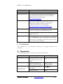
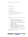
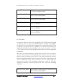
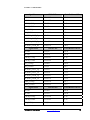
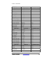
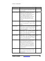
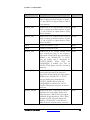
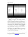
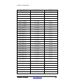
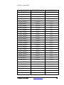
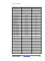
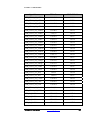
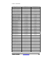
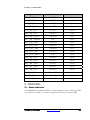
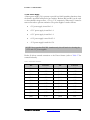
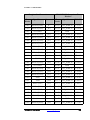
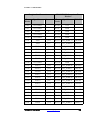
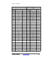
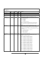
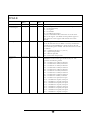
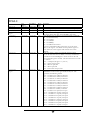
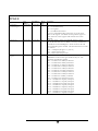
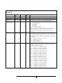
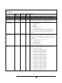
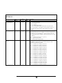
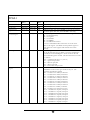
SYS_ICLKp
U79.J22
U65.29
SYS_ICLKn
U79.K22
U65.30
RCKTIO_OSCT_Ip
U79.G22
U68.14
RCKTIO_OSCT_In
U79.F22
U68.15
RCKTIO_OSCB_Ip
U79.AU22
U68.11
RCKTIO_OSCB_In
U79.AT22
U68.12
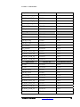
DDR_ICLKp
U79.AT21
U66. 5
DDR_ICLKn
U79.AU21
U66.6
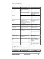
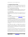
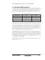
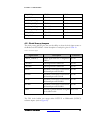
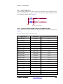
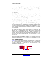
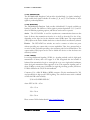
4.2 Clock Source Jumpers
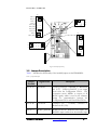
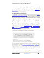
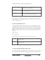
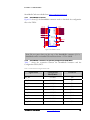
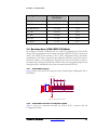
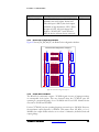
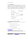
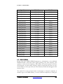
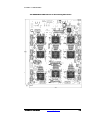
The clock source grid JP5 gives the user the ability to select the clock input source to
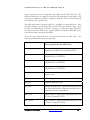
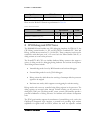
the RoboClock PLL buffers. A brief description of each pin is given in Table 10.
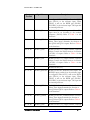
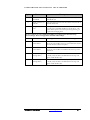
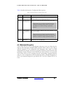
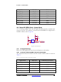
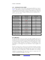
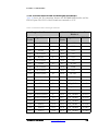
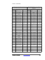
Table 10 - Clock Source Signals
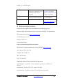
Signal Name
Description
Connector
CFPGA_CLKOUT
Clock signal from the Configuration JP5.A3
FPGA.
CLOCKA
Clock signal from oscillator X3
JP5.A1
CLOCKB
Clock signal from oscillator X2
JP5.A5
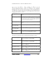
PLL1B
Secondary clock input to RoboClock, JP5.B4
differential pair with PLL1BN
PLL1BN
Secondary clock input to RoboClock, JP5.B5
differential pair with1 PLL1B
PLL2B
Secondary clock input to RoboClock, JP5.B1
differential pair with PLL2BN
PLL2BN
Secondary clock input to RoboClock, JP5.B2
differential pair with PLL2BN
GND
Provides a ground reference for signals JP5.C1..C5
in the ribbon cable.
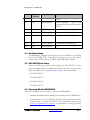
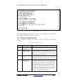
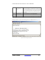
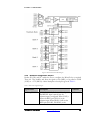
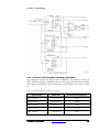
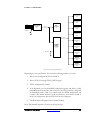
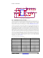
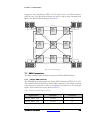
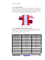
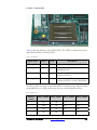
The PLL clock buffers can accept either LVTTL33 or Differential (LVPECL)
reference inputs (refer to Figure 22).
DN6000K10 User Guide
www.dinigroup.com
77