1
Configuration Programming of UCD Devices
This document describes techniques that can be used to download a device
configuration to a Texas Instruments UCD device. While this document references
version 1.8.95 of the Fusion Digital Power Designer software, you can use versions
newer than 1.8.95 as well.
Last Updated 28 September 2011
Michael S Muegel
Bill Waters (JTAG)
Configuration Programming of UCD Devices
IMPORTANT NOTICE
Texas Instruments and its subsidiaries (TI) reserve the right to make changes to their products or to discontinue any
product or service without notice, and advise customers to obtain the latest version of relevant information to verify,
before placing orders, that information being relied on is current and complete. All products are sold subject to the
terms and conditions of sale supplied at the time of order acknowledgment, including those pertaining to warranty,
patent infringement, and limitation of liability.
TI warrants performance of its products to the specifications applicable at the time of sale in accordance with TI’s
standard warranty. Testing and other quality control techniques are utilized to the extent TI deems necessary to
support this warranty. Specific testing of all parameters of each device is not necessarily performed, except those
mandated by government requirements.
Customers are responsible for their applications using TI components.
In order to minimize risks associated with the customer’s applications, adequate design and operating safeguards
must be provided by the customer to minimize inherent or procedural hazards.
TI assumes no liability for applications assistance or customer product design. TI does not warrant or represent that
any license, either express or implied, is granted under any patent right, copyright, mask work right, or other
intellectual property right of TI covering or relating to any combination, machine, or process in which such products or
services might be or are used. TI’s publication of information regarding any third party’s products or services does not
constitute TI’s approval, license, warranty or endorsement thereof.
Reproduction of information in TI data books or data sheets is permissible only if reproduction is without alteration
and is accompanied by all associated warranties, conditions, limitations and notices. Representation or reproduction
of this information with alteration voids all warranties provided for an associated TI product or service, is an unfair
and deceptive business practice, and TI is not responsible nor liable for any such use.
Resale of TI’s products or services with statements different from or beyond the parameters stated by TI for that
product or service voids all express and any implied warranties for the associated TI product or service, is an unfair
and deceptive business practice, and TI is not responsible nor liable for any such use.
Also see: Standard Terms and Conditions of Sale for Semiconductor Products. www.ti.com/sc/docs/stdterms.htm
Mailing Address:
Texas Instruments
Post Office Box 655303
Dallas, Texas 75265
Copyright © 2009, Texas Instruments Incorporated
Texas Instruments
Page i
Configuration Programming of UCD Devices
Table of Contents
1
Introduction ................................................................................................................................................................ 4
2
Configuration Basics ................................................................................................................................................ 5
3
An Overview of Configuration Programming Options......................................................................................... 6
4
Configuration Export Overview ............................................................................................................................... 7
4.1
Export Using the Fusion GUI ............................................................................................................................. 7
4.2
Exporting to Multiple File Formats ..................................................................................................................... 9
4.3
Configuring Export Options .............................................................................................................................. 10
4.4
Exporting One File at a Time ........................................................................................................................... 10
4.5
Export Using the FusionDeviceExporter Command Line Tool....................................................................... 10
5
Data Flash Considerations ..................................................................................................................................... 12
6
Programming Options and Instructions .............................................................................................................. 14
6.1
Downloading a Configuration via Fusion Tools............................................................................................... 14
6.1.1
Fusion Digital Power Designer .................................................................................................................... 14
6.1.2
Firmware and Project File Download Tool .................................................................................................. 14
6.1.3
FusionConfigWriter Command Line Tool .................................................................................................... 15
6.1.4
Fusion Manufacturing GUI (MFR GUI) ....................................................................................................... 17
6.2
Downloading a Configuration Using a Dedicated EEPROM Programmer .................................................... 21
6.3
Downloading a Configuration via JTAG .......................................................................................................... 22
6.3.1
System Board Requirements ....................................................................................................................... 22
6.3.2
Overview of SVF .......................................................................................................................................... 22
6.3.3
Differences Between IC Packages .............................................................................................................. 22
6.3.4
Exporting Data Flash Configuration as SVF ............................................................................................... 23
6.3.5
SVF Flow ...................................................................................................................................................... 23
6.3.6
BSDL File ...................................................................................................................................................... 24
6.3.7
Supported TCK Frequencies ....................................................................................................................... 24
6.3.8
List of Tested Programmers ........................................................................................................................ 24
6.3.9
Troubleshooting ............................................................................................................................................ 24
6.3.10 Additional Information & Help ...................................................................................................................... 25
6.4
Downloading Configuration Data Using a Microcontroller .............................................................................. 26
6.4.1
SMBus / I2C Script Overview ....................................................................................................................... 26
6.4.2
Microcontroller Writes Data Flash ............................................................................................................... 28
6.4.2.1
Microcontroller Writes Data Flash, Normal Mode Scheme .............................................................. 28
6.4.2.2
Microcontroller Writes Data Flash, ROM Mode Scheme .................................................................. 29
Texas Instruments
Page ii
Configuration Programming of UCD Devices
6.4.3
Microcontroller Writes Full Configuration via PMBus ................................................................................. 30
6.4.4
Microcontroller Writes Partial Configuration via PMBus ............................................................................ 30
6.4.5
Testing the Export Using the Script Runner Tool ....................................................................................... 30
6.4.5.1
Script Runner GUI Tool ...................................................................................................................... 30
6.4.5.2
FusionScriptRunner Command Line Tool ......................................................................................... 33
7
Tips............................................................................................................................................................................. 34
8
Frequently Asked Questions (FAQs) .................................................................................................................... 35
8.1
Why do I need to be connected to a device to export hex or SVF? .............................................................. 35
8.2
Do I need to be connected to my system board to export data flash or SVF, or will any board do? ........... 35
8.3
Is there a data flash checksum I can read to validate that the flash has been programmed correctly?...... 36
8.4
How does the device validate that its data flash has not been corrupted? ................................................... 36
8.5
How can I verify that my configuration programming process downloaded the correct file and the
configuration was loaded by the device without error? ................................................................................................ 38
8.6
9
Miscellaneous JTAG Questions ....................................................................................................................... 38
Appendices ............................................................................................................................................................... 41
9.1
Exporting Configuration Data Flash Hex File .................................................................................................. 41
9.2
Firmware Versions, Program Flash Checksums, and Programming Modes for Released Devices ........... 44
9.3
Gang Programmer Notes ................................................................................................................................. 46
9.4
Comparison of Write Times .............................................................................................................................. 47
9.5
Detailed Recipe for Device Writes Data Flash, Normal Mode Scheme ........................................................ 48
9.6
Data Flash Download Script Example – Normal Mode .................................................................................. 53
9.7
Data Flash Download Script Example – ROM Mode...................................................................................... 54
9.8
PMBus Config Script Examples ....................................................................................................................... 56
9.8.1
UCD9224 PMBus Config Script Example ................................................................................................... 56
9.8.2
UCD90124 PMBus Config Script Example ................................................................................................. 61
9.9
Packet Error Checking (PEC) Algorithm Sample C Code .............................................................................. 66
Texas Instruments
Page iii
Configuration Programming of UCD Devices
1
INTRODUCTION
This document describes how configuration data can be written (programmed) to select Texas Instruments UCD
devices. Currently this covers UCD92xx digital power controller and UCD90xx sequencers and system health
controllers. Generally, any device that is configured with the Fusion Digital Power Designer software and is a UCD
device should support the programming options described here. For example, the UCD908x power supply sequencer
and monitor is not supported. The UCD908x does not support PMBus and is configured by a different GUI.
Both UCD92xx and UCD90xx device families use the same IC underlying memory, ROM, and PMBus architecture.
This IC architecture, generically referred to as the UCD30xx, comes in four different pin/package configurations: 40,
48, 64, and 80 pins. Most devices only come in a single pin package. For example, the UCD9248 uses an 80 pin
package. A few, such as the UCD9240, come in multiple packages. As you will see later, there is a unique device
identifier (DEVICE_ID) for each UCD device. It normally has the package (# pins) embedded within it. For example,
“UCD9240-64|3.25.0.8662|081105” represents a UCD9240 device, 64-pin package, firmware version 3.25.0.8662,
compiled on November 5 2008.
Programming techniques described in this document can also be used to program device configuration to custom
devices that use the UCD30xx IC family. For example, Texas Instruments works with merchant power customers
who develop their own firmware for Isolated power applications. While these customers usually download both
firmware and configuration to their devices, some customers may need to download configuration data separately
using the techniques described in this document.
Texas Instruments
Page 4
Configuration Programming of UCD Devices
2
CONFIGURATION BASICS
UCD devices have two types of flash (EEPROM) memory: program flash and data flash. Program flash is written
during Texas Instrument’s manufacturing process. It is the firmware that makes the device a UCD9220, UCD9240,
UCD90120, etc. The factory does not program any configuration, even a default configuration, into data flash during
manufacturing. Thus, devices arrive from the factory un-configured.
When power is first applied to a device that is in the factory un-configured state – technically data flash has been
filled with a 1010… bit pattern as part of the test process – the device will load a default configuration referred to as
the HARDCODED PARMS configuration:
· UCD92xx: no voltage rails have been configured; global parameters are set to default values by the
firmware
· UCD90xx: no rails, GPIs, GPOs, PWMs, or fans have been configured; global parameters are set to
default values by the firmware
An un-configured device can therefore be placed on a system board without concern that the device would power an
output rail or turn on a sequence. If you use active low polarity for any GPOs defined by your device, note they could
be active due to this un-configured state. Contact your Texas Instruments representative for assistance.
Texas Instruments
Page 5
Configuration Programming of UCD Devices
3
AN OVERVIEW OF CONFIGURATION PROGRAMMING OPTIONS
There are a number of options that affect how a UCD device will be programmed. Some of the programming
permutations include:
·
Serial bus or JTAG:
UCD devices support programming via serial bus or JTAG.
The PMBus (Power Management Bus) protocol uses the SMBus (System Management Bus) protocol to
communicate with a controller over serial bus. SMBus in turn is a wrapper around the I2C (Inter-Integrated
Circuit) serial bus protocol. A programmer must have access to I2C clock and data lines to write a
configuration via PMBus.
Devices can also be programmed via JTAG (Joint Test Action Group). This allows an in-circuit tester (ICT)
or dedicated JTAG programmer to write a configuration using existing JTAG TMS, TDI, TDO, and TCK pins.
·
Command-based configuration or data flash image:
When the device is in it’s normal program mode state, a host can change the configuration by issuing a
series of PMBus commands. For example, to configure the voltage setpoint on a 4 rail system, a GUI or
host writes to the command VOUT_COMMAND along with a special command PAGE that selects the
output rail that is configured. This type of configuration will be referred to as PMBus-based configuration in
this document.
An alternative to PMBus-based configuration is to write directly to the data flash of the device. This is the
EEPROM area where configuration data is stored.
·
On board or off board:
You can pre-program a configuration before the UCD IC is soldered onto your board. Or you can download
a configuration once the IC has mounted.
·
Fusion tools or 3rd party programmers:
Texas Instruments provides a number of tools to write configuration, either via PMBus or by writing directly
to data flash. Tools include the standard Fusion Digital Power Design (Fusion GUI) software, the Fusion
Manufacturing Tool (MFR GUI), and command line tools. These can be used off board or on board. For the
later, access to the system board’s I2C bus is required, which will be routed to the TI USB adapter.
Dedicated programmers can program via serial bus or JTAG. Dedicated programmers always write
configuration directly to data flash.
This document will not describe every possible permutation, but instead focus on common tools and programming
use cases.
Texas Instruments
Page 6
Configuration Programming of UCD Devices
4
CONFIGURATION EXPORT OVERVIEW
4.1
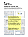
Export Using the Fusion GUI
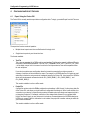
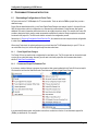
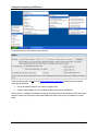
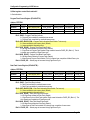
The Fusion GUI is normally used to export device configuration data. To begin, you select Export from the File menu:
The export tool has two modes of operation:
·
Multiple format: export more than one file/format with a single click.
·
Single format: export only one format at a time.
The formats available:
·
Text File
Tab or comma separated list of PMBus settings and readings. This file can be opened by Microsoft Excel or
a text editor. Most PMBus parameters – such as VOUT_COMMAND, READ_VOUT, and IOUT_CAL_GAIN
– will be listed, one per line. In the case of a multi-rail or multi-phase device, there will be separate entries
for each rail/phase.
If your device contains some configuration items that cannot be presented by a single command, a
summary of said item will be included in the export. For example, on UCD92xx devices CLA gains are read
and written to the device using a series of commands issued by the Fusion GUI. A text export of a UCD92xx
device will include pseudo command entries for CLA_GAINS_BANK_0, CLA_GAINS_BANK_1, and
CLA_GAINS_BANK_2.
This mode is available in online or offline mode.
·
Project File
A project file contains a device's PMBus configuration and readings in XML format. It is the primary data file
of the Fusion GUI, and allows you to edit a device's configuration and design in 'offline' mode: without a live
connection to your device. A project file also contains information about your design and sequencing that is
not stored on the device. For example, a definition of the voltage divider network on your system board.
Unlike File->Save Project, you can choose not to include non-command data such as UCD92xx designs or
UCD90xx pin names. When this information is not included, the project file is smaller and may be easier for
you to review/understand.
This mode is available in online or offline mode.
Texas Instruments
Page 7
Configuration Programming of UCD Devices
·
Data Flash File
This export format will read the data flash from the device and save it in S-Record or Intel Hex format. Other
modes, such as project and text file modes, export the current RAM configuration. This mode will export the
data flash configuration. See section 9.1, Exporting Configuration Data Flash Hex File.
This mode is only available in online mode.
·
Program + Data Flash File
This export will read the program and data flash from the device and save it in S-Record or Intel Hex format.
You can download the program+data flash through any of the Fusion tools that download "firmware", where
the Fusion tools define a firmware image as a single file containing program flash and optionally data flash.
Only authorized personnel can export program flash, and this tool is password protected. This mode is only
available in online mode.
·
Data Flash SVF/JTAG
This export format will read the device's data flash from the device and save it in Serial Vector Format
(SVF). SVF is a vendor-independent way of representing JTAG test patterns. The SVF file will contain the
patterns necessary to write your device's configuration. See section 6.3, Downloading a Configuration via
JTAG.
This mode is only available for devices that support JTAG. This is only available in online mode.
·
Program + Data Flash SVF/JTAG
This export format will read the program flash and optionally data flash from the device and save it in Serial
Vector Format (SVF). SVF is a vendor-independent way of representing JTAG test patterns. The SVF file
will contain the patterns necessary to write the device's program and optionally data flash.
This mode is only available for devices that support JTAG. This is only available in online mode.
·
PMBus Script
This will save a “script” detailing the writes necessary to write your current configuration to a device. Writes
are done in terms of standard SMBus commands (WriteByte, WriteWord, and WriteBlock) or I2C WriteBlock.
This can be easily translated to other environments. See section 6.4.3, Microcontroller Writes Full
Configuration via PMBus and section 6.4.4, Microcontroller Writes Partial Configuration via PMBus.
This mode is available in online or offline mode.
·
Data Flash Script
This export will read the data flash from the device and save a script that can be used by a microcontroller
or other device to download data flash to the device. See section 6.4.2, SMBus / I2C Script Overview.
This mode is only available in online mode.
·
Firmware Upgrade Script
This export will read the program and data flash from the device and save a script that can be used by a
microcontroller or other device to download program and data flash to the device. While UCD devices
firmware can be upgraded, Texas Instruments does not expect this to be generally done nor necessary.
Only authorized personnel can export program flash, and this tool is password protected. This mode is only
available in online mode.
Texas Instruments
Page 8
Configuration Programming of UCD Devices
4.2
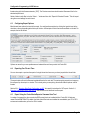
Exporting to Multiple File Formats
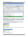
To initiate a multiple format export, select the tab shown below:
You then click the checkboxes next to formats that you want to export. For example, even if you are doing a data
flash export, it is recommended that you also export your device configuration to a project file and text file at the
same time, for archiving and debug.
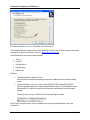
Note that the filename is not a fixed filename. It uses special “macros” to dynamically create a filename. This is
primarily needed because the export multiple format mode will write more than one file. You can changed the
filename template to suit your project naming conventions; however, it is recommended you keep the {PN}, {PKG},
and {DA} “macros”. In the example above, “210434-02” is a part identifier to be assigned to the programmed IC. You
also should keep the {EF} macro if you are exporting multiple formats. It will be used to differentiate between export
Texas Instruments
Page 9
Configuration Programming of UCD Devices
formats along with the filename extension, {EXT}. The Preview area shows what the actual filename will be for the
selected export format.
Select a folder to write files to via the “Select …” button and then click “Export All Checked Formats.” This will export
using the current settings for each format.
4.3
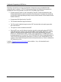
Configuring Export Options
Most formats have options that control the export. You configure these options by clicking the hyperlink next to the
checkbox or the corresponding tab at the top of the form. A description of the format is also available on this tab. For
example, the text file format:
Options are saved to your user preferences and restored the next time you start the Fusion GUI.
4.4
Exporting One File at a Time
You can also export or preview the export of a single format at a time once you have jumped to the format’s tab:
The export option will use the filename template defined on the main tab. The preview option exports to a temporary
file and opens up the output in a window. This is handy when you are poking around with different options and file
formats.
Section 6.3.4, Exporting Data Flash Configuration as SVF, lists specific instructions for SVF export. Section 9.1,
Exporting Configuration Data Flash Hex File, has instructions for data flash hex file export.
4.5
Export Using the FusionDeviceExporter Command Line Tool
A number of command line (aka console aka DOS prompt) tools are bundled with the Fusion GUI. All tools are
named FusionSOMETHING. By default, the folder where the tools were installed to was added to your PC’s PATH
environment variable when you ran the GUI’s installer:
Texas Instruments
Page 10
Configuration Programming of UCD Devices
If this was not checked, you can re-run the installer and check this option.
The FusionDeviceExporter command line tool that is bundled with the Fusion GUI can export a subset of the formats
supported by the export tool described in section 4.1, Export Using the Fusion GUI.
FusionDeviceExporter can export the following formats:
·
Text file
·
Project file
·
Data flash hex file
·
Data flash script
·
PMBus script
Examples:
·
FusionDeviceExporter --address 126 –text
Dumps the device configuration and readings for the device at address 126 to the console (standard
output).
·
FusionDeviceExporter --scan --text --project --outfile '{PN}-{PKG} {DV} Address {DA} {EF}.{EXT}'
Exports configuration/readings for all supported devices found on the bus. Text and project file formats
will be exported. The output will be saved to two different files, each defined by the outfile template
specified.
For example, after running on a UCD90124, the following files might be created:
Like all Fusion command line tools, you can get detailed help by typing FusionDeviceExporter --help on the
command line.
Texas Instruments
Page 11
Configuration Programming of UCD Devices
5
DATA FLASH CONSIDERATIONS
Data flash refers to a section of the device’s EEPROM that holds non-volatile device configuration and other
operational data. Many UCD devices store more than just configuration information in data flash. For example,
UCD92xx and UCD90xx devices log information about faults that occur to data flash.
Each device (UCD9240-64, UCD9240-80, UCD9248, UCD90120, etc.) and possibly the specific firmware release for
a given device (UCD9248-80-5.6.0.1123, etc.) will have a “memory map” that defines where in the flash the data that
the device maintains is stored. As a device’s firmware is updated, the location in data flash where a particular piece
of data is stored may change. For example, say that the data flash layout for a device looks like this:
·
·
Address 0x18800: Fault logging information
o
Address 0x18800: Rail #1 faults
o
Address 0x18802: Rail #2 faults
o
Etc.
Address 0x18A00: Configuration information
o
Address 0x18A00: VOUT_COMMAND rail #1
o
Address 0x18A02: VOUT_OV_FAULT_LIMIT rail #1
o
Etc.
But what if, on a new firmware release, the amount of data that was saved in the fault logged was changed? Or the
“memory map” of configuration data was changed, perhaps to optimize the firmware in some way? In either case, the
data flash between firmware releases would no longer be compatible.
Another complication is that devices often store information in non-volatile and volatile memory differently than they
are passed back and forth via PMBus. For example, the GUI writes VOUT_COMMAND as a 16 bit signed mantissa.
The exponent is configured through another command, VOUT_CONFIG. The device does not store this in RAM or
flash in the PMBus format. It stores it in a fixed point (Q math) representation. This is only one example of the PMBus
® device translation. Different commands use other encoding schemes, and these schemes can change between
major releases.
PMBus hides the memory map and command encoding issues by providing a command-based front end for reading
and writing a device’s configuration. In the case of TI UCD devices, special “manufacturing specific” (custom) PMBus
commands are also used to read and reset fault logs and other flash-based logged data.
The Fusion GUI normally reads and writes configuration via PMBus and thus avoids these issues. All the GUI needs
to worry about between firmware releases is whether a command has been added, removed, or data format modified
between firmware releases. The underlying memory map of the device is not tracked by the GUI.
Data flash-based configuration is much more brute force. It is ultimately a bit-by-bit copy of a source data flash image
to a target device. Great care must therefore be taken to ensure that the firmware loaded on the “source” – the
device that will be used to generate the configuration export – matches the firmware loaded on the “target” device.
Because of this, if your target device version changes, you should normally create a new configuration export
from a live device.
Texas Instruments
Page 12
Configuration Programming of UCD Devices
Depending on the method you are using to write data flash, the target device may be validated before flash
programming starts. For example, a JTAG SVF data flash programming file will validate that the target device is
compatible with the SVF being executed. In the case of SVF, the validation works as follows:
·
Engineer connects to a device in “online” mode with the Fusion GUI. The device should have the same
firmware loaded that will be on the ICs received from Texas Instruments. For example, if the customer had
previously been developing/validating their design with pre-production firmware, the final firmware should be
loaded on lab devices.
·
Engineer selects File->Export from the Fusion GUI.
·
The GUI reads the data flash image from the device.
·
The GUI converts this data flash image to a series of SVF instructions that can be used to program data
flash on other devices.
·
The engineer or contract manufacturer tests the SVF.
·
When the SVF is run, one of the first tasks it performs is to read the contents of the device’s DEVICE_ID
register. DEVICE_ID is a read-only Texas Instruments PMBus command (MFR_SPECIFIC_45, command
code 0xFD, read block) that returns the device part, firmware version, and release date. An example
DEVICE_ID is “UCD9240-64|3.25.0.8662”. The GUI normally reads DEVICE_ID via PMBus when it scans
for devices during startup. In the case of SVF, the SVF will read DEVICE_ID from program flash memory via
JTAG. DEVICE_ID is always stored at a fixed location on TI devices. The SVF will read DEVICE_ID and
compare it to what it expects the target to be (the device the export was done on). If there is a mismatch, the
SVF will abort with an error.
In section 6, Programming Options and Instructions, device validation – if any – will be described for each
programming option.
Texas Instruments
Page 13
Configuration Programming of UCD Devices
6
6.1
PROGRAMMING OPTIONS AND INSTRUCTIONS
Downloading a Configuration via Fusion Tools
All Fusion tools use the TI USB adapter for I2C communication. Tools can write via PMBus (project files) or write a
data flash image.
Project files are described more fully in the Fusion Digital Power Designer user manual, section 9. A project file is an
XML file that contains a device’s configuration on a command-by-command basis. Project files may also contain
additional GUI-centric information about a device that is not actually stored on a device. For example, the Fusion GUI
provides a design tool that is used to create compensation coefficients for a device. Design components are criteria
are stored in the project file. This GUI-centric data is not used in the configuration process.
See section 9.1, Exporting Configuration Data Flash Hex File, for instructions on how to export a device configuration
to a data flash hex file.
When using Fusion tools, for optimal performance you should hook the TI USB adapter directly to your PC. Do not
use a hub/dock of any kind, as this will significantly slow down write times.
6.1.1
Fusion Digital Power Designer
The Fusion GUI can be used to write a configuration for small batch runs. The File->Import tool can be used to import
a project file or a data flash image. Normally you will want to stick with project files for the reasons described in
section 5, Data Flash Considerations.
6.1.2
Firmware and Project File Download Tool
If you have a number of devices to program, this simple tool that comes bundled with the Fusion GUI may be helpful.
You launch the tool from the Start Menu under Texas Instruments Fusion Digital Power Designer:
It can download firmware and/or configuration to more than one device on the bus. It can download a project file
(PMBus) or data flash file. For example:
Texas Instruments
Page 14
Configuration Programming of UCD Devices
Because only configuration is being downloaded, firmware and IC information did not need to be filled in. Only the
PMBus address, configuration mode, and configuration file need to be filled in before clicking the Start button.
Your settings are remembered when you exit and restored the next time you run the tool.
6.1.3
FusionConfigWriter Command Line Tool
The Fusion GUI comes bundled with a number of command line (aka console, batch mode) tools. The
FusionConfigWriter tool can be used to download a project or data flash file to a device. This tool would be helpful if
you have an existing manufacturing test executive such as National Instruments TestStand and want to integrate
UCD configuration into your process flow.
The options of these tools are similar to the Firmware and Project File Download Tool described above. If writing a
project file:
FusionConfigWriter [ scan options ] --project --infile project-file
[ --skip-operation --force-write --project-file-warnings-ok --device-exact-version version --quiet ]
The --skip-operation, --force-write, --project-file-warnings, and –quiet arguments are optional. Scan options is a place
holder for arguments used to define the device you are targeting. While you can only write to a single device in each
call to FusionConfigWriter, you can invoke the program any number of times if you have multiple UCD devices on the
bus. For example:
FusionConfigWriter --address 75 --project --infile ML605A_addr75_300uF_r8.xml
FusionConfigWriter --address 101 --project --infile ML605B_addr101_300uF_r8.xml
Texas Instruments
Page 15
Configuration Programming of UCD Devices
The syntax when writing a data flash image is similar:
FusionConfigWriter [ scan options ] --dflash --infile eeprom-file [ --device-exact-version version --quiet ]
The --device-exact-version version argument is recommended when writing data flash if you are deploying this as
part of a larger manufacturing process. When specified, if the device that is targeted does not match the exact
firmware version specified, the tool will exit with an error.
For example:
FusionConfigWriter --address 75 --device-exact-version 3.25.0.8663 --dflash --infile UCD9240-64-3.25.0.8662Address75-DataFlash.hex
FusionConfigWriter --address 101 --device-exact-version 3.25.0.8663 --dflash --infile UCD9240-64-3.25.0.8662Address101-DataFlash.hex
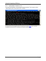
Example output in data flash mode:
Sending the device to ROM mode ...
Waiting for ROM mode via ROM version fetch ...
Device in ROM mode; UCD3000 ROM v0.2; IC v0.2
Mass erasing data flash
Writing data flash ...
Wrote data flash without error
Verifying data flash through read back ...
Reading data flash ...
Data flash verified!
Recreating program flash checksum ...
ROM is calculating program flash checksum ...
Reading last segment of existing program flash ...
Erasing last segment of program flash ...
Downloading new segment of program flash ...
Program flash update 100% successful; program will run on device power-up
Executing program flash and waiting for device to come online ...
Device in program mode after 250.8208 msec wait, DEVICE_ID is 'UCD9240-64|3.25.0.8662|081105'
Note there are two ways to specify devices to target on the bus. If you have multiple devices on the bus, then
--address must be used as shown above. If you have only a single device, you could use the --scan option instead to
have the tool use whatever device is found on the bus. This might be useful in a single device setup where the
address is not fixed.
The FusionPMBusScan tool can be used to list what devices are on the bus. For example:
FusionPMBusScan
Starting scan for SAA #1 from 1-11,13-127
Found device @ address 88d: ReadBlock DEVICE_ID [0xFD] retured UCD3000ISO1|0.0.0|110609
[0x5543443330303049534F317C302E302E307C313130363039 ]
Found device @ address 103d: ReadBlock DEVICE_ID [0xFD] retured UCD9224-48|5.6.0.11224|090922
[0x554344393232342D34387C352E362E302E31313232347C30393039323200 ]
Found 2 device(s)
Texas Instruments
Page 16
Configuration Programming of UCD Devices
All Fusion command line tools return exit status code of 0 on success and non-0 on failure. This is a DOS/UN*X
convention. So you can check for this return status code and simply log the results.
Full documentation of the tool is available by launching a DOS (or similar shell) window and typing
FusionConfigWriter --help.
6.1.4
Fusion Manufacturing GUI (MFR GUI)
The MFR GUI provides a framework to perform a variety of manufacturing activities on Texas Instruments UCD
device(s) in a lab or factory setting. You can create “scripts” that can:
·
Download firmware
·
Download configuration (project file or data flash)
·
Write serial numbers and date
·
Calibrate device (manual or instrumented)
·
Test device
·
Other: open API for customer to add their own custom processes
The MFR GUI is driven off of a special XML file called a “manufacturing script.” It defines the devices in your system
and the activities – called tasks – you want to perform on each device. Tasks are listed in order that they should be
executed. If a task fails, the script will stop for the device. Tasks can also have configurable retry. If you are familiar
with TestStand, think of the MFR GUI as a mini-TestStand, highly optimized for UCD devices.
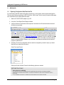
The MFR GUI has two distinct operating modes: script editing and script running. Script editing is a one time or
maintenance activity where you define the tasks that will be performed on your devices. After you have launched the
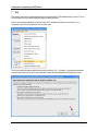
MFR GUI from the Start Menu, you should enter the “Admin” mode to create a new script:
The password is “texas”. A script can be created/edited in Admin mode only. This password prevents an “operator” –
someone running the script with limited knowledge of the tool/device(s) – from accidently changing the script.
For the purposes of this document, two very simple MFR GUI scripts will be created to download configuration to a
device. One script will use project files. The other will use data flash images. To jump start the script creation
process, click the “New Wizard” icon in the toolbar:
Texas Instruments
Page 17
Configuration Programming of UCD Devices
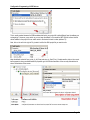
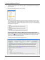
Select the “Configure_With_Project_File” template and click the Create button. This will yield this simple script:
Scripts are organized by device, then by activity, and then by task. In the case of the wizard, a place holder device
was defined. Click the “Discovery@6” node in the tree. You’ll notice that the properties area to the right changes after
you select the device. You define properties about the selected node in this area. For example, to target a UCD9240
at address 75:
Next, click on the “Configure_and_Validate” node. Click on cell to the right of devce_choice – SAME_AS_DEVICE is
the default – and change the selection to “First address in project file with the same device Part_ID” and click OK:
Texas Instruments
Page 18
Configuration Programming of UCD Devices
This is usually needed because the PMBus address defined in your project file is often different from the address you
are targeting. If, however, yours match up, you can keep the default. In this mode the MFR GUI will enforce that the
device address in the project file is an exact match to the device this task is under (address 75).
Next, click on the cell to the right of “file_location” and find the XML project file you want to write:
Keep the default values for force_write_of_all (False) and store_to_flash (True). Context sensitive help on the current
task argument is always available below the properties grid. And full documentation of the currently selected task is
shown at the bottom of the screen:
Texas Instruments
Page 19
Configuration Programming of UCD Devices
Next, click the “Save -> Run” button on the toolbar:
You’ll be prompted to select a location for your MFR GUI “script.” Note that the extension is the same as project files:
.xml. After the save is done, the MFR GUI will jump to the script runner tab. Click the Start button to execute the
script. The MFR GUI shows PASS/FAIL via a banner at the bottom of the run tab:
When you are ready to program another part, you do not need to quit the MFR GUI. Simply swap out devices and
click the Start button again. The log area will be cleared and the script will restart from the top, including standard
device discovery to verify that a device is present.
Detailed log files are saved for each script “run”. See the MFR GUI user manual for complete instructions and details.
The MFR GUI can do much more than download configuration files.
If you need to program a data flash image instead, select the “Configure_With_Data_Flash_File” template in the
“New Wizard”. Follow the steps above to set the device part/address. Then click the “Data_Flash_Download” task
and select the data flash hex file to program. Optionally, you can have the MFR GUI validate that the firmware
version of the target device is a specific version. One easy way to determine this version is to look at the filename of
the data flash hex file.
If you used the default and recommended file name template when you exported your data flash image in the Fusion
GUI, the filename will contain the firmware version that the data flash was exported from. In the following example
the data flash file was exported from firmware version 3.25.0.8662:
Texas Instruments
Page 20
Configuration Programming of UCD Devices
6.2
Downloading a Configuration Using a Dedicated EEPROM Programmer
You should inquire about support for your target device as soon as possible. Each EEPROM programming vendor
must add support for UCD devices. Some will add generic support, which will work for almost any UCD3000-based
device (for example, UCD9240 or UCD90120). Others need to add support for each unique TI device. Section 9.3,
Gang Programmer Notes, lists distributors and vendors that TI has worked with to add programming support for UCD
devices.
You should perform a sample programming run as early as possible, even before a final device configuration is
locked down.
Follow the instructions in section 9.1, Exporting Configuration Data Flash Hex File, to create a hex file for your
programming vendor.
Texas Instruments
Page 21
Configuration Programming of UCD Devices
6.3
Downloading a Configuration via JTAG
JTAG (Joint Test Action Group) is the common name for the IEEE 1149.1 Standard Test Access Port and BoundaryScan Architecture. In UCD devices JTAG provides debug facilities for device development within TI and EEPROM
download by TI customers.
The Fusion toolset is capable of generating SVF that can be used to configure the device via JTAG. While, in theory,
SVF should provide a solution that will port to any given JTAG programming toolset, the reality is that the SVF syntax
definition is vulnerable to multiple interpretations. Fusion provides options for generating different forms of the SVF
that are compatible with several different JTAG toolsets. Each customer must confirm that they can reliably
configure the device via JTAG with their programming tools. This can be done by obtaining the appropriate EVM
and samples of the device from Texas Instruments.
JTAG programming may occasionally fail on UCD devices due to an internal clocking issue. This issue is
limited to the JTAG interface and does not affect any form of normal operation. The failure is not predictable
and may not occur in all configurations. If a failure occurs, the customer should reset the device and attempt
running the SVF a second time.
6.3.1
System Board Requirements
The JTAG pins (TMS, TDI, TDO, TCK) from the device must be accessible to the JTAG controller. The control and
data lines (TMS, TDI, TDO) should be pulled high on the board.
If the device has a TRCK (return clock) pin and the JTAG controller supports that pin as well, the two should be
connected. If the JTAG controller has a TRCK pin, but the device does not, the TRCK signal should be connected to
the TCK signal on the board.
The nTRST signal should be high with programming the device via JTAG. It should be low for normal operation.
6.3.2
Overview of SVF
SVF (Serial Vector Format) is an ASCII-based standard for expressing test patterns that represent the stimulus,
expected response, and mask data for JTAG-based configuration. SVF was selected because it allows Texas
Instruments to create vendor-independent JTAG configuration patterns that are transportable across a wide selection
of programming software and equipment.
For additional information, please refer to IEEE 1149.1 Testability Primer.
6.3.3
Differences Between IC Packages
Most UCD devices support JTAG. Typically, the PMBus address pins must be shorted to ground to enable the JTAG
interface. Some exceptions are noted here:
·
It is not necessary to short the PMBus address pins to ground when using the UCD9248
·
Any 40 pin package does not support JTAG
·
UCD3028 does not support JTAG
·
The UCD device can be set to PMBus address 126 to leave JTAG always enabled. Note – using this
method will disable use of the JTAG pins as GPIO in devices that support multiplexing of these pins. You
must also ensure that no other device on the same PMBus could end up at address 126. For example, do
not use this method when there are multiple UCD devices on the same PMBus.
Texas Instruments
Page 22
Configuration Programming of UCD Devices
6.3.4
Exporting Data Flash Configuration as SVF
The Fusion GUI’s File->Export tool is used to generate an SVF file. You should use the “Data Flash SVF/JTAG”
export mode:
The default options are:
The SVF file will verify that the device it is trying to program is compatible with the data flash image. When the SVF is
executed, it will read the target device's DEVICE_ID and compare it against what you have selected above. We
recommend you stick with the default, exact DEVICE_ID match. This will require that the exact same device/firmware
version that you are currently connected to will be your programming target. You should only select one of the other
choices if you have contacted Texas Instruments and verified that the memory map for your target device is
compatible with the attached source device.
It is recommend you export your configuration as a project file and data flash hex file at the same time you export
SVF. See section 4.2, Exporting to Multiple File Formats, for additional information. While the Fusion tools do not
support importing SVF, they can import a data flash file, allowing write to data flash directly.
6.3.5
SVF Flow
The SVF performs the following steps when downloading configuration data:
·
Erase data flash
Texas Instruments
Page 23
Configuration Programming of UCD Devices
·
Write data flash
·
Verify data flash
6.3.6
BSDL File
A BSDL (Boundary Scan Description Language) file is available for all UCD30xx-based devices that support JTAG.
The file, ucd30xx.bsdl, is located in the misc folder within the Fusion GUI program directory. This is normally
C:\Program Files\Texas Instruments Fusion Digital Power Designer\misc.
6.3.7
Supported TCK Frequencies
TCK frequencies up to 5 MHz have been tested using ASSET ScanWorks on a RIC-1000. 4 MHz has been tested on
JTAG Technologies boundary scan controllers. For other programmers, you should start at 1 MHz and increase clock
frequency until you experience programming errors. Thoroughly test the selected frequency, and consider decreasing
the clock speed further to allow for variation in your manufacturing environment.
6.3.8
List of Tested Programmers
The following controllers have been tested and used to configure a device via JTAG (in alphabetical order):
·
ASSET
Tested against USB-100 and RIC-1000 programmers.
·
Corelis
Tested against all currently supported Corelis JTAG controllers, as of August 2010.
·
GOEPEL Electronic
Tested against SFX/USL1149-B controller. All SCANFLEX and ScanBooster controllers will support UCD
devices. Requires SYSTEM CASCON software version 4.5.3c or higher.
·
JTAG Technologies
Tested with JT 37x7 / TSI boundary scan controller. Other solutions should work as well.
·
Teradyne
The SVF must be converted to a JTAG control language used by Teradyne. The conversion tool is called
ISP 3.0.0. This is a tool written and maintained by Teradyne. SVF produced by the Fusion GUI has been
tested and confirmed to work on the 2287LX test system, but should work on any of the Teradyne Test
Station systems or the older GenRad 228X systems. While not tested, Teradyne Test Station SE and
Spectrum systems should also accept converted files.
·
Other In-Circuit Test (ICT) equipment
Most ICT equipment requires conversion from SVF to a proprietary format. Contact your ICT vendor for
assistance.
6.3.9
Troubleshooting
If you are experiencing problems programming via JTAG, please review these troubleshooting hints and steps:
·
Have you shorted the address lines to ground during JTAG programming?
·
Is the nTRST signal high during JTAG programming?
Texas Instruments
Page 24
Configuration Programming of UCD Devices
·
6.3.10
If the TRCK is used by the JTAG controller, is it connected to the TRCK signal on the device or the TCK
signal?
Additional Information & Help
JTAG vendors should reference Appendix 8.6, Miscellaneous JTAG Questions, for additional information about
device memory. Customers who need JTAG programming assistance should contact their TI representative.
Texas Instruments
Page 25
Configuration Programming of UCD Devices
6.4
Downloading Configuration Data Using a Microcontroller
Your system board microcontroller (µc) could download a full or partial configuration to a device. This programming
would be performed via I2C. The µc could download one of the following:
·
A full configuration via data flash. More recent devices like the UCD90160, UCD9222, and UCD9244 permit
update of the device’s data flash while the device is operating normally. The device is reset to load the new
configuration when download is complete. Other UCD devices require the device be sent to ROM mode
before the data flash can be written. Thus, normal device operation is not possible in these devices during
data flash download. Section 6.4.2 lists which devices support Normal Mode data flash download and which
require ROM Mode download.
·
A full configuration via PMBus. The µc will assume the device configuration is in an unknown state or a
factory virgin state. The full configuration will be written to the device through standard PMBus commands.
·
A partial configuration via PMBus. Your µc assumes that some baseline configuration is in the device and
writes an “update” to the device using PMBus commands.
It is recommended you read this entire section to understand the pros and cons of each method.
There are two approaches when developing your configuration download scheme:
·
Export a data flash “script” files using the GUI. A script file lists each SMBus/I2C step that is required to
download data flash to the device. You will need to develop a “script” execution engine for your
microcontroller that parses the script file and converts it to appropriate SMBus/I2C calls. This is explained in
detail in the sections that follow.
·
Export a data flash hex file using the GUI. Create a custom programming solution on your microcontroller
that accepts hex input and writes to the device using the general recipe described in this section. Sample
“C” source code that was developed to run on the Texas Instruments’ Stellaris LM3S811 device (ARM
Cortex-M3 based) is available. Download from http://softwaredl.ti.com/analog/analog_public_sw/fusion/UCD9xxx-UCD3xxx-Programming-Example-C-Code.zip.
The script format is the preferred approach, because at any time TI can update the script logic with no changes
required on the microcontroller end. Script exports can also be generated for the following activities:
·
Downloading a full or partial configuration using PMBus
·
Upgrading a device’s firmware
Thus, a common script execution engine developed for your microcontroller can be used for a variety of UCD
download activities, including for future devices.
6.4.1
SMBus / I2C Script Overview
Texas Instruments has developed a generic, platform independent method of describing the steps necessary to
perform some of the above actions. This is dubbed a “script” and can take one of two forms:
·
SMBus Script: describe a series of bus transactions in terms of the high-level System Management Bus
(SMBus) protocol. This means “Send Byte”, “Write Byte”, etc.
·
I2C Script: describes bus transactions in terms of the lower level I2C protocol.
Texas Instruments
Page 26
Configuration Programming of UCD Devices
Which you will use will depend on your microcontroller firmware development environment and APIs. You may
already have an API stack that abstracts communication with devices like a UCD9240 in terms of SMBus. For
example, to set the OPERATION command to 0x80 (On, No Margin) would mean issuing a Write Byte to command
code 0x01 with data byte 0x80. And of course an address of the device is needed. A microcontroller SMBus API
might define a function such as:
bool write_byte(byte address, byte cmd_code, byte data)
{
…
}
So sending the sample OPERATION command to address 12d would mean calling:
write_byte(0x0C, 0x01, 0x80);
Not shown here is specification of a Packet Error Check (PEC) byte. This might be an optional argument or some
type of global construct: i.e. always attach PEC byte to writes for devices on the bus. A sample “C” function that
calculates a PEC byte is in appendix 9.9.
Any SMBus stack will ultimately communicate with the device in terms of I2C reads and writes. SMBus is simply a
protocol layer on top of I2C. I2C packs the addressing information, command code, data, and optional PEC byte into a
block of data. A bit is used to determine whether the request is a read or write.
In our example above, the OPERATION write byte with PEC appended would translate to an I2C write of:
Address, R/W Bit
Command Code
Data Byte
PEC Byte
0x18
0x01
0x80
0x6F
Scripts are created using the File->Export tool. All script export formats have the following options:
Script Style
Whether to output a script that performs writes in terms of high-level SMBus or low-level
I2C.
Store RAM to Flash?
Checking this box will automatically perform a STORE_DEFAULT_ALL before every
firmware script export. If this is not checked, any changes you recently made to your config
but did not write to non-volatile memory (dflash) will not be included in the script.
PEC
Only used for the I2C format. Checking this will include the Packed Error Code byte in each
I2C write.
File Format
Choose between Comma Separated Value (CSV) and tab separated formats.
Hex Format
A variety of hex formats are supported.
Comment Style
A number of comment styles are supported. A comment proceeds each major section of
the script, such as “Downloading data flash ...”
How to Handle Multiple
Data Bytes
How to format the data field for an SMBus or I2C write command. For example, WriteBlock
accepts an array of 1+ bytes. By default – “compact together into one field” – this block of
data is concatenated together in one field using the Hex Format style. As an alternative,
you can select “break apart into separate fields” to break out the data bytes into different
fields (columns).
Security
For devices that support Texas Instruments enhanced command security, you can chose
to write a security password to data flash before doing the export. See the Security section
Texas Instruments
Page 27
Configuration Programming of UCD Devices
of the Fusion Digital Power Designer User’s Guide for more information about security.
Embedded Device Address
This option allows you to create a script that targets the device address used “in the field,”
should it differ from the device you are currently attached to.
Add block length byte to
read block and write block
commands in SMBus mode
Earlier versions of the GUI did not add block length to block reads/writes, and your parser
would have to compute them. Export now includes block length by default. The option can
be unchecked to create files in the old format.
Seesection 4, Configuration Export Overview, for additional tips on using the export tool.
6.4.2
Microcontroller Writes Data Flash
Some UCD devices do not support data flash download while in normal operating mode. These devices must be sent
to ROM mode to download a new data flash image. When in ROM mode, the device is not executing its normal
firmware program and will not perform its primary function(s): power regulation, sequencing, monitoring, etc. The
device will also not respond to system stimulus, such as a GPI state change or a fault condition. Thus, if your
microcontroller or other critical component is powered by a rail on the UCD device, this configuration update process
is not appropriate. See section 6.4.3 Microcontroller Writes Full Configuration via PMBus and section 6.4.4
Microcontroller Writes Partial Configuration via PMBus for alternatives that allow in-process configuration update on
these devices.
Consult section 9.2, Firmware Versions, Program Flash Checksums, and Programming Modes for Released Devices,
to determine which data flash download scheme is supported by your device.
The “Data Flash Script” export format can be used to generate the recipe needed to write data flash to a device. The
Export tool is launched from the Fusion GUI’s File menu, under “Export …” The data flash script format is in the
upper right corner of the form:
The data flash config script can only be generated in online mode. All the usual caveats about firmware versioning
apply. The GUI will read the device’s current configuration from EEPROM and create a “script” detailing the steps
your microcontroller must perform to update data flash. The GUI will automatically select the appropriate scheme –
Normal Mode or ROM Mode – based on the device that is attached.
6.4.2.1
Microcontroller Writes Data Flash, Normal Mode Scheme
In this scheme, a new data flash image is written to the device while it continues to operate. The general recipe for
writing data flash using this scheme is:
·
Verify the target device is the correct part and at the expected firmware revision
·
Disable data flash write protection (normally the device does not allow data flash to be written to).
·
Erase data flash.
Texas Instruments
Page 28
Configuration Programming of UCD Devices
·
Write data flash.
·
Verify data flash (read back).
·
Reset the device.
·
Verify that the device is running again (DEVICE_ID or other check).
·
Erase data flash logs.
The device will operate normally during the data flash download with one exception: data flash logging will not occur.
For example, if your device supports fault logging, is configured to log a certain fault, and that fault occurs, the device
will not log the fault to data flash. It will, however, continue to update status registers such as STATUS_VOUT.
An abbreviated example script is in section 9.6, Data Flash Download Script Example – Normal Mode. The full recipe
for writing data flash in normal mode is described in more detail in section 9.5, Detailed Recipe for Device Writes
Data Flash, Normal Mode Scheme.
6.4.2.2
Microcontroller Writes Data Flash, ROM Mode Scheme
In this scheme, the device must be sent to ROM mode to write data flash. When in ROM mode, the device will not
perform normal operations, such as power conversion, monitoring, or sequencing. The general recipe of writing to
data flash is:
·
Verify the target device is the correct part and at the expected firmware revision
·
Send the device to ROM mode.
·
Erase data flash.
·
Write data flash.
·
Verify data flash (read back).
·
Recreate the program flash checksum.
·
Verify the program flash by comparing ROM calculated checksum against the checksum that was written.
·
Issue a ROM command to execute the device program.
·
Verify that the device is running again (DEVICE_ID or other check).
·
Erase data flash logs.
The sequence is complicated because of the need to send the device to ROM mode.
The firmware gets the device to ROM mode by clearing the program flash checksum and then resetting the device.
After reset, the device will stay in ROM mode. UCD devices provide a MFR_SPECIFIC PMBus command to do this,
ENABLE_ROM. When in ROM mode, the device responds at a hard coded address, 11d. You should therefore not
use address 11 for any other devices on the same bus. When data flash write is completed, the program flash
checksum will need to be recreated. Because flash memory can only be written when it is in an “erased” state, the
script will erase an entire segment of program flash and then recreate it.
The UCD ROM requires a PEC byte on writes and always sends a PEC byte on reads. While devices in program
mode (UCD9240, UCD9240, UCD90120, etc) do not require PEC, it is recommended if your I2C bus has excessive
noise or other limitations. A sample “C” function that calculates a PEC byte is in appendix 9.9.
An abbreviated example script for data flash download via ROM is in section 9.5, Data Flash Download Script
Example – ROM Mode.
Texas Instruments
Page 29
Configuration Programming of UCD Devices
6.4.3
Microcontroller Writes Full Configuration via PMBus
The Fusion GUI loads project files by writing to the device using PMBus commands. Your µc could do the same. The
PMBus Script export format is used to generate the series of PMBus writes necessary to configure a device. The
script generated is very “dumb”: it assumes the device is in a completely unconfigured state. For UCD92xx devices,
the script will even reset the device, as this is required after setting the rail/phase configuration of the device.
A PMBus config script for a UCD9224 with two rails follows is included in section 9.8, UCD9224 PMBus Config Script
Example. A UCD90124 example is listed in section 9.8.2, UCD90124 PMBus Config Script Example. PMBus scripts
can be generated online or offline.
6.4.4
Microcontroller Writes Partial Configuration via PMBus
While updating a configuration in the field using the “full” configuration scripts described in section 6.4.2 and 6.4.3 is
possible, with UCD92xx parts the device must be taken offline for a short period during the write sequence (to
perform a soft reset). It is also likely that only a small number of parameters need to be updated. Thus, you may want
to use a subset of the script export when writing a configuration update via your µc.
It is recommended you use one of the MFR_ commands to store a unique configuration identifier in each UCD
device. For example, MFR_REVISION may have a configuration ID embedded within it, such as REVC. The µc
firmware can use this to determine whether it needs to upgrade a configuration on a UCD device. The µc could store
a “script” that would take the device from REVA or REVB to REVC.
The GUI does not include any tools to assist in generating such a configuration upgrade script. But generating a
script for REVA and REVC, then doing a “diff” between the two will provide clues on what the upgrade script should
do. KDiff3 is an open-source, free file compare tool you can use.
6.4.5
Testing the Export Using the Script Runner Tool
You can run scripts three ways:
·
The File->Import wizard has a script option
·
Use the stand alone Script Runner tool that is bundled in the Fusion GUI
·
Use the FusionScriptRunner command line tool
These tools will execute any script matching one of the SMBus/I2C script formats supported by the FileàExport tool.
6.4.5.1
Script Runner GUI Tool
Launch the It is available from the GUI’s Start Menu Tools folder:
Texas Instruments
Page 30
Configuration Programming of UCD Devices
The tool has options to control how the script is executed:
The device address option will not work with ROM mode data flash configuration download scripts, because this
mode uses two addresses:
·
One for the address the device runs on when in program mode
·
A second, fixed at address 11d, for the address the device runs at when in ROM mode
As the script is run, a progress bar indicates how many of the script’s steps have been performed. At the end of script
execution, a log of every script action that was performed will be written to the log area. An example run is shown
below:
Texas Instruments
Page 31
Configuration Programming of UCD Devices
Scripts cannot be cancelled once they have started execution.
Although an I2C script may include a PEC byte, the PEC byte is actually ignored by the Script Runner. This is
because the TI USB adapter handles adding the PEC byte to all SMBus and I2C writes. You can globally turn PEC
mode on and off by adjusting the USB adapter’s settings from the File menu:
Script Runner also has several tools to scan for devices and command devices to jump to and from program/ROM
modes:
Texas Instruments
Page 32
Configuration Programming of UCD Devices
6.4.5.2
FusionScriptRunner Command Line Tool
You can type FusionScriptRunner --help (two dashes) to display documentation. The tool accepts an optional
--address argument similar to the Script Runner GUI. For example:
If you do a lot of work with command line tools, we recommend you review the Cygwin toolset. It provides a
Linux/UNIX-like environment for DOS, including a much-improved command shell.
Texas Instruments
Page 33
Configuration Programming of UCD Devices
7
TIPS
When using Fusion tools, for optimal performance you should hook the TI USB adapter directly to your PC. Do not
use a hub/dock of any kind, as this will significantly slow down write times.
You can clear a device’s data flash through the Fusion GUI to simulate how a device will arrive from TI (unconfigured). Select “Clear Configuration” from the Tools menu:
The GUI will restart after erasing data flash and writing the factory 1010… bit pattern. If you wanted to experiment
with using tools other than the GUI to import data flash, simply Cancel the wizard that will appear after restart:
Texas Instruments
Page 34
Configuration Programming of UCD Devices
8
FREQUENTLY ASKED QUESTIONS (FAQS)
8.1
Why do I need to be connected to a device to export hex or SVF?
Texas Instruments digital power controllers and sequencers use the PMBus protocol to configure devices. This
protocol acts as a middleman between the device’s volatile memory (RAM), non-volatile memory (flash), and the host
(GUI). The GUI writes a device configuration through a series of PMBus commands. For example, output voltage
may be configured by the PMBus VOUT_COMMAND command, while turn on delay is configured by the PMBus
TON_DELAY command.
When the host writes a configuration, it is actually not writing directly to flash memory. It is writing to volatile RAM
memory. The device accepts incoming “write” requests for commands, and maps these to an area in RAM, possibly
translating the configuration data written via PMBus to an internal device-specific format.
Because PMBus command writes are to volatile RAM memory, an engineer can test changes safely. If there is an
error, they can recover their previous configuration by issuing a device reset. When the engineer determines that a
configuration is valid, they can commit the configuration to non-volatile flash memory. This is done by issuing the
special PMBus STORE_DEFAULT_ALL command. The device handles copying parts of RAM to flash memory.
Devices often store information in non-volatile and volatile memory differently than they are passed back and forth via
PMBus. For example, the GUI writes VOUT_COMMAND as a 16 bit signed mantissa. The exponent is configured
through another command, VOUT_CONFIG. The device does not store this in RAM or flash in the PMBus format. It
stores it in a fixed point (Q math) representation.
This is only one example of the PMBus ® device translation. Devices may change what information they store to
flash, where they store it, and what the encoding of that information is between device release cycles. Due to this
complexity, it is not possible for the Fusion tools to translate a project file to a data flash hex or SVF file.
See section 5, Data Flash Considerations, for additional information.
8.2
Do I need to be connected to my system board to export data flash or SVF, or will any board
do?
Normally you can export flash by connecting to any device that has the exact same IC package (pin count) and
firmware version load that will be present at manufacturing. This can be an “open loop” board with a compatible UCD
IC on it, with the production firmware loaded.
For example, if you are targeting a UCD9246 (64 pin) but have a UCD9240-64 open loop board available, you can:
·
Download the production UCD9246 firmware to this board using the Firmware Download Tool
·
Launch the Fusion GUI
·
Import your project file
·
Export data flash
Please contact your Texas Instruments representative if you need an open loop board to assist in programming
activities.
Texas Instruments
Page 35
Configuration Programming of UCD Devices
8.3
Is there a data flash checksum I can read to validate that the flash has been programmed
correctly?
A checksum for the entire contents of data flash cannot be used to validate flash-based configuration programming.
The UCD92xx and UCD90xx devices update data flash as part of their normal operation. For example, both have
facilities to log faults and peak readings to data flash. Once the data flash has been downloaded and the device
resumes normal operation, it is likely that the device will update flash on its own to log new peak readings. Thus, any
data flash checksum calculated would be different from the checksum for the flash image that was downloaded.
Please see FAQ 8.4 and 8.5 for an explanation of internal (not host addressable) data flash checksum(s) that UCD
devices maintain to ensure integrity of data flash. These FAQs also describe how the device responds to corrupt data
flash conditions.
8.4
How does the device validate that its data flash has not been corrupted?
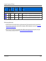
Each device maintains a checksum for the configuration section of data flash. Generically, data flash is segmented in
the following way:
Configuration Data
Logged Faults and
Peaks
Configuration Data
Logged Faults /Peaks
Checksum of
Configuration Data
Unused Data
Flash
Checksum of
Configuration Data
Checksum of Logged
Faults/Peaks
Unused Data Flash
UCD92xx Data Flash
UCD90xx Data Flash
When the device powers up and executes its program, it computes the checksum of the configuration section of data
flash. It compares this to the checksum section. If there is no match, this is an error condition and the device does the
following:
· The device loads a default configuration into operational memory (RAM). This is the configuration that is read
and written via PMBus. This configuration is referred to as the HARDCODED PARMS configuration. The
HARDCODED PARMS config does not have any rails, fans, GPOs, or GPIs defined (UCD92xx and
UCD90xx) nor any monitors or PWMs defined (UCD90xx only). On the UCD92xx, the device will not convert
power because no rails are defined. On the UCD90xx, the device will not perform any monitoring or
sequencing operations because no rails/monitors have been defined.
· The configuration also loads default values for the MFR_XXX commands. For example:
Command
Code
HARDCODED PARMS Value
MFR_DATE
0x9D
YYMMDD
MFR_ID
0x99
MFR_ID
MFR_LOCATION
0x9C
MFR_LOCATION
MFR_MODEL
0x9A
MFR_MODEL
MFR_REVISION
0x9B
MFR_REVISION
MFR_SERIAL
0x9E
000000
Texas Instruments
Page 36
Configuration Programming of UCD Devices
These commands are implemented as read/write block commands. The text is ASCII encoded. Depending
on the device, the defaults may be spaced padded to fill in the maximum size of the string.
· On the UCD92xx, bit 2 (“Hardcoded Parms”) in STATUS_MFR_SPECIFIC is asserted. On the UCD90xx, bit
2 (“Hardcoded Parms”) in MFR_STATUS is asserted.
You can force HARDCODED PARMS condition by erasing the device’s data flash. Fusion Digital Power Designer
provides a built-in tool to erase data flash:
The GUI will restart after data flash is erased. Note that the GUI will detect that the device does not have any rails
defined or configured. While you cannot launch the GUI in a full HARDCODED PARMS config, you can add a single
rail and inspect/review the default configuration that was loaded into device RAM. For example, even if you add a
single rail to the device, VOUT_COMMAND is still 0.0 V, no coefficients are loaded (UCD92xx), etc.
The data flash checksum is recreated each time STORE_DEFAULT_ALL is executed.
UCD90xx Sequencer and Health Monitor devices also have a checksum for the logged fault and peak reading data
that it stores in data flash. The device updates this checksum whenever it logs a new fault or peak reading, or if the
host clears faults or peaks through PMBus. The device validates this checksum at power-up. If the checksum does
not match what it calculates, it will clear all logged faults and peak readings and assert bit 7 in MFR_STATUS,
“Invalid Logs.”
Texas Instruments
Page 37
Configuration Programming of UCD Devices
8.5
How can I verify that my configuration programming process downloaded the correct file and
the configuration was loaded by the device without error?
All of the configuration download techniques described in section 6, Programming Options and Instructions, validate
the programming:
·
Fusion download tools:
o
During project file download, each command (VOUT_COMMAND, MFR_REVISION, etc.) is
verified by reading the command back after the write and comparing against what was written.
o
During data flash hex file download, the data flash is read back and a bit-by-bit comparison is done
to validate the data flash write.
·
Dedicated EEPROM programmer: all devices listed in section 9.3, Gang Programmer Notes, validate the
programming by reading back the flash and comparing against the input hex file.
·
JTAG/SVF: the SVF file that Fusion Digital Power Designer generates validates the flash write by reading
back the contents of flash via JTAG and doing a bit-by-bit comparison against the downloaded flash image.
Per FAQ 8.4, on startup the device validates the configuration data using a checksum. If the checksum is not correct,
the device loads a HARDCODED PARMS configuration and sets the MFR “Hardcoded Parms” status bit. Your
microcontroller could look for this condition in any situation where the UCD device could be reset.
Another best practice is to save a unique ID for your configuration in one of the MFR_XXX PMBus commands.
MFR_REVISION and MFR_MODEL are recommended. Your microcontroller or test system could inspect one or both
of these commands to verify that the correct configuration has been loaded onto a UCD device. If you have multiple
UCD devices in your system, you should put a device identifier of some kind in one of these MFR_XXX commands,
to catch situations where a configuration was loaded on the wrong device.
As long as you set one of the MFR_XXX commands to a value that differs from the HARDCODED PARMS defaults
defined in FAQ 8.4, validating one or more MFR_XXX command values is sufficient to validate that the device
configuration data is 100% valid. Why? If the data flash was corrupt in any way, the HARDCODED PARMS config
would have been loaded by the device and the MFR_XXX commands would contain the HARDCODED PARMS
defaults.
8.6
Miscellaneous JTAG Questions
Q: What is the start address of RAM and the size?
From the ARM’s point of view, the RAM is located at 0x19000. It is 4kB in size.
Q: Is there cache in the ARM core?
A: No. The program flash, data flash, and RAM are all single-cycle access – so, in a way, it is all cache.
Q: What are the address ranges for flash memory?
A: See table below:
Program Flash
0x00000000, 32kB
(Program Mode)
Program Flash
0x00010000, 32k
(ROM Mode)
Data Flash
0x00018800, 2kB
Texas Instruments
Page 38
Configuration Programming of UCD Devices
Q: What registers control flash read/write?
A: See table below.
Program Flash Control Register (PFLASHCTRL)
Address FFFFFE60
Bit Number
Bit Name
Access
Default
11
BUSY
R
-
10
INFO_BLOCK_ENA
R/W
0
9
PAGE_ERASE
R/W
0
8
MASS_ERASE
R/W
0
7:5
RESERVED
R/W
000
4:0
PAGE_SEL
R/W
00000
Bit 11: BUSY – Program Flash Busy Indicator
0 = Program Flash available for read/write/erase access
1 = Program Flash unavailable for read/write/erase access
Bit 10: INFO_BLOCK_ENA – Program Flash Information Block Enable. Test use only.
0 = Access enabled to main memory block (Default)
1 = Access enabled to information block
Bit 9: PAGE_ERASE – Program Flash Page Erase Enable
0 = No Page Erase initiated on Program Flash (Default)
1 = Page Erase on Program Flash enabled. Page erased is based on PAGE_SEL (Bits 4-0). This bit
is cleared upon completion of Page Erase cycle.
Bit 8: MASS_ERASE – Program Flash Mass Erase Enable
0 = No Mass Erase initiated on Program Flash (Default)
1 = Mass Erase of Program Flash enabled. This bit is cleared upon completion of Mass Erase cycle.
Bits 4-0: PAGE_SEL – Selects page to be erased during Page Erase Cycle
Data Flash Control Register (DFLASHCTRL)
Address FFFFFE64
Bit Number
Bit Name
Access
Default
11
BUSY
R
-
10
INFO_BLOCK_ENA
R/W
0
9
PAGE_ERASE
R/W
0
8
MASS_ERASE
R/W
0
7:6
RESERVED
-
5:0
PAGE_SEL
R/W
000000
Bit 11: BUSY – Data Flash Busy Indicator
0 = Data Flash available for read/write/erase access
1 = Data Flash unavailable for read/write/erase access
Bit 10: INFO_BLOCK_ENA – Data Flash Information Block Enable. Test use only.
0 = Access enabled to main memory block (Default)
1 = Access enabled to information block
Bit 9: PAGE_ERASE – Data Flash Page Erase Enable
0 = No Page Erase initiated on Data Flash (Default)
1 = Page Erase Cycle on Data Flash enabled. Page erased is based on PAGE_SEL (Bits 4-0). This
bit is cleared upon completion of Page Erase cycle.
Bit 8: MASS_ERASE – Data Flash Mass Erase Enable
0 = No Mass Erase initiated on Data Flash (Default)
1 = Mass Erase of Data Flash enabled. Bit is cleared upon completion of mass erase.
Bits 5-0: PAGE_SEL – Selects page to be erased during Page Erase Cycle
Texas Instruments
Page 39
Configuration Programming of UCD Devices
Program Flash Interlock Register (PFLASHILOCK)
Address FFFFFE68
Bit Number
Bit Name
Access
Default
31:0
INTERLOCK_KEY
R/W
0000_0000_0000_0000_0000_0000_0000_0000
Bit 31-0: INTERLOCK_KEY – Program Flash Interlock Key. Register must be set to 0x42DC157E prior to
every Program Flash write. If the Interlock Key is not set, the write to the Program Flash will not proceed.
This register will clear upon the completion of a write to the Program Flash.
Texas Instruments
Page 40
Configuration Programming of UCD Devices
9
9.1
APPENDICES
Exporting Configuration Data Flash Hex File
If you will be doing data flash-based configuration programming, you will normally need to prepare a data flash file.
This can only be done by connecting to a UCD IC device in “online” mode. There is no way to convert an XML project
file to a data flash hex file. Please follow these steps:
1. Attach the TI USB-TO-GPIO adapter to your PC.
2. Launch the Fusion Digital Power Designer software.
3. Verify that the device and firmware version reported in the footer of the GUI matches the device that will
ultimately be programmed:
Section 1.1 lists the firmware version numbers for all production (released to manufacturing) UCD devices
that the GUI supports. If you do not see your device listed or the firmware version on your device does not
match what is listed in the table, please contact your Texas Instruments representative immediately and do
not proceed further. Per section 5, Data Flash Considerations, configuration “layout” in data flash varies for
each device and can vary for different firmware builds within a device. For example, if you have prototype
boards running pre-production firmware, may not be able to use data flash exported from this board and
program on production ICs.
4. Optionally, if this device’s configuration does not match the configuration you want to export, you should
import/write your project file to the device.
Select File->Import Project:
Select your file and click Next. Ensure that the following options are checked:
Texas Instruments
Page 41
Configuration Programming of UCD Devices
Click Next. On the next screen, click the “Write Check” button. This will update the device’s configuration to
match the project file.
5. Export your configuration to data flash. Select File->Export:
The export tool has a number of export formats. You want to export the “Data Flash File” format. The first
tab, “Export Multiple Formats,” allows for the easy export of more than one format. For example, a text file
summary, a project file, and a data flash file. We recommend doing this so you can archive all three ways of
describing the device configuration:
Before proceeding, you need to configure the data flash export. Your vendor may require the hex be
formatted in a certain format. The GUI supports Motorola S-Record and Intel Hex formats. The default is SRecord. See section 9.3 for a list of recommended formats for gang programmers that are known to support
UCD devices. If you do not know what gang programmer will be used or it is not listed, please have your
vendor contact your Texas Instruments representative.
To change the data flash format, click the “Data Flash File” tab:
Texas Instruments
Page 42
Configuration Programming of UCD Devices
The checkbox can be left checked. In the previous step of importing the project file, the configuration was
written to data flash, but doing so a second time will not have any negative effect and will slow the export
minimally.
You can also review the Text and Project File export options.
One final area to review is the output folder and filename template. This is in the “Output Destination” area
of the form:
Change the filename template to suit your project naming conventions; however, it is recommended you
keep the {PN}, {PKG}, and {DA} “macros”. In the example above, “210434-02” is a part identifier to be
assigned to the programmed IC. You also should keep the {EF} macro if you are exporting multiple formats.
It will be used to differentiate between export formats along with the filename extension, {EXT}. The Preview
area shows what the actual filename will be for the selected export format.
When ready, click back to the “Export Multiple Formats” tab and click the this button:
In the example above, three files will be saved on the Desktop:
Archive these files and send your vendor the hex file.
Texas Instruments
Page 43
Configuration Programming of UCD Devices
9.2
Firmware Versions, Program Flash Checksums, and Programming Modes for Released Devices
Device
Pkg
DFlash
Prog.
Modes
Build
Date
(YYYY-MM-DD)
Program
Flash
Checksum
DEVICE_ID
UCD92xx Fusion Digital Power Controllers
UCD9240-80
80
ROM
2008-09-15
0x002D2539
UCD9240-80|3.24.0.8163|080915
0x554344393234302D38307C332E32342E302E383136337C30383039313500
UCD9240-64
64
ROM
2008-11-05
0x002D320F
UCD9240-64|3.25.0.8662|081105
0x554344393234302D36347C332E32352E302E383636327C30383131303500
UCD9220
48
ROM
2009-01-27
0x002F90AE
UCD9220-48|3.26.0.9077|090127
0x554344393232302D34387C332E32362E302E393037377C30393031323700
UCD9246
64
ROM
2009-09-22
0x002C55D6
UCD9246-64|5.6.0.11220|090922
0x554344393234362D36347C352E362E302E31313232307C30393039323200
UCD9248
80
ROM
2009-11-12
0x002C5D61
UCD9248-80|5.8.0.11400|091112
0x554344393234382D38307C352E382E302E31313430307C30393131313200
UCD9224
48
ROM
2009-11-12
0x002D4975
UCD9224-48|5.8.0.11401|091112
0x554344393232342D34387C352E382E302E31313430317C30393131313200
UCD9211
40
ROM
2010-05-21
0x0030FD5C
UCD9211-40|4.52.0.11735|100521
0x554344393231312D34307C342E35322E302E31313733357C31303035323100
UCD9212
40
ROM
2010-10-20
0x002F7F98
UCD9212-40|4.54.0.12607|101020
0x554344393231322D34307C342E35342E302E31323630377C31303130323000
UCD9246F
In production
64
ROM, NormalL
2010-11-11
0x002C5D61
UCD9246F-64|5.14.0.12640|101111
0x55434439323436462D36347C352E31342E302E31323634307C31303131313100
UCD9244
64
ROM, NormalL
2010-12-15
0x0031F1D0
UCD9244-64|6.4.0.12746|101215
0x554344393234342D36347C362E342E302E31323734367C31303132313500
UCD9222
48
ROM, NormalL
2010-12-15
0x002C5D61
UCD9222-48|6.4.0.12747|101215
0x554344393232322D34387C362E342E302E31323734377C31303132313500
Texas Instruments
Page 44
Configuration Programming of UCD Devices
Device
Pkg
DFlash
Prog.
Modes
Build
Date
(YYYY-MM-DD)
Program
Flash
Checksum
DEVICE_ID
UCD90xx Sequencers and System Health Controllers
UCD90120
64
ROM
2009-11-20
0x0037EA60
UCD90120|1.1.2.0000|091120
0x55434439303132307C312E312E322E303030307C30393131323000
UCD90124
64
ROM
2009-11-20
0x002F8A04
UCD90124|1.1.2.0000|091120
0x55434439303132347C312E312E322E303030307C30393131323000
UCD90910
64
ROM, NormalM
2010-08-05
0x00329F99
UCD90910|2.0.9.0001|100805 0x55434439303931307C322E302E392E303030317C31303038303500
DFlash Programming Mode Description:
· NormalL/M: Data flash can be written while the device is in normal (aka program) mode. If the device supports this mode, this is the preferred scheme.
During the write phase, each chunk of data is written either LSB first (L designation) or MSB first (M designmation). See section 6.4.2.1, Microcontroller
Writes Data Flash, Normal Mode Scheme.
· ROM: Device must be sent to ROM mode to program data flash. When in ROM mode, the device will not perform normal operations, such as power
conversion, monitoring, or sequencing. See section 6.4.2.2, Microcontroller Writes Data Flash, ROM Mode Scheme.
Texas Instruments
Page 45
Configuration Programming of UCD Devices
9.3
Gang Programmer Notes
Vendor
Notes
System
General
Support UCD9240-64 and UCD9240-80 data flash programming. Also support program flash + data
flash programming to UCD92xx, UCD3020, and any UCD3000-based IC. Export in Intel Hex format.
Known supported models: T9x00 (T9200, T9600, T9800, etc); APxxx (AP600, AP700, AP900, etc). In
general if the socket is supported, SG programmer should support with up-to-date SG software release.
Texas Instruments
Page 46
Configuration Programming of UCD Devices
9.4
Comparison of Write Times
Target device: UCD9240.
Tool
FusionConfigWriter console tool
--dflash mode
--project mode
MFR GUI task
Data flash task
Project file task
ASSET USB-100
ASSET RIC-1000
System General 9x00
Texas Instruments
Write Time
6.8 sec
5.0 sec
Read Back Validation Performed?
Yes
Yes
5.5 sec
10.2 sec
~ 30 sec
~ 10 sec
22 sec
Yes
Yes
Yes
Page 47
Configuration Programming of UCD Devices
9.5
Detailed Recipe for Device Writes Data Flash, Normal Mode Scheme
This section describes in detail the recipe that is used to write a data flash configuration image using SMBus/I2C
while the device is operating in normal (aka program) mode. Only select UCD devices support this method of
configuration programming. Refer to section 9.2, Firmware Versions, Program Flash Checksums, and Programming
Modes for Released Devices, for a list of UCD devices that support this programming scheme.
Portions of an example “script” for this sequence will be shown below. This script is also shown in abbreviated form in
section9.6, Data Flash Download Script Example – Normal Mode. In the script, the device is at address 0x7E (126
decimal).
Step 1 – Read Data Flash Hex File and Verify Range
Data flash hex files are created by the customer using the Fusion Digital Power Designer (GUI). The tool can export
Intel Hex or S-Record. You should instruct your customers to use the format that is best suited to your tool.
Data flash addressing starts at 0x18800 and ends at 0x18FFF. There are a total of 2048 bytes in the data flash. You
should verify that all bytes are defined in the flash file. The GUI will always include each byte, and will not skip bytes
or segments. Programming should abort if the full address range is not present.
A sample from an Intel hex file:
:020000040001F9
:20880000124D46525F49442020202020202020202020200C4D46525F4D4F44454C202020D4
:208820000C4D46525F5245564953494F4E0C4D46525F4C4F434154494F4E0659594D4D443A
The same sample but in S-Record format:
S0220000687474703A2F2F737265636F72642E736F75726365666F7267652E6E65742F1D
S224018800124D46525F49442020202020202020202020200C4D46525F4D4F44454C202020CE
S2240188200C4D46525F5245564953494F4E0C4D46525F4C4F434154494F4E0659594D4D4434
Step 2 – Verify Target Device is Compatible with Firmware Image
It is important to verify that the attached device contains firmware that is compatible with the hex file that is to be
programmed. This can be done by performing a BlockRead on command code 0xFD. This corresponds to the UCD
DEVICE_ID command. This contains a part number, version number, and firmware build date encoded as ASCII text.
Section 9.2, Firmware Versions, Program Flash Checksums, and Programming Modes for Released Devices, lists
the DEVICE_CODE values for each released version of UCD firmware.
Example:
BlockRead,0x7E,0xFD,0x1C55434439303136307C322E322E31352E303030307C31303039323400
The format for these examples is:
Activity,Address,CommandCode[,ExcptedResult for reads]
So in this example address is 0x7E, the command code is 0xFD, and the expected return from the block read is
0x1C55434439303136307C322E322E31352E303030307C31303039323400. Fixed items will be shown in bold.
Items that are not bold vary based on device or flash input file.
Texas Instruments
Page 48
Configuration Programming of UCD Devices
Your algorithm should verify that the value read is the hex value expected. Block counts are shown in the examples
on this section (0x1C in this example). When TI sends out updates to support new devices, the block count will
generally not be included. Only the DEVICE_ID value in both hex and ASCII will be provided. For this example TI
would document:
UCD90160|2.2.15.0000|100924
0x55434439303136307C322E322E31352E303030307C31303039323400
Note that the trailing 0x00 byte may not always be present. The Firmware Versions, Program Flash Checksums, and
Programming Modes for Released Devices table will define whether it is.
Programming should be aborted if the DEVICE_ID does not match the expected value. This may be due to the
incorrect device being loaded onto the programmer.
Step 3 – Unlock data flash and erase data flash
You must disable the data flash write protect bit. The device will suspend any flash logging it might perform – such as
fault logging – until the device is reset. Data flash must then be erased and the programming must pause 25 ms to
allow the erase to complete.
Example sequence:
// Clearing data flash write protect bit; any flash logging will be disabled until device reset ...
BlockWrite,0x7E,0xE2,0x050400000104
BlockWrite,0x7E,0xE3,0x0400008820
// Erasing data flash ...
BlockWrite,0x7E,0xE2,0x050414000104
BlockWrite,0x7E,0xE3,0x0400000100
Pause,25,Pausing 25 ms
Only the address will change in this sequence. The command codes and blocks to write are fixed. Block count is
shown in these examples. PEC code is not. PEC is optional on these devices.
Step 4 – Write data flash
Data flash is written in 4 byte chunks. There is a delay of 200 usec between each write. Data flash addressing starts
at 0x18800 and ends at 0x188FFF, for a total of 2048 bytes in the data flash. Each 4 byte write requires two SMBus
block writes.
Block write #1 sets the address that will be written. The command code is 0xE2. A 5 byte-wide block is written:
· Block[0]: always 0x02
· Block[1]: Chunk index LSB -- chunk_index & 0xFF]
· Block[2]: Chunk index MSB -- (chunk_index >> 8) & 0xFF;
· Block[3]: always 0x01
· Block[4]: always 0x04
So flash bytes 0-3 have chunk offset 0, bytes 4-7 have offset 1, and so on. The last chunk should have offset of
511d.
Texas Instruments
Page 49
Configuration Programming of UCD Devices
Block write #2 performs the actual write. A 4 byte-wide block is written to command code 0xE3:
Write LSB First Devices:
· Block[0]: Flash[chunk_index*4+0]
· Block[1]: Flash[chunk_index*4+1]
· Block[2]: Flash[chunk_index*4+2]
· Block[3]: Flash[chunk_index*4+3]
Write MSB First Devices:
· Block[0]: Flash[chunk_index*4+3]
· Block[1]: Flash[chunk_index*4+2]
· Block[2]: Flash[chunk_index*4+1]
· Block[3]: Flash[chunk_index*4+0]
Section 9.2, Firmware Versions, Program Flash Checksums, and Programming Modes for Released Devices, defines
whether data is written LSB first or MSB first.
Here is an example for writing the first two and last two chunks of the sample. To make it easier to read, bytes are
broken out using a dash separator:
// Write chunk @ index 0
BlockWrite,0x7E,0xE2,0x05-02-00-00-01-04
BlockWrite,0x7E,0xE3,0x04-06-4D-46-52
Pause,0.2,Pausing 0.2 ms for UCD3000FlashWrite
// Write chunk @ index 1
BlockWrite,0x7E,0xE2,0x05-02-01-00-01-04
BlockWrite,0x7E,0xE3,0x04-5F-49-44-20
Pause,0.2,Pausing 0.2 ms for UCD3000FlashWrite
...
// Write chunk @ index 510d
BlockWrite,0x7E,0xE2,0x05-02-FE-01-01-04
BlockWrite,0x7E,0xE3,0x04-FF-FF-FF-FF
Pause,0.2,Pausing 0.2 ms for UCD3000FlashWrite
// Write chunk @ index 511d
BlockWrite,0x7E,0xE2,0x05-02-FF-01-01-04
BlockWrite,0x7E,0xE3,0x04-FF-FF-FF-FF
Pause,0.2,Pausing 0.2 ms for UCD3000FlashWrite
Step 5 – Verify Data Flash
Data flash will now be read back in 16 byte chunks (reading back 16 bytes at a time is faster than 4 bytes at a time).
Two SMBus commands are required. The first command will set address for the read (write block). The second will
read the data (read block).
Texas Instruments
Page 50
Configuration Programming of UCD Devices
A block write to command code 0xE2 sets the address that will be read. A 5 byte-wide block is written:
· Block[0]: always 0x02
· Block[1]: data offset LSB – data_offset & 0xFF]
· Block[2]: data offset MSB -- (data_offset >> 8) & 0xFF;
· Block[3]: always 0x10
· Block[4]: always 0x01
data_offset starts at 0 and increments by 16. The last data_offset should be 0x7F0 (2032d).
A block read at command code 0xE3 is then performed to read the data flash. The data that is returned is in this
order:
· Block[0]: Flash[data_offset +0]
· Block[1]: Flash[data_offset +1]
·…
· Block[2]: Flash[data_offset +14]
· Block[3]: Flash[data_offset +15]
The order is always as-shown, LSB first, regardless of the write order in step 4.
Here is an example of the read back of the sample. A reminder that block counts are included in the “script”
examples:
// Read chunk @ offset 0d
BlockWrite,0x7E,0xE2,0x05-02-00-00-10-01
BlockRead,0x7E,0xE3,0x10064D46525F4944202020202020202020
// Read chunk @ offset 32d
BlockWrite,0x7E,0xE2,0x05-02-10-00-10-01
BlockRead,0x7E,0xE3,0x10202020084D554547454C20334C202020
...
// Read chunk @ offset 2000d
BlockWrite,0x7E,0xE2,0x05-02-E0-07-10-01
BlockRead,0x7E,0xE3,0x10FFFFFFFFFFFFFFFFFFFFFFFFFFFFFFFF
// Read chunk @ offset 2032d
BlockWrite, 0x7E,0xE2,0x05-02-F0-07-10-01
BlockRead, 0x7E,0xE3,0x10FFFFFFFFFFFFFFFFFFFFFFFFFFFFFFFF
Step 6 – Reset the Device and Validate DEVICE_ID
As a final step, the device will be reset by issuing a send byte to command code 0xDB. You should pause 1500 msec
to give plenty of time for the device to load its program. After this delay, validate that a read block of DEVICE_ID at
command code 0xFD matches the expected value.
Texas Instruments
Page 51
Configuration Programming of UCD Devices
For example:
// Resetting the device
SendByte,0x7E,0xDB
Pause,1500,Waiting for UCD90160 program to startup
// Verifying DEVICE_ID matches expected firmware [""UCD90160|2.2.15.0000|100924""]
BlockRead,0x7E,0xFD,0x1C55434439303136307C322E322E31352E303030307C31303039323400
Texas Instruments
Page 52
Configuration Programming of UCD Devices
9.6
Data Flash Download Script Example – Normal Mode
Comment,Format=CSV; Hex=CoderUpper; BreakOutBytes=False; IncludeBlockLength=True [DO NOT
REMOVE THIS LINE IF YOU WANT TO IMPORT USING A FUSION TOOL]
Comment,"SMBus Fields are Request,Address,Command,Data"
Comment,"For reads, the last field is what is expected back from the device"
Comment,"Verifying DEVICE_ID matches expected firmware [""UCD90160|2.2.15.0000|100924""]"
BlockRead,0x7E,0xFD,0x1C55434439303136307C322E322E31352E303030307C31303039323400
Comment,Clearing data flash write protect bit; any flash logging will be disabled until device reset ...
BlockWrite,0x7E,0xE2,0x050400000104
BlockWrite,0x7E,0xE3,0x0400008820
Comment,Erasing data flash ...
BlockWrite,0x7E,0xE2,0x050414000104
BlockWrite,0x7E,0xE3,0x0400000100
Pause,25,Pausing 25 ms
Comment,Writing data flash in 4 byte chunks ...
BlockWrite,0x7E,0xE2,0x050200000104
BlockWrite,0x7E,0xE3,0x04064D4652
Pause,0.2,Pausing 0.2 ms for UCD3000FlashWrite
BlockWrite,0x7E,0xE2,0x050201000104
BlockWrite,0x7E,0xE3,0x045F494420
…
BlockWrite,0x7E,0xE2,0x0502FE010104
BlockWrite,0x7E,0xE3,0x04FFFFFFFF
Pause,0.2,Pausing 0.2 ms for UCD3000FlashWrite
BlockWrite,0x7E,0xE2,0x0502FF010104
BlockWrite,0x7E,0xE3,0x04FFFFFFFF
Pause,0.2,Pausing 0.2 ms for UCD3000FlashWrite
Comment,Verifying data flash
BlockWrite,0x7E,0xE2,0x050200001001
BlockRead,0x7E,0xE3,0x10064D46525F4944202020202020202020
BlockWrite,0x7E,0xE2,0x050210001001
BlockRead,0x7E,0xE3,0x10202020084D554547454C20334C202020
...
BlockWrite,0x7E,0xE2,0x0502E0071001
BlockRead,0x7E,0xE3,0x10FFFFFFFFFFFFFFFFFFFFFFFFFFFFFFFF
BlockWrite, 0x7E,0xE2,0x0502F0071001
BlockRead, 0x7E,0xE3,0x10FFFFFFFFFFFFFFFFFFFFFFFFFFFFFFFF
Comment,Resetting the device
SendByte,0x7E,0xDB
Pause,1500,Waiting for UCD90160 program to startup
Comment,"Verifying DEVICE_ID matches expected firmware [""UCD90160|2.2.15.0000|100924""]"
BlockRead,0x7E,0xFD,0x1C55434439303136307C322E322E31352E303030307C31303039323400
Comment,Clearing data flash logs
WriteByte,0x65,0x00,0xFF
BlockWrite,0x65,0xED,0x020000
Pause,1500,"Pausing 1,500.00 ms for LOGGED_PAGE_PEAKS flash write"
BlockWrite,0x65,0xEA,0x12000000000000000000000000000000000000
Pause,1000,"Pausing 1,000.00 ms for LOGGED_FAULTS flash write"
Texas Instruments
Page 53
Configuration Programming of UCD Devices
9.7
Data Flash Download Script Example – ROM Mode
Flash read/write sections are abbreviated. The device this script was generated against was at address 126d (0x65).
This example shows how device ROM commands use address 11d (0xB).
Comment,Format=CSV; Hex=CoderUpper; BreakOutBytes=False; IncludeBlockLength=True [DO NOT
REMOVE THIS LINE IF YOU WANT TO IMPORT USING A FUSION TOOL]
Comment,"SMBus Fields are Request,Address,Command,Data"
Comment,"For reads, the last field is what is expected back from the device"
Comment,"Verifying DEVICE_ID matches expected firmware [""UCD9246-64|5.6.0.11220|090922""]"
BlockRead,0x7E,0xFD,0x1E554344393234362D36347C352E362E302E31313232307C30393039323200
Comment,Sending device at address 126d to ROM mode via ENABLE_ROM_MODE program mode command
SendByte,0x7E,0xD9
Pause,50,Give device time to get to ROM mode
Comment,Verifying in ROM mode
BlockRead,0x0B,0xEC,0x0400020002
Comment,Starting download ...
Comment,Mass erasing data flash
WriteByte,0x0B,0xF2,0x00
Pause,25,Pausing 25 ms
Comment,Downloading data flash ...
BlockWrite,0x0B,0xF4,0x140001880002C00B300215000104EA0F1600000000
Pause,0.2,Pausing 0.2 ms for UCD3000FlashWrite
BlockWrite,0x0B,0xF4,0x1400018810841C81C804033C3B02C00B3002150001
Pause,0.2,Pausing 0.2 ms for UCD3000FlashWrite
…
BlockWrite,0x0B,0xF4,0x1400018F40430100410041004100410000266C6C66
Pause,0.2,Pausing 0.2 ms for UCD3000FlashWrite
BlockWrite,0x0B,0xF4,0x1400018F5067000000000000000000000000000000
Pause,0.2,Pausing 0.2 ms for UCD3000FlashWrite
Comment,Verifying data flash
BlockWrite,0x0B,0xFD,0x0400018800
BlockRead,0x0B,0xF9,0x1002C00B300215000104EA0F1600000000
BlockWrite,0x0B,0xFD,0x0400018810
BlockRead,0x0B,0xF9,0x10841C81C804033C3B02C00B3002150001
…
BlockWrite,0x0B,0xFD,0x0400018FE0
BlockRead,0x0B,0xF9,0x10FFFFFFFFFFFFFFFFFFFFFFFFFFFFFFFF
BlockWrite,0x0B,0xFD,0x0400018FF0
BlockRead,0x0B,0xF9,0x10FFFFFFFFFFFFFFFFFFFFFFFFFFFFFFFF
Comment,Erasing last segment of program flash ...
BlockWrite,0x0B,0xF1,0x04011F0000
Pause,25,Flash erase time
Comment,Downloading new segment of program flash w/ pflash checksum ...
BlockWrite,0x0B,0xF4,0x1400017C0010001000100010000000000000000000
Pause,0.2,Pausing 0.2 ms for UCD3000FlashWrite
BlockWrite,0x0B,0xF4,0x1400017C10000000000000000000000000FFFFFFFF
Pause,0.2,Pausing 0.2 ms for UCD3000FlashWrite
…
BlockWrite,0x0B,0xF4,0x1400017FE000000000EDF9ABEEEDEA898DEDEEBBA2
Pause,0.2,Pausing 0.2 ms for UCD3000FlashWrite
BlockWrite,0x0B,0xF4,0x1400017FF066DBEBB2EEEBBBB833B5EE00002C55D6
Texas Instruments
Page 54
Configuration Programming of UCD Devices
Pause,0.2,Pausing 0.2 ms for UCD3000FlashWrite
Comment,Having ROM calculate the program flash checksum ...
BlockWrite,0x0B,0xEF,0x080001000000007FFC
Pause,1000,Give ROM time to read flash
Comment,Verifying checksum ROM calculated matches what we wrote ...
BlockRead,0x0B,0xEE,0x04002C55D6
Comment,Sending the device to program mode via ROM mode command
Comment,Executing program ...
SendByte,0x0B,0xF0
Pause,1500,Waiting for UCD9246 program to startup
Comment,"Verifying DEVICE_ID matches expected firmware [""UCD9246-64|5.6.0.11220|090922""]"
BlockRead,0x7E,0xFD,0x1E554344393234362D36347C352E362E302E31313232307C30393039323200
Comment,Clearing data flash logs
BlockWrite,0x7E,0xEA,0x09000000000000000000
Pause,1000,"Pausing 1,000.00 ms for LOGGED_FAULTS flash write"
BlockWrite,0x7E,0xE9,0x110000000000000000000000000000000000
Pause,1000,"Pausing 1,000.00 ms for LOGGED_PEAKS flash write"
Texas Instruments
Page 55
Configuration Programming of UCD Devices
9.8
PMBus Config Script Examples
UCD9224 and UCD90124 examples follow.
9.8.1 UCD9224 PMBus Config Script Example
This example was generated for a UCD9224 with two rails configured. Configuration of rail #1 is shown in full, but rail
#2 is abbreviated. Comment lines are automatically generated by the export. Additional comments have been
included for this document and are prefixed by //.
Comment,Format=CSV; Hex=CoderUpper; BreakOutBytes=False; IncludeBlockLength=True [DO NOT
REMOVE THIS LINE IF YOU WANT TO IMPORT USING A FUSION TOOL]
Comment,"SMBus Fields are Request,Address,Command,Data"
Comment,"For reads, the last field is what is expected back from the device"
// Begin write of common (not PAGEd) parameters
Comment,Write PHASE_INFO [MFR 02] Rail #1: 1 Phase: 1A; Rail #2: 1 Phase: 2A; Rail #3: Not Configured; Rail
#4: Not Configured
BlockWrite,0x7E,0xD2,0x0401040000
Comment,"Write GPIO_SEQ_CONFIG [MFR 35] Input Pins: <None> | Output Pins: Pin 26 PGOOD ActiveHigh
ActivelyDrivenOutput POWER_GOOD | Turn On Dep: <None> | Stay On Dep: <None> | Stay On Shutdown Modes:
Rail #1: Soft Off, Rail #2: Soft Off | Fault Slaves: <None>"
BlockWrite,0x7E,0xF3,0x1E000000000000000020000000000000000000C60000000000000000000000
Comment,Write FREQUENCY_SWITCH [Rail #1] 751.0 kHz
WriteByte,0x7E,0x00,0x00
WriteWord,0x7E,0x33,0xEF02
Comment,Write FREQUENCY_SWITCH [Rail #2] 751.0 kHz
WriteByte,0x7E,0x00,0x01
WriteWord,0x7E,0x33,0xEF02
Comment,Execute STORE_DEFAULT_ALL
SendByte,0x7E,0x11
Pause,1000,Pausing 1000 ms for StoreDefaultAll
Comment,Execute STORE_DEFAULT_ALL
SendByte,0x7E,0x11
Pause,1000,Pausing 1000 ms for StoreDefaultAll
Comment,Execute SOFT_RESET [MFR 11]
SendByte,0x7E,0xDB
Pause,2000,Pausing 2000 ms
Comment,Write IIN_SCALE_MONITOR [MFR 12] 0.200 ohm
WriteWord,0x7E,0xDC,0x33A3
Comment,Write MFR_DATE 090320
BlockWrite,0x7E,0x9D,0x06303930333230
Comment,Write MFR_ID TEXAS_INSTRUMENTS
BlockWrite,0x7E,0x99,0x1254455841535F494E535452554D454E545320
Comment,Write MFR_LOCATION Dallas
BlockWrite,0x7E,0x9C,0x0644616C6C6173
Comment,Write MFR_MODEL HPA464
BlockWrite,0x7E,0x9A,0x06485041343634
Comment,Write MFR_REVISION E1
BlockWrite,0x7E,0x9B,0x024531
Comment,Write MFR_SERIAL #2
BlockWrite,0x7E,0x9E,0x022332
Texas Instruments
Page 56
Configuration Programming of UCD Devices
Comment,Write SECURITY_BIT_MASK [MFR 36]
000000000000000000000000000000000000000000000000000000000000000000000000000000000000000000000
000000000000000000000000000000000000000000000000000000000000000000000000000000000000000000000
0000000000000000000000000000000000000000000000000000000000000000000000
BlockWrite,0x7E,0xF4,0x200000000000000000000000000000000000000000000000000000000000000000
Comment,Write SYNC_IN_OUT [MFR 17] No Slaves; Master: None
WriteWord,0x7E,0xE1,0x00FF
Comment,Write USER_DATA_00 User_Data_00
BlockWrite,0x7E,0xB0,0x20557365725F446174615F30302020202020202020202020202020202020202020
Comment,Write VIN_OFF 4.500 V
WriteWord,0x7E,0x36,0x40CA
Comment,Write VIN_ON 4.703 V
WriteWord,0x7E,0x35,0x5ACA
Comment,Write VIN_OV_FAULT_LIMIT 16.500 V
WriteWord,0x7E,0x55,0x10DA
Comment,"Write VIN_OV_FAULT_RESPONSE Response=2,Restart=0,Delay=0"
WriteByte,0x7E,0x56,0x80
Comment,Write VIN_OV_WARN_LIMIT 16.000 V
WriteWord,0x7E,0x57,0x00DA
Comment,Write VIN_SCALE [MFR 03] 0.130
WriteWord,0x7E,0xD3,0x13A2
Comment,Write VIN_UV_FAULT_LIMIT 4.500 V
WriteWord,0x7E,0x59,0x40CA
Comment,"Write VIN_UV_FAULT_RESPONSE Response=2,Restart=0,Delay=0"
WriteByte,0x7E,0x5A,0x80
Comment,Write VIN_UV_WARN_LIMIT 4.703 V
WriteWord,0x7E,0x58,0x5ACA
// Begin write of rail #1 parameters
Comment,Write VOUT_MAX [Rail #1] 2.875 V
// Set PAGE to rail #1
WriteByte,0x7E,0x00,0x00
WriteWord,0x7E,0x24,0x002E
Comment,"Write ON_OFF_CONFIG [Rail #1] OperationOnly, UseDelay, ActiveHigh"
WriteByte,0x7E,0x02,0x1A
Comment,"Write CLA_GAINS_BANK_0 [META,Rail #1] B1=[3.05078 -5.40234 2.37109] A1=[1.00000 -1.00000
0.00000] B2=[1.00000 0.00000] A2=[1.00000 0.00000] AFE_Gain=4 Limits=[-6.00,-4.00,3.00,5.00]
Gains=[2.00,1.75,1.00,1.50,2.00]"
WriteByte,0x7E,0xD4,0x00
BlockWrite,0x7E,0xD5,0x18030D0A99025F00030100000000000000841881C805033C3A
Comment,"Write CLA_GAINS_BANK_1 [META,Rail #1] B1=[3.05078 -5.40234 2.37109] A1=[1.00000 -1.00000
0.00000] B2=[1.00000 0.00000] A2=[1.00000 0.00000] AFE_Gain=4 Limits=[-5.00,-3.00,3.00,5.00]
Gains=[2.00,1.25,1.00,1.25,2.00]"
WriteByte,0x7E,0xD4,0x01
BlockWrite,0x7E,0xD5,0x18030D0A99025F000301000000000000008414814805033D3B
Comment,"Write CLA_GAINS_BANK_2 [META,Rail #1] B1=[3.05078 -5.40234 2.37109] A1=[1.00000 -1.00000
0.00000] B2=[1.00000 0.00000] A2=[1.00000 0.00000] AFE_Gain=4 Limits=[-5.00,-3.00,3.00,5.00]
Gains=[2.00,1.25,1.00,1.25,2.00]"
WriteByte,0x7E,0xD4,0x02
BlockWrite,0x7E,0xD5,0x18030D0A99025F000301000000000000008414814805033D3B
Comment,"Write DRIVER_CONFIG [MFR 06,Rail #1] DPWM Shutdown Action: DriveLow, Fault Pin On Restart
Mode: IgnoreFaultPin, Interrupt Pin Polarity: ActiveHigh"
Texas Instruments
Page 57
Configuration Programming of UCD Devices
WriteByte,0x7E,0xD6,0x00
Comment,"Write DRIVER_MIN_PULSE [MFR 15,Rail #1] 50 ns"
WriteWord,0x7E,0xDF,0x20E3
Comment,"Write EADC_SAMPLE_TRIGGER [MFR 07,Rail #1] 228 ns"
WriteWord,0x7E,0xD7,0x90F3
Comment,"Write FAST_OC_FAULT_LIMIT [MFR 39,Rail #1] 15.00 A/Phase"
WriteWord,0x7E,0xF7,0xC0D3
Comment,Write IOUT_OC_FAULT_LIMIT [Rail #1] 12.50 A
WriteWord,0x7E,0x46,0x20D3
Comment,"Write IOUT_OC_FAULT_RESPONSE [Rail #1] Response=2,Restart=0,Delay=0"
WriteByte,0x7E,0x47,0x80
Comment,Write IOUT_OC_LV_FAULT_LIMIT [Rail #1] 2.175 V
WriteWord,0x7E,0x48,0xCC22
Comment,"Write IOUT_OC_LV_FAULT_RESPONSE [Rail #1] Response=2,Restart=0,Delay=0"
WriteByte,0x7E,0x49,0x80
Comment,Write IOUT_OC_WARN_LIMIT [Rail #1] 10.50 A
WriteWord,0x7E,0x4A,0xA0D2
Comment,Write IOUT_UC_FAULT_LIMIT [Rail #1] -5.00 A
WriteWord,0x7E,0x4B,0x80CD
Comment,"Write IOUT_UC_FAULT_RESPONSE [Rail #1] Response=0,Restart=0,Delay=0"
WriteByte,0x7E,0x4C,0x00
Comment,"Write LIGHT_LOAD_CONFIG [MFR 29,Rail #1] CLA Gain Control: NormalLoad; Phase Control:
NormalLoad; Num Light Load Phases: 1"
WriteByte,0x7E,0xED,0x00
Comment,"Write LIGHT_LOAD_LIMIT_HIGH [MFR 27,Rail #1] 0.00 A"
WriteWord,0x7E,0xEB,0x0080
Comment,"Write LIGHT_LOAD_LIMIT_LOW [MFR 38,Rail #1] 0.00 A"
WriteWord,0x7E,0xF6,0x0080
Comment,Write OT_FAULT_LIMIT [Rail #1] 125 C
WriteWord,0x7E,0x4F,0xE8EB
Comment,"Write OT_FAULT_RESPONSE [Rail #1] Response=2,Restart=0,Delay=0"
WriteByte,0x7E,0x50,0x80
Comment,Write OT_WARN_LIMIT [Rail #1] 85 C
WriteWord,0x7E,0x51,0xA8EA
Comment,"Write PHASE_DROP_CAL [MFR 42,Rail #1] 1.000 "
WriteWord,0x7E,0xFA,0x00BA
Comment,Write POWER_GOOD_OFF [Rail #1] 2.125 V
WriteWord,0x7E,0x5F,0x0022
Comment,Write POWER_GOOD_ON [Rail #1] 2.250 V
WriteWord,0x7E,0x5E,0x0024
Comment,"Write SEQ_TIMEOUT [MFR 00,Rail #1] 0.0 ms"
WriteWord,0x7E,0xD0,0x0080
Comment,"Write SYNC_OFFSET [MFR 43,Rail #1] 0 ns"
WriteWord,0x7E,0xFB,0x0000
Comment,"Write TEMP_BALANCE_IMIN [MFR 37,Rail #1] 511.50 A"
WriteWord,0x7E,0xF5,0xFFFB
Comment,"Write THERMAL_COEFF [MFR 13,Rail #1] 0.000 %/C"
WriteWord,0x7E,0xDD,0x0080
Comment,Write TOFF_DELAY [Rail #1] 0.0 ms
WriteWord,0x7E,0x64,0x0080
Comment,Write TOFF_FALL [Rail #1] 10.0 ms
Texas Instruments
Page 58
Configuration Programming of UCD Devices
WriteWord,0x7E,0x65,0x80D2
Comment,Write TOFF_MAX_WARN_LIMIT [Rail #1] <No Limit>
WriteWord,0x7E,0x66,0xFF7F
Comment,Write TON_DELAY [Rail #1] 0.0 ms
WriteWord,0x7E,0x60,0x0080
Comment,Write TON_MAX_FAULT_LIMIT [Rail #1] <No Limit>
WriteWord,0x7E,0x62,0x0080
Comment,"Write TON_MAX_FAULT_RESPONSE [Rail #1] Response=3,Restart=0,Delay=0"
WriteByte,0x7E,0x63,0xC0
Comment,Write TON_RISE [Rail #1] 10.0 ms
WriteWord,0x7E,0x61,0x80D2
Comment,"Write TRACKING_MODE [MFR 22,Rail #1] Off"
WriteByte,0x7E,0xE6,0x80
Comment,"Write TRACKING_SCALE_MONITOR [MFR 23,Rail #1] 1.000 "
WriteWord,0x7E,0xE7,0x00BA
Comment,"Write VOUT_CAL_MONITOR [MFR 01,Rail #1] -0.010 V"
WriteWord,0x7E,0xD1,0xD9FF
Comment,Write VOUT_CAL_OFFSET [Rail #1] 0.020 V
WriteWord,0x7E,0x23,0x5300
Comment,Write VOUT_COMMAND [Rail #1] 2.500 V
WriteWord,0x7E,0x21,0x0028
Comment,Write VOUT_MARGIN_HIGH [Rail #1] 2.625 V
WriteWord,0x7E,0x25,0x002A
Comment,Write VOUT_MARGIN_LOW [Rail #1] 2.375 V
WriteWord,0x7E,0x26,0x0026
Comment,Write VOUT_OV_FAULT_LIMIT [Rail #1] 2.875 V
WriteWord,0x7E,0x40,0x002E
Comment,"Write VOUT_OV_FAULT_RESPONSE [Rail #1] Response=0,Restart=0,Delay=0"
WriteByte,0x7E,0x41,0x00
Comment,Write VOUT_OV_WARN_LIMIT [Rail #1] 2.750 V
WriteWord,0x7E,0x42,0x002C
Comment,Write VOUT_SCALE_LOOP [Rail #1] 0.439
WriteWord,0x7E,0x29,0x84AB
Comment,Write VOUT_SCALE_MONITOR [Rail #1] 0.441
WriteWord,0x7E,0x2A,0x87AB
Comment,Write VOUT_TRANSITION_RATE [Rail #1] 0.303 mV/us
WriteWord,0x7E,0x27,0x6CAA
Comment,Write VOUT_UV_FAULT_LIMIT [Rail #1] 2.125 V
WriteWord,0x7E,0x44,0x0022
Comment,"Write VOUT_UV_FAULT_RESPONSE [Rail #1] Response=0,Restart=0,Delay=0"
WriteByte,0x7E,0x45,0x00
Comment,Write VOUT_UV_WARN_LIMIT [Rail #1] 2.250 V
WriteWord,0x7E,0x43,0x0024
Comment,Write IOUT_CAL_GAIN_1 [Rail #1] 128.25 mohm
WriteWord,0x7E,0x38,0x01F2
Comment,Write IOUT_CAL_OFFSET_1 [Rail #1] 0.00 A
WriteWord,0x7E,0x39,0x0080
Comment,"Write TEMPERATURE_CAL_GAIN_1 [MFR 20,Rail #1] 125.0 C/V"
WriteWord,0x7E,0xE4,0xE8EB
Comment,"Write TEMPERATURE_CAL_OFFSET_1 [MFR 21,Rail #1] -65.00 C"
WriteWord,0x7E,0xE5,0xF8ED
Texas Instruments
Page 59
Configuration Programming of UCD Devices
// Begin write of rail #2 parameters
Comment,Write VOUT_MAX [Rail #2] 1.380 V
// Set PAGE to rail #2
WriteByte,0x7E,0x00,0x01
WriteWord,0x7E,0x24,0x1416
Comment,"Write ON_OFF_CONFIG [Rail #2] OperationOnly, UseDelay, ActiveHigh"
WriteByte,0x7E,0x02,0x1A
…
Comment,Store configuration to data flash
Comment,Execute STORE_DEFAULT_ALL
SendByte,0x7E,0x11
Pause,1000,Pausing 1000 ms for StoreDefaultAll
Comment,Execute STORE_DEFAULT_ALL
SendByte,0x7E,0x11
Pause,1000,Pausing 1000 ms for StoreDefaultAll
The extra STORE_DEFAULT_ALL provides a work around for a UCD9220/UCD9240 bug. When data flash was in its
factory default state, the first STORE_DEFAULT_ALL would not function properly. The second
STORE_DEFAULT_ALL would. This double STORE_DEFAULT_ALL is done in a low-level API and may therefore
be done more than necessary.
Texas Instruments
Page 60
Configuration Programming of UCD Devices
9.8.2 UCD90124 PMBus Config Script Example
Comment,Format=CSV; Hex=CoderUpper; BreakOutBytes=False; IncludeBlockLength=True [DO NOT
REMOVE THIS LINE IF YOU WANT TO IMPORT USING A FUSION TOOL]
Comment,"SMBus Fields are Request,Address,Command,Data"
Comment,"For reads, the last field is what is expected back from the device"
// Begin write of pin configuration parameters
Comment,"Write MONITOR_CONFIG [MFR 05] Pin 1 MON1: Rail #1, Type Voltage; Pin 2 MON2: Rail #10, Type
Temperature; Pin 3 MON3: Rail #10, Type Current; Pin 4 MON4: Rail #4, Type Voltage; Pin 5 MON5: Rail #5, Type
Voltage; Pin 6 MON6: Rail #6, Type Voltage; Pin 59 MON7: Rail #7, Type Voltage; Pin 62 MON8: Rail #8, Type
Voltage; Pin 63 MON9: Rail #9, Type Voltage; Pin 50 MON10: Rail #10, Type Voltage; Pin 52 MON11: Rail #11,
Type Voltage; Pin 54 MON12: Rail #12, Type Voltage; Pin 56 MON13: Not Assigned"
BlockWrite,0x7E,0xD5,0x0D204969232425262728292A2B00
Comment,Write GPI_CONFIG [MFR 41] Inputs: <None>
BlockWrite,0x7E,0xF9,0x0D00000000000000000000000000
Comment,"Write SEQ_CONFIG [MFR 38,Rail #1] Rail On Dep: <None> | GPI On Dep: <None> | Fault Dep: Rail #2 |
Enable: Pin 11 GPIO1 ActiveHigh ActivelyDrivenOutput"
WriteByte,0x7E,0x00,0x00
BlockWrite,0x7E,0xF6,0x06000000000296
…
Comment,"Write SEQ_CONFIG [MFR 38,Rail #12] Rail On Dep: <None> | GPI On Dep: <None> | Fault Dep:
<None> | Enable: Pin 39 TMS_GPIO22 ActiveHigh ActivelyDrivenOutput"
WriteByte,0x7E,0x00,0x0B
BlockWrite,0x7E,0xF6,0x06000000000086
Comment,Write GPO_CONFIG_1 [MFR 40] Unassigned; No Mask
WriteByte,0x7E,0xF7,0x00
BlockWrite,0x7E,0xF8,0x1D0000000000000000000000000000000000000000000000000000000000
…
Comment,Write GPO_CONFIG_12 [MFR 40] Unassigned; No Mask
WriteByte,0x7E,0xF7,0x0B
BlockWrite,0x7E,0xF8,0x1D0000000000000000000000000000000000000000000000000000000000
Comment,Write PWM_CONFIG_0 [MFR 17] Duty Cycle: 21.0 %; Frequency: 0 Hz; Phase: 0.0 deg
WriteByte,0x7E,0xE0,0x00
BlockWrite,0x7E,0xE1,0x08DAA1000000008000
…
Comment,Write PWM_CONFIG_11 [MFR 17] Duty Cycle: 0.0 %; Frequency: 0 Hz; Phase: 0.0 deg
WriteByte,0x7E,0xE0,0x0B
BlockWrite,0x7E,0xE1,0x088800000000008000
Comment,Write FAN_CONFIG_1 [MFR 24] Installed: yes; Tach: Not Assigned; PWM: 20 FPWM4_GPIO8; PWM
Mode: SimpleEnable; Enable Polarity: ActiveHigh; Speed Fault Limit: 0.00 RPM; Fan Speed Auto Adjusted via Rail
#1; Temp Off: 24 C; Temp On: 28 C
WriteByte,0x7E,0xE7,0x00
BlockWrite,0x7E,0xE8,0x1503000091181C000000000000000000000000000000
…
Comment,Write FAN_CONFIG_4 [MFR 24] Installed: yes; Tach: 30 GPIO15; Tach Pules Per Rev: 2; PWM: 19
FPWM3_GPIO7; PWM Mode: VariablePWM; Auto Calibration Off; Duty On/Off/Max: 20/10/98%; Speed Type:
PctOperatingSpeed; Speed Fault Limit: 200.00 RPM; Speed Change: 0.125%; Fault Increase Speed: 0%
WriteByte,0x7E,0xE7,0x03
BlockWrite,0x7E,0xE8,0x15020D902300000000000000000000000000C8140A62
Comment,"Write MARGIN_CONFIG [MFR 37,Rail #1] Margin Enable: False; Calibrated: False; Ignore Faults: False;
PWM Pin: ID 0, # 17 FPWM1_GPIO5"
WriteByte,0x7E,0x00,0x00
Texas Instruments
Page 61
Configuration Programming of UCD Devices
WriteByte,0x7E,0xF5,0x00
…
Comment,"Write MARGIN_CONFIG [MFR 37,Rail #12] Margin Enable: False; Calibrated: False; Ignore Faults: False;
PWM Pin: ID 0, # 17 FPWM1_GPIO5"
WriteByte,0x7E,0x00,0x0B
WriteByte,0x7E,0xF5,0x00
Comment,Write GPIO_CONFIG_0 [MFR 43] Enable: False; Out_Enable: False; Out_Value: False; Status: False
WriteByte,0x7E,0xFA,0x00
WriteByte,0x7E,0xFB,0x00
…
Comment,Write GPIO_CONFIG_17 [MFR 43] Enable: False; Out_Enable: False; Out_Value: False; Status: False
WriteByte,0x7E,0xFA,0x11
WriteByte,0x7E,0xFB,0x00
// VOUT_MODE defines the exponent for VOUT related commands on each rail
Comment,Write VOUT_MODE [Rail #1] EXP -12
WriteByte,0x7E,0x00,0x00
WriteByte,0x7E,0x20,0x14
…
Comment,Write VOUT_MODE [Rail #12] EXP -12
WriteByte,0x7E,0x00,0x0B
WriteByte,0x7E,0x20,0x14
Comment,Write FAN_COMMAND_1 0.0 %
WriteWord,0x7E,0x3B,0x0088
Comment,Write FAN_COMMAND_2 0.0 %
WriteWord,0x7E,0x3C,0x0088
Comment,Write FAN_COMMAND_3 0.0 %
WriteWord,0x7E,0x3E,0x0088
Comment,Write FAN_COMMAND_4 0.0 %
WriteWord,0x7E,0x3F,0x0088
Comment,"Write LOGGED_FAULT_DETAIL_ENABLES [MFR 31] Common:
LOG_NOT_EMPTY,RESERVED1,RESEQUENCE_ERROR,WATCHDOG_TIMEOUT,FAN_1,FAN_2,FAN_3,FAN_4;
Rail #1:
VOUT_OV,VOUT_UV,TON_MAX,IOUT_OC,IOUT_UC,TEMPERATURE_OT,SEQ_TIMEOUT,SLAVED_FAULT; Rail
#2: VOUT_OV,VOUT_UV,TON_MAX,IOUT_OC,IOUT_UC,TEMPERATURE_OT,SEQ_TIMEOUT,SLAVED_FAULT;
Rail #3:
VOUT_OV,VOUT_UV,TON_MAX,IOUT_OC,IOUT_UC,TEMPERATURE_OT,SEQ_TIMEOUT,SLAVED_FAULT; Rail
#4: VOUT_OV,VOUT_UV,TON_MAX,IOUT_OC,IOUT_UC,TEMPERATURE_OT,SEQ_TIMEOUT,SLAVED_FAULT;
Rail #5:
VOUT_OV,VOUT_UV,TON_MAX,IOUT_OC,IOUT_UC,TEMPERATURE_OT,SEQ_TIMEOUT,SLAVED_FAULT; Rail
#6: VOUT_OV,VOUT_UV,TON_MAX,IOUT_OC,IOUT_UC,TEMPERATURE_OT,SEQ_TIMEOUT,SLAVED_FAULT;
Rail #7:
VOUT_OV,VOUT_UV,TON_MAX,IOUT_OC,IOUT_UC,TEMPERATURE_OT,SEQ_TIMEOUT,SLAVED_FAULT; Rail
#8: VOUT_OV,VOUT_UV,TON_MAX,IOUT_OC,IOUT_UC,TEMPERATURE_OT,SEQ_TIMEOUT,SLAVED_FAULT;
Rail #9:
VOUT_OV,VOUT_UV,TON_MAX,IOUT_OC,IOUT_UC,TEMPERATURE_OT,SEQ_TIMEOUT,SLAVED_FAULT; Rail
#10:
VOUT_OV,VOUT_UV,TON_MAX,IOUT_OC,IOUT_UC,TEMPERATURE_OT,SEQ_TIMEOUT,SLAVED_FAULT; Rail
#11:
VOUT_OV,VOUT_UV,TON_MAX,IOUT_OC,IOUT_UC,TEMPERATURE_OT,SEQ_TIMEOUT,SLAVED_FAULT; Rail
#12:
VOUT_OV,VOUT_UV,TON_MAX,IOUT_OC,IOUT_UC,TEMPERATURE_OT,SEQ_TIMEOUT,SLAVED_FAULT"
Texas Instruments
Page 62
Configuration Programming of UCD Devices
BlockWrite,0x7E,0xEF,0x0DFFFFFFFFFFFFFFFFFFFFFFFFFF
// Begin write of common (not PAGEd) parameters
Comment,Write MFR_DATE 090401
BlockWrite,0x7E,0x9D,0x06303930343031
Comment,Write MFR_ID TEXAS_INSTRUMENTS
BlockWrite,0x7E,0x99,0x1254455841535F494E535452554D454E545320
Comment,Write MFR_LOCATION DALLAS
BlockWrite,0x7E,0x9C,0x0C44414C4C4153202020202020
Comment,Write MFR_MODEL PR651_REVA
BlockWrite,0x7E,0x9A,0x0C50523635315F524556412020
Comment,Write MFR_REVISION REV_F
BlockWrite,0x7E,0x9B,0x0C5245565F4620202020202020
Comment,Write MFR_SERIAL 000000
BlockWrite,0x7E,0x9E,0x0C303030303030202020202020
Comment,Write MISC_CONFIG [MFR 44] Time Between Resequences: 0 msec; Resequence Abort: no; Max
Resequences: 1; FIFO Mode: Disabled; Brownout Enable: no
BlockWrite,0x7E,0xFC,0x020000
Comment,Write RUN_TIME_CLOCK_TRIM [MFR 08] 0.00 %
WriteWord,0x7E,0xD8,0x0088
Comment,Write SYSTEM_RESET_CONFIG [MFR 02] Disabled
BlockWrite,0x7E,0xD2,0x0400000000
Comment,Write SYSTEM_WATCHDOG_CONFIG [MFR 03] Disabled
BlockWrite,0x7E,0xD3,0x0400000000
// Begin write of rail #1 parameters
Comment,"Write ON_OFF_CONFIG [Rail #1] ControlOnly, UseDelay, ActiveHigh"
WriteByte,0x7E,0x00,0x00
WriteByte,0x7E,0x02,0x16
Comment,"Write FAULT_RESPONSES [MFR 25,Rail #1] Retry Time: 255 msec| Max Volt Glitch Time: 98.0 msec|
Max Other Glitch Time: 25,500 msec| VOUT_OV: Resequence: Disabled; Glitch filter: Disabled; Response: Ignore;
Restart: N/A| VOUT_UV: Resequence: Disabled; Glitch filter: Disabled; Response: Ignore; Restart: N/A| IOUT_OC:
Resequence: Disabled; Glitch filter: Disabled; Response: Shut down with delay; Restart: Do not restart| IOUT_UC:
Resequence: Disabled; Glitch filter: Disabled; Response: Ignore; Restart: N/A| OT: Resequence: Disabled; Glitch
filter: Disabled; Response: Ignore; Restart: N/A| TON_MAX: Resequence: Disabled; Glitch filter: Disabled; Response:
Ignore; Restart: N/A"
BlockWrite,0x7E,0xE9,0x090000A0000000FFF5FF
Comment,Write IOUT_CAL_GAIN [Rail #1] 33.875 mohm
WriteWord,0x7E,0x38,0x1EE2
Comment,Write IOUT_CAL_OFFSET [Rail #1] -18.06 A
WriteWord,0x7E,0x39,0xBEDD
Comment,Write IOUT_OC_FAULT_LIMIT [Rail #1] 8.00 A
WriteWord,0x7E,0x46,0x00D2
Comment,Write IOUT_OC_WARN_LIMIT [Rail #1] 52.50 A
WriteWord,0x7E,0x4A,0x48E3
Comment,Write IOUT_UC_FAULT_LIMIT [Rail #1] -12.50 A
WriteWord,0x7E,0x4B,0xE0D4
Comment,Write OT_FAULT_LIMIT [Rail #1] 80 C
WriteWord,0x7E,0x4F,0x80EA
Comment,Write OT_WARN_LIMIT [Rail #1] 75 C
WriteWord,0x7E,0x51,0x58EA
Comment,Write POWER_GOOD_OFF [Rail #1] 3.000 V
WriteWord,0x7E,0x5F,0x0030
Texas Instruments
Page 63
Configuration Programming of UCD Devices
Comment,Write POWER_GOOD_ON [Rail #1] 3.177 V
WriteWord,0x7E,0x5E,0xD432
Comment,"Write SEQ_TIMEOUT [MFR 00,Rail #1] 0.0 ms"
WriteWord,0x7E,0xD0,0x0080
Comment,"Write TEMPERATURE_CAL_GAIN [MFR 20,Rail #1] 200.0 C/V"
WriteWord,0x7E,0xE4,0x20F3
Comment,"Write TEMPERATURE_CAL_OFFSET [MFR 21,Rail #1] -50.00 C"
WriteWord,0x7E,0xE5,0xE0E4
Comment,Write TOFF_DELAY [Rail #1] 550.0 ms
WriteWord,0x7E,0x64,0x2602
Comment,Write TOFF_MAX_WARN_LIMIT [Rail #1] <No Limit>
WriteWord,0x7E,0x66,0xFF7F
Comment,Write TON_DELAY [Rail #1] 5.0 ms
WriteWord,0x7E,0x60,0x80CA
Comment,Write TON_MAX_FAULT_LIMIT [Rail #1] <No Limit>
WriteWord,0x7E,0x62,0x0080
Comment,"Write VOUT_CAL_MONITOR [MFR 01,Rail #1] 0.000 V"
WriteWord,0x7E,0xD1,0x0000
Comment,Write VOUT_COMMAND [Rail #1] 3.530 V
WriteWord,0x7E,0x21,0x7A38
Comment,Write VOUT_MARGIN_HIGH [Rail #1] 3.707 V
WriteWord,0x7E,0x25,0x4F3B
Comment,Write VOUT_MARGIN_LOW [Rail #1] 3.353 V
WriteWord,0x7E,0x26,0xA535
Comment,Write VOUT_OV_FAULT_LIMIT [Rail #1] 4.060 V
WriteWord,0x7E,0x40,0xF540
Comment,Write VOUT_OV_WARN_LIMIT [Rail #1] 3.883 V
WriteWord,0x7E,0x42,0x203E
Comment,Write VOUT_SCALE_MONITOR [Rail #1] 0.500
WriteWord,0x7E,0x2A,0x00B2
Comment,Write VOUT_UV_FAULT_LIMIT [Rail #1] 3.000 V
WriteWord,0x7E,0x44,0x0030
Comment,Write VOUT_UV_WARN_LIMIT [Rail #1] 3.177 V
WriteWord,0x7E,0x43,0xD432
// Begin write of rail #2 parameters
Comment,"Write ON_OFF_CONFIG [Rail #2] ControlOnly, UseDelay, ActiveHigh"
// Set PAGE to rail #2
WriteByte,0x7E,0x00,0x01
WriteByte,0x7E,0x02,0x16
Comment,"Write FAULT_RESPONSES [MFR 25,Rail #2] Retry Time: 0 msec| Max Volt Glitch Time: 0.0 msec| Max
Other Glitch Time: 0 msec| VOUT_OV: Resequence: Disabled; Glitch filter: Disabled; Response: Ignore; Restart:
N/A| VOUT_UV: Resequence: Disabled; Glitch filter: Disabled; Response: Ignore; Restart: N/A| IOUT_OC:
Resequence: Disabled; Glitch filter: Disabled; Response: Ignore; Restart: N/A| IOUT_UC: Resequence: Disabled;
Glitch filter: Disabled; Response: Ignore; Restart: N/A| OT: Resequence: Disabled; Glitch filter: Disabled; Response:
Ignore; Restart: N/A| TON_MAX: Resequence: Disabled; Glitch filter: Disabled; Response: Ignore; Restart: N/A"
BlockWrite,0x7E,0xE9,0x09000000000000000000
…
Comment,Write VOUT_UV_WARN_LIMIT [Rail #12] 1.728 V
WriteWord,0x7E,0x43,0xA51B
Comment,Store configuration to data flash
Comment,Execute STORE_DEFAULT_ALL
Texas Instruments
Page 64
Configuration Programming of UCD Devices
SendByte,0x7E,0x11
Pause,1500,Pausing 1500 ms for StoreDefaultAll
Texas Instruments
Page 65
Configuration Programming of UCD Devices
9.9
Packet Error Checking (PEC) Algorithm Sample C Code
// CRC-8 look-up table for PEC byte calculation
unsigned char crc8_table[] = {
0x00, // entry 0x00
0x07, // entry 0x01
0x0E, // entry 0x02
0x09, // entry 0x03
0x1C, // entry 0x04
0x1B, // entry 0x05
0x12, // entry 0x06
0x15, // entry 0x07
0x38, // entry 0x08
0x3F, // entry 0x09
0x36, // entry 0x0A
0x31, // entry 0x0B
0x24, // entry 0x0C
0x23, // entry 0x0D
0x2A, // entry 0x0E
0x2D, // entry 0x0F
0x70, // entry 0x10
0x77, // entry 0x11
0x7E, // entry 0x12
0x79, // entry 0x13
0x6C, // entry 0x14
0x6B, // entry 0x15
0x62, // entry 0x16
0x65, // entry 0x17
0x48, // entry 0x18
0x4F, // entry 0x19
0x46, // entry 0x1A
0x41, // entry 0x1B
0x54, // entry 0x1C
0x53, // entry 0x1D
0x5A, // entry 0x1E
0x5D, // entry 0x1F
0xE0, // entry 0x20
0xE7, // entry 0x21
0xEE, // entry 0x22
0xE9, // entry 0x23
0xFC, // entry 0x24
0xFB, // entry 0x25
0xF2, // entry 0x26
0xF5, // entry 0x27
0xD8, // entry 0x28
0xDF, // entry 0x29
0xD6, // entry 0x2A
0xD1, // entry 0x2B
0xC4, // entry 0x2C
0xC3, // entry 0x2D
0xCA, // entry 0x2E
0xCD, // entry 0x2F
0x90, // entry 0x30
0x97, // entry 0x31
0x9E, // entry 0x32
Texas Instruments
Page 66
Configuration Programming of UCD Devices
0x99,
0x8C,
0x8B,
0x82,
0x85,
0xA8,
0xAF,
0xA6,
0xA1,
0xB4,
0xB3,
0xBA,
0xBD,
0xC7,
0xC0,
0xC9,
0xCE,
0xDB,
0xDC,
0xD5,
0xD2,
0xFF,
0xF8,
0xF1,
0xF6,
0xE3,
0xE4,
0xED,
0xEA,
0xB7,
0xB0,
0xB9,
0xBE,
0xAB,
0xAC,
0xA5,
0xA2,
0x8F,
0x88,
0x81,
0x86,
0x93,
0x94,
0x9D,
0x9A,
0x27,
0x20,
0x29,
0x2E,
0x3B,
0x3C,
0x35,
0x32,
0x1F,
0x18,
0x11,
0x16,
//
//
//
//
//
//
//
//
//
//
//
//
//
//
//
//
//
//
//
//
//
//
//
//
//
//
//
//
//
//
//
//
//
//
//
//
//
//
//
//
//
//
//
//
//
//
//
//
//
//
//
//
//
//
//
//
//
Texas Instruments
entry
entry
entry
entry
entry
entry
entry
entry
entry
entry
entry
entry
entry
entry
entry
entry
entry
entry
entry
entry
entry
entry
entry
entry
entry
entry
entry
entry
entry
entry
entry
entry
entry
entry
entry
entry
entry
entry
entry
entry
entry
entry
entry
entry
entry
entry
entry
entry
entry
entry
entry
entry
entry
entry
entry
entry
entry
0x33
0x34
0x35
0x36
0x37
0x38
0x39
0x3A
0x3B
0x3C
0x3D
0x3E
0x3F
0x40
0x41
0x42
0x43
0x44
0x45
0x46
0x47
0x48
0x49
0x4A
0x4B
0x4C
0x4D
0x4E
0x4F
0x50
0x51
0x52
0x53
0x54
0x55
0x56
0x57
0x58
0x59
0x5A
0x5B
0x5C
0x5D
0x5E
0x5F
0x60
0x61
0x62
0x63
0x64
0x65
0x66
0x67
0x68
0x69
0x6A
0x6B
Page 67
Configuration Programming of UCD Devices
0x03,
0x04,
0x0D,
0x0A,
0x57,
0x50,
0x59,
0x5E,
0x4B,
0x4C,
0x45,
0x42,
0x6F,
0x68,
0x61,
0x66,
0x73,
0x74,
0x7D,
0x7A,
0x89,
0x8E,
0x87,
0x80,
0x95,
0x92,
0x9B,
0x9C,
0xB1,
0xB6,
0xBF,
0xB8,
0xAD,
0xAA,
0xA3,
0xA4,
0xF9,
0xFE,
0xF7,
0xF0,
0xE5,
0xE2,
0xEB,
0xEC,
0xC1,
0xC6,
0xCF,
0xC8,
0xDD,
0xDA,
0xD3,
0xD4,
0x69,
0x6E,
0x67,
0x60,
0x75,
//
//
//
//
//
//
//
//
//
//
//
//
//
//
//
//
//
//
//
//
//
//
//
//
//
//
//
//
//
//
//
//
//
//
//
//
//
//
//
//
//
//
//
//
//
//
//
//
//
//
//
//
//
//
//
//
//
Texas Instruments
entry
entry
entry
entry
entry
entry
entry
entry
entry
entry
entry
entry
entry
entry
entry
entry
entry
entry
entry
entry
entry
entry
entry
entry
entry
entry
entry
entry
entry
entry
entry
entry
entry
entry
entry
entry
entry
entry
entry
entry
entry
entry
entry
entry
entry
entry
entry
entry
entry
entry
entry
entry
entry
entry
entry
entry
entry
0x6C
0x6D
0x6E
0x6F
0x70
0x71
0x72
0x73
0x74
0x75
0x76
0x77
0x78
0x79
0x7A
0x7B
0x7C
0x7D
0x7E
0x7F
0x80
0x81
0x82
0x83
0x84
0x85
0x86
0x87
0x88
0x89
0x8A
0x8B
0x8C
0x8D
0x8E
0x8F
0x90
0x91
0x92
0x93
0x94
0x95
0x96
0x97
0x98
0x99
0x9A
0x9B
0x9C
0x9D
0x9E
0x9F
0xA0
0xA1
0xA2
0xA3
0xA4
Page 68
Configuration Programming of UCD Devices
0x72,
0x7B,
0x7C,
0x51,
0x56,
0x5F,
0x58,
0x4D,
0x4A,
0x43,
0x44,
0x19,
0x1E,
0x17,
0x10,
0x05,
0x02,
0x0B,
0x0C,
0x21,
0x26,
0x2F,
0x28,
0x3D,
0x3A,
0x33,
0x34,
0x4E,
0x49,
0x40,
0x47,
0x52,
0x55,
0x5C,
0x5B,
0x76,
0x71,
0x78,
0x7F,
0x6A,
0x6D,
0x64,
0x63,
0x3E,
0x39,
0x30,
0x37,
0x22,
0x25,
0x2C,
0x2B,
0x06,
0x01,
0x08,
0x0F,
0x1A,
0x1D,
//
//
//
//
//
//
//
//
//
//
//
//
//
//
//
//
//
//
//
//
//
//
//
//
//
//
//
//
//
//
//
//
//
//
//
//
//
//
//
//
//
//
//
//
//
//
//
//
//
//
//
//
//
//
//
//
//
Texas Instruments
entry
entry
entry
entry
entry
entry
entry
entry
entry
entry
entry
entry
entry
entry
entry
entry
entry
entry
entry
entry
entry
entry
entry
entry
entry
entry
entry
entry
entry
entry
entry
entry
entry
entry
entry
entry
entry
entry
entry
entry
entry
entry
entry
entry
entry
entry
entry
entry
entry
entry
entry
entry
entry
entry
entry
entry
entry
0xA5
0xA6
0xA7
0xA8
0xA9
0xAA
0xAB
0xAC
0xAD
0xAE
0xAF
0xB0
0xB1
0xB2
0xB3
0xB4
0xB5
0xB6
0xB7
0xB8
0xB9
0xBA
0xBB
0xBC
0xBD
0xBE
0xBF
0xC0
0xC1
0xC2
0xC3
0xC4
0xC5
0xC6
0xC7
0xC8
0xC9
0xCA
0xCB
0xCC
0xCD
0xCE
0xCF
0xD0
0xD1
0xD2
0xD3
0xD4
0xD5
0xD6
0xD7
0xD8
0xD9
0xDA
0xDB
0xDC
0xDD
Page 69
Configuration Programming of UCD Devices
0x14,
0x13,
0xAE,
0xA9,
0xA0,
0xA7,
0xB2,
0xB5,
0xBC,
0xBB,
0x96,
0x91,
0x98,
0x9F,
0x8A,
0x8D,
0x84,
0x83,
0xDE,
0xD9,
0xD0,
0xD7,
0xC2,
0xC5,
0xCC,
0xCB,
0xE6,
0xE1,
0xE8,
0xEF,
0xFA,
0xFD,
0xF4,
0xF3
//
//
//
//
//
//
//
//
//
//
//
//
//
//
//
//
//
//
//
//
//
//
//
//
//
//
//
//
//
//
//
//
//
//
entry
entry
entry
entry
entry
entry
entry
entry
entry
entry
entry
entry
entry
entry
entry
entry
entry
entry
entry
entry
entry
entry
entry
entry
entry
entry
entry
entry
entry
entry
entry
entry
entry
entry
0xDE
0xDF
0xE0
0xE1
0xE2
0xE3
0xE4
0xE5
0xE6
0xE7
0xE8
0xE9
0xEA
0xEB
0xEC
0xED
0xEE
0xEF
0xF0
0xF1
0xF2
0xF3
0xF4
0xF5
0xF6
0xF7
0xF8
0xF9
0xFA
0xFB
0xFC
0xFD
0xFE
0xFF
};
// function: calculate PEC byte based on a 256-entry CRC-8 look-up table
//
// entries: start_addr - starting address of memory, based on where a
//
PEC byte will be calculated
//
start_crc8 - the starting CRC-8 value
//
length
- # of bytes to calculate on
//
// return: an 8-bit CRC-8 that will be used as the PEC byte
unsigned char calc_pec(unsigned char start_crc8, unsigned long length,
unsigned char* start_addr)
{
unsigned char crc8 = start_crc8;
unsigned long i;
for (i = 0; i < length; i++)
{
// XOR the previous CRC-8 result with the new byte of data
crc8 ^= *(start_addr + i);
crc8 = crc8_table[crc8];
Texas Instruments
Page 70
Configuration Programming of UCD Devices
}
return crc8;
}
Texas Instruments
Page 71