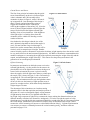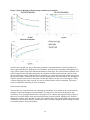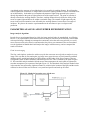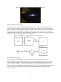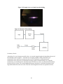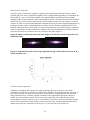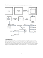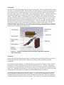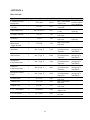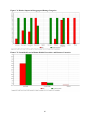
1
Designing an Optical Device for Measuring Surface Roughness
Final Report
15 December 2009
Kyle Antonini
Derek Geiger
Ryan Orizondo
Tiago Szvarca
University of Michigan
Department of Mechanical Engineering
ABSTRACT
Reliable measurement of surface roughness (Ra) is critical to quality control in a wide range of
manufacturing processes. The purpose of this project is to design a proof-of-concept device for noninvasive measurement of Ra. Through the preliminary design process for this device, we concluded that
the device must be low-cost, accurate, and safe to implement. By decomposing our device into its critical
sub-functions, we were able to generate a large pool of concept designs. With experimentation and
objective evaluation, we narrowed this pool down to an alpha design incorporating a vertical orientation,
purple LED and webcam. The final prototype was manufactured with rapid prototyping. We also made
considerations for altering this design for marketability. The prototype was completed and successfully
validated on schedule and under budget.
TABLE OF CONTENTS
EXECUTIVE SUMMARY………………………………………………………………………………..3
INTRODUCTION AND BACKGROUND….……………………...…………………………………… 4
SPECIFICATIONS……………...……………………………………………...………………………… 7
CONCEPT GENERATION………………………………………………………………………..…….. 9
EXPERIMENTATION………………………………………………………………………..................11
CONCEPT SELECTION……………………………………………………………………………….. 15
ALPHA DESIGN………………………………………………………………………………………... 17
PARAMETER ANALYSIS AND FURTHER EXPERIMENTATION...…………………………… 18
FINAL PROTOTYPE...………………………………………………………………………………… 25
FINAL DESIGN CONSIDERATIONS………………………………………………………………...30
VALIDATION TESTING AND RESULTS…………………………………………………………… 33
DESIGN CRITIQUE AND RECOMMENDATIONS……………………………………………….. .36
CONCLUSIONS………………….……………………………………………………………………... 38
ACKNOWLEDGEMENTS…………………………………………………………………………... ...38
REFERENCES……………………………………………………………………………………….......39
APPENDIX A…………………………………………………………………………………................. 41
APPENDIX B…………………………………………………………………………………................. 42
APPENDIX C…………………………………………………………………………………................. 43
APPENDIX D…………………………………………………………………………………................ .51
APPENDIX E……………………………………………………………………………………………. 52
2
EXECUTIVE SUMMARY
Reliable measurement of surface roughness (Ra) is critical to quality control in a wide range of
manufacturing processes. The purpose of this project is to design a proof-of-concept device for noninvasive measurement of Ra. This device must capture the intensity of visible light reflected by a set of
controlled surfaces and correlate this value to a measurement of Ra.
In early stages of the design process we evaluated our customer needs, benchmarked the success of
current devices against these needs, and linked them to quantifiable engineering specifications (see Table
2, page 8). With preliminary experimentation regarding the light source and relative orientation we were
able to narrow our design solutions to an alpha design (Page 17). This alpha design showed initial
promise, but was limited by the difficulty of standard image analysis. We then performed extensive
experimentation to develop a standard algorithm for image analysis and evaluate the sensitivity of our
device to changes in working distance and relative working angle (Page 18). We finalized our image
analysis procedure,and determined that the vertical orientation of our design is forgiving in terms of
working distance but sensitive to changes in working angle.
These experimental results led directly to the detailed design of our prototype device. This prototype uses
the vertical orientation and purple LED of the alpha design, but has some new features to ensure more
robust performance. The prototype has a pellicle beamsplitter rather than a cubic beamsplitter,
eliminating ghost images, and also has separate doors for the main compartment to keep the pellicle
mirror as isolated as possible. We chose to fabricate the prototype with the Dimension FDM Elite 3-D
printer. This rapid prototyping allows us to ensure the beamsplitter is set at a 45º angle relative to the
light source, and reduces machine time while simplifying assembly. The user interface was created in
LabVIEW, and the algorithms used analyzed the images based on light intensity and shape.
We also developed a validation plan to ensure that our device would meet the customer requirements
stated at the beginning of the project. We have explicit tests to determine the device’s ability to discern
Ra under different conditions (Page 33), and we also evaluated the cost and invasiveness of the device.
The completed prototype was assembled easily, with most of the parts press-fitted, save for two screws
used to fasten the beamsplitter to its frame. We ran it through our validation procedure and it met passed
all tests under normal operating conditions. The device proved to be capable of measurement with a
±2mm shift in working distance or a ±2° tilt without recalibration, and it can measure accurately from
1mm to 30mm from the surface of interest with recalibration.
We were most proud of our device’s ability to accurately and reliably make its measurements with a high
level of robustness. We were also happy that we took the objective of “test stand” a step further and made
the initial move toward a marketable design that was small and easy to assemble. We felt that we could
better improve our device if we had a lens to change our image data and zoom in upon our small area of
interest for better resolution of the light reflection pattern.
If given more time with our device, we would add an automated calibration procedure to the LabVIEW
interface that automatically thresholds light intensity into the proper output data, given images of known
Ra. This takes away any advanced calibration knowledge that the user needs to operate the device.
3
INTRODUCTION AND BACKGROUND
The University of Michigan’s Engineering Research Center for Reconfigurable Manufacturing Systems
tasked our group with designing a device that can accurately and reliably measure the roughness (Ra) of a
specific set of ground metal surfaces. This could not be completed without a thorough investigation into
the industrial applications of surface roughness measurement and the current methods of making such a
measurement.
Industry Applications
Surface roughness is a key quality indicator for manufacturing processes in a wide variety of industries.
Nano-scale characterization of surfaces is critical to understanding the electrical performance of etched
silicon films, and the dissolution behavior of pharmaceutical tablets [1, 2]. Micro-scale differences in Ra
impact the performance and lifetime of automotive engine and drive-train components, as well as the
performance of blades in turbine engines [3, 4]. Micro-characterization of surfaces is also important in
the extensive industry of protective coatings for metals [5, 6].
In the particular case of metal coating, a device capable of inline inspection of pre- and post-process
surface roughness could be a breakthrough competitive advantage. In the international shipping industry,
marine engineers use anti-fouling coatings on the surface of hulls to prevent increases in drag due to the
adhesion of fouling organisms [5]. For perspective, an increase in 5 µm of micro-roughness of a cargo
ship hull can increase the overall drag by ~4% [5]. The international shipping industry expends $380
billion in freight rates and contributes 10.12 Tg (Tg = 109 kg) of NOx and 8.48 Tg of SOx per year to the
atmosphere [5]. Given an industry of this scale, small percentage improvements in the quality of surface
coatings can have profound effects on the environmental impact and total delivered cost of goods. A
device capable of providing accurate, reliable feedback to the quality control system of an anti-fouling
coating process can have a significant, positive impact on the shipping industry and the environment.
We are working to prototype an inexpensive device capable of quickly and safely measuring the microscale Ra of surfaces of interest in a variety of manufacturing processes. If successful, the resulting proofof-concept prototype will provide breakthrough quality control feedback to any industry that is
performance-dependent on the surface roughness of materials. The next step in developing this system is
to understand the fundamental phenomena of optical surface roughness measurement.
Fundamental Technology Research
In order to understand the scientific fundamentals of the device, we explored current literature on
noncontact surface roughness measurement [7-12]. The most prevalent method in optical surface
measurement utilizes the physics of scattered light on rough surfaces. Current devices use light from a
wide spectrum of wavelengths, including infrared and ultraviolet [7]. The Beckmann-Kirchoff Scatter
Model [8], which describes the wave interaction of light with rough, opaque surfaces, was continually
referenced as one of the governing principles of this application.
From this research, we have concluded that the resolution of optical devices is dependent upon the
wavelength of the light source. Large wavelength sources can be blind to the effect of small deviations in
the surface, so we have to select an appropriate wavelength to achieve our desired resolution [9]. It is next
necessary to explore how well other current technologies make use of these scientific principles.
Benchmarking
Many surface roughness measurement devices currently exist in industry. There are three main categories
that we will analyze on a closer scale: stylus-type contact measurement instruments, non-contact laser
measurement devices, and non-contact white-light measurement devices. All three are currently used in a
4
variety of applications to analyze surface roughness—among other surface properties—of varying types
of material.
Stylus Method
Stylus-type contact measurement devices are the most
primitive type of device used to measure surface
roughness. These devices operate by moving a small probe
across the test surface to detect variations in height. This
class of devices has many disadvantages, including speed
of measurement, invasive nature, and tendency to be highly
affected by surface abnormalities. For this type of device
to accurately work, the device’s probe must remain in
contact with the sample surface. In some cases, the load
this probe exerts on the surface can cause destructive
plastic deformation. If the speed at which the stylus moves
across the surface is too high, the probe can lose contact
with the surface, distorting the output. For this reason,
accurate surface measurement with this type of device is
limited to a critical speed [13]. With this method of
operation, a small defect in the test surface can result in an
inaccurate surface roughness output.
Figure 1: Non-contact laser measurement
device setup.
Laser Scattering
Non-contact laser measurement devices are commonly
used in many industry applications. These devices operate
by emitting a concentrated laser at the test surface, either
directly or via mirrors, and using detectors to measure the
distribution of specular and diffused light reflected by the
surface [14]. This setup is illustrated in Figure 1. The
major disadvantages of this class of devices include its
limited working distance to the test surface, the potential
dangers of high energy lasers, and the laser’s inability to
examine large spans of surface. Although many laser
measurement devices overcome this last challenge by
taking multiple readings throughout a desired region, these
devices still lack the ability to take a true average reading
over a large area.
White Light Superposition
Non-contact surface measurement devices using white
light are much less common in industry. These devices
utilize the established technique of interferometry with
white light along with a CCD camera to analyze surface
Figure 2: Non-contact white-light
roughness of varying materials. This process involves
measurement device setup.
emitting white light on both the test surface and a highprecision reference surface, capturing these images with
the CCD camera and superimposing these images in order to get an accurate analysis of the surface [15].
A diagram illustrating this setup can be seen in Figure 2. One major drawback of this particular device is
the necessity of a high-precision reference surface. This can prove to be especially inconvenient when
analyzing materials over a large variety of surface finishes.
5
We decided to design a system that correlates reflected light intensity to surface roughness. To do so, it is
important to understand the possible components of our system.
System Components
The three main optical components of this system are the light source, the lens choices, and the
optoelectronic sensor.
Light Source
Visible light can be produced through several methods, like bulbs, LED’s, and lasers. It is important to
choose the right light source to meet all our needs. Each source has positive aspects and drawbacks.
A light bulb can produce the most light at the least cost. It is not a very concentrated amount of light,
though, and it will produce a lot of excess light that is of no use to us. It is also a very inefficient use of
power, and it can produce an unnecessary amount of excess heat.
An LED is a more efficient source of light, and it is available in much more concentrated arrangements,
which will better allow us to point the light at specific areas of interest. It is also widely available in
different colors, which is very important to our accuracy success, because shorter wavelength light is
capable of detecting higher resolutions on the surface of interest.
Lasers are also very attractive sources of concentrated light, but for our application, they are much too
concentrated. We want to be able to inspect over an area of 200 mm2, but lasers look at far too specific
points. Their precision also makes them prone to error if not perfectly aligned at the proper distance and
orientation.
Lens
Lenses will be essential to our device, because they will help direct the light where we want it to go. Two
important kinds of lenses that we will consider using are converging (convex) lenses and collimating
lenses. A convex lens will take incident light and concentrate it onto a smaller area. This requires more
precise adjustment, because the light through the lens gets focused at a specific distance away from the
lens. A collimating lens “straightens” out the incident light, transmitting it in a columnar fashion. This is
more versatile, because it does not require a specific focal distance for set-up, and it will keep the focus of
the image over a wider range of distances from the lens.
Optoelectronic Sensor
There are two common types of receptor devices we could use to convert light to electronic signals—
charge-coupled devices (CCD’s) and CMOS Active Pixel Sensors (APS’s).
A CCD uses a layer of silicon as a photoactive region, made up of tiny capacitors, placed upon a
transmission region. When light is incident upon the photoactive region, the capacitors are charged in
proportion to the intensity of the light upon them. A control circuit then transfers the charge from each
capacitor to the neighboring one, until reaching the end of the array, where the charge is dumped into a
charge amplifier and converting to a voltage and stored in memory.
A CMOS APS is an integrated semiconductor circuit in which each individual pixel contains a
photosensor and active amplifier. The APS’s combination of both sensing and processing into the same
integrated circuit makes for less image lag than a CCD. It will also consume less power and can generally
be fabricated more cheaply than a CCD.
Because the success of our light acquisition process is based upon light intensity detection, it is not
necessary to worry about the image quality or lag issues that distinguish the different kinds of light
6
sensors. It will be most important to obtain a sensor that can accurately distinguish slight changes in
magnitude of light intensity.
SPECIFICATIONS
Customer Requirements
In order to gain insight into how our device could improve upon current similar devices, we turned to our
customers, Dr. Hagay Bamberger and Dr. En Hong. Dr. Bamberger and Dr. Hong are researchers in the
Mechanical Engineering Department at the University of Michigan. During these meetings, Dr.
Bamberger and Dr. Hong stressed the industry’s need for a surface measurement device with the
following attributes:
•
•
•
Easily integrated to assembly line / factory setting
Accurate and resolved over a practical range of Ra values
Able to analyze larger sample region than current devices
With these specific device requirements outlined by our customers, we analyzed parts of existing designs
that we could improve upon as well as parts that did not need to be as acute for our purposes. We
separated these customer needs into well defined requirements (shown below in table 3). Each
requirement was given an importance rating of 1 to 5 which we later used in the Quality Functional
Deployment diagram (QFD – see appendix B) to rank our engineering parameters.
Table 1: Relative Importance of Customer Requirement
Customer Requirement
Capable of Discerning between Ra’s of 0.1, 0.2, 0.4, 0.8, 1.6 µm
Safe for User and Surrounding Environment
Relative
Weight
5
5
Minimized Invasiveness
5
2
Capable of Measuring a sample of area 200 mm
5
Repeatable
4
Completes Measurements Quickly
4
Easily Operable User Interface
4
Low Cost of Implementation
4
Durable
3
Easily Movable / Portable
3
Aesthetics
1
A major concern for our customer was to use this device in a factory assembly line setting. In order to
meet this request, our device needs to be quick, non-invasive, safe, easily operable, durable, and portable.
Many existing devices are bulky and use high-energy lasers that can present potential dangers in a factory
setting. Our customer is concerned with the device’s accuracy but also requires that the resolution be
catered to its specific application. We aim to build a device that can discern between Ras of 0.1, 0.2, 0.4,
0.8, and 1.6 µm. Existing devices are capable of measuring the surface roughness of a material to an
extremely high resolution but at a high cost.
7
For the specific application of inline roughness measurement, a moderate resolution is sufficient. The
final concern for our customer was to easily analyze large sample regions. Existing laser devices can only
analyze a very concentrated area. Although these devices can be set up to take multiple readings
throughout a region to produce an average reading, we aim to design a device that directly measures the
average of an entire region. In our case, the regions of interest are 1cm by 2cm test surfaces that our
customer already owns. At this point, after reaching an understanding of the customer requirements, our
team set out to assign quantifiable engineering parameters to meet these customer needs.
Engineering Parameters
We generated a list of engineering parameters that will affect this system. Using the correlation matrix in
the QFD (appendix B), we quantified how much each engineering parameter related to each customer
need. By multiplying these “correlation coefficients”—which were given a value of 1, 3, or 9—and the
importance rating of each customer need, we were able to rank the importance of each engineering
parameter for our design. Table 4 shows this ranking.
Table 2: Relative Importance of Our Engineering
Parameters
Parameter
Rank
Target
Light source dispersion
1
Optical sensor resolution
2
Distance from sample
3
Light wavelength
4
Light intensity
5
Measurement time
6
Steps in operation
8
Sensor signal-to-noise ratio
9
Weight
10
Length
11
Width
11
Height
13
Angle of incidence of light
13
As a result, we noticed that the method of
delivering light is the most important factor
to consider. Light dispersion affects the
accuracy
and repeatability of measurements.
TBD
It also affects the versatility of the sample
areas it can measure and the cost. Unlike
High
current systems that average multiple
1-10 mm
readings of small areas, we intend to disperse
the light over a larger area and take a single
380-750 nm
reading. This will reduce the complexity of
the software involved and drastically reduce
TBD
the time of measurement.
3 sec
The optical sensor is also a crucial part of our
1 step
device. The sensor resolution ranked second
in our analysis, as it was strongly correlated
10
to the resolution of our readings, the
precision of readings, and the cost. Our
1 kg
choice of optical sensor must balance
150 mm
adequate sensor resolution with low cost. As
we have mentioned before, current products
150 mm
on the market are very precise but also very
expensive. Thus, in order to create market
400 mm
share for our product, we will prioritize
reducing cost at the expense of reducing
TBD
resolution in the readings.
The distance from the light source to the sample is also a parameter of great importance. It affects the
accuracy, repeatability, and resolution of measurements. It is critical to have sufficient clearance between
the device and the sample to be feasibly implemented in a dynamic assembly line.
The wavelength and intensity of the light source are also of great importance. The wavelength will have
bearing on the accuracy and resolution of readings, as well as the safety of the device. Some
wavelengths—such as ultraviolet—can have harmful side effects. Our light source must have a
wavelength that is safe and provides adequate resolution on the surface [9].
8
The design parameters highlighted above will be the most important during the coming preliminary
design process. However, other considerations such as measurement time, geometry, weight and number
of operational steps will also be important when designing the device. These will have implications in
product implementation, product durability, safety, and user friendliness.
CONCEPT GENERATION
Functional Decomposition
After defining the critical customer requirements and engineering specifications of our device it was
pertinent to define the necessary functions that our device must perform to meet these requirements. To
accomplish this we generated a functional decomposition, and have included a visual representation of
this for our device in Figure 3 below.
Figure 3: Functional Decomposition Diagram
The primary function of our device is to receive human activation and output a measurement of Ra. Our
device is constrained to accomplish this by measuring the intensity of reflected light, so we included the
three sub-functions of: providing light to the surface (source), capturing reflected light (sensor), and
processing the captured image. It is important to note that an additional constraint on our device is that it
must be a stand-alone entity, so we have included the over-bearing function of holding the components
together. While this function may seem trivial, the orientation of the source with respect to the sensor is a
critical aspect of our design, and is intimately dependent on the way in which we fix the components.
The final item to note from the functional decomposition is a general understanding of the flow of energy
and information. While providing light, we create the by-products of heat and scattered light, the
handling of which has implications on the overall safety of the device. This functional decomposition
summarizes the essential tasks that our device must complete, and the fundamental inputs and outputs
involved with those tasks. By successfully defining the functions of our device, we can generate a
collection of concept designs to accomplish each individual function.
Concept Generation
After decomposing our problem statement into an ordered list of necessary functions, we generated
multiple concept designs to complete those functions. To generate these designs we combined ideas from
existing literature, discussion with our customers (Dr. Hagay Bamberger and Dr. En Hong), interviews
with industry experts at Picometrix (Irl Duling and Jeff White), and independent brainstorming. From
these sources we decided that the principal differentiating characteristic of our concept designs would be
the orientation of the light source and optical sensor with respect to the surface of interest. This section
details the strengths and weaknesses of our three principal orientations. Inside each principal orientation
we developed a set of sub-variations that modify the light source, optical sensor, and measuring
technique.
9
Coaxial Source and Sensor
The first of our principal orientations has the optical
sensor located directly on the axis of reflected light.
A basic schematic and CAD assembly of this
orientation is shown in Figure 4, with a CAD mockup in Appendix D. One advantage of this design is
that it is simple, and prior knowledge exists to
suggest this orientation will be successful in
resolving the roughness of the surface [16]. Since the
sensor is directly aligned with the reflected light, this
setup will also measure the highest reflected light
intensity of any of our orientations. If the brightness
of the light source is a limiting factor, then this
orientation will be suitable for detecting even the
weakest reflections.
Figure 4: Coaxial Sensor
θ
One drawback to this design is that the size of the
unit is intimately dependent on the incident angle (θ)
used. If it turns out that a large incident angle is
beneficial to surface measurement, this design will be
relatively wide in comparison to its height. Another
concern raised by experts at Picometrix was that the deviations in light intensity due to the surface would
be very small relative to the total measured light intensity. Jeff White of Picometrix commented that this
method is analogous to “measuring the weight of the captain by measuring the weight of the ship and the
captain, and subtracting the weight of the ship”. This concern was the primary motivation in the
generation of our second principal orientation.
Figure 5: Off axis Sensor
Off-Axis Scattering
In contrast to an orientation in which the sensor receives the
reflected light directly, it is also possible for the sensor to be
placed off the axis of the light beam to measure the degree of
scatter. In this orientation, the sensor is placed vertically
above the sample, while the light source shines at a slant upon
the sample. This is shown in Figure 5, with a CAD mock-up
in Appendix D. The reflected light beam is not measured
directly. This orientation measures only the light that scatters
off-axis. In this case the intensity of light upon the sensor is
greater for a rougher surface, which theoretically should have
a higher degree of scatter.
The advantage of this orientation over a head-on sensing
approach comes in the data acquisition and analysis portion of
the system. It is easier to distinguish slightly varying amounts
of light intensity when there is less light than when there is a
lot of light. Larger amounts of light will over-saturate the image, making the distinctions between too
different intensity reflections less discernible. Analogously, it is easier to weigh the captain of a ship
alone than to try to weigh the ship plus captain and subtract the weight of the ship. It is also narrower than
the coaxial design, which makes for a much more compact setup. A drawback of this design is that it
assumes the vertical scattering will increase as a discernible function of the Ra. Vigilant experimentation
was necessary to extract a relationship between the vertical scattering and Ra, and these results are
presented on pages 13-14.
10
Vertical Beam with Pellicle Beamsplitter
In order to address the concerns of working distance and
the problems associated with a changing distance, as well
as having a compact design, an attractive set-up is a
vertical orientation. If the light is collimated, it does not
need to be focused at an exact distance from the sample.
This set-up uses a 50% transmission pellicle beam splitter
oriented at a 45 degree angle from the horizontal, such that
half the light is transmitted through to the sample and half
is reflected away. Upon reflecting off the sample and
hitting the beam splitter again, half the reflected light is
again transmitted and reflected. This reflected light, less
than 25% of the magnitude of the original light source, less
because the sample is not assumed to be a perfect
mirror,but is captured by the optical sensor, which sits off
to the side. This orientation is the most compact of our
choices. It is also the costliest. A high-performing pellicle
beam splitter is the most expensive of any of our
components by far. It is also a very delicate piece of
equipment, it cannot be touched nor have any dust particles
on it. This set-up also requires that the light source be
especially bright, because it will lose at least 75% of its
magnitude from two passes through the beam splitter.
Figure 6: Vertical with Beamsplitter
Sub-variations: Light source, sensor, and measurement technique
Within each of these orientations the type of light source and type of optical sensor, and measurement
technique are still open to variation. Our original project assumption was that we would be correlating
reflected light intensity to a measurement of Ra, however the industry experts at Picometrix introduced the
idea of splitting the reflected light and correlating the resulting spectroscopy to a measurement of Ra. In
the case of spectroscopy we would use white light as the source, either a CCD or webcam device as the
sensor, and any of the three principal orientations. If we chose to measure light intensity, the source
could be a collimated LED of any color, a line LED of any color, or even a mercury arc lamp. Given
three possible orientations, two possible techniques, four possible source types, and two possible sensors
we have forty-eight possible permutations of concept designs.
Given the time constraints of this project we have limited our design space to the measurement of light
intensity rather than spectroscopy, and have selected three independent light sources. We designed a set
of experiments to enable objective selection of our alpha design among the three orientations, three light
sources, and two possible sensors. The following section details our experimental procedure and results.
EXPERIMENTATION
Since the quality of our device is dependent upon the performance of its components, we needed to test
the basic performance of the components at accomplishing their fundamental task: creating and detecting
differentiation in the images from different surfaces.
11
Experimental Procedure
We tested the following equipment:
Sources:
Purple LED (67-2064-ND):
This source produces 2200
millicandela (mcd) at an
operating current of 30mA.
Blue LED (475-2584-1-ND):
This source is about ten times
brighter than the purple one,
producing 20,100 mcd at an
operating current of 2A.
White line light: This source
is owned by our customer. We
do not have much information
about the specifications of this
source, but it has the
advantage of an integrated
intensity regulator.
Sensor:
Microsoft LiveCam VX3000
Webcam: 8 bit sensor with a 640
x 480 resolution and a 55°
viewing angle.
As mentioned previously, our design ideas also
incorporated a CCD device. We hoped to test the CCD
before this design review, but there were some setbacks.
We have a CCD sensor to experiment with, but we were
unable to integrate the CCD hardware with our National
Instruments Vision Assistant interface. For this reason, we
have 9 total sets of data to report (each of the 3 sources in
each of the 3 orientations). Each set is composed of 6
reflection images from 6 reference panels of known Ra
(0.05µm, 0.1 µm, 0.2 µm, 0.4 µm, 0.8 µm and 1.6 µm)
along with average intensity readings for each image.
Figure 8: Experimental Setup
Aside from the equipment described above, we used some
auxiliary components for some of the design set ups. For
the vertical design, we used an 80% transmission beam
splitter mounted to a simple clamp. For the blue LED light source, we manufactured a fixture made out of
Delran to couple the LED with the 7mm collimating lens. The collimating lens did not concentrate the
light as much as we had hoped, but it did produce a smaller beam than just the LED alone (size dependent
on distance from source). For the purple LED, however, additional collimation was not necessary because
the light was already directed and concentrated.
As we assembled each experimental orientation, we were careful to maintain a consistent operating
environment for each trial. However, the stands and clamps that we utilized were not designed to record
exact angles or distances. Thus, our positioning was somewhat approximate, though completely adequate
for this stage of the design process. For each data set, we placed the components in fixtures and oriented
the camera so that it delivered a quality image to the computer. Then, we simply captured an image for
each standard roughness patch. Finally, we manually selected an area of interest in the Vision Assistant
and received an average intensity reading. This average intensity was calculated from a color image, so
Vision Assistant reported the results as separate intensities of red, green and blue light. In order to convert
these three values into one grayscale value, we conducted some research and found the following industry
utilized method for doing this type of conversion [17]:
12
𝐼𝐼 = 0.299𝑅𝑅 + 0.587𝐺𝐺 + 0.114𝐵𝐵
[Eq. 1]
Where I is the grayscale intensity, R is the red intensity, G is the green intensity and B is the blue
intensity. Going forward, we will utilize methods already embedded in Matlab and LabVIEW to convert
the image into a grayscale image.
Experimental Results
There are two important aspects derived directly from this experimentation. There are the qualitative
visual cues that we got from reviewing at the pictures and the quantitative intensity data using computer
software. Figure 7 shows an example of a set of images from the vertical orientation using the purple
LED. The round reflections at the top of the images are direct reflections of the source, and the lines of
light directly below it are reflected off the test surface. As expected, increasing roughness yields
decreasing intensity of the reflection, because the light rays scatter away from the direct path of the beam.
Figure 8: A sample set of images from our data for the vertical set up. As expected, the light
intensity decreases with increasing surface roughness.
Ra = 0.05µm
0.1 µm
0.2 µm
0.4 µm
0.8 µm
1.6 µm
After processing these images, we found the numerical grayscale intensity values using Equation 1.
Experimental Conclusions
The calculated results can be seen in Figure 8. The regression lines shown were added primarily as a
visual aid to indicate a trend rather than denote a strict mathematical relation. The data on the following
page illustrates some interesting relationships. As we hypothesized, the reflection intensity decreases with
increasing roughness for the on-axis and the vertical orientations. For the off-axis, the sensor is placed to
capture scatter so the intensity increases with increasing roughness.
The first feature of these relationships that would indicate a good design is the large difference between
output intensity values. This creates differentiation that will help when our software assigns an unknown
roughness to calibrated intensity values.
Secondly, it is imperative that the curve be monotonic. This is important because the device will need to
reverse this curve to calculate an Ra from an intensity. If the curve is not monotonic in Ra, then it will not
be a function of intensity. This could result in multiple corresponding Ra values for one intensity reading.
13
Figure 9: Plots of Brightness Measurements at different orientations
From the above graphs, one can see that from preliminary experimentation the vertical orientation fits
those requirements the best. With the on-axis orientation, the webcam was saturating with brightness too
easily, which resulted in too little differentiation between each image. We realize that the saturation was a
result of experimental setup rather than failure in orientation. Further experimentation is discuss in the
Specific Challenges section. With the off-axis orientation, we consistently measured a higher intensity for
the smoothest surface followed by the lowest intensity reading on the second smoothest. We attempted to
eliminate possible causes such as reflections from the table surface, but this was a recurring issue. There
is thus an outlying point at the lowest Ra for each set of data from the off-axis orientation. This outlier
was not considered in the fitting of curves to the data.
Experimental Challenges
The procedure for experimentation was a challenge to standardize. It is best that all device and software
settings be consistent throughout experimentation. The webcam we used was not designed for such
consistency. It was preprogrammed with a wide range of color, contrast, and exposure features. Many of
these were set to auto-adjust, which posed a problem when we dealt with low lighting levels. When we
attempted to measure small amounts of scatter off a smooth surface, the exposure of the camera increased
automatically, skewing our intensity measurement results. We had to change the default settings to obtain
a consistent exposure, color, and contrast.
14
Figure 10: Possible areas of
interest
Another aspect that needs to be standardized is the selection of a
specific area of interest from the camera image. The viewing angle
of the camera encompasses more area than just the light, and for
measuring intensity, we want our software to analyze only the
portion of the area that includes that light. It is imperative to our
success that the image processing algorithm select an optimal area to
analyze, since this can drastically alter results. Figure 10 shows an
example of an image with some examples of different areas that a
user may choose to analyze. In our approach, we thought it was
better to select an area that encompasses as much range as possible
without getting any of the dark parts. Including a very dark section
could potentially yield misleading results, since the amount would be
inconsistent for each image.
One challenge that manifested itself primarily in the on-axis design
was the saturation of brightness readings on the webcam. This
webcam is capable of 256 bit configurations that carry intensity data (8 bits that be either a 0 or a 1).
Unfortunately, it was not difficult to make the camera read ‘completely bright’ and it happened for many
of our experiments, even though we were running the white light and the LEDs on minimum intensity.
Because of this, we had to minimize the amount of light we were throwing at the surface, which included
shielding ambient light. If we can eliminate this problem by using a different source such as the CCD or a
different setting, the on-axis design may seem more attractive and ambient light may not be such an issue.
However, with our current setup webcam, this is an issue we must keep at the top of our minds.
Finally, it will be a challenge to create the software that will automate the image analysis process, since
we are still working on gathering the expertise to do so. This software must have a simple user interface
that displays the roughness when the user simply clicks an icon.
CONCEPT SELECTION
After generating an extensive pool of concepts and acquiring experimental data on a more selective
group, we developed an objective method of evaluation. This section outlines the method used to
effectively assess and score each concept or component of our device. It also provides a brief look at
some of the reasoning behind our rankings from the evaluation matrix.
Evaluation Matrix
Our method of evaluation needed to take into account the experimental results and assess other important
aspects of the concepts not tested during experimentation. In addition, the evaluation method needed to
assess each concept or component fulfilling each sub-function of our device. We developed an
evaluation matrix that accomplishes everything mentioned above and assigns a discrete score to each of
the possible choices for each sub function. These scores incorporate all of the customer requirements
previously outlined in this report, as well as each requirement’s relative importance. In order to
accomplish this in an organized and efficient manner, we performed research on current methods of
engineering design evaluation. We chose to adopt a Borda count election method [18]. In this method,
voters rank potential choices, or concepts, for each design criteria, or customer requirement, and the
Borda count determines the optimal choice by taking into account the ranks and each relative requirement
importance. The completed evaluation matrix can be seen in Table 3 below.
15
Table 3: Evaluation matrix utilizing Borda count election method used during concept selection.
Customer Needs
Safe for User and
Environment
Minimized
Invasiveness
Capable of Discerning
between Specified
Ra’s
Capable of Measuring
a sample of area 200
mm2
Easily Operable User
Interface
Low Cost of
Implementation
Repeatable
Completes
Measurements
Quickly
Durable
Easily Movable /
Portable
Aesthetics
Importance
Principal Orientations
Light Sources
Vertical Off-Axis On-Axis White Line Light Purple LED Blue LED
5
2
1
3
2
3
1
5
3
2
1
0
0
0
5
3
2
1
1
3
2
5
3
2
1
1
3
2
4
0
0
0
0
0
0
4
1
3
2
1
3
2
4
2
1
3
3
1
2
4
0
0
0
0
0
0
3
1
3
2
3
1
2
3
3
2
1
1
2
3
1
Total
3
2
1
0
0
0
82
68
60
48
70
56
Evaluation Matrix Justification
The results from our evaluation matrix can be seen in Table 3 above. In the section below, we will
discuss in detail some of the thought and reasoning behind the more important rankings.
The rankings for the capability of discerning between specified Ra’s were based almost completely off of
our experimental results. As discussed earlier in the Experimental Conclusions section, the vertical
orientation seemed to eliminate the problem of brightness saturation and the irregular light intensity at a
low Ra associated with the other two orientations. In most cases, the purple LED seemed to produce
larger differences in light intensity for varying Ra’s. From these reasons, we ranked our vertical
orientation and purple LED light source highest pertaining to the capability of discerning between
specified Ra’s.
Although the safety of our device might not seem like an obvious issue, there are some potential dangers
and we took these issues very seriously. The major safety concern for a potential user of our device, or
any person in the immediate vicinity, is the high intensity light created by the light source. Even during
experimentation, it was evident that our potential light sources created light intensity large enough to be
hazardous to the human eye. In our vertical and off-axis orientations, a large portion of the light produced
is reflected to areas within the device other than the sensor location. In order to prevent this light from
interfering with the targeted light being measured, a potential solution was to allow the light to exit our
device through some sort of window or opening. In this case, this light could be a potential hazard to the
user of the device. In our on-axis orientation, the majority of the light is reflected toward the sensor and
there is no need to allow the light to exit our device. From this reasoning, we concluded that the safest
orientation would be that of the on-axis. Also, the 2A operating current of the blue LED is a safety
concern.
16
Another major criterion for our device is a low cost of implementation. The vertical orientation setup
utilizes a beamsplitter, or pellicle mirror, to split the beam of light in to two directions. This component
tends to be very expensive ($150) and would increase the cost of our overall device. The other two
orientations do not use this component. In the on-axis orientation, the sensor needs to be positioned to be
on-axis with the path of reflected light off of the sample surface. In the off-axis orientation, the sensor is
positioned vertically above the sample surface, not nearly as far from the light source. For this reason, we
predict that the housing for our device would need to be slightly larger for the on-axis orientation than
that of the off-axis (by a couple of centimeters). A larger housing would require more material and result
in a slightly larger cost. For these reasons, we ranked our off-axis orientation the highest and our vertical
orientation the lowest with respect to the cost of implementation criterion.
ALPHA DESIGN
As can be seen in our evaluation matrix in Table 3, there is an optimal choice for both principal
orientation and light source determined by the greatest total score. Our alpha design incorporates these
optimal selections into a complete device design. As previously mentioned in this report, we were unable
to experiment with our alternative sensor option, a CCD. We do plan to experiment with this option in
the future, but for now, our sensor selection will be a standard webcam. This selection is subject to
change pending further experimental results. In the remainder of this section, we will further detail our
alpha design and briefly discuss some of our major concerns with it.
Figure 11: Alpha Design CAD Drawing
CAD Drawing
A computer aided design (CAD) drawing of our
proposed alpha design incorporating the webcam,
purple LED and vertical light-sensor orientation was
created using SolidWorks 2009 (Refer to Appendix
C for more detailed drawings and dimensions). A
screenshot of this image can be seen in Figure 9.
Although the optimal selections for device
components have been tentatively made, the specific
model types within these broader categories is not yet
know. For instance, although we may have chosen a
webcam as our current sensor, the specific webcam
model type is unknown. For this reason, the labeled
images representing the components are simple,
rough drawings with sizes that we feel are accurately
comparable to potential model types. The
positioning of the elements shown in the CAD
drawing is also consistent with our experimental
setup. For this reason, we strongly believe that the
setup shown in Figure 9 is realistic and fully feasible.
As seen in the figure, the overall height of the model
is just over 7 cm, and the dimensions for the rest of
the model can be understood relative to this.
Our primary concern is the tradeoff between cost and size of our alpha design. The alpha design has the
smallest overall size, but also results in the greatest overall cost of implementation, due to its use of a
beamsplitter. This component can cost in the range of $200 - $1,000. The minimized size of the alpha
design positively correlates with many of the important design criteria such as easy mobility and
operability. This tradeoff is a very important issue and one that we will need to further discuss with our
customer in order to gain better insight.
17
A predicted positive outcome of our alpha design is its versatility in working distance. By utilizing the
vertical light-sensor orientation, we suspect that a variation in working distance will have a minimal effect
on its functionality. In the other two orientations the amount of light being captured by the sensor is
directly dependent on the point of light reflection off of the sample surface. The point of reflection is
directly related to the working distance. Therefore, working distance directly affects the ability of the
sensor to capture light and discern Ra within a reasonable range. The amount of light captured by the
sensor in the vertical orientation is not affected by the working distance, because there is no angle of
incidence. We plan to do extensive experimentation in the near future to prove or disprove this
prediction.
PARAMETER ANALYSIS AND FURTHER EXPERIMENTATION
Image Analysis Algorithm
In order for our experimental data to be viable, the image analysis had to be standardized. As of Design
Review 2, our experimental results had been based on analysis of arbitrary areas manually selected from
each acquired image. Although we attempted to consistently select the same area each time, we could
never trust our results to be entirely consistent unless the process was automated. Thus we formulated
several algorithms in Matlab that would analyze the images in different ways, and we compared the
results of each one.
Fixed Area Averaging
The first—and simplest—method we tried was to pick the exact same area of pixels to analyze in every
image. This was done by first turning the .jpg image into a grayscale array of pixel intensities and then
defining specific starting and ending rows and columns as the border of our area of interest. Then we
averaged the values of all the intensities within that specific area. This is outlined by the chart in Figure
12. We tested this analysis method with both an area that encompasses the entire patch of light and an
area that encompasses just a portion of the light (Figure 13). The drawback of this analysis method is that
it does not take into account any slight movements or variation in the location of the light, and the results
will thus be skewed if the area of interest is very small and specific and ends up off center.
Figure 12: Method of averaging over a fixed area
18
Figure 13: Sampled areas of interest chosen to test algorithm
Area Selection Based on Centroid
In order to negate the effects of a possibly shifting light patch, we wanted an algorithm whose area
selection was always based on the exact location of the light. This led us to devise a formula that would
find the “centroid” of the light intensity, which we assumed would be at the physical center of the light in
the image. The formula output the coordinates of this specific point within the image array, and then a
constant rectangular area would be defined around that central point. The intensity values within this new
constant area were then averaged. This is outlined in Figure 14.
Figure 14: Method of averaging in an area around a centroid
Thresholding and Averaging
Another form of area selection that was considered was based on a threshold argument. It was
hypothesized that the amount of pixels above a specific intensity would follow some sort of trend as the
surface roughness changed. This algorithm took an image array and disregarded all pixels whose value
was below a certain amount, e.g. 82. We would end up with an area of somewhat irregular size as in
Figure 15. We then averaged these remaining pixel intensity values. We tested this algorithm at threshold
values of 82 (the maximum intensity of light from the roughest sample) and 130. This algorithm is
outlined in Figure 16.
19
Figure 15: Example of an area found from thresholding
Figure 16: Method of Thresholding
Preliminary Results
After taking five sets of images at each Ra value, we ran each image through each algorithm and received
the following results in Figure 17. The fixed area averaging yielded too much inconsistency per
measurement with a small area, as shown by the error bars, and almost no differentiation per
measurement with a larger area. The threshold averaging yielded a smooth looking curve with little
inconsistency per measurement for a threshold value of 82. However, there was not much differentiation
between successive points. The centroid method followed a smooth curve, had little inconsistency and
large differentiation between each value. Thus the centroid argument became our algorithm of choice.
20
Figure 17: Experimental results for 5 data sets analyzed with different algorithms.
21
Shape Sensitive Algorithm
In all our results, averaging was incapable of properly discerning the two smoothest surfaces, whose
reflected light areas were of comparable brightness. This required another algorithm to be formulated. We
noticed that for every set of data, the brightest, most saturated light in each image followed a shapechanging trend from the smoothest to the second smoothest surfaces. The light reflected off the smoothest
surface was very circular, and the light from the second smoothest surface was more elliptical, as shown
in Figure 18. Thus we created an algorithm that compared the aspect ratio of the brightest light portions of
the images. In other words, we thresholded the area above values of 240 and compared the ratio of the
height to width of the areas in each image. As expected, the smoothest area yielded a height to width ratio
closer to 1 than did the second smoothest area, and there was a large enough difference between the two
values to account for any variation in area size as shown in the plot in Figure 19.
Figure 18: Images from 0.05 µm (left) and 0.1 µm (right). Note the more circular saturated area in
the 0.05 µm image
Figure 19: Experimental results for the shape algorithm showing a distinct difference between Ra’s
of 0.05 µm and 0.1 µm.
Final Measurement Algorithm
Ultimately, the method used to analyze the images and output the most accurate Ra values used a
combination of all the above methods. As outlined in the flowchart, the algorithm turns the raw image to
grey scale and makes it an array of intensity values. It then looks at a large predefined area within the
image. Within that area, it finds the centroid coordinates of the light and from that point it defines a
smaller area centered at the centroid. The intensity values within this area are then averaged. If the
average intensity is below a specific value, it is correlated to a specific Ra, chosen by bins defined by the
errors from our experiments. If the intensity is above a specific value, the shape algorithm takes effect,
and the aspect ratios are correlated to an Ra of 0.05 or 0.1. See the flow chart in Figure 20.
22
Figure 20: Final measurement algorithm, combining multiple methods of analysis
Vertical Misalignment
Earlier, we had hypothesized that our vertical design would be less susceptible to changes in working
distance. We performed further experimentation to validate this claim. We excluded the off-axis design
due to the outliers in the data that we were unable to remove. Thus, we tested both the on-axis and the
vertical design for changes in working distance from 0 mm to 8 mm. All images were taken at a standard
roughness of 0.2 Ra and analyzed using the ‘centroid’ scheme. Figure 21 shows the results from this test.
23
Figure 21 indicates that the vertical design is indeed more capable of attaining consistent readings for
different working distances. There were smaller percent shifts in vertical readings than that of on-axis
readings. Also, on the on-axis setup, we placed the light source and camera such that they would be
aligned halfway through our test (~3.5 mm height). The readings were somewhat consistent before this
point and after this point. However, there was a big shift between 3 mm and 4 mm. This is due to the
sudden misalignment of the source with respect to the sensor. Since this design operates with the source
and sensor aligned, this data would indicate that a vertical shift of the surface of only 0.5 mm would have
a significant effect on our reading. For this reason, we concluded that small changes in working distance
would indeed be a concern with the on-axis design.
Figure 21: Results for vertical displacement tests for the on-axis and vertical orientations at 0.2 Ra.
Angular Misalignment
Another important type of surface variation is angular misalignment. We considered two different angles
that could be misaligned, and we called them the “long” angle and the “short” angle after the length of the
pad that we were rotating. Figure 22 illustrates which rotation is referred by what name.
We ran the centroid algorithm on each Ra value and the shape algorithm for 0.05 and 0.1 Ra for long and
short rotations between 0° and 4°. The results can be seen in Figure 23.
Figure 22: Angular misalignment
experimental setup showing long
and short axis rotation.
LONG
SHORT
24
Figure 23: Results for variation of surface angle experiments.
The plots above show that our centroid algorithm is rather sensitive to angular changes. Since this is
currently the base algorithm for our device, this is something we must address. The good news is that the
overall trend still holds at different angles. This means that our device can be recalibrated to work at
different angles. However, if the device has been calibrated to measure at a certain angle and then that
angle changes, this data indicates that the readings would no longer be accurate. Moreover, the shape
algorithm was surprisingly robust. From the plots above one can see that it would have predicted the
proper Ra even without recalibration.
We will attack the issue of the centroid algorithm from two angles. One, we will continue working to
make our software less susceptible to shifts in the surface. We will also look into ways of implementing
easy calibration procedures and add them if time allows. The other angle of attack is the hardware. We
will make a test stand as described in the “Components” section below to ensure that the angle of the
device stays constant.
FINAL PROTOTYPE
This section will introduce and give an in-depth description of our final prototype design. It will also
provide a description of the components housed inside the device and an assembly and fabrication plan
for the prototype.
25
Description
Our final prototype is made of Acrylonitrile butadiene styrene (ABS) and is approximately 91 mm x 85
mm x 74 mm. It is comprised of three compartments: the main compartment, the top compartment and
the side compartment. A computer equipped with our LabVIEW interface must be connected to the web
cam housed inside our device during use. Our prototype is fully functional in that it has all of the major
capabilities that our final product would have. More
specifically, our final prototype has the ability to be
positioned over a test surface, capture an image, analyze
that image and output a determined Ra value. Figure 24
shows the device both with and without its doors. Note
that the computer that the device would be connected to
during use is not shown in this figure. Please refer to
Appendix F for more detailed drawings. It is also
important to note that as part of our final prototype, we
will also have a stand on which to mount our device.
This stand will hold the device so that the vertical axis of
the device is normal to the test surface and will be
discussed in further detail in the Components subsection
of this section. This stand is not pictured in Figure 24.
Modifications from Alpha Design
While performing further experimentation and
consulting with our customer, we decided to make some
modifications from our previously mentioned Alpha
Design.
The most critical modification to our final prototype
design from our Alpha design is centered around the
doors to the three compartments of our device. There
were two doors on the Alpha design that both operated
on hinges. The final prototype has three separate doors
that all operate on tracks integrated to the main body
Figure 24: A CAD model of our final
device. This change allows the user to open the side and
prototype both with and without doors.
top compartments without exposing the main
compartment to the ambient environment. This is important because the main compartment houses the
pellicle mirror which is extremely sensitive to dust and other ambient elements. These doors were
designed so that the friction along the track surfaces suffices to keep them closed during use.
Another modification is that we have eliminated the tapered column leading to the window previously
found on the Alpha design. As you can see from Figure 24, the bottom of our device is now flat. This
modification essentially brought the potential test surface closer to the pellicle mirror located directly
above the window. This modification increases the size of the light reflection in the image as well as
makes the device more compact. Our final prototype also uses a 9-volt battery to power the LED. The
Alpha design had assumed the LED would use an external power source. This modification allows the
device to be more portable. We’ve also added a transparent protective window to the viewing window on
the bottom surface of our device. This window is planned to be made from Plexiglas and will prevent
dust and other debris from collecting on the sensitive pellicle mirror. The final prototype also has a
removable pellicle holder. This modification allows the pellicle mirror to be easily moved in and out of
the device if maintenance or replacement is necessary.
26
Components
The main body of the final prototype houses eight main components. The top compartment houses the 9volt battery, circuit board and LED. The LED used in our final prototype is a Luminex 5mm purple LED.
In the sidewall of the top compartment, there is a simple push on/off switch that will operate the LED.
The switch used in our device is a Mini SPDT 3-Amp Push On/Push Off Switch. The main compartment,
found directly beneath the top compartment, houses the pellicle holder, pellicle mirror and protective
window. The pellicle holder is a manufactured piece made of ABS, the same material as the main body.
The pellicle holder and pellicle mirror are attached to each other with two standard 2-56 screws. When
placed in the main body, the pellicle holder holds the pellicle mirror at a 45 ˚ angle with the horizontal.
The pellicle mirror used in our device is an Edmund Optics 1” Diameter 50R/50T Pellicle Beamsplitter.
The protective window is also a manufactured component that is made out of Plexiglas. The side
compartment houses only the web cam. The specific web cam used in our final prototype is a Microsoft
LifeCam VX-5000. Figure 25 below shows a model of the final prototype with the main body shown as
transparent so the components are clearly visible.
Figure 25: A model of the final prototype showing the eight main components
housed in the device.
Fabrication
After we developed our final prototype design, we generated three possible plans to fabricate our device.
The three potential fabrication plans were subtractive machining, additive machining and rapid
prototyping.
In the subtractive machining plan, we would essentially start out with one solid piece of stock material
and subtract, or machine, out blocks of material to form the various cavities. The three compartments
described earlier would be machined out most likely using a mill and the various holes would be created
using a drill. Although this plan produces a very robust, single-piece main body, the cavities for the three
compartments in our design are quite complex and would making milling very difficult.
In the additive machining plan, the main body of the device would be manufactured in pieces and then
assembled together with mechanical fixtures or adhesive. The main and top compartments would be
manufactured by removing material from a block of stock material using a mill. The side compartment
would be manufactured separately in the same manner. These two pieces would then been joined using
27
mechanical fixtures. This plan again requires difficult
milling operations to create the cavities for the compartments
as well as adds additional fixture components to the device.
In the rapid prototyping plan, we would utilize a unique
three-dimensional printing service available to us at the
University of Michigan to have the entire body of the device
made in a single piece of material. The three-dimensional
printing service uses a machine called the Dimension FDM
Elite to create a layered composite object from a CAD file.
The Dimension FDM Elite is capable of producing extremely
complex geometries with tolerances as small as 178 µm. In
Figure 26: Pellicle assembly showing
this plan, we would generate a precise CAD model of our
labeled components.
prototype and import this file into the Dimension FDM Elite
in .STL format. The turnaround time for an object of our
size and complexity would be approximately 40 hours. Minor post-process machining such as sanding
would then be done to the completed body.
The most important factor in our final choice of a fabrication technique was the accuracy of our
manufactured components. The success of our design heavily relies on the precision of the angle at which
the pellicle mirror is held. As mentioned earlier, the milling operations required to machine out the
cavities for the compartments is quite complex and we did not feel that we would be able to accomplish
the accuracy necessary. For this reason, we chose the rapid prototyping technique to manufacture our
prototype. The main body, the doors and the pellicle holder will all be manufactured using this method.
All of the parts made with this method will be made out of ABS, a rigid, lightweight thermoplastic.
As mentioned earlier, this fabrication method builds the parts through an intricate layering process. For
this reason, the final parts do have varying directional strength. The material is fairly resistant to forces
applied normal to the layering, but could be less resistive when a load is applied parallel to layering.
Because our device has no “expected” loads, we do not foresee this being a major problem. This
technique allowed us to greatly decrease our estimated manufacturing and assembly time. The total cost
of this type of manufacturing, including material, labor and machining costs, will be $170.
Assembly
The assembly of our device is quite simple. As previously mentioned the main body of our device will be
manufactured as a single piece and requires no assembly in itself.
The first step will be to attach the pellicle mirror to the manufactured pellicle holder. The pellicle mirror
has a hard plastic ring around the mirror that has two tapped holes. The pellicle holder was designed to
be manufactured with two through holes positioned to match up with the tapped holes on the mirror. Two
standard 2-56 screws will be used to attach these two components. Figure 27 shows a schematic drawing
of this assembly.
Next, the circuit board, protective window and on/off switch will be attached to the main body in their
respective locations using standard epoxy. It is important to note that the circuit board, consisting of
simple wiring and resistors, will be assembled outside of the main body and then epoxied in. The main
body has been designed so that the 9-volt battery, purple LED, web cam and pellicle unit (the attached
pellicle mirror and holder) can all be press–fitted in to their respective locations. Lastly, the three doors
slide in to the main body on integrated tracks. Figure 27 shows the main body after fabrication before
assembly and the fully assembled main body.
28
Figure 27: Prototype before and after assembly.
User Interface
The user interface that a potential user would encounter on the computer connected to our prototype was
created using LabVIEW. Figure 28 shows a screenshot of the user interface. For our prototype’s most
basic feature, a potential user only needs to perform three steps. First, the user needs to physically
position the device directly above the surface being measured. This can be done by either moving the
surface while keeping the device stationary or vice versa depending on the nature of use. After the
prototype is positioned correctly, the user uses the “Snap Picture” button on the interface VI to capture an
image. In order to ensure that the user captures an image of the desired surface region, there is a “Live
Image” window featured on the VI to allow the user to see the potential image to be captured. Lastly, the
user uses the “Analyze Image” button on the VI to command the interface to process the image and output
a determined Ra value. The VI also offers more complex features that allow the user to alter camera
settings, threshold limits and geometric area selection parameters. These options are strictly for
calibration purposes and are not needed during standard use.
29
Figure 28: A screenshot of the LabVIEW user interface encountered during use of the prototype.
FINAL DESIGN CONSIDERATIONS
This section will outline major differences between our final prototype design and the final, marketable
design of our device. These differences arise primarily due to the major differences in expenses and ease
of manufacturing between producing a single functioning prototype and mass-producing a marketable
product.
Material Selection and Fabrication
For our one of a kind prototype it was rather clear that rapid prototyping was the optimum method of
fabrication. With the resources available to us here at the University, we only had two options: a brittle
plaster powder ($0.20 per cc) or ABS plastic ($0.40 per cc). We chose the latter for its strength and
machining capabilities.
However, when designing a final product intended for market, we had to look much more carefully at
potential materials and fabrication methods. The tool that we utilized to do this is CES EduPack 2009.
This software is essentially a huge database of materials and manufacturing processes. The user can
specify limits for various properties and the software will keep track of the materials that meet the criteria,
as well as will show what processes may be performed to the materials. Table 4 shows the limits that we
used for our design.
30
Table 4: CES Parameters for the final design.
Parameter
Minimum Maximum
Price
0
1.3
Max Service Temperature
120
Min Service Temperature
50
Electrical Resistivity
Transparency
Water Resistivity
CO2 Footprint of Production
Recyclable
1 x 10⁶
Opaque
Excellent
0
4
Yes
Unit
$/lb
°F
°F
µohm.cm
lb/lb
From the table one can see that we are concerned with price, durability, optical properties and
environmental effects. We want a device that will cost at most a few dollars of material. Also, it must
operate in temperatures that will be expected in a typical manufacturing line, so the maximum should be
above 120°F and the minimum should be below 50°F. The material should be able to resist water and it
should not conduct any electricity from the circuitry in the top compartment. Moreover, we tried to
minimize adverse effects on the environment by limiting the carbon footprint of production to a rather
low value (4 lb/lb) and by making our product out of a recyclable material. The list of materials that fit
these criteria is shown in Figure 29, ranked by price.
Figure 29: All materials fitting our selection criteria
31
Figure 30: Manufacturing processes for
high impact polystyrene.
From Figure 29 one can see that the cheapest material that fit our criteria was HIPS, or high impact
polystyrene. This is a low density (0.038 lb/in3) polymer with impact modifiers for greater impact
resistance. This material allows our device to be light, cheap, durable and environmentally friendly. In
fact, with this material our device would weigh 0.4 lbs (with no components) and would cost $0.28 of
material. This material is often used to make toys and household appliances, and it does not deform very
easily (E = 3 x 10⁵ psi).We feel that this would be the best material to use for the main block and all the
doors – every part that is not directly bought as a component. Please refer to Appendix E for more
information about this material.
Another great feature of the CES software is that it suggests manufacturing processes that are compatible
with materials in its database. The CES process suggestions for HIPS can be seen in Figure 30. Most of
the processes shown would not be suitable for our device. All common machining processes (such as
milling, turning, drilling, etc) would not be adequate for making our device. These processes would not be
able to make such intricate detail on such a small scale while keeping tight tolerances. Thus, we
eliminated these processes from our palate. Also, most methods of molding would also not work with our
device as it is currently designed. Processes such as blow molding, polymer extrusion, rotational molding,
or polymer forging are not able to create very detailed shapes with multiple compartments. We were left
with thermoplastic injection molding and rapid prototyping.
The decision between these fabrication methods then comes down to the market size and the amount of
fabrication we intend to undertake. Injection molding has very high initial tooling costs (from $3,000 to
$90,000 for a mold) but can produce many units very quickly (60 to 3000 per hour) for low additional
cost. Rapid prototyping, on the other hand, has low tooling costs ($40 - $90) but these costs are recurrent
for every unit. Also, the production rate is only 0.02 – 0.5 units per hour. Thus, for small production sizes,
we would rapid prototype our device in polystyrene. However, if we were to sell about 10,000 units or
more we would use thermoplastic injection molding for fabrication.
Components
Another major difference between our prototype and the final product is in the individual components
inside the device. Some of our components are marketed products designed to be stand-alone devices
with unnecessary casing and features. In a mass-production scenario, these parts would be replaced with
“bare” components bought in bulk straight from the manufacturer. These modifications would most
likely make our complete device cheaper and more compact. These changes, along with some others, are
discussed in greater detail below.
As previously mentioned, the sensor used in our device is a Microsoft LifeCam VX-5000. This product is
marketed as a web cam mostly intended for users looking for a method of live communication over the
Internet. The web cam consists of the camera itself as well as a USB compatible cable to connect to a
computer. As one would expect, the camera comes with a protective and aesthetically pleasing casing
and loads of user options to alter camera settings. Due to its nature of use, the web cam is also designed
to have a very wide viewing angle. These detailed camera-setting options, extraneous casing and wide
viewing angle are not at all ideal for our intended use of a sensor. Our ideal sensor would be small, have
very basic, if any, camera-setting options, and have a much narrower viewing angle. We foresee the
sensor component used in the final product as still having a USB compatible connection to connect to a
computer. In order to decrease the viewing angle and also add greater resolution to our sensor, we would
mostly likely utilize a lens in conjunction with our sensor. For the resources available to us and the nature
of our single prototype, these modifications are not practical. However, in a final product, these changes
would increase the quality of our device, decrease the overall cost of our device, and allow our device to
be more compact.
32
Our final prototype uses a standard 9-volt battery to power the LED housed in the top compartment. We
chose this component because it best suited our needs and intended purpose for the prototype. The power
used for the final product is very dependent on its intended use. The requirements of the power source are
very simple and could be met by a multitude of different options. If the final product were meant to be
permanently mounted on an assembly line in a factory setting, utilizing an external power source might be
the most practical option. If the device is intended to be constantly moved to be used in various locations,
a battery powered setup similar to that of our prototype would most likely suffice. As one can see, there
are many options for the power source and we feel that our design could be easily catered to meet the
needs of almost any specific use.
As previously discussed, our device’s accuracy is sensitive to the angle of the test surface relative to the
vertical axis of our device. Our device is capable of functioning at angles deviating from the vertical axis
being normal to the test surface, but a recalibration procedure would need to be performed. We have
integrated features in to our user interface to allow the user the options necessary to manually recalibrate
the system, but in a marketable product, this issue would be addressed to a much greater degree. Not only
would we include more calibration-related options in the user interface, much of the process would be
automated. We would also most likely develop a user manual solely dedicated to recalibrating the device.
VALIDATION TESTING AND RESULTS
In order to complete the design process, we must validate that we have in fact met all of the customer
requirements outline on Page 7 of this report. We have stayed within our budget of $400 (see Appendix A
for a detailed breakdown of the costs) and our device does not touch the surface that it is measuring
(15mm standoff). Table 5 shows other engineering parameters, the target values we had established and
the final results.
Table 5: Results of engineering parameters.
Rank
1
2
3
4
5
6
7
8
Parameter
Optical Sensor Resolution
Standoff
Light Wavelength
Light Intensity
Measurement Time
Steps in Operation
Weight
Size
Target
8-bit
1 - 10 mm
380-750 nm
< 5000 mcd
< 3 sec
1 step
< 1 kg
< 150x150x400 mm
Result
8-bit
1 - 30 mm
480 nm
< 2000 mcd
< 1 sec
1 step
< 1 kg
85x75x90 mm
The table shows that we met or exceeded all of our targets for the engineering parameters. In order to
validate the accuracy and repeatability of the device, we performed detailed validation experiments that
are outlined in the following section.
Reliability Validation
Each trial, or each measurement, of our device can be interpreted as a Bernoulli trial (it can either succeed
and output the proper Ra, or fail and output the wrong Ra). Since each trial has some probability of failing,
and this probability is not affected by other trials, we felt that the best statistical test for reliability of our
device would be a Binomial Test. For each of the configurations below, we utilized a 95% confidence
interval to find the bounds for the probability of proper functionality. For all tests, our device was set to
output results according to the thresholds shown in Table 6.
33
Table 6: Thresholds for the device.
Ra
0.05
0.1
0.2
0.4
0.8
1.6
Intensity (bits)
>145
>145
100 - 145
75 - 100
45 - 75
< 45
Aspect Ratio
> 0.6
< 0.6
15mm standoff, 0° angle
This was our baseline set of trials. The device is designed to operate at a 15mm distance from the surface
of interest and normal to the surface. We performed 120 trials (20 sets of 6 pictures) with this
configuration and all of the pictures output the proper results. This yields a confidence interval of 0.97 –
1.0, meaning that we expect the device to work at least 97% of the time.
We also recorded the output intensity and aspect ratio for each of the trials, so that we could get an idea
for how robust the device is. Table 7 shows the average intensities, the aspect ratios, and the errors based
on the 120 trials. The errors reported are two times the standard deviation between all the trials. The table
shows that the errors of the experiments were very small (maximum of 2.45 bits and 0.045 aspect ratio)
compared to the gap between the averages (23 bits and 0.484, respectively). This gave us much
confidence in the reliability of our device. The next step was performing similar tests with changes in
standoff and changes in angle to capture the sensitivity of our device to movement or misalignment.
Table 7: Results for baseline tests at 15mm standoff and 0° angle.
Ra
0.05
0.1
0.2
0.4
0.8
1.6
Average
Intensity
198.10
181.65
111.35
87.00
56.45
33.45
Error
2.04
2.45
1.75
2.05
1.52
1.21
Aspect
Ratio
0.882
0.399
Error
0.045
0.022
Changing standoff, 0° angle
The next experiment was to change the standoff by increments of 2mm to test the device sensitivity. This
was done using 3 spacers of 2mm each. We set up the device with the usual 15mm standoff with one
spacer already placed. Then, we added a spacer to get readings for +2mm and removed the original spacer
to get the reading for -2mm standoff.
34
Figure 31: Standoff misalignment results. The lines shown are the thresholds between the Ra values.
We performed 60 trials for +2mm and 60 trials for -2mm and the device succeeded in getting the proper
reading in all trials. This translates to a confidence interval of 0.95 – 1.0, meaning that we expect the
device to work at least 95% of the time. The results can be seen in Figure 31.
The lines that are shown are the thresholds between the Ra values, and the errors are two times the
standard deviation of the readings. The graphs show that within error all of our readings lie within the
proper thresholds. Thus, we are comfortable asserting that our device is capable of operating within 2mm
of vertical misalignment without the need for recalibration.
It is also relevant to find the bounds of standoff where the device is operational with recalibration. To
perform this test, we started at 1mm of standoff (just barely above the surface) and took 3 sets of 6
readings. We noted that the results were such that a calibration routine could be written to differentiate
between the six Ra’s reliably. We repeated this process for 5mm, 10mm, 15mm, etc until the algorithm
broke down. We found that the algorithm starts to become unreliable over 30mm of standoff. The biggest
factor that contributes to this is that the useful part of the image becomes smaller as you increase the
standoff. Thus, after a certain point, the algorithm starts to catch some area outside of the light reflection
when it averages the intensity. Also, when we increased the standoff we started so see the adjacent
surfaces in our images. These can also throw off the measurement by introducing extra reflections in the
image. From this, we concluded that the device can operate between 1 and 30 mm of standoff with
recalibration.
15mm standoff, changing angle
The final validation experiment was to rotate the long axis of the surface of interest by 2° to simulate
angular misalignment. We achieved this by placing spacers on one side of the scratchpad with the proper
height to create a 2° angle (the length of the scratchpad can be measured, so this is a simple trigonometry
problem).
35
Figure 32: Angle misalignment results. The lines shown are the thresholds between the Ra values.
We performed 60 trials with the angled surface and the device succeeded in all 60. This translates to a
confidence interval of 0.95 – 1.0, meaning that we expect the device to work at least 95% of the time. The
results can be seen in Figure 32. As before, the graphs show that within error all of our readings lie within
the proper thresholds. Thus, we are comfortable asserting that our device is capable of operating 2° off of
angular alignment without the need for recalibration.
DESIGN CRITIQUE AND RECOMMENDATIONS
We are very proud of our final device and its capabilities. There are many aspects of our device that
exceeded our initial expectations and some that we would look to improve upon if given more time. The
purpose of this section is to outline these strengths and weaknesses.
Strengths
Our initial project objective was to design and build a test stand to explore using visible light to determine
surface roughness. One aspect of our work that we are very proud of are our efforts in taking the initial
steps towards making our device a marketable product. Our final device is much more than a test stand.
Its small, compact design makes the device easily portable and usable in a variety of practical settings.
Our device’s design also allows for all major components to be press-fitted into the device, eliminating
the need for fasteners with the exception of the two screws fixing the beamsplitter to its removable frame.
We feel that this feature makes the assembly process on a mass-production scale much more feasible.
Another feature of our device that we feel is very impressive is its robust functionality and build. We
expected our device’s function and accuracy to have decreased sensitivity to changes in the home position
when compared to that of laser devices, and our validation results confirmed our expectations. As can be
seen in our “Validation Testing” section, our device successfully functions with significant changes in
working distance and angle without recalibration. By creating the main body of our device from a single
piece of material, the build of our device is also very robust. Although the device is not intended to
encounter any forces beyond normal “handling” wear, we feel that this increased durability is a strong
aspect of our device.
Potential Improvements
One option that we would have explored given more time is the addition of a diffuser to the light source.
A diffuser would essentially scatter the light before reaching the test surface, allowing for a more even
distribution of light across the region of interest. Our current device utilizes a round LED with no
36
diffuser, and light distribution on the test surface is therefore a circular pattern. We feel that by adding a
diffuser and spreading the light more evenly across the surface, we would be able to simplify our
algorithms to be solely based off of light intensity (our current algorithms analyze light intensity and
shape). We also feel that this addition would reduce the chance of error in our device caused by a small
surface abnormality.
Another aspect of our device that we feel could be improved upon is the resolution of our captured image.
Our current sensor setup has a field of view much larger than is needed for our purposes and uses only a
small fraction of our sensor’s available pixels. With the addition of a lens to our sensor, we would be able
to decrease the field of view to an optimal size and drastically increase the resolution of our captured
image. Theoretically, an increase in the resolution of our captured image should allow our algorithms to
perform a more detailed analysis, and better differentiate between varying values of Ra. Extensive
experimentation would have to be done in order to determine what type of lens would produce optimal
results for our device.
Finally, our current device requires a manual calibration process each time a change in the standoff of
greater than 2mm has been made. In order to improve the user convenience of our device, we would look
to expand the functionality of our code and user interface to include an automatic calibration process.
The current manual calibration process essentially consist of capturing images of a set of known surface
roughness values, analyzing the algorithms’ resulting light intensity and shape parameters, and setting the
threshold values such that the surfaces with differing roughness can be optimally differentiated. With
more time and effort, our existing code could be expanded to automatically determine threshold values
from a set of known images.
Suggested Directions
To expand the scope of our project, we have recommendations to our sponsor for future paths to explore.
The purpose of this section is to describe these paths and the impact that they could have on our device.
Our current device is meant to be used only on ground, flat surfaces. We believe that a worthwhile
endeavor in the future is to explore the possibility of using our device on other types of surfaces. More
specifically, our device should be tested on contoured surfaces that have been manufactured in manners
other than grinding, such as milling, turning, or reaming. It is possible that our device could work on
surfaces such as these, but may need a different set of algorithms to do so. The feasibility of this option
could be determined through experimentation. In order for this device to be practical and useful in a realworld setting, its use needs to be extended beyond the realm of flat, grinded surfaces. Exploring the path
described above would be the first step in expanding the use of our device.
Another beneficial question to explore is whether our device could be used to differentiate between
smaller increments, and values in a much larger range of Ra. Our current device can differentiate between
surfaces with values of Ra of 0.05, 0.1, 0.2, 0.4, 0.8, and 1.6 µm. In order to be competitive with current
surface roughness measurement devices, we believe that the use of our device would have to be expanded
to a set of Ra values beyond its current one. It is possible that our algorithms, or maybe even the entire
methodology of using visible light, will break down at some extreme, or some small resolution of values
of Ra. Once again, this option could be explored through experimentation.
Both of these paths are steps in expanding the functionality of our device, while also making further
strides in transitioning from a proof-of-concept test stand to a practical, fully-marketable product.
37
CONCLUSIONS
Our team was charged with designing a test stand that proved low-intensity visible light was capable of
successfully differentiating between standard Ra values of ground metal surfaces. From functional
decomposition, we broke our design into the basic components of light source and sensor. Through a
series of experiments, we concluded that the best design would include an LED oriented vertically above
the surface of interest, utilizing a pellicle beamsplitter to send the reflected light to a webcam.
The product was refined through further experimentation and design into a compact, easy-to-assemble
device, taking the proof-of-concept objective closer to a marketable device. It was manufactured with
ABS plastic using rapid prototyping. A user interface was created in LabVIEW, evaluating roughness
with an algorithm that binned light intensity and shape to specific Ra values. Further validation testing
proved it to be a robust design, capable of significant variations in stand-off distance from the surface of
interest.
We thus completed our objective and took further stops toward making a marketable product. If given
more time, we would also add an automated calibration procedure to our LabVIEW VI. We would also
expand our capabilities beyond just ground surfaces, to other types of machining.
ACKNOWLEDGEMENTS
We would like to acknowledge several people for their help and support throughout this project. It could
not have been completed without their invaluable contributions: Section leader Professor Yoram Koren;
Customers Hagay Bamberger and En Hong; Expert Consultants Irl Duling, Jeff White, and Chris
Megdanoff of Picometrix; GSI Dan Johnson; Professor Reuven Katz; Administrator Julie DeFilippo; Lab
Supervisor Steve Erskine; and the other students in Professor Koren’s section of ME 450, who often
provided groundbreaking insights that furthered the success of our project.
38
REFERENCES
1. Huynh, Van-Minh and Luk, Francis M. “Method and apparatus for assessing surface roughness.” U.S.
Patent 4,878,114. 31 October 1989.
2. Seitavuopio, Paulus and Heinämäki, Jyrki and Rantanen, Jukka and Yliruusi, Jouko. “Monitoring
Tablet Surface Roughness During the Film Coating Process”. AAPS PharmSciTech 2006; 7:2, Article 31.
3. Hennies, Hans-Henning and Kessler, Gunter and Krafft, Gerd and Miller, Georg and Schumacher,
Gustav. “Protective coating for turbine blades”. U.S. Patent 6,149,389. 21 November 2001.
4. “Engine Blade Coating - Using HVOF in MCrAlY Bond Coating of Turbine Engine Blades by VAC
AERO”. The A to Z of Materials. 16 July 2009. <C:\Documents and Settings\Derek Geiger\Desktop\ME
450\Engine Blade Coating - Using HVOF in MCrAlY Bond Coating of Turbine Engine Blades by VAC
AERO.mht>
5. Howell, Dickon and Behrends, Brigitte. “A review of surface roughness in antifouling coatings
illustrating the importance of cutoff length”. Biofouling 2006; 22:6, 401 — 410.
6. Sandhu, Gurtej S. and Hudson, Guy. “Method and apparatus for determining surface roughness”. U.S.
Patent 5,838,445. 17 November 1998.
7. Person, U. (1993). “Roughness measurement of machined surfaces by means of the speckle techniques
in the visible and infrared regions.” Optical Engineering, 32(12), 3327-3332
8. Beckmann, P., Spizzichino, A. The Scattering of Electromagnetic Waves from Rough Surfaces.
Pergamon Press, New York (1963)
9. Voti, R. L., Leahu, G. L., Gaetani, S., Sibilia, C., Violante, V., Castagna, E., Bertolotti, M. (2009).
“Light scattering from a rough metal surface: theory and experiment.” Journal of the Optical Society of
America, 26(8), 1585-1593
10. Bjuggren, M., Krummenacher, L., Mattsson, L. (1997). “Noncontact surface roughness measurement
of engineering surfaces by total integrated infrared scattering.” Optical Engineering, 20(1), 33-45
11. Harvey, J. E., Krywonos, A., Vernold, C. V. (2007). “Modified Beckmann-Kirchhoff scattering model
for rough surfaces with large incident and scattering angles.” Optical Engineering, 46(7), Article 078002
12. Vernold, C.L., Harvey, J. E. (1998). “A Modified Beckmann-Kirchhoff scattering theory for nonparaxial angles.” Scattering and Surface Roughness II – Proceedings of the SPIE, 3426, 51-56
13. Selvaduray, G. , Amaral, R. A. & Chong, L. H. (2002). Surface Roughness. 6-9.
14. Surface Roughness Measurement Gages. (2002). Full line of portable, automated & OEM systems
providing non-contact measurements [Brochure]. Prosco Inc.
15. MarSurf WS 1. (2008). High-precision, non-contact measurement of surface texture using whitelight interferometery [Brochure]. Mahr GmbH.
16. Hong, E. et al, (18 May 2009), “Crankshaft Polish In-Process Inspection,” ERC Big Three Quarterly
Review Meeting, NSF Engineering Research Center for Reconfigurable Manufacturing Systems.
17. CYH, “Fundamentals of Digital Image Processing,” 15.
39
18. Dym, C. L., Wood, W. H., and Scott, M. J., 2002, “Rank Ordering Engineering Designs: Pairwise
Comparison Charts and Borda Counts.”
40
APPENDIX A
Bill of Materials
Item
Quantity
Part ID #
Cost [USD]
1” Diameter Pellicle
Beamsplitter
1
NT39-481
145.00
Microsoft LifeCam
VX-5000
1
8921107
32.99
5 MM Purple LED
1
SSL-LX5093VC
0.87
9V Snap Connector
1
270-325
1.99
9V Battery
1
23-875
1.99
DPDT Flatted
Metal Lever
Toggle Switch
1
275-636
3.99
Main Body
1
Part 1, App. E
75.00
Webcam Door
1
Part 5, App. E
10.00
Beamsplitter
Compartment Door
1
Part 3, App. E
15.00
Electronics
Compartment Door
1
Part 4, App. E
10.00
Beamsplitter Holder
Frame
1
Part 2, App. E
10.00
10 KΩ Resistor
2
271-1335
0.20
3 KΩ Resistor
1
271-1328
0.20
Alligator Clips
2
270-380
2.79
1” x 1” AR Window
1
NT48-923
13.00
1/4” 2-56 Screws
2
91773A077
0.03
Total
19
323.05
41
Contact
http://www.edmun
doptics.com/
http://support.micr
osoft.com/
http://www.digike
y.com/
http://www.radios
hack.com/
http://www.radios
hack.com/
http://www.radios
hack.com/
http://um3d.dc.um
ich.edu/hardware/
3Dprinter/
http://um3d.dc.um
ich.edu/hardware/
3Dprinter/
http://um3d.dc.um
ich.edu/hardware/
3Dprinter/
http://um3d.dc.um
ich.edu/hardware/
3Dprinter/
http://um3d.dc.um
ich.edu/hardware/
3Dprinter/
http://www.radios
hack.com/
http://www.radios
hack.com/
http://www.radios
hack.com/
http://www.edmun
doptics.com/
http://www.mcma
ster.com/
Notes
Very delicate,
read user manual
before handling.
May need
replacing.
May need
replacing.
Made via rapid
prototyping w/
ABS Plastic.
Made via rapid
prototyping w/
ABS Plastic.
Made via rapid
prototyping w/
ABS Plastic.
Made via rapid
prototyping w/
ABS Plastic.
Made via rapid
prototyping w/
ABS Plastic.
-
APPENDIX B
Changes since Design Review #3
The most significant change since Design Review #3 is the addition of a protective window to the
beamsplitter compartment of the device. This change was suggested by our customer, Dr. Hagay
Bamberger, with the intention of protecting the delicate pellicle membrane. This antireflective (AR)
window is shown in the bill of materials above and in Appendix A.
We also switched from a push on/off switch to a toggle switch for the LED circuit to make it easier for
the user to determine the status of the device. The drawing files in Appendix E have been updated to
accommodate this change.
Since DR3, we decided to turn the intended circuit board into a series of resistors totaling 23kΩ. The
battery is connected to the circuit through a snap-on battery terminal, and one of the leads from the
terminal is soldered to the switch. The other lead ends in an alligator clip that clips to the anode of the
LED, such that the LED is changeable. The cathode of the LED is connected via alligator clip to the
resistance, which is soldered to the switch to complete the circuit.
Though plans were in place to provide a means of level, reliable support for our device, it remains freely
portable and can be supported by a simple ring stand if need be.
42
APPENDIX C
Functional, Manufacturing, and Environmental Material Selection
Material Selection – Functional Performance
For our one of a kind prototype it was rather clear that rapid prototyping was the optimum method of
fabrication. With the resources available to us here at the University, we only had two options: a brittle
plaster powder ($0.20 per cc) or ABS plastic ($0.40 per cc). We chose the latter for its strength and
machining capabilities.
However, when designing a final product intended for market, we had to look much more carefully at
potential materials and fabrication methods. The tool that we utilized to do this is CES EduPack 2009.
This software is essentially a huge database of materials and manufacturing processes. The user can
specify limits for various properties and the software will keep track of the materials that meet the criteria,
as well as will show what processes may be performed to the materials. Table C.1 shows the limits that
we used for our design.
Table C.1: CES Parameters for the final design.
Parameter
Minimum Maximum
Price
0
1.3
Max Service Temperature
120
Min Service Temperature
50
Electrical Resistivity
Transparency
Water Resistivity
CO2 Footprint of Production
Recyclable
1 x 10⁶
Opaque
Excellent
0
4
Yes
Unit
$/lb
°F
°F
µohm.cm
lb/lb
From the table one can see that we are concerned with price, durability, optical properties, and
environmental effects. We want a device that will cost at most a few dollars of material. Also, it must
operate in temperatures that will be expected in a typical manufacturing line, so the maximum should be
above 120°F and the minimum should be below 50°F. The material should be able to resist water and it
should not conduct any electricity from the circuitry in the top compartment. Moreover, we tried to
minimize adverse effects on the environment by limiting the carbon footprint of production to a rather
low value (4 lb/lb) and by making our product out of a recyclable material. The list of materials that fit
these criteria is shown in Figure C.1, ranked by price.
43
Figure C.1: All materials fitting our selection criteria
Figure C.2: Manufacturing processes for
high impact polystyrene.
From Figure C.1 one can see that the cheapest material that fit our criteria was HIPS, or high impact
polystyrene. This is a low density (0.038 lb/in3) polymer with impact modifiers for greater impact
resistance. This material allows our device to be light, cheap, durable and environmentally friendly. In
fact, with this material our device would weigh 0.4 lbs (with no components) and would cost $0.28 of
material. This material is often used to make toys and household appliances, and it does not deform very
easily (E = 3 x 10⁵ psi).We feel that this would be the best material to use for the main block and all the
doors – every part that is not directly bought as a component.
Manufacturing Process Selection
Another great feature of the CES software is that it suggests manufacturing processes that are compatible
with materials in its database. The CES process suggestions for HIPS can be seen in Figure C.2. Most of
the processes shown would not be suitable for our device. All common machining processes (such as
milling, turning, drilling, etc) would not be adequate for making our device. These processes would not be
able to make such intricate detail on such a small scale while keeping tight tolerances. Thus, we
eliminated these processes from our palate. Also, most methods of molding would also not work with our
device as it is currently designed. Processes such as blow molding, polymer extrusion, rotational molding,
or polymer forging are not able to create very detailed shapes with multiple compartments. We were left
with thermoplastic injection molding and rapid prototyping.
The decision between these fabrication methods then comes down to the market size and the amount of
fabrication we intend to undertake. Injection molding has very high initial tooling costs (from $3,000 to
44
$90,000 for a mold) but can produce many units very quickly (60 to 3000 per hour) for low additional
cost. Rapid prototyping, on the other hand, has low tooling costs ($40 - $90) but these costs are recurrent
for every unit. Also, the production rate is only 0.02 – 0.5 units per hour. Thus, for small production sizes,
we would rapid prototype our device in polystyrene. However, if we were to sell about 10,000 units or
more we would use thermoplastic injection molding for fabrication.
Material Selection – Environmental Performance
When designing for environmental impact alone, there are many different factors to consider, and a
comparison of different materials against these factors can yield a wide variety of results in total
emissions; relative impacts in disaggregated damage categories; human health, eco-toxicity, and resource
categories; and also in an overall comparison score. The following figures compare our rapid prototyping
material (ABS I) to our planned mass production material (HIPS). In the interest of being green, this
particular HIPS has been recycled.
Figure C.3: Total Mass Comparison of Materials Consumed and Emitted
8000
Total Mass Comparison
Grams
7000
6000
ABS I
5000
PS (HIPS) recycled
4000
3000
2000
1000
0
Raw
Air
Water
Waste
45
Figure C.4: Relative Impacts in Disaggragated Damage Categories
Figure C.5: Normalized Score in Human Health, Eco-toxicity, and Resource Categories
46
Figure C.6: Single Score Comparison, showing ABS to be the safer choice
ABS has a higher environmental impact, mostly because it is not recycled, like the example of
Polystyrene here. Polystyrene, however, is more dangerous to human health, which trumps the
environmental impact according to the above criteria. Due to pricing, though, PS is still a viable option,
and as long as proper steps are taken in the manufacturing process to minimize exposure to harmful
carcinogens, we should expect little to no devastating results.
47
Polystyrene (high impact)
General properties
Designation
HIPS, High Impact Polystyrene
Density
0.0372
- 0.0383
lb/in^3
Price
0.649
- 0.714
USD/lb
Tradenames
Aim; Austrex; Avantra; Bapolan; Barlo; Cosden; DaicelStyrol; Diarex; Dicstyrene; Doki; Dunastyr; Dylene; Edistir;
Empera; Estastir; Estmec; Estyrene; Extir; Farralloy; Ferroflo; Fiberfil; Fina; Hanapor; Hanarene; Highlac; Hiloy;
HKPetro; Kanelite; KanePearl; Kaofulex; Krasten; Lacqrene; Ladene; Lastirol; LGStrene; LusepAPI; Lustrex; MKStyrol; Nippi; Novacor; NSC; Owispol; Palstyrol; Permastat; Perstyr; Polidesa; Polyflam; PolyRex; Poly-Star;
Polystyrol; Porene; Raflite; Replay; Resirene; Rexirene; Shuang Li; Solaroy; Starene; Stirofor; Stirolan; Styroblend;
Styrodur; Styrofoam; Styrolen; Styrolux; Styron; Styron A-Tech; Sumibrite; Suprene; Tairirex; TerraWave;
Toporex; Trycite; Umastyr; Uniclear; Valtra; Verex
Composition overview
Composition (summary)
blend of (CH(C6H5)-CH2)n + rubber
Base
Polymer class
Polymer type
% filler
Filler type
Polymer
Thermoplastic : amorphous
PS-HI
0
%
Unfilled
Composition detail
Polymer
Impact modifier
80
5
-
95
20
%
%
0.168
* 0.16
0.16
* 0.0567
* 0.42
0.397
7.7
2.76
2.9
* 3.31
4.55
40
5.7
* 38
50
* 1.16
* 0.91
* 0.0157
-
0.37
0.37
0.389
0.132
0.441
0.418
10^6 psi
10^6 psi
10^6 psi
10^6 psi
10^6 psi
-
6
6.19
7.21
10
65
12.4
42
82
2.48
2.69
0.0364
ksi
ksi
ksi
ksi
%
HV
3.49
1.92
43.9
21.8
-
5.52
3.21
95.2
95.2
ft.lbf/in^2
ft.lbf/in^2
ft.lbf/in^2
ft.lbf/in^2
185
176
165
158
-
210
201
194
194
°F
°F
°F
°F
Mechanical properties
Young's modulus
Compressive modulus
Flexural modulus
Shear modulus
Bulk modulus
Poisson's ratio
Shape factor
Yield strength (elastic limit)
Tensile strength
Compressive strength
Flexural strength (modulus of rupture)
Elongation
Hardness - Vickers
Hardness - Rockwell M
Hardness - Rockwell R
Fatigue strength at 10^7 cycles
Fracture toughness
Mechanical loss coefficient (tan delta)
ksi
ksi.in^1/2
Impact properties
Impact strength, notched 23 °C
Impact strength, notched -30 °C
Impact strength, unnotched 23 °C
Impact strength, unnotched -30 °C
Thermal properties
Glass temperature
Heat deflection temperature 0.45MPa
Heat deflection temperature 1.8MPa
Maximum service temperature
48
Minimum service temperature
Thermal conductivity
Specific heat capacity
Thermal expansion coefficient
Vicat softening point
* -63.4
0.0751
* 0.43
43.3
183
-
-27.4
0.11
0.525
45.1
208
°F
BTU.ft/h.ft^2.F
BTU/lb.F
µstrain/°F
°F
0.4
351
95
9.98
-
0.7
525
131
20
%
°F
°F
ksi
-
5.38e22
3.2
0.006
515
575
µohm.cm
V/mil
V
-
0.07
1.44
163
%
g.mm/(m².day)
cm³.mm/(m².day.atm)
Processing properties
Linear mold shrinkage
Melt temperature
Mold temperature
Molding pressure range
Electrical properties
Electrical resistivity
Dielectric constant (relative permittivity)
Dissipation factor (dielectric loss tangent)
Dielectric strength (dielectric breakdown)
Comparative tracking index
* 5.98e21
*3
* 0.001
* 429
275
Optical properties
Transparency
Opaque
Absorption, permeability
Water absorption @ 24 hrs
Water vapor transmission
Permeability (O2)
0.05
0.713
156
Durability: flammability
Flammability
Highly flammable
Durability: fluids and sunlight
Water (fresh)
Water (salt)
Weak acids
Strong acids
Weak alkalis
Strong alkalis
Organic solvents
UV radiation (sunlight)
Oxidation at 500C
Excellent
Excellent
Acceptable
Limited use
Excellent
Limited use
Unacceptable
Poor
Unacceptable
Primary material production: energy, CO2 and water
Embodied energy, primary production
CO2 footprint, primary production
Water usage
9.32e3
3.04
2.99e3
-
1.07e4
3.36
8.94e3
kcal/lb
lb/lb
in^3/lb
* 1.11e3
* 429
* 215
-
1.22e3
475
237
kcal/lb
kcal/lb
kcal/lb
* 0.816
* 0.317
* 0.158
-
0.904
0.35
0.175
lb/lb
lb/lb
lb/lb
-
4.41e3
1.41
6.3
kcal/lb
lb/lb
%
-
4.58e3
3.45
kcal/lb
lb/lb
Material processing: energy
Polymer molding energy
Polymer extrusion energy
Polymer machining energy (per unit wt removed)
Material processing: CO2 footprint
Polymer molding CO2
Polymer extrusion CO2
Polymer machining CO2 (per unit wt removed)
Material recycling: energy, CO2 and recycle fraction
Recycle
Embodied energy, recycling
CO2 footprint, recycling
Recycle fraction in current supply
Downcycle
Combust for energy recovery
Heat of combustion (net)
Combustion CO2
True
* 3.99e3
* 1.28
5.7
True
True
* 4.36e3
* 3.29
49
Landfill
Biodegrade
A renewable resource?
True
False
False
Notes
Typical uses
Toys; light diffusers; beakers; cutlery; general household appliances; video/audio cassette cases; electronic
housings; refrigerator liners.
Reference sources
Data compiled from multiple sources. See links to the References table.
50
APPENDIX D
Quality Functional Deployment (QFD) Diagram
Weight (-)
Length (-)
Width (-)
Height (-)
Angle of incidence of light (-)
Lightsource dispersion
Optical sensor resolution (+)
Strength of Materials (+)
Light intensity (+)
Light wavelength (-)
Time of Measurement (-)
Signal-to-Noise Ratio (+)
Steps in Operation (-)
Distance from sample
++
++
++
+
+
+
+
+
+
+
-+
+
-
++
+
+
Lightsource dispersion
Optical sensor resolution (+)
Light intensity (+)
Light wavelength (-)
3
3
5
1
9
9
3
9
3
3
4
1
9
9
3
1
3
3
1
9
3
1
3
1
1
1
1
1
1
1
5
9
1
1
1
4
3
3
9
9
9
9
3
3
3
9
3
9
4
1
9
4
3% 0.203 29
15%
13% 0.853 122
7% 0.441 63
9% 0.587 84
10% 0.657 94
4% 0.252 36
4% 0.301 43
6% 0.392 56
12% 0.818 117
13
1
2
7
5
4
12
9
8
3
800
500
450
30
10000
6
0
mm
mm
51
sec
nm
750 380
TBD
55
20 200
High
50 500
TBD
TBD
mm
5
2
Steps
1
2
Mpa
100
2500
400
400
150
10 1000
25
200
150
19
160
600
kg
1
25
200
5
3
1
3% 0.203 29
9
4% 0.273 39
1
13
0.1 15
Technical Requirement LSL
3
10
Technical Requirement Targets
Technical Requirement USL
1
10
Worst in Class 200
Technical Requirement Units
1
6
Best in Class 0.44
AVE
3
4% 0.273 39
Rank
3
mm
Relative
Weight
150
Scaled
3
143
3
1
5
Raw score
Requirement Benchmarking
3
600
Easily Operable User Interface
Aesthetics
Minimized Invasiveness
5
5
Area of 200 mm2
Low Cost of Implementation
Durable
Safe for User and Surrounding
Environment
Completes Measurements Quickly
8% 0.524 75
Repeatability
Capable of Measuring a Sample
Distance from sample
Angle of incidence of light (-)
3
Steps in Operation (-)
Height (-)
9
Signal-to-Noise Ratio (+)
Width (-)
3
Capable of differentiating between
0.1, 0.2, 0.4, 0.8, 1.6 µm
Customer Needs
Time of Measurement (-)
Length (-)
Easy Movable / Portable
Strength of Materials (+)
Weight (-)
--
Customer Weights
+
3
10
1
60
100
5
10
0
1
0
1
APPENDIX E
Figure E.1: Assembly Drawing [mm]
52
Figure E.2: Main Block Drawing [mm], Part 1
53
Figure E.3: Beamsplitter Holder Drawing [mm], Part 2
54
Figure E.4: Pellicle Mirror Drawing [mm]
55
Figure E.5: Beamsplitter Compartment Door Drawing [mm], Part 3
56
Figure E.6: Battery Cover Drawing [mm], Part 4
57
Figure E.7: Camera Compartment Door Drawing [mm], Part 5
58
Figure E.8: Webcam Drawing [mm]
59
Figure E.9: Purple LED Drawing [mm]
60
Figure E.10: Switch Drawing [mm]
61
Figure
E.11:
E.10:
Battery
9V
Battery
Drawing
Drawing
[mm]
[mm] [mm]
Figure
On/Off
Switch
Drawing
[mm]
Figure11:
E.15:
Stand
Apparatus
Drawing
62