1
AVME9325 USER'S MANUAL
High Speed Analog Input Board With RAM
___________________________________________________________________________________________
4.0 THEORY OF OPERATION
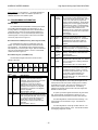
The following steps are required to configure the board for this
function:
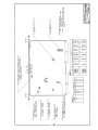
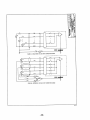
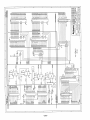
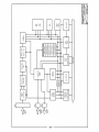
This chapter describes the circuitry of the board. A Block
Diagram of this board is shown in 4500-939.
1. Write 0BH to the Status Register:
Turns off the Red LED (Bit 0 = 1).
•
Turns on the Green LED (Bit 1 = 1).
•
Enables Interrupts (Bit 3 = 1).
•
2. Write the desired interrupt vector to the Vector Register.
3. Write 09H to the Board Control Register:
Selects Continuous Mode (Bit 0 = 1).
•
Allows Acquisition Complete Interrupts to occur (Bit 1 = 0).
•
Selects Software Trigger Type (Bit 2 = 0).
•
Enables Timed Periodic Triggering by enabling the
•
Conversion Timer (Bit 3 = 1).
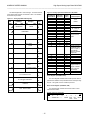
4. Write 80H to the Scan Program Register:
Channel 0 (Bits 0-4 = 0).
•
Gain of 1 (Bits 5-6 = 0).
•
Single channel in the scan sequence (Bit 7 = 1).
•
5. Write 400H (1024) to the Conversion Count Register.
6. Program Conversion Timer for 100 microseconds:
a) Write 54H to the Counter Control Register.
b) Write 02H to the Timer Prescaler.
c) Write 94H to the Counter Control Register.
d) Write 64H (100) to the Conversion Timer.
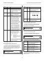
7. Write any byte value to the Start Conversion Register to start the
acquisition.
The Software Trigger initiates the acquisition sequence by
causing an A/D conversion of channel 0. Thereafter the
Conversion Timer will cause A/D conversions of channel 0 every
100 microseconds. After filling each half of the Dual Port RAM,
the state of the Memory Bit (Bit 6 of the Board Status Register)
will change to indicate which half was most recently filled. This
bit could be periodically polled (possibly with a separate task) if
more than 63K samples of pre-trigger A/D data are desired.
32768 (32K) consecutive 16-bit data samples may then be read
from Dual Port RAM starting at the board's base address plus
20000H, if the Memory Bit is a "0" or starting at the board's base
address plus 30000H if the Memory Bit is a "1". The 12-bit A/D
data is left justified in each 16-bit sample.
8. Write any byte value to the Start Conversion Register to stop the
acquisition.
VMEbus INTERFACE
The VMEbus Interface is composed of four functional circuit
areas:
•
•
•
•
Address and data buffers (U41, U42, U55, U58, U59).
Bus control & address decoding (U57, U56, U40, U43,
U34, & U15).
Interrupter (U54, U53, U16).
DC-to-DC Converter (U39).
Bus Control Logic
Comparator U57 decodes the upper 6 address lines (A18-A23)
to see if they correspond to the base address jumper setting (J9).
U57 also makes sure that the VMEbus control lines IACK* and
LWORD* are valid. Programmable Logic Device (PLD) U56
determines if a valid VMEbus data transfer is occuring by monitoring
the output of the comparator, the state of the address modifiers
(AM0-AM5), the address modifier jumper setting (J10) and the
VMEbus data strobes (DS0* and DS1*). U56 also monitors a
control line from the VMEbus Interrupter (IVAL*) to determine if a
valid interrupt acknowledge cycle is occuring. The local control lines
produced by U56 will signal other logic circuits on the board that a
valid data bus transfer is occurring.
U56 also contains the local data bus arbitration circuit for the
Dual Port RAM. This circuit arbitrates the local data bus between a
VMEbus data transfer and the Acquisition Control Logic which
"writes" the A/D data into the Dual Port RAM.
VMEbus Interrupter Logic
PLD U53 inputs control lines which signal when to cause an
interrupt. If interrupts have been enabled and that type of interrupt
has been selected U53 will output an active interrupt pending signal
(IPEND*). The interrupt pending signal causes decoder U54 to drive
one of seven interrupt request lines low (IRQ1*-IRQ7*) depending
on the interrupt level selected by J7. Note that if all three positions of
J7 are open, corresponding to an interrupt level of "0", no interrupt
will be caused even though interrupts may be enabled.
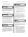
The Software Trigger causes the board to operate in the Block
Mode. The board will now perform 1024 A/D conversions and then
stop, causing an interrupt.
The Interrupt Service Routine may then read 65536 (64K) 16-bit
data samples from Dual Port RAM, starting at the board's base
address plus 20000H, and separate the pre-trigger and post-trigger
data samples.
U53 also monitors the VMEbus interrupt acknowledge input
signal (IACKIN*) and drives the VMEbus interrupt acknowledge
output signal (IACKOUT*). When an active interrupt acknowledge
input occurs U53 first checks to see if the interrupt level of the
interrupt acknowledge (A1-A3) is the same as the interrupt level of
the board as selected by J7. If the interrupt levels match, and U53
has caused an interrupt, then U53 signals the Bus Control Logic that
a valid interrupt acknowledge cycle is occuring. The Vector Register
(U16) contains the interrupt vector which is read during an interrupt
acknowledge cycle. If the interrupt levels do not match, or U53 has
not caused an interrupt, then U53 drives the interrupt acknowledge
output (IACKOUT*) low, passing the interrupt acknowledge on to the
next card.
The last 1024 data samples have been stored sequentially in the
Dual Port RAM starting after the address pointed to by the PreTrigger Data Pointer. This address is found as follows:
a) Read Pre-Trigger-Data-Pointer (PTDP).
b) Multiply PTDP by 2.
c) Add the result from (b) to 20000H.
The address containing last Pre-Trigger Data equals the board's
base address plus 20000H + 2(PTDP).
- 17-